quantum size phenomena in bismuth nanostructures 22sep16.pdf · been dissolved in the h3po4/cro3...
TRANSCRIPT

22/09/2016, Superconducting hybrid nanostructures: physics and application, Dolgoprudni
Quantum size phenomena in
bismuth nanostructures
1Moscow Institute for Electronics and Mathematics at National Research University High
School of Economics, Moscow 2Kapitza Institute for Physical Problems, Russian Academy of Science, Moscow
3NanoScience Centre, University of Jyväskylä, Finland
Konstantin Arutyunov 1,2
K.-P. Riikonen3, E. A. Sedov1

OutlineOutline
Introduction: Quantum Size Effect (QSE)
Existing experiments
Bismuth: properties and fabrication
2D films
1D nanowires
Conclusions
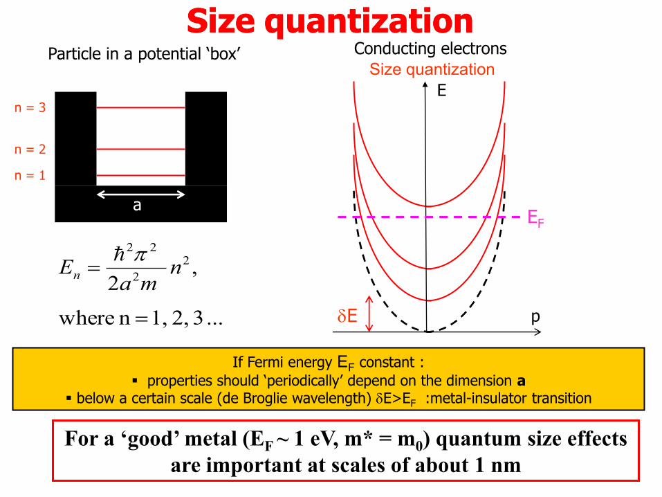
... 3 2, 1, n where
,2
2
2
22
nma
En
a
n = 1
n = 2
n = 3
Particle in a potential ‘box’
Size quantizationSize quantization
dE
EF
E
p
Conducting electrons
If Fermi energy EF constant :
properties should ‘periodically’ depend on the dimension a below a certain scale (de Broglie wavelength) dE>EF :metal-insulator transition
For a ‘good’ metal (EF ~ 1 eV, m* = m0) quantum size effects
are important at scales of about 1 nm
Size quantization

Chewing gum experimentChewing gum experiment G. Rubio, N. Agraït, and S. Vieira,
Atomic-Sized Metallic Contacts: Mechanical Properties and Electronic Transport
Phys. Rev. Lett. 76, 2302 (1996)
Electric conductivity turns to zero
Diameter ~ 0.3 nm
For gold 0.3 nm is about one
interatomic distance…
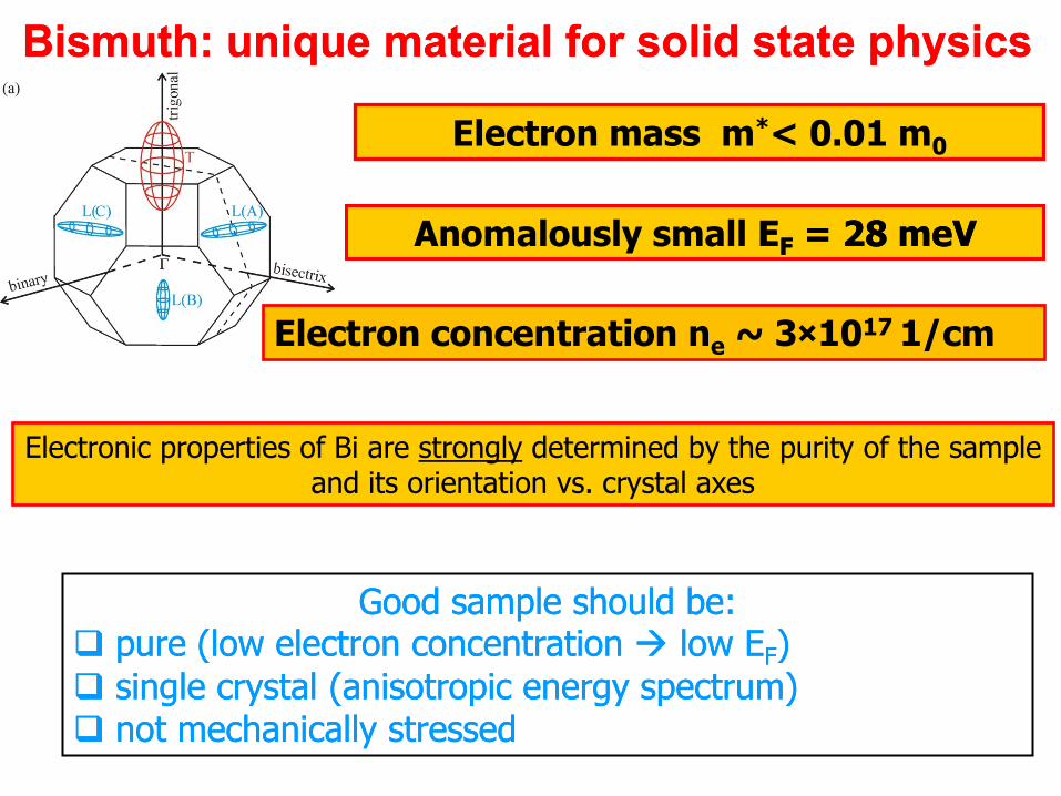
Bismuth: unique material for solid state physicsBismuth: unique material for solid state physics
Electron mass m*< 0.01 m0
Anomalously small EEFF = 28 = 28 meVmeV
Electron concentration ne ~ 3×10¹⁷ 1/cm
Electronic properties of Bi are strongly determined by the purity of the sample and its orientation vs. crystal axes
Good sample should be:Good sample should be: pure (low electron concentration pure (low electron concentration low Elow EFF))
single crystal single crystal (anisotropic energy spectrum)(anisotropic energy spectrum) not mechanically stressednot mechanically stressed
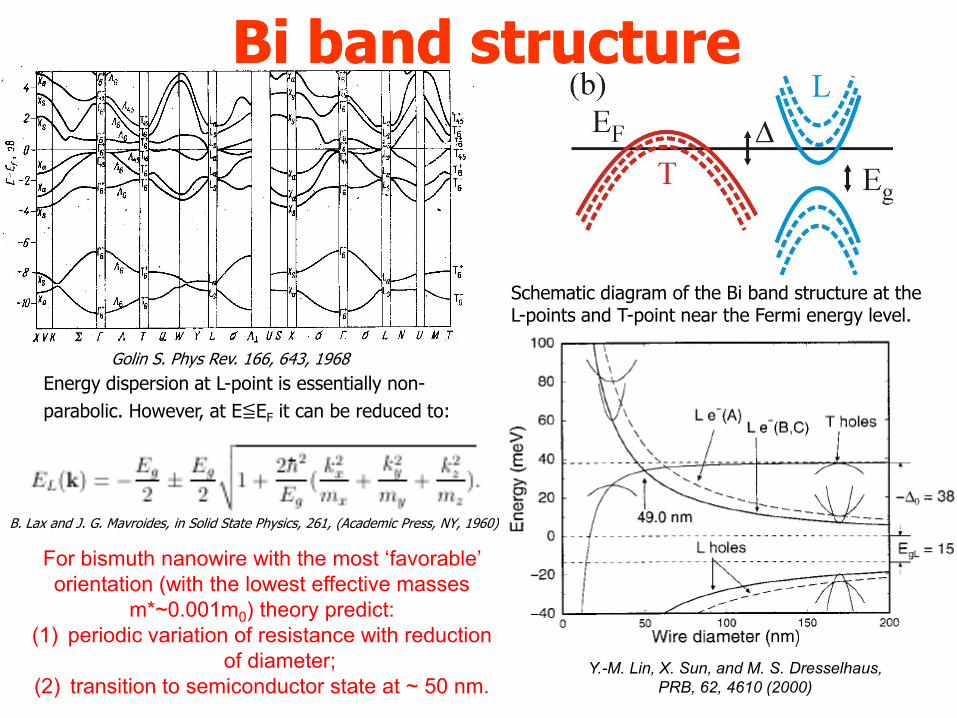
Schematic diagram of the Bi band structure at the L-points and T-point near the Fermi energy level.
Golin S. Phys Rev. 166, 643, 1968
Bi band structureBi band structure
Energy dispersion at L-point is essentially non-
parabolic. However, at E≦EF it can be reduced to:
B. Lax and J. G. Mavroides, in Solid State Physics, 261, (Academic Press, NY, 1960)
For bismuth nanowire with the most ‘favorable’
orientation (with the lowest effective masses
m*~0.001m0) theory predict:
(1) periodic variation of resistance with reduction
of diameter;
(2) transition to semiconductor state at ~ 50 nm. Y.-M. Lin, X. Sun, and M. S. Dresselhaus,
PRB, 62, 4610 (2000)
8
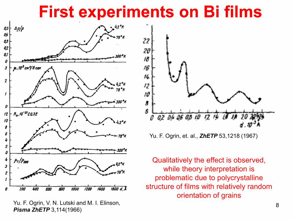
First experiments on Bi filmsFirst experiments on Bi films
Yu. F. Ogrin, et. al., ZhETP 53,1218 (1967)
Yu. F. Ogrin, V. N. Lutski and M. I. Elinson,
Pisma ZhETP 3,114(1966)
Qualitatively the effect is observed,
while theory interpretation is
problematic due to polycrystalline
structure of films with relatively random
orientation of grains

Bi film fabrication: Bi film fabrication:
optimization optimization of of substrate and depositionsubstrate and deposition Substrate Thickness
nm
Pevap,
10-6 mBar
Tevap,
K
Evaporation
rate,
nm/s
rROOM,
10-8W * m
r77K,
10-8W * m
4.2 K
r4.2K,
10-8 W * m
n4.2K,
10+18,1/cm3
m4.2K,
10+4,cm2/Vs
Bulk Bi 150 450 0.3 2
MICA 40 3.1 ~ 300 0.15 221 400 401 10 0.15
150 5.1 ~ 380 0.1 302 842 1106 9 0.07
40 0.68 77 0.15 1588 2192 2300 20±4 0.0068
SiN 40 1.6 ~300 0.16 600±30 1490±70 1510±90 60±20 0.0069
Si 40 1.6 ~300 0.15 572 1320 1476 20 0.02
Bi film on glass deposited @ room T
D.-H. Kim, et. al., Bi on glass, Appl. Surf. Sci, 2005
T= 373 K T= 393 K T= 413 K
T= 433 K T= 448 K T= 473 K
With optimized deposition it is
possible to obtain Bi film on
mica with the grain size of
about 1 mm.

10
2D bismuth film2D bismuth film
2D Bi film on mica
T=4.2 K
Simulated theory curve assumes wide bismuth film
with trigonal axis C3 normal to the sample plane
and random orientation of C2 axes in each grain
C3
C2
C2
C2
150 nm

SEM image of a bundle of Bi nanowires after the alumina template has
been dissolved in the H3PO4/CrO3 solution for 4 days. The Bi chunks on the
right of this image are the remnants of a thin Bi lm left over from the Bi melt
used to inject Bi into the pores[ S.B. Cronin, PhD thesis, MIT 2002].
M.S. Dresselhaus, et.al., PRB 58, R10091 (1998)
M.S. Dresselhaus, et.al., PRB 61, 4850 and 2921 (2000)
not a single wire: array of ’corals’
dirty
not well defined shape
stressed (?)
non-Ohmic I-V (contact or structural problems?)
average diameter > 60 nm
1D limit: Current status of experiments1D limit: Current status of experiments
Long Bi nanowire formed of many grains, no theory fit
is possible [Farhangfar S. PRB 76, 205437 (2007) ]

Single crystalline quasiSingle crystalline quasi--1D bismuth nanostructure1D bismuth nanostructure
After etching
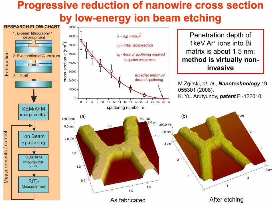
RESEARCH FLOW-CHART
SEM/AFMimage control
Ion Beam
Sputtering
SEM /AFM
Image/profilecontrol
R(T)-Measurement
1. E-beam lithography / development
2. Evaporation of Aluminium
3. Lift-off Fa
bri
ca
tio
nM
ea
su
rem
en
ts /
co
ntr
ol
Progressive reduction of Progressive reduction of nanowirenanowire cross section cross section
by lowby low--energy ion beam etchingenergy ion beam etching
As fabricated
Penetration depth of
1keV Ar+ ions into Bi
matrix is about 1.5 nm:
method is virtually non-
invasive
M.Zgirski, et. al., Nanotechnology 19
055301 (2008).
K. Yu. Arutyunov, patent FI-122010.
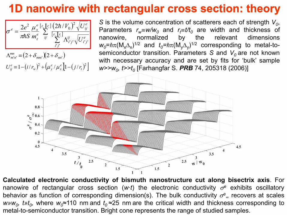
1D 1D nanowirenanowire with rectangular cross section: theorywith rectangular cross section: theory
Calculated electronic conductivity of bismuth nanostructure cut along bisectrix axis. For
nanowire of rectangular cross section (w∙t) the electronic conductivity se exhibits oscillatory
behavior as function of corresponding dimension(s). The bulk conductivity se∞ recovers at scales
w»w0, t»t0, where w0≈110 nm and t0 ≈25 nm are the critical width and thickness corresponding to
metal-to-semiconductor transition. Bright cone represents the range of studied samples.
tw
tw
rr
ijrr
ji
eji
ijji
eij
ez
exe
U
UV
mS
e
''''''
2
02 /22
m
s
S is the volume concentration of scatterers each of strength V0,
Parameters rww/w0 and rtt/t0 are width and thickness of
nanowire, normalized by the relevant dimensions
w0=(MxDx)1/2 and t0=(MyDy)
1/2 corresponding to metal-to-
semiconductor transition. Parameters S and V0 are not known
with necessary accuracy and are set by fits for ‘bulk’ sample
w>>w0, t>>t0 [Farhangfar S. PRB 74, 205318 (2006)] 22/1//1 t
ex
eyw
eij rjriU mm
'''' 22 nnmmmnnm dd
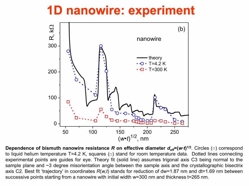
Dependence of bismuth nanowire resistance R on effective diameter deff=(w∙t)1/2. Circles (○) correspond
to liquid helium temperature T=4.2 K, squares (□) stand for room temperature data. Dotted lines connecting
experimental points are guides for eye. Theory fit (solid line) assumes trigonal axis C3 being normal to the
sample plane and ~3 degree misorientation angle between the sample axis and the crystallographic bisectrix
axis C2. Best fit ‘trajectory’ in coordinates R(w,t) stands for reduction of dw=1.87 nm and dt=1.69 nm between
successive points starting from a nanowire with initial width w=300 nm and thickness t=265 nm.
1D 1D nanowirenanowire: experiment: experiment
17
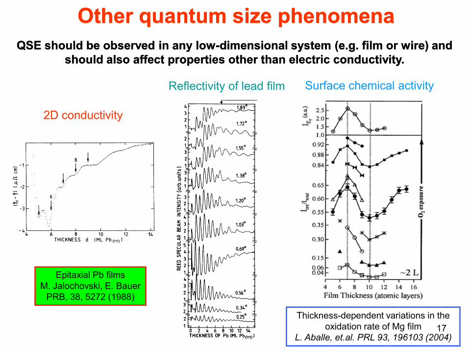
Other quantum size phenomenaOther quantum size phenomena
QSE should be observed in any lowQSE should be observed in any low--dimensional system (e.g. film or wire) and dimensional system (e.g. film or wire) and
should should also affect properties also affect properties other than electric conductivity.other than electric conductivity.
Thickness-dependent variations in the
oxidation rate of Mg film
L. Aballe, et.al. PRL 93, 196103 (2004)
Surface chemical activity Reflectivity of lead film
2D conductivity
Epitaxial Pb films
M. Jalochovski, E. Bauer
PRB, 38, 5272 (1988)

Conclusion on quantum size effect in Conclusion on quantum size effect in
normal metalsnormal metals
• QSE is a universal phenomenon
• Observation of QSE in ‘good’ metals
requires dimensions ~1 nm
• In semimetal like bismuth QSE can
contribute already at 50 nm scales

Master degree
“Quantum Information “Quantum Information
Technology”Technology”
2 year program in English to
start in September 2017