quantitative imaging of the optical near - io.csic.es · tanaka, g. obara, a. zenidaka, m....
TRANSCRIPT
Quantitative imaging of the optical nearfield
Paul Kuhler,1,2,4,5 F. Javier Garcıa de Abajo,3 Philipp Leiprecht,1,2
Andreas Kolloch,1 Javier Solis,2 Paul Leiderer,1 and Jan Siegel2,∗1Faculty of Physics, Universitat Konstanz, Universitatsstraße 10, 78457 Konstanz, Germany
2Instituto de Optica, CSIC, Serrano 121, 28006 Madrid, Spain3Instituto de Quımica Fısica “Rocasolano,” CSIC, Serrano 119, 28006 Madrid, Spain
4Current affiliation: Faculty of Physics, Ludwig-Maximilians-Universitat Munchen,Amalienstraße 54, 80799 Munchen, Germany
[email protected]∗[email protected]
Abstract: When exposing small particles on a substrate to a light planewave, the scattered optical near field is spatially modulated and highlycomplex. We show, for the particular case of dielectric microspheres, that itis possible to image these optical near-field distributions in a quantitativeway. By placing a single microsphere on a thin film of the photosensitivephase change material Ge2Sb5Te5 and exposing it to a single short laserpulse, the spatial intensity modulation of the near field is imprinted intothe film as a pattern of different material phases. The resulting patterns areinvestigated by using optical as well as high-resolution scanning electronmicroscopy. Quantitative information on the local optical near field at eachlocation is obtained by calibrating the material response to pulsed laserirradiation. We discuss the influence of polarization and angle of incidenceof the laser beam as well as particle size on the field distribution. Theexperimental results are in good quantitative agreement with a model basedon a rigorous solution of Maxwell’s equations. Our results have potentialapplication to near-field optical lithography and experimental determinationof near fields in complex nanostructures.
© 2012 Optical Society of America
OCIS codes: (220.4241) Nanostructure fabrication; (240.0240) Optics at surfaces; (290.0290)Scattering.
References and links1. M. Ohtsu, Optical Near Fields: Introduction to Classical and Quantum Theories of Electromagnetic Phenomena
at the Nanoscale (Springer, 2004).2. A. Plech, V. Kotaidis, M. Lorenc, and J. Boneberg, “Femtosecond laser near-field ablation from gold nanoparti-
cles,” Nat. Phys. 2, 44–47 (2005).3. Y. Tanaka, G. Obara, A. Zenidaka, M. Terakawa, and M. Obara, “Femtosecond laser near-field nano-ablation
patterning using Mie resonance high dielectric constant particle with small size parameter,” Appl. Phys. Lett. 96,261103 (2010).
4. E. McLeod and C. B. Arnold, “Subwavelength direct-write nanopatterning using optically trapped microspheres,”Nat. Nanotechnol. 3, 413–417 (2008).
5. H. J. Lezec, “Beaming light from a subwavelength aperture,” Science 297, 820–822 (2002).6. A. Kramer, W. Trabesinger, B. Hecht, and U. P. Wild, “Optical near-field enhancement at a metal tip probed by
a single fluorophore,” Appl. Phys. Lett. 80, 1652–1654 (2002).7. Z. Wang, W. Guo, L. Li, B. Luk’yanchuk, A. Khan, Z. Liu, Z. Chen, and M. Hong, “Optical virtual imaging at
50 nm lateral resolution with a white-light nanoscope,” Nat. Commun. 2, 218 (2011).
#167407 - $15.00 USD Received 7 May 2012; revised 22 Jun 2012; accepted 26 Jun 2012; published 12 Sep 2012(C) 2012 OSA 24 September 2012 / Vol. 20, No. 20 / OPTICS EXPRESS 22063
8. D. Brodoceanu, L. Landstrom, and D. Bauerle, “Laser-induced nanopatterning of silicon with colloidal mono-layers,” Appl. Phys. A. 86, 313–314 (2007).
9. R. Morarescu, L. Englert, B. Kolaric, P. Damman, R. A. L. Vallee, T. Baumert, F. Hubenthal, and F. Trager,“Tuning nanopatterns on fused silica substrates: a theoretical and experimental approach,” J. Mater. Chem. 21,4076–4081, (2011).
10. Z. B. Wang, M. H. Hong, B. S. Luk’yanchuk, Y. Lin, Q. F. Wang, and T. C. Chong, “Angle effect in lasernanopatterning with particle-mask,” J. Appl. Phys. 96, 6845–6850 (2004).
11. A. Pereira, D. Grojo, M. Chaker, P. Delaporte, D. Guay, and M. Sentis, “Laser-fabricated porous alumina mem-branes for the preparation of metal nanodot arrays,” Small 4, 572–576 (2008).
12. P. Leiderer, C. Bartels, J. Konig-Birk, M. Mosbacher, and J. Boneberg, “Imaging optical near-fields of nano-structures,” Appl. Phys. Lett. 85, 5370–5372 (2004).
13. P. Kuhler, F. J. Garcıa de Abajo, J. Solis, M. Mosbacher, P. Leiderer, C. Afonso, and J. Siegel, “Imprinting theoptical near field of microstructures with nanometer resolution,” Small 5, 1825–1829 (2009).
14. J. Siegel, D. Puerto, J. Solis, F. J. Garcıa de Abajo, C. N. Afonso, M. Longo, C. Wiemer, M. Fanciulli, P. Kuhler,M. Mosbacher, and P. Leiderer, “Ultraviolet optical near-fields of microspheres imprinted in phase change films,”Appl. Phys. Lett. 96, 193108 (2010).
15. M. Wuttig, and N. Yamada, “Phase-change materials for rewriteable data storage,” Nat. Mater. 6, 824–832 (2007).16. R. Ovshinsky, “Reversible electrical switching phenomena in disordered structures,” Phys. Rev. Lett. 21, 1450–
1453 (1968).17. V. Weidenhof, I. Friedrich, S. Ziegler, and M. Wuttig, “Laser induced crystallization of amorphous Ge2Sb5Te5
films,” J. Appl. Phys. 89, 3168–3176 (2001).18. Y. Lin, M. H. Hong, T. C. Chong, C. S. Lim, G. X. Chen, L. S. Tan, Z. B. Wang, and L. P. Shi, “Ultrafast-laser-
induced parallel phase-change nanolithography,” Appl. Phys. Lett. 89, 041108 (2006).19. B. Lee, J. Abelson, S. Bishop, D. Kang, B. Cheong, and K. Kim, “Investigation of the optical and electronic
properties of Ge2Sb5Te5 phase change material in its amorphous, cubic, and hexagonal phases,” J. Appl. Phys.97, 1–8 (2005).
20. F. J. Garcıa de Abajo, G. Gomez-Santos, L. A. Blanco, A. G. Borisov, and S. V. Shabanov, “Tunneling mechanismof light transmission through metallic films,” Phys. Rev. Lett. 95, 067403 (2005).
21. G. Mie, “Beitrage zur Optik truber Medien, speziell kolloidaler Metallosungen,” Ann. d. Phys. 330, 377–445(1908).
22. J. M. Liu, “Simple technique for measurements of pulsed gaussian-beam spot sizes,” Opt. Lett. 7, 196–198(1982).
23. B. S. Luk’Yanchuk, Z. B. Wang, W. D. Song, M. H. Hong, “Particle on surface: 3D-effects in dry laser cleaning,”Appl. Phys. A-Mater. 79, 747–751 (2004).
24. J. Siegel, W. Gawelda, D. Puerto, C. Dorronsoro, J. Solis, C. N. Afonso, J. C. G. de Sande, R. Bez, A. Pirovano,and C. Wiemer, “Amorphization dynamics of Ge2Sb5Te5 films upon nano- and femtosecond laser pulse irradia-tion,” J. Appl. Phys. 103, 023516 (2008).
25. H. Ishikawa, H. Tamaru, and K. Miyano, “Microsphere resonators strongly coupled to a plane dielectric substrate:coupling via the optical near field,” J. Opt. Soc. Am. A, Vol. 17, 802-813 (2000).
26. T. Sannomiya, and C. Hafner, “Multiple multipole program modelling for nano plasmonic sensors,” J. Comput.Theor. Nanoscience 7, 1587–1595 (2010).
27. N. Stefanou, V. Yannopapas, and A. Modinos, “Heterostructures of photonic crystals: frequency bands and trans-mission coefficients,” Comput. Phys. Commun. 113, 49-77 (1998).
28. F. J. Garcıa de Abajo, A. Rivacoba, N. Zabala, and P. M. Echenique, “Electron energy loss spectroscopy as aprobe of two-dimensional photonic crystals,” Phys. Rev. B 68, 205105 (2003).
29. F. J. Garcıa de Abajo, “Multiple scattering of radiation in clusters of dielectrics,” Phys. Rev. B 60, 6086–6102(1999).
1. Introduction
The ultimate performance of key technologies in photonics is limited by the diffraction of light,which can be overcome by using optical near fields (ONFs) [1]. ONFs can be generated, forinstance, in the vicinity of metal nanoparticles [2], dielectric spheres [3, 4], subwavelengthapertures [5], or at the tip of an atomic force microscope [6].
In the particular case of dielectric spheres, local intensity distributions can be achieved withsuper-resolution foci, which can be exploited in a white-light optical microscope to achieve50nm lateral resolution [7]. Parallel nanostructuring employing colloidal monolayers of di-electric microspheres has been successfully demonstrated to pattern silicon [8], fused silica [9],as well as GeSbTe [10] and alumina films [11].
#167407 - $15.00 USD Received 7 May 2012; revised 22 Jun 2012; accepted 26 Jun 2012; published 12 Sep 2012(C) 2012 OSA 24 September 2012 / Vol. 20, No. 20 / OPTICS EXPRESS 22064

In order to use ONFs for applications in a predictable and controlled way with maximumprecision, it is essential to have a detailed knowledge of the exact field distribution. A straight-forward method to study local optical field distributions of micro- and nanostructures is toimprint them onto the underlying substrate. This method bears many advantages over classicalnear-field characterization methods such as scanning near-field optical microscopy (SNOM).For example, the system is not disturbed by the scanning microscope tip and the actual imprint-ing of the optical field distribution is done during a very short time (i.e., with a single laserpulse) in contrast to typically time-consuming scanning processes. This minimizes possiblesample degradation effects.
A well-known example of the imprinting technique is the visualization of near fields by localablation of the substrate, in which regions exposed to large field enhancements are ablated,leaving behind a crater whose morphology is related to the shape of the field distribution [12].A major disadvantage of this method is its binary contrast (i.e., ablation/no ablation) and thepresence of non-linear and collateral effects (e.g., debris). Recently, a different method has beendemonstrated [13, 14], which relies on local phase change from crystalline to amorphous in thinchalcogenide films [15]. Laser-induced amorphization requires melting and rapid quenching inorder to prevent nucleation and growth of the crystalline phase. The required high cooling ratesof the molten film can be achieved by using a short (nanosecond) laser pulse and a substratewith high thermal conductivity to act as a heat sink. Here, the imprinted field distribution yieldsa non-binary optical contrast over a large range of illumination intensity and is not affectedby collateral or non-linear effects. Yet, while previous work has reported a general qualitativeagreement in pattern shape between experiment and calculation, a quantitative agreement infield enhancement could not be provided.
In the present work, we demonstrate that it is possible to image ONFs not only in termsof shape but also quantitatively in terms of local field enhancement. The experimental results,imprinting ONFs of dielectric spheres and their variation as a function of particle diameterand light polarization, are in excellent agreement with a model based on solving Maxwell’sequations for a sphere sitting on a layered planar substrate. We also show that high-resolutionSEM studies of imprinted patterns yield well-contrasted ONF images and reveal fine structuresnot resolvable with optical microscopy.
Although in this work we focus on the optical and morphological contrast between the twoGST phases, it is worth mentioning that a phase change is also accompanied by a change inthe electrical resistivity [16], topography [17], and etching resistivity, the latter allowing forparallel production of features with an FWHM below 50nm [18].
This paper is organized as follows. In Section 2, experimental details and a description of themodel and quantitative analysis method are given. In Section 3, the optical response of GST tolaser pulses of different durations (fs, ps, and ns) is examined in detail, which serves the purposeof calibration. The results are then integrated into the calculation to relate the optical response ofONFs to the corresponding field enhancement by comparison with the model. We compare thepatterns produced by spheres of different sizes exposed to laser radiation of different incidentpolarization, illustrating the strong connection between particle size, polarization, and near fielddistribution. In Section 4, we correlate the optical contrast of the patterns used so far to thecontrast obtained from scanning electron microscopy (SEM) measurements [14].
2. Experimental and modeling
2.1. Sample preparation
The samples consisted of 40-nm-thick, face-centered-cubic (fcc) polycrystalline Ge2Sb5Te5
(GST) films sputter-deposited on Si [001] wafers which is covered by a 10-nm-thick amor-phous SiO2 buffer layer, produced by Numonyx, Italy. The optical constants of the different
#167407 - $15.00 USD Received 7 May 2012; revised 22 Jun 2012; accepted 26 Jun 2012; published 12 Sep 2012(C) 2012 OSA 24 September 2012 / Vol. 20, No. 20 / OPTICS EXPRESS 22065

materials at the laser wavelength used in the experiment (800nm) are for fcc-GST: n = 5.72,k = 4.09 [19]; amorphous GST: n = 4.74, k = 1.45 [19]; amorphous SiO2: n = 1.453, k = 0; Si:n = 3.69, k = 0.006. Spherical SiO2 glass particles, dispersed in isopropanol, were depositedunder conditions that ensure particle isolation. The particles used have nominal diameters of660nm, 4.83 μm (Bangs Laboratories, Inc., nominal polydispersity 2% ), and 990nm (DukeScientific Corp., polydispersity < 10%). The size distribution was checked after depositionwith a scanning electron microscope (SEM). It revealed small deviations from the nominalsizes (573± 44nm, 1003± 16nm, and 4645± 27nm, respectively). These values have beenused as input parameters for the calculations presented later on.
Fig. 1. Setup used for irradiation with single laser pulses, including a home-built in-situmicroscope and a movable stage holding the sample. The configuration of the layered sub-strate is also shown.
2.2. Sample irradiation
Laser irradiation of the particle covered films was performed in air using a regeneratively am-plified Ti:sapphire laser system operating at 800nm central wavelength with a pulse duration of120fs, 350ps, or 8ns. The different pulse durations were achieved by compressing the chirpedpulse after amplification (fs), not compressing it (ps), or blocking the fs-laser oscillator seedpulse and operating the amplifier in a Q-switched mode (ns). A sketch of the irradiation schemeis displayed in Fig. 1. The laser beam was focused onto the sample at an angle of incidence of∼ 53◦ to a measured elliptical spot size of 270×150 μm2 (1/e2 diameter). A single pulse wasselected from a 100Hz pulse train by means of an electromechanical shutter to irradiate the tar-geted area. The sample was mounted on a motorized translation stage (three axis) and observedin-situ with a home-built microscope based on a long working distance microscope objective(20x, numerical aperture NA = 0.42) and a tube lens, equipped with a 12bit charge-coupled de-vice (CCD) camera and illuminated by a light emitting diode (LED) (wavelength λ = 400nm).
2.3. Characterization of the imprinted microstructures
Bright-field images of the irradiated regions were recorded ex-situ with a commercial micro-scope (Eclipse, Nikon) using an illumination wavelength of 460nm and a high-magnificationobjective lens (100x, NA = 0.90). Additionally, SEM high-resolution studies were performed
#167407 - $15.00 USD Received 7 May 2012; revised 22 Jun 2012; accepted 26 Jun 2012; published 12 Sep 2012(C) 2012 OSA 24 September 2012 / Vol. 20, No. 20 / OPTICS EXPRESS 22066

with the in-lens detector of a Zeiss Gemini Supra at an accelerating voltage in the range of 5kV,yielding a nominal spatial resolution of 5nm.
2.4. Modeling of the intensity distribution
The spatial electric field distribution at the substrate plane has been calculated by a rigoroussolution of Maxwell’s equations for a sphere sitting on a layered planar substrate, using methodssimilar to those proposed in Ref. [20], and fully elaborated in the appendix. The incident-lightplane wave has a well-defined linear polarization and is incident on the substrate at an angle of53◦. The resulting field is expanded into spherical waves around the sphere, and Mie scatteringtheory [21] is used to determine the resulting outgoing waves. The latter are expressed as planewaves (both propagating and evanescent) moving towards the substrate, and reflected fromthe surface using Fresnel’s coefficients. The reflected plane waves are in turn scattered by thesphere, so that a self-consistent set of equations is written to describe the infinite series ofalternating multiple scattering events at the sphere and the substrate. The system is furtherreduced by integrating over parallel wave vector components of the plane-wave part of thefield, leading to a set of linear equations involving only spherical-wave coefficients, which wesolve for all multipoles up to an orbital angular number l = 24 for full convergence. Finally,the electric field intensity is calculated right underneath the surface, thus giving the fractionof light that penetrates into the film and is absorbed. The latter assumption is justified by theshort penetration length of 16nm for light with a wavelength of 800nm (i.e., no significantinterference is expected as the light propagates within the substrate, so that the dependence ofthe near-field intensity on the distance to the surface is assumed to be a simple exponentialdictated by the skin depth and shared by all points of the surface). Full details of the calculationmethod are given in the appendix.
3. Optical studies
In this chapter, we concentrate on the optical contrast generated upon laser-induced phasechange for analyzing the field distributions imprinted in the GST films. In particular, we showthat a quantitative determination can be achieved. Once the optical response is characterized,this can be applied to the study of different size particles for different polarization of the inci-dent light.
3.1. Optical response of GST to laser irradiation
Figure 2(a) shows an optical micrograph of the surface reflectivity of a GST film after irra-diation with a 350ps pulse. The modified region is elliptically elongated due to the inclinedincidence. The beam has a Gaussian profile, which was characterized by measuring the diam-eter of the amorphous region in the irradiated area at different pulse energies. Therefore, theexact spatial fluence distribution on the substrate surface of the incident beam can be preciselydetermined [22].
In the inset, both the reflectivity and the corresponding fluence distribution are plotted alongthe dashed line in the micrograph. Far away from the spot center, the film is in an unmodified,crystalline state characterized by a reflectivity R0. With increasing fluence, the normalized re-flectivity R/R0 first drops to a minimum value of 0.73, then recovers slightly, and finally endsin a step, which marks the edge of the central ablation crater, where the GST film is completelyremoved from the substrate. From direct comparison of the irradiation fluence with the reflec-tivity of the film after irradiation at a certain position, one can obtain a response function of theGST film for a given set of irradiation parameters (Fig. 2(b)).
For ps pulses, the modification starts at 23mJ/cm2 and the minimum reflecitivity R is reachedat 56mJ/cm2. Between these two values, the reflectivity is a monotonously decreasing function
#167407 - $15.00 USD Received 7 May 2012; revised 22 Jun 2012; accepted 26 Jun 2012; published 12 Sep 2012(C) 2012 OSA 24 September 2012 / Vol. 20, No. 20 / OPTICS EXPRESS 22067

Fig. 2. Optical response of a crystalline GST film to irradiation with single laser pulses ofdifferent durations. (a) Micrograph of the film exposed to irradiation at oblique incidence(τ = 350ps, θ = 53◦ off normal), producing an amorphous ring (regions I and II) aroundthe spot center, where ablation of the GST has taken place (region III). Superimposed is thefluence distribution of the Gaussian beam at the sample surface and the relative reflectivitychange of the film along the dashed line. (b) Relative reflectivity change of the sample as afunction of the local fluence for different pulse durations. The inset shows the reflectivitychange as a function of the thickness of the amorphized top layer of the GST film based ona model assuming interfacial amorphization.
of laser fluence. Keeping the pulse wavelength fixed at 800nm, we have investigated the influ-ence of pulse duration τ on the response of the film. For all three values of τ , the minimumreflectivity is reached at a fluence value three times higher than the onset of amorphization.This implies that in a first approximation the optical response curve can simply be scaled fordifferent τ’s. With increasing τ , the heat flow during the pulse duration of the deposited laserenergy towards the substrate increases, thus efficiently reducing the maximum peak tempera-ture. As a consequence, a higher fluence is required to compensate the heat loss and reach theonset of amorphization for increasing τ , so that the whole response function is stretched over alarger fluence interval [24]. While these results demonstrate that an equivalent optical responsecurve can be obtained for all three (and other intermediate) pulse durations, we concentrate inthe following on results obtained with 350ps pulses.
The behavior of the GST film in the amorphous-response regime can be qualitatively ex-plained by assuming an interfacial transformation of the crystalline GST layer into an amor-phous one, starting from its surface and with the thickness of the transformed layer being amonotonous function of the irradiated fluence [24]. The inset of Fig. 2(b) shows the calcu-lated reflectivity of the system as a function of the thickness of the amorphized GST layer. Themodel gives good qualitative agreement as it well reproduces the recovery below the ablationthreshold.
With these results, any complex pattern with different reflectivity values can be mappeddirectly into the correspondent fluence distribution that created the pattern. Even if this fluencewindow is exceeded, by inverting this analysis a calculated fluence distribution can be convertedinto the expected resulting reflectivity pattern, as shown in the next section.
3.2. Near-field patterns of dielectric spheres: Quantitative analysis
While the relation established above between optical contrast and local fluence is satisfactorybut not too exciting for irradiation of the bare surface with a Gaussian spot, it enables us to
#167407 - $15.00 USD Received 7 May 2012; revised 22 Jun 2012; accepted 26 Jun 2012; published 12 Sep 2012(C) 2012 OSA 24 September 2012 / Vol. 20, No. 20 / OPTICS EXPRESS 22068

analyze and quantify complex spatial field distributions, which form upon irradiation of scatte-ring particles. The micrograph depicted in Fig. 3(a) shows the result of such an irradiation fora 350ps pulse on a SiO2 particle with a diameter of 1.00 μm, which was removed upon irradia-tion. Its position can be determined from the ablation hole that is left behind at the focal positionof the particle and is indicated by a white dot. Due to the oblique incidence (θ = 53◦, from theleft), the imprinted pattern, composed of amorphous and crystalline regions, is elliptically elon-gated and only symmetrical with respect to the horizontal axis through the particle center. Inthe intermediate vicinity of the particle, the pattern is complex, in contrast to the far field of thescattering particle where the period p of the observed fringes along the surface-projected for-ward and backward light propagation directions equals a constant value (pf w,exp = 3.9 μm andpbw,exp = 440nm, respectively). A simple calculation of the interference of a spherical wave forthe scattered light with the incident plane wave yields pf w = λinc/(1− sinθ) = 3.97 μm alongthe forward direction and pbw = λinc/(1+ sinθ) = 445nm along the backward direction, bothin good agreement with the measured value.
Fig. 3. Quantitative comparison between the optical near-field imprint produced by irra-diation of a single dielectric sphere on the GST film and the corresponding calculation.(a) Optical micrograph of the GST film after irradiation with a 350ps pulse (θ = 53◦)on a sphere (diameter d = 1.00 μm), which was removed upon irradiation. The particle’soriginal position is marked with a white dot. Also shown is the corresponding calculatedintensity distribution as well as the intensity profile along the white dashed line (both asinsets). (b) Reflectivity profiles along the horizontal axis through the center of the sphere.The experimental data were taken along the black dashed line in (a). Calculated data areobtained from mapping the theoretical intensity profile shown in the inset of (a) into reflec-tivity values (see main text for details).
For a deeper understanding of the field distribution in the particle near field, it is necessaryto compare the resulting pattern with a calculation that takes into account the whole system andtherefore also includes the influence of the substrate. The need for such a comparison becomesobvious if one looks at the close vicinity of the particle, where the far-field condition is not met.The shadowing effect of the particle cannot explain the considerable spatial extension of theapparently unmodified, bright region around the ablation hole that is much larger than the par-ticle projection onto the surface. Using the model described in section 2, the two-dimensionalintensity distribution I/I0 (x,y) for the present arrangement was calculated and is depicted as aninset in Fig. 3(a). For a qualitative, spatial comparison with experiment, these values are shownwith an inverted color scale (i.e. dark regions mark field enhancement whereas brighter regionsmark field attenuation). In this way the calculations reflect the GST behavior as an approximateopposite linear function of the local fluence upon irradiation.
#167407 - $15.00 USD Received 7 May 2012; revised 22 Jun 2012; accepted 26 Jun 2012; published 12 Sep 2012(C) 2012 OSA 24 September 2012 / Vol. 20, No. 20 / OPTICS EXPRESS 22069

Since I/I0 (x,y) ∝ F/F0 (x,y), the value of I0 can be directly determined from the measuredpulse peak fluence Fmax = 18.6mJ/cm2 at the beam center position. Finally, the profile wasconvoluted with a Gaussian function which simulates the limitation in spatial resolution im-posed by the imaging system. The result, displayed in Fig. 3(b), shows an excellent agreementbetween calculation and experiment. Deviations are in the range of only a few percent, exceptfor the range 0 < x < 1 μm, where the particle focuses the incoming light down to a very smallarea, leading to strong local ablation in this region.
3.3. Influence of the particle size on the imprinted pattern
To investigate the influence of particle size on the field distribution, we irradiated colloidalspheres of different diameters (Fig. 4). The laser beam was polarized perpendicular to the inci-dent plane (s-polarized). In all cases, the particles have been removed upon irradiation.
Fig. 4. Near-field imprints from particles of different sizes. (a) Optical micrograph of theGST film after irradiation with a 350 ps pulse (θ = 53◦) on a single sphere (d = 4.65 μm).The calculated intensity distribution is shown as an inset. (b) Same as (a) for d = 1.00 μm.(c) Same as (a) for d = 0.57 μm. (d) Lower part: Calculated intensity distribution from(a). Upper part: Calculated intensity distribution for a particle diameter that is only 25nmsmaller than in (a).
With increasing particle size, two trends become apparent: Firstly, the near-field pattern ismore complex for larger particles. The smallest particles investigated, with a diameter compa-rable to the wavelength of the incident light, display a characteristic pattern similar to that ofa simple dipole (Fig. 4(c)). In contrast, the situation is more complex for bigger particles (Fig.4(a)). This applies only to the near-field of the particles (i.e. up to distances that are compa-rable to the diameter of the scattering particle). For all investigated particle sizes, at distancesx ≥ 2d from the particle center, the diameter-independent far-field behavior of the modulationperiods quoted above (p f w/bw = λinc/(1± sinθ)) holds quite satisfactorily. The second effect,which also concerns the far-field of the particles, is that the amplitude of the interference patterndecreases with the particle size, in agreement with the smaller scattering cross section.
#167407 - $15.00 USD Received 7 May 2012; revised 22 Jun 2012; accepted 26 Jun 2012; published 12 Sep 2012(C) 2012 OSA 24 September 2012 / Vol. 20, No. 20 / OPTICS EXPRESS 22070

As in the previous figure, the agreement between imprints and calculated intensity distribu-tions is very good. However, for the largest particle there are some differences in the ”shadowregion” to the left of the ablation hole (c.f. arrow in Fig. 4(a)). In particular, the calculation pre-dicts a field enhancement fine structure in contrast to the experimental pattern, where the film isfound to remain in its original crystalline phase at this position. In order to estimate the effect ofsmall deviations in the particle size used for the calculation, the field distribution for a particlewith a diameter only 25nm smaller (i.e. within the margin of error of the measurement) wascalculated and compared to the one shown in Fig. 4(a). Both results cannot be distinguishedwhen examining only the forward-scattering part, but they feature significant differences in theshadow region. The subtle modulation in the field distribution at this position vanishes com-pletely for the smallest particle (black arrow), which fits well to the experimentally resultingpattern. Those subtle field enhancements in the shadow region of the particle are in agreementwith calculation results of previous work by Luk’Yanchuk et al. [23].
Fig. 5. Near-field imprints of particles with diameter d = 1.00 μm for different linear po-larizations of the 350ps laser pulse. (a) Micrograph of a pattern produced with p-polarizedlight. The calculated intensity distribution is shown as an inset. (b) Same as (a) for s-polarized light. (c) Reflectivity profile along a line in the incident plane and through theparticle center (at x = 0) in (a) and (b). (d) Corresponding calculated intensity profiles.
The polarization of the incident light also has a great influence on the imprinted pattern.Figure 5 shows two patterns that are the result of irradiations on particles of the same size (d =1.00 μm) but for different beam polarizations. Besides the obvious differences in the shape ofboth imprints, more subtle features can be distinguished when plotting the horizontal reflectivityprofiles through the particle center for both polarizations (Fig. 5(c)). The forward-scattering partof the pattern produced by p-polarized light is much more pronounced than for s-polarized light.The opposite behavior is observed for the back-scattering and side parts, which accordinglyare visible over a much larger area in Fig. 5(b). Both observations are in agreement with thecorresponding calculation, which predicts this exact relative local field amplification (Fig. 5(d)).
4. SEM studies
The optical studies reported in section 3 demonstrate the ability of our method to image opticalnear-fields in a quantitative manner. Yet, a higher spatial resolution, as provided by SEM, isdesirable as it can resolve even the smallest features within the imprinted patterns. In order
#167407 - $15.00 USD Received 7 May 2012; revised 22 Jun 2012; accepted 26 Jun 2012; published 12 Sep 2012(C) 2012 OSA 24 September 2012 / Vol. 20, No. 20 / OPTICS EXPRESS 22071

to use SEM for this purpose, the SEM contrast produced by laser-induced modification of acrystalline GST film needs to be characterized as a first step.
4.1. Characterization of SEM contrast in laser irradiated GST film
Figure 6 shows a comparison of a SEM micrograph with an optical-microscope image, bothtaken at the same spot. The pulse energy was much higher than that used in Fig. 2. Thus, theablation crater is larger and includes a second ring, which marks the onset of ablation of theSiO2 buffer layer underneath. Interestingly, at this magnification it is difficult to distinguishthe amorphous region from the surrounding crystalline film with SEM. Only the regions atirradiation fluences well within the amorphization regime show up in SEM, slightly darker thanthe neighboring surface to the right. In order to understand the origin of the different SEMcontrast in the amorphous part of the spot, a series of regions along the horizontal axis throughthe beam center position were investigated at higher resolution. Due to carbon deposition duringthe SEM scans, these regions appear darker in the overview shown in Fig. 6.
At the position that is furthest away from the irradiated area (position 7(a) in Fig. 6), the highresolution SEM scan reveals the characteristic roughness of the unmodified, polycrystallineGST film (Fig. 7(a)). In the intermediate amorphous region, which shows little difference withrespect to the crystalline surface observed with SEM at low magnification, ripples of largerperiod show up at high magnification (Fig. 7(b)). Finally, at the position nearest to the ablationthreshold (full amorphization), the surface becomes smooth (Fig. 7(b)).
Fig. 6. Upper part: Optical micrograph of a zoomed region of an irradiated area withoutparticles (τ = 350ps). From right to left, the intensity increases and gives rise to differentoptical response of the sample: (i) crystalline GST film, (ii) partially amorphized GST film,(iii) completely amorphized GST film (iv) ablation of GST film, and (v) ablation of bufferlayer. Lower part: SEM micrograph of the same irradiated spot. The darkened rectangularregions were investigated at higher resolution (see Fig. 7).
In order to analyze the surface morphology in more detail, the images were processed withfast Fourier transform (FFT). An example of the result of FFT is displayed for Fig. 7(b) as aninset. Subsequently, the isotropic distributions were radially averaged for noise reduction. Theresulting contour plots were then normalized to their mean values at high frequencies, wherethe signal distribution is nearly homogeneous. The signal artifacts introduced by FFT due tolimited dimensions of the processed images were eliminated in the data obtained from Fig. 7(a)and (b) by subtracting the result of Fig. 7(c), since no characteristic frequency band was found.
#167407 - $15.00 USD Received 7 May 2012; revised 22 Jun 2012; accepted 26 Jun 2012; published 12 Sep 2012(C) 2012 OSA 24 September 2012 / Vol. 20, No. 20 / OPTICS EXPRESS 22072

Fig. 7. (a)-(c) SEM micrographs of the GST film in different states (marked in Fig. 6).(a) crystalline GST, (b) partially amorphized GST, and (c) completely amorphized GST.The Fourier transforms of all images (example shown for (b)), radially integrated and nor-malized, are plotted in the graphs below. The result from (c) mainly consists of backgroundnoise (see graph inset: signal vs. periodicity), which is common to all transforms and whichwas therefore subtracted from the results of (a) and (b), displaying signal difference versusperiodicity in the plot.
The final result reveals that the ripples in the partly amorphous region do not replace, but rathersuperimpose, the roughness that is inherited by the crystalline film. Namely, the only differencebetween (a) and (b) is the formation of a sharp peak at a period of ∼ 130nm, which adds to theless pronounced peak at a period of ∼ 40nm. This is the grain size of the as-grown crystallineGST film. Both structural components vanish at larger fluence (c), leaving behind a smooth,fully amorphous GST film.
In summary, we find that depending on the local fluence the GST film yields a ternary SEMcontrast: Crystalline with a grain size of 40nm (I), partially amorphized with superimposedripples of a period three times larger than the crystalline film grain size (II), and completelyamorphous and smooth (III). Identification of this behavior enables us to carry out an advancedinterpretation of complex near field patterns imprinted when irradiating the GST film with aparticle on top of it.
4.2. SEM investigation of near field patterns
High-resolution images are especially interesting in the region of the pattern back-scattering,where the period of the produced structure is very small and cannot be resolved completely withoptical microscopy. An illustrative SEM micrograph of a pattern produced by a particle withd = 4645nm is shown in Fig. 8(a) along with the corresponding calculation. The pattern con-tains features corresponding to all three regimes identified above. Most fringes are composedof ripples (regime II), the space between fringes and the shadow region is unmodified (regimeI) and the first fringe, close to the shadow region, is smooth and dark (regime III). The ripple
#167407 - $15.00 USD Received 7 May 2012; revised 22 Jun 2012; accepted 26 Jun 2012; published 12 Sep 2012(C) 2012 OSA 24 September 2012 / Vol. 20, No. 20 / OPTICS EXPRESS 22073

period coincides with the one observed in the type-II contrast regime, as discussed before.The level of detail that can be accessed using SEM becomes clear when examining
the ”shadow region” of the irradiated particle. The region around the ablation hole is notcompletely unmodified, as one could erroneously deduce from the optical-microscope results.Instead, the fine tips of the imprinted interference maxima almost reach the ablation hole(white arrow). These subtle structures are also predicted by the calculation.
Fig. 8. SEM-micrographs of the near-field pattern of a particle (diameter d = 4645nm)at the position where it was located before irradiation (τ = 350ps). The correspondingcalculated intensity distribution is shown as an inset in (a). (b) Upper part: taken from theSEM micrograph shown in (a). Lower part: taken from a SEM micrograph of a pattern of aparticle with the same size but exposed to lower pulse energy.
In Fig. 8(b), the SEM image of (a) is contrasted with another irradiation at lower pulse energy(lower half of the picture). The lower amount of deposited energy leads to less pronounced fea-tures in the imprint. Regarding the inner-most fringes located in the vicinity of the ”shadow”,not only the width but also the contrast type is different. In the upper part of the figure, thesefringes are mainly of type-III contrast (smooth and dark borders), whereas in the lower part, atthe corresponding location, only a type-II contrast (with ripples) is found. A comparison withtheory in Fig. 8(a) confirms that the type III-contrast regions are formed at positions of highintensity. This leads to the conclusion that the fluence-dependent surface morphology that isobserved upon laser irradiation of the bare GST film is also maintained at a much smaller scale.Accordingly, the altered regions in the particle pattern correspond to the calculated field en-hancements not only in terms of shape, but also quantitatively in a sense of the ternary contrastof the bare GST surface as discussed above. Finally, it appears that the smallest feature size thatis possible to be produced with this technique is not yet reached as the surface roughness is stillsmaller than the imprinted pattern period.
5. Conclusions
We have demonstrated that the imprinting of optical near-fields originating from single col-loidal particles in GST films enables the imaging of complex field distributions in full detailand even quantitative analysis of the so-produced features. The particle size and the polariza-tion of the incoming light are found to have a strong influence on the form and modulation depthof the imprints. The results are quantitatively matched with calculations based on rigorous so-lution of the Maxwell’s equations with only small deviations within a few percent. Opticalcontrast allows for the visualization of a high dynamic range of field distributions, whereas
#167407 - $15.00 USD Received 7 May 2012; revised 22 Jun 2012; accepted 26 Jun 2012; published 12 Sep 2012(C) 2012 OSA 24 September 2012 / Vol. 20, No. 20 / OPTICS EXPRESS 22074
SEM imaging shows that the GST film yields a ternary contrast in the crystalline-amorphousregime. High-resolution SEM images show the capability of GST films to record the fine struc-ture of optical near-fields in great detail, in excellent agreement with theoretical calculations.Further down-scaling of optically written patterns in GST films seems to be possible and weare currently identifying suitable structures to produce such small scattering field distributions.Our technique is inherently applicable to other types of scattering particles, such as plasmoniccolloids.
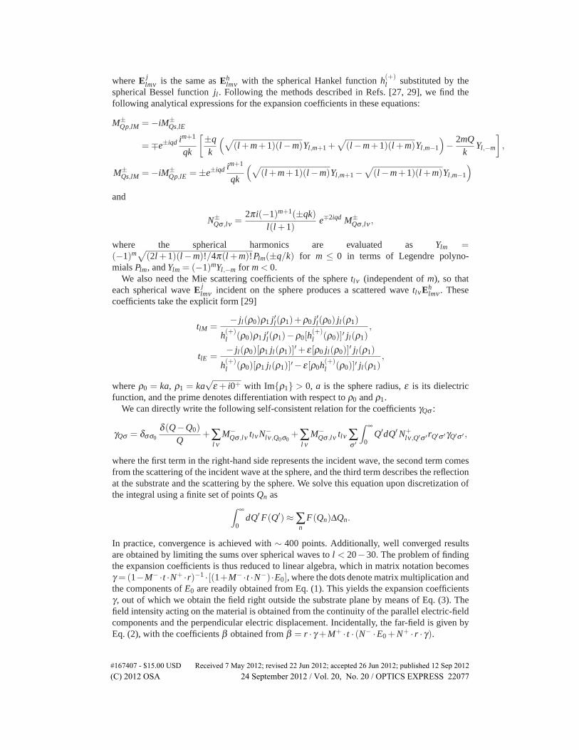
6. Appendix
In this appendix we provide a semi-analytical method to solve Maxwell’s equations for thegeometry of the samples examined in this paper. Alternative methods to describe equivalentsituations have been reported previously [23, 25]. We consider a spherical particle placed closeto a substrate, as shown in Fig. 9, illuminated by a light plane wave coming from region I.We solve the electromagnetic field in this configuration by expanding it in terms of planeand spherical waves in the three regions shown in the Fig. and then matching them at theirboundaries. Similar methods have been used for other configurations, and they are generallyknown as multiple multipolar expansions [26]. We work in frequency space, so that the nota-tion E(r, t) = E(r)exp(−iωt)+ c.c. is used for the fields. The origin r = 0 is chosen at thesubstrate point that is closest to the sphere.
In the numerical calculations shown in this paper, we introduce Fresnel’s coefficients to rep-resent the layered substrate used in the experiment. The resulting reflection coefficients can beexpressed in terms of the Fresnel coefficients of each interface, as explained in Ref. [27].
a
Region I
z=0R
z
b
Region II
Region III
Substrate
Fig. 9. Elements used in the description of the response of a homogeneous spherical particleof radius a sitting near a substrate. We eventually set b = a in the calculations reported inthis paper.
The incident plane wave has wave vector components Q0 along the x and y directions parallel
to the substrate and −q0 = −√
k2 −Q20 + i0+ along z, where k is the light wave vector in the
air medium above the substrate and the sign of the square root is chosen to yield Im{q0} > 0.Given the symmetry of the sphere-substrate system, it is convenient to expand the incidentelectric field, taken to have unit amplitude, in terms of cylindrical waves as
E0(r) =
⎧⎪⎨⎪⎩
epeiQ0·R−iq0z =−∑m imE−Q0mp, for σ0 = p polarization,
eseiQ0·R−iq0z = ∑m im+1E−Q0ms, for σ0 = s polarization,
(1)
#167407 - $15.00 USD Received 7 May 2012; revised 22 Jun 2012; accepted 26 Jun 2012; published 12 Sep 2012(C) 2012 OSA 24 September 2012 / Vol. 20, No. 20 / OPTICS EXPRESS 22075

where ep and es are the polar and azimuthal unit vectors, respectively, and
E±Qms =
[imQR
Jm(QR)R− J′m(QR)ϕ]
eimϕe±iqz,
E±Qmp =±q
k
[iJ′m(QR)R− m
QRJm(QR)ϕ ± Q
qJm(QR)z
]eimϕe±iqz
form a complete basis set of cylindrical waves (see the appendix of Ref. [28] for further detailson these types of waves). Here, R and ϕ are the polar coordinates of R = (x,y), the origin of z isat the substrate plane, and q =
√k2 −Q2 + i0+. We can solve the problem separately for each
azimuthal component m and then sum the results with the same coefficients as in the expansionof Eq. (1).
We thus need to find the self-consistent electromagnetic field for each incident cylindricalwave E−
Q0mσ0of parallel wave vector Q0, polarization σ0, and azimuthal number m. The electric
field in region I becomes
E = E−Q0mσ0
+∑σ
∫ ∞
0QdQβQσ E+
Qmσ , (2)
where rQσ is the Fresnel reflection coefficient of the layered substrate for polarization σ andparallel wave vector Q, and the second term on the right hand side comes from the scatteringproduced by the sphere and the substrate, expressed in terms of cylindrical waves with expan-sion coefficients βQσ . Likewise, the field in region III can be written
E = ∑σ
∫ ∞
0QdQγQσ
[E−
Qmσ + rQσ E+Qmσ
]. (3)
Finally, the field in region II contains the waves impinging into it (i.e., the incident wave andthe waves reflected at the substrate) plus the spherical waves scattered out of the sphere:
E = E−Q0mσ0
+∑σ
∫ ∞
0QdQγQσ rQσ E+
Qmσ +∑lσ
αlσ Ehlmν ,
where
EhlmM = Lh(+)
lm (r− r0),
EhlmE = (−i/k)∇×Lh(+)
lm (r− r0)
are spherical outgoing waves of magnetic (M) and electric (E) polarization, L =−i(r−r0)×∇is the orbital angular momentum operator relative to the center of the sphere r0, and h(+)
lm (r) =
ilh(+)l (kr)Ylm(r) is an outgoing scalar spherical wave (see Ref. [29] for more details on spherical
waves).Obviously, we need to transform the electric field back and forth between spherical and
cylindrical waves. The spherical outgoing waves produced by scattering at the sphere can bewritten in terms of cylindrical waves as
Ehlmν = ∑
σ
∫ ∞
0QdQM±
Qσ ,lνE±Qmσ ,
where the + (−) sign stands for waves propagation above (below) the sphere, away from it.Likewise, the cylindrical waves incident on the sphere can be expanded in spherical waves as
E±Qmσ =
∞
∑l=|m|
∑ν
N±lν ,Qσ E j
lmν ,
#167407 - $15.00 USD Received 7 May 2012; revised 22 Jun 2012; accepted 26 Jun 2012; published 12 Sep 2012(C) 2012 OSA 24 September 2012 / Vol. 20, No. 20 / OPTICS EXPRESS 22076
where E jlmν is the same as Eh
lmν with the spherical Hankel function h(+)l substituted by the
spherical Bessel function jl . Following the methods described in Refs. [27, 29], we find thefollowing analytical expressions for the expansion coefficients in these equations:
M±Qp,lM =−iM±
Qs,lE
=∓e±iqd im+1
qk
[±qk
(√(l +m+1)(l−m)Yl,m+1 +
√(l −m+1)(l+m)Yl,m−1
)− 2mQ
kYl,−m
],
M±Qs,lM =−iM±
Qp,lE =±e±iqd im+1
qk
(√(l +m+1)(l−m)Yl,m+1 −
√(l −m+1)(l+m)Yl,m−1
)
and
N±Qσ ,lν =
2πi(−1)m+1(±qk)l(l +1)
e∓2iqd M±Qσ ,lν ,
where the spherical harmonics are evaluated as Ylm =(−1)m
√(2l +1)(l −m)!/4π(l +m)!Plm(±q/k) for m ≤ 0 in terms of Legendre polyno-
mials Plm, and Ylm = (−1)mYl,−m for m < 0.We also need the Mie scattering coefficients of the sphere tlν (independent of m), so that
each spherical wave E jlmν incident on the sphere produces a scattered wave tlνEh
lmν . Thesecoefficients take the explicit form [29]
tlM =− jl(ρ0)ρ1 j′l(ρ1)+ρ0 j′l(ρ0) jl(ρ1)
h(+)l (ρ0)ρ1 j′l(ρ1)−ρ0[h
(+)l (ρ0)]′ jl(ρ1)
,
tlE =− jl(ρ0)[ρ1 jl(ρ1)]
′+ ε[ρ0 jl(ρ0)]′ jl(ρ1)
h(+)l (ρ0)[ρ1 jl(ρ1)]′ − ε[ρ0h(+)
l (ρ0)]′ jl(ρ1),
where ρ0 = ka, ρ1 = ka√
ε + i0+ with Im{ρ1} > 0, a is the sphere radius, ε is its dielectricfunction, and the prime denotes differentiation with respect to ρ0 and ρ1.
We can directly write the following self-consistent relation for the coefficients γQσ :
γQσ = δσσ0
δ (Q−Q0)
Q+∑
l νM−
Qσ ,lν tlν N−lν ,Q0σ0
+∑l ν
M−Qσ ,lν tlν ∑
σ ′
∫ ∞
0Q′dQ′ N+
lν ,Q′σ ′rQ′σ ′γQ′σ ′ ,
where the first term in the right-hand side represents the incident wave, the second term comesfrom the scattering of the incident wave at the sphere, and the third term describes the reflectionat the substrate and the scattering by the sphere. We solve this equation upon discretization ofthe integral using a finite set of points Qn as
∫ ∞
0dQ′ F(Q′)≈ ∑
nF(Qn)ΔQn.
In practice, convergence is achieved with ∼ 400 points. Additionally, well converged resultsare obtained by limiting the sums over spherical waves to l < 20−30. The problem of findingthe expansion coefficients is thus reduced to linear algebra, which in matrix notation becomesγ =(1−M− ·t ·N+ ·r)−1 · [(1+M− ·t ·N−) ·E0], where the dots denote matrix multiplication andthe components of E0 are readily obtained from Eq. (1). This yields the expansion coefficientsγ , out of which we obtain the field right outside the substrate plane by means of Eq. (3). Thefield intensity acting on the material is obtained from the continuity of the parallel electric-fieldcomponents and the perpendicular electric displacement. Incidentally, the far-field is given byEq. (2), with the coefficients β obtained from β = r · γ +M+ · t · (N− ·E0 +N+ · r · γ).
#167407 - $15.00 USD Received 7 May 2012; revised 22 Jun 2012; accepted 26 Jun 2012; published 12 Sep 2012(C) 2012 OSA 24 September 2012 / Vol. 20, No. 20 / OPTICS EXPRESS 22077

Acknowledgments
We would like to thank Alejandro Ruiz de la Cruz for his clever idea on how to switch quicklybetween laser pulses of different durations in the irradiation setup. This work was performedwithin a Joint Project between CSIC and Konstanz University funded by the Spanish Govern-ment and the DAAD. We also acknowledge partial funding from Spanish National ResearchProjects (Grants No. TEC2011-22422 and TEC2008-01183, MAT2010-14885, and ConsoliderNanoLight.es) and by Deutsche Forschungsgemeinschaft (SFB 767 and SPP1327).
#167407 - $15.00 USD Received 7 May 2012; revised 22 Jun 2012; accepted 26 Jun 2012; published 12 Sep 2012(C) 2012 OSA 24 September 2012 / Vol. 20, No. 20 / OPTICS EXPRESS 22078