quantax eds - high-performance scientific instruments …€¦ · · 2017-09-01quantax eds...
TRANSCRIPT
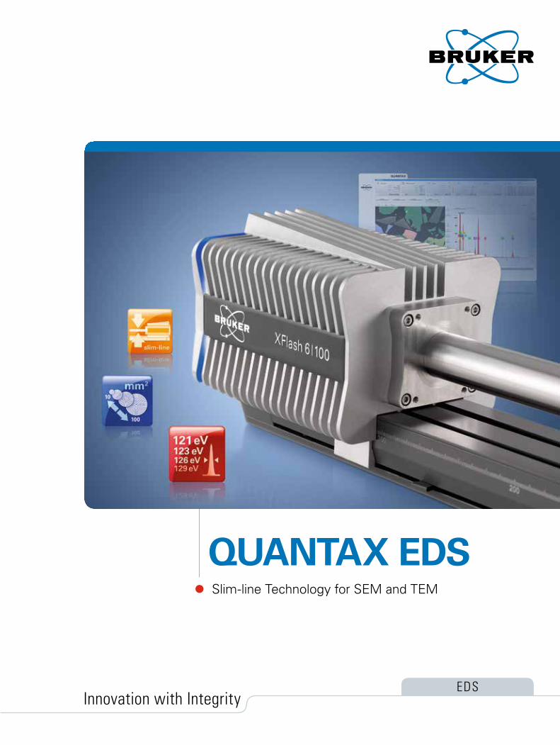
QUANTAX EDS Slim-line Technology for SEM and TEM
EDSInnovation with Integrity
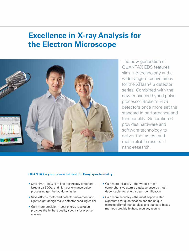
Excellence in X-ray Analysis for the Electron Microscope
The new generation of QUANTAX EDS features slim-line technology and a wide range of active areas for the XFlash® 6 detector series. Combined with the new enhanced hybrid pulse processor Bruker’s EDS detectors once more set the standard in performance and functionality. Generation 6 provides hardware and software technology to deliver the fastest and most reliable results in nano-research.
� Save time – new slim-line technology detectors, large area SDDs, and high performance pulse processing get the job done faster
� Save effort – motorized detector movement and light weight design make detector handling easier
� Gain more precision – best energy resolution provides the highest quality spectra for precise analysis
� Gain more reliability – the world’s most comprehensive atomic database ensures most dependable low energy peak identification
� Gain more accuracy – the most sophisticated algorithms for quantification and the unique combinability of standardless and standard-based methods provide highest accuracy results
QUANTAX – your powerful tool for X-ray spectrometry
Excellence in X-ray Analysis for the Electron Microscope
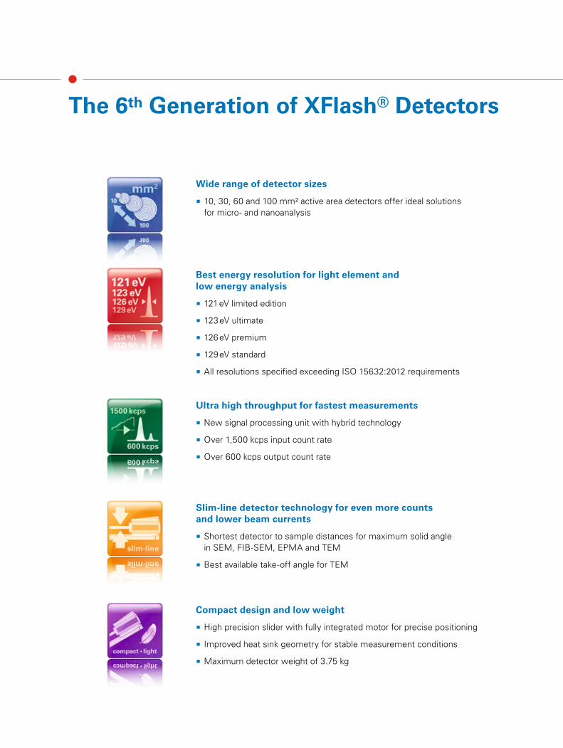
The 6th Generation of XFlash® Detectors
Wide range of detector sizes
� 10, 30, 60 and 100 mm² active area detectors offer ideal solutions for micro- and nanoanalysis
Best energy resolution for light element and low energy analysis
� 121 eV limited edition
� 123 eV ultimate
� 126 eV premium
� 129 eV standard
� All resolutions specified exceeding ISO 15632:2012 requirements
Ultra high throughput for fastest measurements
� New signal processing unit with hybrid technology
� Over 1,500 kcps input count rate
� Over 600 kcps output count rate
Slim-line detector technology for even more counts and lower beam currents
� Shortest detector to sample distances for maximum solid angle in SEM, FIB-SEM, EPMA and TEM
� Best available take-off angle for TEM
Compact design and low weight
� High precision slider with fully integrated motor for precise positioning
� Improved heat sink geometry for stable measurement conditions
� Maximum detector weight of 3.75 kg
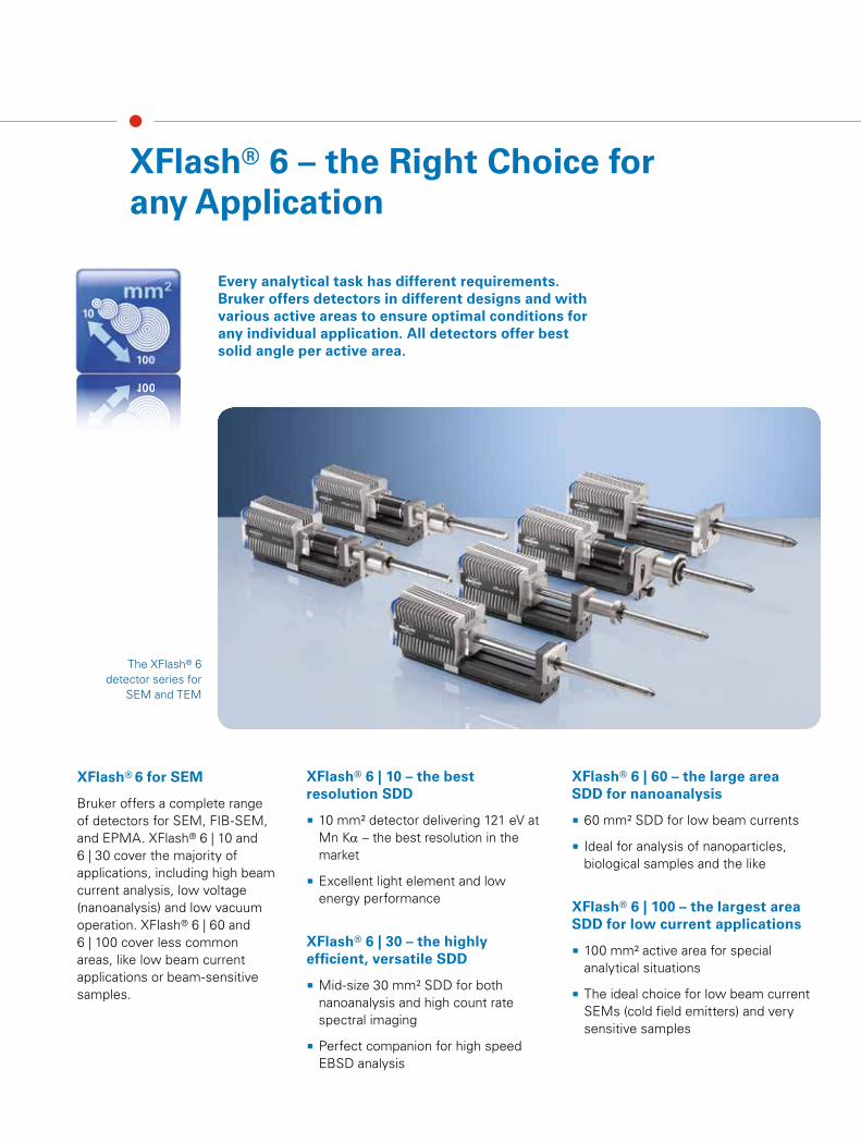
XFlash® 6 for SEM
Bruker offers a complete range of detectors for SEM, FIB-SEM, and EPMA. XFlash® 6 | 10 and 6 | 30 cover the majority of applications, including high beam current analysis, low voltage (nanoanalysis) and low vacuum operation. XFlash® 6 | 60 and 6 | 100 cover less common areas, like low beam current applications or beam-sensitive samples.
Every analytical task has different requirements. Bruker offers detectors in different designs and with various active areas to ensure optimal conditions for any individual application. All detectors offer best solid angle per active area.
XFlash® 6 – the Right Choice for any Application
The XFlash® 6 detector series for
SEM and TEM
XFlash® 6 | 10 – the best resolution SDD
� 10 mm² detector delivering 121 eV at Mn Ka – the best resolution in the market
� Excellent light element and low energy performance
XFlash® 6 | 30 – the highly efficient, versatile SDD
� Mid-size 30 mm² SDD for both nanoanalysis and high count rate spectral imaging
� Perfect companion for high speed EBSD analysis
XFlash® 6 | 60 – the large area SDD for nanoanalysis
� 60 mm² SDD for low beam currents
� Ideal for analysis of nanoparticles, biological samples and the like
XFlash® 6 | 100 – the largest area SDD for low current applications
� 100 mm² active area for special analytical situations
� The ideal choice for low beam current SEMs (cold field emitters) and very sensitive samples
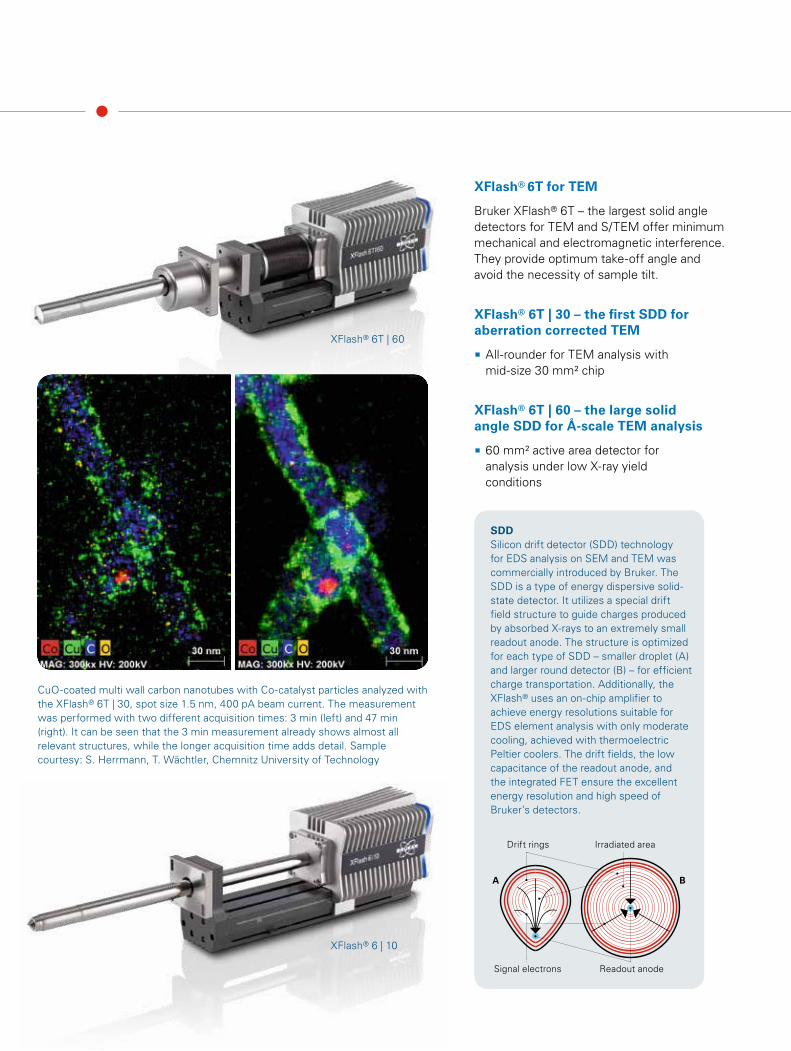
Bruker XFlash® 6T – the largest solid angle detectors for TEM and S/TEM offer minimum mechanical and electromagnetic interference. They provide optimum take-off angle and avoid the necessity of sample tilt.
XFlash® 6T | 30 – the first SDD for aberration corrected TEM
� All-rounder for TEM analysis with mid-size 30 mm² chip
XFlash® 6T | 60 – the large solid angle SDD for Å-scale TEM analysis
� 60 mm² active area detector for analysis under low X-ray yield conditions
CuO-coated multi wall carbon nanotubes with Co-catalyst particles analyzed with the XFlash® 6T | 30, spot size 1.5 nm, 400 pA beam current. The measurement was performed with two different acquisition times: 3 min (left) and 47 min (right). It can be seen that the 3 min measurement already shows almost all relevant structures, while the longer acquisition time adds detail. Sample courtesy: S. Herrmann, T. Wächtler, Chemnitz University of Technology
XFlash® 6T for TEM
SDDSilicon drift detector (SDD) technology for EDS analysis on SEM and TEM was commercially introduced by Bruker. The SDD is a type of energy dispersive solid-state detector. It utilizes a special drift field structure to guide charges produced by absorbed X-rays to an extremely small readout anode. The structure is optimized for each type of SDD – smaller droplet (A) and larger round detector (B) – for efficient charge transportation. Additionally, the XFlash® uses an on-chip amplifier to achieve energy resolutions suitable for EDS element analysis with only moderate cooling, achieved with thermoelectric Peltier coolers. The drift fields, the low capacitance of the readout anode, and the integrated FET ensure the excellent energy resolution and high speed of Bruker’s detectors.
XFlash® 6 | 10
XFlash® 6T | 60
A B
Drift rings Irradiated area
Signal elec trons Readout anode
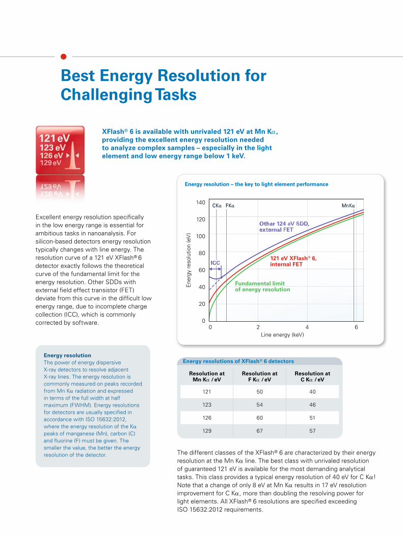
Best Energy Resolution for Challenging Tasks
XFlash® 6 is available with unrivaled 121 eV at Mn Ka, providing the excellent energy resolution needed to analyze complex samples – especially in the light element and low energy range below 1 keV.
Energy resolution – the key to light element performanceEn
ergy
reso
lutio
n (e
V)
Line energy (keV)0
0
20
40
60
80
100
140
120
2 4 6
121 eV XFlash® 6, internal FET
Fundamental limit of energy resolution
ICCICCCCCCCC
C KαCCCCKKKKαC Kα F KαFFFKKKKαF Kα Mn KαMMMMnnKαMn Kα
Other 124 eV SDD, external FETOther 124 eVeV SDDDD,externnal FEET
Resolution at Mn Ka / eV
Resolution at F Ka / eV
Resolution at C Ka / eV
121 50 40
123 54 46
126 60 51
129 67 57
Energy resolutions of XFlash® 6 detectors
Excellent energy resolution specifically in the low energy range is essential for ambitious tasks in nanoanalysis. For silicon-based detectors energy resolution typically changes with line energy. The resolution curve of a 121 eV XFlash® 6
detector exactly follows the theoretical curve of the fundamental limit for the energy resolution. Other SDDs with external field effect transistor (FET) deviate from this curve in the difficult low energy range, due to incomplete charge collection (ICC), which is commonly corrected by software.
The different classes of the XFlash® 6 are characterized by their energy resolution at the Mn Ka line. The best class with unrivaled resolution of guaranteed 121 eV is available for the most demanding analytical tasks. This class provides a typical energy resolution of 40 eV for C Ka! Note that a change of only 8 eV at Mn Ka results in 17 eV resolution improvement for C Ka, more than doubling the resolving power for light elements. All XFlash® 6 resolutions are specified exceeding ISO 15632:2012 requirements.
Energy resolutionThe power of energy dispersive X-ray detectors to resolve adjacent X-ray lines. The energy resolution is commonly measured on peaks recorded from Mn Ka radiation and expressed in terms of the full width at half maximum (FWHM). Energy resolutions for detectors are usually specified in accordance with ISO 15632:2012, where the energy resolution of the Ka peaks of manganese (Mn), carbon (C) and fluorine (F) must be given. The smaller the value, the better the energy resolution of the detector.
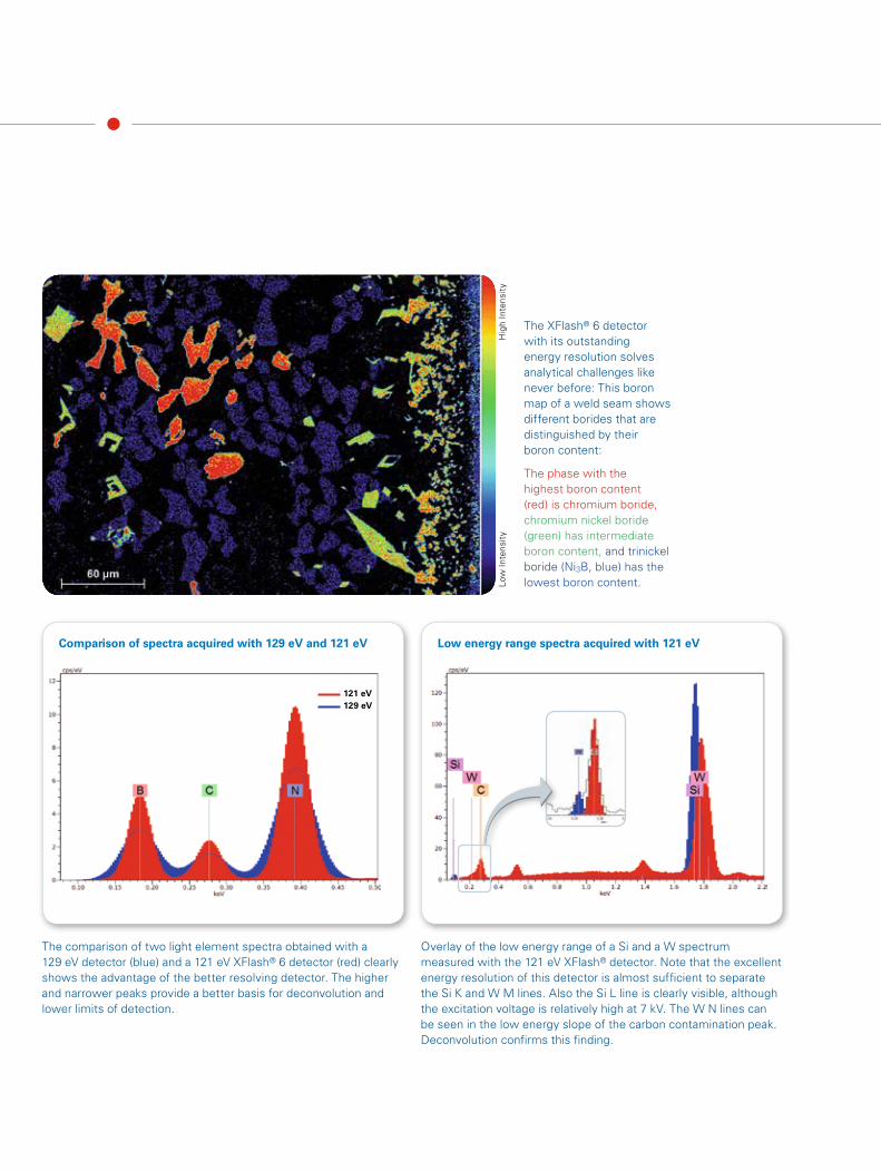
The XFlash® 6 detector with its outstanding energy resolution solves analytical challenges like never before: This boron map of a weld seam shows different borides that are distinguished by their boron content:
The phase with the highest boron content (red) is chromium boride, chromium nickel boride (green) has intermediate boron content, and trinickel boride (Ni3B, blue) has the lowest boron content.
The comparison of two light element spectra obtained with a 129 eV detector (blue) and a 121 eV XFlash® 6 detector (red) clearly shows the advantage of the better resolving detector. The higher and narrower peaks provide a better basis for deconvolution and lower limits of detection.
Overlay of the low energy range of a Si and a W spectrum measured with the 121 eV XFlash® detector. Note that the excellent energy resolution of this detector is almost sufficient to separate the Si K and W M lines. Also the Si L line is clearly visible, although the excitation voltage is relatively high at 7 kV. The W N lines can be seen in the low energy slope of the carbon contamination peak. Deconvolution confirms this finding.
Comparison of spectra acquired with 129 eV and 121 eV Low energy range spectra acquired with 121 eV
121 eV129 eV
Hig
h In
tens
ity
Low
Inte
nsit
y
Fast and accurate
� Noise free sensor supply
� Precise temperature control
� Ultra high throughput
� Optimum energy resolution
� Automatic operation (user control optional)
Versatile and safe
� Support of up to four detectors in one system
� Separate slider control for each detector
� Hardware and software interlock for safe detector operation
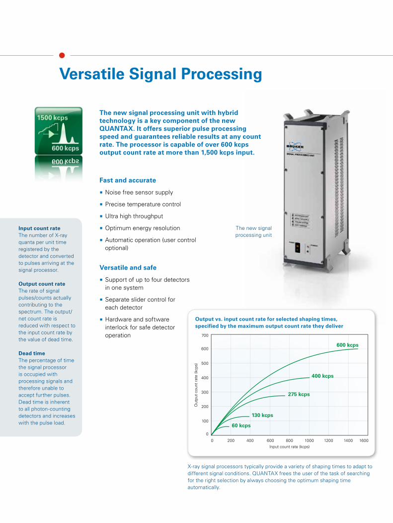
Versatile Signal Processing
The new signal processing unit with hybrid technology is a key component of the new QUANTAX. It offers superior pulse processing speed and guarantees reliable results at any count rate. The processor is capable of over 600 kcps output count rate at more than 1,500 kcps input.
X-ray signal processors typically provide a variety of shaping times to adapt to different signal conditions. QUANTAX frees the user of the task of searching for the right selection by always choosing the optimum shaping time automatically.
Output vs. input count rate for selected shaping times, specified by the maximum output count rate they deliver
Out
put c
ount
rate
(kcp
s)
Input count rate (kcps)0 400 800 1200 1600200 600 1000 1400
700
600
500
400
300
200
100
0
600 kcps
400 kcps
275 kcps
130 kcps
60 kcps
Input count rateThe number of X-ray quanta per unit time registered by the detector and converted to pulses arriving at the signal processor.
Output count rateThe rate of signal pulses/counts actually contributing to the spectrum. The output/net count rate is reduced with respect to the input count rate by the value of dead time.
Dead timeThe percentage of time the signal processor is occupied with processing signals and therefore unable to accept further pulses. Dead time is inherent to all photon-counting detectors and increases with the pulse load.
The new signal processing unit
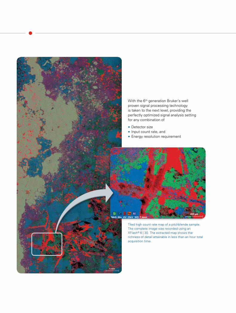
Tiled high count rate map of a pitchblende sample. The complete image was recorded using an XFlash® 6 | 30. The extracted map shows the richness of detail attainable in less than an hour total acquisition time.
With the 6th generation Bruker’s well proven signal processing technology is taken to the next level, providing the perfectly optimized signal analysis setting for any combination of
� Detector size � Input count rate, and � Energy resolution requirement
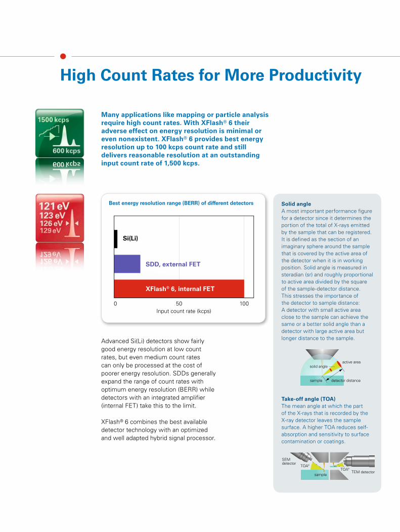
Advanced Si(Li) detectors show fairly good energy resolution at low count rates, but even medium count rates can only be processed at the cost of poorer energy resolution. SDDs generally expand the range of count rates with optimum energy resolution (BERR) while detectors with an integrated amplifier (internal FET) take this to the limit.
XFlash® 6 combines the best available detector technology with an optimized and well adapted hybrid signal processor.
Solid angleA most important performance figure for a detector since it determines the portion of the total of X-rays emitted by the sample that can be registered. It is defined as the section of an imaginary sphere around the sample that is covered by the active area of the detector when it is in working position. Solid angle is measured in steradian (sr) and roughly proportional to active area divided by the square of the sample-detector distance. This stresses the importance of the detector to sample distance: A detector with small active area close to the sample can achieve the same or a better solid angle than a detector with large active area but longer distance to the sample.
Take-off angle (TOA)The mean angle at which the part of the X-rays that is recorded by the X-ray detector leaves the sample surface. A higher TOA reduces self-absorption and sensitivity to surface contamination or coatings.
sample
TOA°
SEM detector
TOA°TEM detector
High Count Rates for More Productivity
Many applications like mapping or particle analysis require high count rates. With XFlash® 6 their adverse effect on energy resolution is minimal or even nonexistent. XFlash® 6 provides best energy resolution up to 100 kcps count rate and still delivers reasonable resolution at an outstanding input count rate of 1,500 kcps.
sample
active area
detector distance
solid angle
Best energy resolution range (BERR) of different detectors
Input count rate (kcps)0 50 100
XFlash® 6, internal FET
SDD, external FET
Si(Li)
Slim-line technology means ultra-thin detector fingers, providing
� Maximized solid angle
� Clearance of other detectors
� Optimized take-off angle
Advantages of compact and light-weight design
� Minimal interference on the electron microscope
� Reduced weight of less than 3.75 kg
� Reduced overall height
� New high precision motorized slider
� Exact repositioning of the detector
� New larger surface area heat sink
� Optionally available with welded bellows (standard for XFlash® 6T)
Maximum measurement flexibility through VZ (variable Z)-Adapter
� Tilt and move the detector into the optimum working distance
� Maximized solid angle and count rate
� Optimized in-situ adjustment of combined EDS and EBSD measurements
Slim-line, Compact and Flexible
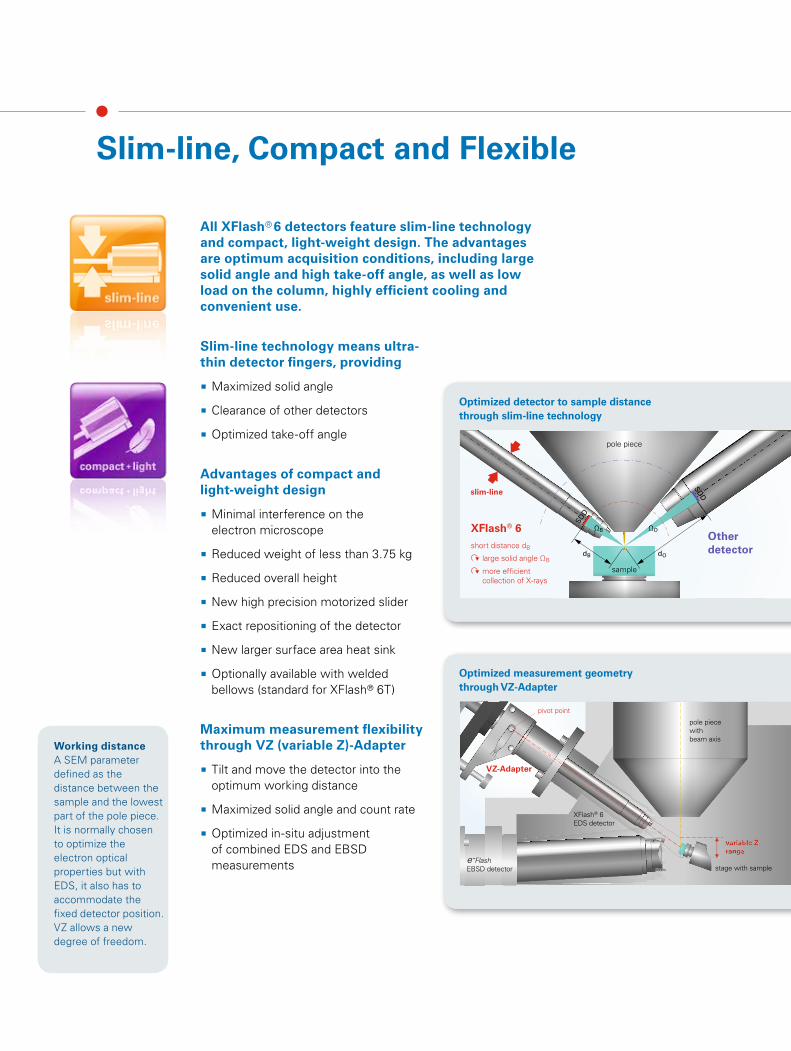
All XFlash® 6 detectors feature slim-line technology and compact, light-weight design. The advantages are optimum acquisition conditions, including large solid angle and high take-off angle, as well as low load on the column, highly efficient cooling and convenient use.
Optimized detector to sample distance through slim-line technology
sample
pole piece
dB dO
slim-line
XFlash® 6short distance dB
large solid angle ΩB
more efficient collection of X-rays
Other detector
SDD
ΩOΩB
SDD
Optimized measurement geometry through VZ-Adapter
XFlash® 6EDS detector
pivot point
VZ-Adapter
variable Z rangevariiable ZZrangge
e-FlashEBSD detector
pole piece with beam axis
stage with sample
Working distanceA SEM parameter defined as the distance between the sample and the lowest part of the pole piece. It is normally chosen to optimize the electron optical properties but with EDS, it also has to accommodate the fixed detector position. VZ allows a new degree of freedom.
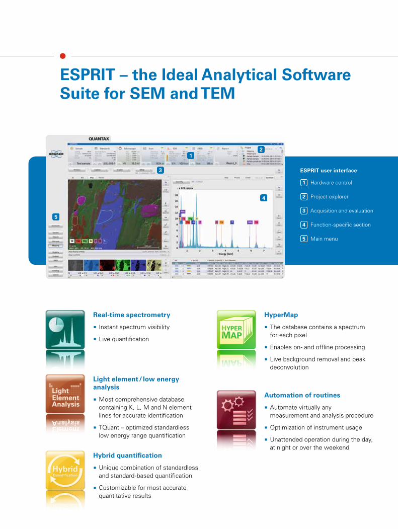
1 Hardware control
2 Project explorer
3 Acquisition and evaluation
4 Function-specific section
5 Main menu
ESPRIT user interface
12
3
4
5
ESPRIT – the Ideal Analytical Software Suite for SEM and TEM
Real-time spectrometry
� Instant spectrum visibility
� Live quantification
Light element / low energy analysis
� Most comprehensive database containing K, L, M and N element lines for accurate identification
� TQuant – optimized standardless low energy range quantification
Hybrid quantification
� Unique combination of standardless and standard-based quantification
� Customizable for most accurate quantitative results
HyperMap
� The database contains a spectrum for each pixel
� Enables on- and offline processing
� Live background removal and peak deconvolution
Automation of routines
� Automate virtually any measurement and analysis procedure
� Optimization of instrument usage
� Unattended operation during the day, at night or over the weekend
Every analysis begins with the selection of the point or area of interest. The QUANTAX real-time spectrometry capabilities facilitate this process. In the preview mode the spectrum is updated at intervals down to 100 milliseconds. The user can easily recognize changes in the spectrum as the measurement spot is moved across the sample.
Live quantification
While the acquisition is running, ESPRIT can perform live quantification and update results as statistics improve. Everything is done automatically, but if desired, intermediate results can be reviewed or quantification can be done interactively.
Taking advantage of the new XFlash® 6 detectors’ speed, the real-time spectrometry function offers instant information on local sample characteristics.
Real-Time Spectrometry – See Composition Changes Immediately
Spectrometry is supported by ...
� Automatic or user controlled acquisition
� Automatic or manual element identification
� Accurate background fitting
� Peak deconvolution using either peak fitting or probability theory based approaches
� State-of-the-art quantification routines
P/B-ZAFFundamental parameter quantitative analysis, based on evaluating characteristic X-rays (peaks) as well as bremsstrahlung background. The local peak to background (P/B) ratios are input to a modified ZAF matrix correction. The P/B-ZAF analysis is self-calibrating. Because characteristic X-rays and bremsstrahlung undergo the same absorption, P/B-ZAF is relatively insensitive to local sample tilt and the surface condition of the specimen.
Matrix correctionAlgorithm that relates the recorded spectrum to the primary rate of X-ray generation. Matrix correction takes into account atomic number effects (Z), absorption effects (A) and secondary fluorescence effects (F).
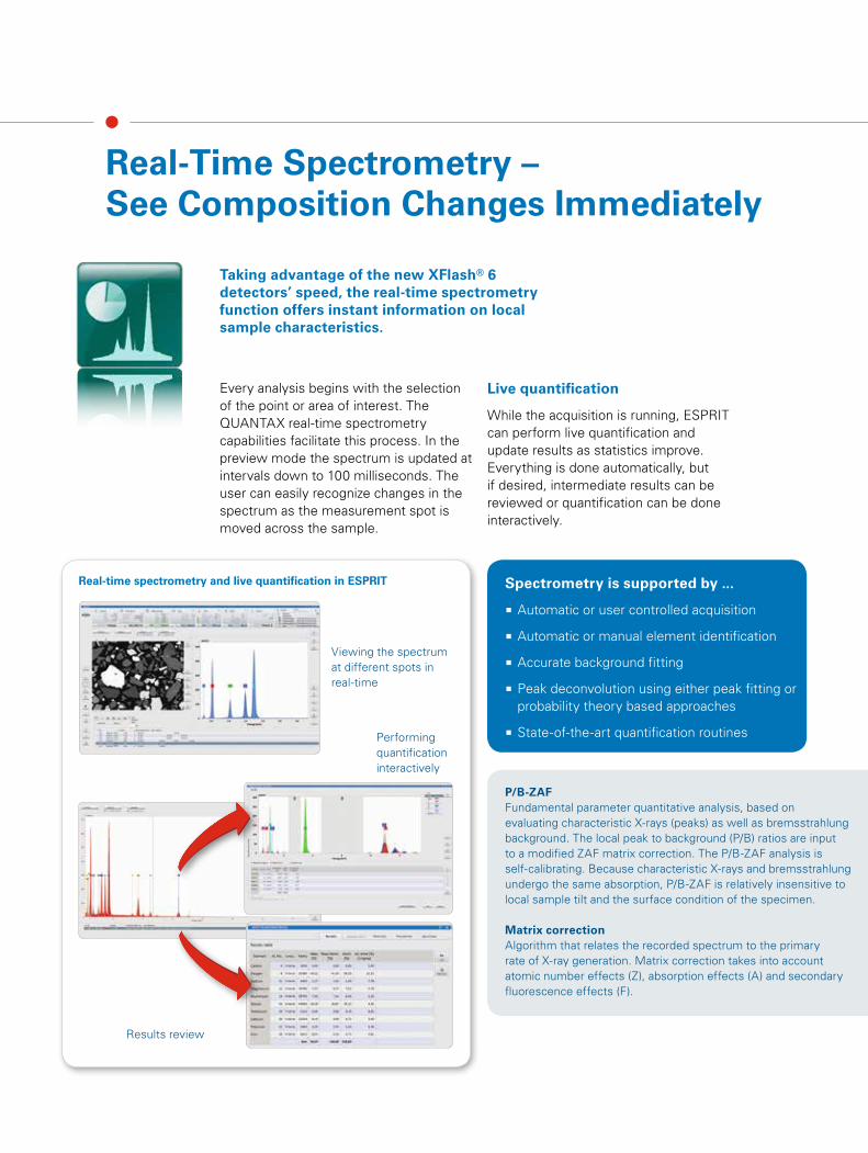
Real-time spectrometry and live quantification in ESPRIT
Results review
Performing quantification interactively
Viewing the spectrum at different spots in real-time
Unsurpassed Light Element and Low Energy Analysis
Correct element identification based on the most comprehensive atomic database
Bruker continuously updates the ESPRIT atomic database, adding further lines and improving accuracy of line energies and intensities. The result is the most comprehensive atomic database containing all confirmed K, L, M and N lines of all elements that can be analyzed with EDS, enabling reliable element identification even at low energies.
TQuant for accurate standardless results
The TQuant standardless low energy quantification procedure provides excellent results. It is now possible to perform reliable quantitative EDS analysis not only in the light element / low energy range but also with spatial resolution at the nanometer scale. Low beam energies in the electron microscope, which produce only small excitation volumes, can now be safely used for quantitative analysis.
Producing reliable analytical results is a challenge, especially at low X-ray energies. Building on the excellent low energy performance of the XFlash® detectors, the ESPRIT software contains several features supporting nanoanalysis in the light element / low energy range.
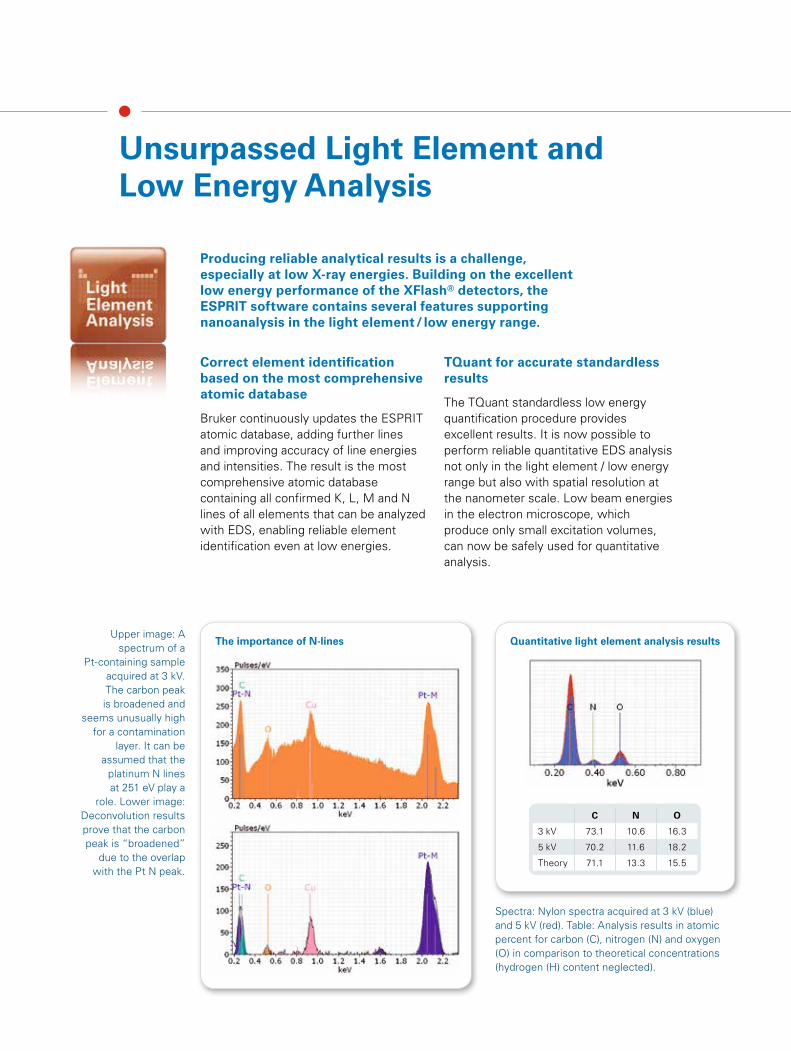
Spectra: Nylon spectra acquired at 3 kV (blue) and 5 kV (red). Table: Analysis results in atomic percent for carbon (C), nitrogen (N) and oxygen (O) in comparison to theoretical concentrations (hydrogen (H) content neglected).
The importance of N-lines Quantitative light element analysis results
C N O
3 kV 73.1 10.6 16.3
5 kV 70.2 11.6 18.2
Theory 71.1 13.3 15.5
Upper image: A spectrum of a
Pt-containing sample acquired at 3 kV. The carbon peak is broadened and
seems unusually high for a contamination
layer. It can be assumed that the
platinum N lines at 251 eV play a
role. Lower image: Deconvolution results prove that the carbon peak is “broadened”
due to the overlap with the Pt N peak.
Φ(ρz)A matrix correction formalism based on mathematical expressions for the ionization depth distribution function (Φ) in relation to mass density (ρ) and the depth of X-ray origin in the sample (z).
XPP (eXtended Pouchou & Pichoir)
A specific Φ(ρz) correction method developed by Jean-Louis Pouchou and Francoise Pichoir.
Cliff-LorimerThis quantification method relates the measured peak intensities to calculated or measured intensities of standards. It can be applied for systems where absorption or fluorescence effects can be neglected, which is normally the case for thin samples as analyzed in TEMs.
While using the true standardless quantification as default method, the standard-based analysis can be assigned to elements for which reference standards are available. This provides the most reliable and precise quantification possible.
Standardless and standard-based quantitative analysis are both common in the world of X-ray spectrometry. Bruker’s unique hybrid quantification is the customizable combination of both.
Hybrid Quantification for Maximum Accuracy
ESPRIT uses the most advanced methods for quantification
� True standardless P/B-ZAF for rough and polished surfaces and true standardless Φ(ρz) with XPP matrix correction
� Standard-based P/B-ZAF and standard-based Φ(ρz) with XPP matrix correction
� Cliff-Lorimer quantification for TEM and thin samples, both standardless and standard-based
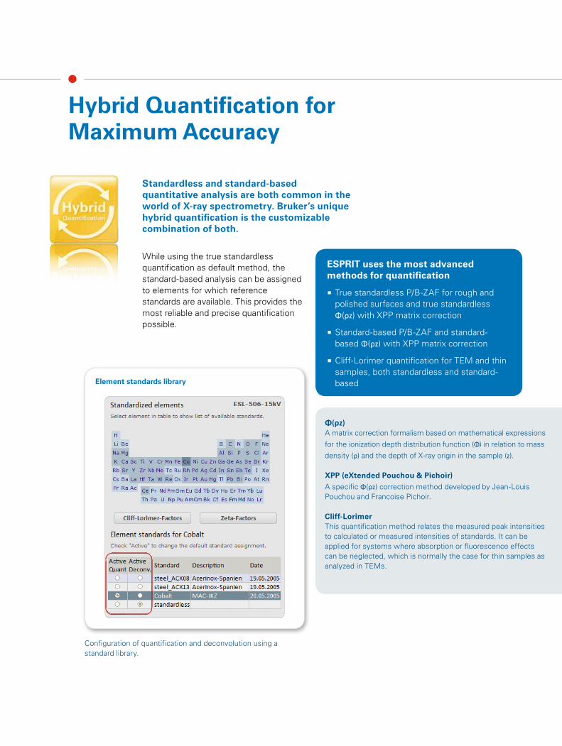
Configuration of quantification and deconvolution using a standard library.
Element standards library
HyperMap allows acquiring an advanced type of element map, in which a complete spectrum is stored for every pixel in the map. The collected database, or spectrum image, permits further processing and analysis of the data at any time during or after the measurement.
Processing tools include extracting, quantifying and comparing EDS spectra of selected regions in the map, calculating a Maximum Pixel Spectrum, obtaining line scans, displaying a map for any element, as well as automatic phase analysis.
ESPRIT HyperMap is one of the most versatile tools for EDS analysis. Select an area of interest, set up the acquisition, collect a map – even without any prior knowledge of sample composition – and analyze it offline.
HyperMap – Measure First, Analyze Later
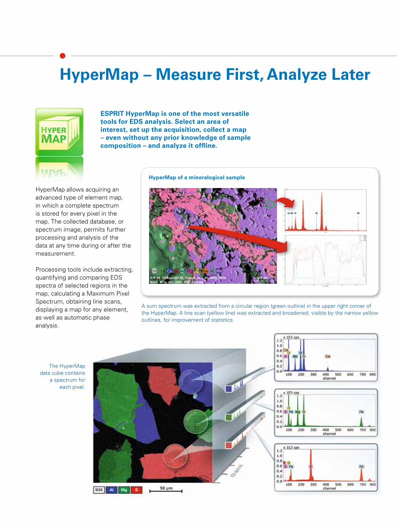
HyperMap of a mineralogical sample
A sum spectrum was extracted from a circular region (green outline) in the upper right corner of the HyperMap. A line scan (yellow line) was extracted and broadened, visible by the narrow yellow outlines, for improvement of statistics.
The HyperMap data cube contains
a spectrum for each pixel.
ColorScanDuring scanning the image is displayed in color by combining X-ray and electron information in real-time. ColorScan provides instant qualitative information on sample composition, homogeneity and even on different phases.
Maximum Pixel Spectrum – the perfect tool for trace analysis
The highest count rate recorded in each energy channel, for each pixel in the map, is displayed in a synthesized spectrum. If a certain element has a high concentration, the corresponding peak becomes visible in the Maximum Pixel Spectrum, even if this element is present in only a single pixel of the map.
Phase analysis using Autophase
ESPRIT’s Autophase function determines the present chemical phases using an automated principle components analysis (PCA) algorithm. The conditions for analysis are either set by different thresholds (automatically or manually) or by defining objects in a map.
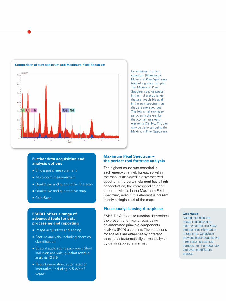
Comparison of sum spectrum and Maximum Pixel Spectrum
Comparison of a sum spectrum (blue) and a Maximum Pixel Spectrum (red) of a granite sample. The Maximum Pixel Spectrum shows peaks in the mid energy range that are not visible at all in the sum spectrum, as they are averaged out. The few small monazite particles in the granite, that contain rare earth elements (Ce, Nd, Th), can only be detected using the Maximum Pixel Spectrum.
Further data acquisition and analysis options
� Single point measurement
� Multi-point measurement
� Qualitative and quantitative line scan
� Qualitative and quantitative map
� ColorScan
ESPRIT offers a range of advanced tools for data processing and reporting
� Image acquisition and editing
� Feature analysis, including chemical classification
� Special applications packages: Steel inclusion analysis, gunshot residue analysis (GSR)
� Report generation, automated or interactive, including MS Word® export
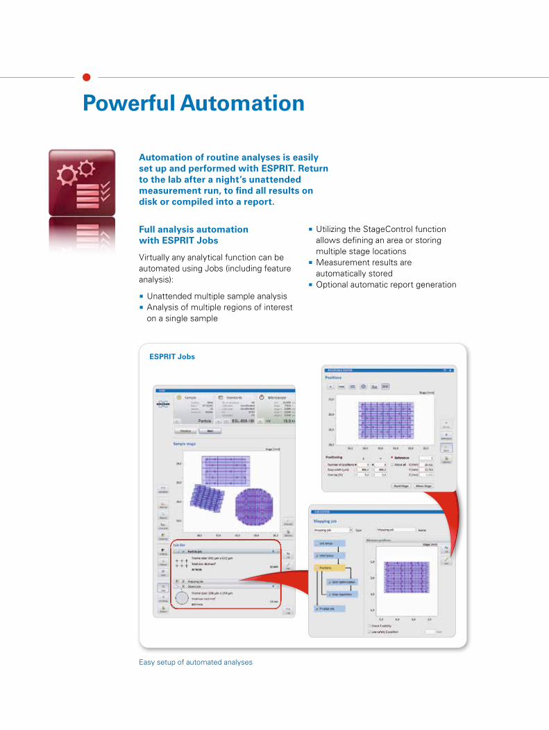
Full analysis automation with ESPRIT Jobs
Virtually any analytical function can be automated using Jobs (including feature analysis):
� Unattended multiple sample analysis � Analysis of multiple regions of interest on a single sample
� Utilizing the StageControl function allows defining an area or storing multiple stage locations
� Measurement results are automatically stored
� Optional automatic report generation
Automation of routine analyses is easily set up and performed with ESPRIT. Return to the lab after a night’s unattended measurement run, to find all results on disk or compiled into a report.
ESPRIT Jobs
Easy setup of automated analyses
Powerful Automation
Analysis Method Coupling
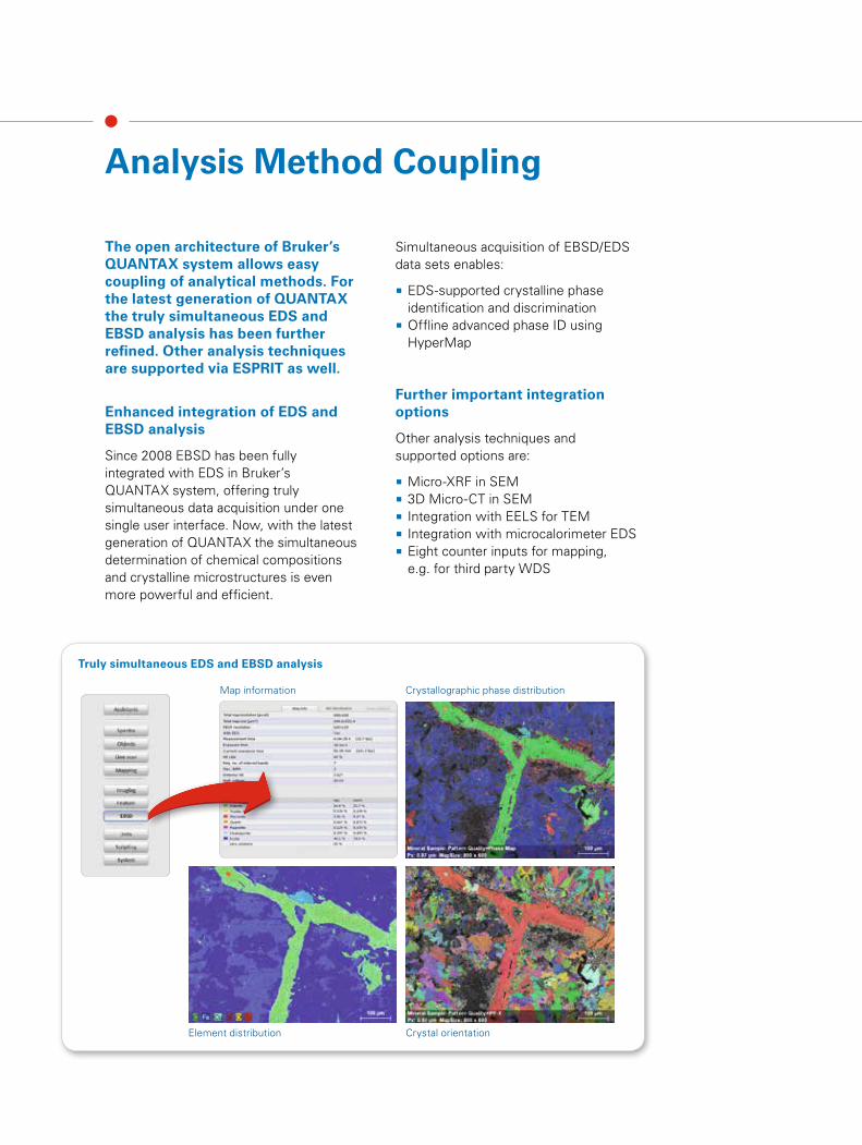
The open architecture of Bruker’s QUANTAX system allows easy coupling of analytical methods. For the latest generation of QUANTAX the truly simultaneous EDS and EBSD analysis has been further refined. Other analysis techniques are supported via ESPRIT as well.
Enhanced integration of EDS and EBSD analysis
Since 2008 EBSD has been fully integrated with EDS in Bruker’s QUANTAX system, offering truly simultaneous data acquisition under one single user interface. Now, with the latest generation of QUANTAX the simultaneous determination of chemical compositions and crystalline microstructures is even more powerful and efficient.
Simultaneous acquisition of EBSD/EDS data sets enables:
� EDS-supported crystalline phase identification and discrimination
� Offline advanced phase ID using HyperMap
Further important integration options
Other analysis techniques and supported options are:
� Micro-XRF in SEM � 3D Micro-CT in SEM � Integration with EELS for TEM � Integration with microcalorimeter EDS � Eight counter inputs for mapping, e.g. for third party WDS
Truly simultaneous EDS and EBSD analysis
Crystallographic phase distribution
Element distribution Crystal orientation
Map information
Specifications
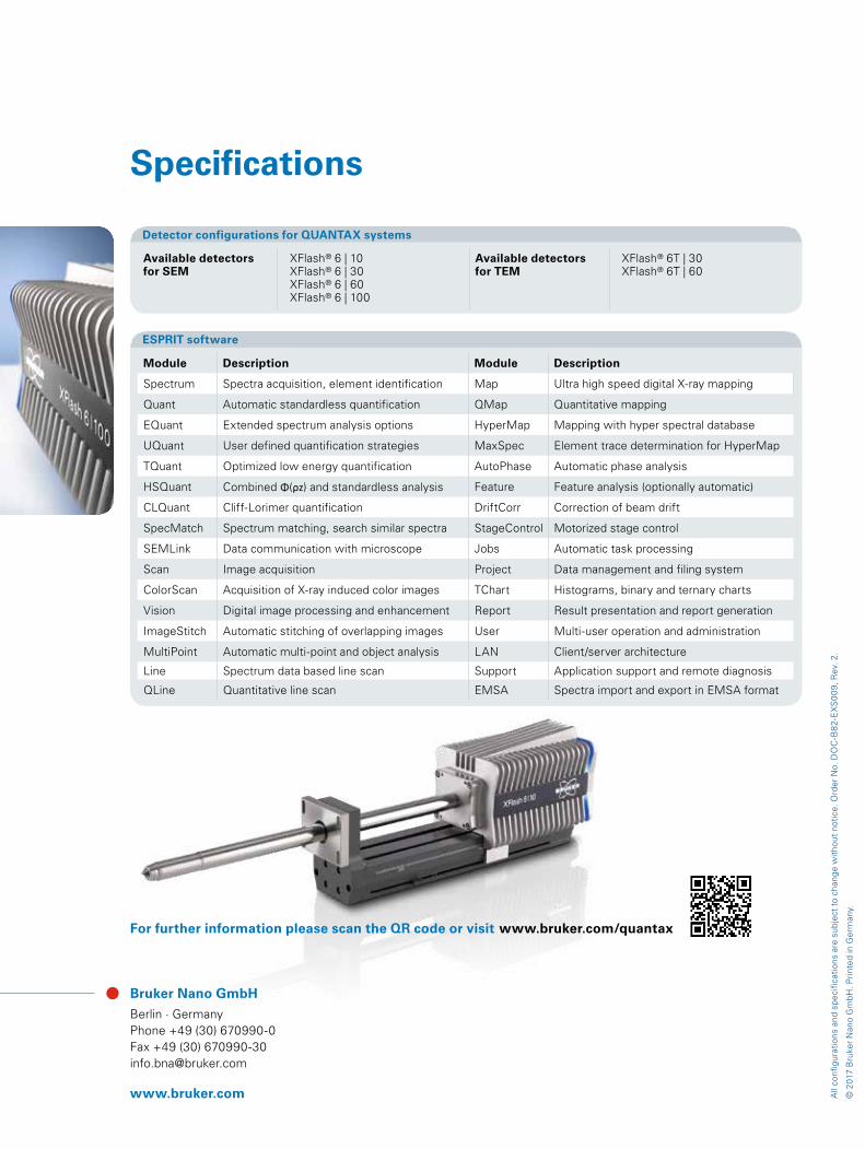
Available detectors for SEM
XFlash® 6 | 10 XFlash® 6 | 30 XFlash® 6 | 60 XFlash® 6 | 100
Available detectors for TEM
XFlash® 6T | 30 XFlash® 6T | 60
Detector configurations for QUANTAX systems
Module Description Module Description
Spectrum Spectra acquisition, element identification Map Ultra high speed digital X-ray mapping
Quant Automatic standardless quantification QMap Quantitative mapping
EQuant Extended spectrum analysis options HyperMap Mapping with hyper spectral database
UQuant User defined quantification strategies MaxSpec Element trace determination for HyperMap
TQuant Optimized low energy quantification AutoPhase Automatic phase analysis
HSQuant Combined Φ(ρz) and standardless analysis Feature Feature analysis (optionally automatic)
CLQuant Cliff-Lorimer quantification DriftCorr Correction of beam drift
SpecMatch Spectrum matching, search similar spectra StageControl Motorized stage control
SEMLink Data communication with microscope Jobs Automatic task processing
Scan Image acquisition Project Data management and filing system
ColorScan Acquisition of X-ray induced color images TChart Histograms, binary and ternary charts
Vision Digital image processing and enhancement Report Result presentation and report generation
ImageStitch Automatic stitching of overlapping images User Multi-user operation and administration
MultiPoint Automatic multi-point and object analysis LAN Client/server architecture
Line Spectrum data based line scan Support Application support and remote diagnosis
QLine Quantitative line scan EMSA Spectra import and export in EMSA format
ESPRIT software
For further information please scan the QR code or visit www.bruker.com/quantax
Bruker Nano GmbH
Berlin · GermanyPhone +49 (30) 670990-0 Fax +49 (30) 670990-30 [email protected]
www.bruker.com All
conf
igur
atio
ns a
nd s
peci
ficat
ions
are
sub
ject
to
chan
ge w
ithou
t no
tice.
Ord
er N
o. D
OC
-B82
-EX
S0
09,
Rev
. 2.
© 2
017
Bru
ker
Nan
o G
mbH
. Prin
ted
in G
erm
any.