q q - dynfperal/cursos-anteriores/05-06/... · e l e m e n t o d e m e m o r i a c o n d o s i n v...
TRANSCRIPT

Cir
cuito
s se
cuen
cial
es
CO
MB
INA
CIO
NA
L
ME
MO
RIA
EN
TR
AD
AS
SA
LID
AS
CO
MB
INA
CIO
NA
L
ME
MO
RIA
EN
TR
AD
AS
SA
LID
AS
CO
MB
INA
CIO
NA
L
ME
AL
Y
MO
OR
E
CL
AS
IFIC
AC
IÓN
Se
gún
la
estr
uctu
ra»
Moo
re»
Mea
ly
Segú
n la
ev
oluc
ión
»S
íncr
onos
Por
niv
el
Por
fla
nco
»A
sínc
rono
s
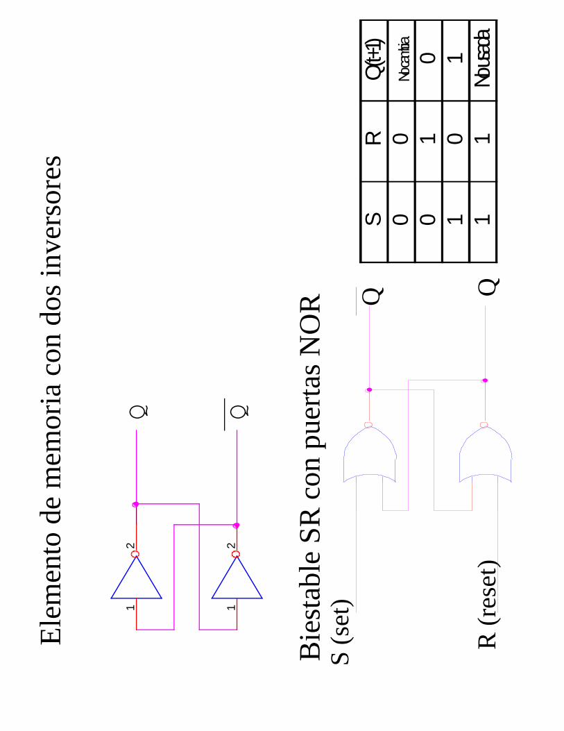
Ele
men
to d
e m
emor
ia c
on d
os in
vers
ores
Q Q
12
12
Bie
stab
le S
R c
on p
uert
as N
OR
S (s
et)
R (
rese
t)
Q Q
SR
Q (t+
1)0
0No
camb
ia
01
01
01
11
No us
ada

Bie
stab
les
RS
S (s
et)
R (
rese
t)Q Q
S (s
et)
R (
rese
t)Q Q


RS
con
PR y
CL
y f
lip−
flop
mas
ter−
slav
e
RSQ Q
CL
K
PR
(pr
eset
)
CL
(cl
ear)
R SQ Q
QS
QR
R S
CL
K
Q Q

BIESTABLE D LATCH SÍNCRONO
BIESTABLE JK LATCH SÍNCRONO


Aes
tabl
es
12
12
12
12
RR
s

T=
1’2
RC
Aes
tabl
e co
n ne
gado
r tr
igge
r sc
hmitt

Mon
oest
able
s
Dis
paro
Vdd
Dis
paro
Vdd
C2
R1
C1
R2

Mon
oest
able
con
741
21
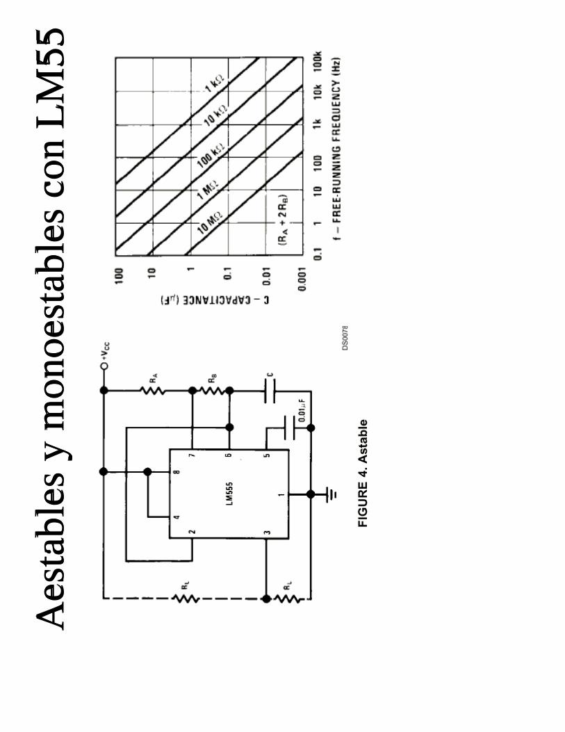
Aes
tabl
es y
mon
oest
able
s co
n L
M55


TL/F/6538
54121/D
M54121/D
M74121
One-S
hotw
ithC
learand
Com
ple
menta
ryO
utp
uts
June 1989
54121/DM54121/DM74121 One-Shot withClear and Complementary Outputs
General DescriptionThe DM54/74121 is a monostable multivibrator featuring
both positive and negative edge triggering with complemen-
tary outputs. An internal 2kX timing resistor is provided for
design convenience minimizing component count and lay-
out problems. This device can be used with a single external
capacitor. Inputs (A) are active-low trigger transition inputs
and input (B) is an active-high transition Schmitt-trigger in-
put that allows jitter-free triggering from inputs with tran-
sition rates as slow as 1 volt/second. A high immunity to
VCC noise of typically 1.5V is also provided by internal cir-
cuitry at the input stage.
To obtain optimum and trouble free operation please read
operating rules and NSC one-shot application notes careful-
ly and observe recommendations.
FeaturesY Triggered from active-high transition or active-low tran-
sition inputsY Variable pulse width from 30 ns to 28 seconds
Y Jitter free Schmitt-trigger inputY Excellent noise immunity typically 1.2VY Stable pulse width up to 90% duty cycleY TTL, DTL compatibleY Compensated for VCC and temperature variationsY Input clamp diodesY Alternate Military/Aerospace device (54121) is avail-
able. Contact a National Semiconductor Sales Office/
Distributor for specifications.
Functional DescriptionThe basic output pulse width is determined by selection of
an internal resistor RINT or an external resistor (RX) and
capacitor (CX). Once triggered the output pulse width is in-
dependent of further transitions of the inputs and is a func-
tion of the timing components. Pulse width can vary from a
few nano-seconds to 28 seconds by choosing appropriate
RX and CX combinations. There are three trigger inputs from
the device, two negative edge-triggering (A) inputs, one pos-
itive edge Schmitt-triggering (B) input.
Connection Diagram
Dual-In-Line Package
TL/F/6538–1
Order Number 54121DMQB, 54121FMQB,
DM54121J, DM54121W or DM74121N
See NS Package Number J14A, N14A or W14B
Function Table
Inputs Outputs
A1 A2 B Q Q
L X H L H
X L H L H
X X L L H
H H X L H
H v H É ß
v H H É ß
v v H É ßL X u É ßX L u É ß
H e High Logic Level
L e Low Logic Level
X e Can Be Either Low or High
u e Positive Going Transition
v e Negative Going Transition
É e A Positive Pulse
ß e A Negative Pulse
C1995 National Semiconductor Corporation RRD-B30M105/Printed in U. S. A.

Absolute Maximum Ratings (Note)
If Military/Aerospace specified devices are required,
please contact the National Semiconductor Sales
Office/Distributors for availability and specifications.
Supply Voltage 7V
Input Voltage 5.5V
Operating Free Air Temperature Range
DM54 b55§C to a125§CDM74 0§C to a70§C
Storage Temperature Range b65§C to a150§C
Note: The ‘‘Absolute Maximum Ratings’’ are those valuesbeyond which the safety of the device cannot be guaran-teed. The device should not be operated at these limits. Theparametric values defined in the ‘‘Electrical Characteristics’’table are not guaranteed at the absolute maximum ratings.The ‘‘Recommended Operating Conditions’’ table will definethe conditions for actual device operation.
Recommended Operating Conditions
Symbol ParameterDM54121 DM74121
UnitsMin Nom Max Min Nom Max
VCC Supply Voltage 4.5 5 5.5 4.75 5 5.25 V
VTa Positive-Going Input Threshold1.4 2 1.4 2 V
Voltage at the A Input (VCC e Min)
VTb Negative-Going Input Threshold0.8 1.4 0.8 1.4 V
Voltage at the A Input (VCC e Min)
VTa Positive-Going Input Threshold1.5 2 1.5 2 V
Voltage at the B Input (VCC e Min)
VTb Negative-Going Input Threshold0.8 1.3 0.8 1.3 V
Voltage at the B Input (VCC e Min)
IOH High Level Output Current b0.4 b0.4 mA
IOL Low Level Output Current 16 16 mA
tW Input Pulse Width (Note 1) 40 40 ns
dV/dtRate of Rise or Fall of
1 1 V/sSchmidt Input (B) (Note 1)
dV/dtRate of Rise or Fall of
1 1 V/msLogic Input (A) (Note 1)
REXT External Timing Resistor (Note 1) 1.4 30 1.4 40 kX
CEXT External Timing Capacitance (Note 1) 0 1000 0 1000 mF
DC Duty Cycle (Note 1) RT e 2 kX 67 67%
RT e REXT (Max) 90 90
TA Free Air Operating Temperature b55 125 0 70 §CNote 1: TA e 25§C and VCC e 5V.
Electrical Characteristics over recommended operating free air temperature range (unless otherwise noted)
Symbol Parameter Conditions MinTyp
Max Units(Note 1)
VI Input Clamp Voltage VCC e Min, II e b12 mA b1.5 V
VOH High Level Output VCC e Min, IOH e Max,2.4 3.4 V
Voltage VIL e Max, VIH e Min
VOL Low Level Output VCC e Min, IOL e Max,0.2 0.4 V
Voltage VIH e Min, VIL e Max
II Input Current @ Max VCC e Max, VI e 5.5V1 mA
Input Voltage
IIH High Level Input VCC e Max A1, A2 40mA
Current VI e 2.4V B 80
IIL Low Level Input VCC e Max A1, A2 b1.6mA
Current VI e 0.4V B b3.2
IOS Short Circuit VCC e Max DM54 b20 b55mA
Output Current (Note 2) DM74 b18 b55
ICC Supply Current VCC e Max Quiescent 13 25mA
Triggered 23 40
Note 1: All typicals are at VCC e 5V, TA e 25§C.
Note 2: Not more than one output should be shorted at a time.
2

Switching Characteristics at VCC e 5V and TA e 25§C (See Section 1 for Test Waveforms and Outout Load)
Symbol ParameterFrom (Input)
Conditions Min Max UnitsTo (Output)
tPLH Propagation Delay Time A1, A2 CEXT e 80 pF70 ns
Low to High Level Output to Q RINT to VCC
tPLH Propagation Delay Time B to CL e 15 pF55 ns
Low to High Level Output Q RL e 400X
tPHL Propagation Delay Time A1, A280 ns
High to Low Level Output to Q
tPHL Propagation Delay Time B65 ns
High to Low Level Output to Q
tW(OUT) Output Pulse A1, A2 or B CEXT e 80 pF
Width Using the to Q, Q RINT to VCC 70 150 nsInternal Timing Resistor RL e 400X
CL e 15 pF
tW(OUT) Output Pulse A1, A2 CEXT e 0 pF
Width Using Zero to Q, Q RINT to VCC 50 nsTiming Capacitance RL e 400X
CL e 15 pF
tW(OUT) Output Pulse A1, A2 CEXT e 100 pF
Width Using External to Q, Q RINT e 10 kX600 800 ns
Timing Resistor RL e 400X
CL e 15 pF
A1, A2 CEXT e 1 mF
to Q, Q RINT e 10 kX6 8 ms
RL e 400X
CL e 15 pF
Operating Rules
1. To use the internal 2 kX timing resistor, connect the RINTpin to VCC.
2. An external resistor (RX) or the internal resistor (2 kX)
and an external capacitor (CX) are required for proper
operation. The value of CX may vary from 0 to any neces-
sary value. For small time constants use high-quality
mica, glass, polypropylene, polycarbonate, or polystyrene
capacitors. For large time constants use solid tantalum or
special aluminum capacitors. If the timing capacitors
have leakages approaching 100 nA or if stray capaci-
tance from either terminal to ground is greater than 50 pF
the timing equations may not represent the pulse width
the device generates.
3. The pulse width is essentially determined by external tim-
ing components RX and CX. For CX k 1000 pF see Fig-ure 1 design curves on TW as function of timing compo-
nents value. For CX l1000 pF the output is defined as:
tW e K RX CX
where [RX is in Kilo-ohm][CX is in pico Farad][TW is in nano second][K & 0.7]
TL/F/6538–2
FIGURE 1
4. If CX is an electrolytic capacitor a switching diode is often
required for standard TTL one-shots to prevent high in-
verse leakage current (Figure 2) .
TL/F/6538–3
FIGURE 2
3

Operating Rules (Continued)
5. Output pulse width versus VCC and operation tempera-
tures: Figure 3 depicts the relationship between pulse
width variation versus VCC. Figure 4 depicts pulse width
variation versus ambient temperature.
TL/F/6538–4
FIGURE 3
TL/F/6538–5
FIGURE 4
6. The ‘‘K’’ coefficient is not a constant, but varies as a
function of the timing capacitor CX. Figure 5 details this
characteristic.
TL/F/6538–6
FIGURE 5
7. Under any operating condition CX and RX must be kept
as close to the one-shot device pins as possible to mini-
mize stray capacitance, to reduce noise pick-up, and to
reduce I c R and Ldi/dt voltage developed along their
connecting paths. If the lead length from CX to pins (10)
and (11) is greater than 3 cm, for example, the output
pulse width might be quite different from values predicted
from the appropriate equations. A non-inductive and low
capacitive path is necessary to ensure complete dis-
charge of CX in each cycle of its operation so that the
output pulse width will be accurate.
8. VCC and ground wiring should conform to good high-fre-
quency standards and practices so that switching tran-
sients on the VCC and ground return leads do not cause
interaction between one-shots. A 0.01 mF to 0.10 mF by-
pass capacitor (disk ceramic or monolithic type) from VCCto ground is necessary on each device. Furthermore, the
bypass capacitor should be located as close to the VCC-
pin as space permits.
For further detailed device characteristics and output performance please
refer to the NSC one-shot application note, AN-366.
4

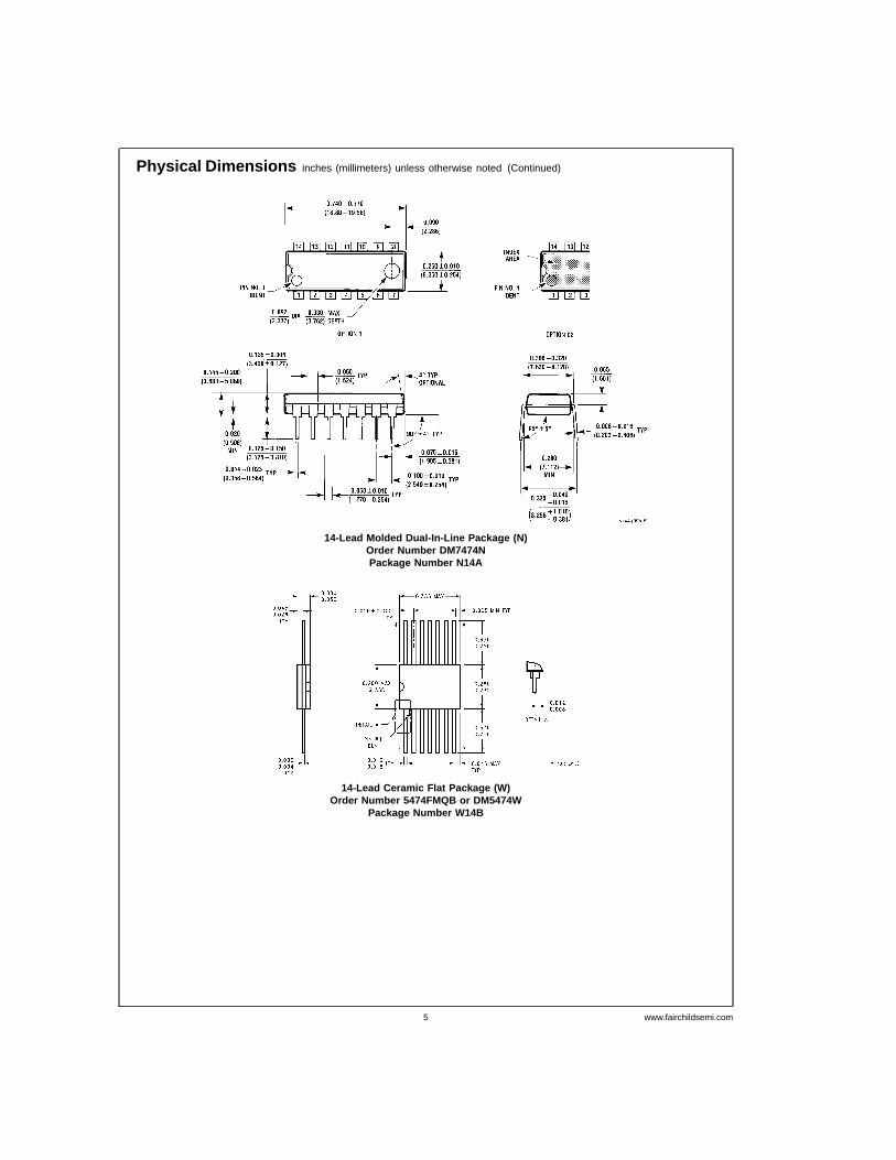
Physical Dimensions inches (millimeters)
14-Lead Ceramic Dual-In-Line Package (J)
Order Number 54121DMQB or DM54121J
NS Package Number J14A
14-Lead Molded Dual-In-Line Package (N)
Order Number DM74121N
NS Package Number N14A
5

54121/D
M54121/D
M74121
One-S
hotw
ith
Cle
arand
Com
ple
menta
ryO
utp
uts
Physical Dimensions inches (millimeters) (Continued)
14-Lead Ceramic Flat Package (W)
Order Number 54121FMQB or DM54121W
NS Package Number W14B
LIFE SUPPORT POLICY
NATIONAL’S PRODUCTS ARE NOT AUTHORIZED FOR USE AS CRITICAL COMPONENTS IN LIFE SUPPORT
DEVICES OR SYSTEMS WITHOUT THE EXPRESS WRITTEN APPROVAL OF THE PRESIDENT OF NATIONAL
SEMICONDUCTOR CORPORATION. As used herein:
1. Life support devices or systems are devices or 2. A critical component is any component of a life
systems which, (a) are intended for surgical implant support device or system whose failure to perform can
into the body, or (b) support or sustain life, and whose be reasonably expected to cause the failure of the life
failure to perform, when properly used in accordance support device or system, or to affect its safety or
with instructions for use provided in the labeling, can effectiveness.
be reasonably expected to result in a significant injury
to the user.
National Semiconductor National Semiconductor National Semiconductor National SemiconductorCorporation Europe Hong Kong Ltd. Japan Ltd.1111 West Bardin Road Fax: (a49) 0-180-530 85 86 13th Floor, Straight Block, Tel: 81-043-299-2309Arlington, TX 76017 Email: cnjwge@ tevm2.nsc.com Ocean Centre, 5 Canton Rd. Fax: 81-043-299-2408Tel: 1(800) 272-9959 Deutsch Tel: (a49) 0-180-530 85 85 Tsimshatsui, KowloonFax: 1(800) 737-7018 English Tel: (a49) 0-180-532 78 32 Hong Kong
Fran3ais Tel: (a49) 0-180-532 93 58 Tel: (852) 2737-1600Italiano Tel: (a49) 0-180-534 16 80 Fax: (852) 2736-9960
National does not assume any responsibility for use of any circuitry described, no circuit patent licenses are implied and National reserves the right at any time without notice to change said circuitry and specifications.

DM7474Dual Positive-Edge-Triggered D Flip-Flops with Preset,Clear and Complementary OutputsGeneral DescriptionThis device contains two independentpositive-edge-triggered D flip-flops with complementary out-puts. The information on the D input is accepted by theflip-flops on the positive going edge of the clock pulse. Thetriggering occurs at a voltage level and is not directly relatedto the transition time of the rising edge of the clock. The dataon the D input may be changed while the clock is low or highwithout affecting the outputs as long as the data setup and
hold times are not violated. A low logic level on the preset orclear inputs will set or reset the outputs regardless of thelogic levels of the other inputs.
Featuresn Alternate Military/Aerospace device (5474) is available.
Contact a Fairchild Semiconductor SalesOffice/Distributor for specifications.
Connection Diagram
Function TableInputs Outputs
PR CLR CLK D Q Q
L H X X H L
H L X X L H
L L X X H(Note 1)
H(Note 1)
H H ↑ H H L
H H ↑ L L H
H H L X Q0 Q0
H = High Logic LevelX = Either Low or High Logic LevelL = Low Logic Level
↑ = Positive-going transition of the clock.
Note 1: This configuration is nonstable; that is, it will not persist when either the preset and/or clear inputs return to their inactive (high) level.
Q0 = The output logic level of Q before the indicated input conditions were established.
Dual-In-Line Package
DS006526-1
Order Number 5474DMQB, 5474FMQB, DM5474J, DM5474W, DM7474M or DM7474NSee Package Number J14A, M14A, N14A or W14B
March 1998
DM
7474D
ualPositive-E
dge-TriggeredD
Flip-Flopsw
ithP
reset,Clear
andC
omplem
entaryO
utputs
© 1998 Fairchild Semiconductor Corporation DS006526 www.fairchildsemi.com

Absolute Maximum Ratings (Note 2)
Supply Voltage 7VInput Voltage 5.5VOperating Free Air Temperature Range
DM54 and 54 −55˚C to +125˚CDM74 0˚C to +70˚C
Storage Temperature Range −65˚C to +150˚C
Recommended Operating Conditions
Symbol Parameter DM5474 DM7474 Units
Min Nom Max Min Nom Max
VCC Supply Voltage 4.5 5 5.5 4.75 5 5.25 V
VIH High Level Input Voltage 2 2 V
VIL Low Level Input Voltage 0.8 0.8 V
IOH High Level Output Current −0.4 −0.4 mA
IOL Low Level Output Current 16 16 mA
fCLK Clock Frequency (Note 4) 0 15 0 15 MHz
tW Pulse Width Clock High 30 30
(Note 4) Clock Low 37 37 ns
Clear Low 30 30
Preset Low 30 30
tSU Input Setup Time (Notes 3, 4) 20↑ 20↑ ns
tH Input Hold Time (Notes 3, 4) 5↑ 5↑ ns
TA Free Air Operating Temperature −55 125 0 70 ˚CNote 2: The “Absolute Maximum Ratings” are those values beyond which the safety of the device cannot be guaranteed. The device should not be operated at theselimits. The parametric values defined in the “Electrical Characteristics” table are not guaranteed at the absolute maximum ratings. The “Recommended OperatingConditions” table will define the conditions for actual device operation.
Note 3: The symbol (↑) indicates the rising edge of the clock pulse is used for reference.
Note 4: TA = 25˚C and VCC = 5V.
Electrical Characteristicsover recommended operating free air temperature range (unless otherwise noted)
Symbol Parameter Conditions Min Typ Max Units
(Note 5)
VI Input Clamp Voltage VCC = Min, II = −12 mA −1.5 V
VOH High Level Output VCC = Min, IOH = Max 2.4 3.4 V
Voltage VIL = Max, VIH = Min
VOL Low Level Output VCC = Min, IOL = Max 0.2 0.4 V
Voltage VIH = Min, VIL = Max
II Input Current @ Max VCC = Max, VI = 5.5V 1 mA
Input Voltage
IIH High Level Input VCC = Max D 40
Current VI = 2.4V Clock 80 µA
Clear 120
Preset 40
IIL Low Level Input VCC = Max D −1.6
Current VI = 0.4V Clock −3.2 mA
(Note 8) Clear −3.2
Preset −1.6
IOS Short Circuit VCC = Max DM54 −20 −55 mA
Output Current (Note 6) DM74 −18 −55
ICC Supply Current VCC = Max (Note 7) 17 30 mA
Note 5: All typicals are at VCC = 5V, TA = 25˚C.
Note 6: Not more than one output should be shorted at a time.
Note 7: With all outputs open, ICC is measured with the Q and Q outputs high in turn. At the time of measurement the clock is grounded.
www.fairchildsemi.com 2

Electrical Characteristics (Continued)
Note 8: Clear is tested with preset high and preset is tested with clear high.
Switching Characteristicsat VCC = 5V and TA = 25˚C (See Section 1 for Test Waveforms and Output Load)
From (Input) R L = 400ΩSymbol Parameter To (Output) C L = 15 pF Units
Min Max
fMAX Maximum Clock 15 MHz
Frequency
tPHL Propagation Delay Time Preset 40 ns
High to Low Level Output to Q
tPLH Propagation Delay Time Preset 25 ns
Low to High Level Output to Q
tPHL Propagation Delay Time Clear 40 ns
High to Low Level Output to Q
tPLH Propagation Delay Time Clear 25 ns
Low to High Level Output to Q
tPHL Propagation Delay Time Clock to 40 ns
High to Low Level Output Q or Q
tPLH Propagation Delay Time Clock to 25 ns
Low to High Level Output Q or Q
3 www.fairchildsemi.com

Physical Dimensions inches (millimeters) unless otherwise noted
14-Lead Ceramic Dual-In-Line Package (J)Order Number 5474DMQB or DM5474J
Package Number J14A
14-Lead Small Outline Molded Package (M)Order Number DM7474MPackage Number M14A
www.fairchildsemi.com 4
Physical Dimensions inches (millimeters) unless otherwise noted (Continued)
14-Lead Molded Dual-In-Line Package (N)Order Number DM7474NPackage Number N14A
14-Lead Ceramic Flat Package (W)Order Number 5474FMQB or DM5474W
Package Number W14B
5 www.fairchildsemi.com

LIFE SUPPORT POLICY
FAIRCHILD’S PRODUCTS ARE NOT AUTHORIZED FOR USE AS CRITICAL COMPONENTS IN LIFE SUPPORT DE-VICES OR SYSTEMS WITHOUT THE EXPRESS WRITTEN APPROVAL OF THE PRESIDENT OF FAIRCHILD SEMI-CONDUCTOR CORPORATION. As used herein:1. Life support devices or systems are devices or sys-
tems which, (a) are intended for surgical implant intothe body, or (b) support or sustain life, and (c) whosefailure to perform when properly used in accordancewith instructions for use provided in the labeling, canbe reasonably expected to result in a significant injuryto the user.
2. A critical component in any component of a life supportdevice or system whose failure to perform can be rea-sonably expected to cause the failure of the life supportdevice or system, or to affect its safety or effectiveness.
Fairchild SemiconductorCorporationAmericasCustomer Response CenterTel: 1-888-522-5372
www.fairchildsemi.com
Fairchild SemiconductorEurope
Fax: +49 (0) 1 80-530 85 86Email: [email protected]
Deutsch Tel: +49 (0) 8 141-35-0English Tel: +44 (0) 1 793-85-68-56Italy Tel: +39 (0) 2 57 5631
Fairchild SemiconductorHong Kong Ltd.13th Floor, Straight Block,Ocean Centre, 5 Canton Rd.Tsimshatsui, KowloonHong KongTel: +852 2737-7200Fax: +852 2314-0061
National SemiconductorJapan Ltd.Tel: 81-3-5620-6175Fax: 81-3-5620-6179
DM
7474
Dua
lPos
itive
-Edg
e-Tr
igge
red
DFl
ip-F
lops
with
Pre
set,
Cle
aran
dC
ompl
emen
tary
Out
puts
Fairchild does not assume any responsibility for use of any circuitry described, no circuit patent licenses are implied and Fairchild reserves the right at any time without notice to change said circuitry and specifications.

DM74LS112ADual Negative-Edge-Triggered Master-Slave J-KFlip-Flops with Preset, Clear, and ComplementaryOutputsGeneral DescriptionThis device contains two independentnegative-edge-triggered J-K flip-flops with complementaryoutputs. The J and K data is processed by the flip-flop on thefalling edge of the clock pulse. The clock triggering occurs ata voltage level and is not directly related to the transition timeof the falling edge of the clock pulse. Data on the J and K in-puts may be changed while the clock is high or low withoutaffecting the outputs as long as the setup and hold times are
not violated. A low logic level on the preset or clear inputs willset or reset the outputs regardless of the logic levels of theother inputs.
Featuresn Alternate Military/Aerospace device (54LS112) is
available. Contact a Fairchild Semiconductor SalesOffice/Distributor for specifications.
Connection Diagram
Dual-In-Line Package
DS006382-1
Order Number 54LS112DMQB, 54LS112FMQB,54LS112LMQB, DM54LS112AJ, DM54LS112AW,
DM74LS112AM or DM74LS112ANSee Package Number E20A,J16A, M16A, N16E or W16A
March 1998
DM
74LS112A
DualN
egative-Edge-Triggered
Master-S
laveJ-K
Flip-Flopsw
ithP
reset,Clear,and
Com
plementary
Outputs
© 1998 Fairchild Semiconductor Corporation DS006382 www.fairchildsemi.com

Function TableInputs Outputs
PR CLR CLK J K Q Q
L H X X X H L
H L X X X L H
L L X X X H (Note 1) H (Note 1)
H H ↓ L L Q0 Q0
H H ↓ H L H L
H H ↓ L H L H
H H ↓ H H Toggle
H H H X X Q0 Q0
H = High Logic LevelL = Low Logic LevelX = Either Low or High Logic Level↓ = Negative Going Edge of PulseQ0 = The output logic level before the indicated input conditions were established.
Toggle = Each output changes to the complement of its previous level on each falling edge of the clock pulse.
Note 1: This configuration is nonstable; that is, it will not persist when preset and/or clear inputs return to their inactive (high) level.
www.fairchildsemi.com 2

Absolute Maximum Ratings (Note 2)
Supply Voltage 7VInput Voltage 7VOperating Free Air Temperature Range
DM54LS and 54LS −55˚C to +125˚CDM74LS 0˚C to +70˚C
Storage Temperature Range −65˚C to +150˚C
Recommended Operating Conditions
Symbol Parameter DM54LS112A DM74LS112A Units
Min Nom Max Min Nom Max
VCC Supply Voltage 4.5 5 5.5 4.75 5 5.25 V
VIH High Level Input Voltage 2 2 V
VIL Low Level Input Voltage 0.7 0.8 V
IOH High Level Output Current −0.4 −0.4 mA
IOL Low Level Output Current 4 8 mA
fCLK Clock Frequency (Note 4) 0 30 0 30 MHz
fCLK Clock Frequency (Note 5) 0 25 0 25 MHz
tW Pulse Width Clock High 20 20
(Note 4) Preset Low 25 25 ns
Clear Low 25 25
tW Pulse Width Clock High 25 25
(Note 5) Preset Low 30 30 ns
Clear Low 30 30
tSU Setup Time (Notes 3, 4) 20↓ 20↓ ns
tSU Setup Time (Notes 3, 5) 25↓ 25↓ ns
tH Hold Time (Notes 3, 4) 0↓ 0↓ ns
tH Hold Time (Notes 3, 5) 5↓ 5↓ ns
TA Free Air Operating Temperature −55 125 0 70 ˚CNote 2: The “Absolute Maximum Ratings” are those values beyond which the safety of the device cannot be guaranteed. The device should not be operated at theselimits. The parametric values defined in the “Electrical Characteristics” table are not guaranteed at the absolute maximum ratings. The “Recommended OperatingConditions” table will define the conditions for actual device operation.
Note 3: The symbol (↓) indicates the falling edge of the clock pulse is used for reference.
Note 4: CL = 15 pF, RL = 2 kΩ, TA = 25˚C and VCC = 5V.
Note 5: CL = 50 pF, RL = 2 kΩ, TA = 25˚C and VCC = 5V.
Electrical Characteristicsover recommended operating free air temperature range (unless otherwise noted)
Symbol Parameter Conditions Min Typ Max Units
(Note 6)
VI Input Clamp Voltage VCC = Min, II = −18 mA −1.5 V
VOH High Level Output VCC = Min, IOH = Max DM54 2.5 3.4 V
Voltage VIL = Max, VIH = Min DM74 2.7 3.4
VOL Low Level Output VCC = Min, IOL = Max DM54 0.25 0.4
Voltage VIL = Max, VIH = Min DM74 0.35 0.5 V
IOL = 4 mA, VCC = Min DM74 0.25 0.4
II Input Current @ Max VCC = Max, VI = 7V J, K 0.1
Input Voltage Clear 0.3 mA
Preset 0.3
Clock 0.4
IIH High Level Input Current VCC = Max, VI = 2.7V J, K 20
Clear 60 µA
Preset 60
Clock 80
3 www.fairchildsemi.com
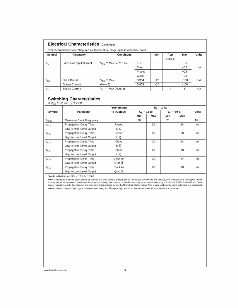
Electrical Characteristics (Continued)
over recommended operating free air temperature range (unless otherwise noted)
Symbol Parameter Conditions Min Typ Max Units
(Note 6)
IIL Low Level Input Current VCC = Max, VI = 0.4V J, K −0.4
Clear −0.8 mA
Preset −0.8
Clock −0.8
IOS Short Circuit VCC = Max DM54 −20 −100 mA
Output Current (Note 7) DM74 −20 −100
ICC Supply Current VCC = Max (Note 8) 4 6 mA
Switching Characteristicsat VCC = 5V and TA = 25˚C
From (Input) R L = 2 kΩSymbol Parameter To (Output) C L = 15 pF CL = 50 pF Units
Min Max Min Max
fMAX Maximum Clock Frequency 30 25 MHz
tPLH Propagation Delay Time Preset 20 24 ns
Low to High Level Output to Q
tPHL Propagation Delay Time Preset 20 28 ns
High to Low Level Output to Q
tPLH Propagation Delay Time Clear 20 24 ns
Low to High Level Output to Q
tPHL Propagation Delay Time Clear 20 28 ns
High to Low Level Output to Q
tPLH Propagation Delay Time Clock to 20 24 ns
Low to High Level Output Q or Q
tPHL Propagation Delay Time Clock to 20 28 ns
High to Low Level Output Q or Q
Note 6: All typicals are at VCC = 5V, TA = 25˚C.
Note 7: Not more than one output should be shorted at a time, and the duration should not exceed one second. For devices, with feedback from the outputs, whereshorting the outputs to ground may cause the outputs to change logic state an equivalent test may be performed where VO = 2.25V and 2.125V for DM54 and DM74series, respectively, with the minimum and maximum limits reduced by one half from their stated values. This is very useful when using automatic test equipment.
Note 8: With all outputs open, ICC is measured with the Q and Q outputs high in turn. At the time of measurement the clock is grounded.
www.fairchildsemi.com 4

5

Physical Dimensions inches (millimeters) unless otherwise noted
Ceramic Leadless Chip Carrier Package (E)Order Number 54LS112LMQB
Package Number E20A
16-Lead Ceramic Dual-In-Line Package (J)Order Number 54LS112DMQB or DM54LS112AJ
Package Number J16A
www.fairchildsemi.com 6

Physical Dimensions inches (millimeters) unless otherwise noted (Continued)
16-Lead Small Outline Molded Package (M)Order Number DM74LS112AM
Package Number M16A
16-Lead Molded Dual-In-Line Package (N)Order Number DM74LS112AN
Package Number N16E
7 www.fairchildsemi.com

Physical Dimensions inches (millimeters) unless otherwise noted (Continued)
LIFE SUPPORT POLICY
FAIRCHILD’S PRODUCTS ARE NOT AUTHORIZED FOR USE AS CRITICAL COMPONENTS IN LIFE SUPPORT DE-VICES OR SYSTEMS WITHOUT THE EXPRESS WRITTEN APPROVAL OF THE PRESIDENT OF FAIRCHILD SEMI-CONDUCTOR CORPORATION. As used herein:1. Life support devices or systems are devices or sys-
tems which, (a) are intended for surgical implant intothe body, or (b) support or sustain life, and (c) whosefailure to perform when properly used in accordancewith instructions for use provided in the labeling, canbe reasonably expected to result in a significant injuryto the user.
2. A critical component in any component of a life supportdevice or system whose failure to perform can be rea-sonably expected to cause the failure of the life supportdevice or system, or to affect its safety or effectiveness.
Fairchild SemiconductorCorporationAmericasCustomer Response CenterTel: 1-888-522-5372
www.fairchildsemi.com
Fairchild SemiconductorEurope
Fax: +49 (0) 1 80-530 85 86Email: [email protected]
Deutsch Tel: +49 (0) 8 141-35-0English Tel: +44 (0) 1 793-85-68-56Italy Tel: +39 (0) 2 57 5631
Fairchild SemiconductorHong Kong Ltd.13th Floor, Straight Block,Ocean Centre, 5 Canton Rd.Tsimshatsui, KowloonHong KongTel: +852 2737-7200Fax: +852 2314-0061
National SemiconductorJapan Ltd.Tel: 81-3-5620-6175Fax: 81-3-5620-6179
16-Lead Ceramic Flat Package (W)Order Number 54LS112FMQB or DM54LS112AW
Package Number W16A
DM
74LS
112A
Dua
lNeg
ativ
e-E
dge-
Trig
gere
dM
aste
r-S
lave
J-K
Flip
-Flo
psw
ithP
rese
t,C
lear
,and
Com
plem
enta
ryO
utpu
ts
Fairchild does not assume any responsibility for use of any circuitry described, no circuit patent licenses are implied and Fairchild reserves the right at any time without notice to change said circuitry and specifications.

DM74LS373/DM74LS3743-STATE Octal D-Type Transparent Latches andEdge-Triggered Flip-FlopsGeneral DescriptionThese 8-bit registers feature totem-pole 3-STATE outputsdesigned specifically for driving highly-capacitive or rela-tively low-impedance loads. The high-impedance state andincreased high-logic level drive provide these registers withthe capability of being connected directly to and driving thebus lines in a bus-organized system without need for inter-face or pull-up components. They are particularly attractivefor implementing buffer registers, I/O ports, bidirectional busdrivers, and working registers.
The eight latches of the DM54/74LS373 are transparentD-type latches meaning that while the enable (G) is high theQ outputs will follow the data (D) inputs. When the enable istaken low the output will be latched at the level of the datathat was set up.
The eight flip-flops of the DM54/74LS374 are edge-triggeredD-type flip flops. On the positive transition of the clock, the Qoutputs will be set to the logic states that were set up at theD inputs.
A buffered output control input can be used to place the eightoutputs in either a normal logic state (high or low logic levels)or a high-impedance state. In the high-impedance state theoutputs neither load nor drive the bus lines significantly.
The output control does not affect the internal operation ofthe latches or flip-flops. That is, the old data can be retainedor new data can be entered even while the outputs are off.
Featuresn Choice of 8 latches or 8 D-type flip-flops in a single
packagen 3-STATE bus-driving outputsn Full parallel-access for loadingn Buffered control inputsn P-N-P inputs reduce D-C loading on data lines
Connection Diagrams
Dual-In-Line Packages’LS373
DS006431-1
Order Number DM54LS373J, DM54LS373W, DM74LS373N or DM74LS373WMSee Package Number J20A, M20B, N20A or W20A
March 1998
DM
74LS373/D
M74LS
3743-S
TATEO
ctalD-Type
TransparentLatchesand
Edge-Triggered
Flip-Flops
© 1998 Fairchild Semiconductor Corporation DS006431 www.fairchildsemi.com

Connection Diagrams (Continued)
Function TablesDM54/74LS373
Output Enable D Output
Control G
L H H H
L H L L
L L X Q0
H X X Z
H = High Level (Steady State), L = Low Level (Steady State), X = Don’t Care↑ = Transition from low-to-high level, Z = High Impedance StateQ0 = The level of the output before steady-state input conditions were estab-lished.
DM54/74LS374Output Clock D Output
Control
L ↑ H H
L ↑ L L
L L X Q0
H X X Z
’LS374
DS006431-2
Order Number DM54LS374J, DM54LS374W, DM74LS374WM or DM74LS374NSee Package Number J20A, M20B, N20A or W20A
www.fairchildsemi.com 2
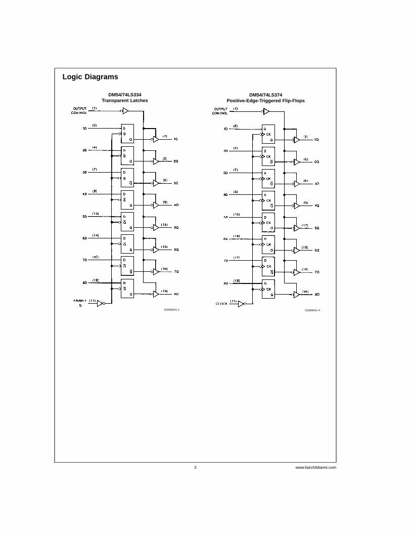
Logic Diagrams
DM54/74LS334Transparent Latches
DS006431-3
DM54/74LS374Positive-Edge-Triggered Flip-Flops
DS006431-4
3 www.fairchildsemi.com

Absolute Maximum Ratings (Note 1)
Supply Voltage 7VInput Voltage 7VStorage Temperature Range −65˚C to +150˚C
Operating Free Air Temperature RangeDM54LS −55˚C to +125˚CDM74LS 0˚C to +70˚C
Recommended Operating Conditions
Symbol Parameter DM54LS373 DM74LS373 Units
Min Nom Max Min Nom Max
VCC Supply Voltage 4.5 5 5.5 4.75 5 5.25 V
VIH High Level Input Votage 2 2 V
VIL Low Level Input Voltage 0.7 0.8 V
IOH High Level Output Current −1 −2.6 mA
IOL Low Level Output Current 12 24 mA
tW Pulse Width Enable High 15 15 ns
(Note 3) Enable Low 15 15
tSU Data Setup Time (Notes 2, 3) 5↓ 5↓ ns
tH Data Hold Time (Notes 2, 3) 20↓ 20↓ ns
TA Free Air Operating Temperature −55 125 0 70 ˚CNote 1: The “Absolute Maximum Ratings” are those values beyond which the safety of the device cannot be guaranteed. The device should not be operated at theselimits. The parametric values defined in the “Electrical Characteristics” table are not guaranteed at the absolute maximum ratings. The “Recommended OperatingConditions” table will define the conditions for actual device operation.
Note 2: The symbol (↓) indicates the falling edge of the clock pulse is used for reference.
Note 3: TA = 25˚C and VCC = 5V.
’LS373 Electrical Characteristicsover recommended operating free air temperature range (unless otherwise noted)
Symbol Parameter Conditions Min Typ Max Units
(Note 4)
VI Input Clamp Voltage VCC = Min, II = −18 mA −1.5 V
VOH High Level Output Voltage VCC = Min DM54 2.4 3.4
IOH = Max V
VIL = Max DM74 2.4 3.1
VIH = Min
VOL Low Level Output Voltage VCC = Min DM54 0.25 0.4
IOL = Max
VIL = Max DM74 0.35 0.5 V
VIH = Min
IOL = 12 mA DM74 0.4
VCC = Min
II Input Current @ Max VCC = Max, VI = 7V 0.1 mA
Input Voltage
IIH High Level Input Current VCC = Max, VI = 2.7V 20 µA
IIL Low Level Input Current VCC = Max, VI = 0.4V −0.4 mA
IOZH Off-State Output Current VCC = Max, VO = 2.7V
with High Level Output VIH = Min, VIL = Max 20 µA
Voltage Applied
IOZL Off-State Output Current VCC = Max, VO = 0.4V
with Low Level Output VIH = Min, VIL = Max −20 µA
Voltage Applied
IOS Short Circuit VCC = Max DM54 −20 −100 mA
Output Current (Note 5) DM74 −50 −225
www.fairchildsemi.com 4

’LS373 Electrical Characteristics (Continued)
over recommended operating free air temperature range (unless otherwise noted)
Symbol Parameter Conditions Min Typ Max Units
(Note 4)
ICC Supply Current VCC = Max, OC = 4.5V, 24 40 mA
Dn, Enable = GND
’LS373 Switching Characteristicsat VCC = 5V and TA = 25˚C
From R L = 667ΩSymbol Parameter (Input) C L = 45 pF CL = 150 pF Units
To Min Max Min Max
(Output)
tPLH Propagation Delay Data
Time Low to High to 18 26 ns
Level Output Q
tPHL Propagation Delay Data
Time High to Low to 18 27 ns
Level Output Q
tPLH Propagation Delay Enable
Time Low to High to 30 38 ns
Level Output Q
tPHL Propagation Delay Enable
Time High to Low to 30 36 ns
Level Output Q
tPZH Output Enable Output
Time to High Control 28 36 ns
Level Output to Any Q
tPZL Output Enable Output
Time to Low Control 36 50 ns
Level Output to Any Q
tPHZ Output Disable Output
Time from High Control 20 ns
Level Output (Note 6) to Any Q
tPLZ Output Disable Output
Time from Low Control 25 ns
Level Output (Note 6) to Any Q
Note 4: All typicals are at VCC = 5V, TA = 25˚C.
Note 5: Not more than one output should be shorted at a time, and the duration should not exceed one second.
Note 6: CL = 5 pF.
Recommended Operating Conditions
Symbol Parameter DM54LS374 DM74LS374 Units
Min Nom Max Min Nom Max
VCC Supply Voltage 4.5 5 5.5 4.75 5 5.25 V
VIH High Level Input Voltage 2 2 V
VIL Low Level Input Voltage 0.7 0.8 V
IOH High Level Output Current −1 −2.6 mA
IOL Low Level Output Current 12 24 mA
5 www.fairchildsemi.com

Recommended Operating Conditions (Continued)
Symbol Parameter DM54LS374 DM74LS374 Units
Min Nom Max Min Nom Max
tW Pulse Width Clock High 15 15 ns
(Note 8) Clock Low 15 15
tSU Data Setup Time (Notes 7, 8) 20↑ 20↑ ns
tH Data Hold Time (Notes 7, 8) 1↑ 1↑ ns
TA Free Air Operating Temperature −55 125 0 70 ˚C
Note 7: The symbol (↑) indicates the rising edge of the clock pulse is used for reference.
Note 8: TA = 25˚C and VCC = 5V.
’LS374 Electrical Characteristicsover recommended operating free air temperature range (unless otherwise noted)
Symbol Parameter Conditions Min Typ Max Units
(Note 9)
VI Input Clamp Voltage VCC = Min, II = −18 mA −1.5 V
VOH High Level Output Voltage VCC = Min DM54 2.4 3.4
IOH = Max DM74 2.4 3.1 V
VIL = Max
VIH = Min
VOL Low Level Output Voltage VCC = Min DM54 0.25 0.4
IOL = Max DM74 0.35 0.5
VIL = Max V
VIH = Min
IOL = 12 mA DM74 0.25 0.4
VCC = Min
II Input Current @ Max VCC = Max, VI = 7V 0.1 mA
Input Voltage
IIH High Level Input Current VCC = Max, VI = 2.7V 20 µA
IIL Low Level Input Current VCC = Max, VI = 0.4V −0.4 mA
IOZH Off-State Output VCC = Max, VO = 2.7V
Current with High VIH = Min, VIL = Max 20 µA
Level Output
Voltage Applied
IOZL Off-State Output VCC = Max, VO = 0.4V
Current with Low VIH = Min, VIL = Max −20 µA
Level Output
Voltage Applied
IOS Short Circuit VCC = Max DM54 −50 −225 mA
Output Current (Note 10) DM74 −50 −225
ICC Supply Current VCC = Max, Dn =GND, OC = 4.5V
27 45 mA
www.fairchildsemi.com 6

’LS374 Switching Characteristicsat VCC = 5V and TA = 25˚C
RL = 667ΩSymbol Parameter C L = 45 pF CL = 150 pF Units
Min Max Min Max
fMAX Maximum Clock Frequency 35 20 MHz
tPLH Propagation Delay Time 28 32 ns
Low to High Level Output
tPHL Propagation Delay Time 28 38 ns
High to Low Level Output
tPZH Output Enable Time 28 44 ns
to High Level Output
tPZL Output Enable Time 28 44 ns
to Low Level Output
tPHZ Output Disable Time 20 ns
from High Level Output (Note 11)
tPLZ Output Disable Time 25 ns
from Low Level Output (Note 11)
Note 9: All typicals are at VCC = 5V, TA = 25˚C.
Note 10: Not more than one output should be shorted at a time, and the duration should not exceed one second.
Note 11: CL = 5 pF.
7 www.fairchildsemi.com

Physical Dimensions inches (millimeters) unless otherwise noted
20-Lead Ceramic Dual-In-Line Package (J)Order Number DM54LS373J or DM54LS374J
Package Number J20A
20-Lead Wide Small Outline Molded Package (M)Order Number DM74LS373WM or DM74LS374WM
Package Number M20B
www.fairchildsemi.com 8

Physical Dimensions inches (millimeters) unless otherwise noted (Continued)
20-Lead Molded Dual-In-Line Package (N)Order Number DM74LS373N and DM74LS374N
Package Number N20A
20-Lead Ceramic Flat Package (W)Order Number DM54LS373W or DM54LS374W
Package Number W20A
9 www.fairchildsemi.com

LIFE SUPPORT POLICY
FAIRCHILD’S PRODUCTS ARE NOT AUTHORIZED FOR USE AS CRITICAL COMPONENTS IN LIFE SUPPORT DE-VICES OR SYSTEMS WITHOUT THE EXPRESS WRITTEN APPROVAL OF THE PRESIDENT OF FAIRCHILD SEMI-CONDUCTOR CORPORATION. As used herein:1. Life support devices or systems are devices or sys-
tems which, (a) are intended for surgical implant intothe body, or (b) support or sustain life, and (c) whosefailure to perform when properly used in accordancewith instructions for use provided in the labeling, canbe reasonably expected to result in a significant injuryto the user.
2. A critical component in any component of a life supportdevice or system whose failure to perform can be rea-sonably expected to cause the failure of the life supportdevice or system, or to affect its safety or effectiveness.
Fairchild SemiconductorCorporationAmericasCustomer Response CenterTel: 1-888-522-5372
www.fairchildsemi.com
Fairchild SemiconductorEurope
Fax: +49 (0) 1 80-530 85 86Email: [email protected]
Deutsch Tel: +49 (0) 8 141-35-0English Tel: +44 (0) 1 793-85-68-56Italy Tel: +39 (0) 2 57 5631
Fairchild SemiconductorHong Kong Ltd.13th Floor, Straight Block,Ocean Centre, 5 Canton Rd.Tsimshatsui, KowloonHong KongTel: +852 2737-7200Fax: +852 2314-0061
National SemiconductorJapan Ltd.Tel: 81-3-5620-6175Fax: 81-3-5620-6179
DM
74LS
373/
DM
74LS
374
3-S
TATE
Oct
alD
-Typ
eTr
ansp
aren
tLat
ches
and
Edg
e-Tr
igge
red
Flip
-Flo
ps
Fairchild does not assume any responsibility for use of any circuitry described, no circuit patent licenses are implied and Fairchild reserves the right at any time without notice to change said circuitry and specifications.

LM555/LM555CTimerGeneral DescriptionThe LM555 is a highly stable device for generating accuratetime delays or oscillation. Additional terminals are providedfor triggering or resetting if desired. In the time delay mode ofoperation, the time is precisely controlled by one external re-sistor and capacitor. For astable operation as an oscillator,the free running frequency and duty cycle are accuratelycontrolled with two external resistors and one capacitor. Thecircuit may be triggered and reset on falling waveforms, andthe output circuit can source or sink up to 200 mA or driveTTL circuits.
Featuresn Direct replacement for SE555/NE555n Timing from microseconds through hoursn Operates in both astable and monostable modesn Adjustable duty cyclen Output can source or sink 200 mAn Output and supply TTL compatiblen Temperature stability better than 0.005% per ˚Cn Normally on and normally off outputn Available in 8 pin MSOP package
Applicationsn Precision timingn Pulse generationn Sequential timingn Time delay generationn Pulse width modulationn Pulse position modulationn Linear ramp generator
Schematic Diagram
DS007851-1
May 1997
LM555/LM
555CTim
er
© 1997 National Semiconductor Corporation DS007851 www.national.com

Absolute Maximum Ratings (Note 2)
If Military/Aerospace specified devices are required,please contact the National Semiconductor Sales Office/Distributors for availability and specifications.
Supply Voltage +18VPower Dissipation (Note 3)LM555H, LM555CH 760 mWLM555, LM555CN 1180 mWLM555CMM 613 mW
Operating Temperature RangesLM555C 0˚C to +70˚CLM555 −55˚C to + 125˚C
Storage Temperature Range −65˚C to +150˚CSoldering InformationDual-In-Line PackageSoldering (10 Seconds) 260˚C
Small Outline Packages(SOIC and MSOP)Vapor Phase (60 Seconds) 215˚CInfrared (15 Seconds) 220˚C
See AN-450 “Surface Mounting Methods and Their Effecton Product Reliability” for other methods of solderingsurface mount devices.
Electrical Characteristics (Notes 1, 2)
(TA = 25˚C, VCC = +5V to +15V, unless othewise specified)
Limits
Parameter Conditions LM555 LM555C Units
Min Typ Max Min Typ Max
Supply Voltage 4.5 18 4.5 16 V
Supply Current VCC = 5V, RL = ∞ 3 5 3 6 mA
VCC = 15V, RL = ∞ 10 12 10 15 mA
(Low State) (Note 4)
Timing Error, Monostable
Initial Accuracy 0.5 1 %
Drift with Temperature RA = 1k to 100 kΩ, 30 50 ppm/˚C
C = 0.1 µF, (Note 5)
Accuracy over Temperature 1.5 1.5 %
Drift with Supply 0.05 0.1 %/V
Timing Error, Astable
Initial Accuracy 1.5 2.25 %
Drift with Temperature RA, RB = 1k to 100 kΩ, 90 150 ppm/˚C
C = 0.1 µF, (Note 5)
Accuracy over Temperature 2.5 3.0 %
Drift with Supply 0.15 0.30 %/V
Threshold Voltage 0.667 0.667 x VCCTrigger Voltage VCC = 15V 4.8 5 5.2 5 V
VCC = 5V 1.45 1.67 1.9 1.67 V
Trigger Current 0.01 0.5 0.5 0.9 µA
Reset Voltage 0.4 0.5 1 0.4 0.5 1 V
Reset Current 0.1 0.4 0.1 0.4 mA
Threshold Current (Note 6) 0.1 0.25 0.1 0.25 µA
Control Voltage Level VCC = 15V 9.6 10 10.4 9 10 11 V
VCC = 5V 2.9 3.33 3.8 2.6 3.33 4 V
Pin 7 Leakage Output High 1 100 1 100 nA
Pin 7 Sat (Note 7)
Output Low VCC = 15V, I7 = 15 mA 150 180 mV
Output Low VCC = 4.5V, I7 = 4.5 mA 70 100 80 200 mV
www.national.com 2

Electrical Characteristics (Notes 1, 2) (Continued)
(TA = 25˚C, VCC = +5V to +15V, unless othewise specified)
Limits
Parameter Conditions LM555 LM555C Units
Min Typ Max Min Typ Max
Output Voltage Drop (Low) VCC = 15V
ISINK = 10 mA 0.1 0.15 0.1 0.25 V
ISINK = 50 mA 0.4 0.5 0.4 0.75 V
ISINK = 100 mA 2 2.2 2 2.5 V
ISINK = 200 mA 2.5 2.5 V
VCC = 5V
ISINK = 8 mA 0.1 0.25 V
ISINK = 5 mA 0.25 0.35 V
Output Voltage Drop (High) ISOURCE = 200 mA, VCC = 15V 12.5 12.5 V
ISOURCE = 100 mA, VCC = 15V 13 13.3 12.75 13.3 V
VCC = 5V 3 3.3 2.75 3.3 V
Rise Time of Output 100 100 ns
Fall Time of Output 100 100 ns
Note 1: All voltages are measured with respect to the ground pin, unless otherwise specified.
Note 2: Absolute Maximum Ratings indicate limits beyond which damage to the device may occur. Operating Ratings indicate conditions for which the device is func-tional, but do not guarantee specific performance limits. Electrical Characteristics state DC andAC electrical specifications under particular test conditions which guar-antee specific performance limits. This assumes that the device is within the Operating Ratings. Specifications are not guaranteed for parameters where no limit isgiven, however, the typical value is a good indication of device performance.
Note 3: For operating at elevated temperatures the device must be derated above 25˚C based on a +150˚C maximum junction temperature and a thermal resistanceof 164˚C/W (T0-5), 106˚C/W (DIP), 170˚C/W (S0-8), and 204˚C/W (MSOP) junction to ambient.
Note 4: Supply current when output high typically 1 mA less at VCC = 5V.
Note 5: Tested at VCC = 5V and VCC = 15V.
Note 6: This will determine the maximum value of RA + RB for 15V operation. The maximum total (RA + RB) is 20 MΩ.
Note 7: No protection against excessive pin 7 current is necessary providing the package dissipation rating will not be exceeded.
Note 8: Refer to RETS555X drawing of military LM555H and LM555J versions for specifications.
Connection Diagrams
Metal Can Package
DS007851-2
Top ViewOrder Number LM555H or LM555CHSee NS Package Number H08C
Dual-In-Line, Small Outlineand Molded Mini Small Outline Packages
DS007851-3
Top ViewOrder Number LM555J, LM555CJ,LM555CM, LM555CMM or LM555CN
See NS Package Number J08A, M08A, MUA08A orN08E
3 www.national.com
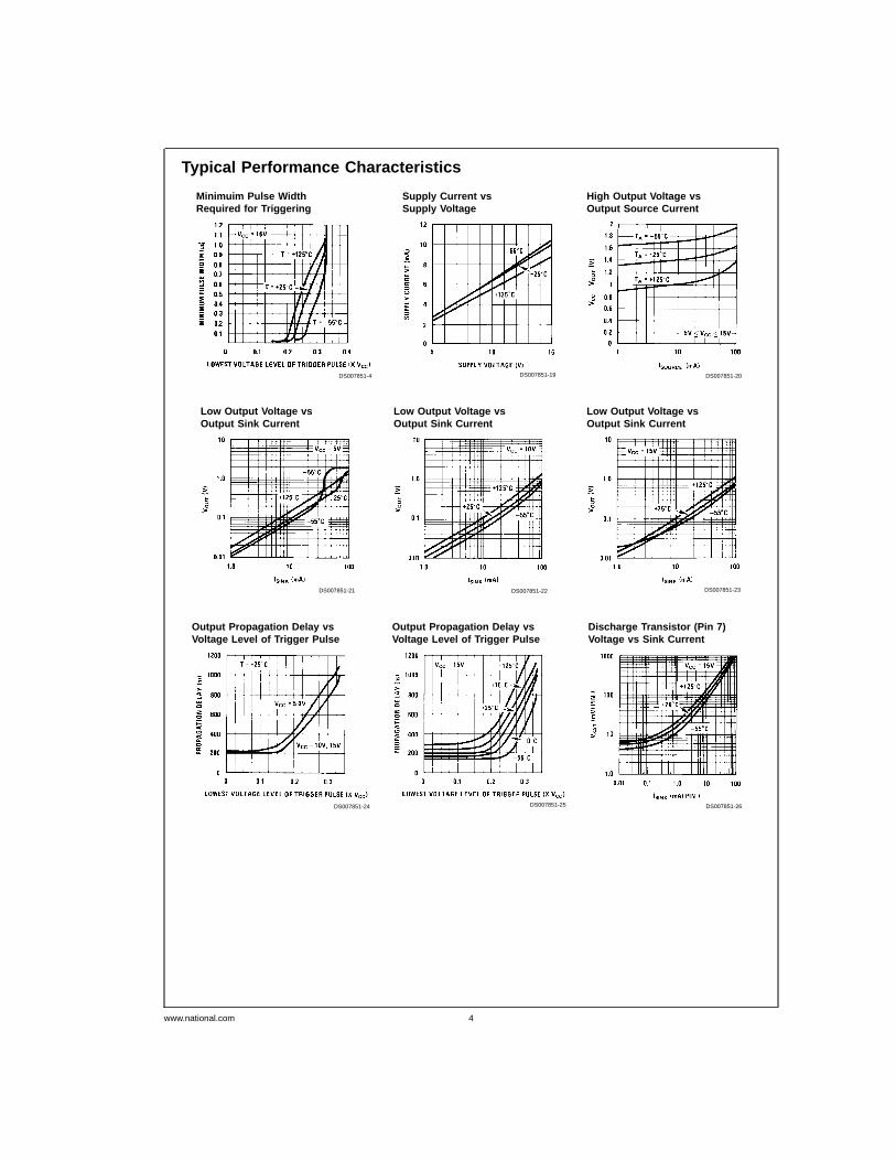
Typical Performance Characteristics
Minimuim Pulse WidthRequired for Triggering
DS007851-4
Supply Current vsSupply Voltage
DS007851-19
High Output Voltage vsOutput Source Current
DS007851-20
Low Output Voltage vsOutput Sink Current
DS007851-21
Low Output Voltage vsOutput Sink Current
DS007851-22
Low Output Voltage vsOutput Sink Current
DS007851-23
Output Propagation Delay vsVoltage Level of Trigger Pulse
DS007851-24
Output Propagation Delay vsVoltage Level of Trigger Pulse
DS007851-25
Discharge Transistor (Pin 7)Voltage vs Sink Current
DS007851-26
www.national.com 4

Typical Performance Characteristics (Continued)
Applications InformationMONOSTABLE OPERATION
In this mode of operation, the timer functions as a one-shot(Figure 1). The external capacitor is initially held dischargedby a transistor inside the timer. Upon application of a nega-tive trigger pulse of less than 1/3 VCC to pin 2, the flip-flop isset which both releases the short circuit across the capacitorand drives the output high.
The voltage across the capacitor then increases exponen-tially for a period of t = 1.1 RA C, at the end of which time thevoltage equals 2/3 VCC. The comparator then resets theflip-flop which in turn discharges the capacitor and drives theoutput to its low state. Figure 2 shows the waveforms gener-ated in this mode of operation. Since the charge and thethreshold level of the comparator are both directly propor-tional to supply voltage, the timing internal is independent ofsupply.
During the timing cycle when the output is high, the furtherapplication of a trigger pulse will not effect the circuit so longas the trigger input is returned high at least 10 µs before theend of the timing interval. However the circuit can be resetduring this time by the application of a negative pulse to thereset terminal (pin 4). The output will then remain in the lowstate until a trigger pulse is again applied.
When the reset function is not in use, it is recommended thatit be connected to VCC to avoid any possibility of false trig-gering.
Figure 3 is a nomograph for easy determination of R, C val-ues for various time delays.
NOTE: In monostable operation, the trigger should be drivenhigh before the end of timing cycle.
Discharge Transistor (Pin 7)Voltage vs Sink Current
DS007851-27
DS007851-5
FIGURE 1. Monostable
DS007851-6
VCC = 5V Top Trace: Input 5V/Div.TIME = 0.1 ms/DIV. Middle Trace: Output 5V/Div.RA = 9.1 kΩ Bottom Trace: Capacitor Voltage 2V/Div.C = 0.01 µF
FIGURE 2. Monostable Waveforms
5 www.national.com

Applications Information (Continued)
ASTABLE OPERATION
If the circuit is connected as shown in Figure 4 (pins 2 and 6connected) it will trigger itself and free run as a multivibrator.The external capacitor charges through RA + RB and dis-charges through RB. Thus the duty cycle may be preciselyset by the ratio of these two resistors.
In this mode of operation, the capacitor charges and dis-charges between 1/3 VCC and 2/3 VCC. As in the triggeredmode, the charge and discharge times, and therefore the fre-quency are independent of the supply voltage.
Figure 5 shows the waveforms generated in this mode ofoperation.
The charge time (output high) is given by:
t1 = 0.693 (RA + RB) C
And the discharge time (output low) by:
t2 = 0.693 (RB) C
Thus the total period is:
T = t1 + t2 = 0.693 (RA +2RB) C
The frequency of oscillation is:
Figure 6 may be used for quick determination of these RCvalues.
The duty cycle is:
FREQUENCY DIVIDER
The monostable circuit of Figure 1 can be used as a fre-quency divider by adjusting the length of the timing cycle.Figure 7 shows the waveforms generated in a divide by threecircuit.
DS007851-7
FIGURE 3. Time Delay
DS007851-8
FIGURE 4. Astable
DS007851-9
VCC = 5V Top Trace: Output 5V/Div.TIME = 20 µs/DIV. Bottom Trace: Capacitor Voltage 1V/Div.RA = 3.9 kΩRB = 3 kΩC = 0.01 µF
FIGURE 5. Astable Waveforms
DS007851-10
FIGURE 6. Free Running Frequency
www.national.com 6
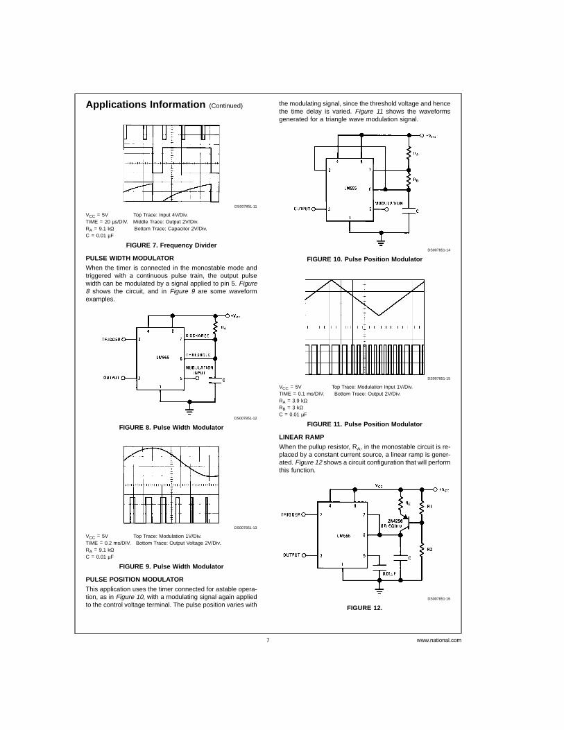
Applications Information (Continued)
PULSE WIDTH MODULATOR
When the timer is connected in the monostable mode andtriggered with a continuous pulse train, the output pulsewidth can be modulated by a signal applied to pin 5. Figure8 shows the circuit, and in Figure 9 are some waveformexamples.
PULSE POSITION MODULATOR
This application uses the timer connected for astable opera-tion, as in Figure 10, with a modulating signal again appliedto the control voltage terminal. The pulse position varies with
the modulating signal, since the threshold voltage and hencethe time delay is varied. Figure 11 shows the waveformsgenerated for a triangle wave modulation signal.
LINEAR RAMP
When the pullup resistor, RA, in the monostable circuit is re-placed by a constant current source, a linear ramp is gener-ated. Figure 12 shows a circuit configuration that will performthis function.
DS007851-11
VCC = 5V Top Trace: Input 4V/Div.TIME = 20 µs/DIV. Middle Trace: Output 2V/Div.RA = 9.1 kΩ Bottom Trace: Capacitor 2V/Div.C = 0.01 µF
FIGURE 7. Frequency Divider
DS007851-12
FIGURE 8. Pulse Width Modulator
DS007851-13
VCC = 5V Top Trace: Modulation 1V/Div.TIME = 0.2 ms/DIV. Bottom Trace: Output Voltage 2V/Div.RA = 9.1 kΩC = 0.01 µF
FIGURE 9. Pulse Width Modulator
DS007851-14
FIGURE 10. Pulse Position Modulator
DS007851-15
VCC = 5V Top Trace: Modulation Input 1V/Div.TIME = 0.1 ms/DIV. Bottom Trace: Output 2V/Div.RA = 3.9 kΩRB = 3 kΩC = 0.01 µF
FIGURE 11. Pulse Position Modulator
DS007851-16
FIGURE 12.
7 www.national.com

Applications Information (Continued)
Figure 13 shows waveforms generated by the linear ramp.
The time interval is given by:
VBE ≅ 0.6V
50% DUTY CYCLE OSCILLATOR
For a 50% duty cycle, the resistors RA and RB may be con-nected as in Figure 14. The time period for the output high isthe same as previous, t1 = 0.693 RA C. For the output low itis t2 =
Thus the frequency of oscillation is
Note that this circuit will not oscillate if RB is greater than 1/2RA because the junction of RA and RB cannot bring pin 2down to 1/3 VCC and trigger the lower comparator.
ADDITIONAL INFORMATION
Adequate power supply bypassing is necessary to protectassociated circuitry. Minimum recommended is 0.1 µF in par-allel with 1 µF electrolytic.
Lower comparator storage time can be as long as 10 µswhen pin 2 is driven fully to ground for triggering. This limitsthe monostable pulse width to 10 µs minimum.
Delay time reset to output is 0.47 µs typical. Minimum resetpulse width must be 0.3 µs, typical.
Pin 7 current switches within 30 ns of the output (pin 3) volt-age.
DS007851-17
VCC = 5V Top Trace: Input 3V/Div.TIME = 20 µs/DIV. Middle Trace: Output 5V/Div.R1 = 47 kΩ Bottom Trace: Capacitor Voltage 1V/Div.R2 = 100 kΩRE = 2.7 kΩC = 0.01 µF
FIGURE 13. Linear Ramp
DS007851-18
FIGURE 14. 50% Duty Cycle Oscillator
www.national.com 8

Physical Dimensions inches (millimeters)
Metal Can Package (H)Order Number LM555H or LM555CH
NS Package Number H08C
Ceramic Dual-In-Line Package (J)Order Number LM555J or LM555CJ
NS Package Number J08A
9 www.national.com
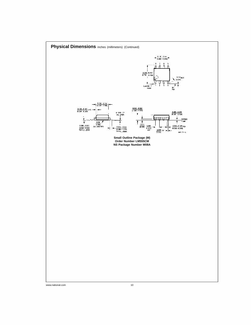
Physical Dimensions inches (millimeters) (Continued)
Small Outline Package (M)Order Number LM555CMNS Package Number M08A
www.national.com 10

Physical Dimensions inches (millimeters) (Continued)
8-Lead (0.118” Wide) Molded Mini Small Outline PackageOrder Number LM555CMM
NS Package Number MUA08A
11 www.national.com

Physical Dimensions inches (millimeters) (Continued)
LIFE SUPPORT POLICY
NATIONAL’S PRODUCTS ARE NOT AUTHORIZED FOR USE AS CRITICAL COMPONENTS IN LIFE SUPPORT DE-VICES OR SYSTEMS WITHOUT THE EXPRESS WRITTEN APPROVAL OF THE PRESIDENT OF NATIONAL SEMI-CONDUCTOR CORPORATION. As used herein:1. Life support devices or systems are devices or sys-
tems which, (a) are intended for surgical implant intothe body, or (b) support or sustain life, and whose fail-ure to perform when properly used in accordancewith instructions for use provided in the labeling, canbe reasonably expected to result in a significant injuryto the user.
2. A critical component in any component of a life supportdevice or system whose failure to perform can be rea-sonably expected to cause the failure of the life supportdevice or system, or to affect its safety or effectiveness.
National SemiconductorCorporation1111 West Bardin RoadArlington, TX 76017Tel: 1(800) 272-9959Fax: 1(800) 737-7018
www.national.com
National SemiconductorEurope
Fax: (+49) 0-180-530 85 86Email: [email protected]
Deutsch Tel: (+49) 0-180-530 85 85English Tel: (+49) 0-180-532 78 32Français Tel: (+49) 0-180-532 93 58Italiano Tel: (+49) 0-180-534 16 80
National SemiconductorHong Kong Ltd.13th Floor, Straight Block,Ocean Centre, 5 Canton Rd.Tsimshatsui, KowloonHong KongTel: (852) 2737-1600Fax: (852) 2736-9960
National SemiconductorJapan Ltd.Tel: 81-043-299-2308Fax: 81-043-299-2408
Molded Dual-In-Line Package (N)Order Number LM555CNNS Package Number N08E
LM555/LM
555C
Timer
National does not assume any responsibility for use of any circuitry described, no circuit patent licenses are implied and National reserves the right at any time without notice to change said circuitry and specifications.