pxie-5624 specifications - national instruments · the labview instrument design libraries for if...
TRANSCRIPT

SPECIFICATIONS
PXIe-5624IF Digitizer
ContentsDefinitions.................................................................................................................................2Conditions................................................................................................................................. 2Modes of Operation.................................................................................................................. 2Frequency..................................................................................................................................3
Internal Frequency Reference........................................................................................... 3Frequency Reference/ADC Sample Clock Input (CLK IN)............................................. 4Frequency Reference/ADC Sample Clock Output (CLK OUT)...................................... 4Spectral Purity...................................................................................................................4
IF Input (IF IN)......................................................................................................................... 6Absolute Amplitude Accuracy..........................................................................................7Frequency Response......................................................................................................... 8Average Noise Density......................................................................................................8
Spurious Responses.................................................................................................................10Digitizer Mode................................................................................................................ 10DDC Mode...................................................................................................................... 11
Error Vector Magnitude (EVM)..............................................................................................14Digitizer Characteristics..........................................................................................................14
Onboard FPGA............................................................................................................... 14Onboard DRAM..............................................................................................................14Onboard SRAM.............................................................................................................. 14
Front Panel I/O........................................................................................................................15IF IN................................................................................................................................15CLK IN........................................................................................................................... 15CLK OUT....................................................................................................................... 15PFI 0 (Programmable Function Interface)...................................................................... 16AUX I/O..........................................................................................................................16
Power Requirements............................................................................................................... 18Calibration...............................................................................................................................18Physical Characteristics.......................................................................................................... 18Environment............................................................................................................................18
Operating Environment...................................................................................................19Storage Environment.......................................................................................................19

Shock and Vibration................................................................................................................19Compliance and Certifications................................................................................................19
Safety.............................................................................................................................. 19Electromagnetic Compatibility....................................................................................... 20CE Compliance .............................................................................................................. 20Online Product Certification........................................................................................... 20Environmental Management........................................................................................... 20
DefinitionsWarranted specifications describe the performance of a model under stated operatingconditions and are covered by the model warranty.
The following characteristic specifications describe values that are relevant to the use of themodel under stated operating conditions but are not covered by the model warranty.• Typical specifications describe the performance met by a majority of models.• Nominal specifications describe an attribute that is based on design, conformance testing,
or supplemental testing.
Specifications are Warranted unless otherwise noted.
ConditionsSpecifications are valid under the following conditions unless otherwise noted.• Internal Reference Clock source is used.• Dither level is set to high.• Digital downconversion (DDC) mode enabled.
Warranted specifications are valid under the following conditions unless otherwise noted.• 20 minutes warm-up time after the chassis is powered on and the LabVIEW Instrument
Design Libraries for IF Digitizers software is loaded and recognizes the PXIe-5624. Thewarm-up time ensures that the PXIe-5624 and test instrumentation are at a stableoperating temperature.
• Calibration cycle is maintained.• Calibration IP is used properly during the creation of custom FPGA bitfiles.1
• Chassis fan speed is set to high. In addition, NI recommends using slot blockers andEMC filler panels in empty module slots to minimize temperature drift.
Modes of OperationThe PXIe-5624 is a software designed instrument with a user-programmable FPGA.
1 Refer to the NI IF Digitizers Help for more information about calibration IP.
2 | ni.com | PXIe-5624 Specifications

The LabVIEW Instrument Design Libraries for IF Digitizers includes example FPGA imagesto use the PXIe-5624 in two modes of operation.
Digitizer Mode Data from the ADC is stored directly into DRAM on thePXIe-5624 and fetched from the host. This data is not equalized orcalibrated.
DigitalDownconversion(DDC) Mode
Data from the ADC goes through signal processing before beingstored in DRAM. The data is shifted in frequency, decimated,equalized, and calibrated using digital signal processing (DSP) onthe FPGA.
FrequencyInput frequency range (3 dB bandwidth) 5 MHz to 2 GHz, typical2
Equalized bandwidth
400 MHz acquisition FPGA image3 95 Hz to 400 MHz
800 MHz acquisition FPGA image3 800 MHz
Note The equalized bandwidth cannot cross Nyquist boundaries:5 MHz ≤ DDC Center Frequency ± BW/2 ≤ 1 GHz,1 GHz ≤ DDC Center Frequency ± BW/2 ≤ 2 GHz
Bandwidth resolution (400 MHzacquisition FPGA image3)
3.56 μHz
Frequency shift resolution 7.13 μHz
Dither frequency range 1 MHz to 50 MHz, typical
Internal Frequency ReferenceInitial adjustment accuracy ±0.2 × 10⁻⁶
Temperature stability
23 ± 5 °C ±0.5 × 10⁻⁶, nominal
0 °C to 55 °C ±2.0 × 10⁻⁶, maximum
Aging ±0.5 × 10⁻⁶ per year, maximum
Accuracy Initial adjustment accuracy ± Aging ±Temperature stability
2 Refer to Frequency Response for more information about this specification.3 Refer to the NI PXIe-5624R Getting Started Guide for more information about FPGA images.
PXIe-5624 Specifications | © National Instruments | 3

Frequency Reference/ADC Sample Clock Input(CLK IN)Refer to CLK IN for more information about frequency reference/ADC Sample Clock input(CLK IN).
Frequency Reference/ADC Sample Clock Output(CLK OUT)Refer to CLK OUT for more information about frequency reference/ADC Sample Clockoutput (CLK OUT).
Spectral PuritySampling jitter, nominal
CLK OUT 172 fs RMS4
IF IN 172 fs RMS5
Table 1. Single Sideband Phase Noise6
Carrier Frequency (MHz) Offset SSB Phase Noise (dBc/Hz), Typical
187.5 100 Hz -95
1 kHz -115
10 kHz -133
100 kHz -147
1 MHz -149
800 100 Hz -82
1 kHz -103
10 kHz -119
100 kHz -142
1 MHz -146
4 Conditions: 2 GHz ADC Sample Clock integrated from 100 Hz to 10 MHz. Refer to the MeasuredSampling Clock Phase Noise with an Internal Reference Clock, 2 GHz figure.
5 Conditions: 800 MHz input, locked to internal Reference Clock, integrated from 100 Hz to10 MHz. Refer to the Measured SSB Phase Noise of Internal Reference, Multiple Frequenciesfigure.
6 Conditions: Dither disabled, single-tone input level of 7 dBm.
4 | ni.com | PXIe-5624 Specifications

Figure 1. Measured SSB Phase Noise7 at 187 MHz, Multiple Clock Configurations8
10 –160
–150
–140
–130
–120
–110
–100
–90
–80
–70
–60
–50
100 1k 10kOffset Frequency (Hz)
SS
B P
hase
Noi
se (
dBc/
Hz)
100k 1M 10M
Internal ReferenceExternal 100 MHz OCXO Reference
PXI Express Backplane 100 MHz Reference
Figure 2. Measured SSB Phase Noise9 of Internal Reference, Multiple CarrierFrequencies10
10 –160
–150
–140
–130
–120
–110
–100
–90
–80
–70
–60
–50
100 1k 10kOffset Frequency (Hz)
SS
B P
hase
Noi
se (
dBc/
Hz)
100k 1M 10M
800 MHz Carrier Frequency187 MHz Carrier Frequency
7 Conditions: Dither disabled, single tone input level of 7 dBm. CW spurs removed from plots.OCXO source is PXIe-5653. Backplane PXI Express 100 MHz source is an PXIe-1085 chassis.
8 Phase noise measurement at 187 MHz limited from 100 kHz to 1 MHz by signal generator.9 Conditions: Dither disabled, single-tone input level of 7 dBm.
10 Phase noise measurement at 187 MHz limited from 100 kHz to 1 MHz by signal generator.
PXIe-5624 Specifications | © National Instruments | 5

Figure 3. Measured Sampling Clock Phase Noise11 with an Internal Reference Clock,2 GHz
10 –160
–150
–140
–130
–120
–110
–100
–90
–80
–70
–60
–40
–50
100 1k 10kOffset Frequency (Hz)
SS
B P
hase
Noi
se (
dBc/
Hz)
100k 1M 10M
IF Input (IF IN)Number of channels 1 (IF IN)
Table 2. Full-Scale Input Range
Dither Setting Value Value (dBm), Typical
Off 8 dBm (1.58 Vpk-pk) 9
On 6 dBm (1.26 Vpk-pk) 7
11 Conditions: Measured on unit configured to export ADC Sample Clock from REF OUT whenusing an internal Reference Clock. CW spurs removed.
6 | ni.com | PXIe-5624 Specifications
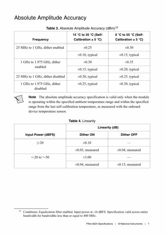
Absolute Amplitude Accuracy
Table 3. Absolute Amplitude Accuracy (dBm)12
Frequency15 °C to 35 °C (Self-Calibration ± 5 °C)
0 °C to 55 °C (Self-Calibration ± 5 °C)
25 MHz to 1 GHz, dither enabled ±0.25 ±0.30
±0.10, typical ±0.15, typical
1 GHz to 1.975 GHz, ditherenabled
±0.30 ±0.35
±0.15, typical ±0.20, typical
25 MHz to 1 GHz, dither disabled ±0.20, typical ±0.25, typical
1 GHz to 1.975 GHz, ditherdisabled
±0.25, typical ±0.30, typical
Note The absolute amplitude accuracy specification is valid only when the moduleis operating within the specified ambient temperature range and within the specifiedrange from the last self-calibration temperature, as measured with the onboarddevice temperature sensor.
Table 4. Linearity
Input Power (dBFS)
Linearity (dB)
Dither ON Dither OFF
≥-20 ±0.10 —
±0.03, measured ±0.04, measured
<-20 to >-50 ±3.00 —
±0.04, measured ±0.15, measured
12 Conditions: Equalization filter enabled. Input power at -16 dBFS. Specification valid across entirebandwidth for bandwidths less than or equal to 400 MHz.
PXIe-5624 Specifications | © National Instruments | 7

Frequency ResponseFigure 4. Measured Frequency Response13, Unequalized, Digitizer Mode
–50
–45
–40
–35
–30
–25
–20
–15
–10
–5
0
5
Frequency (Hz)
Am
plitu
de (
dB)
1M 10M 100M 1G 10G100k
Average Noise DensityAverage noise density -149.5 dBFS/Hz, typical14
13 Conditions: Dither disabled, plot normalized to 10 MHz.14 Conditions: Measured using digitizer mode, dither disabled, input terminated with a 50 Ω load,
noise averaged and normalized to 1 Hz noise bandwidth.
8 | ni.com | PXIe-5624 Specifications
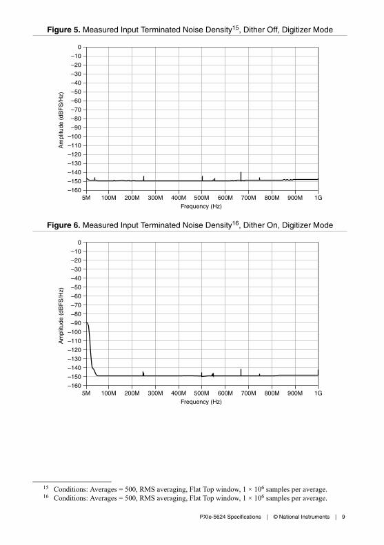
Figure 5. Measured Input Terminated Noise Density15, Dither Off, Digitizer Mode
5M 100M 200M 300M 400M 500M 600M 700M 800M 900M –160
–150
–140
–130
–120
–110
–100
–60
–50
–30
–10
0
Frequency (Hz)
Am
plitu
de (
dBF
S/H
z)
1G
–90
–80
–70
–20
–40
Figure 6. Measured Input Terminated Noise Density16, Dither On, Digitizer Mode
5M 100M 200M 300M 400M 500M 600M 700M 800M 900M –160
–150
–140
–130
–120
–110
–100
–60
–50
–30
–10
0
Frequency (Hz)
Am
plitu
de (
dBF
S/H
z)
1G
–90
–80
–70
–20
–40
15 Conditions: Averages = 500, RMS averaging, Flat Top window, 1 × 10⁶ samples per average.16 Conditions: Averages = 500, RMS averaging, Flat Top window, 1 × 10⁶ samples per average.
PXIe-5624 Specifications | © National Instruments | 9

Spurious Responses
Digitizer ModeEffective number of bits (ENOB), typical17
100 MHz 9.1
410 MHz 9.0
730 MHz 8.8
Signal-to-noise ratio (SNR), typical17
100 MHz 57.5 dB
410 MHz 57 dB
730 MHz 56 dB
Spurious-free dynamic range (SFDR), typical18
50 MHz to 1.5 GHz -72 dBc
1.5 GHz to 2 GHz -70 dBc
48 MHz -77 dBc
100 MHz -79 dBc
185 MHz -80 dBc
410 MHz -75 dBc
650 MHz -75 dBc
730 MHz -74 dBc
925 MHz -74 dBc
Total harmonic distortion (THD), typical19
50 MHz to 1.4 GHz -72 dBc
1.4 GHz to 2 GHz -70 dBc
48 MHz -76 dBc
100 MHz -77 dBc
185 MHz -78 dBc
410 MHz -74 dBc
650 MHz -75 dBc
17 Conditions: Dither off, 8.1 dBm single tone at 100 MHz, 8.3 dBm single tone at 410 MHz,8.7 dBm single tone at 730 MHz, 1,500 Hz resolution bandwidth (RBW).
18 Conditions: Dither on, 5 dBm single tone. SFDR is dominated by second and third harmonics.19 Conditions: Dither on, 5 dBm single tone, second through sixth harmonics.
10 | ni.com | PXIe-5624 Specifications

730 MHz -74 dBc
925 MHz -74 dBc
DDC ModeThird-order intermodulation distortion (IMD3), typical20
50 MHz to 1 GHz -75 dBc
1 GHz to 1.975 GHz -68 dBc
Table 5. Spurious-Free Dynamic Range (SFDR), Typical
Bandwidth (MHz) Center Frequency (MHz) SFDR (dBc)
100 187.5 -9521
400 730 -7622
30 500 -100, nominal
80 500 -100, nominal
100 500 -100, nominal
400 500 -87, nominal
800 500 -87, nominal
DDC out-of-band suppression >85 dB23
DDC frequency shift SFDR -105 dBFS
20 Conditions: Dither on, two -2 dBm tones spaced 1 MHz apart, I/Q rate = 8.75 MHz.21 Conditions: Dither on, I/Q rate = 125 MHz.22 Conditions: Dither on, I/Q rate = 500 MHz.23 Stopband suppression from (0.6 × I/Q rate).
PXIe-5624 Specifications | © National Instruments | 11

Figure 7. Measured Single-Tone Spectrum, 400 MHz Instantaneous Bandwidth, DDCMode24
50M 100M 150M 200M 250M 300M 350M 400M 450M –110
–100
–90
–50
–40
–20
0
8
Frequency (Hz)
Am
plitu
de (
dBm
)
–80
–70
–60
–10
–30
Figure 8. Measured Single-Tone Spectrum, 800 MHz Instantaneous Bandwidth, DDCMode25
100M 200M 300M 400M 500M 600M 700M 800M 900M –100
–90
–80
–50
–40
–20
0
8
Frequency (Hz)
Am
plitu
de (
dBm
)
–70
–60
–10
–30
24 Conditions: Dither on, 500 MHz I/Q rate, 250 MHz frequency shift, 10 kHz noise bandwidth.400 MHz acquisition FPGA image, 5 dBm single-tone input at 100 MHz.
25 Conditions: Dither on, 1 GHz I/Q rate, 500 MHz frequency shift, 20 kHz noise bandwidth,800 MHz acquisition mode FPGA image, 0 dBm single-tone input at 500 MHz.
12 | ni.com | PXIe-5624 Specifications

Figure 9. Measured Two-Tone Spectrum, 187.5 MHz Center Frequency, DDC Mode26
184.3M 185M 186M 187M 188M 189M 190M 190.7M –110
–100
–90
–80
–50
–40
–20
0
8
Frequency (Hz)
Am
plitu
de (
dBm
)
–70
–60
–10
–30
Figure 10. Measured Two-Tone Spectrum, 730 MHz Center Frequency, DDC Mode27
726.8M 727.5M 728.5M 729.5M 730.5M 731.5M 732.5M 733.2M –110
–100
–90
–80
–50
–40
–20
0
8
Frequency (Hz)
Am
plitu
de (
dBm
)
–70
–60
–10
–30
26 Conditions: Dither on, 8 MHz I/Q rate, 187.5 MHz frequency shift, 4 kHz noise bandwidth,400 MHz acquisition FPGA image, input is two -2 dBm tones spaced 1 MHz apart.
27 Conditions: Dither on, 8 MHz I/Q rate, 730 MHz frequency shift, 4 kHz noise bandwidth,400 MHz acquisition FPGA image, input is two -2 dBm tones spaced 1 MHz apart.
PXIe-5624 Specifications | © National Instruments | 13

Error Vector Magnitude (EVM)20 MHz bandwidth 64-QAM EVM28
900 MHz -51.5 dB, nominal
1.8 GHz -50 dB, nominal
Digitizer CharacteristicsResolution 12 bits
Digitizer mode sample rate 2 GS/s
PXI Express Bus PXI Express x8 Gen 2
Onboard FPGAFPGA Xilinx Kintex-7 XC7K410T
Lookup tables (LUT) 254,200
Flip-flops 508,400
DSP48 slices 1,540
Embedded block RAM 28,620 kbits
Data transfers DMA, interrupts, programmed I/O
Number of DMA channels 32
Onboard DRAMMemory size 2 GB
Theoretical maximum data rate 6.4 GB/s
Onboard SRAMMemory size 2 MB
Maximum data rate (read) 26 MB/s
Maximum data rate (write) 20 MB/s
28 Conditions: EVM signal: 20 MHz bandwidth, 64-QAM signal, root-raised cosine pulse shapefiltering, 0.25 alpha, internal Reference Clock source, 300 μs record length, PXIe-5644 used assignal generator, 2 dBm (average) power.
14 | ni.com | PXIe-5624 Specifications

Front Panel I/O
IF INConnector SMA female
Input impedance 50 Ω, nominal
Coupling AC
Absolute maximum input power 20 dBm, continuous wave (CW) RMS
Input return loss/VSWR >15 dB/1.43:129, typical
CLK INConnector SMA female
Frequency
Sample Clock 4 GHz, 2 GHz
Reference Clock 100 MHz, 10 MHz
Tolerance ±50 ppm
Amplitude
10 MHz and 100 MHz ReferenceClocks
-3 dBm to 15 dBm30
2 GHz and 4 GHz Sample Clocks -5 dBm to 10 dBm
Input impedance 50 Ω, nominal
Coupling AC
CLK OUTConnector SMA female
Frequency
Sample Clock 2 GHz
Reference Clock 100 MHz, 10 MHz31
Tolerance Same as Reference Clock or Sample Clocksource32
29 5 MHz to 2 GHz.30 Optimal performance for a 10 MHz Reference Clock is greater than 4 dBm.31 100 MHz available when locking to CLK IN or PXIe_CLK100. 10 MHz available when locking to
external front panel CLK IN.32 Refer to the Internal Frequency Reference section for more information about internal frequency
reference accuracy specifications.
PXIe-5624 Specifications | © National Instruments | 15

Amplitude, typical
Reference Clock (CLK IN) CLK IN input power + 3 dB, nominal
Reference Clock (PXIe_CLK100) 7.5 dBm
Sample Clock 5 dBm
Output impedance 50 Ω, nominal
Coupling AC
PFI 0 (Programmable Function Interface)Connector SMA female
Voltage levels
Absolute maximum input range -0.5 V to 5.5 V
VIL 0.8 V
VIH 2.0 V
VOL 0.2 V with 100 μA load
VOH 2.9 V with 100 μA load
Recommended operating voltage 0 V to 3.3 V
Input impedance 10 kΩ, nominal
Output impedance 50 Ω, nominal
Maximum DC drive strength 24 mA
Minimum required direction changelatency
60 ns + 1 clock cycle33
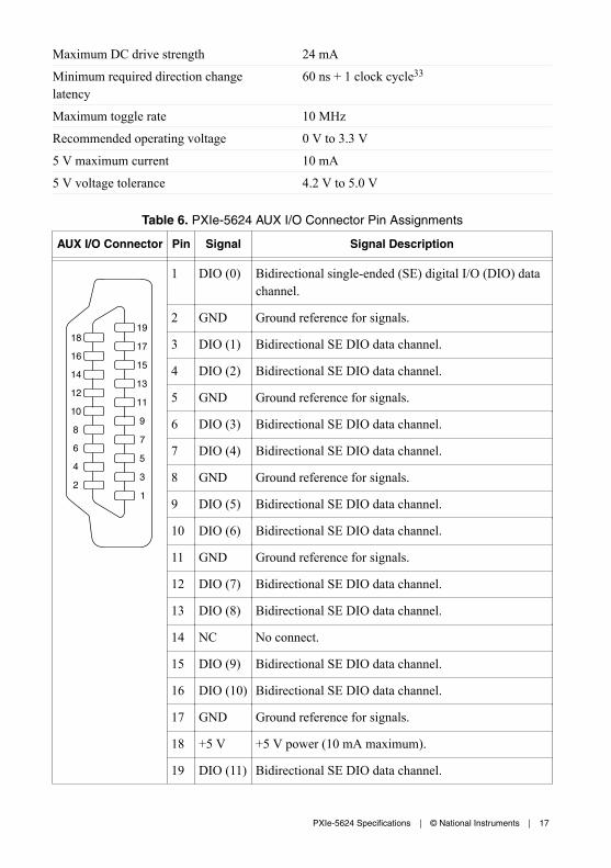
AUX I/OConnector HDMI
Number of channels 12 digital input/output, bi-directional
Voltage levels
Absolute maximum input range -0.5 V to 5.5 V
VIL 0.8 V
VIH 2.0 V
VOL 0.2 V with 100 μA load
VOH 2.9 V with 100 μA load
Input impedance 10 kΩ, nominal
Output impedance 50 Ω, nominal
33 Clock cycle refers to the FPGA clock domain used for direction control.
16 | ni.com | PXIe-5624 Specifications
Maximum DC drive strength 24 mA
Minimum required direction changelatency
60 ns + 1 clock cycle33
Maximum toggle rate 10 MHz
Recommended operating voltage 0 V to 3.3 V
5 V maximum current 10 mA
5 V voltage tolerance 4.2 V to 5.0 V
Table 6. PXIe-5624 AUX I/O Connector Pin Assignments
AUX I/O Connector Pin Signal Signal Description
18
16
14
12
10
8
6
4
2
19
17
1
3
5
7
9
11
13
15
1 DIO (0) Bidirectional single-ended (SE) digital I/O (DIO) datachannel.
2 GND Ground reference for signals.
3 DIO (1) Bidirectional SE DIO data channel.
4 DIO (2) Bidirectional SE DIO data channel.
5 GND Ground reference for signals.
6 DIO (3) Bidirectional SE DIO data channel.
7 DIO (4) Bidirectional SE DIO data channel.
8 GND Ground reference for signals.
9 DIO (5) Bidirectional SE DIO data channel.
10 DIO (6) Bidirectional SE DIO data channel.
11 GND Ground reference for signals.
12 DIO (7) Bidirectional SE DIO data channel.
13 DIO (8) Bidirectional SE DIO data channel.
14 NC No connect.
15 DIO (9) Bidirectional SE DIO data channel.
16 DIO (10) Bidirectional SE DIO data channel.
17 GND Ground reference for signals.
18 +5 V +5 V power (10 mA maximum).
19 DIO (11) Bidirectional SE DIO data channel.
PXIe-5624 Specifications | © National Instruments | 17

Power Requirements
Table 7. Power Requirements34
Voltage (VDC) Typical Current (A) Maximum Current (A)
+3.3 2.45 2.75
+12 1.95 2.2
CalibrationCalibration interval 1 year
Note For a two-year calibration interval, add 0.1 dB to the one-year specificationsfor Absolute Amplitude Accuracy.
Physical CharacteristicsHot Surface If the PXIe-5624 has been in use, it may exceed safe handlingtemperatures and cause burns. Allow the PXIe-5624 to cool before removing it fromthe chassis.
PXIe-5624 module 3U, one slot, PXI Express module
Dimensions 21.6 cm × 2.0 cm × 13.0 cm(8.5 in. × 0.8 in. × 5.1 in.)
Weight 454 g (16.0 oz)
EnvironmentMaximum altitude 2,000 m (800 mbar) (at 25 °C ambient
temperature)
Pollution Degree 2
Indoor use only.
34 Power consumption is 31.5 W, typical. Power consumed depends on FPGA image being used.Power specifications reflect the 400 MHz acquisition FPGA image. Maximum powerconsumption is at highest operating temperature.
18 | ni.com | PXIe-5624 Specifications

Operating EnvironmentAmbient temperature range 0 °C to 55 °C (Tested in accordance with
IEC 60068-2-1 and IEC 60068-2-2. MeetsMIL-PRF-28800F Class 3 low temperaturelimit and MIL-PRF-28800F Class 2 hightemperature limit.)
Relative humidity range 10% to 90%, noncondensing (Tested inaccordance with IEC 60068-2-56.)
Storage EnvironmentAmbient temperature range -40 °C to 71 °C (Tested in accordance
with IEC 60068-2-1 and IEC 60068-2-2. MeetsMIL-PRF-28800F Class 3 limits.)
Relative humidity range 5% to 95%, noncondensing (Tested inaccordance with IEC 60068-2-56.)
Shock and VibrationOperating shock 30 g peak, half-sine, 11 ms pulse (Tested in
accordance with IEC 60068-2-27. MeetsMIL-PRF-28800F Class 2 limits.)
Random vibration
Operating 5 Hz to 500 Hz, 0.3 grms (Tested in accordancewith IEC 60068-2-64.)
Nonoperating 5 Hz to 500 Hz, 2.4 grms (Tested in accordancewith IEC 60068-2-64. Test profile exceeds therequirements of MIL-PRF-28800F, Class 3.)
Compliance and Certifications
SafetyThis product is designed to meet the requirements of the following electrical equipment safetystandards for measurement, control, and laboratory use:• IEC 61010-1, EN 61010-1• UL 61010-1, CSA C22.2 No. 61010-1
Note For UL and other safety certifications, refer to the product label or the OnlineProduct Certification section.
PXIe-5624 Specifications | © National Instruments | 19
Electromagnetic CompatibilityThis product meets the requirements of the following EMC standards for electrical equipmentfor measurement, control, and laboratory use:• EN 61326-1 (IEC 61326-1): Class A emissions; Basic immunity• EN 55011 (CISPR 11): Group 1, Class A emissions• EN 55022 (CISPR 22): Class A emissions• EN 55024 (CISPR 24): Immunity• AS/NZS CISPR 11: Group 1, Class A emissions• AS/NZS CISPR 22: Class A emissions• FCC 47 CFR Part 15B: Class A emissions• ICES-001: Class A emissions
Note In the United States (per FCC 47 CFR), Class A equipment is intended foruse in commercial, light-industrial, and heavy-industrial locations. In Europe,Canada, Australia, and New Zealand (per CISPR 11), Class A equipment is intendedfor use only in heavy-industrial locations.
Note Group 1 equipment (per CISPR 11) is any industrial, scientific, or medicalequipment that does not intentionally generate radio frequency energy for thetreatment of material or inspection/analysis purposes.
Note For EMC declarations, certifications, and additional information, refer to the Online Product Certification section.
CE Compliance This product meets the essential requirements of applicable European Directives, as follows:• 2014/35/EU; Low-Voltage Directive (safety)• 2014/30/EU; Electromagnetic Compatibility Directive (EMC)
Online Product CertificationRefer to the product Declaration of Conformity (DoC) for additional regulatory complianceinformation. To obtain product certifications and the DoC for this product, visit ni.com/certification, search by model number or product line, and click the appropriate link in theCertification column.
Environmental ManagementNI is committed to designing and manufacturing products in an environmentally responsiblemanner. NI recognizes that eliminating certain hazardous substances from our products isbeneficial to the environment and to NI customers.
For additional environmental information, refer to the Minimize Our Environmental Impactweb page at ni.com/environment. This page contains the environmental regulations and
20 | ni.com | PXIe-5624 Specifications
directives with which NI complies, as well as other environmental information not included inthis document.
Waste Electrical and Electronic Equipment (WEEE)EU Customers At the end of the product life cycle, all NI products must bedisposed of according to local laws and regulations. For more information abouthow to recycle NI products in your region, visit ni.com/environment/weee.
电子信息产品污染控制管理办法(中国 RoHS)中国客户 National Instruments 符合中国电子信息产品中限制使用某些有害物
质指令(RoHS)。关于 National Instruments 中国 RoHS 合规性信息,请登录
ni.com/environment/rohs_china。(For information about China RoHScompliance, go to ni.com/environment/rohs_china.)
PXIe-5624 Specifications | © National Instruments | 21

Information is subject to change without notice. Refer to the NI Trademarks and Logo Guidelines at ni.com/trademarks forinformation on NI trademarks. Other product and company names mentioned herein are trademarks or trade names of theirrespective companies. For patents covering NI products/technology, refer to the appropriate location: Help»Patents in yoursoftware, the patents.txt file on your media, or the National Instruments Patent Notice at ni.com/patents. You can findinformation about end-user license agreements (EULAs) and third-party legal notices in the readme file for your NI product. Referto the Export Compliance Information at ni.com/legal/export-compliance for the NI global trade compliance policy and howto obtain relevant HTS codes, ECCNs, and other import/export data. NI MAKES NO EXPRESS OR IMPLIED WARRANTIES ASTO THE ACCURACY OF THE INFORMATION CONTAINED HEREIN AND SHALL NOT BE LIABLE FOR ANY ERRORS. U.S.Government Customers: The data contained in this manual was developed at private expense and is subject to the applicablelimited rights and restricted data rights as set forth in FAR 52.227-14, DFAR 252.227-7014, and DFAR 252.227-7015.
© 2014—2018 National Instruments. All rights reserved.
376298C-01 December 14, 2017