pwm type dc/dc converter ic built-in a switching …the pwm type dc/dc converter for ac/dc provides...
TRANSCRIPT
〇Product structure : Silicon monolithic integrated circuit 〇This product has no designed protection against radioactive rays.
1/19
TSZ02201-0F1F0A200310-1-2
© 2018 ROHM Co., Ltd. All rights reserved. 15.May.2018 Rev.001
TSZ22111 • 14 • 001
www.rohm.com
AC/DC Converter
PWM Type DC/DC Converter IC Built-in a Switching MOSFET BM2P0161 BM2P0361
General Description The PWM type DC/DC converter for AC/DC provides an optimal system for all products that require an electrical outlet. BM2P0xxx supports both isolated and non-isolated devices, enabling simpler design of various types of low power consumption electrical converters. The built-in 650 V starter circuit contributes to low-power consumption. Power supply can be designed flexibly by connecting current sensing resistor for the switching externally. Current is restricted in each cycle and excellent performance is demonstrated in bandwidth and transient response since current mode control is utilized. The switching frequency is 65 kHz. At light load, the switching frequency is reduced and high efficiency is achieved. A frequency hopping function that contributes to low EMI is also included on chip. Design can be easily implemented because includes a 650 V switching MOSFET.
Feature PWM Frequency: 65 kHz PWM Current Mode Control Built-in Frequency Hopping Function Burst Operation When Load is Light Frequency Reduction Function Built-in 650 V Starter Circuit Built-in 650 V Switching MOSFET VCC Pin Under-Voltage Protection VCC Pin Over-Voltage Protection SOURCE Pin Open Protection SOURCE Pin Short Protection SOURCE Pin Leading Edge Blanking Function Per-Cycle Over-Current Protection Circuit Over Current Protection AC Voltage Compensation
Circuit Soft Start Secondary Over-Current Protection Circuit
Key Specification Operating Power Supply Voltage Range:
VCC: 8.9 V to 26.0 V DRAIN: 650 V(Max)
Circuit Current (ON)1: BM2P0161: 0.90 mA(Typ) BM2P0361: 0.65 mA(Typ)
Circuit Current (ON)2: 0.30 mA(Typ) Oscillation Frequency1: 65 kHz(Typ) Operating Ambient Temperature: -40 °C to +105 °C MOSFET ON Resistance:
BM2P0161: 1.0 Ω(Typ) BM2P0361: 3.0 Ω(Typ)
Package W(Typ) x D(Typ) x H(Max)
DIP7K 9.20 mm x 6.35 mm x 4.30 mm pitch 2.54 mm
Application For AC Adapters, TV and Household Appliances (Vacuum Cleaners, Humidifiers, Air Cleaners, Air Conditioners, IH Cooking Heaters, Rice Cookers, etc.)
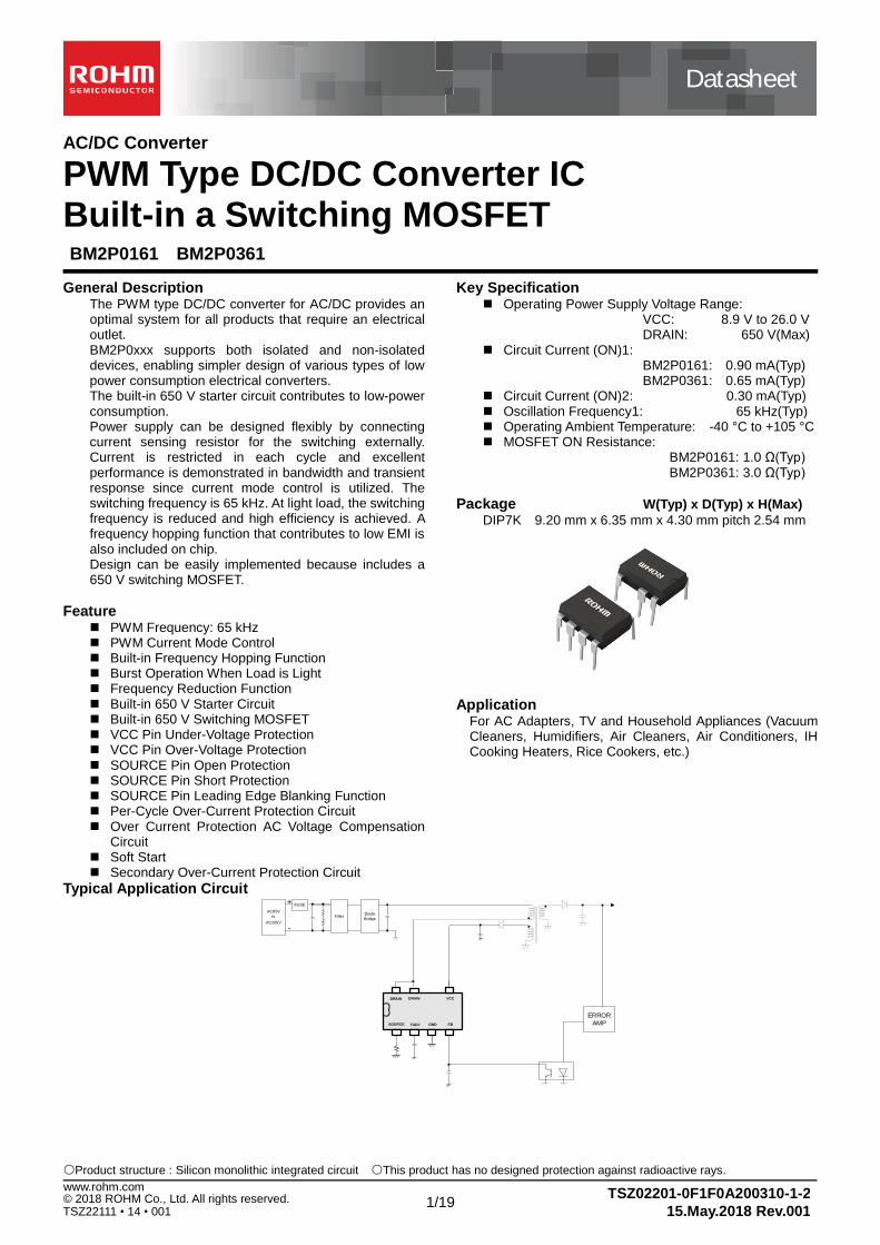
Typical Application Circuit
AC85V
to
AC265V
FUSE+
-
FilterDiode
Bridge
ERROR
AMPGND FBFADJ
VCCDRAIN
SOURCE
DRAIN
Datasheet
2/19
TSZ02201-0F1F0A200310-1-2 © 2018 ROHM Co., Ltd. All rights reserved. 15.May.2018 Rev.001
www.rohm.com
TSZ22111 • 15 • 001
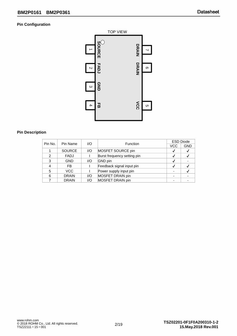
BM2P0161 BM2P0361
Pin Configuration
Pin Description
Pin No. Pin Name I/O Function ESD Diode
VCC GND
1 SOURCE I/O MOSFET SOURCE pin ✔ ✔
2 FADJ I Burst frequency setting pin ✔ ✔
3 GND I/O GND pin ✔ -
4 FB I Feedback signal input pin ✔ ✔
5 VCC I Power supply input pin - ✔
6 DRAIN I/O MOSFET DRAIN pin - -
7 DRAIN I/O MOSFET DRAIN pin - -
GN
D
DR
AIN
DR
AIN
VC
C
SO
UR
CE
76
5
12
34
FA
DJ
FB
TOP VIEW

3/19
TSZ02201-0F1F0A200310-1-2 © 2018 ROHM Co., Ltd. All rights reserved. 15.May.2018 Rev.001
www.rohm.com
TSZ22111 • 15 • 001
BM2P0161 BM2P0361
Block Diagram
Feedback
WithIsolation
AC
FUSE
FilterDiode
Bridge
PWM Control
+
Burst Control
Leading Edge
Blanking
(Typ=250ns)
VCC UVLO
13.5V
/ 8.2V
DRAIN
DRIVER
S
QR
+
-
Current
Limiter
PWMComparator
+
-
+
+
-
BurstComparator
GND
Slope
Compensation
VCC
FB
SOURCE
+
-
30k
+
-
OLP
Internal Block
+-
VCC OVP
27.5V
4.0V
Rs
Soft StartAC Voltage
compensation
OSC(65kHz)
FrequencyHopping
5
4128ms/512msTimer
MAXDUTY
3
1
12V Clamp
Circuit
4.0V
Line Reg
6.7
4.0V
1M
Starter
FADJ
2Burst
Frequency
Control
VH VOUT
10µA
100µs Filter
4/19
TSZ02201-0F1F0A200310-1-2 © 2018 ROHM Co., Ltd. All rights reserved. 15.May.2018 Rev.001
www.rohm.com
TSZ22111 • 15 • 001
BM2P0161 BM2P0361
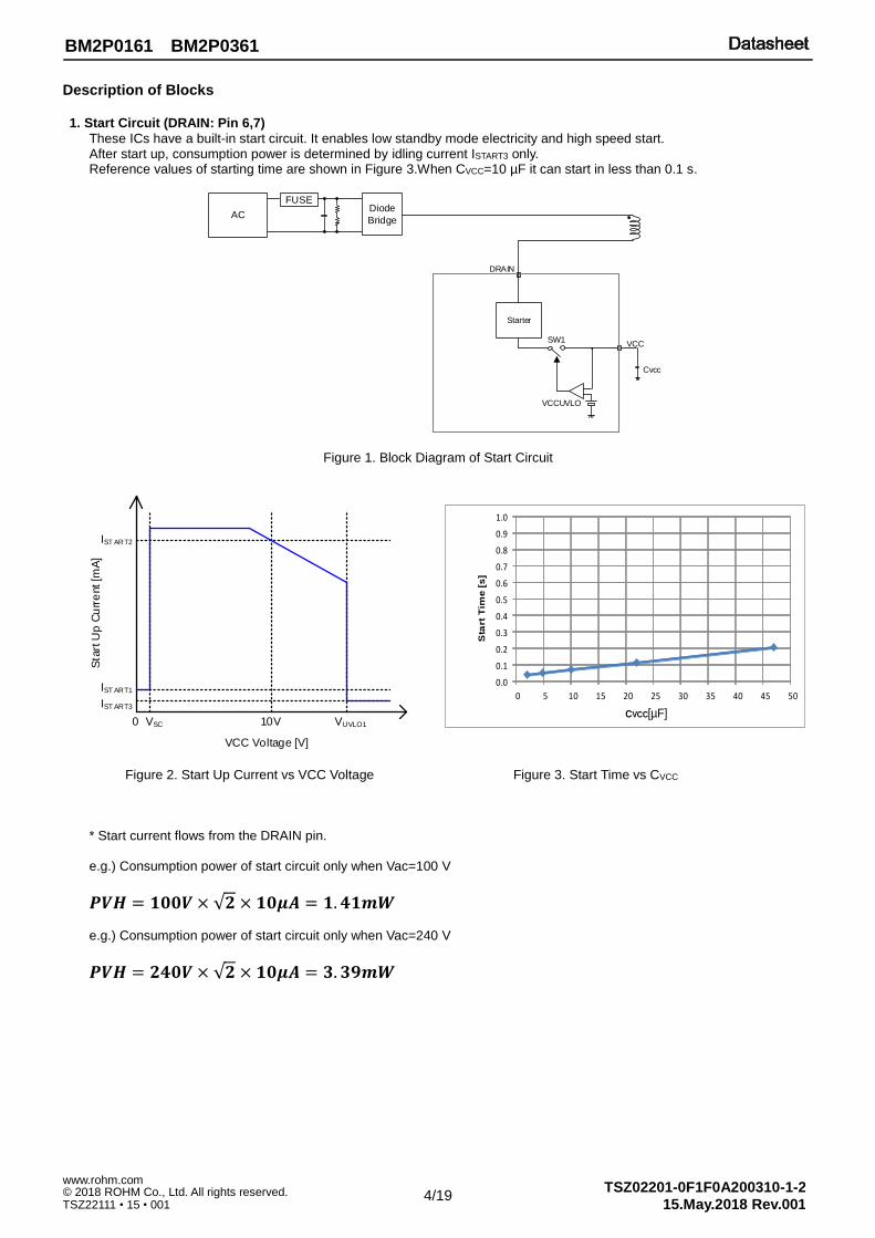
Description of Blocks 1. Start Circuit (DRAIN: Pin 6,7)
These ICs have a built-in start circuit. It enables low standby mode electricity and high speed start. After start up, consumption power is determined by idling current ISTART3 only. Reference values of starting time are shown in Figure 3.When CVCC=10 µF it can start in less than 0.1 s.
Figure 1. Block Diagram of Start Circuit
Figure 2. Start Up Current vs VCC Voltage Figure 3. Start Time vs CVCC
* Start current flows from the DRAIN pin. e.g.) Consumption power of start circuit only when Vac=100 V
𝑷𝑽𝑯 = 𝟏𝟎𝟎𝑽 × √𝟐 × 𝟏𝟎𝝁𝑨 = 𝟏. 𝟒𝟏𝒎𝑾
e.g.) Consumption power of start circuit only when Vac=240 V
𝑷𝑽𝑯 = 𝟐𝟒𝟎𝑽 × √𝟐 × 𝟏𝟎𝝁𝑨 = 𝟑. 𝟑𝟗𝒎𝑾
VCCUVLO
VCC
Starter
Cvcc
DRAIN
FUSEDiode
Bridge
SW1
AC
0 10V VUVLO1VSC
IST ART1
IST ART3
IST ART2
VCC Voltage [V]
Sta
rt U
p C
urr
ent [m
A]
0.0
0.1
0.2
0.3
0.4
0.5
0.6
0.7
0.8
0.9
1.0
0 5 10 15 20 25 30 35 40 45 50
Sta
rt T
ime [
s]
CVCC[µF]

5/19
TSZ02201-0F1F0A200310-1-2 © 2018 ROHM Co., Ltd. All rights reserved. 15.May.2018 Rev.001
www.rohm.com
TSZ22111 • 15 • 001
BM2P0161 BM2P0361
Description of Blocks - continued 2. Start Sequences
Start sequences are shown in Figure 4. See the sections below for detailed descriptions.
Figure 4. Start Sequences Timing Chart
A: Input voltage VH is applied. B: This IC starts operating when VCC>VUVLO1. Switching function starts when other protection functions are judged as
normal. Until the secondary output voltage becomes constant value or more from startup, the VCC pin consumption current causes the VCC voltage to drop. As a result, IC should be set to VCC>VUVLO2 until switching starts.
C: With the soft start function, over current limit value is restricted to prevent any excessive rise in voltage or current. D: When the switching operation starts, VOUT rises. After a switching operating start, set the rated voltage within the tFOLP1 period. E: When there is a light load, it makes FB voltage<VBST. Burst operation is used to keep power consumption down. F: When the FB pin voltage>VFOLP1A, it overloads. G: When the FB pin voltage>VFOLP1A keeps above tFOLP1, overcurrent protection is caused between tFOLP2 period, and
switching stops. If the FB pin voltage<VFOLP1B, the ICs internal timer tFOLP1 is reset. H: If the VCC voltage<VCHG2, recharge operation raises the VCC voltage. I: Same as F. J: Same as G.
Output Voltage
Switching
VH
(Input Voltage)
VCC
FB
Within
128ms
Output Current
Normal
LoadLight
Load
Within
128ms
Over
Load
Within
128msInternal REFPull Up
Burst mode
A BC D E F GH I J
Switchingstop
VUVLO1
VCHG2
VFOLP1A
VUVLO2

6/19
TSZ02201-0F1F0A200310-1-2 © 2018 ROHM Co., Ltd. All rights reserved. 15.May.2018 Rev.001
www.rohm.com
TSZ22111 • 15 • 001
BM2P0161 BM2P0361
Description of Blocks – continued 3. VCC Pin Protection Function
These ICs have a built-in VCC UVLO (Under Voltage Lockout), VCC OVP (Over Voltage Protection), and a VCC recharge function that operates in case of a drop in VCC voltage. VCC charge function stabilizes the secondary output voltage, charged from high voltage lines by the start circuit when VCC voltage drops.
(1) VCC UVLO / VCC OVP Function VCC UVLO and VCC OVP are the self-recovery type comparator having voltage hysteresis.
Figure 5. VCC UVLO / OVP Timing Chart
A: DRAIN voltage inputs, the VCC pin voltage starts rising. B: VCC>VUVLO1, VCC UVLO function is released and DC/DC operation starts. C: VCC<VCHG1, VCC charge function operates and the VCC voltage rises. D: VCC>VCHG2, VCC charge function stops. E: VCC>VOVP1, tLATCH(100 μs Typ) continues, switching is stopped by the VCC OVP function. F: VCC<VOVP2, DC/DC operation restarts. G: VH is OPEN. VCC Voltage falls. H: Same as C. I: Same as D. J: VCC<VUVLO2, VCC UVLO function is detected and DC/DC operation stops.
VCC
Tim
ON
OFF
ON
OFF
OFF
ON
OFF
A B C D F
VH
G H I J A
Tim
ON
ON
OFF
ON
E
OFF
Time
Time
OUT
Switching
VCC UVLO
Function
VCC Charge
Function
VCC OVP
Function
VOVP1
VOVP2
VUVLO1
VUVLO2
VCHG1
VCHG2

7/19
TSZ02201-0F1F0A200310-1-2 © 2018 ROHM Co., Ltd. All rights reserved. 15.May.2018 Rev.001
www.rohm.com
TSZ22111 • 15 • 001
BM2P0161 BM2P0361
3. VCC Pin Protection Function – continued
(2) VCC Charge Function
These ICs have the recharge function. IC starts when the VCC pin voltage>VUVLO1. When VCC voltage becomes VCC<VCHG1 after IC started, VCC recharge function works. At that time the VCC pin is charged from the DRAIN pin through the start circuit. Through this operation, these series prevent failure of VCC startup. When the VCC pin voltage rises until VCC>VCHG2, it finishes recharge. The operation is shown in Figure 6.
Figure 6. VCC Pin Charge Operation
A: The DRAIN pin voltage rises, charges the VCC pin through the VCC charge function. B: VCC>VUVLO1, VCC UVLO function releases, VCC charge function stops, DC/DC operation starts. C: Because output voltage is low, the VCC voltage drops at the start time. D: VCC<VCHG1, VCC recharge function operates, and the VCC pin voltage rise. E: VCC>VCHG2, VCC recharge function stops. F: VCC<VCHG1, VCC recharge function operates, and the VCC pin voltage rise. G: VCC>VCHG2, VCC recharge function stops. H: After the output voltage is finished rising, VCC is charged by the auxiliary winding, and the VCC pin stabilizes.
VCC
VUVLO1
VUVLO2
VCHG1
Switching
VH chargecharge charge
OUTPUT
voltage
VCHG2
charge charge
A B C D E F G H
VH
(Input Voltage)
8/19
TSZ02201-0F1F0A200310-1-2 © 2018 ROHM Co., Ltd. All rights reserved. 15.May.2018 Rev.001
www.rohm.com
TSZ22111 • 15 • 001
BM2P0161 BM2P0361
Description of Blocks – continued
4. DC/DC Driver
These ICs have a current mode PWM control. An internal oscillator sets a fixed switching frequency (65 kHz Typ). It has a switching frequency hopping function, which causes the switching frequency to fluctuate as shown in Figure 7 below. The fluctuation cycle is 125 Hz.(Typ)
Figure 7. Frequency Hopping Function
Maximum duty cycle is fixed at 75 % and minimum ON time is fixed at 400 ns. In current mode control, sub-harmonic oscillation may occur when the duty cycle exceeds 50 %. As a countermeasure, this IC has built-in slope compensation circuits. These ICs have built-in burst mode and frequency reduction circuits to achieve lower power consumption when the load is light. The FB pin is pulled up to an internal power supply by RFB. The FB pin voltage is changed by secondary output voltage (secondary load power). Monitor the FB pin voltage and change a switching operation state. Figure 8 shows the FB voltage, and the DC/DC switching frequency operation. mode1: Burst operation. mode2: Frequency reduction operation. (max frequency is reduced) mode3: Fixed frequency operation. (operates at max frequency) mode4: Overload operation. (stops the pulse operation, sampling operation)
Figure 8. Switching Operation State Changes by FB Pin Voltage
65
SwitchingFrequency
[kHz]
69
125 Hz(8ms)
Time
61
6263
64
66
68
67
500μs
65kHz
25kHz
X
Y
Switching
Frequency
[kHz]
FB [V]0.30V 1.25V 2.00V
mode1 mode2 mode3
2.80V
mode4
Pulse OFF

9/19
TSZ02201-0F1F0A200310-1-2 © 2018 ROHM Co., Ltd. All rights reserved. 15.May.2018 Rev.001
www.rohm.com
TSZ22111 • 15 • 001
BM2P0161 BM2P0361
4. DC/DC Driver – continued (1) Burst Frequency Setting
The frequency can be fixed by adding capacitance to the FADJ pin. This can reduce the burst sounds. The correlation between the capacitor connected to the FADJ pin and frequency is shown in the Figure 10.
Figure 9-1. No setting Figure 9-2. setting
Figure 10. fBST vs CFADJ
Frequency
[kHz]
Output Power[W]
25kHz
Burst
Mode
Frequency
Reduction Mode
Switching
frequency
Burst frequency
Fixed Frequency
Mode
65kHz
[Area of sound]
Frequency
[kHz]
Output Power[W]
25kHz
Burst
Mode
Frequency
Reduction Mode
Switching
frequency
Burst frequency
65kHz
[Area of sound]
FADJ
Fixed Frequency
Mode
CFADJ [pF]
f BS
T [kH
z]
10/19
TSZ02201-0F1F0A200310-1-2 © 2018 ROHM Co., Ltd. All rights reserved. 15.May.2018 Rev.001
www.rohm.com
TSZ22111 • 15 • 001
BM2P0161 BM2P0361
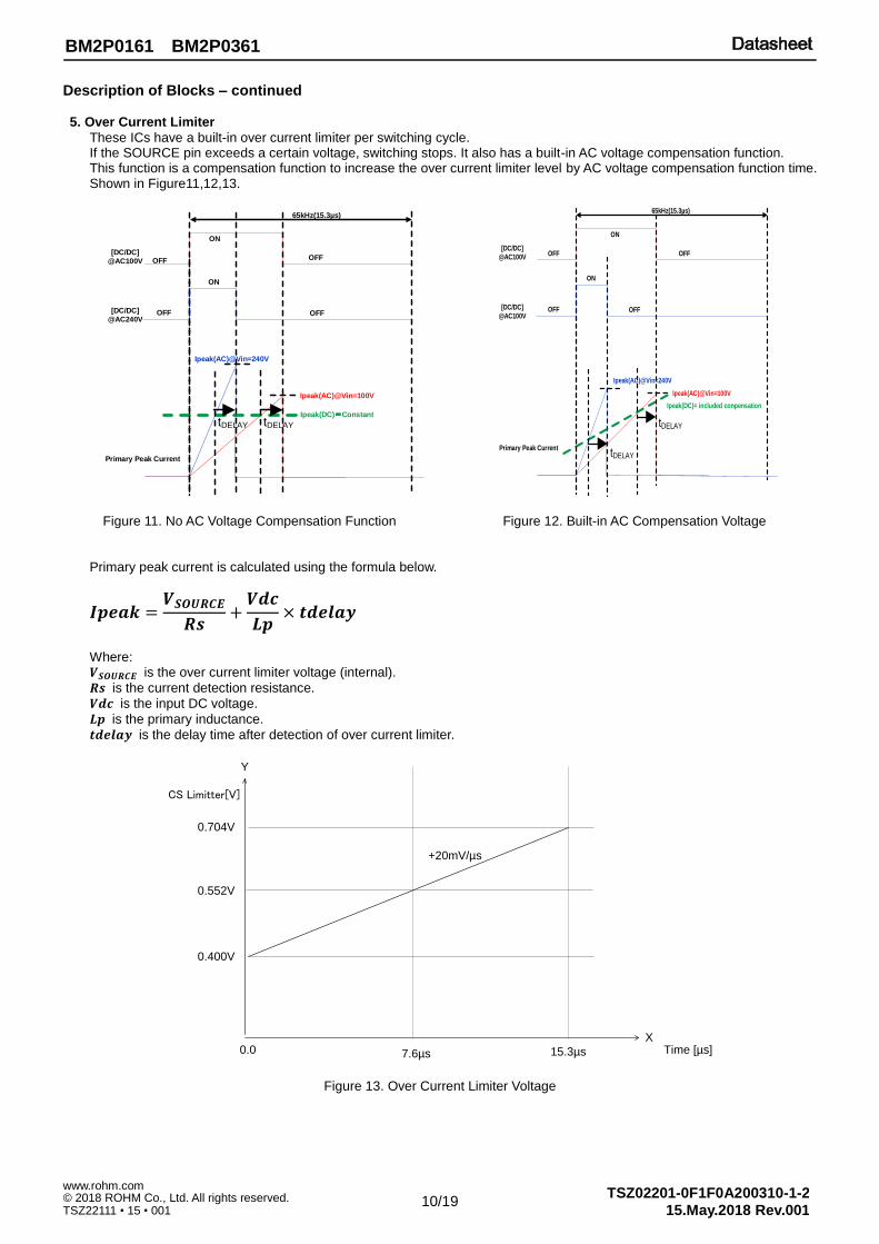
Description of Blocks – continued 5. Over Current Limiter
These ICs have a built-in over current limiter per switching cycle. If the SOURCE pin exceeds a certain voltage, switching stops. It also has a built-in AC voltage compensation function. This function is a compensation function to increase the over current limiter level by AC voltage compensation function time. Shown in Figure11,12,13.
Figure 11. No AC Voltage Compensation Function Figure 12. Built-in AC Compensation Voltage
Primary peak current is calculated using the formula below.
𝑰𝒑𝒆𝒂𝒌 =𝑽𝑺𝑶𝑼𝑹𝑪𝑬𝑹𝒔
+𝑽𝒅𝒄
𝑳𝒑× 𝒕𝒅𝒆𝒍𝒂𝒚
Where: 𝑽𝑺𝑶𝑼𝑹𝑪𝑬 is the over current limiter voltage (internal).
𝑹𝒔 is the current detection resistance.
𝑽𝒅𝒄 is the input DC voltage.
𝑳𝒑 is the primary inductance.
𝒕𝒅𝒆𝒍𝒂𝒚 is the delay time after detection of over current limiter.
Figure 13. Over Current Limiter Voltage
ON
OFFOFF[DC/DC]
@AC100V
Primary Peak Current
Ipeak(DC)=Constant
Ipeak(AC)@Vin=100V
Ipeak(AC)@Vin=240V
ON
OFFOFF[DC/DC]
@AC240V
65kHz(15.3µs)
tDELAY tDELAY
ON
OFFOFF[DC/DC]
@AC100V
Ipeak(DC)= included conpensation
Ipeak(AC)@Vin=100V
Ipeak(AC)@Vin=240V
ON
OFFOFF[DC/DC]
@AC100V
65kHz(15.3µs)
Primary Peak CurrenttDELAY
tDELAY
CS Limitter[V]
X
Y
Time [µs]0.0 15.3µs
0.400V
0.704V
7.6µs
+20mV/µs
0.552V
11/19
TSZ02201-0F1F0A200310-1-2 © 2018 ROHM Co., Ltd. All rights reserved. 15.May.2018 Rev.001
www.rohm.com
TSZ22111 • 15 • 001
BM2P0161 BM2P0361
Description of Blocks – continued 6. L. E. B. Blanking Period
When the MOSFET driver is turned ON, surge current flows through each capacitor component and drive current is generated. Therefore, when the SOURCE pin voltage rises temporarily, detection errors may occur in the over current limiter circuit. To prevent detection errors, DRAIN is switched from high to low and the SOURCE signal is masked for 250 ns by the on-chip LEB (Leading Edge Blanking) function.
7. SOURCE Pin Short Protection Function
When the SOURCE pin is shorted, excessive heat may destroy the IC. To prevent it from being damaged, these ICs have a built-in short protection function.
8. SOURCE Pin Open Protection
When the SOURCE pin becomes OPEN, excessive heat by noise may destroy the IC. To prevent it from being damaged, these ICs have a built-in OPEN protection circuit (auto recovery protection).
9. Output Over Load Protection Function (FB OLP Comparator)
The output overload protection function monitors the secondary output load status at the FB pin and stops switching whenever overload occurs. When there is an overload, the output voltage is reduced and current no longer flows to the photo coupler, so the FB pin voltage rises. When the FB pin voltage >VFOLP1A continuously for the period tFOLP1, it is judged as an overload and switching stops. When the FB pin > VFOLP1A, the voltage goes lower than VFOLP1B during the period tFOLP1, the overload protection timer is reset. The switching operation is performed during this period tFOLP1. At startup, the FB voltage is pulled up to the IC’s internal voltage, so operation starts at a voltage of VFOLP1A or above. Therefore, at startup please set startup time within tFOLP1 so that the FB voltage becomes VFOLP1B or less. Recovery is after the period tFOLP2, from the detection of FBOLP.
Absolute Maximum Ratings (Ta=25 °C)
Parameter Symbol Rating Unit Conditions
Maximum Applied Voltage 1 VMAX1 -0.3 to +32.0 V VCC
Maximum Applied Voltage 2 VMAX2 -0.3 to +6.5 V SOURCE, FB, FADJ
Maximum Applied Voltage 3 VMAX3 650 V DRAIN
Drain Current Pulse IDP 12 A PW=10 μs, Duty cycle=1 % (BM2P0161)
Drain Current Pulse IDP 4 A PW=10 μs, Duty cycle=1 % (BM2P0361)
Power Dissipation Pd 1.00 W (Note 1)
Maximum Junction Temperature Tjmax 150 °C
Storage Temperature Range Tstg -55 to +150 °C Caution 1: Operating the IC over the absolute maximum ratings may damage the IC. The damage can either be a short circuit between pins or an open circuit
between pins and the internal circuitry. Therefore, it is important to consider circuit protection measures, such as adding a fuse, in case the IC is operated
over the absolute maximum ratings. Caution 2: Should by any chance the maximum junction temperature rating be exceeded the rise in temperature of the chip may result in deterioration of the
properties of the chip. In case of exceeding this absolute maximum rating, design a PCB boards with power dissipation taken into consideration by increasing board size and copper area so as not to exceed the maximum junction temperature rating.
(Note 1) When mounted (on 74.2 mm x 74.2 mm, 1.6 mm thick, glass epoxy on single-layer substrate). Reduce to 8 mW/°C when Ta=25 °C or above.

12/19
TSZ02201-0F1F0A200310-1-2 © 2018 ROHM Co., Ltd. All rights reserved. 15.May.2018 Rev.001
www.rohm.com
TSZ22111 • 15 • 001
BM2P0161 BM2P0361
Thermal Loss The thermal design should set operation for the following conditions. 1. The ambient temperature Ta must be 105 °C or less. 2. The IC’s loss must be within the power dissipation Pd. The thermal abatement characteristics are as follows. (PCB: 74.2 mm x 74.2mm x 1.6 mm, mounted on glass epoxy on single-layer substrate)
Figure 14. DIP7K Thermal Abatement Characteristics
Recommended Operating Conditions
Parameter Symbol Rating
Unit Conditions Min Typ Max
Power Supply Voltage Range 1 VCC 8.9 - 26.0 V VCC pin voltage
Power Supply Voltage Range 2 VDRAIN - - 650 V DRAIN pin voltage
Operating Temperature Topr -40 - +105 °C
Electrical Characteristics (unless otherwise noted, Ta=25 °C, VCC=15 V)
Parameter Symbol Rating
Unit Conditions Min Typ Max
[MOSFET Block]
Between Drain and Source Voltage V(BR)DDS 650 - - V ID=1 mA / VGS=0 V
Drain Leak Current IDSS - - 100 μA VDS=650 V / VGS=0 V
On Resistance RDS(ON) - 1.0 1.4 Ω ID=0.25 A / VGS=10 V (BM2P0161)
On Resistance RDS(ON) - 3.0 3.6 Ω ID=0.25 A / VGS=10 V (BM2P0361)
0.0
0.2
0.4
0.6
0.8
1.0
1.2
1.4
0 25 50 75 100 125 150
Pd[W]
Ta[℃]
13/19
TSZ02201-0F1F0A200310-1-2 © 2018 ROHM Co., Ltd. All rights reserved. 15.May.2018 Rev.001
www.rohm.com
TSZ22111 • 15 • 001
BM2P0161 BM2P0361
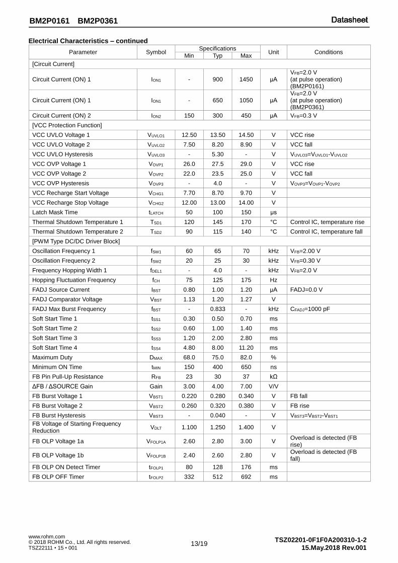
Electrical Characteristics – continued
Parameter Symbol Specifications
Unit Conditions Min Typ Max
[Circuit Current]
Circuit Current (ON) 1 ION1 - 900 1450 μA VFB=2.0 V (at pulse operation) (BM2P0161)
Circuit Current (ON) 1 ION1 - 650 1050 μA VFB=2.0 V (at pulse operation) (BM2P0361)
Circuit Current (ON) 2 ION2 150 300 450 μA VFB=0.3 V
[VCC Protection Function]
VCC UVLO Voltage 1 VUVLO1 12.50 13.50 14.50 V VCC rise
VCC UVLO Voltage 2 VUVLO2 7.50 8.20 8.90 V VCC fall
VCC UVLO Hysteresis VUVLO3 - 5.30 - V VUVLO3=VUVLO1-VUVLO2
VCC OVP Voltage 1 VOVP1 26.0 27.5 29.0 V VCC rise
VCC OVP Voltage 2 VOVP2 22.0 23.5 25.0 V VCC fall
VCC OVP Hysteresis VOVP3 - 4.0 - V VOVP3=VOVP1-VOVP2
VCC Recharge Start Voltage VCHG1 7.70 8.70 9.70 V
VCC Recharge Stop Voltage VCHG2 12.00 13.00 14.00 V
Latch Mask Time tLATCH 50 100 150 μs
Thermal Shutdown Temperature 1 TSD1 120 145 170 °C Control IC, temperature rise
Thermal Shutdown Temperature 2 TSD2 90 115 140 °C Control IC, temperature fall
[PWM Type DC/DC Driver Block]
Oscillation Frequency 1 fSW1 60 65 70 kHz VFB=2.00 V
Oscillation Frequency 2 fSW2 20 25 30 kHz VFB=0.30 V
Frequency Hopping Width 1 fDEL1 - 4.0 - kHz VFB=2.0 V
Hopping Fluctuation Frequency fCH 75 125 175 Hz
FADJ Source Current IBST 0.80 1.00 1.20 μA FADJ=0.0 V
FADJ Comparator Voltage VBST 1.13 1.20 1.27 V
FADJ Max Burst Frequency fBST - 0.833 - kHz CFADJ=1000 pF
Soft Start Time 1 tSS1 0.30 0.50 0.70 ms
Soft Start Time 2 tSS2 0.60 1.00 1.40 ms
Soft Start Time 3 tSS3 1.20 2.00 2.80 ms
Soft Start Time 4 tSS4 4.80 8.00 11.20 ms
Maximum Duty DMAX 68.0 75.0 82.0 %
Minimum ON Time tMIN 150 400 650 ns
FB Pin Pull-Up Resistance RFB 23 30 37 kΩ
ΔFB / ΔSOURCE Gain Gain 3.00 4.00 7.00 V/V
FB Burst Voltage 1 VBST1 0.220 0.280 0.340 V FB fall
FB Burst Voltage 2 VBST2 0.260 0.320 0.380 V FB rise
FB Burst Hysteresis VBST3 - 0.040 - V VBST3=VBST2-VBST1
FB Voltage of Starting Frequency Reduction
VDLT 1.100 1.250 1.400 V
FB OLP Voltage 1a VFOLP1A 2.60 2.80 3.00 V Overload is detected (FB rise)
FB OLP Voltage 1b VFOLP1B 2.40 2.60 2.80 V Overload is detected (FB fall)
FB OLP ON Detect Timer tFOLP1 80 128 176 ms
FB OLP OFF Timer tFOLP2 332 512 692 ms

14/19
TSZ02201-0F1F0A200310-1-2 © 2018 ROHM Co., Ltd. All rights reserved. 15.May.2018 Rev.001
www.rohm.com
TSZ22111 • 15 • 001
BM2P0161 BM2P0361
Electrical Characteristics – continued
Parameter Symbol Specifications
Unit Conditions Min Typ Max
[Over Current Detection Block]
Over-Current Detection Voltage VSOURCE 0.375 0.400 0.425 V tON=0 μs
Over-Current Detection Voltage SS1 VSOURCE_SS1 0.050 0.100 0.150 V 0 ms to tSS1 ms
Over-Current Detection Voltage SS2 VSOURCE_SS2 0.080 0.150 0.220 V tSS1 ms to tSS2 ms
Over-Current Detection Voltage SS3 VSOURCE_SS3 0.130 0.200 0.270 V tSS2 ms to tSS3 ms
Over-Current Detection Voltage SS4 VSOURCE_SS4 0.230 0.300 0.370 V tSS3 ms to tSS4 ms
Leading Edge Blanking Time tLEB 120 250 380 ns (Note 2)
Over Current Detection AC Voltage Compensation Factor
KSOURCE 12 20 28 mV/μs
SOURCE Pin Short Protection Voltage
VSOURCESHT 0.020 0.050 0.080 V
SOURCE Pin Short Protection Time tSOURCESHT 1.80 3.00 4.20 μs
[Circuit Current]
Start Current 1 ISTART1 0.100 0.500 1.000 mA VCC=0 V
Start Current 2 ISTART2 1.000 3.000 6.000 mA VCC=10 V
OFF Current ISTART3 - 10 20 μA
Inflow current from the DRAIN pin after UVLO is released and when MOSFET is OFF
Start Current Switching Voltage VSC 0.800 1.500 2.100 V
(Note 2) Not 100 % tested.
I/O Equivalence Circuit
Figure 15. Equivalence Circuit Diagram
1
DRAIN
2 FADJ
5 VCC - 6-
SOURCE
7
4 FB
SOURCE
VREF
DRAIN
SOURCE
VREF
SOURCE
VCC
GND
GND3
DRAIN
SOURCE
Internal MOSFET
InternalCircuit
DRAIN
SOURCE
Internal MOSFET
InternalCircuit
VCC
RFBFB
Internal Reg
-

15/19
TSZ02201-0F1F0A200310-1-2 © 2018 ROHM Co., Ltd. All rights reserved. 15.May.2018 Rev.001
www.rohm.com
TSZ22111 • 15 • 001
BM2P0161 BM2P0361
Operational Notes 1. Reverse Connection of Power Supply
Connecting the power supply in reverse polarity can damage the IC. Take precautions against reverse polarity when connecting the power supply, such as mounting an external diode between the power supply and the IC’s power supply pins.
2. Power Supply Lines
Design the PCB layout pattern to provide low impedance supply lines. Separate the ground and supply lines of the digital and analog blocks to prevent noise in the ground and supply lines of the digital block from affecting the analog block. Furthermore, connect a capacitor to ground at all power supply pins. Consider the effect of temperature and aging on the capacitance value when using electrolytic capacitors.
3. Ground Voltage
Ensure that no pins are at a voltage below that of the ground pin at any time, even during transient condition. 4. Ground Wiring Pattern
When using both small-signal and large-current ground traces, the two ground traces should be routed separately but connected to a single ground at the reference point of the application board to avoid fluctuations in the small-signal ground caused by large currents. Also ensure that the ground traces of external components do not cause variations on the ground voltage. The ground lines must be as short and thick as possible to reduce line impedance.
5. Recommended Operating Conditions
The function and operation of the IC are guaranteed within the range specified by the recommended operating conditions. The characteristic values are guaranteed only under the conditions of each item specified by the electrical characteristics.
6. Inrush Current
When power is first supplied to the IC, it is possible that the internal logic may be unstable and inrush current may flow instantaneously due to the internal powering sequence and delays, especially if the IC has more than one power supply. Therefore, give special consideration to power coupling capacitance, power wiring, width of ground wiring, and routing of connections.
7. Operation Under Strong Electromagnetic Field
Operating the IC in the presence of a strong electromagnetic field may cause the IC to malfunction. 8. Testing on Application Boards
When testing the IC on an application board, connecting a capacitor directly to a low-impedance output pin may subject the IC to stress. Always discharge capacitors completely after each process or step. The IC’s power supply should always be turned off completely before connecting or removing it from the test setup during the inspection process. To prevent damage from static discharge, ground the IC during assembly and use similar precautions during transport and storage.
9. Inter-pin Short and Mounting Errors
Ensure that the direction and position are correct when mounting the IC on the PCB. Incorrect mounting may result in damaging the IC. Avoid nearby pins being shorted to each other especially to ground, power supply and output pin. Inter-pin shorts could be due to many reasons such as metal particles, water droplets (in very humid environment) and unintentional solder bridge deposited in between pins during assembly to name a few.
10. Unused Input Pins
Input pins of an IC are often connected to the gate of a MOS transistor. The gate has extremely high impedance and extremely low capacitance. If left unconnected, the electric field from the outside can easily charge it. The small charge acquired in this way is enough to produce a significant effect on the conduction through the transistor and cause unexpected operation of the IC. So unless otherwise specified, unused input pins should be connected to the power supply or ground line.

16/19
TSZ02201-0F1F0A200310-1-2 © 2018 ROHM Co., Ltd. All rights reserved. 15.May.2018 Rev.001
www.rohm.com
TSZ22111 • 15 • 001
BM2P0161 BM2P0361
Operational Notes – continued 11. Regarding the Input Pin of the IC
This monolithic IC contains P+ isolation and P substrate layers between adjacent elements in order to keep them isolated. P-N junctions are formed at the intersection of the P layers with the N layers of other elements, creating a parasitic diode or transistor. For example (refer to figure below):
When GND > Pin A and GND > Pin B, the P-N junction operates as a parasitic diode. When GND > Pin B, the P-N junction operates as a parasitic transistor.
Parasitic diodes inevitably occur in the structure of the IC. The operation of parasitic diodes can result in mutual interference among circuits, operational faults, or physical damage. Therefore, conditions that cause these diodes to operate, such as applying a voltage lower than the GND voltage to an input pin (and thus to the P substrate) should be avoided.
Figure 16. Example of monolithic IC structure
12. Ceramic Capacitor
When using a ceramic capacitor, determine a capacitance value considering the change of capacitance with temperature and the decrease in nominal capacitance due to DC bias and others.
13. Area of Safe Operation (ASO)
Operate the IC such that the output voltage, output current, and the maximum junction temperature rating are all within the Area of Safe Operation (ASO).
14. Thermal Shutdown Circuit (TSD)
This IC has a built-in thermal shutdown circuit that prevents heat damage to the IC. Normal operation should always be within the IC’s maximum junction temperature rating. If however the rating is exceeded for a continued period, the junction temperature (Tj) will rise which will activate the TSD circuit that will turn OFF power output pins. When the Tj falls below the TSD threshold, the circuits are automatically restored to normal operation. Note that the TSD circuit operates in a situation that exceeds the absolute maximum ratings and therefore, under no circumstances, should the TSD circuit be used in a set design or for any purpose other than protecting the IC from heat damage.
15. Over Current Protection Circuit (OCP)
This IC incorporates an integrated overcurrent protection circuit that is activated when the load is shorted. This protection circuit is effective in preventing damage due to sudden and unexpected incidents. However, the IC should not be used in applications characterized by continuous operation or transitioning of the protection circuit.
N NP
+ P
N NP
+
P Substrate
GND
NP
+
N NP
+N P
P Substrate
GND GND
Parasitic
Elements
Pin A
Pin A
Pin B Pin B
B C
E
Parasitic
Elements
GNDParasitic
Elements
CB
E
Transistor (NPN)Resistor
N Region
close-by
Parasitic
Elements

17/19
TSZ02201-0F1F0A200310-1-2 © 2018 ROHM Co., Ltd. All rights reserved. 15.May.2018 Rev.001
www.rohm.com
TSZ22111 • 15 • 001
BM2P0161 BM2P0361
Ordering Information
B M 2 P 0 x 6 1
Part No. 1:BM2P0161
3:BM2P0361
Marking Diagram
Product Name Parts Number Marking
BM2P0161 BM2P0161
BM2P0361 BM2P0361
DIP7K (TOP VIEW)
Part Number Marking
LOT Number

18/19
TSZ02201-0F1F0A200310-1-2 © 2018 ROHM Co., Ltd. All rights reserved. 15.May.2018 Rev.001
www.rohm.com
TSZ22111 • 15 • 001
BM2P0161 BM2P0361
Physical Dimension and Packing Information
Package Name DIP7K

19/19
TSZ02201-0F1F0A200310-1-2 © 2018 ROHM Co., Ltd. All rights reserved. 15.May.2018 Rev.001
www.rohm.com
TSZ22111 • 15 • 001
BM2P0161 BM2P0361
Revision History
Date Revision Changes
15.May.2018 001 New Release

Notice-PGA-E Rev.003
© 2015 ROHM Co., Ltd. All rights reserved.
Notice
Precaution on using ROHM Products 1. Our Products are designed and manufactured for application in ordinary electronic equipment (such as AV equipment,
OA equipment, telecommunication equipment, home electronic appliances, amusement equipment, etc.). If you intend to use our Products in devices requiring extremely high reliability (such as medical equipment
(Note 1), transport
equipment, traffic equipment, aircraft/spacecraft, nuclear power controllers, fuel controllers, car equipment including car accessories, safety devices, etc.) and whose malfunction or failure may cause loss of human life, bodily injury or serious damage to property (“Specific Applications”), please consult with the ROHM sales representative in advance. Unless otherwise agreed in writing by ROHM in advance, ROHM shall not be in any way responsible or liable for any damages, expenses or losses incurred by you or third parties arising from the use of any ROHM’s Products for Specific Applications.
(Note1) Medical Equipment Classification of the Specific Applications
JAPAN USA EU CHINA
CLASSⅢ CLASSⅢ
CLASSⅡb CLASSⅢ
CLASSⅣ CLASSⅢ
2. ROHM designs and manufactures its Products subject to strict quality control system. However, semiconductor
products can fail or malfunction at a certain rate. Please be sure to implement, at your own responsibilities, adequate safety measures including but not limited to fail-safe design against the physical injury, damage to any property, which a failure or malfunction of our Products may cause. The following are examples of safety measures:
[a] Installation of protection circuits or other protective devices to improve system safety [b] Installation of redundant circuits to reduce the impact of single or multiple circuit failure
3. Our Products are designed and manufactured for use under standard conditions and not under any special or extraordinary environments or conditions, as exemplified below. Accordingly, ROHM shall not be in any way responsible or liable for any damages, expenses or losses arising from the use of any ROHM’s Products under any special or extraordinary environments or conditions. If you intend to use our Products under any special or extraordinary environments or conditions (as exemplified below), your independent verification and confirmation of product performance, reliability, etc, prior to use, must be necessary:
[a] Use of our Products in any types of liquid, including water, oils, chemicals, and organic solvents [b] Use of our Products outdoors or in places where the Products are exposed to direct sunlight or dust [c] Use of our Products in places where the Products are exposed to sea wind or corrosive gases, including Cl2,
H2S, NH3, SO2, and NO2
[d] Use of our Products in places where the Products are exposed to static electricity or electromagnetic waves [e] Use of our Products in proximity to heat-producing components, plastic cords, or other flammable items [f] Sealing or coating our Products with resin or other coating materials [g] Use of our Products without cleaning residue of flux (even if you use no-clean type fluxes, cleaning residue of
flux is recommended); or Washing our Products by using water or water-soluble cleaning agents for cleaning residue after soldering
[h] Use of the Products in places subject to dew condensation
4. The Products are not subject to radiation-proof design. 5. Please verify and confirm characteristics of the final or mounted products in using the Products. 6. In particular, if a transient load (a large amount of load applied in a short period of time, such as pulse. is applied,
confirmation of performance characteristics after on-board mounting is strongly recommended. Avoid applying power exceeding normal rated power; exceeding the power rating under steady-state loading condition may negatively affect product performance and reliability.
7. De-rate Power Dissipation depending on ambient temperature. When used in sealed area, confirm that it is the use in
the range that does not exceed the maximum junction temperature. 8. Confirm that operation temperature is within the specified range described in the product specification. 9. ROHM shall not be in any way responsible or liable for failure induced under deviant condition from what is defined in
this document.
Precaution for Mounting / Circuit board design 1. When a highly active halogenous (chlorine, bromine, etc.) flux is used, the residue of flux may negatively affect product
performance and reliability.
2. In principle, the reflow soldering method must be used on a surface-mount products, the flow soldering method must be used on a through hole mount products. If the flow soldering method is preferred on a surface-mount products, please consult with the ROHM representative in advance.
For details, please refer to ROHM Mounting specification

Notice-PGA-E Rev.003
© 2015 ROHM Co., Ltd. All rights reserved.
Precautions Regarding Application Examples and External Circuits 1. If change is made to the constant of an external circuit, please allow a sufficient margin considering variations of the
characteristics of the Products and external components, including transient characteristics, as well as static characteristics.
2. You agree that application notes, reference designs, and associated data and information contained in this document
are presented only as guidance for Products use. Therefore, in case you use such information, you are solely responsible for it and you must exercise your own independent verification and judgment in the use of such information contained in this document. ROHM shall not be in any way responsible or liable for any damages, expenses or losses incurred by you or third parties arising from the use of such information.
Precaution for Electrostatic This Product is electrostatic sensitive product, which may be damaged due to electrostatic discharge. Please take proper caution in your manufacturing process and storage so that voltage exceeding the Products maximum rating will not be applied to Products. Please take special care under dry condition (e.g. Grounding of human body / equipment / solder iron, isolation from charged objects, setting of Ionizer, friction prevention and temperature / humidity control).
Precaution for Storage / Transportation 1. Product performance and soldered connections may deteriorate if the Products are stored in the places where:
[a] the Products are exposed to sea winds or corrosive gases, including Cl2, H2S, NH3, SO2, and NO2 [b] the temperature or humidity exceeds those recommended by ROHM [c] the Products are exposed to direct sunshine or condensation [d] the Products are exposed to high Electrostatic
2. Even under ROHM recommended storage condition, solderability of products out of recommended storage time period may be degraded. It is strongly recommended to confirm solderability before using Products of which storage time is exceeding the recommended storage time period.
3. Store / transport cartons in the correct direction, which is indicated on a carton with a symbol. Otherwise bent leads
may occur due to excessive stress applied when dropping of a carton. 4. Use Products within the specified time after opening a humidity barrier bag. Baking is required before using Products of
which storage time is exceeding the recommended storage time period.
Precaution for Product Label A two-dimensional barcode printed on ROHM Products label is for ROHM’s internal use only.
Precaution for Disposition When disposing Products please dispose them properly using an authorized industry waste company.
Precaution for Foreign Exchange and Foreign Trade act Since concerned goods might be fallen under listed items of export control prescribed by Foreign exchange and Foreign trade act, please consult with ROHM in case of export.
Precaution Regarding Intellectual Property Rights 1. All information and data including but not limited to application example contained in this document is for reference
only. ROHM does not warrant that foregoing information or data will not infringe any intellectual property rights or any other rights of any third party regarding such information or data.
2. ROHM shall not have any obligations where the claims, actions or demands arising from the combination of the Products with other articles such as components, circuits, systems or external equipment (including software).
3. No license, expressly or implied, is granted hereby under any intellectual property rights or other rights of ROHM or any third parties with respect to the Products or the information contained in this document. Provided, however, that ROHM will not assert its intellectual property rights or other rights against you or your customers to the extent necessary to manufacture or sell products containing the Products, subject to the terms and conditions herein.
Other Precaution 1. This document may not be reprinted or reproduced, in whole or in part, without prior written consent of ROHM.
2. The Products may not be disassembled, converted, modified, reproduced or otherwise changed without prior written consent of ROHM.
3. In no event shall you use in any way whatsoever the Products and the related technical information contained in the Products or this document for any military purposes, including but not limited to, the development of mass-destruction weapons.
4. The proper names of companies or products described in this document are trademarks or registered trademarks of ROHM, its affiliated companies or third parties.

DatasheetDatasheet
Notice – WE Rev.001© 2015 ROHM Co., Ltd. All rights reserved.
General Precaution 1. Before you use our Products, you are requested to carefully read this document and fully understand its contents.
ROHM shall not be in any way responsible or liable for failure, malfunction or accident arising from the use of any ROHM’s Products against warning, caution or note contained in this document.
2. All information contained in this document is current as of the issuing date and subject to change without any prior
notice. Before purchasing or using ROHM’s Products, please confirm the latest information with a ROHM sales representative.
3. The information contained in this document is provided on an “as is” basis and ROHM does not warrant that all
information contained in this document is accurate and/or error-free. ROHM shall not be in any way responsible or liable for any damages, expenses or losses incurred by you or third parties resulting from inaccuracy or errors of or concerning such information.

Datasheet
Part Number BM2P0161Package DIP7KUnit Quantity 2000Minimum Package Quantity 2000Packing Type TubeConstitution Materials List inquiryRoHS Yes
BM2P0161 - Web Page