pwm as a low cost method for the analog control of mems
TRANSCRIPT

JOURNAL OF MICROELECTROMECHANICAL SYSTEMS, VOL. 28, NO. 2, APRIL 2019 245
PWM as a Low Cost Method for the AnalogControl of MEMS Devices
Corey Pollock , Lawrence K. Barrett , Pablo G. del Corro , Alexander Stange ,Thomas G. Bifano, and David J. Bishop
Abstract— In this paper, we discuss the use of pulse widthmodulation (PWM) to control analog MEMS devices. We achievea precise linear analog control of MEMS by applying PWMsignal with a frequency well above the system’s mechanicalnatural frequency. We first demonstrate this using a parallelplate actuator and comb-drive, and then extend the techniqueto control a commercial deformable mirror. Such an approachallows the system designer to replace expensive drive electronicssuch as the high precision DACs and high voltage, linearamplifiers with a simple on-off switch. The advancements in theelectronics industry tend to make precise timing cheaper andfaster; our approach exploits these long-term trends to createlow-cost control circuits. We also show how PWM control canlinearize the positional response of the devices, where typicallythe position would depend quadratically on the applied analogvoltage.
Index Terms— Microelectromechanical systems, pulse widthmodulation, electrostatic actuator, linearize.
I. INTRODUCTION
M ICROELECTROMECHANICAL systems (MEMS)have become a technological solution of choice for
many advanced applications and currently are a roughly$20B/year industry. They are small, fast, and robust witha wide range of sensing and actuating capabilities. Usingsemiconductor manufacturing methods, they can be quiteinexpensive to build. One broad class of MEMS use actuatorsto achieve mechanical motion in response to applied electricalinputs. Examples include micromirrors [1]–[3], shutters [4],valves [5], RF filters [6], [7], nanopositioners [8]–[11]and atomic writing systems [12]. MEMS actuators
Manuscript received August 24, 2018; revised November 2, 2018; acceptedDecember 23, 2018. Date of publication January 14, 2019; date of currentversion April 2, 2019. This work was supported in part by the Engineer-ing Research Centers Program of the National Science Foundation underNSF Cooperative Agreement EEC-0812056, in part by the DARPA Atomsto Products (A2P) Program/Air Force Research Laboratory (AFRL) underContract FA8650-15-C-7545, in part by the National Science Foundationunder NSF Cooperative Agreement ECCS-1708283, and in part by theEngineering Research Centers Program of the National Science Foundationunder NSF Cooperative Agreement EEC-1647837. Subject Editor A. Zhang.(Corresponding author: Corey Pollock.)
C. Pollock and T. G. Bifano are with the Mechanical Engineering Depart-ment, Boston University, Boston, MA 02215 USA (e-mail: [email protected]).
L. K. Barrett and A. Stange are with the Materials Science and EngineeringDivision, Boston University, Boston, MA 02215 USA.
P. G. del Corro is with the Laboratoire de l’Intégration du Matériau auSystéme, Université de Bordeaux, 33600 Pessac, France.
D. J. Bishop is with the Materials Science and Engineering Division,Mechanical Engineering Department, Department of Electrical and ComputerEngineering, Department of Physics, Department of Biomedical Engineering,Boston University, Boston, MA 02215 USA.
Digital Object Identifier 10.1109/JMEMS.2019.2891205
can be built using a wide range of driving methodsincluding electrostatic [13]–[16], electromagnetic [17], [18],thermal [19]–[21] and piezoelectric [22] techniques. Someactuators are digital, the presence or absence of a signalturns something on or off, but most require analog control.A deformable mirror (DM) is an example requiring analogcontrol where the surface shape of a deformable membraneis distorted by a spatially distributed array of actuators tochange the wavefront of reflected light.
In electrostatic and piezoelectric devices, the control signalis usually a high voltage, low current signal, typically in the50-250 volt range. Thermal devices normally use a few volts ofdrive at a few tens of milliamps of current and electromagneticdrives might require a volt or two at hundreds of millamps. Theelectronic circuits for controlling MEMS devices have specialrequirements, well beyond typical analog circuits, and can beexpensive. For many electrostatic systems, there is a digitalcontrol system (usually a microprocessor), a high precisionDigital to Analog converter (DAC) and a linear, high voltage(HV) amplifier. These drive circuits need high precision andmodest speeds. It is not uncommon in a commercial device forthe drive electronics to be far more expensive than the MEMSchip itself, severely restricting MEMS as a low cost solution.
Pulse width modulation (PWM) is a drive technique thatuses pulses of varying widths to achieve analog control. It iscommonly used to control the speed of DC motors but it hasalso been used to control MEMS such as the dimming ina optical system [23], [24], the flow through a microfluidicvalve [5], [25], and to control thermal actuators [26]. Such adrive scheme has a number of advantages over conventionalapproaches. In an electrostatic system, one can replace theprecision DAC and linear HV amplifier with a simple on-offswitch. Timing is digital and cheap, whereas analog controlis not. The electronics industry continues to research anddevelop faster transistors [27]–[30], and PWM control canleverage these gains. Given that most systems are controlledwith a microprocessor, the timing essentially comes for freeand integrating a DC power supply and HV switch completesthe control circuit. As an example, with a 1 kHz MEMS deviceand a 1 GHz processor, one can use a 10 kHz PWM drive withnanosecond timing control to provide the equivalent of a 17 bitDAC. Another advantage, as we show below, is that PWMlinearizes the response of the system. Typically, the positionof an electrostatic device depends quadratically on appliedvoltage whereas for PWM control, the position is a quasi linearfunction of duty cycle.
1057-7157 © 2019 IEEE. Translations and content mining are permitted for academic research only. Personal use is also permitted,but republication/redistribution requires IEEE permission. See http://www.ieee.org/publications_standards/publications/rights/index.html for more information.

246 JOURNAL OF MICROELECTROMECHANICAL SYSTEMS, VOL. 28, NO. 2, APRIL 2019
This paper investigates the use of PWM to control threedifferent analog electrostatic MEMS systems, (1) a singleparallel plate mass sensor, (2) a comb-drive actuator usedfor writing with atomic beams, and (3) a commerical DMthat can be reshaped dynamically using an array of parallelplate actuators. Although similar PWM methods have beenused [31]–[34], this work focuses on the analog controland the cost savings of this technique. We first present thetheoretical derivation of PWM control and the linearizationof the electrostatic devices. Then we analyze and discuss theresults from the three systems. While this paper focuses onelectrostatic drives, the PWM approach is general and worksequally well with any type of drive (e.g. thermal, piezoelectric,magnetic).
II. THEORY
This work investigates two types of electrostatic actuators,(1) a parallel plate capacitor and (2) a comb-drive. This sectiondescribes the theory of using PWM to drive these actuators.A graphic model for each system is shown in Fig. 1, both ofwhich can be approximated as linear systems described by thedifferential equation:
mx + bx + kx = F(t), (1)
where m is mass, b is the damping coefficient, k is the springconstant, x is position, x is velocity, x is acceleration, and F(t)is an externally applied force. Throughout this work we drivethe MEMS with a PWM signal (i.e. pulse wave, rectangularwave) switching between zero force and a maximum force, F0,at a frequency, ω. We demonstrate in this section that if ω ismuch greater than the system’s natural frequency, the effectiveforce on the mass becomes F0 RDC , where RDC is the dutycycle (value 0-1). The Fourier series of the forcing functiondescribed above is:
F(t) = F0 RDC + F0
∞∑
n=1
2
nπsin(nπ RDC)cos(nωt), (2)
where F(t) is the force, t is time (seconds) and ω is frequency(rad/s). This can be separated into two forces, F1 and F2,defined as:
F1 = F0 RDC , (3)
F2 = F0
∞∑
n=1
2
nπsin(nπ RDC)cos(nωt). (4)
The response of a linear system may be represented as thesuperposition of responses from multiple force inputs. This isdescribed mathematically as x(t) = x1 + x2, where x1 and x2are the position responses of F1 and F2 respectively. We firstinvestigate x2. F2 is the summation of sinusoidal forces andone method of solving the steady state solution of a sinusoidalinput is to use the transfer function of the system, with thesolution being equal to the sinusoidal input times the transferfunction. The transfer function of a mass spring system is [35]:
x
F(t)= 1
m√
(ω2n − (ω)2)2 + (2ζωnω)2
, (5)
where ωn =√
km is the natural frequency of the system and
ζ = 2ωnb . We can then multiply the transfer function by each
summation term in (4). When making this step, we mustalso substitute ω with nω, since nω is the frequency in eachsummation term. Therefore the position response of F2 is:
x2 = F0
∞∑
n=1
2
nπ
sin(nπ RDC)cos(nωt)
m√
(ω2n − (nω)2)2 + (2ζωnnω)2
. (6)
Next we look at the response from F1, which we can plugdirectly into (1). Since we are solving for the steady statesolution x = x = 0 and we are left with only the opposingspring force. This results in:
x1 = F0 RDC
k. (7)
From (6) we see that if ω >> ωn , the sinusoidal response,x2, approaches zero. This agrees with the known frequencyresponse of a harmonic oscillator. As the driving frequencyincreases beyond the natural frequency, the amplitude of theresponse decreases by 40 dB/decade. This means that if wedrive a mass with a PWM signal at a frequency much greaterthan the natural frequency, x2 goes to zero and we are leftwith (7) defining our steady state solution. This solution istrue for all linear mass spring damper systems driven by aPWM signal.
Conceptually, imagine hitting a child’s swing with baseballs.If the frequency of baseballs hitting the swing is comparableto or below the swing’s natural frequency, the swing willmove appreciably between impacts of the ball. However, if theballs hit the swing at a rate far in excess of the swing’snatural frequency, the swing stays in a static position. Therelaxation of the swing’s position is negligible in comparisonwith its static displacement. By changing the specific impulsetransferred to the swing, its position can be continuouslycontrolled in exactly the same way one would control itsposition by adjusting an analog force.
Next, we look at the specific cases of the electrostaticactuators where we substitute F0 with the electrostatic force,Fe. In this case, we use a PWM signal for the voltagewhich then produces a PWM signal for the electrostatic force.One of the assumptions in the above equations is that theforce is switching instantaneously. To extend these results tothe electrostatic force, the electrical response time of theseactuators must be much faster than the period of the PWMsignal. The fastest frequency we use is 2 MHz. The parallelplate capacitors and comb-drives we test have an electricaltime constant, (τ ), less than a nanosecond. This is much fasterthan the period of our signal and therefore we can assume theelectrostatic force matches the PWM signal.
The first actuator we will look at is a parallel plate capacitor.In general, the electrostatic force across a capacitor is:
Fe = 1
2
dC
dxV 2, (8)
Using a parallel plates model, the electrostatic force betweentwo plates is [36]:
Fe = � AV 2
2(g0 − x)2 , (9)

POLLOCK et al.: PWM AS A LOW COST METHOD FOR THE ANALOG CONTROL OF MEMS DEVICES 247
Fig. 1. Electrostatic Actuator Models: a) Parallel plate capacitor where A is the plate area and g0 is the gap between the plates. b) Comb-drive actuatorwhere t is the comb thickness (out of plane) and g is the lateral gap (perpendicular to x) between comb fingers. In both figures m is the mass of the movableplate or combs, k is the spring constant, x is the displacement, and V is the applied voltage difference.
where � is the medium’s permittivity, A is the area of the plate,V is the PWM voltage, g0 is the pre-actuation gap between thestationary and moving plates and x is the displacement of themoving plate. When controlling the displacement of the platewith voltage control, the plate initially has a quadratic responsewith respect to voltage for small values of x . However, asx approaches 1/3 of g0 (pull-in position [37]), the responsedeviates from a quadratic curve and dx
dV approaches infinity,resulting in an unstable system. When this same system isdriven with a PWM signal, the resulting force on the massis Fe RDC , with V 2 constant. With this change, the response isnow linear with respect to the duty cycle for small values of x .With a constant force, the position would be truly linear withrespect to the duty cycle, however in the case of the parallelplate capacitor, the force, Fe, changes with displacement.As x approaches the pull-in position, the response becomesnonlinear and eventually becomes unstable, similar to theresponse of a conventional analog control.
We now turn our attention to a comb-drive. If we againassume a parallel plate model, the electrostatic force is [36]:
Fe = �ntV 2
g, (10)
where n is the number of interdigitated fingers, t is the combthickness, and g is the gap between the fingers. One of theglaring differences between the comb-drive and parallel plateis that there is no x term in the comb-drive force. This meansthe force does not depend on the displacement and with a con-stant voltage, V , Fe is constant. This leads to a linear solutionto (7) with respect to the duty cycle. By simply changingthe method of control from voltage to PWM, we effectivelylinearize the system. It is worth noting that (10) is subjectto error because fringe field effects contribute significantly tothe capacitance of the device. Although the predicted forceand capacitance are low, we show in the subsequent sectionthat the predicted linear relationship is still accurate.
In general, PWM can be used in conjunction with a low passfilter to provide smooth precise analog control of a MEMSsystem. One method is to use the force generating system asa filter. This is how many thermal MEMS are driven withPWM [26]. In this scenario the thermal system is slower thanthe PWM frequency and acts as a low pass filter, resulting
TABLE I
STEADY STATE TESTING SUMMARY
in an analog temperature and therefore an analog mechanicalresponse. The method discussed in this paper and describedmathematically above uses a force (electric field) that respondsfaster than the PWM frequency but is applied to a slowermechanical system. This results in the mechanical systemacting as the low pass filter. For this last scenario the systemmust meet two requirements: (1) the force (e.g. electric field,magnetic field, temperature) must have a response time muchfaster than the PWM driving frequency and (2) the drivingfrequency must be much faster than the mechanical naturalfrequency.
III. RESULTS AND DISCUSSION
In this section we describe each of the three MEMS devicesin detail and discuss their experimental results. The firstis a parallel plate capacitor, an electrostatic, out of plane,trampoline-type device. The second is a comb-drive linear in-plane actuator. These two fit the models presented in Fig. 1well and provide a test bed for the theory discussed above.The final device is a commercial MEMS device, a DMmanufactured by Boston Micromachines Corporation. Due tothe geometry of the DM, it does not match the linear modelas well, however we show that it can still be effectively drivenwith PWM. Each device has different setup requirements andwe cover each in detail in the subsequent sections. The setupsare also summarized in Table I.
A. Parallel Plate Actuator
Fig. 2a shows a scanning electron microscope (SEM) imageof the parallel plate actuator. It was made using the Poly-MUMPs process from MEMSCAP. The actuator consists of
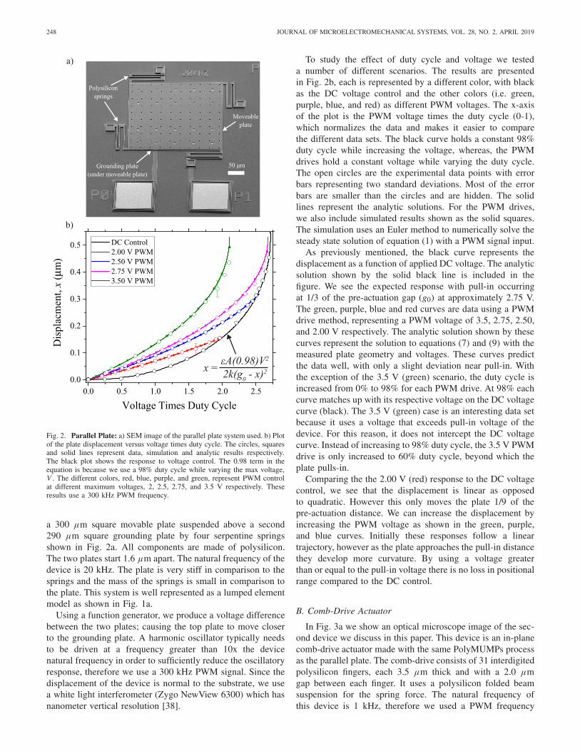
248 JOURNAL OF MICROELECTROMECHANICAL SYSTEMS, VOL. 28, NO. 2, APRIL 2019
Fig. 2. Parallel Plate: a) SEM image of the parallel plate system used. b) Plotof the plate displacement versus voltage times duty cycle. The circles, squaresand solid lines represent data, simulation and analytic results respectively.The black plot shows the response to voltage control. The 0.98 term in theequation is because we use a 98% duty cycle while varying the max voltage,V . The different colors, red, blue, purple, and green, represent PWM controlat different maximum voltages, 2, 2.5, 2.75, and 3.5 V respectively. Theseresults use a 300 kHz PWM frequency.
a 300 μm square movable plate suspended above a second290 μm square grounding plate by four serpentine springsshown in Fig. 2a. All components are made of polysilicon.The two plates start 1.6 μm apart. The natural frequency of thedevice is 20 kHz. The plate is very stiff in comparison to thesprings and the mass of the springs is small in comparison tothe plate. This system is well represented as a lumped elementmodel as shown in Fig. 1a.
Using a function generator, we produce a voltage differencebetween the two plates; causing the top plate to move closerto the grounding plate. A harmonic oscillator typically needsto be driven at a frequency greater than 10x the devicenatural frequency in order to sufficiently reduce the oscillatoryresponse, therefore we use a 300 kHz PWM signal. Since thedisplacement of the device is normal to the substrate, we usea white light interferometer (Zygo NewView 6300) which hasnanometer vertical resolution [38].
To study the effect of duty cycle and voltage we testeda number of different scenarios. The results are presentedin Fig. 2b, each is represented by a different color, with blackas the DC voltage control and the other colors (i.e. green,purple, blue, and red) as different PWM voltages. The x-axisof the plot is the PWM voltage times the duty cycle (0-1),which normalizes the data and makes it easier to comparethe different data sets. The black curve holds a constant 98%duty cycle while increasing the voltage, whereas, the PWMdrives hold a constant voltage while varying the duty cycle.The open circles are the experimental data points with errorbars representing two standard deviations. Most of the errorbars are smaller than the circles and are hidden. The solidlines represent the analytic solutions. For the PWM drives,we also include simulated results shown as the solid squares.The simulation uses an Euler method to numerically solve thesteady state solution of equation (1) with a PWM signal input.
As previously mentioned, the black curve represents thedisplacement as a function of applied DC voltage. The analyticsolution shown by the solid black line is included in thefigure. We see the expected response with pull-in occurringat 1/3 of the pre-actuation gap (g0) at approximately 2.75 V.The green, purple, blue and red curves are data using a PWMdrive method, representing a PWM voltage of 3.5, 2.75, 2.50,and 2.00 V respectively. The analytic solution shown by thesecurves represent the solution to equations (7) and (9) with themeasured plate geometry and voltages. These curves predictthe data well, with only a slight deviation near pull-in. Withthe exception of the 3.5 V (green) scenario, the duty cycle isincreased from 0% to 98% for each PWM drive. At 98% eachcurve matches up with its respective voltage on the DC voltagecurve (black). The 3.5 V (green) case is an interesting data setbecause it uses a voltage that exceeds pull-in voltage of thedevice. For this reason, it does not intercept the DC voltagecurve. Instead of increasing to 98% duty cycle, the 3.5 V PWMdrive is only increased to 60% duty cycle, beyond which theplate pulls-in.
Comparing the the 2.00 V (red) response to the DC voltagecontrol, we see that the displacement is linear as opposedto quadratic. However this only moves the plate 1/9 of thepre-actuation distance. We can increase the displacement byincreasing the PWM voltage as shown in the green, purple,and blue curves. Initially these responses follow a lineartrajectory, however as the plate approaches the pull-in distancethey develop more curvature. By using a voltage greaterthan or equal to the pull-in voltage there is no loss in positionalrange compared to the DC control.
B. Comb-Drive Actuator
In Fig. 3a we show an optical microscope image of the sec-ond device we discuss in this paper. This device is an in-planecomb-drive actuator made with the same PolyMUMPs processas the parallel plate. The comb-drive consists of 31 interdigitedpolysilicon fingers, each 3.5 μm thick and with a 2.0 μmgap between each finger. It uses a polysilicon folded beamsuspension for the spring force. The natural frequency ofthis device is 1 kHz, therefore we used a PWM frequency

POLLOCK et al.: PWM AS A LOW COST METHOD FOR THE ANALOG CONTROL OF MEMS DEVICES 249
Fig. 3. Comb-Drive: a) Optical microscope image of the comb-drive systemused. b) Plot of the comb displacement versus voltage times duty cycle.The circles and solid lines represent data and analytic results respectively.The black plot shows the response to voltage control. The 0.90 term in theequation is because we use a 90% duty cycle while varying the max voltage,V . The different colors, red, blue, purple, and green, represent PWM control atdifferent maximum voltages, 20, 30, 40, and 50 V respectively. These resultsuse a 50 kHz PWM frequency.
of 50 kHz. This system is well represented by our comb-drivemodel in Fig. 1b.
Unlike the parallel plate actuator, this device has a pull-involtage close to 40 V. To generate the higher voltages, we usea high speed, HV amplifier (Trek 2100HF) to amplify theoutput of a function generator. Comb-drives move laterallyin-plane, therefore we can use an optical microscope to imageand measure the displacement of the movable fingers.
We use a similar approach to study the effect of duty cycleand voltage on the comb-drive as we do with the parallel plate.The results are shown in Fig. 3b. Again, each color representsa different driving scenario with black as the DC voltagecontrol and the other colors (i.e. green, purple, blue and red)as different PWM voltages. The DC voltage curve holds aconstant 90% duty cycle while increasing the voltage, whereas,the PWM drives hold a constant voltage while varying the dutycycle. The open circles are the experimental data points andthe solid lines represent the analytic solutions.
The analytic solutions use equation (8) instead of equation(10) due to the aforementioned fringe field effects. We use an
Fig. 4. Low Cost Switching Circuit: Simplified diagram of the N-channelMOSFET gate driver based circuit implemented to drive the DM using a highvoltage PWM signal. We use a 92 V battery as the voltage source.
optical microscope to measure the comb-drive geometry anduse these measurements in Comsol Multiphysics to simulatea value for dC/dx . This method accounts for both fringefield effects and the well known levitation effect [39]–[41],neither of which is captured by equation (10). It is worthnoting that the analytic solutions shown in Fig. 3b use a singleconstant value for dC/dx . We also use Comsol simulate thespring constant of the comb-drive’s folded beam suspension.The spring constant value is decreased 22% to best matchthe data. We attribute the difference largely to errors in themeasurements of beam width and differences in materialproperties between our actual device and simulation.
The DC voltage control is represented by black, with thesolid black line representing the analytic solution, which isincluded in the figure. We see the expected quadratic positionresponse in Fig. 3b. Again we normalize the data by plottingthe voltages times the duty cycle. The pull-in voltage anddistance is less easily defined for the comb-drive comparedto the parallel plate because it typically occurs due to eitherasymmetries in the device or small perturbations while actu-ating [36], both of which are difficult to predict. Nonetheless,we are able to experimentally determine that the pull-in voltagefor the comb-drive is approximately 40 V. The green, purple,blue, and red represent a 50, 40, 30, and 20 V PWM signalrespectively. The solid lines represent the solution to equations(7) and (10) with the measured geometry and voltage. As wesee in Fig. 3b the theory predicts the linear response well.With the exception of the 50 V case (green), we increase theduty cycle from 0% to 90% for each PWM drive. At 90%each curve matches up with its respective voltage on the DCcontrol curve. The 50 V scenario again is noteworthy as ituses a PWM voltage which exceeds the pull-in voltage of thedevice. Therefore it does not match up with a data point onthe voltage control curve. Instead the 50 V case increases from0% to 60% duty cycle. Increasing the duty cycle beyond 60%causes the comb-drive to pull-in.
Unlike the parallel plate actuator, the position response ofthe comb-drive with respect to duty cycle is completely linearthroughout the full range of motion, regardless of position ordriving voltage. We can see why by examining equation (10).The force on the comb-drive does not change with position.By switching a constant force on and off, the response is linearwith respect to the duty cycle. Like the parallel plate, there isno loss of motion in the actuator when using a PWM voltagegreater than or equal to the pull-in voltage.
250 JOURNAL OF MICROELECTROMECHANICAL SYSTEMS, VOL. 28, NO. 2, APRIL 2019
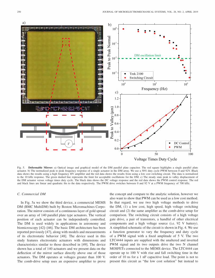
Fig. 5. Deformable Mirror: a) Optical image and graphical model of the DM parallel plate capacitor. The red square highlights a single parallel plateactuator. b) The normalized peak to peak frequency response of a single actuator in the DM array. We use a 50% duty cycle PWM between 0 and 92V. Blackdata shows the results using a high frequency HV amplifier and the red data shows the results from using a low cost switching circuit. The data is normalizedto the 10 kHz response. The green dashed line represents the limit for acceptable oscillations for the DM. c) The steady state peak to valley displacement ofthe DM actuator versus voltage times duty cycle. The black data shows the DC voltage response and the red data shows the PWM control response. The redand black lines are linear and quadratic fits to the data respectively. The PWM drive switches between 0 and 92 V at a PWM frequency of 700 kHz.
C. Commercial DM
In Fig. 5a we show the third device, a commercial MEMSDM (BMC MultiDM) built by Boston Micromachines Corpo-ration. The mirror consists of a continuous layer of gold spreadover an array of 140 parallel plate type actuators. The verticalposition of each actuator can be independently controlled.The DM is used widely in applications in astronomy andbiomicroscopy [42]–[46]. The basic DM architecture has beenreported previously [47], along with models and measurementsof its electrostatic behavior [48]. The device used in thisstudy features electrostatic actuators with dimensions andcharacteristics similar to those described in [49]. The deviceshown has a total of 140 actuators and we present data on thedeflection of the mirror surface directly above one of thoseactuators. The DM operates at voltages greater than 100 V.The comb-drive setup uses an expensive amplifier to prove
the concept and compare to the analytic solution, however wealso want to show that PWM can be used as a low cost method.In that regard, we use two high voltage methods to drivethe DM, (1) a low cost, high speed, high voltage switchingcircuit and (2) the same amplifier as the comb-drive setup forcomparison. The switching circuit consists of a high voltagegate drive, a pair of transistors, a handful of other electricalcomponents and a high voltage source (i.e. 92 V battery).A simplified schematic of the circuit is shown in Fig. 4. We usea function generator to vary the frequency and duty cycleof a PWM signal with a fixed amplitude of 5 V. The twoLTC4444 inputs are supplied with the unaltered and invertedPWM signal and its two outputs drive the two N channelMOSFETs connected to the MEMS device. The LTC4444 canoperate up to 100 V with rise and fall switching time in theorder of 10 ns for a 1 nF capacitive load. The point is not topresent this circuit as “the low cost solution” but instead to

POLLOCK et al.: PWM AS A LOW COST METHOD FOR THE ANALOG CONTROL OF MEMS DEVICES 251
provide an example of how PWM can be implemented cheaplyto drive a high voltage electrostatic MEMS device. Althoughwe use a computer and function generator to produce the PWMsignal in this experiment, these could be replaced by a cheapmicroprocessor or a field programmable gate array.
We first test the frequency response of the DM using boththe Trek 2100HF amplifier and our switching circuit to providea 50% duty cycle PWM signal switching between 0 and92 V. We use a Polytec vibrometer to measure the velocityof the piston mode actuation and integrate this to get a dis-placement. Testing the frequency response accomplishes twothings: (1) it compares the switching circuit to the amplifierto ensure similar results and (2) provides a measurement ofthe oscillation amplitude. To operate properly the normalizedoscillation amplitude needs to be less than 0.01 and we canexperimentally determine the necessary frequency. Fig. 5bshows that the performance of the switching circuit andamplifier are comparable. This gives us confidence movingforward that we can use the switching circuit in place ofthe amplifier. Fig. 5b also shows that the oscillation of theDM drops below the amplitude limit at 700 kHz. We use thisfrequency to demonstrate the steady state response.
For the steady state response, we use the white lightinterferometer to measure the vertical displacement of themirror. Fig. 5c shows a central result of this paper. The DCvoltage control is shown in black with data points as solidblack squares and the solid line is a quadratic fit to the data.Here we use a 100% duty cycle and increase the voltage to95 V. The PWM data is shown in red circles and the red line isa linear fit. The PWM drive uses a 92 V signal and increasesfrom 0% to 88% duty cycle. Fig. 5c shows that this curveintercepts the voltage control at the respective voltage. At thisvoltage, the response of the actuator is linear with respect toduty cycle. The pull-in voltage of this actuator is upwardsof 200 V. The linear response using a 92 V PWM voltagecorrelates well with the results from the first device where wesee a linear response at voltages lower than pull-in.
The results from these three devices summarize the advan-tages of the PWM drive method: (1) PWM can map out theentire response curve of the conventional analog approach, (2)the response can be a linear function of duty cycle, eliminatingthe standard non-linear response one finds with analog controland (3) by using a high voltage switch instead of a DACand a linear HV amplifier, one can control the device withtiming, not analog control. Although we use a HV amplifierto demonstrate the capability and limitations of the PWM withthe comb-drive device, this could be replaced by a low costswitching circuit similar to the one shown in Fig. 4. Thecurrent electronics circuit to control the DM is a majorityof the system price, with the components for each channelcosting approximately $10. Using quantities comparable tothe commercial DM, we estimate the components for thecircuit in Fig. 4 to cost approximately $3.00/channel, ∼3times less expensive. For the DM in this work, which has140 channels, that is a $980 cheaper. The main reason forthis lower cost is because the circuit uses components that aremanufactured at a larger quantity. A HV linear amplifier is amore specialized component than a HV transistor; this results
in lower manufacturing volumes and higher prices. Such acost reduction is significant and opens up the application spacefor the use of such DM systems. The main limitation to thePWM approach is that it excites the mechanical modes ofthe system. However, these oscillations can be reduced to anacceptable level by increasing the drive frequency as shownin Fig. 5b. With advancements in the electronics industry,PWM continues to get faster, cheaper, and easier to implement.
IV. CONCLUSION
In this paper we discussed the use of a PWM signal tocontrol analog MEMS devices compared to the conventionalmethod. We demonstrated that by applying a PWM signal toa MEMS device at frequencies well above the device naturalfrequency, one can achieve precise, analog control. This canbe done with no loss in range compared to the conven-tional analog approach and allows system designers to replaceexpensive electronic components such as high precision DACsand HV linear amplifiers with a low cost switching circuit.In addition, research and development into transistors by theelectronics industry continues to improve transistor speeds andthis approach exploits these long term trends to create lowcost control circuits. We have also demonstrated how it canlinearize the positional response of devices where typically theposition would depend quadratically on the applied, analogvoltage.
ACKNOWLEDGMENT
The author Prof. T. G. Bifano acknowledges a financialinterest in Boston Micromachines Corporation, which pro-duced some of the hardware test devices that were studiedin this work.
REFERENCES
[1] J. Morrison, M. Imboden, T. D. C. Little, and D. J. Bishop, “Elec-trothermally actuated tip-tilt-piston micromirror with integrated varifocalcapability,” Opt. Express, vol. 23, no. 7, pp. 9555–9566, 2015.
[2] S. T. S. Holmström, U. Baran, and H. Urey, “MEMS laser scanners:A review,” J. Microelectromech. Syst., vol. 23, no. 2, pp. 259–275,2014.
[3] D. M. Marom et al., “Wavelength-selective 1 × K switches using free-space optics and MEMS micromirrors:Theory, design, and implementa-tion,” J. Lightw. Technol., vol. 23, no. 4, pp. 1620–1630, Apr. 2005.
[4] M. J. Li et al., “Microshutter array system for james webb spacetelescope,” Proc. SPIE, vol. 6687, p. 668709, Sep. 2007. [Online].Available: https://www.spiedigitallibrary.org/conference-proceedings-of-spie/6687/668709/Microshutter-array-system-for-James-Webb-Space-Telescope/10.1117/12.734152.full?SSO=1
[5] J. Collier, D. Wroblewski, and T. Bifano, “Development of a rapid-response flow-control system using MEMS microvalve arrays,” J. Micro-electromech. Syst., vol. 13, no. 6, pp. 912–922, Dec. 2004.
[6] K. Entesari and G. M. Rebeiz, “A 12-18-GHz three-pole RF MEMStunable filter,” IEEE Trans. Microw. Theory Techn., vol. 53, no. 8,pp. 2566–2571, Aug. 2005.
[7] K. Chen, X. Liu, A. Kovacs, W. J. Chappell, and D. Peroulis, “Antibiasedelectrostatic RF MEMS varactors and tunable filters,” IEEE Trans.Microw. Theory Techn., vol. 58, no. 12, pp. 3971–3981, Dec. 2010.
[8] X. Liu, K. Kim, and Y. Sun, “A MEMS stage for 3-axis nanoposition-ing,” J. Micromech. Microeng., vol. 17, no. 9, pp. 1796–1802, 2007.
[9] Q. Yao, J. Dong, and P. M. Ferreira, “Design, analysis, fabrication andtesting of a parallel-kinematic micropositioning XY stage,” Int. J. Mach.Tools Manuf., vol. 47, no. 6, pp. 946–961, 2007.
[10] M. Maroufi, A. G. Fowler, and S. O. R. Moheimani, “MEMS fornanopositioning: Design and applications,” J. Microelectromech. Syst.,vol. 26, no. 3, pp. 469–500, Jun. 2017.
[11] P. G. del Corro, M. Imboden, and D. J. Pérez, D. J. Bishop, andH. Pastoriza, “Single ended capacitive self-sensing system for combdrives driven XY nanopositioners,” Sens. Actuators A, Phys., vol. 271,pp. 409–417, Mar. 2018.

252 JOURNAL OF MICROELECTROMECHANICAL SYSTEMS, VOL. 28, NO. 2, APRIL 2019
[12] M. Imboden et al., “Atomic calligraphy: The direct writing of nanoscalestructures using a microelectromechanical system,” Nano Lett., vol. 13,no. 7, pp. 3379–3384, 2013.
[13] J. D. Grade, H. Jerman, and T. W. Kenny, “Design of large deflectionelectrostatic actuators,” J. Microelectromech. Syst., vol. 12, no. 3,pp. 335–343, Jun. 2003.
[14] J. I. Seeger and B. E. Boser, “Charge control of parallel-plate, elec-trostatic actuators and the tip-in instability,” J. Microelectromech. Syst.,vol. 12, no. 5, pp. 656–671, Oct. 2003.
[15] G. N. Nielson and G. Barbastathis, “Dynamic pull-in of parallel-plateand torsional electrostatic MEMS actuators,” J. Microelectromech. Syst.,vol. 15, no. 4, pp. 811–821, Aug. 2006.
[16] R. Yeh, S. Hollar, and K. S. J. Pister, “Single mask, large force, and largedisplacement electrostatic linear inchworm motors,” J. Microelectro-mech. Syst., vol. 11, no. 4, pp. 330–336, Aug. 2002.
[17] S. Imai and T. Tsukioka, “A magnetic MEMS actuator using a permanentmagnet and magnetic fluid enclosed in a cavity sandwiched by polymerdiaphragms,” Precis. Eng., vol. 38, no. 3, pp. 548–554, 2014.
[18] D. Niarchos, “Magnetic MEMS: Key issues and some applications,”Sens. Actuators A, Phys., vol. 106, nos. 1–3, pp. 255–262, 2003.
[19] J. H. Comtois and V. M. Bright, “Applications for surface-micromachined polysilicon thermal actuators and arrays,” Sens. Actu-ators A, Phys., vol. 58, no. 1, pp. 19–25, 1997.
[20] Q.-A. Huang and N. K. S. Lee, “Analysis and design of polysilicon ther-mal flexure actuator,” J. Micromech. Microeng., vol. 9, no. 1, pp. 64–70,1999. [Online]. Available: papers2://publication/uuid/6267D293-24DE-4C18-A4B2-365734E9D23A
[21] D. Yan, A. Khajepour, and R. Mansour, “Design and modeling of aMEMS bidirectional vertical thermal actuator,” J. Micromech. Microeng.,vol. 14, no. 7, pp. 841–850, 2004.
[22] N. Ledermann et al., “1 0 0-Textured, piezoelectric Pb(Zrx , Ti1−x )O3thin films for MEMS: Integration, deposition and properties,” Sens. Actu-ators A, Phys., vol. 105, no. 2, pp. 162–170, 2003.
[23] P. F. van Kessel, L. J. Hornbeck, R. E. Meier, and M. R. Douglass,“A MEMS-based projection display,” Proc. IEEE, vol. 86, no. 8,pp. 1687–1704, Aug. 1998.
[24] L. Svilainis, “LED brightness control for video display applica-tion,” Displays, vol. 29, no. 5, pp. 506–511, 2008, doi: 10.1016/j.displa.2008.05.002.
[25] B. Bae et al., “Feasibility test of an electromagnetically driven valveactuator for glaucoma treatment,” J. Microelectromech. Syst., vol. 11,no. 4, pp. 344–354, Aug. 2002.
[26] J. T. Butler, V. M. Bright, and W. D. Cowan, “Average power control andpositioning of polysilicon thermal actuators,” Sens. Actuators A, Phys.,vol. 72, no. 1, pp. 88–97, 1999.
[27] M. T. Bohr and I. A. Young, “CMOS scaling trends and beyond,” IEEEMicro, vol. 37, no. 6, pp. 20–29, Nov./Dec. 2017.
[28] G. S. Tulevski et al., “Toward high-performance digital logic technologywith carbon nanotubes,” ACS Nano, vol. 8, no. 9, pp. 8730–8745, 2014.
[29] T. N. Theis and P. M. Solomon, “In quest of the ‘next switch’: Prospectsfor greatly reduced power dissipation in a successor to the silicon field-effect transistor,” Proc. IEEE, vol. 98, no. 12, pp. 2005–2014, Dec. 2010.
[30] P. Carbone, S. Kiaei, and F. Xu, Design, Modeling and Testing ofData Converters. Berlin, Germany: Springer-Verlag, 2014. [Online].Available: http://www.springer.com/series/4748
[31] C. Pollock et al., “Engineered PWM drives for achieving rapid step andsettle times for MEMS actuation,” J. Microelectromech. Syst., vol. 27,no. 3, pp. 513–520, 2018.
[32] J.-F. Saheb, J.-F. Richard, M. Sawan, R. Meingan, and Y. Savaria,“System integration of high voltage electrostatic MEMS actuators,”Analog Integr. Circuits Signal Process., vol. 53, no. 1, pp. 27–34,2007.
[33] S. Heinz et al., “High-voltage amplifier design for MEMS basedswitching arrays in wavelength-division multiplexing networks,” in Proc.IEEE Int. Symp. Ind. Electron., Jun. 2007, pp. 1418–1423.
[34] J. Wu and L. R. Carley, “Electromechanical �� modulation with high-Q micromechanical accelerometers and pulse density modulated forcefeedback,” IEEE Trans. Circuits Syst. I, Reg. Papers, vol. 53, no. 2,pp. 274–287, Feb. 2006.
[35] B. H. Tongue, Principles of Vibration, 2nd ed. New York, NY, USA:Oxford Univ. Press, 2002.
[36] M. I. Younis, MEMS Linear and Nonlinear Statics and Dynamics. NewYork, NY, USA: Springer, 2011.
[37] W.-M. Zhang, H. Yan, Z.-K. Peng, and G. Meng, “Electrostatic pull-in instability in MEMS/NEMs: A review,” Sens. Actuators A, Phys.,vol. 214, pp. 187–218, Aug. 2014.
[38] Newview 6300 Specifications, Zygo, Berwyn, PA, USA, 2005.
[39] W. C. Tang, M. G. Lim, and R. T. Howe, “Electrostatic comb drivelevitation and control method,” J. Microelectromech. Syst., vol. 1, no. 4,pp. 170–178, Dec. 1992.
[40] M. Imboden, J. Morrison, E. Lowell, H. Han, and D. J. Bishop,“Controlling levitation and enhancing displacement in electrostatic combdrives of MEMS actuators,” J. Microelectromech. Syst., vol. 23, no. 5,pp. 1063–1072, Oct. 2014.
[41] P. G. del Corro, M. Imboden, D. J. Bishop, and H. Pastoriza, “Combdrive designs with minimized levitation,” J. Microelectromech. Syst.,vol. 25, no. 6, pp. 1025–1032, 2016.
[42] T. Bifano, “Adaptive imaging MEMS deformable mirrors,” NaturePhoton., vol. 5, no. 1, pp. 21–23, 2011, doi: 10.1038/nphoton.2010.297.
[43] W. J. Shain, N. A. Vickers, B. B. Goldberg, T. Bifano, and J. Mertz,“Extended depth-of-field microscopy with a high-speed deformablemirror,” Opt. Lett., vol. 42, no. 5, pp. 995–998, 2017. [Online]. Available:https://www.osapublishing.org/abstract.cfm?URI=ol-42-5-995
[44] D. Sinefeld, H. P. Paudel, D. G. Ouzounov, T. G. Bifano, andC. Xu, “Adaptive optics in multiphoton microscopy: Compari-son of two, three and four photon fluorescence,” Opt. Express,vol. 23, no. 24, pp. 31472–31483, 2015. [Online]. Available:https://www.osapublishing.org/abstract.cfm?URI=oe-23-24-31472
[45] J. Li, T. G. Bifano, and J. Mertz, “Widefield fluorescence microscopywith sensor-based conjugate adaptive optics using oblique back illumi-nation,” Proc. SPIE, vol. 21, no. 12, p. 121504, 2016.
[46] B. Macintosh et al., “The gemini planet imager: First light,” Proc. Nat.Acad. Sci. USA, vol. 111, no. 35, pp. 2661–2666, 2014.
[47] T. G. Bifano, J. Perreault, R. K. Mali, and M. N. Horenstein, “Micro-electromechanical deformable mirrors,” IEEE J. Sel. Topics QuantumElectron., vol. 5, no. 1, pp. 83–89, Jan./Feb. 1999.
[48] M. N. Horenstein, T. G. Bifano, R. K. Mali, and N. Vandelli,“Electrostatic effects in micromachined actuators for adaptive optics,”J. Electrostatics, vol. 42, pp. 69–81, Oct. 1997.
[49] S. A. Cornelissen, P. A. Bierden, T. G. Bifano, and C. L. V. Lam,“4096-element continuous face-sheet MEMS deformable mirror forhigh-contrast imaging,” Proc. SPIE, vol. 8, no. 3, p. 031308, 2009.
Corey Pollock received the B.S. degree in mechan-ical engineering from the University of Washingtonin 2010, and the M.S. degree in mechanical engi-neering from Boston University in 2017, where heis currently pursuing the Ph.D. degree in mechanicalengineering, as a member of Dr. David Bishop’sGroup. His research involves MEMS technology,specifically studying micro mirrors and smart light-ing applications.
Lawrence K. Barrett received the B.S. degree inapplied physics, and the M.S. degree in physicsfrom Brigham Young University in 2014 and 2015,respectively. He is currently pursuing the Ph.D.degree in materials science and engineering withBoston University. His research interests includeMEMS design and control, nanomanufacturing, car-bon nanotubes, graphene, and advanced chemicalvapor deposition techniques.
Pablo G. del Corro received the B.S. degree in elec-tronic engineering from the Universidad Nacionalde Santiago del Estero, Argentina, in 2012, andthe Ph.D. diploma degree in engineering sciencesfrom Instituto Balseiro, Argentina, in 2017. HisPh.D. thesis was focused on the design and char-acterization of MEMS devices and control circuitimplementation for a MEMS-based 3D printing sys-tem. He held post-doctoral positions at BordeauxUniversity, France, in 2018. His research focuseson using MEMS for sensing and energy harvestingapplications.
POLLOCK et al.: PWM AS A LOW COST METHOD FOR THE ANALOG CONTROL OF MEMS DEVICES 253
Alexander Stange received the B.Sc. degree inphysics from McGill University in 2012, and theM.Sc. in Engineering degree in nanotechnology fromthe University of Pennsylvania in 2016. He is cur-rently pursuing the Ph.D. degree with the MaterialScience Division, Boston University (BU). At BU,he is currently researching the Casimir Effect usingMEMS accelerometers and superconducting cavities.He is a member of the American Physical Societyand the Materials Research Society.
Thomas G. Bifano received the B.S. and M.S.degrees in mechanical engineering and materialsscience from Duke University, Durham, NC, USA,and the Ph.D. degree in mechanical engineeringfrom North Carolina State University, Raleigh, NC,USA. He is currently a Professor of mechanicalengineering with Boston University, Boston, MA,USA, with joint appointment as a Professor withthe Department of Biomedical Engineering and theDivision of Materials Science and Engineering. Hisresearch focuses on development of microelectro-
mechanical systems for optical and biomedical applications. He joined BostonUniversity in 1988. He directs the Boston University Photonics Center,and is also the Co-Founder and the Chief Technology Officer of BostonMicromachines Corporation.
David J. Bishop received the B.S. degree in physicsfrom Syracuse University, and the M.S. and Ph.D.degrees in physics from Cornell University. He wasthe Interim Associate Dean for Research and Gradu-ate Programs at the College of Engineering, BostonUniversity (BU). Before joining BU in 2011, he wasthe Chief Technology Officer, and also the ChiefOperating Officer of LGS. Prior to joining LGS, hewas the President of the Government Research &Security Solutions for Bell Labs, Lucent Technolo-gies. He is currently the Director of the CELL-MET
NSF Engineering Research Center, and the Head of the Division of MaterialsScience and Engineering, Boston University. He is also a Professor of physics,Professor of electrical and computer engineering, Professor of materialsscience and engineering, and a Professor of mechanical engineering. Heis a Bell Labs Fellow. In his previous positions with Lucent, he servedas the Nanotechnology Research VP for Bell Labs, Lucent Technologies,the President of the New Jersey Nanotechnology Consortium, and the PhysicalSciences Research VP.