pulsar: towards a synthesis flow for qdi circuits
TRANSCRIPT
PONTIFICAL CATHOLIC UNIVERSITY OF RIO GRANDE DO SULSCHOOL OF TECHNOLOGY
COMPUTER SCIENCE GRADUATE PROGRAM
PULSAR: TOWARDS ASYNTHESIS FLOW FOR QDI
CIRCUITS
MARCOS LUIGGI LEMOS SARTORI
Dissertation submitted to the PontificalCatholic University of Rio Grande do Sulin partial fullfillment of the requirementsfor the degree of Master in ComputerScience.
Advisor: Prof. Dr. Ney Laert Vilar CalazansCo-Advisor: Dr. Matheus Trevisan Moreira
Porto Alegre2019


REPLACE THIS PAGE WITHTHE LIBRARY CATALOG
PAGE


REPLACE THIS PAGE WITHTHE COMMITTEE FORMS


To those I love,


“Creativity Is Intelligence Having Fun.”(Albert Einstein)

PULSAR: EM DIREÇÃO A UM FLUXO DE SÍNTESE PARA CIRCUITOSQDI
RESUMO
Circuitos assíncronos quase-insensíveis a atrasos ou QDI são conhecidos pela ro-bustez a variações de PVT. Isso os torna bons candidatos para uso de técnicas de projetoagressivas de redução da tensão de alimentação. No entanto, a adoção do projeto QDI emescala industrial é dificultada: (i) pela dependência de ferramentas de projeto especializa-das para circuitos QDI; (ii) pela falta de integração com fluxos de projeto ASIC tradicionais.Esta Dissertação propõe Pulsar, um novo fluxo de síntese para o projeto QDI. Pulsar em-prega ferramentas comerciais de automação de projeto eletrônico (EDA) para capturar oprojeto, expandir descrições para uso de códigos insensíveis a atrasos, e realizar o mapea-mento tecnológico e a otimização de circuitos QDI. Ferramentas EDA comerciais habilitamprojetistas a definir objetivos de desempenho e equilibrar características de energia e área.Esta Dissertação traz seis contribuições originais: (i) um fluxo pseudo-síncrono estendido,que agrega novos modelos de registradores; (ii) o fluxo SDDS-NCL sequencial, para lidarcom descrições de projeto genéricas (combinacionais e/ou sequenciais); (iii) o modelo redede canais meio-buffer ou HBCN, que viabiliza a análise de temporização de circuitos assín-cronos QDI meio-buffer; (iv) uma formulação de programação linear para restringir projetosa operar com um tempo de ciclo assíncrono alvo. (v) uma técnica de captura de projetosimilar à RTL para circuitos síncronos e uma técnica associada para a expansão de descri-ções de circuitos para versões em trilha dupla; (vi) uma ferramenta de cálculo automatizadode restrições de síntese para circuitos QDI. Experimentos mostram que Pulsar permite oprojeto de circuitos assíncronos a partir de descrições similares a RTL sujeitas a restriçõesde tempos de ciclo. Pulsar permite designar tempos de ciclo alvo para circuitos QDI usandoferramentas comerciais, o que constitui um avanço para projetistas QDI, que agora podemvincular com segurança métricas de desempenho de pior caso a projetos. Além disso, Pul-sar permite que projetistas definam o desempenho para otimização de energia ou de área,capitalizando nas folgas dos orçamentos temporais do circuito.
Palavras-Chave: Circuitos assíncronos, QDI, EDA, NCL, modelagem, síntese, projeto.


PULSAR: TOWARDS A SYNTHESIS FLOW FOR QDI CIRCUITS
ABSTRACT
Asynchronous quasi-delay-insensitive (QDI) circuits are known for their robustnessagainst PVT variations. This makes them good candidates for enabling aggressive voltagescaling design techniques. However, the adoption of QDI design by industries is hinderedby: (i) the dependency on specialised design tools for QDI circuits; (ii) the lack of integrationwith traditional ASIC design flows. This Dissertation presents Pulsar, a new synthesis flowfor QDI circuit design. Pulsar leverages commercial EDA tools for design capture, dual-railexpansion, technology mapping and optimisation of QDI circuits. Commercial EDA toolsenable designers to define performance targets and naturally balance power and area op-timisation. The Dissertation brings six main original contributions: (i) an extended pseudo-synchronous flow, with new register models; (ii) a generalised SDDS-NCL flow to deal withboth combinational and sequential circuits; (iii) the proposition of half-buffer channel network(HBCN), a new model for timing analysis of half-buffer asynchronous circuits; (iv) a linearprogramming formulation to constrain a design to a target asynchronous cycle time. (v)an RTL-like design capture technique and an associated dual-rail expansion technique; (vi)a tool that automatically extracts the HBCN model of a circuit and computes its synthesisconstraints. Results show that Pulsar enables the design of asynchronous circuits from anRTL-like description under cycle-time constraints. Pulsar enables the sign-off of target cycletimes for QDI circuits using commercial EDA tools. This is a breakthrough for QDI designers,as they can now safely bound worst case performance metrics for applications. Moreover,Pulsar enables designers to naturally trade performance for power or area optimisations,whenever there is slack in timing budgets.
Keywords: Asynchronous circuits, QDI, EDA, NCL, modelling, synthesis, design.


LIST OF FIGURES
2.1 Examples of handshake protocols: (a) 2-phase; (b) 4-phase. . . . . . . . . . . . . 31
2.2 The basic transition diagram for transmitting binary data in a QDI channel,where S stands for the spacer. Adapted from [MBSC18]. . . . . . . . . . . . . . . . 33
2.3 RTZ dual-rail channel operation: (a) encoding; (b) example waveforms.Adapted from [MBSC18]. . . . . . . . . . . . . . . . . . . . . . . . . . . . . . . . . . . . . . . . . 34
2.4 RTO dual-rail channel operation: (a) encoding; (b) example waveforms.Adapted from [MBSC18]. . . . . . . . . . . . . . . . . . . . . . . . . . . . . . . . . . . . . . . . . 35
2.5 Timing models used by the STA engine: (a) gate timing arcs; (b) timing paths. 36
3.1 Characteristics of NCL gates: (a) generic symbol; (a) generic symbol; (b)specific symbol example; (c) example truth table behaviour. . . . . . . . . . . . . . 41
3.2 Example of an NCL implementation: the generate path of part of a Kogge-Stone adder. Adapted from [MTMC14]. . . . . . . . . . . . . . . . . . . . . . . . . . . . . . 42
3.3 Characteristics of NCL+ gates: (a) generic symbol; (a) generic symbol; (b)specific symbol example; (c) example truth table behaviour. . . . . . . . . . . . . . 43
3.4 Example of an NCL+ implementation: the generate path of part of a Kogge-Stone adder. Adapted from [MTMC14]. . . . . . . . . . . . . . . . . . . . . . . . . . . . . . 43
3.5 Example of an SDDS-NCL circuit: the generate path for a Kogge-Stoneadder. Adapted from [MTMC14]. . . . . . . . . . . . . . . . . . . . . . . . . . . . . . . . . . . 45
3.6 Two arc models for a resetable C-element: (a) conventional description; (b)pseudo-synchronous description [TBV12]. . . . . . . . . . . . . . . . . . . . . . . . . . . . 48
3.7 Simplified view of a 1-bit data channel WCHB pipeline, showing the innercycles controlled by the pseudo-clock. . . . . . . . . . . . . . . . . . . . . . . . . . . . . . . 49
3.8 Proposed characterisation models for a resetable C-element with a dummyclock pin, G: (a) pseudo-flop; (2) pseudo-latch. . . . . . . . . . . . . . . . . . . . . . . . 50
3.9 Structure of a sequential SDDS-NCL pipeline. . . . . . . . . . . . . . . . . . . . . . . . . 51
3.10 The SDDS-NCL sequential synthesis flow. . . . . . . . . . . . . . . . . . . . . . . . . . . . 52
3.11 Illustration of the RTO and RTZ gate classification process. . . . . . . . . . . . . . 53
4.1 Observed cycle time distribution at the input and output of an integer, 6-stage, multiply-and-accumulate circuit. . . . . . . . . . . . . . . . . . . . . . . . . . . . . . . 59
4.2 FBCN modelling a 2-phase, half-buffer pipeline. Vertical lines are transi-tions, circles are forward-propagation places, squares are backward-propagationplaces and black dots are tokens. . . . . . . . . . . . . . . . . . . . . . . . . . . . . . . . . . . 60
4.3 A 2-stage dual-rail linear buffer, implemented using a WCHB half-buffer 4-stage RTZ pipeline. . . . . . . . . . . . . . . . . . . . . . . . . . . . . . . . . . . . . . . . . . . . . . 63

4.4 Example HBCN modelling a 4-phase, half-buffer circuit. Blue lines are validdata transitions; red lines are spacer transitions; squares are backwardpropagation places; circles are forward propagation places. . . . . . . . . . . . . . 64
4.5 HBCN of a 3-stage, circular half-buffer circuit. . . . . . . . . . . . . . . . . . . . . . . . . 67
5.1 The Pulsar synthesis flow. . . . . . . . . . . . . . . . . . . . . . . . . . . . . . . . . . . . . . . . 75
5.2 Expansion of the nand2 gate from: (a) a single-rail Boolean truth table to (b)a 3NCL code table. In the tables, (-) indicates hysteretic behaviour. . . . . . . . 81
5.3 Map between codes. Only valid codewords are depicted. . . . . . . . . . . . . . . . 81
5.4 Dual-rail RTZ code table of the NAND2 gate with equivalent 3NCL codewords.Here, (-) means hold the previous value and (-/0) means that either: holdthe previous value, or set it low. . . . . . . . . . . . . . . . . . . . . . . . . . . . . . . . . . . . 82
5.5 Truth tables for the output rail functions: (a) false rail; (b) true rail. Here,(-) represents hysteretic behaviour and (?) represents that the value is a“don’t-care”. . . . . . . . . . . . . . . . . . . . . . . . . . . . . . . . . . . . . . . . . . . . . . . . . . . 83
5.6 Truth tables for the output rail virtual functions: (a) false rail; (b) true rail.Here, (?) represents that the input value is a “don’t-care”. . . . . . . . . . . . . . . . 84
5.7 The dff half-buffer dual-rail register: (a) schematic; (b) HBCn model. . . . . . . 87
5.8 The two full-buffer components: (a) DFF with set ; (b) DFF with reset ; (c)the HBCN model. . . . . . . . . . . . . . . . . . . . . . . . . . . . . . . . . . . . . . . . . . . . . . . 88
5.9 The HBCN extracted from the structural graph depicted in Listing 5.8. . . . . . 95
6.1 Results for the 3-stage MAC. . . . . . . . . . . . . . . . . . . . . . . . . . . . . . . . . . . . . . 106
6.2 Results for the 4-stage MAC. . . . . . . . . . . . . . . . . . . . . . . . . . . . . . . . . . . . . . 107
6.3 Results for the 5-stage MAC. . . . . . . . . . . . . . . . . . . . . . . . . . . . . . . . . . . . . . 108
6.4 Results for the 6-stage MAC. . . . . . . . . . . . . . . . . . . . . . . . . . . . . . . . . . . . . . 109
6.5 Results for the 6-stage MAC synthesised with timing path exceptions onfree-slack. . . . . . . . . . . . . . . . . . . . . . . . . . . . . . . . . . . . . . . . . . . . . . . . . . . . . 110
LIST OF TABLES
4.1 Solution of the LP formulation. . . . . . . . . . . . . . . . . . . . . . . . . . . . . . . . . . . . . 68
4.2 Solutions to the LP problem in Algorithm 4.2 . . . . . . . . . . . . . . . . . . . . . . . . . 71
4.3 Solutions to the LP problem in Algorithm 4.3. . . . . . . . . . . . . . . . . . . . . . . . . . 72
5.1 Combinational gates of the component library. . . . . . . . . . . . . . . . . . . . . . . . . 85
6.1 Characteristics of the virtual netlists for each MAC version. . . . . . . . . . . . . . . 104

LIST OF ALGORITHMS
3.1 The Fix X-Netlist algorithm. . . . . . . . . . . . . . . . . . . . . . . . . . . . . . . . . . . . . . . 54
4.1 LP formulation to compute the cycle time and free slack for the exampleHBCN. . . . . . . . . . . . . . . . . . . . . . . . . . . . . . . . . . . . . . . . . . . . . . . . . . . . . . . . 68
4.2 LP formulation to constrain the cycle time of the HBCN in Figure 4.5 to 2ns,using the pseudo-clock method with fixed delays. . . . . . . . . . . . . . . . . . . . . . 71
4.3 LP formulation to constrain the cycle time of the HBCN in Figure 4.5 to 2ns,using the pseudo-clock method. . . . . . . . . . . . . . . . . . . . . . . . . . . . . . . . . . . . 72


CONTENTS
1 INTRODUCTION AND MOTIVATION . . . . . . . . . . . . . . . . . . . . . . . . . . . . . . . . . 23
1.1 ASYNCHRONOUS CIRCUITS AS AN ALTERNATIVE . . . . . . . . . . . . . . . . . . . . 24
1.2 CHALLENGES TO QDI ADOPTION . . . . . . . . . . . . . . . . . . . . . . . . . . . . . . . . . . 24
1.3 CONTRIBUTIONS OF THIS WORK . . . . . . . . . . . . . . . . . . . . . . . . . . . . . . . . . . 25
2 BACKGROUND . . . . . . . . . . . . . . . . . . . . . . . . . . . . . . . . . . . . . . . . . . . . . . . . . . 27
2.1 GRAPHS AND PETRI NETS . . . . . . . . . . . . . . . . . . . . . . . . . . . . . . . . . . . . . . . . 27
2.1.1 PETRI NETS . . . . . . . . . . . . . . . . . . . . . . . . . . . . . . . . . . . . . . . . . . . . . . . . . . . . 28
2.1.2 PETRI NET PROPERTIES . . . . . . . . . . . . . . . . . . . . . . . . . . . . . . . . . . . . . . . . . 29
2.1.3 MARKED GRAPHS . . . . . . . . . . . . . . . . . . . . . . . . . . . . . . . . . . . . . . . . . . . . . . . 30
2.2 HANDSHAKE PROTOCOLS . . . . . . . . . . . . . . . . . . . . . . . . . . . . . . . . . . . . . . . . 31
2.3 QUASI-DELAY-INSENSITIVE DESIGN . . . . . . . . . . . . . . . . . . . . . . . . . . . . . . . . 32
2.4 STATIC TIMING ANALYSIS . . . . . . . . . . . . . . . . . . . . . . . . . . . . . . . . . . . . . . . . . 35
3 THE PSEUDO-SYNCHRONOUS SDDS-NCL DESIGN TEMPLATE . . . . . . . . . 39
3.1 THE SDDS-NCL ASYNCHRONOUS DESIGN TEMPLATE (RELATED WORK) . 39
3.2 PSEUDO-SYNCHRONOUS WEAK-CONDITIONED HALF BUFFER (RELATEDWORK) . . . . . . . . . . . . . . . . . . . . . . . . . . . . . . . . . . . . . . . . . . . . . . . . . . . . . . . . . 47
3.3 THE PSEUDO-SYNCHRONOUS SDDS-NCL SYNTHESIS FLOW . . . . . . . . . . 50
4 A NEW MODEL FOR CYCLE TIME COMPUTATION . . . . . . . . . . . . . . . . . . . . . 57
4.1 CYCLE TIME OF ASYNCHRONOUS CIRCUITS . . . . . . . . . . . . . . . . . . . . . . . . 57
4.2 THE FBCN TIMING MODEL (RELATED WORK) . . . . . . . . . . . . . . . . . . . . . . . . 58
4.3 THE HBCN TIMING MODEL . . . . . . . . . . . . . . . . . . . . . . . . . . . . . . . . . . . . . . . . 61
4.4 CALCULATING THE MAXIMUM CYCLE TIME . . . . . . . . . . . . . . . . . . . . . . . . . . 65
4.5 CONSTRAINING THE MAXIMUM CYCLE TIME . . . . . . . . . . . . . . . . . . . . . . . . 69
5 THE PULSAR SYNTHESIS FLOW . . . . . . . . . . . . . . . . . . . . . . . . . . . . . . . . . . . 75
5.1 QDI SYNTHESIS SYSTEMS (RELATED WORK) . . . . . . . . . . . . . . . . . . . . . . . . 76
5.2 DUAL-RAIL CHANNELS . . . . . . . . . . . . . . . . . . . . . . . . . . . . . . . . . . . . . . . . . . . 77
5.3 A LIBRARY OF COMPONENTS . . . . . . . . . . . . . . . . . . . . . . . . . . . . . . . . . . . . . 79
5.3.1 COMBINATIONAL COMPONENTS . . . . . . . . . . . . . . . . . . . . . . . . . . . . . . . . . . . 80
5.3.2 SEQUENTIAL COMPONENTS . . . . . . . . . . . . . . . . . . . . . . . . . . . . . . . . . . . . . . 86
5.4 A CASE STUDY: APPLYING THE DUAL RAIL EXPANSION FLOW . . . . . . . . . . 89
5.5 THE HBCN CONSTRUCTION AND THE CYCLE TIME CONSTRAINING . . . . . 92
5.6 COMPLETING THE CASE STUDY SYNTHESIS . . . . . . . . . . . . . . . . . . . . . . . . 98
6 EXPERIMENTS AND RESULTS . . . . . . . . . . . . . . . . . . . . . . . . . . . . . . . . . . . . . 101
7 CONCLUSION AND FUTURE WORK . . . . . . . . . . . . . . . . . . . . . . . . . . . . . . . . 111
REFERENCES . . . . . . . . . . . . . . . . . . . . . . . . . . . . . . . . . . . . . . . . . . . . . . . . . . . 113
APPENDIX A – The Single-Rail Synthesis Scripts . . . . . . . . . . . . . . . . . . . . . . . 119
APPENDIX B – The Dual-Rail Expander . . . . . . . . . . . . . . . . . . . . . . . . . . . . . . . 133
APPENDIX C – The Cycle Time Constrainer . . . . . . . . . . . . . . . . . . . . . . . . . . . 139
APPENDIX D – The Pseudo-Synchronous Synthesis Scripts . . . . . . . . . . . . . . . 147

23
1. INTRODUCTION AND MOTIVATION
Advances in semiconductor fabrication technologies allow higher integration, butimpose design challenges. Some of the challenges faced in newer technologies are: (i)higher sensitivity to process variations; (ii) higher static power; and (iii) longer wire delays.Process variations are consequence of imperfections in the fabrication process and mani-fest themselves as changes in some circuit electrical properties. Static power is the powerdissipated by the circuit when idle, that is, when no switching activity is taking place. Higherstatic power can be attributed to higher leakage current, due to thinner oxide layers betweenthe transistor channel and the transistor gate. It is roughly proportional to the number oftransistors in the die, each providing a contribution to the overall leakage power. Larger wiredelays are attributable to smaller wire cross sections and relatively longer wire length, whichcause reduced wire current capacity, higher parasitic capacitance and (relatively) increasedeffects of coupling with neighbour wires. Wire delays in recent technologies make it unfeasi-ble to route global signals in large circuits without using buffers to “repeat” the signal duringits propagation.
They pose a challenge to synchronous circuits, as these employ a global “clock”signal to provide a discrete time reference for synchronisation. The clock signal distributionis assumed to be ideal, meaning that the clock arrives to all locations in the circuit (where it isused) at nominally the same time. Meeting this clock distribution criteria requires a clock dis-tribution network composed of buffers and other signal distribution components. This clockdistribution network can have a high cost in area and power. The power consumption asso-ciated to the clock distribution can be a significant percentage of the overall power dissipatedby complex circuits. Taking 40% of the total power consumption is not unusual [DMM04].Also, as ideal clock distribution networks with no skew are difficult to achieve or even im-possible to obtain, it becomes necessary to compensate the skew and uncertainties byintroducing margins in the clock period. This of course impacts overall circuit performance.
Modern designs mitigate these issues by dividing the circuit in clock domains andusing synchronisers to transfer signals between clock domain boundaries. The approachonly helps solving the problem locally. However, logic spread across a large area (e.g.interconnects) still suffers from clock distribution problems. Furthermore, the use of multipleclock domains can result in significant synchronisation overheads, as different clock domainsare possibly working at different clock phases and/or operating frequencies. A possiblesolution is the overall elimination of global or semi-global clock signals. Digital circuits withoutany global or semi-global clock signals are known as asynchronous circuits.

24
1.1 Asynchronous Circuits as an Alternative
In asynchronous circuits the delay of individual pipeline stages is not constrained bya global clock signal. The overall performance of the circuit is constrained only by the actualdelay of data processing in its pipelines. This creates opportunities to design innovativepipeline architectures [NS15a, NS15b]. The elimination of the constraints imposed by clockdistribution allows the design of fine-grained pipelines. It also allows on-demand operationanalogous to very fine-grained clock gating without the associated clock gating costs.
There are two major classes of asynchronous circuits: (i) Bundled Data (BD) is aclass of asynchronous circuits where correct functionality depends on assumptions aboutthe propagation delay of individual pipeline stages; (ii) Quasi Delay Insensitive (QDI) is aclass of asynchronous circuits that use Delay Insensitive (DI) codes to better tolerate gateand wire delays and their variations. Besides the advantages provided by clock elimination,QDI circuits are naturally more resilient to delay variations.
A common source of delay variations are PVT variations, ageing and other chal-lenges faced by recent sub-micron technologies. For example, intra-die process variationcauses the same gate in different parts of the circuit to present different switching delays,what can possibly lead to faulty circuit behaviour and lower production yield. This problemaffects interconnect circuits more acutely, as they span over a large silicon area. QDI circuitsare thus excellent candidates to tolerate the conditions imposed by intrinsic intra-die processvariations. Circuits that use QDI interconnects between synchronous components can takeadvantage of this aspect of QDI circuits. Furthermore, the mixed use of asynchronous cir-cuits as interconnect for synchronous components solve some of the synchronisation prob-lems between clock domains.
1.2 Challenges to QDI Adoption
The design of QDI circuits often relies on specialised infrastructures, which canfrequently hinder the adoption of QDI circuit design. This infrastructure often includes: (i)specific gate libraries, containing e.g. C-Elements, NCL gates or PCHB logic cells; (ii) spe-cific synthesis tools; and (iii) specific design capture languages.
QDI circuits normally require the use of gates with hysteretic behaviour to facilitateor enable handshake synchronisation. A hysteretic gate holds the output stable until certaincriteria are met. These special gates, are not usually available in conventional cell librariesdesigned for synchronous semi-custom ASIC flows.
Specialised tools like Uncle [RST12] and Balsa [EB02], both briefly covered in Sec-tion 5.1, can be used to produce asynchronous circuits. However, these specialised tools

25
do not integrate well with semi-custom ASIC flows. They also lack the power and flexibilityprovided by commercial EDA tools.
Another challenge to design asynchronous circuits is guaranteeing some minimalthroughput operating point. This throughput is constrained by the maximum cycle time ofthe circuit. However, on complex concurrent asynchronous systems cycle time is not trivialto capture. Synchronous circuits typically rely on register transfer level (RTL) models, wherethe maximum throughput is limited by a clock period. This not only makes design capturesimpler, but also eases the task of optimising a netlist, as every timing path has a same,fixed maximum delay constraint, the clock period. In fact, synchronous RTL models drovedecades of development on commercial EDA tools, which provide strong means for design-ers to explore power, performance and area optimisation in modern technologies. Thesemeans are nonetheless very specific, and efforts to abandon the synchronous paradigm inexchange for more powerful design techniques can easily make commercial tools not appli-cable. Accordingly, the support for asynchronous design lags behind and, as technologiesget less predictable and wire dominated, there is a particular need for new solutions that al-low asynchronous circuit optimisation after technology mapping and during physical design.
An alternative that allows the use of commercial EDA tools started to be explored byworks that proposed the WHCB pseudo-synchronous design flow [TBV12] and the SDDS-NCL design flow [MTMC14, MNM+14, MBSC18]. These approaches demonstrated advan-tages over specialised tools. They are further described respectively in Section 3.2 and inSection 3.1.
1.3 Contributions of this Work
This dissertation presents Pulsar, an innovative synthesis flow for QDI circuits. Pul-sar enables the design of asynchronous circuits from a RTL-alike description under cycle-time constraints. Pulsar integrates the pseudo-synchronous and the SDDS-NCL designflows to enable technology mapping and optimisation of sequential SDDS-NCL circuits withcommercial EDA tools. It proposes a timing model that enables the cycle time analysisand constraining using standard STA tools. Pulsar also leverages EDA tools for the designcapture and dual-rail expansion of QDI circuits.
The Pulsar Flow enables the sign-off of target cycle times for QDI circuits usingcommercial EDA tools. This is a major breakthrough for QDI designers, as they can nowsafely bound worst case performance metrics for their target applications. Moreover the flowenables designers to naturally trade performance for power or area optimisations, wheneverthere is slack in timing budgets.
This work has six main original contributions:

26
1. Extends the pseudo-synchronous design technique, introducing new registers models.
2. Generalises the SDDS-NCL flow to deal with both, combinational and sequential de-signs.
3. Proposes the half-buffer channel network (HBCN), a new model for timing analysis ofhalf-buffer asynchronous circuits.
4. Devises linear programming formulations to constrain an asynchronous design to atarget cycle time.
5. Introduces an RTL-like design capture technique, associated dual-rail expansion andsynthesis flow that leverages commercial EDA tools.
6. Creates a tool that automatically extracts the HBCN model of a circuit and computessynthesis constraints that meet a target cycle time.
Chapter 3 describes in some detail contributions 1 and 2. Contributions 3 and 4 are thetarget of Chapter 4. The last two original contributions (Contributions 5 and 6) are exploredas part of the Pulsar flow description, in Chapter 5.

27
2. BACKGROUND
This Chapter provides an introduction to some topics required to read this disserta-tion. It also establishes some of the terminology used throughout the work. Sections 2.1 pro-vide formal definitions for Petri nets and marked graphs used throughout this work, which arethe basis for the HBCN model proposed herein. Sections 2.2 and 2.3 provide an overview ofasynchronous circuits, especially QDI circuits. They also provide definitions for the RTO andRTZ handshake protocols, extensively employed in this Dissertation. Finally, Section 2.4provides and overview of Static Timing Analysis, a fundamental concept for dealing with(asynchronous) cycle time constraints and their computation.
2.1 Graphs and Petri Nets
Most definitions used in this work rely on or derive from the fundamental conceptof graphs, or more specifically on directed graphs. Accordingly, a precise definition of thisconcept is provided here, based on classical texts definitions such as the one provided byCormen et al. [CLRS09].
Definition 2.1.1 (Directed Graph) A directed graph (or digraph) G is a pair G = (V , E),where V is a finite set and E is a binary relation on V . The set V is called the vertex set ofG, and its elements are called vertices (singular: vertex). The set E is called the edge setof G, and its elements are called edges.
Given a vertex v ∈ V of a graph G = (V , E), the subset of V with the form {w |w ∈V ∧ (w , v ) ∈ E} is called the preset of vertex v. Accordingly, given a vertex v ∈ V of a graphG = (V , E), the subset of V with the form {w |w ∈ V ∧ (v , w) ∈ E} is called the postset ofvertex v.
Unless otherwise noted, in this work all references to graphs refer to directedgraphs and the word directed is omitted. Note that the previous definition includes describ-ing the predecessor and successor vertex sets in graphs, a concept very important for moreelaborate structures used herein. Graphs are generic structures that can be specialised toaddress more specific modelling needs. One such specialisation relevant here is that ofbipartite graphs.
Definition 2.1.2 (Bipartite Graph) A bipartite graph is a directed graph G = (V , E) wherethe set V is in the union of two sets, V = W ∪ X and where E is formed by edges havingexactly one element from W and one element from X, i.e. E ⊆ {(a, b)|((a ∈ W ) ∧ (b ∈X )) ∨ ((a ∈ X ) ∧ (b ∈W ))}.

28
2.1.1 Petri Nets
Often, the modelling of asynchronous circuits relies on Petri nets, whose staticstructure can be captured by graphs. The next definitions formalise the general concept ofPetri nets and particularise it to more specific forms useful in asynchronous circuit modelling.
Note that a Petri net has a static structure, an initial marking and a marking evo-lution behaviour, the two later ones encompassing the dynamics of the net. The definitioncovers all parts of the concept, and is based on [Mur89].
Definition 2.1.3 (Petri Net (PN)) A Petri net is a 5-tuple PN = (P, T , F , W , M0) where: P ={p1, p2, ... , pm} is a finite set of places, T = {t1, t2, ... , tn} is a finite set of transitions, F ⊆(P×T )∪(T ×P) is a set of arcs, collectively called the Petri net flow relation, W : F −→ N∗
is the weight function, and M0 : P → N is the initial marking, with P ∩ T = ∅ and P ∪ T 6= ∅.The Petri net structure is the 4-tuple N = (P, T , F , W ) with no consideration of marking. APetri net with a given initial marking can be alternatively denoted by (N, M0).
The behaviour of a Petri net relies on a set of rules that dictate how a marking orstate evolves into another state, according to the following set of firing rules:
1. A transition t is said to be enabled if each input place p of t is marked with at leastw(p, t) tokens, where w(p, t) is the weight of the arc from p to t;
2. An enabled transition may or may not fire, depending on whether or not the eventactually takes place;
3. A firing of an enabled transition t removes w(p, t) tokens from each input place p of t,and adds w(t , p) tokens to each output place p of t, where w(t , p) is the weight of thearc from t to p.
A transition without any input place is called a source transition, and one withoutany output place is called a sink transition. Note that a source transition is unconditionallyenabled, and that the firing of a sink transition consumes tokens, but does not produce any.
A pair of a place p and a transition t is called a self-loop if p is both an input andoutput place of t. A Petri net is said to be pure if it has no self-loops. A Petri net is said tobe ordinary if all of its arc weights are 1.
It should be clear from the PN definition and from Definition 2.1.2 that the structureN of a PN can be represented by a bipartite graph where the vertex set V of the graph isthe union of the set of places and of the set of transitions of the Petri net, i.e. V = P ∪ T .Because of this, it is common and practical to informally state that PNs are bipartite graphs,ignoring the underlying marking and behaviour concepts. A big advantage of treating a PN

29
as a graph is inheriting to PNs all graph concepts, e.g. vertex degrees, vertices (places ortransitions) presets and postsets, etc. Where precision is not compromised, this documentadopts this little abuse.
2.1.2 Petri Net Properties
A large set of behavioural properties derives from the definition of a PN; Techniquesto analyse PN instances for such properties abound in the literature. This Section exploresPN properties specifically relevant to this work. The interested reader can refer to [Mur89]or to PN books such as [Rei13] for a more complete discussion of PN properties.
According to Murata [Mur89], there are two types of PN properties: those thatdepend on the initial marking M0, called behavioural properties, and those independentof M0, called structural properties. This works addresses only some of the behaviouralproperties.
A first important property is reachability. This is a fundamental property to studythe dynamic properties of any system described by PNs. Reachability relies on the PN´sfiring rules and on the initial marking M0 of a PN. A marking Mn is said to be reachablefrom marking M0 if there exists a sequence of firings that transforms M0 into Mn. A firingor occurrence sequence is denoted by σ = M0t1M1t1M2 ... tnMn, or simply σ = t1t1t2 ... tn. Inthis case, Mn is reachable from M0 by σ and we write M0[σ > Mn. The set of all possiblemarkings reachable from M0 in a PN (N, M0) is denoted by R(N, M0), or simply R(M0). Theset of all possible firing sequences from M0 in a PN (N, M0) is denoted by L(N, M0), or simplyL(M0). The reachability problem for PNs is the problem of finding, for a given markingMn, if Mn ∈ R(M0) in a PN (N, M0). Sometimes it is interesting to define the submarkingreachability problem, where instead of a PN marking Mn attentions is restricted to M ′n, amarking limited to just some subset of places of P.
A second property worth defining here is boundedness, related to the maximumamount of tokens a place of some PN holds. A PN (N, M0) is said to be k -bounded or simplybounded if the number of tokens in each place does not exceed a finite number k for anymarking reachable from M0, i.e. M(p) ≤ k for every place p and every marking M ∈ R(Mo).A PN (N, M0) is said to be safe if it is 1-bounded. In (asynchronous) hardware design placesof a PN are often used to represent buffers and registers for storing intermediate data. Byverifying that the net is bounded or safe, it is guaranteed that there will be no overflows inbuffers or registers, no matter what firing sequence is taken.
A last property needed to define in this work is liveness, associated to conceptsin system design like absence of deadlocks. A PN (N, M0) is said to be live (or equivalentlyM0 is said to be a live marking for N) if, no matter what marking has been reached from M0,it is possible to ultimately fire any transition of the PN by progressing through some firing
30
sequence. This means that a live PN guarantees deadlock-free operation, no matter whatfiring sequence is chosen.
2.1.3 Marked Graphs
Marked graphs constitute a limited class of PNs that allows modelling concurrency,but not choice (to avoid e.g. non-determinism). This enables capturing the behaviour ofhandshaking circuits. A timed marked graph can capture not only the inter-dependency andconcurrency in asynchronous circuits, but also the timing of certain events occurring withinthe circuit.
As a type of Petri net, marked graphs are bipartite graphs. Informally, a markedgraph is a Petri net where each place has exactly one transition in its preset and exactly onetransition in its postset. Also, a marked graph is guaranteed to be a safe Petri net, meaningthat places can hold at most one token at any moment in time. These characteristics enablederiving a simple definition for a marked graph.
Definition 2.1.4 (Marked Graph) A marked graph is a 3-tuple MG = (T , P, M0), where T isthe set of transitions, P ⊂ {(u, v ) : u, v ∈ T} is the set of edges connecting transitions, andM0 ⊂ P is the subset of edges initially marked (the initial marking). The marking Mi ⊆ Pcorresponds to the the subset of places holding tokens at some given instant i ∈ N. Ofcourse, i = 0 corresponds to the initial state of MG, where the initial marking M0 in in place.Mi represents the state of MG at instant i.
Compared to a regular PN, MGs suppress the representation of places but marksstill occupy their position, between transitions. In a marked graph, token movements (i.e.state changes) obey a deterministic causality relation formally defined, in this work calledtoken flow.
Definition 2.1.5 (Token Flow) Let Mi be the marking of a marked graph MG at instant i ∈ N.Let •t = {(u, v ) ∈ P|v = t} be the preset of transition t and let t• = {(u, v ) ∈ P|u = t} be thepostset of transition t.
Then, it is true that ∃t ∈ T : •t ⊆ Mi =⇒ ∃n ∈ N∗ : t• ⊆ Mi+n ∧ •t * Mi+n. Thismeans that if all elements in the preset of a transition (•t) are marked, there is a moment inthe future (i + n) where all elements in the postset of that transition (t•) will be marked andits preset •t will be unmarked.
Transitions control the flow of tokens in a network through the firing process. Asdefined for any PN (MGs obviously included), when a transition fires, it removes tokens fromall places in its preset and deposits tokens to all places in its postset. Said otherwise, when a

31
transition fires it simultaneously marks its postset and unmarks its preset. An MG transitioncan only fire after all edges in its preset are marked. Further limitations can be imposed asto when a transition is allowed to fire (including time counting and other conditions).
An useful extension of the MG concept is adding labels to account for time in eitherplaces and/or transitions, giving rise to the timed marked graphs or TMGs. The former isrelevant to this work and is accordingly precisely defined.
Definition 2.1.6 (Place-Delayed Marked Graph) Given a marked graph MG, it is possibleto define a place-delayed marked graph as a 3-tuple PDMG = (T , P, M0), where T and M0
are defined as in the corresponding MG and P ⊂ {(u, v , d)|u, v ∈ T , d ∈ R+}. The edges, asin an MG, connect transition u to transition v, with a label d, representing the delay assignedto each edge.
A token flowing into a PDMG edge (u, v , d) experiences a delay d before enablingthe firing of a transition. That is, once receiving a token, an edge (u, v , d) must remainmarked at least for the duration d before the token is removed. As in any PN, a transition canonly fire in a PDMG after all its predecessor edges are holding tokens. When a transition firesit removes the tokens from its predecessor edges and deposits tokens in all of its succeedingedges.
2.2 Handshake Protocols
Handshake protocols are characterised by two distinct steps: (i) request, when atransmitter announces data availability; (ii) data acknowledgement, when a receiver ac-knowledges data reception, allowing the transmission of new data. The implementation ofthese steps depends on a series of choices for specific actions on control signals. Figure 2.1displays two possible handshake protocols performing complete handshake cycles.
req
ack
data Data 1 Data 2 D...
1
2
3
4
5
6
7
(a) 2-phase handshake protocol.
req
ack
data Data 1 D...
1
2
3
4
5
6
(b) 4-phase handshake protocol.
Figure 2.1: Examples of handshake protocols: (a) 2-phase; (b) 4-phase.
Figure 2.1a presents a 2-phase, also known as edge-sensitive handshake proto-col. In this protocol data availability and acknowledgement are determined by transitions("edges") in control signals. It implements the request and acknowledgement steps in a cy-cle with 2 phases: (i) Data are placed in the data lines and, at the same time or immediately
32
afterwards a transition occurs on the req, announcing data availability; (ii) The transition ofthe req line triggers the consumer to capture the data, later acknowledging reception bytransitioning the ack line.
Figure 2.1b presents an instance of a 4-phase, also known as level-sensitive, hand-shake protocol. In this protocol data availability and acknowledgement are indicated by logiclevels in control signals. Handshakes take place in a cycle with two parts: (i) evaluation,when handshake signals are asserted; and (ii) reset, when the signals return to their inac-tive state before the next evaluation part starts. This results in data-exchange cycle with 4phases: (i) data is placed in the data lines and, at the same time or immediately afterwards,the req line is raised to announce data availability; (ii) the consumer acknowledges the dataarrival by raising the ack line; (iii) after recognising the rise of the ack signal, the producerresets the req signal; (iv) the consumer recognises the fall of the req signal by lowering theack signal, thus completing the protocol reset stage and allowing a new transmission to takeplace.
The use of dedicated request/acknowledge signals separate from the data linescharacterises what is traditionally called Bundled Data (BD) design style. The BD styleallows simpler data path implementations, at the expense of timing constraints complexity.Since combinational logic transforming data must be transparent to the local handshakeprotocol [SF01], the request line must arrive to the consumer only after all computations onchannel data is concluded, otherwise the consumer sequential barrier may capture incorrectdata.
This poses a design challenge, as the request line may be required to be delayedwith regard to data availability, to guarantee correct synchronisation. Such synchronisation isoften achieved in the BD design style using delay-lines that match the delay of combinationallogic in the data lines to the req logic generation circuit.
As an alternative, the request line can be encoded within the data itself, usingsome delay-insensitive encoding for data. This approach reduces the complexity of timingconstraints and provides a more robust circuit implementation, at the cost of additional area.The next Section further explores this class of circuits, which will be the main target of thiswork.
2.3 Quasi-Delay-Insensitive Design
Synchronous design relies on the assumption that the value on the inputs of all itsregisters will only be sampled at the rising (and/or falling) edge of the clock signal. Thisassumption enables designers to define timing constraints for the maximum delay in logicpaths, which must always be lower than the clock period. This allows ignoring gate and wiredelays, as long as constraints are respected. In other words, combinational logic is allowed
33
to switch as it computes data during, say, the interval between two consecutive rising clockedges, but it must be stable and correct at each such edge. Having such a simple model forcircuit design is possible only because the clock is a periodic signal, i.e. its edges only occurat specific and known points in time. Hence, in synchronous circuits, events will only takeplace at specific moments; time can thus be treated as a discrete variable.
However, in asynchronous circuits there is no such thing as a single clock to sig-nal data validity on the inputs of all registers. In these, events can happen at any mo-ment, and time must be regarded as a continuous variable. Thus, asynchronous designersrely on local handshake protocols for communication and synchronisation, and on differentdesign templates to build circuits, each with its own specific assumptions about gate andwire delays [BOF10]. These templates can be classified in two main families: bundled-data(BD) [Sut89] and QDI [MN06]. The design of a BD circuit is similar to a synchronous one, thedifference is that BD relies on carefully designed delay elements for matching the timing oflogic paths and controlling registers, rather than having a clock signal. Communication andsynchronisation are accomplished through handshake protocols. QDI, on the other hand,uses special data codes that allow data to carry their own validity information, enablingreceivers to compute the presence or absence of data at inputs/outputs, and rendering pos-sible the local exchange of information. Because of this characteristic QDI circuits can adaptmore gracefully to wire and gate delay variations.
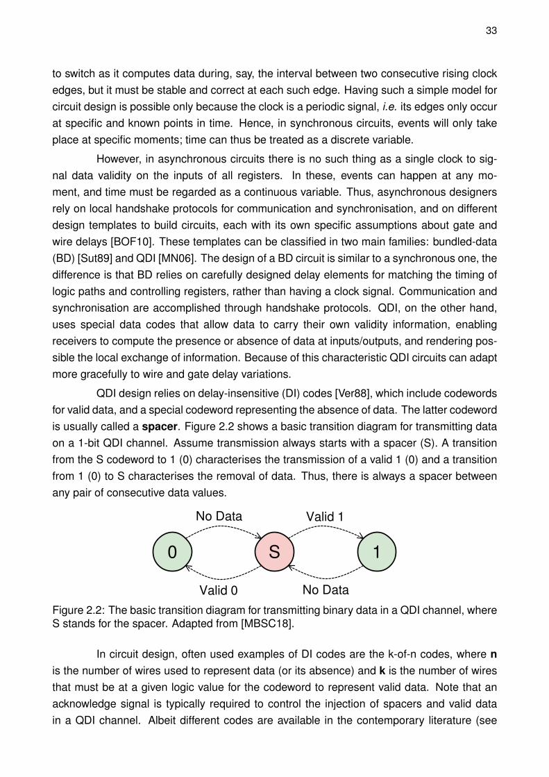
QDI design relies on delay-insensitive (DI) codes [Ver88], which include codewordsfor valid data, and a special codeword representing the absence of data. The latter codewordis usually called a spacer. Figure 2.2 shows a basic transition diagram for transmitting dataon a 1-bit QDI channel. Assume transmission always starts with a spacer (S). A transitionfrom the S codeword to 1 (0) characterises the transmission of a valid 1 (0) and a transitionfrom 1 (0) to S characterises the removal of data. Thus, there is always a spacer betweenany pair of consecutive data values.
S0 1
Valid 1
Valid 0
No Data
No Data
Figure 2.2: The basic transition diagram for transmitting binary data in a QDI channel, whereS stands for the spacer. Adapted from [MBSC18].
In circuit design, often used examples of DI codes are the k-of-n codes, where nis the number of wires used to represent data (or its absence) and k is the number of wiresthat must be at a given logic value for the codeword to represent valid data. Note that anacknowledge signal is typically required to control the injection of spacers and valid datain a QDI channel. Albeit different codes are available in the contemporary literature (see
34
e.g. [Ver88]), according to Martin and Nyström [MN06], the most practical class of DI codesis the 1-of-n (or one-hot), and more specifically the 1-of-2 code. The latter is the basis toform codes to represent any n-bit information using two wires to denote each of the n bits,producing the so-called dual-rail code. Besides data encoding QDI design usually impliesa choice of either a 2-phase or a 4-phase communication protocol [MN06]. The majority ofQDI designs available in the state-of-the-art, from networks-on-chip [BCV+05, PMMC10], togeneral purpose processors [MNW03], and network switches [DLD+14] primarily rely on a 4-phase protocol and dual-rail or 1-of-4 codes. This work focus attention on 4-phase, dual-railQDI design.
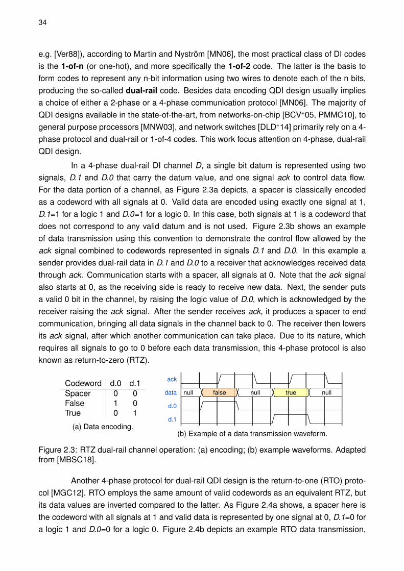
In a 4-phase dual-rail DI channel D, a single bit datum is represented using twosignals, D.1 and D.0 that carry the datum value, and one signal ack to control data flow.For the data portion of a channel, as Figure 2.3a depicts, a spacer is classically encodedas a codeword with all signals at 0. Valid data are encoded using exactly one signal at 1,D.1=1 for a logic 1 and D.0=1 for a logic 0. In this case, both signals at 1 is a codeword thatdoes not correspond to any valid datum and is not used. Figure 2.3b shows an exampleof data transmission using this convention to demonstrate the control flow allowed by theack signal combined to codewords represented in signals D.1 and D.0. In this example asender provides dual-rail data in D.1 and D.0 to a receiver that acknowledges received datathrough ack. Communication starts with a spacer, all signals at 0. Note that the ack signalalso starts at 0, as the receiving side is ready to receive new data. Next, the sender putsa valid 0 bit in the channel, by raising the logic value of D.0, which is acknowledged by thereceiver raising the ack signal. After the sender receives ack, it produces a spacer to endcommunication, bringing all data signals in the channel back to 0. The receiver then lowersits ack signal, after which another communication can take place. Due to its nature, whichrequires all signals to go to 0 before each data transmission, this 4-phase protocol is alsoknown as return-to-zero (RTZ).
Codeword d.0 d.1Spacer 0 0False 1 0True 0 1
(a) Data encoding.
ack
data null false null true null
d.0
d.1
(b) Example of a data transmission waveform.
Figure 2.3: RTZ dual-rail channel operation: (a) encoding; (b) example waveforms. Adaptedfrom [MBSC18].
Another 4-phase protocol for dual-rail QDI design is the return-to-one (RTO) proto-col [MGC12]. RTO employs the same amount of valid codewords as an equivalent RTZ, butits data values are inverted compared to the latter. As Figure 2.4a shows, a spacer here isthe codeword with all signals at 1 and valid data is represented by one signal at 0, D.1=0 fora logic 1 and D.0=0 for a logic 0. Figure 2.4b depicts an example RTO data transmission,

35
which starts with all signals at 1 in the data channel. As soon as the sender puts valid datain the channel, the receiver may acknowledge it by lowering ack. Next, all data signals mustreturn to 1 to denote a spacer, ending transmission. When the spacer is detected by thereceiver, it raises the ack signal and new data can follow. The idea behind the RTO protocolis simple but powerful and allows a better design space exploration for QDI circuits, enablingoptimisations in power [MGC12] and robustness [MGHC14]. Furthermore, as demonstratedin [MPC14], RTZ and RTO can be mixed in a same QDI design and the conversion of val-ues between them requires only an inverter per wire. According to Martin and Nyström, in[MN06], such conversion is DI and does not compromise the robust functionality of a QDIcircuit. This article refers to signals operating under the RTZ (RTO) protocol as RTZ (RTO)signals.
Codeword d.0 d.1Spacer 1 1False 0 1True 1 0
(a) Data encoding.
ack
data null false null true null
d.0
d.1
(b) Example of a data transmission waveform.
Figure 2.4: RTO dual-rail channel operation: (a) encoding; (b) example waveforms. Adaptedfrom [MBSC18].
2.4 Static Timing Analysis
Timing analysis is an important step in digital circuit design, since establishing thecircuit performance under certain operating conditions is often one of the main project re-quirements. Historically timing is analysed using electrical simulation, this is called DynamicTiming Analysis (DTA). It relies on stimulating every possible path of electrical-level modelof the circuit being tested and measuring the time elapsed until a stable output is given.However, this type of analysis is computationally expensive and relies on a good source ofstimuli to cover every possible path.
Alternatively, Static Timing Analysis (STA) provides a cheaper alternative to analysingthe timing of the circuit globally through simulation. It relies on delay models of small com-ponents of the circuit, e.g. logic gates. These delays models are used to estimate the delayof every possible timing path in the circuit. This avoids the coverage problem and is lesscomputational intensive, allowing the use of STA on much larger circuits.
The delay models of components are created using electrical simulation in a pro-cess called characterisation. A delay model of a component captures characteristics of arcs.An arc is a timing path internal to a component, it captures how changes in a input affects

36
the circuit. There are three types of arcs: (i) hidden arcs, where a change in input doesnot affect any output; (ii) transition arcs, where a change in input causes a transition in theoutput; and (iii) constraint arcs, which are limitations of when an input can change. As anexample, the propagation arcs of an OR gate are shown in Figure 2.5a. Each dashed linerepresent two propagation arcs, one for the rise and another for the fall of the output Z .
A possible model is the non-linear delay model (NLDM), which is composed oftables that capture characteristics for each arc based on the input slew and output capac-itance. Some characteristics captured by the NLDM tables are: (i) slew rate, the time anoutput takes to finish transitioning once it starts; (ii) propagation delay, the time a transitionin an input propagates to the output ; (iii) power consumption, the energy consumed by atransition in the arc. The delay model of a component also captures the capacitance of pins.
The timing paths are acyclic with well defined start and end points. A timing pathis composed by a chain of arcs. Transitions propagate in these paths thru arcs, due tothis characteristic a timing path is also called a propagation path throughout this work.Figure 2.5b shows a circuit implementing a XOR gate using two inverters and three NANDgates. The timing arc relating the fall of the output Z when the input A rises is highlighted. Arise transition in A activates an arc of g0 which produce a fall transition in its output, in turnthis transition activates an arc of "g2" that causes a rise in its output, which finally activatean arc of g4 that cause a fall transition in the primary output Z .
A
BZ
(a) Timing arcs internal to anOR gate.
g2
g3
g0
g1
g4
B
A
Z
10
1
1
(b) Timing path of a multi-gate XOR circuit.
Figure 2.5: Timing models used by the STA engine: (a) gate timing arcs; (b) timing paths.
From the information contained in the delay model, it is possible to analyse thetiming paths of circuits. The STA engine computes the delay of the timing paths with thefollowing sequence of steps: First the capacitance of each net is computed based on thecomponents connected to it, the capacitance of primary outputs are provided as a param-eter. The STA engine then creates an acyclic directed graph containing all possible timingpaths in the circuit from the circuit netlist and propagation arcs. For each arc in the graph,the STA engine uses the slew information in the delay model to compute the slew rate ofevery possible transition, the slew of the primary inputs are provided as a parameter. Once

37
the capacitance and slew rate are computed, the STA engine is able to use the propagationarcs of the delay models to compute the time each transition occurs in the timing path.
On synchronous sequential circuits, the timing paths are bounded by clock events.The start point of each path is either a primary input or the output of a clocked sequentialelement. Also, the end point is either an primary output or the input of a clocked sequentialelement.
The clock provides a periodic time reference which can be used to compute thetiming of the circuit. Primary inputs are assumed to be synchronous to clock events andsequential elements produce new values on clock events. This implies that a clock eventtriggers a sequence of transitions in propagation paths. The time between the first and thelast transition in the propagation path is called its propagation delay of that path.
A more comprehensive background on STA lays beyond the scope of this Disser-tation. The interested reader may consult works like that of Harris “Skew-Tolerant CircuitDesign” [Har01].

38
39
3. THE PSEUDO-SYNCHRONOUS SDDS-NCL DESIGN TEMPLATE
The timing of propagation paths in a digital circuit can be computed using STA.Commercial EDA tools attempt to find and optimal solution that respects the timing budgetwhile balancing power and area consumption. Also, during physical implementation, STAenables an optimal placement of gates in the layout, guaranteeing that wire delays do notcompromise the circuit functionality. On synchronous flop-based circuits, the clock periodbounds the delay of propagation paths between two registers. The last transition in eachpath must occur a certain time prior to the clock edge for the circuit to work correctly.
The pseudo-synchronous flow enables us to define a pseudo-clock period, analo-gous to a clock period of a synchronous flop-based circuit. This pseudo-clock can then beused to constrain the delay of propagation paths between two registers. The SDDS-NCLdesign template leverages standard EDA to synthesise and optimise combinational QDI cir-cuits. This Chapter introduces the Pseudo-Synchronous SDDS-NCL, a QDI template thatcombines and extends both SDDC-NCL and the Pseudo-Synchronous flows. This enablesthe synthesis and optimisation of sequential asynchronous circuits with constrained propa-gation paths using commercial EDA tools.
3.1 The SDDS-NCL Asynchronous Design Template (Related Work)
NCL is an asynchronous design template to construct QDI circuits – Nowick andSingh present a good summary of this and other templates in [NS15a, NS15b]. Fant andBrandt proposed NCL in [FB96], targeting RTZ 1-of-n schemes. It was the technology usedfor industrial designs produced by Theseus Logic in the late 90s. Since then, NCL hasbeen explored by different research groups and employed for different applications, typicallyfocusing on low power and robust design [JSL+10, CCGC10, SCH+11, ZSD10, GLY10]. NCLassumes a semi-custom design method, and relies on a basic set of components designedat the cell level, called NCL gates. As Fant and Brandt discuss in [FB96], these gatesallow the construction of logic blocks that ensure the completeness of input criterion, whichenforces that a logic block only produces a spacer (valid data) in its outputs when all its inputshave a spacer (valid data). The authors state that this is the key to ensure DI operation.
NCL gates are often called threshold gates, but this is imprecise, because they donot exactly implement threshold logic functions (TLFs) as defined, e.g. in [Hur69]. Rather,these gates implement modifications of such TLFs coupled to specific mechanisms to ensurethe completeness of input criterion [FB96]. Before defining TLFs, a useful concept is that ofunate functions [BSVMH84], as all TLFs are unate [Hur69]:

40
Definition 3.1.1 A Boolean function f (x1, x2, ..., xn) is said to be positive unate in xi (1 ≤ i ≤n), if ∀xj , i 6= j , f (x1, ... , xi−1, 1, ... , xn) ≥ f (x1, ... , xi−1, 0, ... , xn). Similarly, f is called negativeunate in xi if ∀xj , i 6= j , f (x1, ... , xi−1, 0, ... , xn) ≥ f (x1, ... , xi−1, 1, xi+1, ..., xn). If a function isneither positive unate nor negative unate in xi , it is said to be binate in xi . Moreover, if afunction is positive or negative unate in all its variables it is called a unate function. A unatefunction that is positive (negative) unate in all its variables is called a positive (negative)unate function. Also, this dissertation calls positive (negative) unate gates those thatimplement positive (negative) unate functions.
Definition 3.1.2 An n-variable threshold logic function (TLF) τ is an n-variable unatefunction defined by a threshold value T ∈ N∗ and weights wi ∈ N∗ assigned to eachof its variables xi such that:
τ =
1,
n−1∑i=0
wixi ≥ T
0,n−1∑i=0
wixi < T(3.1)
Hurst [Hur69] defines threshold gates with the threshold and weights being realnumbers. This work restricts attention to non-zero, natural threshold and weights. TLFs canbe either negative or positive unate in a given input – but not binate. However, to ensure thecompleteness of input criterion, NCL gates must be positive unate in all their inputs, as theytarget RTZ templates, where data validity is given by wires at 1. The OFF-set of a logic gateis the set of input patterns that force its output to 0. Analogously, the ON-set is the set ofinput patterns that force the output of a logic gate to 1. Because the spacer corresponds toall wires at 0, the OFF-set of an NCL gate includes just the condition where all inputs are 0.
As Fant and Brandt discuss in [FB96], while a QDI logic block is transitioning be-tween a spacer and valid data, output values of the block should be either a spacer or validdata. Therefore, NCL gates must also account for situations where an input combination isneither in the ON-set nor in the OFF-set. In these no gate output should transition. Thisleads to the definition of the correct behaviour for NCL gates.
Definition 3.1.3 An n-input NCL gate is a logic gate with a threshold value T ∈ N∗, a weightwi ∈ N∗ assigned to each variable xi (i = 1, ... , n), and a hysteresis mechanism such that thegate output Q at each instant of time t is given by:
Qt =
1,n∑
i=1wixi ≥ T
0,n∑
i=1xi = 0
Qt−1, 0 <n∑
i=1wixi < T
(3.2)
Figure 3.1a shows a generic NCL gate symbol, where n is the number of inputs ofthe gate and T is the threshold of the TLF it implements, for which each input has a weight

41
wi . If a weight wi is omitted, wi = 1 is assumed. Weights come after the W specifier. As anexample, Figure 3.1b shows the symbol of a 3-input NCL gate with threshold 3 and weights2, 1 and 1 (in the order from the topmost input down). Figure 3.1c shows the truth table forthis latter example, computed from Equation (3.2). Accordingly, the output of the gate onlyswitches to 0 when all inputs are at 0. Also, because x1 has weight 2, x2 and x3 have weight1 and the threshold is 3, the gate only switches to 1 when x1 is at 1 and at least one of theother inputs is at 1. In all other cases the output remains unchanged.
TWw0..wn-1
x0
xn-1
... Q
(a) NCL gate, generic.
3W211
x0
Qx1
x2
(b) Specific NCL gate.
X0 X1 X2 Qt
0 0 0 00 0 1 Qt−1
0 1 0 Qt−1
0 1 1 Qt−1
1 0 0 Qt−1
1 0 1 11 1 0 11 1 1 1
(c) 3W211 gate truth table.
Figure 3.1: Characteristics of NCL gates: (a) generic symbol; (a) generic symbol; (b) specificsymbol example; (c) example truth table behaviour.
It is possible to build classic Boolean logic blocks with NCL gates, as Figure 3.2illustrates. This schematic shows a generate path circuit fragment for an RTZ dual-railKogge-Stone adder, taken from [MTMC14]. Note that this circuit only generates a spaceroutput when all dual-rail inputs (Gi , Pi , Gp) have spacers. Recalling Figure 3.1, the output ofan NCL gate only goes to 0 when all its inputs are at 0, which means that gates G0-G3 inFigure 3.2 only write a 0 in their outputs when all primary inputs have spacers. Also notethat the outputs become valid data only when all inputs display valid data. Accordingly, n0 is1 only if Pi and Gp are valid 1s (i.e. Pi .1 = 1 and Gp.1 = 1) and n1 is 1 only if Pi has a valid0 and Gp has a valid 1, Pi has a valid 1 and Gp has a valid 0, or both Pi and Gp have a valid0. In this way, n0 and n1 are valid only if the primary inputs Pi and Gp are valid. Similarly,gates G2 and G3, which generate the outputs of the logic block, have their inputs connectedto n0, n1 and primary input Gi , and these gates only generate valid data when their inputsare valid.
Even though the classic definition of an NCL gate relies on TLFs for their ON-set,different works (e.g. [JN08, RST12]) report the usage of non-TLF positive unate functions.This work also considers such functions, but as exceptions to the definition. Since these donot agree with the given NCL gate definition, they are called hysteretic functions. Hystereticfunctions can be described using three minterm sets: (i) the ON-set contain all minterms that
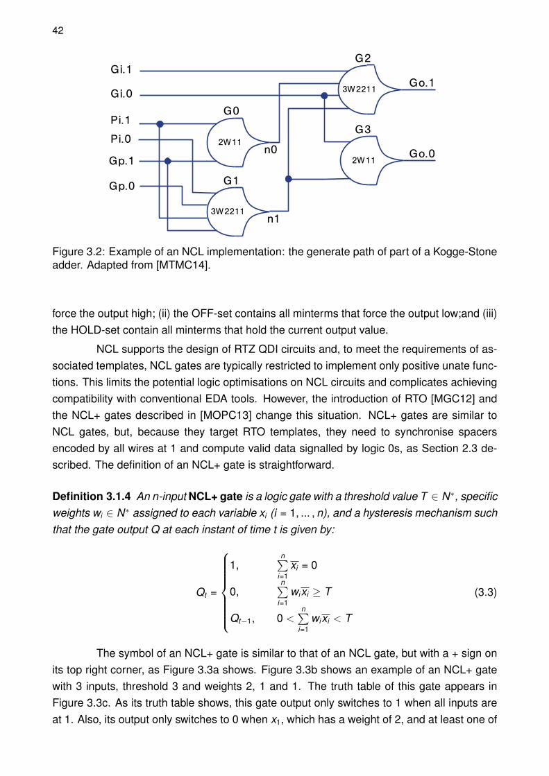
42
Gi.0
Gi.1
Pi.0
Pi.1
Gp.0
Gp.1
2W11
3W2211
3W2211
2W11
Go.1
Go.0n0
n1
G0
G3
G2
G1
Figure 3.2: Example of an NCL implementation: the generate path of part of a Kogge-Stoneadder. Adapted from [MTMC14].
force the output high; (ii) the OFF-set contains all minterms that force the output low;and (iii)the HOLD-set contain all minterms that hold the current output value.
NCL supports the design of RTZ QDI circuits and, to meet the requirements of as-sociated templates, NCL gates are typically restricted to implement only positive unate func-tions. This limits the potential logic optimisations on NCL circuits and complicates achievingcompatibility with conventional EDA tools. However, the introduction of RTO [MGC12] andthe NCL+ gates described in [MOPC13] change this situation. NCL+ gates are similar toNCL gates, but, because they target RTO templates, they need to synchronise spacersencoded by all wires at 1 and compute valid data signalled by logic 0s, as Section 2.3 de-scribed. The definition of an NCL+ gate is straightforward.
Definition 3.1.4 An n-input NCL+ gate is a logic gate with a threshold value T ∈ N∗, specificweights wi ∈ N∗ assigned to each variable xi (i = 1, ... , n), and a hysteresis mechanism suchthat the gate output Q at each instant of time t is given by:
Qt =
1,n∑
i=1xi = 0
0,n∑
i=1wixi ≥ T
Qt−1, 0 <n∑
i=1wixi < T
(3.3)
The symbol of an NCL+ gate is similar to that of an NCL gate, but with a + sign onits top right corner, as Figure 3.3a shows. Figure 3.3b shows an example of an NCL+ gatewith 3 inputs, threshold 3 and weights 2, 1 and 1. The truth table of this gate appears inFigure 3.3c. As its truth table shows, this gate output only switches to 1 when all inputs areat 1. Also, its output only switches to 0 when x1, which has a weight of 2, and at least one of

43
the other inputs, both with weight 1, are at 0. For all other combinations of inputs, the gatekeeps its output value. In these cases, the output only switches to 1 (0) when all inputs areat 1 (0).
TWw0..wn-1
x0
xn-1
... Q
(a) NCL+ gate, generic.
3W211
x0
Qx1
x2
(b) Specific NCL+ gate.
X0 X1 X2 Qt
0 0 0 00 0 1 00 1 0 00 1 1 Qt−1
1 0 0 Qt−1
1 0 1 Qt−1
1 1 0 Qt−1
1 1 1 1
(c) 3W211 gate truth table.
Figure 3.3: Characteristics of NCL+ gates: (a) generic symbol; (a) generic symbol; (b)specific symbol example; (c) example truth table behaviour.
As in NCL, NCL+ gates are also useful to build logic blocks. For instance, Fig-ure 3.4 shows the NCL+ version of the same generate path of the Kogge-Stone adder fromFigure 3.2. The circuit topology is exactly the same as that of the NCL version. In fact,the gate characteristics are the same. The only difference is that NCL+ gates replace NCLgates with the same number of inputs, thresholds and weights. Hence, all internal nodesand primary inputs and outputs follow the RTO protocol, instead of RTZ.
Gi.0
Gi.1
Pi.0
Pi.1
Gp.0
Gp.1
2W11
3W2211
3W2211
2W11
Go.1
Go.0n0
n1
G0
G3
G2
G1
Figure 3.4: Example of an NCL+ implementation: the generate path of part of a Kogge-Stoneadder. Adapted from [MTMC14].
The advent of NCL+ created the possibility of mixing NCL and NCL+ in a single cir-cuit, because RTO protocol signals can be translated to RTZ protocol signals and vice-versa

44
[MPC14]. Recalling Section 2.3, the conversion of a signal from RTO to RTZ, or the otherway around, only requires inverters, each of which implements a negative unate function.Thus, as discussed in [MTMC14], the mix of NCL and NCL+ enables the use of negativeunate functions, which allows further optimisation opportunities and expands the designspace of QDI circuits. For each positive unate NCL (NCL+) gate, a negative unate gate canbe defined, where the latter has its OFF-SET defined as the ON-SET of the former. To differ-entiate negative unate gates from positive unate ones from Definitions 3.1.3 and 3.1.4, theseare named Inverted NCL and NCL+ gates (or INCL and INCL+, respectively) and definedaccordingly.
Definition 3.1.5 An n-input INCL gate is a logic gate with a threshold value T ∈ N∗, specificweights wi ∈ N∗ (i = 1, ... , n), assigned to each variable xi and a hysteresis mechanism suchthat the gate output Q at each instant of time t is given by:
Qt =
1,n∑
i=1xi = 0
0,n∑
i=1wixi ≥ T
Qt−1, 0 <n∑
i=1wixi < T
(3.4)
Definition 3.1.6 An n-input INCL+ gate is a logic gate with a threshold value T ∈ N∗, spe-cific weights wi ∈ N∗ (i = 1, ... , n), assigned to each variable xi and a hysteresis mechanismsuch that the gate output Q at each instant of time t is given by:
Qt =
1,n∑
i=1wixi ≥ T
0,n∑
i=1xi = 0
Qt−1, 0 <n∑
i=1wixi < T
(3.5)
From a functional point of view, the only difference between an NCL (NCL+) and anINCL (INCL+) gate is that their ON- and OFF-sets are swapped. However, they all still rely ona hysteresis behaviour to ensure the respect of QDI properties. To produce INCL/INCL+ gatesymbols, a bubble is added to the output of the respective non-inverted gate symbol. Usinginverted gates it is possible to convert signals from RTZ to RTO, and vice versa. Becauseeach time an inverted gate is used the protocol changes (including the codeword to rep-resenting spacers), circuits using (I)NCL and (I)NCL+ gates are called spatially distributeddual spacer NCL (or SDDS-NCL) [MTMC14].
Figure 3.5 shows an example of SDDS-NCL circuit equivalent to the ones in Fig-ures 3.2 and 3.4. As the figure shows, when the circuit inputs present spacers, it issues aspacer in its output. In this figure, all INCL gates have 1 in their outputs, which means that
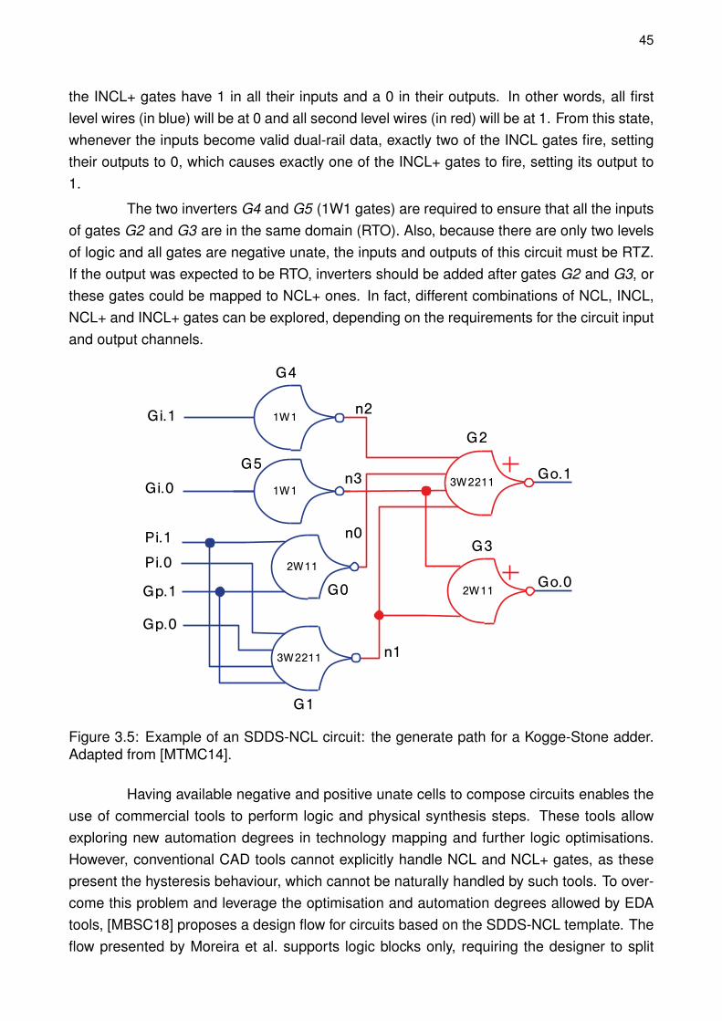
45
the INCL+ gates have 1 in all their inputs and a 0 in their outputs. In other words, all firstlevel wires (in blue) will be at 0 and all second level wires (in red) will be at 1. From this state,whenever the inputs become valid dual-rail data, exactly two of the INCL gates fire, settingtheir outputs to 0, which causes exactly one of the INCL+ gates to fire, setting its output to1.
The two inverters G4 and G5 (1W1 gates) are required to ensure that all the inputsof gates G2 and G3 are in the same domain (RTO). Also, because there are only two levelsof logic and all gates are negative unate, the inputs and outputs of this circuit must be RTZ.If the output was expected to be RTO, inverters should be added after gates G2 and G3, orthese gates could be mapped to NCL+ ones. In fact, different combinations of NCL, INCL,NCL+ and INCL+ gates can be explored, depending on the requirements for the circuit inputand output channels.
Gi.0
Gi.1
Pi.0
Pi.1
Gp.0
Gp.1
2W11
3W2211
3W2211Go.1
Go.0
1W1
2W11
1W1
n0
n1
G0
G3
G2
G1
n3
n2
G5
G4
Figure 3.5: Example of an SDDS-NCL circuit: the generate path for a Kogge-Stone adder.Adapted from [MTMC14].
Having available negative and positive unate cells to compose circuits enables theuse of commercial tools to perform logic and physical synthesis steps. These tools allowexploring new automation degrees in technology mapping and further logic optimisations.However, conventional CAD tools cannot explicitly handle NCL and NCL+ gates, as thesepresent the hysteresis behaviour, which cannot be naturally handled by such tools. To over-come this problem and leverage the optimisation and automation degrees allowed by EDAtools, [MBSC18] proposes a design flow for circuits based on the SDDS-NCL template. Theflow presented by Moreira et al. supports logic blocks only, requiring the designer to split
46
sequential from combinational blocks and synthesise the latter in isolation. This Chapterlater further extends the SDDS-NCL and the pseudo-synchronous [TBV12] design flows tosupport the fully automated synthesis of both combinational and sequential blocks.
The SDDS-NCL design flow comprises two steps: logic and physical synthesis.Both are based in the usage of virtual libraries, a concept similar to that of image librariesproposed for the Proteus asynchronous design flow [BDL11]. The virtual library (VL) conceptbuilds upon the definition of virtual function (VF), presented herein.
Definition 3.1.7 A virtual function (VF) is an n-input Boolean function associated with ann-input NCL, NCL+, INCL or INCL+ gate, called its support gate. The truth table of a virtualfunction f is defined as follows:
1. if the support gate of f is an NCL gate θ, the ON-set of f is the same as the ON-set ofθ. The OFF-set of f comprises all other n-input patterns;
2. if the support gate of f is an NCL+ gate φ, the OFF-set of f is the same as the OFF-setof φ. The ON-set of f comprises all other n-input patterns;
3. if the support gate of f is an INCL gate ψ, the OFF-set of f is the same as the OFF-setof ψ. The ON-set of f comprises all other n-input patterns;
4. if the support gate of f is an INCL+ gate υ, the ON-set of f is the same as the ON-setof υ. The OFF-set of f comprises all other n-input patterns.
If the support gate of f is of types NCL or NCL+, f is a positive VF. Otherwise, f is a negativeVF.
Note that each VF always has exactly one NCL and one NCL+ support gates orone INCL and one INCL+ support gates. Reference [MNM+14] provides the detailed de-scription of a method to compute the support gates for VFs. As another consequence ofDefinition 3.1.7, all positive VFs are positive unate functions, but not all positive unate func-tions are positive VFs. Furthermore, all negative VFs are negative unate functions, but notall negative unate functions are negative VFs. Hence, all VFs are unate functions, but notall unate functions are VFs. As an example, consider the 3-input NCL gate 3W211 depictedin Figure 3.1. The reader can verify that the virtual function f1 for this gate can be expressedby f1 = x0.(x1 + x2). Another example is the 3-input NCL+ gate 3W211 depicted in Figure 3.3has a virtual function f2 expressible by f2 = x0 + x1.x2. As expected and can be verified, theseVFs are positive unate.
Definition 3.1.8 A virtual library (VL) is a library of cells such that their functions are mod-elled exclusively using VFs. In this way, it is guaranteed that synthesis tools will be able tohandle a VL, as all VFs are unate functions. Two types of VLs exist, NCL VLs and NCL+VLs.
47
1. An NCL VL is a VL composed exclusively by NCL and INCL gates modelled using VFs.
2. An NCL+ VL is a VL composed exclusively by NCL+ and INCL+ gates modelled usingVFs.
3.2 Pseudo-Synchronous Weak-Conditioned Half Buffer (Related Work)
Weak-Conditioned Half Buffer or WCHB is a classical asynchronous QDI templateused to build sequential asynchronous circuits [BOF10]. It assumes the use of a DI code(often, the dual-rail one) and allows constructing asynchronous pipelines where stages con-taining data are surrounded by stages containing spacers and vice-versa (originating thehalf buffer denomination, meaning a data token at each two stages).
In [TBV12] Thonnart et al. compare the timing arcs of a resetable C-element, abasic building block of WCHB pipeline registers, to those of edge-triggered flip-flops, abasic building block of synchronous pipelines. From this analysis arises the proposal ofpseudo-synchronous WCHB design technique, which relies on a clever modelling of asyn-chronous components and on standard static timing analysis (STA) tools to optimise se-quential logic specifically for the WCHB QDI design template. They propose a modified,pseudo-synchronous (flop-like) model to represent resetable C-elements, building timing ta-bles in the Open Liberty standard supported by conventional STA tools. The underlyingreasoning is that conventional tools can analyse timing paths that start and end only atflip-flops, primary inputs, or primary outputs.
The Thonnart et al. model allows the analysis of paths that start and/or end inpseudo-synchronous flops without adding significant error to the actual delay of these C-elements. This work also details the specification of a pseudo-clock that guides the synthesisdecision making process and constrains each logic stage during synthesis. Included is alsoa methodology to characterise pseudo-synchronous C-elements.
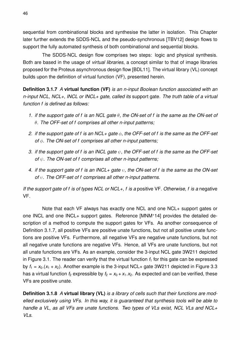
The original timing arcs of a C-element appear in Figure 3.6a, arcs from A, B toZ, and the arc from Reset to Z. These arcs are modelled as a function of the slew from anincoming transition in an input pin and the capacitance being driven by the output pin. In themodel devised for use in the pseudo-synchronous flow, the arcs are modified to mimic thoseequivalent to a flip-flop (as in Figure 3.6b) [TBV12].
Here, the C-element Reset is transformed into a pseudo-clock pin and each of itsoriginal propagation arcs are split in two parts: (i) a clock propagation delay (in green),from Reset to Z (a function of the slew in Reset and of the capacitance in Z); and (ii) setupconstraints (in blue), from A to Reset (a function of the slew in A and of the slew in Reset)and from B to Reset (a function of the slew in B and of the slew in Reset). Note that, sincethe sequential nature of the Reset pin is only a mechanism to create the pseudo-clock, its
48
A
B
Reset
Z
(a) Propagation arcs extracted from a con-ventional description.
A
B
Reset
Z
(b) Propagation arcs from a pseudo-synchronous description.
Figure 3.6: Two arc models for a resetable C-element: (a) conventional description; (b)pseudo-synchronous description [TBV12].
slew is usually ignored. This way, the generated delay tables are a single row (or column)that depends only on the slew of A or B and on the capacitance driven by Z.
The reasoning behind this is that the original arcs can be constructed from the sumof a clock propagation delay and from a setup constraint of the Thonnart et al. model. Forexample, the original A to Z arc is represented by the propagation delay from Reset to Zadded to the setup constraint from A to Reset.
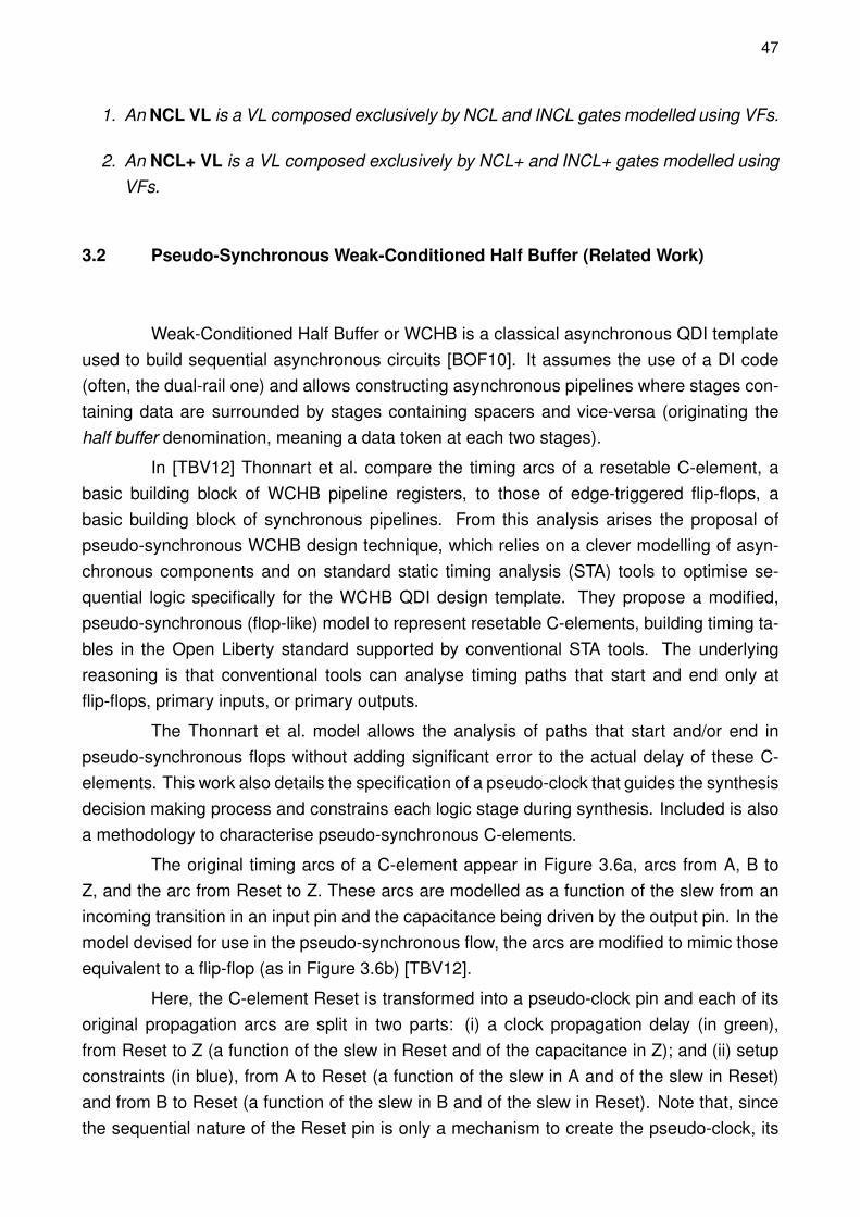
This way, every time the STA tool encounters a pseudo-synchronous flop model ofa C-element, it identifies a new start point for paths that begin at output Z and a new endpoint for paths finishing at inputs A or B. This is crucial to enable STA in WCHB pipelines,as every pipeline stage is marked by the presence of a group of C-elements (e.g. 2 for a1-of-2, 4-phase encoding, 1-bit data channel). The logic paths between these C-elementsare optimised to meet the defined period (say λ) of the pseudo-clock connected to the Resetpin.
For example, Figure 3.7 shows how these paths are analysed in a WCHB pipeline.It shows a single C-element composing the memory of each pipeline stage (hardly true inpractice, due to the use of DI codes) and two types of logic paths: (i) the forward logic(usually where useful computation happens); and (ii) the backward logic (usually used forflow control). As the Figure shows, between every pair of C-elements in a cycle there areforward and backward logic paths that are constrained by a single pseudo-clock, with periodλ, entering at the Reset pin (not shown). Furthermore, there are also paths between theinput channel and the first C-element and the last C-element and the output channel.
One of the major drawbacks of the Thonnart et al. method is that it can cause errorswhen computing delays for the C-elements, as a result of the regeneration of the original arcfrom the sum of the two new arcs. This takes place because the new arcs do not measurethe delay of the cell as an explicit function of the slew in its inputs and the capacitance in its
49
Forward Logic
Backward Logic
Backward Logic
Forward Logic
C
Backward Logic
Forward Logic
C C
Figure 3.7: Simplified view of a 1-bit data channel WCHB pipeline, showing the inner cyclescontrolled by the pseudo-clock.
output. It rather builds two independent delay values that are then added, one as a functionof the capacitance driven by Z and another as a function of the slew in A or B.
Another drawback is that the reset network is tied to a (pseudo-)clock networkand optimising these signals independently becomes challenging, since balancing of resetsignals conflicts with the tool trying to synthesise a clock tree for the pseudo-clock. Also,the annotation of delays for post-implementation simulations in this model is tricky. Thecreated arcs will be in accordance to the pseudo-synchronous model, not fitting the originalC-element arcs, and will not reflect the real delay of the circuit. Thonnart et al. suggest thatthe original models be provided to the tool for delay annotation. However, this causes theinsertion of loop breakers, which complicates analysis.
To deal with these issues, this work proposes creating a fictitious clock pin (G) andtwo new models for characterising resetable C-elements, as Figure 3.8 details: the pseudo-flop model (Figure 3.8a), used during synthesis; and the pseudo-latch model (Figure 3.8b)that preserves all original propagation arcs and is only used to extract delay annotations forpost-synthesis simulation. The fictitious pin G allows preserving the original Reset pin timingarcs. This enables using STA to design a reset network, meeting the constraints extractedfrom the cell characterisation process.
The pseudo-latch model relies on the fundamental behaviour of latches. A latchis a sequential element that has two distinctive operation modes, transparent and opaque.During the transparent mode operation, a latch has a direct arc from its data input to itsdata output and during the opaque mode it holds data. Transitions between these modesare governed by a clock signal, which imposes sequential arcs on the latch. Therefore, alatch timing model typically includes a setup constraint and a clock to output delay (as inflip-flops), and a combinational arc from its input to its output (to serve in those cases whenthe latch is transparent). This model respectively creates valid start and end points for STAat the outputs and inputs of latches. During the pseudo-latch characterisation, this feature isleveraged to preserve the original arcs of the C-element, while avoiding the insertion of loopbreakers. In simulation, it is enough that the behavioural model consider the cell as alwaysin transparent mode to reflect these delays, ignoring any sequential arc.

50
A
B
Reset
Z
G
(a) Proposed pseudo-flop model.
A
B
Reset
Z
G
(b) Proposed pseudo-latch model.
Figure 3.8: Proposed characterisation models for a resetable C-element with a dummy clockpin, G: (a) pseudo-flop; (2) pseudo-latch.
Although this work only explores the use of pseudo-synchronous C-elements withreset, the use of a fictitious pin for the pseudo-clock allows any NCL(NCL+) gate to becharacterised both using pseudo-flop or pseudo-latch models. Gates characterised usingthis technique can be modelled as sequential combo cells, composed of a combinationalgate with the virtual function (VF) of the original gate followed by the sequential element.This allows EDA tools to differentiate pseudo-flop functions during synthesis.
3.3 The Pseudo-Synchronous SDDS-NCL Synthesis Flow
The SDDS-NCL combinational synthesis flow, originally proposed in [Mor16] wassignificantly extended and modified to produce the SDDS-NCL sequential synthesis flow. Yetthe flow described in this Section bears some resemblance to the original one. For example,the use of commercial tools also produces netlists that do not correspond to the intendedbehaviour of the final circuit (the X-Netlists). As in the original combinational flow, these canbe corrected by using a low complexity Fix X-Netlist procedure, but the new flow uses a quitedistinct approach to implement this procedure, and it is used in more places in the flow.
Figure 3.9 depicts the pipeline structure for a sequential SDDS-NCL circuit. Bothforward (in green) and backward (in blue) propagation logic modules are SDDS-NCL. Reg-isters are pseudo-synchronous resetable C-elements. Forward-propagation logic is alwayspositive unate, meaning it preserves the logic protocol of the inputs. Conversely, backward-propagation (completion detection) logic is negative unate, meaning that it inverts the proto-col of its inputs. Hence, sequential elements have their inputs at opposite protocol domains.

51
C
CForwardLogic
(SDDS-NCL)
C
C
CompletionDetection
(SDDS-NCL)
CompletionDetection
(SDDS-NCL)
ForwardLogic
(SDDS-NCL)
C
C
CompletionDetection
(SDDS-NCL)
Figure 3.9: Structure of a sequential SDDS-NCL pipeline.
Figure 3.10 depicts the pseudo-synchronous SDDS-NCL synthesis flow. The flowis substantiated as a set of TCL scripts driving tools of the Cadence™EDA framework. Logicsynthesis and optimisation employ Genus™ 18.1. Placement and routing are achieved withInnovus™ 18.1.
The flow takes a pre-expanded dual-rail netlist as input. The process of dual-railexpansion, part of the Pulsar flow, is addressed in Section 5.4. The dual-rail input netlist con-tains both combinational and sequential elements. Pseudo-flops are explicitly instantiatedas sequential elements in pipeline stages. Boolean expressions are used to describe the be-haviour of combinational logic as VFs for both forward and backward propagation betweensequential elements.
SDDS-NCL requires that the logic modules be strictly unate, meaning that all inputsof a gate must reside on the same domain. Since SDDS-NCL is only used for combinationallogic, there is no problem in having sequential gates with their inputs at different domains.To solve this, a “size_only” constraint is set on all sequential elements to preserve their logicfunction.
Genus synthesises and optimises the combinational logic in both backward andforward propagation paths. Synthesis and optimisation must meet some requirements togenerate a fixable X-Netlist: (i) they must not generate intermediate circuits with binatefunctions, as gates in these circuits have inputs at different domains (RTZ and RTO), whichwould break the circuit behaviour; (ii) they must not produce circuits with gate inputs tied to aconstant, as a constant at gate inputs may inhibit the set or reset behaviour of NCL (NCL+)gates.
In the new design flow the input always implements unate functions, all internalnodes should be unate in path start points, i.e. primary inputs and register outputs. However,according to Das et al. [DCB93] it is possible that the synthesis tool to perform a binaterealisation of a unate input function. To overcome this issue Moreira [Mor16] proposed usingdesign for testability (DFT) techniques, guaranteeing that requirement (i) above is alwaysmeet. Requirement (ii) is fulfilled setting “iopt_force_constant_removal=true” on Genus.
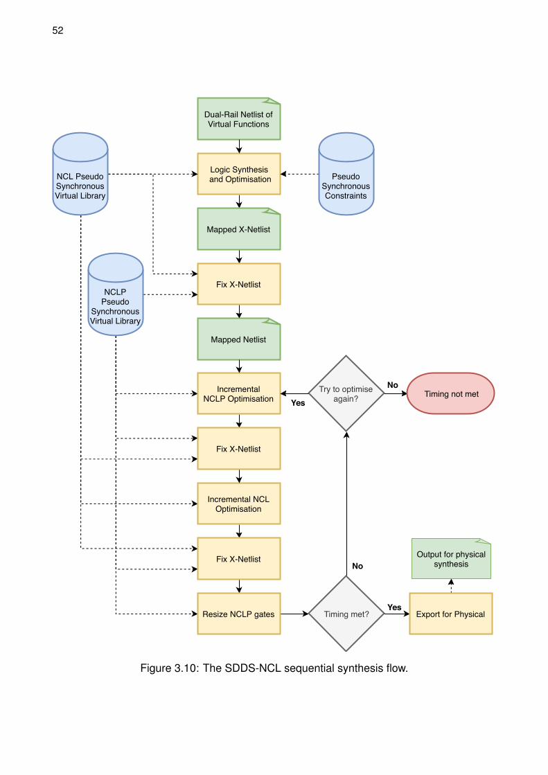
52
No
Try to optimiseagain?
Dual-Rail Netlist ofVirtual Functions
Logic Synthesis and Optimisation
Mapped X-Netlist
Fix X-Netlist
NCL PseudoSynchronousVirtual Library
NCLPPseudo
SynchronousVirtual Library
Mapped Netlist
PseudoSynchronousConstraints
IncrementalNCLP Optimisation
Incremental NCLOptimisation
Fix X-Netlist
Resize NCLP gates Timing met?Yes
Export for Physical
YesTiming not met
No
Fix X-Netlist
Output for physicalsynthesis
Figure 3.10: The SDDS-NCL sequential synthesis flow.

53
Assuming the initial circuit description is NCL (i.e. an RTZ description), the outputof sequential gates are guaranteed to be RTZ, since initial synthesis and optimisation stepspreserve this characteristic. It is also safe to assume from this condition that all primaryinputs are also RTZ.
To produce a circuit with the correct behaviour, gates which are in the RTO domainmust be NCL+ and gates in the RTZ domain must be NCL. The combinational logic in bothforward and backward propagation paths are processed by Algorithm 3.1, which identifiesthe protocol of each gate and employs the correct gate type.
In the Fix X-Netlist algorithm, a gate is considered in RTZ if its non-inverting fan-insare RTZ and its inverting fan-ins are RTO. Conversely, a gate is considered in RTO if itsnon-inverting fan-ins are RTO and its inverting fan-ins are RTZ. Figure 3.11 illustrates this.
3
RTZ RTO
2
41
3
RTZ RTO
2
41
5
5
6
6
Figure 3.11: Illustration of the RTO and RTZ gate classification process.
If a combinational gate is classified as both RTO and RTZ, the X-Netlist is deemedunsuitable for correction and the synthesis is invalid. The only gates allowed to be in bothRTO and RTZ domains are the registers, but these do not need to be processed by the FixX-Netlist algorithm.
The initial netlist correction may result in a circuit that no longer meets the designconstraints. In this case, further optimisation steps are needed to meet them. These optimi-sation steps are run on each set of gates independently, to avoid undoing the initial netlistcorrection. After optimising a set of gates, the Fix X-Netlist correction algorithm is re-run tocorrect any domain changes introduced by the optimisation. These steps are iteratively rununtil the timing constraints are fulfilled.

54
Require: Mapped X-NetlistEnsure: Fixed SDDS-NCL Netlist
{Breath first gate classification}Add all primary inputs to rtz set;Add all registers to rtz set;while exist unexplored gates in the X-Netlist do
for g in rtz doif g is inverting gate then
Add combinational fanout of g to the rto set;else
Add combinational fanout of g to the rtz set;end if
end forfor g in rto do
if g is inverting gate thenAdd combinational fanout of g to the rtz set;
elseAdd combinational fanout of g to the rto set;
end ifend for
end while
{Correct gates in RTZ}for g in rtz do
if g is NCL+ thenReplace g with NCL gate of same vFunction;
end ifend for
{Correct gates in RTO}for g in rto do
if g is NCL thenReplace g with NCL+ gate of same vFunction;
end ifend for
Algorithm 3.1: The Fix X-Netlist algorithm.

55
After logic synthesis, optimisation and correction steps, the final netlist can beplaced and routed by a physical synthesis tool. However, meeting timing constraints duringphysical synthesis may require some additional optimisation steps. If the logic is changedduring these steps, logical correctness of the circuit may be compromised.
Prior to place and route, NCL+ gates are marked with “dont_touch” and “dont_use”,NCL gates are marked “size_only” and buffers are left free for the physical synthesis tool touse. This guarantees the logic will not suffer any changes during physical synthesis andgives the physical synthesis tool freedom to place buffers and resize gates to meet timing.

56
57
4. A NEW MODEL FOR CYCLE TIME COMPUTATION
The throughput of asynchronous circuits is not directly dictated by its slowest prop-agation path. It is rather defined as the inverse of the system cycle time, i.e. the meantime between two results. The cycle time depends on complex interactions between multi-ple pipeline stages and the involved delays. The definition of (asynchronous) cycle time isexplored in Section 4.1.
Analysis of the cycle time is also not straightforward. It requires complex modelsthat capture the interactions internal to asynchronous circuits. Section 4.2 reviews the full-buffer channel network (FBCN) timing model and Section 4.3 extends this model to supporthalf-buffer pipelines. These models can be used in conjunction with STA to compute themaximum cycle time of an asynchronous circuit. This is further explored in Section 4.4,where we present a methodology based on linear programming to compute the maximumcycle time of circuits modelled using both FBCN and HBCN.
By the end of this chapter it is expected that the reader is provided with a methodol-ogy to analyse the maximum cycle time of asynchronous circuits using global timing modelsand traditional STA techniques. Thus, estimating the minimal throughput of the circuit duringits design.
4.1 Cycle Time of Asynchronous Circuits
According to Beerel, Ozdag, Ferretti [BOF10] the cycle time of an asynchronouscircuit is the time between two consecutive computation results. On a synchronous circuitthis is dictated by the clock period, i.e. a synchronous circuit (most often) produces a resultevery clock cycle. However, for asynchronous circuits this is defined as the time betweentwo consecutive tokens.
The cycle time is limited by the internal delays and token placement in the circuit. Itis best observed under an ideal null-delay environment, i.e. an environment that consumestokens as soon as they arrive and produces new tokens as soon as the previous is acknowl-edged. This ideal of null-delay environment is used here to isolate the circuit from externalinfluences and data dependent delay variations. Another reason for using an ideal environ-ment model is that the cycle time is observed when the pipeline is at full capacity. When thepipeline is empty or partially empty, the time between results at the output is not dependenton internal factors only, but also on the availability of tokens coming from the environmentand propagating in the pipeline.
Also, the cycle times observed in an asynchronous circuit can present data depen-dent variations. The data flow within the asynchronous system may be data dependent,

58
because they may present choice behaviour due to characteristics such as arbitration, splitsand merges. Systems with such behaviour are called non-deterministic. On such systems,the tokens propagate through different paths with different delays, thus affecting the cycletime.
Furthermore, even deterministic systems, which present no data-dependent tokenflow, can show variations in the cycle time observed at inputs or outputs. For instance,the delays of an individual pipeline stage can be data dependent, e.g. an adder unit maycomplete faster if all inputs are zero. This can lead to situations that a token advances fasterthrough the pipeline, arriving earlier at the output, but leaving part of the pipeline idle waitingfor data from a slower part. This idle waiting time will appear as an increase in the cycle timeof the output for the next token. Also, temporarily faster delays near the input may accepttokens into the pipeline faster than they can be processed by later pipeline stages. Thiscan cause tokens to queue up in the pipeline entrance. This queuing causes a delay to theadmission of the next token, which translates as increases in the observed cycle time in theinput.
On average, these variations may cancel each other, i.e. a token with a faster cycletime can be followed by a token with a slower cycle time. The observed cycle time forms adistribution around the average cycle time. On a system that generates an output for eachinput, the observed average cycle time must be the same on the system inputs and outputs.This average cycle time is the system cycle time, i.e. disregarding transient variations, onaverage the pipeline is capable of producing new results after each cycle time has elapsed.
To demonstrate this effect, the observed cycle time of the input and output of 6-stage multiply and accumulate (MAC) unit is shown in Figure 4.1. The measurements wereextracted using delay annotated post-synthesis simulation and a zero-delay external envi-ronment to produce and consume data.
The circuit presents a wider cycle time distribution at the output, indicating thatsometimes the pipelines stages near the output (namely the accumulator) complete fasterthan the multiplier (at the beginning of the pipe) is capable of providing new data.
4.2 The FBCN Timing Model (Related Work)
Beerel, Ozdag, Ferretti [BOF10] proposed in their book the Full-Buffer channelnetwork (FBCN), a timed marked graph model that captures the behaviour of full-bufferasynchronous pipelines. FBCN allows modelling the global timing of an asynchronous circuitfrom individual circuit timing paths (extractable using STA tools).

59
2.7 2.8 2.9 3.0 3.1Cycle Time (ns)
Dens
ityOutputInputMean
Figure 4.1: Observed cycle time distribution at the input and output of an integer, 6-stage,multiply-and-accumulate circuit.
The formal definition in [BOF10] derives from a comprehensive Petri net definition.However, since FBCN is a marked graph, it is possible to use the definition in Section 2.1.3to formally redefine FBCN as follows:
Definition 4.2.1 (Full-Buffer Channel Network - FBCN) A Full-Buffer Channel Network isdefined as the 3-tuple N = (T , C, I0), where T is a set of transitions, C = {(u, v ) : u, v ∈T , u 6= v} is a set of channels, and I0 : C 7→ {ack , req} is a function defining each channelinitial state.
An FBCN is equivalently represented as a marked graph defined as the 3-tupleN = (T , P, M0), where T is a set of transitions; P = {(u, v ) : u, v ∈ T} is a set of places andM0 is a set of initially marked places. The equivalence between N and G is defined by thefollowing set of rules:
∀(u, v ) ∈ P : ∃{(u, v ), (v , u)} ⊆ P (4.1)
∀(u, v )|I0((u, v )) = ack ,∃(v , u) ∈ M0 (4.2)
∀(u, v )|I0((u, v )) = req,∃(u, v ) ∈ M0 (4.3)
Equation 4.1 states that every channel is represented by a pair of places, a forwardpropagation place and a backward propagation place; Equation 4.2 states that the channel
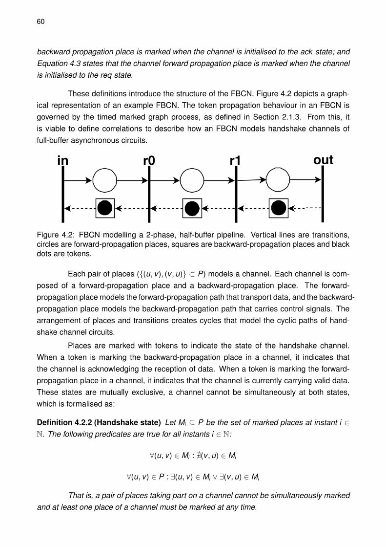
60
backward propagation place is marked when the channel is initialised to the ack state; andEquation 4.3 states that the channel forward propagation place is marked when the channelis initialised to the req state.
These definitions introduce the structure of the FBCN. Figure 4.2 depicts a graph-ical representation of an example FBCN. The token propagation behaviour in an FBCN isgoverned by the timed marked graph process, as defined in Section 2.1.3. From this, itis viable to define correlations to describe how an FBCN models handshake channels offull-buffer asynchronous circuits.
r1 r0 in out
Figure 4.2: FBCN modelling a 2-phase, half-buffer pipeline. Vertical lines are transitions,circles are forward-propagation places, squares are backward-propagation places and blackdots are tokens.
Each pair of places ({(u, v ), (v , u)} ⊂ P) models a channel. Each channel is com-posed of a forward-propagation place and a backward-propagation place. The forward-propagation place models the forward-propagation path that transport data, and the backward-propagation place models the backward-propagation path that carries control signals. Thearrangement of places and transitions creates cycles that model the cyclic paths of hand-shake channel circuits.
Places are marked with tokens to indicate the state of the handshake channel.When a token is marking the backward-propagation place in a channel, it indicates thatthe channel is acknowledging the reception of data. When a token is marking the forward-propagation place in a channel, it indicates that the channel is currently carrying valid data.These states are mutually exclusive, a channel cannot be simultaneously at both states,which is formalised as:
Definition 4.2.2 (Handshake state) Let Mi ⊆ P be the set of marked places at instant i ∈N. The following predicates are true for all instants i ∈ N:
∀(u, v ) ∈ Mi : @(v , u) ∈ Mi
∀(u, v ) ∈ P : ∃(u, v ) ∈ Mi ∨ ∃(v , u) ∈ Mi
That is, a pair of places taking part on a channel cannot be simultaneously markedand at least one place of a channel must be marked at any time.

61
Transitions capture the handshaking behaviour of registers or of the environment.A transition fires when all of its inbound places are holding tokens, that is, it synchronises theacknowledgement from the outbound channel with the data from the inbound channel pro-ducing an acknowledgement in the inbound channel and propagating data to the outboundchannel. This effectively models the behaviour of a 2-phase handshake protocol.
Each place is annotated with the delay from the propagation path it represents.This delay can be extracted from the circuit using STA tools. For instance, assuming a 2-phase bundled-data design, the place indicating the forward propagation place in a channelis annotated with the propagation delay of the request signal on that channel. Conversely,the backward propagation place is annotated with the delay of the acknowledge signal onthe channel.
4.3 The HBCN Timing Model
As the name states, an FBCN is a model suitable to describe full-buffer pipelines.In a full-buffer pipeline there are only valid data being propagated and acknowledged. Eachchannel in some FBCN can be in one of two states, either acknowledging or transmittingvalid data.
Conversely, in half-buffer pipelines valid data tokens are always followed by spacertokens. Spacer tokens are characteristic of half-buffer circuits such as WCHB pipelines.They need to be represented in the model to correctly capture the behaviour of a half-bufferpipeline. In a half-buffer pipeline each channel can be in one of four states: propagatingdata, acknowledging data, propagating a spacer and acknowledging a spacer.
Since FBCN is not capable of modelling this behaviour naturally, this work proposesthe Half Buffer Channel Network (HBCN), a modification of FBCN to explicitly model half-buffer pipelines. HBCNs are also timed marked graphs, and all properties of FBCN regardingcycle time analysis hold true for them. An HBCN models the behaviour of 4-phase half-bufferpipelines, by representing the four possible states of each half-buffer channel. These statesare captured using four places per channel. A pair of transitions is required at each end ofa channel to synchronise the propagation of valid data and spacers. The structure of theHBCN can be formalised as follows.
Definition 4.3.1 (HBCN) A Half-Buffer Channel Network (HBCN) is defined by the 4-tupleN = (T , Γ, C, I0), where T is a set of transitions, Γ = {(t , t ′) : t , t ′ ∈ T , t 6= t ′} is a setof transition pairs, C = {(u, v ) : u, v ∈ Γ, u 6= v} is a set of channels, and I0 : C 7→{acknull , reqdata, ackdata, reqnull} is a function defining each channel initial state. An HBCNhas a characteristic marked graph defined as the 3-tuple G = (T , P, M0) where T is a the setof transitions of the HBCN, P = {(u, v ) : u, v ∈ T} is a set of places, and M0 ⊂ P is a set

62
of initially marked places. The relation between N and G is defined by the following set ofrules:
(u, v ) ∈ Γ =⇒ u, v ∈ T (4.4)
((u, u′), (v , v ′)) ∈ C =⇒ {(u, v ), (u′, v ′), (v ′, u), (v , u′)} ⊆ P (4.5)
I0(((u, u′), (v , v ′))) = acknull =⇒ (v ′, u) ∈ M0 (4.6)
I0(((u, u′), (v , v ′))) = reqdata =⇒ (u, v ) ∈ M0 (4.7)
I0(((u, u′), (v , v ′))) = ackdata =⇒ (v , u′) ∈ M0 (4.8)
I0(((u, u′), (v , v ′))) = reqnull =⇒ (u′, v ′) ∈ M0 (4.9)
Implication 4.4 states that every transition taking part on a transition pair must existon the transition set; Implication 4.5 states that each channel is expanded to four places,two forward propagation places (for data and spacer) and two cross-connected backwardpropagation places; Implications 4.6 to 4.9 define which places are initially marked to setchannels to their respective initial states.
A possible intuition to understand the HBCN model is to see it as two parallelFBCNs cross-connected by the backward propagation places at each channel. One net-work captures the propagation of spacers and the other valid data. The handshake protocolis captured by cross-connecting the null backward propagation place of a stage to the datatransition of the previous stage and by connecting the data back-propagation place to theprevious stage null transition. This enforces that data propagation depends on the propaga-tion of spacers and vice-versa.
Delays can be attributed to each place of the HBCN to capture the propagationtime of data and spacers in the network. This allows using HBCN to analyse the timingcharacteristics of a half-buffer pipelines. The cycle time is defined as the time a token takesto return to a place after being removed, that is, the time it takes for a channel to transitionsto between all its states back to its initial state.
To illustrate concepts an example HBCN is now derived from the Weak-ConditionedHalf Buffer (WCHB) pipeline in Figure 4.3. This WCHB is a simple Quasi-Delay Insensitive(QDI) half-buffer pipeline template that employs Delay Insensitive (DI) codes, completiondetectors and a 4-phase RTZ handshake protocol. C-elements are used as registers tolatch DI codes in each stage. This example uses a 1-of-2 code, thus requiring 2 C-elements(one for each rail), the employed completion detector is a NOR gate. A spacer is representedby having the two rails at zero and valid data is represented by having one of the rails at one.
The example circuit comprises two registers (r0 and r1), one input (in) and oneoutput (out). There are 3 channels in this circuit: (i) from the input to r0; (ii) from r0 to r1;and (iii) from r1 to the output. For each channel, the forward propagation path is the pairof rails transporting data and spacers, and the backward propagation place is the comple-
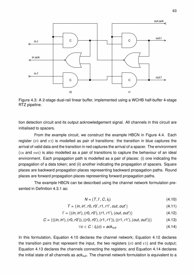
63
C
C
C
C
in.f
in.t
in.ack
out.f
out.t
out.ack
r0 r1
Figure 4.3: A 2-stage dual-rail linear buffer, implemented using a WCHB half-buffer 4-stageRTZ pipeline.
tion detection circuit and its output acknowledgement signal. All channels in this circuit areinitialised to spacers.
From the example circuit, we construct the example HBCN in Figure 4.4. Eachregister (r0 and r1) is modelled as pair of transitions: the transition in blue captures thearrival of valid data and the transition in red captures the arrival of a spacer. The environment(in and out) is also modelled as a pair of transitions to capture the behaviour of an idealenvironment. Each propagation path is modelled as a pair of places: (i) one indicating thepropagation of a data token; and (ii) another indicating the propagation of spacers. Squareplaces are backward propagation places representing backward propagation paths. Roundplaces are forward propagation places representing forward propagation paths.
The example HBCN can be described using the channel network formulation pre-sented in Definition 4.3.1 as:
N = (T , Γ, C, I0) (4.10)
T = {in, in′, r0, r0′, r1, r1′, out , out ′} (4.11)
Γ = {(in, in′), (r0, r0′), (r1, r1′), (out , out ′)} (4.12)
C = {((in, in′), (r0, r0′)), ((r0, r0′), (r1, r1′)), ((r1, r1′), (out , out ′))} (4.13)
∀c ∈ C : I0(c) = acknull (4.14)
In this formulation, Equation 4.10 declares the channel network; Equation 4.12 declaresthe transition pairs that represent the input, the two registers (r0 and r1) and the output;Equation 4.13 declares the channels connecting the registers; and Equation 4.14 declaresthe initial state of all channels as acknull . The channel network formulation is equivalent to a
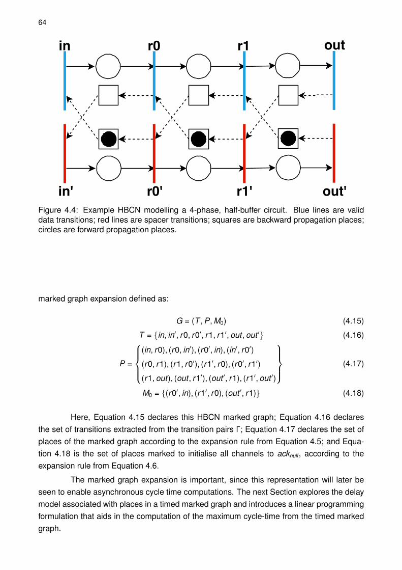
64
r1
r1'
r0
r0'
in
in'
out
out'Figure 4.4: Example HBCN modelling a 4-phase, half-buffer circuit. Blue lines are validdata transitions; red lines are spacer transitions; squares are backward propagation places;circles are forward propagation places.
marked graph expansion defined as:
G = (T , P, M0) (4.15)
T = {in, in′, r0, r0′, r1, r1′, out , out ′} (4.16)
P =
(in, r0), (r0, in′), (r0′, in), (in′, r0′)
(r0, r1), (r1, r0′), (r1′, r0), (r0′, r1′)
(r1, out), (out , r1′), (out ′, r1), (r1′, out ′)
(4.17)
M0 = {(r0′, in), (r1′, r0), (out ′, r1)} (4.18)
Here, Equation 4.15 declares this HBCN marked graph; Equation 4.16 declaresthe set of transitions extracted from the transition pairs Γ; Equation 4.17 declares the set ofplaces of the marked graph according to the expansion rule from Equation 4.5; and Equa-tion 4.18 is the set of places marked to initialise all channels to acknull , according to theexpansion rule from Equation 4.6.
The marked graph expansion is important, since this representation will later beseen to enable asynchronous cycle time computations. The next Section explores the delaymodel associated with places in a timed marked graph and introduces a linear programmingformulation that aids in the computation of the maximum cycle-time from the timed markedgraph.
65
4.4 Calculating the Maximum Cycle Time
Both HBCN and FBCN are timed marked graphs that contain cycles. Cycles aredefined as a cyclic sequence of places where tokens repeatedly flow. On a timed markedgraph, token propagation is ruled by the place delays. On these models, the cycle time isdefined as the sum of the delays of places taking part in a cycle divided by the number oftokens residing in the cycle.
The maximum cycle time is the largest cycle time in the graph. Ultimately, due tocomplex interactions in the circuit, this largest cycle time dominates the overall asynchronouspipeline performance. Determining the maximum cycle time is important to analyse pipelineperformance.
The maximum cycle time is an upper limit for the circuit cycle time. This is animportant performance measurement, as it bounds circuit performance floor. On a markedgraph model (such as the HBCN) the maximum cycle time is defined as the greatest cycletime in the circuit. This value is not always intuitively found, especially on large markedgraphs with multiple interacting cycles such as the HBCN of a large circuit.
Magott [Mag84] has devised a methodology using linear programming to computethe maximum cycle time in a Petri net. It works by estimating the time each transition firesbased on a system of constraints.
The time a transition fires is called the transition arrival time. A transition arrivaltime is limited by its incoming places. The transition can only fire after all of its incomingplaces allows it. A place only allows its outgoing transition to fire after it has been holding atoken for the duration of its delay.
Any place receives a token after its incoming transition fires. If a place holds atoken at the initial time it is assumed that it has received that token at the previous cycletime. From these statements it is possible to formalise an arrival time constraint for eachplace.
Definition 4.4.1 (Arrival time constraint) Inequation 4.19 is the arrival time constraint de-fined for a place p = (u, v ), where au is the arrival time for the incoming transition u; av is thearrival time for the outgoing transition v; dp ≥ 0 is the delay associated with place p; m0(p)is the number of initial tokens in p (1, if initially marked, else 0); and φ ≥ 0 is the cycle timeof the marked graph.
av ≥ au + dp −m0(p)φ (4.19)
Inequation 4.19 states that v fires dp time units after u has fired, unless p is initiallymarked, than it is assumed that v has fired one cycle before.

66
Since the delay attributed to each place is the maximum delay of the propagationpath, it is safe to assume that the transition will fire as soon as all arrival constraints aresatisfied. Following this assumption, the maximum cycle-time is the minimal value of φthat satisfies the set of constraints. This can be computed using a linear programming (LP)solver, by providing the arrival time constraints with the place delays and setting the objectivefunction as minimising φ.
The LP solver solution returns values for each variable in the input formulation. Thisincludes the value of φ, which is the maximum cycle time. But it also includes values for thearrival time of each transition, byproduct values with no concrete meaning, one solution ofmany possible ones. The LP solver is free to attribute values to these variables, only thedistance and ordering of these values are important to the solution process.
However, more useful information could be extracted from the solution. For in-stance, the free slack is the amount of time a token stays in a place after its delay has expired.This information is useful for optimising the pipeline performance. Beerel et al. [BLDK06] hasextended the arrival time constraint formulation to extract the free slack of each place, cre-ating the arrival time equation.
Definition 4.4.2 (Arrival Time Equation) Equation 4.20 is the arrival time equation definedfor each place p = (u, v ), where au is the arrival time for the incoming transition u; av is thearrival time for the outgoing transition v; dp ≥ 0 is the delay associated with place p; ρp ≥ 0is the free slack of place p, m0(p) is the number of initial tokens in p (1 if initially marked,else 0); and φ ≥ 0 is the cycle time of the marked graph.
av = au + dp + ρp −m0(p)φ (4.20)
The arrival time equation can replace the arrival time constraint in the LP solverformulation. The solution of the augmented formulation yields the maximum cycle time, thearbitrary transition arrival times and the free slack of each place.
An example to demonstrate this methodology is to compute the maximum cycletime of a 3-stage circular half-buffer circuit. The example circuit is modelled as an HBCN,depicted in Figure 4.5, with the formulation below.

67
N = (Γ, C, I0) (4.21)
Γ = {r0, r1, r2} (4.22)
C = {(r0, r1), (r1, r2), (r2, r0)} (4.23)
I0(c) =
reqdata c = (r0, r1)
acknull c = (r1, r2)
reqnull c = (r2, r0)
(4.24)
r0
r0'
r2'
r1 r2
r1'
Figure 4.5: HBCN of a 3-stage, circular half-buffer circuit.
Using Definition 4.3.1 it is possible to find the HBCN equivalent marked graph,which is as follows.
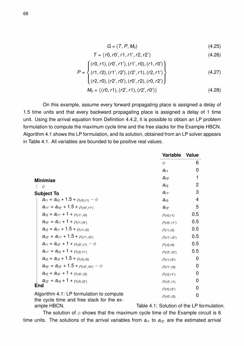
68
G = (T , P, M0) (4.25)
T = {r0, r0′, r1, r1′, r2, r2′} (4.26)
P =
(r0, r1), (r0′, r1′), (r1′, r0), (r1, r0′)
(r1, r2), (r1′, r2′), (r2′, r1), (r2, r1′)
(r2, r0), (r2′, r0′), (r0′, r2), (r0, r2′)
(4.27)
M0 = {(r0, r1), (r2′, r1), (r2′, r0′)} (4.28)
On this example, assume every forward propagating place is assigned a delay of1.5 time units and that every backward propagating place is assigned a delay of 1 timeunit. Using the arrival equation from Definition 4.4.2, it is possible to obtain an LP problemformulation to compute the maximum cycle time and the free slacks for the Example HBCN.Algorithm 4.1 shows the LP formulation, and its solution, obtained from an LP solver appearsin Table 4.1. All variables are bounded to be positive real values.
Minimiseφ
Subject Toar1 = ar0 + 1.5 + ρ(r0,r1) − φar1′ = ar0′ + 1.5 + ρ(r0′,r1′)
ar0 = ar1′ + 1 + ρ(r1′,r0)
ar0′ = ar1 + 1 + ρ(r1,r0′)
ar2 = ar1 + 1.5 + ρ(r1,r2)
ar2′ = ar1′ + 1.5 + ρ(r1′,r2′)
ar1 = ar2′ + 1 + ρ(r2′,r1) − φar1′ = ar2 + 1 + ρ(r2,r1′)
ar0 = ar2 + 1.5 + ρ(r2,r0)
ar0′ = ar2′ + 1.5 + ρ(r2′,r0′) − φar2 = ar0′ + 1 + ρ(r0′,r2)
ar2′ = ar0 + 1 + ρ(r0,r2′)End
Algorithm 4.1: LP formulation to computethe cycle time and free slack for the ex-ample HBCN.
Variable Valueφ 6ar1 0ar0′ 1ar2 2ar1′ 3ar0 4ar2′ 5ρ(r0,r1) 0.5ρ(r0′,r1′) 0.5ρ(r1,r2) 0.5ρ(r1′,r2′) 0.5ρ(r2,r0) 0.5ρ(r2′,r0′) 0.5ρ(r1,r0′) 0ρ(r1′,r0) 0ρ(r2,r1′) 0ρ(r2′,r1) 0ρ(r0,r2′) 0ρ(r0′,r2) 0
Table 4.1: Solution of the LP formulation.The solution of φ shows that the maximum cycle time of the Example circuit is 6
time units. The solutions of the arrival variables from ar1 to ar2′ are the estimated arrival

69
times, they show the order in which transitions happen in a cycle. The solution of variablesρ(r0,r1) to ρ(r2′,r0′) show that the forward propagation places have a free slack of 0.5 time units,which means that data transitioning in that path have to wait 0.5 time units to propagateafter they are ready. The solution of variables ρ(r1,r0′) to ρ(r0′,r2) indicates that the backwardpropagation paths are part of the critical cycle, data propagating in these paths evolve to thenext stage as soon as they arrive to their registers. The existence of free slack in this circuitshows that the pipeline is not optimised.
4.5 Constraining the Maximum Cycle Time
The last Section proposed and explored a technique to analyse the cycle time ofHBCNs. However, this technique assumes a pre-synthesised circuit. This Section extendsthe linear programming (LP) formulations used for cycle time analysis to derive the individualpath delays that satisfy a target cycle time.
Commercial EDA tools heavily rely on Static Timing Analysis (STA). Tools that per-form STA are timing driven, they operate with the concept of a timing budget to guide theirsynthesis effort. For a circuit to work correctly, the timing of the combinational logic in thesepaths must be less or equal to their timing budget. Logic synthesis tools employ STA toelaborate logic circuits that respect the defined timing budget. Usually, for synchronousflop-based circuits, the timing budget is constrained using the target clock period, but timingexceptions can also be set to constrain individual paths. Chapter 3 introduced the pseudo-synchronous SDDS-NCL, a novel QDI design template that enables commercial EDA toolsto synthesise and optimise sequential QDI circuits with constrained propagation paths. Thepseudo-synchronous SDDS-NCL template allows defining a pseudo-clock and some timingexceptions to constraint the delay of individual propagation paths.
The previous Section developments relied on annotating an HBCN model with de-lays of individual propagation paths. From such HBCN it was then possible to derive asystem of arrival equations av = au + dp + ρp − m0(p)φ. These were then used in an LPformulation to compute the maximum cycle time of the circuit modelled by the HBCN. Recallthat dp is the place delay corresponding to a timing path and φ is the maximum cycle time.
The cycle time analysis method is now extended to a synthetic approach. Insteadof analysing the maximum cycle time of a given circuit, the HBCN and arrival equation areused to compute the delay constraints of places required to meet a desired maximum cycletime (φ). For that, a single delay λ is assigned to every place corresponding to timing pathswhich are to be constrained. A system of arrival time equations is then extracted from theHBCN model, the maximum cycle time value φ is set to the desired value and the valueof λ is maximised using an LP solver. The computed value of λ is the pseudo-clock usedto constrain the timing paths of the original circuit. The intuition behind this method is to

70
discover “how slow” the constrained timing paths can be, without violating the maximumcycle time constraint. Since the pseudo-synchronous SDDS-NCL template allows defininga pseudo-clock to constrain the delay of individual paths, it is fair to assume that the delayof these paths will be limited by λ.
Notice that the method proposed here allows the designer to optionally specify afixed delay for any place p by attributing a numeric value to dp. This is useful when a timingpath has a known delay or is its delay is fine-tuned by the designer using timing exceptions.These fixed delays are taken in consideration during the pseudo-clock computation, thusguaranteeing that the pseudo-clock constraint still bounds the maximum cycle time. Theuse of fixed delays on timing paths known to be fast in the critical cycle may allow thepseudo-clock constraint to be more relaxed.
To demonstrate the method, consider an example of constraining the 3-stage cir-cular buffer whose HBCN appears in Figure 4.5, to the maximum cycle time of 2 ns. In thisexample, assume that the places corresponding to the channel connecting the transition pair(r0, r0′) to (r1, r1′) have a fixed delay of 100 ps. The LP formulation used to compute thepseudo-clock constraint λ is depicted in Algorithm 4.2. It states that the value of λ shouldbe maximised, subject to φ = 2 and the system of arrival equations. Each arrival equationcorresponds to a place p = (u, v ) in the HBCN. These equations state that the transition onthe postset of a place should occur at least λ time units after the transition on the preset ofthe same place, except on places with tokens where the transition can occur φ time unitsahead. Here, the free slack ρp is a positive real value that captures the amount of time atoken has to wait idling in a place after its propagation delay. Running this model on an LPsolver results in the solutions for the variables presented in Table 4.2.

71
Maximiseλ
Subject Toφ = 2ar1 = ar0 + 0.1 + ρ(r0,r1) − φar1′ = ar0′ + 0.1 + ρ(r0′,r1′)
ar0 = ar1′ + 0.1 + ρ(r1′,r0)
ar0′ = ar1 + 0.1 + ρ(r1,r0′)
ar2 = ar1 + λ + ρ(r1,r2)
ar2′ = ar1′ + λ + ρ(r1′,r2′)
ar1 = ar2′ + λ + ρ(r2′,r1) − φar1′ = ar2 + λ + ρ(r2,r1′)
ar0 = ar2 + λ + ρ(r2,r0)
ar0′ = ar2′ + λ + ρ(r2′,r0′) − φar2 = ar0′ + λ + ρ(r0′,r2)
ar2′ = ar0 + λ + ρ(r0,r2′)End
Algorithm 4.2: LP formulation to constrainthe cycle time of the HBCN in Figure 4.5to 2ns, using the pseudo-clock methodwith fixed delays.
Variable Valueλ 0.45 nsar1 0 nsar0′ 0.1 nsar2 0.55 nsar1′ 1 nsar0 1.1 nsar2′ 1.55 nsρ(r0,r1) 0.8 nsρ(r0′,r1′) 0.8 nsρ(r1,r2) 0.1 nsρ(r1′,r2′) 0.1 nsρ(r2,r0) 0.1 nsρ(r2′,r0′) 0.1 nsρ(r1,r0′) 0 nsρ(r1′,r0) 0 nsρ(r2,r1′) 0 nsρ(r2′,r1) 0 nsρ(r0,r2′) 0 nsρ(r0′,r2) 0 ns
Table 4.2: Solutions to the LP problem inAlgorithm 4.2
In this example, the fixed delays take part on the critical cycle and helped relaxingthe pseudo-clock constraint. To understand their impact, the experiment is repeated withoutfixing any place delays. Here, every timing path is equally constrained with the pseudo-clock value. The LP formulation is depicted in Algorithm 4.3 and its solution is presented inTable 4.3. Notice that value of λ is much lower in comparison. Note also the free slack isequally distributed along all forward-propagating places.
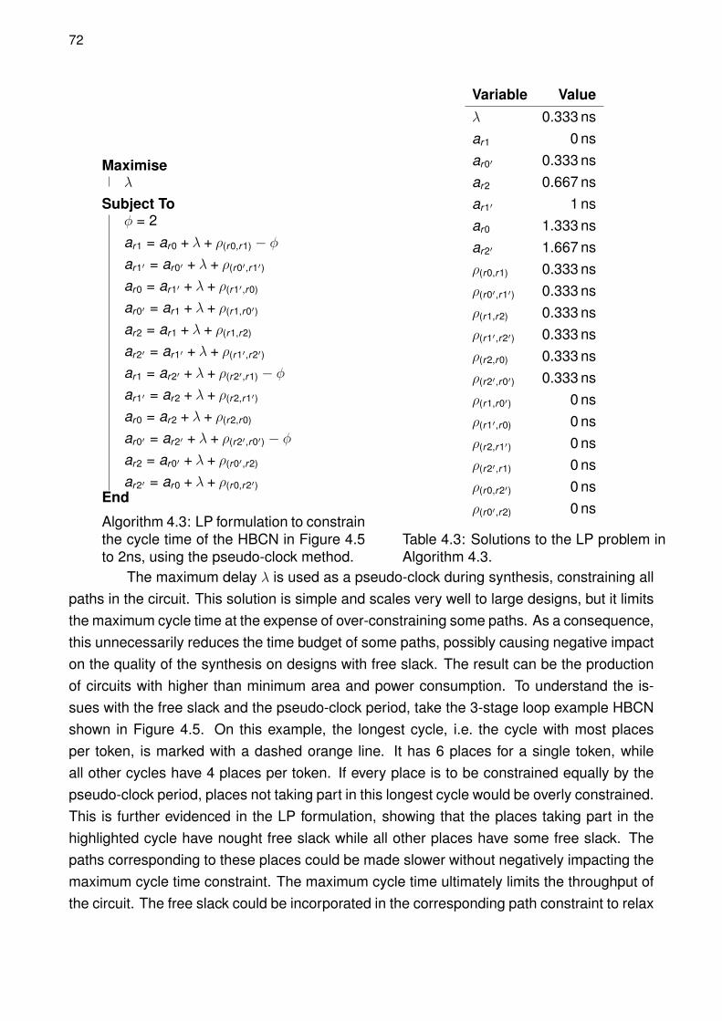
72
Maximiseλ
Subject Toφ = 2ar1 = ar0 + λ + ρ(r0,r1) − φar1′ = ar0′ + λ + ρ(r0′,r1′)
ar0 = ar1′ + λ + ρ(r1′,r0)
ar0′ = ar1 + λ + ρ(r1,r0′)
ar2 = ar1 + λ + ρ(r1,r2)
ar2′ = ar1′ + λ + ρ(r1′,r2′)
ar1 = ar2′ + λ + ρ(r2′,r1) − φar1′ = ar2 + λ + ρ(r2,r1′)
ar0 = ar2 + λ + ρ(r2,r0)
ar0′ = ar2′ + λ + ρ(r2′,r0′) − φar2 = ar0′ + λ + ρ(r0′,r2)
ar2′ = ar0 + λ + ρ(r0,r2′)End
Algorithm 4.3: LP formulation to constrainthe cycle time of the HBCN in Figure 4.5to 2ns, using the pseudo-clock method.
Variable Valueλ 0.333 nsar1 0 nsar0′ 0.333 nsar2 0.667 nsar1′ 1 nsar0 1.333 nsar2′ 1.667 nsρ(r0,r1) 0.333 nsρ(r0′,r1′) 0.333 nsρ(r1,r2) 0.333 nsρ(r1′,r2′) 0.333 nsρ(r2,r0) 0.333 nsρ(r2′,r0′) 0.333 nsρ(r1,r0′) 0 nsρ(r1′,r0) 0 nsρ(r2,r1′) 0 nsρ(r2′,r1) 0 nsρ(r0,r2′) 0 nsρ(r0′,r2) 0 ns
Table 4.3: Solutions to the LP problem inAlgorithm 4.3.
The maximum delay λ is used as a pseudo-clock during synthesis, constraining allpaths in the circuit. This solution is simple and scales very well to large designs, but it limitsthe maximum cycle time at the expense of over-constraining some paths. As a consequence,this unnecessarily reduces the time budget of some paths, possibly causing negative impacton the quality of the synthesis on designs with free slack. The result can be the productionof circuits with higher than minimum area and power consumption. To understand the is-sues with the free slack and the pseudo-clock period, take the 3-stage loop example HBCNshown in Figure 4.5. On this example, the longest cycle, i.e. the cycle with most placesper token, is marked with a dashed orange line. It has 6 places for a single token, whileall other cycles have 4 places per token. If every place is to be constrained equally by thepseudo-clock period, places not taking part in this longest cycle would be overly constrained.This is further evidenced in the LP formulation, showing that the places taking part in thehighlighted cycle have nought free slack while all other places have some free slack. Thepaths corresponding to these places could be made slower without negatively impacting themaximum cycle time constraint. The maximum cycle time ultimately limits the throughput ofthe circuit. The free slack could be incorporated in the corresponding path constraint to relax

73
the synthesis of these paths without affecting the cycle time. This could be solved by settingtiming exceptions on these paths.

74
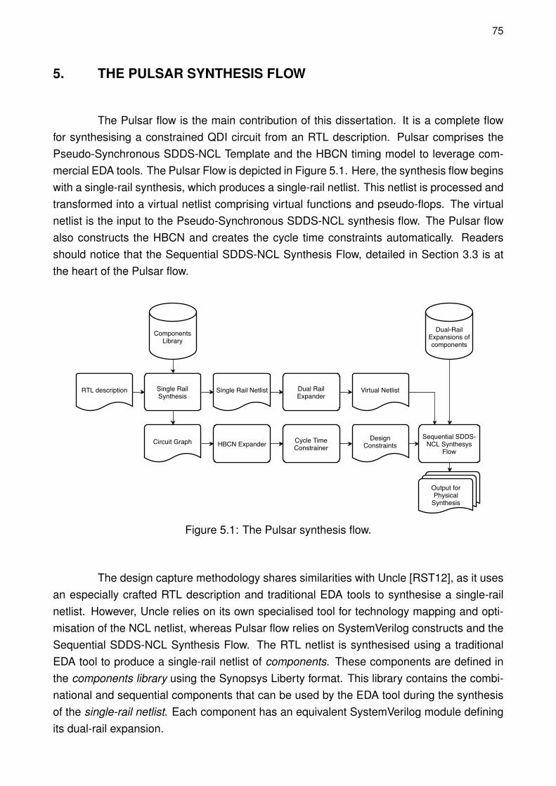
75
5. THE PULSAR SYNTHESIS FLOW
The Pulsar flow is the main contribution of this dissertation. It is a complete flowfor synthesising a constrained QDI circuit from an RTL description. Pulsar comprises thePseudo-Synchronous SDDS-NCL Template and the HBCN timing model to leverage com-mercial EDA tools. The Pulsar Flow is depicted in Figure 5.1. Here, the synthesis flow beginswith a single-rail synthesis, which produces a single-rail netlist. This netlist is processed andtransformed into a virtual netlist comprising virtual functions and pseudo-flops. The virtualnetlist is the input to the Pseudo-Synchronous SDDS-NCL synthesis flow. The Pulsar flowalso constructs the HBCN and creates the cycle time constraints automatically. Readersshould notice that the Sequential SDDS-NCL Synthesis Flow, detailed in Section 3.3 is atthe heart of the Pulsar flow.
RTL description
ComponentsLibrary
Single RailSynthesis
Single Rail Netlist Dual RailExpander
Virtual Netlist
Circuit Graph HBCN Expander Cycle TimeConstrainer
DesignConstraints
Sequential SDDS-NCL Synthesys
Flow
Dual-RailExpansions ofcomponents
Output forPhysical
Synthesis
Figure 5.1: The Pulsar synthesis flow.
The design capture methodology shares similarities with Uncle [RST12], as it usesan especially crafted RTL description and traditional EDA tools to synthesise a single-railnetlist. However, Uncle relies on its own specialised tool for technology mapping and opti-misation of the NCL netlist, whereas Pulsar flow relies on SystemVerilog constructs and theSequential SDDS-NCL Synthesis Flow. The RTL netlist is synthesised using a traditionalEDA tool to produce a single-rail netlist of components. These components are defined inthe components library using the Synopsys Liberty format. This library contains the combi-national and sequential components that can be used by the EDA tool during the synthesisof the single-rail netlist. Each component has an equivalent SystemVerilog module definingits dual-rail expansion.

76
The dual-rail expansion takes advantage of SystemVerilog interfaces [SDF06] torepresent dual-rail four-phase RTZ channels. These channels interconnect modules imple-menting the dual-rail expansion of components. The SystemVerilog interface is also usedfor constructing the acknowledgement network for channels. A simple tool replaces everywire in the single-rail netlist with a channel to create the virtual netlist. The virtual netlist andthe modules implementing the dual-rail expansion of components are input to the synthesisflow described in Section 3.3.
Concurrent to the creation of the virtual netlist, cycle time constraints are com-puted. The scripts used for the single-rail synthesis produce a structural graph describingthe pipeline topology. This circuit graph is used to model the HBCN of the expanded circuit.The same tool that constructs the HBCN also computes the cycle-time constraint using thelinear programming technique discussed in 4.5.
Each topic taking part on this flow is explored in specific Sections herein. Sec-tion 5.2 covers details on the channel expansion process. The component library and itscomponents are explored in Section 5.3. The Pulsar flow is depicted using a simple example,in Sections 5.4 and 5.6. The automatic construction of the HBCN and the implementation ofthe cycle time constrainer are the subject of Section 5.5
5.1 QDI Synthesis Systems (Related Work)
Balsa [EB02] is a CSP-derived [Hoa78, Hoa85] language and framework for imple-menting asynchronous circuits. The Balsa language comprises primitives for explicit paral-lelism of sequential statements and communication channels. Balsa produces handshakecircuits using a process called syntax-directed translation. Handshake circuits [Ber93] imple-ment control-driven asynchronous circuits. They are composed of handshake componentsconnected by channels. Each handshake component is designed to handshake with theirneighbours sequentially, conditionally or in parallel. The behaviour of handshake compo-nents are directly related to the behaviour of CSP constructs. A handshake circuit can beseen as direct hardware equivalent of a CSP program, controlling the data flow in a datapath.In syntax-directed translation handshake components are selected from a small predefinedset that maps directly onto Balsa language constructs. Each handshake component hasa parameterisable gate-level implementation. The circuit gate-level netlist is generated byapplying the parameters to each component instance and composing the resulting compo-nent gate-level netlists. This approach gives control to the designer, providing one-to-onerelation between language constructs and handshake components. However, the controldriven nature of handshake circuits imposes overheads that hurt performance sensitive ap-plications [PTE05, BTE09]. Data-driven asynchronous circuits provide an interesting lower-overhead alternative to control-driven circuits.

77
Uncle [RST12] is a design flow for producing NCL circuits from RTL descriptions.The first step in the Uncle data-driven design flow is to use a commercial synthesis tool toproduce a single-rail synchronous netlist from the RTL description, using a simple library ofgates composed of 2-input AND/OR/XOR gates, NOT gates, edge sensitive flip-flops andlevel sensitive latches. The single-rail netlist is next expanded to a dual-rail netlist in thefollowing four steps: (i) the clock network is removed; (ii) every net (except the global re-set) is replaced by two nets (for dual-rail encoding) and logic gates are replaced by dual-railNCL equivalents using predefined templates of NCL gates; (iii) single-rail latches are re-placed by a single dual-rail latch and flip-flops are substituted by a sequence of two dual-raillatches; Uncle dual-rail latches are implemented using a resetable NCL2W11OF2 gate (aresetable C-Element) and an NOR, 1-of-2 completion detection gate; (iv) the acknowledgenetwork (backward propagation path) is generated between latches. The generated dual-railnetlist passes through optional optimisation steps that improve performance: (i) cell merg-ing, where a subset of simple connected NCL gates is replaced by a more complex NCLgate; (ii) retiming, a process that attempts to balance the propagation delay of the forwardand backward path by moving logic across latches; and (iii) relaxation, a process in whichNCL gates are replaced by simple combinational gates without compromising the indicationprinciple.
5.2 Dual-rail Channels
As discussed in Section 2.2, handshake channels allow the communication of to-kens between entities in an asynchronous circuit. A producer sends tokens through thechannel and consumers receive it. Once a consumer receives the token, it acknowledgesthe reception. A producer must wait until all consumers connected to it acknowledge thereception of token prior to starting a new transmission.
Each channel is a interconnection between components in an asynchronous circuit.They are analogous to wires in a single-rail netlist, i.e. a single element sends tokens tomultiple elements. But in contrast to a wire, a channel provides synchronisation betweenthese elements. Pulsar dual-rail expansion replaces all wires from the single-rail netlist withchannels. However, a channel is not a simple wire. A channel implementation may requiremultiple wires and some logic.
To this end, this works takes advantage of SystemVerilog interfaces [SDF06]. Aninterface is a SystemVerilog construct that allows abstracting interconnections on a system-level description. They are instantiated and bound to module instances much like wires.However, each interface bundles multiple wires that are part of the same interconnect, e.g.bundling the tokens, address and control lines of a processor bus. Besides wires, interfacesinclude modports, that allow defining how modules connect the interface, e.g. bus master or
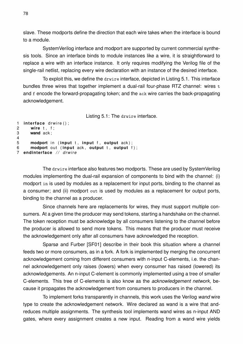
78
slave. These modports define the direction that each wire takes when the interface is boundto a module.
SystemVerilog interface and modport are supported by current commercial synthe-sis tools. Since an interface binds to module instances like a wire, it is straightforward toreplace a wire with an interface instance. It only requires modifying the Verilog file of thesingle-rail netlist, replacing every wire declaration with an instance of the desired interface.
To exploit this, we define the drwire interface, depicted in Listing 5.1. This interfacebundles three wires that together implement a dual-rail four-phase RTZ channel: wires t
and f encode the forward-propagating token; and the ack wire carries the back-propagatingacknowledgement.
Listing 5.1: The drwire interface.1 in ter face drw i re ( ) ;2 wire t , f ;3 wand ack ;45 modport i n ( input t , input f , output ack ) ;6 modport out ( input ack , output t , output f ) ;7 endinterface / / d rw i re
The drwire interface also features two modports. These are used by SystemVerilogmodules implementing the dual-rail expansion of components to bind with the channel: (i)modport in is used by modules as a replacement for input ports, binding to the channel asa consumer; and (ii) modport out is used by modules as a replacement for output ports,binding to the channel as a producer.
Since channels here are replacements for wires, they must support multiple con-sumers. At a given time the producer may send tokens, starting a handshake on the channel.The token reception must be acknowledge by all consumers listening to the channel beforethe producer is allowed to send more tokens. This means that the producer must receivethe acknowledgement only after all consumers have acknowledged the reception.
Sparsø and Furber [SF01] describe in their book this situation where a channelfeeds two or more consumers, as in a fork. A fork is implemented by merging the concurrentacknowledgement coming from different consumers with n-input C-elements, i.e. the chan-nel acknowledgement only raises (lowers) when every consumer has raised (lowered) itsacknowledgements. An n-input C-element is commonly implemented using a tree of smallerC-elements. This tree of C-elements is also know as the acknowledgement network, be-cause it propagates the acknowledgement from consumers to producers in the channel.
To implement forks transparently in channels, this work uses the Verilog wand wiretype to create the acknowledgement network. Wire declared as wand is a wire that and-reduces multiple assignments. The synthesis tool implements wand wires as n-input ANDgates, where every assignment creates a new input. Reading from a wand wire yields
79
the output of the associated n-input AND gate. During synthesis, this n-input AND gate isinterpreted as an and-reduction virtual function.
As discussed in Section 3.1, virtual functions are used to select NCL or NCLP gatesduring synthesis according to required protocol. By design, all channels in the virtual netlistimplement the RTZ protocol. Therefore, the virtual functions associated with the channel areinterpreted as virtual functions of NCL gates. C-elements are valid NCL gates and they canbe selected by their v-function during synthesis. The virtual function of NCL gates is equalto their activation function.
The activation function of an n-input C-element is the and-reduction of its input,i.e. its output changes to one when all inputs are one. Therefore, the and-reduction virtualfunction is realised by an n-input C-element on RTZ. This allows creating the acknowledge-ment network for the channel by setting the ack wire type to wand in the drwire interfacedefinition.
The use of drwire allows the construction of fine-grain channel networks, whereeach channel represents a single dual-rail “bit”. Combinational components bind to channelspassively, they manipulate tokens and propagate acknowledgements between their inboundand outbound channels. Conversely, sequential components bind to channels as active pro-ducers and consumers. They consume tokens from their inbound channels and commencehandshaking on their outbound channels.
The construction of this fine-grain channel network allows handshakes to be per-formed only where data dependency exists. Parallel independent channels in a bus cancomplete their handshakes concurrently. This allows for instance that individual bits in anadder complete handshaking as soon as their computation is ready, regardless the compu-tation status of other bits.
5.3 A Library of Components
The synthesis of a sequential SDDS-NCL circuit with the Pulsar flows starts withthe synthesis of a single-rail netlist. This single-rail netlist comprises sequential and com-binational components from the component library. During single-rail synthesis, these com-ponents are presented to the synthesis tool as cell models using a Synopsys Liberty file.However, these bear no physical layout. Instead each component is expanded by a System-Verilog module that binds to channels implemented by the drwire interface.
Combinational components binds passively to their input and output channels. Thismeans that they do not complete handshakes, instead they act as a passive consumers andproducers. Combinational components combine tokens from their input channels on theoutput channel. They also propagate the acknowledgement between their output and input
80
channels. Conversely, sequential components are active handshaking elements that controlthe propagation of tokens in the pipeline. They complete handshakes between their inputand output channels.
These SystemVerilog modules are instantiated by the virtual netlist. The contentof these modules are used during the synthesis process to implement the circuit usingthe Pseudo-Synchronous SDDS-NCL template. Combinational components are expandedusing virtual functions and sequential components are expanded to pseudo-synchronousWCHB registers. The following Sections cover the expansion of each component type.
5.3.1 Combinational Components
To understand how the expansion of a combinational element is constructed, con-sider the expansion of a nand2 gate. This is a passive element that binds to drwire channels.Since the drwire interface implements dual-rail RTZ encoded channels, a component ex-pansion needs to implement adequate delay insensitive logic to manipulate dual-rail RTZcodewords. The component corresponds to a 2-input NAND gate. The truth table for itssingle-rail equivalent is depicted in Figure 5.2a. It implements the function y = ¬(a∧ b). Theimplementation is not delay insensitive, as it does not differentiate intermediary computa-tions from final computation results.
Remember the discussion about delay insensitive codes in Section 2.3. To make itdelay insensitive, it is necessary to encode the gate input and output with a delay insensitive(DI) code. For this purpose, it is possible to use the 3NCL code presented by Fant in [Fan05].This code introduces a null (N) codeword, alongside the traditional true (T ) and false (F )valid Boolean values. Each codeword encodes a token that propagates in channels.
The 3NCL code table of the gate is depicted in Figure 5.2b. In this expansion, thevalues from the single-rail truth table are mapped to codewords of 3NCL: 1 maps to T and0 maps to F . As a requirement of QDI circuits, logic must be transparent to the channelhandshake. This requirement implies that the state of the output channel of a combinationalelement must indicate the state of its input channels. This is guaranteed by implementinga strong-indicating component, meaning that the component output must only become valid(T or F ) when all inputs are valid and must become null (N) only when all inputs are null. Toimplement a strong-indicating component, it is possible to introduce a hysteresis behaviourto the output. This means that the component output holds its previous value unless all inputare null or all are valid. This guarantees that when a valid (null) output is detected, all inputsare valid (null).
This 3-valued logic is not implementable using CMOS conventional gates. How-ever, it is possible to encode 3NCL codewords using a dual-rail code. Section 2.3 reviewedtwo possible dual-rail codes, each suitable to a matching protocol. The return-to-one (RTO)

81
ay 1 0
b 1 0 10 1 1
(a) Single-rail Boolean truth table.
ay T F N
bT F T -F T T -N - - N
(b) 3NCL code table.
Figure 5.2: Expansion of the nand2 gate from: (a) a single-rail Boolean truth table to (b) a3NCL code table. In the tables, (-) indicates hysteretic behaviour.
dual-rail code is employed when the channel implements the RTO protocol and the return-to-zero (RTZ) protocol is used when the channel implements the RTZ protocol. Figure 5.3depicts the mapping between Boolean, 3NCL and dual-rail RTZ and RTO codes.
Boolean 3NCLDual-Rail
RTZ RTOt f t f
1 T 1 0 0 10 F 0 1 1 0
N 0 0 1 1
Figure 5.3: Map between codes. Only valid codewords are depicted.
A dual-rail code uses two wires to encode tokens. Of course there are 4 possiblecombination of Boolean values that can be encoded with 2 wires. However, DI codes requirethat no codeword is contained in another [Ver88], which limits possible DI codewords to2. Dual-rail RTZ is a bitwise one-hot code (each bit is one-hot coded), where each validcodeword is represented by rising its respective rail and the null codeword is representedby setting both rails low. Rising both rails is considered an invalid codeword, this invalidcodeword can be use during the expansion as a “don’t-care” to minimise logic.
The code table for the dual-rail RTZ encoding of the NAND2 gate is depicted inFigure 5.4. This table establishes how output y behaves as a function of inputs a and b. Onthe left-hand side it depicts 3NCL codewords and on the right-hand side appears their dual-rail RTZ equivalents. Each line establishes possible output values for each input minterm.There are three possibilities contemplated for each output rail: (-) hold the previous value;(1) the output is high; (0) the output is low. Note that it requires 16 minterms to cover the4 input rails, but there are only 9 valid codewords combinations. The missing minterms canbe associated to any value on the output rails. This is not a problem since invalid codewordsare not expected to occur during normal circuit operation and this allows us to simplify thecircuit implementing this code table.
It is interesting to analyse each line type in the code table. The first line capturesthe reset phase of the component, when both inputs are null the output rails are driven low.The next four lines state that if any of the inputs are null the output must hold its previousvalue. In the next four lines all inputs are valid. These lines capture the behaviour of the

82
3NCL Dual-rail RTZa b y a.t a.f b.t b.f y.t y.fN N N 0 0 0 0 0 0N F - 0 0 0 1 - -/0N T - 0 0 1 0 - -F N - 0 1 0 0 - -/0T N - 1 0 0 0 - -F F T 0 1 0 1 1 -/0F T T 0 1 1 0 1 -/0T F T 1 0 0 1 1 -/0T T F 1 0 1 0 -/0 1
Figure 5.4: Dual-rail RTZ code table of the NAND2 gate with equivalent 3NCL codewords.Here, (-) means hold the previous value and (-/0) means that either: hold the previous value,or set it low.
component evaluation phase. When the component is expected to set the output to T itdrives the true rail high and when evaluating to F it drives the false rail high.
Note that some lines indicate that one of the output rails can either hold its previousvalue or go to a certain specific value. This is allowed because the protocol alternatesevaluation and reset phases, thus guaranteeing that under correct operating condition thevalue of some output rails can be assumed. For instance, the reset phase always resetsthe rails to a known null value prior to the evaluation phase. Therefore, driving a single railand holding the state of the other during evaluation is enough to produce a valid dual-railcodeword on the output. A similar situation occurs on the reset phase, when the evaluationis known to not have changed a certain output rail. For instance, in the gate in question, thefalse rail is only risen when both input codewords are T , therefore it must only hold its stateon the reset phase if one of the inputs are T . If one input is F and the other is N, it is safe toassume that the false output rail is 0.
From this code table it is possible to establish two hysteretic functions, each im-plementing the behaviour of an output rail. Remembering from Section 3.1, an hystereticfunction can be described using three minterm sets: (i) the ON-set contain all minterms thatforce the output high (1); (ii) the OFF-set contains all minterms that force the output low (0);and (iii) the HOLD-set contain all minterms that keep the previous value in the output (-).The output rail functions are depicted in Figure 5.5. Each of them captures the behaviourof the output rails in the code table. These functions are minimised, but they still respectthe values on the code table. For instance, the function of the output rail, depicted in Fig-ure 5.5a, depends only on two variables but it satisfies all values associated with the falserail on Figure 5.4.
Functions operating on the channel must by strictly unate. A strictly unate hystereticfunction must change its output in response only to one direction of stimuli on its input.Seeing that during the reset phase the rails of a channel are driven in one direction and
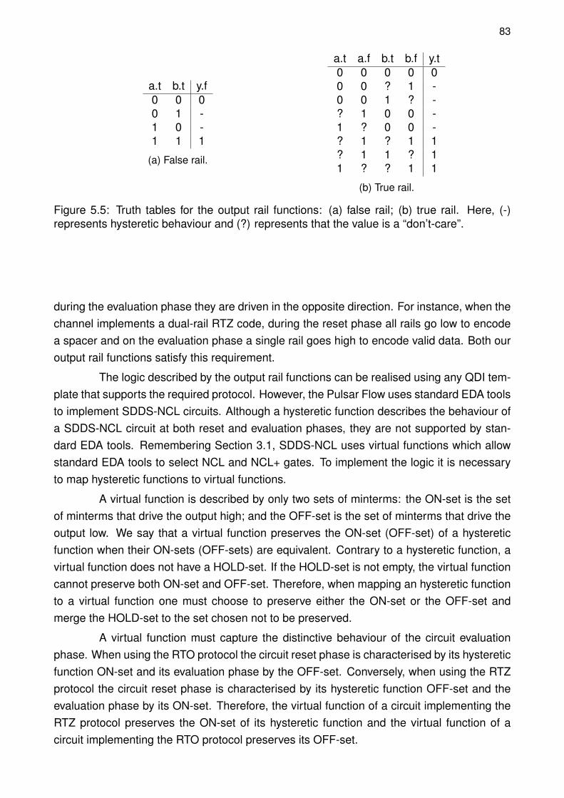
83
a.t b.t y.f0 0 00 1 -1 0 -1 1 1
(a) False rail.
a.t a.f b.t b.f y.t0 0 0 0 00 0 ? 1 -0 0 1 ? -? 1 0 0 -1 ? 0 0 -? 1 ? 1 1? 1 1 ? 11 ? ? 1 1
(b) True rail.
Figure 5.5: Truth tables for the output rail functions: (a) false rail; (b) true rail. Here, (-)represents hysteretic behaviour and (?) represents that the value is a “don’t-care”.
during the evaluation phase they are driven in the opposite direction. For instance, when thechannel implements a dual-rail RTZ code, during the reset phase all rails go low to encodea spacer and on the evaluation phase a single rail goes high to encode valid data. Both ouroutput rail functions satisfy this requirement.
The logic described by the output rail functions can be realised using any QDI tem-plate that supports the required protocol. However, the Pulsar Flow uses standard EDA toolsto implement SDDS-NCL circuits. Although a hysteretic function describes the behaviour ofa SDDS-NCL circuit at both reset and evaluation phases, they are not supported by stan-dard EDA tools. Remembering Section 3.1, SDDS-NCL uses virtual functions which allowstandard EDA tools to select NCL and NCL+ gates. To implement the logic it is necessaryto map hysteretic functions to virtual functions.
A virtual function is described by only two sets of minterms: the ON-set is the setof minterms that drive the output high; and the OFF-set is the set of minterms that drive theoutput low. We say that a virtual function preserves the ON-set (OFF-set) of a hystereticfunction when their ON-sets (OFF-sets) are equivalent. Contrary to a hysteretic function, avirtual function does not have a HOLD-set. If the HOLD-set is not empty, the virtual functioncannot preserve both ON-set and OFF-set. Therefore, when mapping an hysteretic functionto a virtual function one must choose to preserve either the ON-set or the OFF-set andmerge the HOLD-set to the set chosen not to be preserved.
A virtual function must capture the distinctive behaviour of the circuit evaluationphase. When using the RTO protocol the circuit reset phase is characterised by its hystereticfunction ON-set and its evaluation phase by the OFF-set. Conversely, when using the RTZprotocol the circuit reset phase is characterised by its hysteretic function OFF-set and theevaluation phase by its ON-set. Therefore, the virtual function of a circuit implementing theRTZ protocol preserves the ON-set of its hysteretic function and the virtual function of acircuit implementing the RTO protocol preserves its OFF-set.

84
The example output rail functions are hysteretic functions that describe a circuitimplementing the RTZ protocol. Therefore, the virtual functions for its output rails must pre-serve the ON-set of the hysteretic function and merge the HOLD-set with the OFF-set. Thevirtual functions for these output rails are depicted in Figure 5.6. Here, each function risesits output under the same input as the hysteresis functions. However, under the conditionsthat the hysteresis function holds its output, the virtual function drives its output low. Thisis not an issue, since the fix X-Netlist algorithm guarantees that the reset phase is correctlyimplemented.
a.t b.t y.f0 ? 0? 0 01 1 1
(a) False rail.
a.t a.f b.t b.f y.t? 0 ? 0 00 0 ? 1 0? 1 0 0 0? 1 ? 1 1? 1 1 ? 11 ? ? 1 1
(b) True rail.
Figure 5.6: Truth tables for the output rail virtual functions: (a) false rail; (b) true rail. Here,(?) represents that the input value is a “don’t-care”.
To map virtual functions during synthesis, these are represented as Boolean ex-pressions. Each of these expressions are assigned to an output rail in the expansion mod-ule. This module, depicted in Listing 5.2, is implemented using SystemVerilog. The portsfor the module are channels implemented using drwire interfaces. Input ports are declaredusing the drwire.in modport and outputs are declared using drwire.out modport. The ac-knowledgement of the output channel is connected directly to the acknowledgement of inputchannels. This module is instantiated by the virtual netlist during the sequential SDDS-NCLsynthesis.
Listing 5.2: The nand2 expanded module.1 module nand22 ( d rw i re . i n a ,3 drw i re . i n b ,4 drw i re . out y ) ;56 assign y . t = a . f & b . f |7 a . f & b . t |8 a . t & b . f ;9
10 assign y . f = a . t & b . t ;1112 assign a . ack = y . ack ;13 assign b . ack = y . ack ;14 endmodule / / nand2
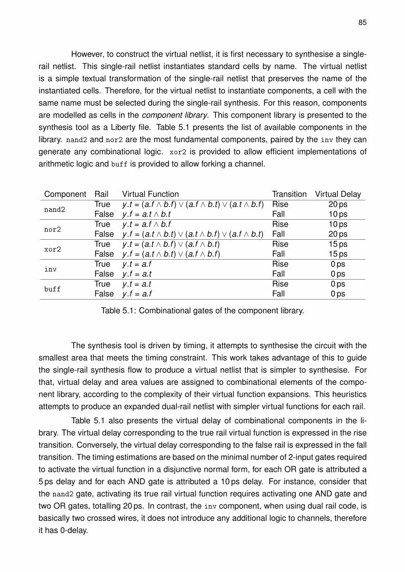
85
However, to construct the virtual netlist, it is first necessary to synthesise a single-rail netlist. This single-rail netlist instantiates standard cells by name. The virtual netlistis a simple textual transformation of the single-rail netlist that preserves the name of theinstantiated cells. Therefore, for the virtual netlist to instantiate components, a cell with thesame name must be selected during the single-rail synthesis. For this reason, componentsare modelled as cells in the component library. This component library is presented to thesynthesis tool as a Liberty file. Table 5.1 presents the list of available components in thelibrary. nand2 and nor2 are the most fundamental components, paired by the inv they cangenerate any combinational logic. xor2 is provided to allow efficient implementations ofarithmetic logic and buff is provided to allow forking a channel.
Component Rail Virtual Function Transition Virtual Delay
nand2True y .t = (a.f ∧ b.f ) ∨ (a.f ∧ b.t) ∨ (a.t ∧ b.f ) Rise 20 psFalse y .f = a.t ∧ b.t Fall 10 ps
nor2True y .t = a.f ∧ b.f Rise 10 psFalse y .f = (a.t ∧ b.t) ∨ (a.t ∧ b.f ) ∨ (a.f ∧ b.t) Fall 20 ps
xor2True y .t = (a.t ∧ b.f ) ∨ (a.f ∧ b.t) Rise 15 psFalse y .f = (a.t ∧ b.t) ∨ (a.f ∧ b.f ) Fall 15 ps
invTrue y .t = a.f Rise 0 psFalse y .f = a.t Fall 0 ps
buffTrue y .t = a.t Rise 0 psFalse y .f = a.f Fall 0 ps
Table 5.1: Combinational gates of the component library.
The synthesis tool is driven by timing, it attempts to synthesise the circuit with thesmallest area that meets the timing constraint. This work takes advantage of this to guidethe single-rail synthesis flow to produce a virtual netlist that is simpler to synthesise. Forthat, virtual delay and area values are assigned to combinational elements of the compo-nent library, according to the complexity of their virtual function expansions. This heuristicsattempts to produce an expanded dual-rail netlist with simpler virtual functions for each rail.
Table 5.1 also presents the virtual delay of combinational components in the li-brary. The virtual delay corresponding to the true rail virtual function is expressed in the risetransition. Conversely, the virtual delay corresponding to the false rail is expressed in the falltransition. The timing estimations are based on the minimal number of 2-input gates requiredto activate the virtual function in a disjunctive normal form, for each OR gate is attributed a5 ps delay and for each AND gate is attributed a 10 ps delay. For instance, consider thatthe nand2 gate, activating its true rail virtual function requires activating one AND gate andtwo OR gates, totalling 20 ps. In contrast, the inv component, when using dual rail code, isbasically two crossed wires, it does not introduce any additional logic to channels, thereforeit has 0-delay.
86
5.3.2 Sequential Components
Another class of components used during the dual-rail expansion are sequentialcomponents. These implement registers in asynchronous pipelines. They are modelled asflip-flops on the single-rail synthesis, allowing standard synthesis tools to instantiate themfrom canonical RTL constructions. The sequential components expand to dual-rail pseudo-synchronous WCHB registers, providing endpoints to be used during the sequential SDDS-NCL synthesis. Sequential elements bind to drwire channels actively, performing hand-shake on their input and output channels. There are three sequential components in theLibrary: (i) the dff half-buffer dual-rail RTZ register; (ii) the dffr resetable full-buffer com-ponent; and (iii) the dffs settable full-buffer component. These components are explored inthe next paragraphs.
From a high-level perspective, registers allow sequential parallelism. They controlthe propagation of tokens in the pipeline, allowing subsequent stages to perform handshakeconcurrently. A half-buffer register achieves this by allowing its input and output channelsto be in opposite handshake phases. The half-buffer register latches tokens, either valid ornull, until both channels finish their handshake phase. This is controlled by incoming outputacknowledgement and data availability in the inputs. When the register latches a new tokenon its output channel, it acknowledges the reception to the channel, thus allowing a newhandshake phase to occur.
The implementation of a half-buffer dual-rail RTZ register is depicted in Figure 5.7a.The half-buffer register is the simplest sequential component and is the base for constructingpipelines. It connects to two channels, an input channel (d) and an output channel (q). Thehalf-buffer consists of: two resetable C-Elements, here named using the NCL-style thresholdgate denomination RNCL2OF2; one OR gate (NCL1OF2); and an inverter. When the outputchannel acknowledges the reception of a null (valid) token, the resetable C-Elements canlatch an incoming valid (null) token. This register operates on RTZ channels, valid tokencodewords are one-hot and null token codewords are presented by all bits in 0. Therefore,an OR gate acknowledges when either a valid or null token has been latched in the inputchannel. A null token is acknowledged by lowering the ack wire of the input channel and avalid token is acknowledged by rising the same signal. The inverter on the output ack wireenables the alternation between reset and evaluation phases.
During initialisation it is important to place the circuit in a known state. This is duethe fact that all components in the circuit consist of gates with hysteresis, which start atunknown initial states. A QDI circuit with an unknown state may not operate properly, asit may contain invalid codewords and possibly inconsistent handshake signal values on itschannels. Both RTZ and RTO protocols require that combinational components outputs are

87
null prior to entering the evaluation phase. Thus, it is important to initialise all combinationalcomponents in the circuit by propagating the null codeword.
For the reason stated above, half-buffer registers employ resetable C-Elementsthat initialise their output channels to null codewords. Null codewords propagate throughcombinational components in cascade, placing the forward propagation logic in a well-knownstate. Similarly, the backward propagation logic on the input channel must also be initialised.When the register initiates the output rails low, the OR gate sets the acknowledgement signalof the input channel low. This signals that the channel is ready to receive new data, aninformation which cascades in the backward propagation of the inbound channel, initialisingit. This is evident when the HBCN model depicted in Figure 5.7b is analysed. Here, theinbound channel is represented by four places preceding the register and the outbound byfour places succeeding the register. The initial marking represents the initial state of thechannel, it marks that both channels are ready to accept new data tokens.
RNCL2OF2
NCL1OF2
q.f
q.t
q.ack
reset
d.ack
d.f
d.t RNCL2OF2
(a) Implementation schematic.
reg
reg'
in
in'
out
out'(b) The half-buffer HBCN model.
Figure 5.7: The dff half-buffer dual-rail register: (a) schematic; (b) HBCn model.
Sometimes it is necessary to initialise a circuit with data. For example, a countermust initialise to a known data value. This implies initialising some channels with validtokens. This can be achieved using the full-buffer components depicted in Figure 5.8. Thesettable full-buffer component, depicted in Figure 5.8a, places a valid true data token in thecircuit. The resetable full-buffer component, depicted in Figure 5.8b, places a valid false datatoken in the circuit. A full-buffer component can simultaneously hold a valid and a null token.This separates their inbound and outbound channels by a full handshake cycle.
The full-buffer component comprises three half-buffer registers in sequence. Theseare required to place valid and a null token in the pipeline while correctly initialising the in-bound and outbound channels. Propagating valid tokens in a circuit at an unknown statewould yield invalid results. Therefore, the first and the last are regular half-buffer registersthat reset to null. These two registers are responsible for initialising the inbound and out-

88
RNCL2OF2
NCL1OF2
NCL1OF2
set
d.ack
d.f
d.t
NCL1OF2
q.f
q.t
q.ack
RNCL2OF2
RNCL2OF2
SNCL2OF2
RNCL2OF2
RNCL2OF2
(a) The dffs settable component.
RNCL2OF2
NCL1OF2
NCL1OF2
reset
d.ack
d.f
d.t
NCL1OF2
q.f
q.t
q.ack
RNCL2OF2
SNCL2OF2
RNCL2OF2
RNCL2OF2
RNCL2OF2
(b) The dffr resettable component.
r2
r2'
r1
r1'
r0
r0'
out
out'
in
in'(c) The full-buffer HBCN model.
Figure 5.8: The two full-buffer components: (a) DFF with set ; (b) DFF with reset ; (c) theHBCN model.

89
bound channels. Due to the provided isolation, the middle register can safely reset to avalid token without compromising circuit initialisation. This is implemented by instantiating asettable C-Element (SNCL2OF2) for either the true or the false rail depending on the com-ponent.
The behaviour of full-buffer components is further evidenced by an analysis of itsHBCN model, depicted in Figure 5.8c. Here, the inbound and outbound channels are ini-tialised to a state where both are ready to accept new tokens, similar to the initial state ofthe half-buffer register. However, two channels internal to the component are initialised to avalid and a null tokens. These internal channels contain no logic, thus they do not need tobe initiated by a null token.
The settable and resettable C-elements employed in full-buffer components arepseudo-flop instances. Remembering Section 3.2, a pseudo-flop allows breaking the cyclesof WCHB pipelines and using STA to analyse the forward and backward propagation paths.This is important during the sequential SDDS-NCL synthesis. However, a commercial EDAtool cannot infer these gates from virtual functions, as it does with NCL and NCLP gatesemployed in combinational component expansions. Therefore, these pseudo-flops are man-ually instantiated in the SystemVerilog module implementing the component expansion. Thismakes the implementation of sequential component expansions technology dependent.
Just as in the case of combinational components, the sequential components arealso instantiated by name during the single-rail synthesis. They are modelled as D-typeflip-flops in the component library Liberty file. The settable and resettable full-buffer compo-nents are modelled as flops with preset and reset, respectively. The half-buffer register ismodelled as a D-type flip-flop with neither reset nor preset control signals. This approachcontrasts with Uncle [RST12], where half-buffer registers are modelled as latches. Note thataccording to the author’s experience, standard EDA tools do not support retiming latch cir-cuits. Therefore, modelling sequential components as flops additionally enables performingretiming during single-rail synthesis. This balances the amount of components employed ineach pipeline stage and opens new opportunities for optimisation in early synthesis steps.
5.4 A Case Study: Applying the Dual Rail Expansion Flow
After presenting the building blocks of the design capture and dual-rail expansionprocesses, it is now possible demonstrating the dual rail expansion flow with a simple ex-ample. This example assumes the synthesis of a 2-bit 2-stage adder, an example simpleenough for the reader to follow through all steps of the expansion.
The starting point for synthesis is the Verilog RTL description. Listing 5.3 depictsthe example RTL. The description must contain a clock port named clk. This clock is used
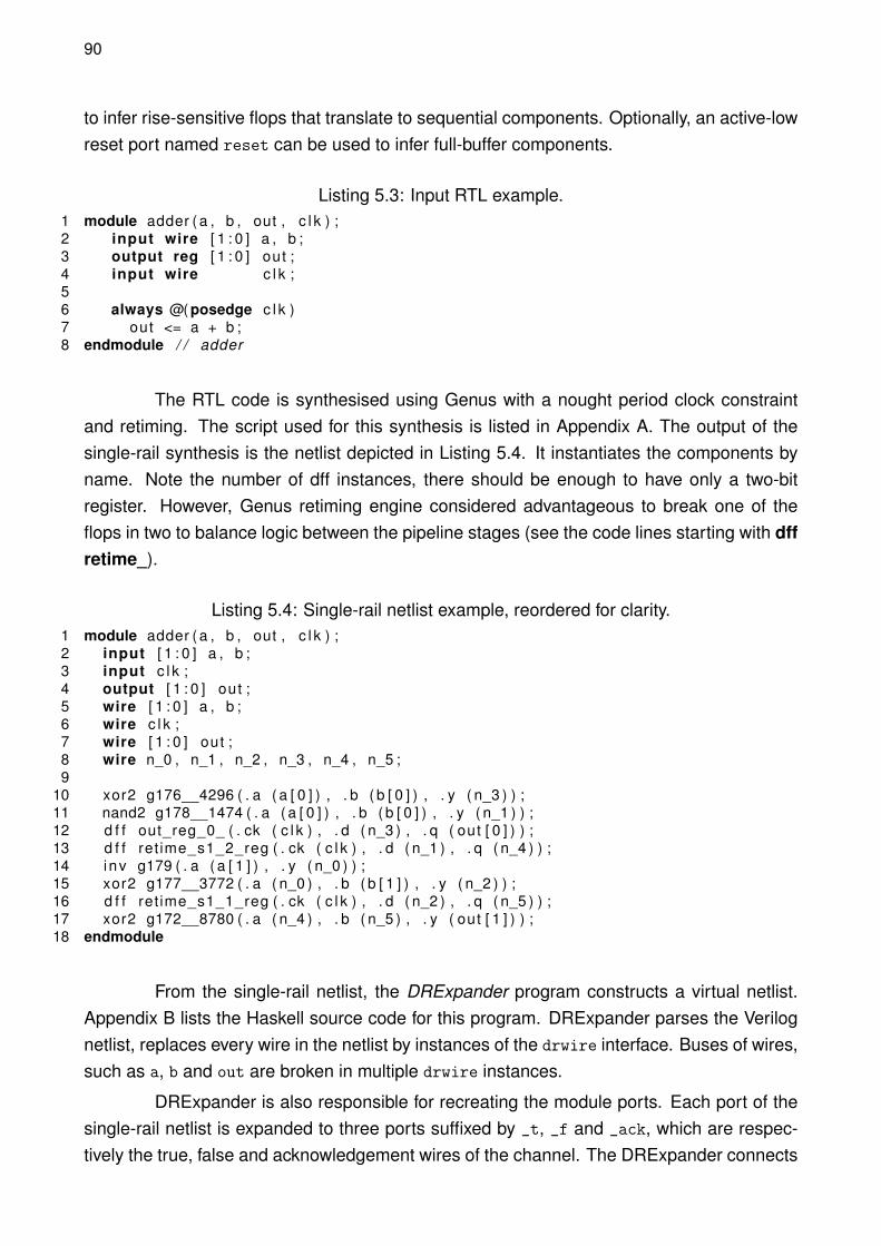
90
to infer rise-sensitive flops that translate to sequential components. Optionally, an active-lowreset port named reset can be used to infer full-buffer components.
Listing 5.3: Input RTL example.1 module adder ( a , b , out , c l k ) ;2 input wire [ 1 : 0 ] a , b ;3 output reg [ 1 : 0 ] out ;4 input wire c l k ;56 always @( posedge c l k )7 out <= a + b ;8 endmodule / / adder
The RTL code is synthesised using Genus with a nought period clock constraintand retiming. The script used for this synthesis is listed in Appendix A. The output of thesingle-rail synthesis is the netlist depicted in Listing 5.4. It instantiates the components byname. Note the number of dff instances, there should be enough to have only a two-bitregister. However, Genus retiming engine considered advantageous to break one of theflops in two to balance logic between the pipeline stages (see the code lines starting with dffretime_).
Listing 5.4: Single-rail netlist example, reordered for clarity.1 module adder ( a , b , out , c l k ) ;2 input [ 1 : 0 ] a , b ;3 input c l k ;4 output [ 1 : 0 ] out ;5 wire [ 1 : 0 ] a , b ;6 wire c l k ;7 wire [ 1 : 0 ] out ;8 wire n_0 , n_1 , n_2 , n_3 , n_4 , n_5 ;9
10 xor2 g176__4296 ( . a ( a [ 0 ] ) , . b ( b [ 0 ] ) , . y ( n_3 ) ) ;11 nand2 g178__1474 ( . a ( a [ 0 ] ) , . b ( b [ 0 ] ) , . y ( n_1 ) ) ;12 d f f out_reg_0_ ( . ck ( c l k ) , . d ( n_3 ) , . q ( out [ 0 ] ) ) ;13 d f f ret ime_s1_2_reg ( . ck ( c l k ) , . d ( n_1 ) , . q ( n_4 ) ) ;14 inv g179 ( . a ( a [ 1 ] ) , . y ( n_0 ) ) ;15 xor2 g177__3772 ( . a ( n_0 ) , . b ( b [ 1 ] ) , . y ( n_2 ) ) ;16 d f f ret ime_s1_1_reg ( . ck ( c l k ) , . d ( n_2 ) , . q ( n_5 ) ) ;17 xor2 g172__8780 ( . a ( n_4 ) , . b ( n_5 ) , . y ( out [ 1 ] ) ) ;18 endmodule
From the single-rail netlist, the DRExpander program constructs a virtual netlist.Appendix B lists the Haskell source code for this program. DRExpander parses the Verilognetlist, replaces every wire in the netlist by instances of the drwire interface. Buses of wires,such as a, b and out are broken in multiple drwire instances.
DRExpander is also responsible for recreating the module ports. Each port of thesingle-rail netlist is expanded to three ports suffixed by _t, _f and _ack, which are respec-tively the true, false and acknowledgement wires of the channel. The DRExpander connects

91
these ports to the internal wires of the respective drwire instance. This provides a consistentinterface for the asynchronous module to connect with the external world.
If the single-rail netlist does not include a reset port, the DRExpander creates oneand connects it to all sequential components in the virtual netlist. This is important to resethalf-buffer registers. Remember that half-buffer registers are modelled as D-flip-fops with noreset. On the single-rail netlist, the dff instances do not contain a reset pin. However, theirexpanded module requires a reset to function properly.
Finally, the virtual netlist contains a clock port clk that connects to all its sequentialcomponents. This is the pseudo-clock signal, used to guide the synthesis during the se-quential pseudo-synchronous SDDS-NCL flow. This signal is not implemented in the finalcircuit, it is only present to guide EDA tools to perform the QDI synthesis correctly.
Listing 5.5: Virtual netlist example, edited for clarity.
1 module adder2 ( a_t , a_f , a_ack ,3 b_t , b_f , b_ack ,4 out_t , out_f , out_ack ,5 c lk , rese t ) ;6 input [ 1 : 0 ] a_t , a_f ;7 output [ 1 : 0 ] a_ack ;8 input [ 1 : 0 ] b_t , b_f ;9 output [ 1 : 0 ] b_ack ;
10 output [ 1 : 0 ] out_t , ou t_ f ;11 input [ 1 : 0 ] out_ack ;12 input c lk , rese t ;1314 / / Ins tances of d rw i re f o r i n t e r n a l channels15 drw i re n_0 ( ) ;16 drw i re n_1 ( ) ;17 drw i re n_2 ( ) ;18 drw i re n_3 ( ) ;19 drw i re n_4 ( ) ;20 drw i re n_5 ( ) ;21 drw i re a_0 ( ) ;22 drw i re a_1 ( ) ;23 drw i re b_0 ( ) ;24 drw i re b_1 ( ) ;25 drw i re out_0 ( ) ;26 drw i re out_1 ( ) ;2728 / / Connections between ex te rna l po r t s and drw i re channels29 assign a_0 . t = a_t [ 0 ] ;30 assign a_0 . f = a_f [ 0 ] ;31 assign a_ack [ 0 ] = a_0 . ack ;32 assign a_1 . t = a_t [ 1 ] ;
92
33 assign a_1 . f = a_f [ 1 ] ;34 assign a_ack [ 1 ] = a_1 . ack ;35 assign b_0 . t = b_t [ 0 ] ;36 assign b_0 . f = b_f [ 0 ] ;37 assign b_ack [ 0 ] = b_0 . ack ;38 assign b_1 . t = b_t [ 1 ] ;39 assign b_1 . f = b_f [ 1 ] ;40 assign b_ack [ 1 ] = b_1 . ack ;41 assign ou t_ t [ 0 ] = out_0 . t ;42 assign ou t_ f [ 0 ] = out_0 . f ;43 assign out_0 . ack = out_ack [ 0 ] ;44 assign ou t_ t [ 1 ] = out_1 . t ;45 assign ou t_ f [ 1 ] = out_1 . f ;46 assign out_1 . ack = out_ack [ 1 ] ;4748 / / Component Instances49 xor2 g176__4296 ( . a ( a_0 ) , . b ( b_0 ) , . y ( n_3 ) ) ;50 nand2 g178__1474 ( . a ( a_0 ) , . b ( b_0 ) , . y ( n_1 ) ) ;51 d f f out_reg_0_ ( . rese t ( rese t ) , . ck ( c l k ) , . d ( n_3 ) , . q ( out_0 ) ) ;52 d f f ret ime_s1_2_reg ( . rese t ( rese t ) , . ck ( c l k ) , . d ( n_1 ) , . q ( n_4 ) ) ;53 inv g179 ( . a ( a_1 ) , . y ( n_0 ) ) ;54 xor2 g177__3772 ( . a ( n_0 ) , . b ( b_1 ) , . y ( n_2 ) ) ;55 d f f ret ime_s1_1_reg ( . rese t ( rese t ) , . ck ( c l k ) , . d ( n_2 ) , . q ( n_5 ) ) ;56 xor2 g172__8780 ( . a ( n_4 ) , . b ( n_5 ) , . y ( out_1 ) ) ;57 endmodule / / adder
5.5 The HBCN Construction and the Cycle Time Constraining
The Pulsar flow provides a tool that computes the pseudo-synchronous constraintsused during the sequential pseudo-synchronous synthesis. This tool computes the HBCNmodel that is instrumental to automatically produce the constraints to use during the QDIsynthesis flow.
The HBCN model is calculated from a structural graph extracted from the single-railnetlist. The structural graph is a directed graph that describes the single-rail netlist timingpaths. In this graph, vertices represent sequential components or ports, and each edge inthe graph represents a channel connecting two registers. Since combinational componentsare transparent to the handshaking process, they are abstracted in this representation. Eachvertex has a name, identifying the component it represents. There are three types of ver-tices: (i) Port, as the name implies, used to identify ports; (ii) NullReg, used to identifyhalf-buffer components; and (iii) DataReg, used to identify full-buffer components. The struc-tural graph adjacency list is exported to a file during single-rail synthesis. Each line of thisfile represents a vertex containing its type, name and a list of successor vertices names.
93
Recalling Section 4.3, an HBCN has a formal representation and a marked graphrepresentation. Using the HBCN formal representation, each register or port corresponds toa transition pair; each channel is a relation between two transition pairs; and each channelhas a initial state. The rules governing the relationship between the HBCN formal represen-tation and its characteristic marked graph is covered in Definition 4.3.1.
Since the expansion process is well-defined, it is possible to use the structuralgraph to construct the HBCN. To this end, it suffices to traverse the structural graph, con-structing the HBCN based on the expansion of the components represented by the vertices.For each Port vertex a single transition pair is created, which models the (ideal) environ-ment1. Each NullReg vertex represents a half-buffer register, which is modelled by a tran-sition pair. Each DataReg vertex represents a full-buffer component. These comprise threeregisters in sequence. This is modelled with a sequence of three transitions pairs connectedby two channels, one channel initialising to reqnull and the others initialising to reqdata. Foreach edge, a channel is created from the last transition pair corresponding to the sourcevertex to the first transition pair corresponding to the target vertex.
To understand this process, it is possible to rely on a simple example. The RTLfor the example circuit is depicted in Listing 5.6. This is a simple circuit, a 3-stage full-bufferloop, an xor gate and a half-buffer output register. The virtual netlist for this circuit is depictedin Listing 5.7. This was generated using Genus and the DRExpander program, as discussedin the previous Section. The associated structural graph is depicted in Listing 5.8. This wasautomatically generated by a TCL script running within Genus at the end of the single-railsynthesis. The TCL script code is depicted in Appendix A.
Listing 5.6: RTL for the simple loop example circuit.1 module xorexp ( in , out , c lk , rese t ) ;2 input wire i n ;3 output reg out ;4 input wire c lk , rese t ;5 reg r ;67 always @( posedge c l k or negedge rese t )8 i f ( ! rese t )9 r <= 0;
10 else11 r <= i n ^ r ;1213 always @( posedge c l k )14 out <= r ;15 endmodule / / xorexp
Here, it is possible to notice the relationship between a virtual netlist and the as-sociated structural graph. In the virtual netlist, the channel from the in port connects to the
1An ideal environment provides a input token immediately upon request by any circuit input, and immediatelyconsumes every token produced at any circuit output.

94
Listing 5.7: Virtual netlist for the simple loop example circuit.1 module xorexp ( in_ t , i n_ f , in_ack , out_t , out_f , out_ack , c lk , rese t ) ;2 input c lk , rese t ;3 input i n_ t , i n _ f ;4 output in_ack ;5 input out_t , ou t_ f ;6 output out_ack ;7 drw i re i n ( ) ;8 d rw i re n_0 ( ) ;9 d rw i re out ( ) ;
10 drw i re r ( ) ;11 assign i n . t = i n _ t ;12 assign i n . f = i n _ f ;13 assign in_ack = i n . ack ;14 assign out . t = ou t_ t ;15 assign out . f = ou t_ f ;16 assign out_ack = out . ack ;17 d f f r r_reg ( . rb ( rese t ) , . ck ( c l k ) , . d ( n_0 ) , . q ( r ) ) ;18 xor2 g19__8780 ( . a ( r ) , . b ( i n ) , . y ( n_0 ) ) ;19 d f f out_reg ( . rese t ( rese t ) , . ck ( c l k ) , . d ( r ) , . q ( out ) ) ;20 endmodule / / xorexp
xor2 combinational component, the output channel of which connects to the r_reg full-buffersequential component. This path is covered by in first line of the structural graph, where thein port is declared and r_reg is assigned as its successor. r_reg is a full-buffer sequen-tial component. The output channel feeds both the out_reg half-buffer register and the xor2
combinational component. The xor2 component in turn feeds back the r_reg forming a loop.This is expressed in the third line of the structural graph, where out_reg is declared as afull-buffer sequential component and lists out_reg and r_reg itself as its successors. Thefourth line declares out_reg as a half-buffer register and lists the output port out as its solesuccessor. Finally, the last line declares the output port out. Since it is an output port, thisis a leaf node in the graph. Accordingly, its successor list is empty.
Listing 5.8: Structural graph for the simple loop example circuit.1 Port " po r t : xorexp / i n " [ " i n s t : xorexp / r_reg " ]2 DataReg " i n s t : xorexp / r_reg " [ " i n s t : xorexp / out_reg " , " i n s t : xorexp / r_reg " ]3 NullReg " i n s t : xorexp / out_reg " [ " po r t : xorexp / out " ]4 Port " po r t : xorexp / out " [ ]
Figure 5.9 depicts the HBCN constructed from this structural graph. This HBCNexplicitly shows the 3-stage full-buffer component forming a loop, the input and output tran-sition pairs and the half-buffer register transition pair between the loop and the output. Eachchannel is represented by four places and the marking indicates the initial state of the chan-nels. A merge between two channels, such as the one occurring inside the xor2 component,is captured by the arrival of multiple channels to the same transition pair. This occurs e.g.between in, r_reg/sout and r_reg. A fork happens when a channel feeds multiple compo-

95
nents, which is captured in the HBCN as multiple channels leaving a transition pair. This isdepicted between r_reg/sout, out_reg and r_reg.
r_reg
r_reg'
r_reg/sout'
r_reg/sin
r_reg/sout
r_reg/sin'
in
in'
out_reg'
out_reg
out'
out
Figure 5.9: The HBCN extracted from the structural graph depicted in Listing 5.8.
After constructing the HBCN, it is possible to apply the linear programming (LP)technique presented in Section 4.5 to compute the pseudo-clock and timing exceptions. Itis desirable to use the pseudo-clock to constrain the delays of combinational componentsin the circuit. However, the full-buffer component contains two internal channels comprisingno logic. These internal channels can be individually constrained to a minimal delay value.This minimal delay is parameterisable and depends on the target technology, but it must beenough to cover the delay of a C-element and a NOR gate. The constraining of these pathsto a minimal delay affects the computation of the pseudo-clock. As discussed in Section 4.5,if these take part in a critical cycle, they can allow the pseudo-clock constraint to assume amore relaxed value.
The process of computing the timing constraints is handled by the hbcnConstrainerprogram. The Haskell source code for this program is listed in Appendix C. This programcomputes the HBCN from the structural graph. It uses the HBCN to define the system ofarrival equations constraining the cycle time to a specified target cycle time constraint. Theprogram invokes the GLPK [Fre12] LP solver to solve the system of arrival equations. Fromthe solution provided by GLPK, it produces a Synopsys design constraints (SDC) file. ThisSDC file contains the pseudo-clock constraint used during the synthesis of the virtual netlist.
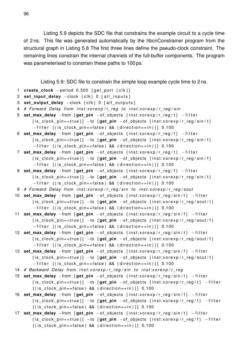
96
Listing 5.9 depicts the SDC file that constrains the example circuit to a cycle timeof 2 ns. This file was generated automatically by the hbcnConstrainer program from thestructural graph in Listing 5.8 The first three lines define the pseudo-clock constraint. Theremaining lines constrain the internal channels of the full-buffer components. The programwas parameterised to constrain these paths to 100 ps.
Listing 5.9: SDC file to constrain the simple loop example cycle time to 2 ns.
1 create_clock −period 0.500 [ ge t_por t { c l k } ]2 set_input_delay −clock { c l k } 0 [ a l l _ i n p u t s ]3 set_output_delay −clock { c l k } 0 [ a l l _ o u t p u t s ]4 # Forward Delay from i n s t : x o r e x p / r_reg to i n s t : x o r e x p / r_reg / s in5 set_max_delay −from [ get_pin −of_objects { i n s t : x o r e x p / r_reg / t } − f i l t e r
{ i s_c lock_p in== t rue } ] −to [ get_pin −of_objects { i n s t : x o r e x p / r_reg / s in / t }− f i l t e r { ( i s_c lock_p in== fa l se ) && ( d i r e c t i o n = = i n ) } ] 0 .100
6 set_max_delay −from [ get_pin −of_objects { i n s t : x o r e x p / r_reg / f } − f i l t e r{ i s_c lock_p in== t rue } ] −to [ get_pin −of_objects { i n s t : x o r e x p / r_reg / s in / f }− f i l t e r { ( i s_c lock_p in== fa l se ) && ( d i r e c t i o n = = i n ) } ] 0 .100
7 set_max_delay −from [ get_pin −of_objects { i n s t : x o r e x p / r_reg / t } − f i l t e r{ i s_c lock_p in== t rue } ] −to [ get_pin −of_objects { i n s t : x o r e x p / r_reg / s in / f }− f i l t e r { ( i s_c lock_p in== fa l se ) && ( d i r e c t i o n = = i n ) } ] 0 .100
8 set_max_delay −from [ get_pin −of_objects { i n s t : x o r e x p / r_reg / f } − f i l t e r{ i s_c lock_p in== t rue } ] −to [ get_pin −of_objects { i n s t : x o r e x p / r_reg / s in / t }− f i l t e r { ( i s_c lock_p in== fa l se ) && ( d i r e c t i o n = = i n ) } ] 0 .100
9 # Forward Delay from i n s t : x o r e x p / r_reg / s in to i n s t : x o r e x p / r_reg / sout10 set_max_delay −from [ get_pin −of_objects { i n s t : x o r e x p / r_reg / s in / t } − f i l t e r
{ i s_c lock_p in== t rue } ] −to [ get_pin −of_objects { i n s t : x o r e x p / r_reg / sout / t }− f i l t e r { ( i s_c lock_p in== fa l se ) && ( d i r e c t i o n = = i n ) } ] 0 .100
11 set_max_delay −from [ get_pin −of_objects { i n s t : x o r e x p / r_reg / s in / f } − f i l t e r{ i s_c lock_p in== t rue } ] −to [ get_pin −of_objects { i n s t : x o r e x p / r_reg / sout / f }− f i l t e r { ( i s_c lock_p in== fa l se ) && ( d i r e c t i o n = = i n ) } ] 0 .100
12 set_max_delay −from [ get_pin −of_objects { i n s t : x o r e x p / r_reg / s in / t } − f i l t e r{ i s_c lock_p in== t rue } ] −to [ get_pin −of_objects { i n s t : x o r e x p / r_reg / sout / f }− f i l t e r { ( i s_c lock_p in== fa l se ) && ( d i r e c t i o n = = i n ) } ] 0 .100
13 set_max_delay −from [ get_pin −of_objects { i n s t : x o r e x p / r_reg / s in / f } − f i l t e r{ i s_c lock_p in== t rue } ] −to [ get_pin −of_objects { i n s t : x o r e x p / r_reg / sout / t }− f i l t e r { ( i s_c lock_p in== fa l se ) && ( d i r e c t i o n = = i n ) } ] 0 .100
14 # Backward Delay from i n s t : x o r e x p / r_reg / s in to i n s t : x o r e x p / r_reg15 set_max_delay −from [ get_pin −of_objects { i n s t : x o r e x p / r_reg / s in / t } − f i l t e r
{ i s_c lock_p in== t rue } ] −to [ get_pin −of_objects { i n s t : x o r e x p / r_reg / t } − f i l t e r{ ( i s_c lock_p in== fa l se ) && ( d i r e c t i o n = = i n ) } ] 0 .100
16 set_max_delay −from [ get_pin −of_objects { i n s t : x o r e x p / r_reg / s in / f } − f i l t e r{ i s_c lock_p in== t rue } ] −to [ get_pin −of_objects { i n s t : x o r e x p / r_reg / f } − f i l t e r{ ( i s_c lock_p in== fa l se ) && ( d i r e c t i o n = = i n ) } ] 0 .100
17 set_max_delay −from [ get_pin −of_objects { i n s t : x o r e x p / r_reg / s in / t } − f i l t e r{ i s_c lock_p in== t rue } ] −to [ get_pin −of_objects { i n s t : x o r e x p / r_reg / f } − f i l t e r{ ( i s_c lock_p in== fa l se ) && ( d i r e c t i o n = = i n ) } ] 0 .100

97
18 set_max_delay −from [ get_pin −of_objects { i n s t : x o r e x p / r_reg / s in / f } − f i l t e r{ i s_c lock_p in== t rue } ] −to [ get_pin −of_objects { i n s t : x o r e x p / r_reg / t } − f i l t e r{ ( i s_c lock_p in== fa l se ) && ( d i r e c t i o n = = i n ) } ] 0 .100
19 # Backward Delay from i n s t : x o r e x p / r_reg / sout to i n s t : x o r e x p / r_reg / s in20 set_max_delay −from [ get_pin −of_objects { i n s t : x o r e x p / r_reg / sout / t } − f i l t e r
{ i s_c lock_p in== t rue } ] −to [ get_pin −of_objects { i n s t : x o r e x p / r_reg / s in / t }− f i l t e r { ( i s_c lock_p in== fa l se ) && ( d i r e c t i o n = = i n ) } ] 0 .100
21 set_max_delay −from [ get_pin −of_objects { i n s t : x o r e x p / r_reg / sout / f } − f i l t e r{ i s_c lock_p in== t rue } ] −to [ get_pin −of_objects { i n s t : x o r e x p / r_reg / s in / f }− f i l t e r { ( i s_c lock_p in== fa l se ) && ( d i r e c t i o n = = i n ) } ] 0 .100
22 set_max_delay −from [ get_pin −of_objects { i n s t : x o r e x p / r_reg / sout / t } − f i l t e r{ i s_c lock_p in== t rue } ] −to [ get_pin −of_objects { i n s t : x o r e x p / r_reg / s in / f }− f i l t e r { ( i s_c lock_p in== fa l se ) && ( d i r e c t i o n = = i n ) } ] 0 .100
23 set_max_delay −from [ get_pin −of_objects { i n s t : x o r e x p / r_reg / sout / f } − f i l t e r{ i s_c lock_p in== t rue } ] −to [ get_pin −of_objects { i n s t : x o r e x p / r_reg / s in / t }− f i l t e r { ( i s_c lock_p in== fa l se ) && ( d i r e c t i o n = = i n ) } ] 0 .100
The hbcnConstrainer program can optionally generate timing exceptions for pathswith free slack, allowing more relaxed timing constraints on paths containing free slack.The previous example was generated with the option to generate these timing exceptionsdisabled. Listing 5.10 depicted the SDC generated by hbcnConstrainer to constraint thesame circuit to the cycle time of 2 ns with the option to relax the paths with free slack enabled.Notice that the pseudo-clock constraint does not change when enabling this option. Here,the maximum delay of each propagation path containing free slack is set by a set_max_delay
timing exception. In this particular case, only the propagation paths internal to the full-buffercomponents have free slack. This is not very useful, but in more complex circuits this freeslack could relax some logic stages.
Listing 5.10: SDC file to constrain the simple loop example cycle time to 2 ns.
1 create_clock −period 0.500 [ ge t_por t { c l k } ]2 set_input_delay −clock { c l k } 0 [ a l l _ i n p u t s ]3 set_output_delay −clock { c l k } 0 [ a l l _ o u t p u t s ]4 # forward delay from i n s t : x o r e x p / r_reg to i n s t : x o r e x p / r_reg / s in5 set_max_delay −from [ get_pin −of_objects { i n s t : x o r e x p / r_reg / t } − f i l t e r
{ i s_c lock_p in== t rue } ] −to [ get_pin −of_objects { i n s t : x o r e x p / r_reg / s in / t }− f i l t e r { ( i s_c lock_p in== fa l se ) && ( d i r e c t i o n = = i n ) } ] 0 .600
6 set_max_delay −from [ get_pin −of_objects { i n s t : x o r e x p / r_reg / f } − f i l t e r{ i s_c lock_p in== t rue } ] −to [ get_pin −of_objects { i n s t : x o r e x p / r_reg / s in / f }− f i l t e r { ( i s_c lock_p in== fa l se ) && ( d i r e c t i o n = = i n ) } ] 0 .600
7 set_max_delay −from [ get_pin −of_objects { i n s t : x o r e x p / r_reg / t } − f i l t e r{ i s_c lock_p in== t rue } ] −to [ get_pin −of_objects { i n s t : x o r e x p / r_reg / s in / f }− f i l t e r { ( i s_c lock_p in== fa l se ) && ( d i r e c t i o n = = i n ) } ] 0 .600
8 set_max_delay −from [ get_pin −of_objects { i n s t : x o r e x p / r_reg / f } − f i l t e r{ i s_c lock_p in== t rue } ] −to [ get_pin −of_objects { i n s t : x o r e x p / r_reg / s in / t }− f i l t e r { ( i s_c lock_p in== fa l se ) && ( d i r e c t i o n = = i n ) } ] 0 .600
9 # forward delay from i n s t : x o r e x p / r_reg / s in to i n s t : x o r e x p / r_reg / sout

98
10 set_max_delay −from [ get_pin −of_objects { i n s t : x o r e x p / r_reg / s in / t } − f i l t e r{ i s_c lock_p in== t rue } ] −to [ get_pin −of_objects { i n s t : x o r e x p / r_reg / sout / t }− f i l t e r { ( i s_c lock_p in== fa l se ) && ( d i r e c t i o n = = i n ) } ] 0 .900
11 set_max_delay −from [ get_pin −of_objects { i n s t : x o r e x p / r_reg / s in / f } − f i l t e r{ i s_c lock_p in== t rue } ] −to [ get_pin −of_objects { i n s t : x o r e x p / r_reg / sout / f }− f i l t e r { ( i s_c lock_p in== fa l se ) && ( d i r e c t i o n = = i n ) } ] 0 .900
12 set_max_delay −from [ get_pin −of_objects { i n s t : x o r e x p / r_reg / s in / t } − f i l t e r{ i s_c lock_p in== t rue } ] −to [ get_pin −of_objects { i n s t : x o r e x p / r_reg / sout / f }− f i l t e r { ( i s_c lock_p in== fa l se ) && ( d i r e c t i o n = = i n ) } ] 0 .900
13 set_max_delay −from [ get_pin −of_objects { i n s t : x o r e x p / r_reg / s in / f } − f i l t e r{ i s_c lock_p in== t rue } ] −to [ get_pin −of_objects { i n s t : x o r e x p / r_reg / sout / t }− f i l t e r { ( i s_c lock_p in== fa l se ) && ( d i r e c t i o n = = i n ) } ] 0 .900
14 # backward delay from i n s t : x o r e x p / r_reg / s in to i n s t : x o r e x p / r_reg15 set_max_delay −from [ get_pin −of_objects { i n s t : x o r e x p / r_reg / s in / t } − f i l t e r
{ i s_c lock_p in== t rue } ] −to [ get_pin −of_objects { i n s t : x o r e x p / r_reg / t } − f i l t e r{ ( i s_c lock_p in== fa l se ) && ( d i r e c t i o n = = i n ) } ] 0 .400
16 set_max_delay −from [ get_pin −of_objects { i n s t : x o r e x p / r_reg / s in / f } − f i l t e r{ i s_c lock_p in== t rue } ] −to [ get_pin −of_objects { i n s t : x o r e x p / r_reg / f } − f i l t e r{ ( i s_c lock_p in== fa l se ) && ( d i r e c t i o n = = i n ) } ] 0 .400
17 set_max_delay −from [ get_pin −of_objects { i n s t : x o r e x p / r_reg / s in / t } − f i l t e r{ i s_c lock_p in== t rue } ] −to [ get_pin −of_objects { i n s t : x o r e x p / r_reg / f } − f i l t e r{ ( i s_c lock_p in== fa l se ) && ( d i r e c t i o n = = i n ) } ] 0 .400
18 set_max_delay −from [ get_pin −of_objects { i n s t : x o r e x p / r_reg / s in / f } − f i l t e r{ i s_c lock_p in== t rue } ] −to [ get_pin −of_objects { i n s t : x o r e x p / r_reg / t } − f i l t e r{ ( i s_c lock_p in== fa l se ) && ( d i r e c t i o n = = i n ) } ] 0 .400
19 # backward delay from i n s t : x o r e x p / r_reg / sout to i n s t : x o r e x p / r_reg / s in20 set_max_delay −from [ get_pin −of_objects { i n s t : x o r e x p / r_reg / sout / t } − f i l t e r
{ i s_c lock_p in== t rue } ] −to [ get_pin −of_objects { i n s t : x o r e x p / r_reg / s in / t }− f i l t e r { ( i s_c lock_p in== fa l se ) && ( d i r e c t i o n = = i n ) } ] 0 .100
21 set_max_delay −from [ get_pin −of_objects { i n s t : x o r e x p / r_reg / sout / f } − f i l t e r{ i s_c lock_p in== t rue } ] −to [ get_pin −of_objects { i n s t : x o r e x p / r_reg / s in / f }− f i l t e r { ( i s_c lock_p in== fa l se ) && ( d i r e c t i o n = = i n ) } ] 0 .100
22 set_max_delay −from [ get_pin −of_objects { i n s t : x o r e x p / r_reg / sout / t } − f i l t e r{ i s_c lock_p in== t rue } ] −to [ get_pin −of_objects { i n s t : x o r e x p / r_reg / s in / f }− f i l t e r { ( i s_c lock_p in== fa l se ) && ( d i r e c t i o n = = i n ) } ] 0 .100
23 set_max_delay −from [ get_pin −of_objects { i n s t : x o r e x p / r_reg / sout / f } − f i l t e r{ i s_c lock_p in== t rue } ] −to [ get_pin −of_objects { i n s t : x o r e x p / r_reg / s in / t }− f i l t e r { ( i s_c lock_p in== fa l se ) && ( d i r e c t i o n = = i n ) } ] 0 .100
5.6 Completing the Case Study Synthesis
After constructing the virtual netlist, it is then possible to synthesise the virtualnetlist using the pseudo-synchronous SDDS-NCL synthesis flow described in Section 3.3.This Section continues the synthesis of the example circuit explored in Section 5.4. For

99
that, the first step is to compute the constraints using the hbcnConstrainer from the previousSection. The structural graph of our example circuit is depicted in Listing 5.11
Listing 5.11: Structural graph of virtual netlist depicted in Listing 5.5.
1 Port " po r t : adder / a [ 1 ] " [ " i n s t : adder / ret ime_s1_1_reg " ]2 Port " po r t : adder / a [ 0 ] " [ " i n s t : adder / out_reg_0_ " , " i n s t : adder / ret ime_s1_2_reg " ]3 Port " po r t : adder / b [ 1 ] " [ " i n s t : adder / ret ime_s1_1_reg " ]4 Port " po r t : adder / b [ 0 ] " [ " i n s t : adder / out_reg_0_ " , " i n s t : adder / ret ime_s1_2_reg " ]5 NullReg " i n s t : adder / ret ime_s1_1_reg " [ " po r t : adder / out [ 1 ] " ]6 NullReg " i n s t : adder / out_reg_0_ " [ " po r t : adder / out [ 0 ] " ]7 NullReg " i n s t : adder / ret ime_s1_2_reg " [ " po r t : adder / out [ 1 ] " ]8 Port " po r t : adder / out [ 0 ] " [ ]9 Port " po r t : adder / out [ 1 ] " [ ]
The hbcnConstrainer program creates an SDC file that constrains this circuit to acycle time of 4 ns. This SDC file is depicted in Listing 5.12. The adder circuit is a very simplelinear pipeline, it contains no free slack when constrained with a pseudo-clock constraint.Enabling the free slack relaxation options does not affect the produced SDC file.
Listing 5.12: SDC file constraining the cycle time of the pipeline adder to 4 ns.
1 create_clock −period 1.000 [ ge t_por t { c l k } ]2 set_input_delay −clock { c l k } 0 [ a l l _ i n p u t s ]3 set_output_delay −clock { c l k } 0 [ a l l _ o u t p u t s ]
The produced SDC, along with the virtual netlist depicted in Listing 5.5 are used asinput to the pseudo-synchronous SDDS-NCL synthesis flow. The virtual netlist is the primarynetlist input to the synthesis flow. Another netlist input is the component expansion library.The SystemVerilog file containing the component expansions and the pseudo-synchronoussynthesis scripts are depicted in Appendix D. The example circuit was synthesised using theASCEND-ST65NCL Library [MOPC11], a library of NCL and NCLP gates targeting STMicro65 nm technology node. The resulting netlist is depicted in Listing 5.13. This netlist wasreordered and commented to highlight its equivalence to the virtual netlist.
Listing 5.13: Sequential SDDS-NCL Netlist, edited for clarity.
1 module adder ( a_t , a_f , a_ack , b_t , b_f , b_ack ,2 out_t , out_f , out_ack , c lk , rese t ) ;3 input wire [ 1 : 0 ] a_t , a_f , b_t , b_f , out_ack ;4 input wire c lk , rese t ;5 output wire [ 1 : 0 ] a_ack , b_ack , out_t , ou t_ f ;6 wire n_1 , n_1_f , n_1_t , n_2_f , n_2_t , n_3 , n_3_f , n_4 ;7 wire n_4_f , n_4_t , n_5 , n_5_f , n_5_t , n_6 , n_7 , n_8 ;8 wire n_9 , n_10 , n_14 ;9
10 / / backward propagat ion l o g i c11 assign b_ack [ 0 ] = a_ack [ 0 ] ;12 assign b_ack [ 1 ] = a_ack [ 1 ] ;
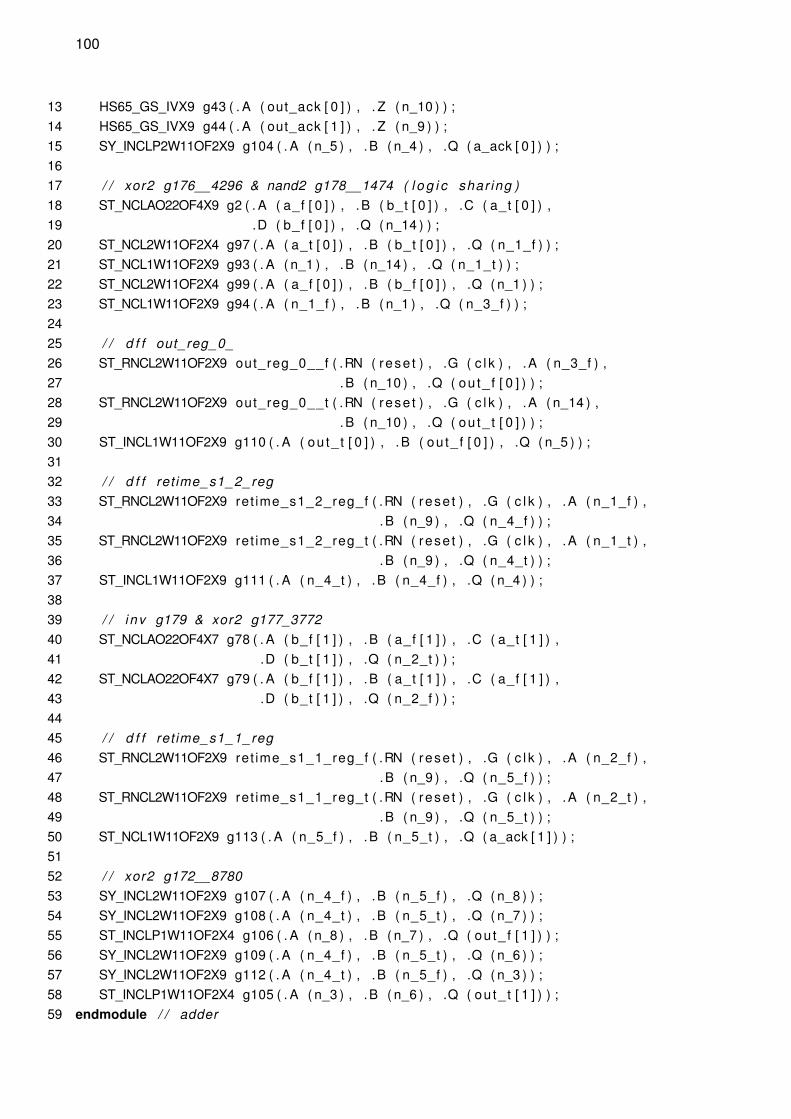
100
13 HS65_GS_IVX9 g43 ( . A ( out_ack [ 0 ] ) , . Z ( n_10 ) ) ;14 HS65_GS_IVX9 g44 ( . A ( out_ack [ 1 ] ) , . Z ( n_9 ) ) ;15 SY_INCLP2W11OF2X9 g104 ( . A ( n_5 ) , .B ( n_4 ) , .Q ( a_ack [ 0 ] ) ) ;1617 / / xor2 g176__4296 & nand2 g178__1474 ( l o g i c shar ing )18 ST_NCLAO22OF4X9 g2 ( . A ( a_f [ 0 ] ) , .B ( b_t [ 0 ] ) , .C ( a_t [ 0 ] ) ,19 .D ( b_f [ 0 ] ) , .Q ( n_14 ) ) ;20 ST_NCL2W11OF2X4 g97 ( . A ( a_t [ 0 ] ) , .B ( b_t [ 0 ] ) , .Q ( n_1_f ) ) ;21 ST_NCL1W11OF2X9 g93 ( . A ( n_1 ) , .B ( n_14 ) , .Q ( n_1_t ) ) ;22 ST_NCL2W11OF2X4 g99 ( . A ( a_f [ 0 ] ) , .B ( b_f [ 0 ] ) , .Q ( n_1 ) ) ;23 ST_NCL1W11OF2X9 g94 ( . A ( n_1_f ) , .B ( n_1 ) , .Q ( n_3_f ) ) ;2425 / / d f f out_reg_0_26 ST_RNCL2W11OF2X9 out_reg_0__f ( .RN ( rese t ) , .G ( c l k ) , .A ( n_3_f ) ,27 .B ( n_10 ) , .Q ( ou t_ f [ 0 ] ) ) ;28 ST_RNCL2W11OF2X9 out_reg_0__t ( .RN ( rese t ) , .G ( c l k ) , .A ( n_14 ) ,29 .B ( n_10 ) , .Q ( ou t_ t [ 0 ] ) ) ;30 ST_INCL1W11OF2X9 g110 ( . A ( ou t_ t [ 0 ] ) , .B ( ou t_ f [ 0 ] ) , .Q ( n_5 ) ) ;3132 / / d f f ret ime_s1_2_reg33 ST_RNCL2W11OF2X9 ret ime_s1_2_reg_f ( .RN ( rese t ) , .G ( c l k ) , .A ( n_1_f ) ,34 .B ( n_9 ) , .Q ( n_4_f ) ) ;35 ST_RNCL2W11OF2X9 ret ime_s1_2_reg_t ( .RN ( rese t ) , .G ( c l k ) , .A ( n_1_t ) ,36 .B ( n_9 ) , .Q ( n_4_t ) ) ;37 ST_INCL1W11OF2X9 g111 ( . A ( n_4_t ) , .B ( n_4_f ) , .Q ( n_4 ) ) ;3839 / / i nv g179 & xor2 g177_377240 ST_NCLAO22OF4X7 g78 ( . A ( b_f [ 1 ] ) , .B ( a_f [ 1 ] ) , .C ( a_t [ 1 ] ) ,41 .D ( b_t [ 1 ] ) , .Q ( n_2_t ) ) ;42 ST_NCLAO22OF4X7 g79 ( . A ( b_f [ 1 ] ) , .B ( a_t [ 1 ] ) , .C ( a_f [ 1 ] ) ,43 .D ( b_t [ 1 ] ) , .Q ( n_2_f ) ) ;4445 / / d f f ret ime_s1_1_reg46 ST_RNCL2W11OF2X9 ret ime_s1_1_reg_f ( .RN ( rese t ) , .G ( c l k ) , .A ( n_2_f ) ,47 .B ( n_9 ) , .Q ( n_5_f ) ) ;48 ST_RNCL2W11OF2X9 ret ime_s1_1_reg_t ( .RN ( rese t ) , .G ( c l k ) , .A ( n_2_t ) ,49 .B ( n_9 ) , .Q ( n_5_t ) ) ;50 ST_NCL1W11OF2X9 g113 ( . A ( n_5_f ) , .B ( n_5_t ) , .Q ( a_ack [ 1 ] ) ) ;5152 / / xor2 g172__878053 SY_INCL2W11OF2X9 g107 ( . A ( n_4_f ) , .B ( n_5_f ) , .Q ( n_8 ) ) ;54 SY_INCL2W11OF2X9 g108 ( . A ( n_4_t ) , .B ( n_5_t ) , .Q ( n_7 ) ) ;55 ST_INCLP1W11OF2X4 g106 ( . A ( n_8 ) , .B ( n_7 ) , .Q ( ou t_ f [ 1 ] ) ) ;56 SY_INCL2W11OF2X9 g109 ( . A ( n_4_f ) , .B ( n_5_t ) , .Q ( n_6 ) ) ;57 SY_INCL2W11OF2X9 g112 ( . A ( n_4_t ) , .B ( n_5_f ) , .Q ( n_3 ) ) ;58 ST_INCLP1W11OF2X4 g105 ( . A ( n_3 ) , .B ( n_6 ) , .Q ( ou t_ t [ 1 ] ) ) ;59 endmodule / / adder

101
6. EXPERIMENTS AND RESULTS
The Pulsar flow was initially validated by synthesising and simulating a set of multi-ply and accumulate (MAC) units under a range of timing constraints. MACs were chosen asexample circuits due to their logic complexity and non-linear pipeline structure. Non-linearpipelines are good case studies for evaluating the HBCN timing constraining capabilities, be-cause they present non-trivial maximum cycle times. The accumulator of a MAC comprisesa circular buffer. This buffer can be implemented with different number of pipeline stages.Four different MAC architectures were thus designed:
• A 3-stage MAC, comprising a 3-stage accumulator.
• A 4-stage MAC, comprising a 4-stage accumulator.
• A 5-stage MAC, comprising a 5-stage accumulator.
• A 6-stage MAC, comprising a 6-stage accumulator.
These MACs present the same interface and behaviour, they multiply two 16-bit numbersfrom the input and add the 32-bit result in an accumulation loop. The new accumulatorvalue is presented to the output after every computation cycle. This allow using the sametestbench for simulating all MACs.
MACs were synthesised using the Pulsar flow from RTL descriptions. The RTLfor the 3-stage MAC is depicted in Listing 6.1. Both inputs and outputs are buffered withhalf-buffer registers. Here, the accumulator loop has the minimal number of stages requiredto correctly operate. Listing 6.2 presents the RTL for the 4-stage MAC. Here, a result
half-buffer register is introduced between the input and output registers. This additionalregister also takes part in the accumulator loop. The RTL for 5-stage and 6-stage MACs arerespectively depicted in Listing 6.3 and in Listing 6.4. Each of these respectively include asecond and a third result registers in the pipeline. Notice that on the RTL description mostpipeline stages are empty. The retiming engine takes care of distributing the logic amongthe empty pipeline stages during single-rail synthesis.
Single-rail synthesis was performed using the Cadence Genus 18.1 tool with retim-ing enabled. The optimisation effort was set to extreme and the circuit was synthesised witha nought clock period constraint. Genus was also configured to optimise the total negativeslack. These settings were used to minimise the logical depth of each pipeline stage. Thesingle-rail synthesis of the RTL descriptions resulted in virtual netlists with the characteris-tics summarised in Table 6.1. Here, the worst virtual delays indicate the complexity of thevirtual function composition for the longest path in the circuit.

102
Listing 6.1: RTL code for the 3-stage MAC.1 module mac #(WIDTH=32)2 ( input logic [ ( WIDTH/ 2 ) −1:0] a , b ,3 input logic c lk , reset ,4 output logic [WIDTH−1:0] out ) ;5 logic [ ( WIDTH/ 2 ) −1:0] reg_a ;6 logic [ ( WIDTH/ 2 ) −1:0] reg_b ;7 logic [WIDTH−1:0] r e s u l t ;8 logic [WIDTH−1:0] acc ;9
10 assign r e s u l t = ( reg_a * reg_b ) + acc ;1112 always @( posedge c l k ) begin13 reg_a <= a ;14 reg_b <= b ;15 out <= r e s u l t ;16 end1718 always @( posedge c l k or negedge rese t )19 i f ( ! rese t )20 acc <= ’ 0 ;21 else22 acc <= r e s u l t ;23 endmodule / / mac
Listing 6.2: RTL code for the 4-stage MAC.1 module mac #(WIDTH=32)2 ( input logic [ ( WIDTH/ 2 ) −1:0] a , b ,3 input logic c lk , reset ,4 output logic [WIDTH−1:0] out ) ;5 logic [ ( WIDTH/ 2 ) −1:0] reg_a ;6 logic [ ( WIDTH/ 2 ) −1:0] reg_b ;7 logic [WIDTH−1:0] r e s u l t ;8 logic [WIDTH−1:0] acc ;9
10 always @( posedge c l k ) begin11 reg_a <= a ;12 reg_b <= b ;13 r e s u l t <= ( reg_a * reg_b ) + acc ;14 out <= r e s u l t ;15 end1617 always @( posedge c l k or negedge rese t )18 i f ( ! rese t )19 acc <= ’ 0 ;20 else21 acc <= r e s u l t ;22 endmodule / / mac
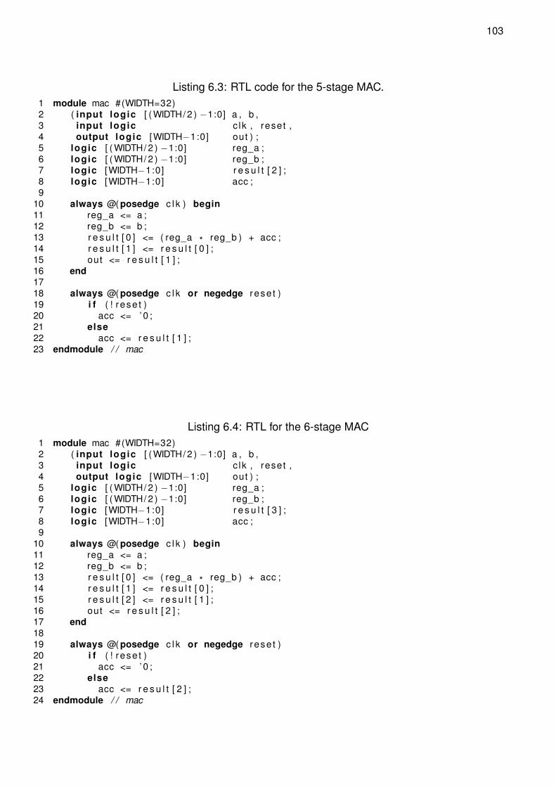
103
Listing 6.3: RTL code for the 5-stage MAC.1 module mac #(WIDTH=32)2 ( input logic [ ( WIDTH/ 2 ) −1:0] a , b ,3 input logic c lk , reset ,4 output logic [WIDTH−1:0] out ) ;5 logic [ ( WIDTH/ 2 ) −1:0] reg_a ;6 logic [ ( WIDTH/ 2 ) −1:0] reg_b ;7 logic [WIDTH−1:0] r e s u l t [ 2 ] ;8 logic [WIDTH−1:0] acc ;9
10 always @( posedge c l k ) begin11 reg_a <= a ;12 reg_b <= b ;13 r e s u l t [ 0 ] <= ( reg_a * reg_b ) + acc ;14 r e s u l t [ 1 ] <= r e s u l t [ 0 ] ;15 out <= r e s u l t [ 1 ] ;16 end1718 always @( posedge c l k or negedge rese t )19 i f ( ! rese t )20 acc <= ’ 0 ;21 else22 acc <= r e s u l t [ 1 ] ;23 endmodule / / mac
Listing 6.4: RTL for the 6-stage MAC1 module mac #(WIDTH=32)2 ( input logic [ ( WIDTH/ 2 ) −1:0] a , b ,3 input logic c lk , reset ,4 output logic [WIDTH−1:0] out ) ;5 logic [ ( WIDTH/ 2 ) −1:0] reg_a ;6 logic [ ( WIDTH/ 2 ) −1:0] reg_b ;7 logic [WIDTH−1:0] r e s u l t [ 3 ] ;8 logic [WIDTH−1:0] acc ;9
10 always @( posedge c l k ) begin11 reg_a <= a ;12 reg_b <= b ;13 r e s u l t [ 0 ] <= ( reg_a * reg_b ) + acc ;14 r e s u l t [ 1 ] <= r e s u l t [ 0 ] ;15 r e s u l t [ 2 ] <= r e s u l t [ 1 ] ;16 out <= r e s u l t [ 2 ] ;17 end1819 always @( posedge c l k or negedge rese t )20 i f ( ! rese t )21 acc <= ’ 0 ;22 else23 acc <= r e s u l t [ 2 ] ;24 endmodule / / mac
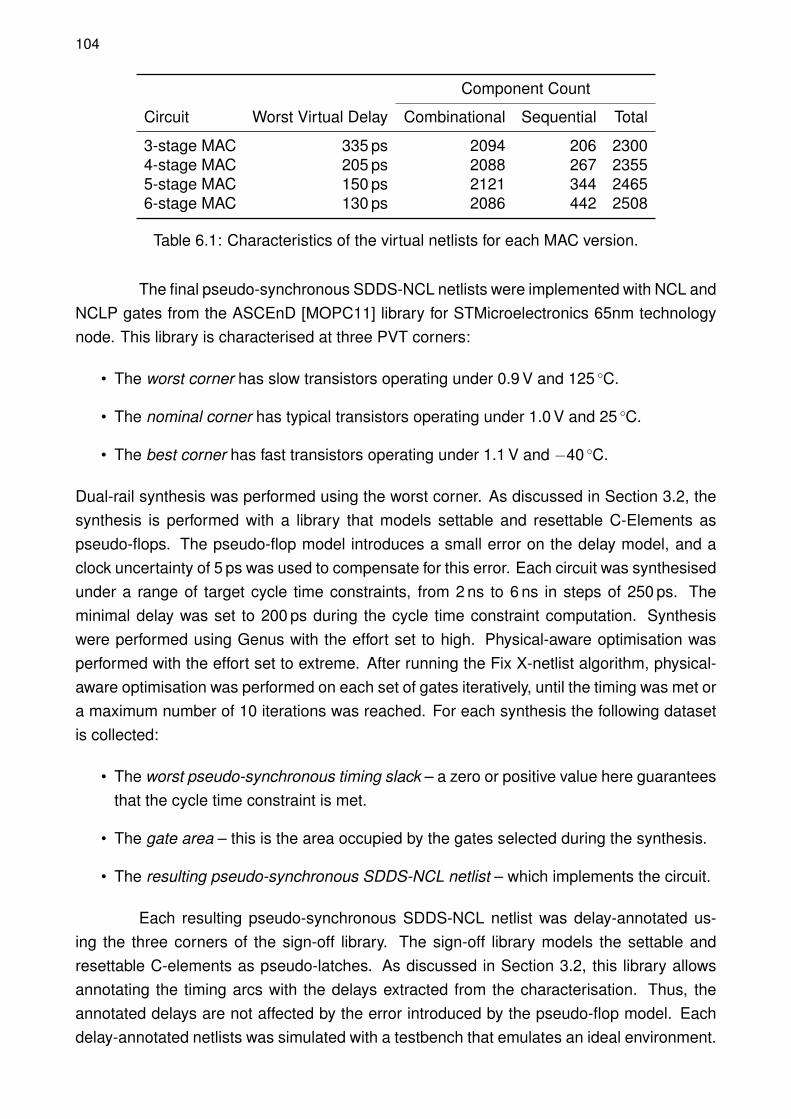
104
Component Count
Circuit Worst Virtual Delay Combinational Sequential Total
3-stage MAC 335 ps 2094 206 23004-stage MAC 205 ps 2088 267 23555-stage MAC 150 ps 2121 344 24656-stage MAC 130 ps 2086 442 2508
Table 6.1: Characteristics of the virtual netlists for each MAC version.
The final pseudo-synchronous SDDS-NCL netlists were implemented with NCL andNCLP gates from the ASCEnD [MOPC11] library for STMicroelectronics 65nm technologynode. This library is characterised at three PVT corners:
• The worst corner has slow transistors operating under 0.9 V and 125 ◦C.
• The nominal corner has typical transistors operating under 1.0 V and 25 ◦C.
• The best corner has fast transistors operating under 1.1 V and −40 ◦C.
Dual-rail synthesis was performed using the worst corner. As discussed in Section 3.2, thesynthesis is performed with a library that models settable and resettable C-Elements aspseudo-flops. The pseudo-flop model introduces a small error on the delay model, and aclock uncertainty of 5 ps was used to compensate for this error. Each circuit was synthesisedunder a range of target cycle time constraints, from 2 ns to 6 ns in steps of 250 ps. Theminimal delay was set to 200 ps during the cycle time constraint computation. Synthesiswere performed using Genus with the effort set to high. Physical-aware optimisation wasperformed with the effort set to extreme. After running the Fix X-netlist algorithm, physical-aware optimisation was performed on each set of gates iteratively, until the timing was met ora maximum number of 10 iterations was reached. For each synthesis the following datasetis collected:
• The worst pseudo-synchronous timing slack – a zero or positive value here guaranteesthat the cycle time constraint is met.
• The gate area – this is the area occupied by the gates selected during the synthesis.
• The resulting pseudo-synchronous SDDS-NCL netlist – which implements the circuit.
Each resulting pseudo-synchronous SDDS-NCL netlist was delay-annotated us-ing the three corners of the sign-off library. The sign-off library models the settable andresettable C-elements as pseudo-latches. As discussed in Section 3.2, this library allowsannotating the timing arcs with the delays extracted from the characterisation. Thus, theannotated delays are not affected by the error introduced by the pseudo-flop model. Eachdelay-annotated netlists was simulated with a testbench that emulates an ideal environment.

105
An ideal environment has no delay of itself, it feeds tokens into the pipeline as soon as anacknowledgement is received and it also acknowledges the reception of tokens instanta-neously, thus isolating the circuit from external delays. Under these conditions, for eachcorner it was possible measuring:
• The output cycle time – this is the time between the reception of two data tokens at thepipeline output.
• The input cycle time – this is the time between the insertion of two successive datatokens in the pipeline input.
• The latency, – this is the time between a the insertion of a data token at the input andthe reception of a corresponding data token with the result at the output.
• The averaged switching activity of the circuit – this is used in conjunction with the circuitnetlist and the sign-off library as input for static power analysis (SPA).
Timing measurements are subject to data-dependent delay variations, as discussed in Sec-tion 4.1. These values are presented here as an average. The standard deviation of themeasured data points is presented as a range around the former average.
Results for the 3-stage MAC are depicted in Figure 6.1. They show the timing ex-tracted through simulation and the data collected from synthesis reports. The worst pseudo-synchronous timing slack for this circuit is depicted in Figure 6.1d. It presents negative slackvalues for cycle time constraints under 5 ns. According to the models, a negative slack valueindicates that it is not possible to guarantee that the cycle time constraint is met. This ismade evident in the results of the 4-stage MAC, depicted in Figure 6.2. Here, the first neg-ative slack value is observed on the cycle time constraint of 3 ns. At the same point, it ispossible to observe a violation of the cycle time constraint for the worst corner in the timingresults collected from the simulations in Figure 6.2a and 6.2b. Another interesting aspectobservable when comparing the results from the 3-stage MAC and the 4-stage MAC is howdistributing logic among an extra pipeline allows achieving a faster cycle time. This is con-sistently observable in their worst virtual delay, worst timing slacks, input and output cycletimes. This increase in performance however comes at the cost of an increase in area andpower. Taking this approach of distributing the logic amount pipeline stages, results for the5-stage and 6-stage MACs are respectively depicted in Figure 6.3 and Figure 6.4.
As it is possible to observe in Figure 6.4a, the cycle time observed in simulationis consistently below the cycle time constraint. This indicates that these circuits might beover-constrained. A possible solution is to enable the generation of timing exceptions thatrelax the timing constraints on free slack. The results for the 6-stage MAC synthesised withthe relaxed timing constraints is presented in Figure 6.5. Here, observe that the measuredcycle time matches more closely the cycle time constraint. This leaded to a reduction inpower and area, while still matching the target cycle time.
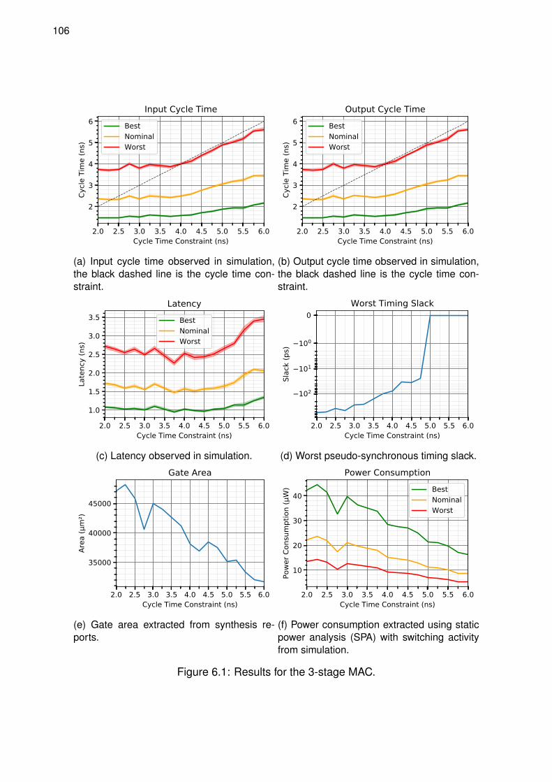
106
2.0 2.5 3.0 3.5 4.0 4.5 5.0 5.5 6.0Cycle Time Constraint (ns)
2
3
4
5
6
Cycle
Tim
e (n
s)
Input Cycle TimeBestNominalWorst
(a) Input cycle time observed in simulation,the black dashed line is the cycle time con-straint.
2.0 2.5 3.0 3.5 4.0 4.5 5.0 5.5 6.0Cycle Time Constraint (ns)
2
3
4
5
6
Cycle
Tim
e (n
s)
Output Cycle TimeBestNominalWorst
(b) Output cycle time observed in simulation,the black dashed line is the cycle time con-straint.
2.0 2.5 3.0 3.5 4.0 4.5 5.0 5.5 6.0Cycle Time Constraint (ns)
1.0
1.5
2.0
2.5
3.0
3.5
Late
ncy
(ns)
LatencyBestNominalWorst
(c) Latency observed in simulation.
2.0 2.5 3.0 3.5 4.0 4.5 5.0 5.5 6.0Cycle Time Constraint (ns)
102
101
100
0
Slac
k (p
s)
Worst Timing Slack
(d) Worst pseudo-synchronous timing slack.
2.0 2.5 3.0 3.5 4.0 4.5 5.0 5.5 6.0Cycle Time Constraint (ns)
35000
40000
45000
Area
(µm
²)
Gate Area
(e) Gate area extracted from synthesis re-ports.
2.0 2.5 3.0 3.5 4.0 4.5 5.0 5.5 6.0Cycle Time Constraint (ns)
10
20
30
40
Powe
r Con
sum
ptio
n (µ
W)
Power ConsumptionBestNominalWorst
(f) Power consumption extracted using staticpower analysis (SPA) with switching activityfrom simulation.
Figure 6.1: Results for the 3-stage MAC.

107
2.0 2.5 3.0 3.5 4.0 4.5 5.0 5.5 6.0Cycle Time Constraint (ns)
1
2
3
4
5
6
Cycle
Tim
e (n
s)
Input Cycle TimeBestNominalWorst
(a) Input cycle time observed in simulation.The black dashed line is the cycle time con-straint.
2.0 2.5 3.0 3.5 4.0 4.5 5.0 5.5 6.0Cycle Time Constraint (ns)
1
2
3
4
5
6
Cycle
Tim
e (n
s)
Output Cycle TimeBestNominalWorst
(b) Output cycle time observed in simulation.The black dashed line is the cycle time con-straint.
2.0 2.5 3.0 3.5 4.0 4.5 5.0 5.5 6.0Cycle Time Constraint (ns)
1
2
3
4
5
Late
ncy
(ns)
LatencyBestNominalWorst
(c) Latency observed in simulation.
2.0 2.5 3.0 3.5 4.0 4.5 5.0 5.5 6.0Cycle Time Constraint (ns)
102
101
100
0
Slac
k (p
s)
Worst Timing Slack
(d) Worst pseudo-synchronous timing slack.
2.0 2.5 3.0 3.5 4.0 4.5 5.0 5.5 6.0Cycle Time Constraint (ns)
35000
40000
45000
50000
55000
Area
(µm
²)
Gate Area
(e) Gate area extracted from synthesis re-ports.
2.0 2.5 3.0 3.5 4.0 4.5 5.0 5.5 6.0Cycle Time Constraint (ns)
10
20
30
40
50
60
Powe
r Con
sum
ptio
n (µ
W)
Power ConsumptionBestNominalWorst
(f) Power consumption extracted using staticpower analysis (SPA) with switching activityfrom simulation.
Figure 6.2: Results for the 4-stage MAC.
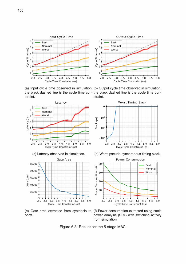
108
2.0 2.5 3.0 3.5 4.0 4.5 5.0 5.5 6.0Cycle Time Constraint (ns)
1
2
3
4
5
6
Cycle
Tim
e (n
s)
Input Cycle TimeBestNominalWorst
(a) Input cycle time observed in simulation,the black dashed line is the cycle time con-straint.
2.0 2.5 3.0 3.5 4.0 4.5 5.0 5.5 6.0Cycle Time Constraint (ns)
1
2
3
4
5
6
Cycle
Tim
e (n
s)
Output Cycle TimeBestNominalWorst
(b) Output cycle time observed in simulation,the black dashed line is the cycle time con-straint.
2.0 2.5 3.0 3.5 4.0 4.5 5.0 5.5 6.0Cycle Time Constraint (ns)
1
2
3
4
5
6
Late
ncy
(ns)
LatencyBestNominalWorst
(c) Latency observed in simulation.
2.0 2.5 3.0 3.5 4.0 4.5 5.0 5.5 6.0Cycle Time Constraint (ns)
102
101
100
0
Slac
k (p
s)
Worst Timing Slack
(d) Worst pseudo-synchronous timing slack.
2.0 2.5 3.0 3.5 4.0 4.5 5.0 5.5 6.0Cycle Time Constraint (ns)
35000
40000
45000
50000
55000
Area
(µm
²)
Gate Area
(e) Gate area extracted from synthesis re-ports.
2.0 2.5 3.0 3.5 4.0 4.5 5.0 5.5 6.0Cycle Time Constraint (ns)
20
40
60
80
Powe
r Con
sum
ptio
n (µ
W)
Power ConsumptionBestNominalWorst
(f) Power consumption extracted using staticpower analysis (SPA) with switching activityfrom simulation.
Figure 6.3: Results for the 5-stage MAC.

109
2.0 2.5 3.0 3.5 4.0 4.5 5.0 5.5 6.0Cycle Time Constraint (ns)
1
2
3
4
5
6
Cycle
Tim
e (n
s)
Input Cycle TimeBestNominalWorst
(a) Input cycle time observed in simulation.The black dashed line is the cycle time con-straint.
2.0 2.5 3.0 3.5 4.0 4.5 5.0 5.5 6.0Cycle Time Constraint (ns)
1
2
3
4
5
6
Cycle
Tim
e (n
s)
Output Cycle TimeBestNominalWorst
(b) Output cycle time observed in simulation,The black dashed line is the cycle time con-straint.
2.0 2.5 3.0 3.5 4.0 4.5 5.0 5.5 6.0Cycle Time Constraint (ns)
2
4
6
8
Late
ncy
(ns)
LatencyBestNominalWorst
(c) Latency observed in simulation.
2.0 2.5 3.0 3.5 4.0 4.5 5.0 5.5 6.0Cycle Time Constraint (ns)
102
101
100
0
Slac
k (p
s)
Worst Timing Slack
(d) Worst pseudo-synchronous timing slack.
2.0 2.5 3.0 3.5 4.0 4.5 5.0 5.5 6.0Cycle Time Constraint (ns)
35000
40000
45000
50000
55000
60000
Area
(µm
²)
Gate Area
(e) Gate area extracted from synthesis re-ports.
2.0 2.5 3.0 3.5 4.0 4.5 5.0 5.5 6.0Cycle Time Constraint (ns)
20
40
60
80
100
Powe
r Con
sum
ptio
n (µ
W)
Power ConsumptionBestNominalWorst
(f) Power consumption extracted using staticpower analysis (SPA) with switching activityfrom simulation.
Figure 6.4: Results for the 6-stage MAC.

110
2.0 2.5 3.0 3.5 4.0 4.5 5.0 5.5 6.0Cycle Time Constraint (ns)
1
2
3
4
5
6
Cycle
Tim
e (n
s)
Input Cycle TimeBestNominalWorst
(a) Input cycle time observed in simulation.The black dashed line is the cycle time con-straint.
2.0 2.5 3.0 3.5 4.0 4.5 5.0 5.5 6.0Cycle Time Constraint (ns)
1
2
3
4
5
6
Cycle
Tim
e (n
s)
Output Cycle TimeBestNominalWorst
(b) Output cycle time observed in simulation.The black dashed line is the cycle time con-straint.
2.0 2.5 3.0 3.5 4.0 4.5 5.0 5.5 6.0Cycle Time Constraint (ns)
2
4
6
8
Late
ncy
(ns)
LatencyBestNominalWorst
(c) Latency observed in simulation.
2.0 2.5 3.0 3.5 4.0 4.5 5.0 5.5 6.0Cycle Time Constraint (ns)
102
101
100
0
100
Slac
k (p
s)Worst Timing Slack
(d) Worst pseudo-synchronous timing slack.
2.0 2.5 3.0 3.5 4.0 4.5 5.0 5.5 6.0Cycle Time Constraint (ns)
35000
40000
45000
50000
55000
Area
(µm
²)
Gate Area
(e) Gate area extracted from synthesis re-ports.
2.0 2.5 3.0 3.5 4.0 4.5 5.0 5.5 6.0Cycle Time Constraint (ns)
20
40
60
80
Powe
r Con
sum
ptio
n (µ
W)
Power ConsumptionBestNominalWorst
(f) Power consumption extracted using staticpower analysis (SPA) with switching activityfrom simulation.
Figure 6.5: Results for the 6-stage MAC synthesised with timing path exceptions on free-slack.

111
7. CONCLUSION AND FUTURE WORK
This Dissertation has presented Pulsar, a innovative synthesis flow for QDI circuits.Pulsar leverages commercial EDA tools for the design capture, dual-rail expansion, technol-ogy mapping and optimisation of QDI circuits. It also enables the sign-off of target cycletimes for QDI circuits using commercial EDA tools. This is a major breakthrough for QDIdesigners, as they can now safely bound worst case performance metrics for their targetapplications. Moreover, the flow enables designers to naturally trade performance, powerand area optimisations, whenever there is slack in timing budgets.
The use of commercial EDA tools facilitates its adoption and integration in indus-trial flows. First, Pulsar uses an RTL-like description for design capture, a description formfamiliar to most designers. In this aspect, Pulsar is very similar to Uncle [RST12], whereasboth synthesise single-rail netlists that are latter expanded to a QDI circuit. The approachproposed here allows the use of commercial tools optimisation and retiming algorithms forlogic, data-path, state machine synthesis. However, RTL descriptions are not fully ade-quate for capturing the behaviour of asynchronous circuits. They often rely on the globalclock signal to synchronise the merging of data flows, making it not suitable to capture theinter-dependencies of data flows in the circuit. A common and well established approach isto use descriptions based on Hoare communicating sequential processes (CSP) [Hoa85].For instance, Concurrent Hardware Processes (CHP) [MM11], based on CSP, is used fordesign capture in Beerel et al. Proteus [BDL11], Manohar ACT [Man19] and others. An-other classical CSP-based language is Balsa [EB02], which has its own synthesis tool, butit is also used as a language on Teak [BTE09]. Another interesting approach is the useof functional programming languages, this is explored for synchronous circuits on workssuch as Lava [BCSS99, Gil11], CλasH (pronounced Clash) [BKK+10] and Chisel [BVR+12].Also, the current design capture and dual-rail expansion technique is limited to deterministicpipelines, which limits the application of Pulsar to more complex circuits. Future work com-prises exploring alternative design capture methodologies that better capture the behaviourof a broader range of asynchronous circuits.
The use of standard EDA also tools helps integrating QDI circuits in existing de-sign flows. This makes Pulsar attractive for designing globally asynchronous locally syn-chronous (GALS) circuits. A GALS configuration consists of synchronous circuits interfacingwith an asynchronous circuit. A GALS circuit uses an asynchronous circuit to overcome thelimitations of clock distribution on synchronous circuits. It enables different modules in acircuit to operate with different clocks with possible distinct frequencies and/or phases. Anasynchronous circuit acts as a interconnection between different circuit modules. For opti-mal performance, such an asynchronous circuit must withstand the throughput of the syn-chronous modules. A synchronous circuit throughput is dictated by its clock frequency. The
112
HBCN and the cycle time constraining methodology presented in this Dissertation enablesthe construction of QDI circuits with bounded throughput, thus enabling the construction ofinterconnection circuits for GALS design, which are capable of handling the required designthroughput.
The cycle time constraining technique presented here uses a pseudo-clock to con-strain the cycle time. This assumes that the logic of every pipeline stage has the samedelay. This assumption is only true if the pipeline is well balanced, as it disregards the logiccomplexity of individual pipeline stages. Furthermore, it also disregards the delay disparitybetween forward and backward propagation paths. In this work, empty propagation pathsinternal to the full-buffer component expansion are attributed a fixed minimal delay. Futurework will target the automatic identification of pipeline disparities and constraining of eachpropagation path in accordance to their respective logic complexity.
Another aspect of the Pulsar flow where further optimisations are expected to bebeneficial is the dual-rail expansion. Currently the dual-rail expansion relies on EDA toolsability to optimise combinations of virtual functions. However, commercial EDA tools donot recognise optimisation opportunities inherent to the use of DI codes. For instance, DIcodes expressed in binary contain a large amount of invalid binary combinations, whichcan used as "don’t-cares" during logic optimisation and technology mapping. Fant [FB96]has demonstrated that when composing image functions, which are analogous to the virtualfunctions defined in this work, minterms containing these invalid codes do arise. This opensopportunities for exploring alternative dual-rail expansion and optimisations and technologymapping techniques that take advantage of specific characteristics of DI codes. Anotheroptimisation that could be explored during the dual-rail expansion and technology mappingis relaxation [LM09]. This technique allows producing faster and smaller QDI circuits by en-abling parts of the circuit to violate the indication principle locally, while globally maintainingstrong indication. Future work will explore the construction of an alternative dual-rail expan-sion technique and possibly a technology mapper to allow these and other optimisations.
The physical synthesis, albeit possible with the current flow requires further ex-ploration. This is especially interesting when it comes to the introduction of adversarialpaths [KKM09] that hinder the indication principle. Currently, this is verified through simula-tion. However, a formal methodology for detecting these paths is highly desirable. Such amethodology would possibly not only detect potential hazards, but could also enable avoid-ing them entirely, by using e.g. relative timing constraints [MS16].
Simulation and formal verification is another aspect that requires further attention.Currently, the behaviour of the synthesised circuit is not captured in the simulation of theRTL description. Also, the current flow does not allow equivalence checking between theinput RTL description, the virtual netlist and the final synthesised netlist. Solutions to allowequivalence checking and high-level simulation shall be addressed in further work.
113
REFERENCES
[BCSS99] Bjesse, P.; Claessen, K.; Sheeran, M.; Singh, S. “Lava: Hardware Design inHaskell”, ACM Special Interest Group on Programming Languages (SIGPLAN)Notices, vol. 34–1, 1999, pp. 174–184.
[BCV+05] Beigné, E.; Clermidy, F.; Vivet, P.; Clouard, A.; Renaudin, M. “An AsynchronousNoC Architecture Providing Low Latency Service and Its Multi-Level DesignFramework”. In: IEEE International Symposium on Advanced Research inAsynchronous Circuits and Systems (ASYNC), 2005, pp. 54–63.
[BDL11] Beerel, P. A.; Dimou, G. D.; Lines, A. M. “Proteus: An ASIC Flow for GHzAsynchronous Designs”, IEEE Design & Test of Computers, vol. 28–5, 2011,pp. 36–50.
[Ber93] van Berkel, K. “Handshake Circuits: An Asynchronous Architecture for VLSIProgramming”. New York, NY, USA: Cambridge University Press, 1993, 225p.
[BKK+10] Baaij, C. P. R.; Kooijman, M.; Kuper, J.; Boeijink, W. A.; Gerards, M. E. T.“CλasH: Structural Descriptions of Synchronous Hardware using Haskell”. In:EUROMICRO Conference on Digital System Design (DSD), 2010, pp. 714–721.
[BLDK06] Beerel, P. A.; Lines, A. M.; Davies, M.; Kim, N.-H. K. “Slack MatchingAsynchronous Designs”. In: IEEE International Symposium on AdvancedResearch in Asynchronous Circuits and Systems (ASYNC), 2006, pp. 184–194.
[BOF10] Beerel, P. A.; Ozdag, R. O.; Ferretti, M. “A Designer´s Guide to AsynchronousVLSI”. Cambridge University Press, 2010, 353p.
[BSVMH84] Brayton, R. K.; Sangiovanni-Vincentelli, A.; McMullen, C.; Hachtel, G. “LogicMinimization Algorithms for VLSI Synthesis”. Norwell, MA, USA: KluwerAcademic Publishers, 1984, 174p.
[BTE09] Bardsley, A.; Tarazona, L.; Edwards, D. “Teak: A Token-Flow Implementation forthe Balsa Language”. In: 2009 Ninth International Conference on Applicationof Concurrency to System Design, 2009, pp. 23–31.
[BVR+12] Bachrach, J.; Vo, H.; Richards, B.; Lee, Y.; Waterman, A.; Avižienis, R.;Wawrzynek, J.; Asanovic, K. “Chisel: Constructing hardware in a Scalaembedded language”. In: Design Automation Conference (DAC), 2012, pp.1212–1221.

114
[CCGC10] Chen, J.; Chong, K.-S.; Gwee, B.-H.; Chang, J. S. “An ultra-low powerasynchronous quasi-delay-insensitive (QDI) sub-threshold memory with bit-interleaving and completion detection”. In: 8th IEEE International NEWCASConference (NEWCAS), 2010, pp. 117–120.
[CLRS09] Cormen, T. H.; Leiserson, C. E.; Rivest, R. L.; Stein, C. “Introduction toAlgorithms”. The MIT Press, 2009, 3rd ed., 1292p.
[DCB93] Das, D. K.; Chacraborty, S.; Bhattacharya, B. B. “Irredundant binate realizationsof unate functions”, International Journal of Electronics Theoretical andExperimental, vol. 75–1, 1993, pp. 65–73.
[DLD+14] Davies, M.; Lines, A.; Dama, J.; Gravel, A.; Southworth, R.; Dimou, G.;Beerel, P. A. “A 72-Port 10G Ethernet Switch/Router Using Quasi-Delay-Insensitive Asynchronous Design”. In: 20th IEEE International Symposium onAsynchronous Circuits and Systems (ASYNC), 2014, pp. 103–104.
[DMM04] Donno, M.; Macii, E.; Mazzoni, L. “Power-aware clock tree planning”. In:International Symposium on Physical Design (ISPD), 2004, pp. 138–147.
[EB02] Edwards, D.; Bardsley, A. “Balsa: An Asynchronous Hardware SynthesisLanguage”, The Computer Journal, vol. 45–1, 2002, pp. 12–18.
[Fan05] Fant, K. M. “Logically Determined Design: Clockless System Design with NULLConvention Logic”. Wiley, 2005, 292p.
[FB96] Fant, K. M.; Brandt, S. A. “NULL Convention LogicTM : A complete andconsistent logic for asynchronous digital circuit synthesis”. In: InternationalConference on Application Specific Systems, Architectures and Processors(ASAP), 1996, pp. 261–273.
[Fre12] Free Software Foundation, Inc. “GNU Linear Programming Kit (GLPK)”.Source: https://www.gnu.org/software/glpk/glpk.html, 2012.
[Gil11] Gill, A. “Declarative FPGA Circuit Synthesis using Kansas Lava”. In:International Conference on Engineering of Reconfigurable Systems andAlgorithms (ERSA), 2011, pp. 55–64.
[GLY10] Guan, X.; Liu, Y.; Yang, Y. “Performance Analysis of Low Power Null ConventionLogic Units with Power Cutoff”. In: Asia-Pacific Conference on WearableComputing Systems (APWCS), 2010, pp. 55–58.
[Har01] Harris, D. “Skew-tolerant Circuit Design”. Morgan Kaufmann, 2001, 300p.
[Hoa78] Hoare, C. A. R. “Communicating Sequential Processes”, Communications ofthe ACM, vol. 21–8, Aug 1978, pp. 666–677.

115
[Hoa85] Hoare, C. A. R. “Communicating Sequential Processes”. Prentice HallInternational, 1985, 260p.
[Hur69] Hurst, S. “An Introduction to Threshold Logic: A survey of present theory andpractice”, The Radio and Electronic Engineer, vol. 37–6, 1969, pp. 339–351.
[JN08] Jeong, C.; Nowick, S. “Technology Mapping and Cell Merger for AsynchronousThreshold Networks”, IEEE Transactions on Computer-Aided Design ofIntegrated Circuits and Systems, vol. 27–4, 2008, pp. 659–672.
[JSL+10] Jorgenson, R.; Sorensen, L.; Leet, D.; Hagedorn, M.; Lamb, D.; Friddell,T.; Snapp, W. “Ultralow-Power Operation in Subthreshold Regimes ApplyingClockless Logic”, Proceedings of the IEEE, vol. 98–2, Feb 2010, pp. 299–314.
[KKM09] Keller, S.; Katelman, M.; Martin, A. J. “A Necessary and SufficientTiming Assumption for Speed-Independent Circuits”. In: IEEE InternationalSymposium on Advanced Research in Asynchronous Circuits and Systems(ASYNC), 2009, pp. 65–76.
[LM09] LaFrieda, C.; Manohar, R. “Reducing Power Consumption with Relaxed QuasiDelay-Insensitive Circuits”. In: IEEE International Symposium on AdvancedResearch in Asynchronous Circuits and Systems (ASYNC), 2009, pp. 217–226.
[Mag84] Magott, J. “Performance Evaluation of Concurrent Systems using Petri Nets”,Information Processing Letters, vol. 18–1, 1984, pp. 7–13.
[Man19] Manohar, R. “An Open-Source Design Flow for Asynchronous Circuits”. In:Government Microcircuit Applications And Critical Technology Conference(GOMACTECH), 2019, pp. 1–5.
[MBSC18] Moreira, M, T.; Beerel, P. A.; Sartori, M. L. L.; Calazans, N. L. V. “NCL SynthesisWith Conventional EDA Tools: Technology Mapping and Optimization”, IEEETransactions on Circuits and Systems I: Regular Papers, vol. 65–6, 2018, pp.1981–1993.
[MGC12] Moreira, M. T.; Guazzelli, R. A.; Calazans, N. L. V. “Return-to-One Protocolfor Reducing Static Power in QDI Circuits Employing m-of-n Codes”. In:Symposium on Integrated Circuits and Systems Design (SBCCI), 2012, pp.1–6.
[MGHC14] Moreira, M. T.; Guazzelli, R. A.; Heck, G.; Calazans, N. L. V. “Hardening QDICircuits Against Transient Faults Using Delay-Insensitive Maxterm Synthesis”.In: ACM Great Lakes Symposium on VLSI (GLSVLSI), 2014, pp. 3–8.
116
[MM11] Martin, A. J.; Moore, C. D. “CHP and CHPsim: A Language and Simulatorfor Fine-grain Distributed Computation”, Technical Report, CS Dept., Caltech,Pasadena, CA, USA, Tech. Rep. CS-TR-1-2011, 2011, 12p.
[MN06] Martin, A.; Nyström, M. “Asynchronous Techniques for System-on-ChipDesign”, Proceedings of the IEEE, vol. 94–6, Jun 2006, pp. 1089–1120.
[MNM+14] Moreira, M. T.; Neutzling, A.; Martins, M.; Reis, A.; Ribas, R.; Calazans, N. L. V.“Semi-custom NCL Design with Commercial EDA Frameworks: Is it possible?”In: IEEE International Symposium on Advanced Research in AsynchronousCircuits and Systems (ASYNC), 2014, pp. 53–60.
[MNW03] Martin, A. J.; Nyström, M.; Wong, C. G. “Three Generations of AsynchronousMicroprocessors”, IEEE Design & Test of Computers, vol. 20–6, 2003, pp. 9–17.
[MOPC11] Moreira, M. T.; Oliveira, B. S.; Pontes, J. J. H.; Calazans, N. L. V. “A 65nmStandard Cell Set and Flow Dedicated to Automated Asynchronous CircuitsDesign”. In: IEEE International System on Chip Conference (SoCC), 2011, pp.99–104.
[MOPC13] Moreira, M. T.; Oliveira, C. H. M.; Porto, R. C.; Calazans, N. L. V.“NCL+: Return-to-one Null Convention Logic”. In: IEEE International MidwestSymposium on Circuits and Systems (MWSCAS), 2013, pp. 836–839.
[Mor16] Moreira, M. T. “Asynchronous Circuits: Innovations in Components, CellLibraries and Design Templates”, Ph.D. Thesis, Pontifícia UniversidadeCatólica do Rio Grande do Sul, FACIN-PPGCC, 2016, 276p.
[MPC14] Moreira, M. T.; Pontes, J. H.; Calazans, N. L. V. “Tradeoffs between RTO andRTZ in WCHB QDI Asynchronous Design”. In: International Symposium onQuality Electronic Design (ISQED), 2014, pp. 692–699.
[MS16] Manoranjan, J. V.; Stevens, K. S. “Qualifying relative timing constraintsfor asynchronous circuits”. In: IEEE International Symposium on AdvancedResearch in Asynchronous Circuits and Systems (ASYNC), 2016, pp. 91–98.
[MTMC14] Moreira, M. T.; Trojan, G.; Moraes, F. G.; Calazans, N. L. V. “SpatiallyDistributed Dual-Spacer Null Convention Logic Design”, Journal of Low PowerElectronics, vol. 10–3, 2014, pp. 313–320.
[Mur89] Murata, T. “Petri nets: Properties, analysis and applications”, Proceedings ofthe IEEE, vol. 77–4, 1989, pp. 541–580.
117
[NS15a] Nowick, S. M.; Singh, M. “Asynchronous Design - Part 1: Overview and RecentAdvances”, IEEE Design & Test of Computers, vol. 32–3, Jun 2015, pp. 5–18.
[NS15b] Nowick, S. M.; Singh, M. “Asynchronous Design - Part 2: Systems andMethodologies”, IEEE Design & Test of Computers, vol. 32–3, Jun 2015, pp.19–28.
[PMMC10] Pontes, J.; Moreira, M. T.; Moraes, F. G.; Calazans, N. L. V. “Hermes-AA: A65nm asynchronous NoC router with adaptive routing”. In: IEEE InternationalSystem-on-Chip Conference (SOCC), 2010, pp. 493–498.
[PTE05] Plana, L. A.; Taylor, S.; Edwards, D. “Attacking Control Overhead to ImproveSynthesised Asynchronous Circuit Performance”. In: IEEE InternationalConference on Computer Design (ICCD), 2005, pp. 703–710.
[Rei13] Reisig, W. “Understanding Petri Nets: Modeling Techniques, Analysis Methods,Case Studies”. Springer, 2013, 230p.
[RST12] Reese, R. B.; Smith, S. C.; Thornton, M. A. “Uncle - An RTL Approachto Asynchronous Design”. In: IEEE International Symposium on AdvancedResearch in Asynchronous Circuits and Systems (ASYNC), 2012, pp. 65–72.
[SCH+11] Seok, M.; Chen, G.; Hanson, S.; Wieckowski, M.; Blaauw, D.; Sylvester,D. “Mitigating Variability in Near-Threshold Computing”, IEEE Journal onEmerging and Selected Topics in Circuits and Systems, vol. 1–1, Mar 2011,pp. 42–49.
[SDF06] Sutherland, S.; Davidmann, S.; Flake, P. “SystemVerilog for Design: A Guide toUsing SystemVerilog for Hardware Design and Modeling”. Springer Science &Business Media, 2006, 2nd ed., 418p.
[SF01] Sparsø, J.; Furber, S. “Principles of Asynchronous Circuit Design – A SystemsPerspective”. Springer, 2001, 356p.
[Sut89] Sutherland, I. E. “Micropipelines”, Communications of the ACM, vol. 32–6,Jun 1989, pp. 720–738.
[Tan18] Tange, O. “GNU Parallel 2018”. Ole Tange, 2018, 112p.
[TBV12] Thonnart, Y.; Beigné, E.; Vivet, P. “A pseudo-synchronous Implementation Flowfor WCHB QDI Asynchronous Circuits”. In: IEEE International Symposium onAdvanced Research in Asynchronous Circuits and Systems (ASYNC), 2012,pp. 73–80.
[Ver88] Verhoeff, T. “Delay-Insensitive Codes - An Overview”, Distributed Computing,vol. 3–1, Mar 1988, pp. 1–8.

118
[ZSD10] Zhou, L.; Smith, S.; Di, J. “Bit-Wise MTNCL: An ultra-low power bit-wise pipelined asynchronous circuit design methodology”. In: 53rd IEEEInternational Midwest Symposium on Circuits and Systems (MWSCAS), 2010,pp. 217–220.
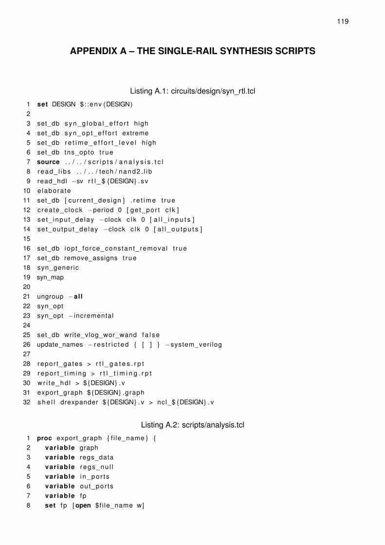
119
APPENDIX A – THE SINGLE-RAIL SYNTHESIS SCRIPTS
Listing A.1: circuits/design/syn_rtl.tcl
1 set DESIGN $: :env (DESIGN)23 set_db s y n _ g l o b a l _ e f f o r t h igh4 set_db syn_op t_e f f o r t extreme5 set_db r e t i m e _ e f f o r t _ l e v e l high6 set_db tns_opto t rue7 source . . / . . / s c r i p t s / a n a l y s i s . t c l8 read_ l i bs . . / . . / tech / nand2 . l i b9 read_hdl −sv r t l _ $ {DESIGN} .sv
10 e labora te11 set_db [ cur ren t_des ign ] . r e t i m e t rue12 crea te_c lock −period 0 [ ge t_por t c l k ]13 se t_ inpu t_de lay −clock c l k 0 [ a l l _ i n p u t s ]14 set_output_de lay −clock c l k 0 [ a l l _ o u t p u t s ]1516 set_db iop t_ fo rce_constan t_remova l t r ue17 set_db remove_assigns t rue18 syn_gener ic19 syn_map2021 ungroup −all22 syn_opt23 syn_opt − incremental2425 set_db write_vlog_wor_wand f a l s e26 update_names − r e s t r i c t e d { [ ] } −system_veri log2728 repor t_ga tes > r t l _ g a t e s . r p t29 r e p o r t _ t i m i n g > r t l _ t i m i n g . r p t30 w r i t e_ h d l > $ {DESIGN} . v31 export_graph $ {DESIGN} .graph32 s h e l l drexpander $ {DESIGN} . v > ncl_$ {DESIGN} . v
Listing A.2: scripts/analysis.tcl
1 proc export_graph { f i le_name } {2 var iable graph3 var iable regs_data4 var iable r egs_nu l l5 var iable i n_po r t s6 var iable out_por ts7 var iable fp8 set fp [ open $f i le_name w]
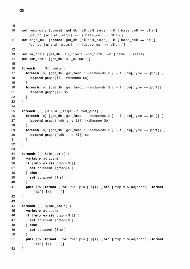
120
910 set regs_data [ concat [ get_db [ a l l : : a l l _ s e q s ] − i f { . base_ce l l == d f f r } ]
[ get_db [ a l l : : a l l _ s e q s ] − i f { . base_ce l l == d f f s } ] ]11 set r egs_nu l l [ concat [ get_db [ a l l : : a l l _ s e q s ] − i f { . base_ce l l == d f f } ]
[ get_db [ a l l : : a l l _ s e q s ] − i f { . base_ce l l == d f fen } ] ]1213 set i n_po r t s [ get_db [ a l l _ i n p u t s −no_clock ] − i f { .name ! = rese t } ]14 set out_por ts [ get_db [ a l l _ o u t p u t s ] ]1516 foreach { i } $ in_por ts {17 foreach { o } [ get_db [ get_ fanout −endpoints $ i ] − i f { . ob j_ t ype == pin } ] {18 lappend graph ( $ i ) [ vdirname $o ]19 }20 foreach { o } [ get_db [ get_ fanout −endpoints $ i ] − i f { . ob j_ t ype == po r t } ] {21 lappend graph ( $ i ) $o22 }23 }2425 foreach { i } [ a l l : : a l l _ s e q s −output_pins ] {26 foreach { o } [ get_db [ get_ fanout −endpoints $ i ] − i f { . ob j_ t ype == pin } ] {27 lappend graph ( [ vdirname $ i ] ) [ vdirname $o ]28 }29 foreach { o } [ get_db [ get_ fanout −endpoints $ i ] − i f { . ob j_ t ype == po r t } ] {30 lappend graph ( [ vdirname $ i ] ) $o31 }32 }3334 foreach { i } $ { i n_po r t s } {35 var iable adjacent36 i f [ info exists graph ( $ i ) ] {37 set adjacent $graph ( $ i )38 } else {39 set adjacent [ l i s t ]40 }41 puts $fp [ format { Por t "%s " [%s ] } $ { i } [ jo in [ lmap x $ { ad jacent } { format
{ "%s " } $x } ] { , } ] ]42 }4344 foreach { i } $ { ou t_por ts } {45 var iable adjacent46 i f [ info exists graph ( $ i ) ] {47 set adjacent $graph ( $ i )48 } else {49 set adjacent [ l i s t ]50 }51 puts $fp [ format { Por t "%s " [%s ] } $ { i } [ jo in [ lmap x $ { ad jacent } { format
{ "%s " } $x } ] { , } ] ]52 }

121
5354 foreach { i } $ { regs_data } {55 var iable adjacent56 i f [ info exists graph ( $ i ) ] {57 set adjacent $graph ( $ i )58 } else {59 set adjacent [ l i s t ]60 }61 puts $fp [ format { DataReg "%s " [%s ] } $ { i } [ jo in [ lmap x $ { ad jacent } { format
{ "%s " } $x } ] { , } ] ]62 }6364 foreach { i } $ { regs_nu l l } {65 var iable adjacent66 i f [ info exists graph ( $ i ) ] {67 set adjacent $graph ( $ i )68 } else {69 set adjacent [ l i s t ]70 }71 puts $fp [ format { NullReg "%s " [%s ] } $ { i } [ jo in [ lmap x $ { ad jacent } { format
{ "%s " } $x } ] { , } ] ]72 }7374 close $fp75 unset −nocomplain graph76 unset −nocomplain regs_data77 unset −nocomplain regs_nu l l78 unset −nocomplain i n_po r t s79 unset −nocomplain ou t_por ts80 }8182 # Local V a r i a b l e s :83 # t c l− i n d e n t− l e v e l : 284 # indent−tabs−mode: n i l85 # End:
Listing A.3: tech/nand2.lib – The component library Liberty file.
1 l i b r a r y (PULSAR_NAND2) {2 delay_model : tab le_ lookup ;345 / * u n i t a t t r i b u t e s * /6 t ime_un i t : " 1ns " ;7 vo l t a ge_un i t : " 1V" ;8 c u r r e n t _ u n i t : " 1mA" ;9 p u l l i n g _ r e s i s t a n c e _ u n i t : " 1kohm" ;
10 leakage_power_unit : " 1pW" ;

122
11 c a p a c i t i v e _ l o a d _ u n i t ( 1 . 0 , p f ) ;1213 / * opera t ion cond i t i ons * /14 nom_process : 1 ;15 nom_temperature : 25;16 nom_voltage : 1 . 2 ;17 opera t i ng_cond i t i ons ( t y p i c a l ) {18 process : 1 ;19 temperature : 25;20 vo l tage : 1 . 2 ;21 t ree_ type : balanced_tree22 }23 de fau l t _ope ra t i ng_cond i t i ons : t y p i c a l ;2425 / * th resho ld d e f i n i t i o n s * /26 s lew_ lower_ th resho ld_pc t_ fa l l : 30 .0 ;27 s lew_upper_ th resho ld_pc t_ fa l l : 70 .0 ;28 s lew_ lower_ th resho ld_pc t_ r i se : 30 .0 ;29 s lew_upper_ thresho ld_pct_r ise : 70 .0 ;30 i n p u t _ t h r e s h o l d _ p c t _ f a l l : 50 .0 ;31 i n p u t _ t h r e s h o l d _ p c t _ r i s e : 50 .0 ;32 o u t p u t _ t h r e s h o l d _ p c t _ f a l l : 50 .0 ;33 ou tpu t_ th resho ld_pc t_ r i se : 50 .0 ;34 s lew_dera te_ f rom_ l ib ra ry : 0 . 5 ;3536 / * d e f a u l t a t t r i b u t e s * /37 defaul t_ leakage_power_densi ty : 0 . 0 ;38 defau l t_ce l l_ leakage_power : 0 . 0 ;39 de fau l t_ fanou t_ load : 1 . 0 ;40 defau l t_ou tpu t_p in_cap : 0 . 0 ;41 de fau l t_ inou t_p in_cap : 0.00158;42 de fau l t_ inpu t_p in_cap : 0.00158;43 de fau l t _max_ t rans i t i on : 1 .02 ;444546 c e l l ( nor2 ) {47 area : 31 .0 ;48 p in ( a ) {49 d i r e c t i o n : i npu t ;50 capaci tance : 0 .002;51 }52 p in ( b ) {53 d i r e c t i o n : i npu t ;54 capaci tance : 0 .002;55 }56 p in ( y ) {57 d i r e c t i o n : output ;58 capaci tance : 0 . 0 ;
123
59 f u n c t i o n : " ! ( a | b ) " ;60 t im ing ( ) {61 re l a ted_p in : " a " ;62 t iming_sense : negat ive_unate ;63 c e l l _ r i s e ( sca la r ) {64 values ( " 0.01 " ) ;65 }66 r i s e _ t r a n s i t i o n ( sca la r ) {67 values ( " 0.0 " ) ;68 }69 c e l l _ f a l l ( sca la r ) {70 values ( " 0.02 " ) ;71 }72 f a l l _ t r a n s i t i o n ( sca la r ) {73 values ( " 0.0 " ) ;74 }75 }76 t im ing ( ) {77 re l a ted_p in : " b " ;78 t iming_sense : negat ive_unate ;79 c e l l _ r i s e ( sca la r ) {80 values ( " 0.01 " ) ;81 }82 r i s e _ t r a n s i t i o n ( sca la r ) {83 values ( " 0.0 " ) ;84 }85 c e l l _ f a l l ( sca la r ) {86 values ( " 0.02 " ) ;87 }88 f a l l _ t r a n s i t i o n ( sca la r ) {89 values ( " 0.0 " ) ;90 }91 }92 }93 }9495 c e l l ( nand2 ) {96 area : 31 .0 ;97 p in ( a ) {98 d i r e c t i o n : i npu t ;99 capaci tance : 0 .002;
100 }101 p in ( b ) {102 d i r e c t i o n : i npu t ;103 capaci tance : 0 .002;104 }105 p in ( y ) {106 d i r e c t i o n : output ;

124
107 capaci tance : 0 . 0 ;108 f u n c t i o n : " ! ( a *b ) " ;109 t im ing ( ) {110 re l a ted_p in : " a " ;111 t iming_sense : negat ive_unate ;112 c e l l _ r i s e ( sca la r ) {113 values ( " 0.02 " ) ;114 }115 r i s e _ t r a n s i t i o n ( sca la r ) {116 values ( " 0.0 " ) ;117 }118 c e l l _ f a l l ( sca la r ) {119 values ( " 0.01 " ) ;120 }121 f a l l _ t r a n s i t i o n ( sca la r ) {122 values ( " 0.0 " ) ;123 }124 }125 t im ing ( ) {126 re l a ted_p in : " b " ;127 t iming_sense : negat ive_unate ;128 c e l l _ r i s e ( sca la r ) {129 values ( " 0.02 " ) ;130 }131 r i s e _ t r a n s i t i o n ( sca la r ) {132 values ( " 0.0 " ) ;133 }134 c e l l _ f a l l ( sca la r ) {135 values ( " 0.01 " ) ;136 }137 f a l l _ t r a n s i t i o n ( sca la r ) {138 values ( " 0.0 " ) ;139 }140 }141 }142 }143144 c e l l ( i nv ) {145 area : 1 . 0 ;146 p in ( a ) {147 d i r e c t i o n : i npu t ;148 capaci tance : 0 .001;149 }150 p in ( y ) {151 d i r e c t i o n : output ;152 capaci tance : 0 . 0 ;153 f u n c t i o n : " ! a " ;154 t im ing ( ) {
125
155 re l a ted_p in : " a " ;156 t iming_sense : negat ive_unate ;157 c e l l _ r i s e ( sca la r ) {158 values ( " 0.0 " ) ;159 }160 r i s e _ t r a n s i t i o n ( sca la r ) {161 values ( " 0.0 " ) ;162 }163 c e l l _ f a l l ( sca la r ) {164 values ( " 0.0 " ) ;165 }166 f a l l _ t r a n s i t i o n ( sca la r ) {167 values ( " 0.0 " ) ;168 }169 }170 }171 }172173 c e l l ( b u f f ) {174 area : 1 . 0 ;175 p in ( a ) {176 d i r e c t i o n : i npu t ;177 capaci tance : 0 .001;178 }179 p in ( y ) {180 d i r e c t i o n : output ;181 capaci tance : 0 . 0 ;182 f u n c t i o n : " a " ;183 t im ing ( ) {184 re l a ted_p in : " a " ;185 t iming_sense : pos i t i ve_una te ;186 c e l l _ r i s e ( sca la r ) {187 values ( " 0.0 " ) ;188 }189 r i s e _ t r a n s i t i o n ( sca la r ) {190 values ( " 0.0 " ) ;191 }192 c e l l _ f a l l ( sca la r ) {193 values ( " 0.0 " ) ;194 }195 f a l l _ t r a n s i t i o n ( sca la r ) {196 values ( " 0.0 " ) ;197 }198 }199 }200 }201202 c e l l ( xor2 ) {

126
203 area : 38 .0 ;204 p in ( a ) {205 d i r e c t i o n : i npu t ;206 capaci tance : 0 .002;207 }208 p in ( b ) {209 d i r e c t i o n : i npu t ;210 capaci tance : 0 .002;211 }212 p in ( y ) {213 d i r e c t i o n : output ;214 capaci tance : 0 . 0 ;215 f u n c t i o n : " a^b " ;216 t im ing ( ) {217 re l a ted_p in : " a " ;218 t iming_sense : pos i t i ve_una te ;219 c e l l _ r i s e ( sca la r ) {220 values ( " 0.015 " ) ;221 }222 r i s e _ t r a n s i t i o n ( sca la r ) {223 values ( " 0.0 " ) ;224 }225 c e l l _ f a l l ( sca la r ) {226 values ( " 0.015 " ) ;227 }228 f a l l _ t r a n s i t i o n ( sca la r ) {229 values ( " 0.0 " ) ;230 }231 }232 t im ing ( ) {233 re l a ted_p in : " b " ;234 t iming_sense : pos i t i ve_una te ;235 c e l l _ r i s e ( sca la r ) {236 values ( " 0.015 " ) ;237 }238 r i s e _ t r a n s i t i o n ( sca la r ) {239 values ( " 0.0 " ) ;240 }241 c e l l _ f a l l ( sca la r ) {242 values ( " 0.015 " ) ;243 }244 f a l l _ t r a n s i t i o n ( sca la r ) {245 values ( " 0.0 " ) ;246 }247 }248 t im ing ( ) {249 re l a ted_p in : " a " ;250 t iming_sense : negat ive_unate ;

127
251 c e l l _ r i s e ( sca la r ) {252 values ( " 0.015 " ) ;253 }254 r i s e _ t r a n s i t i o n ( sca la r ) {255 values ( " 0.0 " ) ;256 }257 c e l l _ f a l l ( sca la r ) {258 values ( " 0.015 " ) ;259 }260 f a l l _ t r a n s i t i o n ( sca la r ) {261 values ( " 0.0 " ) ;262 }263 }264 t im ing ( ) {265 re l a ted_p in : " b " ;266 t iming_sense : negat ive_unate ;267 c e l l _ r i s e ( sca la r ) {268 values ( " 0.015 " ) ;269 }270 r i s e _ t r a n s i t i o n ( sca la r ) {271 values ( " 0.0 " ) ;272 }273 c e l l _ f a l l ( sca la r ) {274 values ( " 0.015 " ) ;275 }276 f a l l _ t r a n s i t i o n ( sca la r ) {277 values ( " 0.0 " ) ;278 }279 }280 }281 }282283 c e l l ( d f f ) {284 area : 32 .0 ;285 p in ( d ) {286 d i r e c t i o n : i npu t ;287 capaci tance : 0 .001;288 t im ing ( ) {289 re l a ted_p in : " ck " ;290 t im ing_ type : se tup_ r i s i ng ;291 r i s e _ c o n s t r a i n t ( sca la r ) {292 values ( " 0.0 " ) ;293 }294 f a l l _ c o n s t r a i n t ( sca la r ) {295 values ( " 0.0 " ) ;296 }297 }298 t im ing ( ) {

128
299 re l a ted_p in : " ck " ;300 t im ing_ type : h o l d _ r i s i n g ;301 r i s e _ c o n s t r a i n t ( sca la r ) {302 values ( " 0.0 " ) ;303 }304 f a l l _ c o n s t r a i n t ( sca la r ) {305 values ( " 0.0 " ) ;306 }307 }308 }309 p in ( ck ) {310 d i r e c t i o n : i npu t ;311 c lock : t r ue ;312 capaci tance : 0 .001;313 }314 f f ( IQ , IQN) {315 clocked_on : " ck " ;316 nex t_s ta te : " d " ;317 }318 p in ( q ) {319 d i r e c t i o n : output ;320 capaci tance : 0 . 0 ;321 f u n c t i o n : " IQ " ;322 t im ing ( ) {323 re l a ted_p in : " ck " ;324 t im ing_ type : r is ing_edge ;325 t iming_sense : non_unate ;326 c e l l _ r i s e ( sca la r ) {327 values ( " 0.01 " ) ;328 }329 r i s e _ t r a n s i t i o n ( sca la r ) {330 values ( " 0.0 " ) ;331 }332 c e l l _ f a l l ( sca la r ) {333 values ( " 0.01 " ) ;334 }335 f a l l _ t r a n s i t i o n ( sca la r ) {336 values ( " 0.0 " ) ;337 }338 }339 }340 }341342 c e l l ( d f f r ) {343 area : 64 .0 ;344 p in ( d ) {345 d i r e c t i o n : i npu t ;346 capaci tance : 0 .001;

129
347 t im ing ( ) {348 re l a ted_p in : " ck " ;349 t im ing_ type : se tup_ r i s i ng ;350 r i s e _ c o n s t r a i n t ( sca la r ) {351 values ( " 0.0 " ) ;352 }353 f a l l _ c o n s t r a i n t ( sca la r ) {354 values ( " 0.0 " ) ;355 }356 }357 t im ing ( ) {358 re l a ted_p in : " ck " ;359 t im ing_ type : h o l d _ r i s i n g ;360 r i s e _ c o n s t r a i n t ( sca la r ) {361 values ( " 0.0 " ) ;362 }363 f a l l _ c o n s t r a i n t ( sca la r ) {364 values ( " 0.0 " ) ;365 }366 }367 }368 p in ( ck ) {369 d i r e c t i o n : i npu t ;370 c lock : t r ue ;371 capaci tance : 0 .001;372 }373 p in ( rb ) {374 d i r e c t i o n : i npu t ;375 capaci tance : 0 .001;376 t im ing ( ) {377 re l a ted_p in : " ck " ;378 t im ing_ type : se tup_ r i s i ng ;379 r i s e _ c o n s t r a i n t ( sca la r ) {380 values ( " 0.0 " ) ;381 }382 f a l l _ c o n s t r a i n t ( sca la r ) {383 values ( " 0.0 " ) ;384 }385 }386 t im ing ( ) {387 re l a ted_p in : " ck " ;388 t im ing_ type : h o l d _ r i s i n g ;389 r i s e _ c o n s t r a i n t ( sca la r ) {390 values ( " 0.0 " ) ;391 }392 f a l l _ c o n s t r a i n t ( sca la r ) {393 values ( " 0.0 " ) ;394 }

130
395 }396 }397 f f ( IQ , IQN) {398 clocked_on : " ck " ;399 nex t_s ta te : " d " ;400 c l ea r : " ( ! rb ) " ;401 }402 p in ( q ) {403 d i r e c t i o n : output ;404 capaci tance : 0 . 0 ;405 f u n c t i o n : " IQ " ;406 t im ing ( ) {407 re l a ted_p in : " ck " ;408 t im ing_ type : r is ing_edge ;409 t iming_sense : non_unate ;410 c e l l _ r i s e ( sca la r ) {411 values ( " 0.01 " ) ;412 }413 r i s e _ t r a n s i t i o n ( sca la r ) {414 values ( " 0.0 " ) ;415 }416 c e l l _ f a l l ( sca la r ) {417 values ( " 0.01 " ) ;418 }419 f a l l _ t r a n s i t i o n ( sca la r ) {420 values ( " 0.0 " ) ;421 }422 }423 t im ing ( ) {424 re l a ted_p in : " rb " ;425 t im ing_ type : c l ea r ;426 t iming_sense : pos i t i ve_una te ;427 c e l l _ f a l l ( sca la r ) {428 values ( " 0.01 " ) ;429 }430 f a l l _ t r a n s i t i o n ( sca la r ) {431 values ( " 0.0 " ) ;432 }433 }434 }435 }436437 c e l l ( d f f s ) {438 area : 64 .0 ;439 p in ( d ) {440 d i r e c t i o n : i npu t ;441 capaci tance : 0 .001;442 t im ing ( ) {
131
443 re l a ted_p in : " ck " ;444 t im ing_ type : se tup_ r i s i ng ;445 r i s e _ c o n s t r a i n t ( sca la r ) {446 values ( " 0.0 " ) ;447 }448 f a l l _ c o n s t r a i n t ( sca la r ) {449 values ( " 0.0 " ) ;450 }451 }452 t im ing ( ) {453 re l a ted_p in : " ck " ;454 t im ing_ type : h o l d _ r i s i n g ;455 r i s e _ c o n s t r a i n t ( sca la r ) {456 values ( " 0.0 " ) ;457 }458 f a l l _ c o n s t r a i n t ( sca la r ) {459 values ( " 0.0 " ) ;460 }461 }462 }463 p in ( ck ) {464 d i r e c t i o n : i npu t ;465 c lock : t r ue ;466 capaci tance : 0 .001;467 }468 p in ( sb ) {469 d i r e c t i o n : i npu t ;470 capaci tance : 0 .001;471 t im ing ( ) {472 re l a ted_p in : " ck " ;473 t im ing_ type : se tup_ r i s i ng ;474 r i s e _ c o n s t r a i n t ( sca la r ) {475 values ( " 0.0 " ) ;476 }477 f a l l _ c o n s t r a i n t ( sca la r ) {478 values ( " 0.0 " ) ;479 }480 }481 t im ing ( ) {482 re l a ted_p in : " ck " ;483 t im ing_ type : h o l d _ r i s i n g ;484 r i s e _ c o n s t r a i n t ( sca la r ) {485 values ( " 0.0 " ) ;486 }487 f a l l _ c o n s t r a i n t ( sca la r ) {488 values ( " 0.0 " ) ;489 }490 }

132
491 }492 f f ( IQ , IQN) {493 clocked_on : " ck " ;494 nex t_s ta te : " d " ;495 preset : " ( ! sb ) " ;496 }497 p in ( q ) {498 d i r e c t i o n : output ;499 capaci tance : 0 . 0 ;500 f u n c t i o n : " IQ " ;501 t im ing ( ) {502 re l a ted_p in : " ck " ;503 t im ing_ type : r is ing_edge ;504 t iming_sense : non_unate ;505 c e l l _ r i s e ( sca la r ) {506 values ( " 0.01 " ) ;507 }508 r i s e _ t r a n s i t i o n ( sca la r ) {509 values ( " 0.0 " ) ;510 }511 c e l l _ f a l l ( sca la r ) {512 values ( " 0.01 " ) ;513 }514 f a l l _ t r a n s i t i o n ( sca la r ) {515 values ( " 0.0 " ) ;516 }517 }518 t im ing ( ) {519 re l a ted_p in : " sb " ;520 t im ing_ type : preset ;521 t iming_sense : negat ive_unate ;522 c e l l _ r i s e ( sca la r ) {523 values ( " 0.01 " ) ;524 }525 r i s e _ t r a n s i t i o n ( sca la r ) {526 values ( " 0.0 " ) ;527 }528 c e l l _ f a l l ( sca la r ) {529 values ( " 0.01 " ) ;530 }531 f a l l _ t r a n s i t i o n ( sca la r ) {532 values ( " 0.0 " ) ;533 }534 }535 }536 }537 }
133
APPENDIX B – THE DUAL-RAIL EXPANDER
Listing B.1: expander.hs – Haskell source code for the dual-rail expander.
1 import Cont ro l .Monad . Reader2 import DRExpander3 import Options . A p p l i c a t i v e4 import Data . Monoid56 prgOpt ions : : Parser PrgOptions7 prgOpt ions = PrgOptions8 <$> some ( argument s t r ( metavar " FILES "9 <> help " Inpu t F i l e Name" ) )
10 <*> s t rOp t i on ( long " rese t "11 <> shor t ’ r ’12 <> value " rese t "13 <> help " Reset po r t name" )14 <*> s t rOp t i on ( long " c lock "15 <> shor t ’ c ’16 <> value " c l k "17 <> help " Clock po r t name" )181920 main : : IO ( )21 main = do22 l e t opts = i n f o ( prgOpt ions <**> he lper )23 ( f u l lDesc24 <> progDesc " Prepares a n e t l i s t f o r dual− r a i l expansion "25 <> header " drexpand − Pulsar ’ s dual− r a i l expansor " )26 opt ions <− execParser opts27 runReaderT prgMain opt ions2829 prgMain : : ReaderT PrgOptions IO ( )30 prgMain = do31 env <− ask32 modules <− p rocessVer i l ogF i l es $ v e r i l o g F i l e s env33 l i f t I O . putStr . unlines $ show <$> modules
Listing B.2: src/DRExpander.hs – Haskell source code for the dual-rail expander
1 {−# LANGUAGE Flex ib leCon tex ts #−}2 {−# LANGUAGE Over loadedLis ts #−}3 module DRExpander where45 import Cont ro l .Monad . IO . Class6 import Cont ro l .Monad . Reader7 import Data . Bi tVec

134
8 import Data . Set ( Set )9 import qua l i f ied Data . Set as Set
10 import qua l i f ied Language . Ve r i l og as Ve r i l og1112 data Wire = Wire String13 | Bus Integer Integer String14 deriving (Eq , Ord )1516 data PrgOptions = PrgOptions17 { v e r i l o g F i l e s : : [ FilePath ]18 , resetName : : String19 , clkName : : String20 } deriving (Show)2122 b i t B l a s t W i r e : : Wire −> [ Wire ]23 b i t B l a s t W i r e ( Bus x y name) = map ( Wire . expandBusWireName name) [ x ’ . . y ’ ] where24 x ’ = min x y25 y ’ = max x y26 b i t B l a s t W i r e x = [ x ]2728 expandBusWireName : : String −> Integer −> String29 expandBusWireName name idx = name ++ " _ " ++ show i dx3031 r e a d V e r i l o g F i l e : : ( MonadIO m) => FilePath −> m [ Ve r i l og . Module ]32 r e a d V e r i l o g F i l e path = do33 s <− l i f t I O $ readFi le path34 return $ Ver i l og . pa rseF i le [ ] path s3536 r ea d V e r i l og F i l es : : ( MonadIO m) => [ FilePath ] −> m [ Ve r i l og . Module ]37 r ea d V e r i l og F i l es = fmap concat . mapM r e a d V e r i l o g F i l e3839 vlogModuleInputs : : Ve r i l og . Module −> Set Wire40 vlogModuleInputs ( Ve r i l og . Module _ _ i tems ) = Set . f r omL i s t $ concatMap go i tems41 where42 go ( Ve r i l og . Inpu t Nothing xs ) = map Wire xs43 go ( Ve r i l og . Inpu t ( Just ( Ve r i l og . Number x , Ve r i l og . Number y ) ) xs ) = map
( Bus x ’ y ’ ) xs where44 y ’ = value y45 x ’ = value x46 go _ = [ ]4748 vlogModuleOutputs : : Ve r i l og . Module −> Set Wire49 vlogModuleOutputs ( Ve r i l og . Module _ _ i tems ) = Set . f r omL i s t $ concatMap go i tems50 where51 go ( Ve r i l og . Output Nothing xs ) = map Wire xs52 go ( Ve r i l og . Output ( Just ( Ve r i l og . Number x , Ve r i l og . Number y ) ) xs ) = map
( Bus x ’ y ’ ) xs where53 y ’ = value y
135
54 x ’ = value x55 go _ = [ ]5657 vlogModuleWires : : Ve r i l og . Module −> Set Wire58 vlogModuleWires ( Ve r i l og . Module _ _ i tems ) = Set . f r omL i s t $ concatMap go i tems59 where60 go ( Ve r i l og . Wire Nothing xs ) = map ( Wire . f s t ) xs61 go ( Ve r i l og . Wire ( Just ( Ve r i l og . Number x , Ve r i l og . Number y ) ) xs ) = map ( Bus
x ’ y ’ ) xs ’ where62 y ’ = value y63 x ’ = value x64 xs ’ = map f s t xs65 go _ = [ ]6667 vlogModuleIntWires : : Ve r i l og . Module −> Set Wire68 vlogModuleIntWires mod = wires Set . \ \ Set . union i npu ts outputs69 where70 wires = vlogModuleWires mod71 inpu ts = vlogModuleInputs mod72 outputs = vlogModuleOutputs mod7374 vlogModuleAl lWires : : Ve r i l og . Module −> Set Wire75 vlogModuleAl lWires mod = Set . unions [ wires , inputs , outputs ]76 where77 wires = vlogModuleWires mod78 inpu ts = vlogModuleInputs mod79 outputs = vlogModuleOutputs mod8081 vlogModuleWithoutWires : : Ve r i l og . Module −> Ver i l og . Module82 vlogModuleWithoutWires ( Ve r i l og . Module name _ items ) =83 Ver i l og . Module name [ ] $ f i l t e r p i tems where84 p ( Ve r i l og . Inpu t _ _ ) = False85 p ( Ve r i l og . Output _ _ ) = False86 p ( Ve r i l og . Wire _ _ ) = False87 p _ = True8889 vlogDRWireInstance : : Wire −> [ Ve r i l og . ModuleItem ]90 vlogDRWireInstance ( Wire name) = [ Ve r i l og . Ins tance " d rw i re " [ ] name [ ] ]91 vlogDRWireInstance bus = concatMap vlogDRWireInstance $ b i t B l a s t W i r e bus9293 vlogDRWirePort : : Ve r i l og . I d e n t i f i e r −> [ Ve r i l og . I d e n t i f i e r ]94 vlogDRWirePort name = map (name ++) [ " _ t " , " _ f " , " _ack " ]9596 vlogDRWireInput Inst : : Wire −> [ Ve r i l og . ModuleItem ]97 v logDRWireInput Inst ( Wire name) =98 [ Ve r i l og . Inpu t Nothing $ map (name ++) [ " _ t " , " _ f " ]99 , Ve r i l og . Output Nothing [ name ++ " _ack " ]
100 , Ve r i l og . Assign ( Ve r i l og .LHS $ name ++ " . t " ) ( Ve r i l og . Iden t $ name ++ " _ t " )

136
101 , Ve r i l og . Assign ( Ve r i l og .LHS $ name ++ " . f " ) ( Ve r i l og . Iden t $ name ++ " _ f " )102 , Ve r i l og . Assign ( Ve r i l og .LHS $ name ++ " _ack " ) ( Ve r i l og . Iden t $ name ++
" . ack " ) ]103 v logDRWireInput Inst ( Bus x y name) =104 [ Ve r i l og . Inpu t range $ map (name ++) [ " _ t " , " _ f " ]105 , Ve r i l og . Output range [ name ++ " _ack " ] ] ++106 concatMap go values107 where108 range = Just ( Ve r i l og . Number $ fromInteger x , Ve r i l og . Number $ fromInteger
y )109 values = [ x ’ . . y ’ ] : : [ Integer ]110 x ’ = min x y111 y ’ = max x y112 go : : Integer −> [ Ve r i l og . ModuleItem ]113 go i =114 l e t name ’ = expandBusWireName name i in115 [ Ve r i l og . Assign ( Ve r i l og .LHS $ name ’ ++ " . t " ) ( Ve r i l og . I d e n t B i t (name
++ " _ t " ) . Ve r i l og . Number $ fromInteger i )116 , Ve r i l og . Assign ( Ve r i l og .LHS $ name ’ ++ " . f " ) ( Ve r i l og . I d e n t B i t (name
++ " _ f " ) . Ve r i l og . Number $ fromInteger i )117 , Ve r i l og . Assign ( Ve r i l og . LHSBit (name ++ " _ack " ) ( Ve r i l og . Number $
fromInteger i ) ) ( Ve r i l og . Iden t $ name ’ ++ " . ack " ) ]118119120 vlogDRWireOutputInst : : Wire −> [ Ve r i l og . ModuleItem ]121 vlogDRWireOutputInst ( Wire name) =122 [ Ve r i l og . Inpu t Nothing $ map (name ++) [ " _ t " , " _ f " ]123 , Ve r i l og . Output Nothing [ name ++ " _ack " ]124 , Ve r i l og . Assign ( Ve r i l og .LHS $ name ++ " . t " ) ( Ve r i l og . Iden t $ name ++ " _ t " )125 , Ve r i l og . Assign ( Ve r i l og .LHS $ name ++ " . f " ) ( Ve r i l og . Iden t $ name ++ " _ f " )126 , Ve r i l og . Assign ( Ve r i l og .LHS $ name ++ " _ack " ) ( Ve r i l og . Iden t $ name ++
" . ack " ) ]127 vlogDRWireOutputInst ( Bus x y name) =128 [ Ve r i l og . Output range $ map (name ++) [ " _ t " , " _ f " ]129 , Ve r i l og . Inpu t range [ name ++ " _ack " ] ] ++130 concatMap go values131 where132 range = Just ( Ve r i l og . Number $ fromInteger x , Ve r i l og . Number $ fromInteger
y )133 values = [ x ’ . . y ’ ] : : [ Integer ]134 x ’ = min x y135 y ’ = max x y136 go : : Integer −> [ Ve r i l og . ModuleItem ]137 go i =138 l e t name ’ = expandBusWireName name i in139 [ Ve r i l og . Assign ( Ve r i l og . LHSBit (name ++ " _ t " ) ( Ve r i l og . Number $
fromInteger i ) ) ( Ve r i l og . Iden t $ name ’ ++ " . t " )
137
140 , Ve r i l og . Assign ( Ve r i l og . LHSBit (name ++ " _ f " ) ( Ve r i l og . Number $fromInteger i ) ) ( Ve r i l og . Iden t $ name ’ ++ " . f " )
141 , Ve r i l og . Assign ( Ve r i l og .LHS (name ’ ++ " . ack " ) ) ( Ve r i l og . I d e n t B i t(name ++ " _ack " ) . Ve r i l og . Number $ fromInteger i ) ]
142143 f i x D f f R e s e t : : ( MonadReader PrgOptions m) => Ver i l og . ModuleItem −> m
Ver i l og . ModuleItem144 f i x D f f R e s e t inst@ ( Ve r i l og . Ins tance mname parms name portmap )145 | mname == " d f f " | | mname == " d f fen " = do146 env <− ask147 l e t rese tP in = ( Just " rese t " , Just . Ve r i l og . Iden t $ resetName env )148 return $ Ver i l og . Ins tance mname parms name ( rese tP in : portmap )149 | otherwise = return i n s t150 f i x D f f R e s e t x = return x151152 f i x I n s t a n c e s B i t B l a s t : : Ve r i l og . ModuleItem −> Ver i l og . ModuleItem153 f i x I n s t a n c e s B i t B l a s t ( Ve r i l og . Ins tance mname parms name portmap ) =154 Ver i l og . Ins tance mname parms name $ map go portmap where155 go ( x , Just ( Ve r i l og . I d e n t B i t name ( Ve r i l og . Number idx ) ) ) = ( x , Just .
Ve r i l og . Iden t . expandBusWireName name $ value idx )156 go z = z157 f i x I n s t a n c e s B i t B l a s t x = x158159 v log Inpu t Ins tance : : [ Ve r i l og . I d e n t i f i e r ] −> Ver i l og . ModuleItem160 v log Inpu t Ins tance = Ver i l og . Inpu t Nothing161162 wireName : : Wire −> String163 wireName ( Wire n ) = n164 wireName ( Bus _ _ n ) = n165166 processModule : : ( MonadReader PrgOptions m) => Ver i l og . Module −> m
Ver i l og . Module167 processModule mod = do168 opt ions <− ask169 l e t clkAndResetNames = [ clkName opt ions , resetName opt ions ]170 l e t clkAndReset = Set . f r omL i s t $ map Wire clkAndResetNames171 l e t i npu ts = vlogModuleInputs mod Set . \ \ clkAndReset172 l e t outputs = vlogModuleOutputs mod173 l e t wires = vlogModuleAl lWires mod Set . \ \ clkAndReset174 l e t ( Ve r i l og . Module mname _ mitems ) = vlogModuleWithoutWires mod175 l e t c l k r s t I n s t = v log Inpu t Ins tance clkAndResetNames176 l e t drWires = concatMap vlogDRWireInstance $ Set . elems wires177 l e t dr Inpu ts = concatMap v logDRWireInput Inst $ Set . elems i npu ts178 l e t drOutputs = concatMap vlogDRWireOutputInst $ Set . elems outputs179 l e t margs = concatMap ( vlogDRWirePort . wireName ) ( Set . elems $ Set . union
i npu ts outputs ) ++ clkAndResetNames180 ins tances <− mapM ( f i x D f f R e s e t . f i x I n s t a n c e s B i t B l a s t ) mitems181 l e t i n s t s ’ = [ c l k r s t I n s t ] ++ drWires ++ dr Inpu ts ++ drOutputs ++ ins tances
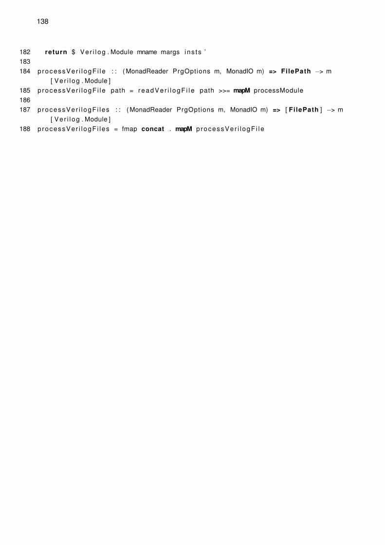
138
182 return $ Ver i l og . Module mname margs ins t s ’183184 p rocessVe r i l ogF i l e : : ( MonadReader PrgOptions m, MonadIO m) => FilePath −> m
[ Ve r i l og . Module ]185 p rocessVe r i l ogF i l e path = r e a d V e r i l o g F i l e path >>= mapM processModule186187 p rocessVer i l ogF i l es : : ( MonadReader PrgOptions m, MonadIO m) => [ FilePath ] −> m
[ Ve r i l og . Module ]188 p rocessVer i l ogF i l es = fmap concat . mapM p rocessVer i l ogF i l e
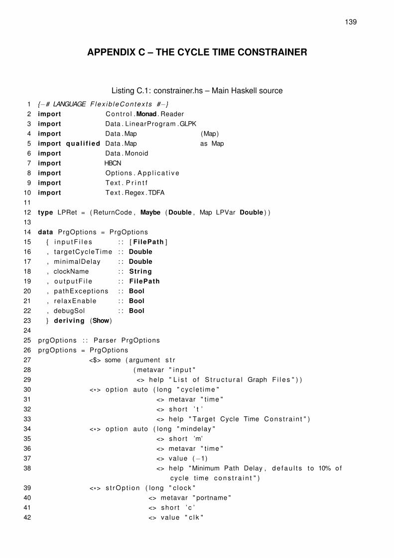
139
APPENDIX C – THE CYCLE TIME CONSTRAINER
Listing C.1: constrainer.hs – Main Haskell source
1 {−# LANGUAGE Flex ib leCon tex ts #−}2 import Cont ro l .Monad . Reader3 import Data . LinearProgram .GLPK4 import Data .Map (Map)5 import qua l i f ied Data .Map as Map6 import Data . Monoid7 import HBCN8 import Options . A p p l i c a t i v e9 import Text . P r i n t f
10 import Text . Regex .TDFA1112 type LPRet = ( ReturnCode , Maybe ( Double , Map LPVar Double ) )1314 data PrgOptions = PrgOptions15 { i n p u t F i l e s : : [ FilePath ]16 , targetCycleTime : : Double17 , minimalDelay : : Double18 , clockName : : String19 , o u t p u t F i l e : : FilePath20 , pathExcept ions : : Bool21 , re laxEnable : : Bool22 , debugSol : : Bool23 } deriving (Show)2425 prgOpt ions : : Parser PrgOptions26 prgOpt ions = PrgOptions27 <$> some ( argument s t r28 ( metavar " i npu t "29 <> help " L i s t o f S t r u c t u r a l Graph F i l e s " ) )30 <*> op t ion auto ( long " cyc le t ime "31 <> metavar " t ime "32 <> shor t ’ t ’33 <> help " Target Cycle Time Cons t ra in t " )34 <*> op t ion auto ( long " mindelay "35 <> shor t ’m’36 <> metavar " t ime "37 <> value (−1)38 <> help " Minimum Path Delay , d e f a u l t s to 10% of
cyc le t ime c o n s t r a i n t " )39 <*> s t rOp t i on ( long " c lock "40 <> metavar " portname "41 <> shor t ’ c ’42 <> value " c l k "
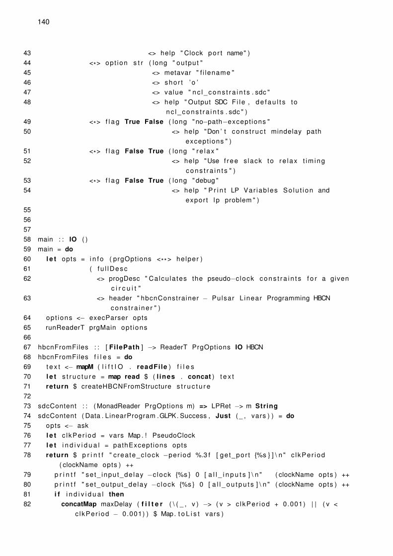
140
43 <> help " Clock po r t name" )44 <*> op t ion s t r ( long " output "45 <> metavar " f i lename "46 <> shor t ’ o ’47 <> value " n c l _ c o n s t r a i n t s . sdc "48 <> help " Output SDC F i le , d e f a u l t s to
n c l _ c o n s t r a i n t s . sdc " )49 <*> f l a g True False ( long " no−path−except ions "50 <> help "Don ’ t cons t ruc t mindelay path
except ions " )51 <*> f l a g False True ( long " re l ax "52 <> help "Use f ree s lack to re l ax t im ing
c o n s t r a i n t s " )53 <*> f l a g False True ( long " debug "54 <> help " P r i n t LP Var iab les So lu t i on and
expor t l p problem " )55565758 main : : IO ( )59 main = do60 l e t opts = i n f o ( prgOpt ions <**> he lper )61 ( f u l lDesc62 <> progDesc " Ca lcu la tes the pseudo−c lock c o n s t r a i n t s f o r a given
c i r c u i t "63 <> header " hbcnConstra iner − Pulsar L inear Programming HBCN
cons t ra i ne r " )64 opt ions <− execParser opts65 runReaderT prgMain opt ions6667 hbcnFromFiles : : [ FilePath ] −> ReaderT PrgOptions IO HBCN68 hbcnFromFiles f i l e s = do69 t e x t <− mapM ( l i f t I O . readFi le ) f i l e s70 l e t s t r u c t u r e = map read $ ( l ines . concat ) t e x t71 return $ createHBCNFromStructure s t r u c t u r e7273 sdcContent : : ( MonadReader PrgOptions m) => LPRet −> m String74 sdcContent ( Data . LinearProgram .GLPK. Success , Just ( _ , vars ) ) = do75 opts <− ask76 l e t c lkPer iod = vars Map . ! PseudoClock77 l e t i n d i v i d u a l = pathExcept ions opts78 return $ p r i n t f " c rea te_c lock −per iod %.3 f [ ge t_por t {%s } ] \ n " c l kPer iod
( clockName opts ) ++79 p r i n t f " se t_ inpu t_de lay −c lock {%s } 0 [ a l l _ i n p u t s ] \ n " ( clockName opts ) ++80 p r i n t f " se t_output_de lay −c lock {%s } 0 [ a l l _ o u t p u t s ] \ n " ( clockName opts ) ++81 i f i n d i v i d u a l then82 concatMap maxDelay ( f i l t e r ( \ ( _ , v ) −> ( v > c lkPer iod + 0.001) | | ( v <
c lkPer iod − 0.001) ) $ Map. t o L i s t vars )

141
83 else [ ]84 where85 maxDelay ( FwDelay src dst , va l )86 | ( s rc =~ " po r t : " ) && ( dst =~ " po r t : " ) =87 p r i n t f " # Forward Delay from %s to %s \ n " src ds t ++88 p r i n t f " set_max_delay −from {%s } −to {%s } %.3 f \ n " ( t r u e R a i l s rc )
( t r u e R a i l ds t ) va l ++89 p r i n t f " set_max_delay −from {%s } −to {%s } %.3 f \ n " ( f a l s e R a i l s rc )
( f a l s e R a i l ds t ) va l ++90 p r i n t f " set_max_delay −from {%s } −to {%s } %.3 f \ n " ( t r u e R a i l s rc )
( f a l s e R a i l ds t ) va l ++91 p r i n t f " set_max_delay −from {%s } −to {%s } %.3 f \ n " ( f a l s e R a i l s rc )
( t r u e R a i l ds t ) va l92 | s rc =~ " po r t : " =93 p r i n t f " # Forward Delay from %s to %s \ n " src ds t ++94 p r i n t f " set_max_delay −from {%s } −to [ get_p in −o f_ob jec ts {%s } − f i l t e r
{ ( i s_c lock_p in == f a l s e ) && ( d i r e c t i o n == i n ) } ] %.3 f \ n " ( t r u e R a i l s rc )( t r u e R a i l ds t ) va l ++
95 p r i n t f " set_max_delay −from {%s } −to [ get_p in −o f_ob jec ts {%s } − f i l t e r{ ( i s_c lock_p in == f a l s e ) && ( d i r e c t i o n == i n ) } ] %.3 f \ n " ( f a l s e R a i l s rc )( f a l s e R a i l ds t ) va l ++
96 p r i n t f " set_max_delay −from {%s } −to [ get_p in −o f_ob jec ts {%s } − f i l t e r{ ( i s_c lock_p in == f a l s e ) && ( d i r e c t i o n == i n ) } ] %.3 f \ n " ( t r u e R a i l s rc )( f a l s e R a i l ds t ) va l ++
97 p r i n t f " set_max_delay −from {%s } −to [ get_p in −o f_ob jec ts {%s } − f i l t e r{ ( i s_c lock_p in == f a l s e ) && ( d i r e c t i o n == i n ) } ] %.3 f \ n " ( f a l s e R a i l s rc )( t r u e R a i l ds t ) va l
98 | otherwise =99 p r i n t f " # Forward Delay from %s to %s \ n " src ds t ++
100 p r i n t f " set_max_delay −from [ get_p in −o f_ob jec ts {%s } − f i l t e r{ i s_c lock_p in == t rue } ] −to [ get_p in −o f_ob jec ts {%s } − f i l t e r{ ( i s_c lock_p in == f a l s e ) && ( d i r e c t i o n == i n ) } ] %.3 f \ n " ( t r u e R a i l s rc )( t r u e R a i l ds t ) va l ++
101 p r i n t f " set_max_delay −from [ get_p in −o f_ob jec ts {%s } − f i l t e r{ i s_c lock_p in == t rue } ] −to [ get_p in −o f_ob jec ts {%s } − f i l t e r{ ( i s_c lock_p in == f a l s e ) && ( d i r e c t i o n == i n ) } ] %.3 f \ n " ( f a l s e R a i l s rc )( f a l s e R a i l ds t ) va l ++
102 p r i n t f " set_max_delay −from [ get_p in −o f_ob jec ts {%s } − f i l t e r{ i s_c lock_p in == t rue } ] −to [ get_p in −o f_ob jec ts {%s } − f i l t e r{ ( i s_c lock_p in == f a l s e ) && ( d i r e c t i o n == i n ) } ] %.3 f \ n " ( t r u e R a i l s rc )( f a l s e R a i l ds t ) va l ++
103 p r i n t f " set_max_delay −from [ get_p in −o f_ob jec ts {%s } − f i l t e r{ i s_c lock_p in == t rue } ] −to [ get_p in −o f_ob jec ts {%s } − f i l t e r{ ( i s_c lock_p in == f a l s e ) && ( d i r e c t i o n == i n ) } ] %.3 f \ n " ( f a l s e R a i l s rc )( t r u e R a i l ds t ) va l
104 maxDelay ( BwDelay src dst , va l )105 | ( s rc =~ " po r t : " ) && ( dst =~ " po r t : " ) =106 p r i n t f " # Backward Delay from %s to %s \ n " src ds t ++
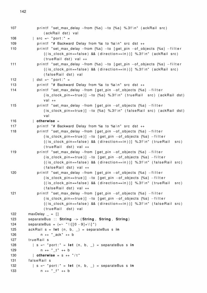
142
107 p r i n t f " set_max_delay −from {%s } −to {%s } %.3 f \ n " ( ackRai l s rc )( ackRai l ds t ) va l
108 | src =~ " po r t : " =109 p r i n t f " # Backward Delay from %s to %s \ n " src ds t ++110 p r i n t f " set_max_delay −from {%s } −to [ get_p in −o f_ob jec ts {%s } − f i l t e r
{ ( i s_c lock_p in == f a l s e ) && ( d i r e c t i o n == i n ) } ] %.3 f \ n " ( ackRai l s rc )( t r u e R a i l ds t ) va l ++
111 p r i n t f " set_max_delay −from {%s } −to [ get_p in −o f_ob jec ts {%s } − f i l t e r{ ( i s_c lock_p in == f a l s e ) && ( d i r e c t i o n == i n ) } ] %.3 f \ n " ( ackRai l s rc )( f a l s e R a i l ds t ) va l
112 | ds t =~ " po r t : " =113 p r i n t f " # Backward Delay from %s to %s \ n " src ds t ++114 p r i n t f " set_max_delay −from [ get_p in −o f_ob jec ts {%s } − f i l t e r
{ i s_c lock_p in == t rue } ] −to {%s } %.3 f \ n " ( t r u e R a i l s rc ) ( ackRai l ds t )va l ++
115 p r i n t f " set_max_delay −from [ get_p in −o f_ob jec ts {%s } − f i l t e r{ i s_c lock_p in == t rue } ] −to {%s } %.3 f \ n " ( f a l s e R a i l s rc ) ( ackRai l ds t )va l
116 | otherwise =117 p r i n t f " # Backward Delay from %s to %s \ n " src ds t ++118 p r i n t f " set_max_delay −from [ get_p in −o f_ob jec ts {%s } − f i l t e r
{ i s_c lock_p in == t rue } ] −to [ get_p in −o f_ob jec ts {%s } − f i l t e r{ ( i s_c lock_p in == f a l s e ) && ( d i r e c t i o n == i n ) } ] %.3 f \ n " ( t r u e R a i l s rc )( t r u e R a i l ds t ) va l ++
119 p r i n t f " set_max_delay −from [ get_p in −o f_ob jec ts {%s } − f i l t e r{ i s_c lock_p in == t rue } ] −to [ get_p in −o f_ob jec ts {%s } − f i l t e r{ ( i s_c lock_p in == f a l s e ) && ( d i r e c t i o n == i n ) } ] %.3 f \ n " ( f a l s e R a i l s rc )( f a l s e R a i l ds t ) va l ++
120 p r i n t f " set_max_delay −from [ get_p in −o f_ob jec ts {%s } − f i l t e r{ i s_c lock_p in == t rue } ] −to [ get_p in −o f_ob jec ts {%s } − f i l t e r{ ( i s_c lock_p in == f a l s e ) && ( d i r e c t i o n == i n ) } ] %.3 f \ n " ( t r u e R a i l s rc )( f a l s e R a i l ds t ) va l ++
121 p r i n t f " set_max_delay −from [ get_p in −o f_ob jec ts {%s } − f i l t e r{ i s_c lock_p in == t rue } ] −to [ get_p in −o f_ob jec ts {%s } − f i l t e r{ ( i s_c lock_p in == f a l s e ) && ( d i r e c t i o n == i n ) } ] %.3 f \ n " ( f a l s e R a i l s rc )( t r u e R a i l ds t ) va l
122 maxDelay _ = [ ]123 separateBus : : String −> ( String , String , String )124 separateBus = (=~ " \ \ [ [ 0 − 9 ] + \ \ ] " )125 ackRai l s = l e t ( n , b , _ ) = separateBus s in126 n ++ " _ack " ++ b127 t r u e R a i l s128 | s =~ " po r t : " = l e t ( n , b , _ ) = separateBus s in129 n ++ " _ t " ++ b130 | otherwise = s ++ " / t "131 f a l s e R a i l s132 | s =~ " po r t : " = l e t ( n , b , _ ) = separateBus s in133 n ++ " _ f " ++ b
143
134 | otherwise = s ++ " / f "135136 sdcContent e r r = er rorWi thoutStackTrace . p r i n t f " Could not so lve LP : %s " $
show e r r137138 p r i n t S o l u t i o n : : ( MonadIO m) => LPRet −> m ( )139 p r i n t S o l u t i o n ( Data . LinearProgram .GLPK. Success , Just ( _ , vars ) ) = l i f t I O $140 mapM_ pr in t $ Map. t o L i s t vars141 p r i n t S o l u t i o n e r r = er rorWi thoutStackTrace . p r i n t f " Could not so lve LP : %s " $
show e r r142143 lpOb jec t i ve : : LPRet −> Double144 lpOb jec t i ve ( Data . LinearProgram .GLPK. Success , Just ( o , _ ) ) = o145 lpOb jec t i ve e r r = er rorWi thoutStackTrace . p r i n t f " Could not so lve LP : %s " $
show e r r146147 prgMain : : ReaderT PrgOptions IO ( )148 prgMain = do149 opts <− ask150 hbcn <− hbcnFromFiles $ i n p u t F i l e s opts151 l e t cycleTime = targetCycleTime opts152 l e t r e l ax = re laxEnable opts153 l e t minDelay = case minimalDelay opts of154 x | x < 0 −> cycleTime /10155 | otherwise −> x156 l e t l p = const ra in tCyc leT ime hbcn cycleTime minDelay re l ax157 r e s u l t <− l i f t I O $ glpSolveVars s imp lexDefau l ts l p158 sdc <− sdcContent r e s u l t159 when ( debugSol opts ) $ do160 l e t l p f i l e = o u t p u t F i l e opts ++ " . l p "161 p r i n t S o l u t i o n r e s u l t162 l i f t I O $ wr i teLP l p f i l e l p163 l i f t I O $ i f l pOb jec t i ve r e s u l t > 0.0005 then do164 p r i n t f " Wr i t i ng c o n s t r a i n t s to %s \ n " ( o u t p u t F i l e opts )165 wr i teF i le ( o u t p u t F i l e opts ) sdc166 else167 errorWi thoutStackTrace " Deadlock Found i n the Design , not w r i t i n g
c o n s t r a i n t s f i l e "
Listing C.2: src/Data/HBCN.hs
1 module HBCN2 ( module HBCN. Timing3 , module HBCN. I n t e r n a l4 ) where56 import HBCN. I n t e r n a l7 import HBCN. Timing

144
Listing C.3: src/Data/HBCN/Internal.hs – Structural graph to HBCN
1 module HBCN. I n t e r n a l where23 import Algebra . Graph . Label led4 import Data . Semigroup as SG56 data St ruc tu ra lE lement = Por t String [ String ]7 | DataReg String [ String ]8 | NullReg String [ String ]9 deriving (Show, Read , Eq , Ord )
1011 data T r a n s i t i o n = DataTrans {nodeName : : String }12 | Nul lTrans {nodeName : : String }13 deriving (Show, Read , Eq , Ord )1415 data Place = Unconnected16 | Place { hasToken : : Bool }17 | MindelayPlace { hasToken : : Bool }18 deriving (Show, Read , Eq , Ord )1920 type HBCN = Graph Place T r a n s i t i o n2122 instance Semigroup Place where23 Unconnected <> a = a24 a <> _ = a2526 instance Monoid Place where27 mempty = Unconnected28 mappend = (SG. < >)2930 createHBCNFromStructure : : [ S t ruc tu ra lE lement ] −> HBCN31 createHBCNFromStructure = edges . concatMap go where32 go ( Por t s rc ds t ) = concatMap33 ( \ x −> [ ( Place False , DataTrans src , DataTrans x )34 , ( Place False , Nu l lTrans src , Nul lTrans x )35 , ( Place False , DataTrans x , Nul lTrans src )36 , ( Place True , Nu l lTrans x , DataTrans src ) ] ) ds t37 go ( NullReg src dst ) = concatMap38 ( \ x −> [ ( Place False , DataTrans src , DataTrans x )39 , ( Place False , Nu l lTrans src , Nul lTrans x )40 , ( Place False , DataTrans x , Nul lTrans src )41 , ( Place True , Nu l lTrans x , DataTrans src ) ] ) ds t42 go ( DataReg src dst ) =43 l e t44 sout = src ++ " / sout "45 sin = src ++ " / s in "46 in −− I npu t Slave

145
47 [ ( MindelayPlace False , DataTrans src , DataTrans sin )48 , ( MindelayPlace True , Nu l lTrans src , Nul lTrans sin )49 , ( MindelayPlace False , DataTrans sin , Nu l lTrans src )50 , ( MindelayPlace False , Nu l lTrans sin , DataTrans src )51 −− Data stage52 , ( MindelayPlace True , DataTrans sin , DataTrans sout )53 , ( MindelayPlace False , Nu l lTrans sin , Nu l lTrans sout )54 , ( MindelayPlace False , DataTrans sout , Nul lTrans sin )55 , ( MindelayPlace False , Nu l lTrans sout , DataTrans sin ) ] ++56 −− Output s lave57 concatMap ( \ x −> [ ( Place False , DataTrans sout , DataTrans x )58 , ( Place False , Nu l lTrans sout , Nul lTrans x )59 , ( Place False , DataTrans x , Nul lTrans sout )60 , ( Place True , Nu l lTrans x , DataTrans sout ) ] ) ds t
Listing C.4: src/Data/HBCN/Timing.hs – HBCN cycle time constrainer
1 {−# LANGUAGE Flex ib leCon tex ts #−}2 module HBCN. Timing3 ( LPVar ( . . )4 , TimingLP5 , const ra in tCyc leT ime ) where67 import Algebra . Graph . Label led8 import Cont ro l .Monad9 import Data . LinearProgram
10 import HBCN. I n t e r n a l11 import Prelude hiding (Num ( . . ) )1213 data LPVar = A r r i v a l T r a n s i t i o n14 | FwDelay String String15 | BwDelay String String16 | FwSlack String String17 | BwSlack String String18 | PseudoClock19 deriving (Show, Read , Eq , Ord )2021 type TimingLP = LP LPVar Double2223 ar r iva lT imeEq cycleTime minDelay re l ax ( place , src , ds t ) = do24 l e t src ’ = A r r i v a l s rc25 l e t dst ’ = A r r i v a l ds t26 l e t c t = i f hasToken place then cycleTime else 027 l e t s lack = case ( src , ds t ) of28 ( DataTrans s , DataTrans d ) −> FwSlack s d29 ( Nul lTrans s , Nul lTrans d ) −> FwSlack s d30 ( DataTrans s , Nul lTrans d ) −> BwSlack s d31 ( Nul lTrans s , DataTrans d ) −> BwSlack s d

146
32 l e t delay = case ( src , ds t ) of33 ( DataTrans s , DataTrans d ) −> FwDelay s d34 ( Nul lTrans s , Nul lTrans d ) −> FwDelay s d35 ( DataTrans s , Nul lTrans d ) −> BwDelay s d36 ( Nul lTrans s , DataTrans d ) −> BwDelay s d37 setVarBounds delay $ LBound minDelay38 setVarBounds s lack $ LBound 039 setVarBounds src ’ $ LBound 040 setVarBounds dst ’ $ LBound 041 i f r e l ax42 then do43 l inCombinat ion [ ( 1 , src ’ ) , (−1 , dst ’ ) , (1 , delay ) ] ‘ equalTo ‘ c t44 case place of45 MindelayPlace _ −> l inCombinat ion [ ( 1 , delay ) , (−1 , s lack ) ] ‘ equalTo ‘
minDelay46 _ −> l inCombinat ion [ ( 1 , delay ) ] ‘ equal ‘ l inCombinat ion [ ( 1 ,
PseudoClock ) , (1 , s lack ) ]47 else do48 l inCombinat ion [ ( 1 , src ’ ) , (−1 , dst ’ ) , (1 , delay ) , (1 , s lack ) ] ‘ equalTo ‘ c t49 case place of50 MindelayPlace _ −> l inCombinat ion [ ( 1 , delay ) ] ‘ equalTo ‘ minDelay51 _ −> l inCombinat ion [ ( 1 , delay ) ] ‘ equal ‘ l inCombinat ion [ ( 1 , PseudoClock ) ]5253 const ra in tCyc leT ime : : HBCN −> Double −> Double −> Bool −> TimingLP54 const ra in tCyc leT ime hbcn cycleTime minDelay re l ax = execLPM $ do55 s e t D i r e c t i o n Max56 se tOb jec t i ve $ l inCombinat ion [ ( 1 , PseudoClock ) ]57 setVarBounds PseudoClock $ LBound minDelay58 mapM_ ( a r r iva lT imeEq cycleTime minDelay re l ax ) $ edgeLis t hbcn
147
APPENDIX D – THE PSEUDO-SYNCHRONOUS SYNTHESIS SCRIPTS
Listing D.1: circuits/design/syn_st65.tcl
1 source . . / . . / s c r i p t s / f i x n e t l i s t . t c l23 set PERIOD $: :env (PERIOD)45 set DESIGN $: :env (DESIGN)6 set OUTDIR output / $ {PERIOD}78 f i l e mkdir $ {OUTDIR}9
10 s h e l l hbcnConstra iner $ {DESIGN} .graph −m 0 .2 −t $ {PERIOD} −o$ {OUTDIR } / n c l _ c o n s t r a i n t s . s d c
1112 set_db auto_super_thread t rue13 set_db s y n _ g l o b a l _ e f f o r t h igh14 #set_db leakage_power_ef for t medium15 set_db syn_op t_e f f o r t extreme16 set_db tns_opto t rue17 set_db a u t o _ p a r t i t i o n t rue18 set_db avo id_ t i ed_ inpu ts t rue1920 read_mmmc st65_mmmc.tcl21 set_db l e f _ l i b r a r y {22 . . / . . / tech / CORE65GPSVT_soc.lef23 . . / . . / tech / PRHS65_soc.lef24 . . / . . / tech / cmos065_7m4x0y2z_AP_Worst.lef25 . . / . . / tech / ASCEND_NCLP65GPSVT.lef26 . . / . . / tech / ASCEND_NCL65GPSVT.lef27 }2829 source . . / . . / tech / s t 6 5 . t c l3031 read_hdl −sv . . / . . / tech / drexpansion.sv32 read_hdl −sv ncl_$ {DESIGN} . v33 e labora te $ {DESIGN}3435 i n i t _ d e s i g n3637 set i n s t s [ a l l : : a l l _ s e q s ]38 i f { [ l length $ i n s t s ] > 0} {39 se t_s ize_on ly $ i n s t s t rue40 }4142 set_db i o p t _ u l t r a _ o p t i m i z a t i o n t rue

148
43 set_dont_use [ n c l p _ c e l l _ l i s t ] t r ue44 syn_gener ic45 syn_map4647 syn_opt48 syn_opt −physical49 syn_opt − incremental −physical5051 f i x _ x n e t l i s t5253 opt_sdds 105455 prepare_ fo r_phys ica l5657 set_db write_vlog_wor_wand f a l s e58 r e p o r t _ t i m i n g −nworst 1000 > $ {OUTDIR } / t i m i n g . r p t59 repor t_ga tes > $ {OUTDIR } / g a t e s . r p t60 report_power > $ {OUTDIR } / power . rp t61 w r i t e_ h d l > $ {OUTDIR } / l o g i c a l . v62 wr i te_snapshot −innovus −outd i r $ {OUTDIR } / snapshot −tag l o g i c a l6364 set_ana lys is_v iew −setup wors t_ la tch_v iew65 w r i t e_ s d f > $ {OUTDIR } / w o r s t . sd f6667 set_ana lys is_v iew −setup nominal_ latch_view68 w r i t e_ s d f > $ {OUTDIR } / nomina l .sd f6970 set_ana lys is_v iew −setup best_ la tch_v iew71 w r i t e_ s d f > $ {OUTDIR } / b e s t . s d f
Listing D.2: scripts/fixnetlist.tcl
1 proc get_adjacent_nodes { node } {2 var iable r e t3 set r e t [ l i s t ]45 foreach { a } [ get_db − i f { . ob j_ t ype == pin } \6 [ get_ fanout −max_pin_depth 1 $node ] ] {7 i f [ get_db [ vdirname $a ] . i s_comb ina t i ona l ] {8 lappend r e t $a9 }
10 }1112 return $ re t13 }1415 proc get_ ins tance_of_p in { p in } {16 return [ vdirname $pin ]
149
17 }1819 proc get_ ins t_ce l l_name { i n s t } {20 return [ vbasename [ get_db $ i n s t . l i b _ c e l l ] ]21 }2223 proc rep lace_ ins t_ga te { i n s t gate } {24 change_l ink − instances $ i n s t − l i b _ c e l l [ l index [ v f i n d / − l i b _ c e l l $gate ] 0 ]25 }2627 proc ge t_ba r r i e r s_ou tpu t { } {28 return [ a l l : : a l l _ s e q s −output_pins ]29 }3031 proc i s_nc lp { ins tance } {32 global n c l p _ c e l l33 return [ info exists n c l p _ c e l l ( [ get_ ins t_ce l l_name $ { ins tance } ] ) ]34 }3536 proc i s _ n c l { ins tance } {37 global n c l _ c e l l38 return [ info exists n c l _ c e l l ( [ get_ ins t_ce l l_name $ { ins tance } ] ) ]39 }4041 proc n c l _ c e l l _ l i s t { } {42 global n c l _ c e l l43 return [ array names n c l _ c e l l ]44 }4546 proc n c l p _ c e l l _ l i s t { } {47 global n c l p _ c e l l48 return [ array names n c l p _ c e l l ]49 }5051 proc o r p h a n _ c e l l _ l i s t { } {52 global orphan_ce l l53 return [ array names orphan_ce l l ]54 }5556 proc get_domain_pins { r t z p i n s v a r r t o p i n s v a r } {57 global r t z _ s t a r t p o i n t s58 global r t o _ s t a r t p o i n t s59 upvar 1 $ r t z p i n s v a r r t z p i n s l i s t60 upvar 1 $ r top insva r r t o p i n s l i s t6162 var iable r t z p i n s63 var iable r t o p i n s64 var iable v i s i t e d

150
6566 i f { ! [ info exists r t z _ s t a r t p o i n t s ] | | ! [ info exists r t o _ s t a r t p o i n t s ] } {67 set r t z _ s t a r t p o i n t s [ concat [ v f i n d / −port * ] [ a l l : : a l l _ s e q s −output_pins ] ]68 }6970 i f [ info exists r t z _ s t a r t p o i n t s ] {71 foreach { p in } $ r t z _ s t a r t p o i n t s {72 foreach { a } [ get_adjacent_nodes $pin ] {73 incr r t z p i n s ( $a )74 }75 }76 }7778 i f [ info exists r t o _ s t a r t p o i n t s ] {79 foreach { p in } $ r t o _ s t a r t p o i n t s {80 foreach { a } [ get_adjacent_nodes $pin ] {81 incr r t o p i n s ( $a )82 }83 }84 }8586 var iable done87 set done 088 while { ! $done } {89 set done 190 #breath f i r s t RTZ pins processing91 foreach { a } [ array names r t z p i n s ] {92 i f { ! [ info exists v i s i t e d ( $a ) ] | | ! $ v i s i t e d ( $a ) } {93 i f [ i s _ i n v e r t i n g _ o u t p u t $a ] {94 # i n v e r s i o n found95 foreach { b } [ get_adjacent_nodes $a ] {96 incr r t o p i n s ( $b )97 }98 } else {99 #no domain i n v e r s i o n
100 foreach { b } [ get_adjacent_nodes $a ] {101 incr r t z p i n s ( $b )102 }103 }104 incr v i s i t e d ( $a )105 set done 0106 }107 }108109 # breath f i r s t RTO pins processing110 foreach { a } [ array names r t o p i n s ] {111 i f { ! [ info exists v i s i t e d ( $a ) ] | | ! $ v i s i t e d ( $a ) } {112 i f [ i s _ i n v e r t i n g _ o u t p u t $a ] {

151
113 # i n v e r s i o n found114 foreach { b } [ get_adjacent_nodes $a ] {115 incr r t z p i n s ( $b )116 }117 } else {118 #no domain i n v e r s i o n119 foreach { b } [ get_adjacent_nodes $a ] {120 incr r t o p i n s ( $b )121 }122 }123 incr v i s i t e d ( $a )124 set done 0125 }126 }127 }128129 unset −nocomplain r t o p i n s l i s t130 unset −nocomplain r t o p i n s l i s t131132 set r t o p i n s l i s t [ l so r t −unique [ array names r t o p i n s ] ]133 set r t z p i n s l i s t [ l so r t −unique [ array names r t z p i n s ] ]134135 unset −nocomplain r t z p i n s136 unset −nocomplain r t o p i n s137 unset −nocomplain v i s i t e d138139 return 1140 }141142 proc get_domain_instances { r t z i n s t s v a r r t o i n s t s v a r } {143 upvar 1 $ r t z i n s t s v a r r t z i n s t s144 upvar 1 $ r t o i n s t s v a r r t o i n s t s145146 var iable r t op147 var iable r t z p148149 get_domain_pins r t z p r top150151 # get i ns tance names from pin names152 set r t z i n s t s [ l i s t ]153 foreach { a } $ { r t z p } {154 lappend r t z i n s t s [ ge t_ ins tance_of_p in $a ]155 }156 set r t z i n s t s [ l so r t −unique $ r t z i n s t s ]157158 set r t o i n s t s [ l i s t ]159 foreach { a } $ { r t op } {160 lappend r t o i n s t s [ ge t_ ins tance_of_p in $a ]
152
161 }162 set r t o i n s t s [ l so r t −unique $ r t o i n s t s ]163164 unset −nocomplain r t z p i n s165 unset −nocomplain r t o p i n s166167 return 1168 }169170 proc f i x _ x n e t l i s t { } {171 var iable r t z172 var iable r t o173 var iable count174 global e q u i v a l e n t _ c e l l175176 set count 0177178 get_domain_instances r t z r t o179180 foreach { i } $ r t o {181 i f { [ lsearch −sorted $ r t z $ i ] >= 0} {182 return −code error " $ { i } i s i n both RTO and RTZ domains "183 }184 }185186 foreach { i } $ r t z {187 i f { [ i s_nc lp $ i ] } {188 var iable l n189 var iable n ln190 set l n [ get_ ins t_ce l l_name $ i ]191 set n ln $ e q u i v a l e n t _ c e l l ( $ ln )192 puts " Replacing $ { i } from $ { l n } to $ { n ln } "193 rep lace_ ins t_ga te $ i $nln194 incr count195 }196 }197198 foreach { i } $ r t o {199 i f { [ i s _ n c l $ i ] } {200 var iable l n201 var iable n ln202 set l n [ get_ ins t_ce l l_name $ i ]203 set n ln $ e q u i v a l e n t _ c e l l ( $ ln )204 puts " Replacing $ { i } from $ { l n } to $ { n ln } "205 rep lace_ ins t_ga te $ i $nln206 incr count207 }208 }

153
209210 return $count211 }212213 proc check_sdds_consistency { } {214 var iable r t z215 var iable r t o216 var iable r e t217218 get_domain_instances r t z r t o219220 set r e t 1221222 foreach { i } $ r t o {223 i f { [ lsearch −sorted $ r t z $ i ] >= 0} {224 puts " $ { i } i s i n both RTO and RTZ domains "225 set r e t 0226 }227 }228229 foreach { i } $ r t z {230 i f { [ i s_nc lp $ i ] } {231 puts " $ { i } i s a NCLP c e l l i n the RTZ domain "232 set r e t 0233 }234 }235236 foreach { i } $ r t o {237 i f { [ i s _ n c l $ i ] } {238 puts " $ { i } i s a NCL c e l l i n the RTO domain "239 set r e t 0240 }241 }242243 return $ re t244 }245246 proc o p t _ r t z { } {247248 puts " Opt imis ing RTZ Gates "249250 set_dont_use [ n c l _ c e l l _ l i s t ] f a l s e251 set_dont_touch [ n c l _ c e l l _ l i s t ] f a l s e252 set_dont_use [ n c l p _ c e l l _ l i s t ] t r ue253 set_dont_touch [ n c l p _ c e l l _ l i s t ] t r ue254 syn_opt − incremental −physical255256 set_dont_use [ n c l p _ c e l l _ l i s t ] f a l s e

154
257 set_dont_touch [ n c l p _ c e l l _ l i s t ] f a l s e258259 return [ f i x _ x n e t l i s t ]260 }261262 proc op t_ r t o { } {263264 puts " Opt imis ing RTO Gates "265266 set_dont_use [ n c l _ c e l l _ l i s t ] t r ue267 set_dont_touch [ n c l _ c e l l _ l i s t ] t r ue268 set_dont_use [ n c l p _ c e l l _ l i s t ] f a l s e269 set_dont_touch [ n c l p _ c e l l _ l i s t ] f a l s e270 syn_opt − incremental −physical271272 set_dont_use [ n c l _ c e l l _ l i s t ] f a l s e273 set_dont_touch [ n c l _ c e l l _ l i s t ] f a l s e274275 return [ f i x _ x n e t l i s t ]276 }277278 proc opt_sdds { maxi t } {279 var iable i t280281 set i t 0282 phys_opt_r to283 phys_opt_r tz284285 while { $ i t < $maxit } {286 puts "SDDS Opt im isa t ion i t e r a t i o n $ { i t } "287 incr i t288289 i f [ op t_ r t o ] {290 phys_opt_r tz291 }292293 i f [ o p t _ r t z ] {294 phys_opt_r to295 }296297 i f { [ get_db [ cur ren t_des ign ] . s l a c k ] >= 0} {298 break299 }300 }301302 return $ i t303 }304
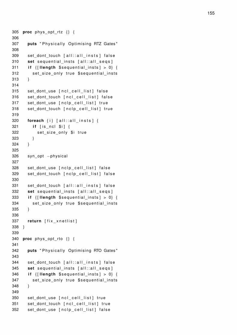
155
305 proc phys_opt_r tz { } {306307 puts " P h y s i c a l l y Opt imis ing RTZ Gates "308309 set_dont_touch [ a l l : : a l l _ i n s t s ] f a l s e310 set s e q u e n t i a l _ i n s t s [ a l l : : a l l _ s e q s ]311 i f { [ l length $sequen t i a l _ i ns t s ] > 0} {312 se t_s ize_on ly t rue $sequen t i a l _ i ns t s313 }314315 set_dont_use [ n c l _ c e l l _ l i s t ] f a l s e316 set_dont_touch [ n c l _ c e l l _ l i s t ] f a l s e317 set_dont_use [ n c l p _ c e l l _ l i s t ] t r ue318 set_dont_touch [ n c l p _ c e l l _ l i s t ] t r ue319320 foreach { i } [ a l l : : a l l _ i n s t s ] {321 i f [ i s _ n c l $ i ] {322 se t_s ize_on ly $ i t r ue323 }324 }325326 syn_opt −physical327328 set_dont_use [ n c l p _ c e l l _ l i s t ] f a l s e329 set_dont_touch [ n c l p _ c e l l _ l i s t ] f a l s e330331 set_dont_touch [ a l l : : a l l _ i n s t s ] f a l s e332 set s e q u e n t i a l _ i n s t s [ a l l : : a l l _ s e q s ]333 i f { [ l length $sequen t i a l _ i ns t s ] > 0} {334 se t_s ize_on ly t rue $sequen t i a l _ i ns t s335 }336337 return [ f i x _ x n e t l i s t ]338 }339340 proc phys_opt_r to { } {341342 puts " P h y s i c a l l y Opt imis ing RTO Gates "343344 set_dont_touch [ a l l : : a l l _ i n s t s ] f a l s e345 set s e q u e n t i a l _ i n s t s [ a l l : : a l l _ s e q s ]346 i f { [ l length $sequen t i a l _ i ns t s ] > 0} {347 se t_s ize_on ly t rue $sequen t i a l _ i ns t s348 }349350 set_dont_use [ n c l _ c e l l _ l i s t ] t r ue351 set_dont_touch [ n c l _ c e l l _ l i s t ] t r ue352 set_dont_use [ n c l p _ c e l l _ l i s t ] f a l s e
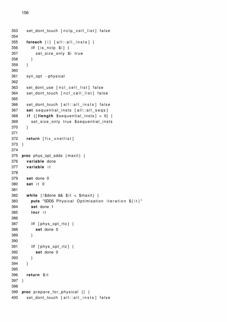
156
353 set_dont_touch [ n c l p _ c e l l _ l i s t ] f a l s e354355 foreach { i } [ a l l : : a l l _ i n s t s ] {356 i f [ i s_nc lp $ i ] {357 se t_s ize_on ly $ i t r ue358 }359 }360361 syn_opt −physical362363 set_dont_use [ n c l _ c e l l _ l i s t ] f a l s e364 set_dont_touch [ n c l _ c e l l _ l i s t ] f a l s e365366 set_dont_touch [ a l l : : a l l _ i n s t s ] f a l s e367 set s e q u e n t i a l _ i n s t s [ a l l : : a l l _ s e q s ]368 i f { [ l length $sequen t i a l _ i ns t s ] > 0} {369 se t_s ize_on ly t rue $sequen t i a l _ i ns t s370 }371372 return [ f i x _ x n e t l i s t ]373 }374375 proc phys_opt_sdds { maxi t } {376 var iable done377 var iable i t378379 set done 0380 set i t 0381382 while { ! $done && $ i t < $maxit } {383 puts "SDDS Phys ica l Op t im isa t ion i t e r a t i o n $ { i t } "384 set done 1385 incr i t386387 i f [ phys_opt_r to ] {388 set done 0389 }390391 i f [ phys_opt_r tz ] {392 set done 0393 }394 }395396 return $ i t397 }398399 proc prepare_ fo r_phys ica l { } {400 set_dont_touch [ a l l : : a l l _ i n s t s ] f a l s e

157
401 set s e q u e n t i a l _ i n s t s [ a l l : : a l l _ s e q s ]402 i f { [ l length $sequen t i a l _ i ns t s ] > 0} {403 se t_s ize_on ly t rue $sequen t i a l _ i ns t s404 }405406 set_dont_touch [ n c l p _ c e l l _ l i s t ] t r ue407 set_dont_use [ n c l p _ c e l l _ l i s t ] t r ue408409 set_dont_touch [ n c l _ c e l l _ l i s t ] f a l s e410 set_dont_use [ n c l _ c e l l _ l i s t ] f a l s e411412 foreach { i } [ a l l : : a l l _ i n s t s ] {413 i f [ i s _ n c l $ i ] {414 se t_s ize_on ly $ i t r ue415 }416 }417418 return 1419 }420421 # fo rces o p t i m i s a t i o n to not use constants422 set_db iop t_ fo rce_constan t_remova l t r ue423424 # Local V a r i a b l e s :425 # mode: t c l426 # t c l− i n d e n t− l e v e l : 2427 # indent−tabs−mode: n i l428 # End:
Listing D.3: circuits/design/st65_mmmc.tcl
1 ## l i b r a r y _ s e t s2 c r e a t e _ l i b r a r y _ s e t −name w o r s t _ f l o p _ l i b s e t \3 − t iming { . . / . . / tech / CORE65GPSVT_wc_0.90V_125C.lib \4 . . / . . / tech / ASCEND_NCL65GPSVT_SS_0.90V_125C_letiflop.lib \5 . . / . . / tech / ASCEND_NCLP65GPSVT_SS_0.90V_125C.lib }67 c r e a t e _ l i b r a r y _ s e t −name n o m i n a l _ f l o p _ l i b s e t \8 − t iming { . . / . . / tech / CORE65GPSVT_nom_1.00V_25C.lib \9 . . / . . / tech / ASCEND_NCL65GPSVT_TT_1.00V_25C_letiflop.lib \
10 . . / . . / tech / ASCEND_NCLP65GPSVT_TT_1.00V_25C.lib }1112 c r e a t e _ l i b r a r y _ s e t −name b e s t _ f l o p _ l i b s e t \13 − t iming { . . / . . / tech / CORE65GPSVT_bc_1.10V_m40C.lib \14 . . / . . / tech / ASCEND_NCL65GPSVT_FF_1.10V_m40C_letiflop.lib \15 . . / . . / tech / ASCEND_NCLP65GPSVT_FF_1.10V_m40C.lib }1617 c r e a t e _ l i b r a r y _ s e t −name w o r s t _ l a t c h _ l i b s e t \
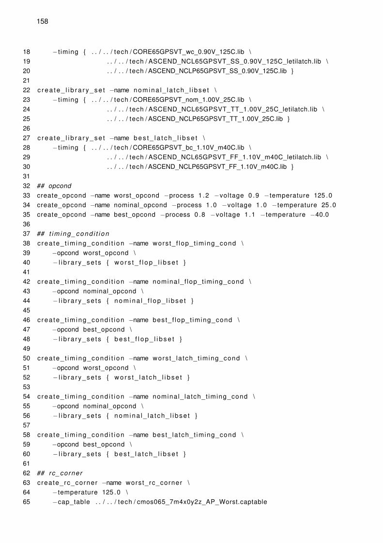
158
18 − t iming { . . / . . / tech / CORE65GPSVT_wc_0.90V_125C.lib \19 . . / . . / tech / ASCEND_NCL65GPSVT_SS_0.90V_125C_letilatch.lib \20 . . / . . / tech / ASCEND_NCLP65GPSVT_SS_0.90V_125C.lib }2122 c r e a t e _ l i b r a r y _ s e t −name n o m i n a l _ l a t c h _ l i b s e t \23 − t iming { . . / . . / tech / CORE65GPSVT_nom_1.00V_25C.lib \24 . . / . . / tech / ASCEND_NCL65GPSVT_TT_1.00V_25C_letilatch.lib \25 . . / . . / tech / ASCEND_NCLP65GPSVT_TT_1.00V_25C.lib }2627 c r e a t e _ l i b r a r y _ s e t −name b e s t _ l a t c h _ l i b s e t \28 − t iming { . . / . . / tech / CORE65GPSVT_bc_1.10V_m40C.lib \29 . . / . . / tech / ASCEND_NCL65GPSVT_FF_1.10V_m40C_letilatch.lib \30 . . / . . / tech / ASCEND_NCLP65GPSVT_FF_1.10V_m40C.lib }3132 ## opcond33 create_opcond −name worst_opcond −process 1 .2 −voltage 0 .9 −temperature 125 .034 create_opcond −name nominal_opcond −process 1 .0 −voltage 1 .0 −temperature 25 .035 create_opcond −name best_opcond −process 0 .8 −voltage 1 .1 −temperature −40.03637 ## t i m i ng _ co n d i t i on38 c rea te_ t im ing_cond i t i on −name wors t_ f lop_t iming_cond \39 −opcond worst_opcond \40 − l i b ra r y_se t s { w o r s t _ f l o p _ l i b s e t }4142 c rea te_ t im ing_cond i t i on −name nominal_f lop_t iming_cond \43 −opcond nominal_opcond \44 − l i b ra r y_se t s { n o m i n a l _ f l o p _ l i b s e t }4546 c rea te_ t im ing_cond i t i on −name best_ f lop_t iming_cond \47 −opcond best_opcond \48 − l i b ra r y_se t s { b e s t _ f l o p _ l i b s e t }4950 c rea te_ t im ing_cond i t i on −name wors t_ la tch_t iming_cond \51 −opcond worst_opcond \52 − l i b ra r y_se t s { w o r s t _ l a t c h _ l i b s e t }5354 c rea te_ t im ing_cond i t i on −name nominal_ la tch_t iming_cond \55 −opcond nominal_opcond \56 − l i b ra r y_se t s { n o m i n a l _ l a t c h _ l i b s e t }5758 c rea te_ t im ing_cond i t i on −name best_ la tch_t iming_cond \59 −opcond best_opcond \60 − l i b ra r y_se t s { b e s t _ l a t c h _ l i b s e t }6162 ## rc_corner63 create_rc_corner −name wors t_rc_corner \64 −temperature 125 .0 \65 −cap_table . . / . . / tech / cmos065_7m4x0y2z_AP_Worst.captable

159
6667 crea te_rc_corner −name nominal_rc_corner \68 −temperature 25 .0 \69 −cap_table . . / . . / tech / cmos065_7m4x0y2z_AP_Worst.captable7071 crea te_rc_corner −name best_rc_corner \72 −temperature −40.0 \73 −cap_table . . / . . / tech / cmos065_7m4x0y2z_AP_Best.captable7475 ## delay_corner76 create_delay_corner −name wors t_ f lop_de lay_corner \77 − t im ing_cond i t ion wors t_ f lop_t iming_cond \78 −rc_corner wors t_rc_corner7980 create_delay_corner −name nomina l_ f lop_delay_corner \81 − t im ing_cond i t ion nominal_ f lop_t iming_cond \82 −rc_corner nominal_rc_corner8384 create_delay_corner −name best_ f lop_de lay_corner \85 − t im ing_cond i t ion best_ f lop_t iming_cond \86 −rc_corner best_rc_corner8788 create_delay_corner −name wors t_ la tch_de lay_corner \89 − t im ing_cond i t ion wors t_ la tch_t iming_cond \90 −rc_corner wors t_rc_corner9192 create_delay_corner −name nomina l_ la tch_delay_corner \93 − t im ing_cond i t ion nominal_ la tch_t iming_cond \94 −rc_corner nominal_rc_corner9596 create_delay_corner −name best_ la tch_de lay_corner \97 − t im ing_cond i t ion best_ la tch_t iming_cond \98 −rc_corner best_rc_corner99
100 ## constraint_mode101 create_constra int_mode −name d e f a u l t _ c o n s t r a i n t s \102 −sdc_f i les { c o n s t r a i n t s . s d c }103104 ## analys is_v iew105 create_ana lys is_v iew −name wors t_ f lop_v iew \106 −constraint_mode d e f a u l t _ c o n s t r a i n t s \107 −delay_corner wors t_ f lop_de lay_corner108109 create_ana lys is_v iew −name nominal_f lop_view \110 −constraint_mode d e f a u l t _ c o n s t r a i n t s \111 −delay_corner nomina l_ f lop_delay_corner112113 create_ana lys is_v iew −name best_ f lop_v iew \
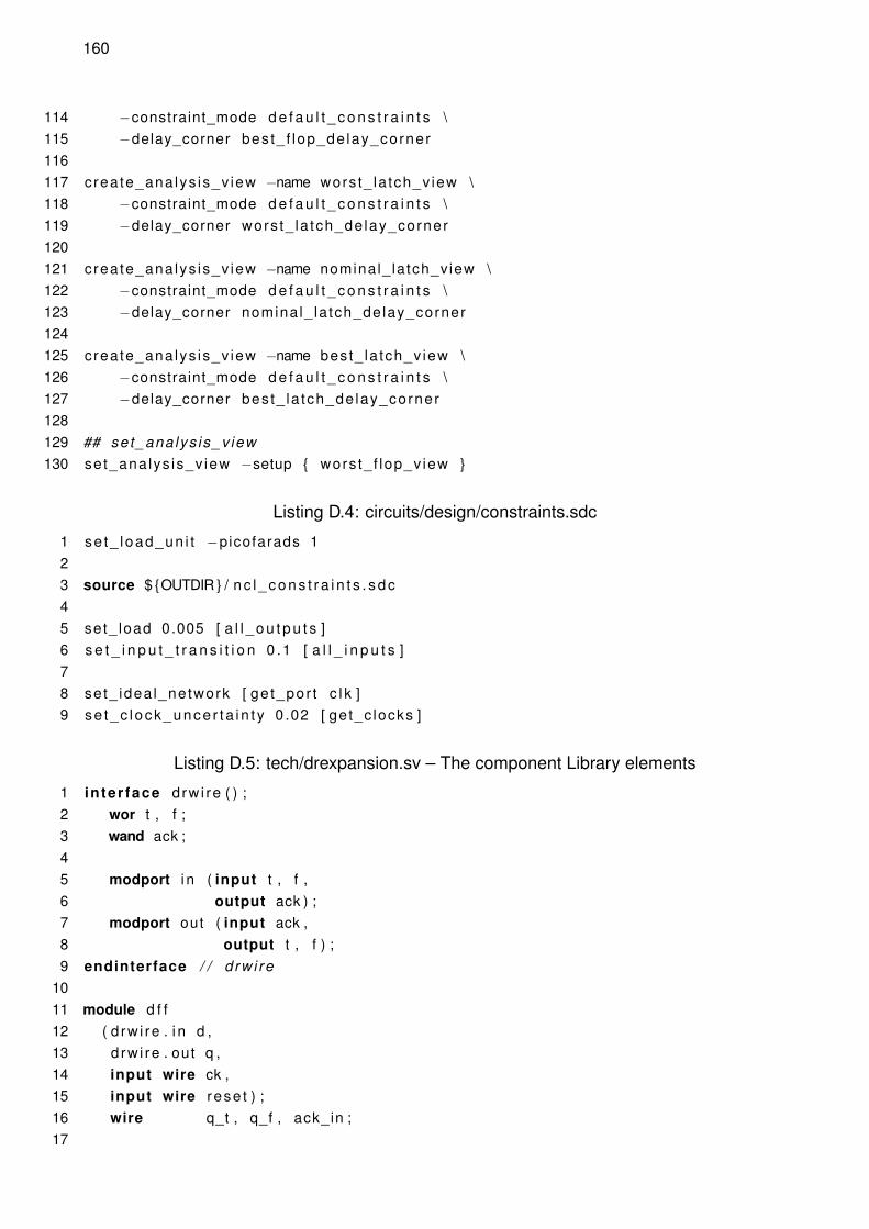
160
114 −constraint_mode d e f a u l t _ c o n s t r a i n t s \115 −delay_corner bes t_ f lop_de lay_corner116117 create_ana lys is_v iew −name wors t_ la tch_v iew \118 −constraint_mode d e f a u l t _ c o n s t r a i n t s \119 −delay_corner wors t_ la tch_de lay_corner120121 create_ana lys is_v iew −name nominal_ la tch_view \122 −constraint_mode d e f a u l t _ c o n s t r a i n t s \123 −delay_corner nomina l_ la tch_delay_corner124125 create_ana lys is_v iew −name best_ la tch_v iew \126 −constraint_mode d e f a u l t _ c o n s t r a i n t s \127 −delay_corner bes t_ la tch_de lay_corner128129 ## set_ana lys is_v iew130 set_ana lys is_v iew −setup { wors t_ f lop_v iew }
Listing D.4: circuits/design/constraints.sdc
1 se t_ load_un i t −picofarads 123 source $ {OUTDIR } / n c l _ c o n s t r a i n t s . s d c45 set_ load 0.005 [ a l l _ o u t p u t s ]6 s e t _ i n p u t _ t r a n s i t i o n 0 .1 [ a l l _ i n p u t s ]78 set_ idea l_network [ ge t_por t c l k ]9 se t_c lock_unce r ta i n t y 0 .02 [ get_c locks ]
Listing D.5: tech/drexpansion.sv – The component Library elements
1 in ter face drw i re ( ) ;2 wor t , f ;3 wand ack ;45 modport i n ( input t , f ,6 output ack ) ;7 modport out ( input ack ,8 output t , f ) ;9 endinterface / / d rw i re
1011 module d f f12 ( d rw i re . i n d ,13 drw i re . out q ,14 input wire ck ,15 input wire rese t ) ;16 wire q_t , q_f , ack_in ;17
161
18 SY_RNCL2W11OF2X9 f ( . A( d . f ) , .B( ack_in ) , .Q( q_f ) , .RN( rese t ) , .G( ck ) ) ;19 SY_RNCL2W11OF2X9 t ( . A( d . t ) , .B( ack_in ) , .Q( q_t ) , .RN( rese t ) , .G( ck ) ) ;2021 assign ack_in = ~(q . ack ) ;22 assign d . ack = q_t | q_f ;23 assign q . t = q_t ;24 assign q . f = q_f ;25 endmodule / / d f f2627 module d f f s_s lave28 ( d rw i re . i n d ,29 drw i re . out q ,30 input wire ck ,31 input wire rese t ) ;3233 wire ack_in , set , i n t _ t , i n t _ f ;3435 ST_SNCL2W11OF2X9 t ( . A( d . t ) , .B( ack_in ) , .Q( i n t _ t ) , .S( set ) , .G( ck ) ) ;36 SY_RNCL2W11OF2X9 f ( . A( d . f ) , .B( ack_in ) , .Q( i n t _ f ) , .RN( rese t ) , .G( ck ) ) ;3738 assign set = ~ rese t ;39 assign ack_in = ~(q . ack ) ;40 assign q . t = i n t _ t ;41 assign q . f = i n t _ f ;42 assign d . ack = i n t _ t | i n t _ f ;43 endmodule / / d f f s_s lave4445 module d f f s46 ( d rw i re . i n d ,47 drw i re . out q ,48 input wire ck ,49 input wire sb ) ;50 wire i n t _ t , i n t _ f , ack_in ;5152 drw i re out ( ) ;53 drw i re i n ( ) ;5455 SY_RNCL2W11OF2X9 t ( . A( d . t ) , .B( ack_in ) , .Q( i n t _ t ) , .RN( sb ) , .G( ck ) ) ;56 SY_RNCL2W11OF2X9 f ( . A( d . f ) , .B( ack_in ) , .Q( i n t _ f ) , .RN( sb ) , .G( ck ) ) ;5758 d f f sout ( . d ( out ) , . q ( q ) , . rese t ( sb ) , . ck ( ck ) ) ;59 d f f s_s lave s in ( . d ( i n ) , . q ( out ) , . rese t ( sb ) , . ck ( ck ) ) ;6061 assign i n . t = i n t _ t ;62 assign i n . f = i n t _ f ;63 assign ack_in = ~( i n . ack ) ;64 assign d . ack = i n t _ t | i n t _ f ;65 endmodule / / d f f r
162
6667 module d f f r _ s l a v e68 ( d rw i re . i n d ,69 drw i re . out q ,70 input wire ck ,71 input wire rese t ) ;7273 wire ack_in , set , i n t _ t , i n t _ f ;7475 SY_RNCL2W11OF2X9 t ( . A( d . t ) , .B( ack_in ) , .Q( i n t _ t ) , .RN( rese t ) , .G( ck ) ) ;76 ST_SNCL2W11OF2X9 f ( . A( d . f ) , .B( ack_in ) , .Q( i n t _ f ) , .S( set ) , .G( ck ) ) ;7778 assign set = ~ rese t ;79 assign ack_in = ~(q . ack ) ;80 assign q . t = i n t _ t ;81 assign q . f = i n t _ f ;82 assign d . ack = i n t _ t | i n t _ f ;83 endmodule ; / / d f f r _ s l a v e8485 module d f f r86 ( d rw i re . i n d ,87 drw i re . out q ,88 input wire ck ,89 input wire rb ) ;90 wire i n t _ t , i n t _ f , ack_in ;9192 drw i re out ( ) ;93 drw i re i n ( ) ;9495 SY_RNCL2W11OF2X9 t ( . A( d . t ) , .B( ack_in ) , .Q( i n t _ t ) , .RN( rb ) , .G( ck ) ) ;96 SY_RNCL2W11OF2X9 f ( . A( d . f ) , .B( ack_in ) , .Q( i n t _ f ) , .RN( rb ) , .G( ck ) ) ;9798 d f f sout ( . d ( out ) , . q ( q ) , . rese t ( rb ) , . ck ( ck ) ) ;99 d f f r _ s l a v e s in ( . d ( i n ) , . q ( out ) , . rese t ( rb ) , . ck ( ck ) ) ;
100101 assign i n . t = i n t _ t ;102 assign i n . f = i n t _ f ;103 assign ack_in = ~( i n . ack ) ;104 assign d . ack = i n t _ t | i n t _ f ;105 endmodule / / d f f r106107 module nand2108 ( d rw i re . i n a ,109 drw i re . i n b ,110 drw i re . out y ) ;111112 assign y . t = a . f & b . f |113 a . f & b . t |
163
114 a . t & b . f ;115116 assign y . f = a . t & b . t ;117 assign a . ack = y . ack ;118 assign b . ack = y . ack ;119 endmodule / / nand2120121 module nor2122 ( d rw i re . i n a ,123 drw i re . i n b ,124 drw i re . out y ) ;125126 assign y . f = a . t & b . t |127 a . t & b . f |128 a . f & b . t ;129130 assign y . t = a . f & b . f ;131 assign a . ack = y . ack ;132 assign b . ack = y . ack ;133 endmodule / / nor2134135 module xor2136 ( d rw i re . i n a ,137 drw i re . i n b ,138 drw i re . out y ) ;139140 assign y . t = a . t & b . f |141 a . f & b . t ;142143 assign y . f = a . f & b . f |144 a . t & b . t ;145146 assign a . ack = y . ack ;147 assign b . ack = y . ack ;148 endmodule / / xor2149150 module b u f f151 ( d rw i re . i n a ,152 drw i re . out y ) ;153154 assign y . t = a . t ;155 assign y . f = a . f ;156 assign a . ack = y . ack ;157 endmodule / / b u f f158159 module i nv160 ( d rw i re . i n a ,161 drw i re . out y ) ;

164
162163 assign y . t = a . f ;164 assign y . f = a . t ;165 assign a . ack = y . ack ;166 endmodule / / i nv
Listing D.6: tech/st65.tcl
1 set e q u i v a l e n t _ c e l l (ST_NCL1W111OF3X2) ST_NCLP3W111OF3X22 set e q u i v a l e n t _ c e l l (ST_NCLP3W111OF3X2) ST_NCL1W111OF3X23 set e q u i v a l e n t _ c e l l (ST_NCL1W111OF3X4) ST_NCLP3W111OF3X44 set e q u i v a l e n t _ c e l l (ST_NCLP3W111OF3X4) ST_NCL1W111OF3X45 set e q u i v a l e n t _ c e l l (ST_NCL1W111OF3X7) ST_NCLP3W111OF3X76 set e q u i v a l e n t _ c e l l (ST_NCLP3W111OF3X7) ST_NCL1W111OF3X77 set e q u i v a l e n t _ c e l l (ST_NCL1W111OF3X9) ST_NCLP3W111OF3X98 set e q u i v a l e n t _ c e l l (ST_NCLP3W111OF3X9) ST_NCL1W111OF3X99 set e q u i v a l e n t _ c e l l (ST_NCL1W111OF3X13) ST_NCLP3W111OF3X13
10 set e q u i v a l e n t _ c e l l (ST_NCLP3W111OF3X13) ST_NCL1W111OF3X1311 set e q u i v a l e n t _ c e l l (ST_NCL1W111OF3X18) ST_NCLP3W111OF3X1812 set e q u i v a l e n t _ c e l l (ST_NCLP3W111OF3X18) ST_NCL1W111OF3X1813 set e q u i v a l e n t _ c e l l (ST_INCL3W111OF3X2) ST_INCLP1W111OF3X214 set e q u i v a l e n t _ c e l l (ST_INCLP1W111OF3X2) ST_INCL3W111OF3X215 set e q u i v a l e n t _ c e l l (ST_INCL3W111OF3X4) ST_INCLP1W111OF3X416 set e q u i v a l e n t _ c e l l (ST_INCLP1W111OF3X4) ST_INCL3W111OF3X417 set e q u i v a l e n t _ c e l l (ST_INCL3W111OF3X7) ST_INCLP1W111OF3X718 set e q u i v a l e n t _ c e l l (ST_INCLP1W111OF3X7) ST_INCL3W111OF3X719 set e q u i v a l e n t _ c e l l (ST_INCL3W111OF3X9) ST_INCLP1W111OF3X920 set e q u i v a l e n t _ c e l l (ST_INCLP1W111OF3X9) ST_INCL3W111OF3X921 set e q u i v a l e n t _ c e l l (ST_INCL3W111OF3X13) ST_INCLP1W111OF3X1322 set e q u i v a l e n t _ c e l l (ST_INCLP1W111OF3X13) ST_INCL3W111OF3X1323 set e q u i v a l e n t _ c e l l (ST_INCL3W111OF3X18) ST_INCLP1W111OF3X1824 set e q u i v a l e n t _ c e l l (ST_INCLP1W111OF3X18) ST_INCL3W111OF3X1825 set e q u i v a l e n t _ c e l l (ST_INCL3W111OF3X31) ST_INCLP1W111OF3X1826 set e q u i v a l e n t _ c e l l (ST_INCL4W2211OF4X2) ST_INCLP3W2211OF4X227 set e q u i v a l e n t _ c e l l (ST_INCLP3W2211OF4X2) ST_INCL4W2211OF4X228 set e q u i v a l e n t _ c e l l (ST_INCL4W2211OF4X4) ST_INCLP3W2211OF4X429 set e q u i v a l e n t _ c e l l (ST_INCLP3W2211OF4X4) ST_INCL4W2211OF4X430 set e q u i v a l e n t _ c e l l (ST_INCL4W2211OF4X7) ST_INCLP3W2211OF4X731 set e q u i v a l e n t _ c e l l (ST_INCLP3W2211OF4X7) ST_INCL4W2211OF4X732 set e q u i v a l e n t _ c e l l (ST_INCL4W2211OF4X9) ST_INCLP3W2211OF4X1333 set e q u i v a l e n t _ c e l l (ST_INCLP3W2211OF4X13) ST_INCL4W2211OF4X934 set e q u i v a l e n t _ c e l l (ST_INCL3W2111OF4X2) ST_INCLP3W2111OF4X235 set e q u i v a l e n t _ c e l l (ST_INCLP3W2111OF4X2) ST_INCL3W2111OF4X236 set e q u i v a l e n t _ c e l l (ST_INCL3W2111OF4X4) ST_INCLP3W2111OF4X437 set e q u i v a l e n t _ c e l l (ST_INCLP3W2111OF4X4) ST_INCL3W2111OF4X438 set e q u i v a l e n t _ c e l l (ST_INCL3W2111OF4X7) ST_INCLP3W2111OF4X739 set e q u i v a l e n t _ c e l l (ST_INCLP3W2111OF4X7) ST_INCL3W2111OF4X740 set e q u i v a l e n t _ c e l l (ST_INCL3W2111OF4X9) ST_INCLP3W2111OF4X9

165
41 set e q u i v a l e n t _ c e l l (ST_INCLP3W2111OF4X9) ST_INCL3W2111OF4X942 set e q u i v a l e n t _ c e l l (ST_INCL3W2111OF4X13) ST_INCLP3W2111OF4X1343 set e q u i v a l e n t _ c e l l (ST_INCLP3W2111OF4X13) ST_INCL3W2111OF4X1344 set e q u i v a l e n t _ c e l l (ST_NCLAO21O2OF4X2) ST_NCLPAO2O21OF4X245 set e q u i v a l e n t _ c e l l (ST_NCLPAO2O21OF4X2) ST_NCLAO21O2OF4X246 set e q u i v a l e n t _ c e l l (ST_NCLAO21O2OF4X4) ST_NCLPAO2O21OF4X447 set e q u i v a l e n t _ c e l l (ST_NCLPAO2O21OF4X4) ST_NCLAO21O2OF4X448 set e q u i v a l e n t _ c e l l (ST_NCLAO21O2OF4X7) ST_NCLPAO2O21OF4X749 set e q u i v a l e n t _ c e l l (ST_NCLPAO2O21OF4X7) ST_NCLAO21O2OF4X750 set e q u i v a l e n t _ c e l l (ST_NCLAO21O2OF4X9) ST_NCLPAO2O21OF4X951 set e q u i v a l e n t _ c e l l (ST_NCLPAO2O21OF4X9) ST_NCLAO21O2OF4X952 set e q u i v a l e n t _ c e l l (ST_NCLAO21O2OF4X13) ST_NCLPAO2O21OF4X1353 set e q u i v a l e n t _ c e l l (ST_NCLPAO2O21OF4X13) ST_NCLAO21O2OF4X1354 set e q u i v a l e n t _ c e l l (ST_NCL4W3221OF4X2) ST_NCLP5W3221OF4X255 set e q u i v a l e n t _ c e l l (ST_NCLP5W3221OF4X2) ST_NCL4W3221OF4X256 set e q u i v a l e n t _ c e l l (ST_NCL4W3221OF4X4) ST_NCLP5W3221OF4X457 set e q u i v a l e n t _ c e l l (ST_NCLP5W3221OF4X4) ST_NCL4W3221OF4X458 set e q u i v a l e n t _ c e l l (ST_NCLP5W3221OF4X7) ST_NCL4W3221OF4X959 set e q u i v a l e n t _ c e l l (ST_NCL4W3221OF4X9) ST_NCLP5W3221OF4X960 set e q u i v a l e n t _ c e l l (ST_NCLP5W3221OF4X9) ST_NCL4W3221OF4X961 set e q u i v a l e n t _ c e l l (ST_NCL4W3221OF4X13) ST_NCLP5W3221OF4X1362 set e q u i v a l e n t _ c e l l (ST_NCLP5W3221OF4X13) ST_NCL4W3221OF4X1363 set e q u i v a l e n t _ c e l l (ST_INCL3W2211OF4X2) ST_INCLP4W2211OF4X464 set e q u i v a l e n t _ c e l l (ST_INCL3W2211OF4X4) ST_INCLP4W2211OF4X465 set e q u i v a l e n t _ c e l l (ST_INCLP4W2211OF4X4) ST_INCL3W2211OF4X466 set e q u i v a l e n t _ c e l l (ST_INCL3W2211OF4X7) ST_INCLP4W2211OF4X767 set e q u i v a l e n t _ c e l l (ST_INCLP4W2211OF4X7) ST_INCL3W2211OF4X768 set e q u i v a l e n t _ c e l l (ST_INCL3W2211OF4X9) ST_INCLP4W2211OF4X969 set e q u i v a l e n t _ c e l l (ST_INCLP4W2211OF4X9) ST_INCL3W2211OF4X970 set e q u i v a l e n t _ c e l l (ST_INCLP4W2211OF4X13) ST_INCL3W2211OF4X971 set e q u i v a l e n t _ c e l l (ST_INCL1W1111OF4X2) ST_INCLP4W1111OF4X272 set e q u i v a l e n t _ c e l l (ST_INCLP4W1111OF4X2) ST_INCL1W1111OF4X273 set e q u i v a l e n t _ c e l l (ST_INCL1W1111OF4X4) ST_INCLP4W1111OF4X474 set e q u i v a l e n t _ c e l l (ST_INCLP4W1111OF4X4) ST_INCL1W1111OF4X475 set e q u i v a l e n t _ c e l l (ST_INCL1W1111OF4X7) ST_INCLP4W1111OF4X776 set e q u i v a l e n t _ c e l l (ST_INCLP4W1111OF4X7) ST_INCL1W1111OF4X777 set e q u i v a l e n t _ c e l l (ST_INCL1W1111OF4X9) ST_INCLP4W1111OF4X978 set e q u i v a l e n t _ c e l l (ST_INCLP4W1111OF4X9) ST_INCL1W1111OF4X979 set e q u i v a l e n t _ c e l l (ST_INCL1W1111OF4X13) ST_INCLP4W1111OF4X980 set e q u i v a l e n t _ c e l l (ST_INCL1W1111OF4X18) ST_INCLP4W1111OF4X981 set e q u i v a l e n t _ c e l l (ST_INCL1W1111OF4X31) ST_INCLP4W1111OF4X982 set e q u i v a l e n t _ c e l l (ST_NCL2W1111OF4X2) ST_NCLP3W1111OF4X283 set e q u i v a l e n t _ c e l l (ST_NCLP3W1111OF4X2) ST_NCL2W1111OF4X284 set e q u i v a l e n t _ c e l l (ST_NCL2W1111OF4X4) ST_NCLP3W1111OF4X485 set e q u i v a l e n t _ c e l l (ST_NCLP3W1111OF4X4) ST_NCL2W1111OF4X486 set e q u i v a l e n t _ c e l l (ST_NCL2W1111OF4X7) ST_NCLP3W1111OF4X787 set e q u i v a l e n t _ c e l l (ST_NCLP3W1111OF4X7) ST_NCL2W1111OF4X788 set e q u i v a l e n t _ c e l l (ST_NCL2W1111OF4X9) ST_NCLP3W1111OF4X9
166
89 set e q u i v a l e n t _ c e l l (ST_NCLP3W1111OF4X9) ST_NCL2W1111OF4X990 set e q u i v a l e n t _ c e l l (ST_NCL2W1111OF4X13) ST_NCLP3W1111OF4X1391 set e q u i v a l e n t _ c e l l (ST_NCLP3W1111OF4X13) ST_NCL2W1111OF4X1392 set e q u i v a l e n t _ c e l l (ST_NCL5W3221OF4X2) ST_NCLP4W3221OF4X293 set e q u i v a l e n t _ c e l l (ST_NCLP4W3221OF4X2) ST_NCL5W3221OF4X294 set e q u i v a l e n t _ c e l l (ST_NCL5W3221OF4X4) ST_NCLP4W3221OF4X495 set e q u i v a l e n t _ c e l l (ST_NCLP4W3221OF4X4) ST_NCL5W3221OF4X496 set e q u i v a l e n t _ c e l l (ST_NCL5W3221OF4X7) ST_NCLP4W3221OF4X797 set e q u i v a l e n t _ c e l l (ST_NCLP4W3221OF4X7) ST_NCL5W3221OF4X798 set e q u i v a l e n t _ c e l l (ST_NCL5W3221OF4X9) ST_NCLP4W3221OF4X999 set e q u i v a l e n t _ c e l l (ST_NCLP4W3221OF4X9) ST_NCL5W3221OF4X9
100 set e q u i v a l e n t _ c e l l (ST_NCL5W3221OF4X13) ST_NCLP4W3221OF4X13101 set e q u i v a l e n t _ c e l l (ST_NCLP4W3221OF4X13) ST_NCL5W3221OF4X13102 set e q u i v a l e n t _ c e l l (ST_NCL3W3111OF4X2) ST_NCLP4W3111OF4X2103 set e q u i v a l e n t _ c e l l (ST_NCLP4W3111OF4X2) ST_NCL3W3111OF4X2104 set e q u i v a l e n t _ c e l l (ST_NCL3W3111OF4X4) ST_NCLP4W3111OF4X4105 set e q u i v a l e n t _ c e l l (ST_NCLP4W3111OF4X4) ST_NCL3W3111OF4X4106 set e q u i v a l e n t _ c e l l (ST_NCL3W3111OF4X7) ST_NCLP4W3111OF4X9107 set e q u i v a l e n t _ c e l l (ST_NCL3W3111OF4X9) ST_NCLP4W3111OF4X9108 set e q u i v a l e n t _ c e l l (ST_NCLP4W3111OF4X9) ST_NCL3W3111OF4X9109 set e q u i v a l e n t _ c e l l (ST_NCL3W3111OF4X13) ST_NCLP4W3111OF4X13110 set e q u i v a l e n t _ c e l l (ST_NCLP4W3111OF4X13) ST_NCL3W3111OF4X13111 set e q u i v a l e n t _ c e l l (ST_INCL4W1111OF4X2) ST_INCLP1W1111OF4X2112 set e q u i v a l e n t _ c e l l (ST_INCLP1W1111OF4X2) ST_INCL4W1111OF4X2113 set e q u i v a l e n t _ c e l l (ST_INCL4W1111OF4X4) ST_INCLP1W1111OF4X4114 set e q u i v a l e n t _ c e l l (ST_INCLP1W1111OF4X4) ST_INCL4W1111OF4X4115 set e q u i v a l e n t _ c e l l (ST_INCL4W1111OF4X7) ST_INCLP1W1111OF4X7116 set e q u i v a l e n t _ c e l l (ST_INCLP1W1111OF4X7) ST_INCL4W1111OF4X7117 set e q u i v a l e n t _ c e l l (ST_INCL4W1111OF4X9) ST_INCLP1W1111OF4X9118 set e q u i v a l e n t _ c e l l (ST_INCLP1W1111OF4X9) ST_INCL4W1111OF4X9119 set e q u i v a l e n t _ c e l l (ST_INCLP1W1111OF4X13) ST_INCL4W1111OF4X9120 set e q u i v a l e n t _ c e l l (ST_INCLP1W1111OF4X18) ST_INCL4W1111OF4X9121 set e q u i v a l e n t _ c e l l (ST_NCL3W211OF3X2) ST_NCLP2W211OF3X2122 set e q u i v a l e n t _ c e l l (ST_NCLP2W211OF3X2) ST_NCL3W211OF3X2123 set e q u i v a l e n t _ c e l l (ST_NCL3W211OF3X4) ST_NCLP2W211OF3X4124 set e q u i v a l e n t _ c e l l (ST_NCLP2W211OF3X4) ST_NCL3W211OF3X4125 set e q u i v a l e n t _ c e l l (ST_NCL3W211OF3X7) ST_NCLP2W211OF3X7126 set e q u i v a l e n t _ c e l l (ST_NCLP2W211OF3X7) ST_NCL3W211OF3X7127 set e q u i v a l e n t _ c e l l (ST_NCL3W211OF3X9) ST_NCLP2W211OF3X9128 set e q u i v a l e n t _ c e l l (ST_NCLP2W211OF3X9) ST_NCL3W211OF3X9129 set e q u i v a l e n t _ c e l l (ST_NCL3W211OF3X13) ST_NCLP2W211OF3X13130 set e q u i v a l e n t _ c e l l (ST_NCLP2W211OF3X13) ST_NCL3W211OF3X13131 set e q u i v a l e n t _ c e l l (ST_NCL3W211OF3X18) ST_NCLP2W211OF3X18132 set e q u i v a l e n t _ c e l l (ST_NCLP2W211OF3X18) ST_NCL3W211OF3X18133 set e q u i v a l e n t _ c e l l (ST_NCL2W211OF3X2) ST_NCLP3W211OF3X2134 set e q u i v a l e n t _ c e l l (ST_NCLP3W211OF3X2) ST_NCL2W211OF3X2135 set e q u i v a l e n t _ c e l l (ST_NCL2W211OF3X4) ST_NCLP3W211OF3X4136 set e q u i v a l e n t _ c e l l (ST_NCLP3W211OF3X4) ST_NCL2W211OF3X4
167
137 set e q u i v a l e n t _ c e l l (ST_NCL2W211OF3X7) ST_NCLP3W211OF3X7138 set e q u i v a l e n t _ c e l l (ST_NCLP3W211OF3X7) ST_NCL2W211OF3X7139 set e q u i v a l e n t _ c e l l (ST_NCL2W211OF3X9) ST_NCLP3W211OF3X9140 set e q u i v a l e n t _ c e l l (ST_NCLP3W211OF3X9) ST_NCL2W211OF3X9141 set e q u i v a l e n t _ c e l l (ST_NCL2W211OF3X13) ST_NCLP3W211OF3X13142 set e q u i v a l e n t _ c e l l (ST_NCLP3W211OF3X13) ST_NCL2W211OF3X13143 set e q u i v a l e n t _ c e l l (ST_NCLP3W211OF3X18) ST_NCL2W211OF3X13144 set e q u i v a l e n t _ c e l l (ST_INCL1W11OF2X2) SY_INCLP2W11OF2X2145 set e q u i v a l e n t _ c e l l (SY_INCLP2W11OF2X2) ST_INCL1W11OF2X4146 set e q u i v a l e n t _ c e l l (ST_INCL1W11OF2X4) ST_INCLP2W11OF2X4147 set e q u i v a l e n t _ c e l l (ST_INCLP2W11OF2X4) ST_INCL1W11OF2X4148 set e q u i v a l e n t _ c e l l (SY_INCLP2W11OF2X4) ST_INCL1W11OF2X7149 set e q u i v a l e n t _ c e l l (ST_INCL1W11OF2X7) ST_INCLP2W11OF2X7150 set e q u i v a l e n t _ c e l l (ST_INCLP2W11OF2X7) ST_INCL1W11OF2X7151 set e q u i v a l e n t _ c e l l (SY_INCLP2W11OF2X7) ST_INCL1W11OF2X9152 set e q u i v a l e n t _ c e l l (ST_INCL1W11OF2X9) SY_INCLP2W11OF2X9153 set e q u i v a l e n t _ c e l l (SY_INCLP2W11OF2X9) ST_INCL1W11OF2X13154 set e q u i v a l e n t _ c e l l (ST_INCL1W11OF2X13) ST_INCLP2W11OF2X13155 set e q u i v a l e n t _ c e l l (ST_INCLP2W11OF2X13) ST_INCL1W11OF2X13156 set e q u i v a l e n t _ c e l l (SY_INCLP2W11OF2X13) ST_INCL1W11OF2X18157 set e q u i v a l e n t _ c e l l (ST_INCL1W11OF2X18) ST_INCLP2W11OF2X18158 set e q u i v a l e n t _ c e l l (ST_INCLP2W11OF2X18) ST_INCL1W11OF2X18159 set e q u i v a l e n t _ c e l l (SY_INCLP2W11OF2X18) ST_INCL1W11OF2X18160 set e q u i v a l e n t _ c e l l (ST_INCLP2W11OF2X22) ST_INCL1W11OF2X18161 set e q u i v a l e n t _ c e l l (ST_INCLP2W11OF2X31) ST_INCL1W11OF2X18162 set e q u i v a l e n t _ c e l l (ST_INCL3W211OF3X2) ST_INCLP2W211OF3X2163 set e q u i v a l e n t _ c e l l (ST_INCLP2W211OF3X2) ST_INCL3W211OF3X2164 set e q u i v a l e n t _ c e l l (ST_INCL3W211OF3X4) ST_INCLP2W211OF3X4165 set e q u i v a l e n t _ c e l l (ST_INCLP2W211OF3X4) ST_INCL3W211OF3X4166 set e q u i v a l e n t _ c e l l (ST_INCL3W211OF3X7) ST_INCLP2W211OF3X7167 set e q u i v a l e n t _ c e l l (ST_INCLP2W211OF3X7) ST_INCL3W211OF3X7168 set e q u i v a l e n t _ c e l l (ST_INCL3W211OF3X9) ST_INCLP2W211OF3X9169 set e q u i v a l e n t _ c e l l (ST_INCLP2W211OF3X9) ST_INCL3W211OF3X9170 set e q u i v a l e n t _ c e l l (ST_INCL3W211OF3X13) ST_INCLP2W211OF3X18171 set e q u i v a l e n t _ c e l l (ST_INCL3W211OF3X18) ST_INCLP2W211OF3X18172 set e q u i v a l e n t _ c e l l (ST_INCLP2W211OF3X18) ST_INCL3W211OF3X18173 set e q u i v a l e n t _ c e l l (ST_INCLP2W211OF3X22) ST_INCL3W211OF3X31174 set e q u i v a l e n t _ c e l l (ST_INCLP2W211OF3X27) ST_INCL3W211OF3X31175 set e q u i v a l e n t _ c e l l (ST_INCL3W211OF3X31) ST_INCLP2W211OF3X27176 set e q u i v a l e n t _ c e l l (ST_NCL2W11OF2X2) ST_NCLP1W11OF2X2177 set e q u i v a l e n t _ c e l l (ST_NCLP1W11OF2X2) ST_NCL2W11OF2X2178 set e q u i v a l e n t _ c e l l (SY_NCL2W11OF2X2) ST_NCLP1W11OF2X4179 set e q u i v a l e n t _ c e l l (ST_NCL2W11OF2X4) ST_NCLP1W11OF2X4180 set e q u i v a l e n t _ c e l l (ST_NCLP1W11OF2X4) ST_NCL2W11OF2X4181 set e q u i v a l e n t _ c e l l (SY_NCL2W11OF2X4) ST_NCLP1W11OF2X7182 set e q u i v a l e n t _ c e l l (ST_NCL2W11OF2X7) ST_NCLP1W11OF2X7183 set e q u i v a l e n t _ c e l l (ST_NCLP1W11OF2X7) ST_NCL2W11OF2X7184 set e q u i v a l e n t _ c e l l (ST_NCL2W11OF2X9) ST_NCLP1W11OF2X9
168
185 set e q u i v a l e n t _ c e l l (ST_NCLP1W11OF2X9) ST_NCL2W11OF2X9186 set e q u i v a l e n t _ c e l l (SY_NCL2W11OF2X9) ST_NCLP1W11OF2X13187 set e q u i v a l e n t _ c e l l (ST_NCL2W11OF2X13) ST_NCLP1W11OF2X13188 set e q u i v a l e n t _ c e l l (ST_NCLP1W11OF2X13) ST_NCL2W11OF2X13189 set e q u i v a l e n t _ c e l l (SY_NCL2W11OF2X13) ST_NCLP1W11OF2X18190 set e q u i v a l e n t _ c e l l (ST_NCLP1W11OF2X18) SY_NCL2W11OF2X18191 set e q u i v a l e n t _ c e l l (SY_NCL2W11OF2X18) ST_NCLP1W11OF2X18192 set e q u i v a l e n t _ c e l l (ST_NCL4W1111OF4X2) ST_NCLP1W1111OF4X2193 set e q u i v a l e n t _ c e l l (ST_NCLP1W1111OF4X2) ST_NCL4W1111OF4X2194 set e q u i v a l e n t _ c e l l (ST_NCL4W1111OF4X4) ST_NCLP1W1111OF4X4195 set e q u i v a l e n t _ c e l l (ST_NCLP1W1111OF4X4) ST_NCL4W1111OF4X4196 set e q u i v a l e n t _ c e l l (ST_NCL4W1111OF4X7) ST_NCLP1W1111OF4X7197 set e q u i v a l e n t _ c e l l (ST_NCLP1W1111OF4X7) ST_NCL4W1111OF4X7198 set e q u i v a l e n t _ c e l l (ST_NCL4W1111OF4X9) ST_NCLP1W1111OF4X13199 set e q u i v a l e n t _ c e l l (ST_NCL4W1111OF4X13) ST_NCLP1W1111OF4X13200 set e q u i v a l e n t _ c e l l (ST_NCLP1W1111OF4X13) ST_NCL4W1111OF4X13201 set e q u i v a l e n t _ c e l l (ST_NCLP1W1111OF4X18) ST_NCL4W1111OF4X13202 set e q u i v a l e n t _ c e l l (ST_INCL5W2211OF4X2) ST_INCLP2W2211OF4X2203 set e q u i v a l e n t _ c e l l (ST_INCLP2W2211OF4X2) ST_INCL5W2211OF4X2204 set e q u i v a l e n t _ c e l l (ST_INCL5W2211OF4X4) ST_INCLP2W2211OF4X4205 set e q u i v a l e n t _ c e l l (ST_INCLP2W2211OF4X4) ST_INCL5W2211OF4X4206 set e q u i v a l e n t _ c e l l (ST_INCL5W2211OF4X7) ST_INCLP2W2211OF4X7207 set e q u i v a l e n t _ c e l l (ST_INCLP2W2211OF4X7) ST_INCL5W2211OF4X7208 set e q u i v a l e n t _ c e l l (ST_INCL5W2211OF4X9) ST_INCLP2W2211OF4X9209 set e q u i v a l e n t _ c e l l (ST_INCLP2W2211OF4X9) ST_INCL5W2211OF4X9210 set e q u i v a l e n t _ c e l l (ST_INCL5W2211OF4X13) ST_INCLP2W2211OF4X13211 set e q u i v a l e n t _ c e l l (ST_INCLP2W2211OF4X13) ST_INCL5W2211OF4X13212 set e q u i v a l e n t _ c e l l (ST_INCL5W2211OF4X18) ST_INCLP2W2211OF4X18213 set e q u i v a l e n t _ c e l l (ST_INCLP2W2211OF4X18) ST_INCL5W2211OF4X18214 set e q u i v a l e n t _ c e l l (ST_INCL5W2211OF4X22) ST_INCLP2W2211OF4X18215 set e q u i v a l e n t _ c e l l (ST_INCL2W2211OF4X2) ST_INCLP5W2211OF4X2216 set e q u i v a l e n t _ c e l l (ST_INCLP5W2211OF4X2) ST_INCL2W2211OF4X2217 set e q u i v a l e n t _ c e l l (ST_INCL2W2211OF4X4) ST_INCLP5W2211OF4X4218 set e q u i v a l e n t _ c e l l (ST_INCLP5W2211OF4X4) ST_INCL2W2211OF4X4219 set e q u i v a l e n t _ c e l l (ST_INCL2W2211OF4X7) ST_INCLP5W2211OF4X7220 set e q u i v a l e n t _ c e l l (ST_INCLP5W2211OF4X7) ST_INCL2W2211OF4X7221 set e q u i v a l e n t _ c e l l (ST_INCL2W2211OF4X9) ST_INCLP5W2211OF4X9222 set e q u i v a l e n t _ c e l l (ST_INCLP5W2211OF4X9) ST_INCL2W2211OF4X9223 set e q u i v a l e n t _ c e l l (ST_INCL2W2211OF4X13) ST_INCLP5W2211OF4X13224 set e q u i v a l e n t _ c e l l (ST_INCLP5W2211OF4X13) ST_INCL2W2211OF4X13225 set e q u i v a l e n t _ c e l l (ST_INCL2W2211OF4X18) ST_INCLP5W2211OF4X13226 set e q u i v a l e n t _ c e l l (ST_INCL2W2211OF4X31) ST_INCLP5W2211OF4X13227 set e q u i v a l e n t _ c e l l (ST_INCL5W3221OF4X2) ST_INCLP4W3221OF4X2228 set e q u i v a l e n t _ c e l l (ST_INCLP4W3221OF4X2) ST_INCL5W3221OF4X2229 set e q u i v a l e n t _ c e l l (ST_INCL5W3221OF4X4) ST_INCLP4W3221OF4X4230 set e q u i v a l e n t _ c e l l (ST_INCLP4W3221OF4X4) ST_INCL5W3221OF4X4231 set e q u i v a l e n t _ c e l l (ST_INCL5W3221OF4X7) ST_INCLP4W3221OF4X7232 set e q u i v a l e n t _ c e l l (ST_INCLP4W3221OF4X7) ST_INCL5W3221OF4X7

169
233 set e q u i v a l e n t _ c e l l (ST_INCLP4W3221OF4X9) ST_INCL5W3221OF4X7234 set e q u i v a l e n t _ c e l l (ST_INCLP4W3221OF4X13) ST_INCL5W3221OF4X7235 set e q u i v a l e n t _ c e l l (ST_NCLAO22OF4X2) ST_NCLPOA22OF4X4236 set e q u i v a l e n t _ c e l l (ST_NCLAO22OF4X4) ST_NCLPOA22OF4X4237 set e q u i v a l e n t _ c e l l (ST_NCLPOA22OF4X4) ST_NCLAO22OF4X4238 set e q u i v a l e n t _ c e l l (ST_NCLAO22OF4X7) ST_NCLPOA22OF4X7239 set e q u i v a l e n t _ c e l l (ST_NCLPOA22OF4X7) ST_NCLAO22OF4X7240 set e q u i v a l e n t _ c e l l (ST_NCLAO22OF4X9) ST_NCLPOA22OF4X9241 set e q u i v a l e n t _ c e l l (ST_NCLPOA22OF4X9) ST_NCLAO22OF4X9242 set e q u i v a l e n t _ c e l l (ST_NCLAO22OF4X13) ST_NCLPOA22OF4X13243 set e q u i v a l e n t _ c e l l (ST_NCLPOA22OF4X13) ST_NCLAO22OF4X13244 set e q u i v a l e n t _ c e l l (ST_INCL4W2111OF4X2) ST_INCLP2W2111OF4X2245 set e q u i v a l e n t _ c e l l (ST_INCLP2W2111OF4X2) ST_INCL4W2111OF4X2246 set e q u i v a l e n t _ c e l l (ST_INCL4W2111OF4X4) ST_INCLP2W2111OF4X4247 set e q u i v a l e n t _ c e l l (ST_INCLP2W2111OF4X4) ST_INCL4W2111OF4X4248 set e q u i v a l e n t _ c e l l (ST_INCL4W2111OF4X7) ST_INCLP2W2111OF4X7249 set e q u i v a l e n t _ c e l l (ST_INCLP2W2111OF4X7) ST_INCL4W2111OF4X7250 set e q u i v a l e n t _ c e l l (ST_INCL4W2111OF4X9) ST_INCLP2W2111OF4X9251 set e q u i v a l e n t _ c e l l (ST_INCLP2W2111OF4X9) ST_INCL4W2111OF4X9252 set e q u i v a l e n t _ c e l l (ST_INCL4W2111OF4X13) ST_INCLP2W2111OF4X9253 set e q u i v a l e n t _ c e l l (ST_NCL4W2211OF4X2) ST_NCLP3W2211OF4X2254 set e q u i v a l e n t _ c e l l (ST_NCLP3W2211OF4X2) ST_NCL4W2211OF4X2255 set e q u i v a l e n t _ c e l l (ST_NCLP3W2211OF4X4) ST_NCL4W2211OF4X7256 set e q u i v a l e n t _ c e l l (ST_NCL4W2211OF4X7) ST_NCLP3W2211OF4X4257 set e q u i v a l e n t _ c e l l (ST_NCL4W2211OF4X9) ST_NCLP3W2211OF4X13258 set e q u i v a l e n t _ c e l l (ST_NCL4W2211OF4X13) ST_NCLP3W2211OF4X13259 set e q u i v a l e n t _ c e l l (ST_NCLP3W2211OF4X13) ST_NCL4W2211OF4X13260 set e q u i v a l e n t _ c e l l (ST_INCL3W3111OF4X2) ST_INCLP4W3111OF4X2261 set e q u i v a l e n t _ c e l l (ST_INCLP4W3111OF4X2) ST_INCL3W3111OF4X2262 set e q u i v a l e n t _ c e l l (ST_INCL3W3111OF4X4) ST_INCLP4W3111OF4X4263 set e q u i v a l e n t _ c e l l (ST_INCLP4W3111OF4X4) ST_INCL3W3111OF4X4264 set e q u i v a l e n t _ c e l l (ST_INCL3W3111OF4X7) ST_INCLP4W3111OF4X7265 set e q u i v a l e n t _ c e l l (ST_INCLP4W3111OF4X7) ST_INCL3W3111OF4X7266 set e q u i v a l e n t _ c e l l (ST_INCL3W3111OF4X9) ST_INCLP4W3111OF4X9267 set e q u i v a l e n t _ c e l l (ST_INCLP4W3111OF4X9) ST_INCL3W3111OF4X9268 set e q u i v a l e n t _ c e l l (ST_INCL3W3111OF4X13) ST_INCLP4W3111OF4X9269 set e q u i v a l e n t _ c e l l (ST_INCL3W3111OF4X18) ST_INCLP4W3111OF4X9270 set e q u i v a l e n t _ c e l l (ST_INCL3W3111OF4X31) ST_INCLP4W3111OF4X9271 set e q u i v a l e n t _ c e l l (ST_NCL2W2211OF4X2) ST_NCLP5W2211OF4X2272 set e q u i v a l e n t _ c e l l (ST_NCLP5W2211OF4X2) ST_NCL2W2211OF4X2273 set e q u i v a l e n t _ c e l l (ST_NCL2W2211OF4X4) ST_NCLP5W2211OF4X4274 set e q u i v a l e n t _ c e l l (ST_NCLP5W2211OF4X4) ST_NCL2W2211OF4X4275 set e q u i v a l e n t _ c e l l (ST_NCL2W2211OF4X7) ST_NCLP5W2211OF4X7276 set e q u i v a l e n t _ c e l l (ST_NCLP5W2211OF4X7) ST_NCL2W2211OF4X7277 set e q u i v a l e n t _ c e l l (ST_NCL2W2211OF4X9) ST_NCLP5W2211OF4X9278 set e q u i v a l e n t _ c e l l (ST_NCLP5W2211OF4X9) ST_NCL2W2211OF4X9279 set e q u i v a l e n t _ c e l l (ST_NCL2W2211OF4X13) ST_NCLP5W2211OF4X13280 set e q u i v a l e n t _ c e l l (ST_NCLP5W2211OF4X13) ST_NCL2W2211OF4X13

170
281 set e q u i v a l e n t _ c e l l (ST_INCL2W1111OF4X2) ST_INCLP3W1111OF4X2282 set e q u i v a l e n t _ c e l l (ST_INCLP3W1111OF4X2) ST_INCL2W1111OF4X2283 set e q u i v a l e n t _ c e l l (ST_INCL2W1111OF4X4) ST_INCLP3W1111OF4X4284 set e q u i v a l e n t _ c e l l (ST_INCLP3W1111OF4X4) ST_INCL2W1111OF4X4285 set e q u i v a l e n t _ c e l l (ST_INCL2W1111OF4X7) ST_INCLP3W1111OF4X9286 set e q u i v a l e n t _ c e l l (ST_INCLP3W1111OF4X9) ST_INCL2W1111OF4X13287 set e q u i v a l e n t _ c e l l (ST_INCL2W1111OF4X13) ST_INCLP3W1111OF4X9288 set e q u i v a l e n t _ c e l l (ST_NCL3W111OF3X2) ST_NCLP1W111OF3X2289 set e q u i v a l e n t _ c e l l (ST_NCLP1W111OF3X2) ST_NCL3W111OF3X2290 set e q u i v a l e n t _ c e l l (ST_NCL3W111OF3X4) ST_NCLP1W111OF3X4291 set e q u i v a l e n t _ c e l l (ST_NCLP1W111OF3X4) ST_NCL3W111OF3X4292 set e q u i v a l e n t _ c e l l (ST_NCL3W111OF3X7) ST_NCLP1W111OF3X7293 set e q u i v a l e n t _ c e l l (ST_NCLP1W111OF3X7) ST_NCL3W111OF3X7294 set e q u i v a l e n t _ c e l l (ST_NCL3W111OF3X9) ST_NCLP1W111OF3X9295 set e q u i v a l e n t _ c e l l (ST_NCLP1W111OF3X9) ST_NCL3W111OF3X9296 set e q u i v a l e n t _ c e l l (ST_NCL3W111OF3X13) ST_NCLP1W111OF3X13297 set e q u i v a l e n t _ c e l l (ST_NCLP1W111OF3X13) ST_NCL3W111OF3X13298 set e q u i v a l e n t _ c e l l (ST_NCL3W111OF3X18) ST_NCLP1W111OF3X18299 set e q u i v a l e n t _ c e l l (ST_NCLP1W111OF3X18) ST_NCL3W111OF3X18300 set e q u i v a l e n t _ c e l l (ST_NCL3W2211OF4X2) ST_NCLP4W2211OF4X2301 set e q u i v a l e n t _ c e l l (ST_NCLP4W2211OF4X2) ST_NCL3W2211OF4X2302 set e q u i v a l e n t _ c e l l (ST_NCL3W2211OF4X4) ST_NCLP4W2211OF4X4303 set e q u i v a l e n t _ c e l l (ST_NCLP4W2211OF4X4) ST_NCL3W2211OF4X4304 set e q u i v a l e n t _ c e l l (ST_NCL3W2211OF4X7) ST_NCLP4W2211OF4X7305 set e q u i v a l e n t _ c e l l (ST_NCLP4W2211OF4X7) ST_NCL3W2211OF4X7306 set e q u i v a l e n t _ c e l l (ST_NCL3W2211OF4X9) ST_NCLP4W2211OF4X13307 set e q u i v a l e n t _ c e l l (ST_NCL3W2211OF4X13) ST_NCLP4W2211OF4X13308 set e q u i v a l e n t _ c e l l (ST_NCLP4W2211OF4X13) ST_NCL3W2211OF4X13309 set e q u i v a l e n t _ c e l l (ST_NCL3W2111OF4X2) ST_NCLP3W2111OF4X2310 set e q u i v a l e n t _ c e l l (ST_NCLP3W2111OF4X2) ST_NCL3W2111OF4X2311 set e q u i v a l e n t _ c e l l (ST_NCL3W2111OF4X4) ST_NCLP3W2111OF4X4312 set e q u i v a l e n t _ c e l l (ST_NCLP3W2111OF4X4) ST_NCL3W2111OF4X4313 set e q u i v a l e n t _ c e l l (ST_NCL3W2111OF4X7) ST_NCLP3W2111OF4X7314 set e q u i v a l e n t _ c e l l (ST_NCLP3W2111OF4X7) ST_NCL3W2111OF4X7315 set e q u i v a l e n t _ c e l l (ST_NCLP3W2111OF4X9) ST_NCL3W2111OF4X13316 set e q u i v a l e n t _ c e l l (ST_NCL3W2111OF4X13) ST_NCLP3W2111OF4X13317 set e q u i v a l e n t _ c e l l (ST_NCLP3W2111OF4X13) ST_NCL3W2111OF4X13318 set e q u i v a l e n t _ c e l l (ST_NCL2W111OF3X2) ST_NCLP2W111OF3X2319 set e q u i v a l e n t _ c e l l (ST_NCLP2W111OF3X2) ST_NCL2W111OF3X2320 set e q u i v a l e n t _ c e l l (ST_NCL2W111OF3X4) ST_NCLP2W111OF3X4321 set e q u i v a l e n t _ c e l l (ST_NCLP2W111OF3X4) ST_NCL2W111OF3X4322 set e q u i v a l e n t _ c e l l (ST_NCL2W111OF3X7) ST_NCLP2W111OF3X7323 set e q u i v a l e n t _ c e l l (ST_NCLP2W111OF3X7) ST_NCL2W111OF3X7324 set e q u i v a l e n t _ c e l l (ST_NCL2W111OF3X9) ST_NCLP2W111OF3X9325 set e q u i v a l e n t _ c e l l (ST_NCLP2W111OF3X9) ST_NCL2W111OF3X9326 set e q u i v a l e n t _ c e l l (ST_NCL2W111OF3X13) ST_NCLP2W111OF3X9327 set e q u i v a l e n t _ c e l l (ST_NCL1W1111OF4X2) ST_NCLP4W1111OF4X2328 set e q u i v a l e n t _ c e l l (ST_NCLP4W1111OF4X2) ST_NCL1W1111OF4X2
171
329 set e q u i v a l e n t _ c e l l (ST_NCL1W1111OF4X4) ST_NCLP4W1111OF4X4330 set e q u i v a l e n t _ c e l l (ST_NCLP4W1111OF4X4) ST_NCL1W1111OF4X4331 set e q u i v a l e n t _ c e l l (ST_NCL1W1111OF4X7) ST_NCLP4W1111OF4X7332 set e q u i v a l e n t _ c e l l (ST_NCLP4W1111OF4X7) ST_NCL1W1111OF4X7333 set e q u i v a l e n t _ c e l l (ST_NCL1W1111OF4X9) ST_NCLP4W1111OF4X9334 set e q u i v a l e n t _ c e l l (ST_NCLP4W1111OF4X9) ST_NCL1W1111OF4X9335 set e q u i v a l e n t _ c e l l (ST_NCL1W1111OF4X13) ST_NCLP4W1111OF4X13336 set e q u i v a l e n t _ c e l l (ST_NCLP4W1111OF4X13) ST_NCL1W1111OF4X13337 set e q u i v a l e n t _ c e l l (ST_NCL1W1111OF4X18) ST_NCLP4W1111OF4X13338 set e q u i v a l e n t _ c e l l (ST_NCL3W3211OF4X2) ST_NCLP5W3211OF4X2339 set e q u i v a l e n t _ c e l l (ST_NCLP5W3211OF4X2) ST_NCL3W3211OF4X2340 set e q u i v a l e n t _ c e l l (ST_NCL3W3211OF4X4) ST_NCLP5W3211OF4X4341 set e q u i v a l e n t _ c e l l (ST_NCLP5W3211OF4X4) ST_NCL3W3211OF4X4342 set e q u i v a l e n t _ c e l l (ST_NCL3W3211OF4X7) ST_NCLP5W3211OF4X7343 set e q u i v a l e n t _ c e l l (ST_NCLP5W3211OF4X7) ST_NCL3W3211OF4X7344 set e q u i v a l e n t _ c e l l (ST_NCL3W3211OF4X9) ST_NCLP5W3211OF4X9345 set e q u i v a l e n t _ c e l l (ST_NCLP5W3211OF4X9) ST_NCL3W3211OF4X9346 set e q u i v a l e n t _ c e l l (ST_NCL3W3211OF4X13) ST_NCLP5W3211OF4X13347 set e q u i v a l e n t _ c e l l (ST_NCLP5W3211OF4X13) ST_NCL3W3211OF4X13348 set e q u i v a l e n t _ c e l l (ST_INCL4W2321OF4X2) ST_INCLP5W2321OF4X2349 set e q u i v a l e n t _ c e l l (ST_INCLP5W2321OF4X2) ST_INCL4W2321OF4X2350 set e q u i v a l e n t _ c e l l (ST_INCL4W2321OF4X4) ST_INCLP5W2321OF4X7351 set e q u i v a l e n t _ c e l l (ST_INCL4W2321OF4X7) ST_INCLP5W2321OF4X7352 set e q u i v a l e n t _ c e l l (ST_INCLP5W2321OF4X7) ST_INCL4W2321OF4X7353 set e q u i v a l e n t _ c e l l (ST_INCL4W2321OF4X9) ST_INCLP5W2321OF4X7354 set e q u i v a l e n t _ c e l l (ST_INCL4W2321OF4X13) ST_INCLP5W2321OF4X7355 set e q u i v a l e n t _ c e l l (ST_INCL3W3211OF4X2) ST_INCLP5W3211OF4X2356 set e q u i v a l e n t _ c e l l (ST_INCLP5W3211OF4X2) ST_INCL3W3211OF4X2357 set e q u i v a l e n t _ c e l l (ST_INCL3W3211OF4X4) ST_INCLP5W3211OF4X4358 set e q u i v a l e n t _ c e l l (ST_INCLP5W3211OF4X4) ST_INCL3W3211OF4X4359 set e q u i v a l e n t _ c e l l (ST_INCL3W3211OF4X7) ST_INCLP5W3211OF4X7360 set e q u i v a l e n t _ c e l l (ST_INCLP5W3211OF4X7) ST_INCL3W3211OF4X7361 set e q u i v a l e n t _ c e l l (ST_INCL3W3211OF4X9) ST_INCLP5W3211OF4X9362 set e q u i v a l e n t _ c e l l (ST_INCLP5W3211OF4X9) ST_INCL3W3211OF4X9363 set e q u i v a l e n t _ c e l l (ST_INCL3W3211OF4X18) ST_INCLP5W3211OF4X9364 set e q u i v a l e n t _ c e l l (ST_INCL3W3211OF4X22) ST_INCLP5W3211OF4X9365 set e q u i v a l e n t _ c e l l (ST_INCL3W3211OF4X31) ST_INCLP5W3211OF4X9366 set e q u i v a l e n t _ c e l l (ST_INCLAO22OF4X2) ST_INCLPOA22OF4X2367 set e q u i v a l e n t _ c e l l (ST_INCLPOA22OF4X2) ST_INCLAO22OF4X2368 set e q u i v a l e n t _ c e l l (ST_INCLAO22OF4X4) ST_INCLPOA22OF4X4369 set e q u i v a l e n t _ c e l l (ST_INCLPOA22OF4X4) ST_INCLAO22OF4X4370 set e q u i v a l e n t _ c e l l (ST_INCLAO22OF4X7) ST_INCLPOA22OF4X7371 set e q u i v a l e n t _ c e l l (ST_INCLPOA22OF4X7) ST_INCLAO22OF4X7372 set e q u i v a l e n t _ c e l l (ST_INCLAO22OF4X9) ST_INCLPOA22OF4X9373 set e q u i v a l e n t _ c e l l (ST_INCLPOA22OF4X9) ST_INCLAO22OF4X9374 set e q u i v a l e n t _ c e l l (ST_INCLAO22OF4X13) ST_INCLPOA22OF4X13375 set e q u i v a l e n t _ c e l l (ST_INCLPOA22OF4X13) ST_INCLAO22OF4X13376 set e q u i v a l e n t _ c e l l (ST_INCLAO22OF4X18) ST_INCLPOA22OF4X13
172
377 set e q u i v a l e n t _ c e l l (ST_INCLP1W11OF2X2) SY_INCL2W11OF2X2378 set e q u i v a l e n t _ c e l l (SY_INCL2W11OF2X2) ST_INCLP1W11OF2X4379 set e q u i v a l e n t _ c e l l (ST_INCL2W11OF2X4) ST_INCLP1W11OF2X4380 set e q u i v a l e n t _ c e l l (ST_INCLP1W11OF2X4) ST_INCL2W11OF2X4381 set e q u i v a l e n t _ c e l l (SY_INCL2W11OF2X4) ST_INCLP1W11OF2X4382 set e q u i v a l e n t _ c e l l (ST_INCL2W11OF2X7) ST_INCLP1W11OF2X9383 set e q u i v a l e n t _ c e l l (SY_INCL2W11OF2X7) ST_INCLP1W11OF2X9384 set e q u i v a l e n t _ c e l l (ST_INCLP1W11OF2X9) SY_INCL2W11OF2X9385 set e q u i v a l e n t _ c e l l (SY_INCL2W11OF2X9) ST_INCLP1W11OF2X13386 set e q u i v a l e n t _ c e l l (ST_INCL2W11OF2X13) ST_INCLP1W11OF2X13387 set e q u i v a l e n t _ c e l l (ST_INCLP1W11OF2X13) ST_INCL2W11OF2X13388 set e q u i v a l e n t _ c e l l (SY_INCL2W11OF2X13) ST_INCLP1W11OF2X18389 set e q u i v a l e n t _ c e l l (ST_INCL2W11OF2X18) ST_INCLP1W11OF2X18390 set e q u i v a l e n t _ c e l l (ST_INCLP1W11OF2X18) ST_INCL2W11OF2X18391 set e q u i v a l e n t _ c e l l (SY_INCL2W11OF2X18) ST_INCLP1W11OF2X18392 set e q u i v a l e n t _ c e l l (ST_INCL2W11OF2X22) ST_INCLP1W11OF2X27393 set e q u i v a l e n t _ c e l l (ST_INCLP1W11OF2X27) ST_INCL2W11OF2X31394 set e q u i v a l e n t _ c e l l (ST_INCL2W11OF2X31) ST_INCLP1W11OF2X27395 set e q u i v a l e n t _ c e l l (ST_NCLP5W2321OF4X2) ST_NCL4W2321OF4X4396 set e q u i v a l e n t _ c e l l (ST_NCL4W2321OF4X4) ST_NCLP5W2321OF4X4397 set e q u i v a l e n t _ c e l l (ST_NCLP5W2321OF4X4) ST_NCL4W2321OF4X4398 set e q u i v a l e n t _ c e l l (ST_NCL4W2321OF4X7) ST_NCLP5W2321OF4X7399 set e q u i v a l e n t _ c e l l (ST_NCLP5W2321OF4X7) ST_NCL4W2321OF4X7400 set e q u i v a l e n t _ c e l l (ST_NCL4W2321OF4X9) ST_NCLP5W2321OF4X9401 set e q u i v a l e n t _ c e l l (ST_NCLP5W2321OF4X9) ST_NCL4W2321OF4X9402 set e q u i v a l e n t _ c e l l (ST_NCL4W2321OF4X13) ST_NCLP5W2321OF4X13403 set e q u i v a l e n t _ c e l l (ST_NCLP5W2321OF4X13) ST_NCL4W2321OF4X13404 set e q u i v a l e n t _ c e l l (ST_INCL4W3111OF4X2) ST_INCLP3W3111OF4X2405 set e q u i v a l e n t _ c e l l (ST_INCLP3W3111OF4X2) ST_INCL4W3111OF4X2406 set e q u i v a l e n t _ c e l l (ST_INCL4W3111OF4X4) ST_INCLP3W3111OF4X7407 set e q u i v a l e n t _ c e l l (ST_INCL4W3111OF4X7) ST_INCLP3W3111OF4X7408 set e q u i v a l e n t _ c e l l (ST_INCLP3W3111OF4X7) ST_INCL4W3111OF4X7409 set e q u i v a l e n t _ c e l l (ST_INCL4W3111OF4X9) ST_INCLP3W3111OF4X9410 set e q u i v a l e n t _ c e l l (ST_INCLP3W3111OF4X9) ST_INCL4W3111OF4X9411 set e q u i v a l e n t _ c e l l (ST_INCL4W3111OF4X13) ST_INCLP3W3111OF4X13412 set e q u i v a l e n t _ c e l l (ST_INCLP3W3111OF4X13) ST_INCL4W3111OF4X13413 set e q u i v a l e n t _ c e l l (ST_INCL4W3111OF4X18) ST_INCLP3W3111OF4X18414 set e q u i v a l e n t _ c e l l (ST_INCLP3W3111OF4X18) ST_INCL4W3111OF4X18415 set e q u i v a l e n t _ c e l l (ST_INCL4W3111OF4X22) ST_INCLP3W3111OF4X18416 set e q u i v a l e n t _ c e l l (ST_INCL2W2111OF4X2) ST_INCLP4W2111OF4X2417 set e q u i v a l e n t _ c e l l (ST_INCLP4W2111OF4X2) ST_INCL2W2111OF4X2418 set e q u i v a l e n t _ c e l l (ST_INCL2W2111OF4X4) ST_INCLP4W2111OF4X4419 set e q u i v a l e n t _ c e l l (ST_INCLP4W2111OF4X4) ST_INCL2W2111OF4X4420 set e q u i v a l e n t _ c e l l (ST_INCL2W2111OF4X7) ST_INCLP4W2111OF4X9421 set e q u i v a l e n t _ c e l l (ST_INCL2W2111OF4X9) ST_INCLP4W2111OF4X9422 set e q u i v a l e n t _ c e l l (ST_INCLP4W2111OF4X9) ST_INCL2W2111OF4X9423 set e q u i v a l e n t _ c e l l (ST_INCL2W2111OF4X13) ST_INCLP4W2111OF4X13424 set e q u i v a l e n t _ c e l l (ST_INCLP4W2111OF4X13) ST_INCL2W2111OF4X13
173
425 set e q u i v a l e n t _ c e l l (ST_INCL2W111OF3X2) ST_INCLP2W111OF3X2426 set e q u i v a l e n t _ c e l l (ST_INCLP2W111OF3X2) ST_INCL2W111OF3X2427 set e q u i v a l e n t _ c e l l (ST_INCL2W111OF3X4) ST_INCLP2W111OF3X4428 set e q u i v a l e n t _ c e l l (ST_INCLP2W111OF3X4) ST_INCL2W111OF3X4429 set e q u i v a l e n t _ c e l l (ST_INCL2W111OF3X7) ST_INCLP2W111OF3X7430 set e q u i v a l e n t _ c e l l (ST_INCLP2W111OF3X7) ST_INCL2W111OF3X7431 set e q u i v a l e n t _ c e l l (ST_INCL2W111OF3X9) ST_INCLP2W111OF3X9432 set e q u i v a l e n t _ c e l l (ST_INCLP2W111OF3X9) ST_INCL2W111OF3X9433 set e q u i v a l e n t _ c e l l (ST_INCL2W111OF3X13) ST_INCLP2W111OF3X13434 set e q u i v a l e n t _ c e l l (ST_INCLP2W111OF3X13) ST_INCL2W111OF3X13435 set e q u i v a l e n t _ c e l l (ST_INCL2W111OF3X18) ST_INCLP2W111OF3X18436 set e q u i v a l e n t _ c e l l (ST_INCLP2W111OF3X18) ST_INCL2W111OF3X18437 set e q u i v a l e n t _ c e l l (ST_INCLP2W111OF3X22) ST_INCL2W111OF3X18438 set e q u i v a l e n t _ c e l l (ST_INCL4W3221OF4X2) ST_INCLP5W3221OF4X2439 set e q u i v a l e n t _ c e l l (ST_INCLP5W3221OF4X2) ST_INCL4W3221OF4X2440 set e q u i v a l e n t _ c e l l (ST_INCL4W3221OF4X4) ST_INCLP5W3221OF4X4441 set e q u i v a l e n t _ c e l l (ST_INCLP5W3221OF4X4) ST_INCL4W3221OF4X4442 set e q u i v a l e n t _ c e l l (ST_INCL4W3221OF4X7) ST_INCLP5W3221OF4X7443 set e q u i v a l e n t _ c e l l (ST_INCLP5W3221OF4X7) ST_INCL4W3221OF4X7444 set e q u i v a l e n t _ c e l l (ST_INCL4W3221OF4X9) ST_INCLP5W3221OF4X9445 set e q u i v a l e n t _ c e l l (ST_INCLP5W3221OF4X9) ST_INCL4W3221OF4X9446 set e q u i v a l e n t _ c e l l (ST_INCL4W3221OF4X13) ST_INCLP5W3221OF4X13447 set e q u i v a l e n t _ c e l l (ST_INCLP5W3221OF4X13) ST_INCL4W3221OF4X13448 set e q u i v a l e n t _ c e l l (ST_NCL1W11OF2X2) ST_NCLP2W11OF2X2449 set e q u i v a l e n t _ c e l l (ST_NCLP2W11OF2X2) ST_NCL1W11OF2X2450 set e q u i v a l e n t _ c e l l (SY_NCLP2W11OF2X2) ST_NCL1W11OF2X4451 set e q u i v a l e n t _ c e l l (ST_NCL1W11OF2X4) ST_NCLP2W11OF2X4452 set e q u i v a l e n t _ c e l l (ST_NCLP2W11OF2X4) ST_NCL1W11OF2X4453 set e q u i v a l e n t _ c e l l (SY_NCLP2W11OF2X4) ST_NCL1W11OF2X7454 set e q u i v a l e n t _ c e l l (ST_NCL1W11OF2X7) ST_NCLP2W11OF2X7455 set e q u i v a l e n t _ c e l l (ST_NCLP2W11OF2X7) ST_NCL1W11OF2X7456 set e q u i v a l e n t _ c e l l (ST_NCL1W11OF2X9) ST_NCLP2W11OF2X9457 set e q u i v a l e n t _ c e l l (ST_NCLP2W11OF2X9) ST_NCL1W11OF2X9458 set e q u i v a l e n t _ c e l l (SY_NCLP2W11OF2X9) ST_NCL1W11OF2X13459 set e q u i v a l e n t _ c e l l (ST_NCL1W11OF2X13) ST_NCLP2W11OF2X13460 set e q u i v a l e n t _ c e l l (ST_NCLP2W11OF2X13) ST_NCL1W11OF2X13461 set e q u i v a l e n t _ c e l l (SY_NCLP2W11OF2X13) ST_NCL1W11OF2X13462 set e q u i v a l e n t _ c e l l (SY_NCLP2W11OF2X18) ST_NCL1W11OF2X13463 set e q u i v a l e n t _ c e l l (ST_NCL2W2111OF4X2) ST_NCLP4W2111OF4X4464 set e q u i v a l e n t _ c e l l (ST_NCL2W2111OF4X4) ST_NCLP4W2111OF4X4465 set e q u i v a l e n t _ c e l l (ST_NCLP4W2111OF4X4) ST_NCL2W2111OF4X4466 set e q u i v a l e n t _ c e l l (ST_NCL2W2111OF4X7) ST_NCLP4W2111OF4X7467 set e q u i v a l e n t _ c e l l (ST_NCLP4W2111OF4X7) ST_NCL2W2111OF4X7468 set e q u i v a l e n t _ c e l l (ST_NCL2W2111OF4X9) ST_NCLP4W2111OF4X9469 set e q u i v a l e n t _ c e l l (ST_NCLP4W2111OF4X9) ST_NCL2W2111OF4X9470 set e q u i v a l e n t _ c e l l (ST_NCL2W2111OF4X13) ST_NCLP4W2111OF4X13471 set e q u i v a l e n t _ c e l l (ST_NCLP4W2111OF4X13) ST_NCL2W2111OF4X13472 set e q u i v a l e n t _ c e l l (ST_INCLOA22OF4X2) ST_INCLPAO22OF4X2

174
473 set e q u i v a l e n t _ c e l l (ST_INCLPAO22OF4X2) ST_INCLOA22OF4X2474 set e q u i v a l e n t _ c e l l (ST_INCLOA22OF4X4) ST_INCLPAO22OF4X4475 set e q u i v a l e n t _ c e l l (ST_INCLPAO22OF4X4) ST_INCLOA22OF4X4476 set e q u i v a l e n t _ c e l l (ST_INCLOA22OF4X7) ST_INCLPAO22OF4X7477 set e q u i v a l e n t _ c e l l (ST_INCLPAO22OF4X7) ST_INCLOA22OF4X7478 set e q u i v a l e n t _ c e l l (ST_INCLOA22OF4X9) ST_INCLPAO22OF4X9479 set e q u i v a l e n t _ c e l l (ST_INCLPAO22OF4X9) ST_INCLOA22OF4X9480 set e q u i v a l e n t _ c e l l (ST_INCLOA22OF4X13) ST_INCLPAO22OF4X13481 set e q u i v a l e n t _ c e l l (ST_INCLPAO22OF4X13) ST_INCLOA22OF4X13482 set e q u i v a l e n t _ c e l l (ST_INCLOA22OF4X18) ST_INCLPAO22OF4X13483 set e q u i v a l e n t _ c e l l (ST_INCL1W111OF3X2) ST_INCLP3W111OF3X2484 set e q u i v a l e n t _ c e l l (ST_INCLP3W111OF3X2) ST_INCL1W111OF3X2485 set e q u i v a l e n t _ c e l l (ST_INCL1W111OF3X4) ST_INCLP3W111OF3X4486 set e q u i v a l e n t _ c e l l (ST_INCLP3W111OF3X4) ST_INCL1W111OF3X4487 set e q u i v a l e n t _ c e l l (ST_INCL1W111OF3X7) ST_INCLP3W111OF3X7488 set e q u i v a l e n t _ c e l l (ST_INCLP3W111OF3X7) ST_INCL1W111OF3X7489 set e q u i v a l e n t _ c e l l (ST_INCL1W111OF3X9) ST_INCLP3W111OF3X9490 set e q u i v a l e n t _ c e l l (ST_INCLP3W111OF3X9) ST_INCL1W111OF3X9491 set e q u i v a l e n t _ c e l l (ST_INCL1W111OF3X13) ST_INCLP3W111OF3X13492 set e q u i v a l e n t _ c e l l (ST_INCLP3W111OF3X13) ST_INCL1W111OF3X13493 set e q u i v a l e n t _ c e l l (ST_INCL1W111OF3X18) ST_INCLP3W111OF3X18494 set e q u i v a l e n t _ c e l l (ST_INCLP3W111OF3X18) ST_INCL1W111OF3X18495 set e q u i v a l e n t _ c e l l (ST_INCL1W111OF3X31) ST_INCLP3W111OF3X31496 set e q u i v a l e n t _ c e l l (ST_INCLP3W111OF3X31) ST_INCL1W111OF3X31497 set e q u i v a l e n t _ c e l l (ST_NCL5W2211OF4X2) ST_NCLP2W2211OF4X2498 set e q u i v a l e n t _ c e l l (ST_NCLP2W2211OF4X2) ST_NCL5W2211OF4X2499 set e q u i v a l e n t _ c e l l (ST_NCL5W2211OF4X4) ST_NCLP2W2211OF4X4500 set e q u i v a l e n t _ c e l l (ST_NCLP2W2211OF4X4) ST_NCL5W2211OF4X4501 set e q u i v a l e n t _ c e l l (ST_NCL5W2211OF4X7) ST_NCLP2W2211OF4X7502 set e q u i v a l e n t _ c e l l (ST_NCLP2W2211OF4X7) ST_NCL5W2211OF4X7503 set e q u i v a l e n t _ c e l l (ST_NCL5W2211OF4X9) ST_NCLP2W2211OF4X9504 set e q u i v a l e n t _ c e l l (ST_NCLP2W2211OF4X9) ST_NCL5W2211OF4X9505 set e q u i v a l e n t _ c e l l (ST_NCLOA22OF4X2) ST_NCLPAO22OF4X2506 set e q u i v a l e n t _ c e l l (ST_NCLPAO22OF4X2) ST_NCLOA22OF4X2507 set e q u i v a l e n t _ c e l l (ST_NCLOA22OF4X4) ST_NCLPAO22OF4X4508 set e q u i v a l e n t _ c e l l (ST_NCLPAO22OF4X4) ST_NCLOA22OF4X4509 set e q u i v a l e n t _ c e l l (ST_NCLOA22OF4X7) ST_NCLPAO22OF4X7510 set e q u i v a l e n t _ c e l l (ST_NCLPAO22OF4X7) ST_NCLOA22OF4X7511 set e q u i v a l e n t _ c e l l (ST_NCLOA22OF4X9) ST_NCLPAO22OF4X9512 set e q u i v a l e n t _ c e l l (ST_NCLPAO22OF4X9) ST_NCLOA22OF4X9513 set e q u i v a l e n t _ c e l l (ST_INCL3W1111OF4X2) ST_INCLP2W1111OF4X2514 set e q u i v a l e n t _ c e l l (ST_INCLP2W1111OF4X2) ST_INCL3W1111OF4X2515 set e q u i v a l e n t _ c e l l (ST_INCL3W1111OF4X4) ST_INCLP2W1111OF4X4516 set e q u i v a l e n t _ c e l l (ST_INCLP2W1111OF4X4) ST_INCL3W1111OF4X4517 set e q u i v a l e n t _ c e l l (ST_INCL3W1111OF4X7) ST_INCLP2W1111OF4X7518 set e q u i v a l e n t _ c e l l (ST_INCLP2W1111OF4X7) ST_INCL3W1111OF4X7519 set e q u i v a l e n t _ c e l l (ST_INCL3W1111OF4X9) ST_INCLP2W1111OF4X9520 set e q u i v a l e n t _ c e l l (ST_INCLP2W1111OF4X9) ST_INCL3W1111OF4X9

175
521 set e q u i v a l e n t _ c e l l (ST_INCLP2W1111OF4X13) ST_INCL3W1111OF4X9522 set e q u i v a l e n t _ c e l l (ST_NCL3W1111OF4X2) ST_NCLP2W1111OF4X2523 set e q u i v a l e n t _ c e l l (ST_NCLP2W1111OF4X2) ST_NCL3W1111OF4X2524 set e q u i v a l e n t _ c e l l (ST_NCL3W1111OF4X4) ST_NCLP2W1111OF4X4525 set e q u i v a l e n t _ c e l l (ST_NCLP2W1111OF4X4) ST_NCL3W1111OF4X4526 set e q u i v a l e n t _ c e l l (ST_NCL3W1111OF4X7) ST_NCLP2W1111OF4X7527 set e q u i v a l e n t _ c e l l (ST_NCLP2W1111OF4X7) ST_NCL3W1111OF4X7528 set e q u i v a l e n t _ c e l l (ST_NCL3W1111OF4X9) ST_NCLP2W1111OF4X9529 set e q u i v a l e n t _ c e l l (ST_NCLP2W1111OF4X9) ST_NCL3W1111OF4X9530 set e q u i v a l e n t _ c e l l (ST_NCL3W1111OF4X13) ST_NCLP2W1111OF4X13531 set e q u i v a l e n t _ c e l l (ST_NCLP2W1111OF4X13) ST_NCL3W1111OF4X13532 set e q u i v a l e n t _ c e l l (ST_NCL4W2111OF4X2) ST_NCLP2W2111OF4X2533 set e q u i v a l e n t _ c e l l (ST_NCLP2W2111OF4X2) ST_NCL4W2111OF4X2534 set e q u i v a l e n t _ c e l l (ST_NCL4W2111OF4X4) ST_NCLP2W2111OF4X4535 set e q u i v a l e n t _ c e l l (ST_NCLP2W2111OF4X4) ST_NCL4W2111OF4X4536 set e q u i v a l e n t _ c e l l (ST_NCL4W2111OF4X7) ST_NCLP2W2111OF4X7537 set e q u i v a l e n t _ c e l l (ST_NCLP2W2111OF4X7) ST_NCL4W2111OF4X7538 set e q u i v a l e n t _ c e l l (ST_NCL4W2111OF4X9) ST_NCLP2W2111OF4X9539 set e q u i v a l e n t _ c e l l (ST_NCLP2W2111OF4X9) ST_NCL4W2111OF4X9540 set e q u i v a l e n t _ c e l l (ST_NCL4W2111OF4X13) ST_NCLP2W2111OF4X13541 set e q u i v a l e n t _ c e l l (ST_NCLP2W2111OF4X13) ST_NCL4W2111OF4X13542 set e q u i v a l e n t _ c e l l (ST_NCL4W3111OF4X2) ST_NCLP3W3111OF4X2543 set e q u i v a l e n t _ c e l l (ST_NCLP3W3111OF4X2) ST_NCL4W3111OF4X2544 set e q u i v a l e n t _ c e l l (ST_NCL4W3111OF4X4) ST_NCLP3W3111OF4X4545 set e q u i v a l e n t _ c e l l (ST_NCLP3W3111OF4X4) ST_NCL4W3111OF4X4546 set e q u i v a l e n t _ c e l l (ST_NCL4W3111OF4X7) ST_NCLP3W3111OF4X7547 set e q u i v a l e n t _ c e l l (ST_NCLP3W3111OF4X7) ST_NCL4W3111OF4X7548 set e q u i v a l e n t _ c e l l (ST_NCL4W3111OF4X9) ST_NCLP3W3111OF4X9549 set e q u i v a l e n t _ c e l l (ST_NCLP3W3111OF4X9) ST_NCL4W3111OF4X9550 set e q u i v a l e n t _ c e l l (ST_NCL4W3111OF4X13) ST_NCLP3W3111OF4X9551 set e q u i v a l e n t _ c e l l (ST_INCL5W3211OF4X2) ST_INCLP3W3211OF4X2552 set e q u i v a l e n t _ c e l l (ST_INCLP3W3211OF4X2) ST_INCL5W3211OF4X2553 set e q u i v a l e n t _ c e l l (ST_INCL5W3211OF4X4) ST_INCLP3W3211OF4X4554 set e q u i v a l e n t _ c e l l (ST_INCLP3W3211OF4X4) ST_INCL5W3211OF4X4555 set e q u i v a l e n t _ c e l l (ST_INCL5W3211OF4X7) ST_INCLP3W3211OF4X7556 set e q u i v a l e n t _ c e l l (ST_INCLP3W3211OF4X7) ST_INCL5W3211OF4X7557 set e q u i v a l e n t _ c e l l (ST_INCL5W3211OF4X9) ST_INCLP3W3211OF4X9558 set e q u i v a l e n t _ c e l l (ST_INCLP3W3211OF4X9) ST_INCL5W3211OF4X9559 set e q u i v a l e n t _ c e l l (ST_INCL5W3211OF4X13) ST_INCLP3W3211OF4X13560 set e q u i v a l e n t _ c e l l (ST_INCLP3W3211OF4X13) ST_INCL5W3211OF4X13561 set e q u i v a l e n t _ c e l l (ST_INCL5W3211OF4X18) ST_INCLP3W3211OF4X18562 set e q u i v a l e n t _ c e l l (ST_INCLP3W3211OF4X18) ST_INCL5W3211OF4X18563 set e q u i v a l e n t _ c e l l (ST_INCL5W3211OF4X22) ST_INCLP3W3211OF4X18564 set e q u i v a l e n t _ c e l l (ST_INCL2W211OF3X2) ST_INCLP3W211OF3X2565 set e q u i v a l e n t _ c e l l (ST_INCLP3W211OF3X2) ST_INCL2W211OF3X2566 set e q u i v a l e n t _ c e l l (ST_INCLP3W211OF3X4) ST_INCL2W211OF3X7567 set e q u i v a l e n t _ c e l l (ST_INCL2W211OF3X7) ST_INCLP3W211OF3X7568 set e q u i v a l e n t _ c e l l (ST_INCLP3W211OF3X7) ST_INCL2W211OF3X7
176
569 set e q u i v a l e n t _ c e l l (ST_INCL2W211OF3X9) ST_INCLP3W211OF3X9570 set e q u i v a l e n t _ c e l l (ST_INCLP3W211OF3X9) ST_INCL2W211OF3X9571 set e q u i v a l e n t _ c e l l (ST_INCL2W211OF3X13) ST_INCLP3W211OF3X13572 set e q u i v a l e n t _ c e l l (ST_INCLP3W211OF3X13) ST_INCL2W211OF3X13573 set e q u i v a l e n t _ c e l l (ST_INCL2W211OF3X18) ST_INCLP3W211OF3X18574 set e q u i v a l e n t _ c e l l (ST_INCLP3W211OF3X18) ST_INCL2W211OF3X18575 set e q u i v a l e n t _ c e l l (ST_INCL2W211OF3X22) ST_INCLP3W211OF3X27576 set e q u i v a l e n t _ c e l l (ST_INCLP3W211OF3X27) ST_INCL2W211OF3X31577 set e q u i v a l e n t _ c e l l (ST_INCL2W211OF3X31) ST_INCLP3W211OF3X27578 set e q u i v a l e n t _ c e l l (ST_NCL5W3211OF4X2) ST_NCLP3W3211OF4X2579 set e q u i v a l e n t _ c e l l (ST_NCLP3W3211OF4X2) ST_NCL5W3211OF4X2580 set e q u i v a l e n t _ c e l l (ST_NCL5W3211OF4X4) ST_NCLP3W3211OF4X7581 set e q u i v a l e n t _ c e l l (ST_NCL5W3211OF4X7) ST_NCLP3W3211OF4X7582 set e q u i v a l e n t _ c e l l (ST_NCLP3W3211OF4X7) ST_NCL5W3211OF4X7583 set e q u i v a l e n t _ c e l l (ST_NCL5W3211OF4X9) ST_NCLP3W3211OF4X9584 set e q u i v a l e n t _ c e l l (ST_NCLP3W3211OF4X9) ST_NCL5W3211OF4X9585 set e q u i v a l e n t _ c e l l (ST_NCL5W3211OF4X13) ST_NCLP3W3211OF4X9586 incr n c l p _ c e l l (ST_NCLPOA22OF4X9)587 incr n c l p _ c e l l (ST_NCLP2W111OF3X2)588 incr n c l p _ c e l l (ST_INCLP2W111OF3X2)589 incr n c l p _ c e l l (ST_INCLP2W211OF3X2)590 incr n c l p _ c e l l (ST_INCLP4W2211OF4X4)591 incr n c l p _ c e l l (ST_NCLP5W3221OF4X9)592 incr n c l p _ c e l l (SY_NCLP2W11OF2X18)593 incr n c l p _ c e l l (ST_NCLPAO2O21OF4X9)594 incr n c l p _ c e l l (ST_NCLP2W111OF3X9)595 incr n c l p _ c e l l (ST_INCLP5W3211OF4X7)596 incr n c l p _ c e l l (ST_NCLP4W1111OF4X9)597 incr n c l p _ c e l l (ST_INCLP1W1111OF4X4)598 incr n c l p _ c e l l (ST_INCLP4W1111OF4X9)599 incr n c l p _ c e l l (ST_NCLP1W111OF3X2)600 incr n c l p _ c e l l (ST_INCLP2W2111OF4X4)601 incr n c l p _ c e l l (ST_NCLP4W1111OF4X7)602 incr n c l p _ c e l l (ST_INCLP1W111OF3X18)603 incr n c l p _ c e l l (ST_NCLP4W1111OF4X4)604 incr n c l p _ c e l l (ST_INCLP2W1111OF4X7)605 incr n c l p _ c e l l (ST_INCLP2W11OF2X31)606 incr n c l p _ c e l l (ST_INCLP2W2211OF4X18)607 incr n c l p _ c e l l (ST_INCLP1W11OF2X18)608 incr n c l p _ c e l l (ST_NCLP2W211OF3X4)609 incr n c l p _ c e l l (ST_INCLP4W2111OF4X9)610 incr n c l p _ c e l l (ST_INCLP1W111OF3X13)611 incr n c l p _ c e l l (SY_INCLP2W11OF2X2)612 incr n c l p _ c e l l (ST_INCLP3W2211OF4X13)613 incr n c l p _ c e l l (ST_INCLP2W111OF3X4)614 incr n c l p _ c e l l (ST_INCLP3W111OF3X31)615 incr n c l p _ c e l l (ST_INCLP3W2111OF4X2)616 incr n c l p _ c e l l (ST_NCLP3W2111OF4X2)

177
617 incr n c l p _ c e l l (ST_INCLP5W3211OF4X4)618 incr n c l p _ c e l l (ST_INCLP1W1111OF4X9)619 incr n c l p _ c e l l (ST_INCLP2W1111OF4X9)620 incr n c l p _ c e l l (ST_NCLPAO2O21OF4X7)621 incr n c l p _ c e l l (ST_INCLP3W111OF3X2)622 incr n c l p _ c e l l (ST_INCLP2W2111OF4X7)623 incr n c l p _ c e l l (ST_INCLP3W211OF3X13)624 incr n c l p _ c e l l (ST_INCLP5W2211OF4X7)625 incr n c l p _ c e l l (ST_NCLP1W11OF2X7)626 incr n c l p _ c e l l (ST_NCLP3W111OF3X9)627 incr n c l p _ c e l l (ST_INCLPAO22OF4X13)628 incr n c l p _ c e l l (ST_INCLP1W11OF2X13)629 incr n c l p _ c e l l (ST_NCLP4W2111OF4X9)630 incr n c l p _ c e l l (ST_NCLP2W2111OF4X9)631 incr n c l p _ c e l l (ST_NCLP2W11OF2X9)632 incr n c l p _ c e l l (ST_NCLP2W211OF3X9)633 incr n c l p _ c e l l (ST_NCLP2W2211OF4X7)634 incr n c l p _ c e l l (ST_INCLP2W11OF2X7)635 incr n c l p _ c e l l (ST_NCLP2W2111OF4X2)636 incr n c l p _ c e l l (ST_NCLP3W3111OF4X7)637 incr n c l p _ c e l l (ST_NCLP3W3111OF4X9)638 incr n c l p _ c e l l (ST_INCLP4W3221OF4X4)639 incr n c l p _ c e l l (ST_INCLP5W2211OF4X9)640 incr n c l p _ c e l l (ST_INCLP5W3221OF4X4)641 incr n c l p _ c e l l (ST_INCLP1W11OF2X27)642 incr n c l p _ c e l l (ST_NCLP1W111OF3X13)643 incr n c l p _ c e l l (ST_NCLP3W211OF3X18)644 incr n c l p _ c e l l (ST_NCLP2W2211OF4X2)645 incr n c l p _ c e l l (ST_INCLP3W211OF3X27)646 incr n c l p _ c e l l (ST_NCLP5W3221OF4X2)647 incr n c l p _ c e l l (ST_INCLP5W3221OF4X2)648 incr n c l p _ c e l l (ST_INCLP5W2211OF4X4)649 incr n c l p _ c e l l (ST_INCLP4W3221OF4X9)650 incr n c l p _ c e l l (ST_INCLP4W1111OF4X7)651 incr n c l p _ c e l l (ST_NCLP5W2321OF4X7)652 incr n c l p _ c e l l (ST_NCLP2W2111OF4X7)653 incr n c l p _ c e l l (ST_NCLP1W11OF2X13)654 incr n c l p _ c e l l (ST_INCLP3W111OF3X9)655 incr n c l p _ c e l l (ST_INCLPAO22OF4X9)656 incr n c l p _ c e l l (ST_NCLP2W2111OF4X4)657 incr n c l p _ c e l l (ST_NCLP5W2211OF4X9)658 incr n c l p _ c e l l (ST_INCLP3W1111OF4X4)659 incr n c l p _ c e l l (ST_INCLP3W2111OF4X9)660 incr n c l p _ c e l l (ST_INCLP4W3111OF4X2)661 incr n c l p _ c e l l (ST_INCLP3W2211OF4X4)662 incr n c l p _ c e l l (ST_INCLP5W2211OF4X13)663 incr n c l p _ c e l l (ST_NCLP1W11OF2X9)664 incr n c l p _ c e l l (ST_INCLP3W3211OF4X18)

178
665 incr n c l p _ c e l l (ST_INCLP3W3211OF4X4)666 incr n c l p _ c e l l (ST_NCLPOA22OF4X13)667 incr n c l p _ c e l l (ST_INCLP4W3111OF4X9)668 incr n c l p _ c e l l (ST_INCLP4W2111OF4X13)669 incr n c l p _ c e l l (ST_NCLP1W11OF2X2)670 incr n c l p _ c e l l (ST_NCLP4W2111OF4X4)671 incr n c l p _ c e l l (ST_NCLP5W2211OF4X4)672 incr n c l p _ c e l l (ST_NCLP2W111OF3X4)673 incr n c l p _ c e l l (ST_NCLPAO22OF4X2)674 incr n c l p _ c e l l (ST_INCLP3W111OF3X7)675 incr n c l p _ c e l l (ST_NCLP3W3211OF4X7)676 incr n c l p _ c e l l (ST_NCLP3W111OF3X4)677 incr n c l p _ c e l l (ST_INCLP5W2211OF4X2)678 incr n c l p _ c e l l (ST_NCLP5W3211OF4X13)679 incr n c l p _ c e l l (ST_NCLP1W1111OF4X2)680 incr n c l p _ c e l l (ST_NCLP3W1111OF4X2)681 incr n c l p _ c e l l (ST_NCLP3W1111OF4X4)682 incr n c l p _ c e l l (ST_NCLP4W3111OF4X13)683 incr n c l p _ c e l l (ST_INCLP2W2111OF4X2)684 incr n c l p _ c e l l (ST_INCLP2W211OF3X27)685 incr n c l p _ c e l l (ST_INCLP5W2321OF4X7)686 incr n c l p _ c e l l (ST_NCLP5W3221OF4X13)687 incr n c l p _ c e l l (SY_INCLP2W11OF2X18)688 incr n c l p _ c e l l (ST_NCLP5W3211OF4X7)689 incr n c l p _ c e l l (ST_INCLP3W111OF3X18)690 incr n c l p _ c e l l (ST_INCLP2W1111OF4X4)691 incr n c l p _ c e l l (ST_INCLP3W2111OF4X4)692 incr n c l p _ c e l l (ST_INCLP4W2211OF4X13)693 incr n c l p _ c e l l (ST_NCLP1W11OF2X18)694 incr n c l p _ c e l l (ST_INCLPOA22OF4X7)695 incr n c l p _ c e l l (ST_INCLP3W3211OF4X2)696 incr n c l p _ c e l l (ST_NCLP2W11OF2X7)697 incr n c l p _ c e l l (ST_NCLP2W211OF3X7)698 incr n c l p _ c e l l (ST_NCLP3W3211OF4X9)699 incr n c l p _ c e l l (ST_INCLP1W11OF2X9)700 incr n c l p _ c e l l (ST_INCLP3W3211OF4X7)701 incr n c l p _ c e l l (ST_INCLP1W11OF2X4)702 incr n c l p _ c e l l (ST_INCLP1W1111OF4X7)703 incr n c l p _ c e l l (ST_INCLP2W11OF2X22)704 incr n c l p _ c e l l (ST_INCLP1W111OF3X4)705 incr n c l p _ c e l l (ST_INCLP4W1111OF4X2)706 incr n c l p _ c e l l (ST_INCLP3W1111OF4X2)707 incr n c l p _ c e l l (ST_NCLP2W11OF2X4)708 incr n c l p _ c e l l (ST_NCLP4W2111OF4X13)709 incr n c l p _ c e l l (ST_NCLP4W3221OF4X2)710 incr n c l p _ c e l l (ST_NCLP3W111OF3X13)711 incr n c l p _ c e l l (SY_NCLP2W11OF2X4)712 incr n c l p _ c e l l (ST_NCLP2W111OF3X7)
179
713 incr n c l p _ c e l l (ST_NCLP1W111OF3X7)714 incr n c l p _ c e l l (ST_NCLP4W2211OF4X7)715 incr n c l p _ c e l l (ST_INCLP2W211OF3X18)716 incr n c l p _ c e l l (ST_NCLPAO22OF4X4)717 incr n c l p _ c e l l (ST_NCLP4W3221OF4X7)718 incr n c l p _ c e l l (ST_INCLP5W3221OF4X13)719 incr n c l p _ c e l l (ST_INCLP3W2111OF4X13)720 incr n c l p _ c e l l (ST_INCLP3W3111OF4X2)721 incr n c l p _ c e l l (ST_NCLP5W2321OF4X13)722 incr n c l p _ c e l l (ST_INCLPOA22OF4X9)723 incr n c l p _ c e l l (ST_INCLP1W111OF3X7)724 incr n c l p _ c e l l (ST_NCLP4W2211OF4X2)725 incr n c l p _ c e l l (ST_NCLP5W2321OF4X9)726 incr n c l p _ c e l l (ST_INCLPAO22OF4X4)727 incr n c l p _ c e l l (ST_NCLP3W3111OF4X4)728 incr n c l p _ c e l l (ST_INCLP2W1111OF4X13)729 incr n c l p _ c e l l (ST_INCLP5W3221OF4X9)730 incr n c l p _ c e l l (ST_NCLP1W1111OF4X7)731 incr n c l p _ c e l l (ST_NCLP4W1111OF4X13)732 incr n c l p _ c e l l (SY_INCLP2W11OF2X13)733 incr n c l p _ c e l l (ST_INCLPAO22OF4X2)734 incr n c l p _ c e l l (ST_NCLP2W1111OF4X9)735 incr n c l p _ c e l l (ST_NCLP3W2211OF4X4)736 incr n c l p _ c e l l (ST_NCLP4W3111OF4X4)737 incr n c l p _ c e l l (ST_INCLP4W2111OF4X4)738 incr n c l p _ c e l l (ST_NCLP3W111OF3X7)739 incr n c l p _ c e l l (ST_INCLPAO22OF4X7)740 incr n c l p _ c e l l (ST_NCLP4W2211OF4X13)741 incr n c l p _ c e l l (ST_NCLP2W11OF2X13)742 incr n c l p _ c e l l (ST_INCLP3W211OF3X2)743 incr n c l p _ c e l l (ST_INCLP2W111OF3X9)744 incr n c l p _ c e l l (ST_INCLP4W2211OF4X7)745 incr n c l p _ c e l l (ST_INCLP4W3221OF4X2)746 incr n c l p _ c e l l (ST_NCLP3W211OF3X9)747 incr n c l p _ c e l l (ST_INCLP4W3221OF4X7)748 incr n c l p _ c e l l (ST_NCLP3W2111OF4X7)749 incr n c l p _ c e l l (ST_INCLP2W111OF3X13)750 incr n c l p _ c e l l (ST_NCLP4W3111OF4X9)751 incr n c l p _ c e l l (ST_INCLP2W2211OF4X9)752 incr n c l p _ c e l l (SY_INCLP2W11OF2X9)753 incr n c l p _ c e l l (ST_INCLP1W111OF3X9)754 incr n c l p _ c e l l (ST_NCLP1W11OF2X4)755 incr n c l p _ c e l l (ST_NCLPOA22OF4X4)756 incr n c l p _ c e l l (ST_INCLP1W1111OF4X18)757 incr n c l p _ c e l l (ST_INCLPOA22OF4X13)758 incr n c l p _ c e l l (ST_INCLP2W2211OF4X13)759 incr n c l p _ c e l l (ST_NCLP1W1111OF4X4)760 incr n c l p _ c e l l (ST_NCLP1W111OF3X18)

180
761 incr n c l p _ c e l l (ST_INCLPOA22OF4X4)762 incr n c l p _ c e l l (ST_NCLPAO2O21OF4X2)763 incr n c l p _ c e l l (ST_NCLP2W2211OF4X4)764 incr n c l p _ c e l l (ST_NCLP3W1111OF4X9)765 incr n c l p _ c e l l (ST_NCLP3W2111OF4X13)766 incr n c l p _ c e l l (ST_INCLP2W11OF2X18)767 incr n c l p _ c e l l (ST_NCLP5W3211OF4X9)768 incr n c l p _ c e l l (ST_INCLP5W3211OF4X9)769 incr n c l p _ c e l l (ST_INCLP3W211OF3X18)770 incr n c l p _ c e l l (ST_NCLP5W2211OF4X2)771 incr n c l p _ c e l l (ST_INCLP3W2211OF4X2)772 incr n c l p _ c e l l (ST_NCLP4W3221OF4X13)773 incr n c l p _ c e l l (ST_INCLP2W2211OF4X2)774 incr n c l p _ c e l l (ST_NCLPAO22OF4X7)775 incr n c l p _ c e l l (ST_NCLP2W1111OF4X13)776 incr n c l p _ c e l l (ST_INCLP3W3111OF4X7)777 incr n c l p _ c e l l (ST_NCLP3W1111OF4X13)778 incr n c l p _ c e l l (ST_NCLP3W2211OF4X13)779 incr n c l p _ c e l l (ST_NCLPOA22OF4X7)780 incr n c l p _ c e l l (SY_INCLP2W11OF2X4)781 incr n c l p _ c e l l (ST_NCLP1W1111OF4X18)782 incr n c l p _ c e l l (ST_NCLP2W211OF3X13)783 incr n c l p _ c e l l (ST_NCLP1W111OF3X4)784 incr n c l p _ c e l l (ST_NCLP2W11OF2X2)785 incr n c l p _ c e l l (ST_INCLP1W1111OF4X13)786 incr n c l p _ c e l l (ST_INCLP3W2211OF4X7)787 incr n c l p _ c e l l (ST_NCLP1W111OF3X9)788 incr n c l p _ c e l l (ST_INCLP4W3111OF4X7)789 incr n c l p _ c e l l (ST_NCLP5W2321OF4X2)790 incr n c l p _ c e l l (ST_INCLP2W111OF3X22)791 incr n c l p _ c e l l (ST_INCLP2W211OF3X9)792 incr n c l p _ c e l l (ST_INCLP4W1111OF4X4)793 incr n c l p _ c e l l (ST_INCLP3W3111OF4X9)794 incr n c l p _ c e l l (ST_NCLP5W2321OF4X4)795 incr n c l p _ c e l l (ST_INCLP5W2321OF4X2)796 incr n c l p _ c e l l (ST_INCLP2W211OF3X7)797 incr n c l p _ c e l l (ST_NCLP4W1111OF4X2)798 incr n c l p _ c e l l (ST_NCLP2W1111OF4X2)799 incr n c l p _ c e l l (ST_INCLP3W3211OF4X9)800 incr n c l p _ c e l l (ST_INCLP3W3111OF4X18)801 incr n c l p _ c e l l (ST_NCLP4W2111OF4X7)802 incr n c l p _ c e l l (ST_NCLP4W3221OF4X9)803 incr n c l p _ c e l l (ST_INCLP2W111OF3X7)804 incr n c l p _ c e l l (ST_INCLP1W11OF2X2)805 incr n c l p _ c e l l (ST_NCLP5W3221OF4X4)806 incr n c l p _ c e l l (ST_NCLPAO22OF4X9)807 incr n c l p _ c e l l (ST_INCLP2W11OF2X4)808 incr n c l p _ c e l l (ST_NCLP5W3221OF4X7)

181
809 incr n c l p _ c e l l (ST_NCLP2W2211OF4X9)810 incr n c l p _ c e l l (ST_INCLP3W1111OF4X9)811 incr n c l p _ c e l l (ST_NCLP3W111OF3X18)812 incr n c l p _ c e l l (SY_INCLP2W11OF2X7)813 incr n c l p _ c e l l (ST_NCLP3W2111OF4X4)814 incr n c l p _ c e l l (ST_NCLP5W3211OF4X2)815 incr n c l p _ c e l l (ST_NCLP3W3211OF4X2)816 incr n c l p _ c e l l (ST_NCLP5W3211OF4X4)817 incr n c l p _ c e l l (ST_NCLP3W1111OF4X7)818 incr n c l p _ c e l l (ST_NCLP3W211OF3X13)819 incr n c l p _ c e l l (ST_NCLP3W211OF3X4)820 incr n c l p _ c e l l (ST_INCLP3W3211OF4X13)821 incr n c l p _ c e l l (ST_INCLP1W111OF3X2)822 incr n c l p _ c e l l (ST_NCLP4W3111OF4X2)823 incr n c l p _ c e l l (ST_INCLP3W3111OF4X13)824 incr n c l p _ c e l l (ST_NCLPAO2O21OF4X4)825 incr n c l p _ c e l l (ST_INCLP2W11OF2X13)826 incr n c l p _ c e l l (ST_INCLP3W111OF3X4)827 incr n c l p _ c e l l (ST_INCLP3W211OF3X4)828 incr n c l p _ c e l l (ST_NCLP5W2211OF4X7)829 incr n c l p _ c e l l (ST_INCLP4W3221OF4X13)830 incr n c l p _ c e l l (ST_INCLP5W3221OF4X7)831 incr n c l p _ c e l l (ST_INCLP2W2211OF4X4)832 incr n c l p _ c e l l (SY_NCLP2W11OF2X9)833 incr n c l p _ c e l l (ST_INCLPOA22OF4X2)834 incr n c l p _ c e l l (ST_NCLP3W111OF3X2)835 incr n c l p _ c e l l (ST_NCLP2W1111OF4X4)836 incr n c l p _ c e l l (ST_NCLPAO2O21OF4X13)837 incr n c l p _ c e l l (SY_NCLP2W11OF2X13)838 incr n c l p _ c e l l (ST_INCLP2W211OF3X4)839 incr n c l p _ c e l l (ST_NCLP3W2111OF4X9)840 incr n c l p _ c e l l (ST_INCLP5W3211OF4X2)841 incr n c l p _ c e l l (ST_INCLP3W211OF3X7)842 incr n c l p _ c e l l (ST_NCLP4W2211OF4X4)843 incr n c l p _ c e l l (ST_INCLP3W2111OF4X7)844 incr n c l p _ c e l l (ST_NCLP1W1111OF4X13)845 incr n c l p _ c e l l (ST_NCLP2W1111OF4X7)846 incr n c l p _ c e l l (ST_NCLP2W211OF3X2)847 incr n c l p _ c e l l (ST_NCLP3W211OF3X2)848 incr n c l p _ c e l l (ST_NCLP3W3111OF4X2)849 incr n c l p _ c e l l (ST_INCLP4W3111OF4X4)850 incr n c l p _ c e l l (ST_INCLP1W1111OF4X2)851 incr n c l p _ c e l l (ST_INCLP2W2211OF4X7)852 incr n c l p _ c e l l (ST_INCLP4W2111OF4X2)853 incr n c l p _ c e l l (ST_NCLP3W211OF3X7)854 incr n c l p _ c e l l (ST_NCLP5W2211OF4X13)855 incr n c l p _ c e l l (SY_NCLP2W11OF2X2)856 incr n c l p _ c e l l (ST_INCLP2W211OF3X22)
182
857 incr n c l p _ c e l l (ST_INCLP3W111OF3X13)858 incr n c l p _ c e l l (ST_INCLP2W2111OF4X9)859 incr n c l p _ c e l l (ST_NCLP2W2111OF4X13)860 incr n c l p _ c e l l (ST_INCLP2W1111OF4X2)861 incr n c l p _ c e l l (ST_INCLP2W111OF3X18)862 incr n c l p _ c e l l (ST_NCLP2W211OF3X18)863 incr n c l p _ c e l l (ST_INCLP3W211OF3X9)864 incr n c l p _ c e l l (ST_NCLP3W2211OF4X2)865 incr n c l p _ c e l l (ST_NCLP4W3221OF4X4)866 incr n c l p _ c e l l (ST_INCLP4W2211OF4X9)867 incr n c l _ c e l l (ST_INCL3W111OF3X4)868 incr n c l _ c e l l (ST_INCL2W211OF3X31)869 incr n c l _ c e l l (ST_INCL4W2321OF4X9)870 incr n c l _ c e l l (ST_NCL2W11OF2X13)871 incr n c l _ c e l l (ST_NCL2W111OF3X13)872 incr n c l _ c e l l (ST_NCL3W2211OF4X13)873 incr n c l _ c e l l (ST_INCL5W2211OF4X4)874 incr n c l _ c e l l (ST_INCL3W1111OF4X9)875 incr n c l _ c e l l (ST_INCL1W11OF2X4)876 incr n c l _ c e l l (ST_NCL3W2211OF4X2)877 incr n c l _ c e l l (ST_NCL3W3111OF4X4)878 incr n c l _ c e l l (ST_INCL2W2211OF4X18)879 incr n c l _ c e l l (ST_INCL3W2211OF4X9)880 incr n c l _ c e l l (ST_NCLOA22OF4X7)881 incr n c l _ c e l l (ST_NCL2W2111OF4X9)882 incr n c l _ c e l l (ST_INCL3W1111OF4X4)883 incr n c l _ c e l l (ST_NCLAO22OF4X4)884 incr n c l _ c e l l (SY_INCL2W11OF2X13)885 incr n c l _ c e l l (ST_NCL5W3211OF4X7)886 incr n c l _ c e l l (ST_INCL3W111OF3X9)887 incr n c l _ c e l l (SY_NCL2W11OF2X2)888 incr n c l _ c e l l (ST_INCL2W111OF3X4)889 incr n c l _ c e l l (ST_NCL4W2211OF4X2)890 incr n c l _ c e l l (ST_NCL3W2111OF4X2)891 incr n c l _ c e l l (ST_NCL4W2321OF4X7)892 incr n c l _ c e l l (ST_INCL4W3111OF4X4)893 incr n c l _ c e l l (ST_NCL3W2211OF4X9)894 incr n c l _ c e l l (ST_INCL3W3211OF4X7)895 incr n c l _ c e l l (ST_INCL5W3211OF4X13)896 incr n c l _ c e l l (ST_NCL1W1111OF4X2)897 incr n c l _ c e l l (ST_NCL3W111OF3X2)898 incr n c l _ c e l l (ST_NCL3W3211OF4X4)899 incr n c l _ c e l l (ST_INCL4W2111OF4X9)900 incr n c l _ c e l l (ST_INCL2W111OF3X13)901 incr n c l _ c e l l (ST_INCL4W1111OF4X4)902 incr n c l _ c e l l (ST_NCL4W2111OF4X13)903 incr n c l _ c e l l (ST_INCL2W2211OF4X7)904 incr n c l _ c e l l (ST_INCL5W2211OF4X18)
183
905 incr n c l _ c e l l (ST_INCL2W211OF3X9)906 incr n c l _ c e l l (ST_INCL2W2211OF4X4)907 incr n c l _ c e l l (ST_NCL1W11OF2X2)908 incr n c l _ c e l l (ST_NCL3W2211OF4X7)909 incr n c l _ c e l l (ST_NCLOA22OF4X4)910 incr n c l _ c e l l (ST_INCL3W2211OF4X2)911 incr n c l _ c e l l (ST_NCL3W3111OF4X13)912 incr n c l _ c e l l (ST_NCL4W1111OF4X2)913 incr n c l _ c e l l (ST_NCL5W3221OF4X4)914 incr n c l _ c e l l (ST_INCL5W3221OF4X7)915 incr n c l _ c e l l (ST_INCL4W3111OF4X13)916 incr n c l _ c e l l (ST_INCL4W3111OF4X18)917 incr n c l _ c e l l (ST_NCL3W1111OF4X13)918 incr n c l _ c e l l (ST_INCL3W211OF3X18)919 incr n c l _ c e l l (ST_INCL3W211OF3X2)920 incr n c l _ c e l l (ST_INCL2W2211OF4X13)921 incr n c l _ c e l l (ST_INCL3W2211OF4X4)922 incr n c l _ c e l l (ST_NCL3W211OF3X18)923 incr n c l _ c e l l (ST_NCL2W211OF3X13)924 incr n c l _ c e l l (ST_NCL3W3111OF4X9)925 incr n c l _ c e l l (ST_INCL4W3221OF4X7)926 incr n c l _ c e l l (SY_NCL2W11OF2X13)927 incr n c l _ c e l l (ST_INCL4W2321OF4X13)928 incr n c l _ c e l l (ST_INCL2W2111OF4X13)929 incr n c l _ c e l l (ST_INCLOA22OF4X18)930 incr n c l _ c e l l (ST_INCL3W3111OF4X13)931 incr n c l _ c e l l (ST_INCL3W111OF3X13)932 incr n c l _ c e l l (ST_INCL4W2111OF4X2)933 incr n c l _ c e l l (ST_INCL2W2211OF4X31)934 incr n c l _ c e l l (ST_INCL4W3111OF4X7)935 incr n c l _ c e l l (ST_NCL1W111OF3X4)936 incr n c l _ c e l l (ST_NCL5W3211OF4X4)937 incr n c l _ c e l l (ST_INCLAO22OF4X18)938 incr n c l _ c e l l (ST_NCL2W211OF3X2)939 incr n c l _ c e l l (ST_INCL2W2111OF4X4)940 incr n c l _ c e l l (ST_NCL2W211OF3X9)941 incr n c l _ c e l l (ST_INCL2W111OF3X2)942 incr n c l _ c e l l (ST_INCL4W3221OF4X4)943 incr n c l _ c e l l (ST_NCLAO21O2OF4X13)944 incr n c l _ c e l l (SY_INCL2W11OF2X9)945 incr n c l _ c e l l (ST_INCL3W111OF3X2)946 incr n c l _ c e l l (ST_INCL2W2211OF4X9)947 incr n c l _ c e l l (ST_NCL4W2111OF4X7)948 incr n c l _ c e l l (ST_INCL3W1111OF4X7)949 incr n c l _ c e l l (ST_INCL4W3111OF4X22)950 incr n c l _ c e l l (ST_INCL1W1111OF4X2)951 incr n c l _ c e l l (ST_INCL2W11OF2X22)952 incr n c l _ c e l l (ST_INCL5W2211OF4X7)

184
953 incr n c l _ c e l l (ST_INCL5W3211OF4X4)954 incr n c l _ c e l l (ST_NCL2W11OF2X4)955 incr n c l _ c e l l (ST_INCL3W2211OF4X7)956 incr n c l _ c e l l (ST_INCLOA22OF4X9)957 incr n c l _ c e l l (ST_NCL4W3111OF4X13)958 incr n c l _ c e l l (ST_INCL3W3211OF4X31)959 incr n c l _ c e l l (ST_NCL4W3111OF4X4)960 incr n c l _ c e l l (ST_INCL3W2111OF4X13)961 incr n c l _ c e l l (ST_NCL4W3221OF4X9)962 incr n c l _ c e l l (ST_INCL2W1111OF4X13)963 incr n c l _ c e l l (ST_INCL3W3211OF4X22)964 incr n c l _ c e l l (ST_NCL2W11OF2X7)965 incr n c l _ c e l l (ST_NCL3W111OF3X13)966 incr n c l _ c e l l (SY_INCL2W11OF2X7)967 incr n c l _ c e l l (ST_NCL2W1111OF4X9)968 incr n c l _ c e l l (ST_INCL3W111OF3X31)969 incr n c l _ c e l l (ST_NCLOA22OF4X2)970 incr n c l _ c e l l (ST_INCL3W3111OF4X7)971 incr n c l _ c e l l (ST_INCL2W2211OF4X2)972 incr n c l _ c e l l (ST_NCL5W3221OF4X9)973 incr n c l _ c e l l (ST_INCL5W2211OF4X2)974 incr n c l _ c e l l (ST_NCL2W2111OF4X4)975 incr n c l _ c e l l (ST_NCL3W3211OF4X13)976 incr n c l _ c e l l (ST_NCL4W2111OF4X9)977 incr n c l _ c e l l (ST_NCL4W3111OF4X2)978 incr n c l _ c e l l (ST_NCL1W1111OF4X18)979 incr n c l _ c e l l (ST_INCLAO22OF4X13)980 incr n c l _ c e l l (ST_INCLOA22OF4X4)981 incr n c l _ c e l l (ST_NCL3W211OF3X13)982 incr n c l _ c e l l (ST_INCL4W2211OF4X4)983 incr n c l _ c e l l (ST_INCL1W111OF3X2)984 incr n c l _ c e l l (ST_INCL4W3221OF4X13)985 incr n c l _ c e l l (ST_NCL3W3111OF4X2)986 incr n c l _ c e l l (ST_NCL3W211OF3X9)987 incr n c l _ c e l l (ST_NCL4W2211OF4X7)988 incr n c l _ c e l l (ST_NCL5W3221OF4X13)989 incr n c l _ c e l l (ST_NCL4W1111OF4X9)990 incr n c l _ c e l l (ST_INCL4W2211OF4X7)991 incr n c l _ c e l l (ST_NCL5W3211OF4X2)992 incr n c l _ c e l l (ST_INCL3W2111OF4X4)993 incr n c l _ c e l l (ST_NCLAO22OF4X2)994 incr n c l _ c e l l (ST_INCL1W111OF3X9)995 incr n c l _ c e l l (ST_INCL5W2211OF4X13)996 incr n c l _ c e l l (ST_INCL3W3111OF4X18)997 incr n c l _ c e l l (ST_NCL3W1111OF4X7)998 incr n c l _ c e l l (SY_NCL2W11OF2X18)999 incr n c l _ c e l l (ST_INCL2W11OF2X13)
1000 incr n c l _ c e l l (ST_INCL3W211OF3X4)

185
1001 incr n c l _ c e l l (ST_INCL3W3111OF4X31)1002 incr n c l _ c e l l (ST_INCL4W3221OF4X9)1003 incr n c l _ c e l l (ST_INCL1W111OF3X18)1004 incr n c l _ c e l l (ST_INCL1W11OF2X13)1005 incr n c l _ c e l l (ST_NCL1W111OF3X13)1006 incr n c l _ c e l l (ST_INCL3W211OF3X7)1007 incr n c l _ c e l l (ST_NCL1W11OF2X7)1008 incr n c l _ c e l l (ST_NCL2W2211OF4X7)1009 incr n c l _ c e l l (ST_NCL2W2211OF4X9)1010 incr n c l _ c e l l (ST_NCL4W1111OF4X4)1011 incr n c l _ c e l l (ST_NCL4W3221OF4X4)1012 incr n c l _ c e l l (ST_INCL3W3211OF4X9)1013 incr n c l _ c e l l (ST_NCL3W3111OF4X7)1014 incr n c l _ c e l l (ST_INCL2W1111OF4X4)1015 incr n c l _ c e l l (ST_NCL3W2111OF4X13)1016 incr n c l _ c e l l (ST_INCL5W3211OF4X7)1017 incr n c l _ c e l l (ST_NCL3W111OF3X18)1018 incr n c l _ c e l l (ST_NCL1W111OF3X7)1019 incr n c l _ c e l l (ST_NCLAO21O2OF4X4)1020 incr n c l _ c e l l (ST_INCL2W11OF2X31)1021 incr n c l _ c e l l (ST_INCL3W2111OF4X7)1022 incr n c l _ c e l l (ST_INCL1W1111OF4X4)1023 incr n c l _ c e l l (ST_INCL2W2111OF4X9)1024 incr n c l _ c e l l (ST_INCL2W111OF3X9)1025 incr n c l _ c e l l (ST_INCL5W3221OF4X2)1026 incr n c l _ c e l l (ST_INCLAO22OF4X4)1027 incr n c l _ c e l l (ST_INCLOA22OF4X2)1028 incr n c l _ c e l l (ST_NCL5W3211OF4X9)1029 incr n c l _ c e l l (ST_NCL3W211OF3X2)1030 incr n c l _ c e l l (ST_INCL3W3211OF4X4)1031 incr n c l _ c e l l (ST_INCL3W211OF3X9)1032 incr n c l _ c e l l (ST_NCL2W111OF3X7)1033 incr n c l _ c e l l (ST_INCL1W111OF3X7)1034 incr n c l _ c e l l (ST_INCL4W2321OF4X7)1035 incr n c l _ c e l l (ST_NCL1W1111OF4X7)1036 incr n c l _ c e l l (ST_NCL2W2111OF4X13)1037 incr n c l _ c e l l (ST_INCL5W2211OF4X9)1038 incr n c l _ c e l l (ST_INCL4W2211OF4X9)1039 incr n c l _ c e l l (ST_NCL4W2321OF4X9)1040 incr n c l _ c e l l (ST_INCL1W11OF2X18)1041 incr n c l _ c e l l (ST_NCL4W3221OF4X13)1042 incr n c l _ c e l l (ST_NCL3W111OF3X7)1043 incr n c l _ c e l l (ST_INCL4W2321OF4X2)1044 incr n c l _ c e l l (ST_NCL4W2211OF4X9)1045 incr n c l _ c e l l (ST_INCL4W2111OF4X4)1046 incr n c l _ c e l l (ST_NCL1W111OF3X18)1047 incr n c l _ c e l l (ST_INCL3W3211OF4X2)1048 incr n c l _ c e l l (ST_INCL2W1111OF4X2)

186
1049 incr n c l _ c e l l (ST_NCL4W3111OF4X9)1050 incr n c l _ c e l l (ST_INCL1W11OF2X9)1051 incr n c l _ c e l l (ST_NCLAO21O2OF4X9)1052 incr n c l _ c e l l (ST_NCL3W111OF3X4)1053 incr n c l _ c e l l (ST_INCL4W2111OF4X13)1054 incr n c l _ c e l l (ST_INCL1W1111OF4X9)1055 incr n c l _ c e l l (ST_NCL2W2211OF4X2)1056 incr n c l _ c e l l (ST_NCL3W2111OF4X7)1057 incr n c l _ c e l l (ST_INCLAO22OF4X2)1058 incr n c l _ c e l l (ST_INCL3W3211OF4X18)1059 incr n c l _ c e l l (ST_INCL1W111OF3X13)1060 incr n c l _ c e l l (ST_NCL3W1111OF4X9)1061 incr n c l _ c e l l (ST_NCL4W3221OF4X2)1062 incr n c l _ c e l l (ST_NCL4W3111OF4X7)1063 incr n c l _ c e l l (SY_INCL2W11OF2X18)1064 incr n c l _ c e l l (ST_INCL5W3211OF4X22)1065 incr n c l _ c e l l (ST_INCL2W2111OF4X7)1066 incr n c l _ c e l l (ST_INCL2W111OF3X18)1067 incr n c l _ c e l l (ST_INCL3W211OF3X13)1068 incr n c l _ c e l l (ST_NCL3W3211OF4X7)1069 incr n c l _ c e l l (ST_NCL2W11OF2X9)1070 incr n c l _ c e l l (ST_INCL2W1111OF4X7)1071 incr n c l _ c e l l (ST_INCLAO22OF4X7)1072 incr n c l _ c e l l (ST_INCL2W111OF3X7)1073 incr n c l _ c e l l (ST_INCL5W3211OF4X2)1074 incr n c l _ c e l l (ST_NCL1W111OF3X9)1075 incr n c l _ c e l l (ST_INCL3W2111OF4X2)1076 incr n c l _ c e l l (ST_NCL3W2111OF4X4)1077 incr n c l _ c e l l (ST_INCL4W3221OF4X2)1078 incr n c l _ c e l l (ST_INCL5W3211OF4X9)1079 incr n c l _ c e l l (ST_NCL3W211OF3X7)1080 incr n c l _ c e l l (ST_INCL2W211OF3X13)1081 incr n c l _ c e l l (ST_INCLOA22OF4X13)1082 incr n c l _ c e l l (ST_INCL1W1111OF4X18)1083 incr n c l _ c e l l (ST_INCLAO22OF4X9)1084 incr n c l _ c e l l (ST_NCL3W2211OF4X4)1085 incr n c l _ c e l l (ST_NCLAO22OF4X13)1086 incr n c l _ c e l l (ST_NCL2W2111OF4X7)1087 incr n c l _ c e l l (ST_NCL1W11OF2X13)1088 incr n c l _ c e l l (ST_INCL1W1111OF4X13)1089 incr n c l _ c e l l (ST_INCL3W111OF3X18)1090 incr n c l _ c e l l (ST_INCL5W3221OF4X4)1091 incr n c l _ c e l l (ST_NCL3W1111OF4X4)1092 incr n c l _ c e l l (SY_NCL2W11OF2X4)1093 incr n c l _ c e l l (ST_INCL5W2211OF4X22)1094 incr n c l _ c e l l (ST_INCL3W111OF3X7)1095 incr n c l _ c e l l (ST_NCLAO21O2OF4X2)1096 incr n c l _ c e l l (SY_INCL2W11OF2X2)
187
1097 incr n c l _ c e l l (ST_INCL3W3111OF4X2)1098 incr n c l _ c e l l (ST_NCLOA22OF4X9)1099 incr n c l _ c e l l (ST_INCL4W1111OF4X2)1100 incr n c l _ c e l l (ST_NCL5W2211OF4X9)1101 incr n c l _ c e l l (ST_NCL5W3221OF4X7)1102 incr n c l _ c e l l (ST_NCL2W111OF3X2)1103 incr n c l _ c e l l (ST_NCL4W1111OF4X13)1104 incr n c l _ c e l l (ST_INCL4W2111OF4X7)1105 incr n c l _ c e l l (ST_INCL4W2211OF4X2)1106 incr n c l _ c e l l (ST_INCL1W1111OF4X31)1107 incr n c l _ c e l l (ST_NCL3W111OF3X9)1108 incr n c l _ c e l l (ST_INCL1W11OF2X2)1109 incr n c l _ c e l l (ST_NCLAO22OF4X9)1110 incr n c l _ c e l l (ST_NCL1W1111OF4X9)1111 incr n c l _ c e l l (ST_INCL2W211OF3X2)1112 incr n c l _ c e l l (ST_INCL2W211OF3X22)1113 incr n c l _ c e l l (ST_NCL2W211OF3X4)1114 incr n c l _ c e l l (ST_NCL4W2111OF4X2)1115 incr n c l _ c e l l (ST_NCL4W2111OF4X4)1116 incr n c l _ c e l l (ST_INCL1W1111OF4X7)1117 incr n c l _ c e l l (ST_INCL2W11OF2X18)1118 incr n c l _ c e l l (ST_INCL2W2111OF4X2)1119 incr n c l _ c e l l (ST_NCL2W11OF2X2)1120 incr n c l _ c e l l (ST_NCL4W2211OF4X13)1121 incr n c l _ c e l l (ST_NCL2W211OF3X7)1122 incr n c l _ c e l l (ST_NCL3W1111OF4X2)1123 incr n c l _ c e l l (ST_NCL1W11OF2X4)1124 incr n c l _ c e l l (ST_NCL1W11OF2X9)1125 incr n c l _ c e l l (ST_NCL4W2321OF4X4)1126 incr n c l _ c e l l (ST_NCL3W3211OF4X9)1127 incr n c l _ c e l l (ST_NCLAO21O2OF4X7)1128 incr n c l _ c e l l (ST_INCL1W111OF3X31)1129 incr n c l _ c e l l (SY_NCL2W11OF2X9)1130 incr n c l _ c e l l (ST_NCL5W2211OF4X2)1131 incr n c l _ c e l l (ST_INCL1W11OF2X7)1132 incr n c l _ c e l l (ST_INCL3W2111OF4X9)1133 incr n c l _ c e l l (ST_INCL3W211OF3X31)1134 incr n c l _ c e l l (ST_NCL2W2111OF4X2)1135 incr n c l _ c e l l (ST_INCL4W1111OF4X7)1136 incr n c l _ c e l l (ST_INCL2W11OF2X7)1137 incr n c l _ c e l l (ST_NCL2W1111OF4X13)1138 incr n c l _ c e l l (ST_NCL2W111OF3X9)1139 incr n c l _ c e l l (ST_INCL2W211OF3X18)1140 incr n c l _ c e l l (ST_INCL3W3111OF4X4)1141 incr n c l _ c e l l (ST_INCL5W3211OF4X18)1142 incr n c l _ c e l l (ST_INCLOA22OF4X7)1143 incr n c l _ c e l l (ST_INCL4W3111OF4X2)1144 incr n c l _ c e l l (ST_NCL2W1111OF4X2)
188
1145 incr n c l _ c e l l (ST_NCL2W2211OF4X4)1146 incr n c l _ c e l l (ST_INCL2W211OF3X7)1147 incr n c l _ c e l l (ST_INCL4W1111OF4X9)1148 incr n c l _ c e l l (ST_NCL3W211OF3X4)1149 incr n c l _ c e l l (ST_INCL3W1111OF4X2)1150 incr n c l _ c e l l (ST_NCL5W2211OF4X7)1151 incr n c l _ c e l l (SY_INCL2W11OF2X4)1152 incr n c l _ c e l l (ST_INCL4W3111OF4X9)1153 incr n c l _ c e l l (ST_INCL3W3111OF4X9)1154 incr n c l _ c e l l (ST_NCL2W2211OF4X13)1155 incr n c l _ c e l l (ST_NCL5W3211OF4X13)1156 incr n c l _ c e l l (ST_NCL2W1111OF4X7)1157 incr n c l _ c e l l (ST_NCL2W111OF3X4)1158 incr n c l _ c e l l (ST_NCL4W1111OF4X7)1159 incr n c l _ c e l l (ST_NCL1W1111OF4X13)1160 incr n c l _ c e l l (ST_NCL5W2211OF4X4)1161 incr n c l _ c e l l (ST_NCL5W3221OF4X2)1162 incr n c l _ c e l l (ST_INCL2W11OF2X4)1163 incr n c l _ c e l l (ST_INCL4W2321OF4X4)1164 incr n c l _ c e l l (ST_NCL1W111OF3X2)1165 incr n c l _ c e l l (ST_NCLAO22OF4X7)1166 incr n c l _ c e l l (ST_NCL3W3211OF4X2)1167 incr n c l _ c e l l (ST_NCL1W1111OF4X4)1168 incr n c l _ c e l l (ST_INCL1W111OF3X4)1169 incr n c l _ c e l l (ST_NCL2W1111OF4X4)1170 incr n c l _ c e l l (ST_NCL4W2321OF4X13)1171 incr orphan_ce l l (ST_INCLPAO2O21OF4X7)1172 incr orphan_ce l l (ST_INCLPAO2O21OF4X9)1173 incr orphan_ce l l (ST_INCLPAO2O21OF4X4)1174 incr orphan_ce l l (ST_INCLP3W3111OF4X4)1175 incr i n v e r t e r _ c e l l (ST_INCL1W1111OF4X13)1176 incr i n v e r t e r _ c e l l (ST_INCL1W1111OF4X18)1177 incr i n v e r t e r _ c e l l (ST_INCL1W1111OF4X2)1178 incr i n v e r t e r _ c e l l (ST_INCL1W1111OF4X31)1179 incr i n v e r t e r _ c e l l (ST_INCL1W1111OF4X4)1180 incr i n v e r t e r _ c e l l (ST_INCL1W1111OF4X7)1181 incr i n v e r t e r _ c e l l (ST_INCL1W1111OF4X9)1182 incr i n v e r t e r _ c e l l (ST_INCL1W111OF3X13)1183 incr i n v e r t e r _ c e l l (ST_INCL1W111OF3X18)1184 incr i n v e r t e r _ c e l l (ST_INCL1W111OF3X2)1185 incr i n v e r t e r _ c e l l (ST_INCL1W111OF3X31)1186 incr i n v e r t e r _ c e l l (ST_INCL1W111OF3X4)1187 incr i n v e r t e r _ c e l l (ST_INCL1W111OF3X7)1188 incr i n v e r t e r _ c e l l (ST_INCL1W111OF3X9)1189 incr i n v e r t e r _ c e l l (ST_INCL1W11OF2X13)1190 incr i n v e r t e r _ c e l l (ST_INCL1W11OF2X18)1191 incr i n v e r t e r _ c e l l (ST_INCL1W11OF2X2)1192 incr i n v e r t e r _ c e l l (ST_INCL1W11OF2X4)

189
1193 incr i n v e r t e r _ c e l l (ST_INCL1W11OF2X7)1194 incr i n v e r t e r _ c e l l (ST_INCL1W11OF2X9)1195 incr i n v e r t e r _ c e l l (ST_INCL2W1111OF4X13)1196 incr i n v e r t e r _ c e l l (ST_INCL2W1111OF4X2)1197 incr i n v e r t e r _ c e l l (ST_INCL2W1111OF4X4)1198 incr i n v e r t e r _ c e l l (ST_INCL2W1111OF4X7)1199 incr i n v e r t e r _ c e l l (ST_INCL2W111OF3X13)1200 incr i n v e r t e r _ c e l l (ST_INCL2W111OF3X18)1201 incr i n v e r t e r _ c e l l (ST_INCL2W111OF3X2)1202 incr i n v e r t e r _ c e l l (ST_INCL2W111OF3X4)1203 incr i n v e r t e r _ c e l l (ST_INCL2W111OF3X7)1204 incr i n v e r t e r _ c e l l (ST_INCL2W111OF3X9)1205 incr i n v e r t e r _ c e l l (ST_INCL2W11OF2X13)1206 incr i n v e r t e r _ c e l l (ST_INCL2W11OF2X18)1207 incr i n v e r t e r _ c e l l (ST_INCL2W11OF2X22)1208 incr i n v e r t e r _ c e l l (ST_INCL2W11OF2X31)1209 incr i n v e r t e r _ c e l l (ST_INCL2W11OF2X4)1210 incr i n v e r t e r _ c e l l (ST_INCL2W11OF2X7)1211 incr i n v e r t e r _ c e l l (ST_INCL2W2111OF4X13)1212 incr i n v e r t e r _ c e l l (ST_INCL2W2111OF4X2)1213 incr i n v e r t e r _ c e l l (ST_INCL2W2111OF4X4)1214 incr i n v e r t e r _ c e l l (ST_INCL2W2111OF4X7)1215 incr i n v e r t e r _ c e l l (ST_INCL2W2111OF4X9)1216 incr i n v e r t e r _ c e l l (ST_INCL2W211OF3X13)1217 incr i n v e r t e r _ c e l l (ST_INCL2W211OF3X18)1218 incr i n v e r t e r _ c e l l (ST_INCL2W211OF3X2)1219 incr i n v e r t e r _ c e l l (ST_INCL2W211OF3X22)1220 incr i n v e r t e r _ c e l l (ST_INCL2W211OF3X31)1221 incr i n v e r t e r _ c e l l (ST_INCL2W211OF3X7)1222 incr i n v e r t e r _ c e l l (ST_INCL2W211OF3X9)1223 incr i n v e r t e r _ c e l l (ST_INCL2W2211OF4X13)1224 incr i n v e r t e r _ c e l l (ST_INCL2W2211OF4X18)1225 incr i n v e r t e r _ c e l l (ST_INCL2W2211OF4X2)1226 incr i n v e r t e r _ c e l l (ST_INCL2W2211OF4X31)1227 incr i n v e r t e r _ c e l l (ST_INCL2W2211OF4X4)1228 incr i n v e r t e r _ c e l l (ST_INCL2W2211OF4X7)1229 incr i n v e r t e r _ c e l l (ST_INCL2W2211OF4X9)1230 incr i n v e r t e r _ c e l l (ST_INCL3W1111OF4X2)1231 incr i n v e r t e r _ c e l l (ST_INCL3W1111OF4X4)1232 incr i n v e r t e r _ c e l l (ST_INCL3W1111OF4X7)1233 incr i n v e r t e r _ c e l l (ST_INCL3W1111OF4X9)1234 incr i n v e r t e r _ c e l l (ST_INCL3W111OF3X13)1235 incr i n v e r t e r _ c e l l (ST_INCL3W111OF3X18)1236 incr i n v e r t e r _ c e l l (ST_INCL3W111OF3X2)1237 incr i n v e r t e r _ c e l l (ST_INCL3W111OF3X31)1238 incr i n v e r t e r _ c e l l (ST_INCL3W111OF3X4)1239 incr i n v e r t e r _ c e l l (ST_INCL3W111OF3X7)1240 incr i n v e r t e r _ c e l l (ST_INCL3W111OF3X9)
190
1241 incr i n v e r t e r _ c e l l (ST_INCL3W2111OF4X13)1242 incr i n v e r t e r _ c e l l (ST_INCL3W2111OF4X2)1243 incr i n v e r t e r _ c e l l (ST_INCL3W2111OF4X4)1244 incr i n v e r t e r _ c e l l (ST_INCL3W2111OF4X7)1245 incr i n v e r t e r _ c e l l (ST_INCL3W2111OF4X9)1246 incr i n v e r t e r _ c e l l (ST_INCL3W211OF3X13)1247 incr i n v e r t e r _ c e l l (ST_INCL3W211OF3X18)1248 incr i n v e r t e r _ c e l l (ST_INCL3W211OF3X2)1249 incr i n v e r t e r _ c e l l (ST_INCL3W211OF3X31)1250 incr i n v e r t e r _ c e l l (ST_INCL3W211OF3X4)1251 incr i n v e r t e r _ c e l l (ST_INCL3W211OF3X7)1252 incr i n v e r t e r _ c e l l (ST_INCL3W211OF3X9)1253 incr i n v e r t e r _ c e l l (ST_INCL3W2211OF4X2)1254 incr i n v e r t e r _ c e l l (ST_INCL3W2211OF4X4)1255 incr i n v e r t e r _ c e l l (ST_INCL3W2211OF4X7)1256 incr i n v e r t e r _ c e l l (ST_INCL3W2211OF4X9)1257 incr i n v e r t e r _ c e l l (ST_INCL3W3111OF4X13)1258 incr i n v e r t e r _ c e l l (ST_INCL3W3111OF4X18)1259 incr i n v e r t e r _ c e l l (ST_INCL3W3111OF4X2)1260 incr i n v e r t e r _ c e l l (ST_INCL3W3111OF4X31)1261 incr i n v e r t e r _ c e l l (ST_INCL3W3111OF4X4)1262 incr i n v e r t e r _ c e l l (ST_INCL3W3111OF4X7)1263 incr i n v e r t e r _ c e l l (ST_INCL3W3111OF4X9)1264 incr i n v e r t e r _ c e l l (ST_INCL3W3211OF4X18)1265 incr i n v e r t e r _ c e l l (ST_INCL3W3211OF4X2)1266 incr i n v e r t e r _ c e l l (ST_INCL3W3211OF4X22)1267 incr i n v e r t e r _ c e l l (ST_INCL3W3211OF4X31)1268 incr i n v e r t e r _ c e l l (ST_INCL3W3211OF4X4)1269 incr i n v e r t e r _ c e l l (ST_INCL3W3211OF4X7)1270 incr i n v e r t e r _ c e l l (ST_INCL3W3211OF4X9)1271 incr i n v e r t e r _ c e l l (ST_INCL4W1111OF4X2)1272 incr i n v e r t e r _ c e l l (ST_INCL4W1111OF4X4)1273 incr i n v e r t e r _ c e l l (ST_INCL4W1111OF4X7)1274 incr i n v e r t e r _ c e l l (ST_INCL4W1111OF4X9)1275 incr i n v e r t e r _ c e l l (ST_INCL4W2111OF4X13)1276 incr i n v e r t e r _ c e l l (ST_INCL4W2111OF4X2)1277 incr i n v e r t e r _ c e l l (ST_INCL4W2111OF4X4)1278 incr i n v e r t e r _ c e l l (ST_INCL4W2111OF4X7)1279 incr i n v e r t e r _ c e l l (ST_INCL4W2111OF4X9)1280 incr i n v e r t e r _ c e l l (ST_INCL4W2211OF4X2)1281 incr i n v e r t e r _ c e l l (ST_INCL4W2211OF4X4)1282 incr i n v e r t e r _ c e l l (ST_INCL4W2211OF4X7)1283 incr i n v e r t e r _ c e l l (ST_INCL4W2211OF4X9)1284 incr i n v e r t e r _ c e l l (ST_INCL4W2321OF4X13)1285 incr i n v e r t e r _ c e l l (ST_INCL4W2321OF4X2)1286 incr i n v e r t e r _ c e l l (ST_INCL4W2321OF4X4)1287 incr i n v e r t e r _ c e l l (ST_INCL4W2321OF4X7)1288 incr i n v e r t e r _ c e l l (ST_INCL4W2321OF4X9)
191
1289 incr i n v e r t e r _ c e l l (ST_INCL4W3111OF4X13)1290 incr i n v e r t e r _ c e l l (ST_INCL4W3111OF4X18)1291 incr i n v e r t e r _ c e l l (ST_INCL4W3111OF4X2)1292 incr i n v e r t e r _ c e l l (ST_INCL4W3111OF4X22)1293 incr i n v e r t e r _ c e l l (ST_INCL4W3111OF4X4)1294 incr i n v e r t e r _ c e l l (ST_INCL4W3111OF4X7)1295 incr i n v e r t e r _ c e l l (ST_INCL4W3111OF4X9)1296 incr i n v e r t e r _ c e l l (ST_INCL4W3221OF4X13)1297 incr i n v e r t e r _ c e l l (ST_INCL4W3221OF4X2)1298 incr i n v e r t e r _ c e l l (ST_INCL4W3221OF4X4)1299 incr i n v e r t e r _ c e l l (ST_INCL4W3221OF4X7)1300 incr i n v e r t e r _ c e l l (ST_INCL4W3221OF4X9)1301 incr i n v e r t e r _ c e l l (ST_INCL5W2211OF4X13)1302 incr i n v e r t e r _ c e l l (ST_INCL5W2211OF4X18)1303 incr i n v e r t e r _ c e l l (ST_INCL5W2211OF4X2)1304 incr i n v e r t e r _ c e l l (ST_INCL5W2211OF4X22)1305 incr i n v e r t e r _ c e l l (ST_INCL5W2211OF4X4)1306 incr i n v e r t e r _ c e l l (ST_INCL5W2211OF4X7)1307 incr i n v e r t e r _ c e l l (ST_INCL5W2211OF4X9)1308 incr i n v e r t e r _ c e l l (ST_INCL5W3211OF4X13)1309 incr i n v e r t e r _ c e l l (ST_INCL5W3211OF4X18)1310 incr i n v e r t e r _ c e l l (ST_INCL5W3211OF4X2)1311 incr i n v e r t e r _ c e l l (ST_INCL5W3211OF4X22)1312 incr i n v e r t e r _ c e l l (ST_INCL5W3211OF4X4)1313 incr i n v e r t e r _ c e l l (ST_INCL5W3211OF4X7)1314 incr i n v e r t e r _ c e l l (ST_INCL5W3211OF4X9)1315 incr i n v e r t e r _ c e l l (ST_INCL5W3221OF4X2)1316 incr i n v e r t e r _ c e l l (ST_INCL5W3221OF4X4)1317 incr i n v e r t e r _ c e l l (ST_INCL5W3221OF4X7)1318 incr i n v e r t e r _ c e l l (ST_INCLAO22OF4X13)1319 incr i n v e r t e r _ c e l l (ST_INCLAO22OF4X18)1320 incr i n v e r t e r _ c e l l (ST_INCLAO22OF4X2)1321 incr i n v e r t e r _ c e l l (ST_INCLAO22OF4X4)1322 incr i n v e r t e r _ c e l l (ST_INCLAO22OF4X7)1323 incr i n v e r t e r _ c e l l (ST_INCLAO22OF4X9)1324 incr i n v e r t e r _ c e l l (ST_INCLOA22OF4X13)1325 incr i n v e r t e r _ c e l l (ST_INCLOA22OF4X18)1326 incr i n v e r t e r _ c e l l (ST_INCLOA22OF4X2)1327 incr i n v e r t e r _ c e l l (ST_INCLOA22OF4X4)1328 incr i n v e r t e r _ c e l l (ST_INCLOA22OF4X7)1329 incr i n v e r t e r _ c e l l (ST_INCLOA22OF4X9)1330 incr i n v e r t e r _ c e l l (SY_INCL2W11OF2X13)1331 incr i n v e r t e r _ c e l l (SY_INCL2W11OF2X18)1332 incr i n v e r t e r _ c e l l (SY_INCL2W11OF2X2)1333 incr i n v e r t e r _ c e l l (SY_INCL2W11OF2X4)1334 incr i n v e r t e r _ c e l l (SY_INCL2W11OF2X7)1335 incr i n v e r t e r _ c e l l (SY_INCL2W11OF2X9)1336 incr i n v e r t e r _ c e l l (ST_INCLP1W1111OF4X13)

192
1337 incr i n v e r t e r _ c e l l (ST_INCLP1W1111OF4X18)1338 incr i n v e r t e r _ c e l l (ST_INCLP1W1111OF4X2)1339 incr i n v e r t e r _ c e l l (ST_INCLP1W1111OF4X4)1340 incr i n v e r t e r _ c e l l (ST_INCLP1W1111OF4X7)1341 incr i n v e r t e r _ c e l l (ST_INCLP1W1111OF4X9)1342 incr i n v e r t e r _ c e l l (ST_INCLP1W111OF3X13)1343 incr i n v e r t e r _ c e l l (ST_INCLP1W111OF3X18)1344 incr i n v e r t e r _ c e l l (ST_INCLP1W111OF3X2)1345 incr i n v e r t e r _ c e l l (ST_INCLP1W111OF3X4)1346 incr i n v e r t e r _ c e l l (ST_INCLP1W111OF3X7)1347 incr i n v e r t e r _ c e l l (ST_INCLP1W111OF3X9)1348 incr i n v e r t e r _ c e l l (ST_INCLP1W11OF2X13)1349 incr i n v e r t e r _ c e l l (ST_INCLP1W11OF2X18)1350 incr i n v e r t e r _ c e l l (ST_INCLP1W11OF2X2)1351 incr i n v e r t e r _ c e l l (ST_INCLP1W11OF2X27)1352 incr i n v e r t e r _ c e l l (ST_INCLP1W11OF2X4)1353 incr i n v e r t e r _ c e l l (ST_INCLP1W11OF2X9)1354 incr i n v e r t e r _ c e l l (ST_INCLP2W1111OF4X13)1355 incr i n v e r t e r _ c e l l (ST_INCLP2W1111OF4X2)1356 incr i n v e r t e r _ c e l l (ST_INCLP2W1111OF4X4)1357 incr i n v e r t e r _ c e l l (ST_INCLP2W1111OF4X7)1358 incr i n v e r t e r _ c e l l (ST_INCLP2W1111OF4X9)1359 incr i n v e r t e r _ c e l l (ST_INCLP2W111OF3X13)1360 incr i n v e r t e r _ c e l l (ST_INCLP2W111OF3X18)1361 incr i n v e r t e r _ c e l l (ST_INCLP2W111OF3X2)1362 incr i n v e r t e r _ c e l l (ST_INCLP2W111OF3X22)1363 incr i n v e r t e r _ c e l l (ST_INCLP2W111OF3X4)1364 incr i n v e r t e r _ c e l l (ST_INCLP2W111OF3X7)1365 incr i n v e r t e r _ c e l l (ST_INCLP2W111OF3X9)1366 incr i n v e r t e r _ c e l l (ST_INCLP2W11OF2X13)1367 incr i n v e r t e r _ c e l l (ST_INCLP2W11OF2X18)1368 incr i n v e r t e r _ c e l l (ST_INCLP2W11OF2X22)1369 incr i n v e r t e r _ c e l l (ST_INCLP2W11OF2X31)1370 incr i n v e r t e r _ c e l l (ST_INCLP2W11OF2X4)1371 incr i n v e r t e r _ c e l l (ST_INCLP2W11OF2X7)1372 incr i n v e r t e r _ c e l l (ST_INCLP2W2111OF4X2)1373 incr i n v e r t e r _ c e l l (ST_INCLP2W2111OF4X4)1374 incr i n v e r t e r _ c e l l (ST_INCLP2W2111OF4X7)1375 incr i n v e r t e r _ c e l l (ST_INCLP2W2111OF4X9)1376 incr i n v e r t e r _ c e l l (ST_INCLP2W211OF3X18)1377 incr i n v e r t e r _ c e l l (ST_INCLP2W211OF3X2)1378 incr i n v e r t e r _ c e l l (ST_INCLP2W211OF3X22)1379 incr i n v e r t e r _ c e l l (ST_INCLP2W211OF3X27)1380 incr i n v e r t e r _ c e l l (ST_INCLP2W211OF3X4)1381 incr i n v e r t e r _ c e l l (ST_INCLP2W211OF3X7)1382 incr i n v e r t e r _ c e l l (ST_INCLP2W211OF3X9)1383 incr i n v e r t e r _ c e l l (ST_INCLP2W2211OF4X13)1384 incr i n v e r t e r _ c e l l (ST_INCLP2W2211OF4X18)
193
1385 incr i n v e r t e r _ c e l l (ST_INCLP2W2211OF4X2)1386 incr i n v e r t e r _ c e l l (ST_INCLP2W2211OF4X4)1387 incr i n v e r t e r _ c e l l (ST_INCLP2W2211OF4X7)1388 incr i n v e r t e r _ c e l l (ST_INCLP2W2211OF4X9)1389 incr i n v e r t e r _ c e l l (ST_INCLP3W1111OF4X2)1390 incr i n v e r t e r _ c e l l (ST_INCLP3W1111OF4X4)1391 incr i n v e r t e r _ c e l l (ST_INCLP3W1111OF4X9)1392 incr i n v e r t e r _ c e l l (ST_INCLP3W111OF3X13)1393 incr i n v e r t e r _ c e l l (ST_INCLP3W111OF3X18)1394 incr i n v e r t e r _ c e l l (ST_INCLP3W111OF3X2)1395 incr i n v e r t e r _ c e l l (ST_INCLP3W111OF3X31)1396 incr i n v e r t e r _ c e l l (ST_INCLP3W111OF3X4)1397 incr i n v e r t e r _ c e l l (ST_INCLP3W111OF3X7)1398 incr i n v e r t e r _ c e l l (ST_INCLP3W111OF3X9)1399 incr i n v e r t e r _ c e l l (ST_INCLP3W2111OF4X13)1400 incr i n v e r t e r _ c e l l (ST_INCLP3W2111OF4X2)1401 incr i n v e r t e r _ c e l l (ST_INCLP3W2111OF4X4)1402 incr i n v e r t e r _ c e l l (ST_INCLP3W2111OF4X7)1403 incr i n v e r t e r _ c e l l (ST_INCLP3W2111OF4X9)1404 incr i n v e r t e r _ c e l l (ST_INCLP3W211OF3X13)1405 incr i n v e r t e r _ c e l l (ST_INCLP3W211OF3X18)1406 incr i n v e r t e r _ c e l l (ST_INCLP3W211OF3X2)1407 incr i n v e r t e r _ c e l l (ST_INCLP3W211OF3X27)1408 incr i n v e r t e r _ c e l l (ST_INCLP3W211OF3X4)1409 incr i n v e r t e r _ c e l l (ST_INCLP3W211OF3X7)1410 incr i n v e r t e r _ c e l l (ST_INCLP3W211OF3X9)1411 incr i n v e r t e r _ c e l l (ST_INCLP3W2211OF4X13)1412 incr i n v e r t e r _ c e l l (ST_INCLP3W2211OF4X2)1413 incr i n v e r t e r _ c e l l (ST_INCLP3W2211OF4X4)1414 incr i n v e r t e r _ c e l l (ST_INCLP3W2211OF4X7)1415 incr i n v e r t e r _ c e l l (ST_INCLP3W3111OF4X13)1416 incr i n v e r t e r _ c e l l (ST_INCLP3W3111OF4X18)1417 incr i n v e r t e r _ c e l l (ST_INCLP3W3111OF4X2)1418 incr i n v e r t e r _ c e l l (ST_INCLP3W3111OF4X7)1419 incr i n v e r t e r _ c e l l (ST_INCLP3W3111OF4X9)1420 incr i n v e r t e r _ c e l l (ST_INCLP3W3211OF4X13)1421 incr i n v e r t e r _ c e l l (ST_INCLP3W3211OF4X18)1422 incr i n v e r t e r _ c e l l (ST_INCLP3W3211OF4X2)1423 incr i n v e r t e r _ c e l l (ST_INCLP3W3211OF4X4)1424 incr i n v e r t e r _ c e l l (ST_INCLP3W3211OF4X7)1425 incr i n v e r t e r _ c e l l (ST_INCLP3W3211OF4X9)1426 incr i n v e r t e r _ c e l l (ST_INCLP4W1111OF4X2)1427 incr i n v e r t e r _ c e l l (ST_INCLP4W1111OF4X4)1428 incr i n v e r t e r _ c e l l (ST_INCLP4W1111OF4X7)1429 incr i n v e r t e r _ c e l l (ST_INCLP4W1111OF4X9)1430 incr i n v e r t e r _ c e l l (ST_INCLP4W2111OF4X13)1431 incr i n v e r t e r _ c e l l (ST_INCLP4W2111OF4X2)1432 incr i n v e r t e r _ c e l l (ST_INCLP4W2111OF4X4)

194
1433 incr i n v e r t e r _ c e l l (ST_INCLP4W2111OF4X9)1434 incr i n v e r t e r _ c e l l (ST_INCLP4W2211OF4X13)1435 incr i n v e r t e r _ c e l l (ST_INCLP4W2211OF4X4)1436 incr i n v e r t e r _ c e l l (ST_INCLP4W2211OF4X7)1437 incr i n v e r t e r _ c e l l (ST_INCLP4W2211OF4X9)1438 incr i n v e r t e r _ c e l l (ST_INCLP4W3111OF4X2)1439 incr i n v e r t e r _ c e l l (ST_INCLP4W3111OF4X4)1440 incr i n v e r t e r _ c e l l (ST_INCLP4W3111OF4X7)1441 incr i n v e r t e r _ c e l l (ST_INCLP4W3111OF4X9)1442 incr i n v e r t e r _ c e l l (ST_INCLP4W3221OF4X13)1443 incr i n v e r t e r _ c e l l (ST_INCLP4W3221OF4X2)1444 incr i n v e r t e r _ c e l l (ST_INCLP4W3221OF4X4)1445 incr i n v e r t e r _ c e l l (ST_INCLP4W3221OF4X7)1446 incr i n v e r t e r _ c e l l (ST_INCLP4W3221OF4X9)1447 incr i n v e r t e r _ c e l l (ST_INCLP5W2211OF4X13)1448 incr i n v e r t e r _ c e l l (ST_INCLP5W2211OF4X2)1449 incr i n v e r t e r _ c e l l (ST_INCLP5W2211OF4X4)1450 incr i n v e r t e r _ c e l l (ST_INCLP5W2211OF4X7)1451 incr i n v e r t e r _ c e l l (ST_INCLP5W2211OF4X9)1452 incr i n v e r t e r _ c e l l (ST_INCLP5W2321OF4X2)1453 incr i n v e r t e r _ c e l l (ST_INCLP5W2321OF4X7)1454 incr i n v e r t e r _ c e l l (ST_INCLP5W3211OF4X2)1455 incr i n v e r t e r _ c e l l (ST_INCLP5W3211OF4X4)1456 incr i n v e r t e r _ c e l l (ST_INCLP5W3211OF4X7)1457 incr i n v e r t e r _ c e l l (ST_INCLP5W3211OF4X9)1458 incr i n v e r t e r _ c e l l (ST_INCLP5W3221OF4X13)1459 incr i n v e r t e r _ c e l l (ST_INCLP5W3221OF4X2)1460 incr i n v e r t e r _ c e l l (ST_INCLP5W3221OF4X4)1461 incr i n v e r t e r _ c e l l (ST_INCLP5W3221OF4X7)1462 incr i n v e r t e r _ c e l l (ST_INCLP5W3221OF4X9)1463 incr i n v e r t e r _ c e l l (ST_INCLPAO22OF4X13)1464 incr i n v e r t e r _ c e l l (ST_INCLPAO22OF4X2)1465 incr i n v e r t e r _ c e l l (ST_INCLPAO22OF4X4)1466 incr i n v e r t e r _ c e l l (ST_INCLPAO22OF4X7)1467 incr i n v e r t e r _ c e l l (ST_INCLPAO22OF4X9)1468 incr i n v e r t e r _ c e l l (ST_INCLPAO2O21OF4X4)1469 incr i n v e r t e r _ c e l l (ST_INCLPAO2O21OF4X7)1470 incr i n v e r t e r _ c e l l (ST_INCLPAO2O21OF4X9)1471 incr i n v e r t e r _ c e l l (ST_INCLPOA22OF4X13)1472 incr i n v e r t e r _ c e l l (ST_INCLPOA22OF4X2)1473 incr i n v e r t e r _ c e l l (ST_INCLPOA22OF4X4)1474 incr i n v e r t e r _ c e l l (ST_INCLPOA22OF4X7)1475 incr i n v e r t e r _ c e l l (ST_INCLPOA22OF4X9)1476 incr i n v e r t e r _ c e l l (SY_INCLP2W11OF2X13)1477 incr i n v e r t e r _ c e l l (SY_INCLP2W11OF2X18)1478 incr i n v e r t e r _ c e l l (SY_INCLP2W11OF2X2)1479 incr i n v e r t e r _ c e l l (SY_INCLP2W11OF2X4)1480 incr i n v e r t e r _ c e l l (SY_INCLP2W11OF2X7)

195
1481 incr i n v e r t e r _ c e l l (SY_INCLP2W11OF2X9)1482 incr i n v e r t e r _ c e l l (HS65_GS_IVX106 )1483 incr i n v e r t e r _ c e l l (HS65_GS_IVX13)1484 incr i n v e r t e r _ c e l l (HS65_GS_IVX142 )1485 incr i n v e r t e r _ c e l l (HS65_GS_IVX18)1486 incr i n v e r t e r _ c e l l (HS65_GS_IVX2)1487 incr i n v e r t e r _ c e l l (HS65_GS_IVX213 )1488 incr i n v e r t e r _ c e l l (HS65_GS_IVX22)1489 incr i n v e r t e r _ c e l l (HS65_GS_IVX27)1490 incr i n v e r t e r _ c e l l (HS65_GS_IVX284 )1491 incr i n v e r t e r _ c e l l (HS65_GS_IVX31)1492 incr i n v e r t e r _ c e l l (HS65_GS_IVX35)1493 incr i n v e r t e r _ c e l l (HS65_GS_IVX4)1494 incr i n v e r t e r _ c e l l (HS65_GS_IVX40)1495 incr i n v e r t e r _ c e l l (HS65_GS_IVX44)1496 incr i n v e r t e r _ c e l l (HS65_GS_IVX49)1497 incr i n v e r t e r _ c e l l (HS65_GS_IVX53)1498 incr i n v e r t e r _ c e l l (HS65_GS_IVX62)1499 incr i n v e r t e r _ c e l l (HS65_GS_IVX7)1500 incr i n v e r t e r _ c e l l (HS65_GS_IVX71)1501 incr i n v e r t e r _ c e l l (HS65_GS_IVX9)15021503 proc i s _ i n v e r t i n g _ o u t p u t { p in } {1504 global i n v e r t e r _ c e l l1505 return [ info exists i n v e r t e r _ c e l l ( [ get_ ins t_ce l l_name [ vdirname [ get_db − i f
{ . d i r e c t i o n == out } $pin ] ] ] ) ]1506 }15071508 set_dont_use [ v f i n d CORE65GPSVT − l i b _ c e l l * ] t r ue1509 set_dont_use [ v f i n d CORE65GPSVT − l i b _ c e l l *BFX* ] f a l s e1510 set_dont_use [ v f i n d CORE65GPSVT − l i b _ c e l l * IVX* ] f a l s e1511 set_dont_use [ array names i n v e r t e r _ c e l l ] f a l s e1512 set_dont_use [ o r p h a n _ c e l l _ l i s t ] t r ue