publication ssc.pdf
TRANSCRIPT
Page 1676
Design of Arithmetic Logic Unit (ALU) using Modified QCA Adder
Suroj Sharath Chandra
M.Tech,
(VLSI &Embedded Systems),
Siddhartha Institute of Engineering
and Technology.
Dr.S.Vamshi Krishna, M.Tech, Ph.D
Assistant Professor,
Department of ECE,
Siddhartha Institute of Engineering
and Technology.
Dr.Dasari Subba Rao, Ph.D
HOD,
Department of ECE,
Siddhartha Institute of Engineering
and Technology.
Abstract:
Quantum cellular automata(QCA) is a new technology
in nanometer scale to support nanotechnology. QCA is
very effective in terms of high space density and
power dissipation and will be playing a major role in
the development of the Quantum computer with low
power consumption and high speed. This paper
describes the design and layout of a 2-bit ALU based
on quantum-dot cellular automata (QCA) using Xilinx
14.4synthesis and simulation tool. In ALU adder plays
a vital role. In this survey a binary adder is taken for
analysis and a new adder is designed based upon QCA
technology. His modified novel bit adder is
implemented into ALU structure. The aim of this
proposed technique is that to reducing number of
majority gates used in the design. This will lead to
reduce number of QCA cells so that total area of ALU
circuit can be minimized compare to previous designs.
It also achieves reduced power consumption and high
speed performances than all other existing ALU design
which uses normal full adder.
Index Terms:
Moore's law, CMOS, Area, power consumption,
Quantum dot Cellular Automata (QCA), Full adder,
ALU.
I. INTRODUCTION:
A. CMOS Technology:
Microprocessor manufacturing processes was
governed by Moore's law, and consequently
microprocessor performance till now. Today many
integrated circuits are manufactured at 0.25-0.33
micron processes. But recent studies indicate that as
early as 2010, the physical limits of transistor sizing
may be reached [2].
However the performance of various circuits in current
CMOS-based architectures is close to reaching the
limit. If the feature size of transistors is further reduced
to a nanometer, it will produce quantum effects such as
tunneling. Further, during device scaling process due
to the effects of wire resistance and capacitance, the
interconnections never scale automatically. Addition is
an essential operation many Digital, Analog, or
Control system [9]-[12]. Fast and accurate operation of
all digital system depends on the performance of
adders .The main function of adder is to speed up the
addition of partial products generated during
multiplication operation. Hence improving the speed
by reduction in area is the main area of research in
VLSI system design.
B. An Introduction to QCA Technology:
As an alternative to CMOS-VLSI, an approach called
the quantum cellular automata (QCA) is developed in
1993[1] to computing with quantum dots. Unlike
conventional computers in which information is
transferred from one place to another by electrical
current, QCA transfers information by means of
propagating a polarization state from one cell to
another cell [7].The charge distribution in each cell is
aligned along one of two perpendicular axes, so that
the binary information can be encoded by using the
state of the cell. Tree adder is an alternate to
conventional adder, because by using tree structure
carries are generated in parallel and fast computation is
obtained at the expense of increased area so power
usage is also increased. The main advantage of this
design is that the carry tree reduces the number of
logic levels (N) by generating the carries in parallel.
Page 1677
The parallel prefix tree adders are more favorable in
terms of speed due to the complexity O(log2N) delay
through the carry path compared to that of other
adders[6]. The rest of this brief is organized as
follows: A brief introduction to the QCA technology is
discussed in Section II, A brief introduction to the
ALU is discussed in Section III and existing adders
designed using QCA is given in Section IV, the novel
adder design is then introduced in Section V,
simulation and comparison results are presented in
Section VI finally, in Section VII conclusions are
drawn.
II BACKGROUND:
Quantum-dot cellular automata(QCA) is based on field
coupled computing. States of a cell change due to
mutual interactions of either electrostatic or magnetic
fields. QCA Cell is the fundamental component of
QCA Logic. Each QCA cell is made of four quantum
dots in which two mobile electrons can be trapped
which can tunnel between the dots. Due to the
repulsion between the electrons, two electrons always
take up the diagonal positions. Binary levels are
represented by the positions of the electrons inside the
cell unlike the voltage or current levels as in the
CMOS. Fig.1 show the structures of quantum cell with
two different polarizations (electrons are shown with
black filled circular dots).
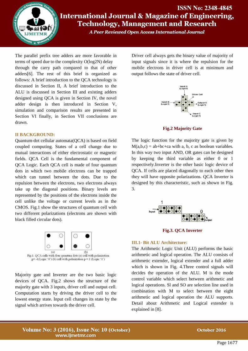
Majority gate and Inverter are the two basic logic
devices of QCA. Fig.2 shows the structure of the
majority gate with 3 inputs, driver cell and output cell.
Computation starts by driving the driver cell to the
lowest energy state. Input cell changes its state by the
signal which arrives towards the driver cell.
Driver cell always gets the binary value of majority of
input signals since it is where the repulsion for the
mobile electrons in driver cell is at minimum and
output follows the state of driver cell.
Fig.2 Majority Gate
The logic function for the majority gate is given by
M(a,b,c) = ab+bc+ca with a, b, c as boolean variables.
In this way two input AND, OR gates can be designed
by keeping the third variable as either 0 or 1
respectively.Inverter is the other basic logic device of
QCA. If cells are placed diagonally to each other then
they will have opposite polarizations. QCA Inverter is
designed by this characteristic, such as shown in Fig.
3.
Fig.3. QCA Inverter
III.1- Bit ALU Architecture:
The Arithmetic Logic Unit (ALU) performs the basic
arithmetic and logical operation. The ALU consists of
arithmetic extender, logical extender and a full adder
which is shown in Fig. 4.Three control signals will
decides the operation of the ALU. M is the mode
control variable which select between arithmetic and
logical operations. Sl and SO are selection line used in
combination with M to select between the eight
arithmetic and logical operation the ALU supports.
Detail about Arithmetic and Logical extender is
explained in [8].

Page 1678
Fig .4: Architecture of ALU
Three control signals determine the operation of the
ALU. M is the mode control variable used to select
between arithmetic and logical operations. S1 and S0
are used in combination with M to select between the
eight arithmetic and logical operation the ALU
supports.
A. Arithmetic Extender
The Arithmetic extender modifies the second operand
and passes it to the Full adder to the arithmetic as
shown in Table I and Table II.
According to truth table we write Boolean equation of
arithmetic extender shown in equation (1) and design
logic circuit of arithmetic extender shown in fig. 5.
Fig 5: Logic Circuit of Arithmetic Extender
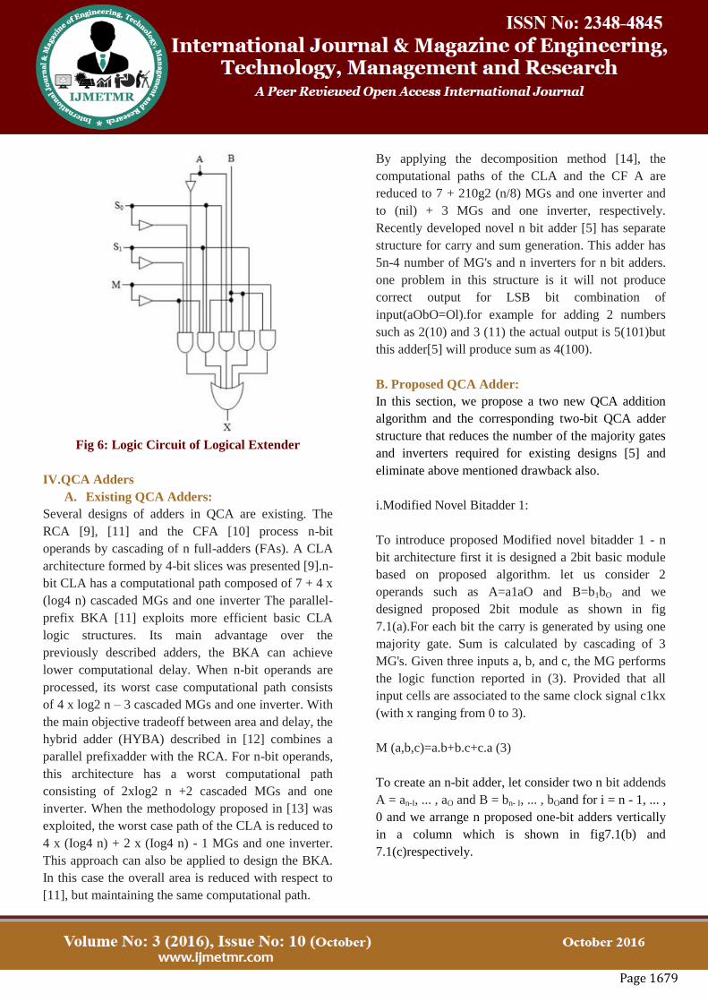
B. Logical Extender
The logic operations are performed in the logic
extender as evident from Table III and Table IV. The
FAs are used simply as connection for the outputs.
According to truth table we write Boolean equation of
logical extender shown in equation (2) and design
logic circuit of logical extender shown in fig. 6.
Page 1679
Fig 6: Logic Circuit of Logical Extender
IV.QCA Adders
A. Existing QCA Adders:
Several designs of adders in QCA are existing. The
RCA [9], [11] and the CFA [10] process n-bit
operands by cascading of n full-adders (FAs). A CLA
architecture formed by 4-bit slices was presented [9].n-
bit CLA has a computational path composed of 7 + 4 x
(log4 n) cascaded MGs and one inverter The parallel-
prefix BKA [11] exploits more efficient basic CLA
logic structures. Its main advantage over the
previously described adders, the BKA can achieve
lower computational delay. When n-bit operands are
processed, its worst case computational path consists
of 4 x log2 n – 3 cascaded MGs and one inverter. With
the main objective tradeoff between area and delay, the
hybrid adder (HYBA) described in [12] combines a
parallel prefixadder with the RCA. For n-bit operands,
this architecture has a worst computational path
consisting of 2xlog2 n +2 cascaded MGs and one
inverter. When the methodology proposed in [13] was
exploited, the worst case path of the CLA is reduced to
4 x (Iog4 n) + 2 x (Iog4 n) - 1 MGs and one inverter.
This approach can also be applied to design the BKA.
In this case the overall area is reduced with respect to
[11], but maintaining the same computational path.
By applying the decomposition method [14], the
computational paths of the CLA and the CF A are
reduced to 7 + 210g2 (n/8) MGs and one inverter and
to (nil) + 3 MGs and one inverter, respectively.
Recently developed novel n bit adder [5] has separate
structure for carry and sum generation. This adder has
5n-4 number of MG's and n inverters for n bit adders.
one problem in this structure is it will not produce
correct output for LSB bit combination of
input(aObO=Ol).for example for adding 2 numbers
such as 2(10) and 3 (11) the actual output is 5(101)but
this adder[5] will produce sum as 4(100).
B. Proposed QCA Adder:
In this section, we propose a two new QCA addition
algorithm and the corresponding two-bit QCA adder
structure that reduces the number of the majority gates
and inverters required for existing designs [5] and
eliminate above mentioned drawback also.
i.Modified Novel Bitadder 1:
To introduce proposed Modified novel bitadder 1 - n
bit architecture first it is designed a 2bit basic module
based on proposed algorithm. let us consider 2
operands such as A=a1aO and B=b1bO and we
designed proposed 2bit module as shown in fig
7.1(a).For each bit the carry is generated by using one
majority gate. Sum is calculated by cascading of 3
MG's. Given three inputs a, b, and c, the MG performs
the logic function reported in (3). Provided that all
input cells are associated to the same clock signal c1kx
(with x ranging from 0 to 3).
M (a,b,c)=a.b+b.c+c.a (3)
To create an n-bit adder, let consider two n bit addends
A = an-I, ... , aO and B = bn- I, ... , bOand for i = n - 1, ... ,
0 and we arrange n proposed one-bit adders vertically
in a column which is shown in fig7.1(b) and
7.1(c)respectively.

Page 1680
Fig 7.1(a): Modified novel bit adder 1: 2 bit basic
module.
Fig 7.1(b): Modified novel bit adder 1-Calculation
of xO
This proposed architecture can be implemented by
using equation (4) and (5)
Ci+1= M (ai,bi,ci )
(4)
Si=M (M (M (ai, bi, di-1), M (ai,bi,ci), di), di, Ci) (5)
Where di=~ci+1
Fig 7.1(c): Modified novel bit adder I: n bit basic
module
The proposed n bit QCA adder consists of 4n+ 1
number of majority gates and n+2 inverters. It results
in reduced hardware compared to the existing [5]
structure and retains the simple clocking scheme.
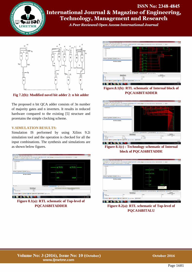
ii.Modified Novel Bit Adder 2:
Here we now introduce a new Modified novel bit
adder 2- n bit adder architecture which reduces
hardware complexity compared to existing[5] and
Modified novel bit adder 1 structure. The basic 2bit
module for Modified novel bit adder 2 is shown in fig
7.2(a).Here the carry is calculated in same way as in
proposed 1 structure and sum block is modified which
requires two majority gates only.
This proposed architecture can be implemented by
using equation (6) and (7)
Ci+1= M (ai,bi,ci )
(6)
Si=M(M (ai, bi, di-1), di, Ci)
(7)
Where di=~ci+1
To create an n-bit adder, let consider two nbit addends
A = an- I, ... , aO and B = bn- I, ... , bOand for i = n - 1, ... ,
0 and we arrange n proposed one-bit adders vertically
in a column which is shown in fig 7.2(b).
Fig 7.2(a): Modified novel bitadder 2: 2bit basic
module
Page 1681
Fig 7.2(b): Modified novel bit adder 2: n bit adder
The proposed n bit QCA adder consists of 3n number
of majority gates and n inverters. It results in reduced
hardware compared to the existing [5] structure and
proretains the simple clocking scheme.
V.SIMULATION RESULTS:
Simulation IS performed by using Xilinx 9.2i
simulation tool and the operation is checked for all the
input combinations. The synthesis and simulations are
as shown below figures.
Figure 8.1(a): RTL schematic of Top-level of
PQCA16BITADDER
Figure.8.1(b): RTL schematic of Internal block of
PQCA16BITADDER
Figure 8.1(c) : Technology schematic of Internal
block of PQCA16BITADDE
Figure 8.2(a): RTL schematic of Top-level of
PQCA16BITALU
Page 1682
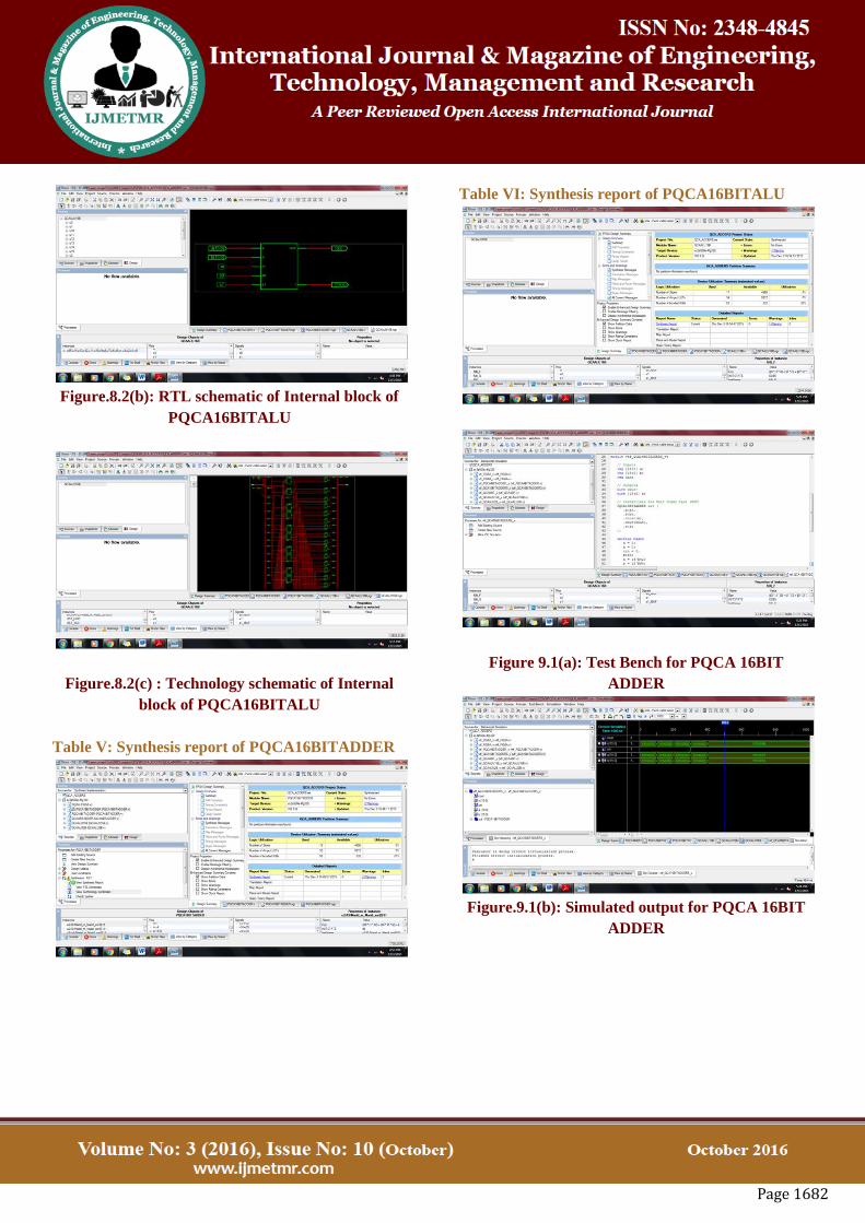
Figure.8.2(b): RTL schematic of Internal block of
PQCA16BITALU
Figure.8.2(c) : Technology schematic of Internal
block of PQCA16BITALU
Table V: Synthesis report of PQCA16BITADDER
Table VI: Synthesis report of PQCA16BITALU
Figure 9.1(a): Test Bench for PQCA 16BIT
ADDER
Figure.9.1(b): Simulated output for PQCA 16BIT
ADDER

Page 1683
Figure.9.2(a): Test Bench for PQCA 16BIT ALU
Figure.9.2(b): Simulated output for PQCA 16BIT
ALU
CONCLUSION:
A simple approach is proposed in this paper to reduce
the area and power of adder architecture. The logic
operations eliminated all the redundant logic
operations of the conventional adder and proposed a
new logic formulation for the adder. A new adder in
QCA technology was designed which achieves
reduced area than all the existing QCA adders [5]. The
Proposed modified novel bit adder 2 is implemented in
I bit ALU circuit to improve the efficiency. The
proposed ALU has total gate count of 54 which is
reduced than existing ALU [8] in which gate count is
66.The delay required for proposed ALU structure is
11.904ns which is less than existing in which 15.433ns
is needed. The functionality is checked by using Xilinx
ISE 9.2i simulation tool The Future extension of our
work is to design 16 bit ALU in QCA using Modified
novel bit adder 2 structure.
FUTURE SCOPE:
The proposed work can be extended to design of area
efficient and high speed Multiplier and Accumulators
(MAC) and digital code converters
REFERENCES:
[1]C. S. Lent, P. D. Tougaw, W. Porod, and G. H.
Bernestein, "Quantum cellular automata,"
Nanotechnology, vol. 4, no. I, pp. 49-57, 1993.
[2]The National Technology Roadmap for
Semiconductors. Semiconductor Industry
Association,1997.
[3]M. T. Niemer and P. M. Kogge, "Problems in
designing with QCAs: Layout = Timing," Int. J.
Circuit Theory Appl., vol. 29, no. I, pp. 49--62, 2001.
[4]K. Walus, G. A. Jullien, and V. S. Dimitrov,
"Computer arithmetic structures for quantum cellular
automata," in Proc. Asilomar Conf. Sygnals, Syst.
Comput., Nov. 2003, pp. 1435- 1439.
[5]StefaniaPerri, Pasquale Corsonello, and Giuseppe
Cocorullo" Area Delay Efficient Binary Adders in
QCA"IEEE transactions on very large scale integration
(vlsi) systems, vol. 22, no. 5, may 2014.
[6]RajithaChandragiri, 2, P. VenkataLavanya
International Journal of Computational Engineering
Research Vol,03Issue, 8 Design and Testing Of Prefix
Adder for High Speed Application by Using Veri log
HDL.
[7]P.D. Tougaw and C.S. Lent. Logical devices
implemented using quantum cellular automata. Journal
of Applied Physics, 75:1818, 1994.
[8]Namit Gupta, K.K. Choudhary and SumantKatiyal
"One Bit Arithmetic Logic Unit (ALU) in QCA" Int. J.
on Recent Trends in Engineering and Technology,
Vol. 8, No. 2, Jan 2013.
Page 1684
[9]H. Cho and E. E. Swartzlander, "Adder design and
analyses for quantum-dot cellular automata," IEEE
Trans. Nanotechnol., vol. 6, no. 3,pp. 374-383, May
2007.
[10]I-I. Cho and E. E. Swartzlander, "Adder and
multiplier design in quantum-dot cellular automata,"
IEEE Trans. Comput., vol. 58, no. 6, pp. 721-727, Jun.
2009.
Bibliography:
Suroj sharath Chandra
Has completed his B.Tech in Electronics and
Communication Engineering. He is pursuing M.Tech
in VLSI & ES from Siddhartha College of Engineering
and Technology, Hyderabad,
Dr. S.Vamshi Krishna
Is a proficient Ph.D person in the research area of
embedded systems from VBS Poorvanchal University,
along with initial degrees of Bachelor of Technology
in Electronics and Communication Engineering (ECE)
from JNTU Hyderabad and Master of Technology in
Electronics and Communication Engineering (ECE)
Poorvanchal University. He has 13 years of teaching
experience and has published 10 Papers in
International Journals, 2 Papers in National Journals
and has been noted under 4 International Conferences.
He has a fellowship of The Institution of Electronics
and Telecommunication Engineers (IETE) along with
a Life time membership of Indian Society for
Technical Education (ISTE). He is currently bounded
as a Professor in ECE department and is being chaired
as Director at Siddhartha Institute of Engineering and
Technology, Ibrahimpatnam, Hyderabad.
Dr. D Subba Rao
Is a proficient Ph.D person in the research area of
Image Processing from Vel-Tech University, Chennai
along with initial degrees of Bachelor of Technology
in Electronics and Communication Engineering (ECE)
from Dr. S G I E T, Markapur and Master of
Technology in Embedded Systems from SRM
University, Chennai. He has 13 years of teaching
experience and has published 12 Papers in
International Journals, 2 Papers in National Journals
and has been noted under 4 International Conferences.
He has a fellowship of The Institution of Electronics
and Telecommunication Engineers (IETE) along with
a Life time membership of Indian Society for
Technical Education (ISTE). He is currently bounded
as an Associate Professor and is being chaired as Head
of the Department for Electronics and Communication
Engineering discipline at Siddhartha Institute of
Engineering and Technology, Ibrahimpatnam,
Hyderabad.