programmable timing control hub™ for p4 ™ processor
TRANSCRIPT
IntegratedCircuitSystems, Inc.
ICS951402Advance Information
0660—05/05/05
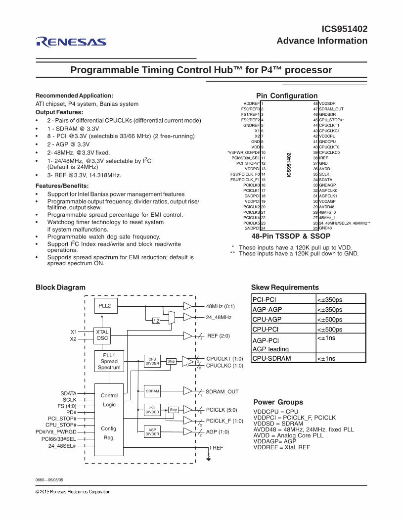
Block Diagram
Pin ConfigurationRecommended Application:ATI chipset, P4 system, Banias systemOutput Features:• 2 - Pairs of differential CPUCLKs (differential current mode)• 1 - SDRAM @ 3.3V• 8 - PCI @3.3V (selectable 33/66 MHz) (2 free-running)• 2 - AGP @ 3.3V• 2- 48MHz, @3.3V fixed.• 1- 24/48MHz, @3.3V selectable by I2C
(Default is 24MHz)• 3- REF @3.3V, 14.318MHz.
Features/Benefits:• Support for Intel Banias power management features• Programmable output frequency, divider ratios, output rise/
falltime, output skew.• Programmable spread percentage for EMI control.• Watchdog timer technology to reset system
if system malfunctions.• Programmable watch dog safe frequency.• Support I2C Index read/write and block read/write
operations.• Supports spread spectrum for EMI reduction; default is
spread spectrum ON.
Programmable Timing Control Hub™ for P4™ processor
* These inputs have a 120K pull up to VDD.** These inputs have a 120K pull down to GND.
48-Pin TSSOP & SSOP
Power GroupsVDDCPU = CPUVDDPCI = PCICLK_F, PCICLKVDDSD = SDRAMAVDD48 = 48MHz, 24MHz, fixed PLLAVDD = Analog Core PLLVDDAGP= AGPVDDREF = Xtal, REF
Skew Requirements
VDDREF 1 48 VDDSDRFS0/REF0 2 47 SDRAM_OUTFS1/REF1 3 46 GNDSDRFS2/REF2 4 45 CPU_STOP#*GNDREF 5 44 CPUCLKT1
X1 6 43 CPUCLKC1X2 7 42 VDDCPU
GND 8 41 GNDCPUVDD 9 40 CPUCLKT0
*VttPWR_GD/PD# 10 39 CPUCLKC0PCI66/33#_SEL 11 38 IREF
PCI_STOP#* 12 37 GNDVDDPCI 13 36 AVDD
FS3/PCICLK_F0 14 35 SCLKFS4/PCICLK_F1 15 34 SDATA
PCICLK0 16 33 GNDAGPPCICLK1 17 32 AGPCLK0GNDPCI 18 31 AGPCLK1VDDPCI 19 30 VDDAGP
PCICLK2 20 29 AVDD48PCICLK3 21 28 48MHz_0PCICLK4 22 27 48MHz_1PCICLK5 23 26 24_48MHz/SEL24_48#MHz**GNDPCI 24 25 GND48
ICS
9514
02
PCI-PCI <±350ps
AGP-AGP <±350ps
CPU-AGP <±500ps
CPU-PCI <±500ps
CPU-SDRAM <±1ns
AGP-PCI AGP leading
<±1ns
I REF
CPUDIVDER
PLL2
PLL1Spread
Spectrum
48MHz (0:1)
24_48MHz
PCICLK (5:0)
AGP (1:0)
PCICLK_F (1:0)
2
2
1
6
3
X1X2
XTALOSC
SDRAM SDRAM_OUT
PCIDIVDER
Stop
SDATASCLK
FS (4:0)PD#
PCI_STOP#CPU_STOP#
PD#/Vtt_PWRGDPCI66/33#SEL
24_48SEL#
Control
Logic
Config.
Reg.
/ 2
REF (2:0)
AGPDIVDER
Stop
2
2 CPUCLKT (1:0)CPUCLKC (1:0)

2
IntegratedCircuitSystems, Inc.
ICS951402Advance Information
0660—05/05/05
Pin DescriptionPIN NUMBER PIN NAME TYPE DESCRIPTION
1 VDDREF PWR Ref, XTAL power supply, nominal 3.3V2 FS0/REF0 I/O Frequency select latch input pin / 14.318 MHz reference clock.3 FS1/REF1 I/O Frequency select latch input pin / 14.318 MHz reference clock.4 FS2/REF2 I/O Frequency select latch input pin / 14.318 MHz reference clock.5 GNDREF PWR Ground pin for the REF outputs.6 X1 IN Crystal input, Nominally 14.318MHz. 7 X2 OUT Crystal output, Nominally 14.318MHz8 GND PWR Ground pin.9 VDD PWR Power supply, nominal 3.3V
10 *VttPWR_GD/PD# IN
This 3.3V LVTTL input is a level sensitive strobe used to determine when latch inputs are valid and are ready to be sampled. This is an active high input. / Asynchronous active low input pin used to power down the device into a low power state.
11 PCI66/33#_SEL INSelects all PCI clock frequencies to be 33Mhz or 66Mhz. 0 = 33Mhz , 1 = 66Mhz
12 PCI_STOP#* INStops all PCICLKs besides the PCICLK_F clocks at logic 0 level, when input low
13 VDDPCI PWR Power supply for PCI clocks, nominal 3.3V14 FS3/PCICLK_F0 I/O Frequency select latch input pin / 3.3V PCI free running clock output.15 FS4/PCICLK_F1 I/O Frequency select latch input pin / 3.3V PCI free running clock output.16 PCICLK0 OUT PCI clock output. 17 PCICLK1 OUT PCI clock output. 18 GNDPCI PWR Ground pin for the PCI outputs19 VDDPCI PWR Power supply for PCI clocks, nominal 3.3V20 PCICLK2 OUT PCI clock output. 21 PCICLK3 OUT PCI clock output. 22 PCICLK4 OUT PCI clock output. 23 PCICLK5 OUT PCI clock output. 24 GNDPCI PWR Ground pin for the PCI outputs25 GND48 PWR Ground pin for the 48MHz outputs
26 24_48MHz/SEL24_48#MHz** I/O24/48MHz clock output / Latched select input for 24/48MHz output. 0=48MHz, 1 = 24MHz.
27 48MHz_1 OUT 48MHz clock output.28 48MHz_0 OUT 48MHz clock output.29 AVDD48 PWR Analog power for 48MHz outputs and fixed PLL core, nominal 3.3V30 VDDAGP PWR Power supply for AGP clocks, nominal 3.3V31 AGPCLK1 OUT AGP clock output32 AGPCLK0 OUT AGP clock output33 GNDAGP PWR Ground pin for the AGP outputs34 SDATA I/O Data pin for SMBus circuitry, 5V tolerant. 35 SCLK IN Clock pin of SMBus circuitry, 5V tolerant. 36 AVDD PWR 3.3V Analog Power pin for Core PLL37 GND PWR Ground pin.
38 IREF OUT
This pin establishes the reference current for the differential current-mode output pairs. This pin requires a fixed precision resistor tied to ground in order to establish the appropriate current. 475 ohms is the standard value.
39 CPUCLKC0 OUTComplementary clock of differential pair CPU outputs. This clock is 180 degrees out of phase with the SDRAM clock.
40 CPUCLKT0 OUTTrue clock of differential pair CPU outputs. This clock is in phase with the SDRAM clock
41 GNDCPU PWR Ground pin for the CPU outputs42 VDDCPU PWR Supply for CPU clocks, 3.3V nominal
43 CPUCLKC1 OUTComplementary clock of differential pair CPU outputs. This clock is 180 degrees out of phase with the SDRAM clock.
44 CPUCLKT1 OUTTrue clock of differential pair CPU outputs. This clock is in phase with the SDRAM clock
45 CPU_STOP#* IN Stops all CPUCLK besides the free running clocks46 GNDSDR PWR Ground pin for the SDRAM outputs.47 SDRAM_OUT OUT SDRAM seed clock output for external buffer48 VDDSDR PWR Supply for SDRAM clocks, nominal 3.3V.

3
IntegratedCircuitSystems, Inc.
ICS951402Advance Information
0660—05/05/05
Table 1: Clock Power Management Truth Table Byte 6 Bit 6
Byte 6 Bit 7
PD# CPU_ STOP
Stoppable CPU
(Not free-run)
Non-stop CPU
(Free-run) Note
0 0 0 0 IREF x 2 IREF x 2 0 0 0 1 IREF x 2 IREF x 2 0 0 1 0 IREF x 6 RUN0 0 1 1 RUN RUN
Non Tri-state
Mode
0 1 0 0 Hi Z IREF x 20 1 0 1 Hi Z IREF x 2 0 1 1 0 Hi Z RUN0 1 1 1 RUN RUN
CPU_stop# Tri-state
Mode
1 0 0 0 Hi Z Hi Z1 0 0 1 Hi Z Hi Z1 0 1 0 IREFx6 RUN1 0 1 1 RUN RUN
PD# & Tri-state
Mode
1 1 0 0 Hi Z Hi Z1 1 0 1 Hi Z Hi Z 1 1 1 0 HI Z RUN 1 1 1 1 RUN RUN
PD# & CPU_stop#
Tri-state Mode

4
IntegratedCircuitSystems, Inc.
ICS951402Advance Information
0660—05/05/05*See notes on the following page.
General I2C serial interface information for the ICS951402
How to Write:• Controller (host) sends a start bit.• Controller (host) sends the write address D2 (H)
• ICS clock will acknowledge• Controller (host) sends the begining byte location = N• ICS clock will acknowledge• Controller (host) sends the data byte count = X• ICS clock will acknowledge• Controller (host) starts sending Byte N through
Byte N + X -1(see Note 2)
• ICS clock will acknowledge each byte one at a time• Controller (host) sends a Stop bit
How to Read:• Controller (host) will send start bit.• Controller (host) sends the write address D2
(H)
• ICS clock will acknowledge• Controller (host) sends the begining byte
location = N• ICS clock will acknowledge• Controller (host) will send a separate start bit.• Controller (host) sends the read address D3 (H)
• ICS clock will acknowledge• ICS clock will send the data byte count = X• ICS clock sends Byte N + X -1• ICS clock sends Byte 0 through byte X (if X(H)
was written to byte 8).• Controller (host) will need to acknowledge each
byte• Controllor (host) will send a not acknowledge bit• Controller (host) will send a stop bit
ICS (Slave/Receiver)T
WRACK
ACK
ACK
ACK
ACKP stoP bit
X By
te
Index Block Write Operation
Slave Address D2(H)
Beginning Byte = N
WRite
starT bitController (Host)
Byte N + X - 1
Data Byte Count = X
Beginning Byte N
T starT bit
WR WRite
RT Repeat starT
RD ReaD
Beginning Byte N
Byte N + X - 1N Not acknowledgeP stoP bit
Slave Address D3(H)
Index Block Read Operation
Slave Address D2(H)
Beginning Byte = NACK
ACK
Data Byte Count = X
ACK
ICS (Slave/Receiver)Controller (Host)
X By
te
ACK
ACK
5
IntegratedCircuitSystems, Inc.
ICS951402Advance Information
0660—05/05/05
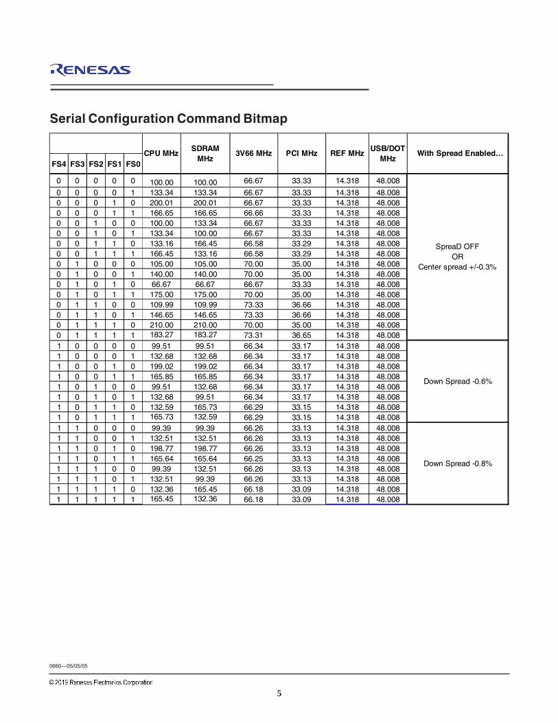
Serial Configuration Command Bitmap
FS4 FS3 FS2 FS1 FS0
0 0 0 0 0 100.00 100.00 66.67 33.33 14.318 48.008
0 0 0 0 1 133.34 133.34 66.67 33.33 14.318 48.0080 0 0 1 0 200.01 200.01 66.67 33.33 14.318 48.0080 0 0 1 1 166.65 166.65 66.66 33.33 14.318 48.0080 0 1 0 0 100.00 133.34 66.67 33.33 14.318 48.0080 0 1 0 1 133.34 100.00 66.67 33.33 14.318 48.0080 0 1 1 0 133.16 166.45 66.58 33.29 14.318 48.0080 0 1 1 1 166.45 133.16 66.58 33.29 14.318 48.0080 1 0 0 0 105.00 105.00 70.00 35.00 14.318 48.0080 1 0 0 1 140.00 140.00 70.00 35.00 14.318 48.0080 1 0 1 0 66.67 66.67 66.67 33.33 14.318 48.0080 1 0 1 1 175.00 175.00 70.00 35.00 14.318 48.0080 1 1 0 0 109.99 109.99 73.33 36.66 14.318 48.0080 1 1 0 1 146.65 146.65 73.33 36.66 14.318 48.0080 1 1 1 0 210.00 210.00 70.00 35.00 14.318 48.0080 1 1 1 1 183.27 183.27 73.31 36.65 14.318 48.0081 0 0 0 0 99.51 99.51 66.34 33.17 14.318 48.0081 0 0 0 1 132.68 132.68 66.34 33.17 14.318 48.0081 0 0 1 0 199.02 199.02 66.34 33.17 14.318 48.0081 0 0 1 1 165.85 165.85 66.34 33.17 14.318 48.0081 0 1 0 0 99.51 132.68 66.34 33.17 14.318 48.0081 0 1 0 1 132.68 99.51 66.34 33.17 14.318 48.0081 0 1 1 0 132.59 165.73 66.29 33.15 14.318 48.0081 0 1 1 1 165.73 132.59 66.29 33.15 14.318 48.0081 1 0 0 0 99.39 99.39 66.26 33.13 14.318 48.0081 1 0 0 1 132.51 132.51 66.26 33.13 14.318 48.0081 1 0 1 0 198.77 198.77 66.26 33.13 14.318 48.0081 1 0 1 1 165.64 165.64 66.25 33.13 14.318 48.0081 1 1 0 0 99.39 132.51 66.26 33.13 14.318 48.0081 1 1 0 1 132.51 99.39 66.26 33.13 14.318 48.0081 1 1 1 0 132.36 165.45 66.18 33.09 14.318 48.0081 1 1 1 1 165.45 132.36 66.18 33.09 14.318 48.008
3V66 MHz PCI MHzSDRAM
MHz
Down Spread -0.8%
SpreaD OFFOR
Center spread +/-0.3%
Down Spread -0.6%
CPU MHz REF MHzUSB/DOT
MHzWith Spread Enabled…

6
IntegratedCircuitSystems, Inc.
ICS951402Advance Information
0660—05/05/05
I2C Table: Reserved Register
Byte 0 Pin # Name Control Function
Type 0 1 PWD
Bit 7 - Reserved Reserved RW - - 1 Bit 6 - Reserved Reserved RW - - 1 Bit 5 - Reserved Reserved RW - - 1 Bit 4 - Reserved Reserved RW - - 1 Bit 3 - Reserved Reserved RW - - 1 Bit 2 - Reserved Reserved RW - - 1 Bit 1 - Reserved Reserved RW - - 1 Bit 0 - Reserved Reserved RW - - 1
I2C Table: Reserved Register
Byte 1 Pin # Name Control Function
Type 0 1 PWD
Bit 7 - Reserved Reserved RW - - 1 Bit 6 - Reserved Reserved RW - - 1 Bit 5 - Reserved Reserved RW - - 1 Bit 4 - Reserved Reserved RW - - 1 Bit 3 - Reserved Reserved RW - - 1 Bit 2 - Reserved Reserved RW - - 1 Bit 1 - Reserved Reserved RW - - 1 Bit 0 - Reserved Reserved RW - - 1
I2C Table: Reserved Register
Byte 2 Pin # Name Control Function
Type 0 1 PWD
Bit 7 - Reserved Reserved RW - - 1 Bit 6 - Reserved Reserved RW - - 1 Bit 5 - Reserved Reserved RW - - 1 Bit 4 - Reserved Reserved RW - - 1 Bit 3 - Reserved Reserved RW - - 1 Bit 2 - Reserved Reserved RW - - 1 Bit 1 - Reserved Reserved RW - - 1 Bit 0 - Reserved Reserved RW - - 1

7
IntegratedCircuitSystems, Inc.
ICS951402Advance Information
0660—05/05/05
I2C Table: Reserved Register
Byte 3 Pin # Name Control Function
Type 0 1 PWD
Bit 7 - Reserved Reserved RW - - 1 Bit 6 - Reserved Reserved RW - - 1 Bit 5 - Reserved Reserved RW - - 1 Bit 4 - Reserved Reserved RW - - 1 Bit 3 - Reserved Reserved RW - - 1 Bit 2 - Reserved Reserved RW - - 1 Bit 1 - Reserved Reserved RW - - 1 Bit 0 - Reserved Reserved RW - - 1
I2C Table: Functionality and Frequency Select Register
Byte 4 Pin # Name Control Function Type 0 1 PWD
Bit 7 - FS3 Freq Select Bit 7 RW 0 Bit 6 - FS2 Freq Select Bit 6 RW 0 Bit 5 - FS1 Freq Select Bit 5 RW 0 Bit 4 - FS0 Freq Select Bit 4 RW
See
Frequency Table
0
Bit 3 - FS Source Frequency H/W or IIC Select RW Latch Input IIC 0
Bit 2 - FS4 Freq Select Bit 2 RW See Frequency Table 0 Bit 1 - SS_EN SPREAD Enable RW OFF ON 1 Bit 0 - All Outputs Output Control RW Normal Tri-state 0
Note: If Byte4 bit1 = 0 then FS4=0 I2C Table: Output Control and Read Back Register
Byte 5 Pin # Name Control Function Type 0 1 PWD
Bit 7 31 AGP1 Output Control RW Disable Enable 1 Bit 6 32 AGP0 Output Control RW Disable Enable 1 Bit 5 26 24_48#SEL 24 or 48 Select RW 48MHz 24MHz X Bit 4 - FS4RB FS4 Read back R - - X Bit 3 - FS3RB FS3 Read back R - - X Bit 2 - FS2RB FS2 Read back R - - X Bit 1 - FS1RB FS1 Read back R - - X Bit 0 - FS0RB FS0 Read back R - - X
8
IntegratedCircuitSystems, Inc.
ICS951402Advance Information
0660—05/05/05
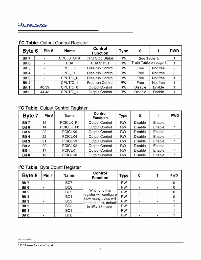
I2C Table: Output Control Register
Byte 6 Pin # Name Control Function
Type 0 1 PWD
Bit 7 - CPU_STOP# CPU Stop Status RW 1 Bit 6 - PD# PD# Status RW
See Table 1: Truth Table on page 3 1
Bit 5 - PCI_F0 Free-run Control RW Free Not free 0 Bit 4 - PCI_F1 Free-run Control RW Free Not free 0 Bit 3 - CPUT/C_0 Free-run Control RW Free Not free 1 Bit 2 - CPUT/C_1 Free-run Control RW Free Not free 1 Bit 1 40,39 CPUT/C_0 Output Control RW Disable Enable 1 Bit 0 44,43 CPUT/C_1 Output Control RW Disable Enable 1
I2C Table: Output Control Register
Byte 7 Pin # Name Control Function
Type 0 1 PWD
Bit 7 15 PCICLK_F1 Output Control RW Disable Enable 1 Bit 6 14 PCICLK_F0 Output Control RW Disable Enable 1 Bit 5 23 PCICLK5 Output Control RW Disable Enable 1 Bit 4 22 PCICLK4 Output Control RW Disable Enable 1 Bit 3 21 PCICLK3 Output Control RW Disable Enable 1 Bit 2 20 PCICLK2 Output Control RW Disable Enable 1 Bit 1 17 PCICLK1 Output Control RW Disable Enable 1 Bit 0 16 PCICLK0 Output Control RW Disable Enable 1
I2C Table: Byte Count Register
Byte 8 Pin # Name Control Function
Type 0 1 PWD
Bit 7 - BC7 RW - - 0 Bit 6 - BC6 RW - - 0 Bit 5 - BC5 RW - - 0 Bit 4 - BC4 RW - - 0 Bit 3 - BC3 RW - - 1 Bit 2 - BC2 RW - - 1 Bit 1 - BC1 RW - - 1 Bit 0 - BC0
Writing to this register will configure how many bytes will be read back, default
is 0F = 15 bytes.
RW - - 1

9
IntegratedCircuitSystems, Inc.
ICS951402Advance Information
0660—05/05/05
I2C Table: Watchdog Timer Register
Byte 9 Pin # Name Control Function Type 0 1 PWD
Bit 7 - WD7 RW - - 0 Bit 6 - WD6 RW - - 0 Bit 5 - WD5 RW - - 0 Bit 4 - WD4 RW - - 1 Bit 3 - WD3 RW - - 0 Bit 2 - WD2 RW - - 0 Bit 1 - WD1 RW - - 0 Bit 0 - WD0
These bits represent X*293ms the
watchdog timer will wait before it goes to alarm mode. Default is 16 X 293ms =4.688
seconds RW - - 0
I2C Table: WD Timer Control Register
Byte 10 Pin # Name Control Function
Type 0 1 PWD
Bit 7 - M/NEN M/N Programming Enable RW
Latched Inputs
IIC Prog. B (11:17) 0
Bit 6 - WDEN Watchdog Enable RW Disable Enable 0
Bit 5 - WDStatus WD Status Control RW OFF ON 0
Bit 4 - WD SF4 RW - - 1 Bit 3 - WD SF3 RW - - 0 Bit 2 - WD SF2 RW - - 0 Bit 1 - WD SF1 RW - - 0 Bit 0 - WD SF0
Writing to these bit will configure the safe
frequency as Byte 0 Bit (6:0)
RW - - 0 Note: If Byte4 bit1 = 0 then FS4=0 I2C Table: VCO Frequency Control Register
Byte 11 Pin # Name Control
Function Type 0 1 PWD
Bit 7 - N Div8 N Divider Bit 8 RW - - X Bit 6 - M Div6 RW - - X Bit 5 - M Div5 RW - - X Bit 4 - M Div4 RW - - X Bit 3 - M Div3 RW - - X Bit 2 - M Div2 RW - - X Bit 1 - M Div1 RW - - X Bit 0 - M Div0
The decimal representation of M Div (6:0) is equal to
reference divider value. Default at
power up = latch-in or Byte 0 Rom table. RW - - X

10
IntegratedCircuitSystems, Inc.
ICS951402Advance Information
0660—05/05/05
I2C Table: VCO Frequency Control Register
Byte 12 Pin # Name Control Function
Type 0 1 PWD
Bit 7 - N Div7 RW - - X Bit 6 - N Div6 RW - - X Bit 5 - N Div5 RW - - X Bit 4 - N Div4 RW - - X Bit 3 - N Div3 RW - - X Bit 2 - N Div2 RW - - X Bit 1 - N Div1 RW - - X Bit 0 - N Div0
The decimal representation of N Div (8:0) is equal to VCO divider value. Default at power up = latch-in or Byte 0
Rom table. RW - - X
I2C Table: Spread Spectrum Control Register
Byte 13 Pin # Name Control Function
Type 0 1 PWD
Bit 7 - SSP7 RW - - X Bit 6 - SSP6 RW - - X Bit 5 - SSP5 RW - - X Bit 4 - SSP4 RW - - X Bit 3 - SSP3 RW - - X Bit 2 - SSP2 RW - - X Bit 1 - SSP1 RW - - X Bit 0 - SSP0
These Spread Spectrum bits will
program the spread percentage. It is
recommended to use ICS Spread % table
for spread programming.
RW - - X
I2C Table: Spread Spectrum Control Register
Byte 14 Pin # Name Control
Function Type 0 1 PWD
Bit 7 - Reserved Reserved R - - X Bit 6 - Reserved Reserved R - - X Bit 5 - Reserved Reserved R - - X Bit 4 - SSP12 RW - - X Bit 3 - SSP11 RW - - X Bit 2 - SSP10 RW - - X Bit 1 - SSP9 RW - - X Bit 0 - SSP8
It is recommended to use ICS Spread % table for spread
programming. RW - - X

11
IntegratedCircuitSystems, Inc.
ICS951402Advance Information
0660—05/05/05
I2C Table: Output Divider Control Register
Byte 15 Pin # Name Control Function
Type 0 1 PWD
Bit 7 - SD Div3 RW X Bit 6 - SD Div2 RW X Bit 5 - SD Div1 RW X Bit 4 - SD Div0
SDRAM divider ratio can be configured
via these 4 bits individually. RW
See Table 2: Divider Ratio Combination
Table X
Bit 3 - CPU Div3 RW X Bit 2 - CPU Div2 RW X Bit 1 - CPU Div1 RW X Bit 0 - CPU Div0
CPU divider ratio can be configured via
these 4 bits individually. RW
See Table 2: Divider Ratio Combination
Table X
Table 2: CPU, SDRAM, AGP and PCI66 Divider Ratio Combination Table
Divider (3:2) Bit 00 01 10 11 MSB
1 2 4 8 00 0000 2 0100 4 1000 8 1100 16 01 0001 3 0101 6 1001 12 1101 24 10 0010 5 0110 10 1010 20 1110 40 11 0011 7 0111 14 1011 28 1111 56 D
ivid
er (
1:0)
LSB Address Div Address Div Address Div Address Div
Table 3: PCI33 Divider Ratio Combination Table
Divider (3:2) Bit 00 01 10 11 MSB
1 2 4 8 00 0000 4 0100 8 1000 16 1100 32 01 0001 3 0101 6 1001 12 1101 24 10 0010 5 0110 10 1010 20 1110 40 11 0011 7 0111 14 1011 28 1111 56 D
ivid
er (
1:0)
LSB Address Div Address Div Address Div Address Div

12
IntegratedCircuitSystems, Inc.
ICS951402Advance Information
0660—05/05/05
I2C Table: Output Divider Control Register
Byte 16 Pin # Name Control Function
Type 0 1 PWD
Bit 7 - AGP Div3 RW X Bit 6 - AGP Div2 RW X Bit 5 - AGP Div1 RW X Bit 4 - AGP Div0
AGP divider ratio can be configured via
these 4 bits individually RW
See Table 2: Divider Ratio Combination
Table X
Bit 3 - Reserved Reserved RW - - X Bit 2 - Reserved Reserved RW - - X Bit 1 - Reserved Reserved RW - - X Bit 0 - Reserved Reserved RW - - X
I2C Table: Output Divider Control Register
Byte 17 Pin # Name Control Function
Type 0 1 PWD
Bit 7 - AGPINV AGP Phase Invert RW Default Inverse X Bit 6 - Reserved Reserved RW - - X
Bit 5 - SDINV SDRAM Phase Invert RW Default Inverse X
Bit 4 - CPUINV CPU Phase Invert RW Default Inverse X Bit 3 - PCIDiv3 RW X Bit 2 - PCIDiv3 RW X Bit 1 - PCIDiv3 RW X Bit 0 - PCIDiv3
PCI divider ratio can be configured via
these 4 bits individually RW
See Table 2 & 3: Divider Ratio
Combination Table X
I2C Table: Group Skew Control Register
Byte 18 Pin # Name Control Function
Type 0 1 PWD
Bit 7 - CPUSkw3 RW 1 Bit 6 - CPUSkw2
CPUT Skew Control RW
See 2-bit Skew Control at table 4 0
Bit 5 - SDSkw3 RW 0 Bit 4 - SDSkw2
SDRAM Skew Control RW
See 2-bit Skew Control at table 4 1
Bit 3 - Reserved Reserved RW - - 1 Bit 2 - Reserved Reserved RW - - 1 Bit 1 - Reserved Reserved RW - - 1 Bit 0 - Reserved Reserved RW - - 1

13
IntegratedCircuitSystems, Inc.
ICS951402Advance Information
0660—05/05/05
Table 4:Skew Specification on Output Mode
Bit3 Bit2 Bit1 Bit0 Skew in ps
0 0 X X 500 0 1 X X 750 1 0 X X 1000 1 1 X X 1250
I2C Table: Group Skew Control Register
Byte 19 Pin # Name Control Function
Type 0 1 PWD
Bit 7 - Reserved Reserved RW - - 0 Bit 6 - Reserved Reserved RW - - 0 Bit 5 - Reserved Reserved RW - - 0 Bit 4 - Reserved Reserved RW - - 0 Bit 3 - AGPSkw3 RW 0 Bit 2 - AGPSkw2
AGP Skew Control RW
See 2-bit Skew Control at table 4 0
Bit 1 - Reserved Reserved RW - - 0 Bit 0 - Reserved Reserved RW - - 0
I2C Table: Group Skew Control Register
Byte 20 Pin # Name Control Function Type 0 1 PWD
Bit 7 - PCISkw3 RW 0 Bit 6 - PCISkw2
PCI_F [1:0] Skew Control RW
See 2-bit Skew Control at table 4 0
Bit 5 - Reserved Reserved RW - - 0 Bit 4 - Reserved Reserved RW - - 0 Bit 3 - PCISkw1 RW 0 Bit 2 - PCISkw0
PCI [5:0] Skew Control RW
See 2-bit Skew Control at table 4 0
Bit 1 - Reserved Reserved RW - - 0 Bit 0 - Reserved Reserved RW - - 0

14
IntegratedCircuitSystems, Inc.
ICS951402Advance Information
0660—05/05/05
I2C Table: Slew Rate Control Register
Byte 21 Pin # Name Control Function
Type 0 1 PWD
Bit 7 - 24_48Slw1 RW - - 0 Bit 6 - 24_48Slw0
24_48 Slew Rate Control RW - - 0
Bit 5 - AGPSlw1 RW - - 0 Bit 4 - AGPSlw0
AGP Slew Rate Control RW - - 0
Bit 3 - Reserved Reserved RW - - 0 Bit 2 - Reserved Reserved RW - - 0 Bit 1 - REFSlw1 RW - - 0 Bit 0 - REFSlw0
REF Slew Rate Control RW - - 0
I2C Table: Slew Rate Control Register
Byte 22 Pin # Name Control
Function Type 0 1 PWD
Bit 7 - SDSlw1 RW - - 0 Bit 6 - SDSlw0
SDRAM Slew Rate Control RW - - 0
Bit 5 - Reserved Reserved RW - - 0 Bit 4 - Reserved Reserved RW - - 0 Bit 3 - PCISlw1 RW - - 0 Bit 2 - PCISlw0
PCI_F Slew Rate Control RW - - 0
Bit 1 - PCISlw1 RW - - 0 Bit 0 - PCISlw0
PCI Slew Rate Control RW - - 0
I2C Table: Output Control Register
Byte 23 Pin # Name Control
Function Type 0 1 PWD
Bit 7 - Reserved Reserved - - - X Bit 6 27 48MHz_1 Output Control RW Disable Enable 1 Bit 5 47 SDRAM Output Control RW Disable Enable 1 Bit 4 28 48MHz_0 Output Control RW Disable Enable 1 Bit 3 26 24_48MHz Output Control RW Disable Enable 1 Bit 2 4 REF2 Output Control RW Disable Enable 1 Bit 1 3 REF1 Output Control RW Disable Enable 1 Bit 0 2 REF0 Output Control RW Disable Enable 1

15
IntegratedCircuitSystems, Inc.
ICS951402Advance Information
0660—05/05/05
I2C Table: Reserved Control Register
Byte 24 Pin # Name Control Function
Type 0 1 PWD
Bit 7 - Reserved Reserved RW - - 0 Bit 6 - Reserved Reserved RW - - 0 Bit 5 - Reserved Reserved RW - - 0 Bit 4 - Reserved Reserved RW - - 0 Bit 3 - Reserved Reserved RW - - 0 Bit 2 - Reserved Reserved RW - - 0 Bit 1 - Reserved Reserved RW - - 0 Bit 0 - Reserved Reserved RW - - 0
I2C Table: Reserved Control Register
Byte 25 Pin # Name Control Function Type 0 1 PWD
Bit 7 - Reserved Reserved RW - - 0 Bit 6 - Reserved Reserved RW - - 0 Bit 5 - Reserved Reserved RW - - 0 Bit 4 - Reserved Reserved RW - - 0 Bit 3 - Reserved Reserved RW - - 0 Bit 2 - Reserved Reserved RW - - 0 Bit 1 - Reserved Reserved RW - - 0 Bit 0 - Reserved Reserved RW - - 0

16
IntegratedCircuitSystems, Inc.
ICS951402Advance Information
0660—05/05/05
Absolute Maximum Ratings
Stresses above those listed under Absolute Maximum Ratings may cause permanent damage to the device. These ratings arestress specifications only and functional operation of the device at these or any other conditions above those listed in theoperational sections of the specifications is not implied. Exposure to absolute maximum rating conditions for extendedperiods may affect product reliability.
Core Supply Voltage . . . . . . . . . . . . . . . . . . . . . . 4.6 VI/O Supply Voltage . . . . . . . . . . . . . . . . . . . . . . . . 3.6VLogic Inputs . . . . . . . . . . . . . . . . . . . . . . . . . . . . . GND –0.5 V to VDD +0.5 VAmbient Operating Temperature . . . . . . . . . . . . 0°C to +70°CStorage Temperature . . . . . . . . . . . . . . . . . . . . . –65°C to +150°CCase Temperature . . . . . . . . . . . . . . . . . . . . . . . . 115°C
Electrical Characteristics - Input/Supply/Common Output ParametersTA = 0 - 70C; Supply Voltage VDD = 3.3 V +/-5%
PARAMETER SYMBOL CONDITIONS MIN TYP MAX UNITS
Input High Voltage VIH 2VDD
+0.3V
Input Low Voltage VILVSS -0.3
0.8 V
Input High Current IIH VIN = VDD -5 5 mA
IIL1VIN = 0 V; Inputs with no pull-up
resistors-5 mA
IIL2VIN = 0 V; Inputs with pull-up
resistors-200
Operating Supply Current IDD3.3OPCL = Full load; Select @ 100
MHz229 230 360 mA
IDD3.3OPCL =Full load; Select @ 133
MHz220 233 360 mA
Powerdown Current IDD3.3PD IREF=5 mA 38.1 45 mA
Input Frequency Fi VDD = 3.3 V 14.32 MHz
Pin Inductance Lpin 7 nH
CIN Logic Inputs 5 pF
COUT Output pin capacitance 6 pF
CINX X1 & X2 pins 27 36 45 pF
Clk Stabilization1,2 TSTABFrom PowerUp or deassertion of
PowerDown to 1st clock.1 1.8 ms
tPZH,tPZL Output enable delay (all outputs) 1 10 ns
tPHZ,tPLZ Output disable delay (all outputs) 1 10 ns
1Guaranteed by design, not 100% tested in production.2See timing diagrams for buffered and un-buffered timing requirements.
Delay1
Input Capacitance1
Input Low Current
17
IntegratedCircuitSystems, Inc.
ICS951402Advance Information
0660—05/05/05
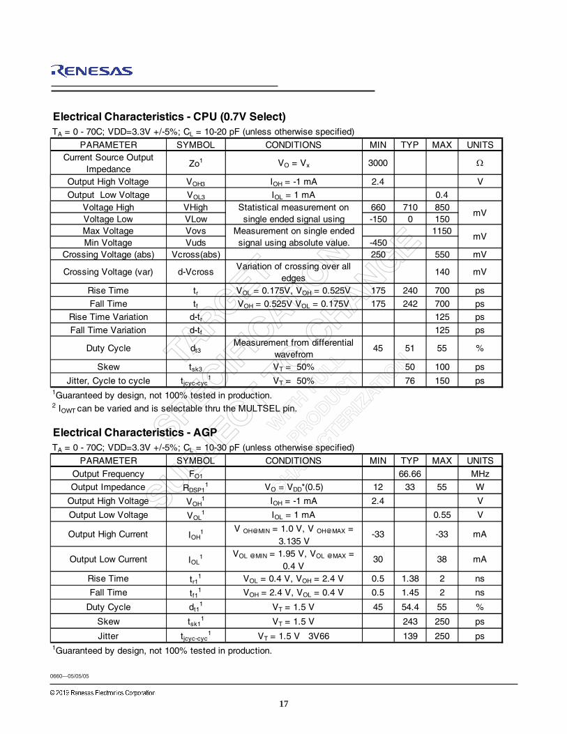
Electrical Characteristics - CPU (0.7V Select)TA = 0 - 70C; VDD=3.3V +/-5%; CL = 10-20 pF (unless otherwise specified)
PARAMETER SYMBOL CONDITIONS MIN TYP MAX UNITSCurrent Source Output
ImpedanceZo1 VO = Vx 3000 Ω
Output High Voltage VOH3 IOH = -1 mA 2.4 V
Output Low Voltage VOL3 IOL = 1 mA 0.4Voltage High VHigh 660 710 850Voltage Low VLow -150 0 150Max Voltage Vovs 1150Min Voltage Vuds -450
Crossing Voltage (abs) Vcross(abs) 250 550 mV
Crossing Voltage (var) d-VcrossVariation of crossing over all
edges140 mV
Rise Time tr VOL = 0.175V, VOH = 0.525V 175 240 700 ps
Fall Time tf VOH = 0.525V VOL = 0.175V 175 242 700 ps
Rise Time Variation d-tr 125 ps
Fall Time Variation d-tf 125 ps
Duty Cycle dt3Measurement from differential
wavefrom45 51 55 %
Skew tsk3 VT = 50% 50 100 ps
Jitter, Cycle to cycle tjcyc-cyc1 VT = 50% 76 150 ps
1Guaranteed by design, not 100% tested in production.2 IOWT
can be varied and is selectable thru the MULTSEL pin.
Statistical measurement on single ended signal using
mV
Measurement on single ended signal using absolute value.
mV
Electrical Characteristics - AGPTA = 0 - 70C; VDD=3.3V +/-5%; CL = 10-30 pF (unless otherwise specified)
PARAMETER SYMBOL CONDITIONS MIN TYP MAX UNITS
Output Frequency FO1 66.66 MHz
Output Impedance RDSP11 VO = VDD*(0.5) 12 33 55 W
Output High Voltage VOH1 IOH = -1 mA 2.4 V
Output Low Voltage VOL1 IOL = 1 mA 0.55 V
Output High Current IOH1 V OH@MIN = 1.0 V, V OH@MAX =
3.135 V-33 -33 mA
Output Low Current IOL1 VOL @MIN = 1.95 V, VOL @MAX =
0.4 V30 38 mA
Rise Time tr11 VOL = 0.4 V, VOH = 2.4 V 0.5 1.38 2 ns
Fall Time tf11 VOH = 2.4 V, VOL = 0.4 V 0.5 1.45 2 ns
Duty Cycle dt11 VT = 1.5 V 45 54.4 55 %
Skew tsk11 VT = 1.5 V 243 250 ps
Jitter tjcyc-cyc1 VT = 1.5 V 3V66 139 250 ps
1Guaranteed by design, not 100% tested in production.
18
IntegratedCircuitSystems, Inc.
ICS951402Advance Information
0660—05/05/05
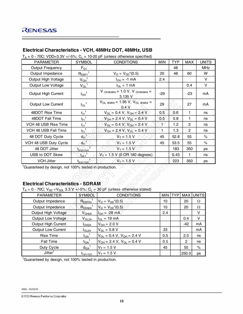
Electrical Characteristics - VCH, 48MHz DOT, 48MHz, USBTA = 0 - 70C; VDD=3.3V +/-5%; CL = 10-20 pF (unless otherwise specified)
PARAMETER SYMBOL CONDITIONS MIN TYP MAX UNITS
Output Frequency FO1 48 MHz
Output Impedance RDSP11 VO = VDD*(0.5) 20 48 60 W
Output High Voltage VOH1 IOH = -1 mA 2.4 V
Output Low Voltage VOL1 IOL = 1 mA 0.4 V
Output High Current IOH1 V OH@MIN = 1.0 V, V OH@MAX =
3.135 V-29 -23 mA
Output Low Current IOL1 VOL @MIN = 1.95 V, VOL @MAX =
0.4 V29 27 mA
48DOT Rise Time tr11 VOL = 0.4 V, VOH = 2.4 V 0.5 0.6 1 ns
48DOT Fall Time tf11 VOH = 2.4 V, VOL = 0.4 V 0.5 0.8 1 ns
VCH 48 USB Rise Time tr11 VOL = 0.4 V, VOH = 2.4 V 1 1.2 2 ns
VCH 48 USB Fall Time tf11 VOH = 2.4 V, VOL = 0.4 V 1 1.3 2 ns
48 DOT Duty Cycle dt11 VT = 1.5 V 45 52.8 55 %
VCH 48 USB Duty Cycle dt11 VT = 1.5 V 45 53.5 55 %
48 DOT Jitter tjcyc-cyc1 VT = 1.5 V 183 350 ps
USB to DOT Skew tsk11 VT = 1.5 V (0 OR 180 degrees) 0.43 1 ns
VCH Jitter tjcyc-cyc1 VT = 1.5 V 223 350 ps
1Guaranteed by design, not 100% tested in production.
Electrical Characteristics - SDRAMTA = 0 - 70C; VDD =VDDL 3.3 V +/-5%; CL = 30 pF (unless otherwise stated)
PARAMETER SYMBOL CONDITIONS MIN TYP MAX UNITS
Output Impedance RDSP2A1 VO = VDD*(0.5) 10 20 Ω
Output Impedance RDSN2A1 VO = VDD*(0.5) 10 20 Ω
Output High Voltage VOH2A IOH = -28 mA 2.4 V
Output Low Voltage VOL2A IOL = 19 mA 0.4 V
Output High Current IOH2A VOH = 2.0 V -42 mA
Output Low Current IOL2A VOL = 0.8 V 33 mA
Rise Time tr2A1 VOL = 0.4 V, VOH = 2.4 V 0.5 2.0 ns
Fall Time tf2A1 VOH = 2.4 V, VOL = 0.4 V 0.5 2 ns
Duty Cycle dt2A1 VT = 1.5 V 45 55 %
Jitter1 tcyc-cyc VT = 1.5 V 250.0 ps1Guaranteed by design, not 100% tested in production.

19
IntegratedCircuitSystems, Inc.
ICS951402Advance Information
0660—05/05/05
Electrical Characteristics - REFTA = 0 - 70C; VDD=3.3V +/-5%; CL = 10-20 pF (unless otherwise specified)
PARAMETER SYMBOL CONDITIONS MIN TYP MAX UNITS
Output Frequency FO1 MHz
Output Impedance RDSP11 VO = VDD*(0.5) 20 48 60 W
Output High Voltage VOH1 IOH = -1 mA 2.4 V
Output Low Voltage VOL1 IOL = 1 mA 0.4 V
Output High Current IOH1 V OH@MIN = 1.0 V, V OH@MAX =
3.135 V-29 -23 mA
Output Low Current IOL1 VOL @MIN = 1.95 V, VOL @MAX =
0.4 V29 27 mA
Rise Time tr11 VOL = 0.4 V, VOH = 2.4 V 1 1.25 2 ns
Fall Time tf11 VOH = 2.4 V, VOL = 0.4 V 1 1.15 2 ns
Duty Cycle dt11 VT = 1.5 V 45 53 55 %
Jitter tjcyc-cyc1 VT = 1.5 V 1000 ps
1Guaranteed by design, not 100% tested in production.
20
IntegratedCircuitSystems, Inc.
ICS951402Advance Information
0660—05/05/05
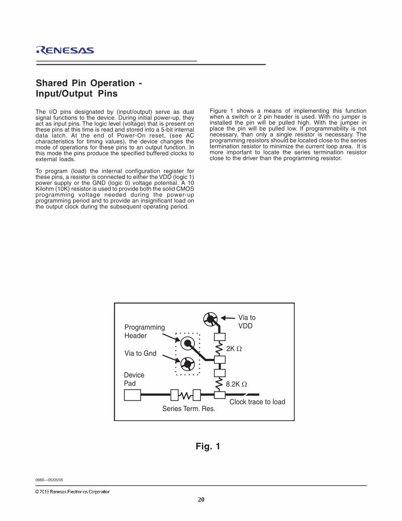
Fig. 1
Shared Pin Operation -Input/Output Pins
The I/O pins designated by (input/output) serve as dualsignal functions to the device. During initial power-up, theyact as input pins. The logic level (voltage) that is present onthese pins at this time is read and stored into a 5-bit internaldata latch. At the end of Power-On reset, (see ACcharacteristics for timing values), the device changes themode of operations for these pins to an output function. Inthis mode the pins produce the specified buffered clocks toexternal loads.
To program (load) the internal configuration register forthese pins, a resistor is connected to either the VDD (logic 1)power supply or the GND (logic 0) voltage potential. A 10Kilohm (10K) resistor is used to provide both the solid CMOSprogramming voltage needed during the power-upprogramming period and to provide an insignificant load onthe output clock during the subsequent operating period.
Via toVDD
Clock trace to loadSeries Term. Res.
ProgrammingHeader
Via to Gnd
DevicePad
2K
8.2K
Figure 1 shows a means of implementing this functionwhen a switch or 2 pin header is used. With no jumper isinstalled the pin will be pulled high. With the jumper inplace the pin will be pulled low. If programmability is notnecessary, than only a single resistor is necessary. Theprogramming resistors should be located close to the seriestermination resistor to minimize the current loop area. It ismore important to locate the series termination resistorclose to the driver than the programming resistor.

21
IntegratedCircuitSystems, Inc.
ICS951402Advance Information
0660—05/05/05
The impact of asserting the PCI_STOP# signal will be the following. All PCI and stoppable PCI_F clocks will latch low in theirnext high to low transition. The PCI_STOP# setup time tsu is 10 ns, for transitions to be recognized by the next rising edge.
PCI_STOP#
PCI_F 33MHz
PCI 33MHz
tsu
Assertion of PCI_STOP# Waveforms
PCI_STOP# - Assertion (transition from logic "1" to logic "0")
CPU_STOP#
CPUT
CPUC
The impact of asserting the CPU_STOP# pin is all CPU outputs that are set in the I2C configuration to be stoppable viaassertion of CPU_STOP# are to be stopped after their next transition following the two CPU clock edge sampling as shown.The final state of the stopped CPU signals is CPUT=High and CPUC=Low. There is to be no change to the output drive currentvalues. The CPUT will be driven high with a current value equal to (MULTSEL0) X (I REF), the CPUC signal will not be driven.
CPU_STOP# - Assertion (transition from logic "1" to logic "0")
Assertion of CPU_STOP# Waveforms

22
IntegratedCircuitSystems, Inc.
ICS951402Advance Information
0660—05/05/05
MIN MAX MIN MAXA -- 1.20 -- .047A1 0.05 0.15 .002 .006A2 0.80 1.05 .032 .041b 0.17 0.27 .007 .011c 0.09 0.20 .0035 .008DEE1 6.00 6.20 .236 .244eL 0.45 0.75 .018 .030Na 0° 8° 0° 8°
aaa -- 0.10 -- .004
VARIATIONS
MIN MAX MIN MAX48 12.40 12.60 .488 .496
10-0039
ND mm. D (inch)
Reference Doc.: JEDEC Publication 95, MO-153
0.50 BASIC 0.020 BASIC
SEE VARIATIONS SEE VARIATIONS
SEE VARIATIONS SEE VARIATIONS8.10 BASIC 0.319 BASIC
6.10 mm. Body, 0.50 mm. Pitch TSSOP (240 mil) (20 mil)
SYMBOLIn Millimeters In Inches
COMMON DIMENSIONS COMMON DIMENSIONS
INDEX
AREA
INDEX
AREA
1 21 2
N
D
E1 E
SEATING
PLANE
SEATING
PLANE
A1
AA2
e
- C -- C -
b
c
L
aaa C
Ordering Information
ICS951402yGLF-TExample:
Designation for tape and reel packaging
Annealed Lead Free (Optional)
Package Type G = TSSOP
Revision Designator (will not correlate with datasheet revision)
Device Type
Prefix ICS = Standard Device
ICS XXXX y G LF- T

23
IntegratedCircuitSystems, Inc.
ICS951402Advance Information
0660—05/05/05
INDEXAREAINDEXAREA
1 2
N
Dh x 45°
E1 E
α
SEATINGPLANESEATINGPLANE
A1
A
e
- C -
b
.10 (.004) C.10 (.004) C
c
L MIN MAX MIN MAXA 2.41 2.80 .095 .110A1 0.20 0.40 .008 .016b 0.20 0.34 .008 .0135c 0.13 0.25 .005 .010DE 10.03 10.68 .395 .420E1 7.40 7.60 .291 .299eh 0.38 0.64 .015 .025L 0.50 1.02 .020 .040Na 0° 8° 0° 8°
VARIATIONS
MIN MAX MIN MAX48 15.75 16.00 .620 .630
10-0034
0.635 BASIC 0.025 BASIC
COMMON DIMENSIONSIn Millimeters In Inches
COMMON DIMENSIONS
Reference Doc.: JEDEC Publication 95, MO-118
300 mil SSOP
N
SEE VARIATIONS SEE VARIATIONS
D mm. D (inch)
SYMBOL
SEE VARIATIONS SEE VARIATIONS
Ordering Information
ICS951402yFLF-TExample:
Designation for tape and reel packaging
Annealed Lead Free (Optional)
Package Type F = SSOP
Revision Designator (will not correlate with datasheet revision)
Device Type
Prefix ICS = Standard Device
ICS XXXX y F LF- T

Corporate HeadquartersTOYOSU FORESIA, 3-2-24 Toyosu,Koto-ku, Tokyo 135-0061, Japanwww.renesas.com
Contact InformationFor further information on a product, technology, the most up-to-date version of a document, or your nearest sales office, please visit:www.renesas.com/contact/
TrademarksRenesas and the Renesas logo are trademarks of Renesas Electronics Corporation. All trademarks and registered trademarks are the property of their respective owners.
IMPORTANT NOTICE AND DISCLAIMER
RENESAS ELECTRONICS CORPORATION AND ITS SUBSIDIARIES (“RENESAS”) PROVIDES TECHNICAL SPECIFICATIONS AND RELIABILITY DATA (INCLUDING DATASHEETS), DESIGN RESOURCES (INCLUDING REFERENCE DESIGNS), APPLICATION OR OTHER DESIGN ADVICE, WEB TOOLS, SAFETY INFORMATION, AND OTHER RESOURCES “AS IS” AND WITH ALL FAULTS, AND DISCLAIMS ALL WARRANTIES, EXPRESS OR IMPLIED, INCLUDING, WITHOUT LIMITATION, ANY IMPLIED WARRANTIES OF MERCHANTABILITY, FITNESS FOR A PARTICULAR PURPOSE, OR NON-INFRINGEMENT OF THIRD PARTY INTELLECTUAL PROPERTY RIGHTS.
These resources are intended for developers skilled in the art designing with Renesas products. You are solely responsible for (1) selecting the appropriate products for your application, (2) designing, validating, and testing your application, and (3) ensuring your application meets applicable standards, and any other safety, security, or other requirements. These resources are subject to change without notice. Renesas grants you permission to use these resources only for development of an application that uses Renesas products. Other reproduction or use of these resources is strictly prohibited. No license is granted to any other Renesas intellectual property or to any third party intellectual property. Renesas disclaims responsibility for, and you will fully indemnify Renesas and its representatives against, any claims, damages, costs, losses, or liabilities arising out of your use of these resources. Renesas' products are provided only subject to Renesas' Terms and Conditions of Sale or other applicable terms agreed to in writing. No use of any Renesas resources expands or otherwise alters any applicable warranties or warranty disclaimers for these products.
(Rev.1.0 Mar 2020)
© 2020 Renesas Electronics Corporation. All rights reserved.