programmable peripheral interface (ppi) -8255 · 2019-11-06 · programmable peripheral interface...
TRANSCRIPT
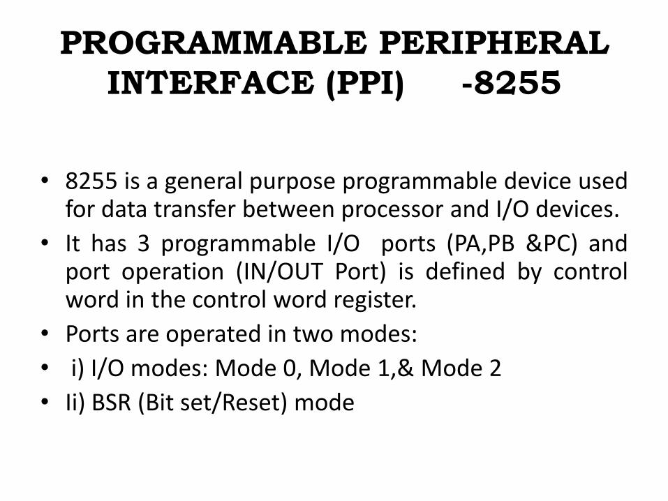
PROGRAMMABLE PERIPHERAL
INTERFACE (PPI) -8255
• 8255 is a general purpose programmable device usedfor data transfer between processor and I/O devices.
• It has 3 programmable I/O ports (PA,PB &PC) andport operation (IN/OUT Port) is defined by controlword in the control word register.
• Ports are operated in two modes:
• i) I/O modes: Mode 0, Mode 1,& Mode 2
• Ii) BSR (Bit set/Reset) mode

About 8255
• PPI has 40 pins and it has three distinct modes ofoperation.
• Port A (PA7-PA0) :8 pins
• Port B (PB7-PB0) :8 pins
• Port C (Pc: Upper: PC7-PC4) : 4 pins
• Port C (Pc: Lower: PC3-PC)) : 4 pins
• Data Bus (D7-D0) : 8 pins
• Control signals : 6 pins
• VCC and Gnd : 2 pins
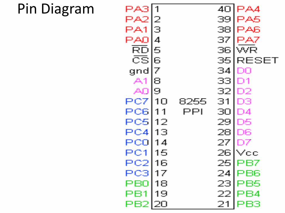
Pin Diagram
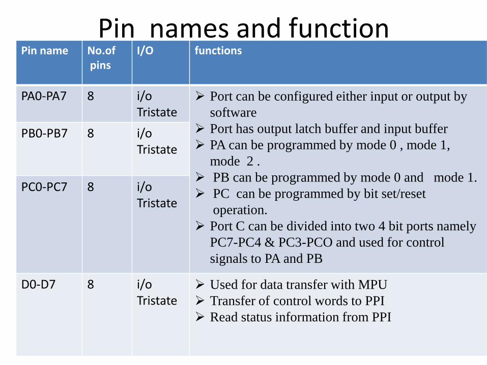
Pin names and functionPin name No.of
pinsI/O functions
PA0-PA7 8 i/o Tristate
Port can be configured either input or output by
software
Port has output latch buffer and input buffer
PA can be programmed by mode 0 , mode 1,
mode 2 .
PB can be programmed by mode 0 and mode 1.
PC can be programmed by bit set/reset
operation.
Port C can be divided into two 4 bit ports namely
PC7-PC4 & PC3-PCO and used for control
signals to PA and PB
PB0-PB7 8 i/o Tristate
PC0-PC7 8 i/o Tristate
D0-D7 8 i/o Tristate
Used for data transfer with MPU
Transfer of control words to PPI
Read status information from PPI

8255 Block Diagram


Group A and Group B control:
Group A and B get the Control Signal from CPU and send the command to the
individual control blocks.
Group A send the control signal to port A and Port C (Upper) PC7-PC4.
Group B send the control signal to port B and Port C (Lower) PC3-PC0.

• FOR I/O MODE:
The control word mode format for I/O as shown in figure
D7 D6 D5 D4 D3 D2 D1 D0
Group A
Port C Upper
1=Input
0=Output
Port A
1=Input
0=Output
Mode selection
00=mode 0
01=mode 1
1x=mode 2
Group B
Port C Lower
1=Input
0=Output
Port B
1=Input
0=Output
Mode selection
0=mode 0
1=mode 1
Mode set
1: i/o MODE
0: BSR mode

operation modes: i) I/O modes (M0,M1,&M2) ii) BSR (Bit set/Reset) mode
BIT SET/RESET MODE:The PORT C can be Set or Reset by sending OUT instruction to the CONTROL registers.
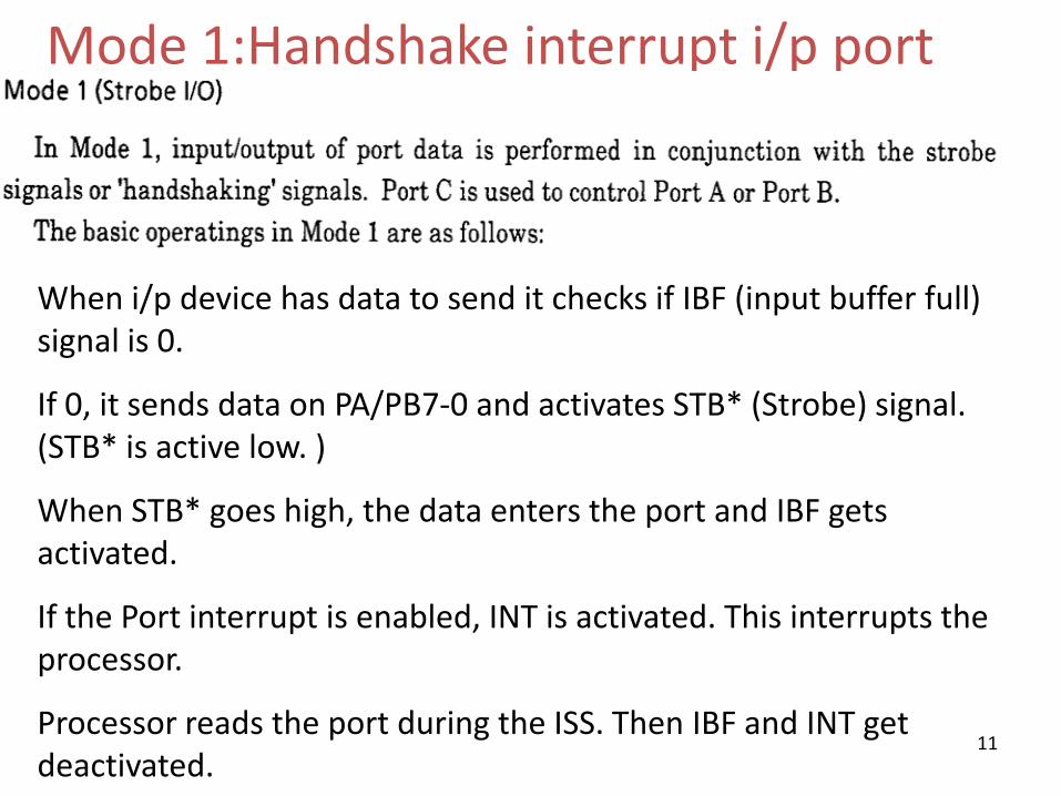
Mode 1:Handshake interrupt i/p port
When i/p device has data to send it checks if IBF (input buffer full) signal is 0.
If 0, it sends data on PA/PB7-0 and activates STB* (Strobe) signal. (STB* is active low. )
When STB* goes high, the data enters the port and IBF gets activated.
If the Port interrupt is enabled, INT is activated. This interrupts the processor.
Processor reads the port during the ISS. Then IBF and INT get deactivated.
11

82C55: Mode 1 Strobed Input
INTE A Controlled by bit set / reset of PC4. INTE B Controlled by bit set / reset of PC2.

Handshake interrupt o/p portWhen o/p device wants to receive data it checks if OBF* (output buffer full) signal is 0.
If 0, it receives data on PB7-0 and activates ACK* (Acknowledge) signal. ACK* is active low.
When ACK* goes high, the data goes out of the port and OBF* is set to 1.
If the Port interrupt is enabled, INT is activated. This interrupts the processor.
Processor sends another byte to the port during the ISS. Then OBF* and INT are reset to 0.
13
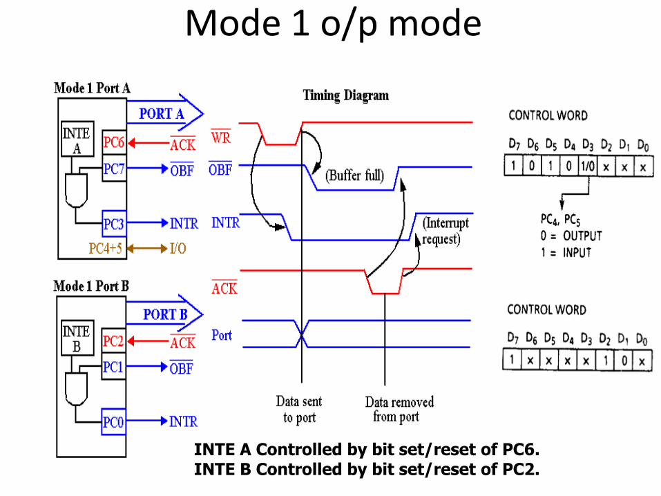
Mode 1 o/p mode
INTE A Controlled by bit set/reset of PC6. INTE B Controlled by bit set/reset of PC2.

82C55: Mode 2 Bi-directional Operation:


82C55: Mode 2 Bi-directional Operation
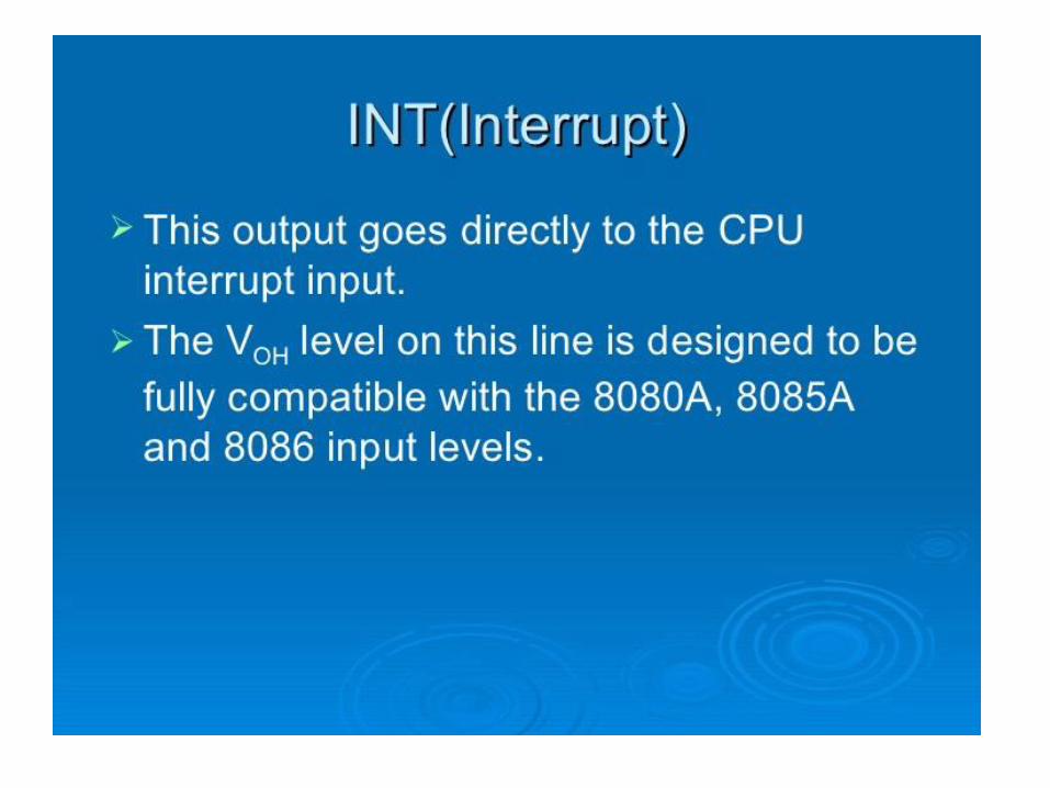
• INTR : Interrupt request is an output that requests an interrupt.
• ~OBF : Output Buffer Full is an output indicating that that output buffer contains data for the bi-directional bus.
• ~ACK : Acknowledge is an input that enables tri-state buffers which are otherwise in their high-impedance state.
• ~STB : The strobe input loads data into the port A latch.

82C55: Mode 2 Bi-directional Operation
• IBF : Input buffer full is an output indicating that the input latch contains information for the external bi-directional bus.
• INTE : Interrupt enable are internal bits that enable the INTR pin. BIT PC6(INTE1) and PC4(INTE2).
• PC2,PC1,PC0 : These port C pins are general-purpose I/O pins that are available for any purpose.

FOR BIT SET/RESET MODE (Port C only)
• This is bit set/reset control word format.
X X X
Don’t care
Bit select for Port C (Pc0-Pc7)
B0
B1
B2
D7 D6 D5 D4 D3 D2 D1 D0
0 1 2 3 4 5 6 7
0 1 0 1 0 1 0 1
0 0 1 1 0 0 1 1
0 0 0 0 1 1 1 1
BIT SET/RESET1=SET0=RESET
BIT SET/RESET FLAG=0 Active

• The control word for both mode is same.
• Bit D7 is used for specifying whether word loaded in to Bit set/reset mode or Mode definition word.
• D7=1=Mode definition mode.
• D7=0=Bit set/Reset mode.
• PC0-PC7 is set or reset as per the status of D0.
• A BSR word is written for each bit
• Example:
• PC3 is Set then control register will be 0XXX0111.
• PC4 is Reset then control register will be 0XXX01000.
• X is a don’t care.


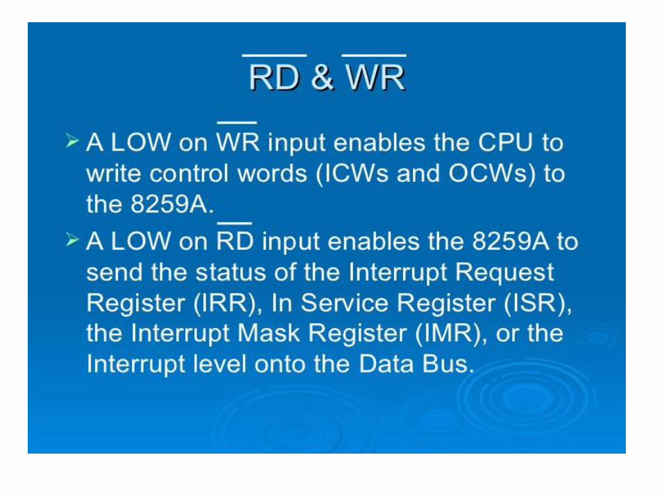
8259A PROGRAMMABLE
INTERRUPT CONTROLLER


8259A PIC FEATURES• Manage 8 interrupts according to the instructions
written into the control registers
• Vector location can be assigned anywhere in the
memory map. However all the 8 interrupts are
spaced at an interval of four to eight locations.
• Resolve 8 levels of interrupt priorities in variety of
modes.
• Be expanded to 64 priority levels by cascading
additional 8259As.
• Compatible with 8-bit as well as 16-bit processors.

8259A PIC- PIN DIGRAM

8259A PIC- BLOCK DIAGRAM


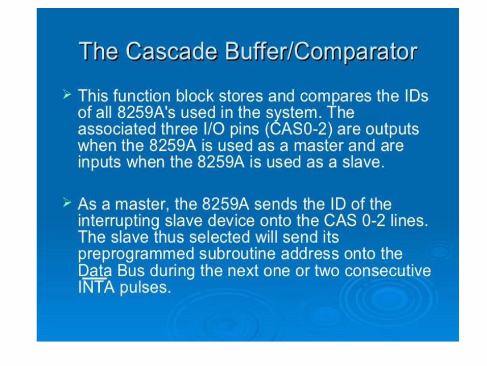

8259A PIC- CASCADE BUFFER/ COMPARATOR
Slave Program/ Enable Buffer:
• Used to specify whether 8259 is to act as a
master or a slave
High Master
Low Slave
• In Non-Buffered Mode, this pin is used to specify
whether 8259 is to act as a master or a slave.
• In Buffered mode this pin is used as an output to
enable the data bus buffer of the system.

8259A- Priority ModesFULLY NESTED MODE:
• General purpose mode.
• All IRs are arranged from highest to lowest.
• IR0 Highest IR7Lowest
• In addition any IR can be assigned the HP in this mode; the priority sequence will then begin at that IR
IR0 IR1 IR2 IR3 IR4 IR5 IR6 IR7
4 5 6 7
(LP)
0
(HP)
1 2 3

AUTOMATIC ROTATION MODE:
• In this mode, a device after being serviced, receivesthe lowest priority.
• Assuming that the IR2 has just been serviced, it willreceive the 7th priority
SPECIFIC ROTATION MODE:
• Similar to automatic rotation mode, except that the user can select any IR for the lowest priority, thus fixing all other priorities.
IR0 IR1 IR2 IR3 IR4 IR5 IR6 IR7
5 6 7 0 1 2 3 4

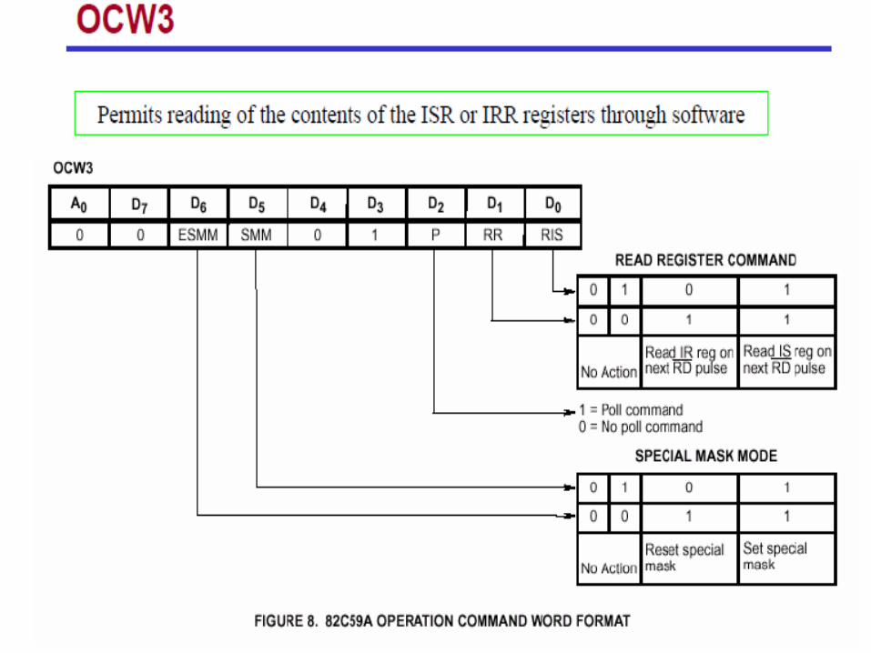
End of Interrupt (EOI)
• After the completion of interrupt service, the corresponding
ISR bit needs to be reset to update the information in the ISR.
This is called EOI command. It can be issued in three formats.
• Non Specific EOI: When this command send to the 8259 PIC,
it resets the highest priority ISR bit.
• Specific EOI: This command specifies which ISR bit to reset
• Automatic EOI: In this mode no command is necessary.
During the third INTA* the ISR bit is reset.
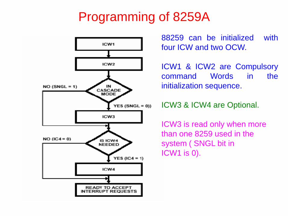
Programming of 8259A
88259 can be initialized with
four ICW and two OCW.
ICW1 & ICW2 are Compulsory
command Words in the
initialization sequence.
ICW3 & ICW4 are Optional.
ICW3 is read only when more
than one 8259 used in the
system ( SNGL bit in
ICW1 is 0).

For 8086 Don’t Care
ADI=1 for 8086 based system
p


8253/8254 Programmable counter / timer
• The Intel 8253 and 8254 are Programmable Interval
Timers (PITs), which perform timing and counting
functions using three 16-bit counters.
• Compatible with 8085/86 processor.
• The Intel 82c54 variant handles up to 10 MHz clock
signals.
• The timer interrupt is usually assigned to IRQ-0 (highest
priority hardware interrupt) because of the critical
function it performs and because so many devices
depend on it.


Intel 8253/54 : Programmable counter / timer
chip

3 counters ;Counter #0, #1, #2
• Each counter is identical, and each consists of a 16-bit,pre-settable, down counter.
• Each is fully independent and can be easily read by theCPU.
• Each counter is operated simultaneously but in differentmode condition (M0,M1,M2,M3,M4, & M5)
• When the counter is read, the data within the counter willnot be disturbed.
• This allows the system or your own program to monitorthe counter's value at any time, without disrupting theoverall function of the 8253.

Data Bus: This tri-state, bi-directional, 8-bit buffer is
used to interface the 8253/54 to the system data bus.
The Data bus buffer has three basic functions.
• 1. Programming the modes of 8253/54.
• 2. Loading the count registers.
• 3. Reading the count values
A1 A0 Operation
0 0 Counter 0
0 1 Counter 1
1 0 Counter 2
1 1 Control word register

Counter operationTo operate a counter, a desired 16-bit count is loaded in its
register and, on command, it begins to decrement the count until
it reaches 0. At the end of the count, it generates a pulse that can
be used to interrupt the CPU.
Control Word Register (CWR)
• This internal register is used to write information to, prior to using
the device.
• This register is addressed when A0 and A1 inputs are logical 1's.
• The data in the register controls the operation mode and the
selection of either binary or BCD ( binary coded decimal )
counting format.
• The register can only be written to. You can't read information
from the register.

Programming of 8253 (CWR)

Read operation (performed by CPU)In event counters, it is necessary to read the value of the count in process.
This is done by three methods
• Simple read operation (Rw1: Rw2)
• Counter Latch Command (RW1/Rw2:0/0;
• Read Back command ( Available in 8254)

CWR for read back command

Counter status format

Modes of opertaion
• Mode 0 Interrupt on terminal count
• Mode 1 H/W retriggerable one shot
• Mode 2 Rate generator
• Mode 3 Square wave generator
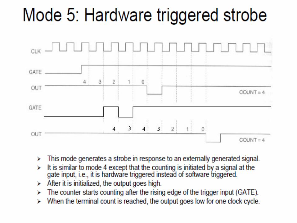
• Mode 4 S/W triggered strobe
• Mode 5 H/W triggered strobe

`The OUT pin is set low after the Control Word is written, and counting
starts one clock cycle after the COUNT programmed. OUT remains low
until the counter reaches 0, at which point OUT will be set high until the
counter is reloaded or the Control Word is written.
The Gate signal should remain active high for normal counting. If Gate
goes low counting gets terminated and current count is latched till Gate
pulse goes high again.

In this mode 8253 can be used as Monostable Multivibrator. GATE
input is used as trigger input.
OUT will be initially high. OUT will go low on the Clock pulse
following a trigger to begin the one-shot pulse, and will remain low
until the Counter reaches zero. OUT will then go high and remain
high until the CLK pulse after the next trigger.

In this mode, the device acts as a divide-by-n counter, which is commonly
used to generate a real-time clock interrupt.
Like other modes, counting process will start the next clock cycle after COUNT
is sent. OUT will then remain high until the counter reaches 1, and will go low
for one clock pulse. OUT will then go high again, and the whole process
repeats itself.


8237DMA CONTROLLER
IIE - SAP

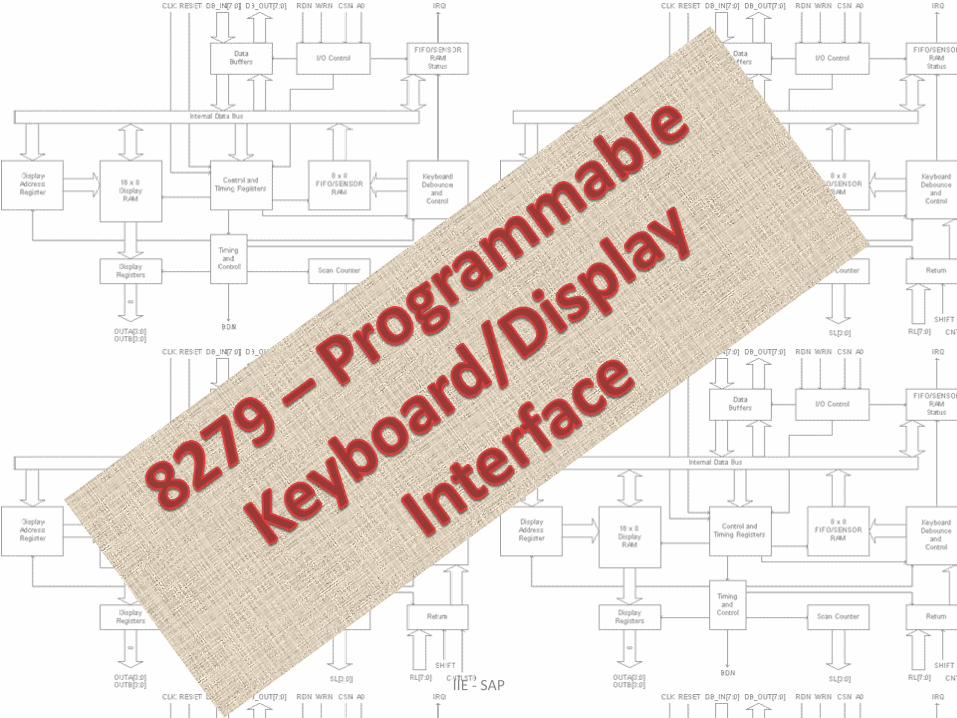
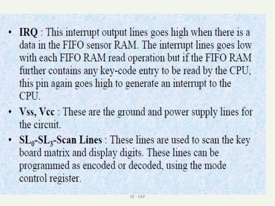
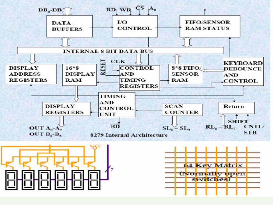
The keyboard display controller chip 8279 provides
A set of four scan lines and eight return lines for interfacing keyboard
A set of eight output lines for interfacing display.
Scan line are used to drive multiplexed 7 segment display
IIE - SAP
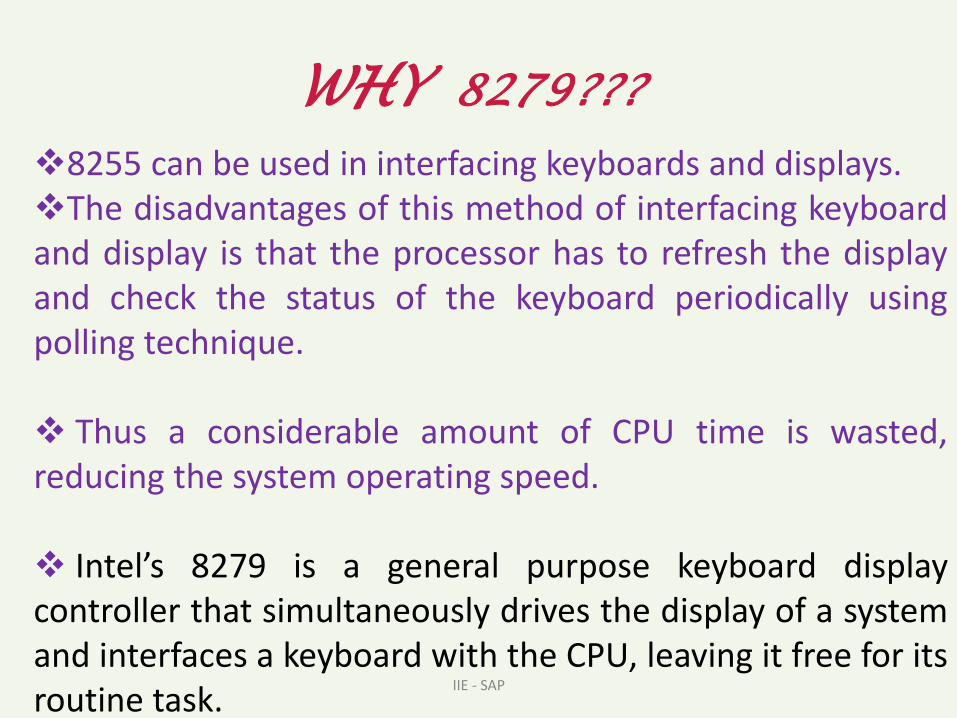
WHY 8279???
8255 can be used in interfacing keyboards and displays.The disadvantages of this method of interfacing keyboardand display is that the processor has to refresh the displayand check the status of the keyboard periodically usingpolling technique.
Thus a considerable amount of CPU time is wasted,reducing the system operating speed.
Intel’s 8279 is a general purpose keyboard displaycontroller that simultaneously drives the display of a systemand interfaces a keyboard with the CPU, leaving it free for itsroutine task.
IIE - SAP

IIE - SAP

IIE - SAP

IIE - SAP
IIE - SAP

IIE - SAP

IIE - SAP

IIE - SAP
IIE - SAP

8279
Keyboard segment
i)Scans the keyboard
ii) detects key if any key is pressed
iii) Key code is stored in 8x8 FIFO RAM
iv) data in FIFO RAM sends Interrupt signal to CPU
vi) CPU reads the key code stored in FIFO RAM
Display segment
vii) Then CPU writes the key code in 16x8 display RAM
viii)Display devices display the data in the display RAM
IIE - SAP

BLOCK
DIA
8279
KEYBOARD
i) Scanned Keyboard ( 2 Key lock out /N key roll over)
ii)strobed input mode
iii)scanned sensor matrix mode
SCAN
i) Encoded
ii) Decoded
MUX. DISPLAY (8 digit or 16 digit)
i)Left Entry
ii) Right Entry
MPU INTERFACE
IIE - SAP

IIE - SAP
2 Key lock out/N key roll overKEY DEBOUNCEWhen a key is pressed, a debounce logic comes into operation. ReturnBuffers and Keyboard De-bounce and Control section scans for a key closurerow wise. If a key closer is detected, the keyboard debounce unit debouncesthe key entry (i.e. wait for 10 ms).
When a key is pressed, a debounce logic comes into operation. After thedebounce period (i.e. wait for 10 ms). , if the key continues to be detected,The code of key is directly transferred to the sensor RAM along with SHIFTand CONTROL key status.2 key lock out: If two keys are pressed simultaneously within a debouncecycle, no key is recognized and no key code is stored in FIFO RAM till one ofthem remains closed and the other is released.N – key roll overAny number of keys can be pressed simultaneously and recognized in theorder, the keyboard scan recorded them. All the codes of such keys areentered into FIFO.In this mode, the first pressed key need not be released before the second ispressed.

• CNTL/STB i/p mode:, control lines that enters data in FIFORAM . Shift: The status of shift is stored along with key code inFIFO RAM .
• In Scanned Sensor Matrix mode, a sensor array can beinterfaced with 8279 using either encoded or decoded scansto scan the key matrix and refresh the display.
IIE - SAP

Output (Display) Modes : 8279 provides two output modes for selecting the display options.
Display Scan :
• In this mode 8279 provides 8 or 16 character multiplexed displays those can be organized as dual 4- bit or single 8-bit display units.
Display Entry
( right entry or left entry mode )
• 8279 allows options for data entryon the displays.
• The display data is entered fordisplay either from the right side orfrom the left side.
IIE - SAP

Control and Timing Register and Timing Control • These registers store the keyboard and display modes and
other operating conditions programmed by CPU.
IIE - SAP
The registers are written with A0=1 and WR=0.The Timing and control unit controls the basic timings forthe operation of the circuit.

All the command words or status words are written orread with A0 = 1 and CS = 0 to or from 8279.
a) Keyboard Display Mode Set : The format of the command word to select different modes of operation of 8279 is given below with its bit definitions.
D7 D6 D5 D4 D3 D2 D1 D0
0 0 0 D D K K K
IIE - SAP

SENSOR MATRIX
SENSOR MATRIX
IIE - SAP
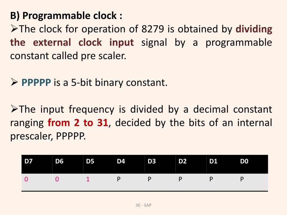
B) Programmable clock : The clock for operation of 8279 is obtained by dividingthe external clock input signal by a programmableconstant called pre scaler.
PPPPP is a 5-bit binary constant.
The input frequency is divided by a decimal constantranging from 2 to 31, decided by the bits of an internalprescaler, PPPPP.
D7 D6 D5 D4 D3 D2 D1 D0
0 0 1 P P P P P
IIE - SAP
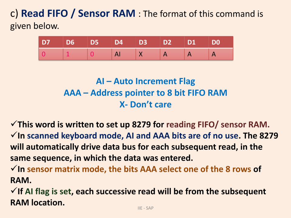
c) Read FIFO / Sensor RAM : The format of this command is given below.
AI – Auto Increment FlagAAA – Address pointer to 8 bit FIFO RAM
X- Don’t care
This word is written to set up 8279 for reading FIFO/ sensor RAM. In scanned keyboard mode, AI and AAA bits are of no use. The 8279 will automatically drive data bus for each subsequent read, in the same sequence, in which the data was entered.In sensor matrix mode, the bits AAA select one of the 8 rows of RAM. If AI flag is set, each successive read will be from the subsequent RAM location.
D7 D6 D5 D4 D3 D2 D1 D0
0 1 0 AI X A A A
IIE - SAP

d) Read Display RAM : This command enables a programmer to read the display RAM data.
The CPU writes this command word to 8279 to prepare it for display RAM read operation. AI is auto increment flag and AAAA, the 4-bit address points to the 16-byte display RAM that is to be read.If AI=1, the address will be automatically, incremented after each read or write to the Display RAM. The same address counter is used for reading and writing.
D7 D6 D5 D4 D3 D2 D1 D0
0 1 1 AI A A A A
IIE - SAP
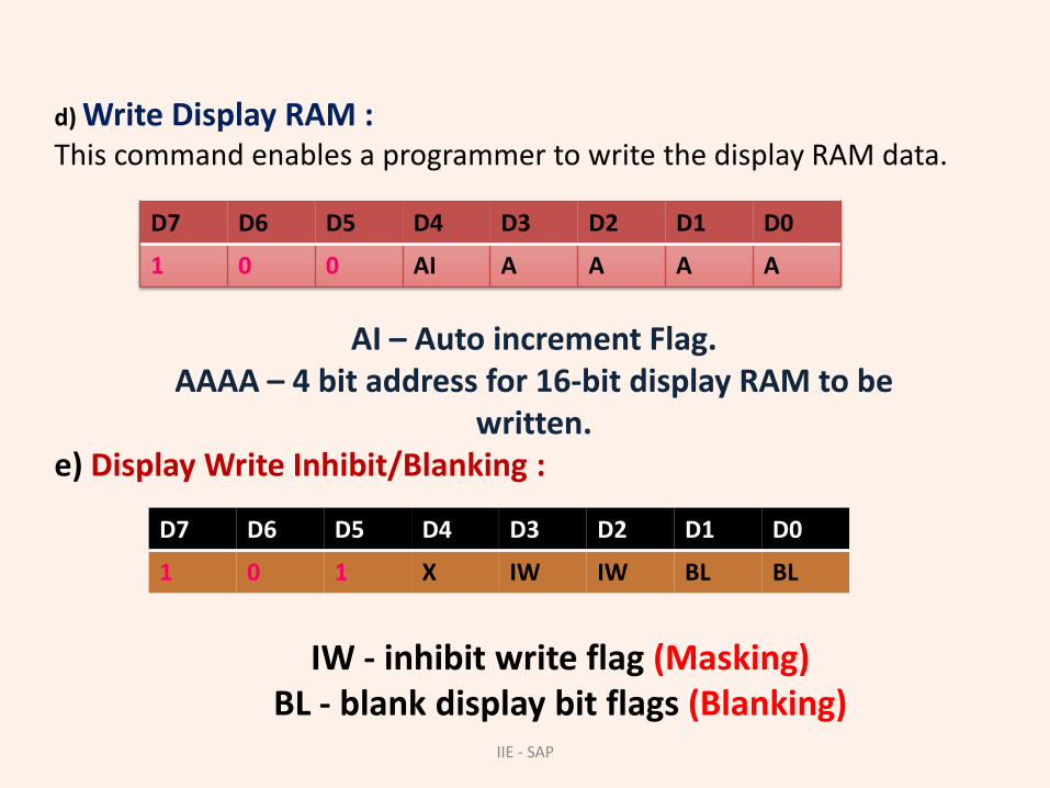
d) Write Display RAM : This command enables a programmer to write the display RAM data.
AI – Auto increment Flag.AAAA – 4 bit address for 16-bit display RAM to be
written.e) Display Write Inhibit/Blanking :
D7 D6 D5 D4 D3 D2 D1 D0
1 0 0 AI A A A A
D7 D6 D5 D4 D3 D2 D1 D0
1 0 1 X IW IW BL BL
IW - inhibit write flag (Masking) BL - blank display bit flags (Blanking)
IIE - SAP

g) Clear Display RAM :
CD: CLEAR DISPLAY ; CF: CLEAR FIFO RAM STATUS; CA: CLEAR ALL (both CD&CF)
D7 D6 D5 D4 D3 D2 D1 D0
1 1 0 CD2 CD1 CD0 CF CA
IIE - SAP

h) End Interrupt / Error mode Set :
E- Error modeX- don’t care
For the sensor matrix mode, this command lowers the IRQ line and enables further writing into the RAM. Otherwise, if a change in sensor value is detected, IRQ goes high that inhibits writing in the sensor RAM. For N-Key roll over mode, if the E bit is programmed to be ‘1’, the 8279 operates in special Error mode
D7 D6 D5 D4 D3 D2 D1 D0
1 1 1 E X X X 1
IIE - SAP

I/O Interface
FIFO status register
•Code given in text for reading keyboard.
•Data returned from 8279 contains raw data that need to be translated to ASCII:
IIE - SAP

IIE - SAP

ADC 0809

ADC 0809• The ADC0809 is an 8-bit successive approximation type
ADC with inbuilt 8-channel multiplexer.
• The ADC0809 is suitable for interface with 8086
microprocessor.
• The ADC0809 is available as a 28 pin IC in DIP (Dual Inline
Package).
• The ADC0809 has a total unadjusted error of ±1 LSD (Least
Significant Digit).

PIN DESCRIPTION OF
ADC0809

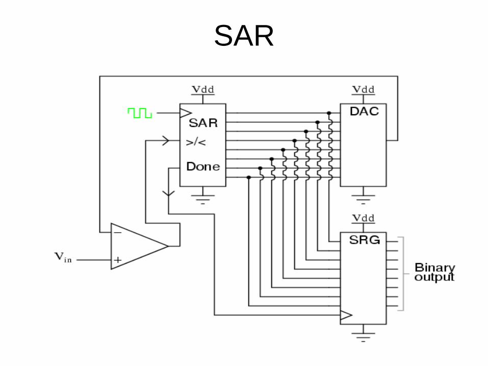
SAR

Interfacing ADC with 8085 thro 8255

ADC interfacing with 8051

DAC• To convert the digital signal to analog signal a Digital-to-Analog Converter
(DAC) has to be employed. ( binary weighted and R/2R ladder. )
• The DAC will accept a digital (binary) input and convert to analog voltage
or current.
• Every DAC will have "n" input lines and an analog output.
• The DAC require a reference analog voltage (Vref) or current (Iref)
source.
• The smallest possible analog value that can be represented by the n-bit
binary code is called resolution.
• The resolution of DAC with n-bit binary input is 1/2nof reference analog
value.

DAC 0800
•
The DAC0800 is an 8-bit, high speed, current output DAC with a typical
settling time (conversion time) of 100 ns.
• It produces complementary current output, which can be converted to
voltage by using simple resistor load.
• The DAC0800 require a positive and a negative supply voltage in the range
of ± 5V to ±18V.
• It can be directly interfaced with TTL, CMOS, PMOS and other logic
families.
• For TTL input, the threshold pin should be tied to ground (VLC = 0V).

R-2R Ladder

pin configuration of DAC0800

DAC interfacing with 8085 thro 8255

DAC interfacing with 8051