programmable current and voltage - analog devices v to 5.5 v, spi, unbuffered voltage output 12-bit...
TRANSCRIPT

4 mA TO 20 mACURRENT LOOP
ACTUATORCONTROL
SYSTEMCONTROLLER/PROCESSOR
nanoDACLOOP
INTERFACEDRIVER
CLEAR
AVDO GND
–VSENSE
CLRSEL
AVSS REFIN
VOUT
+VSENSE
REXT
CONTROL
AD5748/AD5750/AD5751
VIN
+
–
FAULT
POWER-ONRESET
RANGESCALING
LOGIC INTERFACE CRC-8 IOUTV-TO-I
VOLTAGE
OVERTEMPERATUREOPEN
SHORTRANGE
Programmable Current and Voltage Output Drivers Simplify Design of 4 mA to 20 mA Communication LoopsThe ever pressing need to maximize system productivity and overall system reliability within the industrial control environment is driving demand for high performance, highly configurable loop interface and actuation control solutions. ADI offers a complete portfolio of footprint and software-compatible loop interface drivers that set a new industry standard for performance and feature set. Designed to meet the communication needs of industrial control systems, ADI’s loop interface drivers offer easy to use, flexible solutions, which require minimum external components to realize specified performance.
The single-channel AD5750 can handle virtually all standard voltage and current analog output signaling requirements with selectable hardware or software programmability. Alternatively, the AD5749 caters to those who require standard current outputs only. Offering extensive self-diagnostic features, the AD5750 family provides a robust solution for single- and multichannel analog I/O systems, making troubleshooting quick and easy.
These drivers are ideally suited for use with ADI’s low voltage, single-supply nanoDAC® family (for example, AD5662, AD5664, AD5668), conditioning their output to provide the desired loop response. The low voltage analog output generated by ADI’s nanoDAC family interfaces effortlessly with the AD5750 family of drivers to reduce design complexity, enabling faster design cycles and reduced development cost.
Features
• Configurable voltage and current output ranges
• IOUT ranges: 4 mA to 20 mA, 0 mA to 20 mA, 0 mA to 24 mA, ±20 mA, and ±24 mA
• VOUT ranges: 0 V to 5 V, 0 V to 10 V, ±5 V, and ±10 V
• Threefold improvement in performance over competing offers with total unadjusted error (TUE) of ±0.08% FSR
• Extensive diagnostic features and output fault detection
• Configured via hardware or software
• High compliance voltage up to 55 V
• Extended temperature range from –40°C to +125°C
• Small package: 5 mm × 5 mm, 32-lead LFCSP
Loop interface driver solutions.
Output drivers for industrial designs.
Programmable Current and Voltage Output Drivers
www.analog.com/inamps
Industrial Output Driver ICs*Part Number
Output Type
Voltage Range (V) Current Range (mA)Input Voltage
Range (V)Description
AD5750Voltage or
current0 to 5, 0 to 10, ±5, ±10
with 20% overrange
4 to 20, 0 to 20, 0 to 24, ±20,
±24 with 2% overrange0 to 4.096
Bipolar current and voltage output driver with programmable ranges and analog input range
0 V to 4.096 V
AD5750-1Voltage or
current0 to 5, 0 to 10, ±5, ±10
with 20% overrange4 to 20, 0 to 24, ±20, ±24 with 2% overrange
0 to 2.5Bipolar current and voltage output driver with programmable ranges and analog input range
0 V to 2.5 V
AD5751Voltage or
current0 to 5, 0 to 10, 0 to 40 with 20% overrange
0 to 20, 0 to 24, 4 to 20 with 2% overrange
0 to 4.096Unipolar current and voltage output driver with
programmable ranges and 55 V compliance
AD5748Voltage or
current0 to 5, 0 to 10.5, ±10.5
with 20% overrange4 to 21,
0 to 21 with 2% overrange0 to 4.096
Current and voltage output driver with programmable ranges and analog input range
0 V to 4.096 V, 24 V compliance
AD5749 Current N/A0 to 24,
4 to 20 with 2% overrange0 to 4.096
Unipolar current output driver with programmable ranges and 55 V compliance
*Available in 32-lead LFCSP.
nanoDAC ConvertersPart Number
Channels Resolution Package Description
AD5512A 1 12 16-lead LFCSP2.7 V to 5.5 V, SPI, unbuffered voltage output 12-bit
DAC with 1 LSB INL and 1 µs settling time
AD5541A 1 1610-lead MSOP, 10-lead LFCSP,
8-lead LFCSP2.7 V to 5.5 V, SPI, unbuffered voltage output 16-bit DAC with
1 LSB INL and 1 µs settling time; AD5542A for bipolar operation
AD5620 1 12 8-lead SOT-23, 8-lead MSOP2.7 V to 5.5 V, SPI, rail-to-rail output DAC with
1.25 V/2.5 V, 5 ppm/°C reference
AD5660 1 16 8-lead SOT-23, 8-lead MSOP2.7 V to 5.5 V, SPI, rail-to-rail output DAC with
1.25 V/2.5 V, 5 ppm/°C referenceAD5662 1 16 8-lead SOT-23, 8-lead MSOP 2.7 V to 5.5 V, SPI, rail-to-rail output DAC
AD5623R 2 12 10-lead MSOP, 10-lead LFCSP2.7 V to 5.5 V, SPI, rail-to-rail output DAC with 1.25 V/2.5 V,
5 ppm/°C reference, LDAC and CLR pinAD5663/ AD5663R
2 16 10-lead MSOP, 10-lead LFCSP2.7 V to 5.5 V, SPI, rail-to-rail output DAC with LDAC and CLR
pin; AD5663R contains a 1.25 V/2.5 V, 5 ppm/°C referenceAD5624/ AD5624R
4 12 10-lead MSOP, 10-lead LFCSP2.7 V to 5.5 V, SPI, rail-to-rail output DAC. AD5624R
contains a 1.25 V/2.5 V, 5 ppm/°C reference
AD5664/ AD5664R
4 16 10-lead MSOP, 10-lead LFCSP2.7 V to 5.5 V, SPI, rail-to-rail output DAC. AD5664R
contains a 1.25 V/2.5 V, 5 ppm/°C reference
AD5628 8 12 16-lead TSSOP, 16-lead LFCSP2.7 V to 5.5 V, SPI, rail-to-rail output DAC with 1.25 V/2.5 V,
5 ppm/°C reference, LDAC and CLR pin
AD5668 8 16 16-lead TSSOP, 16-lead LFCSP2.7 V to 5.5 V, SPI, rail-to-rail output DAC with 1.25 V/2.5 V,
5 ppm/°C reference, LDAC and CLR pin
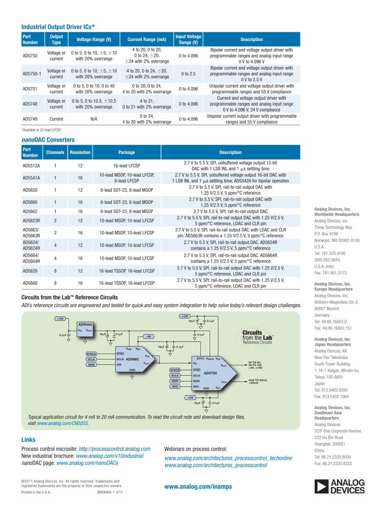
Circuits from the Lab™ Reference CircuitsADI’s reference circuits are engineered and tested for quick and easy system integration to help solve today’s relevant design challenges.
+
SCLK
VREF
VIN VOUT
VDD
VDD
VSS
10�F 0.1�F
VINVOUT
IOUT
VREFIN
VFB
VOUTDIN
DVCC
0V TO 5V,0V TO 10V±5V, ±10V
4mA TO 20mA,±20mA
GND
GND
AD5662
ADR444
AD5750
SYNC
SYNCB
SDIN
SCLK
SYNCA
SCLK
SDIN
SDO
–15V
SYNC
SCLK
SDIN
SDO
+10�F 0.1�F
0.1�F
+15V+15V
+5V
+10�F 0.1�F
+10�F 0.1�F0.1�F
Typical application circuit for 4 mA to 20 mA communication. To read the circuit note and download design files, visit www.analog.com/CN0203.
LinksProcess control microsite: http://processcontrol.analog.com New industrial brochure: www.analog.com/v10industrial nanoDAC page: www.analog.com/nanoDACs
Webinars on process control:
www.analog.com/architectures_processcontrol_techonline www.analog.com/architectures_processcontrol
www.analog.com/inamps
Analog Devices, Inc.Worldwide HeadquartersAnalog Devices, Inc. Three Technology Way P.O. Box 9106 Norwood, MA 02062-9106 U.S.A. Tel: 781.329.4700 (800.262.5643, U.S.A. only) Fax: 781.461.3113
Analog Devices, Inc. Europe HeadquartersAnalog Devices, Inc. Wilhelm-Wagenfeld-Str. 6 80807 Munich Germany Tel: 49.89.76903.0 Fax: 49.89.76903.157
Analog Devices, Inc. Japan HeadquartersAnalog Devices, KK New Pier Takeshiba South Tower Building 1-16-1 Kaigan, Minato-ku, Tokyo, 105-6891 Japan Tel: 813.5402.8200 Fax: 813.5402.1064
Analog Devices, Inc. Southeast Asia HeadquartersAnalog Devices 22/F One Corporate Avenue 222 Hu Bin Road Shanghai, 200021 China Tel: 86.21.2320.8000 Fax: 86.21.2320.8222
©2011 Analog Devices, Inc. All rights reserved. Trademarks and registered trademarks are the property of their respective owners.
Printed in the U.S.A. BR09468-1-3/11