prof. jorge kittl, dept. of physics and...
TRANSCRIPT
Back end Memories
Prof. Jorge Kittl,
Dept. of Physics and Astronomy

Outline
Introduction
STT-RAM
RRAM Systems
o OXRAM
o CBRAM
o Mott
Summary
2 Prof. Jorge Kittl, KU Leuven - EPICO 2012, Buenos Aires, Argentina

DRAM
SRAM
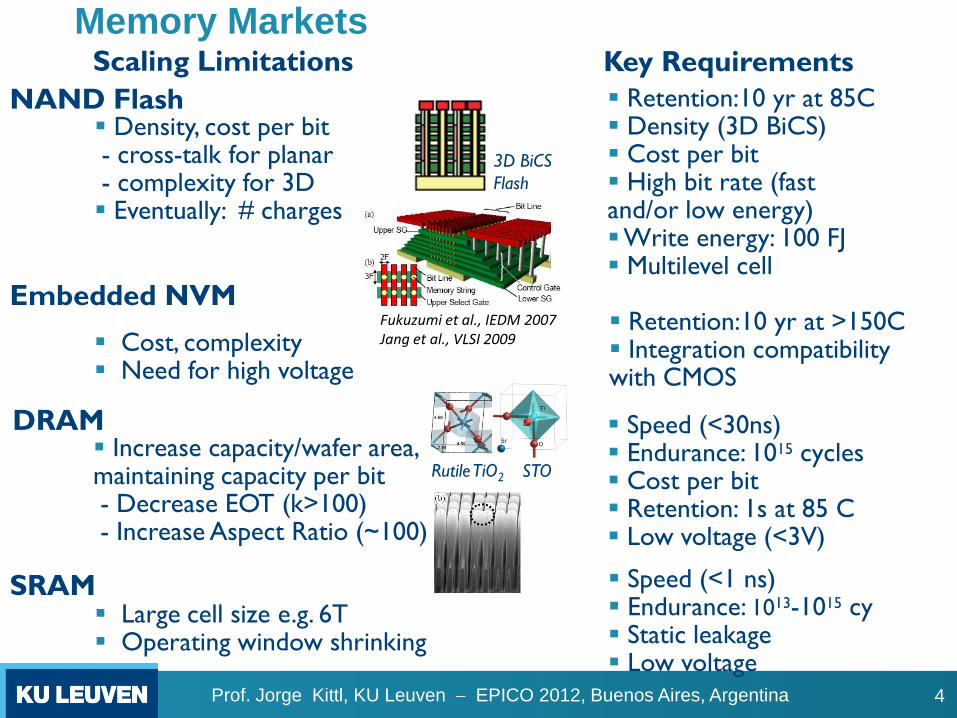
Density, cost per bit - cross-talk for planar - complexity for 3D Eventually: # charges
Cost, complexity Need for high voltage
Scaling Limitations
Large cell size e.g. 6T Operating window shrinking
Increase capacity/wafer area, maintaining capacity per bit - Decrease EOT (k>100) - Increase Aspect Ratio (~100)
Rutile TiO2
Ti
SrO
STO
Fukuzumi et al., IEDM 2007 Jang et al., VLSI 2009
3D BiCS
Flash
Embedded NVM
NAND Flash
Memory Markets
3 Prof. Jorge Kittl, KU Leuven - EPICO 2012, Buenos Aires, Argentina
DRAM
SRAM
Density, cost per bit - cross-talk for planar - complexity for 3D Eventually: # charges
Cost, complexity Need for high voltage
Scaling Limitations
Large cell size e.g. 6T Operating window shrinking
Increase capacity/wafer area, maintaining capacity per bit - Decrease EOT (k>100) - Increase Aspect Ratio (~100)
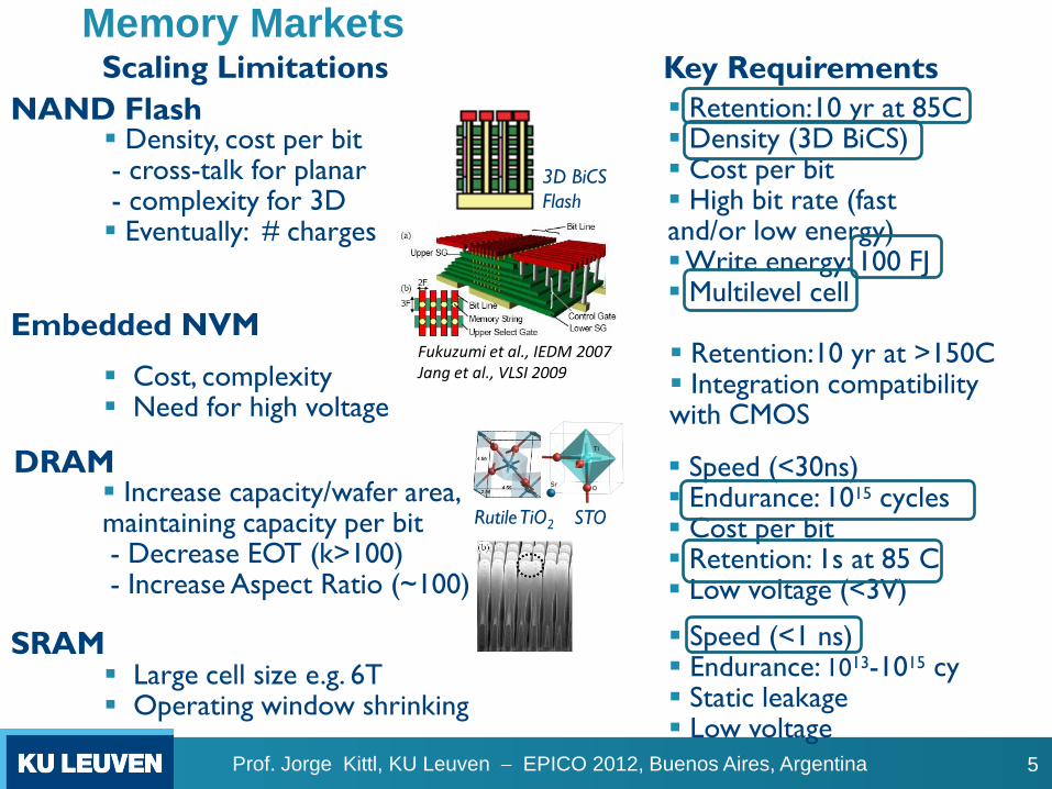
Retention:10 yr at 85C Density (3D BiCS) Cost per bit High bit rate (fast and/or low energy) Write energy: 100 FJ Multilevel cell
Retention:10 yr at >150C Integration compatibility with CMOS
Speed (<1 ns) Endurance: 1013-1015 cy Static leakage Low voltage
Speed (<30ns) Endurance: 1015 cycles Cost per bit Retention: 1s at 85 C Low voltage (<3V)
Key Requirements
Rutile TiO2
Ti
SrO
STO
Fukuzumi et al., IEDM 2007 Jang et al., VLSI 2009
3D BiCS
Flash
Embedded NVM
NAND Flash
Memory Markets
4 Prof. Jorge Kittl, KU Leuven - EPICO 2012, Buenos Aires, Argentina
DRAM
SRAM
Density, cost per bit - cross-talk for planar - complexity for 3D Eventually: # charges
Cost, complexity Need for high voltage
Scaling Limitations
Large cell size e.g. 6T Operating window shrinking
Increase capacity/wafer area, maintaining capacity per bit - Decrease EOT (k>100) - Increase Aspect Ratio (~100)
Retention:10 yr at 85C Density (3D BiCS) Cost per bit High bit rate (fast and/or low energy) Write energy: 100 FJ Multilevel cell
Retention:10 yr at >150C Integration compatibility with CMOS
Speed (<1 ns) Endurance: 1013-1015 cy Static leakage Low voltage
Speed (<30ns) Endurance: 1015 cycles Cost per bit Retention: 1s at 85 C Low voltage (<3V)
Key Requirements
Rutile TiO2
Ti
SrO
STO
Fukuzumi et al., IEDM 2007 Jang et al., VLSI 2009
3D BiCS
Flash
Embedded NVM
NAND Flash
Memory Markets
5 Prof. Jorge Kittl, KU Leuven - EPICO 2012, Buenos Aires, Argentina
DRAM
SRAM
Density, cost per bit - cross-talk for planar - complexity for 3D Eventually: # charges
Cost, complexity Need for high voltage
Scaling Limitations
Large cell size e.g. 6T Operating window shrinking
Increase capacity/wafer area, maintaining capacity per bit - Decrease EOT (k>100) - Increase Aspect Ratio (~100)
Retention:10 yr at 85C Density (3D BiCS) Cost per bit High bit rate (fast and/or low energy) Write energy: 100 FJ Multilevel cell
Retention:10 yr at >150C Integration compatibility with CMOS
Speed (<1 ns) Endurance: 1013-1015 cy Static leakage Low voltage
Speed (<30ns) Endurance: 1015 cycles Cost per bit Retention: 1s at 85 C Low voltage (<3V)
Key Requirements
Rutile TiO2
Ti
SrO
STO
Fukuzumi et al., IEDM 2007 Jang et al., VLSI 2009
3D BiCS
Flash
Embedded NVM
NAND Flash
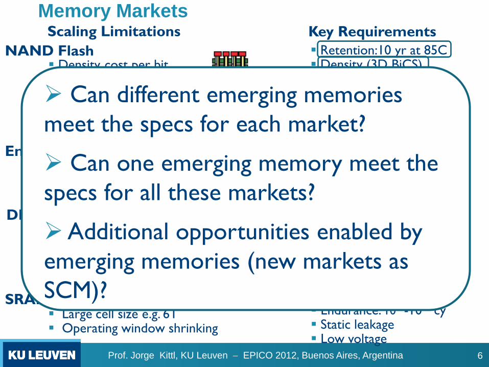
Can different emerging memories
meet the specs for each market?
Can one emerging memory meet the
specs for all these markets?
Additional opportunities enabled by
emerging memories (new markets as
SCM)?
Memory Markets
6 Prof. Jorge Kittl, KU Leuven - EPICO 2012, Buenos Aires, Argentina

Emerging “Back End” Memories
Amorphous Crystalline
High resistivity Low resistivity
Amorphous Crystalline
High resistivity Low resistivity
Crystalline
GST
Top
Electrode
Resistor
(heater)
Thermal
Insulator
(a/Xtalline
GST)
I
Bottom
Electrode
Data storage region
7 Prof. Jorge Kittl, KU Leuven - EPICO 2012, Buenos Aires, Argentina
Memory state stored as resistance state
Can switch between different resistance states
by electrical pulses
Several emerging memories have resistance
switching behavior:
Phase change RAM (PC-RAM)
Spin torque transfer RAM (STT-RAM)
RRAM OXRAM
CBRAM
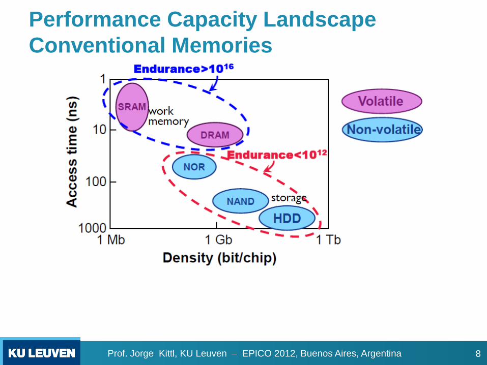
Performance Capacity Landscape
Conventional Memories
8 Prof. Jorge Kittl, KU Leuven - EPICO 2012, Buenos Aires, Argentina
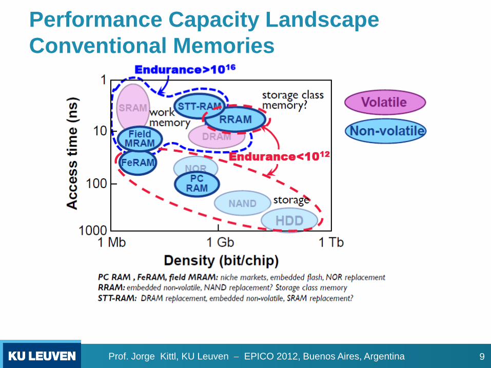
Performance Capacity Landscape
Conventional Memories
9 Prof. Jorge Kittl, KU Leuven - EPICO 2012, Buenos Aires, Argentina

Need for Selector: Density Implications
10 Prof. Jorge Kittl, KU Leuven - EPICO 2012, Buenos Aires, Argentina
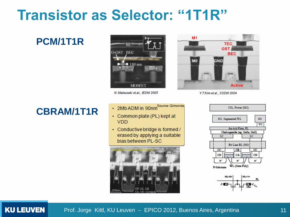
Transistor as Selector: “1T1R”
PCM/1T1R
CBRAM/1T1R
11 Prof. Jorge Kittl, KU Leuven - EPICO 2012, Buenos Aires, Argentina
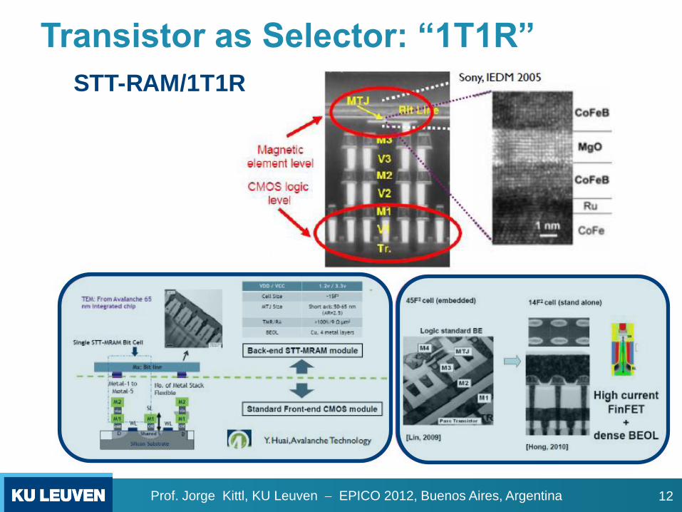
STT-RAM/1T1R
Transistor as Selector: “1T1R”
12 Prof. Jorge Kittl, KU Leuven - EPICO 2012, Buenos Aires, Argentina

OXRAM/1D1R
OTP/1D1R
2 Terminal Selector: “1D1R”
13 Prof. Jorge Kittl, KU Leuven - EPICO 2012, Buenos Aires, Argentina

Selector: Density Implications
1T1R
2 terminal selector “1D1R”3D stacked
6F2 4 F2 (VFET)
DRAM replacement
NAND replacement
3D bit cost savings (BICS)
14 Prof. Jorge Kittl, KU Leuven - EPICO 2012, Buenos Aires, Argentina
Outline
Introduction
STT-RAM
RRAM Systems
o OXRAM
o CBRAM
o Mott
Summary
15 Prof. Jorge Kittl, KU Leuven - EPICO 2012, Buenos Aires, Argentina
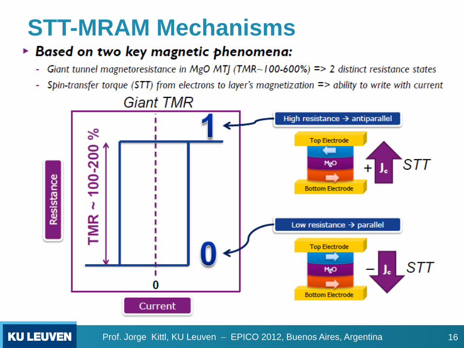
STT-MRAM Mechanisms
16 Prof. Jorge Kittl, KU Leuven - EPICO 2012, Buenos Aires, Argentina
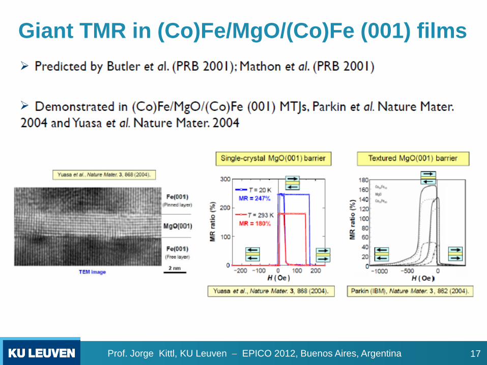
Giant TMR in (Co)Fe/MgO/(Co)Fe (001) films
17 Prof. Jorge Kittl, KU Leuven - EPICO 2012, Buenos Aires, Argentina

Giant TMR in FeCoB/MgO/FeCoB
polycrystalline films
18 Prof. Jorge Kittl, KU Leuven - EPICO 2012, Buenos Aires, Argentina

MRAM Building Block: The MTJ
19 Prof. Jorge Kittl, KU Leuven - EPICO 2012, Buenos Aires, Argentina
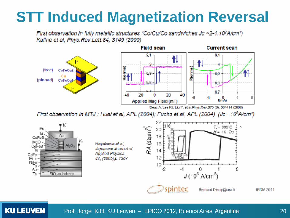
STT Induced Magnetization Reversal
20 Prof. Jorge Kittl, KU Leuven - EPICO 2012, Buenos Aires, Argentina

STT-MRAM Endurance
21 Prof. Jorge Kittl, KU Leuven - EPICO 2012, Buenos Aires, Argentina

Benchmarking - Memories
22 Prof. Jorge Kittl, KU Leuven - EPICO 2012, Buenos Aires, Argentina

STT - Possible Applications
23 Prof. Jorge Kittl, KU Leuven - EPICO 2012, Buenos Aires, Argentina

• Thermal Stability: DD= Energy/kT, E ~ V
• Write Current Density: Jc
• Stack Patterning• Stack Deposition
• TMR Ratio (Ion/Ioff)
• RA Variability
Technical Challenges
24 Prof. Jorge Kittl, KU Leuven - EPICO 2012, Buenos Aires, Argentina

Perpendicular vs. in-plane STT-RAM
25 Prof. Jorge Kittl, KU Leuven - EPICO 2012, Buenos Aires, Argentina

Retention (Thermal Stability)
26 Prof. Jorge Kittl, KU Leuven - EPICO 2012, Buenos Aires, Argentina
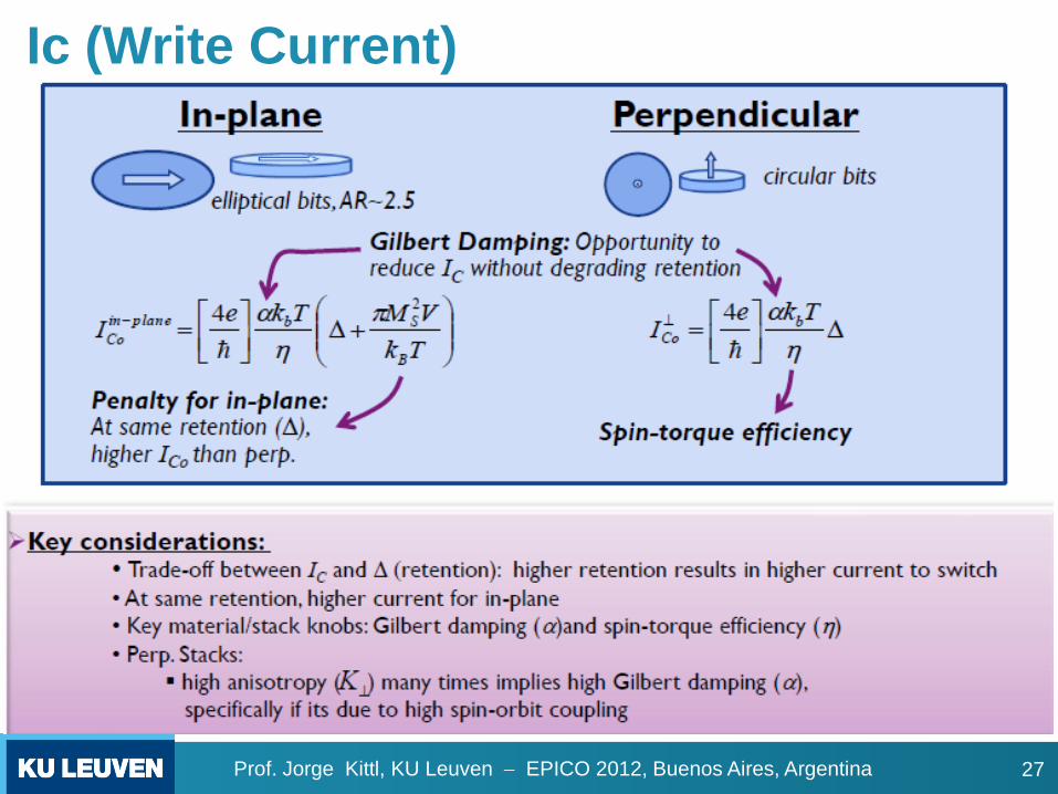
Ic (Write Current)
27 Prof. Jorge Kittl, KU Leuven - EPICO 2012, Buenos Aires, Argentina

Scaling Considerations
28 Prof. Jorge Kittl, KU Leuven - EPICO 2012, Buenos Aires, Argentina
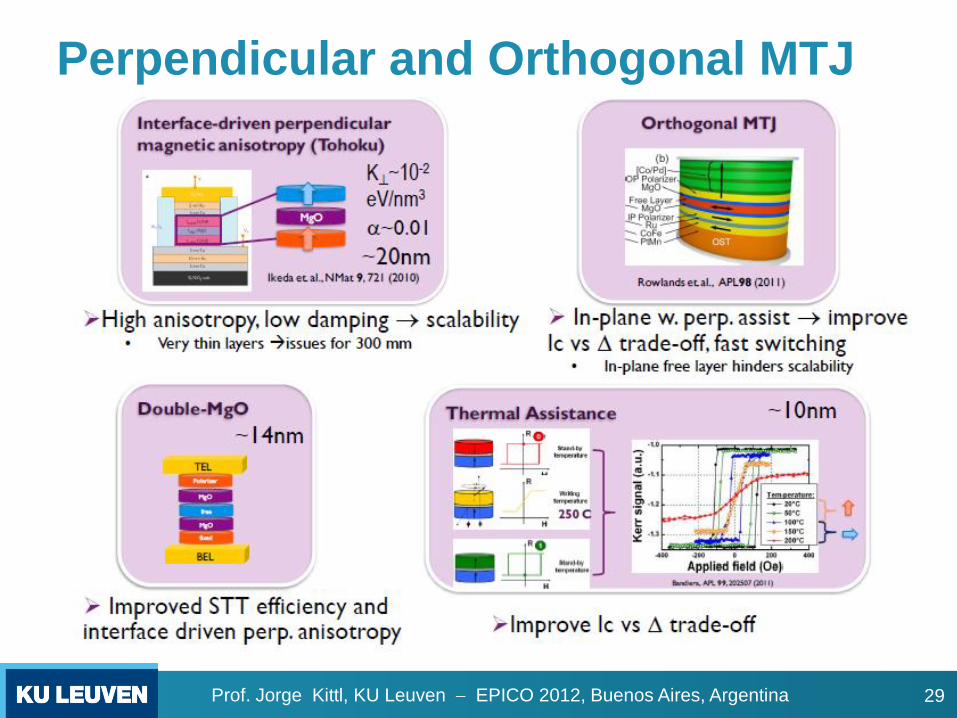
Perpendicular and Orthogonal MTJ
29 Prof. Jorge Kittl, KU Leuven - EPICO 2012, Buenos Aires, Argentina
Perpendicular STT-RAM Scalability
30 Prof. Jorge Kittl, KU Leuven - EPICO 2012, Buenos Aires, Argentina

Perpendicular STT-RAM Scalability
31 Prof. Jorge Kittl, KU Leuven - EPICO 2012, Buenos Aires, Argentina
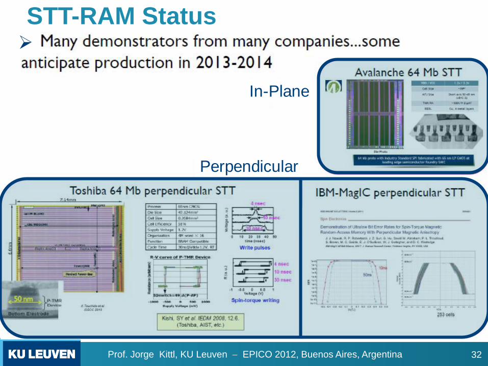
In-Plane
Perpendicular
STT-RAM Status
32 Prof. Jorge Kittl, KU Leuven - EPICO 2012, Buenos Aires, Argentina
Outline
Introduction
STT-RAM
RRAM Systems
o OXRAM
o CBRAM
o Mott
Summary
33 Prof. Jorge Kittl, KU Leuven - EPICO 2012, Buenos Aires, Argentina

Switching
element:
Reset: thermal disruption of conductive path
Set and reset: ionic transport in opposite directions (according to field polarity)
RRAM polarity
34 Prof. Jorge Kittl, KU Leuven - EPICO 2012, Buenos Aires, Argentina

Switching
element:
Reset: thermal disruption of conductive path
Set and reset: ionic transport in opposite directions (according to field polarity)
“gentler” “balanced”=> more reliable (e.g. higher endurance)
RRAM polarity
35 Prof. Jorge Kittl, KU Leuven - EPICO 2012, Buenos Aires, Argentina
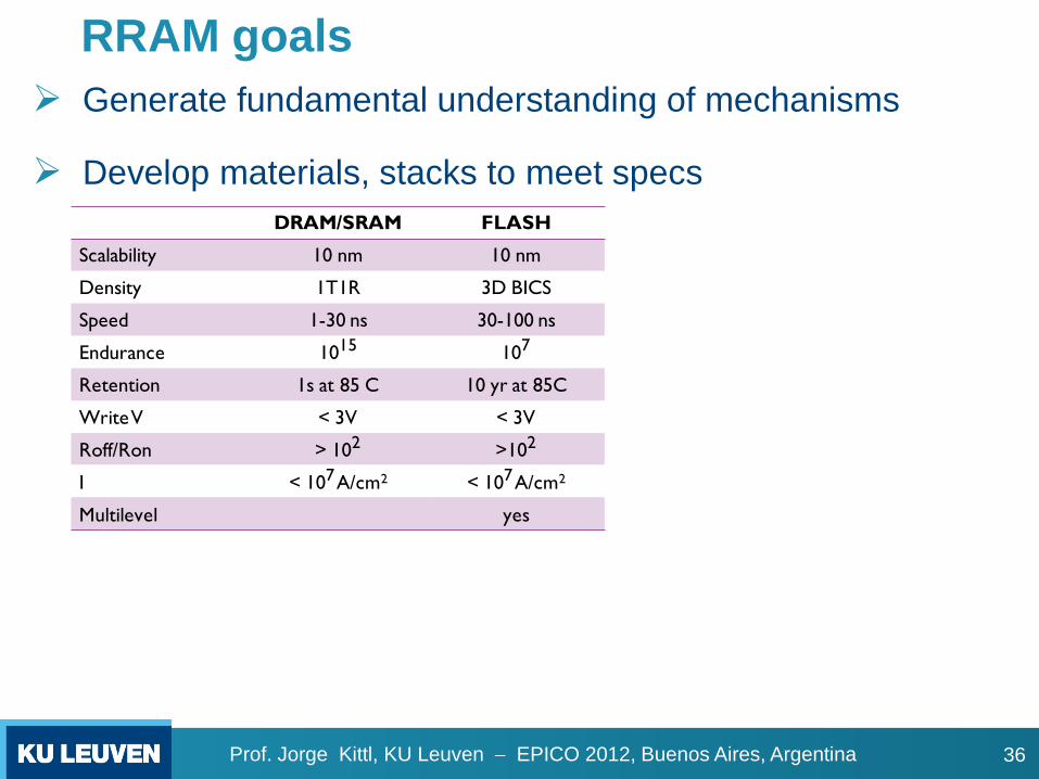
RRAM goals
Generate fundamental understanding of mechanisms
Develop materials, stacks to meet specs
DRAM/SRAM FLASH
Scalability 10 nm 10 nm
Density 1T1R 3D BICS
Speed 1-30 ns 30-100 ns
Endurance 1015 107
Retention 1s at 85 C 10 yr at 85C
WriteV < 3V < 3V
Roff/Ron > 102 >102
I < 107A/cm2 < 107A/cm2
Multilevel yes
36 Prof. Jorge Kittl, KU Leuven - EPICO 2012, Buenos Aires, Argentina

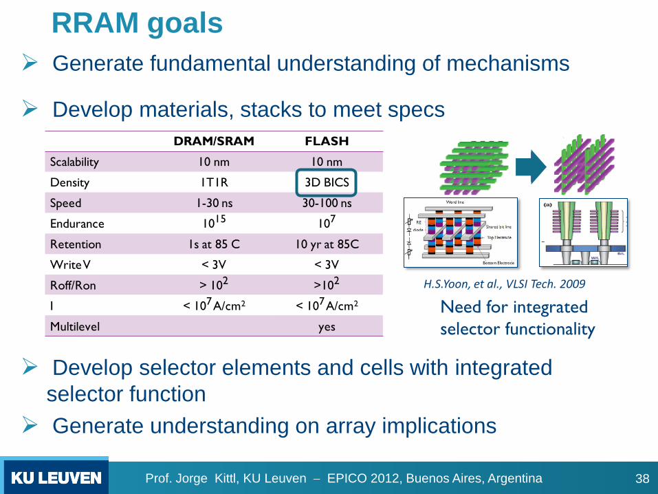
RRAM goals
Generate fundamental understanding of mechanisms
Develop materials, stacks to meet specs
DRAM/SRAM FLASH
Scalability 10 nm 10 nm
Density 1T1R 3D BICS
Speed 1-30 ns 30-100 ns
Endurance 1015 107
Retention 1s at 85 C 10 yr at 85C
WriteV < 3V < 3V
Roff/Ron > 102 >102
I < 107A/cm2 < 107A/cm2
Multilevel yes
H.S.Yoon, et al., VLSI Tech. 2009
Need for integrated
selector functionality
(prevent sneak currents)
37 Prof. Jorge Kittl, KU Leuven - EPICO 2012, Buenos Aires, Argentina
RRAM goals
Generate fundamental understanding of mechanisms
Develop materials, stacks to meet specs
Develop selector elements and cells with integrated
selector function
Generate understanding on array implications
DRAM/SRAM FLASH
Scalability 10 nm 10 nm
Density 1T1R 3D BICS
Speed 1-30 ns 30-100 ns
Endurance 1015 107
Retention 1s at 85 C 10 yr at 85C
WriteV < 3V < 3V
Roff/Ron > 102 >102
I < 107A/cm2 < 107A/cm2
Multilevel yes
H.S.Yoon, et al., VLSI Tech. 2009
Need for integrated
selector functionality
38 Prof. Jorge Kittl, KU Leuven - EPICO 2012, Buenos Aires, Argentina
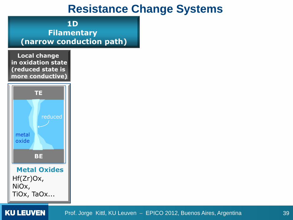
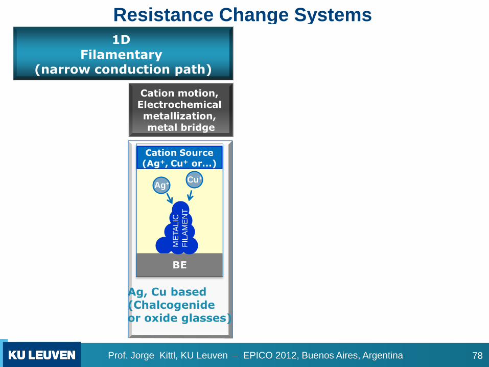
1D Filamentary
(narrow conduction path)
Local change in oxidation state (reduced state is more conductive)
Metal Oxides
TE
BE
metaloxide
reduced
Hf(Zr)Ox, NiOx, TiOx, TaOx...
Resistance Change Systems
39 Prof. Jorge Kittl, KU Leuven - EPICO 2012, Buenos Aires, Argentina
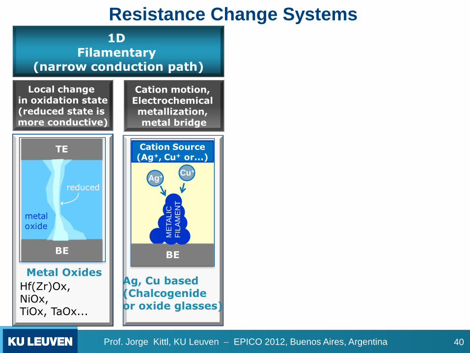
Cation motion, Electrochemical metallization, metal bridge
Ag, Cu based (Chalcogenide or oxide glasses)
Cation Source (Ag+, Cu+ or...)
Cu+
Ag+
BE
ME
TA
LIC
FIL
AM
EN
T
1D Filamentary
(narrow conduction path)
Local change in oxidation state (reduced state is more conductive)
Metal Oxides
TE
BE
metaloxide
reduced
Hf(Zr)Ox, NiOx, TiOx, TaOx...
Resistance Change Systems
40 Prof. Jorge Kittl, KU Leuven - EPICO 2012, Buenos Aires, Argentina
Cation motion, Electrochemical metallization, metal bridge
Ag, Cu based (Chalcogenide or oxide glasses)
Cation Source (Ag+, Cu+ or...)
Cu+
Ag+
BE
ME
TA
LIC
FIL
AM
EN
T
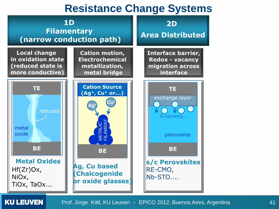
Interface barrier, Redox - vacancy
migration across interface
2D
Area Distributed
s/c Perovskites RE-CMO, Nb-STO....
TE
BE
exchange layer
O vacancy,...
perovskite
1D Filamentary
(narrow conduction path)
Local change in oxidation state (reduced state is more conductive)
Metal Oxides
TE
BE
metaloxide
reduced
Hf(Zr)Ox, NiOx, TiOx, TaOx...
Resistance Change Systems
41 Prof. Jorge Kittl, KU Leuven - EPICO 2012, Buenos Aires, Argentina
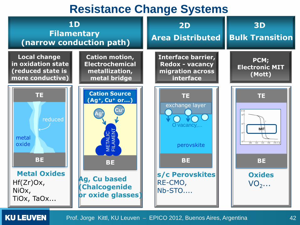
PCM; Electronic MIT
(Mott)
Cation motion, Electrochemical metallization, metal bridge
Ag, Cu based (Chalcogenide or oxide glasses)
Oxides
VO2...
3D
Bulk Transition
Cation Source (Ag+, Cu+ or...)
Cu+
Ag+
BE
ME
TA
LIC
FIL
AM
EN
T
Interface barrier, Redox - vacancy
migration across interface
2D
Area Distributed
s/c Perovskites RE-CMO, Nb-STO....
TE
BE
MITMIT
TE
BE
exchange layer
O vacancy,...
perovskite
1D Filamentary
(narrow conduction path)
Local change in oxidation state (reduced state is more conductive)
Metal Oxides
TE
BE
metaloxide
reduced
Hf(Zr)Ox, NiOx, TiOx, TaOx...
Resistance Change Systems
42 Prof. Jorge Kittl, KU Leuven - EPICO 2012, Buenos Aires, Argentina

PCM; Electronic MIT
(Mott)
Cation motion, Electrochemical metallization, metal bridge
Ag, Cu based (Chalcogenide or oxide glasses)
Oxides
VO2...
3D
Bulk Transition
Cation Source (Ag+, Cu+ or...)
Cu+
Ag+
BE
ME
TA
LIC
FIL
AM
EN
T
Interface barrier, Redox - vacancy
migration across interface
2D
Area Distributed
s/c Perovskites RE-CMO, Nb-STO....
TE
BE
MITMIT
TE
BE
exchange layer
O vacancy,...
perovskite
1D Filamentary
(narrow conduction path)
Local change in oxidation state (reduced state is more conductive)
Metal Oxides
TE
BE
metaloxide
reduced
Hf(Zr)Ox, NiOx, TiOx, TaOx...
Resistance Change Systems
43 Prof. Jorge Kittl, KU Leuven - EPICO 2012, Buenos Aires, Argentina
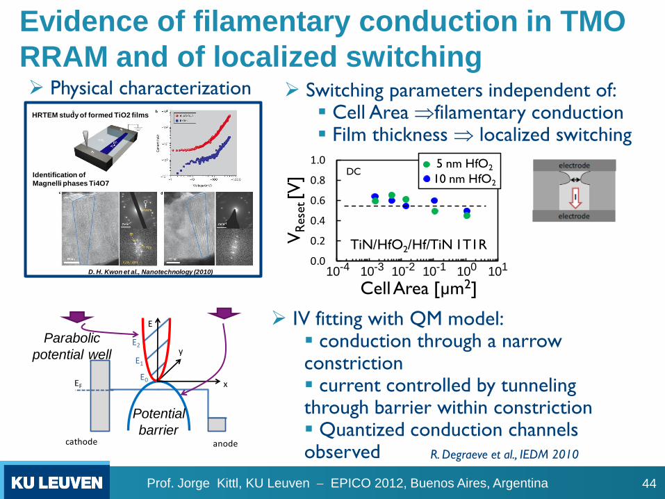
Evidence of filamentary conduction in TMO
RRAM and of localized switching Switching parameters independent of:
Cell Area filamentary conduction Film thickness localized switching
Physical characterization HRTEM study of formed TiO2 films
Identification of
Magnelli phases Ti4O7
D. H. Kwon et al., Nanotechnology (2010)
IV fitting with QM model: conduction through a narrow constriction current controlled by tunneling through barrier within constriction Quantized conduction channels observed
anode
E0
E1
E2
cathode
x
y
E
EF
Parabolic
potential well
Potential
barrier
0.0
0.2
0.4
0.6
0.8
1.0
1.00E-04 1.00E-03 1.00E-02 1.00E-01 1.00E+00 1.00E+0110-4 10-3 10-2 10-1 100 101
TiN/HfO2/Hf/TiN 1T1RVR
ese
t[V
] DC
Cell Area [µm2]
5 nm HfO2
10 nm HfO2
R. Degraeve et al., IEDM 2010
44 Prof. Jorge Kittl, KU Leuven - EPICO 2012, Buenos Aires, Argentina
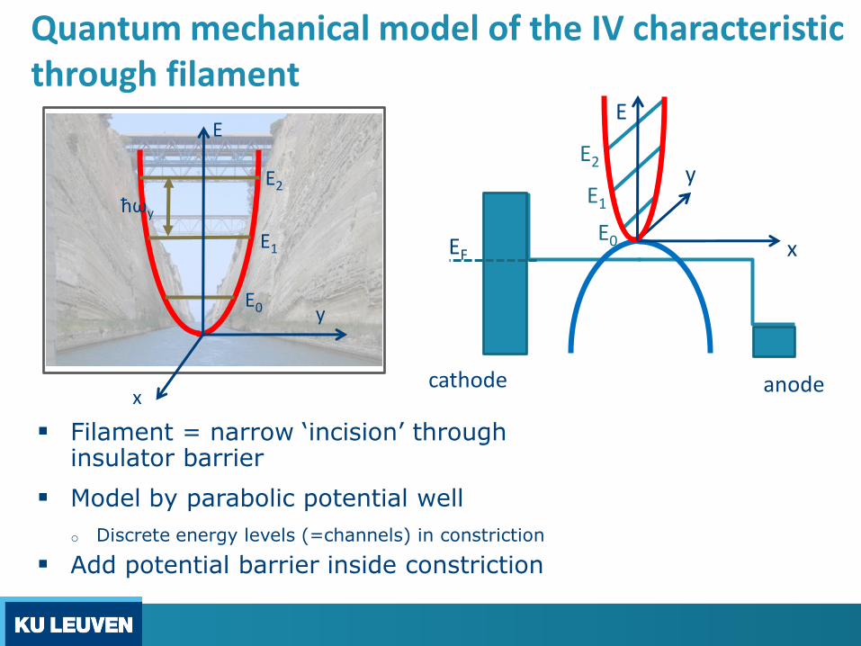
Filament = narrow ‘incision’ through insulator barrier
Model by parabolic potential well
o Discrete energy levels (=channels) in constriction
Add potential barrier inside constriction
ħωy
E0
E1
E2
x
y
E
anode
E0
E1
E2
cathode
x
y
E
EF
Quantum mechanical model of the IV characteristic through filament
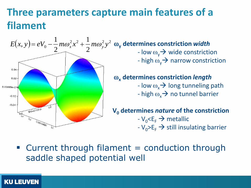
Three parameters capture main features of a filament
Current through filament = conduction through saddle shaped potential well
2222
02
1
2
1, ymxmeVyxE yx - y determines constriction width
- low y wide constriction - high y narrow constriction x determines constriction length - low x long tunneling path - high x no tunnel barrier V0 determines nature of the constriction - V0<EF metallic - V0>EF still insulating barrier

4-Channel Quantization at 25oC
R. Degraeve et al, VLSI-TSA 2012
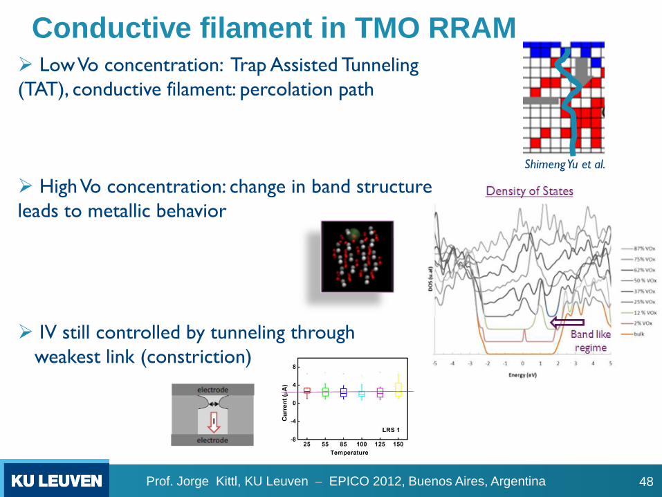
Conductive filament in TMO RRAM
Shimeng Yu et al.
Low Vo concentration: Trap Assisted Tunneling
(TAT), conductive filament: percolation path
High Vo concentration: change in band structure
leads to metallic behavior
IV still controlled by tunneling through
weakest link (constriction)
48 Prof. Jorge Kittl, KU Leuven - EPICO 2012, Buenos Aires, Argentina
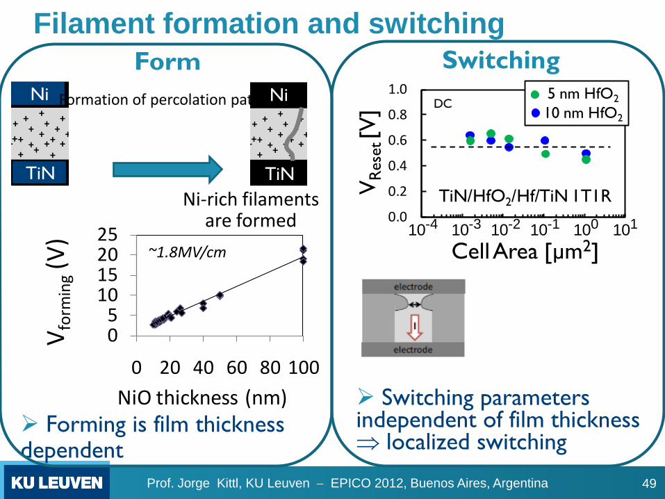
Filament formation and switching
05
10152025
0 20 40 60 80 100
Vfo
rmin
g(V
)
NiO thickness (nm)
~1.8MV/cm
+ +
+
++
++ ++
+
+ +
++
+++
++
++ +
++
+
+
Ni or Pt
TiN
Ni
TiN
Ni-rich filaments are formed
+ +
+
++
++ ++
+
+ +
++
+++
++
++ +
++
+
+
Ni or Pt
TiN
Ni
TiN
Formation of percolation path
Forming is film thickness dependent
Switching parameters independent of film thickness localized switching
0.0
0.2
0.4
0.6
0.8
1.0
1.00E-04 1.00E-03 1.00E-02 1.00E-01 1.00E+00 1.00E+0110-4 10-3 10-2 10-1 100 101
TiN/HfO2/Hf/TiN 1T1RVR
ese
t[V
] DC
Cell Area [µm2]
5 nm HfO2
10 nm HfO2
Form Switching
49 Prof. Jorge Kittl, KU Leuven - EPICO 2012, Buenos Aires, Argentina
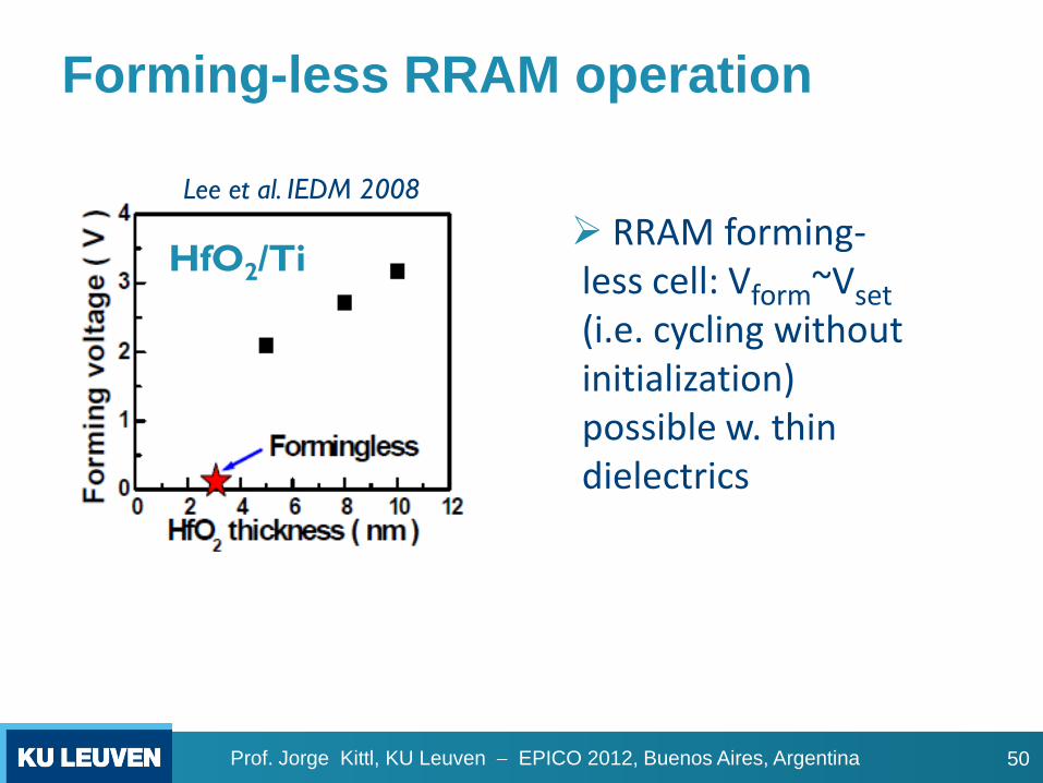
Forming-less RRAM operation
Lee et al. IEDM 2008
RRAM forming-less cell: Vform~Vset (i.e. cycling without initialization) possible w. thin dielectrics
HfO2/Ti
50 Prof. Jorge Kittl, KU Leuven - EPICO 2012, Buenos Aires, Argentina

Bipolar switching in HfO2/reactive metal system
RESET SET
ALD HfO2 10nm
PVD TiN 40nm
PVD TiN 30nm
PVD Hf 10nm
HfO2/Hf HfO2/Ti
Lee et. al, IEDM 2008
General trend: - Abrupt SET (runaway effect) - Gradual RESET (self-limiting)
51 Prof. Jorge Kittl, KU Leuven - EPICO 2012, Buenos Aires, Argentina

Capping Layer Role
Hf-Capping: Hf/O XPS Profiles
52 Prof. Jorge Kittl, KU Leuven - EPICO 2012, Buenos Aires, Argentina
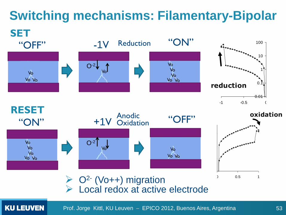
O2- (Vo++) migration Local redox at active electrode
Switching mechanisms: Filamentary-Bipolar
VoO-2
0.01
0.1
1
10
100
-1 -0.5 0 0.5 1
NiOreduction
Reduction
Vo Vo
Vo
VoVoVo
VoVo
-1V “OFF” “ON” SET
Anodic Oxidation
Vo Vo
Vo
VoVoVo
VoVo
0.01
0.1
1
10
100
-1 -0.5 0 0.5 1
O2- driftoxidation
VoO-2
+1V “ON” “OFF”
NiO
RESET
53 Prof. Jorge Kittl, KU Leuven - EPICO 2012, Buenos Aires, Argentina
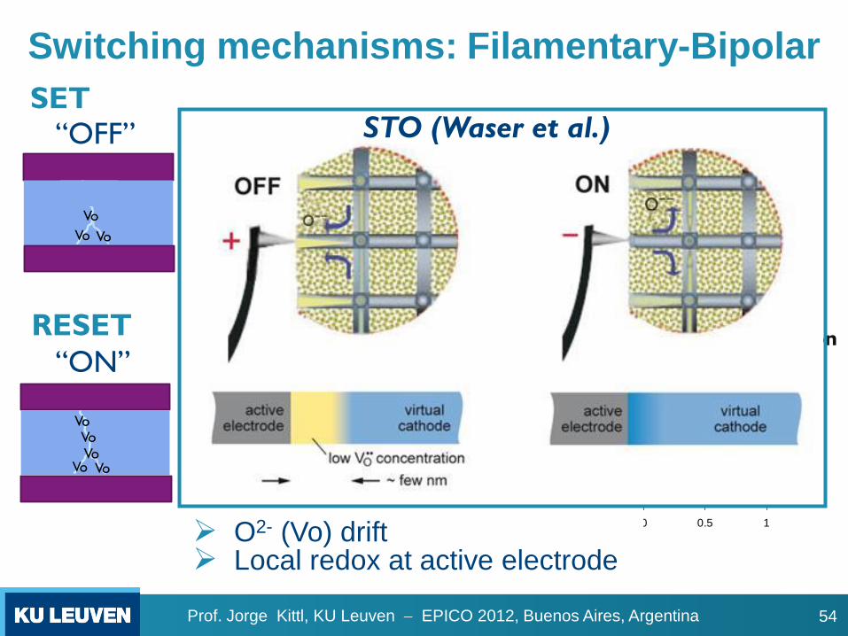
O2- (Vo) drift Local redox at active electrode
VoO-2
0.01
0.1
1
10
100
-1 -0.5 0 0.5 1
NiOreduction
Reduction
Vo Vo
Vo
VoVoVo
VoVo
-1V “OFF” “ON” SET
Anodic Oxidation
Vo Vo
Vo
VoVoVo
VoVo
0.01
0.1
1
10
100
-1 -0.5 0 0.5 1
O2- driftoxidation
VoO-2
+1V “ON” “OFF”
NiO
RESET
STO (Waser et al.)
Switching mechanisms: Filamentary-Bipolar
54 Prof. Jorge Kittl, KU Leuven - EPICO 2012, Buenos Aires, Argentina
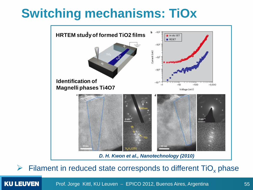
Switching mechanisms: TiOx
Filament in reduced state corresponds to different TiOx phase
HRTEM study of formed TiO2 films
Identification of
Magnelli phases Ti4O7
D. H. Kwon et al., Nanotechnology (2010)
55 Prof. Jorge Kittl, KU Leuven - EPICO 2012, Buenos Aires, Argentina
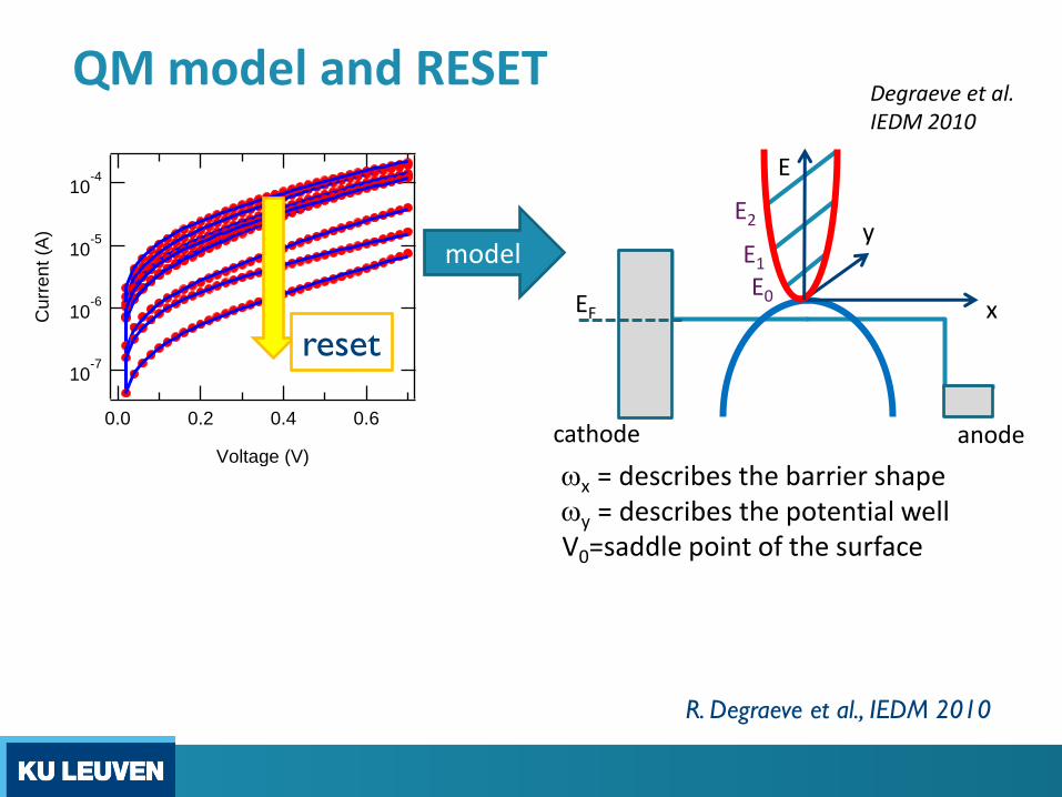
QM model and RESET
anode
E0
E1
E2
cathode
x
y
E
EF
x = describes the barrier shape y = describes the potential well V0=saddle point of the surface
Degraeve et al. IEDM 2010
10-7
10-6
10-5
10-4
Cu
rre
nt
(A)
0.60.40.20.0
Voltage (V)
reset
model
R. Degraeve et al., IEDM 2010
10-7
10-6
10-5
10-4
Cu
rre
nt
(A)
0.60.40.20.0
Voltage (V)
reset reset
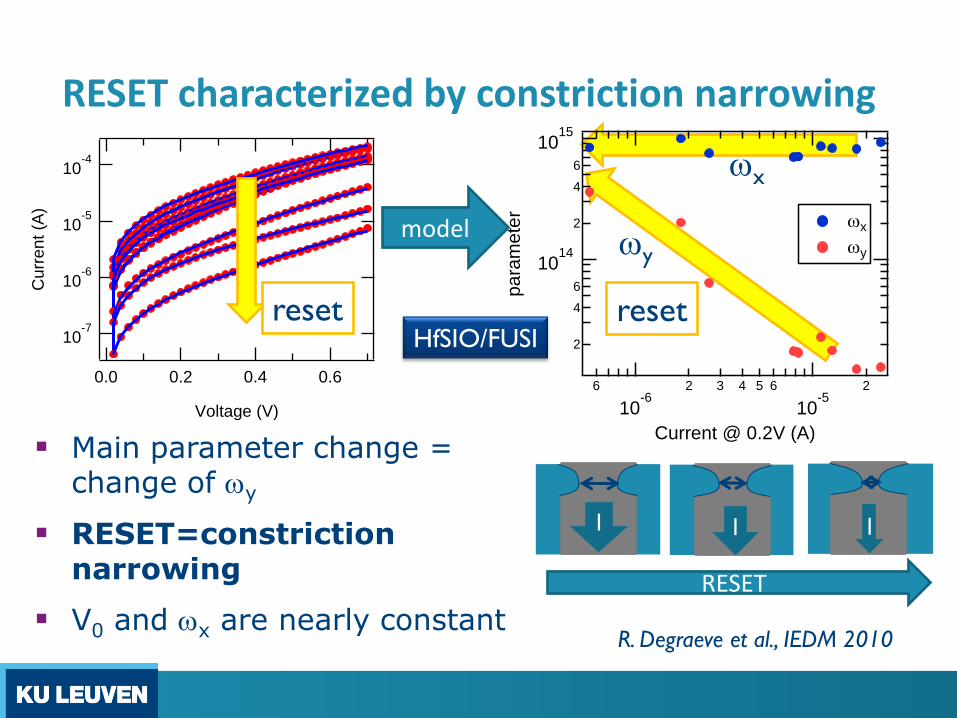
y
x
2
4
6
1014
2
4
6
1015
pa
ram
ete
r
6
10-6
2 3 4 5 6
10-5
2
Current @ 0.2V (A)
x
y
RESET characterized by constriction narrowing
Main parameter change = change of y
RESET=constriction narrowing
V0 and x are nearly constant
model
I I I
RESET
HfSIO/FUSI
R. Degraeve et al., IEDM 2010
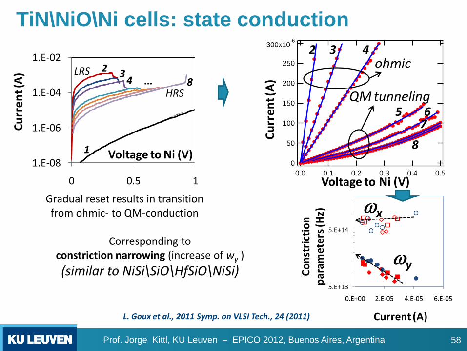
TiN\NiO\Ni cells: state conduction
1.E-08
1.E-06
1.E-04
1.E-02
0 0.5 1
LRS
HRS
1 Voltage to Ni (V)
Cu
rre
nt (
A) 2
83
4 ...
0
5
10
0 20 40
1.5MV/cm
tox (nm)
VF (V)
300x10-6
250
200
150
100
50
0
Curr
ent (A
)
0.50.40.30.20.10.0
Voltage (V)Voltage to Ni (V)
Cu
rre
nt (
A)
2 3 4
5 67
8
(c)ohmic
QM tunneling
5.E+13
5.E+14
0.E+00 2.E-05 4.E-05 6.E-05
x
y
Co
nst
rict
ion
p
aram
eter
s (H
z)Current (A)
(b)Gradual reset results in transition from ohmic- to QM-conduction
Corresponding to constriction narrowing (increase of wy )
(similar to NiSi\SiO\HfSiO\NiSi)
L. Goux et al., 2011 Symp. on VLSI Tech., 24 (2011)
58 Prof. Jorge Kittl, KU Leuven - EPICO 2012, Buenos Aires, Argentina

NiO cells: Influence of anode material
5.E+13
5.E+14
0.E+00 2.E-05 4.E-05 6.E-05
x
yC
on
stri
ctio
n
par
amet
ers
(Hz)
Current (A)
(b)
Reset constriction is controlled by appropriate anode material
Blue circles: Pt anode
red squares: Ni anode
NiO thickness = 40nm
300x10-6
250
200
150
100
50
0
Cu
rre
nt
(A)
0.80.60.40.20.0
Voltage (V)
TiN\NiO\Pt(a)
Voltage to Pt (V)
Cu
rre
nt (
A)Same results with catalytic Pt anode
(reset is not due to Ni injection)
5 channels Ei+1-Ei=80meV
L. Goux et al., 2011 Symp. on VLSI Tech., 24 (2011)
59 Prof. Jorge Kittl, KU Leuven - EPICO 2012, Buenos Aires, Argentina
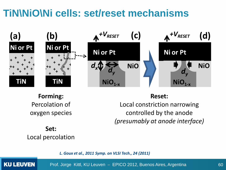
TiN\NiO\Ni cells: set/reset mechanisms
Forming: Percolation of oxygen species
+ +
+
++
++ ++
+
+ +
++
+++
++
++ +
++
+
+
Ni or Pt
TiN
+ +
+
++
++ ++
+
+ +
++
+++
++
++ +
++
+
+
Ni or Pt
TiN
(a) (b) (c)
dx
Ni or Pt
NiO1-x
NiOdy dy
Ni or Pt
NiO1-x
NiO
(d)+VRESET+VRESET
Reset: Local constriction narrowing
controlled by the anode (presumably at anode interface)
Set: Local percolation
L. Goux et al., 2011 Symp. on VLSI Tech., 24 (2011)
60 Prof. Jorge Kittl, KU Leuven - EPICO 2012, Buenos Aires, Argentina

Scaled TiN\NiO\Ni cells: anode engineering
Anode performances: Ni>Pt>NiPt>NiPtSi>TiN>TaN>Ti
stack Switching mode Ref.
Ni\NiO\Ni Non-polar
Pt\NiO\Pt Non-polar
Ni\NiO\TiN Unipolar
(Ni anode)
this
work
Pt\NiO\TiN Unipolar
(Pt anode)
TiN\NiO\TiN Super-linear LRS
NiPt\NiO\Ni Non-polar
NiPtSi\NiO\Ni Non-polar
Stack engineering: non-polar switching is
allowed provided both BE and TE have appropriate
catalytic properties
L. Goux et al., IEEE TED 56 (2009)
H. Akinaga et al., Proc. IEEE, 98 (2010); I.H. Inoue et al., Phys. Rev. B 77 (2008)
L. Goux et al., 2011 Symp. on VLSI Tech., 24 (2011)
61 Prof. Jorge Kittl, KU Leuven - EPICO 2012, Buenos Aires, Argentina

Scaled TiN\NiO\Ni cells: TEM/EELS
Pile-up of oxygen at the NiO\Ni interface after
reset switching
20 nm20 nm20 nm20 nm20 nm
TiN
NiONiTiN
PMD
~80nm
2
1
1.E+03
1.E+04
1.E+05
1 10 100
Voltage to Ni (V)
# switching cycles
Cu
rre
nt
(A)
HRS
LRS78.5
96.5
Ni
TiNNiO
NiONi
TiN
Ni
TiNNiO (a)
(b)
(e)
(c)
Re
sist
ance
(
)
0.E+00
5.E-05
1.E-04
0 0.5 1
10
100
1000
10 100 1000
ICOMP (A)
IRESET (A)(d)
0.E+00
3.E+06
5.E+06
0.E+00 4.E-08 8.E-08
0.E+00
5.E+05
1.E+06
0.E+00 4.E-08 8.E-08
0.E+00
1.E+05
2.E+05
3.E+05
0.E+00 4.E-08 8.E-08
TiNNiNiOTiN
1 2
Co
un
ts (T
i)C
ou
nts
(O)
Position (nm)
Co
un
ts (N
i)before reset
0.E+00
3.E+06
5.E+06
0.E+00 4.E-08 8.E-08
0.E+00
5.E+05
1.E+06
0.E+00 4.E-08 8.E-08
0.E+00
1.E+05
2.E+05
3.E+05
0.E+00 4.E-08 8.E-08
TiNNiNiOTiN
1 2
Co
un
ts (T
i)C
ou
nts
(O)
Position (nm)
Co
un
ts (N
i)after reset
L. Goux et al., 2011 Symp. on VLSI Tech., 24 (2011)
62 Prof. Jorge Kittl, KU Leuven - EPICO 2012, Buenos Aires, Argentina

Scalability of filament formation: filament formation depends
on local defects
Predictable area scaling for uniform distribution of defects (e.g.
amorphous material)
In crystalline material: grain size vs. cell size
Scalability of switching:
Good scalability (not much changes) expected down to scale of
filament (few nm)
Scalability to 10 nm!
Planarized BE
Implications of filamentary conduction, localized switching
HfO2-based 1T1R Govoreanu et al., IEDM 2011
63 Prof. Jorge Kittl, KU Leuven - EPICO 2012, Buenos Aires, Argentina
10 nm RRAM Cell
Govoreanu et al., IEDM 2011
64 Prof. Jorge Kittl, KU Leuven - EPICO 2012, Buenos Aires, Argentina

Variability:
Filament formed at defects...local atomic
configuration at constriction varies among filaments
(and for same filament with switching!)
Few atomic jumps may impact conduction of
narrow filament
Stochastic component (small numbers)
(however: “small number” stochastic variability
likely present for ANY technology when scaling
to nm range)
3000 /s
experiment
log(time)50x10-6
40
30
20
10
0
Cu
rre
nt (A
)
1.00.80.60.40.20.0
Voltage (V)
reset
0.0 0.2 0.4 0.6
Voltage (V)
Cu
rre
nt (
A
)
50
40
30
20
10
0
Implications of filamentary conduction, localized switching
65 Prof. Jorge Kittl, KU Leuven - EPICO 2012, Buenos Aires, Argentina

Retention: Few atomic jumps may impact conduction of narrow filament
variability of retention
Stronger (more conductive) filaments have better retention
Shimeng Yu, Y. Y. Chen, X. Guan, H.-S. Philip Wong, J. A. Kittl , Appl. Phys. Lett. 100, 043507 (2012)
MC simulations:
Implications of filamentary conduction, localized switching
66 Prof. Jorge Kittl, KU Leuven - EPICO 2012, Buenos Aires, Argentina

Switching voltage-pulse width trade-off
-9 -8 -7 -6 -50
0.2
0.4
0.6
0.8
1
Pulse duration, log(tp[s])
RE
set
vol
tage
, VR
E,S
et [V
]
T = 25C
0.5
1.0
1.5
2.0
2.5
1.00E-09 1.00E-08 1.00E-07 1.00E-06 1.00E-0510-9 10-8 10-7 10-6 10-5
Pulse Width [s]
Sw
itch V
oltage [V
]
Reset
Set
TiO2/Al2O3 Hf/HfO2
Shimeng Yu, Yi Wu, and H.-S. Philip Wong APL 98, 103514 (2011)
Exponential dependence of switching time on voltage
High speed (< 1 ns), low voltage switching achieved
67 Prof. Jorge Kittl, KU Leuven - EPICO 2012, Buenos Aires, Argentina

Retention and endurance in HfO2-based RRAM
Retention: LRS failure thermally activated
Stronger (wider) filaments
better retention
10 yr at 85C spec
Ea consistent with ab-initio +
molecular dynamic simulations of
diffusion
107
106
105
104
1031E+3
1E+4
1E+5
1E+6
1E+7
1E+0 1E+1 1E+2 1E+3 1E+4 1E+5 1E+6 1E+7 1E+8 1E+9100 101 102 103 104 105 106 107 108 109
R (
ohm
)
Cycle #
Rete
ntion T
ime (
s)
1/kT
Endurance: 1010 cycles achieved
68 Prof. Jorge Kittl, KU Leuven - EPICO 2012, Buenos Aires, Argentina
Retention and endurance in HfO2-based RRAM
Retention: LRS failure thermally activated
Stronger (wider) filaments
better retention
10 yr at 85C spec
Ea consistent with ab-initio +
molecular dynamic simulations of
diffusion
Rete
ntion T
ime (
s)
1/kT
Endurance: 1010 cycles achieved
69 Prof. Jorge Kittl, KU Leuven - EPICO 2012, Buenos Aires, Argentina
IEEE Trans on Electron Dev. 59, 3243 (2012)
Endurance and balanced cycling
Prof. Jorge Kittl, KU Leuven - EPICO 2012, Buenos Aires, Argentina 70
Too strong Reset: LRS failure Too strong Set: HRS failure
IEEE Trans on Electron Dev. 59, 3243 (2012)
Improving cycling: Stack optimization (HfO2-based 1T1R)
1.E-091.E-081.E-071.E-061.E-051.E-04
-1.6 -1.2 -0.8 -0.4 0-1.6 -1.2 -0.8 -0.4 0
Voltage (V)
Cu
rre
nt (A
)
10-4
10-5
10-6
10-7
10-8
10-9 1.E-091.E-081.E-071.E-061.E-051.E-04
-1.6 -1.2 -0.8 -0.4 0-1.6 -1.2 -0.8 -0.4 0
Voltage (V)
Cu
rre
nt (A
)
10-4
10-5
10-6
10-7
10-8
10-9
Switching with:
Lower variability
Lower current
Larger R window
Standard stack Optimized stack
71 Prof. Jorge Kittl, KU Leuven - EPICO 2012, Buenos Aires, Argentina
L. Goux et al, VLSI 2012
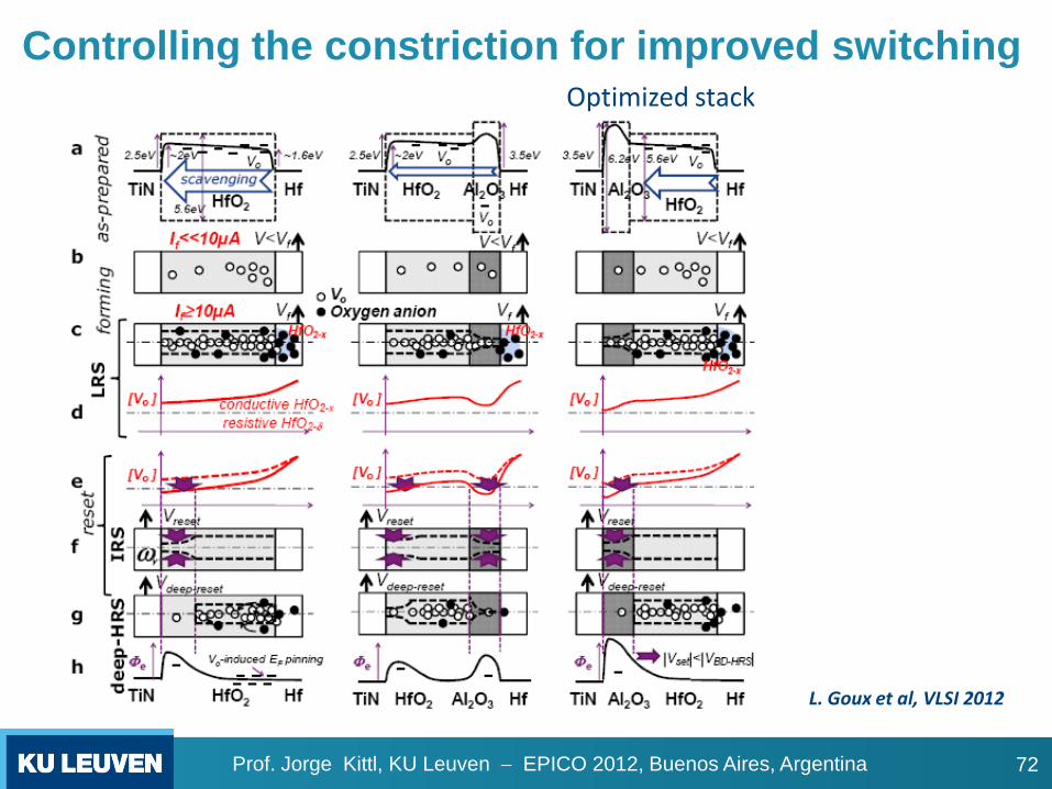
Controlling the constriction for improved switching
Prof. Jorge Kittl, KU Leuven - EPICO 2012, Buenos Aires, Argentina 72
Optimized stack
L. Goux et al, VLSI 2012
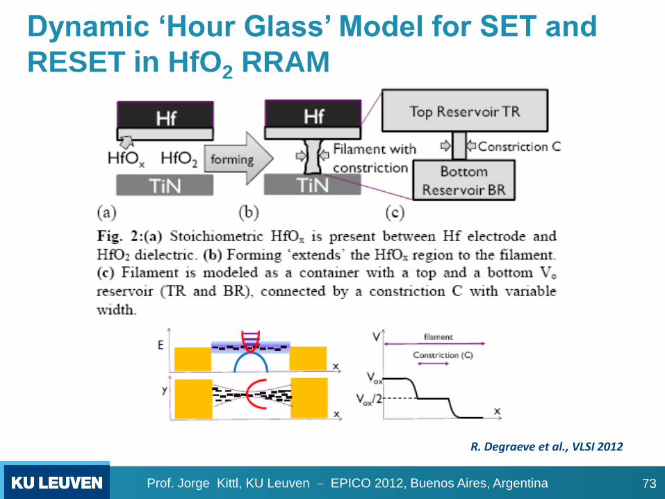
Dynamic ‘Hour Glass’ Model for SET and
RESET in HfO2 RRAM
Prof. Jorge Kittl, KU Leuven - EPICO 2012, Buenos Aires, Argentina 73
R. Degraeve et al., VLSI 2012

Dynamic ‘Hour Glass’ Model for SET and
RESET in HfO2 RRAM
Prof. Jorge Kittl, KU Leuven - EPICO 2012, Buenos Aires, Argentina 74
R. Degraeve et al., VLSI 2012
Dynamic ‘Hour Glass’ Model for SET and
RESET in HfO2 RRAM
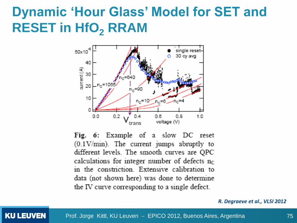
Prof. Jorge Kittl, KU Leuven - EPICO 2012, Buenos Aires, Argentina 75
R. Degraeve et al., VLSI 2012

Dynamic ‘Hour Glass’ Model for SET and
RESET in HfO2 RRAM
Prof. Jorge Kittl, KU Leuven - EPICO 2012, Buenos Aires, Argentina 76
R. Degraeve et al., VLSI 2012
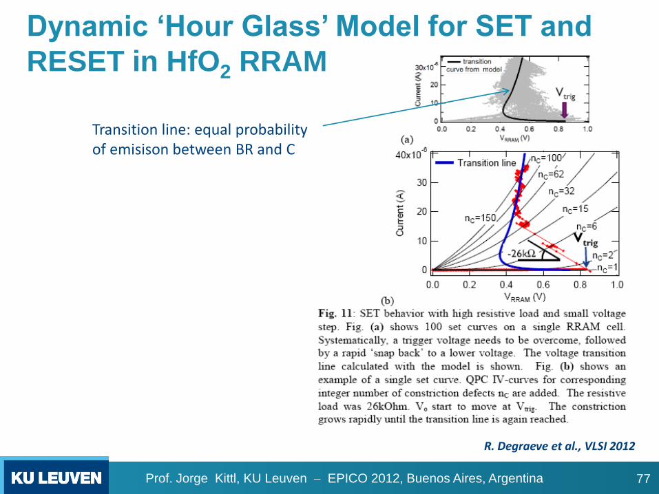
Prof. Jorge Kittl, KU Leuven - EPICO 2012, Buenos Aires, Argentina 77
R. Degraeve et al., VLSI 2012
Dynamic ‘Hour Glass’ Model for SET and
RESET in HfO2 RRAM
Transition line: equal probability of emisison between BR and C
PCM; Electronic MIT
(Mott)
Cation motion, Electrochemical metallization, metal bridge
Ag, Cu based (Chalcogenide or oxide glasses)
Oxides
VO2...
3D
Bulk Transition
Cation Source (Ag+, Cu+ or...)
Cu+
Ag+
BE
ME
TA
LIC
FIL
AM
EN
T
Interface barrier, Redox - vacancy
migration across interface
2D
Area Distributed
s/c Perovskites RE-CMO, Nb-STO....
TE
BE
MITMIT
TE
BE
exchange layer
O vacancy,...
perovskite
1D Filamentary
(narrow conduction path)
Local change in oxidation state (reduced state is more conductive)
Metal Oxides
TE
BE
metaloxide
reduced
Hf(Zr)Ox, NiOx, TiOx, TaOx...
Resistance Change Systems
78 Prof. Jorge Kittl, KU Leuven - EPICO 2012, Buenos Aires, Argentina

Operation
ON-switching:
Reduction @ cathode
Ag filament formation
Ag+ + e‘ Ag
OFF-switching:
Oxidation @ anode
Ag Ag+ + e‘
M. Faraday (1834)
Electrolyte
* amorphous GeSe2+x
and GeS2+x
* Disordered and amorphous
sulfides and oxides C. Schindler et al., IEEE T-ED, 54 (2007) 2762
CBRAM BASICS
79 Prof. Jorge Kittl, KU Leuven -
EPICO 2012, Buenos Aires,
Argentina
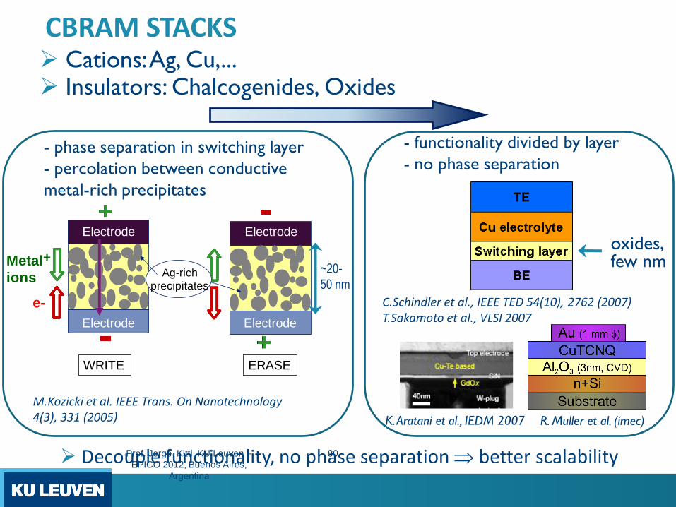
CBRAM STACKS Cations: Ag, Cu,... Insulators: Chalcogenides, Oxides
Decouple functionality, no phase separation better scalability
WRITE ERASE
Metal+
ions
e-
Ag-rich
precipitates
ElectrodeElectrode
ElectrodeElectrode
~20-
50 nm
K. Aratani et al., IEDM 2007 R. Muller et al. (imec)
oxides, few nm
M.Kozicki et al. IEEE Trans. On Nanotechnology 4(3), 331 (2005)
C.Schindler et al., IEEE TED 54(10), 2762 (2007) T.Sakamoto et al., VLSI 2007
- phase separation in switching layer
- percolation between conductive
metal-rich precipitates
- functionality divided by layer
- no phase separation
80 Prof. Jorge Kittl, KU Leuven -
EPICO 2012, Buenos Aires,
Argentina

Cu-BASED CBRAM UNDER STUDY
TECu-sourceCu+
Cu+
Cu+
Cu+
BE
Cell concept: engineered stack, separating functions by layers:
Cu-source and stack optimization
Combinatorial approach (e.g. Cu-Te composition)
A
B
AxBy
JORGE KITTL @ IMEC 2010 67
5
15
25
35
45
55
65
Te/(
Te+
Cu
)
Composition Cu-Te (XRF)
10 30 50 70
2theta
Crystallinity (XRD)
Cu
Cu
2Te
a
-Cu
Te
+ a
-Te
Cu-Te gradient
Cu
Te
IMEC partner conf idential – as listed in access slide
Mapping capabilities for composition, crystallinity, phase…
81 Prof. Jorge Kittl, KU Leuven -
EPICO 2012, Buenos Aires,
Argentina
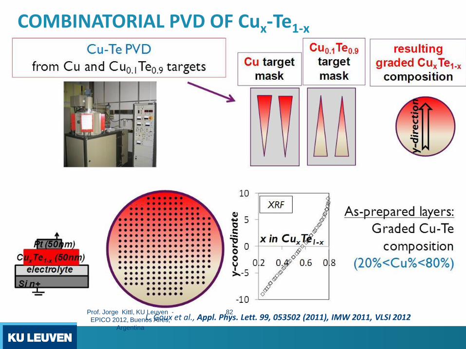
L. Goux et al., Appl. Phys. Lett. 99, 053502 (2011), IMW 2011, VLSI 2012
COMBINATORIAL PVD OF Cux-Te1-x
82 Prof. Jorge Kittl, KU Leuven -
EPICO 2012, Buenos Aires,
Argentina
7.5
8
8.5
0
2
4
0.2 0.3 0.4 0.5 0.6 0.7 0.8
Cell resista
nce
[Log(Ω)]
VFO
RM
ING (
V)
x in CuxTe1-x 1.E-12
1.E-08
1.E-04
0 2.5 5
x>0.7
Voltage (V)
Curr
ent
(A)
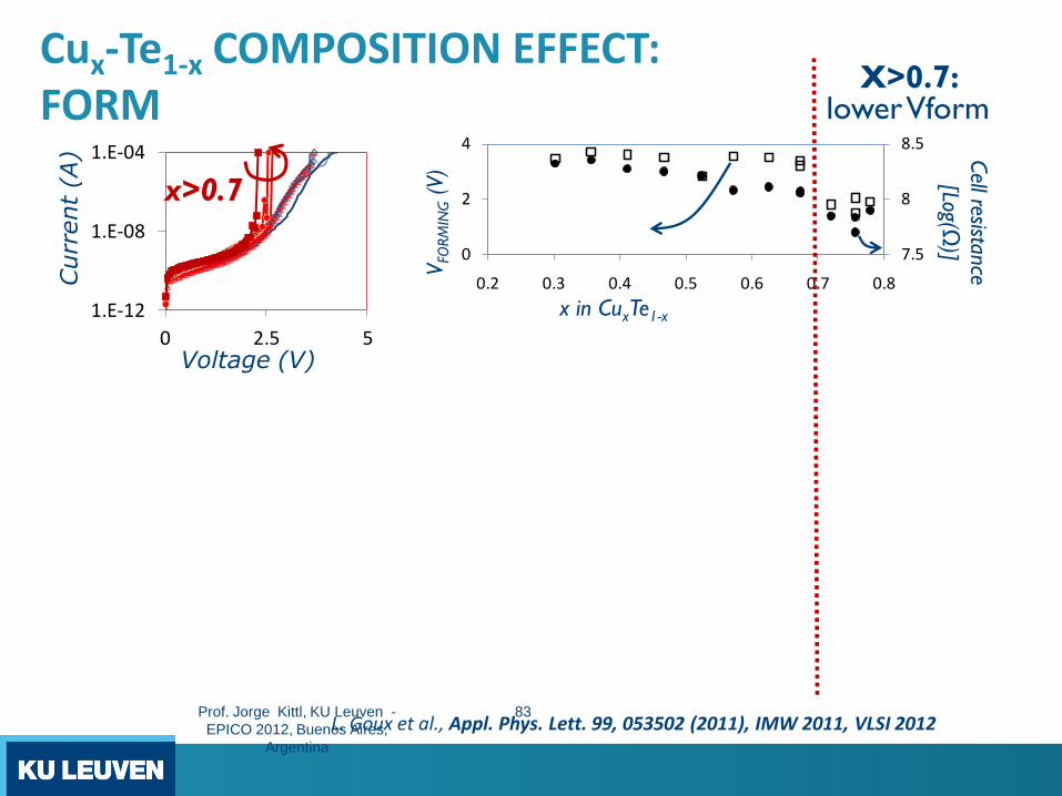
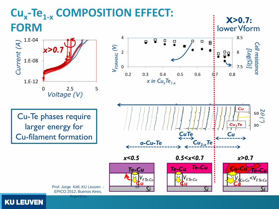
Cux-Te1-x COMPOSITION EFFECT: FORM
X>0.7: lower Vform
L. Goux et al., Appl. Phys. Lett. 99, 053502 (2011), IMW 2011, VLSI 2012 83 Prof. Jorge Kittl, KU Leuven -
EPICO 2012, Buenos Aires,
Argentina
7.5
8
8.5
0
2
4
0.2 0.3 0.4 0.5 0.6 0.7 0.8
Cell resista
nce
[Log(Ω)]
VFO
RM
ING (
V)
x in CuxTe1-x
x in CuxTe1-x
Form
ing
volt
age
(V)
Cell resistance (Ω
)
1030
5070
Intensity
2theta
Crys
tallin
ity(X
RD)
April
2010
1020304050607080
Te/(Te+Cu)
Comp
ositi
on
(XRF
) 30
50
Cu
Cu2Te
2()
Intensity (a.u.)
Cu2Te + CuCu2TeTe + CuTe
(a)
(b)
(c)
x=0.74x=0.67x=0.6x=0.35
amorphous Cu2Te-Crystal Cu inclusions
0.0E+00
5.0E+07
1.0E+08
1.5E+08
2.0E+08
2.5E+08
0
1
2
3
4
0.2 0.3 0.4 0.5 0.6 0.7 0.8
Forming voltageresistance
1.E-12
1.E-08
1.E-04
0 2.5 5
x>0.7
V(V)
I(A)
1030
5070
Intensity
2theta
Crys
tallin
ity(X
RD)
April
2010
1020304050607080
Te/(Te+Cu)
Comp
ositi
on
(XRF
) 30
50
Cu
Cu2Te
2()
Intensity (a.u.)
Cu2Te + CuCu2TeTe + CuTe
a-Cu-Te Cu2-xTe
Cu CuTe
2 ()
Si Si Si
x<0.5 0.5<x<0.7 x>0.7
Cu-Cu Te-Cu
VF.Cu-Cu<VF.Te-Cu
Te-CuTe-Cu
VF.Te-Cu
Te-Cu
VF.Te-CuCu Cu Cu
Cu-Te phases require
larger energy for
Cu-filament formation
1.E-12
1.E-08
1.E-04
0 2.5 5
x>0.7
Voltage (V)
Curr
ent
(A)
Cux-Te1-x COMPOSITION EFFECT: FORM
X>0.7: lower Vform
84 Prof. Jorge Kittl, KU Leuven -
EPICO 2012, Buenos Aires,
Argentina
x in CuxTe1-x
Form
ing
volt
age
(V)
Cell resistance (Ω
)
1030
5070
Intensity
2theta
Crys
tallin
ity(X
RD)
April
2010
1020304050607080
Te/(Te+Cu)
Comp
ositi
on
(XRF
) 30
50
Cu
Cu2Te
2()
Intensity (a.u.)
Cu2Te + CuCu2TeTe + CuTe
(a)
(b)
(c)
x=0.74x=0.67x=0.6x=0.35
amorphous Cu2Te-Crystal Cu inclusions
0.0E+00
5.0E+07
1.0E+08
1.5E+08
2.0E+08
2.5E+08
0
1
2
3
4
0.2 0.3 0.4 0.5 0.6 0.7 0.8
Forming voltageresistance
1.E-12
1.E-08
1.E-04
0 2.5 5
x>0.7
V(V)
I(A)
1030
5070
Intensity
2theta
Crys
tallin
ity(X
RD)
April
2010
1020304050607080
Te/(Te+Cu)
Comp
ositi
on
(XRF
) 30
50
Cu
Cu2Te
2()
Intensity (a.u.)
Cu2Te + CuCu2TeTe + CuTe
Cu2-xTe
Cu CuTe
2 ()
Si Si Si
x<0.5 0.5<x<0.7 x>0.7
Cu-Cu Te-Cu
VF.Cu-Cu<VF.Te-Cu
Te-CuTe-Cu
VF.Te-Cu
Te-Cu
VF.Te-CuCu Cu Cu
-10
-8
-6
-4
-2 -1 0 1 2 3
-10
-8
-6
-4
-2
-3 -2 -1 0 1 2
-10
-8
-6
-4
-2
-4 -2 0 2 4
(1) x=0.25
Curr
ent [L
og(A
)]Voltage to the Pt TE (V)
(2) x=0.57 (3) x=0.78
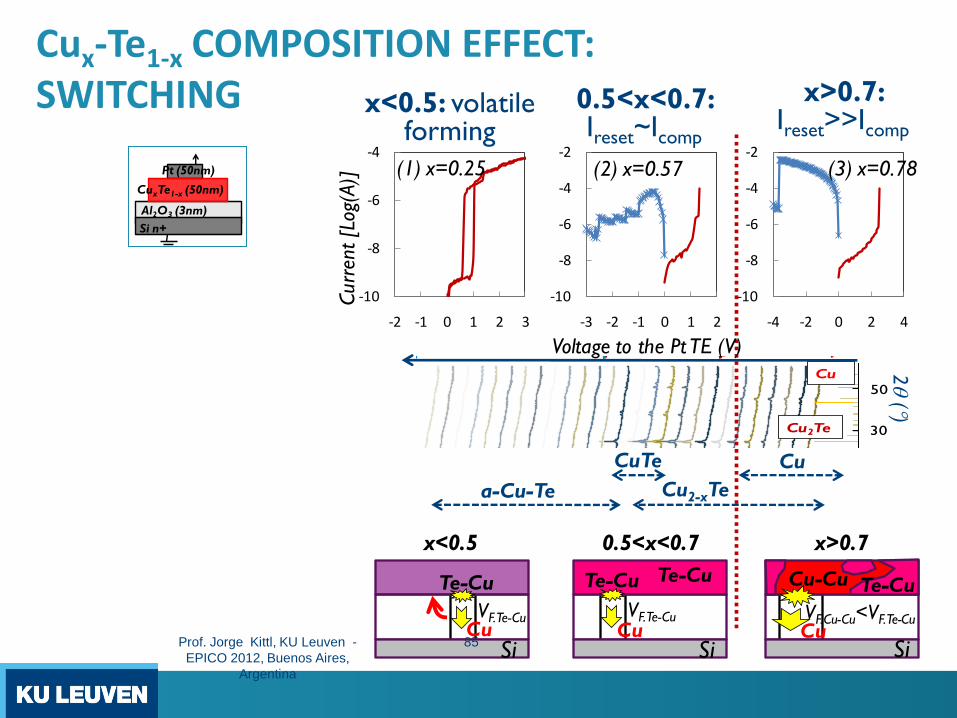
a-Cu-Te
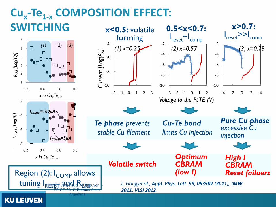
Cux-Te1-x COMPOSITION EFFECT: SWITCHING x<0.5: volatile
forming 0.5<x<0.7: Ireset~Icomp
x>0.7: Ireset>>Icomp
Si n+
Al2O3 (3nm)
Pt (50nm)
CuxTe1-x (50nm)
85 Prof. Jorge Kittl, KU Leuven -
EPICO 2012, Buenos Aires,
Argentina
-10
-8
-6
-4
-2 -1 0 1 2 3
-10
-8
-6
-4
-2
-3 -2 -1 0 1 2
-10
-8
-6
-4
-2
-4 -2 0 2 4
3
4
5
6
7
8
0.2 0.4 0.6 0.8
-8
-6
-4
-2
0.2 0.4 0.6 0.8
x in CuxTe1-x
ICOMP=5A
ICOMP=100A
x in CuxTe1-x
(3)(2)(1)
RLR
S[L
og(
)]
I RESE
T[L
og(A
)]
(1) x=0.25
Curr
ent [L
og(A
)]
Voltage to the Pt TE (V)
(2) x=0.57 (3) x=0.78
Region (2): ICOMP allows
tuning IRESET and RLRS
Cu-Te bond
limits Cu injection
Te phase prevents
stable Cu filament
Volatile switch Optimum CBRAM (low I)
-10
-8
-6
-4
-2 -1 0 1 2 3
-10
-8
-6
-4
-2
-3 -2 -1 0 1 2
-10
-8
-6
-4
-2
-4 -2 0 2 4
3
4
5
6
7
8
0.2 0.4 0.6 0.8
-8
-6
-4
-2
0.2 0.4 0.6 0.8
x in CuxTe1-x
ICOMP=5A
ICOMP=100A
x in CuxTe1-x
(3)(2)(1)
RLR
S[L
og(
)]
I RESE
T[L
og(A
)]
(1) x=0.25
Curr
ent [L
og(A
)]
Voltage to the Pt TE (V)
(2) x=0.57 (3) x=0.78
Pure Cu phase excessive Cu injection
High I CBRAM Reset failuers
Cux-Te1-x COMPOSITION EFFECT: SWITCHING
-10
-8
-6
-4
-2 -1 0 1 2 3
-10
-8
-6
-4
-2
-3 -2 -1 0 1 2
-10
-8
-6
-4
-2
-4 -2 0 2 4
(1) x=0.25
Curr
ent [L
og(A
)]Voltage to the Pt TE (V)
(2) x=0.57 (3) x=0.78
x<0.5: volatile forming
0.5<x<0.7: Ireset~Icomp
x>0.7: Ireset>>Icomp
L. Goux et al., Appl. Phys. Lett. 99, 053502 (2011), IMW 2011, VLSI 2012
86 Prof. Jorge Kittl, KU Leuven -
EPICO 2012, Buenos Aires,
Argentina
1.E+03
1.E+05
1.E+07
1.E+09
0 1000 2000 3000 4000 5000
resistan
ce at 0.1V
(ohm)
# cycles
LRS
HRS
109
107
105
103
Resi
stan
ce a
t 0.1
V (ohm
)
# cycles
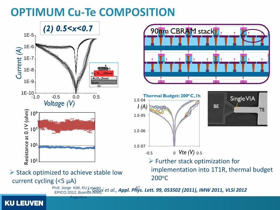
90nm CBRAM stack
1.E-07
1.E-06
1.E-05
1.E-04
-0.5 0 0.5
I (A)
Vte (V)
Thermal Budget: 200C,1h
Stack optimized to achieve stable low current cycling (<5 µA)
Further stack optimization for implementation into 1T1R, thermal budget 200oC
OPTIMUM Cu-Te COMPOSITION
Voltage (V)
Curr
ent (A
) (2) 0.5<x<0.7
-1.0 -0.5 0.0 0.51E-10
1E-9
1E-8
1E-7
1E-6
1E-5
Si n+
Al2O3 (3nm)
Pt (50nm)
CuxTe1-x (50nm)
L. Goux et al., Appl. Phys. Lett. 99, 053502 (2011), IMW 2011, VLSI 2012 87 Prof. Jorge Kittl, KU Leuven -
EPICO 2012, Buenos Aires,
Argentina
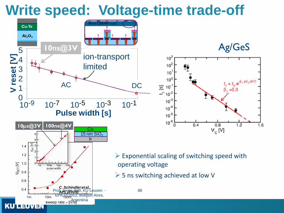
Write speed: Voltage-time trade-off 90nm CBRAM stack
0
1
2
3
4
5
1.E-09 1.E-07 1.E-05 1.E-03 1.E-01
PW (sec)
Vre
set(V
)
drift-limited switching
0
1
2
3
4
5
1.E-09 1.E-07 1.E-05 1.E-03 1.E-01
0
1
2
3
4
5
1.E-09 1.E-07 1.E-05 1.E-03 1.E-01
0
1
2
3
4
5
1.E-09 1.E-07 1.E-05 1.E-03 1.E-01
0
1
2
3
4
5
1.E-09 1.E-07 1.E-05 1.E-03 1.E-01
0
1
2
3
4
5
1.E-09 1.E-07 1.E-05 1.E-03 1.E-01
0
1
2
3
4
5
1.E-09 1.E-07 1.E-05 1.E-03 1.E-01
0
1
2
3
4
5
1.E-09 1.E-07 1.E-05 1.E-03 1.E-01
I-V
Pulse width [s] 10-9 10-7 10-5 10-3 10-1
DC AC
V r
es
et
[V] 5
4
3
2
1
0
10ns@3V
Cu-Te
Al2O3
Exponential scaling of switching speed with operating voltage
5 ns switching achieved at low V
C. Schindler et al.,
APL (2009)
Cu15 nm SiO2
Ir
100ns@4V10s@3V
ion-transport
limited
Ag/GeS
88 Prof. Jorge Kittl, KU Leuven -
EPICO 2012, Buenos Aires,
Argentina

90nm CBRAM stack
0
1
2
3
4
5
1.E-09 1.E-07 1.E-05 1.E-03 1.E-01
PW (sec)
Vre
set(V
)
drift-limited switching
0
1
2
3
4
5
1.E-09 1.E-07 1.E-05 1.E-03 1.E-01
0
1
2
3
4
5
1.E-09 1.E-07 1.E-05 1.E-03 1.E-01
0
1
2
3
4
5
1.E-09 1.E-07 1.E-05 1.E-03 1.E-01
0
1
2
3
4
5
1.E-09 1.E-07 1.E-05 1.E-03 1.E-01
0
1
2
3
4
5
1.E-09 1.E-07 1.E-05 1.E-03 1.E-01
0
1
2
3
4
5
1.E-09 1.E-07 1.E-05 1.E-03 1.E-01
0
1
2
3
4
5
1.E-09 1.E-07 1.E-05 1.E-03 1.E-01
I-V
Pulse width [s] 10-9 10-7 10-5 10-3 10-1
DC AC
V r
es
et
[V] 5
4
3
2
1
0
10ns@3V
Cu-Te
Al2O3
Different regime at low V allowing read, helping disturb immunity
Reaction limited
C. Schindler et al.,
APL (2009)
Cu15 nm SiO2
Ir
100ns@4V10s@3V
Russo et al.,
TED (2009)
ion-transport
limited
Ag/GeS
Write speed: Voltage-time trade-off
89 Prof. Jorge Kittl, KU Leuven -
EPICO 2012, Buenos Aires,
Argentina

CBRAM Multi-Level Capability
Source: Qimonda
AgTa40 nm GeS2
W
Ag-based
AgTa/50 nm GeS2 (QIMONDA)
Cu/40 nm GeSe4 (ITRI)
Cu-based (IMEC)
CuTe/2 nm Gd2O3 (SONY)
Ag/Ge-Se (C. Schindler, 2008))
Cu/15 nm SiO2 (C. Schindler, 2008)
1.E+03
1.E+04
1.E+05
1.E+06
1.E+07
-0.3 -0.2 -0.1 0 0.1 0.2 0.3Resis
tan
ce [
Oh
m]
107
106
105
104
103
LR1
LR2
LR3 HR
Cu-Te/Al2O3 (imec)
W, BE W, BE
Al2O3CuTeTE TEAlO, HfO
CuTe
W
AlO
Ti\CuTe
Pt=90nm
x
Large range of R possible: - HR limited by leakage: better insulating layer
and smaller cells larger HRS possible
- LR limited by low operation current
requirements (10 µA)
Multi-level capability (2 bits per cell,
4 levels, demonstrated) 90 Prof. Jorge Kittl, KU Leuven -
EPICO 2012, Buenos Aires,
Argentina
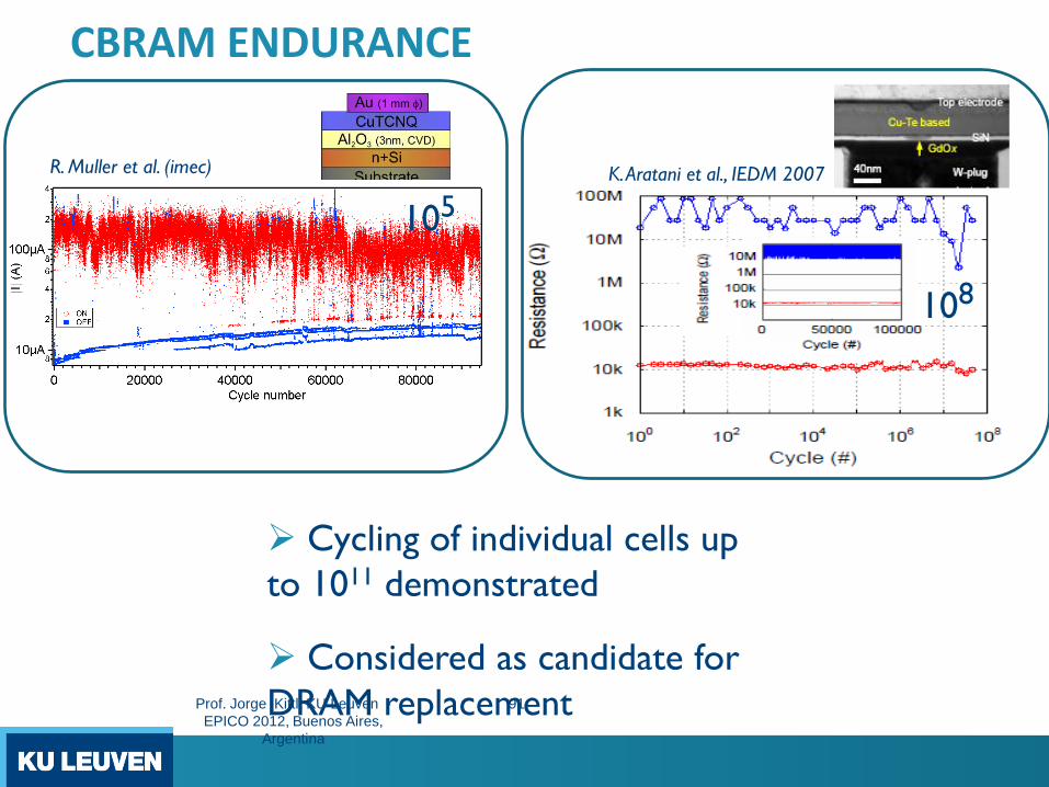
CBRAM ENDURANCE
K. Aratani et al., IEDM 2007 R. Muller et al. (imec)
105
108
Cycling of individual cells up
to 1011 demonstrated
Considered as candidate for
DRAM replacement 91 Prof. Jorge Kittl, KU Leuven -
EPICO 2012, Buenos Aires,
Argentina

CBRAM Scalability
Demonstration of the potential of the CBRAM technology on very small dimensions laying out a scalability path down to ~15nm
Source: Qimonda
Functionality down to 20 nm demonstrated
92 Prof. Jorge Kittl, KU Leuven -
EPICO 2012, Buenos Aires,
Argentina
1.E+03
1.E+05
1.E+07
1.E+09
1.E+00 1.E+01 1.E+02 1.E+03 1.E+04 1.E+05
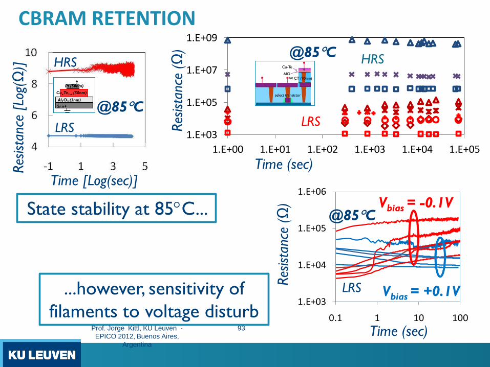
CBRAM RETENTION
W, BE W, BE
Al2O3CuTeTE TE
W CT (90nm)
select transistor
AlO
Cu-Te
Time [Log(sec)]
Res
ista
nce
[Lo
g(Ω
)]
LRS
HRS
@85C
1.E+03
1.E+04
1.E+05
1.E+06
0.1 1 10 100
Vbias = -0.1V
Time (sec)
Vbias = +0.1V Res
ista
nce
(Ω
) LRS
@85C
...however, sensitivity of
filaments to voltage disturb
Si n+
Al2O3 (3nm)
Pt (50nm)
CuxTe1-x (50nm)
State stability at 85C...
Time (sec) Res
ista
nce
(Ω
) @85C
LRS
HRS
93 Prof. Jorge Kittl, KU Leuven -
EPICO 2012, Buenos Aires,
Argentina
CBRAM CHALLENGES: THERMAL STABILITY AND RETENTION
High diffusivity metals used for fast switching (Ag,Cu)
with thermal budget, metal will tend to move leading to
challenges in:
Retention:
- dissolution of filament due to fast metal diffusion
Thermal stability (e.g. during processing)
- Excessive metal diffusion (shorts)
- Morphological degradation
- Phase separation (unacceptable for scaling)
- Adhesion issues
94 Prof. Jorge Kittl, KU Leuven -
EPICO 2012, Buenos Aires,
Argentina

ADDRESSING CBRAM CHALLENGES: THERMAL STABILITY AND RETENTION
x in CuxTe1-x
Form
ing
volt
age
(V)
Cell resistance (Ω
)
1030
5070
Intensity
2the
ta
Crys
tallin
ity(X
RD)
April
2010
1020304050607080
Te/(Te+Cu)
Comp
ositi
on
(XRF
) 30
50
Cu
Cu2Te
2()
Intensity (a.u.)
Cu2Te + CuCu2TeTe + CuTe
(a)
(b)
(c)
x=0.74x=0.67x=0.6x=0.35
amorphous Cu2Te-Crystal Cu inclusions
0.0E+00
5.0E+07
1.0E+08
1.5E+08
2.0E+08
2.5E+08
0
1
2
3
4
0.2 0.3 0.4 0.5 0.6 0.7 0.8
Forming voltageresistance
1.E-12
1.E-08
1.E-04
0 2.5 5
x>0.7
V(V)
I(A)
1030
5070
Intensity
2theta
Crys
tallin
ity(X
RD)
April
2010
1020304050607080
Te/(Te+Cu)
Comp
ositi
on
(XRF
) 30
50
Cu
Cu2Te
2()
Intensity (a.u.)
Cu2Te + CuCu2TeTe + CuTe
Cu-Te Cu2-xTe
CuCuTe
x=0.75x=0.6x=0.35
2
()
Intensity (a.u.)
amorphous Cu2Te-Crystal Cu inclusions
Cu-content
100 200 300 400 500 600 700 800 Temperature (oC)
2-T
he
ta (d
eg
) 20
25
30
35
200oC 200oC 200oC
IS-XRD
200oC 300oC
XRD
1.E+02
1.E+03
1.E+04
1.E+05
1.E+06
0 10 20 30 40
Inte
nsi
ty (C
ou
nts
/s)
Time (min)
Te
Cu
Al
1.E+02
1.E+03
1.E+04
1.E+05
1.E+06
0 10 20 30 40
Inte
nsi
ty (C
ou
nts
/s)
Time (min)
Te
Cu Al
200oC
Better morphology and thermal stability
by composition and stack optimization
Composition optimization Stack optimization (layers, alloying elements)
SIMS
200oC
95 Prof. Jorge Kittl, KU Leuven -
EPICO 2012, Buenos Aires,
Argentina

2D “Area Distributed” Systems
96 Prof. Jorge Kittl, KU Leuven -
EPICO 2012, Buenos Aires,
Argentina

97 Prof. Jorge Kittl, KU Leuven -
EPICO 2012, Buenos Aires,
Argentina
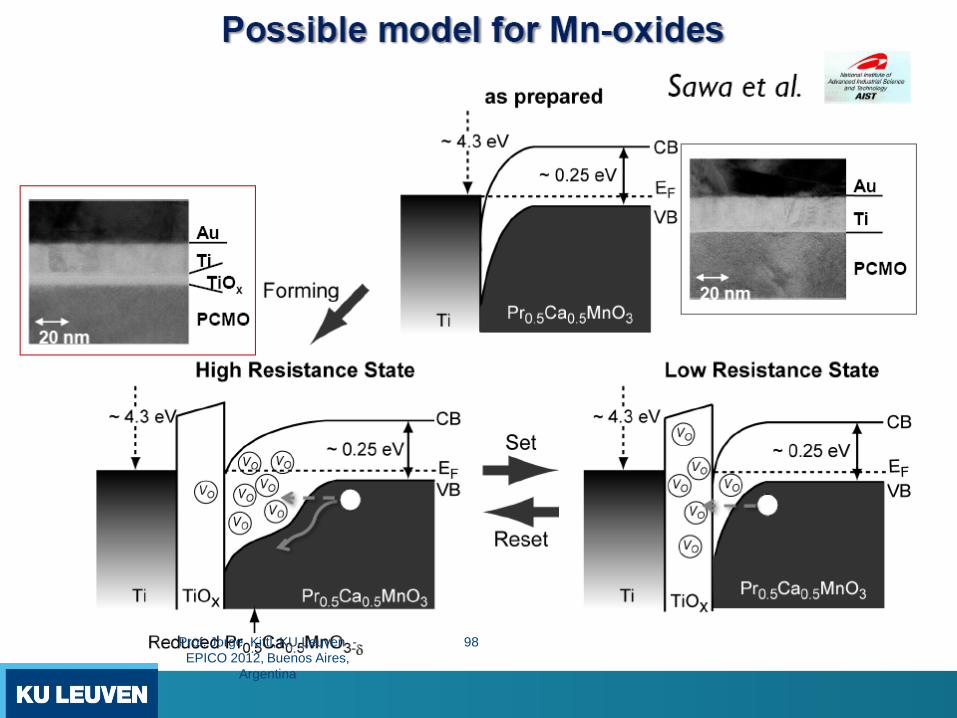
98 Prof. Jorge Kittl, KU Leuven -
EPICO 2012, Buenos Aires,
Argentina

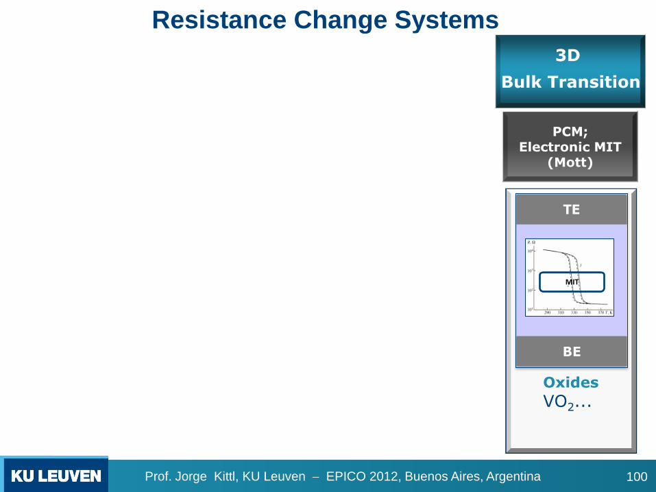
PCM; Electronic MIT
(Mott)
Cation motion, Electrochemical metallization, metal bridge
Ag, Cu based (Chalcogenide or oxide glasses
Oxides
VO2...
3D
Bulk Transition
Cation Source (Ag+, Cu+ or...)
Cu+
Ag+
BE
ME
TA
LIC
FIL
AM
EN
T
Interface barrier, Redox - vacancy
migration across interface
2D
Area Distributed
s/c Perovskites RE-CMO, Nb-STO....
TE
BE
MITMIT
TE
BE
exchange layer
O vacancy,...
perovskite
1D Filamentary
(narrow conduction path)
Local change in oxidation state (reduced state is more conductive)
Metal Oxides NiOx, HfOx, TiOx, TaOx...
TE
BE
metaloxide
reduced
Resistance Change systems
99 Prof. Jorge Kittl, KU Leuven - EPICO 2012, Buenos Aires, Argentina
PCM; Electronic MIT
(Mott)
Cation motion, Electrochemical metallization, metal bridge
Ag, Cu based (Chalcogenide or oxide glasses)
Oxides
VO2...
3D
Bulk Transition
Cation Source (Ag+, Cu+ or...)
Cu+
Ag+
BE
ME
TA
LIC
FIL
AM
EN
T
Interface barrier, Redox - vacancy
migration across interface
2D
Area Distributed
s/c Perovskites RE-CMO, Nb-STO....
TE
BE
MITMIT
TE
BE
exchange layer
O vacancy,...
perovskite
1D Filamentary
(narrow conduction path)
Local change in oxidation state (reduced state is more conductive)
Metal Oxides
TE
BE
metaloxide
reduced
Hf(Zr)Ox, NiOx, TiOx, TaOx...
Resistance Change Systems
100 Prof. Jorge Kittl, KU Leuven - EPICO 2012, Buenos Aires, Argentina

VO2 VO2 changes from semiconducting to
metallic at 68oC
Structural/Mott transition
Phase transformation occurs by local
displacements (V-V bond dilation) on a
fs/ps time scale, followed by long-range
shear rearrangements on sub-ns
timescale.
Switching in ns time scales possible
Switching devices demonstrated (but
device operation required holding voltage)
low-temp phase
Monoclinic VO2
Tetragonal VO2
high-temp phase
Kim et al.
Local atomic displacement
Shear
P. Baum et al., Science, 318, 788 (2007)
101 Prof. Jorge Kittl, KU Leuven - EPICO 2012, Buenos Aires, Argentina
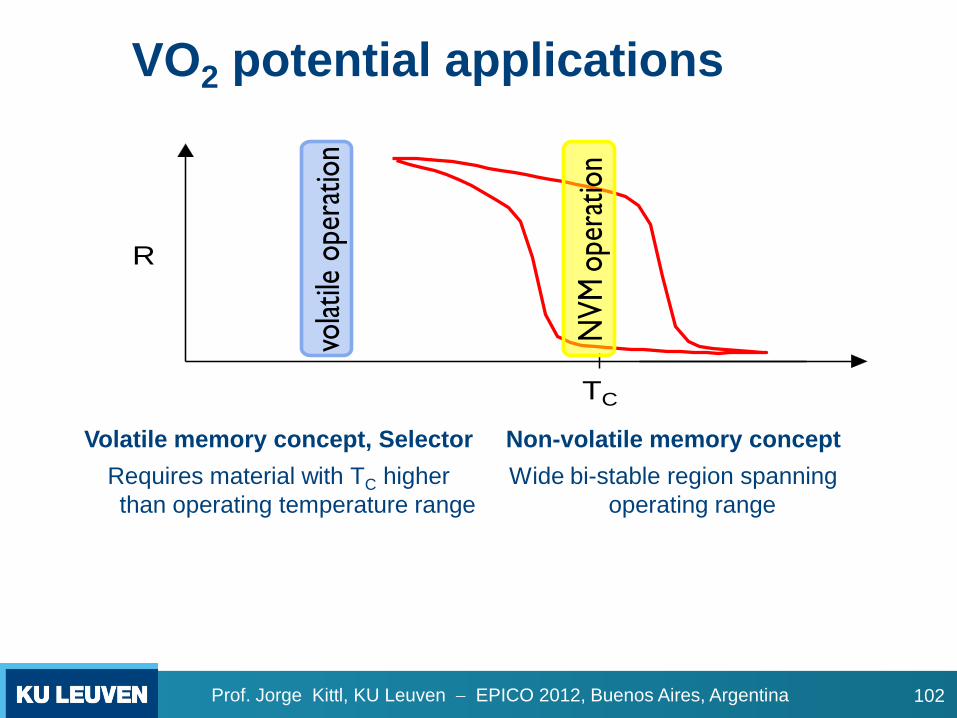
VO2 potential applications
Volatile memory concept, Selector
Requires material with TC higher
than operating temperature range
Non-volatile memory concept
Wide bi-stable region spanning
operating range
R
TC
vola
tile
oper
atio
n
NV
Mop
erat
ion
102 Prof. Jorge Kittl, KU Leuven - EPICO 2012, Buenos Aires, Argentina
0.001
0.01
0.1
1
10
Re
sis
tivity (
cm
)
12010080604020
T(°C)
Oct. 2010 Apr. 2010
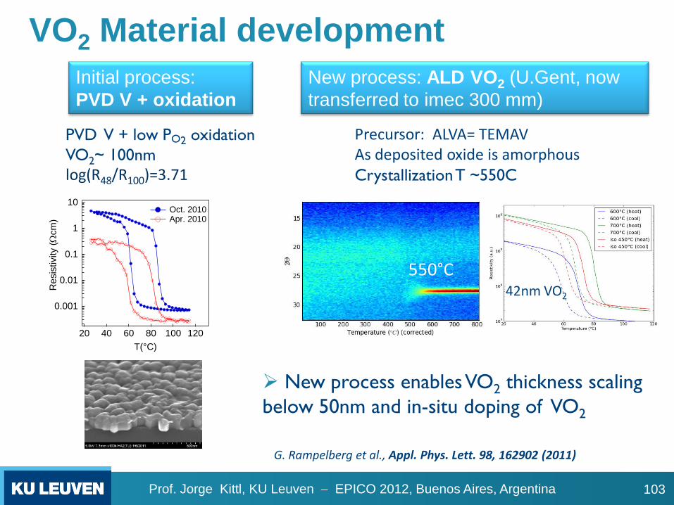
VO2 Material development
PVD V + low PO2 oxidation
VO2~ 100nm
log(R48/R100)=3.71
Initial process:
PVD V + oxidation
New process: ALD VO2 (U.Gent, now
transferred to imec 300 mm)
42nm VO2
Precursor: ALVA= TEMAV As deposited oxide is amorphous Crystallization T ~550C
550°C
New process enables VO2 thickness scaling
below 50nm and in-situ doping of VO2
G. Rampelberg et al., Appl. Phys. Lett. 98, 162902 (2011)
103 Prof. Jorge Kittl, KU Leuven - EPICO 2012, Buenos Aires, Argentina
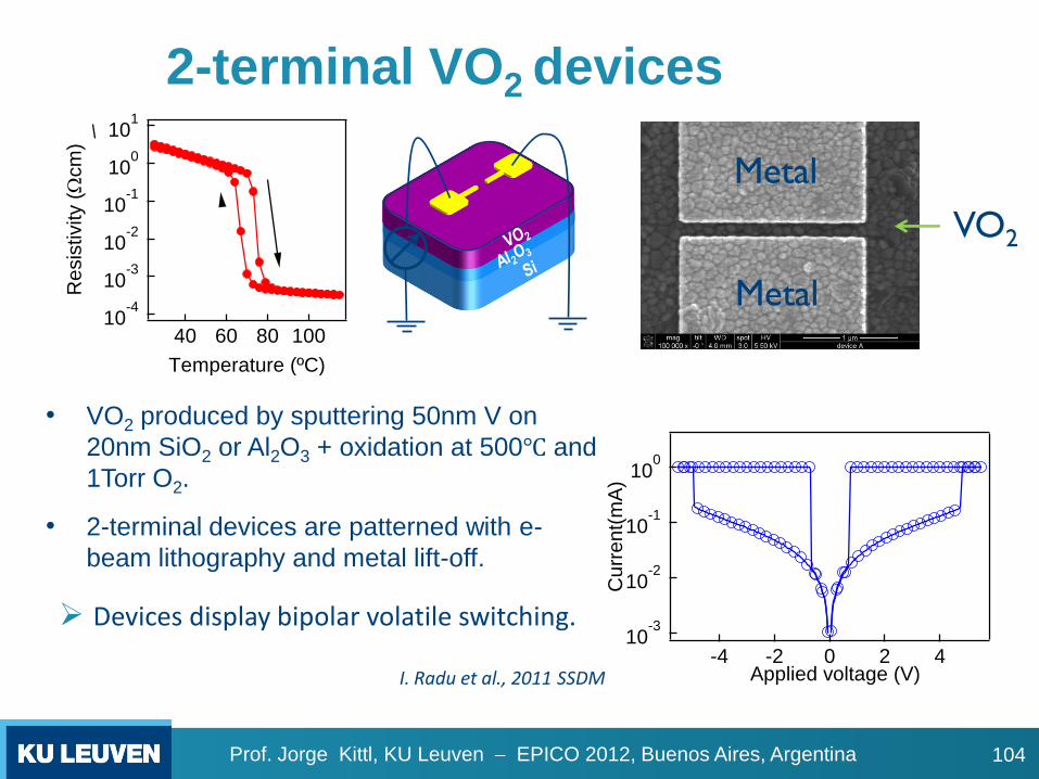
2-terminal VO2 devices
• VO2 produced by sputtering 50nm V on
20nm SiO2 or Al2O3 + oxidation at 500 and
1Torr O2.
• 2-terminal devices are patterned with e-
beam lithography and metal lift-off.
10-4
10-3
10-2
10-1
100
101
Re
sis
tivity (
cm
)
100806040
Temperature (ºC)
10-3
10-2
10-1
100
Cu
rre
nt(
mA
)
-4 -2 0 2 4Applied voltage (V)
Metal
Metal
VO2
Devices display bipolar volatile switching.
I. Radu et al., 2011 SSDM
104 Prof. Jorge Kittl, KU Leuven - EPICO 2012, Buenos Aires, Argentina
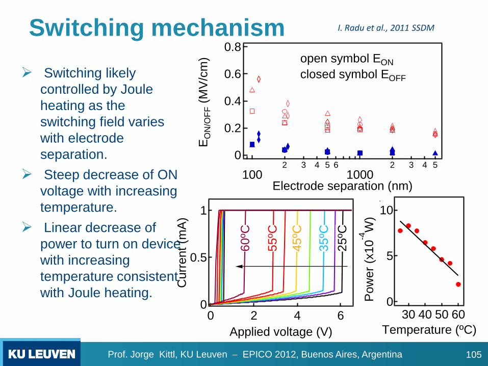
Switching mechanism
Switching likely
controlled by Joule
heating as the
switching field varies
with electrode
separation.
Steep decrease of ON
voltage with increasing
temperature.
Linear decrease of
power to turn on device
with increasing
temperature consistent
with Joule heating.
10
5
0Pow
er
(x10
-4W
)
60504030
Temperature (ºC)
1
0.5
0
Curr
ent
(mA
)
6420
Applied voltage (V)2
5ºC
60ºC
45ºC
35ºC
55ºC
0.8
0.6
0.4
0.2
0
EO
N/O
FF (
MV
/cm
)
1002 3 4 5 6
10002 3 4 5
Electrode separation (nm)
open symbol EON
closed symbol EOFF
I. Radu et al., 2011 SSDM
105 Prof. Jorge Kittl, KU Leuven - EPICO 2012, Buenos Aires, Argentina
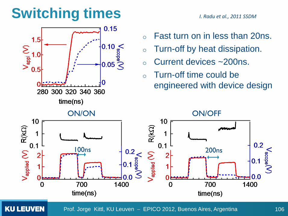
Switching times
o Fast turn on in less than 20ns.
o Turn-off by heat dissipation.
o Current devices ~200ns.
o Turn-off time could be
engineered with device design
ON/ON ON/OFF
100ns 200ns
I. Radu et al., 2011 SSDM
106 Prof. Jorge Kittl, KU Leuven - EPICO 2012, Buenos Aires, Argentina

Endurance • ROFF/RON~100
• Stable over more than 1010 cycles (device still
working when endurance testing stopped).
4
102
2
4
103
2
4
104
R (
)
102 10
4 106 10
8 1010
cycle #
I. Radu et al., 2011 SSDM
107 Prof. Jorge Kittl, KU Leuven - EPICO 2012, Buenos Aires, Argentina

Volatile switching
Joule heating
induced switching in
2 terminal devices
Volatile, symmetric,
excellent cyclability
VO2 devices
Isothermal (68 )
retention time:
Excellent retention to 10
years within hysteresis
loop
4
102
2
4
103
2
4
104
R (
)
102 10
4 106 10
8 1010
cycle #
10-3
10-2
10-1
100
Cu
rre
nt(
mA
)
-4 -2 0 2 4Applied voltage (V)
108 Prof. Jorge Kittl, KU Leuven - EPICO 2012, Buenos Aires, Argentina
Summary
109 Prof. Jorge Kittl, KU Leuven - EPICO 2012, Buenos Aires, Argentina
Thank you for your attention
Gracias a Pablo y a todos los organizadores!
110 Prof. Jorge Kittl, KU Leuven - EPICO 2012, Buenos Aires, Argentina
Thank you for your attention
Gracias a Pablo y a todos los organizadores!
Appl. Phys. Lett. 99, 053502 (2011) Appl. Phys. Lett. 100, 113513 (2012)
TECu-sourceCu+
Cu+
Cu+
Cu+
BE
90nm CBRAM stack
OPTIMUM Cu-Te COMPOSITION
Voltage (V)
Curr
ent (A
)
(2) 0.5<x<0.7
-1.0 -0.5 0.0 0.51E-10
1E-9
1E-8
1E-7
1E-6
1E-5
Si n+
Al2O3 (3nm)
Pt (50nm)
CuxTe1-x (50nm)
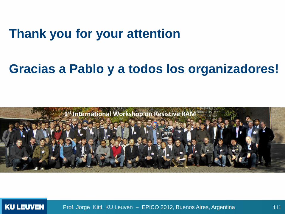
1st International Workshop on Resistive RAM
111 Prof. Jorge Kittl, KU Leuven - EPICO 2012, Buenos Aires, Argentina