prof. daniel costinett
TRANSCRIPT

1/31/2017
Power Electronics Circuits
Prof. Daniel Costinett
ECE 482 Lecture 3January 26, 2017
Announcements
• Experiment 1 Report Due Tuesday
• Prelab 3 due Thursday
• All assignments turned in digitally
− By e‐mailing to [email protected]
− Include [ECE 482] in the subject
• Parts kit purchased prior to Tuesday’s class
• Capture waveforms, even if something is malfunctioning, for report

1/31/2017
Outline
1. Motor Back EMF Shape
2. Power Converter Layout
3. Loss Analysis and Design
– Low Frequency Conduction Losses
– Inductor AC Losses
– Core Losses
– Inductor Design Approaches
BACK EMF SHAPE
PMSM vs BLDC
1/31/2017
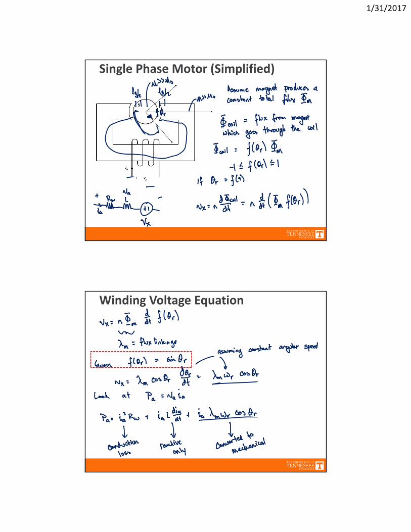
Single Phase Motor (Simplified)
Winding Voltage Equation

1/31/2017
– Sinusoidal back EMF achieved with sinusoidal winding distribution
– Generally termed Permanent Magnet Synchronous Motor (PMSM)
Shape of Back EMF – PMSM Winding
http://web.eecs.utk.edu/courses/spring2017/ece482/materials/brushless‐motor.swf
BLDC Motor Winding
– Brushless DC (BLDC) Motors are not wound sinusoidally
– This results in Trapezoidal back emf, rather than sinusoidal
– Can be driven simply with Square‐waves to achieve relatively low torque ripple

1/31/2017
Outer‐ vs. Inner‐Rotor
• Traditional motors are inner‐rotor• On e‐bike, need hub to remain stationary and outer wheel to spin
Motor Teeth/Poles Example

1/31/2017
56 pole63 teeth
Stator Winding
Complete winding of Phase A Complete winding of all phases
Rotor and Poles
• Outer rotor (to which spokes/wheel are attached)
• Magnets alternate N‐S

1/31/2017
0 5 10 15 20 25 30-8
-6
-4
-2
0
2
4
6
8
theta [deg]
Nor
mal
ized
Cou
pled
Flu
x [T
esla
*coi
l]
• 33 Teeth, 22 Poles• Teeth/Pole/Phase = 0.5
ABC
S N
stator
rotor
Shape of Back EMF
0 5 10 15 20 25 30-8
-6
-4
-2
0
2
4
6
8
theta [deg]
Nor
mal
ized
Cou
pled
Flu
x [T
esla
*coi
l]
• 36 Teeth, 22 Poles• Teeth/Pole/Phase = 0.5455
ABC
S N
stator
rotor
Shape of Back EMF
1/31/2017
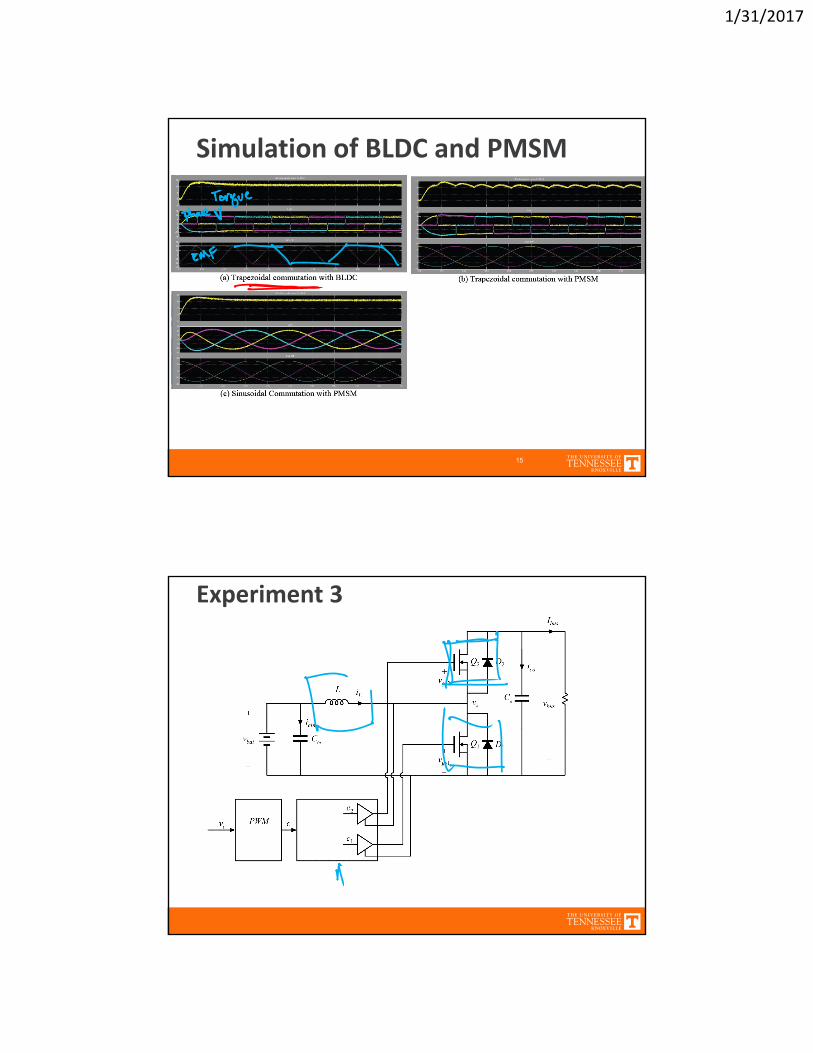
Simulation of BLDC and PMSM
15
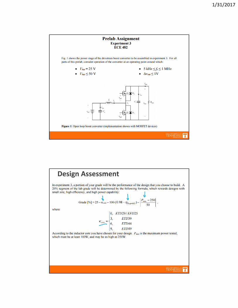
Experiment 3
1/31/2017
Design Assessment
1/31/2017
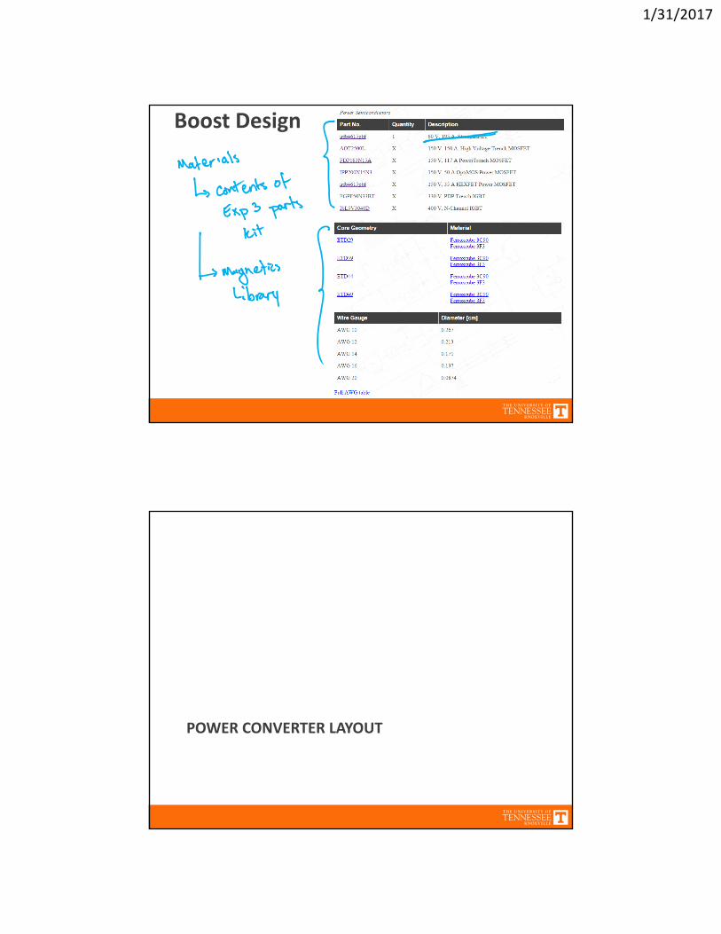
Boost Design
POWER CONVERTER LAYOUT
1/31/2017
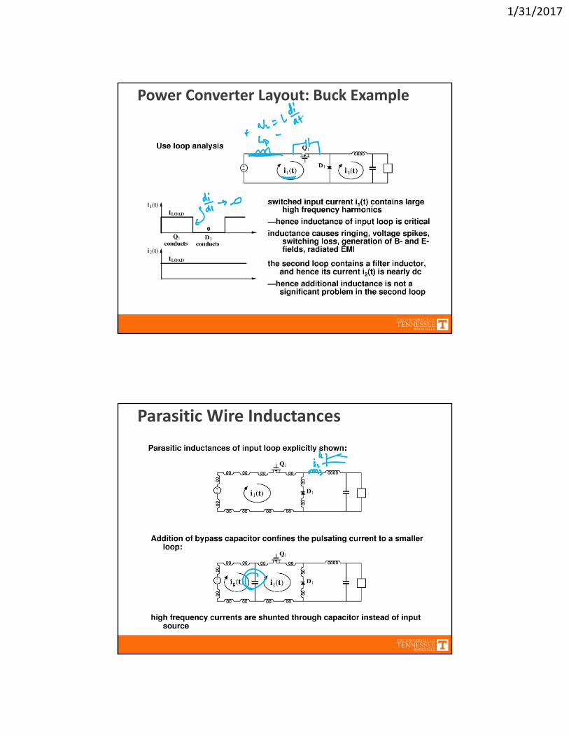
Power Converter Layout: Buck Example
Parasitic Wire Inductances
1/31/2017
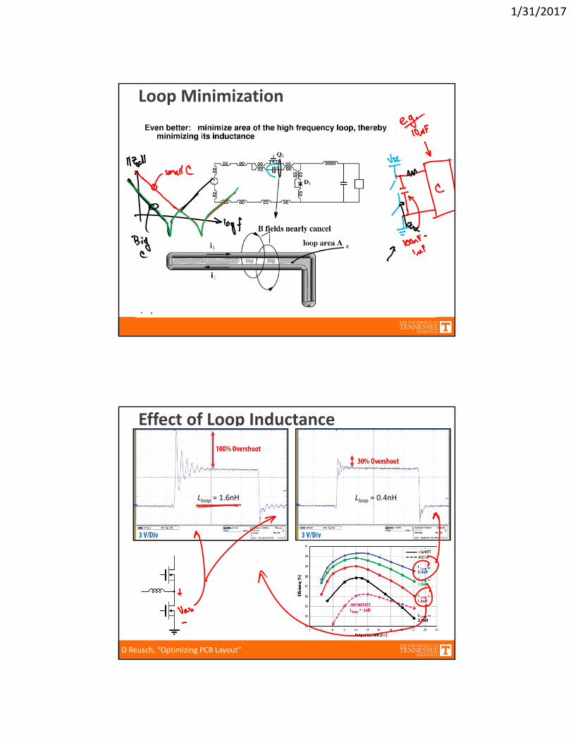
Loop Minimization
Effect of Loop Inductance
D Reusch, “Optimizing PCB Layout”
Lloop = 0.4nHLloop = 1.6nH

1/31/2017
• Gate driver chip must implement vgs waveforms• Sources will have pulsating currents and need decoupling
Half Bridge Gate Drive Waveforms
• MOSFET is off when vgs < Vth ≈ 3 V
• MOSFET fully on when vgs is sufficiently large (10‐15 V)
• Warning: MOSFET gate oxide breaks down and the device fails when vgs> 20 V.
• Fast turn on or turn off (10’s of ns) requires a large spike (1‐2 A) of gate current to charge or discharge the gate capacitance
• MOSFET gate driver is a logic buffer that has high output current capability
2
8
~100
Driving a Power MOSFET Switch

1/31/2017
PWM Pulsesfrom controller/ Fcn Generator
Source
Drain
Gate
• MOSFET gate driver is used as a logic buffer with high output current (~1.8 A) capability• The amplitude of the gate voltage equals the supply voltage VCC• Decoupling capacitors are necessary at all supply pins of LM5104 (and all ICs)• Gate resistance used to slow dv/dt at switch node
Driving a Power MOSFET Switch
• Gate driver is cascades back half‐bridges of decreasing size to obtain quick rise times
• Reminder: keep loops which handle pulsating current small by decoupling and making close connections
Gate Drive Implementation

1/31/2017
Decoupling
• Always add bypass capacitor at power supply for any IC/reference
• Use small‐valued (~100nf), low ESR and ESL capacitors (ceramic)
• Limit loop for any di/dt
• Area of current pulse is total charge supplied to gate of capacitor
• All charge must be supplied from gate drive decoupling capacitor
Δ
Capacitor Sizing Notes

1/31/2017
• Gate charge is supplied through driver resistance during switch turn‐on
• Gate charge is dissipated in gate driver on switch turn‐off
,
Gate Drive Losses
• Gate driver chip must implement vgs waveforms• Issue: source of Q2 is not grounded
High Side Signal Ground

1/31/2017
• Isolated supplies sometimes used; Isolated DC‐DC, batteries
• Bootstrap concept: capacitor can be charged when Vsis low, then switched
Generating Floating Supply
A Note on Grounding

1/31/2017
UCC27211a Internal Diagram
Fairchild Semi App Note AN‐6076

1/31/2017
Parasitics to be Aware of
Power Loop Inductances
Persson E., “What really limits MOSFET performance: silicon, package, driver or circuit board?”

1/31/2017
Complete Routing of Signal
• Always consider return path
• Ground plane can help, but still need to consider the path and optimize
Star‐Grounding Vs. Daisy Chain
1/31/2017
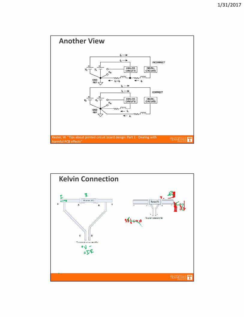
Another View
Kester, W. “Tips about printed circuit board design: Part 1 ‐ Dealing with harmful PCB effects”
Kelvin Connection

1/31/2017
Efficiency Measurement
Boost Converter
POWER CONVERTER DESIGN AND LOSS ANALYSIS

1/31/2017
Converter Design
MOSFET Selection
InductorDesign
SwitchingFrequency
Thermal Model
Cost Model
Loss Model
...
DesignSpecifications
PerformanceSpecification
Design Assessment
Analytical Model
Analytical Loss Modeling
• High efficiency approximation is acceptable for hand calculations, as long as it is justified
• Solve ideal waveforms of lossless converter, then calculate losses
• Argue which losses need to be included, and which may be neglected
• “Rough” approximation to gain insight into significance

1/31/2017
Additional Resources
• Additional lectures in ECE581
− http://web.eecs.utk.edu/~dcostine/ECE581/Fall2016/schedule.php
− Accessible only from campus network
• Switching Overlap Loss L4‐L5
• Device Capacitances L6‐L7
• Magnetics Losses L19(2nd half) and L20
• Begin by solving important waveforms throughout converter assuming lossless operation
Boost Converter Loss Analysis

1/31/2017
MOSFETS Body Diodes Inductor Capacitors
• Ron • VF
• Rd
• Rdc • ESR
• Coss• Overlap• Pg
• Td cond.• Cd• Reverse‐
Recovery
• Skin Effect• Core Loss• Fringing• Proximity
• Dielectric Losses
Low‐Frequency Losses
Frequency‐Dependent Losses
Power Stage Losses
LOW FREQUENCY CONDUCTION LOSSES

1/31/2017
• Considering only power stage losses (gate drive neglected)
• MOSFET operated as power switch• Intrinsic body diode behaviors considered using normal diode analysis
MOSFET Equivalent Circuit
• On resistance extracted from datasheet waveforms• Significantly dependent on Vgs amplitude, temperature
1
MOSFET On Resistance
1/31/2017
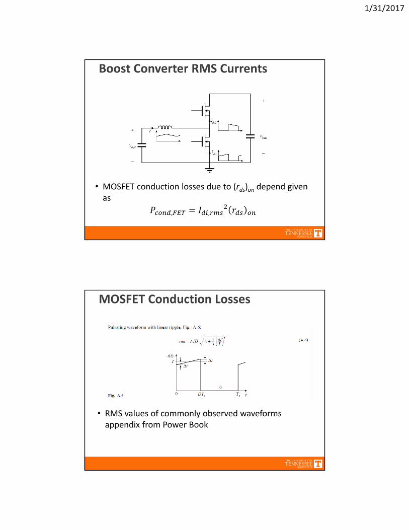
• MOSFET conduction losses due to (rds)on depend given as
, ,
Boost Converter RMS Currents
• RMS values of commonly observed waveforms appendix from Power Book
MOSFET Conduction Losses

1/31/2017
• Operation well below resonance• All loss mechanisms in a capacitor are generally lumped into an empirical loss model
• Equivalent Series Resistance (ESR) is highly frequency dependent
• Datasheets may give effective impedance at a frequency, or loss factor:
2tan
‐
Capacitor Loss Model
• DC Resistance given by
• At room temp, ρ = 1.724∙10‐6Ω‐cm• At 100°C, ρ = 2.3∙10‐6Ω‐cm
• Losses due to DC current:
, ,
DC Inductor Resistance
1/31/2017
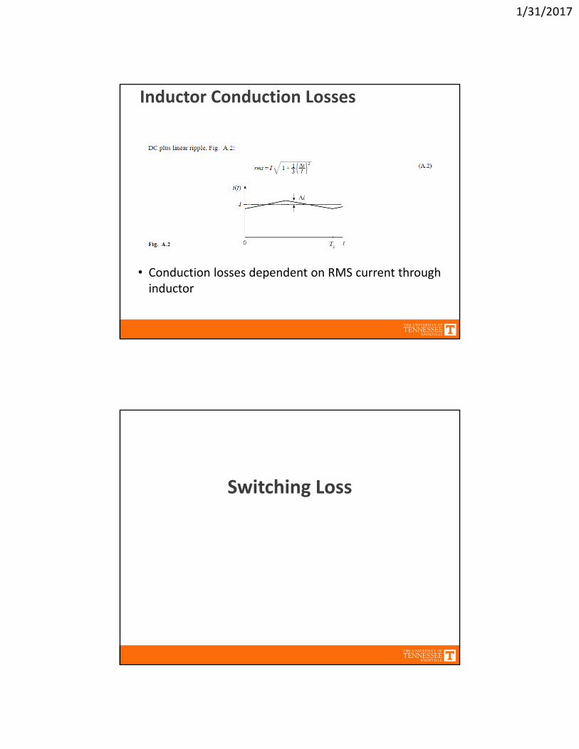
• Conduction losses dependent on RMS current through inductor
Inductor Conduction Losses
Switching Loss
1/31/2017
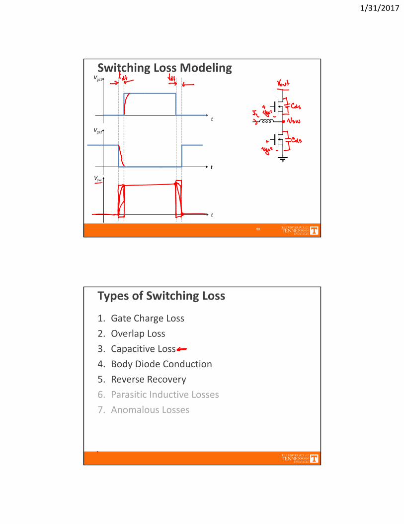
Switching Loss Modeling
59
Vgs1
Vgs2
t
t
Vsw
t
Types of Switching Loss
1. Gate Charge Loss
2. Overlap Loss
3. Capacitive Loss
4. Body Diode Conduction
5. Reverse Recovery
6. Parasitic Inductive Losses
7. Anomalous Losses
1/31/2017
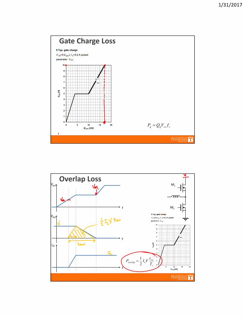
Gate Charge Loss
sccgg fVQP
Overlap LossVgs2
Vds2
id2
t
t
ts
swLoverlap T
tVIP
2
1
M2
M1
1/31/2017
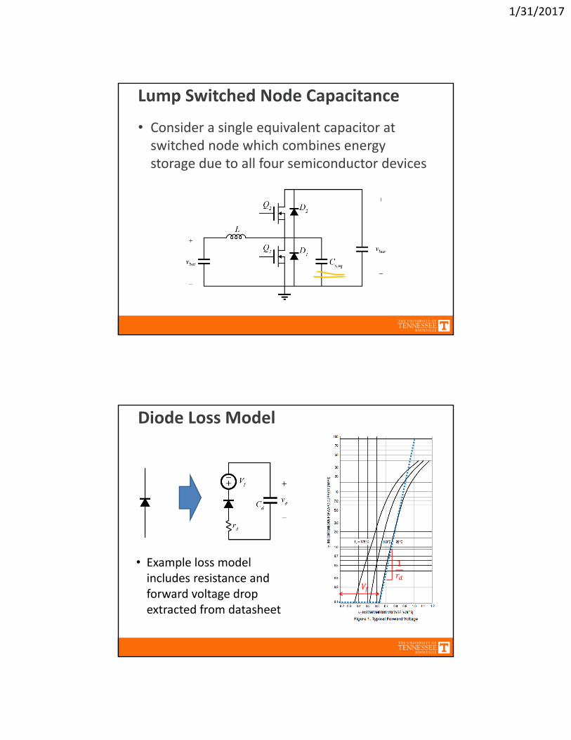
Lump Switched Node Capacitance
• Consider a single equivalent capacitor at switched node which combines energy storage due to all four semiconductor devices
1• Example loss model includes resistance and forward voltage drop extracted from datasheet
Diode Loss Model

1/31/2017
Diode Reverse Recovery
• Diodes will turn on during dead time intervals
• Significant reverse recovery possible on both body diode and external diode
busrrrrLLrron VQtiIE ,
INDUCTOR AC LOSSES

1/31/2017
• Current profile at high frequency is exponential function of distance from center with characteristic length δ
Skin Effect in Copper Wire
rw
δ
,
,
AC Resistance

1/31/2017
Skin Depth
• In foil conductor closely spaced with h >> δ, flux between layers generates additional current according to Lentz’s law.
• Power loss in layer 2:
• Needs modification for non‐foil conductors
,
, + 2 ,
5
Proximity Effect
See Fundamentals of Power Electronics, Section 13.4
1/31/2017
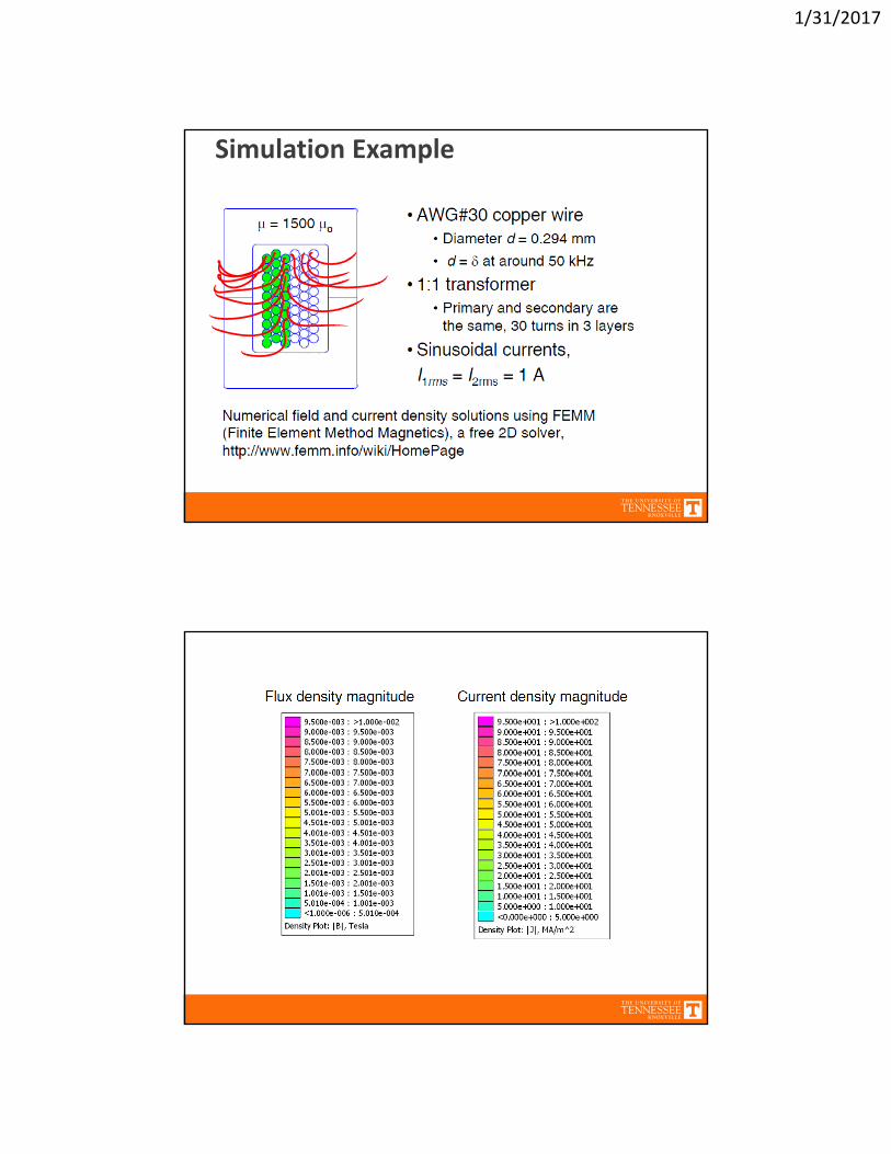
Simulation Example

1/31/2017
Frequency: 1 kHz
Frequency: 100 kHz

1/31/2017
Frequency: 1 MHz
Frequency: 10 MHz
1/31/2017
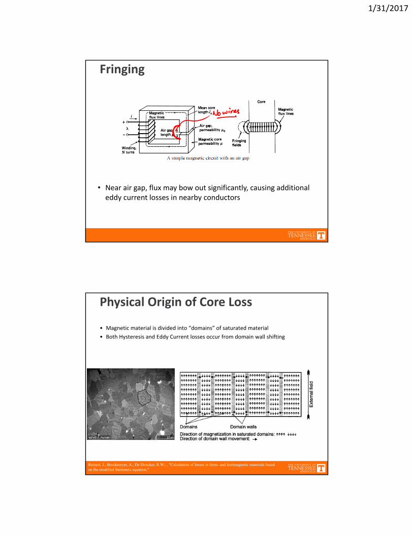
• Near air gap, flux may bow out significantly, causing additional eddy current losses in nearby conductors
Fringing
Physical Origin of Core Loss
• Magnetic material is divided into “domains” of saturated material
• Both Hysteresis and Eddy Current losses occur from domain wall shifting
Reinert, J.; Brockmeyer, A.; De Doncker, R.W.; , "Calculation of losses in ferro- and ferrimagnetic materials based on the modified Steinmetz equation,"

1/31/2017
Inductor Core Loss
• Governed by Steinmetz Equation:
• Parameters Kfe, α, and βextracted from manufacturer data
• Δ ∝ Δ → small losses with small ripple
Δ [mW/cm3]
[mW]
Steinmetz Parameter Extraction
1/31/2017
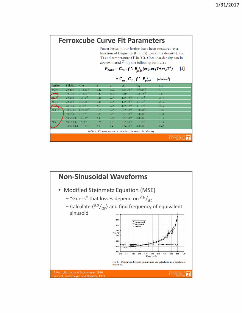
Ferroxcube Curve Fit Parameters
Non‐Sinusoidal Waveforms
• Modified Steinmetz Equation (MSE)
− “Guess” that losses depend on ⁄
− Calculate ⁄ and find frequency of equivalent sinusoid
Albach ,Durbau and Brockmeyer, 1996 Reinert, Brockmeyer, and Doncker, 1999

1/31/2017
NSE/iGSE
Van den Bossche, A.; Valchev, V.C.; Georgiev, G.B.; , "Measurement and loss model of ferrites with non‐sinusoidal waveforms,“K. Venkatachalam; C. R. Sullivan; T. Abdallah; H. Tacca, “Accurate prediction of ferrite core loss with nonsinusoidal waveforms using only
Steinmetz parameters”
Simple Formula for Square‐wave voltages:
INDUCTOR DESIGN
1/31/2017
Inductor Design
Freedoms:
1. Core Size and Material
2. Number of turns and wire gauge
3. Length of Air Gap
Constraints:
1. Obtain Designed L
2. Prevent Saturation
3. Minimize Losses
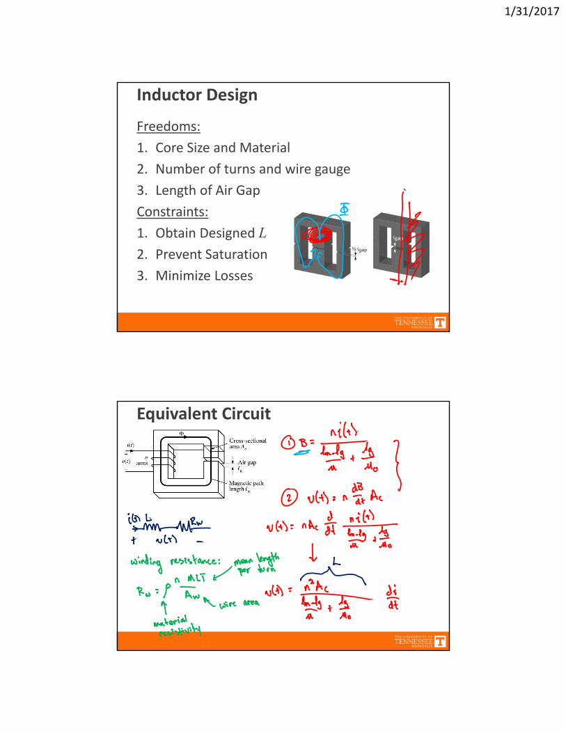
Equivalent Circuit
1/31/2017
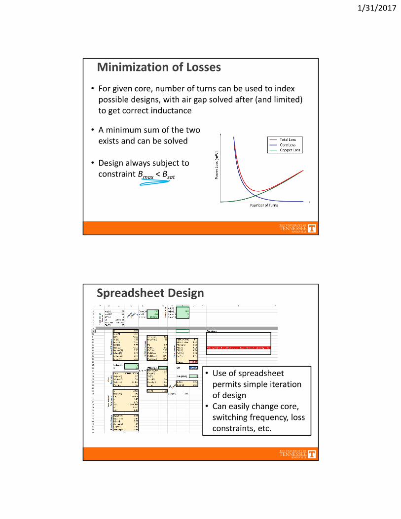
• For given core, number of turns can be used to index possible designs, with air gap solved after (and limited) to get correct inductance
• A minimum sum of the two exists and can be solved
• Design always subject to constraint Bmax < Bsat
Minimization of Losses
Spreadsheet Design
• Use of spreadsheet permits simple iteration of design
• Can easily change core, switching frequency, loss constraints, etc.
1/31/2017
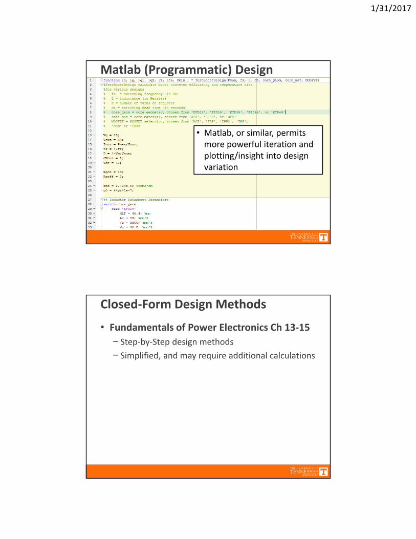
Matlab (Programmatic) Design
• Matlab, or similar, permits more powerful iteration and plotting/insight into design variation
Closed‐Form Design Methods
• Fundamentals of Power Electronics Ch 13‐15
− Step‐by‐Step design methods
− Simplified, and may require additional calculations

1/31/2017
Kg Kgfe
Losses DC Copper (specified)
DC Copper,SE Core Loss (optimized)
Saturation Specified Checked After
Bmax Specified Optimized
Kg and Kgfe Methods
• Two closed‐form methods to solve for the optimal inductor design under certain constraints/assumptions
• Neither method considers losses other than DC copper and (possibly) steinmetz core loss
• Both methods particularly well suited to spreadsheet/iterative design procedures
• Method useful for filter inductors where ΔB is small• Core loss is not included, but may be significant particularly if large ripple is present
• Copper loss is specified through a set target resistance• The desired Bmax is given as a constraint• Method does not check feasibility of design; must ensure that air gap is not extremely large or wire size excessively small
• Simple first‐cut design technique; useful for determining approximate core size required
• Step‐by‐step design procedure included on website
Kg Method

1/31/2017
• Method useful for cases when core loss and copper loss are expected to be significant
• Saturation is not included in the method, rather it must be checked afterward
• Enforces a design where the sum of core and copper is minimized
Kgfe Method
1/31/2017
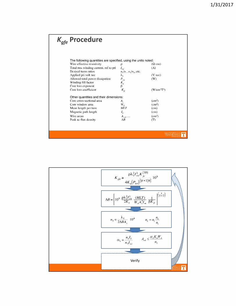
Kgfe Procedure
2
2
n
WKA Auwk
11 n
nnn k
k
Verify

1/31/2017
Kgfe Method: Summary
• Method enforces an operating ΔB in which core and copper losses are minimized
• Only takes into account losses from standard Steinmetz equation; not correct unless waveforms are sinusoidal
• Does not consider high frequency losses• Step‐by‐step design procedure included on website