production and processing of graphene and 2d crystals · cost-effective production methods are...
TRANSCRIPT

564 ISSN:1369 7021 © Elsevier Ltd 2012DECEMBER 2012 | VOLUME 15 | NUMBER 12
Graphene has high mobility and optical transparency, in addition to flexibility, high mechanical strength and environmental stability. These properties have already had a huge impact on fundamental science1-3, and are making graphene and graphene-based materials a promising platform for electronics, composites, sensors, spintronics, photonics and optoelectronics1,4,5. A variety of possible applications ranging from solar cells6 and light-emitting devices7,8 to touch screens9, photodetectors10-13, ultrafast lasers14,15, membranes16,17, spin valves18,19, high frequency electronics20, etc. are being explored. The present ”second phase” of graphene research, after the award of the Nobel Prize to Geim and Novoselov, besides deepening the understanding of the fundamental aspects of this material, should target applications and manufacturing processes, and broaden research to other two-dimensional (2d) materials and hybrid systems. Graphene development could impact products in multiple industries, from flexible, wearable and transparent electronics, to high performance computing and spintronics. The integration of these new materials could bring a new dimension to future technologies, where faster, thinner, stronger, flexible, and broadband devices are needed21. However, large-scale cost-effective production methods are required with a balance
between ease of fabrication and materials quality.Here we review the state of the art of graphene preparation, production, placement and handling, and outline how similar approaches could be used for other 2d crystals. The main approaches are summarized in Fig. 1. This paper is organized as follows. in section I we outline all the graphene production techniques, section II is dedicated to graphene processing after production, while in section III we discuss the development of inorganic layered compounds and hybrid structures. Table 1 gives a list of acronyms and notation used throughout the paper.
Section I: Graphene productionI.1 Dry exfoliationDry exfoliation is the splitting of layered materials (LM) into atomically thin sheets via mechanical, electrostatic, or electromagnetic forces in air, vacuum or inert environments.
I.1.1 Micromechanical cleavageMicromechanical cleavage (MC), also known as micromechanical exfoliation, has been used for decades by crystal growers and crystallographers22,23. In 1999, reference 24 reported a controlled method of cleaving graphite,
Production and processing of graphene and 2d crystals
Graphene is at the center of an ever growing research effort due to its unique properties, interesting for both fundamental science and applications. A key requirement for applications is the development of industrial-scale, reliable, inexpensive production processes. Here we review the state of the art of graphene preparation, production, placement and handling. Graphene is just the first of a new class of two dimensional materials, derived from layered bulk crystals. Most of the approaches used for graphene can be extended to these crystals, accelerating their journey towards applications.
Francesco Bonaccorso1, Antonio Lombardo1, Tawfique Hasan1, Zhipei Sun1, Luigi Colombo2, and Andrea C. Ferrari1,*
1Cambridge University, Engineering Department, 9 JJ Thomson Avenue, Cambridge CB3 0FA, UK2Texas Instruments Incorporated, 13121 TI Boulevard, Dallas, Texas 75243, USA*E-mail: [email protected]
565
Production and processing of graphene and 2d crystals EXTENDED REVIEW
DECEMBER 2012 | VOLUME 15 | NUMBER 12
(a)
(d)
(g)
(b)
(e)
(h)
(c)
(f)
(i)
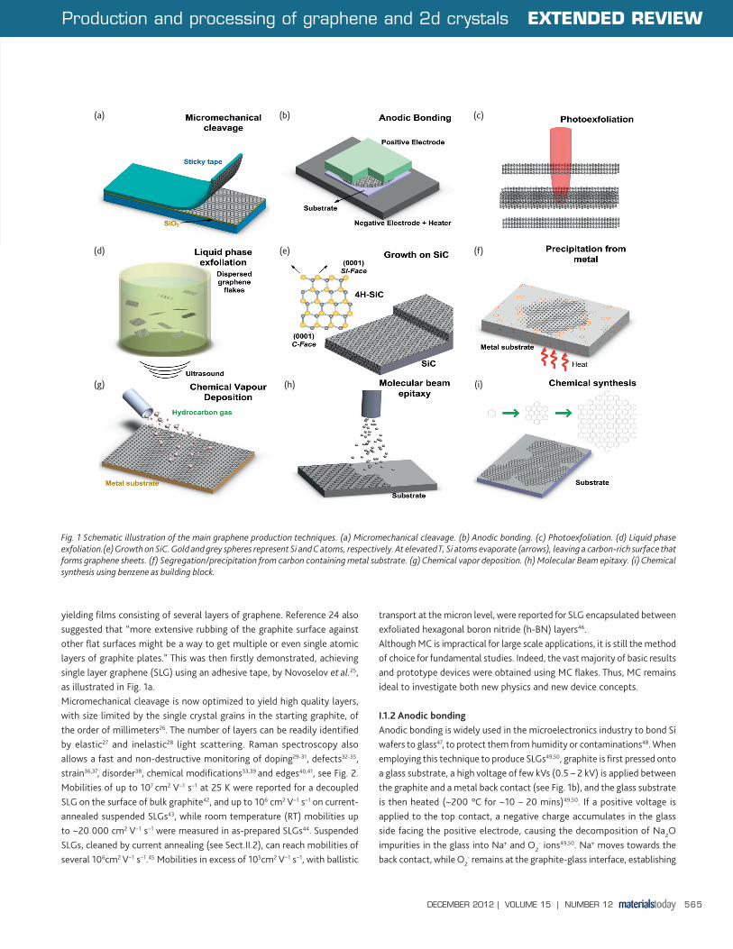
yielding films consisting of several layers of graphene. Reference 24 also suggested that “more extensive rubbing of the graphite surface against other flat surfaces might be a way to get multiple or even single atomic layers of graphite plates.” This was then firstly demonstrated, achieving single layer graphene (SLG) using an adhesive tape, by Novoselov et al.25, as illustrated in Fig. 1a.Micromechanical cleavage is now optimized to yield high quality layers, with size limited by the single crystal grains in the starting graphite, of the order of millimeters26. The number of layers can be readily identified by elastic27 and inelastic28 light scattering. Raman spectroscopy also allows a fast and non-destructive monitoring of doping29-31, defects32-35, strain36,37, disorder38, chemical modifications33,39 and edges40,41, see Fig. 2. Mobilities of up to 107 cm2 V−1 s−1 at 25 K were reported for a decoupled SLG on the surface of bulk graphite42, and up to 106 cm2 V−1 s−1 on current-annealed suspended SLGs43, while room temperature (RT) mobilities up to ~20 000 cm2 V−1 s−1 were measured in as-prepared SLGs44. Suspended SLGs, cleaned by current annealing (see Sect.II.2), can reach mobilities of several 106cm2 V−1 s−1.45 Mobilities in excess of 105cm2 V−1 s−1, with ballistic
transport at the micron level, were reported for SLG encapsulated between exfoliated hexagonal boron nitride (h-BN) layers46.Although MC is impractical for large scale applications, it is still the method of choice for fundamental studies. Indeed, the vast majority of basic results and prototype devices were obtained using MC flakes. Thus, MC remains ideal to investigate both new physics and new device concepts.
I.1.2 Anodic bondingAnodic bonding is widely used in the microelectronics industry to bond Si wafers to glass47, to protect them from humidity or contaminations48. When employing this technique to produce SLGs49,50, graphite is first pressed onto a glass substrate, a high voltage of few kVs (0.5 – 2 kV) is applied between the graphite and a metal back contact (see Fig. 1b), and the glass substrate is then heated (~200 °C for ~10 – 20 mins)49,50. If a positive voltage is applied to the top contact, a negative charge accumulates in the glass side facing the positive electrode, causing the decomposition of Na2O impurities in the glass into Na+ and O2
- ions49,50. Na+ moves towards the back contact, while O2
- remains at the graphite-glass interface, establishing
Fig. 1 Schematic illustration of the main graphene production techniques. (a) Micromechanical cleavage. (b) Anodic bonding. (c) Photoexfoliation. (d) Liquid phase exfoliation.(e) Growth on SiC. Gold and grey spheres represent Si and C atoms, respectively. At elevated T, Si atoms evaporate (arrows), leaving a carbon-rich surface that forms graphene sheets. (f) Segregation/precipitation from carbon containing metal substrate. (g) Chemical vapor deposition. (h) Molecular Beam epitaxy. (i) Chemical synthesis using benzene as building block.

566
EXTENDED REVIEW Production and processing of graphene and 2d crystals
DECEMBER 2012 | VOLUME 15 | NUMBER 12
Table 1. List of acronymsAcronym Definition Acronym Definition1LG Single layer graphene MLG Multilayer graphene2D Raman 2D peak ν Viscosity2d Two dimensional N Number of graphene layers3d Three dimensional NEMS Nanoelectromechanical system3LG Trilayer graphene NLG N-layer grapheneα Absorption coefficient NMP N-MethylPyrrolidonea-C Amorphous carbon NR Nanoribbona-C:H Hydrogenated amorphous carbon OAS Optical absorption spectroscopyAFM Atomic force microscopy PAH Polycyclic aromatic hydrocarbonsALD Atomic layer deposition PDMS Poly(dimethylsiloxane)ALE Atomic layer epitaxy PECVD Plasma enhanced chemical vapor depositionBLG Bi-layer graphene PEG Poly(ethylene glycol)BMIMPF6 1-Butyl-3-methylimidazolium hex-afluorophosphate PET Poly(ethylene terephthalate)BN Boron nitride PL Photoluminescencec Concentration PMMA Poly(methyl methacrylate)CBE Chemical beam epitaxy PTCDA Perylene-3,4,9,10-tetracarboxylic dianhydrideCMOS Complementary metal-oxide semiconductor PV PhotovoltaicCNT Carbon nanotube PVD Physical vapor depositionCVD Chemical vapor deposition QHE Quantum Hall effectDEP Dielectrophoresis ρ DensityDGM Density gradient medium R2R Roll to rollDGU Density gradient ultracentrifugation RCA Radio Corporation of AmericaDMF Dimethylformamide RGO Reduced graphene oxideDNA Deoxyribonucleic acid Rs Sheet resistanceFET Field effect transistor RT Room temperatureFLG Few layer graphene RZS Rate zonal separationFQHE Fractional quantum Hall effect ς Surface energyγ Surface tension σ Electrical conductivityGBL γ-Butyrolactone SAM Self-assembled monolayerGIC Graphite intercalated compound SBS Sedimentation-based separationGNR Graphene nanoribbon SC Sodium cholateGO Graphene oxide SDBS Dodecylbenzene sulfonateGOIC Graphite oxide intercalated compound SDC Sodium deoxycholateGOQD Graphene oxide quantum dot SLG Single layer grapheneGQD Graphene quantum dot STM Scanning tunneling microscopya-C:H Hydrogenated amorphous carbon SWNT Single wall nanotubeHBC Hexa-perihexabenzocoronene T Temperatureh-BN Hexagonal boron nitride ta-C Tetrahedral amorphous carbonhcp Hexagonal closed packed ta-C:H Hydrogenated ta-CHMIH 1-hexyl-3-methylimidazolium hexafluorophosphate ta-C:N Nitrogenated ta-CICP Inductively coupled plasma TCF Transparent conducting filmIL Ionic liquid TEM Transmission electron microscopyLEED Low-energy electron diffraction TGA Thermo-gravimetric analysisLG Layer graphene TMD Transition metal dichalcogenideLM Layered material TMO Transition metal oxideLPCVD Low pressure chemical vapor deposition UHV Ultra high vacuumLPE Liquid phase exfoliation UV Ultra-violetμ Carrier mobility VRH Variable range hoppingm Staging index XPS X-Ray photoelectron spectroscopyMBE Molecular beam epitaxy YM Yield by SLG percentageMC Micromechanical cleavage YW Yield by weightMC-SLG Mechanically cleaved- single layer graphene YWM Yield by SLG weight

567
Production and processing of graphene and 2d crystals EXTENDED REVIEW
DECEMBER 2012 | VOLUME 15 | NUMBER 12
(a)
(b)
a high electric field at the interface. A few layers of graphite, including SLGs, stick to the glass by electrostatic interaction and can then be cleaved off49,50; temperature (T) and/or an applied voltage can be used to control the number of layers and their size49,50. Anodic bonding has been reported to produce flakes up to about a millimeter in width49.
I.1.3 Laser ablation and photoexfoliation Laser ablation is the use of a laser beam to remove material from a solid surface51. If irradiation results in the detachment of an entire or partial layer, the process is called photoexfoliation52.Laser pulses can in principle be used to ablate/exfoliate graphite flakes, Fig. 1(c). Indeed, tuning the laser energy density permits the accurate patterning of graphene53. The ablation of a defined number of layers can be obtained exploiting the laser energy density windows required for ablating a SLG53 and N-layer graphene (NLGs) of increasing number of layers (N)53. Reference 53 reported that the laser energy density required for exfoliation increases when decreasing N from 7 to 1. Reference 53 argued that the N dependence of the energy density is related to the coupling of heat with NLGs via phonons, with the specific heat scaling as 1/N. For N>7 the ablation threshold saturates53. Laser ablation is still in its infancy53,54, and needs further development. The process is best implemented in inert or vacuum conditions55,56 since ablation in air tends to oxidize the graphene layers53. Promising results were recently demonstrated also in liquids57.
I.2 Liquid-phase-exfoliation (LPE)Graphite can also be exfoliated in liquid environments exploiting ultrasounds to extract individual layers, Fig. 1d. The liquid-phase exfoliation (LPE) process generally involves three steps: 1) dispersion of graphite in a solvent; 2) exfoliation; 3) “purification”. The third step is necessary to separate exfoliated from un-exfoliated flakes, and is usually carried out via ultracentrifugation.The LPE yield can be defined in different ways. The yield by weight, YW [%], is defined as the ratio between the weight of dispersed graphitic material and that of the starting graphite flakes58. The yield by SLG percentage, YM [%], is defined as the ratio between the number of SLG and the total number of graphitic flakes in the dispersion58. The Yield by SLG weight, YWM [%], is defined as the ratio between the total mass of dispersed SLG and the total mass of all dispersed flakes. YM does not give information on the amount of SLG, but only on the total amount of graphitic material. YM [%], YWM [%] are more suitable to quantify the amount of dispersed SLGs.In order to determine YW it is necessary to calculate the concentration c [g L−1] of dispersed graphitic material. c is usually determined via optical absorption spectroscopy (OAS)58-63, exploiting the Beer-Lambert Law: A = αcl, where A is the absorbance, l[m] is the length of the optical path and α [L g−1 m−1] is the absorption coefficient. α can be experimentally determined by filtering a known volume of dispersion, e.g. via vacuum filtration, onto a filter of known mass58-61, and measuring the resulting mass using a microbalance. The filtered material is made up of graphitic flakes, surfactants or solvents and residual from the filter58,59. Thermogravimetric (TGA) analysis is used to determine the weight percentage of graphitic material in it, thus enabling the measurement of c58-61. However, different values of α have been estimated both for aqueous59,60 and non-aqueous-based dispersions58,61. Reference 58 derived α~2460 mLmg−1m−1 for a variety of solvents, i.e.,
N-MethylPyrrolidone (NMP) Dimethylformamyde (DMF) Benzyl benzoate, γ-Butyrolactone (GBL), etc., while later Reference 61 reported α ~3620 mL mg−1 m−1 for NMP. Reference 59 gave α ~1390 mL mg−1 m−1 for aqueous dispersions with sodium dodecylbenzene sulfonate (SDBS), while Reference 60 reported a higher value,~6600 mL mg−1 m−1, still for aqueous dispersions but with sodium cholate (SC). Reference 60 assigned this discrepancy to the c difference of the two dispersions. However, α cannot be dependent on c (indeed it is used for its determination), thus more work is needed to determine its exact value.YM is usually determined via transmission electron microscopy (TEM) and atomic force microscopy (AFM). In TEM, N can be counted both analyzing the edges28 of the flakes and by using electron diffraction patterns28. AFM enables the estimation of N by measuring the height of the deposited flakes and dividing by the graphite interlayer distance. However, the estimation of a SLG height via AFM is dependent on the substrate. Indeed, on SiO2, a SLG can appear to have a height of ~1 nm25, while on mica this is ~0.4 nm64. Raman spectroscopy is used for the determination of YM 58,62,63 and to confirm the results obtained with TEM and/or AFM. YWM [%] requires the estimation of the SLGs area, other than N58. However, although this is more accurate (giving quantitative and qualitative information on SLGs), with respect YW and YM, its determination is very time consuming. Indeed, to the best of our knowledge it was used only once, when it was defined58.
Fig. 2 (a) Optical micrograph of MC flake, consisting of regions of different thickness. (b) Evolution of Raman spectra with the number of graphene layers28. The spectra are normalized to have the same G peak intensity.

568
EXTENDED REVIEW Production and processing of graphene and 2d crystals
DECEMBER 2012 | VOLUME 15 | NUMBER 12
(a) (b) (c) (d)
However, for a semi-quantitative evaluation of the dispersion YM and YW
must be reported if YWM is not.
I.2.1 LPE of graphiteGraphene flakes can be produced by exfoliation of graphite via chemical wet dispersion followed by ultrasonication in water59,62,65,66 and organic solvents58,62,63,67. Ultrasound-assisted exfoliation is controlled by hydrodynamic shear-forces, associated with cavitation68, i.e., the formation, growth, and collapse of bubbles or voids in liquids due to pressure fluctuations68. After exfoliation, the solvent-graphene interaction needs to balance the inter-sheet attractive forces.Solvents ideal to disperse graphene are those that minimize the interfacial tension [mN/m] between the liquid and graphene flakes (i.e. the force that minimizes the area of the surfaces in contact)69. In general, interfacial tension plays a key role when a solid surface is immersed in a liquid medium69-71. If the interfacial tension between solid and liquid is high there is poor dispersibility of the solid in the liquid69. In the case of graphitic flakes in solution, if the interfacial tension is high, the flakes tend to adhere to each other and the work of cohesion between them is high (i.e. the energy per unit area required to separate two flat surfaces from contact69), hindering their dispersion in liquid. Liquids with surface tension (i.e., the property of the surface of a liquid that allows it to resist an external force, due to the cohesive nature of its molecules69) γ ~ 40 mN/m,58 are the ”best” solvents for the dispersion of graphene and graphitic flakes, since they minimize the interfacial tension between solvent and graphene.Reference 72 determined via wettability and contact angle measurements the surface energy, ς [mJ/m2], of different graphitic materials, finding ς ~46 mJ/m2, ~55 mJ/m2, ~62 mJ/m2 for reduced graphene oxide (RGO), graphite and graphene oxide (GO). The slight difference being due to the different surface structure of GO, RGO and graphite. Reference 73 reported
that contact angle measurements are not affected by N in graphite.The majority of solvents with γ ~ 40 mN/m (i.e., NMP, DMF, Benzyl benzoate, GBL, etc.) [see reference 58 for a complete list] have some disadvantages. E.g., NMP may be toxic for the reproductive organs74, while DMF may have toxic effects on multiple organs75. Moreover, all have high (>450 K) boiling points, making it difficult to remove the solvent after exfoliation. As an alternative, low boiling point solvents76, such as acetone, chloroform, isopropanol, etc. can be used. Water, the ”natural” solvent, has γ ~72 mN/m,69 too high (30 mN/m higher than NMP) for the dispersion of graphene72 and graphite72. In this case, the exfoliated flakes can be stabilized against re-aggregation by Coulomb repulsion using linear chain surfactants, e.g. SDBS59, or bile salts, e.g. SC65 and sodium deoxycholate (SDC)62,66, or polymers, e.g. pluronic77, etc. However, depending on the final application, the presence of surfactants/polymers may be an issue, e.g. compromising, decreasing, the inter-flake conductivity78.Thick flakes can be removed by different strategies based on ultracentrifugation in a uniform medium79, or in a density gradient medium (DGM)80. The first is called differential ultracentrifugation (sedimentation based-separation, SBS)79, while the second is called density gradient ultracentrifugation (DGU)80. The SBS process separates various particles on the basis of their sedimentation rate79 in response to centrifugal force acting on them. Sedimentation based separation is the most common separation strategy and, to date, flakes ranging from few nanometers to a few microns have been produced, with concentrations up to a few mg/ml61,81. High concentration is desirable for large scale production of composites58 and inks63. YM up to ~70 % was achieved by mild sonication in water with SDC, followed by SBS66, while YM ~33 % was reported with NMP63. This YM difference is related to the difference in flake lateral size. In water-surfactant dispersions, flakes are on average smaller (~30 nm66 to ~200 nm59) than in NMP (~1 μm58,63), since the viscosity (ν) at RT of
Fig. 3 Sorting of graphite flakes via isopycnic separation. (a) Formation of step gradient by placing a density gradient medium with decreasing concentration. (b) Linear density gradient formed via diffusion. (c) During isopycnic separation the graphite flake-surfactant complexes move along cuvette, dragged by the centrifugal force, until they reach their corresponding isopycnic point. The buoyant density of the graphite flake-surfactant complexes increases with number of layers. (d) Photograph of cuvette containing sorted flakes.

569
Production and processing of graphene and 2d crystals EXTENDED REVIEW
DECEMBER 2012 | VOLUME 15 | NUMBER 12
(b)(a)
(d)
(f)
(e)
(g)
(c)NMP (1.7 mPas82) is higher than water (~1 mPas82). Larger flakes in a higher viscosity medium experience a higher frictional force79,80 that reduces their sedimentation coefficient, making it more difficult for them to sediment. This decreases YM in NMP compared to water.During DGU, the flakes are ultracentrifuged in a preformed DGM80,83, see Figs. 3a,b, where they move along the cuvette until they reach the corresponding isopycnic point, i.e., the point where their buoyant density equals that of the surrounding DGM80. The buoyant density is defined as the density (ρ) of the medium at the corresponding isopycnic point80,83. Isopycnic separation was used to sort nanotubes by diameter84,85, metallic vs semiconducting nature86 and chirality87. However, unlike tubes of different diameter, graphitic flakes have the same density, irrespective of N, so another approach is needed to induce a density difference: coverage of the flakes with a surfactant results in an increase of buoyant density with N, Fig. 3c. Fig. 3d shows a cuvette after isopycnic separation. Reference 65 reported YM ~80 % for this technique with SC surfactant.Another method is the so-called rate zonal separation (RZS)88. This exploits the difference in sedimentation rates of nanoparticles with different size89, shape90 and mass89, instead of the difference in nanoparticle density, as in the case of isopycnic separation. RZS was used to separate flakes with different size88 (the larger the size, the larger the sedimentation rate).Other routes based on wet chemical dispersion have been investigated, such as exfoliation in ionic liquids (ILs)91,92, 1-hexyl-3-methylimidazolium hexafluorophosphate (HMIH)91 or 1-butyl-3-methylimidazolium bis(trifluoro-methane-sulfonyl)imide ([Bmim]-[Tf2N])92. These are a class of purely ionic, salt-like materials93, defined as salts in the liquid state (below 100 °C), largely made of ions93. Reference 91 reported concentrations exceeding 5 mg/mL by grinding graphite in a mortar with ILs, followed by ultrasonication and centrifugation. The flakes had sizes up to ~3 – 4 μm, however no data was shown for YM. Reference 91 used a long ultrasonication process (>24 hours), probably because of the IL high viscosity. In SBS viscosity plays a fundamental role. Flakes in a higher viscosity medium have a lower sedimentation coefficient with respect to water. The sedimentation coefficient is commonly measured in Svedberg (S) units (with 1S corresponding to 10−13 sec.), i.e. the time needed for particles to sediment out of the fluid, under a centrifugal force79. E.g., for a flake dispersed in [Bmim]-[Tf2N] (ρ = 1.43 g/cm3, ν = 32 mPas), the sedimentation coefficient is ~55 times smaller than in water. There are no reports to date showing that exfoliation via ultrasonication in ILs can have the same YM as in water66, or organic solvents63. Moreover, the resultant flakes contain oxygen functional groups92, probably due strong non-covalent interactions, or covalent functionalization with [Bmim][Tf2N] itself92. A step forward for the production of flakes without these functional groups was reported in reference 94, where oxygen-free flakes were made by grinding graphite in 1-Butyl-3-methylimidazolium hexafluorophosphate, [BMIMPF6]. ILs were then removed by mixing with Acetone and DMF92. Controlling grinding time and IL quantity, Reference 92 reported graphitic quantum dots (GQDs) with size from 9 to 20 nm and thickness between 1 and 5 nm.An alternative process is non-covalent functionalization with 1-pyrenecarboxylic acid, as reported in Reference 95. However, Reference 95 only achieved a mixture of SLGs and FLGs. Thus, work is still needed to improve YM.
LPE is cheap and easily scalable, and does not require expensive growth substrates. Furthermore it is an ideal means to produce inks63 (Fig. 4a), thin films58 (Fig. 4b), and composites15,62 (Fig. 4c). The resulting material can be deposited on different substrates (rigid and flexible) by drop and dip casting6 (Fig. 4d), rod coating (Fig. 4e), spray coating67 (Fig. 4f), screen and ink-jet printing63 (Fig. 4g), vacuum filtration58, Langmuir-Blodgett96, and other techniques discussed in Sect.II.1.5.LPE flakes have limited size due to both the exfoliation procedure, that induces in-plane fracture, and the purification process, which separates large un-exfoliated flakes. To date, LPE-SLGs have area mostly below 1 μm2 [see references 58,59,61–63,65,66,76].LPE can also be optimized to produce graphene nanoribbons (GNRs), with widths <10nm97. Reference 97 ultrasonicated expanded graphite98, i.e., with larger interlayer distance with respect to graphite due to intercalation of nitric99 and sulfuric acid100. Expanded graphite was dispersed in a 1,2-dichloroethane solution of poly(m-phenylenevinylene-co-2,5-dioctoxy-p-phenylenevinylene), ultrasonicated and ultracentrifuged, resulting in a combination of flakes and nanoribbons (NRs) of different shapes. However,
Fig. 4 (a) Graphene ink produced via LPE of graphite63. (b) Graphene-based transparent and flexible conductive film. (c) Graphene polymer composite produced via LPE of graphite in water and mixed with Polyvinyl alcohol15,62. (d) Dip casting of LPE graphene. The substrate is immersed in the graphene dispersion/ink to obtain a uniform coverage6. (e) Rod coating of LPE graphene. In this coating process, a wire-covered metal bar (Meyer bar) is used to apply in a controlled way the graphene dispersion onto the substrate. (f) Spray coating. The graphene dispersion/ink is deposited through the air onto the substrate by a device sprays (e.g. spray gun)67. (g) Ink-jet printing is used to deposit droplets of graphene inks63 on substrates with higher precision with respect to other approaches, such as dip casting, rod and spray coating.

570
EXTENDED REVIEW Production and processing of graphene and 2d crystals
DECEMBER 2012 | VOLUME 15 | NUMBER 12
the GNR production mechanism via graphite LPE is not well understood. Thus, more work is needed to fully explain and improve GNRs production via LPE.
I.2.2 LPE of graphite oxideLPE is a versatile technique and can be exploited not only for the exfoliation of pristine graphite, as reported in Sect.I.2.1, but also for the exfoliation of graphite oxide and graphite intercalated compounds (GICs), which have different properties with respect to pristine graphite.The oxidation of graphite in the presence of potassium chlorate (KClO3) and fuming nitric acid was developed by Brodie in 1859 while investigating the reactivity of graphite flakes101. This process involved successive oxidative treatments of graphite in different reactors101. In 1898, Staudenmaier modified Brodie’s process by using concentrated sulphuric acid and adding KClO3 in successive steps during the reaction102. This allowed carrying out the reaction in a single vessel, streamlining the production process103. However, both methods were time consuming and hazardous, as they also yielded chlorine dioxide (ClO2) gas104, which can explosively decompose into oxygen and chlorine104. Graphite oxide flakes were already investigated by Kohlschtter and Haenni in 1918105, and the first TEM images reported in 1948 by Ruess and Vogt106 showed the presence of single GO sheets. In 1958, Hummers modified the process using a mixture of sulphuric acid, sodium nitrate and potassium permanganate107. Avoiding KClO3 made the process safer and quicker with no explosive byproducts107.These aggressive chemical processes disrupt the sp2-bonded network and introduce hydroxyl or epoxide groups108-110 in the basal plane, while carbonyl and carboxylic groups, together with lactone, phenol and quinone attach to the edges (see Fig. 5). However, the introduction of these functional groups is essential for the GO production and subsequent liquid dispersion.GO flakes can be produced via sonication97,111, stirring112, thermal expansion113, etc., of graphite oxide. The aforementioned functional groups make GO flakes strongly hydrophilic, allowing their dispersion in pure water97,111, organic solvents112-114, aqueous mixtures with methanol, acetone, acetonitrile115 or 1-propanol and ethylene glycol116. However, although large GO flakes, up to several microns117, can be produced, they are defective108
and insulating, with sheet resistance (RS) ~ 1012 Ω/ , or higher118.GO is luminescent under continuous wave irradiation119. Visible excitation gives a broad photoluminescence (PL) spectrum from visible to near-infrared120, while blue emission121 is detected upon ultraviolet (UV) excitation. This makes GO an interesting material for lighting applications (e.g. light emitting devices122) and bio-imaging120.Several processes have been developed to chemically ”reduce” the GO flakes, i.e., decrease the oxidation state of the oxygen-containing groups in order to re-establish an electrical and thermal conductivity as close as possible to pristine graphene. In 1962, the reduction of graphite oxide in alkaline dispersions was proposed for the production of thin (down to single layer) graphite lamellaes110,123. Other methods involve treatments by hydrazine97,124, hydrides116,125, p-phenylene126, hydroquinone125, as well as dehydration127 or thermal reduction108,113,128. UV-assisted photocatalyst reduction of GO was also proposed129, whereby GO reduces as it accepts electrons from UV irradiated TiO2 nanoparticles129.The charge transport in RGO is believed to take place via variable-range hopping (VRH)121,130. Individual RGO sheets have been prepared with electrical conductivity (σ) ~350 Scm−1,131 while higher values (1314 Scm−1) were achieved in thin films132, because in the latter RGO flakes are equivalent to resistors in parallel124. These σ are much bigger than those of organic semiconductors (e.g. poly(β’-dodecyloxy(-α,α’- α’,α”) terthienyl) (poly(DOT)) ~10−3 Scm−1 for a sample doped to~1021 cm-3)133.It is important to differentiate between dispersion-processed flakes, retaining the graphene electronic properties, such as those reported in references 58, 59, 61-63, 65-67, and GO flakes, such as those in references 97,111-114. Indeed, GO can have σ as low as ~10−5Scm−1,97 while LPE graphene can feature σ up to ~104 Scm−1.67
GO and RGO can be deposited on different substrates with the same techniques used for LPE graphene, discussed above. GO and RGO are ideal for composites134, due the presence of functional groups, which can link polymers134.Reference 135 reported RGO sheets with σ ~103 Sm−1, high flexibility, and surface areas comparable to SLGs, thus interesting for a range of electronic and optoelectronic applications. Thin films of RGO have been tested in
Fig. 5 GO synthesis and reduction. Graphite can be oxidized with different procedures in the presence of strong acids. The GO flakes are functionalized with epoxy and hydroxyl groups both above and below, and at the edges115,121. A partial recovery of the electronic properties can be reached following a reduction treatment97,108,112-115.
However, none of the current approaches can fully remove the defects.

571
Production and processing of graphene and 2d crystals EXTENDED REVIEW
DECEMBER 2012 | VOLUME 15 | NUMBER 12
field-effect transistors (FETs)136, transparent conducting films (TCFs)137, electro-active layers138, solar cells139, ultrafast lasers140,141, etc. Patterning has been used to create conductive RGO-based electrodes121.
I.2.3 LPE of intercalated graphiteGICs are formed by periodic insertion of atomic or molecular species (intercalants) between graphite layers142-144. GICs are classified in terms of ”staging” index m, i.e., the number of graphene layers between two intercalant layers. Thus, e.g., a stage 3 GIC (see Fig. 6) has each 3 adjacent graphene layers sandwiched by 2 intercalant layers142 (the latter can also be more than 1 atom thick).References 142 and 143 summarized the historical development of GICs. The production of GICs started in the mid-1800s with the seminal work of Schaffautl in 1841145. The first determination of stage index by x-ray diffraction was done in 1931 by Hoffman and Fenzel146. Systematic studies started in the late 1970s.Intercalation of atoms or molecules with different m gives rise to a wide variety of electrical142, thermal142 and magnetic properties142. GICs have potential as highly conductive materials142,147-149. GICs with metal chloride or pentafluoride intercalants, such as Antimony pentafluoride (SbF5) and Arsenic pentafluoride (AsF5), received much interest since the 1970s142,147-149. E.g., AsF5-GIC has slightly higher σ (6.3×10⁵ Scm−1)147 than bulk Cu148,149 (5.9 × 10⁵ Scm−1)147, while the graphite in plane σ is ~4.5 × 10⁴ Scm−1.150 The σ increase is assigned to injection of carriers from the intercalate layer, with low mobility, to the graphite layers, with high mobility142.GICs can be superconducting151 with transition T up to 11.5 K for CaC6 GICs at ambient pressure152, and higher with increasing pressure153. GICs are also promising for hydrogen storage, due to a larger interlayer spacing154. GICs are already commercialized in batteries155, in particular in Li-ion batteries, since the 1970s156-159. GICs have also been used as negative electrodes (anode during discharge) in Li-ion batteries with the introduction of solid electrolytes160,161.A number of approaches have been developed over the years for GIC production, starting from solid162, liquid163 or gaseous reagents164.
Intercalation requires a high vapor pressure (i.e., ~3 – 5 atm) to enable intercalants to penetrate between the graphite layers142,164. The most common production strategies include two-zone vapor transport142,162,165, exploiting temperature differences between graphite and intercalants164 and, sometimes, the presence of gases164, e.g. Cl2 for intercalation of AlCl3
142. GICs can be produced in single (for binary or ternary GICs) or multiple steps, the latter when direct intercalation is not possible166. Hundreds of GICs with donor (alkali, alkali earth metals, lanthanides, metal alloys or ternary compounds, etc.) or acceptor intercalants (i.e., halogens, halogen mixtures, metal chlorides, acidic oxides, etc.) have been reported142,165.The intercalation process increases the graphite interlayer spacing, especially for low stage index GICs167,168. E.g., K, Rb or Cs-GICs have interlayer distance ~0.53 – 0.59 nm, while larger intercalants, such as dimethylsulfoxide, give an interlayer distance ~0.9 nm168, i.e., 1.5 to ~3 times larger than the ~0.34 nm spacing in pristine graphite. This makes GICs promising starting materials to produce graphene via LPE, even without ultrasonication64,167-170. However, although the exfoliation process is often called “spontaneous”64,170, due to the absence of ultrasonication, it requires mechanical energy, often provided by stirring64,170. To date it is possible to exfoliate GICs to give flakes with lateral sizes ~20 μm with YM ~90 %169, and mobilities of ~tens cm2V−1s-1.169
Note that many GICs tend to oxidize in ambient air142,171, and require a controlled ambient for their processing142,171. This, coupled with the additional steps for GIC production, is one of the primary reasons why GICs are not yet extensively used to make graphene via LPE. However, reference 172 recently reported FeCl3 intercalated FLGs air-stable for up to one year.
I.3 Growth on SiCThe production of graphite from SiC, Fig. 1e, was reported by Acheson as early as 1896 for lubricant applications173. The growth mechanism has been investigated since the 1960s174,175. Both surfaces (Si(0001)- and C(000-1)-terminated) annealed at high T (>1000 °C) under ultra-high vacuum (UHV) graphitize due to the evaporation of Si176,177. References 178 and 179 reported the production of graphene films by thermal decomposition of SiC above
Fig. 6 Graphite intercalation compounds. In stage 1, graphene layers alternate with intercalant layers. In stage 2, stage 3, etc, 2, 3, etc. graphene layers separate two intercalant layers.

572
EXTENDED REVIEW Production and processing of graphene and 2d crystals
DECEMBER 2012 | VOLUME 15 | NUMBER 12
1000 °C. Thermal decomposition is not a self-limiting process179, and areas of different film thicknesses may exist on the same SiC crystal179.On the Si(0001)-face, graphene grows on a C-rich 6√3 × 6√3R30° reconstruction with respect to the SiC surface180, called ”buffer layer”180. This consists of C atoms arranged in a graphene-like honeycomb structure180, but without graphene-like electronic properties, because ~30 % are covalently bonded to Si180,181. The buffer layer can be decoupled from the Si(0001)-face by hydrogen intercalation182-184, becoming a quasi-free-standing SLG with typical linear π bands182.Growth of graphene on SiC is usually referred to as ”epitaxial growth”185, even though there is a very large lattice mismatch between SiC (3.073Å) and graphene (2.46 Å) and the carbon rearranges itself in a hexagonal structure as Si evaporates from the SiC substrate, rather than being deposited on the SiC surface, as would happen in a traditional epitaxial growth process. The term ”epitaxy” derives from the Greek, the prefix epi means ”over” or ”upon” and taxis means ”order” or ”arrangement”. In 1928 Royer186 used the term ”epitaxy” referring to the ”oriented growth of one substance on the crystal surface of a foreign substance”. If the growing crystal and the substrate have the same lattice constants these are lattice matched187. The use of ”epitaxial” as the adjectival form of epitaxy has been subjected to some criticism already in the sixties, because it is incorrect from the philological point of view188. Epitactic is the correct form188. In 1965 epitaxic was recommended by reference 189. However, the word ”epitaxial” is now widely used, and any attempt to change it is unrealistic. We will thus use ”epitaxial” as adjectival form of epitaxy. There are two general epitaxial growth processes depending on the substrate, homo- and hetero-epitaxy. In the case of homoepitaxy the substrate is of the same composition and structure as the growing film, whereas in the case of heteroepitaxy the substrate is of a different composition and may not be perfectly lattice matched.It would be desirable to grow graphene on a lattice matched isostructural substrate, in order to minimize defects, like misfit dislocations, as in the case of traditional semiconductors190. However, with the exception of graphite, where the growth would be referred to as homoepitaxy and is neither useful nor practical for obvious reasons, there are few substrates that are isostructural and nearly lattice matched to graphene. There are two potential substrates that might meet the aforementioned requirement: h-BN and hexagonal closed packed (hcp) Co. H-BN has the lowest lattice mismatch ~1.7 %. Cobalt metal (hcp at T < 400 °C) also has a small lattice mismatch ~2 %. There are other hcp metals like Ru, Hf, Ti, Zr but these have much larger lattice mismatch191 than that between Co and graphene. Face center cubic metals like Ni, Cu, Pd, Rh, Ag, Au, Pt and Ir have a range of lattice mismatch on the (111) planes. Therefore, from an epitaxial growth perspective, it would be desirable to grow on oriented single crystal Co (see Sects. I.4, I.5) as performed by reference 192. Growth on Co would also require transfer to other non-metallic substrates, as discussed later. SiC could be an ideal substrate, were it not for the fact that the lattice mismatch between graphene and SiC is also very large, ~25 % for both 4H-SiC (Si-face) and 6H-SiC (C-face). Perhaps it is not appropriate to call graphene growth on SiC “epitaxial”, but this is what numerous papers do. There have been reports of growth of layered materials on highly non-lattice-matched substrates as buffer layers, due to their weak bonding to the underlying substrates193-195. In this case, the
films grow parallel to the substrate because of the anisotropic nature of their chemical bonds. Growth of graphene on SiC might be described in a similar manner193-195.The growth rate of graphene on SiC depends on the specific polar SiC crystal face196,197. Graphene forms much faster on the C- than on the Si-face196,197. On the C-face, larger domains (~200 nm) of multilayered, rotationally disordered graphene are produced198,199. On the Si-face, UHV annealing leads to small domains, ~30 - 100 nm198,199. The small-grain structure is attributed to morphological changes of the surface during annealing179.Different strategies have been proposed to control the Si sublimation rate. Reference 200 used Si vapors to establish thermodynamic equilibrium between SiC and external Si vapor, in order to vary the transition T from the Si-rich (3×3) to the C-rich (6√3×6√3R30°) phase, and final graphene layer. The resulting domains were an order of magnitude larger than those grown under UHV182.Reference 179 used the ”light bulb method” to grow graphene, exploiting a 80-years old process first developed to extend the lifetime of incandescent light bulb filaments201. This uses Ar in a furnace at near ambient pressure (1 bar) to reduce the Si sublimation rate. Indeed, in Ar no sublimation is observed until 1500 °C, whereas Si desorption starts at 1150 °C in UHV179, thus enhancing surface diffusion, with complete surface restructuring before graphene formation179. The resulting films on the Si-face have ~50 μm domains179, almost 3 orders of magnitude larger than in UHV annealing198,199.Si sublimation can also be controlled by confining SiC in an enclosure (either in vacuum196 or inert gas196) limiting Si escape, maintaining a high Si vapor pressure. This keeps the process close to thermodynamic equilibrium, resulting in either SLG196 or FLG196 over large (cm scale) areas, both on Si-[196] and C-faces[196]. High T annealing of SiC can also give GNRs and GQDs202,203.To date, graphene grown on the Si-face has a RT mobility (μ) up to ~500 – 2000 cm2V−1s−1,196 with higher values on the C-face (~10 000 – 30 000 cm2V−1s−1)196,197,199. For near-intrinsic samples (8.5 × 1010cm−2)204 RT μ up to ~150 000 cm2V−1s−1 on the C-face205 and ~5800 cm2V−1s−1 on the Si-face205 were reported.Graphene on SiC has the benefit that SiC is an established substrate for high frequency electronics206, light emitting devices206, and radiation hard devices206. Top gated transistors have been fabricated from graphene on SiC on a wafer scale207. High frequency transistors have also been demonstrated with 100 GHz cut-off frequency208, higher than state-of-the-art Si transistors of the same gate length209. Graphene on SiC has been developed as a novel resistance standard based on the quantum Hall effect (QHE)2,3,210.A drawback for this technology to achieve large scale production equivalent to that in the present Si technology, is the SiC wafers cost (~$150-250 for 2” wafer211 at 2011 prices, compared to ~$5 – 10 for same size Si wafers) and their smaller size (usually no larger than 4”211) compared to Si wafers. One approach to reduce substrate costs is to grow thin SiC layers on sapphire, the latter costing less than ~$10 for 2” wafer212, and subsequently perform thermal decomposition to yield FLG213. Thus far, FLGs produced in this way have inferior structural and electronic quality compared to those on bulk SiC. Another approach is to grow SiC on Si214.

573
Production and processing of graphene and 2d crystals EXTENDED REVIEW
DECEMBER 2012 | VOLUME 15 | NUMBER 12
However SiC on Si is usually cubic215-218, making it challenging to achieve continuous high quality graphene, due to bowing and film cracking as a consequence of high residual stress219,220. Reference 221 grew SLG on 3C-SiC(111) with domains ~100 μm2, combining atmospheric pressure growth179 with hydrogen intercalation183, demonstrating that large domains can grow on 3C-SiC(111).
I.4 Growth on metals by precipitationThe first reports of synthetic growth of graphite, i.e. not extracted from mines, on transition metals date back to the early 1940s222,223. However, the details of the growth process were not elucidated until the 1970s, when Shelton et al. 224 identified, via a combination of Auger and low-energy electron diffraction (LEED), SLG formed from carbon precipitation, following high T annealing of Co, Pt, or Ni. Graphite can also be obtained from carbon saturated molten Fe during the formation of steel225. In this process, Fe is supersaturated with carbon, and the excess carbon precipitates225. This is usually referred to as ”Kish graphite”226, derived from the German ”Kies”, used by steel workers to refer to the ”mixture of graphite and slag separated from and floating on the surface of molten pig iron or cast iron as it cools”227.The amount of carbon that can be dissolved in most metals is up to a few atomic percent228. In order to eliminate the competition between forming a carbide and graphite/graphene growth, the use of non-carbide forming metals, e.g. Cu, Ni, Au, Pt, Ir, is preferred229. Elements like Ti, Ta, Hf, Zr and Si, etc. form thermally stable carbides, as shown by the phase diagram230-234, thus are not ”ideal” for graphite/graphene growth. Moreover, all these have a large (>20 %) lattice mismatch with graphene.Carbon can be deposited on a metal surface by a number of techniques: flash evaporation, physical vapor deposition (PVD), chemical vapor deposition (CVD), spin coating, etc. The carbon source can be a solid235,236, liquid237-239 or gas240. In the case of a pure carbon source, flash evaporation241 or PVD242, can be used to deposit carbon directly on the substrate of interest, before diffusion at high T followed by precipitation of graphite (graphene) upon cooling. When the solid source is a polymer, it can be spun on the metal substrate at RT, followed by high T annealing and growth236 as mentioned above.The growth process on Ni was first investigated in 1974 in reference 224. The authors observed SLG on Ni(111) at T>1000 K by Auger analysis, followed by graphite formation upon cooling. During high T annealing, carbon diffuses into the metal until it reaches the solubility limit. Upon cooling, carbon precipitates forming first graphene, see Fig. 1f, then graphite224. The graphite film thickness depends on the metal, and the solubility of carbon in that metal, the T at which the carbon is introduced, the thickness of the metal and the cooling rate.There has been an effort to try and use inexpensive metals to grow large area (cm scale) graphene, such as Ni243-246 and Co247 , while growth on noble metals such as Ir248, Pt249, Ru250,252, and Pd249,253, was performed primarily to study the growth mechanism254-257, and/or obtain samples suitable for fundamental studies, e.g. for scanning tunneling microscopy (STM)252,255,258, requiring a conductive substrate.Growth of graphene on Ni243-246,259, Co247, Ru251, etc. was also reported by so-called CVD at high T, using various hydrocarbon precursors243-247. However, the CVD process referred to in the aforementioned papers is a
misnomer, since graphene is not directly produced on the metal surface by the reaction and deposition of the precursor at the ”growth T”, but rather grows by carbon segregation from the metal bulk, as a result of carbon supersaturation in the solid, as discussed above224,240.For lattice mismatches between graphene and substrate below 2 %, commensurate superstructures are formed, where the resulting symmetry (between graphene and substrate) is a doubling of the unit cell along one axis (i.e., 1/2, 0,0)259. This is the case for Co(0001)260. Larger mismatches yield incommensurate Moiré superstructures, (i.e. with total loss of symmetry in a particular direction, like (0.528,0,0)), such as in Pt(111)261, Ir(111)262, or Ru(0001)254. E.g., high-T segregation of C on Ru(0001) gives a spread of orientations254. Also, the graphene/Ru lattice mismatch258 gives a distribution of tensile and compressive strains263, thus causing corrugation, with a roughness ~2 Å263. The Moiré superstructure could be eliminated by adsorption of oxygen264, since this weakens the graphene interaction with the substrate264.Growth of graphene by precipitation requires careful control of metal thickness, T, annealing time, cooling rate, and metal microstructure. Reference 251 reported growth on Ni, Co and Ru on sapphire. Through the suppression of grain boundaries, reference 251 demonstrated uniform growth on Ru by a surface catalyzed reaction of hydrocarbons, but not on Ni and Co251. Both SLG and FLG were observed on Ni and Co, presumably due to the higher C solubility and incorporation kinetics in comparison to Ru at the same T251. However, reference 192 grew graphene on epitaxial Co on sapphire, achieving SLGs, in contrast to FLGs in reference 251. An alternative strategy for SLG growth on high C solubility substrates was proposed by reference 265, using a binary alloy (Ni-Mo). The Mo component of the alloy traps all the dissolved excess C atoms, forming molybdenum carbides and suppressing C precipitation265. Graphene was also grown on epitaxial Ru(0001) on sapphire266.One of the shortcomings of the growth on metals is that most applications require graphene on an insulating substrate. Reference 267 suggested that graphene can be grown directly on SiO2 by the precipitation of carbon from a Ni film deposited on its surface. This process has promise but needs further refinement.
I.5 Chemical vapor deposition (CVD)CVD is a process widely used to deposit or grow thin films, crystalline or amorphous, from solid, liquid or gaseous precursors of many materials. CVD has been the workhorse for depositing many materials used in semiconductor devices for several decades268. The type of precursor is usually dictated by what is available, what yields the desired film, and what is cost effective for the specific application. There are many different types of CVD processes: thermal, plasma enhanced (PECVD), cold wall, hot wall, reactive, and many more. Again, the type depends on the available precursors, the material quality, the thickness, and the structure needed, plus it is important to keep in mind that cost is an essential part of selecting a specific process.The main difference in the CVD equipment for the different precursor types is the gas delivery system269. In the case of solid precursors, the solid can be either vaporized and then transported to the deposition chamber269, or dissolved using an appropriate solvent269, delivered to a vaporizer269, and then transported to the deposition chamber269. The

EXTENDED REVIEW Production and processing of graphene and 2d crystals
574 DECEMBER 2012 | VOLUME 15 | NUMBER 12
transport of the precursor can also be aided by a carrier gas269. Depending on the desired deposition T, precursor reactivity, or desired growth rate, it may be necessary to introduce an external energy source to aid precursor decomposition.One of the most common and inexpensive production methods is PECVD. The creation of plasma of the reacting gaseous precursors allows deposition at lower T with respect to thermal CVD. However, since plasma can damage the growing material, one needs to design the equipment and select process regimes that minimize this damage. The details of the growth process are usually complex, and in many cases not all of the reactions are well understood. There are many different ways to perform plasma assisted CVD and it is not the objective of this review to cover all of them (see reference 270 for an overview). It is however important to match the equipment design with the material one is trying to deposit and the precursor chemistry. Graphene should be simpler than multi-component systems, since it is a single element material. As with many other materials, graphene growth can be performed using a wide variety of precursors (liquids, gases, solids) growth chamber designs (thermal-CVD or PECVD) over a wide range of pressures and substrate T. In the next sections we will describe CVD of graphene on metals and dielectrics.
I.5.1 Thermal CVD on metals In 1966 Karu and Beer240 used Ni exposed to methane at T = 900 °C to form thin graphite, to be used as sample support for electron microscopy. In 1971, Perdereau and Rhead271 observed the formation of FLGs via evaporation of C from a graphite rod271. In 1984 Kholin et al.272 performed what may be the first CVD graphene growth on a metal surface, Ir, to study the catalytic and thermionic properties of Ir in the presence of carbon273. Since then, other groups exposed metals, such as single crystal Ir259,274, to carbon precursors and studied the formation of graphitic films in UHV systems.The first studies of graphene growth on metals primarily targeted the understanding of the catalytic and thermionic activity of the metal surfaces in the presence of carbon275. After 2004, the focus shifted to the actual growth of graphene. Low pressure chemical vapor deposition (LPCVD) on Ir(111) single crystals using an ethylene precursor was found to yield graphene structurally coherent even over the Ir step edges259. While Ir can certainly be used to grow graphene by CVD, see Fig. 1g, because of its low carbon solubility228, it is difficult to transfer graphene to other substrates because of its chemical inertness. Ir is also very expensive. Growth on Ni243 and Co247,276, metals compatible with Si processing since they have been used for silicides for over a decade277-281, and less expensive than Ir, poses a different challenge, i.e., FLGs are usually grown240,243-247,274, and SLGs grow non-uniformly, as described in the section I.4. Therefore, while many papers claim CVD growth at high T on Ni and Co240,243-247,274, the process is in fact carbon precipitation, not yielding uniform SLG, but rather FLGs. The shortcoming of high solubility or expensive and chemically unreactive metals motivated the search for processes and substrates better suited to yield SLG.The first CVD growth of uniform, large area (~cm2) graphene on a metal surface was in 2009 by reference 229 on polycrystalline Cu foils, exploiting thermal catalytic decomposition of methane and low carbon solubility. This process is almost self-limited, i.e., growth mostly ceases as soon as the Cu surface is fully covered with graphene, save around 5 % of the
area, consisting of BLG and 3LG229,282. Large area graphene growth was enabled principally by the low C solubility in Cu283, and the Cu mild catalytic activity284.Growth of graphene on Cu by LPCVD was then scaled up in 2010 by reference 9, increasing the Cu foil size (30 inches), producing films with μ ~ 7350 cm2V−1s−1 at 6 K. Large grain, ~20 – 500 μm, graphene on Cu with μ ranging from ~16 400 to ~25 000 cm2V−1s−1 at RT after transfer to SiO2 was reported in references 285,286, and from ~27 000 to ~45 000 cm2V−1s−1 on h-BN at RT285.The current understanding of the growth mechanism is as follows. Carbon atoms, after decomposition from hydrocarbons, nucleate on Cu, and the nuclei grow into large domains286,287. The nuclei density is principally a function of T and pressure and, at low precursor pressure, mTorr, and T > 1000 °C, very large single crystal domains, ~0.5 mm, are observed286,287. However, when the Cu surface is fully covered, the films become polycrystalline, since the nuclei are not registered229,286,287,i.e. they are mis-oriented or incommensurate with respect to each other, even on the same Cu grain. This could be ascribed to the low Cu-C binding energy288. It would be desirable to have substrates such as Ru, with higher binding energy with C288. However, while Ru is compatible with Si processing289, oriented Ru films may be difficult to grow on large diameter (300 – 450 mm) Si wafers, or transferred from other substrates.There are some difficult issues to deal with when growing graphene on most metal substrates, especially Cu, because of the difference in thermal expansion coefficient between Cu and graphene, of about an order of magnitude290. The thermal mismatch gives rise to a significant wrinkle density upon cooling282. These wrinkles are defective, as determined by Raman spectroscopy286, and may also cause significant device degradation through defect scattering, similar to the effect of grain boundaries on mobility in traditional materials286. However, these defects may not be detrimental for many non-electrically-active applications, such as transparent electrodes. Perhaps one could use cheaper substrates, such as Cu (Cu is cheaper than Ir, Ru, Pt) and use an electrochemical process to remove graphene while reusing Cu, so that the cost is amortized over many growth runs. Because of some unattractive properties of Cu (e.g. surface roughening and sublimation) at the current thermal CVD growth T >1000 °C, the community has been searching for new substrates that take advantage of the near self-limited growth process, in addition to dielectrics. Reference 291 reported growth of SLG on Ni(111) at lower T, 500 – 600 °C, using ethylene-based UHV CVD, and identified the process as self-limiting, presumably due to the low C solubility in Ni at T < 650 °C292. However, the T range within which graphene can be grown on Ni is very narrow, 100 °C291, and could result in a Ni2C phase291, which can give rise to defects within the Ni crystal. Thus one could surmise that any graphene grown on the surface could be non-uniform across the Ni-Ni2C regions.Graphene was also grown on Cu by exposing it to liquids or solid hydrocarbons236,293. Reference 293 reported growth using benzene in the T range 300 – 500 °C.The process space for SLG-CVD growth is very wide and depends on many factors, from substrate choice, to specific growth conditions, as well as variables not under direct control. It is critical to know the material requirements for specific applications, so that one can tune the growth process/conditions to the application. Growth of graphene on single crystal

Production and processing of graphene and 2d crystals EXTENDED REVIEW
575DECEMBER 2012 | VOLUME 15 | NUMBER 12
substrates would be a desired route for improving electronic properties. Following the growth of graphene on Cu, Ago et al.192 developed a cobalt deposition process to form highly crystalline Co on c-plane sapphire, where they grew SLG by CVD at high T. However, they did not distinguish between face centered cubic (fcc)(111)Co, and hcp(0002)Co and did not comment on potential phase transition issues at T lower than the fcc to hcp phase transition (~400 °C). While this process may seem incompatible with Si processing, and the material cost could be high, it is important to learn how to take advantage of processes that enable growth of higher quality graphene on stable surfaces, not necessarily single crystals.Another question is: can we controllably grow FLGs? Catalytic decomposition of CO on various metals, such as Fe, Cu, Ag, Mo, Cr, Rh, and Pd, was studied by Kehrer and Leidheiser in 1954294. They detected graphitic carbon on Fe after exposure to CO for several hours at 550 °C, but found the other metals to be inactive. The presence of BLG and TLG on Cu229 poses the question of the growth process for these isolated regions, since at first one would like to grow uniformly SLG. Growth of controlled Bernal stacked films is not easy, but small regions have been observed295. Reference 295 reported homogenous BLG by CVD on Cu. However, it is not clear whether the films are of high enough quality for high performance electronic devices, since Reference 295 did not report D peak Raman mapping, and the μ was ~580 cm2 V−1 s−1 at RT. Another approach was proposed by reference 296, by increasing the solubility of C in Cu via a solid solution with Ni, forming the binary alloy, Cu-Ni. By controlling Ni percentage, film thickness, solution T, and cooling rate, N was controlled, enabling BLG growth296.
I.5.2 CVD on insulatorsElectronic applications require graphene grown, deposited or transferred onto dielectric surfaces. To date, with the exception of grown graphene on SiC by Si evaporation (see Sect.I.3.1), SLG that can satisfy the most area demanding applications, such as flat panel displays, was grown solely on metals. It is unfortunate that SiC substrates are expensive, of limited size, and that SiC cannot be easily grown on Si or other useful substrates for electronic devices. Therefore, it is necessary to develop direct growth on dielectrics, not involving Si evaporation at high T. Growth of high-quality graphene on insulating substrates, such as SiO2, high k dielectrics, h-BN, etc. would be ideal for electronics.There have been many attempts to grow on Si3N4
297, ZrO2 298, MgO299, SiC300,
and sapphire301. However, while graphitic regions are observed at T < 1000 °C, none of the processes yield, to date, planar SLG films covering the whole surface298,301. Reference 302 used a method that involves spraying a solution of sodium ethoxide in ethanol under Ar atmosphere into the hot zone (~900 °C) of a tube furnace, where the sodium ethoxide decomposes, and deposits on quartz or Si as FLGs. The films on quartz have Rs ~ 4.7 kΩ/ and transmittance ~76 %. Reference 302 also used a similar procedure (just with a different concentration of sodium ethoxide) to produce graphene nanoplates in large quantity, soluble in liquids. However, the Raman spectra clearly show these flakes are very defective302. Thus far, the best quality was achieved on sapphire301 (3000 cm2V−1s−1 and 10 500 cm2V−1s−1 at RT and 2 K, respectively). H-BN was also shown to be an effective substrate302-305, with promise for hetero-epitaxial growth of heterostructures (e.g. graphene/h-BN)302,305.
I.5.3 Plasma enhanced CVDReducing the growth T is important for most applications, especially when considering the process for complementary metal-oxide semiconductor (CMOS) devices. The use of plasmas to reduce T during growth/deposition was extensively exploited in the growth of nanotubes and amorphous carbon306-312. Graphene was grown by PECVD using methane at T as low as 500 °C313,314, but the films had a significant D-band, thus with quality still not equivalent to exfoliated or thermal CVD graphene313,314. Nevertheless, reference 313 demonstrates that growth may be carried out at low T, and perhaps the material can be used for applications without the stringent requirements of the electronics industry. Indeed, reference 313 used PECVD at T = 317 °C to make TCs with Rs ~2 kΩ/ at 78 % transmittance.Inductively coupled plasma (ICP) CVD, was also used to grow graphene on 150mm Si wafers315, achieving uniform films and good transport properties (i.e., μ up to ~9000 cm2 V−1 s−1). This process is still under development with, as of this writing, insufficient data on the structure of the material.In 1998 reference 316 reported SLG with a curved structure as a byproduct of PECVD of diamond-like carbon. A number of other groups later grew vertical SLG317 and FLG318-323 by microwave PECVD on several substrates, including non-catalytic, carbide forming substrates, such as SiO2. SLGs and FLGs nucleate at the substrate surface, but then continue to grow vertically, perhaps because of the high concentration of carbon radicals313, thus resulting in high growth rate. This material is promising for supercapacitors or other applications, such as field emission, not requiring planar films.
I.6 Molecular beam epitaxyMolecular beam epitaxy (MBE) is widely used and well suited for the deposition and growth of compound semiconductors, such as III-V, II-VI324. It was used to grow graphitic layers with high purity carbon sources (Fig. 1e) on a variety of substrates such as SiC325, Al2O3
326,327, Mica328,329, SiO2328,
Ni330, Si331, h-BN332, MgO333, ect., in the 400 – 1100 °C range. However, these films have a large domain size distribution of defective crystals330, with lack of layer control330, because MBE is not a self-limited process relying on the reaction between the deposited species324. Moreover, the reported μ at RT is thus far very low (~1 cm2V−1s−1)326. Based on the graphene growth mechanism that we have learned over the past few years on metals229,244,259,282,284,287, specifically Cu9,229,287, it is unlikely that traditional MBE can be used to grow SLG of high enough quality to compete with other processes discussed above. Since MBE relies on atomic beams of elements impinging on the substrates, it is difficult to prevent, say carbon, from being deposited on areas where graphene has already grown. Therefore, since MBE is a thermal process, the carbon is expected to be deposited in the amorphous or nanocrystalline phase. One might however envisage the use of chemical beam epitaxy (CBE)334 to grow graphene in a catalytic mode, taking advantage of the CBE ability to grow or deposit multiple materials, such as dielectrics335 or layered materials, on the top of graphene, to form heterostructures.
I.7 Atomic layer epitaxyAtomic layer epitaxy (ALE) has by large not been as successful a technique to grow semiconductor materials as MBE is. Atomic layer deposition (ALD)336, on the other hand, has been extensively used to produce thin layers of nano-crystalline binary metal nitrides (e.g. TaN, TiN)337,338, and

EXTENDED REVIEW Production and processing of graphene and 2d crystals
576 DECEMBER 2012 | VOLUME 15 | NUMBER 12
high-k gate dielectrics such as HfO2339. The ALD process can be used to
controllably grown very thin, less than 1nm, films336, but to our knowledge, single atomic layers have not been commonly deposited on large areas.Large area graphene can be grown by thermal CVD9,229,287 and PECVD313,314 using hydrocarbon precursors. A process dealing with a specific precursor and reactant could in principle be used in the ALE mode. However, to date there are no reports, to the best of our knowledge, of ALE-growth of graphene.
I.8 Heat-driven conversion of amorphous carbon and other carbon sourcesHeat-driven conversion to graphene of amorphous carbon (a-C), hydrogenated a-C (a-C:H), tetrahedral a-C (ta-C), hydrogenated (ta-C:H) and nitrogenated (ta-C:N) ta-C (for a full classification of amorphous carbons see references 32,310), could exploit the extensive know-how on amorphous carbon deposition on any kind of substrates (including dielectrics) developed over the past 40 years339. The process can follow two main approaches: 1) annealing after deposition or 2) annealing during deposition.Post-deposition annealing requires vacuum (<10−4 mbar)340-344 and is performed at a T dependent on the type of amorphous carbon and the presence of other elements, such as nitrogen341,343 or hydrogen340,342-344. Reference 340 demonstrated that ta-C transitions from a sp3-rich to a sp2-rich phase at 1100 °C, with a decrease in electrical resistivity of 7 orders of magnitude, from 107 to 1Ω cm. A lower T suffices for a-C:H (~300 °C)343 and ta-C:H(~450 °C)343. For ta-C:H a reduction of resistivity is observed from 100 °C (R~1010 Ωcm) to 900 °C (R = 10− 2 Ω cm)342.References 345, 346 used a current annealing process for the conversion. However, they did not report the resulting transport properties. Annealing during deposition induces sp3 to sp2 transition at lower T than post-deposition annealing341,342,347,348. Reference 347 reported a reduction of resistivity of ~6 orders of magnitude (R~108 Ω cm at RT and R~102 Ω cm at ~450 °C). As in the case of post-processing, the presence of hydrogen (ta-C:H) or nitrogen (ta-C:N) changes the transition T341. Reference 341 reported the transition for ta-C:N at ~200 °C, with a much larger reduction, with respect to ta-C, of resistivity (~11 orders of magnitude, from R~108Ω cm at RT, to R~10−3Ω cm at ~250 °C, the latter R value comparing well with RGO132). However, unlike post-deposition annealing, performing the annealing during deposition tends to give graphitic domains perpendicular to the substrate342.Heat-driven conversion can also be applied to self-assembled monolayers (SAMs), composed of aromatic carbon rings349. Reference 349 reported that a sequence of irradiative and thermal treatments cross-links the SAMs and then converts them into nanocrystalline graphene after annealing at 900 °C. However, the graphene produced via heat-driven conversion of SAM had defects and low μ (~0.5 cm2V−1s−1 at RT)349. Thus, albeit being simple and cost effective, at the moment the quality of the obtained material is poor, and more effort is needed to reduce structural defects.
I.9 Chemical synthesisGraphene can also be chemically synthesized, assembling polycyclic aromatic hydrocarbons (PAHs)350-352, through surface-mediated reactions, Fig. 1i.
Two approaches can be used. The first exploits a dendritic precursor transformed by cyclodehydrogenation and planarization353. This produces small domains, called nanographene (NG)353. The second relies on PAH pyrolysis351,354. Other benzene based precursors, such as poly-dispersed hyperbranched polyphenylene355, give larger flakes353.PAHs can also be exploited to achieve atomically precise GNRs351,354 and GQD352. The first were synthesized through oxidative cyclodehydrogenation with FeCl3
353. The presence of alkyl chains makes these GNRs soluble354. The formation of GQDs is more complex, and starts from dendrimers352. More details are in reference 352. The formation of graphene, GNRs and GQDs is mediated by a metal surface acting as catalyst for the thermal reactions occurring at high T351.Reference 352 reported GNRs with well-defined band gap and/or GQDs with tunable absorption, and tested these in solar cells. Chemical synthesis may ultimately allow a degree of control truly at the atomic level, while still retaining scalability to large areas. However, NGs tend to form insoluble aggregates due to strong interflakes attraction350,352,353. An approach to solubilize conjugated systems is lateral attachment of flexible side chains352. This has been successful in solubilizing small NGs350, while failing for larger ones350, because the inter-graphene attraction overtakes the intermolecular forces69. An alternative consists in covalent attachment of multiple 1,3,5-trialkyl-substituted phenyl moieties to NG edges to achieve highly soluble large GQDs352.
I.10 Nano-ribbons and quantum dotsReferences 356,357 prepared GNRs by combining e-beam lithography and oxygen plasma etching. GNRs down to ~20 nm were reported, with band gap ~30 meV, then used in FETs with ION/IOFF up to 103 at low T (<5K) and ~10 at RT. Reference 358 reported much smaller GNRs, with minimum width ~1 nm and gap ~500 meV, produced by e-beam lithography and repeated over etching. Sub-10nm GNRs with bandgap up to 400 meV were produced via a chemical route97, consisting in the dispersion of expanded graphite in liquid phase followed by sonication. Used as channels in FETs, they achieved ION/IOFF up to 107 at RT97. A solution-based oxidative process was also reported359, producing GNRs by lengthwise cutting and unraveling single (SWNTs) and multiwall carbon nanotubes360, Fig. 7a . As result of the oxidative process, such GNRs show poor conductivity (~35 Scm-1) and low mobility (0.5 – 3 cm2 V−1 s−1) at RT361.Patterning of SLG into sub-10 nm GNRs with predetermined crystallographic orientation was achieved by STM lithography362, Fig. 7b, by applying a bias, higher than that normally used for imaging, between the STM tip and substrate, while moving the tip at constant velocity.GNRs can also be formed without cutting. Reference 363 demonstrated that spatial selective hydrogenation can be used to create graphene ”nanoroads”, i.e. conductive paths of graphene surrounded by fully hydrogenated areas. Reference 364 fabricated encapsulated ~35 nm GNRs by depositing a polymer mask via scanning probe lithography, followed by chemical isolation of the underlying GNR by fluorinating the uncovered graphene. These GNRs retained the carrier mobility of non-patterned graphene. Also, the fluorination is reversible, enabling write-erase-rewrite. GNRs down to 12 nm were produced by local thermal reduction of GO by scanning probe365.Sub-10 nm GNRs were fabricated via catalytic hydrogenation, using

Production and processing of graphene and 2d crystals EXTENDED REVIEW
577DECEMBER 2012 | VOLUME 15 | NUMBER 12
(a)
(b) (c)
(d) (e )
(f)
Fig. 7 Top-down fabrication of GNRs via (a) unzipping of nanotubes (adapted from reference 360), (b) STM lithography (adapted from reference 362), (c) catalytic hydrogenation, using thermally activated Ni nanoparticles, (d) exfoliation of chemically modified (adapted from reference 368) and (e) expanded graphite (adapted from reference 97). (f) Bottom-up fabrication of GNRs
thermally activated Ni nanoparticles as ”knife”366,367 (Fig. 7c). This allows cutting along specific crystallographic directions, therefore the production of GNRs with well-defined edges.GNRs were also made via LPE of GICs368 (Fig. 7d) and expanded graphite97 (Fig. 7e). Growth on controlled facets on SiC resulted in 40 nm GNRs and the integration of 10,000 top-gated devices on a single SiC chip369.Chemical synthesis (Fig. 7 f) seems to be the most promising route towards well-defined GNRs109. Atomically precise GNRs were produced by surface assisted coupling of molecular precursors into linear polyphenylenes and subsequent cyclo-dehydrogenation109. GNRs up to 40nm in length and soluble in organic solvents such as toluene, dichloromethane and tetrahydrofuran were synthesized354 from polyphenylene precursors, having a non-rigid kinked backbone to introduce higher solubility in comparison to that of strictly linear poly(para-phenylene)370.Another route to GNRs is the so-called nanowire lithography371, consisting in the use of nanowires as masks for anisotropic dry etching. GNRs smaller than the wire itself can be fabricated via multiple etching371. Also, the wire, consisting of a crystalline core surrounded by a SiO2 shell, can be used as self-aligned gate372.Arrays of aligned GNRs have been produced by growing graphene by CVD on nanostructured Cu foils and subsequently transferring on flat Si/SiO2 substrates373. The Cu structuring results in controlled wrinkling on the transferred material373, which allows production of aligned GNRs by plasma etching373.Besides their semiconducting properties, GNRs show other interesting properties, such as, e.g., magnetoelectric effects374. Also, half-metallic states can be induced in zigzag GNRs subjected to an electric field375, chemically modified zigzag GNRs, or edge-functionalized armchair GNRs376. Half-metals, with metallic behavior for electrons with one spin orientation and insulating for opposite, may enable current spin-polarization375.Another approach to tune the bandgap of graphene relies in the production of QDs352,377-382. These GQDs have different electronic and optical properties with respect to pristine graphene1,5 due to quantum confinement and edge effects. Graphene oxide quantum dots (GOQDs) have been produced via hydrothermal377 and solvothermal378 methods having lateral sizes ~10 nm377 and in the ~5 – 25 nm range378, respectively. Another route to produce GOQDs exploits the hydrazine hydrate reduction of small GO sheets with their surface passivated by oligomeric polyethylene glycol (PEG)379. These GOQDs show blue PL under 365 nm excitation, while green PL is observed for 980 nm excitation379. GOQDs were also produced by electrochemical oxidation of a graphene electrode in phosphate buffer solution380. These have heights between 1 and 2 nm and lateral size ~3 – 5 nm380. A bottom-up approach was used by reference 381 to produce GQDs by metal-catalysed cage-opening of C60. The fragmentation of the embedded C60 molecules at T~550 °C produced carbon clusters that underwent diffusion and aggregation to form GQDs.As reported in Sect. I.9 GQDs can also be chemically synthesized, assembling PAHs350,352, through surface mediated reactions. Reference 382 exploited chemical synthesis to produce GOQDs by using hexa-perihexabenzocoronene (HBC) as precursor. The as-prepared GOQDs with ordered morphology were obtained by pyrolysis and exfoliation of large PAHs382. The HBC powder was first pyrolyzed at a high T, then oxidized and exfoliated, and finally reduced with hydrazine382. The obtained GOQDs had
diameter ~60 nm and thickness ~23 nm, showing broad PL382.
Section II: Graphene processing after productionII.1 Transfer, placement and shaping The placement of graphene on arbitrary substrates is key for applications and characterization. The ideal approach would be to directly grow graphene where required. However, as discussed above, we are still far from this goal, especially in the case of non-metallic substrates. Alternatively, a transfer procedure is necessary. This also allows the assembly of novel devices and heterostructures, with different stacked 2d crystals.
II.1.1 Graphene membranes Graphene membranes are extremely sensitive to small electrical signals358, forces or masses383 due to their extremely low mass and large surface-to-volume ratio, and are ideal for nanoelectromechanical systems (NEMS). Graphene membranes have also been used as support for TEM imaging384 and as biosensors385,386. Nanopores in SLGs membranes have been exploited

EXTENDED REVIEW Production and processing of graphene and 2d crystals
578 DECEMBER 2012 | VOLUME 15 | NUMBER 12
for single-molecule Deoxyribonucleic acid (DNA) translocation385, paving the way to devices for genomic screening, in particular DNA sequencing387,388. Thanks to its atomic thickness, graphene enables to detect variations between two bases in DNA385, unlike conventional Si3N4 nanopores 389.Freestanding graphene membranes were first reported in Ref.28. Graphene samples were deposited by MC onto Si+SiO2 substrates, then a grid was fabricated on them by lithography and metal deposition. Si was then etched by tetramethylammonium hydroxide, leaving a metal cantilever with suspended graphene. This process was originally developed to fabricate suspended SWNTs390. Reference 391 used the same approach to fabricate graphene membranes and study them by TEM. Reference 392 prepared mechanical resonators from SLG and FLG by mechanically exfoliating graphite over trenches in SiO2. Reference 393 transferred graphene exfoliated either on SiO2 or a polymer on TEM grids by first adhering the grid and subsequently etching the substrate. Reference 16 fabricated graphene membranes up to 100 μm in diameter by exfoliating graphite on a polymer and subsequently fabricating a metal scaffold on it by e-beam lithography and metal evaporation. The polymer was then dissolved leaving suspended graphene membranes16. A similar technique was used in reference 394 to produce suspended sample to study graphene’s optical transmission. Reference 395 suspended graphene by contacting it via lithography and subsequently etching a trench underneath. This approach allowed to achieve ballistic transport at low T (~4 K)395 and a very high μ (~106 cm2 V-1 s-1)45. Suspending graphene drastically reduces electron scattering, allowing the observation of the fractional QHE (FQHE)3,397.
II.1.2 Transfer of individual layersSeveral transfer processes have been developed so far and can be classified as ”wet” or ”dry”. The first includes all procedures where graphene is in contact, at some stage of the process, with a liquid. In the second, one face of graphene is protected from contacting any liquid, while the other is typically in contact with a polymer, eventually removed by solvents.
II.1.2.1 Wet transfer of exfoliated flakesIn 2004 reference 398 placed SWNTs onto arbitrary substrates by transfer printing using poly(dimethysiloxane) (PDMS) stamps. Reference 399 reported transfer of various nanostructures (such as SWNTs, ZnO nanowires, gold nanosheets and polystyrene nanospheres) by means of a poly(methyl methacrylate) (PMMA)-mediated process. In 2008 reference 400 adapted this process to transfer MC-graphene on various target substrates. The process is based on a PMMA sacrificial layer spin-coated on graphene. The polymer-coated sample is then immersed in a NaOH solution, which partially etches the SiO2 surface-releasing the polymer. Graphene sticks to the polymer, and can then be transferred. PMMA is eventually dissolved by acetone, thus releasing the graphene sample.Reference 5 reported the deterministic placement of graphene by exploiting a thin layer of water between the PMMA/graphene foil and the substrate. Reference 401 reported transfer of nanostructures (including graphene) embedded in a hydrophobic polymer. Also in this case, intercalation of water at the polymer-substrate interface was used to detach the polymer/nanostructures film, then moved on a target substrate402.Fig. 8 shows the steps of a typical wet transfer process, together with an optical image of a graphene flake transferred on a BN crystal. Deterministic
transfer allows fabrication of devices by placing flakes of choice onto pre-patterned electrodes.PMMA is a positive resist widely used for high resolution e-beam lithography403. By patterning PMMA, it is also possible to remove unwanted graphitic material surrounding MC-SLGs, while shaping and isolating the flakes of interest, as shown in Fig. 9.
II.1.2.2 Dry transfer of exfoliated flakesIn order to fabricate heterostructures with clean interfaces (i.e., without trapped adsorbates), dry transfer methods have been developed. Reference 402 reported a mechanical transfer technique based on stacking two polymer layers, the bottom being water dissolvable and the top being PMMA. Graphite was exfoliated onto this polymer stack and the sample floated on the surface of deionized (DI) water, resulting in the detachment of the PMMA+graphene film from the substrate. The upper graphene face was not in contact with water, thus minimizing contamination. The polymer+graphene film was then collected and the alignment achieved using a micromanipulator. Reference 46 used a similar technique to encapsulate graphene between two h-BN layers, while reference 404 reported an alternative technique based on a glass/tape/copolymer stack.Fig. 8 summarizes both wet and dry transfer processes. We note that reference 405 reported that even dry transfer may not result in perfectly clean interfaces, as some adsorbates may get trapped.
II.1.3 Transfer of graphene grown on metalsIn 2009 reference 243 first reported the transfer of SLGs and FLGs grown on Ni, by depositing a PMMA sacrificial layer and subsequently etching the underlying Ni by aqueous HCl solution. Reference 284 transferred films grown by CVD on Cu, etched by iron nitrate. Reference 244 introduced etching by aqueous FeCl3 in order to remove Ni without producing hydrogen bubbles, which may damage graphene when acid etching is used. Reference 244 also reported a technique where PDMS stamps are attached directly to the graphene surface. Ni is then chemically etched by FeCl3 leaving graphene attached to the PDMS. Graphene is then transferred to SiO2 by pressing and peeling the PDMS stamp. Reference 9 introduced roll-to-roll (R2R) transfer of graphene grown by CVD on Cu foils as large as 30 x 30in2, guided through a series of rolls: a thermal release tape (i.e. a tape adhesive at RT, but that peels off when heated) was attached to the Cu+graphene foil, and then an etchant removed Cu. The tape+graphene film was then attached to a (flexible) target substrate (e.g. PET) and the supporting tape removed by heating, thus releasing graphene onto the target substrate. To avoid Fe contamination caused by FeCl3 etching, ammonium persulfate [(NH4)2S2O8] was used406. To avoid mechanical defects caused by R2R transfer, a hot pressing process was developed407: similar to a R2R process, the Cu+graphene foil is first attached to thermal release tape and then Cu is chemically etched. The tape+graphene foil is then placed on the target substrate and both are subsequently inserted between two hot metal plates with controlled T and pressure. This results in the detachment of the adhesive tape with very low frictional stress, therefore less defects, than a R2R process407.
II.1.4 Di-electrophoresisElectrophoresis is a technique used for separating particles according to

Production and processing of graphene and 2d crystals EXTENDED REVIEW
579DECEMBER 2012 | VOLUME 15 | NUMBER 12
their size and electrical charge408. An uniform electric current is passed through a medium that contains the particles408. These travel through a medium at a different rate, depending on their electrical charge and size. Separation occurs based on these differences408. Di-electrophoresis (DEP) is the migration of uncharged particles towards the position of maximum field strength in a non-uniform electric field409. The force in DEP depends on the electrical properties of the particle and surrounding fluid, the particle geometry, and electric field frequency408. Particles move toward the regions of high electric field strength (positive DEP) if their polarizability is greater than the suspending medium408, whereas they move in the opposite direction (negative DEP) if the polarizability is lower408. This allows fields of a particular frequency to manipulate particles408, at the same time assembling them on pre-defined locations408.In 2003 reference 410 reported large area deposition of SWNTs between electrode pairs by DEP410. Subsequently, DEP was used for the separation of metallic (m-SWNTs) and semiconducting (s-SWNTs) nanotubes411, exploiting their dielectric constants difference, resulting in opposite movement of m -SWNTs and s-SWNTs411. These processes were then adapted for graphene. References 412,413 used DEP for the manipulation of GO soot, and single and few-layer GO flakes. In 2009 reference 414 placed individual FLGs between pre-patterned electrodes via DEP. Once trapped, the higher polarizability of graphene compared to the surrounding medium414 limited the deposition to one flake per device414,415. This self-limiting nature is one of the advantages of this method, together with the direct assembly of individual flakes at predetermined locations.
II.1.5 Placement of dispersions and inksDispersions or inks can be be handled by a variety of placement methods, including vacuum filtration, spin and spray coating, ink-jet printing and various R2R processes. The latter are most attractive because of their manufacturing characteristics, with transfer speeds in excess of 5ms−1 currently used in a variety of applications416. R2R consists in processing and printing a rapidly moving substrate416,417. Generally, a flexible substrate (e.g. paper, textile, polymer) is unrolled from a source roller, coated (i.e., without patterning) or printed (i.e., with patterning), with one or more evaporated materials (e.g. dielectrics) or inks (including functional inks containing polymers or nanoparticles), simultaneously or in sequence, and treated/cured while the substrate continuously moves along the coating/printing roller, before being rolled up again, or cut into individual pieces/devices. Unlike assembly style ”pick and place” strategies, the continuous fabrication process makes R2R a cheap technology417, ideal for high throughput coating, printing and packaging. R2R is a focus of research in plastic electronics, because of its high throughout, and low cost of ownership compared to other approaches (e.g. conventional vacuum deposition and lithography pattern technologies) with similar resolution418,419. A standard R2R process may include evaporation, plasma etching, spray or rod-coating, gravure, flexographic, screen or inkjet printing and laser patterning416. In many R2R processes, e.g., rod-coating or flexographic printing, solution processing of the ink or material (e.g. polymer, nanoparticles) is required, especially when they cannot417 be evaporated at low T416,417,420.Rod-coating employs a wire-wound bar, also known as Mayer bar (invented by Charles W. Mayer who also founded the Mayer Coating Machines Company in 1905 in Rochester, USA)417. This is a stainless steel rod wound
with a tight wire spiral, also made of stainless steel. During coating, this creates a thin (~tens μms) ink layer on a substrate418. Spray coating forms aerosols, resulting in uniform thin (~μm) films on a substrate417. Screen printing, on the other hand, uses a plate or screen containing the pattern to be printed on the substrate417. The screen is then placed onto the target substrate, while the ink is spread across the screen using a blade, thus transferring the pattern417. Flexo- and gravure420 printing also use a plate to transfer images onto target substrates. Flexo uses a relief plate, usually made of flexible polymeric material, where the raised sections are coated with ink, then transferred onto the substrate by contact printing417. Gravure, named after the Italian word ”intaglio” that means engraved or cut-in, uses an engraved metallic plate, consisting of dots representing pixels417,421. The physical volume of the engraved dots defines the amount of ink stored in them421, thus can be used to create gray-scale patterns/images421. In general, different viscosities are preferred for different R2R techniques, ranging from 1 mPas, to 10 000 mPas or above417,421. Rod- or spray-coating form uniform films, that may be used for larger scale devices (>several cm), the fabrication of TCs, or devices such as batteries or supercapacitors. Screen (~50 – 100 μm resolution417), flexographic (~40 μm resolution417) and gravure (~15 μm resolution417) printing can be used to print different materials with specific patterns for flexible electronics421. For resolution down to ~50 μm, inkjet printing offers a mask-less, inexpensive and scalable low-T process422. The resolution can be significantly enhanced (< 500 nm) by pre-patterning the substrates422, so that the functionalized patterns can act as barriers for the deposited droplets422. The volume can be reduced to atto-liters/drop by pyroelectrodynamic printing423. This process is based on the control of local pyroelectric forces, activated by scanning a hot tip or a laser beam over a functionalized substrate (e.g. lithium niobate423), which draws liquid droplets from the reservoir, depositing them on the substrate underside423.All of the above techniques can be applied to graphene inks/dispersions. Large scale placement of LPE graphene can be achieved via vacuum filtration58, spin137 and dip coating6, Langmuir-Blodgett96 and spray coating67. Amongst the R2R techniques, rod-coating has been demonstrated to fabricate TCs. Inkjet printing was also demonstrated63. The advantages of inkjet printing, include greater ease of selective deposition and high concentration for partially soluble compounds424. Reference 63 reported an inkjet printed graphene TFTs with μ up to ~95 cm2V−1s−1 and 80 % transmittance. Inkjet printing of GO was also demonstrated425-428. To minimize clustering of the flakes at the nozzle edge, these should be smaller than 1/50 of the nozzle diameter, i.e., for a nozzle diameter ~50 μm the graphene flakes should be ~1 μm.63
II.2 Contamination and cleaningCleaning is a critical part of semiconductor device processing429. It is usually performed after patterning and etch processes to remove residues429. Wet chemical etches are also performed to remove damage from surfaces429. Most applications require graphene on a dielectric surface. When graphene is grown directly on a dielectric, as in the case of graphene on SiC [see Sect. I.3], or when graphene or GO is deposited on the dielectric substrate directly [see Sect. II.1.5], cleaning is required only after patterning and etch processes as devices are fabricated. Because every atom is a surface atom, graphene is very sensitive to

580 DECEMBER 2012 | VOLUME 15 | NUMBER 12
EXTENDED REVIEW Production and processing of graphene and 2d crystals
(a)
(b)
(c)
(d)
(e)
(f)
(g)
(h)
(i)
(j)
(k)
(l)
(m)
(n)
Fig. 8 Wet transfer: (a) MC-SLG on Si/SiO2. (b) A PMMA film is deposited by spin coating. (c) The PMMA film is detached either via NaOH etching or water intercalation. Graphene adheres to the polymer and is removed from the Si/SiO2 substrate. (d) The PMMA+graphene film is attached to the target substrate. By sliding the PMMA+graphene film with respect to the substrate, the selected flake can be aligned with features, such as electrodes, cavities, etc. (e) Once the sample has dried, (f) PMMA is dissolved by acetone releasing the SLG on the target substrate. (g) A flake deposited onto a BN crystal by wet transfer. Dry transfer: (h) graphene is exfoliated onto a water-dissoluble polymer (such as PVA) covered with PMMA. (i) The sample is left to float in a water bath so that the water soluble layer is dissolved from the side. (j) SLG on top of the stack never touches the water. (k) The polymer+graphene film is attached to a holder and flipped over. (l) By means of a manipulator, the flake of choice is placed in the desired position on top of the desired substrate, then the film is pressed on the target substrate. (m) PMMA is dissolved leaving SLG in the desired position. (n) SLG deposited onto BN by dry transfer (adapted from reference 402).

581DECEMBER 2012 | VOLUME 15 | NUMBER 12
Production and processing of graphene and 2d crystals EXTENDED REVIEW
(a) (e)
(b) (f)
(c) (g)
(d) (h)
contaminants left by production, transfer or fabrication processes. In order to remove them, several methods have been developed, as discussed in this Section.
II.2.1 Cleaning of graphene produced by MCThe amount of contamination can be assessed optically430: organic contamination arising from the diffusion of tape glue used in MC changes
the contrast430. TEM and scanning probe431,432 microscopies (e.g. AFM, STM), Raman29,433 together with transport measurements433 are other viable techniques to detect contaminants on graphene films or flakes. Reference 431 cleaned MC samples from resist residuals by thermal annealing (at 400 °C, in Ar/H2), assessing the quality of the cleaning process via scanning probe techniques. Reference 432 introduced thermal annealing (at 280 °C) in ultra-high vacuum (<1.5 × 10⁻¹⁰ Torr), to remove
Fig. 9 Isolation and shaping of graphene. (a) MC-SLGs are always surrounded by thicker flakes. (b) A PMMA layer is deposited and patterned via e-beam lithography to define a contour of the desired shape. The uncovered flakes are removed by plasma etching. (c) The polymer film is removed by immersion in DI water. The lithographically defined graphene+PMMA island stays on the substrate. (d) The remaining PMMA is dissolved leaving an isolated and shaped graphene layer. (e) SLG surrounded by thicker flakes. The same SLG flake (f) after patterning and etching and (g) after PMMA removal. (h) Final isolated shaped SLG.

582 DECEMBER 2012 | VOLUME 15 | NUMBER 12
EXTENDED REVIEW Production and processing of graphene and 2d crystals
resist residues and other contaminants. Reference 434 cleaned graphene by using high current (~108 A/cm2). This allows removal of contamination in-situ, and is particularly useful when graphene devices are measured in a cryostat434. Chemical cleaning by chloroform was reported in reference 433. Mechanical cleaning by scanning the graphene surface with an AFM tip in contact mode was also reported435.
II.2.2 Cleaning after transferCleaning is particularly important when transferring flakes, as the process typically involves sacrificial layers, to be chemically dissolved, see Sect. II.1.2.2. Thermal annealing in H2/Ar is normally used46,405,436.In graphene transfer from metals to dielectric surfaces, organic materials such as PMMA or Perylene-3,4,9,10-tetracarboxylic dianhydride (PTCDA) are typically used as the carrier material, with subsequent chemical removal, e.g. by acetone229,284. Great care must be taken to ensure that PMMA or PTCDA are completely removed. References 437,438 detected by XPS (X-ray photoelectron spectroscopy) the presence of residue on the surface of graphene grown on Cu and transferred onto SiO2. The C1s spectrum was found broader than that of graphite and the original graphene on Cu. The broadening was associated with the presence of the residue. Upon annealing in high vacuum (10-9 mbar) at T ~ 300 °C, the C1s width decreased to a value close to the original graphene on Cu437,438. The use of thermal release tape9, instead of PMMA or PTCDA, is more problematic, since tape residues can contaminate the sample9. There is some anecdotal evidence that the presence of residue has a beneficial effect on the nucleation of ALD dielectrics, such as Al2O3
439. However, this approach to prepare the graphene surface for ALD is not ideal, since the residues have uncontrolled chemical nature and are not uniform. Reference 440 developed a modified RCA transfer method, combining an effective metal cleaning process with control of the hydrophilicity of the target substrates. RCA stands for Radio Corporation of America, the company that first developed a set of wafer cleaning steps in the semiconductor industry429. Reference 440 demonstrated that RCA offers a better control both on contamination and crack formation with respect to the aforementioned approaches9,229,284.
II.2.3 Removal of solvents/surfactants in LPE grapheneFor graphene and GO produced via LPE, the cleaning, removal of solvents and/or surfactants, mainly depends on the target applications. For composites (both for mechanical134 and photonic14,15,62 applications) the presence of surfactants does not compromise the mechanical and optical properties, thus their removal is not needed, and is in fact essential to avoid agglomeration14,15,62,134. Different is the situation when applications require high conductivity (>104Scm−1), i.e., TCFs. In this case, the presence of solvents/surfactants compromises the interflake connections, decreasing the electrical performance of the TCFs. The solvents and the deposition strategy (see Sect. II.1.5) used for the TCFs production mostly determine the cleaning procedure. In the case of TCFs produced by vacuum filtration (i.e., on a cellulose filter membrane) of surfactant-assisted aqueous dispersions, the as-deposited graphene or RGO films are first rinsed with water to wash out the surfactants59,65 and then transferred from the membrane to the target substrate. The membrane is then usually dissolved in acetone and methanol441. For freestanding films, the deposited flakes are peeled off from the membrane59. The films are then annealed at T > 250 °C in
Ar/N2 59 or air65. The latter process could help remove residual surfactant
molecules59,65. However, there is not a ”fixed” T for solvents/surfactants removal, and the different conditions/requirements are essentially ruled by the boiling/melting points of each solvent/surfactant.
Section III - Inorganic layered compounds and hybrid structuresIII.1 2d crystalsThere are several layered materials, whose bulk properties were studied already in the sixties442, which retain their stability down to monolayers, and whose properties are complementary to those of graphene.Transition metal oxides (TMOs) and transition metal dichalcogenides (TMDs) have a layered structure442. Atoms within each layer are held together by covalent bonds, while van der Waals interactions hold the layers together442. LMs include a large number of systems with interesting properties442. E.g., NiTe2 and VSe2 are semi-metals442, WS2, WSe2, MoS2, MoSe2, MoTe2, TaS2, RhTe2, PdTe2 are semiconductors442, h-BN, and HfS2 are insulators, NbS2, NbSe2, NbTe2, and TaSe2 are superconductors442; Bi2Se3, Bi2Te3 show thermoelectric properties442 and may be topological insulators443.Due to the weak bonding of the stacked layers442, LMs were mainly used as solid lubricants because of their tribological properties444. In addition, LMs were also used as thermoelectric materials445, in batteries446, electrochemical447 and photovoltaics (PV) cells448, light emitting diodes449, as ion exchangers450, photocatalysts451, etc.Similar to graphite and graphene, the LM properties are a function of N. E.g., bulk MoS2 has an indirect band gap452, while a monolayer has a direct band gap453,454, that could be exploited for optoelectronics455. In the following we highlight the current most promising routes for production of 2d crystals and hybrids.
III.1.1 Mechanical cleavage As with graphene, individual layers can be made by MC25. MC can involve a single crystal22, or a single grain22, in the case of polycrystalline materials456. The local scale dynamics of the fracture process is complex22 and depends on the crystal structure22. To date the lateral size of 2d crystals produced via MC is ~10 μm in h-BN457, limited by the average crystal size of the starting material457. Similar size flakes (~10 μm) were also achieved via MC of MoS2, WS2 and NbSe2
458. As in the case of MC of graphite, MC of LMs is not industrially scalable, and MC-flakes are mostly suited for fundamental studies and proof of concept devices.
III.1.2 Laser ablationReference 459 used laser pulses to ablate TMDs (MoS2) down to a single-layer. Reference 459 generated single layer-MoS2[1L-MoS2] in arbitrary shapes and patterns with feature sizes down to 200nm, with electronic and optical properties comparable to MC-1L-MoS2
458. Indeed, reference 459 reported similar PL emission between MC-1L-MoS2 and laser thinned 1L-MoS2, and μ of up to 0.49 cm2 V−1 s−1 and 0.85 cm2 V−1 s−1 for laser thinned and MC-1L-MoS2, respectively.
III.1.3 Liquid phase exfoliationLPE can produce LMs in organic solvents460-465 and aqueous solutions466,467, with466, or without467 surfactants, or their mixtures468. The exfoliated sheets

583DECEMBER 2012 | VOLUME 15 | NUMBER 12
Production and processing of graphene and 2d crystals EXTENDED REVIEW
can then be stabilized against re-aggregation either by interaction with a solvent460, or through electrostatic repulsion, due to the adsorption of surfactant molecules87,466. In the case of solvent stabilization, reference 460 showed that the best solvents are those having surface tension matching the surface energy of the target LM. The dispersions can then produce inks with a variety of properties63, or be used for processing in thin films and/or composites460.Research is still at an early stage, and LPE must be extended to a wider range of materials. To date, exfoliated TMDs, both in organic solvents460 and surfactant aqueous solutions466, tend to exist as multilayers460,466. Yields can be defined for LPE of LMs in the same way as done for graphene, see Sect. I.2. Reference 469 reported YW = 40 % for MoS2 dispersions. To the best of our knowledge, thus far no data exist for YM and YWM in LPE TMOs and TMDs. In order to determine YW a library of α for all LMs must be produced. To date, α values were suggested only for few LMs, i.e., MoS2 (3400 mLmg−1 m−1), WS2 (2756 mL mg−1 m−1) and BN (2367mL mg−1 m−1)460. However, as in the case of graphene, there is uncertainty in the determination of α. E.g., reference 460 reported α ~3400 mLmg−1 m−1 for MoS2, while reference 469 used 1020 mL mg−1 m−1. As in the case of graphene, the development of a sorting strategy in centrifugal fields both in lateral dimensions and N will be essential. References 449,470–473 used intercalation of alkali metals with TMD crystals (i.e., MoS2 and WS2) to increase the inter-layer distance and facilitate exfoliation.
III.1.4 Synthesis by thin film techniquesA number of thin film processes can be brought to bear on the growth of 2d crystals. These range from PVD (e.g. sputtering), evaporation, vapor phase epitaxy, liquid phase epitaxy, chemical vapor epitaxy, MBE, ALE, and many more, including plasma assisted processes. The selection of the growth process depends on the material properties needed and the application. Each material has its own challenges and we do not aim here to describe each one individually. However, we note that, other than controlling the thickness and orientation of the films, their composition and stoichiometry is of utmost importance because this has a large influence on transport. As a result, great care must be taken in controlling the point defect concentration. Low growth T (~300 °C) techniques are usually better suited in controlling the defects arising from vacancies, since the vapor pressure of the chalcogenide elements decreases exponentially with T474. However, low T techniques tend to give higher extended defect densities because of the lower atomic mobility475. Therefore, the growth technique must be selected very carefully to match the application.To date, WS2 films have been deposited by magnetron sputtering from both WS476 and WS2 targets477, sulfurization of W478 or WO2 films479, ion beam mixing480, etc. The preferred production process for tribological applications is magnetron sputtering481, because of its lower T than thermally activated deposition methods481. Magnetron sputtering is also well suited for large area deposition (~m2)482. CVD was used to grow h-BN483, and is now being developed to grow TMDs484. If single layers of the binary films are desired, then ALD or, more appropriately, ALE might be better suited.
III.1.5 2d crystals nanoribbonsNanoribbons based on 2d crystals can also be made, with tunable electrical and magnetic properties485,486. MoS2 nanoribbons were produced via
electrochemical/chemical synthesis485, while zigzag few- and single layer BN nanoribbons were produced via unzipping multiwall BN nanotubes through plasma etching486.
III.2 Graphene and other 2d crystals hybrids Technological progress is determined, to a great extent, by developments in material science. The most surprising breakthroughs are attained when a new type of material, or new combinations of known materials, with different dimensionality and functionality, are created. A well-known example is the transition from three dimensional (3d) semiconducting structures based on Ge and Si to 2d semiconducting heterostructures, nowadays the leading platform for microelectronics. Ultimately, the limits and boundaries of certain applications are given by the very properties of the materials naturally available to us. Thus, the band-gap of Si dictates the voltages used in computers, and the Young’s modulus of steel determines the size of the construction beams. Heterostructures based on 2d crystals will decouple the performance of particular devices from the properties of naturally available materials. 2d crystals have a number of exciting properties, often unique and very different from those of their 3d counterparts. However, it is the combinations of such 2d crystals in 3d stacks that offer truly unlimited opportunities in designing the functionalities of such heterostructures488. One can combine conductive, insulating, probably superconducting and magnetic 2d materials in one stack with atomic precision, fine-tuning the performance of the resulting material488. Furthermore, the functionality of such stacks is ”embedded” in the design of such heterostructures488.Heterostructures have already played a crucial role in technology, giving us semiconductor lasers and high mobility field effect transistors (FET). However, thus far the choice of materials has been limited to those which can be grown (typically by MBE) one on top of another, thus limiting the types of structures which can be prepared. Instead, 2d crystals of very different nature can be combined in one stack with atomic precision, offering unprecedented control on the properties and functionalities of the resulting 2d-based heterostructures. 2d materials with very different properties can be combined in one 3d structure, producing novel, multi-functional materials. Most importantly, the functionality of such heterostructures will not simply be given by the combined properties of the individual layers. Interactions and transport between the layers allow one to go beyond simple incremental improvements in performance and create a truly ”quantum leap” in functionality488. By carefully choosing and arranging the individual components one can tune the parameters, creating materials with tailored properties, or ”materials on demand”. Following this novel approach, part of the functionality is brought to the level of the design of the material itself46,487-489. E.g., superstructures like those in Fig. 10 (SLG/BN/MoS2/BN/SLG) can be used for tunnel devices, such as diodes, FETs, and light emitting devices, or for energy applications, such as PV cells.To date, three methods can be envisaged for the production of atomically thin heterostructures: (I) growth by CVD303; (II) layer by layer stacking via mechanical transfer46,402,490 and (III) layer by layer deposition of chemically exfoliated 2d crystals. However, as the field develops, other techniques will emerge.Field effect vertical tunneling transistors were reported489, based on graphene heterostructures with atomically thin BN acting as a tunnel

584 DECEMBER 2012 | VOLUME 15 | NUMBER 12
EXTENDED REVIEW Production and processing of graphene and 2d crystals
barrier. The device operation relies on the voltage tunability of the tunnel density of states in graphene and of the effective height of the tunnel barrier adjacent to the graphene electrode489. Reference 491 used WS2 as an atomically thin barrier, allowing switching between tunneling and thermionic transport, with much better transistor characteristics with respect to the MoS2 analogue489, thus allowing much higher ON/OFF ratios (~106). A ”barristor”, a graphene-Si hybrid three-terminal device that mimics a triode operation, was developed by reference 492. The electrostatically gated graphene/Si interface induces a tunable Schottky barrier that controls charge transport across a vertically stacked structure489,491,492.
III.2.1 CVD growth of heterostructuresCVD is suitable for mass production of heterostructures493,494, though it requires the largest investment and effort in terms of identifying the precursors, system design and process development. There are several indications that it is indeed feasible493,494. H-BN was shown to be effective as a substrate for CVD as well as exfoliated graphene495.
III.2.2 Mechanical transferTransfer of individual 2d crystals into heterostructures enabled the observation of several interesting effects, including FQHE402, ballistic transport46 and metal-insulator transition in graphene487. An advantage of ”dry” mechanical transfer is the possibility to control/modify each layer as it is being deposited, including chemical modifications, at any stage of the transfer procedure. Also, any atomic layer in the multilayer stack can be individually contacted, offering precise control on the properties of the stack (in principle giving a material with individual contacts to every atomic plane). Furthermore, one can apply local strains to individual layers. These can significantly modify their electronic structure496-498. Also important is the control of the layers relative orientation, which may affect electronic properties of the stack in certain intervals of the energy spectrum499.
III.2.3 Heterostructures from dispersions and inksLarge-scale placement of LPE samples for the production of heterostructures can be achieved exploiting the techniques reported in Sect.II.1.5, tuning the properties of the dispersion/ink accordingly. E.g., surface modifications by SAMs enable targeted large scale deposition. High uniformity and well defined structures on flexible substrates can also be obtained. DEP can be used to control the placement of individual crystals between pre-patterned electrodes. Inkjet printing allows to mix and print layers of different materials and is a quick and effective way of mass-production. Solvothermal synthesis, i.e. synthesis in an autoclave using non-aqueous precursors500, of MoS2 deposited on RGO sheets and suspended in dispersion was recently reported501.
Section IV: Outlook and future challenges
The successful introduction of graphene and/or other 2d materials in products depends not only on the identification of the right products for new and current applications, but also on the ability to make any of the materials in large quantities at a reasonable cost. The progress in developing new materials processes over the past few years has been impressive, especially given the broad materials requirements, from single crystal graphene to graphene flakes. The suitability of any given process depends on the application. Nanoelectronics more than likely has the most demanding requirements, i.e. low defect density single crystals. Other applications, such as biosensors, may require defective graphene, while printable electronics can tolerate lower quality, e.g. lower mobility, graphene. Chemical vapor deposition techniques are emerging as ideal processes for large area graphene films for touch screen and other large display applications, while graphene derived from SiC single crystals maybe better suited for resistor standards, and high frequency device applications. Many issues still remain to be addressed in the growth of graphene by CVD to improve the electrical and optical characteristics,
Fig. 10 Schematic hybrid superstructure (SLG/BN/MoS2/BN/SLG).

585DECEMBER 2012 | VOLUME 15 | NUMBER 12
Production and processing of graphene and 2d crystals EXTENDED REVIEW
including mechanical distortions, stable doping, and the development of reliable low cost transfer techniques. However, it is desirable to grow graphene directly on dielectric surfaces for many device applications and progress is being made in achieving films on hexagonal boron nitride as well as SiO2. But, a lot more effort is required to achieve large area uniform high quality graphene films on dielectrics. In the case of graphene on SiC, amongst other issues related to uniformity, crystal size could be a major cost impediment for large scale production. Liquid phase exfoliation is appealing for the preparation of inks, thin films and composites, and future research is needed to control on-demand the number of layers, flake thickness and lateral size, as well as rheological properties. Synthetic graphenes are the most promising for the production of atomically precise nanoribbons and quantum dots to overcome the lack of band gap necessary for many electronic device applications. A controlled dopant distribution is also needed, and techniques such as surface functionalization using self-assembled acceptor/donor molecules, or assembling pre-doped molecules are being studied.
The layered nature of graphite makes its integration with other layered materials a natural way to create heterostructures. Layered materials have been around for a long time and studied and developed mostly for their tribological properties. Now they are being considered as new interlayer dielectrics for heterostructures that have potential for new electronic devices with exotic properties. Because of their potential for new devices, there will be a host of new processes that will need to be developed in order to grow or deposit high quality large area monolayer films, integrated with graphene, with controlled thickness and transport properties.
AcknowledgmentsWe acknowledge M. Bruna, A. Colli, R. Sundaram, R. Weatherup, K. S. Novoselov, for useful discussions and funding from the ERC grant NANOPOTS, EPSRC grant EP/G042357/1, EU Grants RODIN and GENIUS, Kings college, Cambridge, the Newton Trust, the Royal Academy of Engineering, a NRI program grant, and a Royal Society Wolfson Research Merit Award.
References
1. Geim, A. K., Novoselov, K. S., Nature Mater (2007) 6, 183.
2. Zhang, Y., et al., Nature (2005) 438, 201.
3. Du, X., et al., Nature (2009) 462, 192.
4. Charlier, J. C., et al., Top Appl Phys (2008) 111, 673.
5. Bonaccorso, F., et al., Nature Photon (2010) 4, 611.
6. Wang, X., et al., Nano Lett (2007) 8, 323.
7. Wu, J., et al., ACS Nano (2009) 4, 43.
8. Mayer, J., et al., Solid State Comm (2007) 143, 101.
9. Bae, S., et al., Nature Nanotech (2010) 4, 574.
10. Xia, F., et al., Nature Nanotech (2009) 4, 839.
11. Mueller, T., et al., Nature Photon (2010) 4, 297.
12. Echtermeyer, T. et al., Nature Comm (2011) 2, 458.
13. Konstantatos, G., et al., Nature Nanotech (2012) 7, 363.
14. Sun, Z., et al., ACS Nano (2010) 4, 803.
15. Hasan, T., et al., Adv Mater (2009) 21, 3874.
16. Booth, T., et al., Nano Lett (2008) 8, 2442.
17. Chung, K., et al., Science (2010) 330, 655.
18. Hill, E. W., et al., IEEE Trans Magn (2006) 42, 2694.
19. Tombros, N., et al., Nature (2007) 448, 571.
20. Lin, Y. M., et al., Science (2010) 327, 662.
21. Kinaret, J., et al., Proc Comp Sci (2011) 7, 30.
22. Schultz, R. A., et al., Int Jour Fracture (1994) 65, 291.
23. Romero, R., et al., Clay Miner (1992) 27, 31.
24. Lu, X., et al., Nanotechnology, (1999) 10, 269.
25. Novoselov, K. S., et al., PNAS (2005) 102, 10451.
26. Geim, A. K., Science (2009) 324, 1530.
27. Casiraghi, C. et al., Nano Lett (2007) 7, 2711.
28. Ferrari, A. C., et al., Phys Rev Lett (2006) 97, 187401.
29. Casiraghi, C., et al., Appl Phys Lett (2007) 91, 233108.
30. Pisana, S., et al., Nature Mater (2007) 6, 198.
31. Das, A., et al., Nature Nanotech (2008) 3, 210.
32. Ferrari, A. C., Robertson, J., Phys Rev B (2000) 61, 14095.
33. Ferrari, A. C., et al., Phys Rev B (2001) 64, 075414.
34. Ferrari, A. C., Robertson, J., Phil Trans Roy Soc A (2004) 362, 2477.
35. Cancado, L. G., et al., Nano Lett (2011) 11, 3190.
36. Ferralis, N., et al., Phys Rev Lett (2008) 101, 156801.
37. Mohiuddin, M. G., et al., Phys Rev B (2009) 79, 205433.
38. Ferrari, A. C., Solid State Comm (2007) 143, 47.
39. Elias, D. C., et al., Science, (2009) 323, 610.
40. Casiraghi, C., et al., Nano Lett (2009) 9, 1433.
41. Basko, D. M., et al., Phys Rev B (2009) 80, 165413.
42. Neugebauer P., et al., Phys Rev Lett (2009) 103, 136403.
43. Elias, D. C., et al. Nature Phys (2011) 7, 701.
44. Ni, Z. H., et al., Nano Lett (2010) 10, 3868.
45. Mayorov, A. S., et al., Nano Lett (2012) 12, 4629.
46. Mayorov, A. S., et al., Nano Lett (2011) 11, 2396.
47. Albaugh, K. B., J Electrochem Soc (1991) 138, 3089.
48. Henmi, H., et al., Sens Act A (1994) 43, 243.
49. Shukla, A., et al. Solid State Commun (2009) 149, 718.
50. Moldt, T., et al., ACS Nano (2011) 5, 7700.
51. Chrisey, D. B., Hubler, G. K., Pulsed Laser Deposition of Thin Films, by Douglas B. Chrisey, Graham K. Hubler (Editor), pp. 648 Wiley-VCH, May 2003.
52. Miyamoto, Y., et al., Phys Rev Lett (2010) 104, 208302.
53. Dhar, S., et al., AIP Adv (2011) 1, 022109.
54. Reininghaus, M., et al., Appl Phys Lett (2012) 100, 151606.
55. Lee, S. W., et al., ACS Nano (2010) 4, 7524.
56. Qian, M., et al., Appl Phys Lett (2011) 98, 173108.
57. Mortazavi, S. Z., et al., Laser Phys Lett (2012) 9, 547.
58. Hernandez, Y., et al., Nature Nanotech (2008) 3, 563.
59. Lotya, M., et al., J Am Chem Soc (2009) 131, 3611.
60. Lotya, M., et al., ACS nano (2010) 4, 3155.
61. Khan, U., et al., Small (2010) 6, 864.
62. Hasan, T., et al., Phys Status Solidi B (2010) 247, 2953.
63. Torrisi, F., et al., ACS Nano, (2012) 6, 2992.
64. Valles, C., et al., J Am Chem Soc (2008) 130, 15802.
65. Green, A. A., Hersam, M. C., Nano Lett (2009) 9, 4031.
66. Marago, O. M. et al., ACS Nano (2010) 4, 7515.
67. Blake, P. et al., Nano Lett (2008) 8, 1704.
68. Mason, T. J., Sonochemistry; Oxford (1999).
69. Israelachvili, J., Intermolecular and surface force. Boston: Academic Press third edition (2011).

586 DECEMBER 2012 | VOLUME 15 | NUMBER 12
EXTENDED REVIEW Production and processing of graphene and 2d crystals
70. Ghatee, M. H., Pakdel, L., Fluid Phase Equil (2005) 234,101.
71. Lyklema, J., J Colloids Surf A (1999) 156, 413.
72. Wang, S., et al., Langmuir (2009) 25, 11078.
73. Shin, Y. J., et al., Langmuir (2010) 26, 3798.
74. Solomon, H. M., et al., Drug Chem Toxicol (1995) 18, 271.
75. Kennedy, G. L., Sherman, H., Drug Chem Toxicol (1986) 9, 147.
76. O’Neill, A., et al., J Phys Chem C (2011) 115, 5422.
77. Seo, J-W. T., et al., J Phys Chem Lett (2011) 2, 1004.
78. Nirmalraj, P. N., et al., Nano Lett (2011) 11, 1663.
79. Svedberg, T., Pedersen, K. O., The Ultracentrifuge, Oxford (1940).
80. Behrens, M., Z. Hoppe-Seyler’s Z Physiol Chem (1939) 258, 27.
81. Alzari, V., et al., J Mater Chem (2011) 21, 8727.
82. Lide, D. R., In Handbook of Chemistry and physics 86th ed.; CRC Press Inc.; Boca Raton, FL, (2005).
83. Williams, J. W., et al., Chem Rev (1958) 58, 715.
84. Arnold, M. S., et al., Nano Lett (2005) 5, 713.
85. Crochet, J. J., et al., J Am Chem Soc (2007) 129, 8058.
86. Arnold, M. S., et al., Nature Nanotech (2006) 1, 60.
87. Bonaccorso, F., et al., J Phys Chem C (2010) 114, 17267.
88. Sun, X., et al., ACS Nano (2010) 4, 3381.
89. Tyler, T. P., et al., J Phys Chem Lett (2011) 2, 218.
90. Akbulut, O., et al., Nano Lett (2012) 12, 4060.
91. Nuvoli, D., et al., J Mater Chem (2011) 21, 3428.
92. Wang, X., et al., Chem Commun (2010) 46, 4487.
93. Welton, T., Chem Rev (1999) 99, 2071.
94. Shang, N. G., et al., Chem Commun (2012) 48, 1877.
95. An, X., et al., Nano Lett (2010) 10, 4295.
96. Li, D. et al., Nature Nanotech (2008) 3, 101.
97. Li, X., et al., Science (2008) 319, 1229.
98. Zheng, W., Wong, S C., Comp Sci Tech (2003) 63, 225.
99. Forsman, W. C., et al., Carbon (1978) 16, 269.
100. McAllister, M. J., et al., Chem Mater (2007) 19, 4396.
101. Brodie, B. C., Ann Chim Phys (1860) 59, 466.
102. Staudenmaier, L. V., Ber Deut Chem Ges (1898) 31, 1481.
103. Dreyer, D. R., et al., Chem Soc Rev (2010) 39, 1.
104. Hyde, F. S., J Soc Chem Ind (1904) 23, 300.
105. Kohlschtter, V., Haenni, P. Z., Anorg Allg Chem (1918) 105, 121.
106. Ruess, G., Vogt, F., Monatsh für Chemie (1948) 78, 222.
107. Hummers, W. S., Offeman, R. E., J Am Chem Soc (1958) 80, 1339.
108. Mattevi, C., et al., Adv Funct Mater (2009) 19, 2577.
109. Cai, W., et al., Science (2008) 321, 1815.
110. Boehm, H. P., Proc. of the Fifth Conference on Carbon, Pergamon Press, London p. 73 (1962).
111. Stankovich, S., et al., Carbon (2007) 45, 1558.
112. Lomeda, J. R., et al., J Am Chem Soc (2008) 130, 16201.
113. H. C. Schniepp, et al., J Phys Chem B (2006) 11, 8535.
114. Niyogi, S. et al., J Am Chem Soc (2006) 128, 7720.
115. Paredes, J. I., et al., Langmuir (2008) 24, 10560.
116. Si, Y., Samulski, E. T., Nano Lett (2008) 8, 1679.
117. Su, C.-Y., et al., Chem Mater (2009) 21, 5674.
118. Becerril, H. A., et al., ACS Nano (2008) 2, 463.
119. Gokus, T. et al., ACS Nano (2009) 3, 3963.
120. Sun, X., et al., Nano Res (2008) 1, 203.
121. Eda, G., et al., Adv Mater (2009) 21, 505.
122. Matyba, P., et al., ACS Nano (2011), 5, 574.
123. Boehm, H. P., et al., Z. Naturforschung (1962) 17b, 150.
124. Gomez-Navarro, C., et al., Nano Lett (2007) 7, 3499.
125. Bourlinos, A. B., et al., Langmuir (2003) 19, 6050.
126. Chen, Y., et al., Chem Commun (2009) 4527.
127. Liao, K-H., et al., ACS Nano (2011) 5, 1253.
128. Wang, H. J., et al., J Am Chem Soc (2009) 131, 9910.
129. Williams, G. et al., ACS Nano (2008) 2, 1487.
130. Kaiser, A. B., et al., Nano Lett (2009) 9, 1787.
131. Lopez, V., et al., Adv Mater (2009) 21, 4683.
132. Su, Q. et al., Adv Mater (2009) 21, 3191.
133. Brown, A. R., et al., Synth Met (1997) 88, 37.
134. Stankovich, S. et al., Nature (2006) 442, 282.
135. Korkus, S. et al., ACS Nano, (2011) 5, 5214.
136. Lin, Y.-M., et al., Nano Lett (2008) 9, 422.
137. Eda, G. et al., Nature Nanotech (2008) 3, 270.
138. Mativetsky, J. M., et al., J Am Chem Soc (2010) 132, 14130.
139. Wang, X., et al., Angew Chem (2008) 47, 2990.
140. Bao, Q., et al., Adv Funct Mat (2010) 20, 782.
141. Sun, Z. et al., Physica E (2012) 44, 1082.
142. Dresselhaus, M. S., Dresselhaus, G. Adv Phys (2002) 51, 1.
143. Inagaki, M. J Mater Res (1989) 4, 1560.
144. Boehm, H-P., et al., Pure Appl Chem (1994) 66, 1893.
145. Schaffautl, P., J Prakt Chemie (1841) 21, 155.
146. Hoffman, U., Feanzel, A., Z Elektrochem (1931) 37, 613.
147. Vogel, F. L. et al., Mat Sci Eng (1977) 31, 261.
148. Foley, G. M. T., et al., Solid State Comm (1977) 24, 371.
149. Shioya, J., et al., Synth Met (1986) 14, 113.
150. Spain, I. L., Chemistry and Physics of Carbon, Vol. 8 edited by P. L. Walker (New York; Marcel Dekker) p.105 (1973).
151. Hannay, N. B., et al., Phys Rev Lett (1965) 14, 225.
152. Weller, T. E., et al., Nature Phys (2005) 1, 39.
153. Csanyi, G., et al., Phys Rev B (2007) 75, 085432.
154. Deng, W-Q., et al., Phys Rev Lett (2004) 92, 166103.
155. Enoki, T., et al., Graphite Intercalation Compounds and Applications. Oxford University press (2003).
156. Watanabe, N., Fukuda, M., US Patent 3536532, (1970).
157. Besenhard, J. O., Carbon (1976) 14, 111.
158. Nobuatsu, W., Solid State Ionics (1980) 1, 87.
159. Winter, M., et al., Adv Mater (1998) 10, 725.
160. Yazami, R., Electrochim Acta (1999) 45, 87.
161. Yazami, R., Touzain, P., J Power Sources (1983) 9, 365.
162. Hrold, A., Bull Soc Chim Fr (1955) 187, 999.
163. Ebert, L. B., Annu Rev Mater Sci (1976) 6, 181.
164. Croft, R. C., Q Rev Chem Soc (1960) 14, 1.
165. Zhao, W., et al., J Am Chem Soc (2011) 133, 5941.
166. Falardeau, E. R., et al., Inorg Chem (1978) 17, 301.
167. Kwon, J., et al., Small (2011) 7, 864.
168. Lerf, A., et al., J Phys Chem B (1998) 102, 4477.
169. Ang, P. K., et al., ACS Nano (2009) 3, 3587.
170. Catheline, A., et al., Chem Comm (2011) 47, 5470.
171. Vogel, F. L., J Mater Sci (1977) 12, 982.
172. Khrapach, I., et al., Adv Mater (2012) 24, 2844.
173. Acheson, E. G., U.S. Patent 615648, (1896).
174. Badami, D. V., Nature (1962) 193, 570 (1962).
175. Van Bommel, A., et al., Surf Sci (1975) 48, 463.
176. Forbeaux, I., et al., Appl Surf Sci (2000) 162, 406.
177. Charrier, A., et al., J Appl Phys (2002) 92, 2479.
178. Berger, C., et al., J Phys Chem B (2004) 108, 19912.
179. Emtsev, K. V., et al., Nature Mater (2009) 8, 203.

587DECEMBER 2012 | VOLUME 15 | NUMBER 12
Production and processing of graphene and 2d crystals EXTENDED REVIEW
180. Emtsev, K. V., et al., Phys Rev B (2008) 77, 155303.
181. Varchon, F., et al., Phys Rev Lett (2007) 99, 126805.
182. Hass, J., et al., Phys Rev Lett (2008) 100, 125504.
183. Riedl, C., et al., Phys Rev Lett (2009) 103, 246804.
184. Goler, S., et al., Carbon (2013) 51 249.
185. http://mrsec.gatech.edu/epitaxial - graphene
186. Royer, L., Bull Soc Fran Min (1928) 51, 7.
187. Bachmann, K. J., et al., J Vac Sci Technol A (1995) 13, 696.
188. Schneider, H. G., Acta Cryst (1963) 16, 1261.
189. Pashley, D. W., Adv Phys (1965) 14, 327.
190. Pashley, D. W., Proc Phys Soc Lond A (1956) 65, 33.
191. Jain, S. C., et al., J Appl Phys (1996) 79, 8145.
192. Ago, H., et al., Acs Nano (2010) 4, 7407.
193. Ueno, T. et al., Appl Surf Sci (1997) 113 33.
194. Koma, A., J Cryst Growth (1999) 201 236.
195. Jaegermann, W., et al., Thin Solid Films (2000) 380, 276.
196. De Heer, W., et al., PNAS (2011) 108, 16900.
197. De Heer, W., arXiv:1012.1644v1.
198. Hass, J., et al., Appl Phys Lett (2006) 89, 143106.
199. Hass, J., et al., Phys Rev B (2008) 78, 205424.
200. Tromp, R., Hannon, J., Phys Rev Lett (2009) 102,
106104.
201. Fonda, G. R., Phys Rev (1923) 21, 343.
202. Sorkin, V., Zhang, Y. W., Phys Rev B (2010) 81, 085435.
203. Sprinkle, M., et al., Nature Nanotech (2010) 5, 727.
204. Dawlaty, J. M., et al., Appl Phys Lett (2008) 92, 042116.
205. Tedesco, J. L., et al., Appl Phys Lett (2009) 95, 122102.
206. Davis, R. F., et al., Proc. IEEE (1991) 79, 677.
207. Kedzierski, J., et al., IEEE Trans. Electron Devices (2008)
55, 2078.
208. Li, X., et al., Science (2010) 327, 662.
209. Schwierz, F., Nature Nanotech (2010) 5, 487.
210. Novoselov, K., et al., Nature (2005) 438, 197.
211. http://www.tankeblue.com/news_55_en.html
212.http://www.imicronews.com/upload/Rapports/Yole_Sapphire_Market_November_2011_Flyer.pdf
213. McArdle, T. J., et al., Appl Phys Lett (2011) 98, 132108.
214. Russo, V., et al., Towards graphene epitaxy on Si. Graphene Week 2009 Universit¨atszentrum Obergurgl Austria 2-7 March 2009.
215. Matsunami, H., et al., J Cryst Growth (1978) 45, 138.
216. Boo, J.-H., et al., Appl Phys Lett (1995) 66, 19.
217. Nishino, S., et al., J Electrochemical Soc (1980) 127, 2674.
218. Ikoma, K., et al., J Electrochemical Soc (1991) 138, 3028.
219. Ouerghi, A., et al., Appl Phys Lett (2010) 96, 191910.
220. Ouerghi, A. et al., Phys. Rev. B (2010) 82, 125445.
221. Coletti, C., et al., Appl Phys Lett (2011) 99, 081904.
222. Lipson, H., Stokes, A. R., Proc R Soc Lond A (1942) 181, 101.
223. Biscoe, J., Warren, B. E., J Appl Phys (1942) 13, 364.
224. Shelton, J. C., et al., Surf Sci (1974) 43, 493.
225. Winder, S. M., et al., Carbon (2006) 44, 3037.
226. Walker, P. L., Imperial, G., Nature (1957) 180, 1184.
227. Derbyshire, F. J., et al., Carbon (1975) 13, 111.
228. Massalski, Th. B., et al., in: Massalski, Th. B., Okamoto, H., Subramanian, P. R., Kacprzak, L., (Eds.), Binary Alloy Phase Diagrams, ASM International, (1990).
229. Li, X., et al., Science (2009) 324, 1312.
230. Okamoto, H., C-Hf (Carbon-Hafnium), Binary Alloy Phase Diagrams, II Ed., Ed. Massalski, T.B., Vol. 1, p. 849-852 (1990).
231. Cadoff, I., Nielsen J. F., Trans Am Inst Min Metall Pet Eng (1953) 197, 248.
232. Fernandez Guillermet, A., J Alloys Comp (1995) 217, 69.
233. Okamoto, H., Phase Diagrams for Binary Alloys, Desk Handbook, Vol. 1, (2000).
234. Kaufman, L., Calphad (1979) 3, 45.
235. Ruan, G. D., et al., ACS Nano (2011) 5, 7601.
236. Sun, Z. Z., et al., Nature (2010) 468, 549.
237. Guermoune, A., et al., Carbon (2011) 49, 4204.
238. Miyasaka, Y., et al., Jpn J Appl Phys (2011) 50, 04DH12.
239. Miyata, Y., et al., Appl Phys Lett (2010) 96, 263105.
240. Karu, A. E., Beer, M., J Appl Phys (1966) 37, 2179.
241. Peters, K. R., J Microsc Oxford (1984) 133, 17.
242. Powell, C. F., et al., Vapour Deposition edited by Powell, C. F., Joseph, H. O., John, M. B., Blocher, M., New York Wiley, (1966).
243. Reina, A., et al., Nano Lett (2009) 9, 30.
244. Kim, K. S., et al., Nature (2009) 457, 706.
245. Rosei, R., et al., Phys Rev B (1983) 28, 1161.
246. Yu, Q., et al., Appl Phys Lett (2008) 93, 113103.
247. Ramon, M. E., et al., Acs Nano (2011) 5, 7198.
248. N’Diaye, A. T., et al., Phys Rev Lett (2006) 97, 215501.
249. Hamilton, J. C., Blakely, J. M., Surf Sci (1980) 91, 199.
250. Himpsel, F. J., Surf Sci (1982) 115 L159.
251. Yoshii, S., et al., Nano Lett (2011) 11, 2628.
252. Pan, Y., et al., Chin Phys (2007) 16, 3151.
253. Little, R. B., J Cluster Sci (2003) 14, 135.
254. Sutter, P. W., et al., Nature Mater (2008) 7, 406.
255. Pan, Y., et al.,Adv Mater (2009) 21, 2777
256. McCarty, K. F., et al., Carbon (2009) 47, 1806.
257. Loginova, E., et al., Phys Rev B (2009) 80 085430.
258. Vazquez de Parga, A. L., et al., Phys Rev Lett (2008) 100, 056807.
259. Coraux, J., et al., Nano Lett (2008) 8, 565.
260. Vaari, J., et al., Catal Lett (1997) 44, 43.
261. Land, T. A., et al., Surf Sci (1992) 264, 261.
262. Busse, C., et al., Phys Rev Lett, (2011) 107, 036101.
263. Jiang, D-E., et al., J Chem Phys (2009) 130, 074705.
264. Zhang, H., et al., J Phys Chem C (2009) 113, 8296.
265. Dai, B. F., et al., Nature Comm (2011) 2, 522.
266. Sutter, P. W., et al., Appl Phys Lett (2010) 97, 213101.
267. Peng, Z. W., et al., Acs Nano (2011) 5, 8241.
268. Kern, W., Schnable, G. L., IEEE Trans Electron Devices (1979) 26, 647.
269. Xu, Y., Yan, X.-T., Chemical Vapour Deposition: An Integrated Engineering Design for Advanced Materials Springer, (2009).
270. Meyyappan, M., et al., Plasma Sources Sci Technol (2003) 12, 205.
271. Perdereau, J., Rhead, G. E., Surf Science (1971) 24, 551.
272. Kholin, N. A., Surf Sci (1984) 139, 155.
273. Gall, N. R., et al., Carbon (2000) 38, 663.
274. Charrier, C., Diamond Relat Mater (1994) 3, 41.
275. Moller, K., Holmlid, L., Appl Surf Sci (1987) 29, 474.
276. Orofeo, C., et al., Nano Research (2011) 4, 531.
277. Gambino, J. P., Colgan, E. G., Mater Chem Phys, (1998) 52, 99.
278. Maex, K., Mater Sci Eng R (1993) 11, 53.
279. Morimoto, T., et al., IEEE Trans Electron Devices, (1995) 42, 915.
280. Lavoie, C., et al., Microelectron Eng (2003) 70, 144.
281. Zhang, S. L., Ostling, M., Crit Rev Solid State Mater Sci (2003) 28, 1.
282. Li, X., et al., Nano Lett (2009) 9, 4268.
283. Lopez, G. A., Mittemeijer, E., Scr Mat (2004) 51, 1.
284. Li, X., et al., Nano Lett (2009) 9, 4359.
285. Petrone, N., et al., Nano Lett (2012) 12, 2751.
286. Li, X., et al., Nano Lett (2010) 10, 4328.

EXTENDED REVIEW Production and processing of graphene and 2d crystals
588 DECEMBER 2012 | VOLUME 15 | NUMBER 12
287. Li, X., et al., J Am Chem Soc (2011) 133, 2816.
288. Frese, K. L., Surf Sci (1987) 182, 85.
289. Aoyama, T., et al., Jpn J Appl Phys Part 1 (1999) 38, 2194.
290. Yoon, D., et al., Nano Lett (2011) 11, 3227.
291. Addou, R., et al., Appl Phys Lett (2012) 100, 021601.
292. Vertman, A. A., et al., Dokl Akad Nauk SSSR (1965) 162, 1304.
293. Li, Z., et al., ACS Nano (2011) 5, 3385.
294. Kehrer, V. J., Leidheiser, H., J Phys Chem (1954) 58, 550.
295. Lee, S., et al., Nano Lett (2010) 10, 4702.
296. Liu, N., et al., Nano Lett (2011) 11, 297.
297. Sun, J. et al., Appl Phys Lett (2011) 98, 252107.
298. Scott, A. et al., Appl Phys Lett (2011) 98, 073110.
299. Rummeli, M. H., et al., ACS Nano (2010) 4 4206.
300. Strupinski, W., et al., Nano Lett (2011) 11, 1786.
301. Fanton, M. A., et al., Acs Nano (2011) 5, 8062.
302. Herron, C. R., et al., J Mater Chem (2011), 21, 3378.
303. Tanaka, T., et al., Surf Rev Lett (2003) 10, 721.
304. Shi, M. et al., Nano Lett (2010) 10, 4134.
305. Liu, Z., et al., Nano Lett (2011) 11, 2032.
306. Chhowalla, M., et al., J Appl Phys (2001) 90, 5308.
307. Teo, K. B. K., et al., Nanotechnology (2001) 14, 204.
308. Hofmann, S. et al., Phys Rev Lett (2005) 95 036101.
309. Boskovic, B. O., et al., Nature Mater (2002) 1, 165.
310. Casiraghi, C. et al., Mater Today (2007) 10, 44.
311. Casiraghi, C. et al., Phys Rev Lett (2003) 91, 226104.
312. Moseler, M., et al., Science (2005) 309, 1545.
313. Kim, J. et al., Appl Phys Lett (2011) 98, 091502.
314. Terasawa, T.-o., Saiki, K., Carbon (2012) 50, 869.
315. Lee, J. et al., RF Performance of Pre-patterned Locally embedded-Back-Gate Graphene Device. In 2010 International Electron Devices Meeting - Technical Digest, IEEE, New York, (2010).
316. Burden, A. P., et al., Phyl Mag Lett (1998) 78, 15.
317. Wang, J. et al., Carbon (2004) 42, 2867.
318. Malesevic, A. et al., Nanotechnology (2008) 19 305604.
319. French, B. L., et al., J Appl Phys (2005) 97, 114317.
320. French, B. L., et al., Thin Solid Films (2006) 494 105.
321. Chuang, A. T., et al., Appl Phys Lett (2007) 90, 123107.
322. Chuang, A. T. H., et al., Diamond Relat Mater (2006) 15, 1103.
323. Mori, S., et al., Diamond Relat Mater (2011) 20, 1129.
324. Cho, A. Y., Arthur, J. R., Prog Solid State Chem (1975) 10, 157.
325. Al-Temimy, A., et al., Appl Phys Lett (2009) 95, 231907.
326. Jerng, S. K., et al., J Phys Chem C (2011) 115, 4491.
327. Liu, Z., et al., Solid State Commun (2012) 152, 960.
328. Seifarth, O., et al., DOI: 10.1109/SCD.2011.6068742.
329. Lippert, G., et al., Phys Stat Solidi B (2011) 248, 2619.
330. Garcia, J. M., et al., Solid State Commun (2010) 150, 809.
331. Hackley, J., et al., Appl Phys Lett (2009) 95, 133114.
332. Garcia, J. M., et al., Solid State Commun (2012) 152, 975.
333. Jerng, S. K., et al., J Phys Chem C (2012) 116, 7380.
334. Tsang, W. T., Appl Phys Lett (1984) 45, 1234.
335. Lee, K. Y., et al., Appl Phys Lett (2006) 89, 222906.
336. Suntola, T., Mater Sci Rep (1989) 4 261.
337. Ritala, M., et al., Chem Mater (1999) 11, 1712.
338. Kim, H., et al., J Mater Res (2004) 19, 643.
339. Aisemberg, S. Chabot, R. J Appl Phys 42, (1971) 2953.
340. Ferrari, A. C., et al., J Appl Phys (1999) 85, 7191.
341. Kleinsorge, B., et al., J Appl Phys (2000) 88, 1149.
342. Ilie, A., et al., J Appl Phys (2001) 90, 2024.
343. Ilie, A., et al., Appl Phys Lett (2000) 76, 2627.
344. Conway, N. M. J., et al., Diamond Rel Mat (2000) 9 765.
345. Barreiro, A., et al., arXiv:1201.3131v1.
346. Westenfelder, B., et al., Nano Lett (2011) 11, 5123.
347. Chhowalla, M., et al., Appl Phys Lett (2000) 76, 1419.
348. Ferrari, A. C., et al., Phys Rev B (2000) 62, 1189.
349. Turchanin, A., et al., ACS Nano (2011) 5, 3896.
350. Wu, J., et al., Chem Rev (2007) 107, 718.
351. Cai, J., et al., Nature (2010) 466, 470.
352. Yan, X., et al., Nano Lett (2010) 10, 1869.
353. Zhi, L., Mullen, K. A., J Mater Chem (2008) 18, 1472.
354. Dossel, L., et al., Angewandte Chemie int Ed (2011) 50, 2540.
355. Inoue, K., Prog Polym Sci (2000) 25, 453.
356. Han, M. Y., et al., Phys Rev Lett (2007) 98, 206805.
357. Z. Chen, et al., Physica E (2007) 40, 228.
358. Ponomarenko, L. A., et al., Science (2008) 320, 356.
359. Kosynkin, D. V., et al., Nature (2009) 458, 872.
360. Sinitskii, A., Tour, J. M., IEEE Spectr (2010) 47, 28.
361. Sinitskii, A., et al., Appl Phys Lett (2009) 95, 253108.
362. Tapaszto, L., et al., Nature Nanotech (2008) 3, 397.
363. Singh, A. K., et al., Nano Lett (2009) 9, 1540.
364. Lee, W. K., et al., Nano Lett (2011) 11, 5461.
365. Wei, Z., et al., Science (2010) 328, 1373.
366. Ci, L., et al., Nano Res (2008) 1, 116.
367. Campos, L. C., et al., Nano Lett (2009) 9, 2600.
368. Lu, J., et al., ACS Nano (2009) 3, 2367.
369. Spinkle, M., et al., Nature Nanotech (2010) 5, 727.
370. Rehahn, M., et al., Polymer (1989) 30, 1054.
371. Fasoli, A., et al., Phys Stat Sol B (2009) 246, 2514.
372. Kulmala, T. S., et al., ACS Nano (2011) 5, 6910.
373. Pan, Z., et al., J Am Chem Soc (2011) 133, 17578.
374. Zhang, Z., et al., Phys Rev Lett (2009) 103, 187204.
375. Son, Y. W., et al., Nature (2006) 444, 347.
376. Cervantes-Sodi, F., et al., Phys Rev B (2008) 77, 165427.
377. Pan, D., et al., Adv Mater (2010), 22, 734.
378. Zhu, S., et al., Chem. Comm, (2011), 47, 6858.
379. Shen, J., et al., Chem. Comm (2011), 47, 2580.
380. Li, Y., et al., Adv Mater (2011), 23, 776.
381. Lu, J., et al., Nature Nanotech (2011), 6, 247.
382. Liu, R., et al., J. Am. Chem. Soc (2011), 133, 15221.
383. Chen, C., et al., Nature Nanotech (2009) 4 861.
384. Meyer, J. C., et al., Nature (2008) 454, 319.
385. Schneider, G. F., et al., Nano Lett (2010) 10, 3163.
386. Nair, R. R., et al., Appl Phys Lett (2010) 97, 153102.
387. Schneider, G. F., Dekker, C., Nature Biotech (2012) 30, 326.
388. Well D. B., et al., Nano Lett (2012) 12, 4117.
389. Albrecht, T., Nature Nanotech (2011) 6, 195.
390. Meyer, J. C., et al., Science (2005) 309, 1539.
391. Meyer, J. C., et al., Nature (2007) 446, 60.
392. Bunch, J. S., et al., Science (2007) 315, 490.
393. Meyer, J. C., et al., Appl Phys Lett (2008) 92, 123110.
394. Nair, R., et al., Science (2008) 320, 1308.
395. Du, X., et al., Nature Nanotech (2008) 3, 491.
396. Bolotin, K. I., et al., Solid State Comm (2008) 146, 351.
397. Bolotin, K. I., et al., Nature (2009) 462, 196.
398. M. A. Meitl, et al., Nano Lett (2004) 4, 1643.

Production and processing of graphene and 2d crystals EXTENDED REVIEW
589DECEMBER 2012 | VOLUME 15 | NUMBER 12
399. Jiao, L., et al., J Am Chem Soc (2008) 130, 12612.
400. Reina, A., et al., J Phys Chem C (2008) 112, 17741.
401. Dekker, G. F., et al., Nano Lett (2010) 10, 1912.
402. Dean, C. R., et al., Nature Nanotech (2010) 5, 722.
403. Yasin, S., et al., Appl Phys Lett (2001) 78, 2760.
404. Zomer, P. J., et al., Appl Phys Lett (2011) 99, 232104.
405. Haigh, S. J., et al., Nature Mater (2012) 11, 764.
406. Aleman, B., et al., ACS Nano (2010) 4, 4762.
407. Kang, J., et al., ACS Nano (2012) 6, 5360.
408. Johns, T. B., Electromechanisms of Particles, Cambridge University Press,Cambridge (1995).
409. Pohl, H. A., J Appl Phys (1951) 22, 869.
410. Krupke, R., et al., Nano Lett (2003) 3, 1019.
411. Krupke, R., et al., Science (2003) 301, 344.
412. Burg, B. R., et al., Appl Phys Lett (2009) 94, 053110.
413. Kang, H., et al., Carbon (2009) 47, 1520.
414. Vijayaraghavan, A., et al., ACS Nano (2009) 3, 1729.
415. Hong, S., et al., J Nanosci Nanotechnol (2008) 8, 424.
416. Cheng, I-C., Wagner, S., Overview of Flexible Electronics Technology. In Flexible Electronics: Materials and Applications, Wong, W. S., and Salleo, A., (eds.) Springer,New York, pp 1 (2009).
417. Coatings Technology Handbook, Tracton, A. A., (ed.) CRC Press, Boca Raton, FL, (2006).
418. Sheats, J. R., Roll-to-roll manufacturing of thin film electronics. In Emerging Lithographic Technologies VI Roxann, L. E., (ed.) SPIE, Santa Clara, CA, USA, Vol.4688, 240 (2002).
419. Choi, M-C., et al., Prog Polym Sci (2008) 33, 581.
420. Wong, W. S., et al., Materials and Novel Patterning Methods for Flexible Electronics. In Flexible Electronics: Materials and Applications, Wong, W. S., and Salleo, A., (eds.) Springer, New York, (2009).
421. Solution Processing of Inorganic Materials, Mitzi, D. B., (ed.) John Wiley and Sons, Inc., Hoboken, New Jersey, (2009).
422. Noh, Y. Y., et al., Nature Nanotech (2007) 2, 784.
423. Ferraro, P., et al., Nature Nanotech (2010) 5, 429.
424. Calvert, P., Chem Mater (2001) 13, 3299.
425. Jo, Y. M., et al., Chem Lett (2011) 40, 54.
426. Luechinger, N. A., et al.Nanotechnology (2008) 19, 445201.
427. Wang, S., et al., Nano Lett (2010) 10, 92.
428. Yu, Y., et al., Appl Phys Expr (2011) 4, 115101.
429. Handbook of Semiconductor Wafer Cleaning Technology: Science, Technology, and Applications, Edited by Kern, W., Noyes Publication New Jersey (1993).
430. Bruna, M., et al., J Phys D: Appl Phys (2009) 42, 175307.
431. Ishigami, M., et al., Nano Lett (2007) 7, 1643.
432. Stolyarova, E., et al., PNAS (2007) 104, 9209.
433. Cheng, Z., et al., Nano Lett (2011) 11, 767.
434. Moser, J., et al., Appl Phys Lett (2007) 91, 163513.
435. Goossens, A. M., et al., Appl Phys Lett (2012) 100, 073110.
436. Yan, J. Fuhrer, M. S., Phys Rev Lett (2011) 107, 206601.
437. Pirkle, A., et al., Appl Phys Lett (2011) 99, 122108.
438. Chan, J., et al., ACS Nano, (2012) 6, 3224.
439. Lee, B., et al., ECS Trans (2009) 19, 225.
440. Liang, X., et al., ACS Nano (2011) 5, 9144.
441. Wu, Z. C., et al., Science (2004) 305, 1273.
442. Wilson, J. A., Yoffe, A. D., Adv Phys (1969) 18, 193.
443. Kane, C. L., Mele, E. J., Phys Rev Lett (2005) 95, 226801.
444. Prasad, S. V., Zabinski, J. S., Nature (1997) 387, 761.
445. Mishra, S. K., et al., J Phys Condens Matter (1997) 9, 461.
446. Poizot, P., et al., Nature (2000) 407, 496.
447 Abruna, H. D., Bard, A. J., J Electrochem Soc (1982) 129, 673.
448. Djemail, G., et al., Sol Energy Mat (1981) 5, 403.
449. Frey, G. L., et al., J Am Chem Soc (2003) 125, 5998.
450. Clement, R. P., Inorg Chem (1978) 17, 2754.
451. Kudo, A., J Am Chem Soc (1999) 121, 11459.
452. Gmelin Handbook of Inorganic and Organometallic Chemistry, 8th ed.; Springer-Verlag: Berlin, Vol. B7 (1995).
453. Splendiani, A., et al., Nano Lett (2010) 10, 1271.
454. Mak, K. F., et al., Phys Rev Lett (2010) 105, 136805.
455. Sundaram, R., et al., arXiv:1211.4311 (2012).
456. Suryanarayana, C., Int Mater Rev (1995) 40, 41.
457. Pacile, D., et al., Appl Phys Lett (2008) 92, 133107.
458. Benameur, M. M., et al., Nanotechnology (2011) 22, 125706.
459. Castellanos-Gomez, A., et al., Nano Lett (2012) 12, 3187.
460. Coleman, J. N., et al., Science (2011) 331, 568.
461. Han, W. Q., et al., Appl Phys Lett (2008) 93, 22.
462. Lin, Y., et al., J Phys Chem Lett (2010) 1, 277.
463. Warner, J. H., et al., ACS Nano (2010) 4, 1299.
464. Zhi, C. Y., et al., Adv Mater (2009) 21, 2889.
465. Cunningham, G., et al., ACS Nano (2012) 6, 3468.
466. Smith, R. J., et al., Adv Mater (2011) 23, 3944.
467. Lin, Y., et al., J Phys Chem C (2011) 115, 2679.
468. Zhou, K. G., et al., Angewandte Chemie Int Ed (2011) 50, 10839.
469. O’Neill, A., et al., Chem Mater (2012) 24, 2414.
470. Liu, C., et al., Thin Solid Films (1984) 113, 165.
471. Joensen, P., et al., Mater Res Bull (1986) 21, 457.
472. Zahurak, S. M., Murphy, D. W., J Solid State Chem (1987) 70, 137.
473. Eda, G., et al., Nano Lett (2011) 11, 5111.
474. Li, C., et al., ACS Nano (2012) 6, 8868.
475. Kizilyalli, M., et al., Pure Appl Chem (1999) 71, 1307.
476. Buck, V., Thin Solid Films (1991) 198, 157.
477. Rai, A. K., et al., Surf Coat Technol (1997) 92, 120.
478. Matthus, A., et al., J Electrochem Soc (1996) 144, 1013.
479. Genut, M., et al., Thin Solid Films (1992) 217, 91.
480. Hirano, M., Miyake, S., Appl Phys Lett (1985) 47, 683.
481. Ellmer, K., in: Low Temperature Plasmas. Fundamentals, Technologies and Techniques, Vol. 2, edited by Hippler, R., Kersten, H., Schmidt, M., and Schoenbah, K. H., (Wiley-VCH, Berlin, 2008), p. 675.
482. Szczyrbowski, J., et al., Thin Solid Films (1999) 351, 254.
483. Nagashima, A., et al., Phys Rev B (1995) 51, 4606.
484. Zhang, Y., et al., Small (2012) 8, 966.
485. Li, Q., et al., Nano Lett (2004) 4, 277.
486. Zheng, H., et al., Nano Lett (2010) 10, 5049.
487. Ponomarenko, L. A., et al., Nature Phys (2011) 7, 958.
488. Novoselov, K. S., Castro Neto A. H., Phys. Scr. (2012) T146, 014006.
489. Britnell, L., et al., Science (2012) 335, 947.
490. Ponomarenko, L. A., et al., Phys Rev Lett (2009) 102, 206603.
491. Georgiou, T., et al., arXiv:1211.5090 (2012).
492. Yang, H., et al., Science (2012) 336, 1140.
493. Liu, Z., et al., Nano Lett (2011) 11, 2032.
494. Shi, Y., et al., Nano Lett (2012) 12, 2784.
495. Kim, E., et al., Appl Phys Lett (2011) 98, 262103.
496. Pereira, V. M., Castro Neto, A. H., Phys Rev Lett (2009) 103, 046801.
497. Mucha-Kruczynski, M., Phys Rev B, (2011) 84, 041404.
498. Mayorov, A., et al., Science (2011) 333, 860.
499. Luican, A., et al., Phys Rev Lett (2011) 106, 126802.
500. Chen, X. M., Tong, M. L., Acc Chem Res (2007) 40, 162.
501. Li, Y., et al., J Am Chem Soc (2011) 133, 7296.