product specification€¦ · · 2018-04-12by applying 1024×600 images are displayed on ......
TRANSCRIPT

Crystal Clear Technology sdn. bhd. 16 Jalan TP5, Taman Perindustrian Sime UEP,
47600 Subang Jaya, Selangor DE
Malaysia.
T: +603 80247099 website: www.cct.com.my
Product Specification
T1010B01X00
(REVISION 12)

CRYSTAL CLEAR TECHNOLOGY SDN. BHD.
Spec. No: T1010B01X00 REV12
1
1.0 Table of Content Page
1. Table of Content 1
2. Record of Revision 2
3. General Specification 3
4. Absolute Maximum Ratings 4
5. Electrical Characteristics 5 ~ 7
6. Interface Connection 8 ~ 10
7. Input Signal (DE Mode Only) 10 ~ 11
8. Mechanical Specification 12 ~ 14
9. Optical Characteristics 15 ~ 16
10. Reliability Test. 17 ~ 18
11. Precaution and limited warranty 19 ~ 23
12. Attachment:
01. Capacitive Touch Panel Specification. 24 ~ 31

CRYSTAL CLEAR TECHNOLOGY SDN. BHD.
Spec. No: T1010B01X00 REV12
2
2.0 Record of Revision
Rev Date Item Page Comment
1
2
3
4
5
6
7
8
9
10
11
12
29/04/15
06/06/15
12/06/15
30/06/15
30/06/15
17/08/15
26/08/15
09/09/15
12/10/15
10/12/15
11/05/16
30/07/16
Mechanical spec.
Add Gamma Voltage information
Add CTP pin out
Change CTP pin out
Add CTP specification
Update Mechanical Specification
Update CTP spec
Add Precaution
Gamma Voltage
Backlight Specification
Update Mechanical Spec
Pin Assignment
CTP General Spec
Change display area dimension,
change module size thickness,
update drawing, change precaution
for using TFT module, and add
CCT website front page.
Change model name
T1010B01W01 to T1010B01X00
12
5
9
9
12
18
5
7
12
3
25
Preliminary
Update CTP design
Attachment
Change backlight wire
length
Overall
Backlight pin A and K

CRYSTAL CLEAR TECHNOLOGY SDN. BHD.
Spec. No: T1010B01X00 REV12
3
3.0 General Specification
T1010B01W01 is 10.1” colour TFT-LCD (Thin Film Transistor Liquid Crystal
Display) module composed of LCD panel, driver ICs control circuit, LED backlight,
CTP and cover lens. By applying 1024×600 images are displayed on the 10.1”
diagonal screen. Display 16.2M colours by R.G.B signal input.
General Specification are summarized in the following table:
ITEM SPECIFICATION REMARK
Display Area (mm) 222.72 (W) x 125.28 (H)
Number of Pixels 1024(H) (RGB) x 600 (V)
Colour Pixel Arrangement RGB vertical Stripe
Display Mode Normal White
Number of colour 16.2M 1
Brightness (cd/m2) 250 (typ) 3
Response Time (ms) 20ms (typ)
Contrast Ratio 500 : 1 (min)
Viewing angle (CR≥10) 140° (Horizontal)
120° (Vertical)
Optimum Viewing Direction 6 O’clock (Grey Level Inversion)
Power Consumption (mW) 480 (typ)
Interface Connection LVDS
Module Size (mm) 247 (W) x 152 (H) x 6.5 (D) 2
Module Weight (g) 350
Surface Treatment Anti-Glare
Note1: Colour tone is slightly changed by temperature and driving voltage. Note2: Include CTP and cover lens. FPC or wire are not included. Note3: Brightness on LCD surface. Module with CTP or RTP and cover lens,
brightness will be about 20% (max) lower on the TP or cover lens surface.
CRYSTAL CLEAR TECHNOLOGY SDN. BHD.
Spec. No: T1010B01X00 REV12
4
4.0 Absolute Maximum Ratings
Item Symbol Min Max Unit Note
Digital Supply Voltage VDD
VDD_LVDS -0.3 5 V
Analog Supply Voltage AVDD -0.5 15 V
Gate On Voltage VGH -0.3 42 V
Gate off Voltage VGL -20 0.3 V
Gate on-Gate Off Voltage VGH-VGL -0.3 40 V
Signal Input Voltage NIN0 ~ NIN2 PIN0 ~ PIN2 NINC, PINC
-0.5 5 V
Forward Current(per LED) If - 30 mA
Reverse Voltage (per LED VR - 5 V
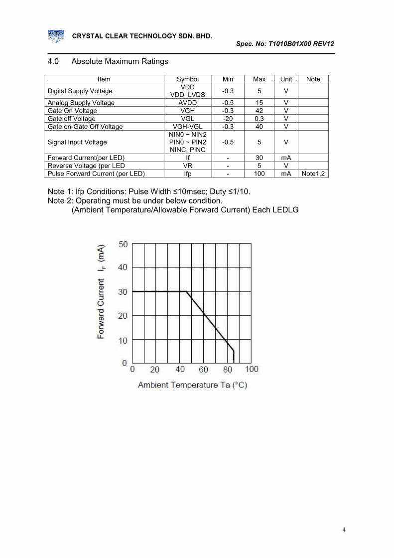
Pulse Forward Current (per LED) Ifp - 100 mA Note1,2
Note 1: Ifp Conditions: Pulse Width ≤10msec; Duty ≤1/10. Note 2: Operating must be under below condition. (Ambient Temperature/Allowable Forward Current) Each LEDLG

CRYSTAL CLEAR TECHNOLOGY SDN. BHD.
Spec. No: T1010B01X00 REV12
5
5.0 Electrical Characteristics
5.1 TFT LCD
ITEM SYMBOL MIN TYP MAX UNIT NOTE
Digital Power Supply Voltage for LCD
DVDD VDD_LVDS
3 3.3 3.6 V
Logic Input Voltage (LVDS:IN+, In-)
VCM [VID]
2 -
2.4 - [VID]
2 V Note 1
[VID] 200 - 600 mV Note 1
VTH - - 100 mV VCM = 1.2V
Note 1
VTL -100 - - mV
Analog Power Supply Voltage
AVDD 9.4 9.6 9.8 V
Gate On Power Supply Voltage
VGH 17 18 19 V
Gate off Power Supply Voltage
VGL -6.6 -6 -5.4 V
Common Power Supply Voltage
VCCOM 3.6 4.0 4.2 V Note2
Gamma Voltage
V1 - 9.02 - V
V2 - 9.01 - V
V3 - 7.62 - V
V4 - 7.15 - V
V5 - 6.85 - V
V6 - 6.52 - V
V7 - 6.46 - V
V8 - 3.58 - V
V9 - 3.5 - V
V10 - 3.1 - V
V11 - 2.76 - V
V12 - 2.23 - V
V13 - 0.67 - V
V14 - 0.63 - V
Note 1: LVDS Signal
(Note2) Suggest to adjust VCOM to an optimum level to minimize flickering effect.

CRYSTAL CLEAR TECHNOLOGY SDN. BHD.
Spec. No: T1010B01X00 REV12
6
5.2 TFT-LCD Current Consumption
ITEM SYMBOL Condition MIN TYPE MAX UNIT NOTE
Gate on power current IVGH VGH =18V - 0.5 1 mA Note1
Gate off power current IVGL VGL= -6V - 0.5 1 mA Note1
Digital power current IVDD VDD = 3.3V - 40 50 mA Note1
Analog power current IAVDD AVDD = 9.6V - 35 45 mA Note1
Total Power Consumption PC - 480 621 mW Note1
Note1: Typical: Under 256 grey pattern Maximum: Under black Pattern
256 grey pattern Black Pattern
5.3 Power Signal sequence
Power On: VDD AVDD/VGL VGH Video & Logic Signal Power Off: Video & Logic Signal VGH AVDD/VGL VDD

CRYSTAL CLEAR TECHNOLOGY SDN. BHD.
Spec. No: T1010B01X00 REV12
7
5.4 Backlight Ta = 25°C
ITEM SYMBOL CONDITIONS MIN TYP MAX UNIT NOTE
LED current IL Ta=25
(30mA/series) -- 390 -- mA
LED voltage VL Ta=25
(30mA/series) 9.2 9.6 9.8 V
LED Lifetime - Ta=25
IF=30mA 35000 Hr
Remarks:
1) LED Circuit Diagram
2) Suggestion: Use constant current control to avoid light leakage phenomenon and uneven
brightness quality issue 3) Definition of lifetime : Luminance < 50% of initial Luminance

CRYSTAL CLEAR TECHNOLOGY SDN. BHD.
Spec. No: T1010B01X00 REV12
8
6.0 Interface Connection
6.1 CN1 (Input Signal)
CRYSTAL CLEAR TECHNOLOGY SDN. BHD.
Spec. No: T1010B01X00 REV12
9
Remarks:
1) Mating Connector : 089K60-000100-G2-R (STARCONN) 2) UPDN and SHLR control function
6.2 Capacitive Touch Panel pin out
PIN SYMBOL
1 VDD 2 GND 3 GND
4 SCL 5 SDA
6 GND
7 INT 8 RST
6.3 CN2 (LED Backlight)
PIN NO SYMBOL FUNCTION
1 A Anode
2 K Cathode
Note: Input Connector: BHSR-02VS-1 (JST) Output Connector: SM02B-BHSS-1 (JST)
46 V7 Gamma correction voltage reference
47 V6 Gamma correction voltage reference
48 V5 Gamma correction voltage reference
49 V4 Gamma correction voltage reference
50 V3 Gamma correction voltage reference
51 V2 Gamma correction voltage reference
52 V1 Gamma correction voltage reference
53 GND Digital ground
54 VDD Digital power
55 SELB 6bit/8bit mode select, SELB = “0”, LVDS input data is 8bits SELB = “1”, LVDS input data is 6bits
56 VGH Positive power for TFT
57 VDD Digital power for Gate IC
58 VGL Negative power for TFT
59 GND Digital ground for Gate IC
60 NC No connection

CRYSTAL CLEAR TECHNOLOGY SDN. BHD.
Spec. No: T1010B01X00 REV12
10
7.0 Input Signal (DE Only Mode) 7.1 Timing Specification
ITEM SYMBOL MIN TYP MAX UNIT
LVDS input signal sequence CLK Frequency tclk 45 51.2 57 MHz
LCD input Signal Sequence (Input LVDS Transmitter)
DENA
Horizontal
Horizontal total Time
tH 1324 1344 1364 tCLK
Horizontal effective Time
tHA
1024
tCLK
Horizontal Blank Time
tHB 300 320 340 tCLK
Vertical
Vertical total Time tV 625 635 645 tH
Vertical effective Time
tVA
600
tH
Vertical Blank Time tVB 25 35 45 tH
7.2 Timing Sequence (Timing Chart)
7.2.2 Vertical Timing Sequence
7.2.1 Horizontal Timing Sequence

CRYSTAL CLEAR TECHNOLOGY SDN. BHD.
Spec. No: T1010B01X00 REV12
11
7.2.3 LVDS Input Data Mapping

12
8.0 Mechanical Specification
(30.3)
226.00 - BEZEL OPENING (MIN)
222.72 A.A
128.50 - BEZEL OPENING (MIN)
125.28 A.A
235.00
143.00
(68.4)
5.76
5.29
(116.65)
(200)
4.5
4.7 WITH FPC
(70.0)
(39.3)
(118.85)
COMPONENT AREA
160
4.0±0.5
P0.5 x (60-1) = 29.5±0.1
160
0.30±0.03
0.50±0.1
30.5±0.1
0.30±0.05
5.50±0.5 - STIFFENER
A
DETAIL A
AGND
1
PIN OUT TABLE
No
Symbol AVND
2
VDD
3
GND
4
VCOM
5
VDD
6
GND
7
V14
8
V13
9
V12
10
V11
11
V10
12
V9
13
V8
14
GND
15
VDD_LVDS
16No
Symbol GND
17
PIND3
18
NIND3
19
GND
20
PINC
21
NINC
22
GND
23
PIND2
24
NIND2
25
GND
26
PIND1
27
NIND1
28
GND
29
PIND0
30
NIND0
31No
Symbol GND
32
GND_LVDS
33
GRB
34
STBYB
35
SHLR
36
VDD
37
UPDN
38
AGND
39
AVDD
40
VCOM
41
DITH
42
GND
43
VDD
44
GND
45
V7
46No
Symbol V6
47
V5
48
V4
49
V3
50
V2
51
V1
52
GND
53
VDD
54
GND
55
VGH
56
VDD
57
VGL
58
GND
59
NC
60
H
1 2 3 4 5 6
G
F
E
C
D
B
A
1 2 3 4 5 6
PART NAME
DRAWING NUMBERCHECKED
7 8
APPROVED
02-11-2015 NTS
UNIT : MM
9
DRAWNSHEET
MECHANICAL
SPECIFICATION
T1010B01N00
10
H11
1
11
REV.
G
F
E
C
D
B
7 8 9 10
A
11
AZHAR
NOTE:
1. GENERAL TOLERANCE ± 0.3mm
2. STORAGE TEMP: -30°C - 70°C
3. OPERATION TEMP: -20°C - 60°C
4. BEZEL: BLACK COATING
5. SYMBOL ( ) INDICATE REFERENCE OR REPEATED DIMENSION
VA Center
1024 (RGB) x 600 dots
224.92 - V.A
127.48 - V.A

13
8 1
VA Center
1024 (RGB) x 600 dots
223.32
247.00
125.88
152.00
74.65
123.50(123.50)
(77.35)
55.42±1.0
65.18
4.50 19.25
DETAIL B
H
1 2 3 4 5 6
G
F
E
C
D
B
A
1 2 3 4 5 6
PART NAME
DRAWING NUMBERCHECKED
7 8
APPROVED
FAISAL23-04-2015 NTS
UNIT : MM
9
DRAWNSHEET
MECHANICAL
SPECIFICATION
T1010B01C00C
10
H41
2
11
REV.
G
F
E
C
D
B
7 8 9 10
A
11
AZHAR23-04-2015
AZHAR23-04-2015
0.300.50
3.50
4.50
0.50
3.50±0.5
R0.30230.0±10.0
0.70 - TOUCH PANEL
0.70 - COVER LENS
4.50 - TFT
6.50±0.5
0.30±0.05
2 SHEET 1/2, 2/2,
CHANGE CTP DESIGN
AZHAR 06-06-2015
CONTACT SIDE STIFFENER
DETAIL B
NOTE:
1. GENERAL TOLERANCE TO BE±0.3
3 SHEET 1/2,
CHANGE WIRE LENGTH
AZHAR 26-08-2015
3
WHITE (A)
BLACK (K)
4 SHEET 1/2,
ADD A AND K INDICATION
AZHAR 26-08-2015
4

14
1 60
4.0±0.5
P0.5 x (60-1) = 29.5±0.1
160
0.30±0.03
0.50±0.1
30.5±0.10.30±0.05
5.50±0.5 - STIFFENER
DETAIL A
H
1 2 3 4 5 6
G
F
E
C
D
B
A
1 2 3 4 5 6
PART NAME
DRAWING NUMBERCHECKED
7 8
APPROVED
FAISAL23-04-2015 NTS
UNIT : MM
9
DRAWNSHEET
MECHANICAL
SPECIFICATION
T1010B01C00C
10
H42
2
11
REV.
G
F
E
C
D
B
7 8 9 10
A
11
AZHAR23-04-2015
AZHAR23-04-2015
DETAIL A
143.0
235.06.9±1.0
2.8±1.0
4.50±1.0
2 SHEET 2/2,
CHANGE CTP DESIGN
AZHAR 06-06-2015
COMPONENT
AREA

CRYSTAL CLEAR TECHNOLOGY SDN. BHD.
Spec. No: T1010B01W01 REV11
15
9.0 Optical Characteristics Ta = 25°C, VCC = 3.3V
Item Symbol Condition Min. Typ. Max Unit
Panel Transmittance T -- 5.5 5.9 -- %
LCM luminance (Center) YL I=140mA 400 450 -- cd/
Response time Rising TR
Point-5 -- 20 40 ms Falling TF
Viewing
Angle
Horizontal f Point-5
CR≧10
120 140 -- 。
Vertical q 100 120 --
Color Filter
Chromaticity White.
X q=Ø﹦0°
0.28 0.30 0.33
Y 0.30 0.32 0.35
Note1: Measuring condition:25±2, 60±10%RH, under 10 Lux luminosity, in a dark room.
Using BM-5A (TOPCON), viewing angle 2°, IL=140 mA (Backlight current measurement is
taken after lighting is switched-on for a duration of 10 min).
Note2: Definition of contrast ratio: Contrast Ratio (CR) = (White) Luminance when pixel is switched ON ÷ (Black) Luminance
when pixel is switched OFF

CRYSTAL CLEAR TECHNOLOGY SDN. BHD.
Spec. No: T1010B01W01 REV11
16
Note3: Definition of luminance:
Measurement of white luminance on point 5 with reference to Figure 9-1. Definition of luminance uniformity:
Measurement of white luminance on point 1~9 with reference to Figure 9-1 and
subjecting the data to the following equation:
L = [L(MIN)/L(MAX)]×100
Fig. 9-1 measuring Point
Note 4: Definition of Viewing Angle (θ,Ψ) refer to Fig 9-2
Fig. 9-2: Definition of Viewing Angle

CRYSTAL CLEAR TECHNOLOGY SDN. BHD.
Spec. No: T1010B01W01 REV11
17
Note 5: Definition of Response Time (White-Black)
10.0 Reliability Test 10.1 Temperature and Humidity
Note 1: Condition of Image Sticking test:25 ± 2 . Operation with sustained
test pattern for 24 hrs, then change to grey pattern immediately. After 5 min, the mural should disappear completely.
Image Sticking-Pattern Grey – Pattern
10.2 Shock and Vibration
TEST ITEMS CONDITIONS NOTE
High Temperature Operation 70 ; 240hrs
High Temperature Storage 80 ; 240hrs
High Temperature High Humidity Operation 60 ; 90%RH ;240hrs No condensation
Low Temperature Operation -20 ; 240hrs Backlight unit always turn on
Low Temperature Storage -30 ; 240hrs
Thermal Shock –30 (0.5hr) ~ 80 (0.5hr) ;
200 Cycles
Image Sticking 40 ; 24hrs Note 1
Luminance
% 90 90 %
10 % t f t
White(63 th )
Black(0) 10 %

CRYSTAL CLEAR TECHNOLOGY SDN. BHD.
Spec. No: T1010B01W01 REV11
18
10.3 Electrostatic Discharge
TEST ITEM CONDITIONS Note
ESD
150pF,330Ω,±8kV&±15kV air& contact test 1
200pF,0Ω,±200V contact test 2
Note: Measure: 1 – LCD glass and metal bezel 2. IF connector pins
10.4 Judgement Standard
The Judgment of the above test should be made as follow:
Pass: Normal display image with no obvious non-uniformity and no line defect.
Partial transformation of the module parts should be ignored.
Fail: No display image, obvious non-uniform display quality.
Notes: 1. If the module is used above these absolute maximum ratings, it may become
permanently damaged. Using the module exceeding the following electrical characteristic conditions, the module will malfunction and cause poor reliability.
2. VCC >VSS must be maintained. 3. Please be sure users are grounded when handing LCD Module.

CRYSTAL CLEAR TECHNOLOGY SDN. BHD.
Spec. No: T1010B01W01 REV11
19
11.0 Precaution for Using TFT Modules
1. Handing Precautions a. The display panel is made of glass and polarizer. As glass is fragile. It tends to chip
during handling especially on the edges. Please avoid dropping or jarring. Do not subject it to a mechanical shock of impact or by dropping it.
b. If the display panel is damaged and the liquid crystal substance leaks out, be sure not to get any in your mouth. If the substance is in contact with your skin or clothes, wash it off using soap and water.
c. Do not apply excessive force to the display surface or the adjoining areas since this may cause the colour tone to vary. Do not touch the display with bare hands. This will stain the display area and degrade the insulation between terminals. Scratch and dents may occur on polarizer too.
d. The polarizer covering the display surface of the LCD module is soft and easily scratched. Handle this polarizer carefully. Do not touch, push or rub the exposed polarizers with anything harder than a HB pencil lead (glass, tweezers, etc.). Do not put or attach anything on the display area to avoid leaving marks on it. Condensation on the surface and contact with terminals due to cold will damage, stain or dirty the polarizer. After products are tested at low temperature they must be warmed up in a container before coming in to contact with room temperature air.
e. If the display surface becomes contaminated, breathe on the surface and gently wipe it with a soft dry cloth. If it is heavily contaminated, moisten cloth with one of the following solvents
- Isopropyl alcohol - Ethyl alcohol - Do not scrub hard to avoid damaging the display surface.
f. Solvents other than those above-mentioned may damage the polarizer. Especially, do not use the following.
- Water - Ketone - Aromatic solvents - Wipe off saliva or water drops immediately, contact with water over a long
period of time may cause deformation or colour fading. Avoid contact with oil and fats.
g. Exercise care to minimize corrosion of the electrode. Corrosion of the electrodes is accelerated by water droplets, moisture condensation or a current flow in a high-humidity environment.
h. Install the LCD Module by using the mounting holes. When mounting the LCD module make sure it is free of twisting, warping and distortion. In particular, do not forcibly pull or bend the I/O cable or the backlight cable.
i. Do not attempt to disassemble or process the LCD module. j. NC terminal should be open. Do not connect anything. k. If the logic circuit power is off, do not apply the input signals. l. Electro-Static Discharge Control. Since this module uses a CMOS LSI, the same
careful attention should be paid to electrostatic discharge as for an ordinary CMOS IC. To prevent destruction of the elements by static electricity, be careful to maintain an optimum work environment.
- Before removing LCM from its packing case or incorporating it into a set, be sure the module and your body have the same electric potential. Be sure to ground the body when handling the LCD modules.
- Tools required for assembly, such as soldering irons, must be properly grounded. Make certain the AC power source for the soldering iron does not leak. When using an electric screwdriver to attach LCM, the screw driver should be of ground potentiality to minimize as much as possible any
CRYSTAL CLEAR TECHNOLOGY SDN. BHD.
Spec. No: T1010B01W01 REV11
20
transmission of electromagnetic waves produced sparks coming from the commutator of the motor.
- To reduce the amount of static electricity generated, do not conduct assembly and other work under dry conditions. To reduce the generation of static electricity be careful that the air in the work environment is not too dry. A relative humidity of 50%-60% is recommended. As far as possible make the electric potential of your work clothes and that of the work bench the ground potential.
- The LCD module is coated with a film to protect the display surface. Exercise care when peeling off this protective film since static electricity may be generated.
m. Since LCM has been assembled and adjusted with a high degree of precision, avoid applying excessive shocks to the module or making any alterations or modifications to it.
- Do not alter, modify or change the shape of the tab on the metal frame. - Do not make extra holes on the printed circuit board, modify its shape or
change the positions of components to be attached. - Do not damage or modify the pattern writing on the printed circuit board. - Absolutely do not modify the zebra rubber strip (conductive rubber) or heat
seal connector. - Except for soldering the interface, do not make any alterations or
modifications with a soldering iron. - Do not drop, bend or twist the LCM.
2. Storage Precautions
When storing the LCD modules, the following precaution are necessary. a. Store them in a sealed polyethylene bag. If properly sealed, there is no need for
the desiccant. b. Store them in a dark place. Do not expose to sunlight or fluorescent light, keep
the temperature between 0C and 35C, and keep the relative humidity between 40%RH and 60%RH.
c. The polarizer surface should not come in contact with any other objects. 3. Others
a. Liquid crystals solidify under low temperature (below the storage temperature range) leading to defective orientation or the generation of air bubbles (black or white). Air bubbles may also be generated if the module is subject to a low temperature.
b. If the LCD modules have been operating for a long time showing the same display patterns, the display patterns may remain on the screen as ghost images and a slight contrast irregularity may also appear. A normal operating status can be regained by suspending use for some time. It should be noted that this phenomenon does not adversely affect performance reliability.
c. To minimize the performance degradation of the LCD modules resulting from destruction caused by static electricity etc. Exercise care to avoid holding the following sections when handling the modules.
Exposed area of the printed circuit board. Terminal electrode sections.
4. Using LCD Modules
a. Installing LCD Modules The hole in the printed circuit board is used to fix LCM as shown in the picture below. Attend to the following items when installing the LCM.

CRYSTAL CLEAR TECHNOLOGY SDN. BHD.
Spec. No: T1010B01W01 REV11
21
b. Cover the surface with a transparent protective plate to protect the polarizer and LC cell.
c. When assembling the LCM into other equipment, the spacer to the bit between the
LCM and the fitting plate should have enough height to avoid causing stress to the module surface, refer to the individual specifications for measurements. The measurement tolerance should be 0.1mm.
d. Precaution for assemble the module with BTB connector: Please note the position of the male and female connector position, don’t assemble or assemble like the method which the following picture shows
5. Precaution for soldering the LCM
Manual soldering Machine drag
soldering Machine press
soldering
No RoHS Product
290°C ~350°C. Time: 3-5S.
330°C ~350°C. Speed: 4-8 mm/s.
300°C ~330°C. Time: 3-6S.
Press: 0.8~1.2Mpa RoHS
Product
340°C ~370°C. Time: 3-5S.
350°C ~370°C. Time: 4-8 mm/s.
330°C ~360°C. Time: 3-6S.
Press: 0.8~1.2Mpa
a. If soldering flux is used, be sure to remove any remaining flux after finishing the soldering operation (This does not apply in the case of a non-halogen type of flux). It is recommended that you protect the LCD surface with a cover during soldering to prevent any damage due to flux spatters.
b. When soldering the electroluminescent panel and PC board, the panel and board should not be detached more than three times. This maximum number is determined by the temperature and time conditions mentioned above, though there may be some variance depending on the temperature of the soldering iron.
c. When removing the electroluminescent panel from the PC board, be sure the solder has completely melted, the soldered pad on the PC board could be damaged.
6. Precautions for Operation
a. Viewing angle varies with the change of liquid crystal driving voltage (VLCD). Adjust VLCD to show the best contrast.
b. It is recommended to drive LCD's within the specified voltage limit since over limit will cause shorter LCD life. An electrochemical reaction due to direct current causes LCD deterioration. Avoid the use of direct current drive.

CRYSTAL CLEAR TECHNOLOGY SDN. BHD.
Spec. No: T1010B01W01 REV11
22
c. Response time will be extremely delayed at lower temperature compared to room operating temperature range and on the other hand, at higher temperature LCD shows dark colour in them. However those phenomena do not mean malfunction. The LCD will return to normal performance when ambient temperature revert to room condition.
d. If the display area is pushed hard during operation, the display will become abnormal. However, it will return to normal if it is turned off and on.
e. A slight dew depositing on terminals is a cause for electro-chemical reaction resulting in terminal open circuit.
f. Input logic voltage before apply analogue high voltage such as LCD driving voltage when power on. Remove analogue high voltage before logic voltage when power off the module. Input each signal after the positive/negative voltage becomes stable.
g. Please keep the temperature within the specified range for use and storage. Polarization degradation, bubble generation or polarizer peel-off may occur with high temperature and high humidity.
7. Safety
a. It is recommended to crush damaged or unnecessary LCDs into pieces and wash them off with solvents such as acetone and ethanol, which should later be burned.
b. If any liquid leaks out of a damaged glass cell and comes in contact with the hands, wash off thoroughly with soap and water.
8. Limited Warranty
Unless otherwise agreed between Crystal Clear Technology and customer, Crystal Clear Technology will replace or repair any of its LCD and LCM which is found to be defective electrically and visually when inspected in accordance with Crystal Clear Technology acceptance standards, for a period of one year from date of shipment. Confirmation of such date shall be based on freight documents. The warranty liability of Crystal Clear Technology is limited to repair and/or replacement on the terms set forth above. Crystal Clear Technology will not responsible for any subsequent or consequential events.
9. Return LCM under Warranty
No warranty can be granted if the precautions stated above have been disregarded. The typical examples of violations are: - Broken LCD glass - PCB eyelet’s damaged or modified - PCB conductors damaged - Circuit modified in any way, including addition of components. - PCB tampered with by grinding, engraving or painting varnish. - Soldering to, or modifying the bezel in any manner. Module repairs will be invoiced to customer upon mutual agreement. Modules must be returned with sufficient description of failure or defects. Any connectors or cable installed by customer must be removed completely without damaging the PCB eyelet’s, conductors and terminals.
.

CRYSTAL CLEAR TECHNOLOGY SDN. BHD.
Spec. No: T1010B01W01 REV11
23
Attachment 1.
Capacitive Touch Panel Specification

CRYSTAL CLEAR TECHNOLOGY SDN. BHD.
Spec. No: T1010B01W01 REV11
24
Contents
1. General Specification
2. Electrical Characteristics
3. Optical Characteristics
4. Reliability
5. Durability
6. Touch panel description
6.1 Block diagram
6.2 Touch panel pin assignment
7. Appearance Inspection
7.1 Inspection Conditions
7.2 Appearance Standard

CRYSTAL CLEAR TECHNOLOGY SDN. BHD.
Spec. No: T1010B01W01 REV11
25
1. General Specification
Item CONTENTS Unit
Outline Dimension 247*152 mm
Active Area(W*L) 224.32*126.88 mm
View Area 223.32*125.88 mm
TP size (inch) 10.1 inch
Controller IC FT5426
Interface Type IIC -
I2C Slave Address 0X38
Number of touch point 1024x600(5Point) Dot
Number of button -- -
Operation Temperature TOPL = -20, TOPH =70
Storage Temperature TSTL = -30, TSTH =80
ITO Glass thickness ITO 0.7 mm
Cover lens thickness 0.7 mm
Resolution >100 dpi
Input force <10g
Surface hardness >6H
2. Electrical Characteristics (Ta====25 )
Item Symbol Condition Min. Type Max. Unit
Power Supply VCC -- 2.8 3.3 3.5 Volt
Supply Current
IDD
Vcc =3.3V Free mode - 16.5 35 mA
Vcc =3.3V watch mode - 16.5 35 mA
Vcc =3.3V Active mode - 18.5 40 mA
Vcc =3.3V Fast mode - 18.5 40 mA

CRYSTAL CLEAR TECHNOLOGY SDN. BHD.
Spec. No: T1010B01W01 REV11
26
3. Optical Characteristics
Item CONTENTS Remark
Transparency >87%
4. Reliability
No.1 Test Items Test Condition Remark
1 High Temperature Storage Test Ta= 70 240 hours (1),(2)
2 Low Temperature Storage Test Ta= -30 240 hours (1),(2)
3 High Temperature Operation Test
Ta= 70 24 hours (1),(2)
4 Low Temperature Operation Test Ta= -20 24 hours (1),(2)
5 High Temperature and High Humidity Operation Test
Ta=60 90%RH 240 hours (Without dewing)
(1),(2)
6 Thermal Shock Test (non-operating)
-20(30min) ~ 70(30min), 10 cycles
(1),(2)
Note: (1) After the reliability test, the product should work functionally. (2)Before visual and function test, the product should be given at least 2 hours
at room temperature to normalize. 6. Touch panel description
6.1 Block diagram

CRYSTAL CLEAR TECHNOLOGY SDN. BHD.
Spec. No: T1010B01W01 REV11
27
6.2 Touch panel pin assignment
7. Appearance Inspection
7.1 Conditions and methods of appearance inspection
7.1.1 Inspection distance:25~30cm
7.1.2 From lamp source to product:250cm
7.1.3 Angle of inspection: Ambient brightness 1k-1.5k lux inspection from front view, perpendicular to the surface of product.
7.1.4 For pin hole defect is determined by the size of D dot diameter, irregular dot defect is determined by D= (length + width)/2.
D=(a+b)/2
Pin Symbol Description
1 VDD Power supply
2 GND Power ground.
3 GND Power ground.
4 SCL IIC clock signal. Must be pulled high.
5 SDA IIC data signal. Must be pulled high.
6 GND Power ground.
7 INT External interrupt to the host
8 RST External Reset, Low is active
CRYSTAL CLEAR TECHNOLOGY SDN. BHD.
Spec. No: T1010B01W01 REV11
28
7.2 Products appearance standard:
Defect
Description 10.1""""TP standard
Defects
classification urge
MA MI
Corner chip
X≤1.0mm; Y≤1.0mm;Z1/2T;
unilateral allowed 1
OK
X>1.0mm, Y>1.0mm
NG
Edge chip
X≤1.0mm; Y≤1.0mm,Z1/2T;
unilateral allowed 1
OK
X>1.0mm, Y>1.0mm
NG
1. Touch sensor corner and edge chip that do not
cause any damage to tracer and not visible to end-
user after housing assembly.
2. Lens edge and corner chip that is not visible to
end-user after housing assembly.
OK
Sensor surface edge/corner breakage damage
circuit and visible from front view
NG
Glass
crack
Any crack
NG
Line shape (including scratch fiber)
W:width L:length
W ≤0.03mm,ignore
OK
0.05 mm≤W≤0.1 mm, L ≤3mm,allowed two lines,
distance should above 10mm
OK
W>0.1mm,L>3mm
NG

CRYSTAL CLEAR TECHNOLOGY SDN. BHD.
Spec. No: T1010B01W01 REV11
29
Foreign
round shape
(e.g.
white dot,
black dot,
air bubble) D
= diameter
D≤0.15 mm,ignore, the whole surface and dense
dots not allowed.
OK
0.15 mm<D≤0.25 mm,allowed two dots, distance
should be above 10mm
O
K
D>0.25mm NG
Dent
D≤0.15 mm,ignore, the whole surface and dense
dots not allowed. OK
0.15 mm<D≤0.25mm, allowed two dots, distance
should be above 10mm.
OK
D>0.25mm
NG
Printing ink light leakage
Light leakage at marginal area width ≤0.15mm
OK
Light leakage at marginal area, width >0.15mm NG
Surface
smudginess
For those that can be cleaned, ≤20% of inspected
quantity in one lot under > class 10K area; ≤10%
of inspected quantity in one lot ≤ class 10K area
OK
For those that cannot be cleaned it is classified as
foreign round shape defect
OK

CRYSTAL CLEAR TECHNOLOGY SDN. BHD.
Spec. No: T1010B01W01 REV11
30
FPC defects
on contact
pad
Dent, pinhole a≤w/3
OK
Open circuit /cracking NG
Oxidation, contamination NG
FPC broken
FPC broken /extruded NG
FPC warped
FPC warped
OK