processor design - 2 - kfupmfaculty.kfupm.edu.sa/.../core/chapter5.2-processor_design.pdf ·...
TRANSCRIPT
Chapter 5.2 - Processor Design 21
Processor Design - 2
Computer Architecture
Chapter 5.2 - Processor Design 22
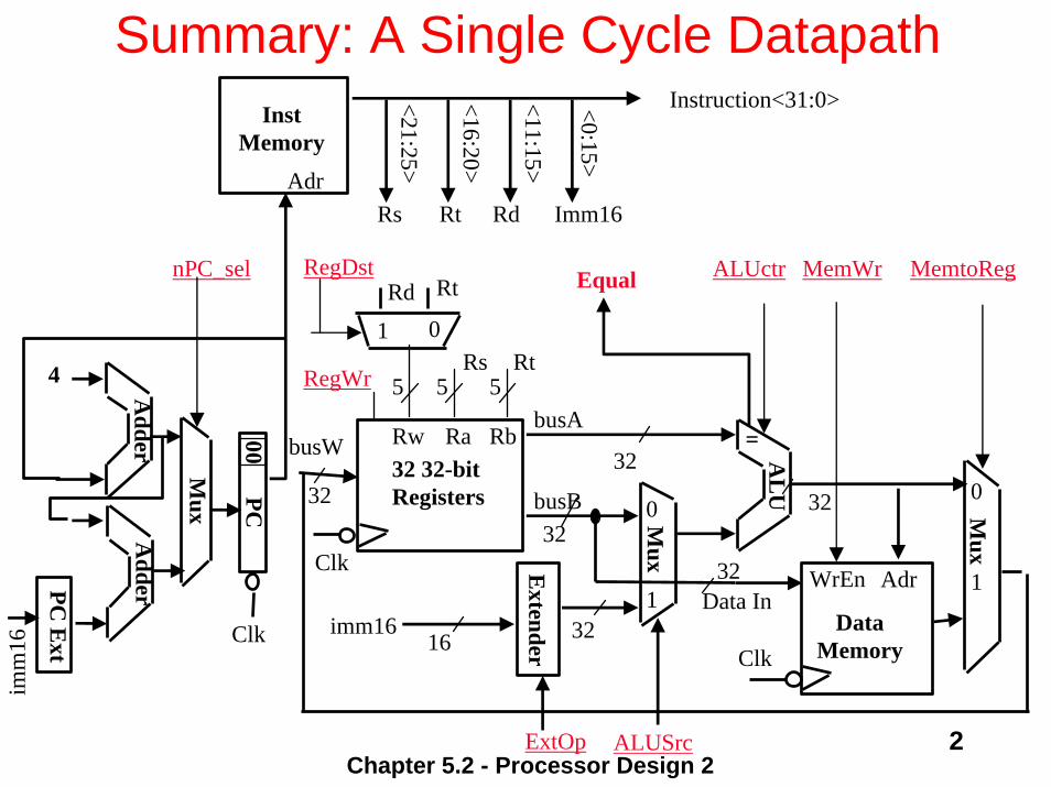
Summary: A Single Cycle Datapathim
m16
32
ALUctr
Clk
busW
RegWr
3232
busA
32busB
55 5
Rw Ra Rb32 32-bitRegisters
Rs
Rt
Rt
RdRegDst
Extender
Mux
3216imm16
ALUSrcExtOp
Mux
MemtoReg
Clk
Data InWrEn32 Adr
DataMemory
MemWrA
LU
Equal
Instruction<31:0>
0
1
0
1
01
<21:25>
<16:20>
<11:15>
<0:15>
Imm16RdRtRs
=
Adder
Adder
PC
Clk
00Mux
4
nPC_sel
PC E
xt
Adr
InstMemory
Chapter 5.2 - Processor Design 23
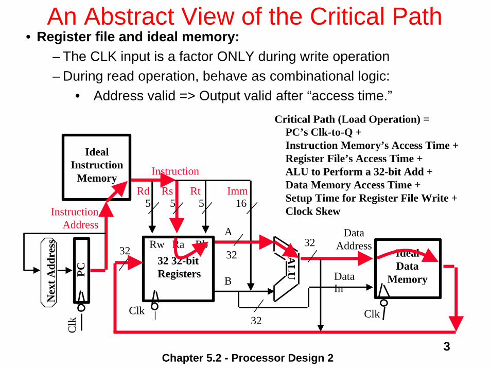
An Abstract View of the Critical Path• Register file and ideal memory:
– The CLK input is a factor ONLY during write operation– During read operation, behave as combinational logic:
• Address valid => Output valid after “access time.”Critical Path (Load Operation) =
PC’s Clk-to-Q +Instruction Memory’s Access Time +Register File’s Access Time +ALU to Perform a 32-bit Add +Data Memory Access Time +Setup Time for Register File Write +Clock Skew
Clk
5
Rw Ra Rb32 32-bitRegisters
RdA
LU
Clk
Data In
DataAddress
IdealData
Memory
Instruction
InstructionAddress
IdealInstruction
Memory
Clk
PC
5Rs
5Rt
16Imm
32
323232
A
B
Nex
t Add
ress
Chapter 5.2 - Processor Design 24
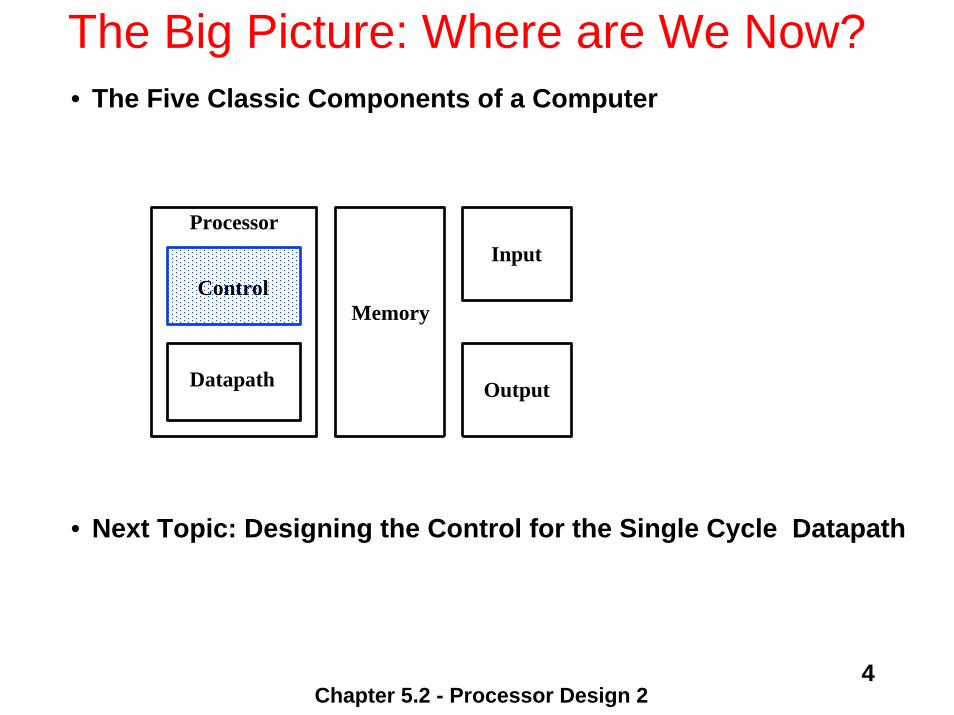
The Big Picture: Where are We Now? • The Five Classic Components of a Computer
• Next Topic: Designing the Control for the Single Cycle Datapath
Control
Datapath
Processor
Memory
Input
Output
Chapter 5.2 - Processor Design 25
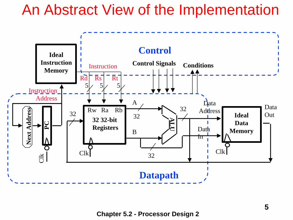
An Abstract View of the Implementation
DataOut
Clk
5
Rw Ra Rb32 32-bitRegisters
Rd
AL
U
Clk
Data In
DataAddress
IdealData
Memory
Instruction
InstructionAddress
IdealInstruction
Memory
Clk
PC
5Rs
5Rt
32
323232
A
B
Nex
t Add
ress
Control
Datapath
Control Signals Conditions
Chapter 5.2 - Processor Design 26
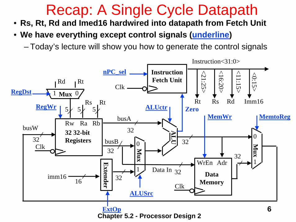
Recap: A Single Cycle Datapath• Rs, Rt, Rd and Imed16 hardwired into datapath from Fetch Unit• We have everything except control signals (underline)
– Today’s lecture will show you how to generate the control signals
32
ALUctr
Clk
busW
RegWr
3232
busA
32busB
55 5
Rw Ra Rb32 32-bitRegisters
Rs
Rt
Rt
RdRegDst
Extender
Mux
Mux
3216imm16
ALUSrc
ExtOp
Mux
MemtoReg
Clk
Data InWrEn
32Adr
DataMemory
32
MemWrA
LU
InstructionFetch Unit
Clk
Zero
Instruction<31:0>
0
1
0
1
01<21:25>
<16:20>
<11:15>
<0:15>
Imm16RdRsRt
nPC_sel
Chapter 5.2 - Processor Design 27
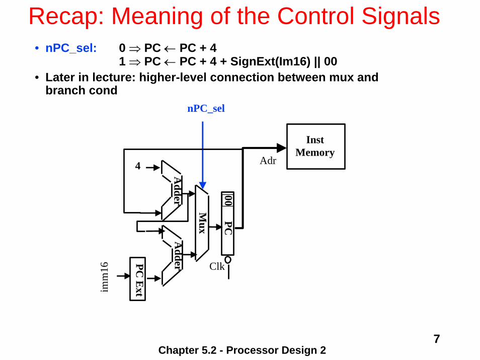
Recap: Meaning of the Control Signals• nPC_sel: 0 ⇒ PC ← PC + 4
1 ⇒ PC ← PC + 4 + SignExt(Im16) || 00• Later in lecture: higher-level connection between mux and
branch cond
Adr
InstMemory
Adder
Adder
PCClk
00Mux
4
nPC_sel
PC E
xtimm
16
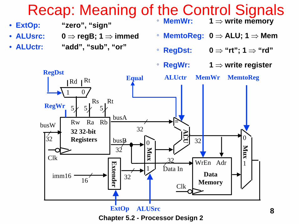
Recap: Meaning of the Control Signals“zero”, “sign”0 ⇒ regB; 1 ⇒ immed“add”, “sub”, “or”
° MemWr: 1 ⇒ write memory
° MemtoReg: 0 ⇒ ALU; 1 ⇒ Mem
° RegDst: 0 ⇒ “rt”; 1 ⇒ “rd”
° RegWr: 1 ⇒ write register
• ExtOp:• ALUsrc:• ALUctr:
Chapter 5.2 - Processor Design 28
32
ALUctr
Clk
busW
RegWr
3232
busA
32busB
55 5
Rw Ra Rb32 32-bitRegisters
Rs
Rt
Rt
RdRegDst
Extender
Mux
3216imm16
ALUSrcExtOp
Mux
MemtoReg
Clk
Data InWrEn32 Adr
DataMemory
MemWr
AL
U
Equal
0
1
0
1
01
=
Chapter 5.2 - Processor Design 29
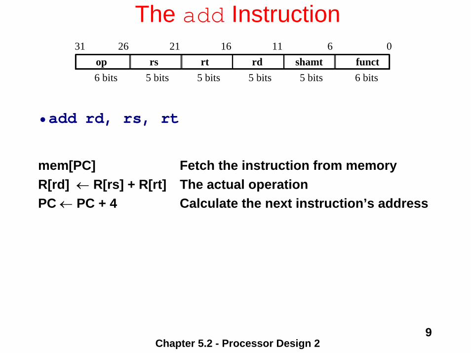
The add Instruction
op rs rt rd shamt funct061116212631
6 bits 6 bits5 bits5 bits5 bits5 bits
•add rd, rs, rt
mem[PC] Fetch the instruction from memoryR[rd] ← R[rs] + R[rt] The actual operationPC ← PC + 4 Calculate the next instruction’s address
Chapter 5.2 - Processor Design 210
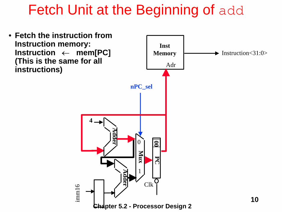
Fetch Unit at the Beginning of add
• Fetch the instruction from Instruction memory: Instruction ← mem[PC] (This is the same for all instructions) Adr
InstMemory
Adder
Adder
PC
Clk
00Mux
4
nPC_selim
m16
Instruction<31:0>
0
1

Chapter 5.2 - Processor Design 211
The Single Cycle Datapath during addop rs rt rd shamt funct
061116212631
• R[rd] ← R[rs] + R[rt]
32
ALUctr = Add
Clk
busW
RegWr = 1
3232
busA
32busB
55 5
Rw Ra Rb32 32-bitRegisters
Rs
Rt
Rt
RdRegDst = 1
Extender
Mux
Mux
3216imm16
ALUSrc = 0
ExtOp = x
Mux
MemtoReg = 0
Clk
Data InWrEn
32Adr
DataMemory
32
MemWr = 0A
LU
InstructionFetch Unit
Clk
Zero
Instruction<31:0>
0
1
0
1
01<21:25>
<16:20>
<11:15>
<0:15>
Imm16RdRsRt
nPC_sel= +4
Chapter 5.2 - Processor Design 212
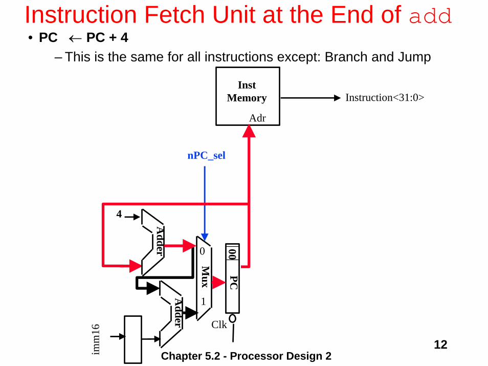
Instruction Fetch Unit at the End of add• PC ← PC + 4
– This is the same for all instructions except: Branch and Jump
Adr
InstMemory
Adder
Adder
PC
Clk
00Mux
4
nPC_sel
imm
16Instruction<31:0>
0
1
Chapter 5.2 - Processor Design 213
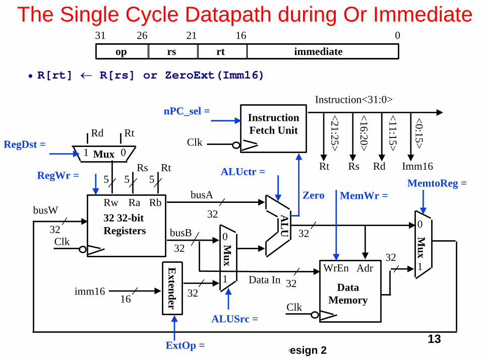
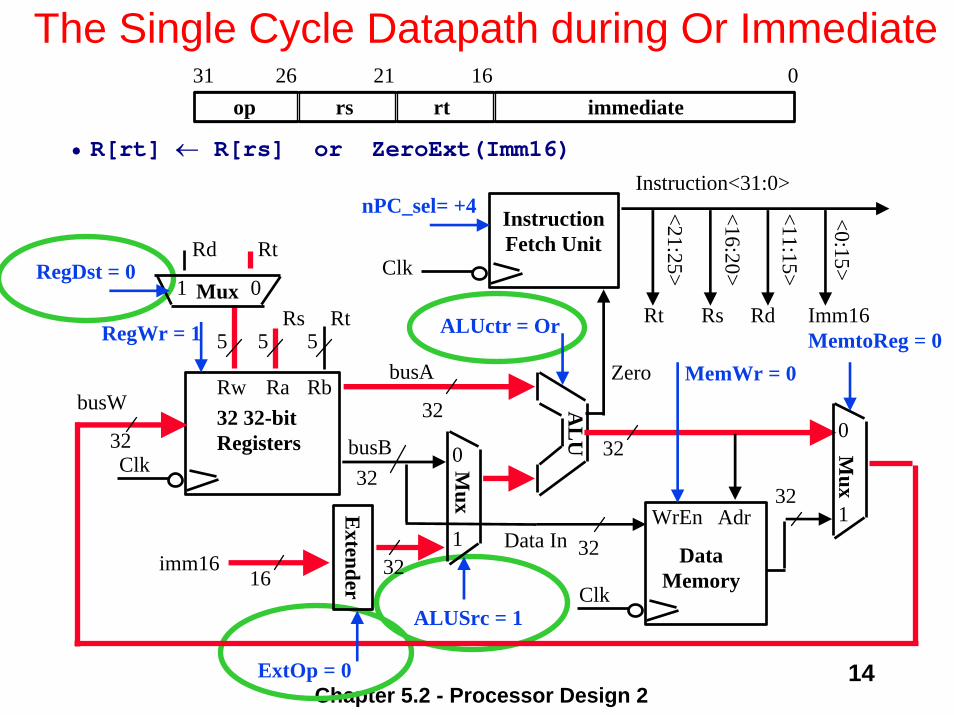
The Single Cycle Datapath during Or Immediateop rs rt immediate
016212631
• R[rt] ← R[rs] or ZeroExt(Imm16)
32
ALUctr =
Clk
busW
RegWr =
3232
busA
32busB
55 5
Rw Ra Rb32 32-bitRegisters
Rs
Rt
Rt
RdRegDst =
Extender
Mux
Mux
3216imm16
ALUSrc =
ExtOp =
Mux
MemtoReg =
Clk
Data InWrEn
32Adr
DataMemory
32
MemWr = A
LU
InstructionFetch Unit
Clk
Zero
Instruction<31:0>
0
1
0
1
01<21:25>
<16:20>
<11:15>
<0:15>
Imm16RdRsRt
nPC_sel =
Chapter 5.2 - Processor Design 214
The Single Cycle Datapath during Or Immediate
op rs rt immediate016212631
• R[rt] ← R[rs] or ZeroExt(Imm16)
32
ALUctr = Or
Clk
busW
RegWr = 1
3232
busA
32busB
55 5
Rw Ra Rb32 32-bitRegisters
Rs
Rt
Rt
RdRegDst = 0
Extender
Mux
Mux
3216imm16
ALUSrc = 1
ExtOp = 0
Mux
MemtoReg = 0
Clk
Data InWrEn
32Adr
DataMemory
32
MemWr = 0A
LU
InstructionFetch Unit
Clk
Zero
Instruction<31:0>
0
1
0
1
01<21:25>
<16:20>
<11:15>
<0:15>
Imm16RdRsRt
nPC_sel= +4

Chapter 5.2 - Processor Design 215
The Single Cycle Datapath during Loadop rs rt immediate
016212631
• R[rt] ← Data Memory {R[rs] + SignExt[imm16]}
32
ALUctr = Add
Clk
busW
RegWr = 1
3232
busA
32busB
55 5
Rw Ra Rb32 32-bitRegisters
Rs
Rt
Rt
RdRegDst = 0
Extender
Mux
Mux
3216imm16
ALUSrc = 1
ExtOp = 1
Mux
MemtoReg = 1
Clk
Data InWrEn
32Adr
DataMemory
32
MemWr = 0A
LU
InstructionFetch Unit
Clk
Zero
Instruction<31:0>
0
1
0
1
01<21:25>
<16:20>
<11:15>
<0:15>
Imm16RdRsRt
nPC_sel= +4

Chapter 5.2 - Processor Design 216
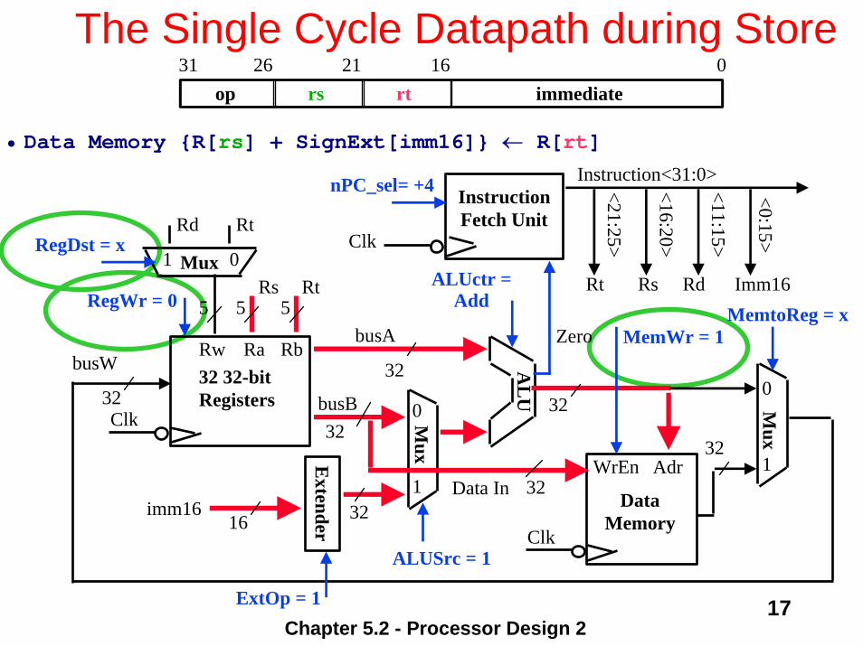
The Single Cycle Datapath during Storeop rs rt immediate
016212631
• Data Memory {R[rs] + SignExt[imm16]} ← R[rt]
32
ALUctr =
Clk
busW
RegWr =
3232
busA
32busB
55 5
Rw Ra Rb32 32-bitRegisters
Rs
Rt
Rt
RdRegDst =
Extender
Mux
Mux
3216imm16
ALUSrc =
ExtOp =
Mux
MemtoReg =
Clk
Data InWrEn
32Adr
DataMemory
32
MemWr = A
LU
InstructionFetch Unit
Clk
Zero
Instruction<31:0>
0
1
0
1
01<21:25>
<16:20>
<11:15>
<0:15>
Imm16RdRsRt
nPC_sel =
Chapter 5.2 - Processor Design 217
The Single Cycle Datapath during Storeop rs rt immediate
016212631
• Data Memory {R[rs] + SignExt[imm16]} ← R[rt]
Instruction<31:0>
32
ALUctr = Add
Clk
busW
RegWr = 0
3232
busA
32busB
55 5
Rw Ra Rb32 32-bitRegisters
Rs
Rt
Rt
RdRegDst = x
Extender
Mux
Mux
3216imm16
ALUSrc = 1
ExtOp = 1
Mux
MemtoReg = x
Clk
Data InWrEn
32Adr
DataMemory
32
MemWr = 1A
LU
InstructionFetch Unit
Clk
Zero
0
1
0
1
01<21:25>
<16:20>
<11:15>
<0:15>
Imm16RdRsRt
nPC_sel= +4
Chapter 5.2 - Processor Design 218
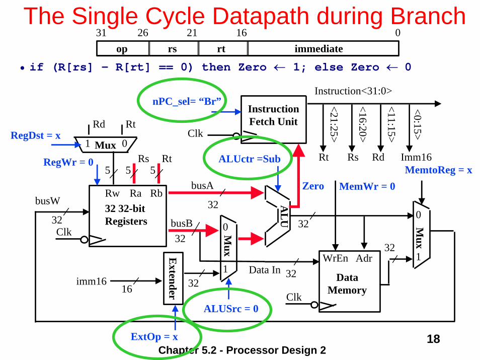
The Single Cycle Datapath during Branch
• if (R[rs] – R[rt] == 0) then Zero ← 1; else Zero ← 0
op rs rt immediate016212631
32
ALUctr =Sub
Clk
busW
RegWr = 0
3232
busA
32busB
55 5
Rw Ra Rb32 32-bitRegisters
Rs
Rt
Rt
RdRegDst = x
Extender
Mux
Mux
3216imm16
ALUSrc = 0
ExtOp = x
Mux
MemtoReg = x
Clk
Data InWrEn
32Adr
DataMemory
32
MemWr = 0A
LU
InstructionFetch Unit
Clk
Zero
Instruction<31:0>
0
1
0
1
01<21:25>
<16:20>
<11:15>
<0:15>
Imm16RdRsRt
nPC_sel= “Br”
Chapter 5.2 - Processor Design 219
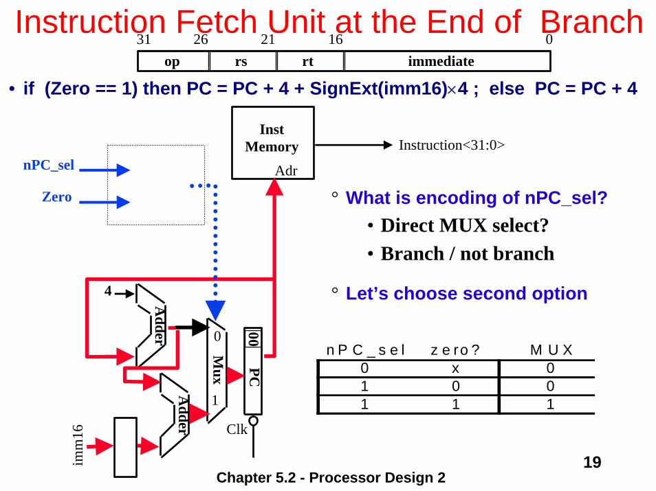
Instruction Fetch Unit at the End of Branch
• if (Zero == 1) then PC = PC + 4 + SignExt(imm16)×4 ; else PC = PC + 4op rs rt immediate
016212631
° What is encoding of nPC_sel?• Direct MUX select?• Branch / not branch
° Let’s choose second option
n P C _ s e l z e ro ? M U X0 x 01 0 01 1 1
Adr
InstMemory
Adder
Adder
PC
Clk
00Mux
4
nPC_sel
imm
16
Instruction<31:0>
0
1
Zero
Chapter 5.2 - Processor Design 220
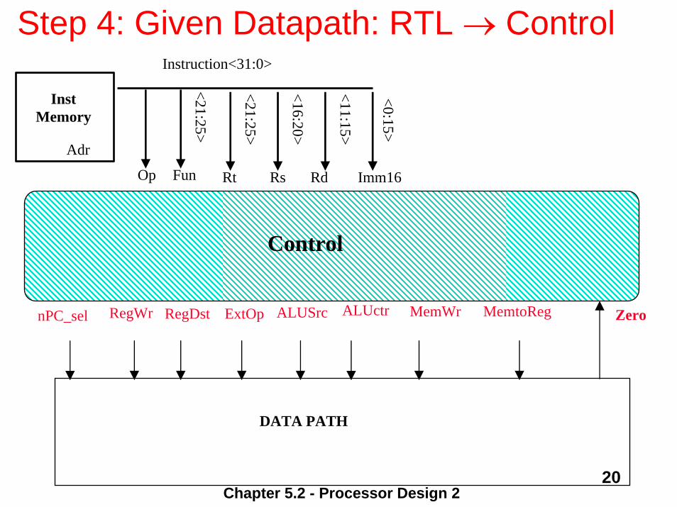
Step 4: Given Datapath: RTL → Control
ALUctrRegDst ALUSrcExtOp MemtoRegMemWr Zero
Instruction<31:0>
<21:25>
<16:20>
<11:15>
<0:15>
Imm16RdRsRt
nPC_sel
Adr
InstMemory
DATA PATH
Control
Op
<21:25>
Fun
RegWr
Chapter 5.2 - Processor Design 221
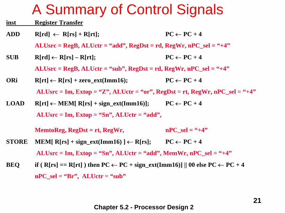
A Summary of Control Signalsinst Register Transfer
ADD R[rd] ← R[rs] + R[rt]; PC ← PC + 4
ALUsrc = RegB, ALUctr = “add”, RegDst = rd, RegWr, nPC_sel = “+4”
SUB R[rd] ← R[rs] – R[rt]; PC ← PC + 4
ALUsrc = RegB, ALUctr = “sub”, RegDst = rd, RegWr, nPC_sel = “+4”
ORi R[rt] ← R[rs] + zero_ext(Imm16); PC ← PC + 4
ALUsrc = Im, Extop = “Z”, ALUctr = “or”, RegDst = rt, RegWr, nPC_sel = “+4”
LOAD R[rt] ← MEM[ R[rs] + sign_ext(Imm16)]; PC ← PC + 4
ALUsrc = Im, Extop = “Sn”, ALUctr = “add”,
MemtoReg, RegDst = rt, RegWr, nPC_sel = “+4”
STORE MEM[ R[rs] + sign_ext(Imm16) ] ← R[rs]; PC ← PC + 4
ALUsrc = Im, Extop = “Sn”, ALUctr = “add”, MemWr, nPC_sel = “+4”
BEQ if ( R[rs] == R[rt] ) then PC ← PC + sign_ext(Imm16)] || 00 else PC ← PC + 4
nPC_sel = “Br”, ALUctr = “sub”
Chapter 5.2 - Processor Design 222
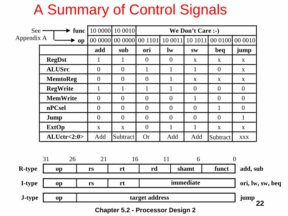
A Summary of Control Signals
add sub ori lw sw beq jumpRegDstALUSrcMemtoRegRegWriteMemWritenPCselJumpExtOpALUctr<2:0>
1001000x
Add
1001000x
Subtract
01010000
Or
01110001
Add
x1x01001
Add
x0x0010x
Subtract
xxx0001x
xxx
funcop 00 0000 00 0000 00 1101 10 0011 10 1011 00 0100 00 0010Appendix A
10 0000See 10 0010 We Don’t Care :-)
op target address
op rs rt rd shamt funct061116212631
op rs rt immediate
R-type
I-type
J-type
add, sub
ori, lw, sw, beq
jump
Chapter 5.2 - Processor Design 223
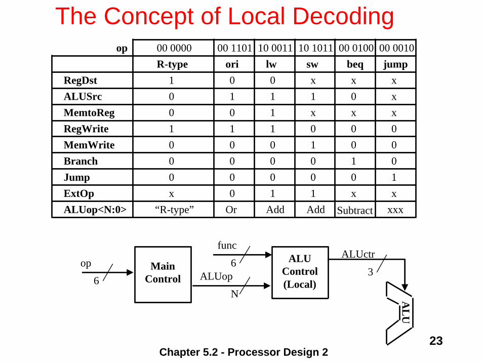
The Concept of Local Decoding
R-type ori lw sw beq jumpRegDstALUSrcMemtoRegRegWriteMemWriteBranchJumpExtOpALUop<N:0>
1001000x
“R-type”
01010000
Or
01110001
Add
x1x01001
Add
x0x0010x
Subtract
xxx0001x
xxx
op 00 0000 00 1101 10 0011 10 1011 00 0100 00 0010
MainControl
op6
ALUControl(Local)
func
N
6ALUop
ALUctr
3
AL
U
Chapter 5.2 - Processor Design 224
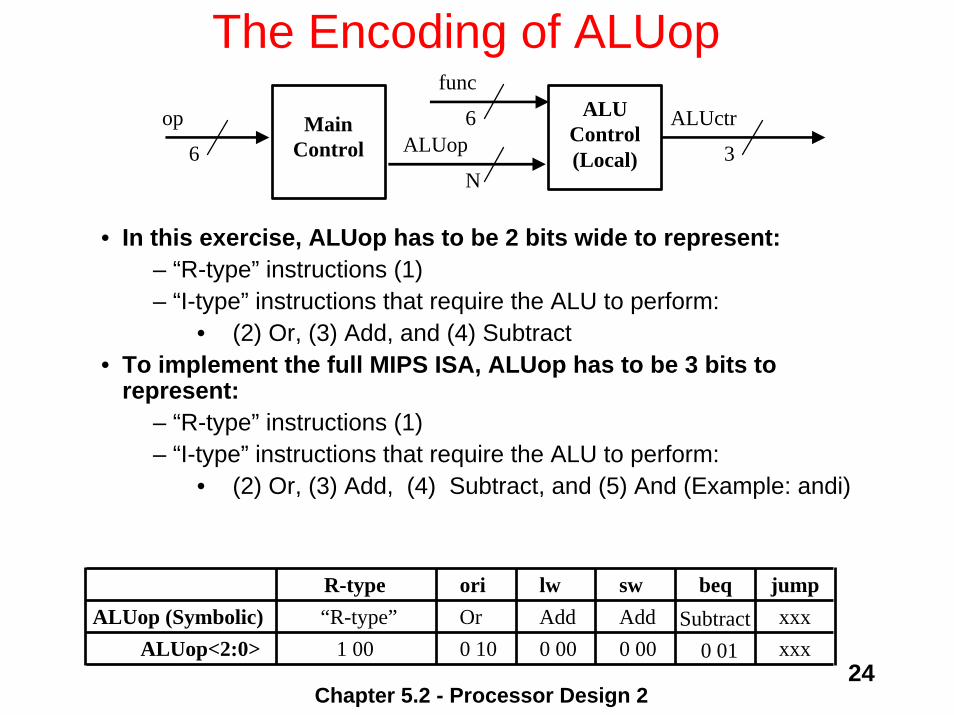
The Encoding of ALUop
MainControl
op
6
ALUControl(Local)
func
N
6ALUop
ALUctr
3
• In this exercise, ALUop has to be 2 bits wide to represent:– “R-type” instructions (1) – “I-type” instructions that require the ALU to perform:
• (2) Or, (3) Add, and (4) Subtract• To implement the full MIPS ISA, ALUop has to be 3 bits to
represent:– “R-type” instructions (1) – “I-type” instructions that require the ALU to perform:
• (2) Or, (3) Add, (4) Subtract, and (5) And (Example: andi)
R-type ori lw sw beq jumpALUop (Symbolic) “R-type” Or Add Add Subtract xxx
ALUop<2:0> 1 00 0 10 0 00 0 00 0 01 xxx
Chapter 5.2 - Processor Design 225
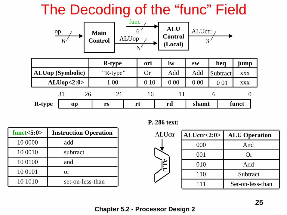
The Decoding of the “func” FieldMain
Controlop
6
ALUControl(Local)
func
N
6ALUop
ALUctr3
R-type ori lw sw beq jumpALUop (Symbolic) “R-type” Or Add Add Subtract xxx
ALUop<2:0> 1 00 0 10 0 00 0 00 0 01 xxx
op rs rt rd shamt funct061116212631
R-type
funct<5:0> Instruction Operation10 000010 001010 010010 010110 1010
addsubtractandorset-on-less-than
ALUctr<2:0> ALU Operation000001010110111
AndOr
AddSubtract
Set-on-less-than
P. 286 text:
ALUctr
AL
U
Chapter 5.2 - Processor Design 226
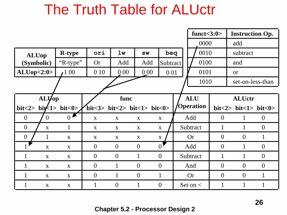
The Truth Table for ALUctr
R-type ori lw sw beqALUop(Symbolic) “R-type” Or Add Add Subtract
ALUop<2:0> 1 00 0 10 0 00 0 00 0 01
ALUop funcbit<2> bit<1> bit<0> bit<2> bit<1> bit<0>bit<3>
0 0 0 x x x x
ALUctrALUOperation
Add 0 1 0bit<2> bit<1> bit<0>
0 x 1 x x x x Subtract 1 1 00 1 x x x x x Or 0 0 11 x x 0 0 0 0 Add 0 1 01 x x 0 0 1 0 Subtract 1 1 01 x x 0 1 0 0 And 0 0 01 x x 0 1 0 1 Or 0 0 11 x x 1 0 1 0 Set on < 1 1 1
funct<3:0> Instruction Op.00000010010001011010
addsubtractandorset-on-less-than
Chapter 5.2 - Processor Design 227
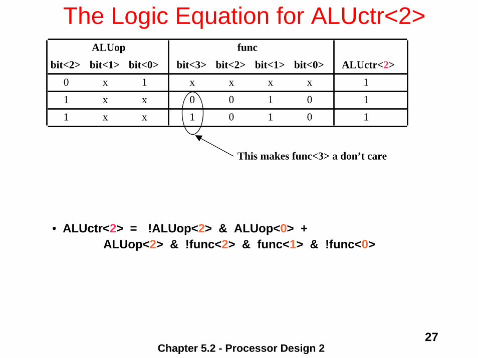
The Logic Equation for ALUctr<2>ALUop func
bit<2> bit<1> bit<0> bit<2> bit<1> bit<0>bit<3> ALUctr<2>0 x 1 x x x x 11 x x 0 0 1 0 11 x x 1 0 1 0 1
This makes func<3> a don’t care
• ALUctr<2> = !ALUop<2> & ALUop<0> +ALUop<2> & !func<2> & func<1> & !func<0>
Chapter 5.2 - Processor Design 228
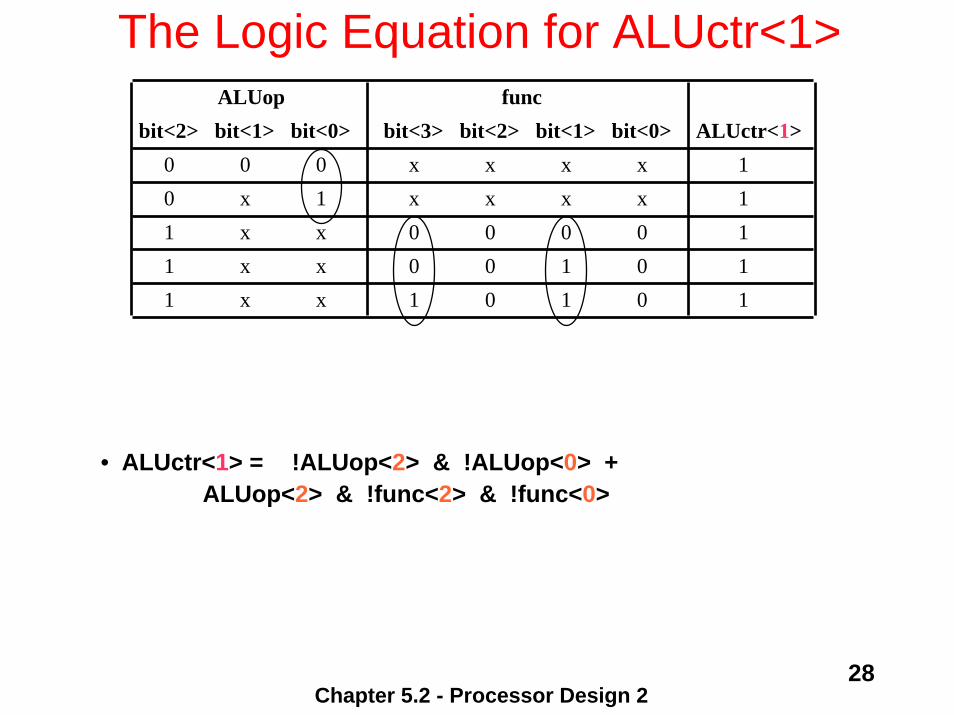
The Logic Equation for ALUctr<1>ALUop func
bit<2> bit<1> bit<0> bit<2> bit<1> bit<0>bit<3>0 0 0 x x x x 1
ALUctr<1>
0 x 1 x x x x 11 x x 0 0 0 0 11 x x 0 0 1 0 11 x x 1 0 1 0 1
• ALUctr<1> = !ALUop<2> & !ALUop<0> +ALUop<2> & !func<2> & !func<0>
Chapter 5.2 - Processor Design 229
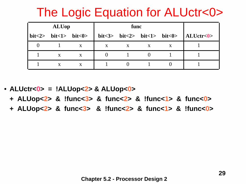
The Logic Equation for ALUctr<0>ALUop func
bit<2> bit<1> bit<0> bit<2> bit<1> bit<0>bit<3> ALUctr<0>
0 1 x x x x x 1
1 x x 0 1 0 1 1
1 x x 1 0 1 0 1
• ALUctr<0> = !ALUop<2> & ALUop<0>+ ALUop<2> & !func<3> & func<2> & !func<1> & func<0>+ ALUop<2> & func<3> & !func<2> & func<1> & !func<0>
Chapter 5.2 - Processor Design 230
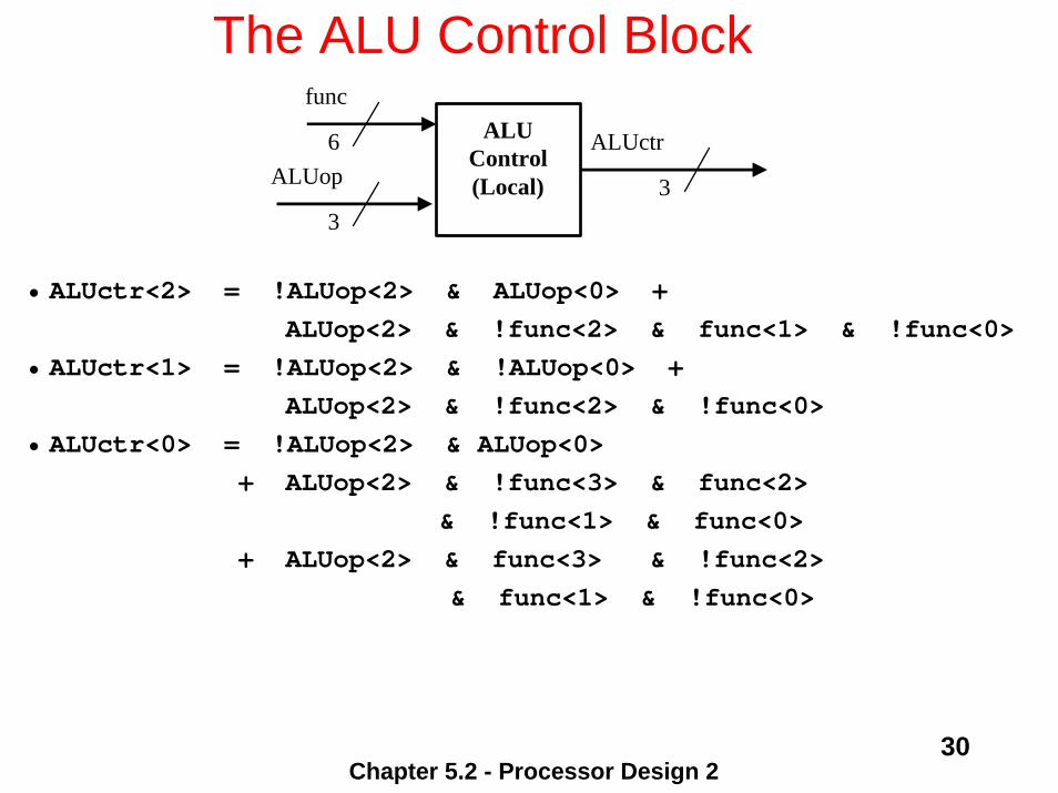
The ALU Control BlockALU
Control(Local)
func
3
6ALUop
ALUctr
3
• ALUctr<2> = !ALUop<2> & ALUop<0> +ALUop<2> & !func<2> & func<1> & !func<0>
• ALUctr<1> = !ALUop<2> & !ALUop<0> +ALUop<2> & !func<2> & !func<0>
• ALUctr<0> = !ALUop<2> & ALUop<0>+ ALUop<2> & !func<3> & func<2>
& !func<1> & func<0>+ ALUop<2> & func<3> & !func<2>
& func<1> & !func<0>
Chapter 5.2 - Processor Design 231
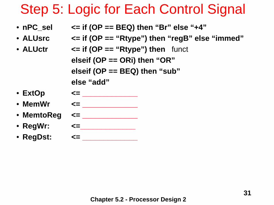
Step 5: Logic for Each Control Signal• nPC_sel <= if (OP == BEQ) then “Br” else “+4”• ALUsrc <= if (OP == “Rtype”) then “regB” else “immed”• ALUctr <= if (OP == “Rtype”) then funct
elseif (OP == ORi) then “OR”elseif (OP == BEQ) then “sub”else “add”
• ExtOp <= _____________• MemWr <= _____________• MemtoReg <= _____________• RegWr: <=_____________• RegDst: <= _____________
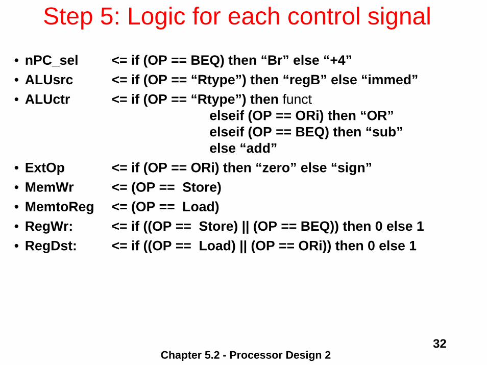
Chapter 5.2 - Processor Design 232
Step 5: Logic for each control signal• nPC_sel <= if (OP == BEQ) then “Br” else “+4”• ALUsrc <= if (OP == “Rtype”) then “regB” else “immed”• ALUctr <= if (OP == “Rtype”) then funct
elseif (OP == ORi) then “OR”elseif (OP == BEQ) then “sub”else “add”
• ExtOp <= if (OP == ORi) then “zero” else “sign”• MemWr <= (OP == Store)• MemtoReg <= (OP == Load)• RegWr: <= if ((OP == Store) || (OP == BEQ)) then 0 else 1• RegDst: <= if ((OP == Load) || (OP == ORi)) then 0 else 1
Chapter 5.2 - Processor Design 233
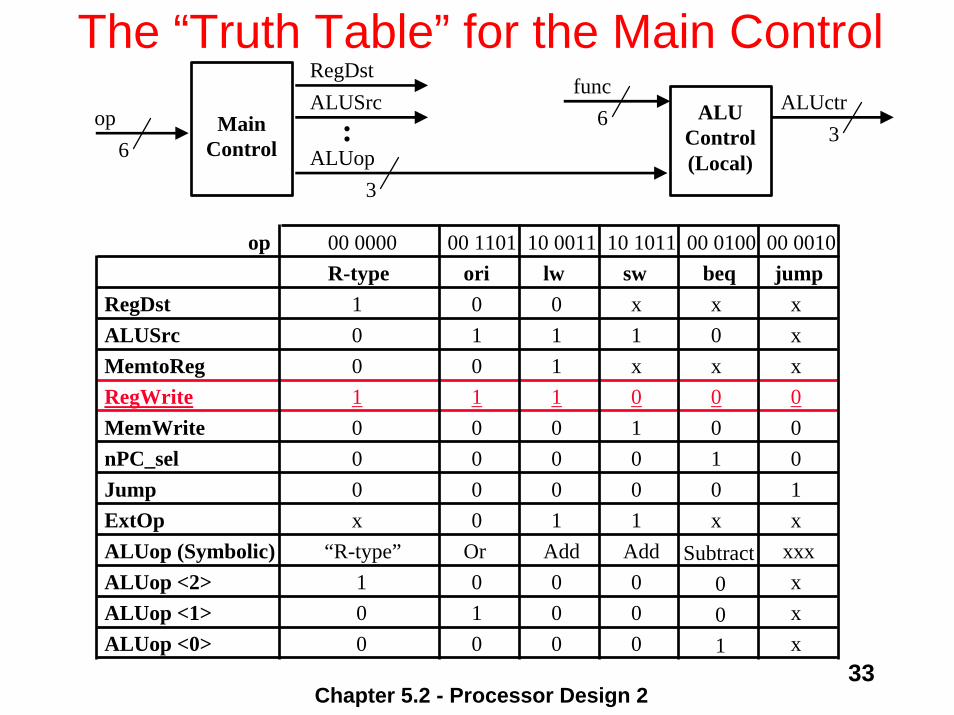
The “Truth Table” for the Main Control
MainControl
op6
ALUControl(Local)
func
3
6
ALUop
ALUctr3
RegDstALUSrc
:
R-type ori lw sw beq jumpRegDstALUSrcMemtoRegRegWriteMemWritenPC_selJumpExtOpALUop (Symbolic)
1001000x
“R-type”
01010000
Or
01110001
Add
x1x01001
Add
x0x0010x
Subtract
xxx0001x
xxx
op 00 0000 00 1101 10 0011 10 1011 00 0100 00 0010
ALUop <2> 1 0 0 0 0 xALUop <1> 0 1 0 0 0 xALUop <0> 0 0 0 0 1 x
Chapter 5.2 - Processor Design 234
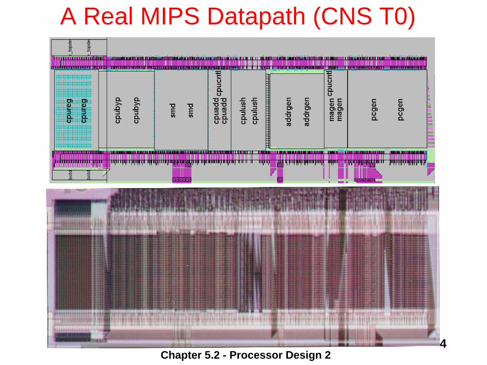
A Real MIPS Datapath (CNS T0)
Chapter 5.2 - Processor Design 235
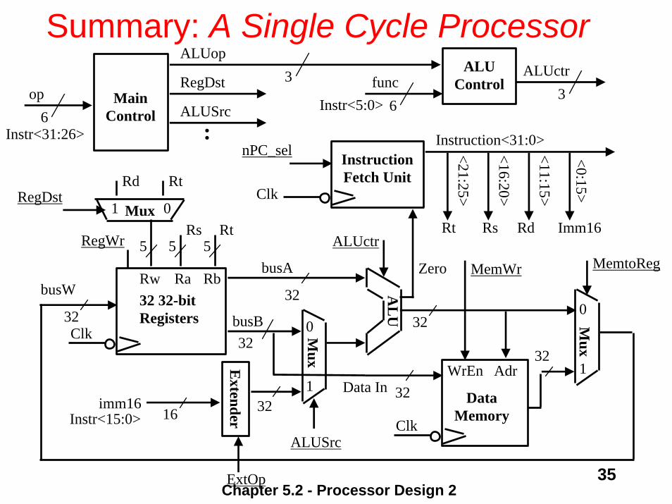
Summary: A Single Cycle Processor
32
ALUctr
Clk
busW
RegWr
3232
busA
32busB
55 5
Rw Ra Rb32 32-bitRegisters
Rs
Rt
Rt
RdRegDst
Extender
Mux
Mux
3216imm16
ALUSrc
ExtOp
Mux
MemtoReg
Clk
Data InWrEn
32Adr
DataMemory
32
MemWrA
LU
InstructionFetch Unit
Clk
Zero
Instruction<31:0>
0
1
0
1
01<21:25>
<16:20>
<11:15>
<0:15>
Imm16RdRsRt
MainControl
op6
ALUControlfunc
6
3ALUop
ALUctr3
RegDst
ALUSrc:
Instr<5:0>
Instr<31:26>
Instr<15:0>
nPC_sel
Chapter 5.2 - Processor Design 236
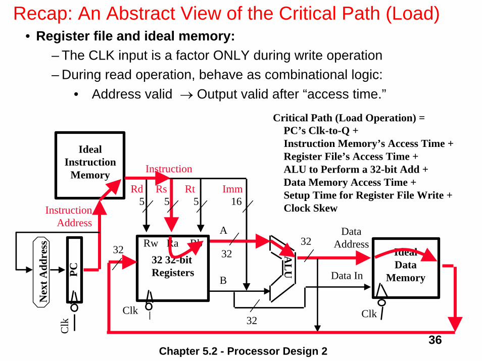
Recap: An Abstract View of the Critical Path (Load)• Register file and ideal memory:
– The CLK input is a factor ONLY during write operation– During read operation, behave as combinational logic:
• Address valid → Output valid after “access time.”
Critical Path (Load Operation) = PC’s Clk-to-Q +Instruction Memory’s Access Time +Register File’s Access Time +ALU to Perform a 32-bit Add +Data Memory Access Time +Setup Time for Register File Write +Clock Skew
Clk
5
Rw Ra Rb32 32-bitRegisters
RdA
LU
Clk
Data In
DataAddress
IdealData
Memory
Instruction
InstructionAddress
IdealInstruction
Memory
Clk
PC
5Rs
5Rt
16Imm
32
323232
A
B
Nex
t Add
ress
Chapter 5.2 - Processor Design 237
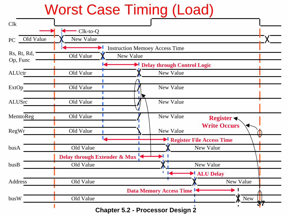
Worst Case Timing (Load)Clk
PC
Rs, Rt, Rd,Op, Func
Clk-to-Q
ALUctr
Instruction Memoey Access Time
Old Value New Value
RegWr Old Value New Value
Delay through Control Logic
busARegister File Access Time
Old Value New Value
busBALU Delay
Old Value New Value
Old Value New Value
New ValueOld Value
ExtOp Old Value New Value
ALUSrc Old Value New Value
MemtoReg Old Value New Value
Address Old Value New Value
busW Old Value New
Delay through Extender & Mux
RegisterWrite Occurs
Data Memory Access Time

Chapter 5.2 - Processor Design 238
Drawback of this Single Cycle Processor
• Long cycle time:– Cycle time must be long enough for the load instruction:
PC’s Clock -to-Q +Instruction Memory Access Time +Register File Access Time +ALU Delay (address calculation) +Data Memory Access Time +Register File Setup Time +Clock Skew• Cycle time for load is much longer than needed for all other
instructions
Chapter 5.2 - Processor Design 239
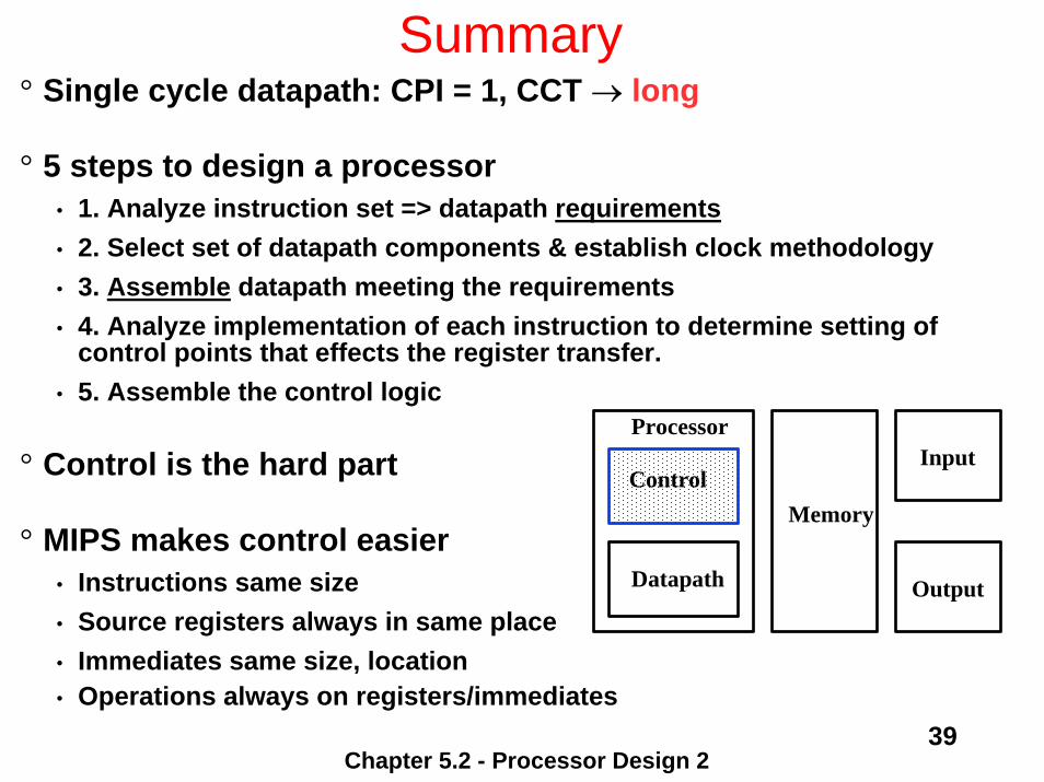
° Single cycle datapath: CPI = 1, CCT → long
° 5 steps to design a processor• 1. Analyze instruction set => datapath requirements• 2. Select set of datapath components & establish clock methodology• 3. Assemble datapath meeting the requirements• 4. Analyze implementation of each instruction to determine setting of
control points that effects the register transfer.• 5. Assemble the control logic
° Control is the hard part
° MIPS makes control easier• Instructions same size• Source registers always in same place• Immediates same size, location• Operations always on registers/immediates
Summary
Control
Datapath
Processor
Memory
Input
Output