process & architecture - flash memory summit · pdf filesanta clara, ca 9 • memory...
TRANSCRIPT

XPoint Memory Comparison
Process & Architecture
Flash Memory Summit 2017
Santa Clara, CA
1
Jeongdong Choe Senior Technical Fellow, TechInsights
Persistent Memory Forum R-12 3D XPoint: Current Implementation s and Future Trends

Contents
Flash Memory Summit 2017
Santa Clara, CA
2
Semiconductor Memory Device Roadmap
XPoint Memory Overview
XPoint Memory Deep Dive
• Process Integration & Materials
• Memory Tile & Cell Design
• Transistors
Leading, Competing or Chasing? • Comparison with DRAM & 3D NAND

Memory Device Roadmap
Flash Memory Summit 2017
Santa Clara, CA
3

Questions About XPoint
Flash Memory Summit 2017
Santa Clara, CA
4
*PCM? Materials?
*Selector? Ternary/Quaternary Phase? As doped?
*Multi-Stacked?
*Layouts? PCM patterning? Double patterning used?
*Memory density? Memory array efficiency?
*Overall memory cell design & architecture?
*Technology Node?
*Die floor plan?
*CMOS under Memory Array?
*Functional blocks? Circuits?
*Top/Middle/Bottom electrodes connection?
*Performance? Transistor parameters? Cell set/reset Current?
*Replace NAND? Replace DRAM?
*# Masks? # Process steps? Process sequence?
*Cost? Cost effective product?
*N+1?, N+2?
*Differences from Micron QuantX?
*Throughput? Yield?
* etc.
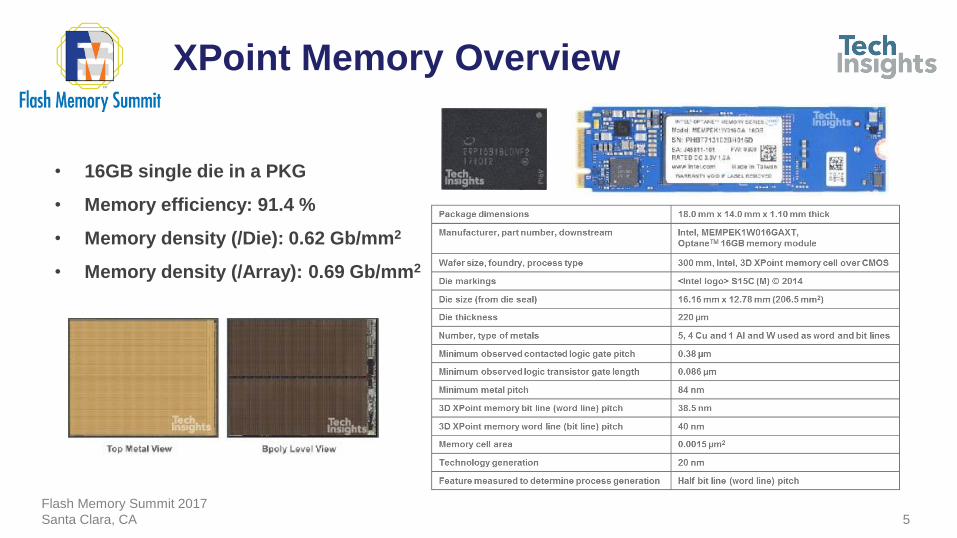
XPoint Memory Overview
Flash Memory Summit 2017
Santa Clara, CA
5
• 16GB single die in a PKG
• Memory efficiency: 91.4 %
• Memory density (/Die): 0.62 Gb/mm2
• Memory density (/Array): 0.69 Gb/mm2
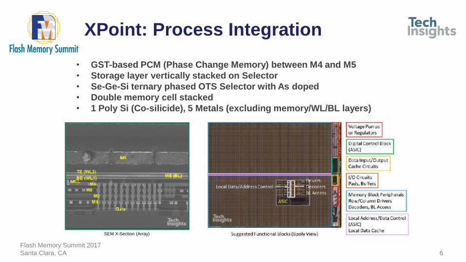
XPoint: Process Integration
Flash Memory Summit 2017
Santa Clara, CA
6
SEM X-Section (Array)
• GST-based PCM (Phase Change Memory) between M4 and M5
• Storage layer vertically stacked on Selector
• Se-Ge-Si ternary phased OTS Selector with As doped
• Double memory cell stacked
• 1 Poly Si (Co-silicide), 5 Metals (excluding memory/WL/BL layers)

XPoint: Memory/OTS Elements
Flash Memory Summit 2017
Santa Clara, CA
7
• Top & bottom cell stacked
• TWL/TE/PCM/ME/OTS/BE/BL2/BL1/TE/PCM/ME/OTS/BE/BWL
• PCM: Ge0.12Sb0.29Te0.54(Si0.05), OTS: Se0.44As0.29Ge0.1Si0.17,
Top Cell
Bottom Cell
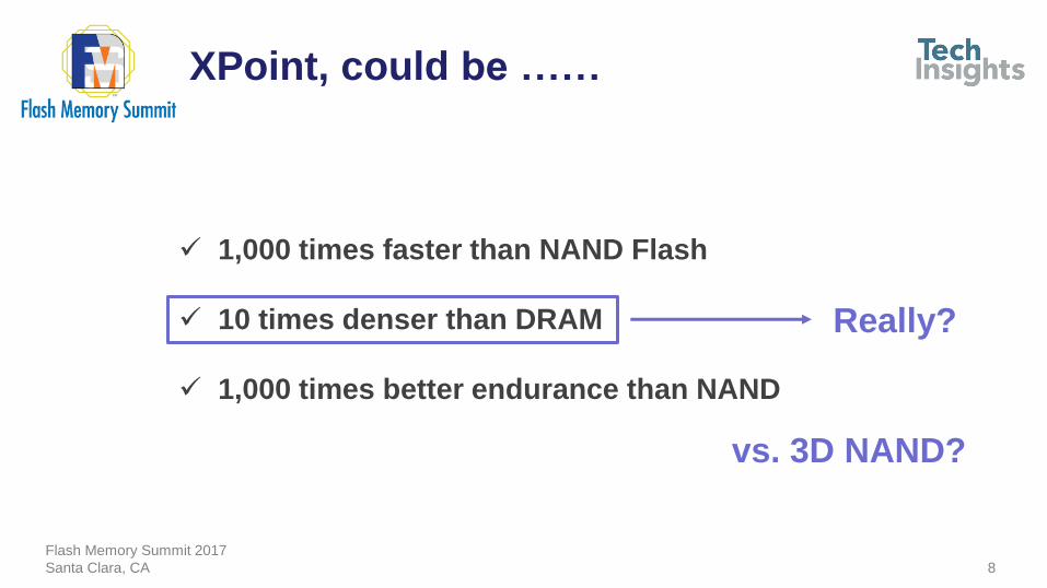
XPoint, could be ……
Flash Memory Summit 2017
Santa Clara, CA
8
1,000 times faster than NAND Flash
10 times denser than DRAM
1,000 times better endurance than NAND
Really?
vs. 3D NAND?
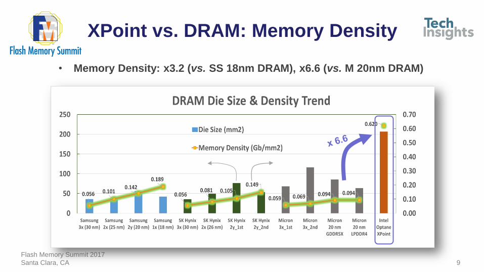
XPoint vs. DRAM: Memory Density
Flash Memory Summit 2017
Santa Clara, CA
9
• Memory Density: x3.2 (vs. SS 18nm DRAM), x6.6 (vs. M 20nm DRAM)

XPoint vs. DRAM: Cell Size
Flash Memory Summit 2017
Santa Clara, CA
10
• Memory Cell Size: 58% (vs. SS 18nm DRAM), 36% (vs. M 20nm DRAM)
(x10-4 µm2)
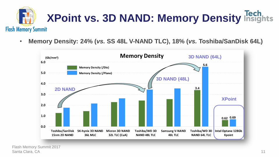
XPoint vs. 3D NAND: Memory Density
Flash Memory Summit 2017
Santa Clara, CA
11
• Memory Density: 24% (vs. SS 48L V-NAND TLC), 18% (vs. Toshiba/SanDisk 64L)
2D NAND
3D NAND (48L)
XPoint
3.4
5.6
3D NAND (64L)
0.62 0.69
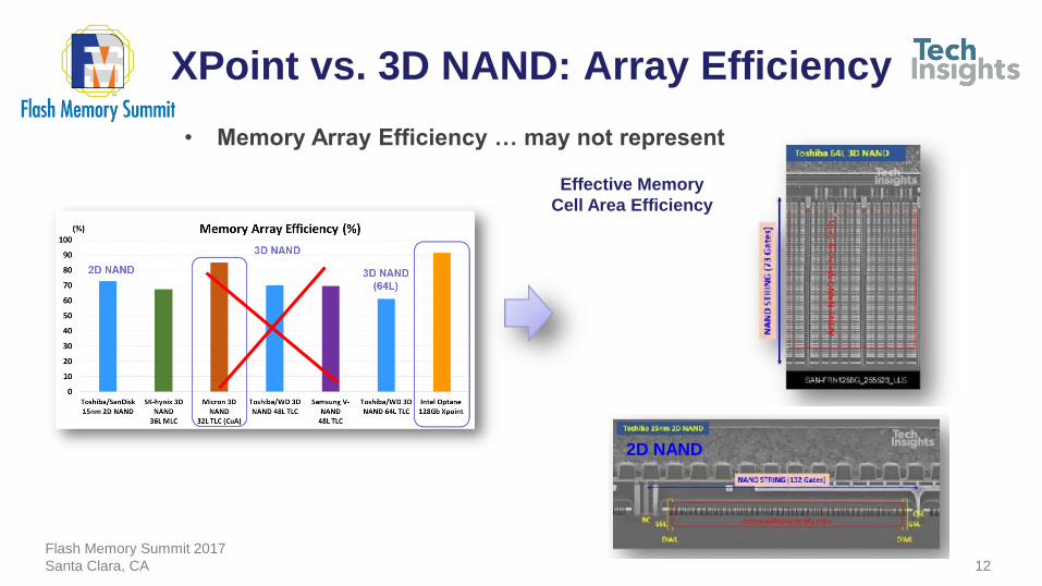
XPoint vs. 3D NAND: Array Efficiency
Flash Memory Summit 2017
Santa Clara, CA
12
• Memory Array Efficiency … may not represent
Effective Memory
Cell Area Efficiency
2D NAND
3D 64L
NAND

XPoint vs. 3D NAND: Array Efficiency
Flash Memory Summit 2017
Santa Clara, CA
13
• Comparison of Effective Memory Cell Area Efficiency: Higher the better
2D NAND
3D NAND 48L
XPoint
64L
43.9%
48L
3D NAND 64L
53.2%

XPoint vs. 3D NAND: Unit Cell Area
Flash Memory Summit 2017
Santa Clara, CA
14
• Comparison of Effective Unit Cell Area: Lower the better
2D NAND
3D NAND
48L 3D NAND
64L
XPoint

XPoint is ……
Flash Memory Summit 2017
Santa Clara, CA
15
6 times denser than Micron 20 nm DRAM
3 times denser than Samsung 1x DRAM
vs. DRAM
vs. NAND
18% memory density of Toshiba/SanDisk 64L NAND
Higher memory cell area efficiency than 2D NAND
Relatively lower cell area efficiency than 3D NAND