proceedings of - technology...
TRANSCRIPT
ICEPMU-2016: Technology Letters Conference Proceedings of the International Conference on Engineering Physics, Materials and Ultrasonics, May 2017
1
PROCEEDINGS OF
International Conference on Engineering Physics,
Materials and Ultrasonics (June 3-4, 2016)
ICEPMU-2016
Editors:
Prof S K Jain, Convener
Dr. Ambika Sharma, HoD
Department of Applied Sciences
The NorthCap University
Gurgaon
Email: [email protected]
Website:www.ncuindia.edu
Sponsored by
Science and Engineering
Research Board
Materials Research
Society of India
Ultrasonic Society of
India
Defence Research and Development
Organization
Organized by
Department of Applied Sciences
Sector 23 A, Gurgaon 122017 - Haryana
Tel: 0124-2365811, Fax: 0124-2367488
Website: www.ncuindia.edu

ICEPMU-2016: Technology Letters Conference Proceedings of the International Conference on Engineering Physics, Materials and Ultrasonics, May 2017
2
Advisory Committee
Prof. Vikram Kumar, I.I.T Delhi & Pres. USI
(Chairman)
Prof. Krishan Lal, NPL, New Delhi
Prof. KL Chopra, NCU Gurgaon
Prof. M.S. Sodha, NCU Gurgaon
Prof. A.K. Ghatak, NCU Gurgaon
Prof. Kehar Singh, NCU Gurgaon
Prof. RC Budhani, I.I.T. Kanpur
Dr. R.K. Sharma, Dir. SSPL, Delhi
Prof. Anurag Kumar, Dir., IISc, Bangalore
Dr. VN Bindal, Patron USI
Prof. ESR Gopal Emer. Sc., IISC Bangalore
Dr. Baldev Raj, Ex-Dir. IGCAR & Pres. Res,
PSG Institutions, Coimbatore
Prof. Yogesh K. Vohra, University of
Alabama at Birmingham, U.S.A.
Dr. Niloy Dutta, Univ. of Connecticut, U.S.A.
Dr. Mekonnen Abebe, Def Univ., Ethiopia.
Dr. Andrej Nowicki, IFTR, Warsaw
Dr. Adam Shaw, NPL (UK), Teddington
Dr. David Gilbert, BINDT, UK
Dr. J. Szilard, Sydney, Australia
Prof. BK Das, NCU Gurgaon
Dr. VR Singh, Advisor, PDM, Bahadurgarh
Prof. Karmeshu, JNU, Delhi
Prof. Promila Goel, NCU Gurgaon
Prof. S.B. Krupanidhi, IISc, Bangalore
Prof. RR Yadav, AU Allahabad
Dr. Chandra Prakash, S.S.P.L. Delhi
Prof. Amitava Sen Gupta, NCU Gurgaon
Prof. P.K. Bhatnagar, South Campus, DU
Prof. S. K. Ray, IIT Kharagpur
Prof. Amlan J. Pal, IACS, Kolkata
Dr. Nitin Goel, Facebook, California
Dr. D. Kanjilal, IUAC, New Delhi
Dr. Avinashi Kapoor, DU, South Campus
Dr. Reji Philip, RR Institute, Bangalore
Chief Patrons
Sh. NK Dewan, Chancellor, NCU
Sh. V Daulet Singh, GB Member, NCU
Sh. Avdhesh Mishra, GB Member, NCU
Sh. Shiv S Mehra, GB Member, NCU
Patrons
Prof. Prem Vrat Pro-chancellor, NCU
Brig. S.K. Sharma, Pro-VC, NCU
Prof. R. Ojha, Director, SOET, NCU
Organizing committees
Convener
Prof. SK Jain, NCU [email protected] Co-conveners
Dr. Rashmi Tyagi
Prof. AK Yadav
Prof.Kallika Srivastava
Dr Devraj Singh, ASET, N. Delhi
Dr.Yudhisther Kumar, NPL, N. Delhi
Technical Program Committee
Dr. Ambika Devi (Chairman) [email protected] Dr. Pranati Purohit
Dr. Sangeet Srivastava
Dr. Kamlesh Sharma
Dr. Amita Bhagat
Dr. Satwanti Devi
Dr. Srijanani
Hospitality Committee
Dr. Hukum Singh (Chairman)
Dr. Ravindra Bisht
Dr. Tejpal Singh
Mr. Manoj Sharma (CSE)
Reception Committee
Dr. Sunanda Vashistha (Chairman)
Dr. Phool Singh
Dr. Sunita Sharma
Dr. Sandeep Mogha
Treasurer Committee
Dr. Pranati Purohit
Dr. Ashutosh Pandey
Dr. Chetna Tyagi
Conference CD and photographs
Dr. Gaurav Gupta (CD proceedings)
Dr. Sangeet Srivastava

ICEPMU-2016: Technology Letters Conference Proceedings of the International Conference on Engineering Physics, Materials and Ultrasonics, May 2017
3
Contents
Sr No Title Author Page No
1 Electrical switching in Cu doped As-Se glasses K. Ramesh, Pumlianmunga,
E.S.R. Gopal
4
2 Bilayer Lift-off Technique for Micromachining Neha Yadav 9
3 Effect of change in titanium isopropoxide
(TTIP) concentration on the preparation of TiO2
nanopowder
Mamta Arya, Shubhra Mathur*,
Rohit Jain
12
4 Calculation Of Some Oscillating Parameters For
Graphene
D. K. Das, K. V. V. Nagaraju, S.
Roy and S. Sahoo
16
5 Study of doped graphene quantum dots by
chlorine containing compounds: Electronic
Spectroscopy
Poonam R. Kharangarh, and
Gurmeet Singh
19
6 Electromagnetic Wave Propagation in Photonic
Structures: Dielectric and Metallo-Dielectric
Waveguides
Triranjita Srivastava, Pushpa
Bindal, Priyanka, Anuradha,
Priyam and Priscilla
23
7 A Comparative Study of Numerical Methods for
Analysing Planar Plasmonic Waveguides
Triranjita Srivastava, Pushpa
Bindal, Asmita Deep and Ashima
Sharda
29
8 Study Of Propagation Characteristics Of Optical
Fibers: Experiment And Simulation
Pushpa Bindal, Triranjita
Srivastava, Sujata, Anju and
Diksha Tandon
33
9 Experimental Study of Microbending Losses in
Optical Fiber
Pushpa Bindal, Triranjita
Srivastava, Ananya, Aastha
Dhankhar
37
10 Growth of (001) oriented Cr and MgO thin
films on Amorphous Substrate for Magnetic
Tunnel Junctions
Sajid Husain, and Sujeet
Chaudhary
41
11 Bio ceramics: Future implant material Aruna Dani 45
12 Intelligent Transportation System Shubham Sehgal, Akshat Mathur,
Mona Aggrawal, Ram Sharma
47
ICEPMU-2016: Technology Letters Conference Proceedings of the International Conference on Engineering Physics, Materials and Ultrasonics, May 2017
4
Electrical switching in
Cu doped As-Se glasses
K. Ramesh*, Pumlianmunga, E.S.R. Gopal
Department of Physics,
Indian Institute of Science, Bangalore 560012,
India.
*Corresponding Author:
Abstract: Bulk CuxAs30Se60-x glasses (0 x 34)
prepared by melt quenching method exhibit
interesting phase change properties when subjected
to high electric fields. The glasses in the
composition range 0 x 14 do not exhibit
switching. Glasses in the composition range 15 x
< 25 exhibit threshold switching. An unusual
switching from low resistance to high resistance
state has been observed for the glasses in the
composition window 25 x 28. A memory
switching is observed for the glasses with x ≥ 30.
The observation of ‘no switching threshold
switching low resistance to high resistance
memory switching’ is unique to Cu-As-Se glasses.
With the thermal crystallization studies and thermal
model, the unique switching behaviour in
CuxAs30Se70-x glasses has been understood.
Key words: Chalcogenide glasses, Electrical
switching, Filament formation, Thermal model,
Thermal crystallization.
1. Introduction
Chalcogenide glasses are known for their electrical
switching and memory effects and are popularly
known as phase change memory materials (PCM)
[1-3]. The application of high current drives the
system from a high resistive (OFF) state to a low
resistive (ON) state. This electrical switching is of
two types namely, threshold and memory [2-3]. The
threshold switching device returns to the high
resistive OFF state once the applied current is
reduced below the holding current (I < Ih). In
contrast, the memory device once switched retains
the ON state even after the applied current is
reduced to zero. The memory device can be brought
back to its high resistive OFF state by the
application of a suitable current pulse. In memory
switching materials, a high conducting crystalline
filament is formed due to the Joule heating at the
time of switching. Threshold switching is reversible
and is generally belie ved to be due to the electronic
transitions. It is also proposed that the presence of
cross-linking elements like Ge, Si, etc., make the
structural reorganization difficult resulting in
threshold switching. Memory switching is
irreversible and requires a structural transition from
glass phase to crystalline phase. So, structural
reorganization is very important for memory
switching to occur [2-3].
The addition of metal atoms significantly alters the
network connectivity, network rigidity, local
structure and consequently the electrical properties
including the switching behaviour [4-7]. The
structural studies show that the metal atoms in
chalcogenide glass network are usually in 4- fold
coordination [8]. As Cu is a monovalent atom, and
for Cu to be in 4- fold coordination, the lone pair
electrons of Se and As atoms are transferred to Cu.
By donating its electrons, the chalcogen atom
increases its local coordination. This transfer of
lone-pair electrons and the changes in the local
structure around each atom influences the optical
and electrical properties to a larger extent [5]. In the
present work, electrical switching in CuxAs30Se70-x
glasses has been studied over a wide composition
range 0 x 35. The observed electrical switching
behaviour of CuxAs30Se70-x glasses has been
understood with the help of thermal crystallization
studies.
2. Experimental
Bulk CuxAs30Se70-x glasses (0 x 35) were
prepared by conventional melt quenching method.
ICEPMU-2016: Technology Letters Conference Proceedings of the International Conference on Engineering Physics, Materials and Ultrasonics, May 2017
5
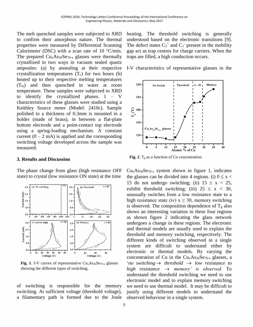
Fig. 1. I-V curves of representative CuxAs30Se70-x glasses
showing the different types of switching.
Fig. 2. Tg as a function of Cu concentration.
The melt quenched samples were subjected to XRD
to confirm their amorphous nature. The thermal
properties were measured by Differential Scanning
Calorimeter (DSC) with a scan rate of 10 °C/min.
The prepared CuxAs30Se70-x glasses were thermally
crystallized in two ways in vacuum sealed quartz
ampoules: (a) by annealing at their respective
crystallization temperatures (Tc) for two hours (b)
heated up to their respective melting temperatures
(Tm) and then quenched in water at room
temperature. These samples were subjected to XRD
to identify the crystallized phases. I – V
characteristics of these glasses were studied using a
Keithley Source meter (Model: 2410c). Sample
polished to a thickness of 0.3mm is mounted in a
holder (made of brass), in between a flat-plate
bottom electrode and a point-contact top electrode
using a spring-loading mechanism. A constant
current (0 – 2 mA) is applied and the corresponding
switching voltage developed across the sample was
measured.
3. Results and Discussion
The phase change from glass (high resistance OFF
state) to crystal (low resistance ON state) at the time
of switching is responsible for the memory
switching. At sufficient voltage (threshold voltage),
a filamentary path is formed due to the Joule
heating. The threshold switching is generally
understood based on the electronic transitions [9].
The defect states C3+ and C1
- present in the mobility
gap act as trap centres for charge carriers. When the
traps are filled, a high conduction occurs.
I-V characteristics of representative glasses in the
CuxAs30Se70-x system shown in figure 1, indicates
the glasses can be divided into 4 regions. (i) 0 x <
15 do not undergo switching; (ii) 15 x < 25,
exhibit threshold switching; (iii) 25 x < 30,
unusually switches from a low resistance state to a
high resistance state (iv) x ≥ 30, memory switching
is observed. The composition dependence of Tg also
shows an interesting variation in these four regions
as shown figure 2 indicating the glass network
undergoes a change in these regions. The electronic
and thermal models are usually used to explain the
threshold and memory switching, respectively. The
different kinds of switching observed in a single
system are difficult to understand either by
electronic or thermal models. By varying the
concentration of Cu in the CuxAs30Se70-x glasses, a
‘no switching threshold low resistance to
high resistance memory’ is observed. To
understand the threshold switching we need to use
electronic model and to explain memory switching
we need to use thermal model. It may be difficult to
justify using different models to understand the
observed behaviour in a single system.
ICEPMU-2016: Technology Letters Conference Proceedings of the International Conference on Engineering Physics, Materials and Ultrasonics, May 2017
6
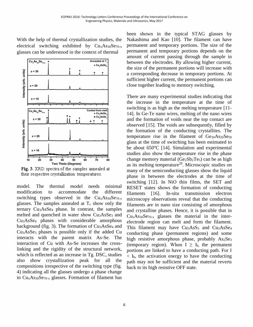
With the help of thermal crystallization studies, the
electrical switching exhibited by CuxAs30Se70-x
glasses can be understood in the context of thermal
model. The thermal model needs minimal
modification to accommodate the different
switching types observed in the CuxAs30Se70-x
glasses. The samples annealed at Tc show only the
ternary Cu3AsSe4 phase. In contrast, the samples
melted and quenched in water show Cu3AsSe3 and
Cu3AsSe4 phases with considerable amorphous
background (fig. 3). The formation of Cu3AsSe4 and
Cu3AsSe3 phases is possible only if the added Cu
interacts with the parent matrix As-Se. The
interaction of Cu with As-Se increases the cross-
linking and the rigidity of the structural network,
which is reflected as an increase in Tg. DSC, studies
also show crystallization peak for all the
compositions irrespective of the switching type (fig.
4) indicating all the glasses undergo a phase change
in CuxAs30Se70-x glasses. Formation of filament has
been shown in the typical STAG glasses by
Nakashima and Kao [10]. The filament can have
permanent and temporary portions. The size of the
permanent and temporary portions depends on the
amount of current passing through the sample in
between the electrodes. By allowing higher current,
the size of the permanent portions will increase with
a corresponding decrease in temporary portions. At
sufficient higher current, the permanent portions can
close together leading to memory switching.
There are many experimental studies indicating that
the increase in the temperature at the time of
switching is as high as the melting temperature [11-
14]. In Ge-Te nano wires, melting of the nano wires
and the formation of voids near the top contact are
observed [15]. The voids are subsequently, filled by
the formation of the conducting crystallites. The
temperature rise in the filament of Ge30As20Se50
glass at the time of switching has been estimated to
be about 650oC [14]. Simulation and experimental
studies also show the temperature rise in the phase
change memory material (Ge2Sb2Te5) can be as high
as its melting temperature29. Microscopic studies on
many of the semiconducting glasses show the liquid
phase in between the electrodes at the time of
switching [12]. In NiO thin films, the SET and
RESET states shows the formation of conducting
filaments [16]. In-situ transmission electron
microscopy observations reveal that the conducting
filaments are in nano size consisting of amorphous
and crystalline phases. Hence, it is possible that in
CuxAs30Se70-x glasses the material in the inter-
electrode region can melt and form the filament.
This filament may have Cu3AsS3 and Cu3AsSe4
conducting phase (permanent regions) and some
high resistive amorphous phase, probably As2Se3
(temporary region). When I ≥ Ih, the permanent
portions are linked to have a conducting path. For I
< Ih, the activation energy to have the conducting
path may not be sufficient and the material reverts
back to its high resistive OFF state.
ICEPMU-2016: Technology Letters Conference Proceedings of the International Conference on Engineering Physics, Materials and Ultrasonics, May 2017
7
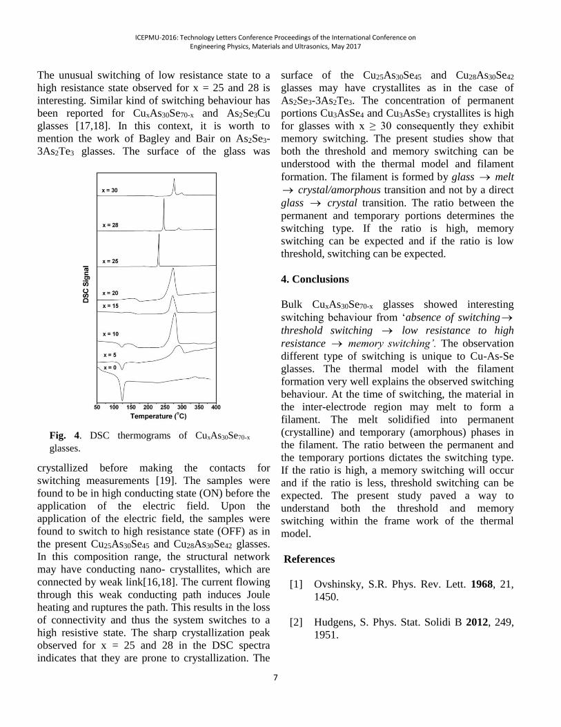
Fig. 4. DSC thermograms of CuxAs30Se70-x
glasses.
The unusual switching of low resistance state to a
high resistance state observed for x = 25 and 28 is
interesting. Similar kind of switching behaviour has
been reported for CuxAs30Se70-x and As2Se3Cu
glasses [17,18]. In this context, it is worth to
mention the work of Bagley and Bair on As2Se3-
3As2Te3 glasses. The surface of the glass was
crystallized before making the contacts for
switching measurements [19]. The samples were
found to be in high conducting state (ON) before the
application of the electric field. Upon the
application of the electric field, the samples were
found to switch to high resistance state (OFF) as in
the present Cu25As30Se45 and Cu28As30Se42 glasses.
In this composition range, the structural network
may have conducting nano- crystallites, which are
connected by weak link[16,18]. The current flowing
through this weak conducting path induces Joule
heating and ruptures the path. This results in the loss
of connectivity and thus the system switches to a
high resistive state. The sharp crystallization peak
observed for x = 25 and 28 in the DSC spectra
indicates that they are prone to crystallization. The
surface of the Cu25As30Se45 and Cu28As30Se42
glasses may have crystallites as in the case of
As2Se3-3As2Te3. The concentration of permanent
portions Cu3AsSe4 and Cu3AsSe3 crystallites is high
for glasses with x ≥ 30 consequently they exhibit
memory switching. The present studies show that
both the threshold and memory switching can be
understood with the thermal model and filament
formation. The filament is formed by glass melt
crystal/amorphous transition and not by a direct
glass crystal transition. The ratio between the
permanent and temporary portions determines the
switching type. If the ratio is high, memory
switching can be expected and if the ratio is low
threshold, switching can be expected.
4. Conclusions
Bulk CuxAs30Se70-x glasses showed interesting
switching behaviour from ‘absence of switching
threshold switching low resistance to high
resistance memory switching’. The observation
different type of switching is unique to Cu-As-Se
glasses. The thermal model with the filament
formation very well explains the observed switching
behaviour. At the time of switching, the material in
the inter-electrode region may melt to form a
filament. The melt solidified into permanent
(crystalline) and temporary (amorphous) phases in
the filament. The ratio between the permanent and
the temporary portions dictates the switching type.
If the ratio is high, a memory switching will occur
and if the ratio is less, threshold switching can be
expected. The present study paved a way to
understand both the threshold and memory
switching within the frame work of the thermal
model.
References
[1] Ovshinsky, S.R. Phys. Rev. Lett. 1968, 21,
1450.
[2] Hudgens, S. Phys. Stat. Solidi B 2012, 249,
1951.
ICEPMU-2016: Technology Letters Conference Proceedings of the International Conference on Engineering Physics, Materials and Ultrasonics, May 2017
8
[3] Bogoslovskiy, N.A.; Tsendin, K.D.
Semiconductors 2012, 46, 559.
[4] Tohge, N.; Minami, T.; Yanamoto, Y.;
Tanaka, M. J. Appl. Phys. 1980, 51,
1048.
[5] Liu, J.Z.; Taylor, P.C. J. Non-Cryst.
Solids 1989, 114, 25
[6] Ramesh, K.; Asokan, S.; Gopal, E.S.R.
J. Non-Cryst. Solids 2006, 352, 2905.
[7] Murugavel, S.; Asokan, S. Phys. Rev. B
1998, 58, 3022.
[8] Xin, S.; Liu, J.; Salmon, P.S. Phys. Rev.
B 2008, 78, 064207.
[9] Adler, D.; Shur, M.S.; Silver, M.;
Ovshinsky, S.R. Appl. Phys. Lett. 1980,
153, 289.
[10] Nakashima, K.; Kao, K.C. J. Non-Cryst.
Solids 1979, 33, 189.
[11] Yang, T.Y.; Park, I.M.; Kim, B.J.; Joo,
Y.C. Appl. Phys. Lett. 2009, 95,
032104.
[12] Pearson, A.D.; Miller, C.E. Phys. Lett.
1969, 14, 280.
[13] Radaelli, A.; Pirovavo, A.; Benvenuti,
A.; Lacaita, L. J. Appl. Phys. 2008, 103,
111101.
[14] Weirauch, D.F. Appl. Phys. Lett. 1970,
16, 72.
[15] Meister, S.; Schoen, T.; Topinka, M.A.;
Minor, A.M.; Cui, Y. Nano Lett. 2008,
8, 4562.
[16] Son, J.Y.; Shin, Y.H. Appl. Phys. Lett.
2008, 92, 222106.
[17] Asahara, Y.; Izumitani, T. J. Non-Cryst.
Solids 1972, 11, 97.
[18] Haifz, M. M.; Ibrahim, M.M.; Dongal,
M. J. Appl. Phys. 1983, 54, 1950.
[19] Bagley, B.G.; Bair, H.E. J. Non-Cryst.
Solids 1970, 2, 155.
Acknowledgements
The authors thank the Department of Science
& Technology (DST) for the financial support.
ICEPMU-2016: Technology Letters Conference Proceedings of the International Conference on Engineering Physics, Materials and Ultrasonics, May 2017
9
Bilayer Lift-off
Technique
for Micromachining
Neha Yadav
Department of Physics,
Keshav Mahavidyalay, University of Delhi
*Corresponding Author:
Abstract:
This paper discusses the application of bilayer
lift off technique for micromachining
applications. In micro-machined devices,
patterning of metal films is required. The metals
can be patterned either by etching or lift-off. In
this paper, using two-layer photoresist for lift-
off has been presented. This technique can be
used for lift-off films having thickness upto 7-8
micron and is very effective in getting desired
photoresist profile.
The prerequisite for the lift-off is negative
profile of the photoresist. The bilayer
photoresist can be patterned using photo mask.
The resultant pattern can be analysed in optical
microscope and SEM. It can be seen that by
varying the flood exposure time of the bottom
layer, negative profile required for lift-off with
desired under-cut could be achieved.
Key words: lift-off, micromachining, negative
profile, under-cut, photoresist
1. Introduction
Micro-machined devices can be fabricated by
either bulk or surface micromachining. Both the
processes require patterning of metals at various
stages of device fabrication. For patterning of
metals, commonly used technique is etching. In
etching the wafer is put in a chemical etchant,
removing the metal from desired places. But in
case of nobel metals or very small dimensions,
lift-off is preferred.
Following are the general steps involved in the
lift-off process:
A thin layer of photoresist is spin coated on the
substrate, dried off and exposed to UV radiation
through a pattern and developed using a
developer. After the development process,
patterned photoresist is obtained. The wafer is
then placed in vacuum chamber and thermal
deposition of metallic thin film is done by
‘thermal evaporation’. The slide is placed in a
solvent which seeps under and dissolves the
photoresist and the film which is directly
deposited is left behind on the substrate.
Following are the requirements for a metallic
film to be lifted-off:
1. Temperature should not be very high
otherwise the photoresist might get
burnt.
2. The metal thickness is to be around or
less 100nm to allow solvent seep under
it and dissolve the photoresist.
3. The deposition of film on the substrate is
to be very good.
4. The film is to be easily wetted by the
solvent.
5. The film is not to be elastic but brittle,
otherwise it will tear along adhesion
lines.
6. The film quality is not absolutely
critical. That means if requirements on
film quality are stringent, then, lift-off is
not to be used Photoresist will outgas
very slightly in vacuum systems, which
may adversely affect the quality of the
deposited film.
2. Important parameters for desired Lift-
off
Result:
1. It is important to create negative slope
profile or undercut profile so that lift-
off becomes easy.
2. Prebake temperature has the greatest
influence on negative slope rate. The
parameters which have influence are
ICEPMU-2016: Technology Letters Conference Proceedings of the International Conference on Engineering Physics, Materials and Ultrasonics, May 2017
10
prebake time, UV exposure intensity
and time of photoresist, the developer,
the mode of development and time of
development.
3. Careful consideration should be given
to the resist/developer system
3. Different methods for lift-off
technique
Depending on requirements different
methods are employed.
1. Single Layer Resist Processing
a) Standard Photoresist Processing: Only
one mask step and the standard
photolithography procedure are
involved. The main disadvantage of this
method is that the film is deposited on
the sidewall of the photoresist, and
adheres to the substrate even after the
resist removal. This sidewall may be
peeled off in subsequent processing,
resulting in particulates and shorts, or it
may flop over and interfere with etches
or depositions that follow.
b) Single Layer lift off technique using
negative photoresist.
c) Very Thick Negative Photoresist Single
Layer
2. Bi-Layer Resist Processing
a) PR/LOL 2000
b) PR/ LOR Lift-Off Resist (or PMGI
Resist)
c) PMMA/PMMA
d) PMMA/LOL2000
e) Composite Layers of Aluminum (Al)
and Photoresist
3. Tri-Layer Processing
4. Surface Modified Resist Processing
The need for using lift-off technique instead of
etching by conventional methods is that for noble
elements such as Gold, Nickel, Platinum,
Tantalum, Titanium and others, the etching
chemicals may not be available. The substrate or
layers may be sensitive to harsh chemicals. The
harsh chemicals may degrade the quality of the
substrate (semiconductor) and thereby affecting
its quality of performance. Also, smaller the
dimensions etch control becomes more difficult.
Lift-off technique using Positive photoresists
Positive photoresists are preferred in the IC
industry or MEMS foundries due to their ease of
removal and better resolution capabilities But
for the lift-off applications , the positive
photoresists have the limitation of lower
softening points (around 120-130°C). This
range of temperatures is reached even during the
normal coating and hence the resist features
rounding and makes it very difficult even
impossible to lift-off. Another drawback is that,
by using positive photoresists only positive
profile or at the most vertical profile is obtained
covering the sidewalls during coating and hence
making lift-off difficult. If the desired pattern is
such that positive photoresists is to be used then
the positive resist used should have higher
thermal stability and sidewalls of the photoresist
should be very steep.
4. Experimental Procedure
In bilayer lift-off technique, as the name
suggests two layers of photoresist is used with
different flood exposure time.
A thin film of the assisting material is deposited
over the substrate and it is exposed to UV light
without masking. A layer of photoresist is spin
coated on the substrate and again exposed to
UV radiation through a pattern. The mask
exposure time is less than the previous exposure
time without masking and developed using
developer. The underlying layer of the assisted
material is etched by the developer. Metallic
thin film is deposited by ‘evaporation’ process.
The photoresist is removed and the layer of
metal also gets removed along with it and
finally the underlying layer of assisted material
is also removed and well defined metal pattern
alone is left.
ICEPMU-2016: Technology Letters Conference Proceedings of the International Conference on Engineering Physics, Materials and Ultrasonics, May 2017
11
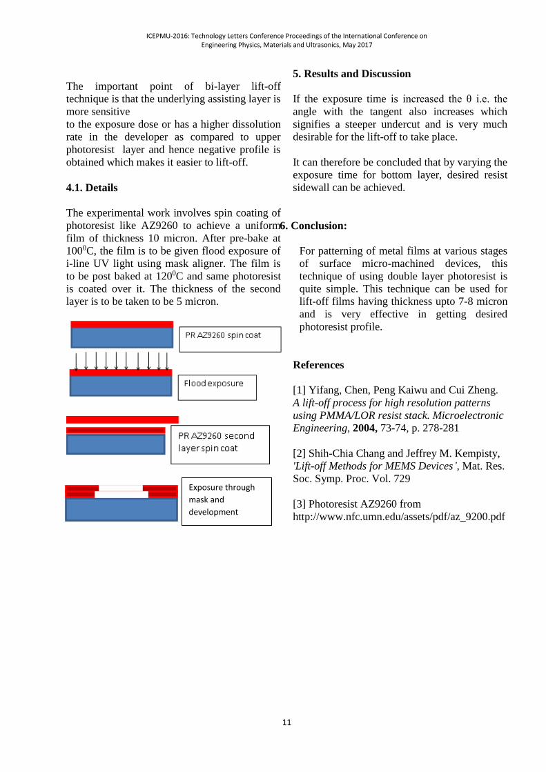
The important point of bi-layer lift-off
technique is that the underlying assisting layer is
more sensitive
to the exposure dose or has a higher dissolution
rate in the developer as compared to upper
photoresist layer and hence negative profile is
obtained which makes it easier to lift-off.
4.1. Details
The experimental work involves spin coating of
photoresist like AZ9260 to achieve a uniform
film of thickness 10 micron. After pre-bake at
1000C, the film is to be given flood exposure of
i-line UV light using mask aligner. The film is
to be post baked at 1200C and same photoresist
is coated over it. The thickness of the second
layer is to be taken to be 5 micron.
5. Results and Discussion
If the exposure time is increased the θ i.e. the
angle with the tangent also increases which
signifies a steeper undercut and is very much
desirable for the lift-off to take place.
It can therefore be concluded that by varying the
exposure time for bottom layer, desired resist
sidewall can be achieved.
6. Conclusion:
For patterning of metal films at various stages
of surface micro-machined devices, this
technique of using double layer photoresist is
quite simple. This technique can be used for
lift-off films having thickness upto 7-8 micron
and is very effective in getting desired
photoresist profile.
References
[1] Yifang, Chen, Peng Kaiwu and Cui Zheng.
A lift-off process for high resolution patterns
using PMMA/LOR resist stack. Microelectronic
Engineering, 2004, 73-74, p. 278-281
[2] Shih-Chia Chang and Jeffrey M. Kempisty,
'Lift-off Methods for MEMS Devices’, Mat. Res.
Soc. Symp. Proc. Vol. 729
[3] Photoresist AZ9260 from
http://www.nfc.umn.edu/assets/pdf/az_9200.pdf
Exposure through
mask and
development
ICEPMU-2016: Technology Letters Conference Proceedings of the International Conference on Engineering Physics, Materials and Ultrasonics, May 2017
12
Effect of change in
titanium isopropoxide
(TTIP) concentration
on the preparation of
TiO2 nanopowder
Mamta Arya, Shubhra Mathur*, Rohit Jain
Department of Physics, JaganNath Gupta Institute
of Engineering & Technology, Jaipur, 303905,
India
*Corresponding author.
E-mail: [email protected],
Abstract TiO2 nano-powder is prepared by
changing titanium isopropoxide (TTIP)
concentration as 3.5 ml, 4.5 ml and 5.5 ml in 40 ml
methanol and thus annealing at 6000 C. X-ray
diffraction (XRD) pattern exhibits the presence of
mixed phase anatase/rutile in various TiO2
nanopowder specimens prepared by different
concentrations of TTIP. It was observed that the
content of rutile phase is more in case of 5.5 ml
TITP as compared to 4.5 ml and 3.5 ml TTIP of
TiO2 nanopowder specimens. The average
crystallite size was found to be 35±5 nm for TiO2
nanopowder specimens. UV studies show that
indirect and direct band gap lies in the range of
2.95-2.76 eV for different TTIP concentrations 3.5
ml, 4.5 ml and 5.5 ml of TiO2 nanopowder
specimens.
Keywords: nanopowder, band gap, XRD, TiO2
1. Introduction
Titanium dioxide (TiO2) is considered as the most
promising semiconductor metal oxide because it
exhibits highly enhanced photo catalytic activity
[1] and improvement in gas sensing properties [2].
Anatase, rutile and brookite are three well known
phases of TiO2 amongst which rutile is a high
temperature stable phase. However, anatase and
brookite are metastable phases and transform to
rutile on heating. Anatase phase show an energy
band gap of 3.2 eV whereas rutile phase exhibits an
optical band gap of 3.0 eV [3].
Sol-gel is a versatile method used for the
preparation of TiO2 nanopowder [4-5]. The change
in concentration of titanium isopropoxide, which
acts as a starting material in our investigation, may
lead to change in structural and optical properties
of TiO2. This motivated us to carry out the present
study.
2. Experimental
2.1. Materials
Titanium isopropoxide (TTIP) and methanol are
used as starting materials. The chemicals used are
of analytical research (AR) grade.
2.2. Methods
TiO2 nanopowder is prepared by using sol gel
method. Sol-gel process also known as a wet-
chemical technique is used for the fabrication of
both glassy and ceramic materials. In this process,
the sol (or solution) evolves gradually towards the
formation of a gel-like network containing both a
liquid phase and a solid phase [5].
2.2.1. Preparation of Samples
Titanium isopropoxide (TTIP) taken in different
concentrations as 3.5 ml, 4.5 ml and 5.5 ml is
mixed in 40 ml methanol. This results in a milky
white solution and is vigorously stirred for 1:30
hours at a temperature 57±3⁰C. The gel thus
produced is kept for drying at room temperature for
12 hrs. Hence the powder is obtained and annealed
at 600⁰C for 1 hour in air [5].
3. Results & Discussion
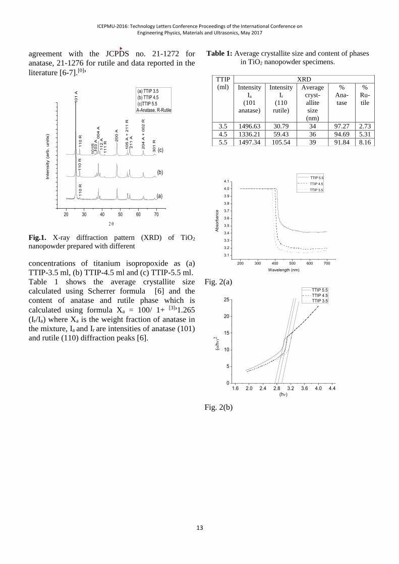
X-Ray diffraction pattern (XRD) of TiO2
specimens having different concentration of (TTIP)
is recorded using Cu-Kα radiation as shown in
Fig1. Diffraction peaks showing the presence of
both anatase and rutile phase are in good
ICEPMU-2016: Technology Letters Conference Proceedings of the International Conference on Engineering Physics, Materials and Ultrasonics, May 2017
13
agreement with the JCPDS no. 21-1272 for
anatase, 21-1276 for rutile and data reported in the
literature [6-7].[0]› 101 A
20 30 40 50 60 70
111 R
110 R
110 R
301 R
204 A
+ 0
02 R
211 A
105 A
+ 2
11 R
200 A
112 A
004 A
101R
103 A
110 R
Inte
nsity (
arb
. u
nits)
(a) TTIP 3.5
(b) TTIP 4.5
(c)TTIP 5.5
A-Anatase, R-Rutile
(a)
(b)
(c)
Fig.1. X-ray diffraction pattern (XRD) of TiO2
nanopowder prepared with different
concentrations of titanium isopropoxide as (a)
TTIP-3.5 ml, (b) TTIP-4.5 ml and (c) TTIP-5.5 ml.
Table 1 shows the average crystallite size
calculated using Scherrer formula [6] and the
content of anatase and rutile phase which is
calculated using formula Xa = 100/ 1+ [3]›1.265
(Ir/Ia) where Xa is the weight fraction of anatase in
the mixture, Ia and Ir are intensities of anatase (101)
and rutile (110) diffraction peaks [6].
Table 1: Average crystallite size and content of phases
in TiO2 nanopowder specimens.
200 300 400 500 600 700
3.1
3.2
3.3
3.4
3.5
3.6
3.7
3.8
3.9
4.0
4.1
Ab
so
rba
nce
Wavelength (nm)
TTIP 5.5
TTIP 4.5
TTIP 3.5
Fig. 2(a)
1.6 2.0 2.4 2.8 3.2 3.6 4.0 4.40
5
10
15
20
25
(h
(h)
TTIP 5.5
TTIP 4.5
TTIP 3.5
Fig. 2(b)
TTIP
(ml)
XRD
Intensity
Ia
(101
anatase)
Intensity
Ir
(110
rutile)
Average
cryst-
allite
size
(nm)
%
Ana-
tase
%
Ru-
tile
3.5 1496.63 30.79 34 97.27 2.73
4.5 1336.21 59.43 36 94.69 5.31
5.5 1497.34 105.54 39 91.84 8.16
ICEPMU-2016: Technology Letters Conference Proceedings of the International Conference on Engineering Physics, Materials and Ultrasonics, May 2017
14
1.6 2.0 2.4 2.8 3.2 3.6 4.0 4.41.4
1.5
1.6
1.7
1.8
1.9
2.0
2.1
2.2
(h
(h
TTIP 5.5
TTIP 4.5
TTIP 3.5
Fig. 2(c)
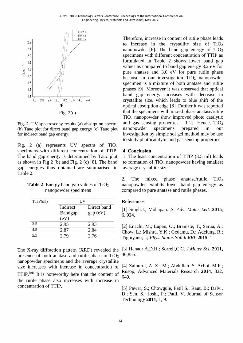
Fig. 2. UV spectroscopy results (a) absorption spectra
(b) Tauc plot for direct band gap energy (c) Tauc plot
for indirect band gap energy.
Fig. 2 (a) represents UV spectra of TiO2
specimens with different concentration of TTIP.
The band gap energy is determined by Tauc plot
as shown in Fig 2 (b) and Fig. 2 (c) [8]. The band
gap energies thus obtained are summarised in
Table 2.
Therefore, increase in content of rutile phase leads
to increase in the crystallite size of TiO2
nanopowder [6]. The band gap energy of TiO2
specimens with different concentration of TTIP as
formulated in Table 2 shows lower band gap
values as compared to band gap energy 3.2 eV for
pure anatase and 3.0 eV for pure rutile phase
because in our investigation TiO2 nanopowder
specimen is a mixture of both anatase and rutile
phases [9]. Moreover it was observed that optical
band gap energy increases with decrease in
crystallite size, which leads to blue shift of the
optical absorption edge [8]. Further it was reported
that the specimens with mixed phase anatase/rutile
TiO2 nanopowder show improved photo catalytic
and gas sensing properties [1-2]. Hence, TiO2
nanopowder specimens prepared in our
investigation by simple sol gel method may be use
to study photocatalytic and gas sensing properties.
4. Conclusion
1. The least concentration of TTIP (3.5 ml) leads
to formation of TiO2 nanopowder having smallest
average crystallite size.
Table 2: Energy band gap values of TiO2
nanopowder specimens
The X-ray diffraction pattern (XRD) revealed the
presence of both anatase and rutile phase in TiO2
nanopowder specimens and the average crystallite
size increases with increase in concentration of
TTIP.[0]› It is noteworthy here that the content of
the rutile phase also increases with increase in
concentration of TTIP.
2. The mixed phase anatase/rutile TiO2
nanopowder exhibits lower band gap energy as
compared to pure anatase and rutile phases.
References
[1] Singh.J.; Mohapatra,S. Adv. Mater Lett. 2015,
6, 924.
[2] Enachi, M.; Lupan, O.; Braniste, T.; Sarua, A.;
Chow, L.; Mishra, Y.K.; Gedamu, D.; Adelung, R.;
Tiginyanu, I.; Phys. Status Solidi RRL 2015, 1
[3] Hanaor,A.D.H.; Sorrell,C.C. J Mater Sci. 2011,
46,855.
[4] Zainurul, A. Z.; M.; Abdullah. S. Achoi, M.F.;
Rusop, Advanced Materials Research 2014, 832,
649.
[5] Pawar, S.; Chowgule, Patil S.; Raut, B.; Dalvi,
D.; Sen, S.; Joshi, P.; Patil, V. Journal of Sensor
Technology 2011, 1, 9.
TTIP(ml) UV
Indirect
Bandgap
(eV)
Direct band
gap (eV)
3.5 2.95 2.93 4.5 2.87 2.84 5.5 2.79 2.76

ICEPMU-2016: Technology Letters Conference Proceedings of the International Conference on Engineering Physics, Materials and Ultrasonics, May 2017
15
[6] Dai, S.; Wu, Y.; Sakai, T.; Du, Z.; Sakai, H.;
Abe, M. Nanoscale Research Letters, 2010, 5,
1829.
[7] Vijayalakshmi, K.; Rajendran, K.V. 2010,
AZojomo 2010, 6, DOI: 10.2240/azojomo0298
[8] Tripathi, A.K.; Singh, M. K.; Mathpal, M. C. ;
Mishra, S. K. ; Agarwal, A. Journal of Alloys and
Compounds, 2013, 549, 114.
[9] Paul, S.; Choudhury, A. Appl Nano Sci 2014,
4, 839.
Acknowledgment
Authors thank Science & Engineering Research
Board (SERB) for providing financial grant vide
no SERB/F/5303/2014-15 and MRC, MNIT, Jaipur
for XRD facility.
ICEPMU-2016: Technology Letters Conference Proceedings of the International Conference on Engineering Physics, Materials and Ultrasonics, May 2017
16
Calculation of Some
Oscillating Parameters
For Graphene D. K. Das*1, K. V. V. Nagaraju2, S. Roy 3 and S.
Sahoo4
1Department of Metallurgical and Materials Engineering
National Institute of Technology, Durgapur-713209, West
Bengal, India. 2, 3, 4Department of Physics, National Institute of Technology
Durgapur-713209, West Bengal, India.
*Corresponding Author: [email protected]
Abstract In recent years graphene has become a
hot topic of research in various sectors due to its
many advanced properties such as high tensile
strength, stiffness etc. It is a two-dimensional (2D)
nanomaterial. Reduced dimensional structure makes
graphene mechanically rigid and stiffest ever. Frank
et al. have experimentally studied effective spring
constant of stacks of suspended graphene sheets
(less than 5) and found the value of spring constant
lies in the range 1 to 5 N/m. In this paper, we
calculate the frequency, spring constant and
damping coefficient of graphene under oscillation
due to tensile force theoretically.
Keywords: Graphene; frequency; spring constant; damping
coefficient.
1. Introduction
Graphene is sp2 hybridized, single atomic layer
hexagonally arranged network of carbon atoms. A
single pi (π) bond and three sigma (σ) bonds joins
each carbon atom in graphene with its neighboring
carbon atoms. A loan pair of free motile electrons
forms each pi bond. The soft, lustrous and
lubricating nature of graphene is due to presence of
these free electrons. They also results in high
electrical and thermal conductivity of graphene [1,
2]. Graphene has an electron mobility of 2.5 × 10⁵
cm2 V-1 s-1 [1].
Frank et al. [3] have experimentally studied
effective spring constant of stacks of suspended
graphene sheets (less than 5) and found the value of
spring constant lies in the range 1 to 5 N/m. In this
paper, we intend to determine some oscillating
parameters such as frequency, spring constant and
damping coefficient of a graphene sheet under
oscillation due to tensile force theoretically.
This paper is organized as follows: In Sec. 2, we
calculate the frequency (ωnA), spring constant (K)
and damping coefficient (Cc) of a graphene sheet
under oscillation due to tensile force. In Sec. 3, we
discuss our results. In Sec. 4, we present our
conclusion.
Calculation of oscillating parameters for
graphene
Let us consider a graphene sheet with dimension
800×300 nm in length and breadth respectively
which is being fixed at one end. A force is applied
at the other end and released. The sheet starts
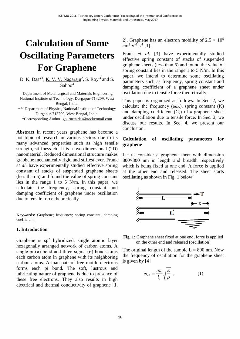
oscillating as shown in Fig. 1 below:
Fig. 1: Graphene sheet fixed at one end, force is applied
on the other end and released (oscillation)
The original length of the sample L = 800 nm. Now
the frequency of oscillation for the graphene sheet
is given by [4]
E
l
n
e
nA , (1)
ICEPMU-2016: Technology Letters Conference Proceedings of the International Conference on Engineering Physics, Materials and Ultrasonics, May 2017
17
where n = mode value =1 (for here), el = effective
length of sheet = 750 nm (say), = density of
graphene = 2300 kg/m3 and E = Young’s modulus
of graphene sheet = 1 TPa [5]. Putting these values
in equation (1), we get ωnA = 8.7298×10¹⁰ rad/s or
1.39×10¹⁰ Hz. Again we know time period of
oscillation for a vibrating body is given by [6]
, (2)
where, ω is the frequency for oscillation (ωnA) for
this case. The time period of oscillation for the said
graphene sheet is found to be 7.1937×10⁻¹¹ s. The
relation between frequency and spring constant for
oscillation motion is given by the relation [6]
m
Kf n
2
1 , (3)
where, m is the mass of the object and K is the
spring constant.
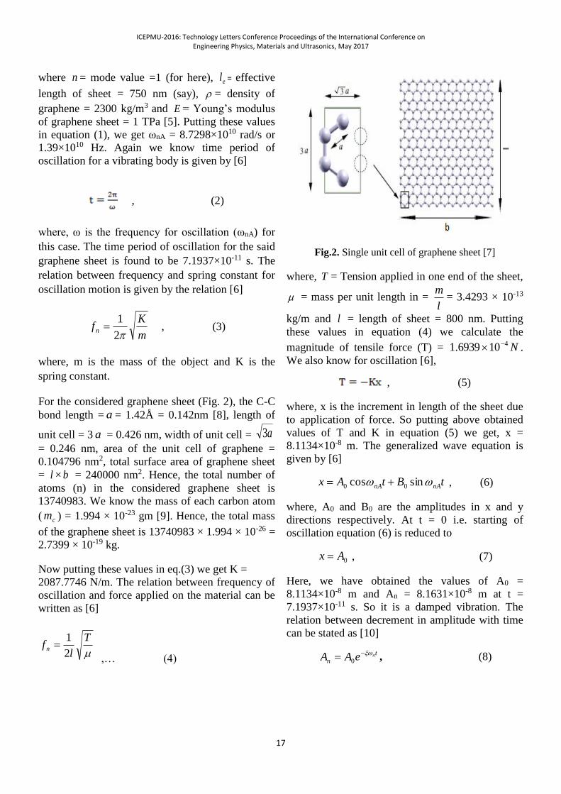
For the considered graphene sheet (Fig. 2), the C-C
bond length = a = 1.42Å = 0.142nm [8], length of
unit cell = 3 a = 0.426 nm, width of unit cell = a3
= 0.246 nm, area of the unit cell of graphene =
0.104796 nm2, total surface area of graphene sheet
= l × b = 240000 nm2. Hence, the total number of
atoms (n) in the considered graphene sheet is
13740983. We know the mass of each carbon atom
( cm ) = 1.994 × 10⁻²³ gm [9]. Hence, the total mass
of the graphene sheet is 13740983 × 1.994 × 10-26 =
2.7399 × 10⁻¹⁹ kg.
Now putting these values in eq.(3) we get K =
2087.7746 N/m. The relation between frequency of
oscillation and force applied on the material can be
written as [6]
T
lf n
2
1
,… (4)
Fig.2. Single unit cell of graphene sheet [7]
where, T = Tension applied in one end of the sheet,
= mass per unit length in = l
m= 3.4293 × 10⁻¹³
kg/m and l = length of sheet = 800 nm. Putting
these values in equation (4) we calculate the
magnitude of tensile force (T) = N4106939.1 .
We also know for oscillation [6],
, (5)
where, x is the increment in length of the sheet due
to application of force. So putting above obtained
values of T and K in equation (5) we get, x =
8.1134×10⁻⁸ m. The generalized wave equation is
given by [6]
tBtAx nAnA sincos 00 , (6)
where, A0 and B0 are the amplitudes in x and y
directions respectively. At t = 0 i.e. starting of
oscillation equation (6) is reduced to
0Ax , (7)
Here, we have obtained the values of A0 =
8.1134×10⁻⁸ m and An = 8.1631×10⁻⁸ m at t =
7.1937×10⁻¹¹ s. So it is a damped vibration. The
relation between decrement in amplitude with time
can be stated as [10]
t
nneAA
0 , (8)
ICEPMU-2016: Technology Letters Conference Proceedings of the International Conference on Engineering Physics, Materials and Ultrasonics, May 2017
18
where, ξ is the damping ratio. Putting the above
values in equation (8) we get ξ = -9.7245×10⁻⁶. The
coefficient of critical damping (Cc) is given by [10]
, (9)
Using the values of K and m in equation (9), we get
Cc = 4.7834×10⁻⁸ kg/s. Further, we know that [10]
ξ = C/ CC , (10)
where, C is the coefficient of damping. From here
we calculate C = 4.5616×10⁻¹³ kg/s.
2. Results
We have found that the oscillation parameters for
graphene are depending on the Young’s modulus
and size of the material. Complete analytical work
is carried out with a graphene sheet of dimensions
(800nm×300nm). Our results show that mechanical
stiffness of our graphene sheet (K= 20784.1996
N/m) is much higher than previously reported
values. Our calculated parameters are reported in
tabular form below:
Table:1. Oscillating parameters for graphene
Sl.
No.
Oscillating Parameters Our calculated values
1. Frequency of vibration
(ωnA)
8.7298×10¹⁰ rad/s
2. Spring constant (K) 2087.7746 N/m
3. Damping Coefficient 4.5616×10⁻¹³ kg/s.
3. Conclusion
Analysis on these oscillating parameters of
graphene is very useful to study its mechanical
properties. These are also useful to design the
nanomechanical resonators and
nanoelectromechanical resonator sensors because
graphene shows ultra-high sensitivity of vibrations.
We hope our results can be useful for the design of
the next generation nanodevices and
nanofabrication technologies that use the vibration
properties of graphene. Our theoretical results
would be verified theoretically as well as
experimentally in future for confirmation.
Acknowledgement
Mr. K. V. V. Nagaraju thanks NIT Durgapur for
providing fellowship during his M. Tech. study.
References
[1] Novoselov, K. S; Fal′ko, V. I; Colombo, L;
Gellert, P. R; Schwab, M. G; Kim, K; Nature,
2012, 490, 192.
[2] Maity, S; Ganguly, M.; Elements of Chemistry-
1, Publishing Syndicate; Kolkata, 2003.
[3] Frank, I. W; Tanenbaum, D. M: J Vac. Sci.
Technol. B, 2007, 25(6), 2558.
[4] Gupta, S. S; Batra, R. C; J. Comput. Theor.
Nanosci., 2010, 7, 1.
[5] Lee, C; Wei, X; Kysar, J. W; Hone, J; Science,
2008, 321(5887), 385.
[6] Datta, D; Pal, B; Chaudhuri, B; Elements of
Higher Secondary Physics-1, Publishing
Syndicate, Kolkata, 2002.
[7] Yamayose, Y; Kinoshita, Y; Doi, Y; Nakatani,
A; Kitamura, T; Eur. Phys. Lett., 2007, 80, 40008.
[8] Fujita, T. K. W; Oshima, C; Surface and
Interface Analysis., 2005, 37(2), 120.
[9]http://chemistry.about.com/od/workedchemistry
problems/a/avogadroexampl1.htm.
[10] Nag, D; Mechanical Vibrations, Wiley, Delhi,
2011.
ICEPMU-2016: Technology Letters Conference Proceedings of the International Conference on Engineering Physics, Materials and Ultrasonics, May 2017
19
Study of doped
graphene quantum dots
by chlorine containing
compounds: Electronic
Spectroscopy Poonam R. Kharangarh*, and Gurmeet Singh
Department of Chemistry, University of Delhi,
Delhi 110007, India
*Corresponding Author:
Abstract: For the study of high quality doped
graphene quantum dots, a series of chlorine
containing compounds such as CoCl2, HCl, and
NH4Cl were used. The morphology of the samples
were done by Transmission Electron Microscope
(TEM). The absorption of the doped material was
found by U-V visible spectroscopy for optical
study. The redox behaviour has been observed by
using Cyclic Voltammetry tool. Different electronic
structures for different doped graphene quantum
dots were observed from UV- Visible
Spectroscopy. Cyclic Voltammetry measurements
show the oxidation and reduction of different metal
doped GQDs to calculate the energy for the
conduction band edges parameters (HOMO and
LUMO).
Key words: Graphene Quantum Dots, TEM, UV-
Visible, Transition Metals, Energy Gap, HOMO,
LUMO
1. Introduction
Graphene Quantum Dots (GQDs), fragments of
graphene has been brought tremendous attention
due to their physical properties, including excellent
water solubility, low cytotoxicity, excellent
biocompatibility, and resistance to photo-bleaching
[1-4].
Doping with different metals is the most realistic
tool to tune the semiconducting properties in the
conventional semiconductor community.
Nevertheless, due to presence of low defects in un-
doped GQDs, weak optical properties can be seen.
Doping heteroatoms including boron, nitrogen,
chlorine, sulphur, fluorine can improve the
electronic characteristics of GQDs to introduce
more defects [5-8]. Nevertheless, bandgap is
increased in GQDs after doping with different
heteroatoms showing ideal p- and n-type
semiconducting electronic properties for potential
applications of GQDs in electronic devices.
A lot of research has been declared that the doping
of different atoms into GQDs alters the band gap
between conduction band maximum and valence
band minimum. Results were shown that a new
energy level was introduced to tune the optical
properties in order to make GQDs for solar cells
applications. In order to fulfill the energy
requirements and to generate the photo-current, we
need to choose a appropriate material which can
modify the energy band structure. Herein, we
present a facile hydrothermal method to prepare
doped GQDs with different transition metals having
chlorine containing elements. When chlorine
containing compounds are doped into GQDs, it
usually has different absorption bands induced by
edge effect in modified GQDs. Furthermore, the
effect of metals on the electronic structure of GQDs
still remains unclear. Hence, there is a need to
investigate how these metals modifies the energy-
level structure in case of doped-GQDs. Cyclic
voltammetry characterization technique [9-11]
reveals that the different band gap is obtained upon
the integration of chlorates into the GQDs.
2. Experimental
2.1. Materials
ICEPMU-2016: Technology Letters Conference Proceedings of the International Conference on Engineering Physics, Materials and Ultrasonics, May 2017
20
In this work we have used commercially available
graphite powder, NaNO3, KMNO4, H2O2, NH4Cl,
CoCl2, HCl and H2SO4. Double distilled water was
used for all the experiments during the preparation
of graphene oxide (GO) and doped GQDs
2.2 Synthesis of Graphene Oxide/ Different
Metals doped GQDs
Graphite oxide was prepared in accordance with the
procedure described by Hummers and Offemann
[12]. The brief description of doped CoCl2-GQDs
was explained in refs [13-14]. The same procedure
was followed for 6.06 mg of NH4Cl doped GQDs
and 6mg of HCl doped GQDs. The centrifugation
was done at 4000 rpm for as prepared solution
before to carry out the further characterizations.
2.3 Characterization Techniques
Transmission Electron Microscope (TEM) was
recorded on samples using FEI Technai G2 20
electron microscope operating at 200 kV. Perkin
Elmer Lambda 35 spectrophotometer was used to
record the absorption spectra of dispersions with a
slit width of 2 nm and scan speed of 240 nm/min.
The electrochemical measurements were performed
with the help of CHI-760C potentiostat -
galvanostat instrument by using a three electrode
system where glassy carbon electrode (diameter ~ 3
mm) was used as a working electrode, Ag/AgCl as
a reference electrode and Pt wire as a counter
electrode in aqueous electrolyte. The electrolyte
was chosen as 0.05M KCl in aqueous medium. The
working electrode was prepared by dropwise
casting on glassy carbon electrode. Cyclic
voltammetry (CV) experiments were carried in the
potential range of -0.8V to 0.2Vfor HCl doped
GQDs and NH4Cl doped GQDs whereas the
potential window was adjusted from -0.8 to 0.4 V
for CoCl2 doped GQDs.
3. Results and Discussion
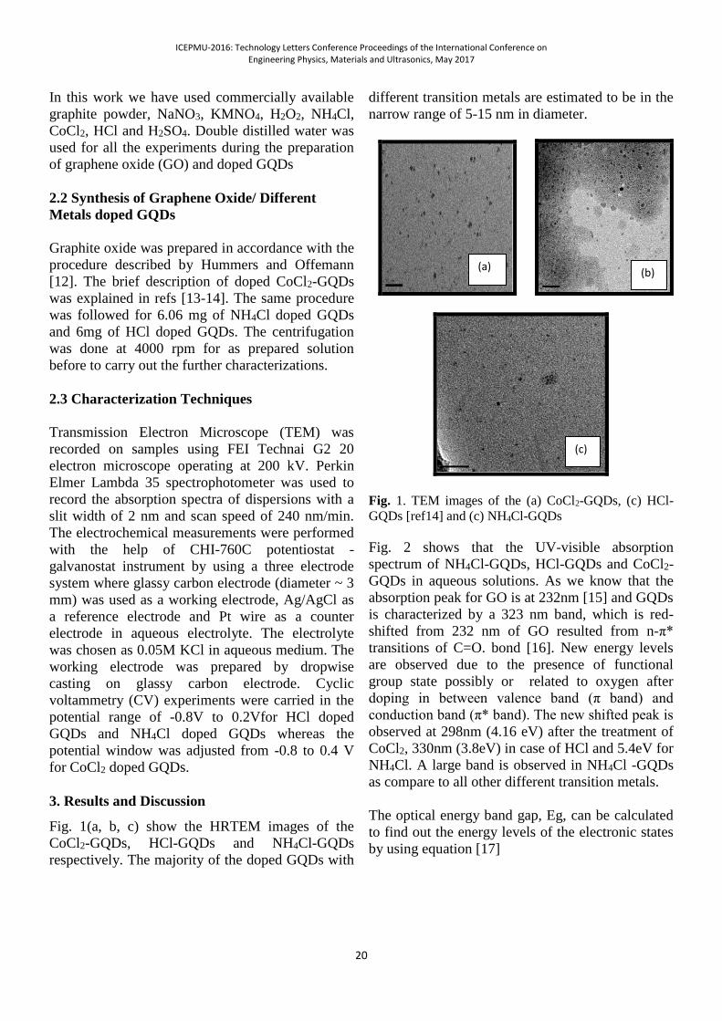
Fig. 1(a, b, c) show the HRTEM images of the
CoCl2-GQDs, HCl-GQDs and NH4Cl-GQDs
respectively. The majority of the doped GQDs with
different transition metals are estimated to be in the
narrow range of 5-15 nm in diameter.
50 nm
50 nm
Fig. 1. TEM images of the (a) CoCl2-GQDs, (c) HCl-
GQDs [ref14] and (c) NH4Cl-GQDs
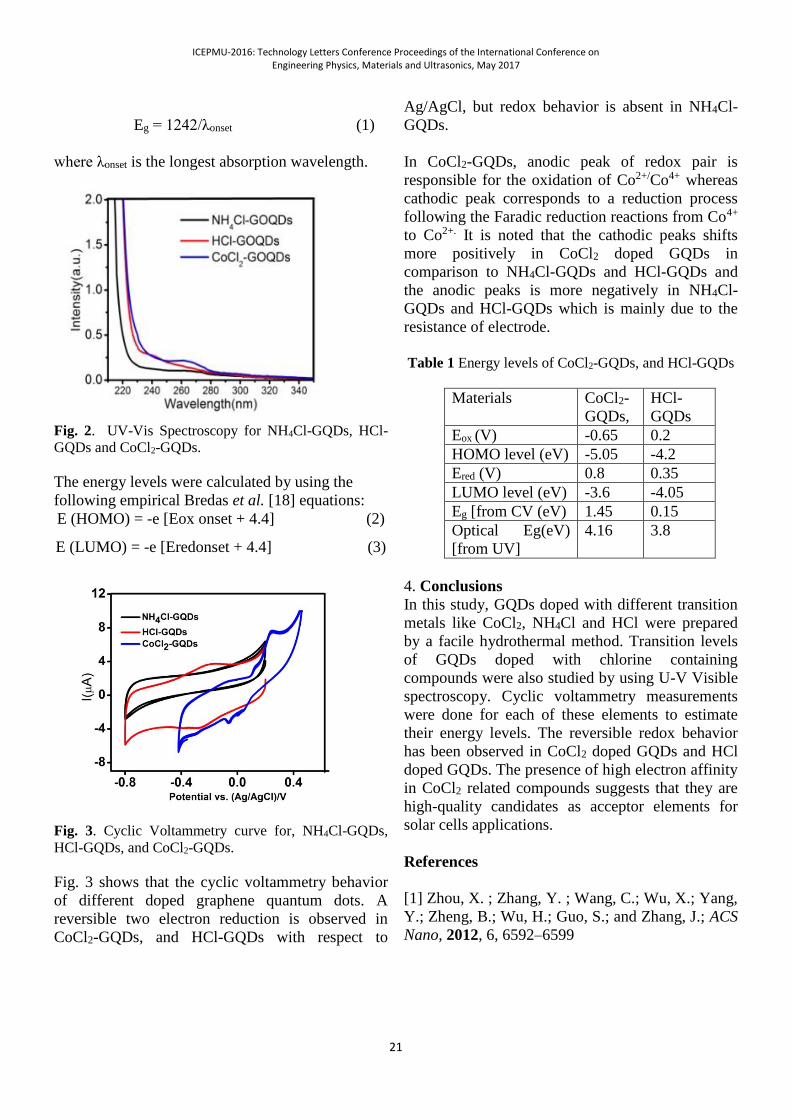
Fig. 2 shows that the UV-visible absorption
spectrum of NH4Cl-GQDs, HCl-GQDs and CoCl2-
GQDs in aqueous solutions. As we know that the
absorption peak for GO is at 232nm [15] and GQDs
is characterized by a 323 nm band, which is red-
shifted from 232 nm of GO resulted from n-π*
transitions of C=O. bond [16]. New energy levels
are observed due to the presence of functional
group state possibly or related to oxygen after
doping in between valence band (π band) and
conduction band (π* band). The new shifted peak is
observed at 298nm (4.16 eV) after the treatment of
CoCl2, 330nm (3.8eV) in case of HCl and 5.4eV for
NH4Cl. A large band is observed in NH4Cl -GQDs
as compare to all other different transition metals.
The optical energy band gap, Eg, can be calculated
to find out the energy levels of the electronic states
by using equation [17]
(a) (b)
(c)
ICEPMU-2016: Technology Letters Conference Proceedings of the International Conference on Engineering Physics, Materials and Ultrasonics, May 2017
21
Eg = 1242/λonset (1)
where λonset is the longest absorption wavelength.
Fig. 2. UV-Vis Spectroscopy for NH4Cl-GQDs, HCl-
GQDs and CoCl2-GQDs.
The energy levels were calculated by using the
following empirical Bredas et al. [18] equations:
E (HOMO) = -e [Eox onset + 4.4] (2)
E (LUMO) = -e [Eredonset + 4.4] (3)
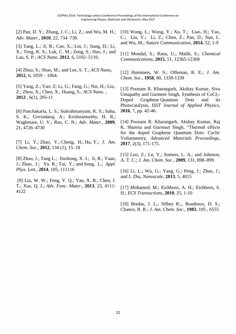
Fig. 3. Cyclic Voltammetry curve for, NH4Cl-GQDs,
HCl-GQDs, and CoCl2-GQDs.
Fig. 3 shows that the cyclic voltammetry behavior
of different doped graphene quantum dots. A
reversible two electron reduction is observed in
CoCl2-GQDs, and HCl-GQDs with respect to
Ag/AgCl, but redox behavior is absent in NH4Cl-
GQDs.
In CoCl2-GQDs, anodic peak of redox pair is
responsible for the oxidation of Co2+/Co4+ whereas
cathodic peak corresponds to a reduction process
following the Faradic reduction reactions from Co4+
to Co2+. It is noted that the cathodic peaks shifts
more positively in CoCl2 doped GQDs in
comparison to NH4Cl-GQDs and HCl-GQDs and
the anodic peaks is more negatively in NH4Cl-
GQDs and HCl-GQDs which is mainly due to the
resistance of electrode.
Table 1 Energy levels of CoCl2-GQDs, and HCl-GQDs
Materials CoCl2-
GQDs,
HCl-
GQDs
Eox (V) -0.65 0.2
HOMO level (eV) -5.05 -4.2
Ered (V) 0.8 0.35
LUMO level (eV) -3.6 -4.05
Eg [from CV (eV) 1.45 0.15
Optical Eg(eV)
[from UV]
4.16 3.8
4. Conclusions
In this study, GQDs doped with different transition
metals like CoCl2, NH4Cl and HCl were prepared
by a facile hydrothermal method. Transition levels
of GQDs doped with chlorine containing
compounds were also studied by using U-V Visible
spectroscopy. Cyclic voltammetry measurements
were done for each of these elements to estimate
their energy levels. The reversible redox behavior
has been observed in CoCl2 doped GQDs and HCl
doped GQDs. The presence of high electron affinity
in CoCl2 related compounds suggests that they are
high-quality candidates as acceptor elements for
solar cells applications.
References
[1] Zhou, X. ; Zhang, Y. ; Wang, C.; Wu, X.; Yang,
Y.; Zheng, B.; Wu, H.; Guo, S.; and Zhang, J.; ACS
Nano, 2012, 6, 6592–6599
ICEPMU-2016: Technology Letters Conference Proceedings of the International Conference on Engineering Physics, Materials and Ultrasonics, May 2017
22
[2] Pan, D. Y.; Zhang, J. C.; Li, Z.; and Wu, M. H.;
Adv. Mater., 2010, 22, 734–738.
[3] Tang, L.; Ji, R.; Cao, X.; Lin, J.; Jiang, H.; Li,
X.; Teng, K. S.; Luk, C. M.; Zeng, S.; Hao, J.; and
Lau, S. P.; ACS Nano, 2012, 6, 5102–5110.
[4] Zhuo, S.; Shao, M.; and Lee, S. T.; ACS Nano,
2012, 6, 1059 – 1064.
[5] Yang, Z.; Yao; Z; Li, G.; Fang, G.; Nie, H.; Liu,
Z.; Zhou, X.; Chen, X., Huang, S.; ACS Nano. ,
2012 , 6(1), 205-11
[6] Panchakarla, L. S.; Subrahmanyam, K. S.; Saha,
S. K.; Govindaraj, A.; Krishnamurthy, H. R.;
Waghmare, U. V.; Rao, C. N.; Adv. Mater., 2009,
21, 4726–4730
[7] Li, Y.; Zhao, Y.; Cheng, H.; Hu, Y.; J. Am.
Chem. Soc., 2012, 134 (1), 15–18
[8] Zhao, J.; Tang L.; Jinzhong, X. J.; Ji, R.; Yuan,
J.; Zhao, J.; Yu R.; Tai, Y.; and Song, L.; Appl.
Phys. Lett., 2014, 105, 111116
[9] Liu, W. W.; Feng, Y. Q.; Yan, X. B.; Chen, J.
T.; Xue, Q. J.; Adv. Func. Mater., 2013, 23, 4111-
4122
[10] Wang, L.; Wang, Y.; Xu, T.; Liao, H.; Yao,
C.; Liu, Y.; Li, Z.; Chen, Z.; Pan, D.; Sun, L.
and Wu, M.; Nature Communication, 2014, 52, 1-9
[11] Mondal, S.; Rana, U.; Malik, S.; Chemical
Communications, 2015, 51, 12365-12368
[12] Hummers, W. S.; Offeman, R. E.; J. Am.
Chem. Soc., 1958, 80, 1339-1339
[13] Poonam R. Kharangarh, Akshay Kumar, Siva
Umapathy and Gurmeet Singh, Synthesis of CoCl2-
Doped Graphene Quantum Dots and its
Photocatalysis, ISST Journal of Applied Physics,
2016, 7, pp. 42-46.
[14] Poonam R. Kharangarh, Akshay Kumar, Raj
K. Sharma and Gurmeet Singh, “Thermal effects
for the doped Graphene Quantum Dots: Cyclic
Voltammetry, Advanced Materials Proceedings,
2017, 2(3), 171-175.
[15] Luo, Z.; Lu, Y.; Somers, L. A.; and Johnson,
A. T. C.; J. Am. Chem. Soc., 2009, 131, 898–899.
[16] Li, L.; Wu, G.; Yang, G.; Peng, J.; Zhao, J.;
and J. Zhu, Nanoscale, 2013, 5, 4015
[17] Mohamed, M.; Eichborn, A. H.; Eichborn, S.
H.; ECS Transactions, 2010, 25, 1-10
[18] Bredas, J. L.; Silbey R.;, Boudreux, D. S.;
Chance, R. R.; J. Am. Chem. Soc., 1983, 105 , 6555
ICEPMU-2016: Technology Letters Conference Proceedings of the International Conference on Engineering Physics, Materials and Ultrasonics, May 2017
23
Electromagnetic Wave
Propagation in Photonic
Structures: Dielectric
and Metallo-Dielectric
Waveguides
Triranjita Srivastava, Pushpa Bindal*, Priyanka,
Anuradha, Priyam and Priscilla
Department of Physics, Kalindi College (University
of Delhi), Delhi, India, 110008
*Corresponding Author:
Abstract: The photonic waveguides are the vital
elements of integrated optics. In this paper, we
present the analysis of the electromagnetic wave
propagation in dielectric and few metallo-dielectric
waveguides. We present the universal V~b curves
and the modal fields for both TE and TM modes for
dielectric waveguide. The metallo-dielectric
waveguides comprise of various combinations of
metal and dielectric materials. The propagation
characteristics of basic metallo-dielectric
waveguides have been studied. We believe that
present work will enhance physical understanding
of the electromagnetic wave propagation through
various photonic waveguides.
Key words: Dielectric waveguides, Metallo-
Dielectric waveguides, Surface Plasmon Polaritons.
1. Introduction
The increasing demand of faster and huge data
transportation and processing has resulted into a
tremendous surge in developmental activities of
electronics and photonics. The electronic circuit
elements are now a days realized as small sized
functional devices such as mobiles, televisions,
computers, etc. but, they prevent the processor
speed above few Gb/s [1]. On the other hand, the
photonic interconnects, such as optical fibers offer
ultra-fast and large information carrying capacity
(Tb/s). Unfortunately, the photonic devices are
limited in size by the diffraction limit of about half
the wavelength of light (~ submicron), and tend to
be at least two orders larger than that of the
electronic components [2]. This size-mismatch
between the electronic and the photonic
components has been overcome by the study of
propagation of surface modes in the metallo-
dielectric waveguides [3].
In this paper, we present the propagation
characteristics of planar dielectric as well as few be
metallo dielectric waveguides, which can be
realized at subwavelength scale. The modal analysis
for the evaluation of propagation constant and the
modal fields for both TE and TM modes have been
done for dielectric waveguides. Moreover, SPP
modes have been studied for two types of basic
metallo-dielectric waveguides, namely; dielectric
layer between metal on either side (MDM) and
metal layer between dielectric on either side (DMD)
waveguides.
2. Mathematical Description
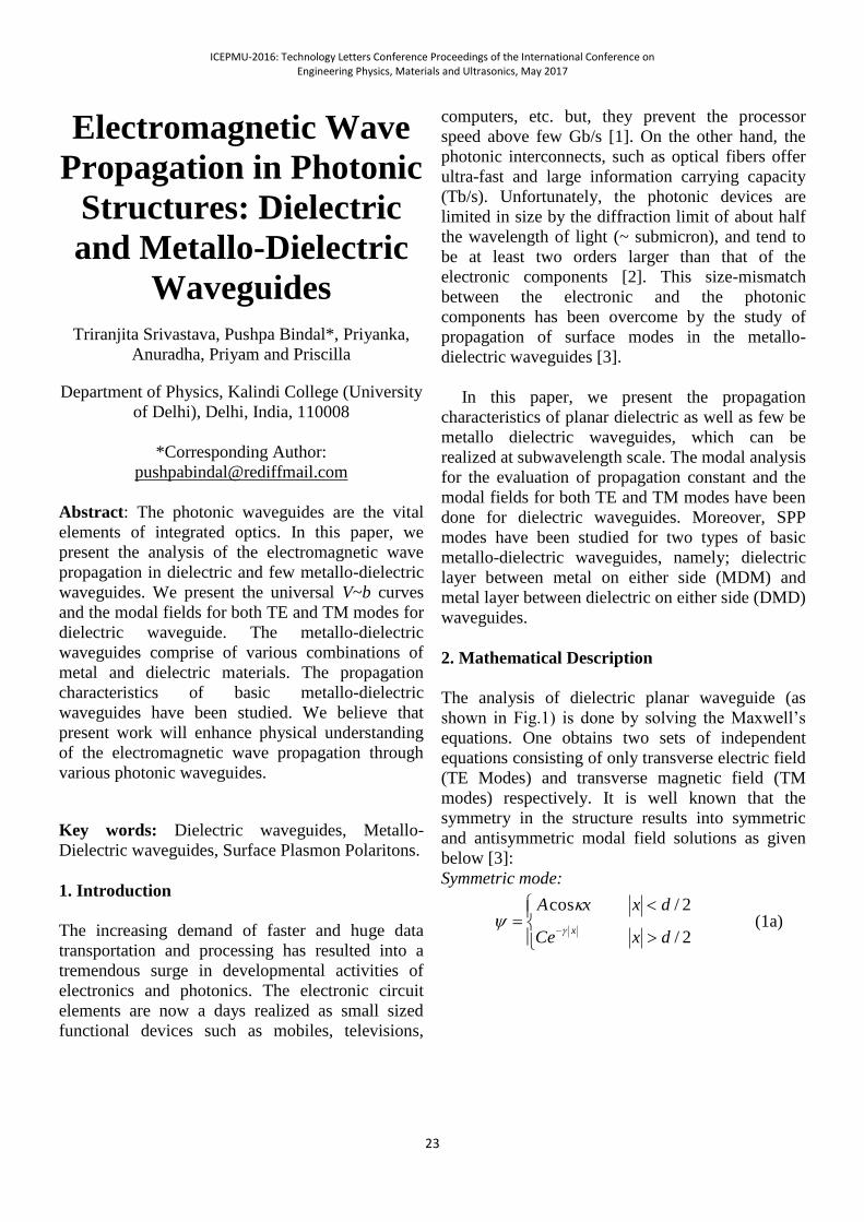
The analysis of dielectric planar waveguide (as
shown in Fig.1) is done by solving the Maxwell’s
equations. One obtains two sets of independent
equations consisting of only transverse electric field
(TE Modes) and transverse magnetic field (TM
modes) respectively. It is well known that the
symmetry in the structure results into symmetric
and antisymmetric modal field solutions as given
below [3]:
Symmetric mode:
2/
2/cos
dxCe
dxxA
x
(1a)
ICEPMU-2016: Technology Letters Conference Proceedings of the International Conference on Engineering Physics, Materials and Ultrasonics, May 2017
24
Antisymmetric mode:
2/
2/sin
dxCe
dxxA
x
(1b)
where 22
1
2
0 nk , 2
2
2
0
2 nk , A and C
are the constants to be determined. It is to be
mentioned that, the non-vanishing field components
for TE are Hx, Ey and Hz, whereas for TM
modes,
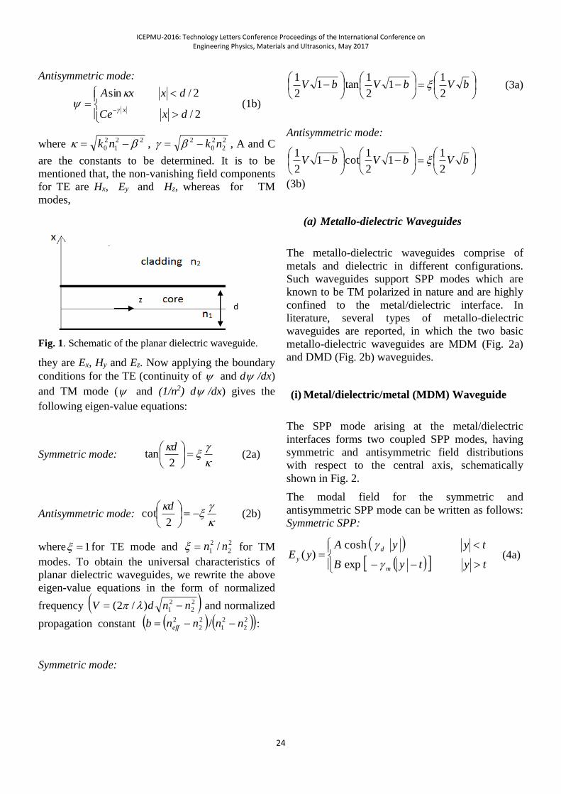
Fig. 1. Schematic of the planar dielectric waveguide.
they are Ex, Hy and Ez. Now applying the boundary
conditions for the TE (continuity of and d /dx)
and TM mode ( and (1/n2) d /dx) gives the
following eigen-value equations:
Symmetric mode:
2tan
d (2a)
Antisymmetric mode:
2cot
d (2b)
where 1 for TE mode and 2
2
2
1 / nn for TM
modes. To obtain the universal characteristics of
planar dielectric waveguides, we rewrite the above
eigen-value equations in the form of normalized
frequency 2
2
2
1)/2( nndV and normalized
propagation constant 2
2
2
1
2
2
2 / nnnnb eff :
Symmetric mode:
bVbVbV
2
11
2
1tan1
2
1 (3a)
Antisymmetric mode:
bVbVbV
2
11
2
1cot1
2
1
(3b)
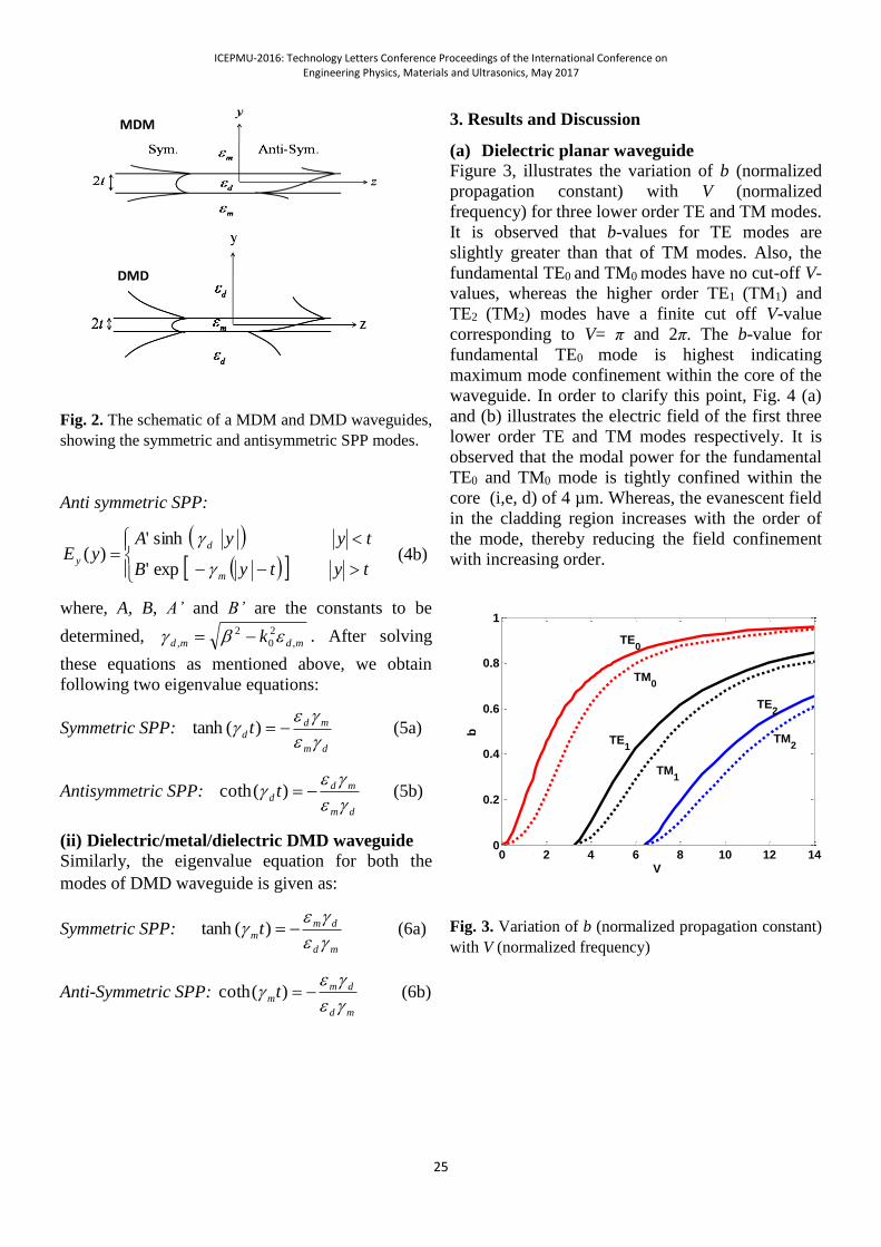
(a) Metallo-dielectric Waveguides
The metallo-dielectric waveguides comprise of
metals and dielectric in different configurations.
Such waveguides support SPP modes which are
known to be TM polarized in nature and are highly
confined to the metal/dielectric interface. In
literature, several types of metallo-dielectric
waveguides are reported, in which the two basic
metallo-dielectric waveguides are MDM (Fig. 2a)
and DMD (Fig. 2b) waveguides.
(i) Metal/dielectric/metal (MDM) Waveguide
The SPP mode arising at the metal/dielectric
interfaces forms two coupled SPP modes, having
symmetric and antisymmetric field distributions
with respect to the central axis, schematically
shown in Fig. 2.
The modal field for the symmetric and
antisymmetric SPP mode can be written as follows:
Symmetric SPP:
tytyB
tyyAyE
m
d
y
exp
cosh)( (4a)
z d
ICEPMU-2016: Technology Letters Conference Proceedings of the International Conference on Engineering Physics, Materials and Ultrasonics, May 2017
25
Fig. 2. The schematic of a MDM and DMD waveguides,
showing the symmetric and antisymmetric SPP modes.
Anti symmetric SPP:
tytyB
tyyAyE
m
d
y
exp'
sinh')( (4b)
where, A, B, A’ and B’ are the constants to be
determined, mdmd k ,
2
0
2
, . After solving
these equations as mentioned above, we obtain
following two eigenvalue equations:
Symmetric SPP: dm
mdd t
)(tanh (5a)
Antisymmetric SPP: dm
mdd t
)(coth (5b)
(ii) Dielectric/metal/dielectric DMD waveguide
Similarly, the eigenvalue equation for both the
modes of DMD waveguide is given as:
Symmetric SPP: md
dmmt
)(tanh (6a)
Anti-Symmetric SPP: md
dmmt
)(coth (6b)
3. Results and Discussion
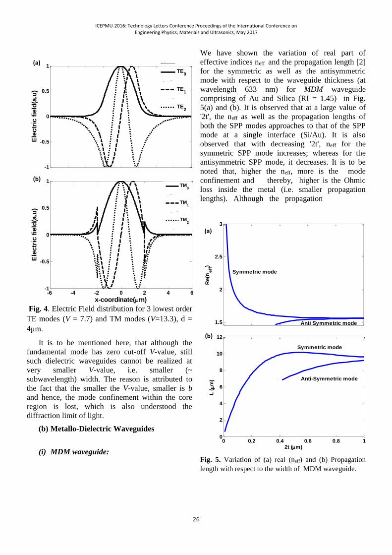
(a) Dielectric planar waveguide
Figure 3, illustrates the variation of b (normalized
propagation constant) with V (normalized
frequency) for three lower order TE and TM modes.
It is observed that b-values for TE modes are
slightly greater than that of TM modes. Also, the
fundamental TE0 and TM0 modes have no cut-off V-
values, whereas the higher order TE1 (TM1) and
TE2 (TM2) modes have a finite cut off V-value
corresponding to V= π and 2π. The b-value for
fundamental TE0 mode is highest indicating
maximum mode confinement within the core of the
waveguide. In order to clarify this point, Fig. 4 (a)
and (b) illustrates the electric field of the first three
lower order TE and TM modes respectively. It is
observed that the modal power for the fundamental
TE0 and TM0 mode is tightly confined within the
core (i,e, d) of 4 µm. Whereas, the evanescent field
in the cladding region increases with the order of
the mode, thereby reducing the field confinement
with increasing order.
0 2 4 6 8 10 12 140
0.2
0.4
0.6
0.8
1
V
b
TM1
TE0
TM0
TE1
TE2
TM2
Fig. 3. Variation of b (normalized propagation constant)
with V (normalized frequency)
MDM
DMD
ICEPMU-2016: Technology Letters Conference Proceedings of the International Conference on Engineering Physics, Materials and Ultrasonics, May 2017
26
-8 -6 -4 -2 0 2 4 6 8-1
-0.5
0
0.5
1
x-coordinate(m)
Ele
ctr
ic f
ield
(a.u
)
TE0
TE1
TE2
-6 -4 -2 0 2 4 6-1
-0.5
0
0.5
1
x-coordinate(m)
Ele
ctr
ic f
ield
(a.u
)
TM
0
TM1
TM2
Fig. 4. Electric Field distribution for 3 lowest order
TE modes (V = 7.7) and TM modes (V=13.3), d =
4μm.
It is to be mentioned here, that although the
fundamental mode has zero cut-off V-value, still
such dielectric waveguides cannot be realized at
very smaller V-value, i.e. smaller (~
subwavelength) width. The reason is attributed to
the fact that the smaller the V-value, smaller is b
and hence, the mode confinement within the core
region is lost, which is also understood the
diffraction limit of light.
(b) Metallo-Dielectric Waveguides
(i) MDM waveguide:
We have shown the variation of real part of
effective indices neff and the propagation length [2]
for the symmetric as well as the antisymmetric
mode with respect to the waveguide thickness (at
wavelength 633 nm) for MDM waveguide
comprising of Au and Silica (RI = 1.45) in Fig.
5(a) and (b). It is observed that at a large value of
'2t', the neff as well as the propagation lengths of
both the SPP modes approaches to that of the SPP
mode at a single interface (Si/Au). It is also
observed that with decreasing '2t', neff for the
symmetric SPP mode increases; whereas for the
antisymmetric SPP mode, it decreases. It is to be
noted that, higher the neff, more is the mode
confinement and thereby, higher is the Ohmic
loss inside the metal (i.e. smaller propagation
lengths). Although the propagation
0 0.2 0.4 0.6 0.8 1
1.5
2
2.5
3
2t (m)
Re
(ne
ff)
Symmetric mode
Anti Symmetric mode
0 0.2 0.4 0.6 0.8 10
2
4
6
8
10
12
2t (m)
L (
m)
Symmetric mode
Anti-Symmetric mode
Fig. 5. Variation of (a) real (neff) and (b) Propagation
length with respect to the width of MDM waveguide.
(a)
(b)
(a)
(b)
ICEPMU-2016: Technology Letters Conference Proceedings of the International Conference on Engineering Physics, Materials and Ultrasonics, May 2017
27
length of both the modes are ~ few μm, still it is
sufficient for the nanoscale dimensions [1]. Also,
the symmetric SPP mode does not have cut-off
thickness, whereas the antisymmetric SPP mode has
finite cut-off thickness, indicating that the
symmetric SPP mode can be realized at a very
small waveguide thickness ~ few 10 nm, thereby
indicating the realization of highly miniaturized
waveguides.
(ii) DMD Waveguide:
In contrast to MDM waveguides, the DMD
structures possess a complementary behavior for
the symmetric and the anti-symmetric modes. Fig.
6 (a) and (b) illustrates the variation of the real part
of neff and propagation lengths of both the
symmetric and antisymmetric SPP modes with
respect to the metal stripe thickness '2t' (at
wavelength 633 nm) for DMD waveguide
comprising of Si/Au/Si. The figure shows that for
both the SPP modes there is no cut off thickness
and at larger values of '2t' the mode effective
indices of both the modes approach to that of the
SPP at the single metal/dielectric interface.
As the metal stripe thickness '2t' decreases, neff
for the symmetric SPP mode decreases whereas, for
0 0.05 0.1 0.15 0.2 0.25 0.3
1.5
1.6
1.7
1.8
1.9
2
2t (m)
Re(n
eff
) Anti-Symmetric mode
Symmetric mode
0 0.05 0.1 0.15 0.2 0.25 0.3
100
102
104
2t (m)
L (
m) Symmetric mode
Anti-Symmetric mode
Fig. 6. Variation of (a) real part of neff and (b)
Propagation length with respect to width of the DMD
waveguide.
the antisymmetric mode it increases. Therefore, the
anti-symmetric SPP mode is confined to the metal
stripe of very small thickness. The propagation
length of the symmetric mode is ~ few mm, which
is several orders higher than that of MDM
waveguides. It is to mention here that the DMD
waveguides are highly useful in sensing
applications, as the Ohmic loss inside the metal is
very low and the modal field has large spatial extent
in the dielectric region.
Thus the metallo-dielectric waveguides can support
SPP modes, which are confined to the
metal/dielectric interface at subwavelength.
However, such modes suffer ohmic loss due to the
presence of metal, but the propagation length ~ few
10 nm, which is sufficient for the miniature
structures.
4. Conclusions
In this work we present the modal characteristics of
the planar dielectric and the plasmonic waveguides.
The plot of normalized propagation constant b
Verses normalized frequency V, and the modal
field distributions are shown for dielectric
(a)
(b)
ICEPMU-2016: Technology Letters Conference Proceedings of the International Conference on Engineering Physics, Materials and Ultrasonics, May 2017
28
waveguides, which indicates that such waveguides
have a constraint on the waveguide dimension
being limited by the diffraction limit of light. In
contrast to this, the metallo-dielectric waveguides
based on SPP modes can be realized at the
subwavelength dimensions.
References
[1] M. L. Borngersma, R. Zia and J. A. Schuller,
“Plasmonics- the missing link between
nanoelectronics and microphotonics,” Appl.
Phys. 2007, A89, 221 - 223
[2] W. L Barnes, “Surface plasmon-polaritons
length scales: a route to sub-wavelength optics,”
J. Opt. A: Pure Appl. Opt., 2006, 8, S87 - S93
[3] S. I. Bozhevolnyi, “Effective-index modeling of
channel plasmon polaritons,” Opt. Express,
2006, 14, 9467-9476
[4] A. Ghatak and K. Thyagarajan, “Introduction to
Fiber Optics,” Cambridge University Press,
Cambridge (1998). Reprinted by Foundation
Books, New Delhi, 2008
[5] E. D. Palik, “Handbook of Optical Constant of
Solids”, New York: Academic, 1985.
Acknowledgements: We would like to thank the
National Academy of Sciences India-Delhi Chapter
and Kalindi College for the financial support.
ICEPMU-2016: Technology Letters Conference Proceedings of the International Conference on Engineering Physics, Materials and Ultrasonics, May 2017
29
A Comparative Study
of Numerical Methods
for Analysing Planar
Plasmonic Waveguides
Triranjita Srivastava, Pushpa Bindal*, Asmita
Deep# and Ashima Sharda#
Department of Physics, Kalindi College
(University of Delhi), Delhi, India, 110008 #B.Sc. (H) Physics IIIrd year, Kalindi College
*Corresponding Author:
Abstract: The analysis of planar dielectric
waveguides have been widely done by employing
analytical numerical methods for solving the eigen-
value equations derived from Maxwell’s equation.
However, the analysis of planar plasmonic
waveguides is cumbersome, as the eigen-value
equations are complex and the dielectric constant
of metals, in general, is complex in nature.
Newton-Raphson method is a well-known method
for solving the complex eigen-value equations. But,
this method has certain limitations. It is a bit
tedious as it needs function & its derivative
evaluation. In this paper, we propose a modified
bisection method to solve complex eigen-value
equation, which is found to be simple and robust.
This method iteratively, bisects an appropriate
interval containing the root and then selects a
subinterval within which the root exists. The
comparison shows that the number of iteration
required in bisection method is many times less
than that of Newton Raphson method for the same
initial approximation. However, the time elapsed in
the executing the modified bisection method is
slightly larger than that required in Newton
Raphson Method; still the proposed method has
certain advantages over Newton Raphson Method.
Thus we employ the proposed method for the
analysis of various plasmonics waveguides, such as
metal/dielectric/metal waveguides.
Key words: Numerical methods, plasmonic
waveguides, complex eigen-values.
1. Introduction
Numerical methods involve the analysis of
algorithms which are based on certain numerical
approximations for mathematical analysis of the
real problems. Hence, the numerical methods are
applied in all areas of science and engineering. In
particular, the analytical methods are employed for
the analysis of the planar photonic waveguides,
because they are simple to implement and provide
physical understanding of the electromagnetic
wave propagation in such waveguides. These
analytical methods comprise of solving the eigen-
value equations, which are well known in the
literature [1]. However, the application of such
method for the analysis of planar plasmonics
waveguides is cumbersome, as the eigen-value
equations become complex, due to complex
dielectric constant of metals [2]. Therefore, in the
absence of exact analytical methods, the modeling
of the plasmonic waveguides is carried out by
employing either numerical methods or semi-
analytical methods. The numerical techniques, such
as finite difference method, finite element method,
etc, are time consuming, rigorous and require high
computational memory. Such methods are
sometimes found to be unstable, because of the fine
mesh at the vicinity of the edges of the metal. On
the other hand, the approximate analytical methods,
although are less accurate, but are simple to
implement and give better physical understanding
of the problem such as, the effect of the respective
role of the various waveguide parameters like
waveguide shape, size and operating wavelength.
Thus, in this paper we discuss the numerical
methods to solve complex eigen-value equations.
Newton-Raphson method is a well-known
numerical method for solving the complex eigen-
value equations [3]. But, this method is a bit
tedious as it needs function and its derivative
evaluation and has certain limitations. In this paper,
we propose a modified bisection method to solve
complex eigen-value equation, which is found to be
very simple & robust as it iteratively, bisects an
interval & then determines a subinterval within
which the root exists. The comparison shows that
the number of iterations required in bisection
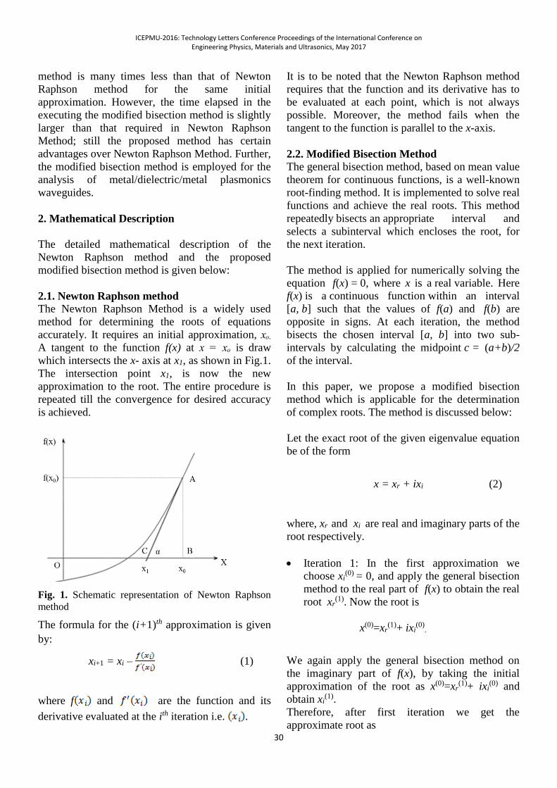
ICEPMU-2016: Technology Letters Conference Proceedings of the International Conference on Engineering Physics, Materials and Ultrasonics, May 2017
30
method is many times less than that of Newton
Raphson method for the same initial
approximation. However, the time elapsed in the
executing the modified bisection method is slightly
larger than that required in Newton Raphson
Method; still the proposed method has certain
advantages over Newton Raphson Method. Further,
the modified bisection method is employed for the
analysis of metal/dielectric/metal plasmonics
waveguides.
2. Mathematical Description
The detailed mathematical description of the
Newton Raphson method and the proposed
modified bisection method is given below:
2.1. Newton Raphson method
The Newton Raphson Method is a widely used
method for determining the roots of equations
accurately. It requires an initial approximation, xₒ.
A tangent to the function f(x) at x = xₒ is draw
which intersects the x- axis at x1, as shown in Fig.1.
The intersection point x1, is now the new
approximation to the root. The entire procedure is
repeated till the convergence for desired accuracy
is achieved.
Fig. 1. Schematic representation of Newton Raphson
method
The formula for the (i+1)th approximation is given
by:
xi+1 = xi – (1)
where f and are the function and its
derivative evaluated at the ith iteration i.e. .
It is to be noted that the Newton Raphson method
requires that the function and its derivative has to
be evaluated at each point, which is not always
possible. Moreover, the method fails when the
tangent to the function is parallel to the x-axis.
2.2. Modified Bisection Method
The general bisection method, based on mean value
theorem for continuous functions, is a well-known
root-finding method. It is implemented to solve real
functions and achieve the real roots. This method
repeatedly bisects an appropriate interval and
selects a subinterval which encloses the root, for
the next iteration.
The method is applied for numerically solving the
equation f(x) = 0, where x is a real variable. Here
f(x) is a continuous function within an interval
[a, b] such that the values of f(a) and f(b) are
opposite in signs. At each iteration, the method
bisects the chosen interval [a, b] into two sub-
intervals by calculating the midpoint c = (a+b)/2
of the interval.
In this paper, we propose a modified bisection
method which is applicable for the determination
of complex roots. The method is discussed below:
Let the exact root of the given eigenvalue equation
be of the form
x = xr + ixi (2)
where, xr and xi are real and imaginary parts of the
root respectively.
Iteration 1: In the first approximation we
choose xi(0) = 0, and apply the general bisection
method to the real part of f(x) to obtain the real
root xr(1). Now the root is
x(0)=xr(1)+ ixi
(0).
We again apply the general bisection method on
the imaginary part of f(x), by taking the initial
approximation of the root as x(0)=xr(1)+ ixi
(0) and
obtain xi(1).
Therefore, after first iteration we get the
approximate root as
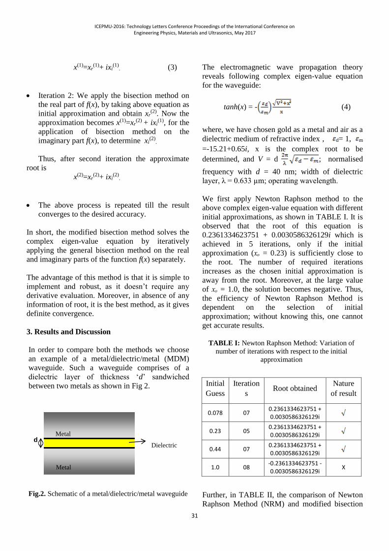
ICEPMU-2016: Technology Letters Conference Proceedings of the International Conference on Engineering Physics, Materials and Ultrasonics, May 2017
31
x(1)=xr(1)+ ixi
(1). (3)
Iteration 2: We apply the bisection method on
the real part of f(x), by taking above equation as
initial approximation and obtain xr(2). Now the
approximation becomes x(1)=xr(2) + ixi
(1), for the
application of bisection method on the
imaginary part f(x), to determine xi(2)
.
Thus, after second iteration the approximate
root is
x(2)=xr(2)+ ixi
(2).
The above process is repeated till the result
converges to the desired accuracy.
In short, the modified bisection method solves the
complex eigen-value equation by iteratively
applying the general bisection method on the real
and imaginary parts of the function f(x) separately.
The advantage of this method is that it is simple to
implement and robust, as it doesn’t require any
derivative evaluation. Moreover, in absence of any
information of root, it is the best method, as it gives
definite convergence.
3. Results and Discussion
In order to compare both the methods we choose
an example of a metal/dielectric/metal (MDM)
waveguide. Such a waveguide comprises of a
dielectric layer of thickness ‘d’ sandwiched
between two metals as shown in Fig 2.
Fig.2. Schematic of a metal/dielectric/metal waveguide
The electromagnetic wave propagation theory
reveals following complex eigen-value equation
for the waveguide:
tanh(x) = - (4)
where, we have chosen gold as a metal and air as a
dielectric medium of refractive index , d= 1, m
=-15.21+0.65i, x is the complex root to be
determined, and V = d ; normalised
frequency with d = 40 nm; width of dielectric
layer, λ = 0.633 µm; operating wavelength.
We first apply Newton Raphson method to the
above complex eigen-value equation with different
initial approximations, as shown in TABLE I. It is
observed that the root of this equation is
0.2361334623751 + 0.0030586326129i which is
achieved in 5 iterations, only if the initial
approximation (xₒ = 0.23) is sufficiently close to
the root. The number of required iterations
increases as the chosen initial approximation is
away from the root. Moreover, at the large value
of xₒ = 1.0, the solution becomes negative. Thus,
the efficiency of Newton Raphson Method is
dependent on the selection of initial
approximation; without knowing this, one cannot
get accurate results.
TABLE I: Newton Raphson Method: Variation of
number of iterations with respect to the initial
approximation
Initial
Guess
Iteration
s Root obtained
Nature
of result
0.078 07 0.2361334623751 + 0.0030586326129i
0.23 05 0.2361334623751 + 0.0030586326129i
0.44 07 0.2361334623751 + 0.0030586326129i
1.0 08 -0.2361334623751 -0.0030586326129i
X
Further, in TABLE II, the comparison of Newton
Raphson Method (NRM) and modified bisection
Metal
Dielectric
Metal d
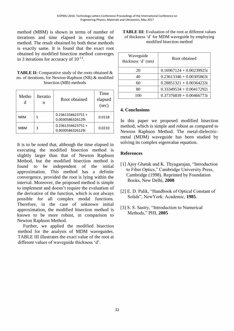
ICEPMU-2016: Technology Letters Conference Proceedings of the International Conference on Engineering Physics, Materials and Ultrasonics, May 2017
32
method (MBM) is shown in terms of number of
iterations and time elapsed in executing the
method. The result obtained by both these methods
is exactly same. It is found that the exact root
obtained by modified bisection method converges
in 3 iterations for accuracy of 10-13.
TABLE II: Comparative study of the roots obtained &
no. of iterations, for Newton-Raphson (NR) & modified
bisection (MB) methods
Metho
d
Iteratio
n Root obtained
Time
elapsed
(sec)
NRM 5 0.2361334623751 + 0.0030586326129i
0.0118
MBM 3 0.2361334623751 + 0.0030586326129i
0.0210
It is to be noted that, although the time elapsed in
executing the modified bisection method is
slightly larger than that of Newton Raphson
Method, but the modified bisection method is
found to be independent of the initial
approximation. This method has a definite
convergence, provided the root is lying within the
interval. Moreover, the proposed method is simple
to implement and doesn’t require the evaluation of
the derivative of the function, which is not always
possible for all complex modal functions.
Therefore, in the case of unknown initial
approximation, the modified bisection method is
known to be more robust, in comparison to
Newton Raphson Method.
Further, we applied the modified bisection
method for the analysis of MDM waveguides.
TABLE III illustrates the exact value of the root at
different values of waveguide thickness ‘d’.
TABLE III: Evaluation of the root at different values
of thickness ‘d’ for MDM waveguide by employing
modified bisection method
Waveguide
thickness ‘d’ (nm) Root obtained
20 0.16967124 + 0.00239925i
40 0.23613346 + 0.00305863i
60 0.28851321 + 0.00364233i
80 0.33349534 + 0.00417292i
100 0.37376839 + 0.00466773i
4. Conclusions
In this paper we proposed modified bisection
method, which is simple and robust as compared to
Newton Raphson Method. The metal-dielectric-
metal (MDM) waveguide has been studied by
solving its complex eigenvalue equation.
References
[1] Ajoy Ghatak and K. Thyagarajan, “Introduction
to Fiber Optics,” Cambridge University Press,
Cambridge (1998). Reprinted by Foundation
Books, New Delhi, 2008
[2] E. D. Palik, “Handbook of Optical Constant of
Solids”, NewYork: Academic, 1985.
[3] S. S. Sastry, “Introduction to Numerical
Methods,” PHI, 2005
ICEPMU-2016: Technology Letters Conference Proceedings of the International Conference on Engineering Physics, Materials and Ultrasonics, May 2017
33
STUDY OF
PROPAGATION
CHARACTERISTICS
OF OPTICAL
FIBERS:
EXPERIMENT AND
SIMULATION
Pushpa Bindal*, Triranjita Srivastava, Sujata#,
Anju# and Diksha Tandon#
Department of Physics, Kalindi College
(University of Delhi), Delhi, India, 110008 #B.Sc. (H) Physics IIIrd year, Kalindi College
*Corresponding Author:
Abstract: In this work, we present propagation
characteristics of fiber by employing simulations
and experiment. The variation of mode effective
index with respect to the wavelength is obtained
analytically by solving scalar wave equations. The
3-D modal field distribution and surface plots for
the first two lowest order LPlm modes are obtained.
Moreover, we experimentally employed the near
field scanning technique to obtain the diameter of
the core and refractive index variation in a
multimode optical fiber. It is observed that the
obtained results are in consensus with the given
specifications of optical fiber. We believe that the
present study will enhance the understanding of the
electromagnetic wave propagation in optical fibers.
Key words: Optical fiber, Refractive index profile,
Near field measurement technique.
1. Introduction
The increasing demand of faster and huge data
transportation, networking and processing has been
achieved only due to the very low transmission loss
(~0.2 dB/km) in optical fibers [1, 2]. The optical
fibers have found applications in data storing
equipment, telecommunication, medical use, oil
and gas industries, military, transport and also as
decorative material. Since few decades, there has
been a phenomenal growth in fiber optic industry,
which gave rise to various applications such as:
fiber optic sensors, integrated optic components
(polarizers, directional couplers, fiber gratings,
fiber amplifiers, optical switches, etc.) optical
signal processing, etc [3]. In addition to its
tremendous technological importance, fiber optics
also offers a platform to present demonstration and
understanding of various physical concepts.
We study the modal properties of optical fiber. The
variation of mode effective index has been
obtained for GeO2 doped optical fibers. We also
present the 3-D modal field distribution of two
lowest order modes, along with their 2-D surface
plots. It is to be mentioned here, that the modal
characteristics of fibers are almost dictated by the
refractive index variation in the core of the fiber.
Therefore, in this work we experimentally
employed near field scanning technique [4] to
determine the diameter and the refractive index
variation in the core of a given multimode optical
fiber. It has been observed that our results are
matching with the specifications of given optical
fiber.
2. Theory
The refractive index of the step-index optical fiber
(cross section shown in Fig. 1) is given by:
n(r)=
arn
arn
2
1 0 (1)
where n1 and n2 are the refractive indices of core
and cladding regions respectively, is the core
radius.
In order to obtain the propagation characteristics of
the optical fiber, we numerically solved the
Maxwell’s equations under weakly guiding
approximation.
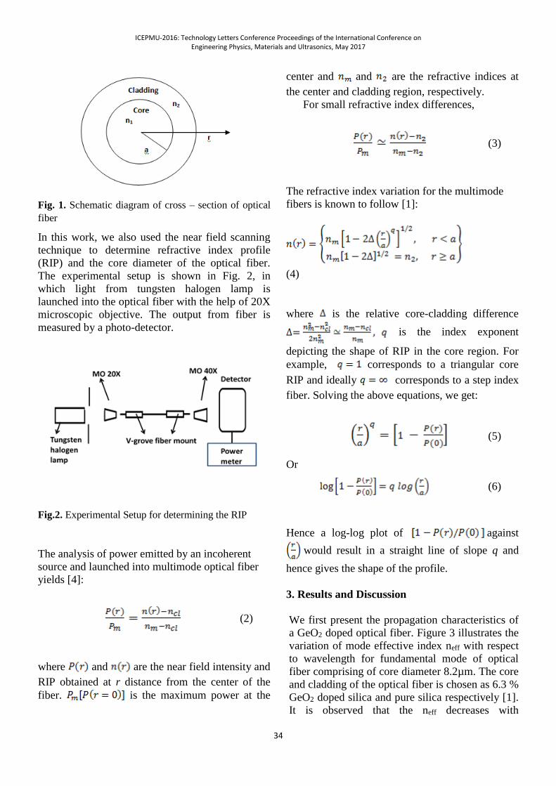
ICEPMU-2016: Technology Letters Conference Proceedings of the International Conference on Engineering Physics, Materials and Ultrasonics, May 2017
34
Fig. 1. Schematic diagram of cross – section of optical
fiber
In this work, we also used the near field scanning
technique to determine refractive index profile
(RIP) and the core diameter of the optical fiber.
The experimental setup is shown in Fig. 2, in
which light from tungsten halogen lamp is
launched into the optical fiber with the help of 20X
microscopic objective. The output from fiber is
measured by a photo-detector.
Fig.2. Experimental Setup for determining the RIP
The analysis of power emitted by an incoherent
source and launched into multimode optical fiber
yields [4]:
(2)
where and are the near field intensity and
RIP obtained at r distance from the center of the
fiber. is the maximum power at the
center and and are the refractive indices at
the center and cladding region, respectively.
For small refractive index differences,
(3)
The refractive index variation for the multimode
fibers is known to follow [1]:
(4)
where is the relative core-cladding difference
is the index exponent
depicting the shape of RIP in the core region. For
example, corresponds to a triangular core
RIP and ideally corresponds to a step index
fiber. Solving the above equations, we get:
(5)
Or
(6)
Hence a log-log plot of against
would result in a straight line of slope q and
hence gives the shape of the profile.
3. Results and Discussion
We first present the propagation characteristics of
a GeO2 doped optical fiber. Figure 3 illustrates the
variation of mode effective index neff with respect
to wavelength for fundamental mode of optical
fiber comprising of core diameter 8.2µm. The core
and cladding of the optical fiber is chosen as 6.3 %
GeO2 doped silica and pure silica respectively [1].
It is observed that the neff decreases with
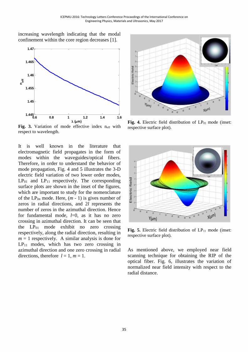
ICEPMU-2016: Technology Letters Conference Proceedings of the International Conference on Engineering Physics, Materials and Ultrasonics, May 2017
35
increasing wavelength indicating that the modal
confinement within the core region decreases [1].
0.6 0.8 1 1.2 1.4 1.61.445
1.45
1.455
1.46
1.465
1.47
(m)
ne
ff
Fig. 3. Variation of mode effective index neff with
respect to wavelength.
It is well known in the literature that
electromagnetic field propagates in the form of
modes within the waveguides/optical fibers.
Therefore, in order to understand the behavior of
mode propagation, Fig. 4 and 5 illustrates the 3-D
electric field variation of two lower order modes,
LP01 and LP11 respectively. The corresponding
surface plots are shown in the inset of the figures,
which are important to study for the nomenclature
of the LPlm mode. Here, (m - 1) is gives number of
zeros in radial directions, and 2l represents the
number of zeros in the azimuthal direction. Hence
for fundamental mode, l=0, as it has no zero
crossing in azimuthal direction. It can be seen that
the LP01 mode exhibit no zero crossing
respectively, along the radial direction, resulting in
m = 1 respectively. A similar analysis is done for
LP11 modes, which has two zero crossing in
azimuthal direction and one zero crossing in radial
directions, therefore l = 1, m = 1.
Fig. 4. Electric field distribution of LP01 mode (inset:
respective surface plot).
Fig. 5. Electric field distribution of LP11 mode (inset:
respective surface plot).
As mentioned above, we employed near field
scanning technique for obtaining the RIP of the
optical fiber. Fig. 6, illustrates the variation of
normalized near field intensity with respect to the
radial distance.
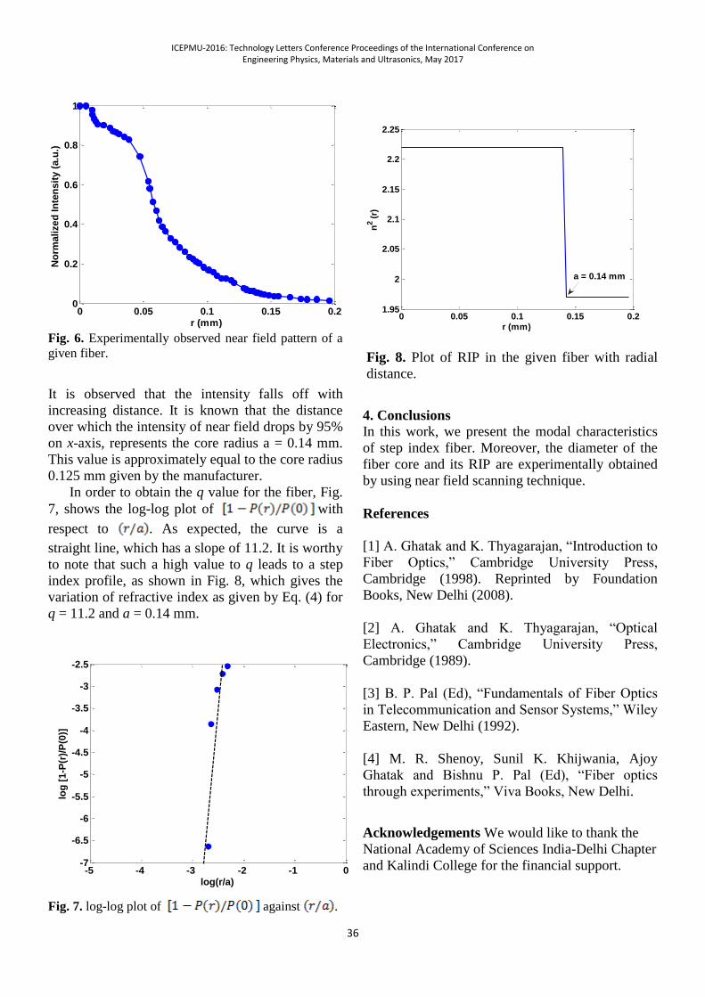
ICEPMU-2016: Technology Letters Conference Proceedings of the International Conference on Engineering Physics, Materials and Ultrasonics, May 2017
36
0 0.05 0.1 0.15 0.20
0.2
0.4
0.6
0.8
1
r (mm)
No
rmalized
In
ten
sit
y (
a.u
.)
Fig. 6. Experimentally observed near field pattern of a
given fiber.
It is observed that the intensity falls off with
increasing distance. It is known that the distance
over which the intensity of near field drops by 95%
on x-axis, represents the core radius a = 0.14 mm.
This value is approximately equal to the core radius
0.125 mm given by the manufacturer.
In order to obtain the q value for the fiber, Fig.
7, shows the log-log plot of with
respect to . As expected, the curve is a
straight line, which has a slope of 11.2. It is worthy
to note that such a high value to q leads to a step
index profile, as shown in Fig. 8, which gives the
variation of refractive index as given by Eq. (4) for
q = 11.2 and a = 0.14 mm.
-5 -4 -3 -2 -1 0-7
-6.5
-6
-5.5
-5
-4.5
-4
-3.5
-3
-2.5
log(r/a)
log
[1
-P(r
)/P
(0)]
Fig. 7. log-log plot of against .
0 0.05 0.1 0.15 0.21.95
2
2.05
2.1
2.15
2.2
2.25
r (mm)
n2 (
r)
a = 0.14 mm
Fig. 8. Plot of RIP in the given fiber with radial
distance.
4. Conclusions
In this work, we present the modal characteristics
of step index fiber. Moreover, the diameter of the
fiber core and its RIP are experimentally obtained
by using near field scanning technique.
References
[1] A. Ghatak and K. Thyagarajan, “Introduction to
Fiber Optics,” Cambridge University Press,
Cambridge (1998). Reprinted by Foundation
Books, New Delhi (2008).
[2] A. Ghatak and K. Thyagarajan, “Optical
Electronics,” Cambridge University Press,
Cambridge (1989).
[3] B. P. Pal (Ed), “Fundamentals of Fiber Optics
in Telecommunication and Sensor Systems,” Wiley
Eastern, New Delhi (1992).
[4] M. R. Shenoy, Sunil K. Khijwania, Ajoy
Ghatak and Bishnu P. Pal (Ed), “Fiber optics
through experiments,” Viva Books, New Delhi.
Acknowledgements We would like to thank the
National Academy of Sciences India-Delhi Chapter
and Kalindi College for the financial support.
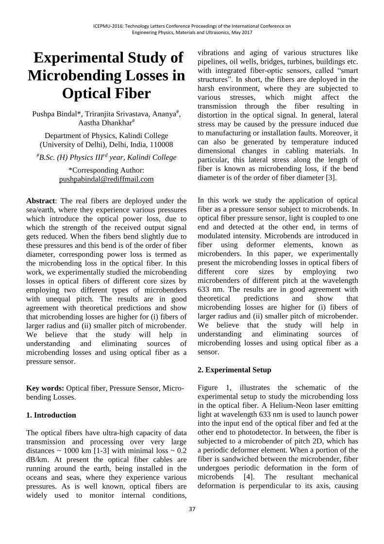
ICEPMU-2016: Technology Letters Conference Proceedings of the International Conference on Engineering Physics, Materials and Ultrasonics, May 2017
37
Experimental Study of
Microbending Losses in
Optical Fiber
Pushpa Bindal*, Triranjita Srivastava, Ananya#,
Aastha Dhankhar#
Department of Physics, Kalindi College
(University of Delhi), Delhi, India, 110008
#B.Sc. (H) Physics IIIrd year, Kalindi College
*Corresponding Author:
Abstract: The real fibers are deployed under the
sea/earth, where they experience various pressures
which introduce the optical power loss, due to
which the strength of the received output signal
gets reduced. When the fibers bend slightly due to
these pressures and this bend is of the order of fiber
diameter, corresponding power loss is termed as
the microbending loss in the optical fiber. In this
work, we experimentally studied the microbending
losses in optical fibers of different core sizes by
employing two different types of microbenders
with unequal pitch. The results are in good
agreement with theoretical predictions and show
that microbending losses are higher for (i) fibers of
larger radius and (ii) smaller pitch of microbender.
We believe that the study will help in
understanding and eliminating sources of
microbending losses and using optical fiber as a
pressure sensor.
Key words: Optical fiber, Pressure Sensor, Micro-
bending Losses.
1. Introduction
The optical fibers have ultra-high capacity of data
transmission and processing over very large
distances ~ 1000 km [1-3] with minimal loss ~ 0.2
dB/km. At present the optical fiber cables are
running around the earth, being installed in the
oceans and seas, where they experience various
pressures. As is well known, optical fibers are
widely used to monitor internal conditions,
vibrations and aging of various structures like
pipelines, oil wells, bridges, turbines, buildings etc.
with integrated fiber-optic sensors, called “smart
structures”. In short, the fibers are deployed in the
harsh environment, where they are subjected to
various stresses, which might affect the
transmission through the fiber resulting in
distortion in the optical signal. In general, lateral
stress may be caused by the pressure induced due
to manufacturing or installation faults. Moreover, it
can also be generated by temperature induced
dimensional changes in cabling materials. In
particular, this lateral stress along the length of
fiber is known as microbending loss, if the bend
diameter is of the order of fiber diameter [3].
In this work we study the application of optical
fiber as a pressure sensor subject to microbends. In
optical fiber pressure sensor, light is coupled to one
end and detected at the other end, in terms of
modulated intensity. Microbends are introduced in
fiber using deformer elements, known as
microbenders. In this paper, we experimentally
present the microbending losses in optical fibers of
different core sizes by employing two
microbenders of different pitch at the wavelength
633 nm. The results are in good agreement with
theoretical predictions and show that
microbending losses are higher for (i) fibers of
larger radius and (ii) smaller pitch of microbender.
We believe that the study will help in
understanding and eliminating sources of
microbending losses and using optical fiber as a
sensor.
2. Experimental Setup
Figure 1, illustrates the schematic of the
experimental setup to study the microbending loss
in the optical fiber. A Helium-Neon laser emitting
light at wavelength 633 nm is used to launch power
into the input end of the optical fiber and fed at the
other end to photodetector. In between, the fiber is
subjected to a microbender of pitch 2D, which has
a periodic deformer element. When a portion of the
fiber is sandwiched between the microbender, fiber
undergoes periodic deformation in the form of
microbends [4]. The resultant mechanical
deformation is perpendicular to its axis, causing
ICEPMU-2016: Technology Letters Conference Proceedings of the International Conference on Engineering Physics, Materials and Ultrasonics, May 2017
38
higher-order guided modes to radiate out of the
fibers core through the cladding interface.
Fig. 1. Micro-bending losses in Optical Fiber due to
pressure applied
When the pressure is applied to the microbender,
microbends are created which in turn modulate the
intensity of transmitted light at the other end of the
fiber. Higher order modes radiating out of fiber
core through core cladding interface due to external
pressure applied to the optical fiber perpendicular
to its axis, cause this fall in intensity of transmitted
light.
It is well known that the loss of guided power by
radiation at the bend is given by [5];
(1)
where ‘d’ represents the radius of core, ‘R’ is the
radius of curvature of bend, and A is a constant.
Thus, for a given fiber, the pressure applied to the
bend radius, which is given by
(2)
where, y is the displacement of fiber caused by
pressure in micro-bender element and 2D is the
distance between micro-bender element’s contact
points (pitch), as shown in Fig. 2.
Fig. 2. Geometry of the micro-bend
3. Results and Discussion
Fig. 3- 4, illustrates the variation of transmitted
intensity through a microbend modulated fiber
optic sensor with respect to the applied weight over
two types of microbenders namely; microbender 1
(pitch = 2.17 cm) and microbender 2 (pitch =
0.96cm). The chosen fiber is of core diameter 250
µm and 750 µm in fig. 3 and fig. 4 respectively. In
both the figures, as expected, the intensity
decreases parabolically with increasing weight.
Also the intensity is more for microbender 1, which
has larger pitch as compared to the microbender 2.
The reason attributed to the fact that larger the
pitch is, larger is the radius of curvature R (Eq. 2),
which results in decrease in transmission loss ,
hence we observe more transmitted intensity in the
case of microbender 1.
Figure 4, illustrates the similar variations in
transmitted intensity for the two microbenders for
fiber 2 of core diameter 750 µm. Clearly intensity
losses are higher for both microbenders since the
fiber has a larger diameter in comparison to fiber of
ICEPMU-2016: Technology Letters Conference Proceedings of the International Conference on Engineering Physics, Materials and Ultrasonics, May 2017
39
0 500 1000 1500 2000 25000
0.25
0.5
0.75
1
Weight (gm)
Inte
ns
ity
(a.u
)
microbender 1
microbender 2
Fig. 3. Variation of normalized intensity with respect to
weight applied at microbender 1 and microbender 2, for
fiber 1 of core diameter 250 µm.
Fig. 4. Variation of normalized intensity with respect to
weight applied at microbender 1 and microbender 2, for
fiber 2 of core diameter 750 µm.
Fig. 1, as expected. Further, Fig. 5 and 6, illustrate
the variation of normalized intensity with respect to
weight applied at microbender 1 and microbender
2, for two fibers; first fiber termed as fiber 1 has
core diameter of 250 µm and the second one called
fiber 2 with core diameter 750 µm. In both the
figures, it is observed that the transmitted intensity
falls off parabolically with respect to applied
weight. Moreover, fiber 1, which is of lesser
diameter as compared to fiber 2, exhibits low loss
and hence larger intensity. These findings can be
easily understood from Eq. (1).
0 500 1000 1500 2000 25000
0.2
0.4
0.6
0.8
1
Weight (gm)
Inte
nsit
y (
a.u
.)
Fiber 2
Fiber 1
Fig. 5. Variation of normalized intensity with respect to
weight applied at microbender 1 for two fibers; fiber 1
of core diameter 250 µm and fiber 2 of core diameter
750 µm.
0 500 1000 1500 20000
0.2
0.4
0.6
0.8
1
Weight (gm)
Inte
nsit
y (
a. u
.)
Fiber 1
Fiber 2
Fig. 6. Variation of normalized intensity with respect to
weight applied at microbender 2 for two fibers; fiber
1of core diameter 250 µm and fiber 2 of core diameter
750 µm.
Again losses are more in case of mirobender 2 in
Fig. 6 due to its smaller pitch. It is to be mentioned
here, that in Fig. 3-6, we employed quadratic curve
fitting of MATLAB®, which reveals parabolic fall
of intensity with respect to increase in weight.
In short, the results show good agreement with the
theoretical predictions of micro-bending losses.
ICEPMU-2016: Technology Letters Conference Proceedings of the International Conference on Engineering Physics, Materials and Ultrasonics, May 2017
40
The finding show that micro-bending losses are
higher for
(i) fibers of larger radius
(ii) smaller pitch of micro-bender.
4. Conclusions
In this paper we study the optical fiber pressure
sensor. The variation of transmitted intensity is
studied for two different micro-benders and
optical fibers. We believe that the study will help
in understanding and eliminating sources of
micro-bending losses and using optical fiber as a
sensor.
References
[1] A. Ghatak and K. Thyagarajan, “Introduction
to Fiber Optics,” Cambridge University Press,
Cambridge (1998). Reprinted by Foundation
Books, New Delhi, 2008
[2] A. Ghatak and K. Thyagarajan, “Optical
Electronics,” Cambridge University Press,
Cambridge, 1989
[3] B. P. Pal (Ed), “Fundamentals of Fiber Optics
in Telecommunication and Sensor Systems,”
Wiley Eastern, New Delhi, 1992
[4] M. R. Shenoy, Sunil K. Khijwania, Ajoy
Ghatak and Bishnu P. Pal (Ed), “Fiber optics
through experiments,” Viva Books, New Delhi.
[5] C. K. Kao, “Optical Fiber Systems:
Technology, design and application,” Mcgraw –
Hill, New York, 1982.
Acknowledgements
We would like to thank the National Academy of
Sciences India-Delhi Chapter and Kalindi
College for the financial support.
ICEPMU-2016: Technology Letters Conference Proceedings of the International Conference on Engineering Physics, Materials and Ultrasonics, May 2017
41
Growth of (001)
oriented Cr and MgO
thin films on
Amorphous Substrate
for Magnetic Tunnel
Junctions
Sajid Husain, and Sujeet Chaudhary*
Thin Film Laboratory, Department of Physics,
Indian Institute of Technology Delhi, New Delhi
110016 (INDIA)
Ankit Kumar, Serkan Akansel, and Peter
Svedlindh,
Ångström Laboratory, Department of Engineering
Sciences, Box 534, SE-751 21 Uppsala, Sweden
*Corresponding Author:
Abstract: We have carried out a systematic study
to optimize the growth parameters to obtain the
oriented growth of Cr (002) and MgO (200) thin
films using dual ion-beam sputtering technique on
thermally oxidized silicon and glass substrates. It is
found that the preferred crystallographic
orientation of Cr depends on the film growth rate
(sputtering rate) and its post annealing treatment.
X-ray diffraction analysis has revealed that 110 W
and 85 W grown and subsequently 500°C post
annealed Cr thin films result in the (110) and (002)
crystallographic orientations, respectively. The
MgO thin film grown at room temperature using
the oxygen ion assisted ion-beam sputter
deposition, without requiring any pre/post substrate
annealing treatment exhibits (200) orientation. The
interface/surface qualities of all the samples have
been investigated using X-ray reflectivity analysis.
Extremely small surface roughness of 0.28 and
1.49nm are observed for Cr and MgO films,
respectively. The oriented growth of MgO and Cr
thin films is established in correlation with the
energetic ion-beam deposition process which is
expedient in spintronic devices i.e., MTJs devices.
Key words: Cr, MgO, X-ray reflectivity 1.
1. Introduction
The chromium (Cr) and magnesium oxide (MgO)
thin films are pivotal choice of materials for
development of spintronics devices. Cr is one of
the inevitable choices of the buffer layer materials
for the growth of epitaxial ferromagnetic (FM)
layer particularly Co based Heusler alloy
(Co2FeAl) layer. However the MgO thin films not
only accommodating to induce perpendicular
magnetic anisotropy (PMA) but also inevitably
important as an insulator tunnel barrier for good
band matching with Heusler alloys [1]. This
suitable band matching among the FM Co2FeAl
(CFA) having low damping [2] and MgO layers
enhanced the electron tunnelling probability
consequently larger percentage change in magneto-
resistance ratio in magnetic tunnel junctions
(MTJs) devices. The MgO, alike Cr layer, is indeed
a choice of buffer layer materials to grow an
epitaxial Heusler alloy thin films [3]. It is well
known that the Cr thin films have either (110) or
(002) crystallographic texture. However, it is
difficult to grow (001) oriented Cr epitaxial layer
even on single crystal substrate [4]. To prevent
shunting to substrate in MTJs and spin transfer
torque (STT) spintronics devices it is indeed
needed to grow the epitaxial structures on
insulating substrates; particularly on the
technologically and industrially important
thermally oxidized silicon (Si/SiOx) substrate.
However the oriented growth on amorphous
substrate is technologically critical. To overcome
this issue we utilized energy enhanced ion beam
sputtering process to grow the Cr and MgO thin
films over (Si/SiOx) and glass substrates. In this
paper we report the growth rate dependency of the
orientation of Cr thin films, and oxygen ion
assisted 200 oriented stoichiometric phase
formation of MgO thin films.
2. Experimental
In this work the Cr thin films were deposited on
(Si/SiOx) substrates at 100W and 85W powers at
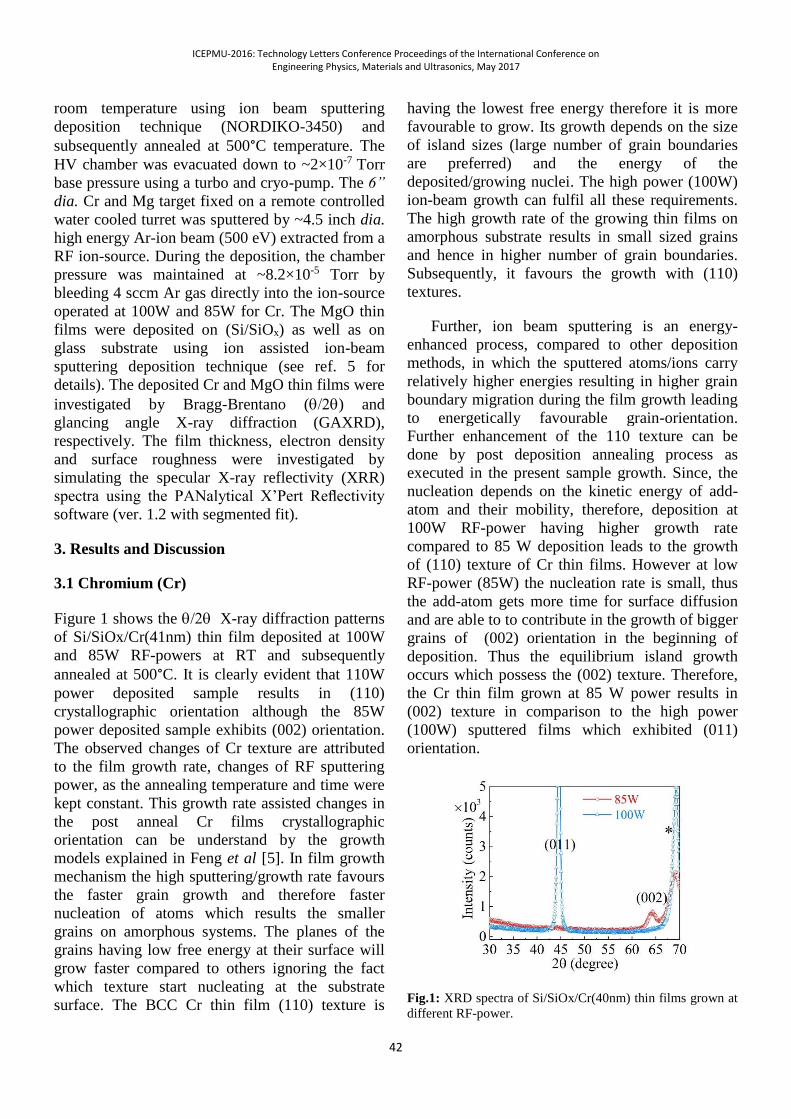
ICEPMU-2016: Technology Letters Conference Proceedings of the International Conference on Engineering Physics, Materials and Ultrasonics, May 2017
42
room temperature using ion beam sputtering
deposition technique (NORDIKO-3450) and
subsequently annealed at 500°C temperature. The
HV chamber was evacuated down to ~2×10⁻⁷ Torr
base pressure using a turbo and cryo-pump. The 6”
dia. Cr and Mg target fixed on a remote controlled
water cooled turret was sputtered by ~4.5 inch dia.
high energy Ar-ion beam (500 eV) extracted from a
RF ion-source. During the deposition, the chamber
pressure was maintained at ~8.2×10⁻⁵ Torr by
bleeding 4 sccm Ar gas directly into the ion-source
operated at 100W and 85W for Cr. The MgO thin
films were deposited on (Si/SiOx) as well as on
glass substrate using ion assisted ion-beam
sputtering deposition technique (see ref. 5 for
details). The deposited Cr and MgO thin films were
investigated by Bragg-Brentano () and
glancing angle X-ray diffraction (GAXRD),
respectively. The film thickness, electron density
and surface roughness were investigated by
simulating the specular X-ray reflectivity (XRR)
spectra using the PANalytical X’Pert Reflectivity
software (ver. 1.2 with segmented fit).
3. Results and Discussion
3.1 Chromium (Cr)
Figure 1 shows the X-ray diffraction patterns
of Si/SiOx/Cr(41nm) thin film deposited at 100W
and 85W RF-powers at RT and subsequently
annealed at 500°C. It is clearly evident that 110W
power deposited sample results in (110)
crystallographic orientation although the 85W
power deposited sample exhibits (002) orientation.
The observed changes of Cr texture are attributed
to the film growth rate, changes of RF sputtering
power, as the annealing temperature and time were
kept constant. This growth rate assisted changes in
the post anneal Cr films crystallographic
orientation can be understand by the growth
models explained in Feng et al [5]. In film growth
mechanism the high sputtering/growth rate favours
the faster grain growth and therefore faster
nucleation of atoms which results the smaller
grains on amorphous systems. The planes of the
grains having low free energy at their surface will
grow faster compared to others ignoring the fact
which texture start nucleating at the substrate
surface. The BCC Cr thin film (110) texture is
having the lowest free energy therefore it is more
favourable to grow. Its growth depends on the size
of island sizes (large number of grain boundaries
are preferred) and the energy of the
deposited/growing nuclei. The high power (100W)
ion-beam growth can fulfil all these requirements.
The high growth rate of the growing thin films on
amorphous substrate results in small sized grains
and hence in higher number of grain boundaries.
Subsequently, it favours the growth with (110)
textures.
Further, ion beam sputtering is an energy-
enhanced process, compared to other deposition
methods, in which the sputtered atoms/ions carry
relatively higher energies resulting in higher grain
boundary migration during the film growth leading
to energetically favourable grain-orientation.
Further enhancement of the 110 texture can be
done by post deposition annealing process as
executed in the present sample growth. Since, the
nucleation depends on the kinetic energy of add-
atom and their mobility, therefore, deposition at
100W RF-power having higher growth rate
compared to 85 W deposition leads to the growth
of (110) texture of Cr thin films. However at low
RF-power (85W) the nucleation rate is small, thus
the add-atom gets more time for surface diffusion
and are able to to contribute in the growth of bigger
grains of (002) orientation in the beginning of
deposition. Thus the equilibrium island growth
occurs which possess the (002) texture. Therefore,
the Cr thin film grown at 85 W power results in
(002) texture in comparison to the high power
(100W) sputtered films which exhibited (011)
orientation.
Fig.1: XRD spectra of Si/SiOx/Cr(40nm) thin films grown at
different RF-power.
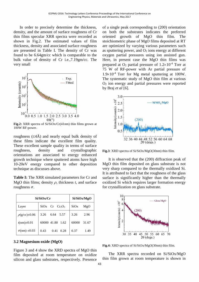
ICEPMU-2016: Technology Letters Conference Proceedings of the International Conference on Engineering Physics, Materials and Ultrasonics, May 2017
43
In order to precisely determine the thickness,
density, and the amount of surface roughness of Cr
thin films specular XRR spectra were recorded as
shown in Fig.2. The estimated values of film
thickness, density and associated surface roughness
are presented in Table I. The density of Cr was
found to be 6.64gm/cc which is comparable to the
bulk value of density of Cr i.e.,7.19gm/cc. The
very small
Fig.2: XRR spectra of Si/SiOx/Cr(41nm) thin films grown at
100W RF-power.
roughness (4Å) and nearly equal bulk density of
these films indicate the excellent film quality.
These excellent sample quality in terms of surface
roughness, density and crystallographic
orientations are associated to energy enhanced
growth technique where sputtered atoms have high
10-20eV energy compared to other deposition
technique as discusses above.
Table I: The XRR simulated parameters for Cr and
MgO thin films; density , thickness t, and surface
roughness .
Si/SiOx/Cr Si/SiOx/MgO
Layer SiOx Cr Cr2O3 SiOx MgO
(g/cc)±0.06 3.26 6.64 5.57 3.26 2.96
t(nm)±0.01 60000 41.80 1.62 60000 31.67
(nm) ±0.03 0.43 0.41 0.28 0.37 1.49
3.2 Magnesium oxide (MgO)
Figure 3 and 4 show the XRD spectra of MgO thin
film deposited at room temperature on oxidize
silicon and glass substrates, respectively. Presence
of a single peak corresponding to (200) orientation
on both the substrates indicates the preferred
oriented growth of MgO thin film. The
stoichiometric phase of MgO films deposited at RT
are optimized by varying various parameters such
as sputtering power, and O2 ions energy at different
oxygen partial pressures using ion assisted gun.
Here, in present case the MgO thin films was
prepared at O2 partial pressure of 1.210-4 Torr at
75 W of RF-power with Ar partial pressure of
1.910-4 Torr for Mg metal sputtering at 100W.
The systematic study of MgO thin film at various
O2 ion energy and partial pressures were reported
by Braj et al [6].
Fig.3: XRD spectra of Si/SiOx/MgO(30nm) thin film.
It is observed that the (200) diffraction peak of
MgO thin film deposited on glass substrate is not
very sharp compared to the thermally oxidized Si.
It is attributed to fact that the roughness of the glass
surface is significantly higher than the thermally
oxidized Si which requires larger formation energy
for crystallization on glass substrate.
Fig.4: XRD spectra of Si/SiOx/MgO(30nm) thin film.
The XRR spectra recorded on Si/SiOx/MgO
thin film grown at room temperature is shown in
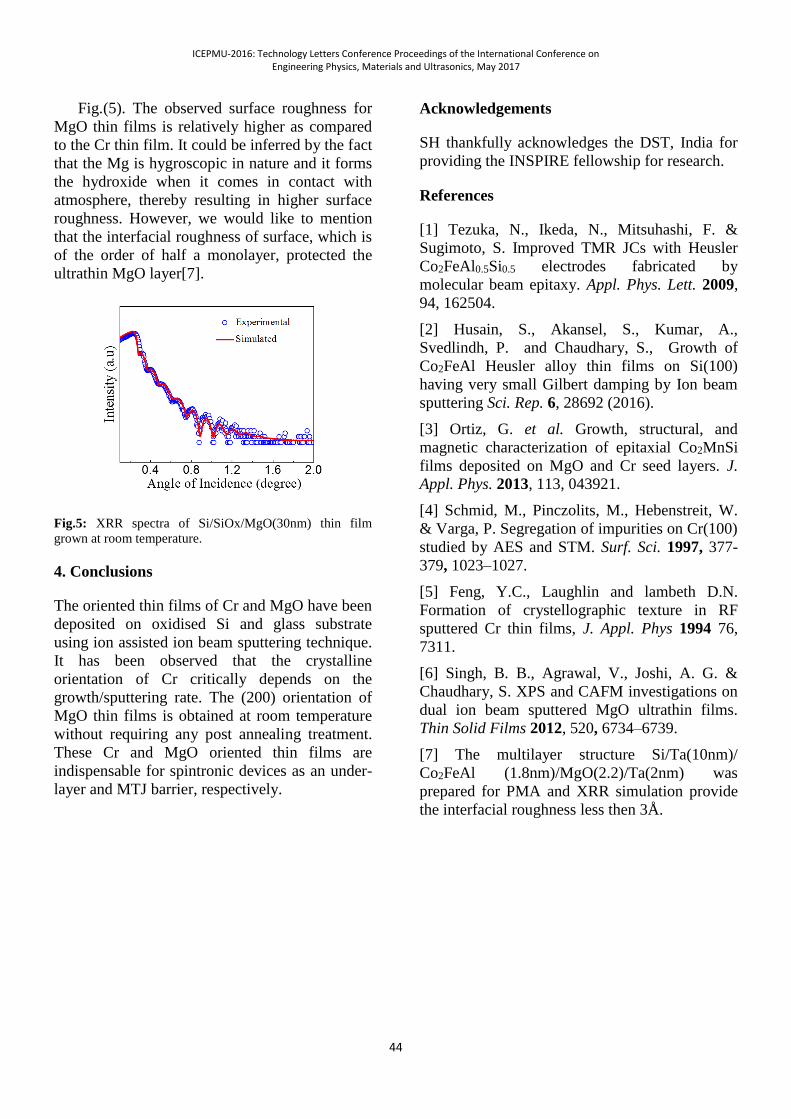
ICEPMU-2016: Technology Letters Conference Proceedings of the International Conference on Engineering Physics, Materials and Ultrasonics, May 2017
44
Fig.(5). The observed surface roughness for
MgO thin films is relatively higher as compared
to the Cr thin film. It could be inferred by the fact
that the Mg is hygroscopic in nature and it forms
the hydroxide when it comes in contact with
atmosphere, thereby resulting in higher surface
roughness. However, we would like to mention
that the interfacial roughness of surface, which is
of the order of half a monolayer, protected the
ultrathin MgO layer[7].
Fig.5: XRR spectra of Si/SiOx/MgO(30nm) thin film
grown at room temperature.
4. Conclusions
The oriented thin films of Cr and MgO have been
deposited on oxidised Si and glass substrate
using ion assisted ion beam sputtering technique.
It has been observed that the crystalline
orientation of Cr critically depends on the
growth/sputtering rate. The (200) orientation of
MgO thin films is obtained at room temperature
without requiring any post annealing treatment.
These Cr and MgO oriented thin films are
indispensable for spintronic devices as an under-
layer and MTJ barrier, respectively.
Acknowledgements
SH thankfully acknowledges the DST, India for
providing the INSPIRE fellowship for research.
References
[1] Tezuka, N., Ikeda, N., Mitsuhashi, F. &
Sugimoto, S. Improved TMR JCs with Heusler
Co2FeAl0.5Si0.5 electrodes fabricated by
molecular beam epitaxy. Appl. Phys. Lett. 2009,
94, 162504.
[2] Husain, S., Akansel, S., Kumar, A.,
Svedlindh, P. and Chaudhary, S., Growth of
Co2FeAl Heusler alloy thin films on Si(100)
having very small Gilbert damping by Ion beam
sputtering Sci. Rep. 6, 28692 (2016).
[3] Ortiz, G. et al. Growth, structural, and
magnetic characterization of epitaxial Co2MnSi
films deposited on MgO and Cr seed layers. J.
Appl. Phys. 2013, 113, 043921.
[4] Schmid, M., Pinczolits, M., Hebenstreit, W.
& Varga, P. Segregation of impurities on Cr(100)
studied by AES and STM. Surf. Sci. 1997, 377-
379, 1023–1027.
[5] Feng, Y.C., Laughlin and lambeth D.N.
Formation of crystellographic texture in RF
sputtered Cr thin films, J. Appl. Phys 1994 76,
7311.
[6] Singh, B. B., Agrawal, V., Joshi, A. G. &
Chaudhary, S. XPS and CAFM investigations on
dual ion beam sputtered MgO ultrathin films.
Thin Solid Films 2012, 520, 6734–6739.
[7] The multilayer structure Si/Ta(10nm)/
Co2FeAl (1.8nm)/MgO(2.2)/Ta(2nm) was
prepared for PMA and XRR simulation provide
the interfacial roughness less then 3Å.
ICEPMU-2016: Technology Letters Conference Proceedings of the International Conference on Engineering Physics, Materials and Ultrasonics, May 2017
45
Bio ceramics: Future
implant material
Aruna Dani
Asso. Prof. (App Physics) Priyadarshini College of
Engineering, Nagpur-440019, INDIA
Abstract: Ceramics exhibit many applications as
biomaterials due to their varied properties. Glass
ceramics possess many properties, similar to both
glass and ceramics as well. They have the property
of being inert in the human body. Because of their
quality of being hard and resistant to abrasion they
become the best option for tooth and bone
replacement. Some ceramics which are resistant to
friction, makes them useful as replacement
materials for malfunctioning joints. Aluminum
oxide has been used in orthopedic surgery for more
than 20 years as the joint replacement material due
to its exceptionally low coefficient of friction and
minimum wear and tare. Bioactive glasses are
composed of calcium and phosphate which are
present in a proportion that is similar to that of bone
in human body. These glasses bond to the tissue and
are biocompatible. They have large medical and
dental applications. Since bioactive glasses and
glass ceramics are brittle materials they are
specially used in the field of small bone defects.
Following inorganic processess occur when a
bioactive glass is immersed in a physiological
environment:
1. ion exchange
2. Hydrolysis
3. Condensation
4. Precipitation and
5. Mineralization.
This article reviews various properties of bioactive
glasses and their
applications
Keywords: Bioactive glasses, Bio Ceramics,
Implant material, biocompatible, Glass transition
1. Introduction: Bio ceramics are materials which
include Bio active glasses as well. They are a group
of glass ceramic materials having surface
reactivity. The biophysical properties of these
glasses has led them to be studied in detail to be
used as implant material. Ceramics show many
applications due to their physico-chemical
properties. They have the advantage of being
inactive in the human body. The resistance to
abrasion makes them useful for bones and tooth
replacement. A material is said to be bioactive, if it
gives an appropriate response to stmulii and results
in the formation of a bond between material and the
body tissue. Bioactive glasses are silicate based,
containing calcium and phosphate1.Hench was the
first to develop bioactive glasses, which were found
to able to bond to tissues2.The morphology of the
gel surface layer was a key point in determining the
response of bioactive glass . The ability of bonding
to bone also known as Biocompatibility was
increased for a certain compositions of bioactive
glasses.These bioactive glasses mainly contained
SiO2, Na2O, CaO and P2O5. Synthetic bone graft
material for general orthopaedics and dentistry are
some of the application of bioactive materials.
2. Experimental
2.1 Materials
Bioactive glasses are classified into different
groups and each group has a different
composition. Some bioactive glasses, for ex.
45S5, are now being used as bone grafting
material3. 45S5 bioactive glass is composed of SiO2
(46.1 mol%), CaO (26.9 mol%), Na2O (24.4 mol%)
and P2O5 (2.6 mol%)4 . 45S5 is able to form HCAP
(hydroxyl carbonated apatite) in less than 2 hours
and binds to tissues1. It is essential that a bioactive
glass forms without getting crystallized. If a
bioactive glass crystallizes, it becomes less
bioactive because the ion exchange between the
glass and aqueous solution is resisted by the
crystalline phases
2.2 Preparation of Samples: Bio active glasses
were initially obtained by the process of melting at
higher temperatures. The process for the
formation of bioactive glasses are melting at
ICEPMU-2016: Technology Letters Conference Proceedings of the International Conference on Engineering Physics, Materials and Ultrasonics, May 2017
46
Table Composition of bioactive glasses and glass
ceramics used for medical and dental applications
Composit
ion
Wt%
45S5
Bio
glass
S53P4 A-W glass
ceramic
Na2O 24.5 23 0
CaO 24.5 20 44.7
CaF2 0 0 0.5
MgO 0 0 4.6
P2O5 6 4 16.2
SiO2 45 53 34
Phases glass glass Beta-
wollstonite
glass
higher temperature and sol-gel. It was later
demonstrated that the formation of bioactive
glasses with a composition of SiO2- CaO-P2O5 by
sol-gel process was possible and it was also
observed that glasses were formed at lower
temperatures in sol-gel process as compared to
conventional melting method5,6.Glass transition
temperature (Tg), is a characteristic of any glass,
indicating a range of transformation when an
amorphous solid is changed into a super cooled
liquid on heating. In case of a bioactive glass a
linear relationship exists between Tg and hardness
of the glass. Reduction in Tg of a bioactive glass
indicates that the glass has reduced hardness.
3. Results and Discussion
Addition of fluoride increases re mineralization and
reduces demineralization. CaF2 concentration was
increased in SiO2-CaO-P2O5-Na2O system while
network connectivity was kept constant. It was
observed that due to addition of fluorine in
bioactive glass, there is decrease in Tg which means
that the glass has reduced hardness and is more
bioactive 7. For the prevention of caries, the role of
fluoride is very important. This substitution has a
profound effect on solubility of enamel8. As the
addition of fluoride is essential, its incorporation in
bioactive glasses is of immense importance. It was
observed that incorporation of fluorine in bioactive
glass, decreased its Tg which indicates that the glass
has reduced its hardness and is more bioactive.
Alternately, the onset of crystallization and peak
temperatures were decreased when CaF2 was
increased9 .
For example, when a particulate of bioactive glass
is used to fill a bone defect there is rapid
regeneration of bone that matches the architecture
and mechanical properties of bone at the site of
repair.
4. Conclusions Bioactive glasses with various
compositions are now used for wide range of
applications. Bioactive glasses have become an
area of interest for researchers from the field of
medicine and dentistry. The growing requirement
of tough, strong and stable bioinert glasses/
ceramics could be met either by nano-structured
ceramics or composites.
References
[1] Hench LL, Wilson J. An introduction to bio
ceramics. Singapore: World Scientific Publishing, 1993
[2] Hench LL. The story of Bioglass TM. J Mater Sci:
Mater Med 200617, 967-78
[3] Paolinelis G, Banarjee A, Watson TF. An in vitro
investigation of the effect and retention of bioactive
glass air-abrasive on sound and carious dentine. Journal
of Dentistry 2008,36,214-18
[4] Masahiro Kobayashi, Hiroaki Saito, Takatsune
Mase, Taketo Sasaki, Wei Wang, Yumi Tanaka, et al.
Polarization of hybridized calcium phospho
aluminosilicates with 45S5-type bioglasses. Biomed
Mater 2010 ,5,025001
[5] Rounan Li, Clarke, Hench. An investigation of bioactive glass powders by sol-gel processing. J Appl Biomater 1991,2(4), 231-39. [6] Peltola T, Jokinen M, Rahiala H, Levänen E,
Rosenholm, Kangasniemi, Yli-Urpo. Journal of
Biomedical Material Research 1999, 44(1), 12-21.
[7] Featherstone JDB. The science and practice of caries
prevention. J Am Dental Assoc JADA 2000, 131, 887-
99.
[8] Wei M, Evans JH, Bostrom T, Grondahl L. Syn-
thesis and characterization of hydroxyl apatite, fluoride-
substituted hydroxyl apatite and fluorapatite. J Mater
Sci Mater Med 2003, 14, 311-20.
[9] Brauer D, Karpukhina N, Law R, Hill R. Structure
of fluoride containing bioactive glasses. J Mater Chem
2009, 19,5629-36.
ICEPMU-2016: Technology Letters Conference Proceedings of the International Conference on Engineering Physics, Materials and Ultrasonics, May 2017
47
Intelligent
Transportation System
Shubham Sehgal, Akshat Mathur*, Mona
Aggrawal, Ram Sharma
Department of Electrical Electronics and
Communication Engineering
The NorthCap University, Gurgaon
Corresponding Author:
Abstract - With the emerging advancements in
transportation system, need for effective assistance
during this process has emerged. There is no
technology being used presently that assists
transportation through visible light. So we
discussed about Intelligent Transportation System
(ITS) that can be used as a potential element in
traffic control management. According to World
Health Organization’s figures, major cause of death
after the year 2000 are road accidents. VLC using
LED is technology which will help for high speed
and low cost wireless communication which will
be helpful in this study of Intelligent
Transportation System. The unique features and
benefits of VLC make it the most important
technological innovations in communication
system. In this paper we are discussing this concept
of Visible Light Communication to develop some
techniques in the field of transportation system.
Keywords – Visible Light Communication,
Vehicular Communication, Intelligent
Transportation System
1. Introduction
With the advent of smart technology in every field,
it is imperative to establish the transportation
system as smart, now considering the extent of
spread of transport network, a method needs to be
devised which can easily be used with the present
technology. The following texts focuses on
Intelligent Transportation System using Visible
Light. In Visible Light Communication (VLC),
communication takes place using visible light in
which LEDs perform two functions simultaneously
illumination and communication. ITS using visible
light would enable to use the light from the street
lights as a source to communicate. In VLC system,
modulation of intensity of light is done in such a
way that it is undetectable to human eye and have
no effect on the illumination functionality. LEDs
are used for transmission purpose because of its
certain advantages such as high lightening
efficiency, long durability, being environment
friendly and low power consumption. The
transmitter and receivers used have same
configuration as most of the general analog
communication systems as shown. LEDs are used
in head/tail lights of vehicles, street lights and
traffic lights which will make the deployment of
these Smart and Intelligent Transportation System
easy and using VLC technology. Using this
technology the vehicles will be able to
communicate about the speed, routes, destination,
and traffic conditions. Vehicular Communication
can be Vehicle to Vehicle, Vehicle to
Infrastructure, Infrastructure to Vehicle. Most
Challenging Project which is under consideration
of many scientist is development of Visible Light
Communication for Advanced Driver Assistance.
There are also many applications listed in this
paper like the Smart Obstacle Intimation System
[4], Blind Turn Assistance etc. Use of VLC in
Transportation System will be very advantageous
since it will make the transportation system faster,
easier and safer. ITS holds a promising sustainable
future , it can play a vital role in reducing pollution,
better traffic management and better on road
security. A great initiative has been taken in the
field of ITS.
2. Working
LEDs act as a transmitter as shown in diagram, the
transmitter and receiver configuration is similar to
the analog communication systems. Digital
Modulation Technique are used modulation of light
beam. Data transmission will be in binary form
since the two states of LED on and off can only
denote max two states. LED in on state will denote
binary ‘1’ similarly off state of LED will denote
binary ‘0’. At the receiver’s end we use a light
sensitive device like photodiodes for receiving this
encoded signal.
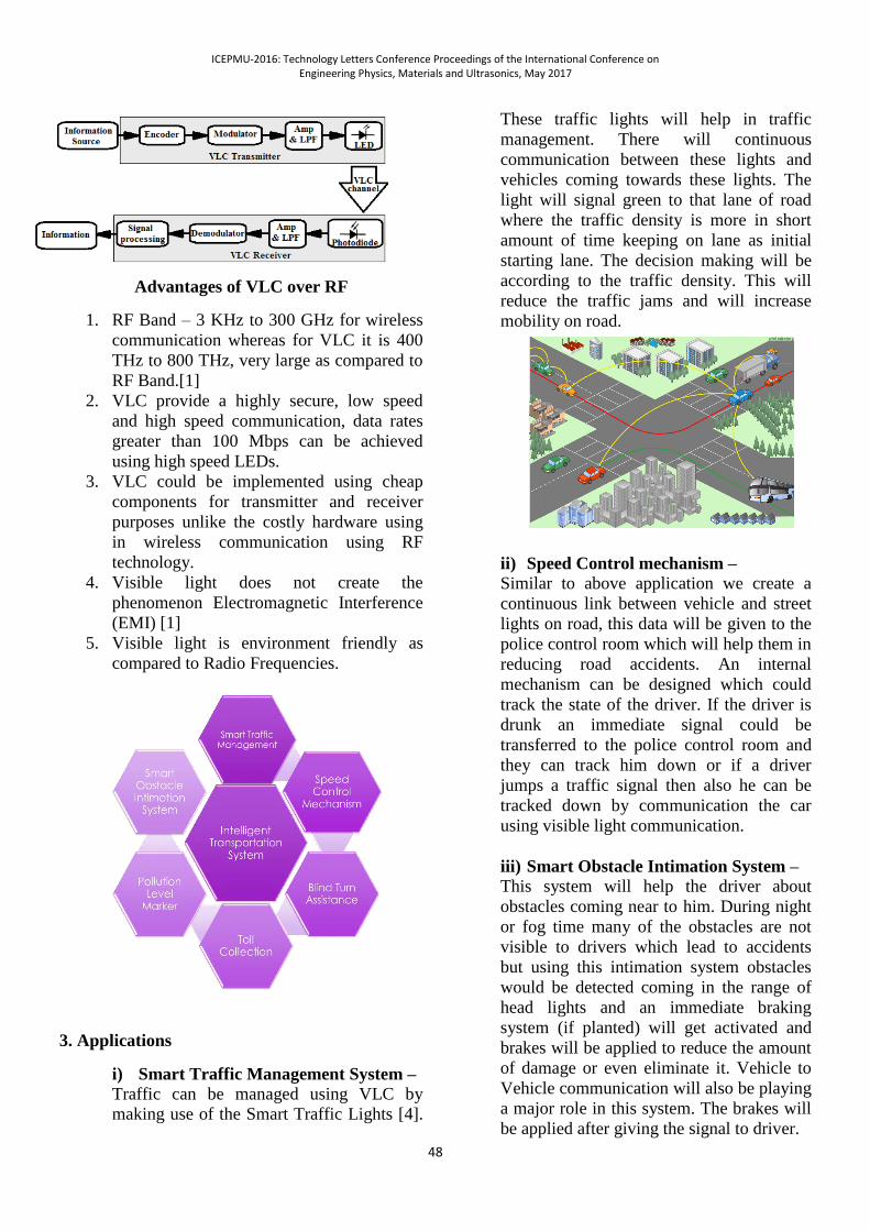
ICEPMU-2016: Technology Letters Conference Proceedings of the International Conference on Engineering Physics, Materials and Ultrasonics, May 2017
48
Advantages of VLC over RF
1. RF Band – 3 KHz to 300 GHz for wireless
communication whereas for VLC it is 400
THz to 800 THz, very large as compared to
RF Band.[1]
2. VLC provide a highly secure, low speed
and high speed communication, data rates
greater than 100 Mbps can be achieved
using high speed LEDs.
3. VLC could be implemented using cheap
components for transmitter and receiver
purposes unlike the costly hardware using
in wireless communication using RF
technology.
4. Visible light does not create the
phenomenon Electromagnetic Interference
(EMI) [1]
5. Visible light is environment friendly as
compared to Radio Frequencies.
3. Applications
i) Smart Traffic Management System –
Traffic can be managed using VLC by
making use of the Smart Traffic Lights [4].
These traffic lights will help in traffic
management. There will continuous
communication between these lights and
vehicles coming towards these lights. The
light will signal green to that lane of road
where the traffic density is more in short
amount of time keeping on lane as initial
starting lane. The decision making will be
according to the traffic density. This will
reduce the traffic jams and will increase
mobility on road.
ii) Speed Control mechanism –
Similar to above application we create a
continuous link between vehicle and street
lights on road, this data will be given to the
police control room which will help them in
reducing road accidents. An internal
mechanism can be designed which could
track the state of the driver. If the driver is
drunk an immediate signal could be
transferred to the police control room and
they can track him down or if a driver
jumps a traffic signal then also he can be
tracked down by communication the car
using visible light communication.
iii) Smart Obstacle Intimation System –
This system will help the driver about
obstacles coming near to him. During night
or fog time many of the obstacles are not
visible to drivers which lead to accidents
but using this intimation system obstacles
would be detected coming in the range of
head lights and an immediate braking
system (if planted) will get activated and
brakes will be applied to reduce the amount
of damage or even eliminate it. Vehicle to
Vehicle communication will also be playing
a major role in this system. The brakes will
be applied after giving the signal to driver.
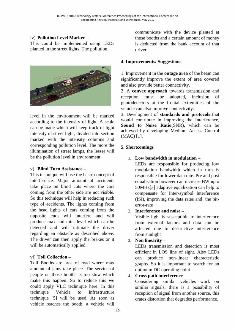
ICEPMU-2016: Technology Letters Conference Proceedings of the International Conference on Engineering Physics, Materials and Ultrasonics, May 2017
49
iv) Pollution Level Marker –
This could be implemented using LEDs
planted in the street lights. The pollution
level in the environment will be marked
according to the intensity of light. A scale
can be made which will keep track of light
intensity of street light, divided into section
marked with the intensity columns and
corresponding pollution level. The more the
illumination of street lamps, the lesser will
be the pollution level in environment.
v) Blind Turn Assistance –
This technique will use the basic concept of
interference. Major amount of accidents
take place on blind cuts where the cars
coming from the other side are not visible.
So this technique will help in reducing such
type of accidents. The lights coming from
the head lights of cars coming from the
opposite ends will interfere and will
produce max and min. level which can be
detected and will intimate the driver
regarding an obstacle as described above.
The driver can then apply the brakes or it
will be automatically applied.
vi) Toll Collection –
Toll Booths are area of road where max
amount of jams take place. The service of
people on those booths is too slow which
make this happen. So to reduce this we
could apply VLC technique here. In this
technique Vehicle to Infrastructure
technique [5] will be used. As soon as
vehicle reaches the booth, a vehicle will
communicate with the device planted at
those booths and a certain amount of money
is deducted from the bank account of that
driver.
4. Improvements/ Suggestions
1. Improvement in the outage area of the beam can
significantly improve the extent of area covered
and also provide better connectivity.
2. A convex approach towards transmission and
reception must be adopted, inclusion of
photodetectors at the frontal extremities of the
vehicle can also improve connectivity.
3. Development of standards and protocols that
would contribute in improving the Interference,
Sound to Noise Ratio(SNR), which can be
achieved by developing Medium Access Control
(MAC) [1].
5. Shortcomings
1. Low bandwidth in modulation –
LEDs are responsible for producing low
modulation bandwidth which in turn is
responsible for lower data rate. Pre and post
equalisation however can increase BW upto
50MHz[3] adaptive equalization can help to
compensate for Inter-symbol Interference
(ISI), improving the data rates and the bit-
error-rate
2. Interference and noise –
Visible light is susceptible to interference
from external factors and data can be
affected due to destructive interference
from sunlight
3. Non linearity –
LEDs transmission and detection is most
efficient in LOS line of sight. Also LEDs
can produce non-linear characteristic
graphs. So it is important to search for an
optimum DC operating point
4. Cross path interference –
Considering similar vehicles work on
similar signals, there is a possibility of
reception of signal from another source, this
crates distortion that degrades performance.
ICEPMU-2016: Technology Letters Conference Proceedings of the International Conference on Engineering Physics, Materials and Ultrasonics, May 2017
50
6. Conclusion
In this paper we mainly reviewed the
fundamentals and application of visible light
communication is the area of transportation. The
results of research done in the area of ITS have
been promising and ITS using VLC till now has
also proven to be an upcoming technology that
can benefit many areas of transportation like data
collection, toll collection, accidents safety etc.
and benefits include mobility, efficiency, safety
etc. With further research in this area VLC can
definitely replace DSRC in intelligent
transportation system. Many features provide
VLC in ITS an edge over other technologies most
importantly, unlike most emerging technologies,
cost of establishment with this would be much
less, since it can use the present infrastructure
References
[1]Navin Kumar “An Emerging Visible Light
Communication System for Driver Assistance”
[2] Kashif Naseer Qureshi and Abdul Hanan
Abdullah ” A Survey on Intelligent
Transportation Systems” Middle-East Journal of
Scientific Research 15 (5): 629-642, 2013
[3] Carlos Medina, Mayteé Zambrano and Kiara
Navarro “Led based visible light communication:
technology, applications and challenges – a
survey” International Journal of Advances in
Engineering & Technology, Aug., 2015.
[4] Navin Kumar “Visible Light Communication
in Intelligent Transportation Systems” IEEE
International Conference on Communications
[5]Anitha Chepuru , Dr.K.Venugopal Rao “A
Survey on IOT Applications for Intelligent
Transport Systems” Technical Research
Organization India