printed vs conventional electronics · printed vs conventional electronics . ... fr b3 i2 fr b3 i3...
TRANSCRIPT

Prof. Bruno Andò, University of Catania
Dip
arti
men
to d
i In
gegn
eria
Ele
ttri
ca, E
lett
ron
ica
e In
form
atic
a
Printed vs Conventional Electronics

Prof. Bruno Andò, University of Catania
Dip
arti
men
to d
i In
gegn
eria
Ele
ttri
ca, E
lett
ron
ica
e In
form
atic
a
Printed Electronics: Introduction
Printed Electronics
Printed Sensors
Inkjet Wearable electronics (Active clothing)
Smart Labels (RFID+sensors)
Disposable devices (biomedical) …
Low Costs/Good Performances
Flexible substrates

Prof. Bruno Andò, University of Catania
Dip
arti
men
to d
i In
gegn
eria
Ele
ttri
ca, E
lett
ron
ica
e In
form
atic
a
Technology Advantages Drawbacks
Screen Printing several materials complex multilayer
masks low resolution time consuming high cost production
Low cost Inkjet Printing
good resolution No masks rapid prototyping low cost system low cost production
restricted kinds of materials
Professional Inkjet Printing
high resolution several materials rapid prototyping Low cost production
high cost system
Mixed Screen & Inkjet Printing
good resolution several materials
masks time consuming high cost
Overview of Printing techniques
Rap
id p
roto
typ
ing Why rapid prototyping?
Application contexts • labscale prototype
• research laboratories
• educational activities
• customized devices

Prof. Bruno Andò, University of Catania
Dip
arti
men
to d
i In
gegn
eria
Ele
ttri
ca, E
lett
ron
ica
e In
form
atic
a
Electronics Engineering
Chemistry
Printed Electronics: Required Skills
Physics
MEMS & NEMS Technologies
Inks
Printing Sytems
Substrates
C
H
A
L
L
E
N
G
E
S
Before entering the market various technological improvements are still needed.
Prof. Bruno Andò, University of Catania
Dip
arti
men
to d
i In
gegn
eria
Ele
ttri
ca, E
lett
ron
ica
e In
form
atic
a
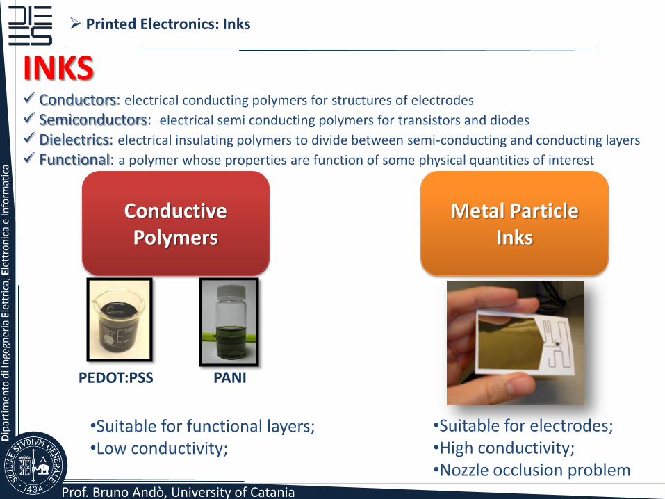
Printed Electronics: Inks
INKS Conductors: electrical conducting polymers for structures of electrodes
Semiconductors: electrical semi conducting polymers for transistors and diodes
Dielectrics: electrical insulating polymers to divide between semi-conducting and conducting layers
Functional: a polymer whose properties are function of some physical quantities of interest
Conductive Polymers
Metal Particle Inks
PEDOT:PSS PANI
•Suitable for functional layers; •Low conductivity;
•Suitable for electrodes; •High conductivity; •Nozzle occlusion problem

Prof. Bruno Andò, University of Catania
Dip
arti
men
to d
i In
gegn
eria
Ele
ttri
ca, E
lett
ron
ica
e In
form
atic
a
Università Degli Studi di Catania
Dip
arti
men
to d
i In
gegn
eria
Ele
ttri
ca, E
lett
ron
ica
e d
ei S
iste
mi
Inkjet Printing Systems
Everyday desktop printer Dimatix DMP 2800
www.dimatix.com
Microdrop inkjet system www.microdrop.de
Litrex M-Series inkjet system www.litrex.com
One Printing system for each application
context!!! Precision and accuracy Throughput/speed and productivity Maintenance and reliability Compatibility with electronic fluids Compatibility with the substrate

Prof. Bruno Andò, University of Catania
Dip
arti
men
to d
i In
gegn
eria
Ele
ttri
ca, E
lett
ron
ica
e In
form
atic
a
•Metalon® JS-B15P Water-based nano-Silver ink specially formulated for piezo inkjet printing methods.
-High conductivity -Compatible with porous substrates (PET)
•A commercial printer •Postprocessing
Low COST Technology
Resistivity 48 cm
Sheet Resistance 1600 m/
Viscosity 1-5 cps
Ag content 15%

Prof. Bruno Andò, University of Catania
Dip
arti
men
to d
i In
gegn
eria
Ele
ttri
ca, E
lett
ron
ica
e In
form
atic
a
Electron microscopy (SEM) inspection of electrodes with a track width of 200 m. A spacing of 150m does not assure tracks insulation.
Below 200 μm
Electrodes analysis
Over 200 μm
Electron microscopy (SEM) images of the silver layer deposited on the device. The silver layer is quite homogeneous. An approximated thickness of 1.90 µm has been estimated.
Prof. Bruno Andò, University of Catania
Dip
arti
men
to d
i In
gegn
eria
Ele
ttri
ca, E
lett
ron
ica
e In
form
atic
a
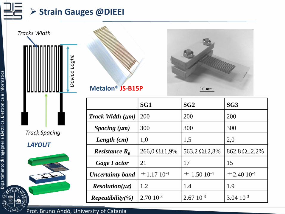
Strain Gauges @DIEEI
Dev
ice
Leg
ht
Tracks Width
Track Spacing
LAYOUT
SG1 SG2 SG3
Track Width (m) 200 200 200
Spacing (m) 300 300 300
Length (cm) 1,0 1,5 2,0
Resistance R0 266,0 1,9% 563,2 2,8% 862,8 2,2%
Gage Factor 21 17 15
Uncertainty band ±1.17 10-4 ± 1.50 10-4 ±2.40 10-4
Resolution() 1.2 1.4 1.9
Repeatibility(%) 2.70 10-3 2.67 10-3 3.04 10-3
Metalon® JS-B15P

Prof. Bruno Andò, University of Catania
Dip
arti
men
to d
i In
gegn
eria
Ele
ttri
ca, E
lett
ron
ica
e In
form
atic
a
LOW ACCELERATION LOW ACCELERATION
HIGH ACCELERATION
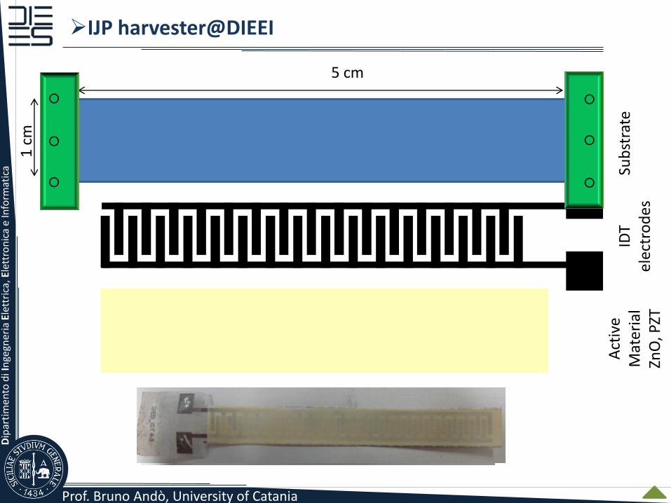
IJP Bistable Beam@DIEEI
IJP technology can be used to: •Validate simulations & models •Realize the device
1 cm
5 cm
A PET beam isused as substrate
L=10 cm W=1.5 cm ΔY=0.15 cm
A printed STRAIN GAUGE isused to convert the mechanicalsingnl into electricall signal
A CLAMP is usedto fix the beam
Non linear STB devices can be used to implement swicthes, harvesters,…..
Prof. Bruno Andò, University of Catania
Dip
arti
men
to d
i In
gegn
eria
Ele
ttri
ca, E
lett
ron
ica
e In
form
atic
a
1 c
m
5 cm
Sub
stra
te
IDT
elec
tro
des
Act
ive
M
ater
ial
ZnO
, PZT
IJP harvester@DIEEI

Prof. Bruno Andò, University of Catania
Dip
arti
men
to d
i In
gegn
eria
Ele
ttri
ca, E
lett
ron
ica
e In
form
atic
a
APPLICATION POINTS
1
2
3
4
5
1
2
3
4
5
0
5
10
15
20
25
30
distribuzione interpolata 3D
0
5
10
15
20
25
30
Testing the reliability of materials and prosthesys health,by monitoring the Tibio-Femoral stress.
MUX
IJP sensors for Bio-medical measurements@DIEEI

Prof. Bruno Andò, University of Catania
Dip
arti
men
to d
i In
gegn
eria
Ele
ttri
ca, E
lett
ron
ica
e In
form
atic
a
IJP Inclinometer@ DIEEI
0 1 2 3 4 5 6 7-2.5
-2
-1.5
-1
-0.5
0
0.5
1
1.5
2
2.5
Time (s)
Ou
tpu
t V
olt
ag
e (
V)
0 10 20 30 40 50 60 70 80 90
0
1
2
3
4
5
6
7
8
Tilt (°)
Ou
tpu
t V
olt
ag
e (
V)
experimental data
linear model

Prof. Bruno Andò, University of Catania
Dip
arti
men
to d
i In
gegn
eria
Ele
ttri
ca, E
lett
ron
ica
e In
form
atic
a
IJP Mass Sensor @DIEEI
1.9 cm
4.6
7 cm
0 0.05 0.1 0.15 0.2 0.25 0.3 0.355.5
6
6.5
7
7.5
8
8.5
9
9.5
10
10.5
11
Mass (g)
Fre
quency (
Hz)
Frequency trend (B3 fixed)
fr B3 I1
fr B3 I2
fr B3 I3
fr B3 I4
fr B3 I5
0 0.5 1 1.5 2 2.5 3 3.5 4-0.03
-0.02
-0.01
0
0.01
0.02
0.03
0.04
Time (s)
Voltage (
V)
Filtered impulse response (B1 I5 M0)
Impulse response operation
1 2 3 4 5
Current I
(mA)
20 30 40 50 60
Magnetic
field B (G)
2799 1606 945

Prof. Bruno Andò, University of Catania
Dip
arti
men
to d
i In
gegn
eria
Ele
ttri
ca, E
lett
ron
ica
e In
form
atic
a
Load sensor @ DIEEI
IDT Silver Ink
Rubber Dielectric Layer
PET SubstrateProtective Layer
PMMA Support
PET
Rubber layer
Tracks thickness: 200 nm Rubber thickness: 800 µm Rubber dielectric constant: 3 F/m. Protective layer thickness: 100 µm Assembled structure capacitance: 6 pF.

Prof. Bruno Andò, University of Catania
Dip
arti
men
to d
i In
gegn
eria
Ele
ttri
ca, E
lett
ron
ica
e In
form
atic
a
Realization of the load sensor
IDT Silver Ink
Rubber Dielectric Layer
PET SubstrateProtective Layer
PMMA Support
PET

Prof. Bruno Andò, University of Catania
Dip
arti
men
to d
i In
gegn
eria
Ele
ttri
ca, E
lett
ron
ica
e In
form
atic
a
Analog Readout Strategy
0 2.5 5 7.5 10 12.5 15 17.5 20 22.5 25 27.5 300.2
0.225
0.25
0.275
0.3
0.325
0.35
0.375
0.4
0.425
0.45
Measurement Samples (g)
Vo
ltag
e A
mp
litu
de
(V)
2508.00063.0 mV
This linear trend is justified by: •The linear relationship between the bridge output signal and the Strain •The linear relationship between the Strain and the Stress (load)
0.24 0.26 0.28 0.3 0.32 0.34 0.36 0.38 0.4 0.42 0.44-5
0
5
10
15
20
25
30
35
Ma
ss (
g)
Voltage Amplitude (V)
Prof. Bruno Andò, University of Catania
Dip
arti
men
to d
i In
gegn
eria
Ele
ttri
ca, E
lett
ron
ica
e In
form
atic
a
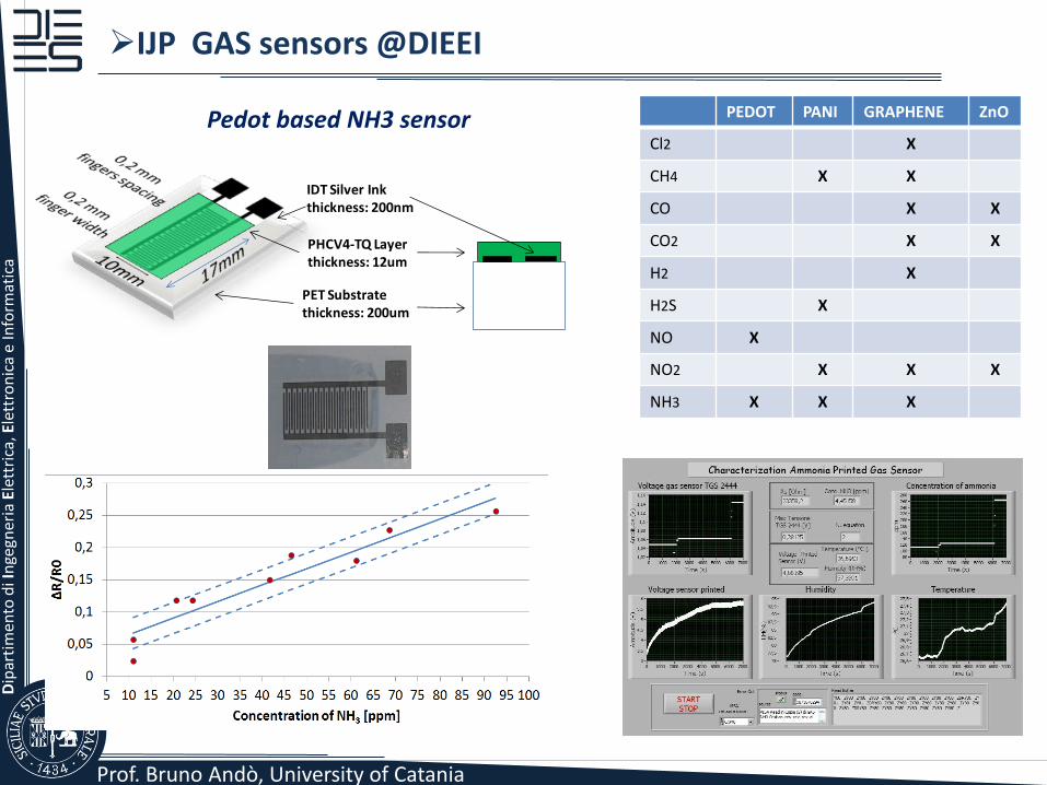
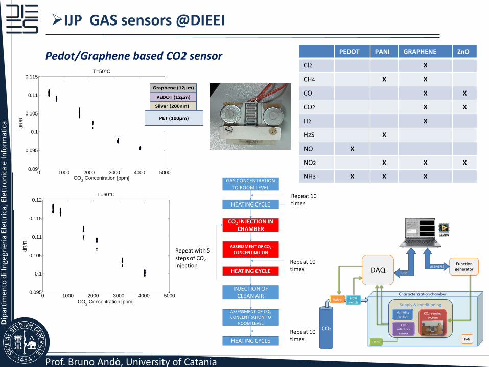
PEDOT PANI GRAPHENE ZnO
Cl2 X
CH4 X X
CO X X
CO2 X X
H2 X
H2S X
NO X
NO2 X X X
NH3 X X X
IJP GAS sensors @DIEEI
Pedot based NH3 sensor
IDT Silver Inkthickness: 200nm
PET Substratethickness: 200um
PHCV4-TQ Layerthickness: 12um
Prof. Bruno Andò, University of Catania
Dip
arti
men
to d
i In
gegn
eria
Ele
ttri
ca, E
lett
ron
ica
e In
form
atic
a
PEDOT PANI GRAPHENE ZnO
Cl2 X
CH4 X X
CO X X
CO2 X X
H2 X
H2S X
NO X
NO2 X X X
NH3 X X X
IJP GAS sensors @DIEEI
Pedot/Graphene based CO2 sensor
Supply & conditioning
Characterization chamber
DAQ
CO2
USB
Valve Flow switch
Functiongenerator
USB/GPIB
LM35
Humiditysensor
CO2
referencesensor
CO2 sensingsystem
FAN
0 1000 2000 3000 4000 50000.09
0.095
0.1
0.105
0.11
0.115T=50°C
CO2 Concentration [ppm]
dR
/R
0 1000 2000 3000 4000 50000.095
0.1
0.105
0.11
0.115
0.12T=60°C
CO2 Concentration [ppm]
dR
/R
Prof. Bruno Andò, University of Catania
Dip
arti
men
to d
i In
gegn
eria
Ele
ttri
ca, E
lett
ron
ica
e In
form
atic
a
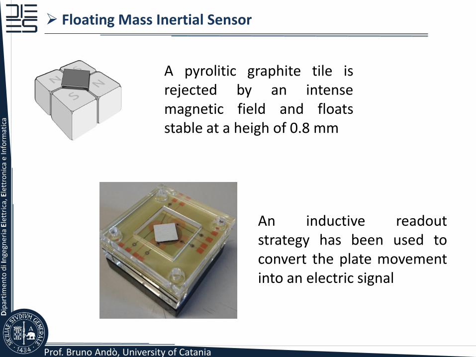
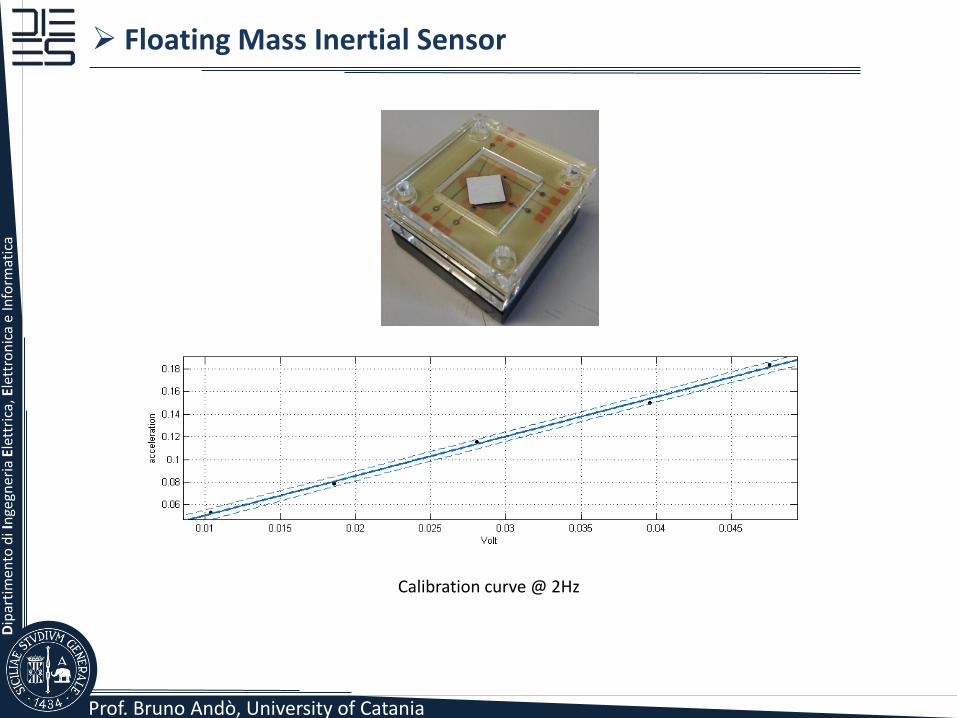
Floating Mass Inertial Sensor
A pyrolitic graphite tile is rejected by an intense magnetic field and floats stable at a heigh of 0.8 mm
An inductive readout strategy has been used to convert the plate movement into an electric signal
Prof. Bruno Andò, University of Catania
Dip
arti
men
to d
i In
gegn
eria
Ele
ttri
ca, E
lett
ron
ica
e In
form
atic
a
Floating Mass Inertial Sensor
Calibration curve @ 2Hz