printed circuit structures, the evolution of printed...
TRANSCRIPT
Printed Circuit Structures, the Evolution of Printed Circuit Boards
Kenneth H. Church1,2
, Harvey Tsang2, Ricardo Rodriguez
2, Paul Defembaugh
2, Raymond Rumpf
2
1nScrypt, Inc.
Orlando, Florida
2The University of Texas at El Paso
El Paso, Texas
Abstract
The Printed Circuit Board (PCB) is the backbone of electronics and a large number of consumer devices. The challenge to
put more function in a smaller space requires more components utilizing smaller bond pads, smaller lines and tighter pitch.
The electronic packaging industry has aggressively pursued novel ways to shrink and stack multilayer boards inside smaller
volumes. Industry is approaching serious obstacles in the continued size reduction requirements with the need for wires,
epoxy, vias, solder and sometimes bolts and screws to mount the boards. The next logical step is to move beyond 2D
stacking, which is 2.5D to make 3D packages and to utilize the 3rd
dimension directly. Eliminate the traditional 2D FR4 board
and the wires, epoxies, vias and solder and make the next generation packages utilizing the 3rd
dimension; the Printed Circuit
Structure (PCS). The PCS concept will allow passives, actives and even antennas to move out of the XY plane and into the
XZ and YZ planes. This new dimension will appear to be very complex and next generation circuit optimization will be
required, but the end result will net a significant improvement in volume utilization. In addition, if new materials are
developed and utilized properly, the PCS will be the box or the package thus eliminating all the bolts and screws necessary to
mount a PCB in a traditional box or package, thus again saving space and reducing weight. nScrypt and the University of
Texas at El Paso will present 3D Printing of Printed Circuit Structures. A demonstration of true 3D electronic structures will
be demonstrated and shown as well novel approaches which utilize Computer Aided Design (CAD) to 3D Printing which will
include the electronics portion.
Introduction
Printed Circuit Boards are a critical component in almost every electronic device. Electronics come in a variety of shapes
and sizes which is determined by function, environment and physical shape; at least the physical device comes in a variety of
shapes. The electronics portion of the device is limited to a standard 2.5 D approach. This implies building a multilayer
board with dimensions in X and Y and then mounting that board to a structure of specific shape and volume. But data
transfer speeds are seeing their limitations in this conventional PCB approach. New materials are being used to overcome
these limits, but the actual structure will need to see improvements too.1,2
Wires, epoxy, vias, solder and connectors all
contribute parasitic harmonic effects to standard PCBs due to impedance mismatching and/or sharp turns that create
electromagnetic (EM) reflections.3,4
Using 3D printing, there will no longer be a need for wires, epoxy, vias, solder or bolts
and screws. The 3D printing process can move from building a circuit which is flexible enough to be rolled into a cylinder,
to building a cylinder with a curved circuit within it. These structures will be solid or even porous depending on the
applications of the PCS. 3D printing has been around since the 1980’s and starting as a novel demonstration, but is now
becoming more ubiquitous. With the introduction of table top fused deposition manufacturing (FDM) machines even home
users have the opportunity begin exploring possible 3D prints. These printers allow users to convert their CAD into physical
structures for prototyping or even small part replacements.5
3D Printing
3D printing or Additive Manufacturing (AM) is an efficient and green form of manufacturing which fabricates products by
building successive layers of material, thus creating little to no waste. Traditional subtractive techniques start with bulk
materials and machine away unwanted excess.The first concept of AM known as Selective Laser Sintering (SLS) places a
thin layer of the powdered material onto a work surface and a laser beam patterns metal thin shapes by sintering the powder
particles together. The work surface is lowered and a second layer of powder is spreadon top of the existing metal shape.
Through multiple lowering’s, powder spreading and sintering cycles, a 3D structure can be built with features and voidsthat
subtractive processes cannot achieve; resolution of lines are around 0.005in and layer thickness of 0.004in.
StereolithographyApparatus (SLA) is another 3D printing approach which is a similar SLS but instead of sintering powder, it
hardens photosensitive resin (liquid). There are some builds that require support structure materials if there are large gaps in
the 3D structure during the build. Support structure materials are temporary and typically dissolved with water. SLA, like
SLS, is an expensive process given the time it takes to build a part (minutes to hours) and the photosensitive resin is very
expensive. The features created are solid and the surface finishes can be smooth; feature sizes can be as small as 0.001”per
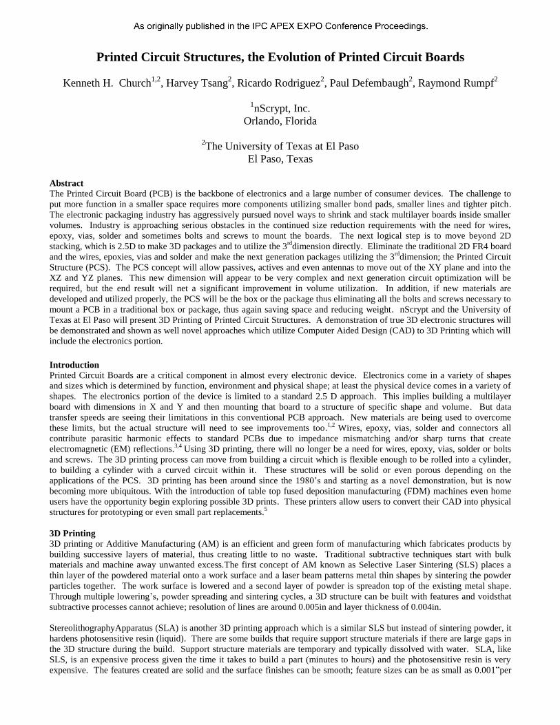
inch for commercial grade tools, but research tools have achieved 0.0001” features. Figure 1 are photos of commercial tools
for 3D printing and Direct Printing.
`
Figure 1 – Commercially available SLA machine on the left and commercially available Direct Print machine on the
right
Fused Deposition Manufacturing (FDM) is another 3D printing approachand uses a heated nozzle to extrude plastic directly
onto a surface. This will print a pattern and then repeat the print thus layering for 3D builds. Like SLA, FDM will
sometimes require a support structure material during builds.The nozzle and head is moved mechanically on a motion
platform and coordinated with the flow of melted plastic flow rate to the XY motion. A disadvantage of FDM is in the
printing process which induces porous structures during the build. This is due to the shape of the extrusion and the fact the
material is not self leveling as this would be counter to the 3D build concept.This process typically requires an 80-90%
overlap of the lines to be placed into the building parameters creating a stable build but also small air pockets. The problem
can be improved with high resolution prints and control of the overlapping parameters. This type of build imposes surface
finishes that are rough and additional post processing is sometimes needed to smooth the surfaces. This approach for 3D
printing has larger features (0.005” at high resolution), but the parts produced are more rigid which allow for functional parts.
Printed Electronics
Printed electronics is a printing process which can pattern an electrical circuit onto various substrates and including cheap
substrates such as vinyl. These processes were designed to be fast, low cost and achieve small features. The screen printing
process is well known for their use in solar cell manufacturing, Low Temperature Cofired Ceramic (LTCC) and multi chip
modules, where screen with a set pattern is laid on top of a substrate and a thick film ink is pressed through the screen. Screen
printing can achieve throughputs of 50 m2/h with a resolution of 100µm.This is standard for manufacturing in industry and
has the ability to produce thick layers from a wide range of high viscosity materials. In addition to using screens there are
Direct Digital Manufacturing (DDM) approaches such as inkjetting. Similar to household printers, inkjets use a low viscosity
ink with solvent materials which are deposited via droplets onto a substrate, line by line. These inkjettable materials can
poses a number of electrical attributes and including being conductive.For many applications, low temperature processing is
required and many of these materials contain additives to enhance adhesion to the surfaceafter low temperature post
processing. Inkjetting can have a throughput of around 100m2/h with a thickness of around 0.0005”.
Electroless plating is another common printing process used extensively in the production of PCBs. This process deposits a
metallic film with the aid of a chemical reducing agent in solution. This allows plating of non-conducting substrates and is
typically used to coat vias after drilling with copper. While electroless plating is typically slower than electrolytic plating,
the resolution is betterand finer and thinner lines can be achieved. This is becoming more attractive as circuits are becoming
smaller and require higher frequency performance, which require higher resolution.
Other forms of printed electronics include the direct print methods (DP), some have coined the phrase Direct Write to
represent these; these include nozzle, quill and aerosol.6
The nozzle method is covered in the 3D Printed Circuit Structures
section below. The quill method deposits material much like a quill pen on paper. The quill tip is dipped into a container of
material which adheres to the tip and then the tip is moved onto a substrate where the material is transferred from the tip and
onto the substrate with 3 axis movement.This method is able to produce 14nm line widths with 5nm spatial resolution, but
only able to build small length scales and requires flat surfaces and custom inks.Inkjet printing has been covered before and
the advantages include high speed printing due to parallelization of print heads, but these approaches typically require flat
surfaces and custom inks that have low viscosities. Just like the inkjet method, aerosol printing requires custom inks that can
be aerosolized, but aerosol has the widest range of working distances and line widths. Aerosol requires the material to be
atomized into a mist which is surrounded by a coaxial sheath of air flowing out of an orifice directed at the substrate;
dimensions as small as 5µm have been done using this approach.Since these are all forms of 3D printing, it is natural to
combine some or all of these methods to create a complete electronic product with small feature sizes and fine conductive
line widths. The possibilities for enhanced performing circuitry will grow whenthe boundaries imposed by a 2D plane are
removed.
Printed Circuit Structures
A PCS is a new area for 3D printing. While early demonstrations were done in the early 2000’s, recent studies and
demonstrations are being presented as a viable alternative to traditional circuit board manufacturing.Unlike conventional
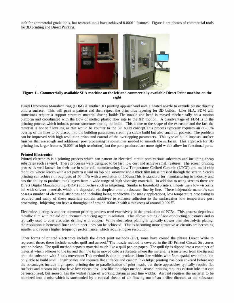
PCBs that build 2D layers consecutively on top of each other (otherwise known as 2.5D). A truly 3D PCS would utilize side
walls, curves and reduce unused volumes that exist in current electronic devices. A graphic artist’s rendition of a true PCS is
shown in figure 2 below.
Figure 2 – A graphic rendition of future PCS
The idea of utilizing the structure as the circuit carrier implies there will be no need for PCB’s. This reaches beyond simple
conformally printing circuits, this approach changes the structure to an electrically functional structure; the electronics are the
structure. In 2D, components can only be placed on a level plane while in 3D components and traces can be built up, around
and within structures. Components can be smoothly integrated into a structure and even hidden within a solid structure
which makes reverse engineering much more challenging. It will also enhance the ruggedness of the device as the device
will become a monolithic piece with no glue, snaps, solder, wiring or bolts. This monolithic piece could also be water proof
as the electrically workings could be buried within the structure leaving no entry point for liquid.The shapes of the structures
will not restrict the printability of electronic components and traces therefore enhanced performing devices may be possible
to include higher gain antennas. Additionally this will be most the most volumetrically optimized approach to electronic
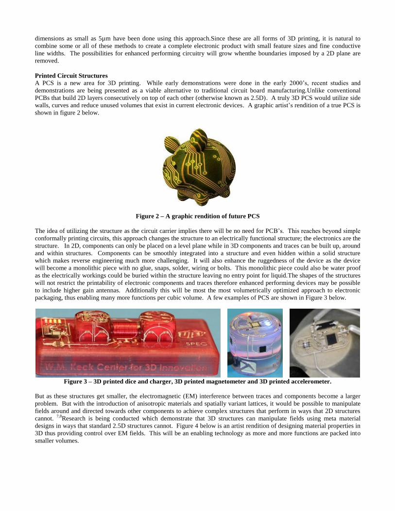
packaging, thus enabling many more functions per cubic volume. A few examples of PCS are shown in Figure 3 below.
Figure 3 – 3D printed dice and charger, 3D printed magnetometer and 3D printed accelerometer.
But as these structures get smaller, the electromagnetic (EM) interference between traces and components become a larger
problem. But with the introduction of anisotropic materials and spatially variant lattices, it would be possible to manipulate
fields around and directed towards other components to achieve complex structures that perform in ways that 2D structures
cannot. 7,8
Research is being conducted which demonstrate that 3D structures can manipulate fields using meta material
designs in ways that standard 2.5D structures cannot. Figure 4 below is an artist rendition of designing material properties in
3D thus providing control over EM fields. This will be an enabling technology as more and more functions are packed into
smaller volumes.
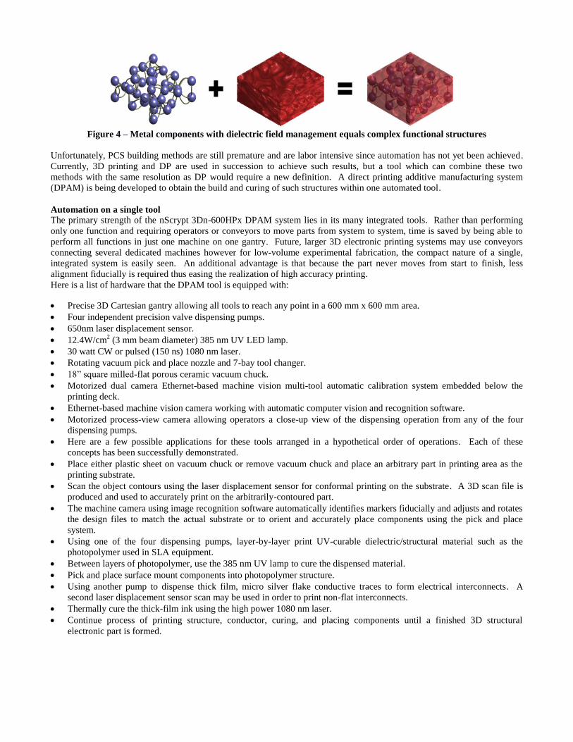
Figure 4 – Metal components with dielectric field management equals complex functional structures
Unfortunately, PCS building methods are still premature and are labor intensive since automation has not yet been achieved.
Currently, 3D printing and DP are used in succession to achieve such results, but a tool which can combine these two
methods with the same resolution as DP would require a new definition. A direct printing additive manufacturing system
(DPAM) is being developed to obtain the build and curing of such structures within one automated tool.
Automation on a single tool
The primary strength of the nScrypt 3Dn-600HPx DPAM system lies in its many integrated tools. Rather than performing
only one function and requiring operators or conveyors to move parts from system to system, time is saved by being able to
perform all functions in just one machine on one gantry. Future, larger 3D electronic printing systems may use conveyors
connecting several dedicated machines however for low-volume experimental fabrication, the compact nature of a single,
integrated system is easily seen. An additional advantage is that because the part never moves from start to finish, less
alignment fiducially is required thus easing the realization of high accuracy printing.
Here is a list of hardware that the DPAM tool is equipped with:
Precise 3D Cartesian gantry allowing all tools to reach any point in a 600 mm x 600 mm area.
Four independent precision valve dispensing pumps.
650nm laser displacement sensor.
12.4W/cm2 (3 mm beam diameter) 385 nm UV LED lamp.
30 watt CW or pulsed (150 ns) 1080 nm laser.
Rotating vacuum pick and place nozzle and 7-bay tool changer.
18” square milled-flat porous ceramic vacuum chuck.
Motorized dual camera Ethernet-based machine vision multi-tool automatic calibration system embedded below the
printing deck.
Ethernet-based machine vision camera working with automatic computer vision and recognition software.
Motorized process-view camera allowing operators a close-up view of the dispensing operation from any of the four
dispensing pumps.
Here are a few possible applications for these tools arranged in a hypothetical order of operations. Each of these
concepts has been successfully demonstrated.
Place either plastic sheet on vacuum chuck or remove vacuum chuck and place an arbitrary part in printing area as the
printing substrate.
Scan the object contours using the laser displacement sensor for conformal printing on the substrate. A 3D scan file is
produced and used to accurately print on the arbitrarily-contoured part.
The machine camera using image recognition software automatically identifies markers fiducially and adjusts and rotates
the design files to match the actual substrate or to orient and accurately place components using the pick and place
system.
Using one of the four dispensing pumps, layer-by-layer print UV-curable dielectric/structural material such as the
photopolymer used in SLA equipment.
Between layers of photopolymer, use the 385 nm UV lamp to cure the dispensed material.
Pick and place surface mount components into photopolymer structure.
Using another pump to dispense thick film, micro silver flake conductive traces to form electrical interconnects. A
second laser displacement sensor scan may be used in order to print non-flat interconnects.
Thermally cure the thick-film ink using the high power 1080 nm laser.
Continue process of printing structure, conductor, curing, and placing components until a finished 3D structural
electronic part is formed.
Process Integration, Synchronization, and Control Hardware
Each of the integrated tool technologies is centrally-controlled by the precise motion control platform. The motion control
platform is connected via IEEE 1394 Serial Bus to the PC. The motion control platform uses multi-axis synchronous motion
in order to print along arbitrary 3D paths as is needed in the case of following the contours measured by the laser
displacement sensor. From the same control system are many digital, analog, and serial inputs and outputs connected to each
of the subsystems such as the UV light, pick and place, etc. In this manner, complete integration of machine operations is
easily achieved because the hardware operations of each device are directly controlled from the central motion control
platform. Each device does, however, have some type of interface electronics so that the complexities of each device’s
control are masked from the central motion control platform. In the case of the laser, for instance, an RS-232 serial port and
a set digital IO lines is used to set the optical power and operation mode of the laser. Each of these signals is adapted by
electronics within the laser control box to control the actual laser diode. In the case of the pick and place system, digital
output modules convert 5V signals from the motion control platform to control pneumatic solenoids for pick and place
vacuum, up/down actuation, and tool changer operation. Each of the tools is controlled in a similar manner.
Software
From a software perspective, designs start as 2D layer drawings in the DXF file format such as slice files generated from 3D
model files in STL format. Each of these layers is called a job and are arranged as a in an ordered list of separate tasks called
a job tree which the machine executes when the ‘run’ button is clicked. Each job has particular attributes such as which tool
is to be used (pump, UV light, laser, etc.) as well as more advanced settings such as 3D laser displacement sensor scan data in
order to print conformal to the actual measured surface. Within each job, a text-based script file is provided which contains
the motion commands as well as custom commands such as “light on/off” or “pick/place” which control each specialized
tool.
In order to achieve smooth, accurate, and perfectly synchronized operations each of the jobs is precompiled into a single
program code file which is first downloaded to the precise motion control hardware from the computer running a real time
kernel (RTX) via IEE 1394 Serial Bus before execution begins. Using this method with the excellent hardware motion
control system allows accuracies of better than 1 micron to be realized.
Operation
From a users’ perspective, the entire system is controlled from a Windows PC running proprietary software. Designers start
with a 3D modeling software then each surface mount component is modeled in 3D and each conductive trace is drawn. The
structure of the part is also modeled around the components and traces. The structural or dielectric components (analogous to
the FR-4 PCB substrate) are sliced and a set of 2D layer files are produced. Conductive areas are also converted to 2D files.
The positions of each component to be pick and placed are measured and saved to a pick and place file. The resulting set of
design files are then imported into the proprietary software as individual jobs and the specifics of each job are assigned such
as whether the given job will be a conductive trace or a layer of structural material. Added to this are jobs which perform 3D
laser displacement scans of the part which will be used to modify the exact printing height of each print job or execute
automated recognition fiducially. Once all the design files have been imported into configured jobs, the set of jobs, called a
project, constitutes a fully-automated 3D printing program code which can be run over and over at the touch of a button.
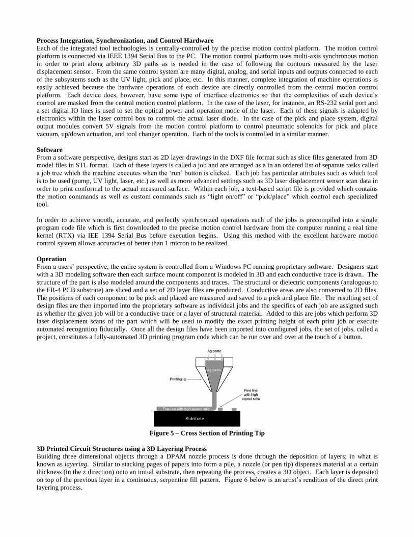
Figure 5 – Cross Section of Printing Tip
3D Printed Circuit Structures using a 3D Layering Process
Building three dimensional objects through a DPAM nozzle process is done through the deposition of layers; in what is
known as layering. Similar to stacking pages of papers into form a pile, a nozzle (or pen tip) dispenses material at a certain
thickness (in the z direction) onto an initial substrate, then repeating the process, creates a 3D object. Each layer is deposited
on top of the previous layer in a continuous, serpentine fill pattern. Figure 6 below is an artist’s rendition of the direct print
layering process.
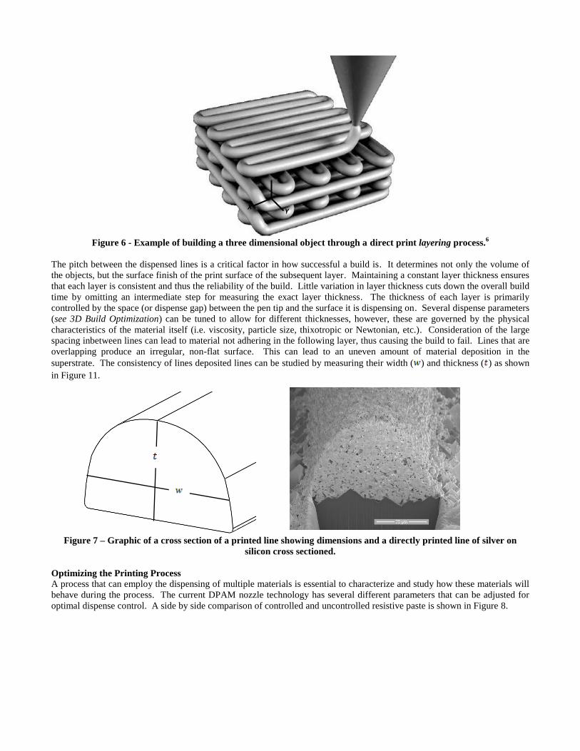
Figure 6 - Example of building a three dimensional object through a direct print layering process.
6
The pitch between the dispensed lines is a critical factor in how successful a build is. It determines not only the volume of
the objects, but the surface finish of the print surface of the subsequent layer. Maintaining a constant layer thickness ensures
that each layer is consistent and thus the reliability of the build. Little variation in layer thickness cuts down the overall build
time by omitting an intermediate step for measuring the exact layer thickness. The thickness of each layer is primarily
controlled by the space (or dispense gap) between the pen tip and the surface it is dispensing on. Several dispense parameters
(see 3D Build Optimization) can be tuned to allow for different thicknesses, however, these are governed by the physical
characteristics of the material itself (i.e. viscosity, particle size, thixotropic or Newtonian, etc.). Consideration of the large
spacing inbetween lines can lead to material not adhering in the following layer, thus causing the build to fail. Lines that are
overlapping produce an irregular, non-flat surface. This can lead to an uneven amount of material deposition in the
superstrate. The consistency of lines deposited lines can be studied by measuring their width ( ) and thickness ( ) as shown
in Figure 11.
Figure 7 – Graphic of a cross section of a printed line showing dimensions and a directly printed line of silver on
silicon cross sectioned.
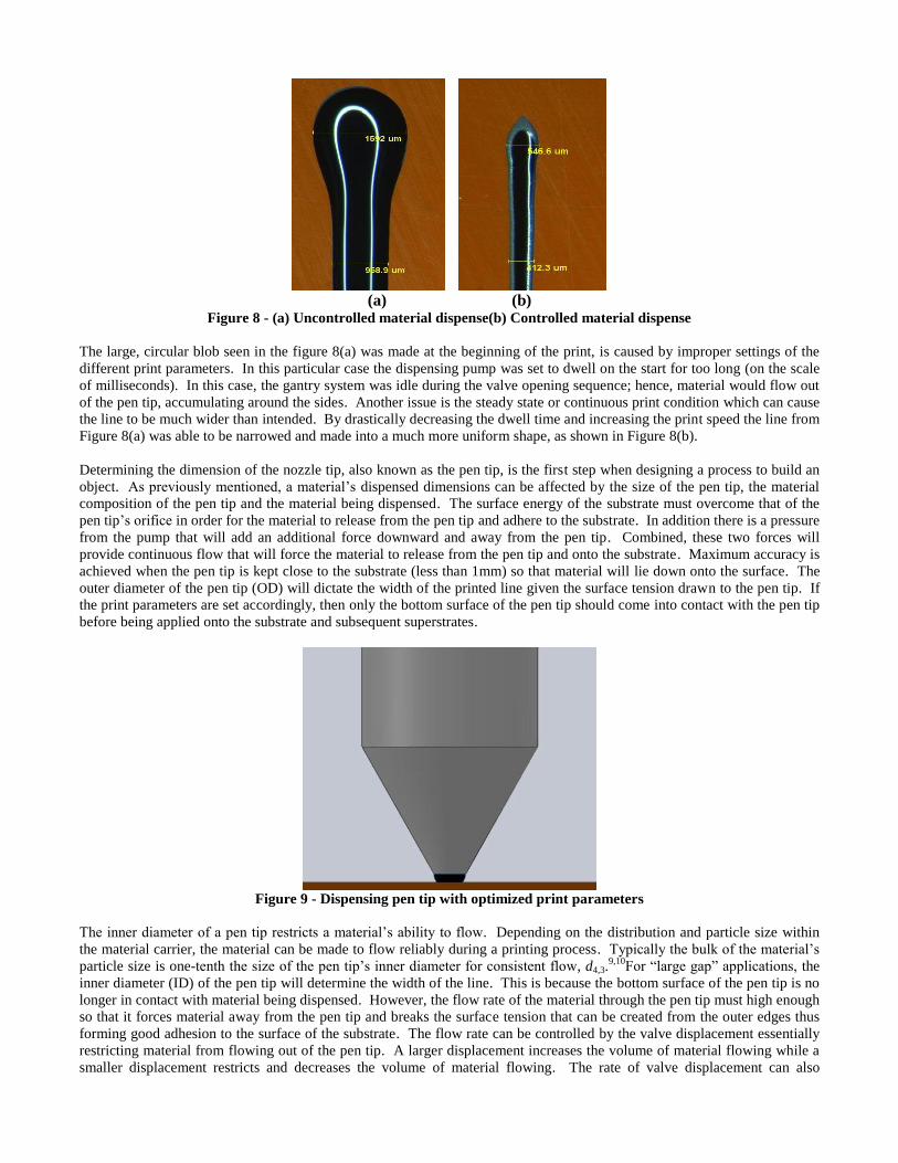
Optimizing the Printing Process
A process that can employ the dispensing of multiple materials is essential to characterize and study how these materials will
behave during the process. The current DPAM nozzle technology has several different parameters that can be adjusted for
optimal dispense control. A side by side comparison of controlled and uncontrolled resistive paste is shown in Figure 8.
X Y
(a) (b)
Figure 8 - (a) Uncontrolled material dispense(b) Controlled material dispense
The large, circular blob seen in the figure 8(a) was made at the beginning of the print, is caused by improper settings of the
different print parameters. In this particular case the dispensing pump was set to dwell on the start for too long (on the scale
of milliseconds). In this case, the gantry system was idle during the valve opening sequence; hence, material would flow out
of the pen tip, accumulating around the sides. Another issue is the steady state or continuous print condition which can cause
the line to be much wider than intended. By drastically decreasing the dwell time and increasing the print speed the line from
Figure 8(a) was able to be narrowed and made into a much more uniform shape, as shown in Figure 8(b).
Determining the dimension of the nozzle tip, also known as the pen tip, is the first step when designing a process to build an
object. As previously mentioned, a material’s dispensed dimensions can be affected by the size of the pen tip, the material
composition of the pen tip and the material being dispensed. The surface energy of the substrate must overcome that of the
pen tip’s orifice in order for the material to release from the pen tip and adhere to the substrate. In addition there is a pressure
from the pump that will add an additional force downward and away from the pen tip. Combined, these two forces will
provide continuous flow that will force the material to release from the pen tip and onto the substrate. Maximum accuracy is
achieved when the pen tip is kept close to the substrate (less than 1mm) so that material will lie down onto the surface. The
outer diameter of the pen tip (OD) will dictate the width of the printed line given the surface tension drawn to the pen tip. If
the print parameters are set accordingly, then only the bottom surface of the pen tip should come into contact with the pen tip
before being applied onto the substrate and subsequent superstrates.
Figure 9 - Dispensing pen tip with optimized print parameters
The inner diameter of a pen tip restricts a material’s ability to flow. Depending on the distribution and particle size within
the material carrier, the material can be made to flow reliably during a printing process. Typically the bulk of the material’s
particle size is one-tenth the size of the pen tip’s inner diameter for consistent flow, d4,3.9,10
For “large gap” applications, the
inner diameter (ID) of the pen tip will determine the width of the line. This is because the bottom surface of the pen tip is no
longer in contact with material being dispensed. However, the flow rate of the material through the pen tip must high enough
so that it forces material away from the pen tip and breaks the surface tension that can be created from the outer edges thus
forming good adhesion to the surface of the substrate. The flow rate can be controlled by the valve displacement essentially
restricting material from flowing out of the pen tip. A larger displacement increases the volume of material flowing while a
smaller displacement restricts and decreases the volume of material flowing. The rate of valve displacement can also
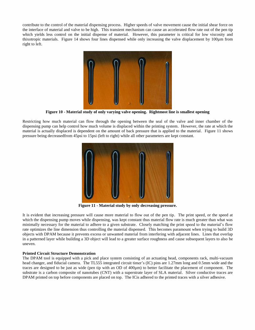
contribute to the control of the material dispensing process. Higher speeds of valve movement cause the initial shear force on
the interface of material and valve to be high. This transient mechanism can cause an accelerated flow rate out of the pen tip
which yields less control on the initial dispense of material. However, this parameter is critical for low viscosity and
thixotropic materials. Figure 14 shows four lines dispensed while only increasing the valve displacement by 100µm from
right to left.
Figure 10 - Material study of only varying valve opening. Rightmost line is smallest opening
Restricting how much material can flow through the opening between the seal of the valve and inner chamber of the
dispensing pump can help control how much volume is displaced within the printing system. However, the rate at which the
material is actually displaced is dependent on the amount of back pressure that is applied to the material. Figure 11 shows
pressure being decreasedfrom 45psi to 15psi (left to right) while all other parameters are kept constant.
Figure 11 - Material study by only decreasing pressure.
It is evident that increasing pressure will cause more material to flow out of the pen tip. The print speed, or the speed at
which the dispensing pump moves while dispensing, was kept constant thus material flow rate is much greater than what was
minimally necessary for the material to adhere to a given substrate. Closely matching the print speed to the material’s flow
rate optimizes the line dimension thus controlling the material dispensed. This becomes paramount when trying to build 3D
objects with DPAM because it prevents excess or unwanted material from interfering with adjacent lines. Lines that overlap
in a patterned layer while building a 3D object will lead to a greater surface roughness and cause subsequent layers to also be
uneven.
Printed Circuit Structure Demonstration
The DPAM tool is equipped with a pick and place system consisting of an actuating head, components rack, multi-vacuum
head changer, and fiducial camera. The TL555 integrated circuit timer’s (IC) pins are 1.27mm long and 0.5mm wide and the
traces are designed to be just as wide (pen tip with an OD of 400µm) to better facilitate the placement of component. The
substrate is a carbon composite of nanotubes (CNT) with a superstrate layer of SLA material. Silver conductive traces are
DPAM printed on top before components are placed on top. The ICis adhered to the printed traces with a silver adhesive.
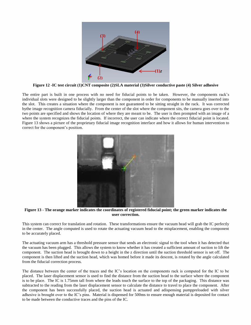
Figure 12 -IC test circuit (1)CNT composite (2)SLA material (3)Silver conductive paste (4) Silver adhesive
The entire part is built in one process with no need for fiducial points to be taken. However, the components rack’s
individual slots were designed to be slightly larger than the component in order for components to be manually inserted into
the slot. This creates a situation where the component is not guaranteed to be sitting straight in the rack. It was corrected
bythe image recognition camera fiducially. From the center of the slot where the component sits, the camera goes over to the
two points are specified and shows the location of where they are meant to be. The user is then prompted with an image of a
where the system recognizes the fiducial points. If incorrect, the user can indicate where the correct fiducial point is located.
Figure 13 shows a picture of the proprietary fiducial image recognition interface and how it allows for human intervention to
correct for the component’s position.
Figure 13 - The orange marker indicates the coordinates of registered fiducial point; the green marker indicates the
user correction.
This system can correct for translation and rotation. These transformations ensure the vacuum head will grab the IC perfectly
in the center. The angle computed is used to rotate the actuating vacuum head to the misplacement, enabling the component
to be accurately placed.
The actuating vacuum arm has a threshold pressure sensor that sends an electronic signal to the tool when it has detected that
the vacuum has been plugged. This allows the system to know whether it has created a sufficient amount of suction to lift the
component. The suction head is brought down to a height in the z direction until the suction threshold sensor is set off. The
component is then lifted and the suction head, which was homed before it made its descent, is rotated by the angle calculated
from the fiducial correction process.
The distance between the center of the traces and the IC’s location on the components rack is computed for the IC to be
placed. The laser displacement sensor is used to find the distance from the suction head to the surface where the component
is to be place. The IC is 1.75mm tall from where the leads touch the surface to the top of the packaging. This distance was
subtracted to the reading from the laser displacement sensor to calculate the distance to travel to place the component. After
the component has been successfully placed, the suction head is actuated and adispensing pumppreloaded with silver
adhesive is brought over to the IC’s pins. Material is dispensed for 500ms to ensure enough material is deposited for contact
to be made between the conductive traces and the pins of the IC.
(1)Z
(3)
(2)
(4)
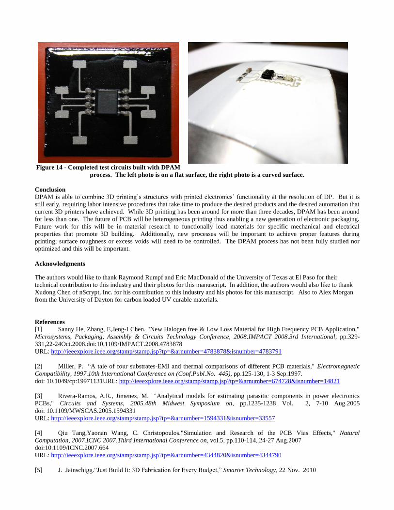
Figure 14 - Completed test circuits built with DPAM
process. The left photo is on a flat surface, the right photo is a curved surface.
Conclusion
DPAM is able to combine 3D printing’s structures with printed electronics’ functionality at the resolution of DP. But it is
still early, requiring labor intensive procedures that take time to produce the desired products and the desired automation that
current 3D printers have achieved. While 3D printing has been around for more than three decades, DPAM has been around
for less than one. The future of PCB will be heterogeneous printing thus enabling a new generation of electronic packaging.
Future work for this will be in material research to functionally load materials for specific mechanical and electrical
properties that promote 3D building. Additionally, new processes will be important to achieve proper features during
printing; surface roughness or excess voids will need to be controlled. The DPAM process has not been fully studied nor
optimized and this will be important.
Acknowledgments
The authors would like to thank Raymond Rumpf and Eric MacDonald of the University of Texas at El Paso for their
technical contribution to this industry and their photos for this manuscript. In addition, the authors would also like to thank
Xudong Chen of nScrypt, Inc. for his contribution to this industry and his photos for this manuscript. Also to Alex Morgan
from the University of Dayton for carbon loaded UV curable materials.
References
[1] Sanny He, Zhang, E,Jeng-I Chen. "New Halogen free & Low Loss Material for High Frequency PCB Application,"
Microsystems, Packaging, Assembly & Circuits Technology Conference, 2008.IMPACT 2008.3rd International, pp.329-
331,22-24Oct.2008.doi:10.1109/IMPACT.2008.4783878
URL: http://ieeexplore.ieee.org/stamp/stamp.jsp?tp=&arnumber=4783878&isnumber=4783791
[2] Miller, P. “A tale of four substrates-EMI and thermal comparisons of different PCB materials," Electromagnetic
Compatibility, 1997.10th International Conference on (Conf.Publ.No. 445), pp.125-130, 1-3 Sep.1997.
doi: 10.1049/cp:19971131URL: http://ieeexplore.ieee.org/stamp/stamp.jsp?tp=&arnumber=674728&isnumber=14821
[3] Rivera-Ramos, A.R., Jimenez, M. "Analytical models for estimating parasitic components in power electronics
PCBs," Circuits and Systems, 2005.48th Midwest Symposium on, pp.1235-1238 Vol. 2, 7-10 Aug.2005
doi: 10.1109/MWSCAS.2005.1594331
URL: http://ieeexplore.ieee.org/stamp/stamp.jsp?tp=&arnumber=1594331&isnumber=33557
[4] Qiu Tang,Yaonan Wang, C. Christopoulos."Simulation and Research of the PCB Vias Effects," Natural
Computation, 2007.ICNC 2007.Third International Conference on, vol.5, pp.110-114, 24-27 Aug.2007
doi:10.1109/ICNC.2007.664
URL: http://ieeexplore.ieee.org/stamp/stamp.jsp?tp=&arnumber=4344820&isnumber=4344790
[5] J. Jainschigg.“Just Build It: 3D Fabrication for Every Budget,” Smarter Technology, 22 Nov. 2010

URL: http://www.smartertechnology.com/index2.php?option=content&do_pdf=1&id=651
[6] Ian Gibson, David Rosen, Brent Stucker. “Additive Manufacturing Technologies: Rapid Prototyping to Direct
Digital Manufacturing”, Springer, New York, Chapter 4, pp 72 – 74
[7] Raymond C. Rumpf, Javier Pazos, Cesar R. Gacia, Luis Ocha and Ryan Wicker.“3D Printed Spatially Variant All-
Dielectric Metamaterials,” Submitted to Phys. Rev.Oct. 2012.
[8] C. R. Garcia, J. Correa, D.Espalin, J. H. Barton, R. C. Rumpf, R. Wicker, and V. Gonzalez, "3D printing of
anisotropic metamaterials," Progress In Electromagnetics Research Letters, Vol. 34, 75-82, 2012.
doi:10.2528/PIERL12070311 http://www.jpier.org/pierl/pier.php?paper=12070311
[9] Diane Burgess, Eric Duffy, Frank Etzler, Anthony Hickey, “Particle Size Analysis: AAPS Workshop Report”, The
AAPS Journal, Vol. 6, No.3, Article 20, September 2004.
[10] ISO 9276-2:2001: Representation of results of particle size analysis – Part 2: Calculation of average particle
sizes/diameters and moments from particle size distributions.