presentazione di powerpoint · • headquarters in catania (director: dr. g. fortunato) •...
TRANSCRIPT
0
Institute for Microelectronics and Microsystems Sede di Roma – Area della ricerca di Roma Tor Vergata – Edificio G
Via del Fosso del Cavaliere 100, 00133 Roma, Italy
http://www.artov.imm.cnr.it/ http://aladin.artov.imm.cnr.it/index.html
http://www.imm.cnr.it/

CNR-Research Area of Tor Vergata
CNR Departments 1. Physical sciences and technologies of matter 2. Earth system science and environmental technology 3. Agrifood science 4. Biomedical sciences 5. Chemical sciences and technology of materials 6. Engineering, ITC and technologies for energy and transport 7. Human and social sciences, cultural heritage
Institute of Translational Pharmacology
Institute of Atmospheric Sciences and Climate
Institute of Acoustic and Sensors "Orso Mario Corbino"
7 In
stitu
tes
National Institute for Astrophysics Institute for Space Astrophysics and Planetology
MICRO/
NANOELETTRONICS
ENERGY
BIOMEDICINE
CLIMATE
ENVIRONMENT
SPACE
TorVergata research area Competences
TorVergata research area

Institute for Microelectronics and Microsystems Department of Physical sciences and technologies of matter
IMM sites in Italy
IMM is organized in six different sites:
• Headquarters in Catania (Director: dr. G. Fortunato)
• Research Units in Lecce, Naples, Rome, Bologna and
Agrate Brianza.
The Institute has a permanent staff of 195 people (117 of them
Researchers) and a temporary staff including 47 post-docs and 61 PhD students
IMM activities span from material science and process development to device
fabrication and system integration, thanks to the micro-nanofabrication facilities
present at the different sites (clean-room areas totaling >1400 m2).
Devices for large-area electronics – Flexible electronics.
High Frequency Microsystems
Tunable Photonic Microsystems
Activity of IMM-Rome
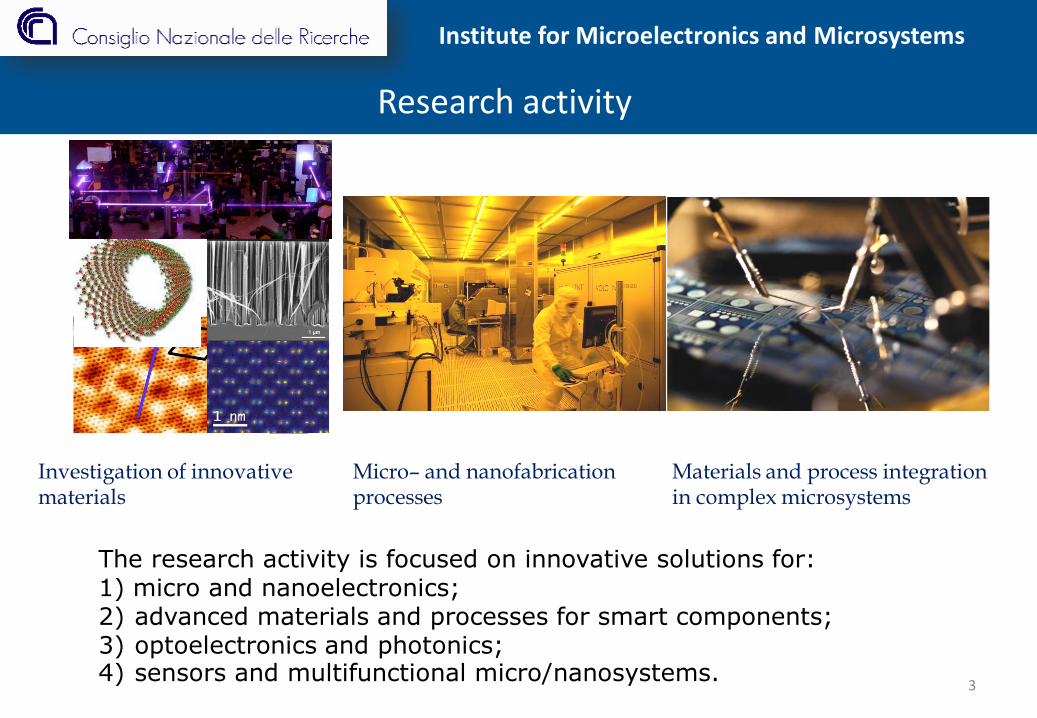
Research activity
3
The research activity is focused on innovative solutions for: 1) micro and nanoelectronics; 2) advanced materials and processes for smart components; 3) optoelectronics and photonics; 4) sensors and multifunctional micro/nanosystems.
Investigation of innovative materials
Micro– and nanofabrication processes
Materials and process integration in complex microsystems
Institute for Microelectronics and Microsystems

Micro/Nano-fabrication facility - equipement
Photolitagraphy
Organic semicondctor evaporator
Ink-jet printer
Gravure printer Screen printer
Co-rotating spin coater
Institute for Microelectronics and Microsystems
Mask aligner
PECVD systems for thin film deposition
Laser annealing Probe stations
FLEX to FLEX interfacing

• Devices for large area electronics based on polycrystalline silicon
Flexible electronics, Smart sensors, Ultra thin microelectrode array, Thin Film Transistors
Flexible Electronics
Institute for Microelectronics and Microsystems
Smart skin for robotics
Biosensors
Microelectrodes on ultra-thin substrates
Gas sensors
3D numerical simulation of physical parameters of a thin film transistor
• Electronics on plastic based on organic and metal oxide semiconductors
Printing of metals and organic semiconductors, Devices electrical characterization, Numerical simulations
• Nanostructured materials for photovoltaic cells and large-area devices
Silicon nanowires, nanotubes, Ultra-sensitive gas sensors
Organic Thin Film Transistors
Strain Gauges:. Bracelet for hand/wrist postures and force estimation, Monitoring of inflatable structures, Safe human-robot interation

Low Temperature Polysilicon (LTPS) TFT technology on polyimide
A. Pecora et al., Solid-State Electronics 52 (2008) 348–352
A. Pecora et al., “Polysilicon thin film transistor circuits for integrated flexible sensors”, Proc. ITC’10, Hyogo (Japan) 2010, p. 298.
Pixel circuit for OLED Display
Touch-Keypad
RFID
inverter
Institute for Microelectronics and Microsystems

Piezoelectric flexible tactile sensor based on poly-silicon TFT for humanoid robots
L.Maiolo et al., Enhanced piezoelectric hybrid tactile sensors fully integrated on ultra-thin polyimide substrates for robotic applications, ICRA 2013, IEEE International Conference on Robotics and Automation
A hand of the humanoid robot iCub
Electronic skin
Institute for Microelectronics and Microsystems
POSFET based on piezoelectric capacitance connected in extended gate configuration with readout circuit based on poly TFTs
Active matix tactile sensors
5x5 sensors
2x2 sensors

Flexible PVDF-TrFE pyroelectric sensor integrated on a fully printed p-channel Organic-TFT
Device scheme
Measurement setup
Sensor response
Common-source amplifier configuration; signal without external amplification
IR laser source l =632 nm laser max. power of 5 mW Chopper frequency up to 500Hz Rbias - Rload in range of MW
Institute for Microelectronics and Microsystems
Monitoring of inflatable structures
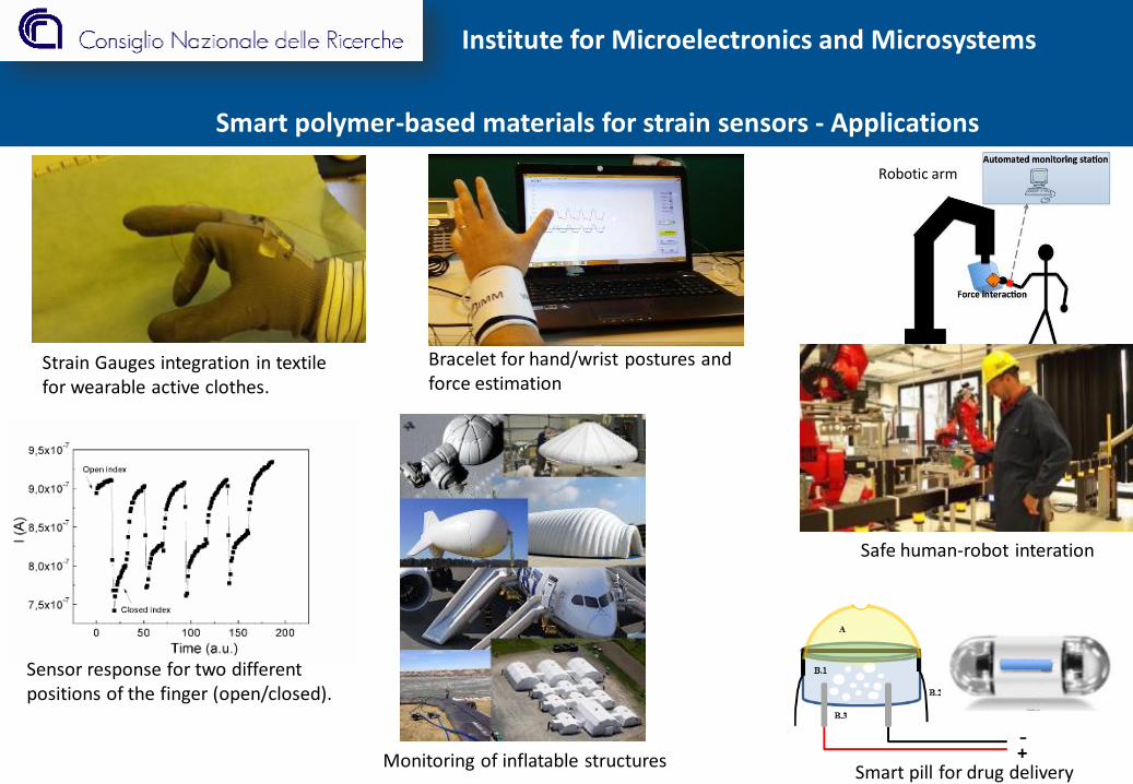
Smart polymer-based materials for strain sensors - Applications
Institute for Microelectronics and Microsystems
Strain Gauges integration in textile for wearable active clothes.
Sensor response for two different positions of the finger (open/closed).
Bracelet for hand/wrist postures and force estimation
Robotic arm
Safe human-robot interation
Applications in Neurological Rehabilitation, sports, measurement of Human Physiological Parameters like the hearthbeat and posture, etc.
Smart pill for drug delivery

Microelectrodes active grid on ultra-flexible substrates (<10 um) for the epicortical brain signal recording
Brain Computer Interface
Institute for Microelectronics and Microsystems
Layout of Ultra Flexible MEAs on polyimide foils.
Active PCB has been equipped with a digital electrophysiology interface chip
Bonding with ACF
ZIF Connector on PCB

5 mm
Resistive sensors Capacitive sensors
Gas sensor systems on flexible substrates with integrated readout electronics
Institute for Microelectronics and Microsystems
Dynamic responses of three
different sensors towards pressure
variations of alcohols
NO2
Working principle
Channel
v v v Bioreceptors
● v v ●
v ● ●
Biomolecules
v v ● ● ●
v
Conductance change
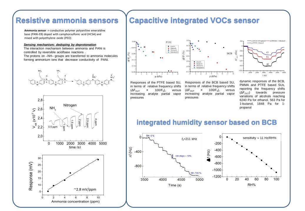
Responses of the PTFE based SU,
in terms of relative frequency shifts
(ΔFOUT × 100/F0), versus
increasing analyte partial vapor
pressures
Responses of the BCB based SU,
in terms of relative frequency shifts
(ΔFOUT × 100/F0), versus
increasing analyte partial vapor
pressures
dynamic responses of the BCB,
PMMA and PTFE based SUs,
reporting the frequency shifts
(ΔFOUT) towards pressure
variations of alcohols reaching
6240 Pa for ethanol, 563 Pa for
1-butanol, 1848 Pa for 1-
propanol
Capacitive integrated VOCs sensor
integrated humidity sensor based on BCB
0 20 40 60 80 100-1200
-1000
-800
-600
-400
-200
0
f (
Hz)
RH%
IDC2 (squares)f0=211 kHz sensitivity 11 Hz/RH%
0 2 4 6 8 10
5
10
15
20
25
30
Re
spo
nse
(m
V)
Ammonia concentration (ppm)
~2.8 mV/ppm
Resistive ammonia sensors
Sensing mechanism: dedoping by deprotonation
The interaction mechanism between ammonia and PANi is
controlled by reversible acid/base reactions .
The protons on –NH– groups are transferred to ammonia molecules
forming ammonium ions that decrease conductivity of PANi.
0 1000 2000 3000 4000 5000
2,0
2,2
2,4
2,6
2,8
4 p
pm
2.5
pp
m
2 p
pm
1.5
pp
m
1 p
pm
Nitrogen
VA
B (
x1
0-2 V
)
time (s)
NH3
0.5 ppm
Ammonia sensor -> conductive polymer polyaniline emeraldine base (PANi-EB) doped with camphorsulfonic acid (HCSA) and mixed with polyethylene oxide (PEO)

M. Cuscunà et al., Low-temperature, self-catalyzed growth of Si nanowires, Nanotechnology 21 (2010)
M. Cuscunà et al., On-chip fabrication of ultrasensitive NO2 sensors based on silicon nanowires, sottomesso su NanoLetters
Si NW based transistors for bio-sensing applications
Schematic of a Si nanowire-based FET device configured as
a sensor with antibody receptors (green), where binding of a
protein with net positive charge (red) yields a decrease in
the conductance
Ultrasensitive NO2 sensors based on silicon nanowires
SiNW trasferiti su strutture interdigitate mediante contact printing
Institute for Microelectronics and Microsystems
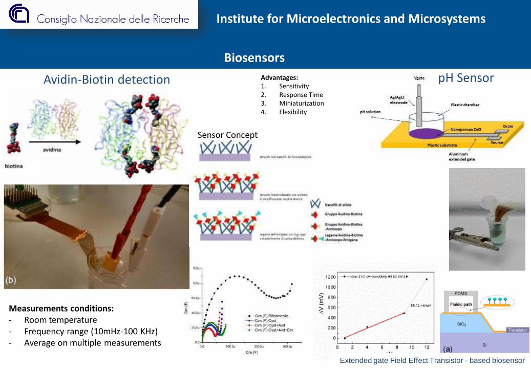
Measurements conditions: - Room temperature - Frequency range (10mHz-100 KHz) - Average on multiple measurements
Sensor Concept
Advantages: 1. Sensitivity 2. Response Time 3. Miniaturization 4. Flexibility
Avidin-Biotin detection
Biosensors
Institute for Microelectronics and Microsystems
Extended gate Field Effect Transistor - based biosensor
pH Sensor

L. Mariucci, CNR-IMM
Organic electronics
3 g/m2
Active matix tactile sensors
Artificial skin
CMOS circuits on flexible plastic substrate
- Low process temperature (<100°C) - Flexible plastic substrates - printable - biocompatibility

Simple and non-conventional sensors
• Organic electrochemical transistors for ion sensing
OECT
G.Tarabella, J.of Mat. Chem.22(2012)23830
OECT on a cotton fiber.
Sweat sensing
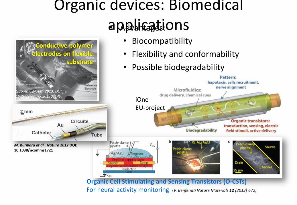
Organic devices: Biomedical applications • Advantages:
• Biocompatibility
• Flexibility and conformability
• Possible biodegradability
Organic Cell Stimulating and Sensing Transistors (O-CSTs) For neural activity monitoring (V. Benfenati Nature Materials 12 (2013) 672)
Conductive polymer electrodes on flexible
substrate
Guo Adv. Mater. 2013, DOI: 10.1002/adma.201304140
iOne EU-project
M. Kuribara et al., Nature 2012 DOI: 10.1038/ncomms1721
OTFT group
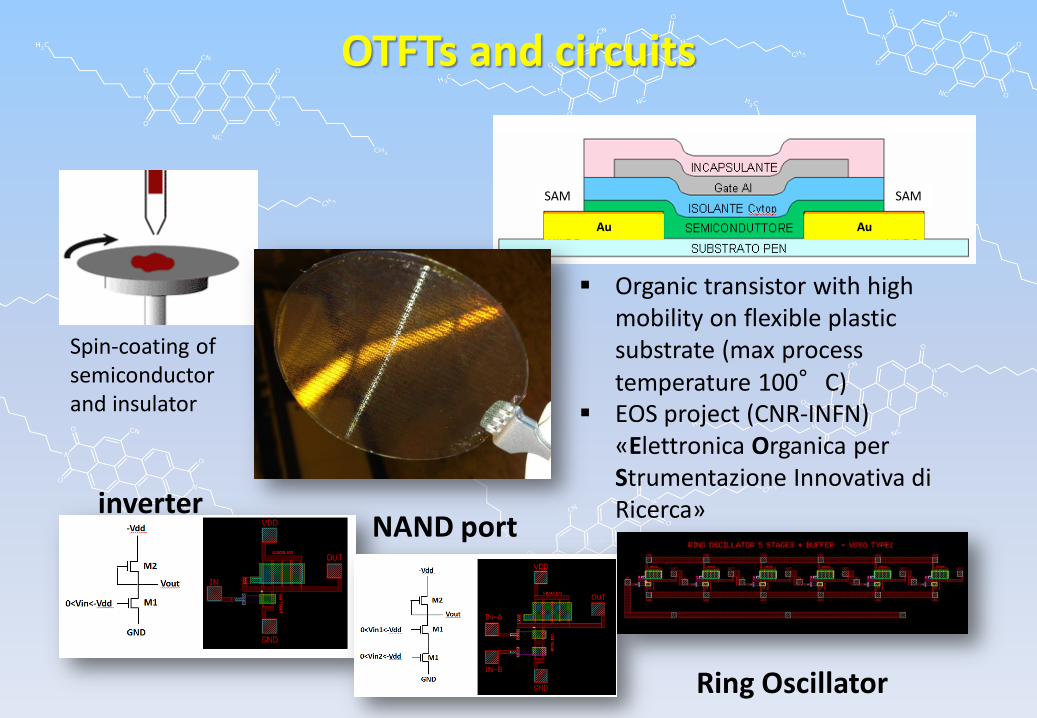
OTFTs and circuits
SAM SAM
Au Au
Organic transistor with high mobility on flexible plastic substrate (max process temperature 100°C)
EOS project (CNR-INFN) «Elettronica Organica per Strumentazione Innovativa di Ricerca» inverter
NAND port
Ring Oscillator
Spin-coating of semiconductor and insulator
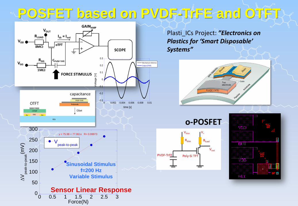
POSFET based on PVDF-TrFE and OTFT
0
50
100
150
200
250
300
0 0.5 1 1.5 2 2.5 3
Sinusoidal Stimulus
f=200 Hz
Variable Stimulus
Sensor Linear Response
Vpeak-to-peak
y = 75.98 + 77.061x R= 0.99973
V
pea
k-t
o-p
ea
k(m
V)
Force(N)
-0.3
-0.2
-0.1
0
0.1
0.2
0.3
0 0.002 0.004 0.006 0.008 0.01
Mechanical reference
Output (PAR)
Vo
ltage
[V
]
time [s]
o-POSFET
Plasti_ICs Project: ”Electronics on Plastics for ‘Smart Disposable’ Systems”
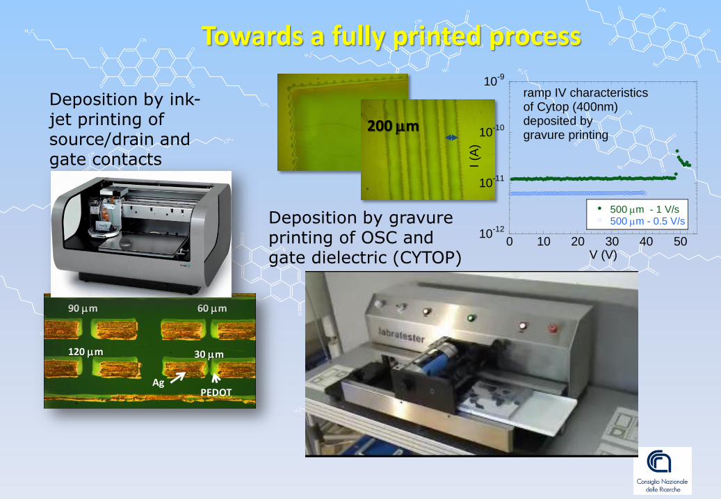
Towards a fully printed process
Deposition by ink-jet printing of source/drain and gate contacts
200 mm
10-12
10-11
10-10
10-9
0 10 20 30 40 50
500 mm - 1 V/s500 mm - 0.5 V/s
I (A
)
V (V)
ramp IV characteristics of Cytop (400nm)deposited by gravure printing
Deposition by gravure printing of OSC and gate dielectric (CYTOP)
PEDOT Ag
120 mm
90 mm 60 mm
30 mm
21
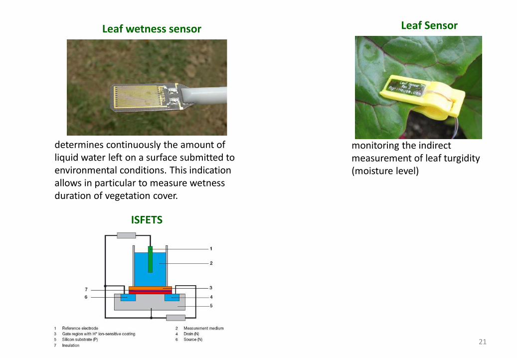
Leaf Sensor
monitoring the indirect measurement of leaf turgidity (moisture level)
Leaf wetness sensor
determines continuously the amount of liquid water left on a surface submitted to environmental conditions. This indication allows in particular to measure wetness duration of vegetation cover.
ISFETS
Sensor functionalization
Istituto per la microelettronica e microsistemi via del Fosso del Cavaliere, 100 - 00133 Roma – ITALIA - http://www.artov.imm.cnr.it/
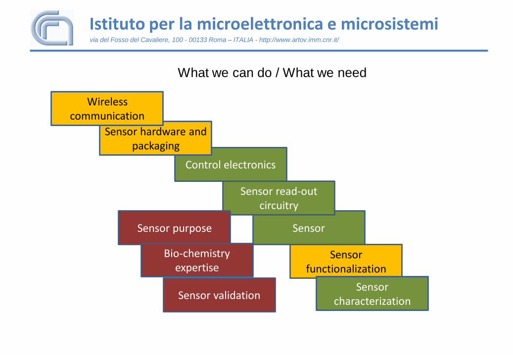
What we can do / What we need
Sensor
Sensor characterization
Sensor read-out circuitry
Control electronics
Sensor hardware and packaging
Wireless communication
Sensor purpose
Sensor validation
Bio-chemistry expertise

other potential applications of Flexible Electronics
Institute for Microelectronics and Microsystems
Flexible RFID
Smart medicine blister
Biosensors Smart packaging: sensors for monitoring of food quality and safety
biosensor platforms
Smart Clothing
Indor gas sensors: VOC, ecc. Outdor gas sensors: NH3, NO2, ecc.
Strain gauge
Sport Automotive Robotics and Reabilitation Electrochemical sensors for food
safety and environmental monitoring

Collaborations with Small Medium Enterprise
Lazio
• Setel Group Srl – Integrated Logistic Support scenario for Defense, Aerospace and Transportation
• Unoauno Srl – Prototipazione rapida 3D
• Systemdesign Srl - Engineering and Manufacturing services, Renewable Energy, Environmental Monitoring Sensors and Systems..
• Geoplanconsulting Srl - Aerofotogrammetria e Termografia aerea
• Fidia Farmaceutici Spa
• Amdl srl – Tecnologie per l’aerospazio
• MITEC Snc - Technological Design RF modules
• Fonderie Digitali srl - Rapid Prototyping
• OA PointGroup srl - Informatica
• Uxi srl - Prodotti web, software, soluzioni ICT
• Keplero srl - Piattaforme software dedicate al monitoraggio dei dati aziendali, Internet of Things.
• Innosensor srl – Sviluppo sensori
• Isolceram srl – Meccanica, innovazioni tecnologiche
• Nanesa srl - Nanomaterials, conductive pastes and hexagonal allotropic compounds
• Augen Srl - Telematica & Automazione
• ST Microelectronics - Semiconduttori
• Space exe srl - high precision wearable GNSS device for sport applications
• OpenPicus Srl - Internet on Things
• Over Technologies – Domotica
• Hs Hospital Service S.P.A. - tecnologie al servizio della medicina
• Aero Sekur Spa - Apparecchiature e sistemi per lì’aerospazio
Lombardia
• BioSAFin Srl – WinSix dispositivi implantari, accessori e tecniche riabilitative
Umbria
• DiaMetra srl - Immunodiagnostic Systems
Toscana
• ARGOS Engineering srl - Progettazione Meccanica, Industriale, Ferroviaria e Green Mobility
• Texe Srl – Textiles & Engineering
• Hospitex Srl - diagnostics instruments
Molise
• Micro BioDevices Srl – In vitro diagnostic medical instrumentation
Polonia
• Tesla - Electronic Manufacturing Services
USA
• VOC instrumentation, LLC - sensor technology
• Absolute process instruments Inc. - Signal Conditioners, Isolators, Process Transmitters Sensors to Solutions
Technological Area of Pordenone www.polo.pn.it; Technological Area of Rome Tiburtina www.tecnopolo.it

Reference contact
Dr. Alessandro Pecora email: [email protected]
Via del Fosso del Cavaliere 100, 00133 Roma, Italy http://www.artov.imm.cnr.it/
http://aladin.artov.imm.cnr.it/index.html
http://www.imm.cnr.it/
Tel: +39 366 8328075
: +39 06 49934064