preparations of tio2 pastes and its application to light-scattering layer for dye-sensitized solar...
TRANSCRIPT
Journal of Industrial and Engineering Chemistry 15 (2009) 724–729
Preparations of TiO2 pastes and its application to light-scattering layerfor dye-sensitized solar cells
Jin-Kook Lee a, Bo-Hwa Jeong a, Sung-il Jang a,b, Young-Guen Kim a,b, Yong-Wook Jang b,Su-Bin Lee a, Mi-Ra Kim a,*a Department of Polymer Science & Engineering, Pusan National University, Busan 609-735, South Koreab POLYCEN Co., Ltd., Busan 608-739, South Korea
A R T I C L E I N F O
Article history:
Received 23 January 2009
Accepted 13 February 2009
Keywords:
Dye-sensitized solar cells
TiO2 paste
Multi-layered TiO2
Light-scattering layer
A B S T R A C T
Three different structures of TiO2 electrodes of the dye-sensitized solar cell (DSSC) devices were
fabricated with layers of nanoparticles and light-scattering particles, and their photovoltaic
performances were investigated when the polymer electrolytes were used. Especially, 20-nm- and
123-nm-TiO2 pastes were prepared by using sol–gel method, to use for light-scattering layer from the
incident light. The best efficiency of 6.03% under AM 1.5 was attained with a multi-layer structure using
123-nm-TiO2 layer for the light-scattering layer and 9-nm-TiO2 layer for the dense layer.
� 2009 The Korean Society of Industrial and Engineering Chemistry. Published by Elsevier B.V. All rights
reserved.
Contents lists available at ScienceDirect
Journal of Industrial and Engineering Chemistry
journal homepage: www.e lsev ier .com/ locate / j iec
1. Introduction
Dye-Sensitized Solar Cells (DSSCs) have attracted considerableinterest as a potential high-efficiency, long-term stable, and lowproduction cost [1–3]. Since Gratzel’s group reported an overallefficiency of DSSC exceeding 11%, many research groups have beenfocused on the improving the photocurrent and photovoltage bydeveloping new dye-sensitizer, suppressing the charge recombi-nation, improving the interfacial interaction and/or modifying theelectrolyte components [4].
Recently, improvement of light harvest efficiency in the dye-adsorbed TiO2 electrode by light scattering has been reported [5–9]. Light-scattering effect can be achieved by additional layers inthe TiO2 layers. Addition of the scattering layers with the largeparticles ensures adequate light trapping in the device [10], due tothe increase of absorption path length of photons and opticalconfinement. Ferber and Luther [6] and Rothenberger et al. [7]confirmed the light-scattering effect with the transport theory andthe many-flux model, respectively. With scattering abilities in theTiO2 films, it is also important that TiO2 electrode has the highersurface area, which is responsible for the optimal dye loading andeffective photocurrent generation.
In this work, multi-layered TiO2 electrodes for DSSCs werefabricated to improve the light harvest efficiency of the dye-
* Corresponding author. Tel.: +82 51 510 3987.
E-mail address: [email protected] (M.-R. Kim).
1226-086X/$ – see front matter � 2009 The Korean Society of Industrial and Engineer
doi:10.1016/j.jiec.2009.09.053
adsorbed TiO2 electrode by light scattering. Three types of TiO2
electrode of the DSSC device were composed of TiO2 particles of9 nm, 20 nm, and 123 nm in the average diameter. Especially, 20-nm- and 123-nm-TiO2 pastes were prepared by using sol–gelmethod, to use for light-scattering layer from the incident light. Inorder to optimize the paste conditions, 20-nm-TiO2 pastes wereprepared as three different kinds of TiO2 pastes on TiO2
concentrations (17 wt.%, 20 wt.% and 24 wt.%). They were intro-duced as the light-scattering layers, and their effect on thephotovoltaic performances of the DSSCs was examined.
2. Experimental details
2.1. Materials
TiO2 powders (P-25, a mixture of Ca. 30% rutile and 70% anatase,BET surface area 50 � 10 m2/g, mean particle size 20 nm) purchasedfrom Degussa AG, Germany. Acetic acid, Triton X-100, acetylacetone,polyethylene glycol (PEG, Mw = 20,000), deionized water, iodine (I2),propylene carbonate (PC), ethylene carbonate (EC), acetonitrile (AN),and tetrabutylammonium iodide (TBAI) were purchased from AldrichCo.
TiO2 paste such as Ti-nanoxide HT/SP (particle size: 9 nm), cis-bis(isothiocyanato)bis(2,20-bipyridyl-4,40-dicarboxylato)-ruthe-nium(II) dye (N3 dye), 1-propyl-3-methylimidazolium iodide(PMII) and 1-hexyl-3-methylimidazolium iodide (HMII) as anionic liquid, F-doped SnO2 glass (SnO2:F glass, 15 V/square) and Ptpaste (Pt catalyst T/SP) were purchased from Solaronix SA.
ing Chemistry. Published by Elsevier B.V. All rights reserved.
Table 1The compositions of 20-nm- and 123-nm-TiO2 pastes.
TiO2 (g) Acetic acid (mL) Triton X (mL) Acetylacetone (mL) PEGc (g) H2Od (mL)
20-nm TiO2 (17 wt.%) 0.60a 0.70 0.70 1.00 0.30 1.40
20-nm TiO2 (20 wt.%) 0.70a 0.70 0.70 1.00 0.30 1.40
20-nm TiO2 (24 wt.%) 0.90a 0.70 0.70 1.00 0.30 1.40
123-nm TiO2 2.40b 0.70 0.70 1.00 0.30 1.40
a P-25 powder.b TiO2 were prepared as Ref. [15].c Polyethylene glycol, Mw = 20,000.d Deionized water.
J.-K. Lee et al. / Journal of Industrial and Engineering Chemistry 15 (2009) 724–729 725
2.2. Preparation of 20-nm- and 123-nm-TiO2 pastes
Three different kinds of 20-nm-TiO2 pastes on TiO2 concentra-tions (17 wt.%, 20 wt.%, and 24 wt.%) were prepared by using sol–gel method and theirs compositions are listed in Table 1.
20-nm-TiO2 paste (24 wt.%) was prepared by addition of1.40 mL of deionized water to 0.90 g of TiO2 powder in an agatemortar. After a 10 min grinding process, an additional 0.30 g of PEGwas added to increase the porosity of the film. After that, 0.70 mL ofacetic acid and 1.00 mL of acetylacetone were added to preventreaggregation of the TiO2 particles and 0.70 mL of Triton X-100 wasintroduced to facilitate the spreading of the colloid on thesubstrate. For the fabrications of 20-nm-TiO2 paste (20 wt.%)and 20-nm-TiO2 paste (17 wt.%), the same procedures werefollowed as described above except using 0.70 g and 0.60 g ofTiO2 powder, respectively.
A 123-nm-TiO2 paste was prepared as the same manner, and itscompositions are also listed in Table 1.
2.3. Fabrications of mono- or multi-layered TiO2 electrodes
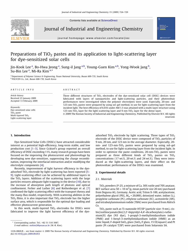
As shown in Fig. 1, three types of the TiO2 electrodes ontoSnO2:F glass were prepared by layer-by-layer deposition of mono-or multi-layered TiO2 pastes by the calcinations at 500 8C. Themulti-layered TiO2 electrode was prepared by repeating squeezingand following calcinations process. Structure (A) composing ofhomogeneous nanoparticle layer, are regarded as a mono-layer,whereas structures (B) and (C) consisting two different layers, areregarded as a multi-layer.
2.4. Fabrications of DSSC devices
We have prepared the DSSC devices, using N3 dye as aphotosensitizer, sandwiched with TiO2 electrode such asmono- or multi-layered TiO2 electrodes and Pt-coatedelectrode as two electrodes. Polymer electrolyte are containingof I2, PMII as an ionic liquid, EC/PC (EC:PC = 4:1, v/v),and polymer matrix such as PEG in acetonitrile. The electrolytewas cast onto the TiO2 electrode adsorbed dyes and was thendried at about 60 8C for 2 h to evaporate wholly the solvent. ThePt-coated electrode was prepared by screen-printing andfollowing calcinations at 400 8C. In assembling of DSSC devices,the TiO2 electrode and the Pt-coated electrode were clampedtogether.
Fig. 1. Three types of TiO2 electrode onto SnO2:F glass prepared for dye-sensitized
solar cells.
2.5. Measurements
The crystal structures of the multi-layered TiO2 films wereanalyzed by X-ray diffraction (XRD) with Cu Ka radiation (X’PertPRO). The nanostructure and surface morphology of the nanos-tructured TiO2 films were characterized by Scanning ElectronMicroscope (SEM). The surface areas and pore sizes of thenanostructured TiO2 films were confirmed by using Brunuaer–Emmett–Teller (BET) and Electrophoretic Light Scattering Spectro-photometer (ELS-8000). Transmittance and absorbance of the filmswere measured by using a UV–vis-NIR spectrophotometer (Varian,Cary 5000). The photovoltaic characteristics of DSSC devices weremeasured by using a Solar Simulator (150 W simulator, PEC-L11/PECCELL) under simulated solar light with ARC Lamp power supply(AM 1.5, 100 mW/cm2). Solar simulator was calibrated to Sireference cell verified. The active area of DSSC device measured byusing a black mask was 0.25 cm2.
3. Results and discussion
3.1. Characterization of the nanostructured 20-nm-TiO2 films
To investigate the influence of TiO2 concentration on thenanostructured TiO2 films, different concentrations of TiO2 powderwere added to a TiO2 paste. P-25 was chosen because of thepossibility to produce crack-free films. Three kinds of TiO2 pastesare listed in Table 1. The nanostructured 20-nm-TiO2 films usingthree kinds of TiO2 pastes on different TiO2 concentrations(17 wt.%, 20 wt.%, and 24 wt.%) were evaluated. Fig. 2 shows theX-ray diffraction-patterns of the nanostructured TiO2 filmscalcinated at 500 8C measured by XRD. The crystal structures ofall the nanostructured TiO2 films exhibited both anatase (1 0 1)
Fig. 2. XRD patterns of three different kinds of 20-nm-TiO2 films (17 wt.%, 20 wt.%
and 24 wt.%) calcinated at 500 8C.

Fig. 3. SEM surface images of three different kinds of 20-nm-TiO2 pastes on TiO2 concentrations of (a) 17 wt.%, (b) 20 wt.%, and (c) 24 wt.% films on the SnO2:F glass after
sintering process.
Table 3
J.-K. Lee et al. / Journal of Industrial and Engineering Chemistry 15 (2009) 724–729726
and rutile (1 1 0) phase. It is observed that the peaks are very sharp,and it shows that when the concentration of TiO2 increases, theamount of rutile changed from anatase also increases. The anataseand rutile, which are two crystalline structures of TiO2 have animportant role on the photovoltaic effects of DSSC devices. Anataseappears as pyramid-like crystals and is formed at low tempera-tures (500–600 8C), where as needle-like rutile crystals aredominantly formed at high temperature processes (>900 8C).The band-gaps of the crystalline forms are 3.2 eV for anatase and3.0 eV for rutile [11]. Anatase has been the main subject of study inDSSCs since it is the primary crystal formed in the usual colloidalpreparation method of the nanocrystalline TiO2 electrode [12].However, recent study revealed that DSSCs with pure rutilestructure exhibited only 30% smaller Jsc than pure anatase andequal Voc [13].
In the SEM surface images of TiO2 films on SnO2:F glasssubstrates of Fig. 3, the small grains with dense structure and wellsurface coverage are observed. The thickness of TiO2 filmscalculated from the cross-section of TiO2 films were about10 mm. The formation of densely and uniformly formed thin filmsprobably could be due to small particle size of TiO2 [14].
BET analysis shows that the three different TiO2 films aftercalcination at a temperature of 500 8C, have a remarkabledifference of surface area. As shown in Table 2, increasing the
Table 2BET and ELS results of sintered three different kinds of 20-nm-TiO2 films on TiO2
concentrations (17 wt.%, 20 wt.%, 24 wt.%) calcinated at 500 8C.
TiO2 Surface
areaa
(m2/g)
Pore
volumea
(m3/g)
Pore
diametera
(nm)
Particle
diameterb
(nm)
20-nm TiO2 (17 wt.%) 61.30 0.09 26.90 222.4
20-nm TiO2 (20 wt.%) 92.00 0.13 25.40 238.4
20-nm TiO2 (24 wt.%) 107.00 0.11 29.30 209.2
a The data were measured by using Brunuaer–Emmett–Teller (BET).b The data were measured by using Electrophoretic Light Scattering Spectro-
photometer (ELS).
concentration of TiO2 in the TiO2 paste increased the total surfacearea from 61.3 m2/g to 107.0 m2/g after the nanostructured TiO2
film was formed, which is predicted that the Jsc value of DSSCdevice will increase. The photocurrent that is produced by theDSSC is linked to the number of dye molecules that are adsorbed onthe surface of the nanostructured TiO2 electrode. Therefore, thehigher the surface area, the higher the photocurrent generated bythe DSSC. However, the numerous cracks in the 20-nm-TiO2
(24 wt.%) film caused by the increase of TiO2 powder concentrationis enough to make the fill factor value fallen. Therefore, thereduction of the fill factor resulted in the decrease of the overallefficiency in DSSC device, although the increase of the photo-current. When a HMII, as an ionic liquid, was introduced in place ofPMII, the Jsc also increased as the increase of surface area in Table 3.
Porosity is another factor that needs to be optimized andimproved the photovoltaic performance on DSSC devices. For thefast regeneration of the oxidized dye and charge transport, theredox electrolyte must be able to penetrate the pores efficientlyand be present in places where the dye penetrates. In general,larger the particle size, the larger will be the porosity of the layer.When the different TiO2 concentration (the particle size is about
Photovoltaic performances of TiO2—17 wt.%, TiO2—20 wt.%, and TiO2—24 wt.%
under light density:100 mW/cm2; AM 1.5, active area: 0.25 cm2.
TiO2 Voc (V) Jsc (mA/cm2) Fill
factor
Efficiency
(%)
20-nm TiO2 (17 wt.%)a 0.73 8.64 0.56 3.53
20-nm TiO2 (20 wt.%)a 0.72 9.73 0.61 4.27
20-nm TiO2 (24 wt.%)a 0.66 10.06 0.58 3.87
20-nm TiO2 (17 wt.%)b 0.72 5.70 0.56 2.30
20-nm TiO2 (20 wt.%)b 0.73 8.34 0.60 3.61
20-nm TiO2 (24 wt.%)b 0.72 8.47 0.57 3.49
a 1-Propyl-3-methylimidazolium iodide (PMII) as an ionic liquid was used in
electrolyte of DSSC device.b 1-Hexyl-3-methylimidazolium iodide (HMII) as an ionic liquid was used in
electrolyte of DSSC device.

Fig. 5. SEM surface images of 123-nm-TiO2 films on the SnO2:F glass after sintering
process.
J.-K. Lee et al. / Journal of Industrial and Engineering Chemistry 15 (2009) 724–729 727
20 nm) is used to prepare the nanostructured TiO2 films, for the 20-nm-TiO2 (20 wt.%) film, the average pore volume increased to0.13 m3/g and the particle diameter distribution was muchbroader, with particle diameters as large as 238.4 nm in Table 2.This pore volume is enough to allow the transport of iodide/tri-iodide ionic species (I�/I3
�) within the pores of the TiO2 films. Onthe other hand, when the pore volume of 20-nm TiO2 of 17 wt.%(0.09 m3/g) is too small to allow the transport of the redox couplecontaining a PEG matrix, there will be an increased probability ofrecombination leading to a decrease in fill factor. The reduction ofthe fill factor caused the decrease of the efficiency and theperformance falling of the devices.
The Jsc, Voc and calculated fill factors and efficiencies measuredunder AM 1.5 illumination are summarized in Table 3. The powerconversion efficiencies of the DSSC devices using the nanostruc-tured TiO2 films as the working electrode and PMII as the ionicliquid showed 3.53–4.27%, and the efficiencies of DSSC devicesusing HMII were 2.30–3.61%.
From the above analysis, we chose the 20-nm-TiO2 paste(20 wt.%), which has the best photovoltaic performances of DSSCdevice, when a multi-layered TiO2 nanostructured films werefabricated.
3.2. Characterization of the 123-nm-TiO2 films
Apart from the 20-nm-TiO2 paste, we have also prepared the123-nm-TiO2 paste, which has larger the nanoparticle, to use alight-scattering layer. Fig. 4 shows the X-ray diffraction-patterns ofthe nanostructured 123-nm-TiO2 films calcinated at 500 8Cmeasured by XRD. The crystal structures of 123-nm-TiO2 filmsexhibited both anatase (1 0 1) and rutile (1 1 0) phase, indicatingthree rutile peaks. 123-nm-TiO2 paste which prepared by usingsol–gel method achieved a high degree of anatase and rutilecrystallinity.
Fig. 5 shows the SEM surface images of 123-nm-TiO2 films onSnO2:F glass substrates after sintering process. 123-nm-TiO2 filmsshowed the small aggregates and relatively well surface coverage.It can be sufficient for the effect of light scattering to be observed inthe double layered TiO2 films.
3.3. Optical properties of the TiO2 films using light-scattering layers
To investigate the absorption effect of the TiO2 films on thelight-scattering layer, the UV–vis absorbance and transmittancespectra of the mono-layered and the multi-layered TiO2 films with
Fig. 4. XRD patterns of 123-nm-TiO2 film calcinated at 500 8C.
a light-scattering layer were measured by using the UV–visspectroscopy. Fig. 6 shows the UV–vis absorbance of the mono-layered TiO2 films (structure (A)) and the multi-layered TiO2 films(structures (B) and (C)) with the scattering layers. Fig. 6(a)illustrates the absorbance spectra of the TiO2 films on the SnO2:F
Fig. 6. Absorbance spectra of the multi-layered TiO2 films of structures (A)–(C). (a)
Absorbance spectra of the TiO2 films on the SnO2:F glass, and (b) absorbance spectra
of N3 dye adsorbed the TiO2 films on the SnO2:F glass.
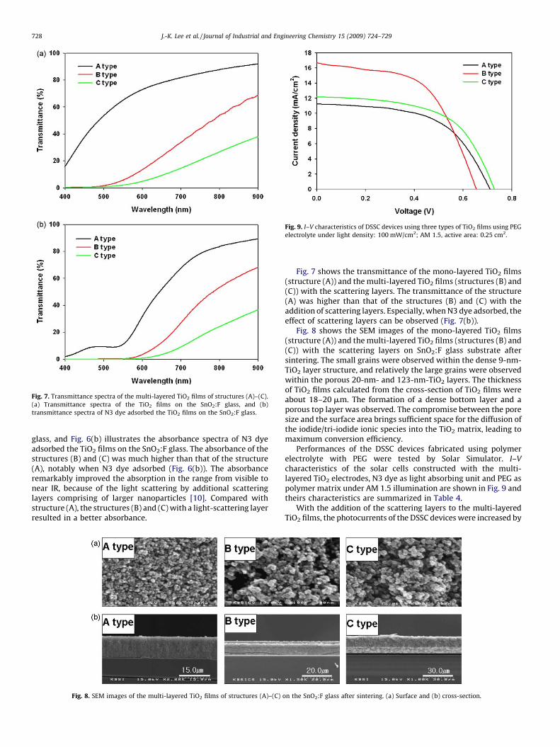
Fig. 7. Transmittance spectra of the multi-layered TiO2 films of structures (A)–(C).
(a) Transmittance spectra of the TiO2 films on the SnO2:F glass, and (b)
transmittance spectra of N3 dye adsorbed the TiO2 films on the SnO2:F glass.
Fig. 9. I–V characteristics of DSSC devices using three types of TiO2 films using PEG
electrolyte under light density: 100 mW/cm2; AM 1.5, active area: 0.25 cm2.
J.-K. Lee et al. / Journal of Industrial and Engineering Chemistry 15 (2009) 724–729728
glass, and Fig. 6(b) illustrates the absorbance spectra of N3 dyeadsorbed the TiO2 films on the SnO2:F glass. The absorbance of thestructures (B) and (C) was much higher than that of the structure(A), notably when N3 dye adsorbed (Fig. 6(b)). The absorbanceremarkably improved the absorption in the range from visible tonear IR, because of the light scattering by additional scatteringlayers comprising of larger nanoparticles [10]. Compared withstructure (A), the structures (B) and (C) with a light-scattering layerresulted in a better absorbance.
Fig. 8. SEM images of the multi-layered TiO2 films of structures (A)–(C) o
Fig. 7 shows the transmittance of the mono-layered TiO2 films(structure (A)) and the multi-layered TiO2 films (structures (B) and(C)) with the scattering layers. The transmittance of the structure(A) was higher than that of the structures (B) and (C) with theaddition of scattering layers. Especially, when N3 dye adsorbed, theeffect of scattering layers can be observed (Fig. 7(b)).
Fig. 8 shows the SEM images of the mono-layered TiO2 films(structure (A)) and the multi-layered TiO2 films (structures (B) and(C)) with the scattering layers on SnO2:F glass substrate aftersintering. The small grains were observed within the dense 9-nm-TiO2 layer structure, and relatively the large grains were observedwithin the porous 20-nm- and 123-nm-TiO2 layers. The thicknessof TiO2 films calculated from the cross-section of TiO2 films wereabout 18–20 mm. The formation of a dense bottom layer and aporous top layer was observed. The compromise between the poresize and the surface area brings sufficient space for the diffusion ofthe iodide/tri-iodide ionic species into the TiO2 matrix, leading tomaximum conversion efficiency.
Performances of the DSSC devices fabricated using polymerelectrolyte with PEG were tested by Solar Simulator. I–V
characteristics of the solar cells constructed with the multi-layered TiO2 electrodes, N3 dye as light absorbing unit and PEG aspolymer matrix under AM 1.5 illumination are shown in Fig. 9 andtheirs characteristics are summarized in Table 4.
With the addition of the scattering layers to the multi-layeredTiO2 films, the photocurrents of the DSSC devices were increased by
n the SnO2:F glass after sintering. (a) Surface and (b) cross-section.

Table 4Photovoltaic performances of DSSC devicesa based three types of TiO2 films using polymer electrolyte under light density: 100 mW/cm2; AM 1.5, active area: 0.25 cm2.
Type of structure TiO2 type Voc (V) Jsc (mA/cm2) Fill factor Efficiency (%)
Dense layer Light-scattering layer
A type 9 nmb – 0.71 11.20 0.56 4.43
B type 9 nmb 123-nm TiO2c 0.65 16.70 0.55 6.03
C type 9 nmb 20-nm TiO2 (20 wt.%)c 0.73 12.19 0.57 5.04
a DSSC devices fabricated by the method in Section 2.4.b TiO2 films prepared by Ti-nanoxide HT/SP (particle size: 9 nm) purchased from Solaronix SA.c TiO2 films prepared by TiO2 pastes with the composition in Table 1 and the method in Section 2.2.
J.-K. Lee et al. / Journal of Industrial and Engineering Chemistry 15 (2009) 724–729 729
nearly 50%, compared to those of the devices without the scatteringlayers. Structure (B) with the 123-nm-TiO2 layer for light-scatteringlayer obtained higher Jsc than structure (C) with the 20-nm-TiO2
layer, however, Voc showed lower value. Due to the improving the Jsc
value, remarkably high power conversion efficiencies of the DSSCdevices were observed, despite the application to the polymerelectrolytes. This result was caused by the scattering properties ofthe TiO2 films which have the light capture inside the device. As aresult, the best power conversion efficiency of 6.03% underillumination of simulated AM 1.5 solar light (100 mW/cm2) wasattained with a multi-layer structure using 123-nm-TiO2 layer forthe light-scattering layer and 9-nm-TiO2 layer for the dense layer.
4. Conclusion
In conclusion, we investigated the improvement of the DSSCperformance afforded by using multi-layered TiO2 electrodes bylight-scattering effect. 9-nm-TiO2 layers were used for the denselayer and 20-nm- or 123-nm-TiO2 layers were used for light-scattering layer from the incident light. The use of the light-scattering layers resulted in an increase of the Jsc value, thus theoverall power conversion efficiency of the DSSC device based onPEG electrolyte was achieved by 6.03% when 123-nm-TiO2 layerswere used as light-scattering layer.
Acknowledgement
This work was supported for two years by Pusan NationalUniversity Research Grant.
References
[1] B.O. Regan, M. Gratzel, Nature 353 (1991) 737.[2] M.K. Nazzeeruddin, A. Kay, I. Rodicio, R. Humphry Baker, E. Miller, P. Liska, N.
Vlachopoulus, M. Gratzel, J. Am. Chem. Soc. 115 (1993) 6382.[3] (A) A. Jagfeldt, M. Gratzel, Chem. Rev. 95 (1995) 49;
(B) H.K. Song, Y.H. Park, C.H. Han, J.G. Jee, J. Ind. Eng. Chem. 15 (2009) 62.[4] F.C. Krebs, M. Biancardo, Sol. Energy Mater. Sol. Cells 90 (2006) 142.[5] A. Usami, Chem. Phys. Lett. 277 (1997) 105.[6] J. Ferber, J. Luther, Sol. Energy Mater. Sol. Cells 54 (1998) 265.[7] G. Rothenberger, P. Comte, M. Gratzel, Sol. Energy Mater. Sol. Cells 58 (1999)
321.[8] A. Usami, Sol. Energy Mater. Sol. Cells 59 (1999) 163.[9] A. Usami, Sol. Energy Mater. Sol. Cells 64 (2000) 73.
[10] S. Hore, C. Vetter, R. Kern, H. Smit, A. Hinsch, Sol. Energy Mater. Sol. Cells 90 (2006)1176.
[11] K. Kalyanasundaram, M. Gratzel, Coord. Chem. Rev. 177 (1998) 347.[12] C.J. Barbe, F. Arendse, P. Comte, M. Jirousek, F. Lenzmann, V. Shklover, M. Gratzel, J.
Am. Ceram. Soc. 80 (12) (1997) 3157.[13] N.G. Park, J. Van de Labemaat, A.J. Frank, J. Phys. Chem. B 104 (2000) 8989.[14] C.-Y. Huang, Y.-C. Hsu, J.-G. Chen, V. Suryanarayanan, K.-M. Lee, K.-C. Ho, Sol.
Energy Mater. Sol. Cell 90 (15) (2006) 2391.[15] S. Mahshid, M. Askari, M. Sasani Ghamsari, J. Mater. Process. Technol. 189 (2007)
296.