practical optimization flow using a new system design
TRANSCRIPT

118
Transactions of The Japan Institute of Electronics Packaging Vol. 8, No. 1, 2015
1. IntroductionIn recent years, improving the speed and performance
of CMOS devices which serve as the basic component in
current semiconductor devices has been realized through
hyper-miniaturization technologies. The miniaturization
technologies have extended beyond the 1x nm node. How-
ever, to further increase speed and performance, the sig-
nal delay in global wiring used for connection of individual
IPs within a chip will be a crucial issue. As a means of sat-
isfying various requirements such as shortening the wir-
ing length, wafer-level three-dimensional integrated cir-
cuits (3DICs) have been proposed.[1] On the other hand,
due to the inclusion of many different types of elements,
product systems using 2D or 3D ICs are large scale and
complex which, in turn, makes system design very diffi-
cult. So far, we have constructed the system design meth-
odology for 3DICs, and proposed a practical method for
the design of large scale and complex systems.
In practice, design optimization is complicated and time-
consuming. To resolve this issue, the System Design Sys-
tem Integration-Cubic (SDSI-Cubic) has been proposed
(Fig. 1).[2] This methodology is applicable for the entire
product system. It efficiently and automatically optimizes
the system by combining various systems engineering
methods based on a defined system profile. However, the
previous design example using the SDSI-Cubic itself was
in early development and it had not been applied to an
practical product design.[3]
In this paper, we apply the SDSI-Cubic to optimize the
design of a radiation measurement system. Thus far, we
have developed technologies for different elements or
components of the radiation measurement system and
made a prototype.[4] However, the prototype does not sat-
isfy all requirements due to priority being placed on sensor
design rather than the entire system, and because the
design was based on human experience and intuition.
The radiation measurement system is an embedded sys-
tem, which requires a small, light weight form factor and
high cost-performance. For dealing with the March 2011
Fukushima nuclear disaster in Japan, residents in
Fukushima disaster area are in immediate need of an eas-
ily available measurement system to measure radiation
and radioactivity. This is the background of the system we
consider in this paper. To satisfy all these design require-
ments, it is necessary to resolve conflicting requirements
within the system and create an optimal design. In addition
to the sensor design, the implementation of various func-
tionalities such as waveform processing and calculation is
designed by first properly assigning it to hardware (Ana-
log Circuits and FPGA) or software for CPU. Moreover, we
[Technical Paper]
Practical Optimization Flow using a New System Design
MethodologyKen Kawamura*, Hidenori Murata*, Yoshiharu Iwata*, Ryohei Satoh**, and Kazuya Okamoto**
*Graduate School of Engineering, Osaka University, 2-1 Yamadaoka, Suita, Osaka 565-0871, Japan
**Osaka University Office for University-Industry Collaboration, 2-1 Yamadaoka, Suita, Osaka 565-0871, Japan
(Received July 31, 2015; accepted November 19, 2015)
Abstract
An efficient design flow for a radiation measurement system using the SDSI-Cubic (System Design System Integration-
Cubic) is demonstrated. The system itself is embedded and, therefore, requires a small-form factor and high cost-perfor-
mance amongst other things. In addition to sensor design, the implementation of various functionalities such as waveform
processing and calculation is designed by proper assignment/implementation to hardware (analog circuits and FPGA) or
software for the CPU. Moreover, the entire system optimized while accounting for the conflicting requirements of mul-
tiple subsystem designs. By optimizing the system configuration, a high cost-performance portable radiation dose and
radioactivity measurement system is developed.
Keywords: IC Design, System Design, SDSI-Cubic, SysML, Measurement System
Copyright © The Japan Institute of Electronics Packaging

119
Kawamura et al.: Practical Optimization Flow using a New System Design Methodology (2/9)
optimize the entire system considering various system
structure proposals and conflicting design issues.
2. Outline of SDSI-CubicThe SDSI-Cubic method is a system design framework
for the design optimization of large-scale and complex sys-
tem. As shown in Fig. 1, this framework performs auto-
matic optimization using an algorithm which classifies the
systems engineering technology into 6 faces.[5] These
faces correspond to each stage of the system design flow.
Face-1 is the “Input.” It is where input of product system
information and a design intention is performed. Face-2 is
the description and analysis of product information. It is
where system profile definition is performed. Face-3 is the
execution and processing of product information. It is
where the relation between each design problem of a prod-
uct system is formulated, and it changes into the state
which can be evaluated. Face-4 is the description and anal-
ysis of process information. It is where efficient design
process is constructed. Face-5 is execution and processing
of process information. It is where the optimal design solu-
tion is derived. Face-6 is the “output.” It is where the out-
put of a result is performed. This method optimizes the
system design automatically based on the information of
the system profile definition (Face-2). Therefore, the sys-
tem profile definition is very important.
Next, we describe the Face-2 system profile definition
method. The purpose of Face 2 is to process the product
system on a computer by defining and describing paramet-
ric models, and to extract design tasks to perform execu-
tion and processing in Faces-3 and -4.
We use the Systems Modeling Language (SysML) to
create a system profile definition. SysML is a modeling
language developed to support specification, analysis,
design, confirmation, and verification of the whole system
which includes hardware, software, data, procedure, and
equipment. In addition, SysML provides a semantic and
diagrammatic base to represent models for requirements,
behavior, structure, and integration of system reflecting an
engineering result. The diagram of SysML is shown in Fig.
2. A system is described using 9 diagrams ({a}-{i} in Fig. 2)
each belonging to one of 3 different types, i.e., require-
ment, behavior, or structure.[6] In addition, Fig. 2 also
shows an optimization diagram ({j}) and allocation dia-
gram ({k}) which were added to enable optimization using
the SDSI-Cubic.
The SDSI-Cubic system profile definition uses 4 dia-
grams of SysML to describe the system model to be opti-
Fig. 1 SDSI-Cubic Framework.
Fig. 2 The broad view of SysML.

120
Transactions of The Japan Institute of Electronics Packaging Vol. 8, No. 1, 2015
mized (Fig. 3). Four diagrams are a block diagram, an
internal block diagram, a parametric diagram, and newly
added optimization diagram. By using these diagrams,
information about the optimization problem can be
described. In a system profile, information of the system
structure is described in the block diagram (Fig. 3 (a)),
information of the attributes are described in the internal
block diagram (Fig. 3 (b)), information of the constraints
between the attributes are described in the parametric dia-
gram (Fig. 3 (c)). Moreover, Fig. 3 (d) shows the objective
function and the design parameters of optimization are
expressed in the optimization diagram. In addition, an allo-
cation diagram is prepared to describe and evaluate the
choice of system structures such as selection of hardware
or software.[7]
3. System Profile Definition of Radiation Measure-ment System
In this research, we design a radiation measurement
system using a scintillation counter based on information
obtained from the preceding section. The scintillation
counter uses a scintillator crystal for the sensor. Moreover,
we represent the system using the structures as shown in
Fig. 4. The system consists of a sensor, a processing cir-
cuit, a display, a Pb radiation shield, a sample container, a
case and so forth, with various functionalities, such as
gamma rays acquisition, signal processing, calculation,
and result output. Design proposal 1 focuses a balance of
sensitivity, detection limit, and price. Design proposal 2
considers detecting radiation from sample more efficiently
by using 2 sensors. Design proposal 3 focuses on detecting
radiation from sample more efficiently by enclosing the
sensor with the sample.
Next, we define the radiation measurement system
requirements as well as consider design conflicts. Resi-Fig. 3 SysML diagrams for SDSI-Cubic.
(a) Block diagram.
(b) Internal block diagram.
(c) Parametric diagram.
(d) Optimization diagram.
Fig. 4 Design proposal of the radiation measurement system.

121
Kawamura et al.: Practical Optimization Flow using a New System Design Methodology (4/9)
dents in the Fukushima disaster area require a high cost-
performance system which can check the safety of radia-
tion easily. In particular, we require high sensitivity (1,300
cpm/(μSv/h) or more), high resolution (10% or less), low
detection limit (50 Bq/kg or less), light weight (10 kg or
less), small size (5,000 cm3 or less), and low price (about
1/3 price of existing system). For example, the electrical
circuit requirement is high speed for high sensitivity, and
low noise for high resolution and low detection limit. How-
ever, it conflicts with the requirement of low price since a
high-performance circuit is expensive. Therefore, we need
an optimum design which resolves these conflicts.
In addition to the sensor design, an important aspect of
this design is the assignment of γ -ray signal acquisition,
processing and calculation functionalities to hardware
(analog circuit, FPGA) or software (CPU). We use an allo-
cation diagram to represent the case when there are multi-
ple approach options to realize functionality (Fig. 5). We
define the program size from the processing algorithm
and we formulate choice, cost, functionality and others for
each component. By putting attributes (parameters) in
internal blocks, we represent constraints using parametric
diagrams.
We must answer the following questions regarding how
to implement/assign functionalities:
1) Should the pulse height analysis functionality
(which detects peak voltage from the conversion
voltage of a gamma ray signal) be implemented
using a FPGA or CPU (Fig. 5 (a))?
2) Should the functionality of the spectrum creation
functionality which changes and integrates a pulse
height to an energy value be implemented using a
FPGA or CPU (Fig. 5 (b))?
3) Should the calculations used for radioactivity and
radiation dose measurement functionality be imple-
mented in CPU, notebook PC or tablet PC (Fig. 5
(c))?
4) Should the user interface functionality, e.g., input
and result output, be implemented in a notebook
PC, tablet PC, or a dedicated board including CPU,
button, and display (Fig. 5 (d))?
In addition, we note our system structure will change
dramatically according to our hardware selection. There-
fore, we classify our parametric model into two types of
information which we represent using a parametric dia-
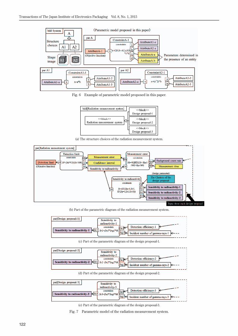
gram (Fig. 6). The first type is the shape-independent
information while the second consists of all other informa-
tion. The shape-independent information consists of all
parameters and constraints which are determined by exis-
tence of an entity. An example of a parametric model of the
radiation measurement system is shown in Fig. 7. The
design proposal choices are described using an allocation
diagram (Fig. 7 (a)). The constraints which are indepen-
dent of the design proposals are described in a parametric
diagram of the radiation measurement system (Fig. 7 (b)).
The constraints which depend on the design proposals are
described in a parametric diagram of each design proposal
(Fig. 7 (c), (d), and (e)). By isolating the shape-indepen-
dent information we make it easy to change a shape pro-
posal and modify the model.
In this design, we define an evaluation value function
shown in (1) which we optimize by maximizing its value.
Moreover, we define the following design parameters, i.e.,
design proposal choices, functionality assignment choices,
Fig. 5 The structure choices of each functionality.
(a) The pulse height analysis functionality. (b) The spectrum creation functionality.
(c) The radioactivity and radiation dose measurement functionality.
(d) The user interface functionality.
122
Transactions of The Japan Institute of Electronics Packaging Vol. 8, No. 1, 2015
Fig. 6 Example of parametric model proposed in this paper.
Fig. 7 Parametric model of the radiation measurement system.
(a) The structure choices of the radiation measurement system.
(b) Part of the parametric diagram of the radiation measurement system.
(c) Part of the parametric diagram of the design proposal-1.
(d) Part of the parametric diagram of the design proposal-2.
(e) Part of the parametric diagram of the design proposal-3.

123
Kawamura et al.: Practical Optimization Flow using a New System Design Methodology (6/9)
sensor crystal size, Pb shield thickness, and capacity of
sample container. The comparison of the evaluation value
(SDSI-C) for each design parameter is shown in Table 1.
The design proposal choices are related to sensitivity,
detection limit, weight, volume, and price. The functional-
ity assignment choices are related to price. The sensor
crystal size is related to sensitivity, resolution, detection
limit, and price. The Pb shield thickness is related to detec-
tion limit, weight, and volume. The Sample container
capacity is related to detection limit, weight, and volume.
We represent these design parameters in an optimization
diagram.
SDSI-C = S /( R · L · P · W · V ) (1)
Here, SDSI-C: Evaluation value, S: Sensitivity, R: Resolu-
tion, L: Detection limit, P: Price, W: Weight, and V: Volume.
We define the system structure, the attribute (parame-
ter) of each block, and the formulated constraints of the
relation between each attribute. We then create a system
profile by representing the system structure, the attribute
(parameter) of each block, and the formulated constraints
using the block diagram, internal block diagram, and para-
metric diagram, respectively.
4. Results and DiscussionWe use the Face-2 system profile definition discussed in
section III, and optimize the radiation measurement sys-
tem using the SDSI-Cubic. 26 design tasks shown in Fig. 8
(design Task1-26) are extracted in Face-2, i.e., design task
1: Input of the initial values; design tasks 2–10: Data acqui-
sition from database of each part (the amplifier circuit, the
photodetector, the calculation part, the position sensor, the
spectrum creation part, the user interface part, the com-
munication part, the peak value detector, and the power
supply part); design tasks 11–19: Calculating cost of each
part (the user interface part, the position sensor, the spec-
trum creation part, the peak value detector, the calculation
part, the communication part, the power supply part, the
amplifier circuit, and the photodetector); design task 20:
Calculating the gamma rays emitted by the sample; design
task 21: Calculating weight of the Pb shield and shielding
effect; design task 22: Calculating the gamma rays emitted
by a standard radiation source; design task 23: Calculating
sensitivity and detection efficiency; design task 24: Calcu-
lating detection limit; design task 25: Calculating total cost
(price), total volume and total weight; design task 26: Cal-
culating resolution. We add design tasks of design parame-
ters (design Task00-010) to change the design parameters
in optimization. The generated task group consists of 37
design tasks (design Task1-26 and design Task00-010). We
use the DSM (Design Structure Matrix[8]) to construct a
design procedure for this task group using a minimal
amount of rework (Fig. 8). In Fig. 8, 6 optimization prob-
lems are defined and each line expresses a design task.
OPT1 is an optimization problem of minimizing cost of the
user interface. The design parameter is the user interface
choices (notebook PC, tablet PC, or a dedicated board).
OPT2 is an optimization problem of minimizing cost of the
calculation part. The design parameter is the hardware
choice needed to perform the calculation (CPU, notebook
PC, or tablet PC). OPT3 is an optimization problem of min-
imizing cost of the peak value detector. The design param-
eter is the choice of peak value detector (FPGA or CPU).
OPT4 is an optimization problem of minimizing cost of the
spectrum creation part. The design parameter is the
choice of spectrum creation functionality hardware (FPGA
Table 1 Comparison of the evaluation value (SDSI-C) for each design parameter.
Evaluation value Objective function Design parameter
No.SDSI-C Sensitivity Resolution Detection
limit Weight Volume Price Design proposal
Pulse height
analysis
Spectrum creation Calculation User
interface
Sensor crystal
size
Pb shield thickness
Sample container capacity
(×10-11) (×104)cpm % Bq/kg kg cm3 (104)yen cm3 mm cm3
1 1.31 2.5 9 52 10 4,500 16 1
CPU CPU Tablet PC Tablet PC 25 10 4502 1.60↑ 4.3 9 47 11 5,500 20 2
3 0.26↓ 2.5 9 38 20 12,000 17 3
1 1.31 2.5 9 52 10 4,500 16
1
CPU CPU Tablet PC Tablet PC
25 10 4504 1.30↓ 2.5 9 52 10 4,500 16.1 FPGA FPGA Tablet PC Tablet PC
5 1.27↓ 2.5 9 52 10 4,500 16.4 CPU CPU CPU Tablet PC
1 1.31 2.5 9 52 10 4,500 16
1 CPU CPU Tablet PC Tablet PC
25 10 450
6 0.37↓ 0.9 9.5 64 10 4,500 14 9 10 450
7 1.54↑ 2.5 9 64 8 4,200 16 25 5 450
8 1.54↑ 2.5 9 78 8 3,500 16 25 10 230

124
Transactions of The Japan Institute of Electronics Packaging Vol. 8, No. 1, 2015
or CPU). OPT5 is an optimization problem of maximizing
sensitivity, shielding effect and detection efficiency, and
minimizing Pb shield weight and each part cost. The
design parameters are the sensor crystal size, Pb shield
thickness, sample container capacity, and the design pro-
posal choices (design proposal 1, 2, or 3). OPT6 is an opti-
mization problem of minimizing detection limit. The
design parameter is the measurement time. In this study,
the measurement time is 30 minutes. An optimization
result of the radiation measurement system is derived by
performing in order optimization (OPT1-4), calculation
(design Task10/2/22/3/5/8), optimization (OPT5), calcu-
lation (design Task11-19), optimization (OPT6), and calcu-
lation (design Task25/26).
The optimization results are shown in Fig. 9. The graph
is expressed with the axis of price, sensitivity, and weight
and colored with SDSI-C value. The groups of results are
formed by the design proposal choices and other design
parameters. Design proposal 1 has the group of highest
Fig. 8 Result of task DSM partitioning.
Fig. 9 Graph of the optimization results.

125
Kawamura et al.: Practical Optimization Flow using a New System Design Methodology (8/9)
SDSI-C values. Consequently, we obtained the following
optimization results. The design proposal is Design Pro-
posal 1. The pulse height analysis and spectrum creation
functionalities are implemented in the CPU. The radioac-
tivity concentration and dose computation are imple-
mented in a Tablet PC. The user interface functionality is
implemented using a Tablet PC. Sensor crystal size = 50
cm3, Pb shield thickness = 10 mm. sample container capac-
ity is 330 cm3. Using this optimized solution, we were able
to realize a radiation and radioactivity measurement sys-
tem which is both portable and has high cost-performance
(Fig. 10). The optimized solution satisfies the design
requirements, i.e., sensitivity is >10,000 cpm, resolution
about 9%, detection limit 50 Bq/kg, weight 10 kg, volume
4,000 cm3, and price about 1/3 price of the existing sys-
tem. Compared with the prototype, resolution is reduced
from 12% to 9% but price is further reduced from 1/2 to
1/3 of the existing system.
Our optimization shows that in order to reduce the total
cost, the measurement functionality which requires high
speed processing and a control of interrupt should be
implemented using an embedded board, while the calcula-
tion processing functionality should use the PC.
In this design, we considered various design structure
proposals as well as optimizing assignment of functionality
to hardware/software. However, we were unable to deal
with optimizing the physical layout of the combined
mechanical and electrical systems. Moreover, we were
unable to define the associated problems which need to be
simulated. Currently, mechanical and electrical systems
are independently designed using specialized CAD/CAE
tool for each field (mechanical system, control system,
electric system, and software). Therefore, to optimize both
systems together, we must consider cooperation between
SDSI-Cubic and each CAD/CAE tools.
5. ConclusionsIn this study, we optimized the design of a radiation
measurement system required by residents in Fukushima
using the SDSI-Cubic method.
1. The conflicting requirements (high sensitivity, high
resolution, low detection limit, light weight, small
size, and low price) of the radiation measurement
system were considered.
2. The optimization problem including the optimal
assignment of various functionalities to hardware
(analog circuit, FPGA) or software (CPU) was
defined.
3. We proposed a method of representing a parametric
model which differs in structure of the ideal design.
We divide the design into shared (common) models
and models that exist for each shape.
4. Using SDSI-Cubic, the system design was done
automatically. Based on a defined system profile,
the SDSI-Cubic extracted design tasks, constructed
efficient design procedures, constructed evaluation
methods as well as performed optimization.
5. A high cost-performance radiation and radioactivity
measurement system was realized which satisfy the
requirements of residents in Fukushima.
Future work is to research extend SDSI-Cubic by coor-
dinating the system design method with CAD/CAE tools
of different fields (mechanical system, control system,
electric system, and software).
AcknowlegementsIt is gratefully acknowledged that this work was sup-
ported by the JST-SENTAN project and the Japan Society
for the Promotion of Science Committee 177. Thanks also
go to Mr. Takeshi Sakamoto (GLOBALASSIST Co., Ltd.),
Dr. Paul Aoyagi and Shin Nihon Denko Co., Ltd.
References[1] M. Okada, I. Sugaya, H. Mitsuishi, H. Maeda, T.
Shimoda, S. Izumi, H. Nakahira, and K. Okamoto,
“High-precision wafer-level Cu-Cu bonding for
3DICs,” Proc. IEEE Int. Electron Devices Meeting
(IEDM), Paper 27.2, 2014.
[2] H. Murata, Y. Iwata, A. Taya, and R. Satoh, “Study on
System Design-System Integration Method for Sys-
tem LSI Structure,” Mate (Microjoining and Assem-
bly Technology in Electronics), pp. 299–304, 2010.
[3] H. Murata, Y. Iwata, A. Taya, R. Satoh, E. Morinaga,
K. Okamoto, K. Kudo, K. Aoyama, and T. Koga,
Fig. 10 Photograph of the radiation measurement system, and measurement example of the standard Cesium (134Cs & 137Cs) contaminated soil.

126
Transactions of The Japan Institute of Electronics Packaging Vol. 8, No. 1, 2015
“Proper Design of System LSI Using System Design
Method SDSI-Cubic,” The Journal of The Japan Insti-
tute of Electronics Packaging, Vol. 17, No. 7, pp. 529–
541, 2014.
[4] S. Yuumen, S. Okubo, K. Kawamura, Y. Manabe, Y.
Kimura, I. Murata, R. Ikeda, K. Imagawa, K. Yasuda,
R. Sato, and R. Shimizu, “A Mobile Smart Becquerel
Counter for On-site Inspection,” The 8th International
Workshop on Ionizing Radiation Monitoring, Oarai,
Japan, December 2012.
[5] H. Murata, Y. Iwata, R. Satoh, E. Morinaga, K.
Okamoto, K. Aoyama, and T. Koga, “Research on the
Automatic Optimization Algorithm on System Design
using the System Definition,” Smart Processing Cosi-
ety for Materials, Vol. 3, No. 1, pp. 67–75, 2014.
[6] S. Friedenthal, A. Moore, and R. Steiner, “A Practical
Guide to SysML –The Systems Modeling Language–,”
The MK/OMG, 2012.
[7] K. Kawamura, T. Matsusima, A. Kikuchi, H. Murata,
Y. Iwata, and R. Sato, “Applying new system design
method (SDSI-Cubic) to a design of Handy Smart
Becquerel Counter,” The 7th Asia-Pacific Council on
Systems Engineering Conference, OS-01-03, Yokohama,
Japan, September 2013.
[8] Steward, “D. V. The Design Structure System: A
Method for Managing the Design of Complex Sys-
tems.,” IEEE Transactions on Engineering Manage-
ment, Vol. 28, pp. 71–74, 1981.
Ken Kawamura received the B.E. and M.E. degrees in engineering from Osaka Univer-sity, Japan, in 2012 and 2014, respectively. He is currently doctoral course student in Graduate School of Engineering, Osaka Uni-versity, Japan. He is researching the system design methods.
Hidenori Murata received his Doctor of Engineering in 2015 from Osaka University, Japan. From 2014, he has been working as a project researcher at Osaka University. He is currently working on energy system design.
Yoshiharu Iwata received the B.E., M.E., and Ph.D. degrees from Osaka University, Osaka, Japan, in 1990, 1992, and 1994, respectively. He was a Research Associate with the Department of Production Engi-neering, Faculty of Engineering, Osaka Uni-versity. Since 2002, he had been a Research
Associate with the Collaborative Research Center for Advanced Science and Technology, Osaka University. The center’s name has since been changed to the Center for Advanced Science and Innovation. Since 2007, he had been an Associate Professor of this center. Since 2011, he has been an Associate Professor of the Department of Manufacturing Science, Osaka University. His research focuses on interconnection and packaging technology in electronics and system design integration in electronics systems.
Ryohei Sato received the M.E. and Ph.D. degree in engineering from Hokkaido Uni-versity, in 1973 and 1988, respectively. He joined Hitachi Ltd., in 1973. He engaged in the research and development of packaging technology of mainframes computer and Plasm display business. He then became a
Professor in Osaka University in 2001. He engaged in the research and education of the system design and nano-electron-ics. He retired Osaka University in 2013. Now he is Emeritus Pro-fessor and Specially Appointed Professor in Osaka University and is a part-time teacher in Kyoto Institute of Technology.
Kazuya Okamoto received the Diploma from the Harvard Business School, USA, and the Ph.D. degree in electronic engineer-ing from The University of Tokyo, Japan. He joined Nikon Corporation in 1982, and designed/fabricated various kinds of CMOS devices for Nikon’s commercial products. In
2004 he and his group developed a novel electron-beam optics system with IBM for next-generation lithography. Since 2005, he has been a Visiting Professor with Osaka University, Japan. His current research interests include 3D integration and the system design methodology for future semiconductor devices. He is a Mission Executive Fellow in the Japan Institute of Electronics Packaging.