power vacuum tubes handbook
DESCRIPTION
power vacum tubes manualTRANSCRIPT


Whitaker, Jerry C. “Frontmatter” Power Vacuum Tubes Handbook 2nd Edition.Ed. Jerry C. WhitakerBoca Raton: CRC Press LLC, 2000

ELECTRONICS HANDBOOK SERIESSeries Editor:
Jerry C. WhitakerTechnical Press
Morgan Hill, California
P U B L I S H E D T I T L E S
AC POWER SYSTEMS HANDBOOK, SECOND EDITIONJerry C. Whitaker
THE ELECTRONIC PACKAGING HANDBOOKGlenn R. Blackwell
POWER VACUUM TUBES HANDBOOK, SECOND EDITIONJerry C. Whitaker
INTERCONNECTING ELECTRONIC SYSTEMSJerry C. Whitaker and Gene DeSantis
F O R T H C O M I N G T I T L E S
ELECTRONIC SYSTEMS MAINTENANCE HANDBOOKJerry C. Whitaker
FORMULAS FOR THERMAL DESIGN OF ELECTRONIC EQUIPMENTRalph Remsberg
THE RESOURCE HANDBOOK OF ELECTRONICSJerry C. Whitaker

POWERVACUUM
TUBESS e c o n d E d i t i o n
Boca Raton London New York Washington, D.C.CRC Press
Jerry C. Whitaker
HANDBOOK

This book contains information obtained from authentic and highly regarded sources. Reprinted materialis quoted with permission, and sources are indicated. A wide variety of references are listed. Reasonableefforts have been made to publish reliable data and information, but the author and the publisher cannotassume responsibility for the validity of all materials or for the consequences of their use.
Neither this book nor any part may be reproduced or transmitted in any form or by any means, electronicor mechanical, including photocopying, microfilming, and recording, or by any information storage orretrieval system, without prior permission in writing from the publisher.
The consent of CRC Press LLC does not extend to copying for general distribution, for promotion, forcreating new works, or for resale. Specific permission must be obtained in writing from CRC Press LLCfor such copying.
Direct all inquiries to CRC Press LLC, 2000 N.W. Corporate Blvd., Boca Raton, Florida 33431.
Trademark Notice:
Product or corporate names may be trademarks or registered trademarks, and areused only for identification and explanation, without intent to infringe.
© 1999 by CRC Press LLC
No claim to original U.S. Government worksInternational Standard Book Number 0-8493-1345-7
Library of Congress Card Number 99-21062Printed in the United States of America 1 2 3 4 5 6 7 8 9 0
Printed on acid-free paper
Library of Congress Cataloging-in-Publication Data
Whitaker, Jerry C.Power vacuum tubes handbook / Jerry C. Whitaker
p. cm. -- (Electronics handbook series)Includes bibliographical references and index.ISBN 0-8493-1345-7 (alk. paper)1. Vacuum tubes. 2. Power electronics. I. Title. II. Series.
TK7871.72.W47 1999621.3815’12--dc21 99-21062
CIP

PrefaceThe phrase “high technology” is perhaps one of the more overused descriptions in ourtechnical vocabulary. It is a phrase generally reserved for discussion of integrated cir-cuits, fiber optics, satellite systems, and computers. Few people would associate hightechnology with vacuum tubes. The notion that vacuum tube construction is more artthan science may have been true 10 or 20 years ago, but today it’s a different story.
The demand on the part of industry for tubes capable of higher operating power andfrequency, and the economic necessity for tubes that provide greater efficiency and re-liability, have moved power tube manufacturers into the high-tech arena. Advance-ments in tube design and construction have given end users new transmitters and RFgenerators that allow industry to grow and prosper.
If you bring up the subject of vacuum tubes to someone who has never worked on atransmitter or high-power RF generator, you are likely to get a blank stare and a ques-tion: “Do they make those anymore?” Although receiving tubes have more-or-less dis-appeared from the scene, power tubes are alive and well and are performing vital func-tions in thousands of divergent applications. Solid-state and tube technologies eachhave their place, each with its strengths and weaknesses. It should be noted that even re-ceiving tubes are staging somewhat of a comeback in high-end audio applications.
Tube design and development, although accompanied by less fanfare, is advancingas are developments in solid-state technology. Power tubes today are designed with aneye toward high operating efficiency and high gain/bandwidth properties. Above all, atube must be reliable and provide long operating life. The design of a new power tube isa lengthy process that involves computer-aided calculations and advanced modeling.
Despite the inroads made by solid-state technology, the power vacuum tube occu-pies—and will continue to occupy—an important role in the generation of high-powerradio frequency energy in the high-frequency regions and above. No other device cando the job as well. Certainly, solid-state cannot, especially if cost, size, and weight areimportant considerations.
The field of science encompassed by power vacuum tubes is broad and exciting. It isan area of growing importance to military and industrial customers, and a discipline inwhich significant research is now being conducted.
Power vacuum tubes include a wide range of devices, each for specific applications.Devices include power grid tubes (triodes, tetrodes, and pentodes) and microwavepower tubes (klystrons, traveling wave tubes, gyrotrons, and numerous other high-fre-quency devices). Research is being conducted for both tube classes to extend outputpower and maximum frequency, and to improve operating efficiency.
This book examines the underlying technology of each type of power vacuum tubedevice in common use today and provides examples of typical applications. New devel-opment efforts also are reported, and the benefits of the work explained.
This Second Edition of Power Vacuum Tubes is directed toward engineering person-nel involved in the design, specification, installation, and maintenance of high-powerequipment utilizing vacuum tubes. Basic principles are discussed, with emphasis onhow the underlying technology dictates the applications to which each device is dedi-

cated. Supporting mathematics are included where appropriate to explain the materialbeing discussed. Extensive use of technical illustrations and schematic diagrams aidthe reader in understanding the fundamental principles of the subject.
Today’s modern power tube is unlike the power tubes in use a decade ago. And withthe trend in industry toward operation at higher power levels and higher frequencies,the vacuum tube is certain to remain on the scene for a long time to come.
Jerry C. Whitaker
For updated information on this and other engineering books, visit the web sitewww.technicalpress.com

About the AuthorJerry Whitaker is a technical writer based in Morgan Hill, California, where he oper-ates the consulting firm Technical Press. Mr. Whitaker has been involved in variousaspects of the communications industry for more than 20 years. He is a Fellow of theSociety of Broadcast Engineers and an SBE-certified Professional Broadcast Engi-neer. He is also a member and Fellow of the Society of Motion Picture and TelevisionEngineers, and a member of the Institute of Electrical and Electronics Engineers. Mr.Whitaker has written and lectured extensively on the topic of electronic systems in-stallation and maintenance.
Mr. Whitaker is the former editorial director and associate publisher of BroadcastEngineering and Video Systems magazines. He is also a former radio station chief engi-neer and TV news producer.
Mr. Whitaker is the author of a number of books, including:
• AC Power Systems, 2nd Edition, CRC Press, 1998.
• DTV: The Revolution in Electronic Imaging, McGraw-Hill, 1998.
• Editor-in-Chief, NAB Engineering Handbook, National Association of Broad-casters, 1998.
• Editor-in-Chief, The Electronics Handbook, CRC Press, 1996.
• Coauthor, Communications Receivers: Principles and Design, McGraw-Hill,1996.
• Electronic Displays: Technology, Design, and Applications, McGraw-Hill,1994.
• Coauthor, Interconnecting Electronic Systems, CRC Press, 1992.
• Coeditor, Television Engineering Handbook, revised edition, McGraw-Hill,1992.
• Coeditor, Information Age Dictionary, Intertec/Bellcore, 1992.
• Maintaining Electronic Systems, CRC Press, 1991.
• Radio Frequency Transmission Systems: Design and Operation, McGraw-Hill,1990.
• Coauthor, Television and Audio Handbook for Technicians and Engineers,McGraw-Hill, 1990.
Mr. Whitaker has twice received a Jesse H. Neal Award Certificate of Merit from theAssociation of Business Publishers for editorial excellence. He also has been recog-nized as Educator of the Year by the Society of Broadcast Engineers.

Acknowledgement
The author wishes to express appreciation to Varian Associates, whose support wasinvaluable in the preparation of this book.

ContentsPreface
About the Author
Chapter 1: Power Vacuum Tube Applications 1.1 Introduction
1.1.1 Vacuum Tube Development 1.1.2 Standardization 1.1.3 Transmission Systems
1.2 Vacuum Tube Applications 1.2.1 Market Overview 1.2.2 AM Radio Broadcasting 1.2.3 Shortwave Broadcasting 1.2.4 FM Radio Broadcasting 1.2.5 TV Broadcasting 1.2.6 Satellite Transmission 1.2.7 Radar 1.2.8 Electronic Navigation 1.2.9 Microwave Radio 1.2.10 Induction Heating 1.2.11 Electromagnetic Radiation Spectrum
1.3 Bibliography
Chapter 2: Modulation Systems and Characteristics 2.1 Introduction
2.1.1 Modulation Systems 2.1.2 Principles of Resonance 2.1.3 Frequency Source 2.1.4 Operating Class 2.1.5 Broadband Amplifier Design 2.1.6 Thermal and Circuit Noise
2.2 Amplitude Modulation 2.2.1 High-Level AM Modulation 2.2.2 Vestigial-Sideband Amplitude Modulation 2.2.3 Single-Sideband Amplitude Modulation 2.2.4 Quadrature Amplitude Modulation (QAM)
2.3 Frequency Modulation 2.3.1 Modulation Index 2.3.2 Phase Modulation 2.3.3 Modifying FM Waves 2.3.4 Preemphasis and Deemphasis

2.3.5 Modulation Circuits 2.4 Pulse Modulation
2.4.1 Digital Modulation Systems 2.4.2 Pulse Amplitude Modulation 2.4.3 Pulse Time Modulation (PTM) 2.4.4 Pulse Code Modulation 2.4.5 Delta Modulation 2.4.6 Digital Coding Systems 2.4.7 Baseband Digital Pulse Modulation 2.4.8 Spread Spectrum Systems
2.5 References 2.6 Bibliography
Chapter 3: Vacuum Tube Principles 3.1 Introduction 3.2 Characteristics of Electrons
3.2.1 Electron Optics 3.2.2 Thermal Emission From Metals 3.2.3 Secondary Emission 3.2.4 Diode 3.2.5 Triode 3.2.6 Tetrode 3.2.7 Pentode 3.2.8 High-Frequency Operating Limits
3.3 Vacuum Tube Design 3.3.1 Device Cooling 3.3.2 Cathode Assembly 3.3.3 Grid Structures 3.3.4 Plate Assembly 3.3.5 Ceramic Elements 3.3.6 Tube Construction 3.3.7 Connection Points 3.3.8 Tube Sockets
3.4 Neutralization 3.4.1 Circuit Analysis 3.4.2 Circuit Design 3.4.3 Grounded-Grid Amplifier Neutralization 3.4.4 Self-Neutralizing Frequency 3.4.5 Neutralization Adjustment
3.5 References 3.6 Bibliography
Chapter 4: Designing Vacuum Tube Circuits 4.1 Introduction

4.1.1 Class A Amplifier 4.1.2 Class B and AB Amplifiers 4.1.3 Class C Amplifier
4.2 Principles of RF Power Amplification 4.2.1 Drive Power Requirements 4.2.2 Mechanical and Electrical Considerations 4.2.3 Bypassing Tube Elements 4.2.4 Parasitic Oscillations 4.2.5 Shielding 4.2.6 Protection Measures
4.3 Cavity Amplifier Systems 4.3.1 Bandwidth and Efficiency 4.3.2 Current Paths 4.3.3 The 1/4-Wavelength Cavity 4.3.4 The 1/2-Wavelength Cavity 4.3.5 Folded 1/2-Wavelength Cavity 4.3.6 Wideband Cavity 4.3.7 Output Coupling 4.3.8 Mechanical Design
4.4 High-Voltage Power Supplies 4.4.1 Silicon Rectifiers 4.4.2 Operating Rectifiers in Series 4.4.3 Operating Rectifiers in Parallel 4.4.4 Silicon Avalanche Rectifiers 4.4.5 Thyristor Servo Systems 4.4.6 Polyphase Rectifier Circuits 4.4.7 Power Supply Filter Circuits
4.5 Parameter Sampling Circuits 4.6 References 4.7 Bibliography
Chapter 5: Applying Vacuum Tube Devices 5.1 Introduction 5.2 AM Power Amplification Systems
5.2.1 Control Grid Modulation 5.2.2 Suppressor Grid Modulation 5.2.3 Cathode Modulation 5.2.4 High-Level AM Amplification 5.2.5 Pulse Width Modulation
5.3 Linear Amplification 5.3.1 Device Selection 5.3.2 Grid-Driven Linear Amplifier 5.3.3 Cathode-Driven Linear Amplifier 5.3.4 Intermodulation Distortion
5.4 High-Efficiency Linear Amplification

5.4.1 Chireix Outphasing Modulated Amplifier 5.4.2 Doherty Amplifier 5.4.3 Screen-Modulated Doherty-Type Amplifier 5.4.4 Terman-Woodyard Modulated Amplifier 5.4.5 Dome Modulated Amplifier
5.5 Television Power Amplifier Systems 5.5.1 System Considerations 5.5.2 Power Amplifier
5.6 FM Power Amplifier Systems 5.6.1 Cathode-Driven Triode Amplifier 5.6.2 Grounded-Grid vs. Grid-Driven Tetrode 5.6.3 Grid-Driven Tetrode/Pentode Amplifiers 5.6.4 Impedance Matching into the Grid 5.6.5 Neutralization
5.7 Special-Application Amplifiers 5.7.1 Distributed Amplification 5.7.2 Radar
5.8 References 5.9 Bibliography
Chapter 6: Microwave Power Tubes 6.1 Introduction
6.1.1 Linear-Beam Tubes 6.1.2 Crossed-Field Tubes
6.2 Grid Vacuum Tubes 6.2.1 Planar Triode 6.2.2 High-Power UHF Tetrode 6.2.3 Diacrode
6.3 Klystron 6.3.1 Reflex Klystron 6.3.2 The Two-Cavity Klystron 6.3.3 The Multicavity Klystron 6.3.4 Beam Pulsing 6.3.5 Integral vs. External Cavity 6.3.6 MSDC Klystron
6.4 Klystrode/Inductive Output Tube (IOT) 6.4.1 Theory of Operation 6.4.2 Electron Gun 6.4.3 Grid Structure 6.4.4 Input Cavity 6.4.5 Output Cavity 6.4.6 Application Considerations 6.4.7 Continuing Research Efforts
6.5 Constant Efficiency Amplifier 6.5.1 Theory of Operation

6.6 Traveling Wave Tube 6.6.1 Theory of Operation 6.6.2 Operating Efficiency 6.6.3 Operational Considerations
6.7 Crossed-Field Tubes 6.7.1 Magnetron 6.7.2 Backward Wave Oscillator 6.7.3 Strap-Fed Devices 6.7.4 Gyrotron
6.8 Other Microwave Devices 6.8.1 Quasiquantum Devices 6.8.2 Variations on the Klystron
6.9 Microwave Tube Life 6.9.1 Life-Support System 6.9.2 Protection Measures 6.9.3 Filament Voltage Control 6.9.4 Cooling System 6.9.5 Reliability Statistics
6.10 References 6.11 Bibliography
Chapter 7: RF Interconnection and Switching 7.1 Introduction
7.1.1 Skin Effect 7.2 Coaxial Transmission Line
7.2.1 Electrical Parameters 7.2.2 Electrical Considerations 7.2.3 Coaxial Cable Ratings 7.2.4 Mechanical Parameters
7.3 Waveguide 7.3.1 Propagation Modes 7.3.2 Ridged Waveguide 7.3.3 Circular Waveguide 7.3.4 Doubly Truncated Waveguide 7.3.5 Impedance Matching 7.3.6 Installation Considerations 7.3.7 Cavity Resonators
7.4 RF Combiner and Diplexer Systems 7.4.1 Passive Filters 7.4.2 Four-Port Hybrid Combiner 7.4.3 Non-Constant-Impedance Diplexer 7.4.4 Constant-Impedance Diplexer 7.4.5 Microwave Combiners 7.4.6 Hot Switching Combiners 7.4.7 Phased-Array Antenna Systems

7.5 High-Power Isolators 7.5.1 Theory of Operation 7.5.2 Applications
7.6 References 7.7 Bibliography
Chapter 8: Cooling Considerations 8.1 Introduction
8.1.1 Thermal Properties 8.1.2 Heal Transfer Mechanisms 8.1.3 The Physics of Boiling Water
8.2 Application of Cooling Principles 8.2.1 Forced-Air Cooling Systems 8.2.2 Water Cooling 8.2.3 Vapor-Phase Cooling 8.2.4 Temperature Measurements 8.2.5 Air-Handling System
8.3 Operating Environment 8.3.1 Air-Handling System 8.3.2 Air Cooling System Design 8.3.3 Site Design Guidelines 8.3.4 Water/Vapor Cooling System Maintenance
8.4 References 8.5 Bibliography
Chapter 9: Reliability Considerations 9.1 Introduction
9.1.1 Terminology 9.2 Quality Assurance
9.2.1 Inspection Process 9.2.2 Reliability Evaluation 9.2.3 Failure Analysis 9.2.4 Standardization
9.3 Reliability Analysis 9.3.1 Statistical Reliability 9.3.2 Environmental Stress Screening 9.3.3 Latent Defects 9.3.4 Operating Environment 9.3.5 Failure Modes 9.3.6 Maintenance Considerations
9.4 Vacuum Tube Reliability 9.4.1 Thermal Cycling 9.4.2 Tube-Changing Procedure 9.4.3 Power Tube Conditioning

9.4.4 Filament Voltage 9.4.5 Filament Voltage Management 9.4.6 PA Stage Tuning 9.4.7 Fault Protection 9.4.8 Vacuum Tube Life 9.4.9 Examining Tube Performance 9.4.10 Shipping and Handling Vacuum Tubes
9.5 Klystron Reliability 9.5.1 Cleaning and Flushing the Cooling System 9.5.2 Cleaning Ceramic Elements 9.5.3 Reconditioning Klystron Gun Elements 9.5.4 Focusing Electromagnet Maintenance 9.5.5 Power Control Considerations
9.6 References 9.7 Bibliography
Chapter 10: Device Performance Criteria 10.1 Introduction 10.2 Measurement Parameters
10.2.1 Power Measurements 10.2.2 Decibel Measurement 10.2.3 Noise Measurement 10.2.4 Phase Measurement 10.2.5 Nonlinear Distortion
10.3 Vacuum Tube Operating Parameters 10.3.1 Stage Tuning 10.3.2 Amplifier Balance 10.3.3 Parallel Tube Amplifiers 10.3.4 Harmonic Energy 10.3.5 Klystron Tuning Considerations 10.3.6 Intermodulation Distortion 10.3.7 VSWR
10.4 RF System Performance 10.4.1 Key System Measurements 10.4.2 Synchronous AM in FM Systems 10.4.3 Incidental Phase Modulation 10.4.4 CarrierAmplitude Regulation 10.4.5 Site-Related Intermodulation Products
10.5 References 10.6 Bibliography
Chapter 11: Safe Handling of Vacuum Tube Devices 11.1 Introduction 11.2 Electric Shock

11.2.1 Effects on the Human Body 11.2.2 Circuit Protection Hardware 11.2.3 Working with High Voltage 11.2.4 First Aid Procedures
11.3 Operating Hazards 11.3.1 OSHA Safety Considerations 11.3.2 Beryllium Oxide Ceramics 11.3.3 Corrosive and Poisonous Compounds 11.3.4 FC-75 Toxic Vapor 11.3.5 Nonionizing Radiation 11.3.6 X-Ray Radiation Hazard 11.3.7 Implosion Hazard 11.3.8 Hot Coolant and Surfaces 11.3.9 Polychlorinated Biphenyls
11.4 References 11.5 Bibliography
Chapter 12: Reference Data
Chapter 13: Glossary
Index of Figures
Index of Tables
Cited References

This book is dedicated to my daughter
Alexis Ann Whitaker
My greatest joy is watching you grow up

Whitaker, Jerry C. “Chapter 1 – Power Vacuum Tube Applications” Power Vacuum Tubes Handbook 2nd Edition.Ed. Jerry C. WhitakerBoca Raton: CRC Press LLC, 2000
© 1999 CRC Press LLC

Chapter
1Power Vacuum Tube Applications
1.1 IntroductionThe continuing demand for energy control devices capable of higher operating power,higher maximum frequency, greater efficiency, and extended reliability have pushedtube manufacturers to break established performance barriers. Advancements in tubedesign and construction have given engineers new RF generating systems that allowindustry to grow and prosper. Power grid vacuum tubes have been the mainstay oftransmitters and other RF generation systems since the beginning of radio. Today, theneed for new gridded and microwave power tubes is being met with new processesand materials.
Although low-power vacuum tubes have been largely replaced by solid-state de-vices, vacuum tubes continue to perform valuable service at high-power levels and, par-ticularly, at high frequencies. The high-power capability of a vacuum device resultsfrom the ability of electron/vacuum systems to support high-power densities. Valuesrun typically at several kilowatts per square centimeter, but may exceed 10 MW/cm2.No known dielectric material can equal these values. For the foreseeable future, if highpower is required, electron/vacuum devices will remain the best solution.
It is worthwhile to point out that certain devices within the realm of receiving tubesstill continue to find application within high-end audio systems. A select group of tubesnever went out of style because of their intrinsic benefits, at least as perceived by ele-ments of the audiophile community. These “golden devices” include the 12AT7,12AU7, 12AX7, 6L6, 6V6, and even the 5U4. These components are used today notjust in classic 1960s-era audio amplifiers, but also in new microphone preamps andpower amplifiers manufactured for sale to discriminating customers.
1.1.1 Vacuum Tube Development
Receiving tubes have more or less disappeared from the scene (the foregoing notwith-standing) because of the development of transistors and integrated circuits. Powergrid and microwave tubes, however, continue to push the limits of technology. Powertubes are an important part of RF technology today.
© 1999 CRC Press LLC

From 1887—when Heinrich Hertz first sent and received radio waves—to the pres-ent, an amazing amount of progress has been made by engineers and scientists. Thepublic takes for granted today what was considered science fiction just a decade or twoago. The route from the primitive spark-gap transmitters to the present state of the arthas been charted by the pioneering efforts of many. It is appropriate to review some ofthe milestones in electron tube development. Much of the fundamental work on powervacuum devices can be traced to early radio broadcasting, which—along with tele-phone technology—has brought the nations of the world closer together than the earlypioneers of the art could have imagined. More than 80 years have passed since CharlesD. (Doc) Herrold founded a voice station (as it then was known) at San Jose, CA. Devel-opments since have been the result of many inspired breakthroughs and years of plainhard work.
Pioneer Developers
In 1895, 21-year-old Guglielmo Marconi and his brother Alfonso first transmitted ra-dio signals across the hills behind their home in Bologna, Italy. Born in 1874 to anItalian merchant and a Scotch-Irish mother, young Marconi had learned of Hertzianwaves from August Righi, a professor at the University of Bologna. Convinced thatsuch waves could be used for wireless communication, Marconi conducted prelimi-nary experiments using a spark-gap source and a coherer detector. Unable to interestthe Italian government in his invention, Marconi took his crude transmitter and re-ceiver to England, where he demonstrated his wireless system to officials of the Brit-ish Post Office. Marconi received a patent for the device in July 1897. With the finan-cial support of his mother’s relatives, Marconi organized the Wireless Telegraph andSignal Company that same year to develop the system commercially. Regular transat-lantic communications commenced in 1903 when a Marconi station at Cape Cod,MA, sent a short message from President Theodore Roosevelt to King Edward VII inEngland.
The invention of the vacuum tube diode by J. Ambrose Fleming in 1904 and the tri-ode vacuum tube amplifier by Lee De Forest in 1906 launched the electronics industryas we know it. The De Forest invention was pivotal. It marked the transition of the vac-uum tube from a passive to an active device. The new “control” electrode took the formof a perforated metal plate of the same size and shape as the existing anode, positionedbetween the filament and the anode. Encouraged by the early test results, De Forestworked to perfect his invention, trying various mechanical arrangements for the newgrid.
With the invention of the control grid, De Forest had set in motion a chain of eventsthat led the vacuum tube to become the key element in the emerging discipline of elec-tronics. Early experimenters and radio stations took this new technology and began de-veloping their own tubes using in-house capabilities, including glassblowing. As theyoung electronics industry began to grow, vacuum tubes were produced in great quan-tity and standardized (to a point), making it possible to share new developments and ap-plications. A major impetus for standardization was the U.S. military, which requiredvacuum tubes in great quantities during World War I. Pushed by the navy, a standard-
© 1999 CRC Press LLC

ized design, including base pins and operating parameters, was forged. The economicbenefits to both the tube producers and tube consumers were quickly realized.
Most radio stations from 1910 through 1920 built their own gear. For example, at theUniversity of Wisconsin, Madison, special transmitting tubes were built by hand asneeded to keep radio station 9XM, which later became WHA, on the air. The tubes weredesigned, constructed, and tested by Professor E. M. Terry and a group of his students inthe university laboratories. Some of the tubes also were used in wireless telephonic ex-periments carried on with the Great Lakes Naval Training Station during 1918, when awartime ban was imposed on wireless broadcasts.
It took many hours to make each tube. The air was extracted by means of a mercuryvapor vacuum pump while the filaments were lighted and the plate voltage was on. Asthe vacuum increased, the plate current was raised until the plate became red-hot. Thisout-gassing process was primitive, but it worked. The students frequently workedthrough the night to get a tube ready for the next day’s broadcast. When completed, thedevice might last only a few hours before burning out.
Plate dissipation on Professor Terry’s early tubes, designated #1, #2, and so on, wasabout 25 W. Tube #5 had a power output of about 50 W. Tubes #6 to #8 were capable ofapproximately 75 W. Tube #8 was one of the earliest handmade commercial products.
The addition of a “screen” grid marked the next major advancement for the vacuumtube. First patented in 1916 by Dr. Walter Schottky of the Siemens & Halske Company(Germany), the device garnered only limited interest until after World War I when theDutch firm, Philips, produced a commercial product. The “double-grid” Philips type Qwas introduced in May 1923. Later variations on the initial design were made by Philipsand other manufacturers.
Early in the use of the tetrode it was determined that the tube was unsuited for use asan audio frequency power amplifier. Under certain operating conditions encountered inthis class of service, the tetrode exhibited a negative-resistance characteristic caused bysecondary emission from the anode being attracted to the positively charged screen. Al-though this peculiarity did not affect the performance of the tetrode as an RF amplifier,it did prevent use of the device for AF power amplification. The pentode tube, utilizinga third (“suppressor”) grid was designed to overcome this problem. The suppressor gridprovided a means to prevent the secondary emissions from reaching the screen grid.This allowed the full capabilities of the tube to be realized.
Philips researchers Drs. G. Holst and B. Tellegen are credited for the invention, re-ceiving a patent for the new device in 1926.
Radio Central
The first major project that the young Radio Corporation of America tackled was theconstruction of a huge radio transmitting station at Rocky Point, NY. The facility,completed in 1921, was hailed by President Harding as a milestone in wireless prog-ress. The president, in fact, put the station into operation by throwing a switch that hadbeen rigged up at the White House. Wireless stations around the globe had beenalerted to tune in for a congratulatory statement by the president.
© 1999 CRC Press LLC

For a decade, this station—known as Radio Central—was the only means of directcommunications with Europe. It was also the “hopping off” point for messages trans-mitted by RCA to Central and South America.
The Rocky Point site was famous not only for its role in communications, but alsofor the pioneers of the radio age who regularly visited there. The guest book lists suchpioneers as Guglielmo Marconi, Lee De Forest, Charles Steinmetz, Nikola Tesla, andDavid Sarnoff. Radio Central was a milestone in transatlantic communications.
Originally, two antenna structures stood at the Rocky Point site, each with six 410 fttowers. The towers stretched over a 3-mile area on the eastern end of Long Island.
The facility long outlived its usefulness. RCA demolished a group of six towers inthe 1950s; five more were destroyed in early 1960. The last tower of the once mightyRadio Central was taken down on December 13, 1977.
WLW: The Nation’s Station
Radio station WLW has a history as colorful and varied as any in the United States. Itis unique in that it was the only station ever granted authority to broadcast with 500kW. This accomplishment pushed further the limits of vacuum tube technology.
The station actually began with 20 W of power as a hobby of Powell Crosley, Jr. Thefirst license for WLW was granted by the Department of Commerce in 1922. Crosleywas authorized to broadcast on a wavelength of 360 meters with a power of 50 W, threeevenings a week. Growth of the station was continuous. WLW operated at various fre-quencies and power levels until, in 1927, it was assigned to 700 kHz at 50 kW and re-mained there. Operation at 50 kW began on October 4, 1928. The transmitter was lo-cated in Mason, OH. The station could be heard as far away as Jacksonville, FL, andWashington, DC.
The superpower era of WLW began in 1934. The contract for construction of theenormous transmitter was awarded to RCA in February 1933. Tests on the unit beganon January 15, 1934. The cost of the transmitter and associated equipment was approxi-mately $400,000—not much today, but a staggering sum in the middle of the Great De-pression.
At 9:02 p.m. on May 2, 1934, programming was commenced with 500 kW of power.The superpower operation was designed to be experimental, but Crosley managed torenew the license every 6 months until 1939. The call sign W8XO occasionally wasused during test periods, but the regular call sign of WLW was used for programming.
“Immense” is the only way to describe the WLW facility. The antenna (including theflagpole at the top) reached a height of 831 ft. The antenna rested on a single ceramic in-sulator that supported the combined force of 135 tons of steel and 400 tons exerted bythe guys. The tower was guyed with eight 1-7/8-in cables anchored 375 ft from the baseof the antenna.
The main antenna was augmented by a directional tower designed to protect CFRB,Toronto, when the station was using 500 kW at night. The directional system wasunique in that it was the first designed to achieve both horizontal directivity and verti-cal-angle suppression.
© 1999 CRC Press LLC

A spray pond in front of the building provided cooling for the system, moving 512gallons of water per minute. Through a heat exchanger, the water then cooled 200 gal-lons of distilled water in a closed system that cooled the transmitting tubes.
The transmitter consumed an entire building. Modulation transformers, weighing37,000 lb each, were installed in the basement. Three plate transformers, a rectifier fil-ter reactor, and a modulation reactor were installed outside the building. The exciter forthe transmitter produced 50 kW of RF power. A motor-generator was used to provide125 V dc for control circuits.
The station had its own power substation. While operating at 500 kW, the transmitterconsumed 15,450,000 kWh per year. The facility was equipped with a complete ma-chine shop because station personnel had to build much of the ancillary hardwareneeded. Equipment included gas, arc and spot welders, a metal lathe, milling machine,engraving machine, sander, drill press, metal brake, and a table saw. A wide variety ofelectric components were also on hand.
WLW operated at 500 kW until March 1, 1939, when the FCC ordered the station toreduce power to 50 kW. The station returned to superpower operation a few times dur-ing World War II for government research. The days when WLW could boast of being“the nation’s station,” however, were in the past.
UHF: A New Technical Challenge
The early planners of the U.S. television system thought that 13 channels would morethan suffice. The original channel 1 was from 44 MHz to 50 MHz, but because of pos-sible interference with other services, it was dropped before any active use. There re-mained 12 channels for normal broadcasting. Bowing to pressure from variousgroups, the FCC revised its allocation table in 1952 to permit UHF-TV broadcastingfor the first time. The new band was not, however, a bed of roses. Many people wentbankrupt, building UHF stations only to find few receivers were available to the pub-lic. UHF converters soon became popular. The first converters were so-called match-box types that were good for one channel only. More expensive models mounted ontop of the TV receiver and were tunable. Finally, the commission issued an edict thatall TV set manufacturers had to include UHF tuning in their receivers. This moveopened the doors for significant market penetration for UHF broadcasters.
The klystron has been the primary means of generating high-power UHF-TV sig-nals since the introduction of UHF broadcasting.
Birth of the Klystron
Quietly developed in 1937, the klystron truly revolutionized the modern world. In-deed, the klystron may have helped save the world as we know it. More than 50 yearsafter it was first operated in a Stanford University laboratory by Russell Varian andhis brother Sigurd, the klystron and its offspring remain irreplaceable, even in the ageof solid-state microelectronics.
The Varian brothers were unusually bright and extremely active. Mechanicallyminded, they produced one invention after another. Generally, Sigurd would think up an
© 1999 CRC Press LLC

idea, Russell would devise a method for making it work, then Sigurd would build thedevice.
Through the influence of William Hansen, a former roommate of Russell and aphysics professor at Stanford University, the Varians managed to get nonpaying jobs asresearch associates in the Stanford physics lab. They had the right to consult with mem-bers of the faculty and were given the use of a small room in the physics building.
Hansen’s role, apparently, was to shoot down ideas as fast as the Varians coulddream them up. As the story goes, the Varians came up with 36 inventions of varyingimpracticality. Then they came up with idea number 37. This time Hansen’s eyes wid-ened. On June 5, 1937, Russell proposed the concept that eventually became the kly-stron tube. The device was supposed to amplify microwave signals. With $100 for sup-plies granted by Stanford, Sigurd built it.
The device was simple: A filament heated by an electric current in turn heated acathode. A special coating on the cathode gave off electrons when it reached a suffi-ciently high temperature. Negatively charged electrons attracted by a positivelycharged anode passed through the first cavity of the klystron tube. Microwaves in thecavity interacted with the electrons and passed through a narrow passage called a drifttube. In the drift tube, the electrons tended to bunch up; some speeded up, some sloweddown. At the place in the drift tube where the bunching was most pronounced, the elec-trons entered a second cavity, where the stronger microwaves were excited and ampli-fied in the process.
The first klystron device was lit up on the evening of August 19, 1937. Performancewas marginal, but confirmed the theory of the device. An improved klystron was com-pleted and tested on August 30. The name for the klystron came from the Greek verbklyzo, which refers to the breaking of a wave—a process much like the overtaking ofslow electrons by fast ones.
The Varians published the results of their discovery in the Journal of Applied Phys-ics. For reasons that have never been clear, their announcement immediately impressedBritish scientists working in the same field, but was almost entirely ignored by the Ger-mans. The development of the klystron allowed British and American researchers tobuild smaller, more reliable radar systems. Klystron development paralleled work be-ing done in England on the magnetron.
The successful deployment of microwave radar was accomplished by the inventionof the cavity magnetron at Manchester University in the late 1930s [10]. It was one ofBritain’s “Top Secrets” handed over to the Americans early in the war. The cavity mag-netron was delivered to the Radiation Laboratory at MIT, where it was incorporatedinto later wartime radar systems. During the Battle of Britain in May 1940, British de-fenses depended upon longer wavelength radar (approximately 5 m), which worked butwith insufficient resolution. The magnetron provided high-power microwave energy at10 cm wavelengths, which improved detection resolution enormously.
Armed with the magnetron and klystron, British and American scientists perfectedradar, a key element in winning the Battle of Britain. So valuable were the secret de-vices that the British decided not to put radar in planes that flew over occupied Europelest one of them crash, and the details of the components be discovered.
© 1999 CRC Press LLC

After the war, the Varians—convinced of the potential for commercial value of theklystron and other devices they had conceived—established their own company. ForStanford University, the klystron represents one of its best investments: $100 in seedmoney and use of a small laboratory room were turned into $2.56 million in licensingfees before the patents expired in the 1970s, three major campus buildings and hun-dreds of thousands of dollars in research funding.
At about the same time the Varian brothers were working to perfect the klystron, An-drew Haeff of RCA Laboratories was developing what would come to be known as theinductive output tube (IOT). The crucial feature in both devices was that the electronbeam, having given up a large part of its energy in a small, low-capacitance gap, tendedto spread because of space-charge effects (the mutual repulsion of electrons). The char-acteristics of electron flow make it possible to use multiple collectors with differing po-tentials in tubes with large energy spread in the spent electron beam, such as the kly-stron and IOT. This multistage depressed-collector (MSDC) technique results in a con-siderable increase in operating efficiency. One of the earliest patents on the MSDC wasissued in 1943 to Charles Litton, who later formed a company that would becomeLitton Industries. Figure 1.1 shows the basic MSDC structure, developed from the orig-inal Litton patent.
Figure 1.1 Simplified drawing of a multistage depressed-collector klystron using sixcollector elements.
© 1999 CRC Press LLC

Nuclear Magnetic Resonance (NMR)
NMR, a technique that has revolutionized chemistry throughout the world, had its ori-gins in experiments carried out on opposite sides of the North American continent inthe late 1940s. As is often the case with basic discoveries in science, the original in-tent of the work was far removed from the ultimate practical application. NMR wasfirst demonstrated during the winter of 1945 by professors Felix Bloch and WilliamHansen and their associates at Stanford University. At the same time another groupwas working independently at Harvard University, directed by Dr. E. M. Purcell. TheNobel Prize for physics was awarded to Bloch and Purcell in 1952 in recognition oftheir pioneering work in NMR, which allows chemists to make structural determina-tions of substances, and thereby see how a molecule is put together.
The Transistor Is Born
In December 1947, Dr. William Shockley of Bell Laboratories changed the course ofhistory by demonstrating to his colleagues a newly discovered device that exhibitedwhat he called the transistor effect. From this demonstration, and a later one at theBell Labs in New York City on June 30, 1948, sprang one of the most important in-ventions of the 20th century—the working transistor. (The phrase “transistor” cameabout from a contraction of “transfer resistor.”) For their development efforts, BellTelephone scientists John Bardeen, Walter H. Brattain, and William Shockley re-ceived the Nobel Prize for physics in 1956.
The first experimental transistor made its debut as a 3/16-in-diameter, 5/8-in-longmetal cylinder. Today, transistors are fabricated in dimensions finer than the wave-length of light. The first integrated circuit, made more than 30 years ago, had two tran-sistors and measured 7/16-in-long and 1/16-in-thick. Today, a VHSIC (very high speedintegrated circuit) die with more than 10 million transistors is in production for use indesktop computer systems.
The transistor was an economical and durable alternative to receiving vacuum tubes.The tubes were big, fragile, and had a relatively short operating life. They consumedlots of power and, as a result, got very hot. Transistors offered a way to make a productthat was compact, efficient, and reliable.
What made transistors distinctive was that they were fabricated from a single solidmaterial that either insulated or conducted, depending on the purity of the base mate-rial. A solitary transistor could be scribed on nothing more than a chip of germanium(subsequently supplanted by silicon). Eager to exploit the riches of solid-state technol-ogy, engineers drew up complicated circuits, cramming boards of discrete devices intotight little islands.
Satellite Technology
The phrase “live via satellite” is commonplace today. Communications satellites havemeant not only live coverage of world events, but also more service to more people atlower cost. The potential for use of satellites for communications was first demon-strated in 1960 with the launching by the United States of Echo 1 and Echo 2. These
© 1999 CRC Press LLC

passive reflector satellites bounced radio signals across the Atlantic. This type of sat-ellite, however, left a lot to be desired for communications purposes. Echo was super-seded by Telstar 1, an active repeater satellite, launched 2 years later. Telstar demon-strated that color video signals could be reliably broadcast across the oceans and, indoing so, captured the interest and imagination of the public.
The first live transatlantic telecast was relayed by Telstar on July 10, 1962. The pic-ture was of the American flag fluttering in front of the sending station at Andover, ME.More panoramic telecasts, showing life in widely distant places, were exchanged be-tween the United States and Europe 13 days later.
With the potential of international communications becoming increasingly appar-ent, Congress passed the Communications Satellite Act in 1962. The legislation cre-ated, among other things, Comsat, which was to establish, in cooperation with organi-zations in other countries, a global commercial communications satellite system asquickly as possible.
U.S. initiative under the Communications Satellite Act, combined with growing in-ternational interest in the new technology, led to the formation of Intelsat in 1964.Acting as a technical manager of Intelsat during its initial growth period, Comsat devel-oped Intelsat’s first geosynchronous commercial communications satellite, Early Bird.The project brought to reality the concept envisaged some 20 years earlier by Arthur C.Clarke, the noted British science fiction writer.
Early Bird (also known as Intelsat 1) was launched from Cape Kennedy on April 2,1965 and placed into synchronous orbit 22,300 miles above the coast of Brazil. Thelaunch marked the first step toward a worldwide network of satellites linking the peo-ples of many nations. Early Bird, the only mode of live transatlantic television, providedin July 1965 the first live telecast (via Intelsat satellite) to the United States, an Ameri-can-vs.-Soviet track meet. All of these breakthroughs relied on new, compact, efficient,and lightweight microwave power tubes.
Although a dramatic improvement over the transatlantic telecommunications facili-ties at the time, Early Bird was nonetheless limited in capacity and capability. For ex-ample, in order for the only TV channel to be operative, all 240 voice channels had to beshut down. Furthermore, the cost of Early Bird time was high.
Following Early Bird’s introduction to service in the Atlantic Ocean region, thechallenge remained to develop a global network. The next step toward that goal wastaken on July 11, 1967, with the successful launch of Intelsat 2, which established satel-lite communications between the U.S. mainland and Hawaii. Two years later Intelsat IIIwas launched for Indian Ocean region service, thereby completing the provisions ofglobal coverage.
Fortunately, global coverage capacity was in place just in time for the TV audi-ence—estimated to be the largest in world history—to see man set foot on the moon.The satellite system that had been a vision by Arthur C. Clarke two decades earlier, anda formidable legislative mandate more than a decade earlier, had emerged as a reality.
© 1999 CRC Press LLC

1.1.2 Standardization
Throughout the history of product development, design standardization has been crit-ically important. To most engineers, the term “standards” connotes a means of pro-moting an atmosphere of interchangeability of basic hardware. To others, it evokesthoughts of a slowdown of progress, of maintaining a status quo—perhaps for thebenefit of a particular group. Both camps can cite examples to support their view-points, but no one can seriously contend that we would be better off without stan-dards. The standardization process has been an important element in the advancementof power vacuum tube technology.
In 1836 the U.S. Congress authorized establishment of the Office of Weights andMeasures (OWM) for the primary purpose of ensuring uniformity in customs housedealings. The Treasury Department was charged with its operation. As advancementsin science and technology fueled the industrial revolution, it was apparent that stan-dardization of hardware and test methods was necessary to promote commercial devel-opment and to compete successfully in the world market. The industrial revolution inthe 1830s introduced the need for interchangeable parts and hardware. Wide use ofsteam railways and the cotton gin, for example, were possible only with mechanicalstandardization.
By the late 1800s, professional organizations of mechanical, electrical, and chemi-cal engineers were founded with this aim in mind. The American Institute of ElectricalEngineers developed standards based on the practices of the major electrical manufac-turers between 1890 and 1910. Because such activities were not within the purview ofthe OWM, there was no government involvement during this period. It took the pres-sures of war production in 1918 to cause the formation of the American EngineeringStandards Committee (AESC) to coordinate the activities of various industry and engi-neering societies. This group became the American Standards Association (ASA) in1928.
Parallel development occurred worldwide. The International Bureau of Weights andMeasures was founded in 1875, the International Electrotechnical Commission (IEC)in 1904, and the International Federation of Standardizing Bodies in 1926. FollowingWorld War II, this group was reorganized as the International Standards Organization(ISO). Today, representatives of approximately 54 countries serve on the ISO’s 145technical committees.
The International Telecommunications Union (ITU) was founded in 1865 for thepurpose of coordinating and interfacing telegraphic communications worldwide. To-day, its 164 member countries develop regulations and voluntary recommendations re-lating to telecommunications systems.
Many of the early standards relating to vacuum tubes in the United States were de-veloped by equipment manufacturers, first under the banner of the Radio Manufac-turers Association (RMA), then the Radio, Electronic, and Television ManufacturersAssociation (RETMA), and now the Electronic Industries Association (EIA). The In-stitute of Radio Engineers (the forerunner of the IEEE) was responsible for measure-ment standards and techniques.
© 1999 CRC Press LLC

Standards usually are changed only through natural obsolescence. Changes in basicquantities, such as units of length and volume, are extremely difficult for the generalpublic to accept. In 1900 nearly all members of the scientific, commercial, and engi-neering communities supported the change to the metric system. But the general publicfinds the idea of changing ingrained yardsticks for weight and measure as unpalatableas learning to speak a new language in a native country. The effort to convert to the met-ric system is, in fact, still under way, with various degrees of success.
1.1.3 Transmission Systems
Radio communication is the grandfather of vacuum tube development. Amplitudemodulation (AM) was the first modulation system that permitted voice communica-tions to take place. This simple scheme was predominant throughout the 1920s and1930s. Frequency modulation (FM) came into regular broadcast service during the1940s. TV broadcasting, which uses amplitude modulation for the visual portion ofthe signal and frequency modulation for the aural portion of the signal, became avail-able to the public during the mid-1940s. These two basic approaches to modulating acarrier have served the communications industry well for many decades. Althoughthe basic schemes still are used today, numerous enhancements have been made.
Technology also has changed the rules by which the communications systems devel-oped. AM radio, as a technical system, offered limited audio fidelity but provided de-sign engineers with a system that allowed uncomplicated transmitters and simple, inex-pensive receivers. FM radio, on the other hand, offered excellent audio fidelity but re-quired a complex and unstable transmitter (in the early days) and complex, expensivereceivers. It is no wonder that AM radio flourished while FM remained relatively stag-nant for at least 20 years after being introduced to the public. It was not until transistorsand later integrated circuits became commonly available that FM receivers gained con-sumer acceptance.
TV broadcasting evolved slowly during the late 1940s and early 1950s. Color trans-missions were authorized as early as 1952. Color receivers were not purchased in largenumbers by consumers, however, until the mid-1960s. Early color sets were notoriousfor poor reliability and unstable performance. They also were expensive. As with FM,all that changed with the introduction of transistors and, later, integrated circuits. Mostcolor TV receivers produced today consist of an integrated circuit (IC) chip set number-ing 8 to 15 devices.
1.2 Vacuum Tube ApplicationsThe range of uses for power grid and microwave tubes is wide and varied. Some of themore common applications include the following:
• AM radio broadcasting, with power levels up to 50 kW
• Shortwave radio, with power levels of 50 kW to several megawatts
• FM radio broadcasting, with power levels up to 100 kW
© 1999 CRC Press LLC

• Television, with operating power levels up to 5 MW
• Radar, with widely varying applications ranging from airborne systems toover-the-horizon networks
• Satellite communications, incorporating the ground segment and space segment
• Industrial heating and other commercial processes
Figure 1.2 charts the major device types in relation to power and frequency.
1.2.1 Market Overview
There is a huge installed base of power vacuum tubes. Users cover a wide range ofdisciplines and facilities. The power tube market can be divided into the followinggeneral segments:
• Medical. Applications include diagnostics, such as X ray and CAT scanners, andtreatment, such as radio therapy. Devices used include X ray tubes and klystrons.This important area of power tube application has seen continuous growth overthe past two decades.
• Scientific. Applications include various types of research, including particle ac-celerators for nuclear research. A wide variety of devices are used in this area.Specialized units can be found in “big science” projects, such as the huge Stan-ford linear accelerator. The worldwide scientific market for microwave powertubes continues to grow as researchers reach for higher power levels and higherfrequencies of operation.
• Electronic Warfare. Applications include ship- and air-based radar systems,eavesdropping systems, and radio-signal jamming equipment. Electronic war-fare applications are a driving force in power microwave tube development. Forexample, the Aegis weapons system ship uses hundreds of microwave powertubes.
• Communications. Applications include space- and ground-based satellite sys-tems, microwave relay, and specialized point-to-point communications systems.Power tubes play an important role in all types of high-power communicationssystems.
• Radar. Applications include ground-, ship-, and air-based radar for both com-mercial and military applications.
• Industrial Heating. Applications center on material heating and chemical pro-cessing, and environmental uses such as smokestack scrubbing.
• Broadcasting. Applications are TV and radio broadcasting, including shortwave.High-efficiency UHF-TV is an area of rapid development.
Despite the inroads made by solid-state technology, power vacuum tube applicationscontinue to span a broad range of disciplines around the world.
© 1999 CRC Press LLC

Figure 1.2 Vacuum tube operating parameters based on power and frequency.
© 1999 C
RC
Press LL
C

1.2.2 AM Radio Broadcasting
AM radio stations operate on 10 kHz channels spaced evenly from 540 to 1600 kHz.Various classes of stations have been established by the Federal CommunicationsCommission (FCC) and agencies in other countries to allocate the available spectrumto given regions and communities. In the United States, the basic classes are clear, re-gional, and local. Current practice uses the CCIR (international) designations as classA, B, and C, respectively. Operating power levels range from 50 kW for a clear chan-nel station to as little as 250 W for a local station. AM stations choosing to do so mayoperate in stereo using the C-QUAM system. (C-QUAM is a registered trademark ofMotorola.) To receive a stereo AM broadcast, consumers must purchase a new stereoradio. The C-QUAM system transmits the stereo sum signal (in others words, themonophonic signal) in the usual manner and places the stereo difference signal on aphase-modulated subchannel. Decoder circuits in the receiver reconstruct the stereosignals.
1.2.3 Shortwave Broadcasting
The technologies used in commercial and government-sponsored shortwave broad-casting are closely allied with those used in AM radio. However, shortwave stationsusually operate at significantly higher powers than AM stations.
International broadcast stations use frequencies ranging from 5.95 to 26.1 MHz.The transmissions are intended for reception by the general public in foreign countries.Figure 1.3 shows the frequencies assigned by the FCC for international broadcastshortwave service. The minimum output power is 50 kW. Assignments are made forspecific hours of operation at specific frequencies.
Figure 1.3 Operating frequency bands for shortwave broadcasting.
© 1999 CRC Press LLC

High-power shortwave transmitters have been installed to serve large geographicalareas and to overcome jamming efforts by foreign governments. Systems rated forpower outputs of 500 kW and more are common. RF circuits and vacuum tube devicesdesigned specifically for high-power operation are utilized.
Most shortwave transmitters have the unique requirement for automatic tuning toone of several preset operating frequencies. A variety of schemes exist to accomplishthis task, including multiple exciters (each set to the desired operating frequency) andmotor-controlled variable inductors and capacitors. Tune-up at each frequency is per-formed by the transmitter manufacturer. The settings of all tuning controls are stored ina memory device or as a set of trim potentiometer adjustments. Automatic retuning of ahigh-power shortwave transmitter can be accomplished in less than 30 s in most cases.
1.2.4 FM Radio Broadcasting
FM radio stations operate on 200 kHz channels spaced evenly from 88.1 to 107.9MHz. In the United States, channels below 92.1 MHz are reserved for noncommer-cial, educational stations. The FCC has established three classifications for FM sta-tions operating east of the Mississippi River and four classifications for stations westof the Mississippi. Power levels range from a high of 100 kW effective radiated power(ERP) to 3 kW or less for a lower classification. The ERP of a station is a function oftransmitter power output (TPO) and antenna gain. ERP is determined by multiplyingthese two quantities together and allowing for line loss.
A transmitting antenna is said to have “gain” if, by design, it concentrates useful en-ergy at low radiation angles, rather than allowing a substantial amount of energy to beradiated above the horizon (and be lost in space). FM and TV transmitting antennas aredesigned to provide gain through vertically stacking individual radiating elements.
Stereo broadcasting is used almost universally in FM radio today. Introduced in themid-1960s, stereo has contributed in large part to the success of FM radio. The left andright sum (monophonic) information is transmitted as a standard frequency-modulatedsignal. Filters restrict this main channel signal to a maximum bandwidth of approxi-mately 17 kHz. A pilot signal is transmitted at low amplitude at 19 kHz to enable decod-ing at the receiver. The left and right difference signal is transmitted as an ampli-tude-modulated subcarrier that frequency-modulates the main FM carrier. The centerfrequency of the subcarrier is 38 kHz. Decoder circuits in the FM receiver matrix thesum and difference signals to reproduce the left and right audio channels. Figure 1.4 il-lustrates the baseband signal of a stereo FM station.
Auxiliary Services
Modern FM broadcast stations are capable of broadcasting not only stereo program-ming, but one or more subsidiary channels as well. These signals, referred to by theFCC as subsidiary communications authorization (SCA) services, are used for thetransmission of stock market data, background music, control signals, and other in-formation not normally part of the station’s main programming. Although these ser-vices do not provide the same range of coverage or audio fidelity as the main stereo
© 1999 CRC Press LLC

program, they perform a public service and can be a valuable source of income for thebroadcaster.
SCA systems provide efficient use of the available spectrum. The most commonsubcarrier frequency is 67 kHz, although higher subcarrier frequencies may be used.Stations that operate subcarrier systems are permitted by the FCC to exceed (by a smallamount) the maximum 75 kHz deviation limit, under certain conditions. Thesubcarriers utilize low modulation levels, and the energy produced is maintained essen-tially within the 200 kHz bandwidth limitation of FM channel radiation.
1.2.5 TV Broadcasting
TV transmitters in the United States operate in three frequency bands:
• Low-band VHF—channels 2 through 6 (54 to 72 MHz and 76 to 88 MHz).
• High-band VHF—channels 7 through 13 (174 to 216 MHz).
• UHF—channels 14 through 69 (470 to 806 MHz). UHF channels 70 through 83(806 to 890 MHz) currently are assigned to land mobile radio services. CertainTV translators may continue to operate on these frequencies on a secondary basis.
Because of the wide variety of operating parameters for TV stations outside theUnited States, this section will focus primarily on TV transmission as it relates to theUnited States. Table 1.1 lists the frequencies used by TV broadcasting. Maximumpower output limits are specified by the FCC for each type of service. The maximum ef-
Figure 1.4 Composite baseband stereo FM signal. A full left-only or right-only signal willmodulate the main (L+R) channel to a maximum of 45 percent. The stereophonicsubchannel is composed of upper sideband (USB) and lower sideband (LSB) compo-nents.
© 1999 CRC Press LLC

fective radiated power for low-band VHF is 100 kW; for high-band VHF it is 316 kW;and for UHF it is 5 MW.
The second major factor that affects the coverage area of a TV station is antennaheight, known in the industry as height above average terrain (HAAT). HAAT takesinto consideration the effects of the geography in the vicinity of the transmitting tower.The maximum HAAT permitted by the FCC for a low- or high-band VHF station is1000 ft (305 m) east of the Mississippi River and 2000 ft (610 m) west of the Missis-sippi. UHF stations are permitted to operate with a maximum HAAT of 2000 ft (610 m)anywhere in the United States (including Alaska and Hawaii).
Table 1.1 Channel Designations for VHF- and UHF-TV Stations in the United States
Channel Frequency(MHz)
Channel Frequency(MHz)
Channel Frequency(MHz)
2 54 – 60 30 566 – 572 58 734 – 7403 60 – 66 31 572 – 578 59 740 – 7464 66 – 72 32 578 – 584 60 746 – 7525 76 – 82 33 584 – 590 61 752 – 7586 82 – 88 34 590 – 596 62 758 – 7647 174 – 180 35 596 – 602 63 764 – 7708 180 – 186 36 602 – 608 64 770 – 7769 186 – 192 37 608 – 614 65 776 – 78210 192 – 198 38 614 – 620 66 782 – 78811 198 – 204 39 620 – 626 67 788 – 79412 204 – 210 40 626 – 632 68 794 – 80013 210 – 216 41 632 – 638 69 800 – 80614 470 – 476 42 638 – 644 70 806 – 81215 476 – 482 43 644 – 650 71 812 – 81816 482 – 488 44 650 – 656 72 818 – 82417 488 – 494 45 656 – 662 73 824 – 83018 494 – 500 46 662 – 668 74 830 – 83619 500 – 506 47 668 – 674 75 836 – 84220 506 – 512 48 674 – 680 76 842 – 84821 512 – 518 49 680 – 686 77 848 – 85422 518 – 524 50 686 – 692 78 854 – 86023 524 – 530 51 692 – 698 79 860 – 86624 530 – 536 52 698 – 704 80 866 – 87225 536 – 542 53 704 – 710 81 872 – 87826 542 – 548 54 710 – 716 82 878 – 88427 548 – 554 55 716 – 722 83 884 – 89028 554 – 560 56 722 – 72829 560 – 566 57 728 – 734
© 1999 CRC Press LLC

The ratio of visual output power to aural power may vary from one installation to an-other, but the aural typically is operated at between 10 to 20 percent of the visual power.This difference is the result of the reception characteristics of the two signals. Muchgreater signal strength is required at the consumer’s receiver to recover the visual por-tion of the transmission than the aural portion. The aural power output is intended to besufficient for good reception at the fringe of the station’s coverage area, but not beyond.It is pointless for a consumer to be able to receive a TV station’s audio signal, but not thevideo.
1.2.6 Satellite Transmission
Commercial satellite communication began on July 10, 1962, when TV pictures werefirst beamed across the Atlantic Ocean through the Telstar 1 satellite. Three yearslater, the Intelsat system of geostationary relay satellites saw its initial craft, EarlyBird 1, launched into a rapidly growing communications industry. In the same year,the U.S.S.R. inaugurated the Molnya series of satellites, traveling in an elliptical orbitto better meet the needs of that nation. The Molnya satellites were placed in an orbitinclined about 64°, relative to the equator, with an orbital period half that of the earth.
All commercial satellites in use today operate in a geostationary orbit. A geostation-ary satellite is one that maintains a fixed position in space relative to earth because of itsaltitude, roughly 22,300 miles above the earth. Two primary frequency bands are used:the C-band (4 to 6 GHz) and the Ku-band (11 to 14 GHz). Any satellite relay system in-volves three basic sections:
• An uplink transmitting station, which beams signals toward the satellite in itsequatorial geostationary orbit
• The satellite (the space segment of the system), which receives, amplifies, and re-transmits the signals back to earth
• The downlink receiving station, which completes the relay path
Because of the frequencies involved, satellite communications is designated as a mi-crowave radio service. As such, certain requirements are placed upon the system. Aswith terrestrial microwave, the path between transmitter and receiver must be line ofsight. Meteorological conditions, such as rain and fog, result in detrimental attenuationof the signal. Arrangements must be made to shield satellite receive antennas from ter-restrial interference. Because received signal strength is based upon the inverse squarelaw, highly directional transmit and receive parabolic antennas are used, in turn requir-ing a high degree of aiming accuracy. To counteract the effects of galactic and thermalnoise sources on low-level signals, amplifiers are designed for exceptional low noisecharacteristics. Figure 1.5 shows the primary elements of a satellite relay system.
Satellite Link
Like other relay stations, the communications spacecraft contains antennas for receiv-ing and retransmission. From the receive antenna, signals pass through a low-noise
© 1999 CRC Press LLC

amplifier before frequency conversion to the transmit band. A high-power amplifier(HPA) feeds the received signal to a directional antenna, which beams the informationto a predetermined area of the earth to be served by the satellite, as illustrated in Fig-ure 1.6.
Power to operate the electronics hardware is generated by solar cells. Inside the sat-ellite, storage batteries, kept recharged by the solar cell arrays, carry the electronic load,particularly when the satellite is eclipsed by the earth. Power to the electronics on thecraft requires protective regulation to maintain consistent signal levels. Most of theequipment operates at low voltages, but the final stage of each transponder chain endsin a high-power amplifier. The HPA of C-band satellite channels may include a travel-ing wave tube (TWT) or a solid-state power amplifier (SSPA). Ku-band systems relyprimarily on TWT devices at this writing. Klystrons and TWTs require multiple volt-age levels. The filaments operate at low voltages, but beam focus and electron collec-tion electrodes require potentials in the hundreds and thousands of volts. To developsuch a range of voltages, the satellite power supply includes voltage converters.
From these potentials, the klystron or TWT produces output powers in the range of8.5 to 20 W. Most systems are operated at the lower end of the range to increase reliabil-ity and life expectancy. In general, the lifetime of the spacecraft is assumed to be 7years.
A guidance system is included to stabilize the attitude of the craft as it rotates aroundthe earth. Small rocket engines are provided for maintaining an exact position in the as-signed geostationary arc. This work is known as station-keeping.
Figure 1.5 Principal elements of a satellite communications link.
© 1999 CRC Press LLC

1.2.7 Radar
The word radar is an acronym for radio detection and ranging. The name accuratelyspells out the basic function of a radar system. Measurement of target angles is an ad-ditional function of most radar equipment. Doppler velocity also may be measured asan important parameter. A block diagram of a typical pulsed radar system is shown inFigure 1.7. Any system can be divided into six basic subsections:
• Exciter and synchronizer: controls the sequence of transmission and receptionfunctions.
• Transmitter: generates a high-power RF pulse of specified frequency and shape.
• Microwave network: couples the transmitter and receiver sections to the antenna.
• Antenna system: consists of a radiating/receiving structure mounted on a me-chanically steered servo-driven pedestal. A stationary array, which uses electri-
Figure 1.6 The power levels in transmission of a video signal via satellite.
© 1999 CRC Press LLC

cal steering of the antenna system, may be used in place of the mechanical systemshown in the figure.
• Receiver: selects and amplifies the return pulse picked up by the antenna.
• Signal processor and display: integrates the detected echo pulse, synchronizerdata, and antenna pointing data for presentation to an operator.
Radar technology is used for countless applications. Table 1.2 lists some of the morecommon uses.
Operating Parameters
Because radar systems have many diverse applications, the parameters of frequency,power, and transmission format also vary widely. There are no fundamental boundson the operating frequencies of radar. In fact, any system that locates objects by de-tecting echoes scattered from a target that has been illuminated with electromagneticenergy can be considered radar. Although the principles of operation are similar re-gardless of the frequency, the functions and circuit parameters of most radar systemscan be divided into specific operating bands. Table 1.3 shows the primary bands inuse today. As shown in the table, letter designations have been developed for most ofthe operating bands.
Radar frequencies have been selected to minimize atmospheric attenuation by rainand snow, clouds and fog, and (at some frequencies) electrons in the air. The frequencybands must also support wide bandwidth radiation and high antenna gain.
Figure 1.7 Simplified block diagram of a pulsed radar system.
© 1999 CRC Press LLC

Transmission Equipment
The operating parameters of a radar transmitter are entirely different from those of theother transmitters discussed so far. Broadcast and satellite systems are characterizedby medium-power, continuous-duty applications. Radar, on the other hand, is charac-
Table 1.3 Standard Radar Frequency Bands
Table 1.2 Typical Radar Applications
Air surveillance Long-range early warningGround-controlled interceptTarget acquisitionHeight finding and three-dimensionalanalysisAirport and air-route management
Space and missile surveillance Ballistic missile warningMissile acquisitionSatellite surveillance
Surface-search and military surveillance Sea search and navigationGround mappingArtillery locationAirport taxiway control
Weather forecasting/tracking Observation and predictionAircraft weather avoidanceCloud-visibility determination
Tracking and guidance Antiaircraft fire controlSurface fire controlMissile guidanceSatellite instrumentationAircraft approach and landing
Frequency Band Frequency Range Radiolocation Bands Based on ITU As-signments in Region II
VHF 30 – 300 MHz 137 – 134 MHzUHF 300 – 1000 MHz 216 – 255 MHzL-band 1.0 – 2.0 GHz 1.215 – 1.4 GHzS-band 2.0 – 4.0 GHz 2.3 – 2.55 GHz, 2.7 – 3.7 GHzC-band 4.0 – 8.0 GHz 5.255 – 5.925 GHzX-band 8.0 – 12.5 GHz 8.5 – 10.7 GHzKu-band 12.5 – 18.0 GHz 13.4 – 14.4 GHz, 15.7 – 17.7 GHzK-band 18.0 – 26.5 GHz 23 – 24.25 GHzKa-band 26.5 – 40 GHz 33.4 – 36 GHzMillimeter Above 40 GHz
© 1999 CRC Press LLC

terized by high-power pulsed transmissions of relatively low duty cycle. The uniquerequirements of radar have led to the development of technology that is foreign tomost communications systems.
Improvements in semiconductor design and fabrication have made solid-state radarsets possible. Systems producing several hundred watts of output power at frequenciesup to 2 GHz have been installed. Higher operating powers are achieved by using paral-lel amplification.
Despite inroads made by solid-state devices, vacuum tubes continue to be the main-stay of radar technology. Tube-based systems consist of the following stages:
• Exciter: generates the necessary RF and local-oscillator frequencies for the sys-tem.
• Power supply: provides the needed operating voltages for the system.
• Modulator: triggers the power output tube into operation. Pulse-shaping of thetransmitted signal is performed in the modulator stage.
• RF amplifier: converts the dc input from the power supply and the trigger signalsfrom the modulator into a high-energy, short-duration pulse.
1.2.8 Electronic Navigation
Navigation systems based on radio transmissions are used every day by commercialairlines, general aviation aircraft, ships, and the military. Electronic position-fixingsystems also are used in surveying work. Although the known speed of propagation ofradio waves allows good accuracies to be obtained in free space, multipath effectsalong the surface of the earth are the primary enemies of practical airborne andshipborne systems. A number of different navigation tools, therefore, have evolved toobtain the needed accuracy and coverage area.
Electronic navigation systems can be divided into three primary categories:
• Long-range, useful for distances of greater than 200 miles. Long-range systemsare used primarily for transoceanic navigation.
• Medium-range, useful for distances of 20 to 200 miles. Medium-range systemsare used mainly in coastal areas and above populated land masses.
• Short-range, useful for distances of less than 20 miles. Short-range systems areused for approach, docking, or landing applications.
Electronic navigation systems can be divided further into cooperative or self-con-tained systems. Cooperative systems depend on one- or two-way transmission betweenone or more ground stations and the vehicle. Such systems are capable of providing thevehicle with a location fix, independent of its previous position. Self-contained sys-tems, housed entirely within the vehicle, may be radiating or nonradiating. They typi-cally are used to measure the distance traveled, but have errors that increase with dis-tance and/or time. The type of system chosen for a particular application depends upon
© 1999 CRC Press LLC

a number of considerations, including how often the location of the vehicle must be de-termined and how much accuracy is required.
Because aircraft and ships may travel to any part of the world, many electronic navi-gation systems have received standardization on an international scale.
Virtually all radio frequencies have been used in navigation at one point or another.Systems operating at low frequencies typically use high-power transmitters with mas-sive antenna systems. With a few exceptions, frequencies and technologies have beenchosen to avoid dependence on ionospheric reflection. Such reflections can be valuablein communications systems, but are usually unpredictable. Table 1.4 lists the principalfrequency bands used for radionavigation.
Direction Finding
Direction finding (DF) is a simple and widely used navigation aid. The position of amoving transmitter may be determined by comparing the arrival coordinates of the ra-diated energy at two or more fixed (known) points. Conversely, the position of a re-ceiving point may be determined by comparing the direction coordinates from two ormore known transmitters.
The weakness of this system is its susceptibility to site errors. This shortcoming maybe reduced through the use of a large DF antenna aperture. In many cases, a multiplicityof antennas, suitably combined, can be made to favor the direct path and discriminateagainst indirect paths, as illustrated in Figure 1.8.
Ship navigation is a common application of DF. Coastal beacons operate in the 285to 325 kHz band specifically for ship navigation. This low frequency provides groundwave coverage over seawater to about 1000 miles. Operating powers vary from 100 Wto 10 kW. A well-designed shipboard DF system can provide accuracies of about ±2°under typical conditions.
Two-Way Distance Ranging
Automatic distance measuring can be accomplished through placement of a tran-sponder on a given target, as illustrated in Figure 1.9. The system receives an interro-gator pulse and replies to it with another pulse, usually on a different frequency. Vari-ous codes can be employed to limit responses to a single target or class of target.
Distance-measuring equipment (DME) systems are one application of two-way dis-tance ranging. An airborne interrogator transmits 1 kW pulses at a 30 Hz rate on one of126 channels spaced 1 MHz apart. (The operating band is 1.025 to 1.150 GHz.) Aground transponder responds with similar pulses on a different channel (63 MHz aboveor below the interrogating channel).
In the airborne set, the received signal is compared with the transmitted signal. Bydetermining the time difference of the two pulses, a direct reading of miles may befound. Typical accuracy of this system is ±0.2 miles.
Ground transponders usually are configured to handle interrogation from up to 100aircraft simultaneously.
© 1999 CRC Press LLC

Figure 1.8 Direction-finding error resulting from beacon reflections.
Table 1.4 Radio Frequencies Used for Electronic Navigation
System Frequency BandOmega 10 – 13 kHzVLF 16 – 24 kHzDecca 70 – 130 kHzLoran C/D 100 kHzADF/NDB 200 – 1600 kHzCoastal DF 285 – 325 kHzConsol 250 – 350 kHzMarker beacon 75 MHzILS localizer 108 – 112 MHzVOR 108 – 118 MHzILS glide slope 329 – 335 MHzDME, Tacan 960 – 1210 MHzATCRBS 1.03 – 1.09 GHzGPS 1.227 – 1.575 GHzAltimeter 4.2 GHzTalking beacon 9.0 GHzMLS 5.0 GHz
© 1999 CRC Press LLC

Differential Distance Ranging
The differential distance ranging system requires two widely-spaced transmitters, oneat each end of a predefined link. By placing two transmitters on the ground, it is un-necessary to carry a transmitter in the vehicle. One transmitter is the master and theother is a slave repeating the master (see Figure 1.10). The mobile receiver measuresthe time difference in arrival of the two signals. For each time difference, there is a hy-perbolic line of position that defines the target location. (Such systems are known ashyperbolic systems.) The transmissions may be either pulsed or continuous wave us-ing different carrier frequencies. A minimum of two stations is required to produce afix.
If both stations in a differential distance ranging system are provided with stable,synchronized clocks, distance measurements can be accomplished through one-waytransmissions whose elapsed time is measured with reference to the clocks. This modeof operation is referred to as one-way distance ranging and is illustrated in Figure 1.11.
Loran C
Hyperbolic positioning is used in the Loran C navigation system. (Loran is named af-ter its intended application, long-range navigation.) Chains of transmitters, locatedalong coastal waters, radiate pulses at a carrier frequency of 100 kHz. Because all sta-tions operate on the same frequency, discrimination among chains is accomplished bydifferent pulse-repetition frequencies. A typical chain consists of a master station andtwo slaves, about 600 miles from the master. Each antenna is approximately 1300 fthigh and is fed 5 MW pulses of defined rise and decay characteristics. Shaping of therise and decay times is necessary to keep the radiated spectrum within the assignedband limits of 90 to 100 kHz.
Figure 1.9 The concept of two-way distance ranging.
© 1999 CRC Press LLC

Pulsed transmissions are used to obtain greater average power at the receiver with-out resorting to higher peak power at the transmitters. The master station transmitsgroups of nine pulses 1 ms apart, and the slaves transmit groups of eight pulses 1 msapart. These groups are repeated at a rate of 10 to 25 per second. Within each pulse, thephase of the RF carrier can be varied for communications purposes.
Coverage of Loran C extends to all U.S. coastal areas, plus certain areas of the NorthPacific, North Atlantic, and Mediterranean. Currently, more than 17 chains employabout 50 transmitters.
Figure 1.11 The concept of one-way distance ranging.
Figure 1.10 The concept of differential distance ranging (hyperbolic).
© 1999 CRC Press LLC

Omega
Omega is another navigation system based on the hyperbolic concept. The system isdesigned to provide worldwide coverage from just eight stations. Omega operates onthe VLF band, from 10 to 13 kHz. Skywave propagation is relatively stable for thesefrequencies, providing an overall system accuracy on the order of 1 mile, even atranges of 5000 miles.
There are no masters or slaves in the Omega system; stations transmit according totheir own standard. Each station has its particular operating code and transmits on onefrequency at a time for a minimum of about 1 s. The cycle is repeated every 10 s. Theseslow rates are necessary because of the high Qs of the transmitting antennas.
A simple Omega receiver monitors for signals at 10.2 kHz and compares emissionsfrom one station to those of another by use of an internal oscillator. The phase differ-ence data is transferred to a map with hyperbolic coordinates.
Most Omega receivers also are able to use VLF communications stations for naviga-tion. There are about 10 such facilities operating from 16 to 24 kHz. Output powersrange from 50 kW to 1 MW. Frequency stability is maintained to 1 part in 1012. This al-lows one-way DME to be accomplished with a high degree of accuracy.
GPS
The Global Positioning System (NAVSTAR GPS) is a U.S. Department of Defense(DoD) developed, worldwide, satellite-based radionavigation system. The constella-tion consists of 24 operational satellites. GPS full operational capability was declaredon July 17, 1995.
GPS provides two levels of service—a Standard Positioning Service (SPS) and aPrecise Positioning Service (PPS). SPS is a positioning and timing service that is avail-able to all GPS users on a continuous, worldwide basis. SPS is provided on the GPS L1frequency, which contains a coarse acquisition (C/A) code and a navigation data mes-sage. SPS provides, on a daily basis, the capability to obtain horizontal positioning ac-curacy within 100 meters (95 percent probability) and 300 meters (99.99 percent prob-ability), vertical positioning accuracy within 140 meters (95 percent probability), andtiming accuracy within 340 ns (95 percent probability).
The GPS L1 frequency also contains a precision (P) code that is not a part of the SPS.PPS is a highly accurate military positioning, velocity, and timing service that is avail-able on a continuous, worldwide basis to users authorized by the DoD. PPS is the datatransmitted on GPS L1 and L2 frequencies. PPS is designed primarily for U.S. militaryuse. P-code-capable military user equipment provides a predictable positioning accu-racy of at least 22 meters horizontally and 27.7 meters vertically, and timing/time inter-val accuracy within 90 ns (95 percent probability).
The GPS satellites transmit on two L-band frequencies: L1 = 1575.42 MHz and L2 =1227.6 MHz. Three pseudo-random noise (PRN) ranging codes are used. Thecoarse/acquisition (C/A) code has a 1.023 MHz chip rate, a period of 1 ms, and is usedby civilian users for ranging and by military users to acquire the P-code. Bipolar-phaseshift key (BPSK) modulation is utilized. The transmitted PRN code sequence is actu-ally the modulo-2 addition of a 50 Hz navigation message and the C/A code. The SPS
© 1999 CRC Press LLC

receiver demodulates the received code from the L1 carrier, and detects the differencesbetween the transmitted and the receiver-generated code. The SPS receiver uses an ex-clusive-OR truth table to reconstruct the navigation data, based upon the detected dif-ferences in the two codes.
The precision (P) code has a 10.23 MHz rate, a period of seven days and is the princi-ple navigation ranging code for military users. The Y-code is used in place of the P-codewhenever the anti-spoofing (A-S) mode of operation is activated. The C/A code isavailable on the L1 frequency and the P-code is available on both L1 and L2. The vari-ous satellites all transmit on the same frequencies, L1 and L2, but with individual codeassignments.
Each satellite transmits a navigation message containing its orbital elements, clockbehavior, system time, and status messages. In addition, an almanac is provided thatgives the approximate data for each active satellite. This allows the user set to find allsatellites after the first has been acquired.
1.2.9 Microwave Radio
Microwave radio relay systems carry a significant portion of long-haul telecommuni-cations in the United States and other countries. Table 1.5 lists the major com-mon-carrier bands and their typical uses. The goal of microwave relay technology hasbeen to increase channel capacity and lower costs. Solid-state devices have providedthe means to accomplish this goal. Current efforts focus on the use of fiber optic land-lines for terrestrial long-haul communications systems. Satellite circuits also havebeen used extensively for long-distance common-carrier applications.
Single-sideband amplitude modulation is used for microwave systems because of itsspectrum efficiency. Single-sideband systems, however, require a high degree of lin-earity in amplifying circuits. Several techniques have been used to provide the neededchannel linearity. The most popular is amplitude predistortion to cancel the inherentnonlinearity of the power amplifier.
Microwave relay systems typically use frequency-division multiplexing (FDM) tocombine signals for more efficient transmission. For example, three 600-channel mas-ter groups may be multiplexed into a single baseband signal. This multiplexing often isdone some distance (a mile or more) from the transmitter site. A coaxial wireline is
Table 1.5 Common-Carrier Microwave Frequencies Used in the United States
Band (GHz) Allotted frequencies Bandwidth Applications2 2.11 – 2.13 Hz
2.16 – 2.18 GHz20 MHz General purpose, limited
use4 3.7 – 4.2 GHz 20 MHz Long-haul point-to-point re-
lay6 5.925 – 6.425 GHz 500 MHz Long and short haul11 10.7 – 11.7 GHz 500 MHz Short haul18 17.7 – 19.7 GHz 1.0 GHz Short haul, limited use
© 1999 CRC Press LLC

used to bring the baseband signal to the microwave equipment. Depending on the dis-tance, intermediate repeaters may be used. The baseband signal is applied to an FM ter-minal (FMT) that frequency-modulates a carrier of typically 70 MHz. This IF signalthen modulates a 20-MHz-wide channel in the 4 GHz band.
1.2.10 Induction Heating
Induction heating is achieved by placing a coil carrying alternating current adjacentto a metal workpiece so that the magnetic flux produced induces a voltage in theworkpiece. This causes current flow and heats the workpiece. Power sources for in-duction heating include:
• Motor-generator sets, which operate at low frequencies and provide outputs from1 kW to more than 1 MW.
• Vacuum tube oscillators, which operate at 3 kHz to several hundred megahertz atpower levels of 1 kW to several hundred kilowatts. Figure 1.12 shows a 20 kW in-duction heater using a vacuum tube as the power generating device.
• Inverters, which operate at 10 kHz or more at power levels of as much as severalmegawatts. Inverters using thyristors (silicon controlled rectifiers) are replacingmotor-generator sets in most high-power applications.
Figure 1.12 Basic schematic of a 20 kW induction heater circuit.
© 1999 CRC Press LLC

Dielectric Heating
Dielectric heating is a related application for RF technology. Instead of heating a con-ductor, as in induction heating, dielectric heating relies on the capacitor principle toheat an insulating material. The material to be heated forms the dielectric of a capaci-tor, to which power is applied. The heat generated is proportional to the loss factor(the product of the dielectric constant and the power factor) of the material. Becausethe power factor of most dielectrics is low at low frequencies, the range of frequenciesemployed for dielectric heating is higher than for induction heating. Frequencies of afew megahertz to several gigahertz are common.
1.2.11 Electromagnetic Radiation Spectrum
The usable spectrum of electromagnetic radiation frequencies extends over a rangefrom below 100 Hz for power distribution to 1020 Hz for the shortest X rays (see Fig-ure 1.13). The lower frequencies are used primarily for terrestrial broadcasting andcommunications. The higher frequencies include visible and near-visible infrared andultraviolet light, and X rays. The frequencies of interest to RF engineers range from30 kHz to 30 GHz. (See Table 1.6.)
Figure 1.13 The electromagnetic spectrum.
© 1999 CRC Press LLC

Low Frequency (LF): 30 to 300 kHz
The LF band is used for around-the-clock communications services over long dis-tances and where adequate power is available to overcome high levels of atmosphericnoise. Applications include:
• Radionavigation
• Fixed/maritime communications and navigation
• Aeronautical radionavigation
• Low-frequency broadcasting (Europe)
• Underwater submarine communications (10 to 30 kHz)
Medium Frequency (MF): 300 kHz to 3 MHz
The low-frequency portion of this band is used for around-the-clock communicationservices over moderately long distances. The upper portion of the MF band is usedprincipally for moderate-distance voice communications. Applications in this bandinclude:
• AM radio broadcasting (535.5 to 1605.5 kHz)
• Radionavigation
• Fixed/maritime communications
• Aeronautical radionavigation
• Fixed and mobile commercial communications
Table 1.6 Frequency Band Designations
Description Designation FrequencyExtremely Low Frequency ELF (1) Band 3 Hz up to 30 HzSuper Low Frequency SLF (2) Band 30 Hz up to 300 HzUltra Low Frequency ULF (3) Band 300 Hz up to 3 kHzVery Low Frequency VLF (4) Band 3 kHz up to 30 kHzLow Frequency LF (5) Band 30 kHz up to 300 kHzMedium Frequency MF (6) Band 300 kHz up to 3 MHzHigh Frequency HF (7) Band 3 MHz up to 30 MHzVery High Frequency VHF (8) Band 30 MHz up to 300 MHzUltra High Frequency UHF (9) Band 300 MHz up to 3 GHzSuper High Frequency SHF (10) Band 3 GHz up to 30 GHzExtremely High Frequency EHF (11) Band 30 GHz up to 300 GHz— — (12) Band 300 GHz up to 3 THz
© 1999 CRC Press LLC

• Amateur radio
• Standard time and frequency services
High Frequency (HF): 3 to 30 MHz
This band provides reliable medium-range coverage during daylight and, when thetransmission path is in total darkness, worldwide long-distance service. The reliabil-ity and signal quality of long-distance service depends to a large degree upon iono-spheric conditions and related long-term variations in sunspot activity affectingskywave propagation. Applications include:
• Shortwave broadcasting
• Fixed and mobile service
• Telemetry
• Amateur radio
• Fixed/maritime mobile
• Standard time and frequency services
• Radio astronomy
• Aeronautical fixed and mobile
Very High Frequency (VHF): 30 to 300 MHz
The VHF band is characterized by reliable transmission over medium distances. Atthe higher portion of the VHF band, communication is limited by the horizon. Appli-cations include:
• FM radio broadcasting (88 to 108 MHz)
• Low-band VHF-TV broadcasting (54 to 72 MHz and 76 to 88 MHz)
• High-band VHF-TV broadcasting (174 to 216 MHz)
• Commercial fixed and mobile radio
• Aeronautical radionavigation
• Space research
• Fixed/maritime mobile
• Amateur radio
• Radiolocation
© 1999 CRC Press LLC

Ultrahigh Frequency (UHF): 300 MHz to 3 GHz
Transmissions in this band are typically line of sight. Short wavelengths at the upperend of the band permit the use of highly directional parabolic or multielement anten-nas. Applications include:
• UHF terrestrial television (470 to 806 MHz)
• Fixed and mobile communications
• Telemetry
• Meteorological aids
• Space operations
• Radio astronomy
• Radionavigation
• Satellite communications
• Point-to-point microwave relay
Superhigh Frequency (SHF): 3 to 30 GHz
Communication in this band is strictly line of sight. Very short wavelengths permitthe use of parabolic transmit and receive antennas of exceptional gain. Applicationsinclude:
• Satellite communications
• Point-to-point wideband relay
• Radar
• Specialized wideband communications
• Developmental research
• Military support systems
• Radiolocation
• Radionavigation
• Space research
1.3 BibliographyBattison, John, “Making History,” Broadcast Engineering, Intertec Publishing, Over-
land Park, KS, June 1986.Benson, K. B., and J. C. Whitaker (eds.), Television Engineering Handbook, revised
ed., McGraw-Hill, New York, 1991.
© 1999 CRC Press LLC

Benson, K. B., and J. C. Whitaker, Television and Audio Handbook for Techniciansand Engineers, McGraw-Hill, New York, 1989.
Brittain, James E., “Scanning the Past: Guglielmo Marconi,” Proceedings of the IEEE,Vol. 80, no. 8, August 1992.
Burke, William, “WLW: The Nation’s Station,” Broadcast Engineering, Intertec Pub-lishing, Overland Park, KS, November 1967.
Clerc, Guy, and William R. House, “The Case for Tubes,” Broadcast Engineering,Intertec Publishing, Overland Park, KS, pp. 67 - 82, May 1991.
Dorschug, Harold, “The Good Old Days of Radio,” Broadcast Engineering, IntertecPublishing, Overland Park, KS, May 1971.
Fink, D., and D. Christiansen (eds.), Electronics Engineers’ Handbook, 3rd ed.,McGraw-Hill, New York, 1989.
Fink, D., and D. Christiansen (eds.), Electronics Engineer’s Handbook, 2nd ed.,McGraw-Hill, New York, 1982.
Goldstein, Irving, “Communications Satellites: A Revolution in International Broad-casting,” Broadcast Engineering, Intertec Publishing, Overland Park, KS, May1979.
Jordan, Edward C. (ed.), Reference Data for Engineers: Radio, Electronics, Computerand Communications, 7th Ed., Howard W. Sams Company, Indianapolis, IN, 1985.
McCroskey, Donald, “Setting Standards for the Future,” Broadcast Engineering,Intertec Publishing, Overland Park, KS, May 1989.
Nelson, Cindy, “RCA Demolishes Last Antenna Tower at Historic Radio Central,”Broadcast Engineering, Intertec Publishing, Overland Park, KS, February 1978.
Paulson, Robert, “The House That Radio Built,” Broadcast Engineering, Intertec Pub-lishing, Overland Park, KS, April 1989.
Peterson, Benjamin B., “Electronic Navigation Systems,” in The Electronics Hand-book, Jerry C. Whitaker (ed.), CRC Press, Boca Raton, Fla., pp. 1710–1733, 1996.
Pond, N. H., and C. G. Lob, “Fifty Years Ago Today or On Choosing a MicrowaveTube,” Microwave Journal, September 1988.
Riggins, George, “The Real Story on WLW’s Long History,” Radio World, FallsChurch, VA, March 8, 1989.
Schow, Edison, “A Review of Television Systems and the Systems for RecordingTelevision,” Sound and Video Contractor, Intertec Publishing, Overland Park, KS,May 1989.
Schubin, Mark, “From Tiny Tubes to Giant Screens,” Video Review, April 1989.Stokes, John W., Seventy Years of Radio Tubes and Valves, Vestal Press, New York,
1982.Symons, Robert S., “Tubes—Still Vital After All These Years,” IEEE Spectrum,
IEEE, New York, pp. 53–63, April 1998.Terman, Frederick E., Radio Engineering, 3rd ed., McGraw-Hill, New York, 1947.Varian Associates, “An Early History,” Varian, Palo Alto, CA.Whitaker, J. C., Maintaining Electronic Systems, CRC Press, Boca Raton, FL, 1992.Whitaker, J. C., Radio Frequency Transmission Systems: Design and Operation,
McGraw-Hill, New York, 1991.
© 1999 CRC Press LLC

Whitaker, Jerry C. “Chapter 2 – Modulation Systems and Characterisitics” Power Vacuum Tubes Handbook 2nd Edition.Ed. Jerry C. WhitakerBoca Raton: CRC Press LLC, 2000
© 1999 CRC Press LLC

Chapter
2Modulation Systems and
Characteristics
2.1 IntroductionRadio frequency (RF) power amplifiers are used in countless applications at tens ofthousands of facilities around the world. The wide variety of applications, however,stem from a few basic concepts of conveying energy and information by means of anRF signal. Furthermore, the devices used to produce RF energy have many similari-ties, regardless of the final application. Although communications systems representthe most obvious use of high-power RF generators, numerous other common applica-tions exist, including:
• Induction heating and process control systems
• Radar (ground, air, and shipboard)
• Satellite communications
• Atomic science research
• Medical research, diagnosis, and treatment
The process of generating high-power RF signals has been refined over the years toan exact science. Advancements in devices and circuit design continue to be made eachyear, pushing ahead the barriers of efficiency and maximum operating frequency. Al-though different applications place unique demands on the RF design engineer, the fun-damental concepts of RF amplification are applicable to virtually any system.
2.1.1 Modulation Systems
The primary purpose of most communications and signaling systems is to transfer in-formation from one location to another. The message signals used in communicationand control systems usually must be limited in frequency to provide for efficienttransfer. This frequency may range from a few hertz for control systems to a fewmegahertz for video signals to many megahertz for multiplexed data signals. To facil-
© 1999 CRC Press LLC

itate efficient and controlled distribution of these components, an encoder generallyis required between the source and the transmission channel. The encoder acts tomodulate the signal, producing at its output the modulated waveform. Modulation is aprocess whereby the characteristics of a wave (the carrier) are varied in accordancewith a message signal, the modulating waveform. Frequency translation is usually aby-product of this process. Modulation may be continuous, where the modulatedwave is always present, or pulsed, where no signal is present between pulses.
There are a number of reasons for producing modulated waves, including:
• Frequency translation. The modulation process provides a vehicle to perform thenecessary frequency translation required for distribution of information. An in-put signal may be translated to its assigned frequency band for transmission or ra-diation.
• Signal processing. It is often easier to amplify or process a signal in one fre-quency range as opposed to another.
• Antenna efficiency. Generally speaking, for an antenna to be efficient, it must belarge compared with the signal wavelength. Frequency translation provided bymodulation allows antenna gain and beamwidth to become part of the system de-sign considerations. The use of higher frequencies permits antenna structures ofreasonable size and cost.
• Bandwidth modification. The modulation process permits the bandwidth of theinput signal to be increased or decreased as required by the application. Band-width reduction permits more efficient use of the spectrum, at the cost of signal fi-delity. Increased bandwidth, on the other hand, provides increased immunity totransmission channel disturbances.
• Signal multiplexing. In a given transmission system, it may be necessary or desir-able to combine several different signals into one baseband waveform for distri-bution. Modulation provides the vehicle for such multiplexing. Various modula-tion schemes allow separate signals to be combined at the transmission end andseparated (demultiplexed) at the receiving end. Multiplexing may be accom-plished by using, among other systems, frequency-domain multiplexing (FDM)or time-domain multiplexing (TDM).
Modulation of a signal does not come without the possible introduction of undesir-able attributes. Bandwidth restriction or the addition of noise or other disturbances arethe two primary problems faced by the transmission system designer.
2.1.2 Principles of Resonance
All RF generations rely on the principles of resonance for operation. Three basic sys-tems exist:
• Series resonance circuits
• Parallel resonance circuits
© 1999 CRC Press LLC

• Cavity resonators
Series Resonant Circuits
When a constant voltage of varying frequency is applied to a circuit consisting of aninductance, capacitance, and resistance (all in series), the current that flows dependsupon frequency in the manner shown in Figure 2.1. At low frequencies, the capacitivereactance of the circuit is large and the inductive reactance is small, so that most of thevoltage drop is across the capacitor, while the current is small and leads the appliedvoltage by nearly 90°. At high frequencies, the inductive reactance is large and the ca-pacitive reactance is low, resulting in a small current that lags nearly 90° behind theapplied voltage; most of the voltage drop is across the inductance. Between these twoextremes is the resonant frequency, at which the capacitive and inductive reactancesare equal and, consequently, neutralize each other, leaving only the resistance of thecircuit to oppose the flow of current. The current at this resonant frequency is, accord-ingly, equal to the applied voltage divided by the circuit resistance, and it is very largeif the resistance is low.
The characteristics of a series resonant circuit depend primarily upon the ratio of in-ductive reactance ωL to circuit resistance R, known as the circuit Q:
QL
R= ω
(2.1)
The circuit Q also may be defined by:
QE
Es
d
=
2π (2.2)
Where:Es = energy stored in the circuitEd = energy dissipated in the circuit during one cycle
Most of the loss in a resonant circuit is the result of coil resistance; the losses in aproperly constructed capacitor are usually small in comparison with those of the coil.
The general effect of different circuit resistances (different values of Q) is shown inFigure 2.1. As illustrated, when the frequency differs appreciably from the resonant fre-quency, the actual current is practically independent of circuit resistance and is nearlythe current that would be obtained with no losses. On the other hand, the current at theresonant frequency is determined solely by the resistance. The effect of increasing theresistance of a series circuit is, accordingly, to flatten the resonance curve by reducingthe current at resonance. This broadens the top of the curve, giving a more uniform cur-rent over a band of frequencies near the resonant point. This broadening is achieved,however, by reducing the selectivity of the tuned circuit.
© 1999 CRC Press LLC

Parallel Resonant Circuits
A parallel circuit consisting of an inductance branch in parallel with a capacitancebranch offers an impedance of the character shown in Figure 2.2. At low frequencies,the inductive branch draws a large lagging current while the leading current of the ca-pacitive branch is small, resulting in a large lagging line current and a low lagging cir-cuit impedance. At high frequencies, the inductance has a high reactance comparedwith the capacitance, resulting in a large leading line current and a corresponding lowcircuit impedance that is leading in phase. Between these two extremes is a frequencyat which the lagging current taken by the inductive branch and the leading current en-tering the capacitive branch are equal. Being 180° out of phase, they neutralize, leav-ing only a small resultant in-phase current flowing in the line; the impedance of theparallel circuit is, therefore, high.
Figure 2.1 Characteristics of a series resonant circuit as a function of frequency for aconstant applied voltage and different circuit Qs: (a) magnitude, (b) phase angle.
(a)
(b)
© 1999 CRC Press LLC

The effect of circuit resistance on the impedance of the parallel circuit is similar tothe influence that resistance has on the current flowing in a series resonant circuit, as isevident when Figures 2.1 and 2.2 are compared. Increasing the resistance of a parallelcircuit lowers and flattens the peak of the impedance curve without appreciably alteringthe sides, which are relatively independent of the circuit resistance.
The resonant frequency Fo of a parallel circuit can be taken as the same frequency atwhich the same circuit is in series resonance:
FLC
0
1
2=
π(2.3)
Where:L = inductance in the circuitC = capacitance in the circuit
Figure 2.2 Characteristics of a parallel resonant circuit as a function of frequency for dif-ferent circuit Qs: (a) magnitude, (b) phase angle.
(a)
(b)
© 1999 CRC Press LLC

When the circuit Q is large, the frequencies corresponding to the maximum imped-ance of the circuit and to unity power factor of this impedance coincide, for all practicalpurposes, with the resonant frequency defined in this way. When the circuit Q is low,however, this rule does not necessarily apply.
Cavity Resonators
Any space completely enclosed with conducting walls may contain oscillating elec-tromagnetic fields. Such a space also exhibits certain resonant frequencies when ex-cited by electrical oscillations. Resonators of this type, commonly termed cavity reso-nators, find extensive use as resonant circuits at very high frequencies and above. Forsuch applications, cavity resonators have a number of advantages, including:
• Mechanical and electrical simplicity
• High Q
• Stable parameters over a wide range of operating conditions
If desired, a cavity resonator can be configured to develop high shunt impedance.The simplest cavity resonators are sections of waveguides short-circuited at each
end and λg/2 wavelengths long, where is the guide wavelength. This arrangement re-sults in a resonance analogous to that of a 1/2-wavelength transmission line short-cir-cuited at the receiving end.
Any particular cavity is resonant at a number of frequencies, corresponding to dif-ferent possible field configurations that exist within the enclosure. The resonance hav-ing the longest wavelength (lowest frequency) is termed the dominant or fundamentalresonance. In the case of cavities that are resonant sections of cylindrical or rectangularwaveguides, most of the possible resonances correspond to various modes that exist inthe corresponding waveguides.
The resonant wavelength is proportional in all cases to the size of the resonator. Ifthe dimensions are doubled, the wavelength corresponding to resonance will likewisebe doubled. This fact simplifies the construction of resonators of unusual shapes whoseproper dimensions cannot be calculated easily.
The resonant frequency of a cavity can be changed through one or more of the fol-lowing actions:
• Altering the mechanical dimensions of the cavity
• Coupling reactance into the cavity
• Inserting a copper paddle inside the cavity and moving it to achieve the desiredresonant frequency
Small changes in mechanical dimensions can be achieved by flexing walls, but largechanges typically require some type of sliding member. Reactance can be coupledinto the resonator through a coupling loop, thus affecting the resonant frequency. Acopper paddle placed inside the resonator affects the normal distribution of flux andtends to raise the resonant frequency by an amount determined by the orientation of
© 1999 CRC Press LLC

the paddle. This technique is similar to the way in which copper can be used to pro-duce small variations in the inductance of a coil.
Coupling to a cavity resonator can be achieved by means of a coupling loop or a cou-pling electrode. Magnetic coupling is achieved by means of a small coupling loop ori-ented so as to enclose magnetic flux lines existing in the desired mode of operation. Acurrent passed through such a loop then excites oscillations of this mode. Conversely,oscillations existing in the resonator induce a voltage in such a coupling loop. The com-bination of a coupling loop and cavity resonator is equivalent to the ordinary coupledcircuit shown in Figure 2.3. The magnitude of magnetic coupling can be readily con-trolled by rotating the loop. The coupling is reduced to zero when the plane of the loopis parallel to the magnetic flux.
The practical application of cavity resonators for VHF frequencies is discussed inSection 4.3; resonators for microwave devices are discussed in Section 7.3.6.
2.1.3 Frequency Source
Every RF amplifier requires a stable frequency reference. At the heart of most sys-tems is a quartz crystal. Quartz acts as a stable high Q mechanical resonator. Crystalresonators are available for operation at frequencies ranging from 1 kHz to 300 MHzand beyond.
The operating characteristics of a crystal are determined by the cut of the devicefrom a bulk “mother” crystal. The behavior of the device depends heavily on the sizeand shape of the crystal, and the angle of the cut. To provide for operation at a widerange of frequencies, different cuts, vibrating in one or more selected modes, are used.
The properties of a piezoelectric quartz crystal can be expressed in terms of threesets of axes. (See Figure 2.4.) The axis joining the points at the ends of the crystal isknown as the optical axis, and electrical stresses applied in this direction exhibit no pi-ezoelectric properties. The three axes X′ , X′′ , and X′′′ , passing through the cornersof the hexagon that forms the section perpendicular to the optical axes, are known as theelectrical axes. The three axes Y′ , Y′′ , and Y′′′ , which are perpendicular to the facesof the crystal, are the mechanical axes.
If a flat section is cut from a quartz crystal in such a way that the flat sides are perpen-dicular to an electrical axis, as shown in Figure 2.4 (b) (X-cut), the mechanical stressesalong the Y-axis of such a section produce electric charges on the flat sides of the crys-tal. If the direction of these stresses is changed from tension to compression, or viceversa, the polarity of the charges on the crystal surfaces is reversed. Conversely, if elec-tric charges are placed on the flat sides of the crystal by applying a voltage across thefaces, a mechanical stress is produced in the direction of the Y-axis. This property bywhich mechanical and electrical properties are interconnected in a crystal is known asthe piezoelectric effect and is exhibited by all sections cut from a piezoelectric crystal.Thus, if mechanical forces are applied across the faces of a crystal section having its flatsides perpendicular to a Y-axis, as shown in Figure 2.4 (a), piezoelectric charges will beproduced because forces and potentials developed in such a crystal have componentsacross at least one of the Y- or X-axes, respectively.
© 1999 CRC Press LLC

An alternating voltage applied across a quartz crystal will cause the crystal to vi-brate and, if the frequency of the applied alternating voltage approximates a frequencyat which mechanical resonance can exist in the crystal, the amplitude vibrations will belarge. Any crystal has a number of such resonant frequencies that depend upon the crys-tal dimensions, the type of mechanical oscillation involved, and the orientation of theplate cut from the natural crystal.
Crystals are temperature-sensitive, as shown in Figure 2.5. The extent to which a de-vice is affected by changes in temperature is determined by its cut and packaging. Crys-tals also exhibit changes in frequency with time. Such aging is caused by one or both ofthe following:
Figure 2.4 Cross section of a quartz crystal taken in the plane perpendicular to the opti-cal axis: (a) Y-cut plate, (b) X-cut plate.
Figure 2.3 Cylindrical resonator incorporating a coupling loop: (a) orientation of loopwith respect to cavity, (b) equivalent coupled circuit.
(a) (b)
(a) (b)
© 1999 CRC Press LLC

• Mass transfer to or from the resonator surface
• Stress relief within the device itself
• Crystal aging is most pronounced when the device is new. As stress within the in-ternal structure is relieved, the aging process slows.
Frequency Stabilization
The stability of a quartz crystal is inadequate for most commercial and industrial ap-plications. Two common methods are used to provide the required long-term fre-quency stability:
• Oven-controlled crystal oscillator—The crystal is installed in a tempera-ture-controlled box. Because the temperature in the box is constant, controlled bya thermostat, the crystal remains on-frequency. The temperature of the enclosureusually is set to the turnover temperature of the crystal. (The turnover point is il-lustrated in Figure 2.5.)
• Temperature-compensated crystal oscillator (TCXO)—The frequency vs. tem-perature changes of the crystal are compensated by varying a load capacitor. Athermistor network typically is used to generate a correction voltage that feeds a
Figure 2.5 The effects of temperature on two types of AT-cut crystals.
© 1999 CRC Press LLC

voltage-controlled capacitor (varactor) to retune the crystal to the desired on-fre-quency value.
Equivalent Circuit of a Quartz Resonator
Because of the piezoelectric effect, the quartz resonator behaves physically as a vi-brating object when driven by a periodic electric signal near a resonant frequency ofthe cavity [1,2]. This resonant behavior may be characterized by equivalent electricalcharacteristics, which may then be used to accurately determine the response and per-formance of the electromechanical system. Dye and Butterworth (1926) [3] devel-oped the equivalent lump electrical network that describes an electrostatic signal driv-ing a mechanically vibrating system (an electromechanical transducer). The equiva-lent electric network that models the piezo resonator was later developed by Van Dyke(1928), Butterworth, and others, and is shown in Figure 2.6. In the equivalent net-work, the circuit parameters R1, L1, and C1 represent parameters associated with thequartz crystal, while C0 represents the shunt capacitance of the resonator electrodes inparallel with the container that packages the crystal.
The inductance L1 is associated with the mass of the quartz slab, and the capacitanceC1 is associated with the stiffness of the slab. Finally, the resistance, R1 is determined bythe loss processes associated with the operation of the crystal. Each of the equivalentparameters can be measured using standard network measurement techniques. Typicalparameters are shown in Table 2.1.
Application of an electric field across the electrodes of the crystal results in bothface and thickness shear waves developing within the crystal resonator. For a Y-cutcrystal, face shear modes occur in the X-Z plane, while thickness shear modes developin the X-Y plane.
The vibration is enhanced for electric signals near a resonant frequency of the reso-nator. Low frequency resonances tend to occur in the face shear modes, while high fre-quency resonances occur in thickness shear modes. In either case, when the appliedelectric signal is near a resonant frequency, the energy required to maintain the vibra-tional motion is small.
Figure 2.6 Equivalent net-work of a piezoelectric reso-nator. (From [1]. Used withpermission.)
© 1999 CRC Press LLC

Temperature Compensation
Compensation for temperature-related frequency shifts can be accomplished by con-necting a reactance, such as a variable voltage capacitor (a varactor) in series with theresonator [1]. The effect of this reactance is to pull the frequency to cancel the effectof frequency drift caused by temperature changes. An example of a frequency versustemperature characteristic both before and after compensation is shown in Figure 2.7.
Several techniques for temperature compensation are possible. They include:
• Analog temperature compensation
• Hybrid analog-digital compensation
• Digital temperature compensation
For analog compensation, a varactor is controlled by a voltage divider network thatcontains both thermistors and resistors to manage the compensation. Stability valuesare in the range 0.5 to 10 ppm. The lowest value requires that individual components inthe voltage divider network be adjusted under controlled-temperature conditions. Thisis difficult over large temperature ranges for analog networks because of the tight com-ponent value tolerances required and because of interactions between different analogsegments. Analog networks can be segmented in order to increase the independence ofthe component adjustments required to improve stability.
These problems can be alleviated through the use of some form of hybrid or digitalcompensation. In this scheme, the crystal oscillator is connected to a varactor in series,as in the analog case. This capacitor provides the coarse compensation (about ±4 partsin 107). The fine compensation is provided by the digital network to further improve thestability. The hybrid analog-digital method is then capable of producing stability valuesof ±5 parts in 108 over the range –40°C to +80°C.
Parameter 200 kHz Fundamental 2 MHz 30 Mhz 3rdOvertone
90 Mhz 5thOvertone
R1 2 kS 100 Ω 20 Ω 40 ΩL1 27 H 520 mH 11 mH 6 mH
C1 0.024 pF 0.012 pF 0.0026 pF 0.0005 pF
C0 9 pF 4 pF 6 pF 4 pF
Q 18 x 103 18 x 103 18 x 103 18 x 103
Table 2.1 Typical Equivalent Circuit Parameter Values for Quartz Crystals (After [1].)
© 1999 CRC Press LLC

Stress Compensation
Stress compensation is employed in order to stabilize the crystal resonator frequencyagainst shifts caused by mechanical stresses [1]. These result from temperaturechanges or from electrode changes, due to differences in the expansion coefficients,which can occur over time. The frequency variations are caused by alteration of thecrystal elastic coefficients with stress bias. The method developed for stress compen-sation is a special crystal cut called the stress-compensated or SC-cut. This cut wasdeveloped to obtain a resonator whose frequency would be independent of specifiedstresses.
The SC-cut has some advantages over the more common AT- and BT-cuts. These in-clude a flatter frequency-temperature response, especially at the turning points, andless susceptibility to aging because of changes in the mounting stresses. The lower sen-sitivity to frequency changes means that SC-cut resonators can be frequency-tempera-ture tested more rapidly than their AT- and BT-cut counterparts. A disadvantage of theSC-cut is that it is sensitive to air-damping and must be operated in a vacuum environ-ment to obtain optimum Q factors. The frequency-temperature curve is also roughly70° higher for the SC-cut over the more common AT-cut, which could also be a disad-vantage in some applications.
Aging Effects
Aging in crystal oscillators generally refers to any change over time that will affectthe frequency characteristics of the oscillator, or the physical parameters that describe
Figure 2.7 Frequency vs. temperature characteristics for a typical tempera-ture-compensated crystal oscillator. (After [2].)
© 1999 CRC Press LLC

the device; such as motional time constant and equivalent circuit parameters [1].Some factors that influence aging include the following:
• Surface deterioration
• Surface contamination
• Electrode composition
• Environmental conditions
Deterioration on the surface contributes to strain in the crystal, and this type of straincan impact the operating frequency of the oscillator. More importantly, the surfacestrain is sensitive to humidity and temperature early in the life of the crystal. Onemethod of combating this surface degradation mechanism is to etch away the strainedsurface layers. The initial slope of the frequency change versus etch time curve is expo-nential. However, after the strained surface layers have been removed, the slope be-comes linear.
Another surface issue is contamination from foreign materials. The presence of for-eign substances will load the oscillator with an additional mass, and this can be re-flected in the equivalent circuit parameters. The contaminants can be introduced duringfabrication processes, from out-gassing of other materials after the device has beenpackaged, or from contaminants in the environment during storage. The contaminationprocess is often increased in higher temperature environments, and temperature cy-cling will lead to stability problems for the device.
Aging problems associated with the device electrodes includes delamination, lead-ing to increased resistance or corrosion effects. Typical electrode materials includegold, silver, and aluminum. Of these, silver is the most popular material.
2.1.4 Operating Class
Amplifier stage operating efficiency is a key element in the design and application ofan electron tube device or system. As the power level of an RF generator increases,the overall efficiency of the system becomes more important. Increased efficiencytranslates into lower operating costs and, usually, improved reliability of the system.Put another way, for a given device dissipation, greater operating efficiency translatesinto higher power output. The operating mode of the final stage, or stages, is the pri-mary determining element in the maximum possible efficiency of the system.
An electron amplifying device is classified by its individual class of operation. Fourprimary class divisions apply to vacuum tube devices:
• Class A—A mode wherein the power amplifying device is operated over its lineartransfer characteristic. This mode provides the lowest waveform distortion, butalso the lowest efficiency. The basic operating efficiency of a class A stage is 50percent. Class A amplifiers exhibit low intermodulation distortion, making themwell suited to linear RF amplifier applications.
© 1999 CRC Press LLC

• Class B—A mode wherein the power amplifying device is operated just outsideits linear transfer characteristic. This mode provides improved efficiency at theexpense of some waveform distortion. Class AB is a variation on class B opera-tion. The transfer characteristic for an amplifying device operating in this modeis, predictably, between class A and class B.
• Class C—A mode wherein the power amplifying device is operated significantlyoutside its linear transfer characteristic, resulting in a pulsed output waveform.High efficiency (up to 90 percent) can be realized with class C operation, but sig-nificant distortion of the waveform will occur. Class C is used extensively as anefficient RF power generator.
• Class D—A mode that essentially results in a switched device state. The poweramplifying device is either on or off. This is the most efficient mode of operation.It is also the mode that produces the greatest waveform distortion.
The angle of current flow determines the class of operation for a power amplifyingdevice. Typically, the following generalizations regarding conduction angle apply:
• Class A: 360°
• Class AB: between 180 and 360°
• Class B: 180°
• Class C: less than 180°
Subscripts also may be used to denote grid current flow. The subscript “1” means thatno grid current flows in the stage; the subscript “2” denotes grid current flow. Figure2.8 charts operating efficiency as a function of conduction angle for an RF amplifier.
The class of operation is not directly related to the type of amplifying circuit. Vac-uum tube stages may be grid- or cathode-driven without regard to the operating class.
Operating Efficiency
The design goal of all RF amplifiers is to convert input power into an RF signal at thegreatest possible efficiency. Direct current input power that is not converted into auseful output signal is, for the most part, converted to heat. This heat is wasted energy,which must be removed from the amplifying device. Removal of heat is a problemcommon to all high-power RF amplifiers. Cooling methods include:
• Natural convection
• Radiation
• Forced convection
• Liquid
• Conduction
• Evaporation
© 1999 CRC Press LLC

The type of cooling method chosen is dictated in large part by the type of active de-vice used and the power level involved. For example, liquid cooling is used almost ex-clusively for high-power (100 kW) vacuum tubes; conduction is used most often forlow-power (10 kW) devices. (Power-device cooling techniques are discussed in detailin Section 8.2.)
2.1.5 Broadband Amplifier Design
RF design engineers face a continuing challenge to provide adequate bandwidth forthe signals to be transmitted while preserving as much efficiency from the overall sys-tem as possible. These two parameters, although not mutually exclusive, often involvetradeoffs for both designers and operators.
An ideal RF amplifier will operate over a wide band of frequencies with minimumvariations in output power, phase, distortion, and efficiency. The bandwidth of the am-plifier depends to a great extent on the type of active device used, the frequency rangerequired, and the operating power. As a general rule, a bandwidth of 20 percent orgreater at frequencies above 100 MHz can be considered broadband. Below 100 MHz,broadband amplifiers typically have a bandwidth of one octave or more.
Stagger Tuning
Several stages with narrowband response (relative to the desired system bandwidth)can be cascaded and, through the use of stagger tuning, made broadband. Althoughthere is an efficiency penalty for this approach, it has been used for years in all typesof equipment. The concept is simple: Offset the center operating frequencies (and,
Figure 2.8 Plate efficiency as a function of conduction angle for an amplifier with atuned load.
© 1999 CRC Press LLC

therefore, peak amplitude response) of the cascaded amplifiers so that the resultingpassband is flat and broad.
For example, the first stage in a three-stage amplifier is adjusted for peak response atthe center operating frequency of the system. The second stage is adjusted above thecenter frequency, and the third stage is adjusted below center. The resulting compositeresponse curve yields a broadband trace. The efficiency penalty for this scheme variesdepending on the power level of each stage, the amount of stagger tuning required toachieve the desired bandwidth, and the number of individual stages.
Matching Circuits
The individual stages of an RF generator must be coupled together. Rarely do the out-put impedance and power level of one stage precisely match the input impedance andsignal-handling level of the next stage. There is a requirement, therefore, for broad-band matching circuits. Matching at radio frequencies can be accomplished with sev-eral different techniques, including:
• A 1/4-wave transformer: A matching technique using simply a length of trans-mission line 1/4-wave long, with a characteristic impedance ofZ Z Zline in out= × , where Zin and Zout = the terminating impedances. Multiple1/4-wave transformers can be cascaded to achieve more favorable matchingcharacteristics. Cascaded transformers permit small matching ratios for each in-dividual section.
• A balun transformer: A transmission-line transformer in which the turns are ar-ranged physically to include the interwinding capacitance as a component of thecharacteristic impedance of the transmission line. This technique permits widebandwidths to be achieved in the device without unwanted resonances.
Balun transformers usually are made of twisted wire pairs or twisted coaxial lines.Ferrite toroids may be used as the core material.
Power Combining
The two most common methods of extending the operating power of active devicesare direct paralleling of components and hybrid splitting/combining. Direct parallel-ing has been used for tube designs, but application of this simple approach is limitedby variations in device operating parameters. Two identical devices in parallel do notnecessarily draw the same amount of current (supply the same amount of power to theload). Paralleling at UHF and above can be difficult because of the restrictions of op-erating wavelength.
The preferred approach involves the use of identical stages driven in parallel from ahybrid coupler. The coupler provides a constant-source impedance and directs any re-flected energy from the driven stages to a reject port for dissipation. A hybrid coupleroffers a standing-wave-canceling effect that improves system performance. Hybridsalso provide a high degree of isolation between active devices in a system.
© 1999 CRC Press LLC

2.1.6 Thermal and Circuit Noise
All electronic circuits are affected by any number of factors that cause their perfor-mance to be degraded from the ideal assumed in simple component models, in waysthat can be controlled but not eliminated entirely [4]. One limitation is the failure ofthe model to account properly for the real behavior of components, either the result ofan oversimplified model description or variations in manufacture. Usually, by carefuldesign, the engineer can work around the limitations of the model and produce a de-vice or circuit whose operation is very close to predictions. One source of perfor-mance degradation that cannot be easily overcome, however, is noise.
When vacuum tubes first came into use in the early part of the twentieth century,they were extensively used in radios as signal amplifiers and for other related signalconditioning functions. Thus, the measure of performance that was of greatest impor-tance to circuit designers was the quality of the sound produced at the radio speaker. Itwas immediately noticed that the sound coming from speakers not only consisted of thetransmitted signal but also of popping, crackling, and hissing sounds, which seemed tohave no pattern and were distinctly different from the sounds that resulted from otherinterfering signal sources, such as other radio stations using neighboring frequencies.This patternless or random signal was labeled “noise,” and has become the standardterm for signals that are random and are combined with the circuit signal to affect theoverall performance of the system.
As the study of noise has progressed, engineers have come to realize that there aremany sources of noise in circuits. The following definitions are commonly used in dis-cussions of circuit noise:
• White noise: Noise whose energy is evenly distributed over the entire frequencyspectrum, within the frequency range of interest (typically below frequencies inthe infrared range). Because noise is totally random it may seem inappropriate torefer to its frequency range, because it is not really periodic in the ordinary sense.Nevertheless, by examining an oscilloscope trace of white noise, one can verifythat every trace is different—as the noise never repeats itself—and yet each tracelooks the same. Similarly, a TV set tuned to an unused frequency displaysnever-ending “snow” that always looks the same, yet clearly is always changing.There is a strong theoretical foundation to represent the frequency content of suchsignals as covering the frequency spectrum evenly. In this way the impact onother periodic signals can be analyzed. The term “white noise” arises from thefact that—similar to white light, which has equal amounts of all light frequen-cies—white noise has equal amounts of noise at all frequencies within circuit op-erating range.
• Interference: The name given to any predictable, periodic signal that occurs in anelectronic circuit in addition to the signal the circuit is designed to process. Thiscomponent is distinguished from a noise signal by the fact that it occupies a rela-tively small frequency range, and because it is predictable, it can often be filteredout. Interference usually results from another electronic system, such as an inter-fering radio source.
© 1999 CRC Press LLC

• Thermal noise: Any temperature-dependent noise generated within a circuit.This signal usually is the result of the influence of temperature directly on the op-erating characteristics of circuit elements, which—because of the random motionof molecules as a result of temperature—in turn creates a random fluctuation ofthe signal being processed.
• Shot noise: A type of circuit noise that is not temperature-dependent, and is notwhite noise in the sense that it tends to diminish at higher frequencies. (See Figure2.9.) This noise usually occurs in components whose operation depends on amean particle residence time for the active electrons within the device. The cutofffrequency above which noise disappears is closely related to the inverse of thischaracteristic particle residence time. It is called “shot noise” because in a radio itcan make a sound similar to buckshot hitting a drum, as opposed to white noise,which tends to sound more like hissing (because of the higher frequency content).
Thermal Noise
By definition, thermal noise is internally generated noise that is temperature-depend-ent [4]. While first observed in vacuum tube devices (because their amplifying capa-bilities tend to bring out thermal noise), it is also observed in semiconductor devices.It is a phenomenon resulting from the ohmic resistance of devices that dissipate theenergy lost in them as heat. Heat consists of random motion of molecules, which aremore energetic as temperature increases. Because the motion is random, it is to be ex-pected that as electrons pass through the ohmic device incurring resistance, thereshould be some random deviations in the rate of energy loss. This fluctuation has theeffect of causing variation in the resulting current, which is noise. As the temperatureof the device increases, the random motion of the molecules increases, and so doesthe corresponding noise level.
Figure 2.9 A plot of signalpower vs frequency for whitenoise and frequency limitednoise. (From [4]. Used withpermission.)
© 1999 CRC Press LLC

Noise in Systems of Cascaded Stages
The noise level produced by thermal noise sources is not necessarily large, howeverbecause source signal power may also be low, it is usually necessary to amplify thesource signal. Because noise is combined with the source signal, and both are thenamplified, with more noise added at each successive stage of amplification, noise canbecome a noticeable phenomenon [4].
2.2 Amplitude ModulationIn the simplest form of amplitude modulation, an analog carrier is controlled by ananalog modulating signal. The desired result is an RF waveform whose amplitude isvaried by the magnitude of the applied modulating signal and at a rate equal to the fre-quency of the applied signal. The resulting waveform consists of a carrier wave plustwo additional signals:
• An upper-sideband signal, which is equal in frequency to the carrier plus the fre-quency of the modulating signal
• A lower-sideband signal, which is equal in frequency to the carrier minus the fre-quency of the modulating signal
This type of modulation system is referred to as double-sideband amplitude modula-tion (DSAM).
The radio carrier wave signal onto which the analog amplitude variations are to beimpressed is expressed as:
( ) ( )e t A E tc c= cos ω (2.4)
Where:e(t) = instantaneous amplitude of carrier wave as a function of time (t)A = a factor of amplitude modulation of the carrier waveωc = angular frequency of carrier wave (radians per second)Ec = peak amplitude of carrier wave
If A is a constant, the peak amplitude of the carrier wave is constant, and no modula-tion exists. Periodic modulation of the carrier wave results if the amplitude of A iscaused to vary with respect to time, as in the case of a sinusoidal wave:
( ) ( )A tEE m
m
c= +1 cos ω (2.5)
Where:Em/Ec = the ratio of modulation amplitude to carrier amplitude
The foregoing relationship leads to:
( ) ( ) ( ) ( )[ ]e t E t tcE
E m cm
c= +1 cos cosω ω (2.6)
© 1999 CRC Press LLC

This is the basic equation for periodic (sinusoidal) amplitude modulation. When allmultiplications and a simple trigonometric identity are performed, the result is:
( ) ( ) ( ) ( ) ( ) ( )e t E t t t t tc cM
c mM
c m= + + + −cos cos cosω ω ω ω ω2 2 (2.7)
Where:M = the amplitude modulation factor (Em/Ec)
Amplitude modulation is, essentially, a multiplication process in which the timefunctions that describe the modulating signal and the carrier are multiplied to produce amodulated wave containing intelligence (information or data of some kind). The fre-quency components of the modulating signal are translated in this process to occupy adifferent position in the spectrum.
The bandwidth of an AM transmission is determined by the modulating frequency.The bandwidth required for full-fidelity reproduction in a receiver is equal to twice theapplied modulating frequency.
The magnitude of the upper sideband and lower sideband will not normally exceed50 percent of the carrier amplitude during modulation. This results in an upper-side-band power of one-fourth the carrier power. The same power exists in the lower side-band. As a result, up to one-half of the actual carrier power appears additionally in thesum of the sidebands of the modulated signal. A representation of the AM carrier andits sidebands is shown in Figure 2.10. The actual occupied bandwidth, assuming puresinusoidal modulating signals and no distortion during the modulation process, is equalto twice the frequency of the modulating signal.
The extent of the amplitude variations in a modulated wave is expressed in terms ofthe degree of modulation or percentage of modulation. For sinusoidal variation, the de-gree of modulation m is determined from the following:
Figure 2.10 Frequency-domain representation of an amplitude-modulated signal at100 percent modulation. Ec = carrier power, Fc = frequency of the carrier, and Fm = fre-quency of the modulating signal.
© 1999 CRC Press LLC

mE E
E
avg
avg
=− min (2.8)
Where:Eavg = average envelope amplitudeEmin = minimum envelope amplitude
Full (100 percent) modulation occurs when the peak value of the modulated envelopereaches twice the value of the unmodulated carrier, and the minimum value of the en-velope is zero. The envelope of a modulated AM signal in the time domain is shownin Figure 2.11.
When the envelope variation is not sinusoidal, it is necessary to define the degree ofmodulation separately for the peaks and troughs of the envelope:
mE E
Epp
avg
avg
=−
×max100 (2.9)
mE E
Enp
avg
avg
=−
×min 100 (2.10)
Where:mpp = positive peak modulation (percent)Emax = peak value of modulation envelopemnp = negative peak modulation (percent)
Figure 2.11 Time-domain representation of an amplitude-modulated signal. Modula-tion at 100 percent is defined as the point at which the peak of the waveform reachestwice the carrier level, and the minimum point of the waveform is zero.
© 1999 CRC Press LLC

Eavg = average envelope amplitudeEmin = minimum envelope amplitude
When modulation exceeds 100 percent on the negative swing of the carrier, spurioussignals are emitted. It is possible to modulate an AM carrier asymmetrically; that is, torestrict modulation in the negative direction to 100 percent, but to allow modulation inthe positive direction to exceed 100 percent without a significant loss of fidelity. Infact, many modulating signals normally exhibit asymmetry, most notably humanspeech waveforms.
The carrier wave represents the average amplitude of the envelope and, because it isthe same regardless of the presence or absence of modulation, the carrier transmits noinformation. The information is carried by the sideband frequencies. The amplitude ofthe modulated envelope may be expressed as follows [5]:
( ) ( )E E E f t E f t= + + + +0 1 1 1 2 2 22 2sin sinπ πΦ Φ (2.11)
Where:E = envelope amplitudeE0 = carrier wave crest value (volts)E1 = 2 × first sideband crest amplitude (volts)f1 = frequency difference between the carrier and the first upper/lower sidebandsE2 = 2 × second sideband crest amplitude (volts)f2 = frequency difference between the carrier and the second upper/lower sidebandsΦ1 = phase of the first sideband componentΦ2 = phase of the second sideband component
2.2.1 High-Level AM Modulation
High-level anode modulation is the oldest and simplest method of generating ahigh-power AM signal. In this system, the modulating signal is amplified and com-bined with the dc supply source to the anode of the final RF amplifier stage. The RFamplifier is normally operated class C. The final stage of the modulator usually con-sists of a pair of tubes operating class B in a push-pull configuration. A basichigh-level modulator is shown in Figure 2.12.
The RF signal normally is generated in a low-level transistorized oscillator. It is thenamplified by one or more solid-state or vacuum tube stages to provide final RF drive atthe appropriate frequency to the grid of the final class C amplifier. The modulation in-put is applied to an intermediate power amplifier (usually solid-state) and used to drivetwo class B (or class AB) push-pull output devices. The final amplifiers provide thenecessary modulating power to drive the final RF stage. For 100 percent modulation,this modulating power is equal to 50 percent of the actual carrier power.
The modulation transformer shown in Figure 2.12 does not usually carry the dc sup-ply current for the final RF amplifier. The modulation reactor and capacitor shown pro-vide a means to combine the signal voltage from the modulator with the dc supply to thefinal RF amplifier. This arrangement eliminates the necessity of having direct current
© 1999 CRC Press LLC

flow through the secondary of the modulation transformer, which would result in mag-netic losses and saturation effects. In some transmitter designs, the modulation reactoris eliminated from the system, thanks to improvements in transformer technology.
The RF amplifier normally operates class C with grid current drawn during positivepeaks of the cycle. Typical stage efficiency is 75 to 83 percent. An RF tank followingthe amplifier resonates the output signal at the operating frequency and, with the assis-tance of a low-pass filter, eliminates harmonics of the amplifier caused by class C oper-ation.
This type of system was popular in AM applications for many years, primarily be-cause of its simplicity. The primary drawback is low overall system efficiency. Theclass B modulator tubes cannot operate with greater than 50 percent efficiency. Still,with inexpensive electricity, this was not considered to be a significant problem. As en-ergy costs increased, however, more efficient methods of generating high-power AMsignals were developed. Increased efficiency normally came at the expense of addedtechnical complexity.
2.2.2 Vestigial-Sideband Amplitude Modulation
Because the intelligence (modulating signal) of conventional AM transmission isidentical in the upper and lower sidebands, it is possible to eliminate one sideband and
Figure 2.12 Simplified diagram of a high-level amplitude-modulated amplifier.
© 1999 CRC Press LLC

still convey the required information. This scheme is implemented in vestigial-side-band AM (VSBAM). Complete elimination of one sideband (for example, the lowersideband) requires an ideal high-pass filter with infinitely sharp cutoff. Such a filter isdifficult to implement in any practical design. VSBAM is a compromise techniquewherein one sideband (typically the lower sideband) is attenuated significantly. Theresult is a savings in occupied bandwidth and transmitter power.
VSBAM is used for television broadcast transmission and other applications. A typ-ical bandwidth trace for a VSBAM TV transmitter is shown in Figure 2.13.
2.2.3 Single-Sideband Amplitude Modulation
The carrier in an AM signal does not convey any intelligence. All of the modulatinginformation is in the sidebands. It is possible, therefore, to suppress the carrier upontransmission, radiating only one or both sidebands of the AM signal. The result ismuch greater efficiency at the transmitter (that is, a reduction in the required transmit-ter power). Suppression of the carrier may be accomplished with DSAM and SSBAMsignals. Single-sideband suppressed carrier AM (SSB-SC) is the most spectrum- andenergy-efficient mode of AM transmission. Figure 2.14 shows representative wave-forms for suppressed carrier transmissions.
A waveform with carrier suppression differs from a modulated wave containing acarrier primarily in that the envelope varies at twice the modulating frequency. In addi-tion, it will be noted that the SSB-SC wave has an apparent phase that reverses everytime the modulating signal passes through zero. The wave representing a single side-band consists of a number of frequency components, one for each component in the
Figure 2.13 Idealized amplitude characteristics of the FCC standard waveform formonochrome and color TV transmission. (Adapted from: FCC Rules, Sec. 73.699.)
© 1999 CRC Press LLC

Figure 2.14 Types of suppressed carrier amplitude modulation: (a) the modulating sig-nal, (b) double-sideband AM signal, (c) double-sideband suppressed carrier AM, (d)single-sideband suppressed carrier AM.
(a)
(b)
(c)
(d)
© 1999 CRC Press LLC

original signal. Each of these components has an amplitude proportional to the ampli-tude of the corresponding modulating component and a frequency differing from thatof the carrier by the modulating frequency. The result is that, in general, the envelopeamplitude of the single sideband signal increases with the degree of modulation, andthe envelope varies in amplitude in accordance with the difference frequencies formedby the various frequency components of the single sideband interacting with eachother.
An SSB-SC system is capable of transmitting a given intelligence within a fre-quency band only half as wide as that required by a DSAM waveform. Furthermore, theSSB system saves more than two-thirds of the transmission power because of the elimi-nation of one sideband and the carrier.
The drawback to suppressed carrier systems is the requirement for a more compli-cated receiver. The carrier must be regenerated at the receiver to permit demodulationof the signal. Also, in the case of SSBAM transmitters, it is usually necessary to gener-ate the SSB signal in a low-power stage and then amplify the signal with a linear poweramplifier to drive the antenna. Linear amplifiers generally exhibit low efficiency.
2.2.4 Quadrature Amplitude Modulation (QAM)
Single sideband transmission makes very efficient use of the spectrum; for example,two SSB signals can be transmitted within the bandwidth normally required for a sin-gle DSB signal. However, DSB signals can achieve the same efficiency by means ofquadrature amplitude modulation (QAM), which permits two DSB signals to betransmitted and received simultaneously using the same carrier frequency [6]. A basicQAM DSB modulator is shown schematically in Figure 2.15.
Two DSB signals coexist separately within the same bandwidth by virtue of the 90°phase shift between them. The signals are, thus, said to be in quadrature. Demodulationuses two local oscillator signals that are also in quadrature, i.e., a sine and a cosine sig-nal, as illustrated in Figure 2.16.
Figure 2.15 SimplifiedQAM modulator. (From[6]. Used with permis-sion.)
© 1999 CRC Press LLC

The chief disadvantage of QAM is the need for a coherent local oscillator at the re-ceiver exactly in phase with the transmitter oscillator signal. Slight errors in phase orfrequency can cause both loss of signal and interference between the two signals(cochannel interference or crosstalk).
The relative merits of the various AM systems are summarized in Table 2.2
2.3 Frequency ModulationFrequency modulation is a technique whereby the phase angle or phase shift of a car-rier is varied by an applied modulating signal. The magnitude of frequency change ofthe carrier is a direct function of the magnitude of the modulating signal. The rate atwhich the frequency of the carrier is changed is a direct function of the frequency ofthe modulating signal. In FM modulation, multiple pairs of sidebands are produced.The actual number of sidebands that make up the modulated wave is determined bythe modulation index (MI) of the system.
2.3.1 Modulation Index
The modulation index is a function of the frequency deviation of the system and theapplied modulating signal:
MIF
Md
f
= (2.12)
Where:MI = the modulation indexFd = frequency deviationMf = modulating frequency
Figure 2.16 SimplifiedQAM demodulator. (From[6]. Used with permis-sion.)
© 1999 CRC Press LLC

The higher the MI, the more sidebands produced. It follows that the higher the modu-lating frequency for a given deviation, the fewer number of sidebands produced, butthe greater their spacing.
ModulationScheme
Advantages Disadvantages Comments
DSB SC Good power effi-ciency; goodlow-frequency re-sponse.
More difficult to generatethan DSB+C; detectionrequires coherent localoscillator, pilot, orphase-locked loop; poorspectrum efficiency.
DSB+C Easier to generatethan DSB SC, es-pecially athigh-power levels;inexpensive receiv-ers using envelopedetection.
Poor power efficiency;poor spectrum efficiency;poor low-frequency re-sponse; exhibits thresh-old effect in noise.
Used in commercialAM broadcasting.
SSB SC Excellent spectrumefficiency.
Complex transmitter de-sign; complex receiverdesign (same as DSBSC); poor low-frequencyresponse.
Used in militarycommunication sys-tems, and to multi-plex multiple phonecalls onto long-haulmicrowave links.
SSB+C Good spectrum effi-ciency; low receivercomplexity.
Poor power efficiency;complex transmitters;poor low-frequency re-sponse; poor noise per-formance.
VSB SC Good spectrum effi-ciency; excellentlow-frequency re-sponse; transmittereasier to build thanfor SSB.
Complex receivers (sameas DSB SC).
VSB+C Good spectrum effi-ciency; goodlow-frequency re-sponse; inexpen-sive receivers usingenvelope detection.
Poor power efficiency;poor performance innoise.
Used in commercialTV broadcasting.
QAM Goodlow-frequency re-sponse; good spec-trum efficiency.
Complex receivers; sensi-tive to frequency andphase errors.
Two SSB signalsmay be preferable.
Table 2.2 Comparison of Amplitude Modulation Techniques (After [6].)
© 1999 CRC Press LLC

To determine the frequency spectrum of a transmitted FM waveform, it is necessaryto compute a Fourier series or Fourier expansion to show the actual signal componentsinvolved. This work is difficult for a waveform of this type, because the integrals thatmust be performed in the Fourier expansion or Fourier series are not easily solved. Theresult, however, is that the integral produces a particular class of solution that is identi-fied as the Bessel function, illustrated in Figure 2.17.
The carrier amplitude and phase, plus the sidebands, can be expressed mathemati-cally by making the modulation index the argument of a simplified Bessel function.The general expression is given from the following equations:
RF output voltage = E E S S S S S S S Sc u l u l u l nu nl1 1 1 2 2 3 3= + − + − + − + −
Carrier amplitude = ( ) ( )[ ]E A J M c tc = 0 sin ω
First-order upper sideband = ( ) ( )S J M c m tu1 1= +sin ω ω
First-order lower sideband = ( ) ( )S J M c m tl1 1= −sin ω ω
Second-order upper sideband = ( ) ( )S J M c m tu2 2 2= +sin ω ω
Figure 2.17 Plot of Bessel functions of the first kind as a function of modulation index.
© 1999 CRC Press LLC

Second-order lower sideband = ( ) ( )S J M c m tl2 2 2= −sin ω ω
Third-order upper sideband = ( ) ( )S J M c m tu3 3 3= +sin ω ω
Third-order lower sideband = ( ) ( )S J M c m tl3 3 3= −sin ω ω
Nth-order upper sideband = ( ) ( )S J M c n m tnu n= +sin ω ω
Nth-order lower sideband = ( ) ( )S J M c n m tnl n= −sin ω ω
Where:A = the unmodulated carrier amplitude constantJ0 = modulated carrier amplitudeJ1, J2, J3...Jn = amplitudes of the nth-order sidebandsM = modulation indexω πc Fc= 2 , the carrier frequencyω πm Fm= 2 , the modulating frequency
Further supporting mathematics will show that an FM signal using the modulation in-dices that occur in a wideband system will have a multitude of sidebands. From thepurist point of view, all sidebands would have to be transmitted, received, and demod-ulated to reconstruct the modulating signal with complete accuracy. In practice, how-ever, the channel bandwidths permitted FM systems usually are sufficient to recon-struct the modulating signal with little discernible loss in fidelity, or at least an ac-ceptable loss in fidelity.
Figure 2.18 illustrates the frequency components present for a modulation index of5. Figure 2.19 shows the components for an index of 15. Note that the number of signif-icant sideband components becomes quite large with a high MI. This simple represen-tation of a single-tone frequency-modulated spectrum is useful for understanding thegeneral nature of FM, and for making tests and measurements. When typical modula-tion signals are applied, however, many more sideband components are generated.These components vary to the extent that sideband energy becomes distributed over theentire occupied bandwidth, rather than appearing at discrete frequencies.
Although complex modulation of an FM carrier greatly increases the number of fre-quency components present in the frequency-modulated wave, it does not, in general,widen the frequency band occupied by the energy of the wave. To a first approximation,this band is still roughly twice the sum of the maximum frequency deviation at the peakof the modulation cycle plus the highest modulating frequency involved.
FM is not a simple frequency translation, as with AM, but involves the generation ofentirely new frequency components. In general, the new spectrum is much wider thanthe original modulating signal. This greater bandwidth may be used to improve the sig-nal-to-noise ratio (S/N) of the transmission system. FM thereby makes it possible toexchange bandwidth for S/N enhancement.
The power in an FM system is constant throughout the modulation process. The out-put power is increased in the amplitude modulation system by the modulation process,
© 1999 CRC Press LLC
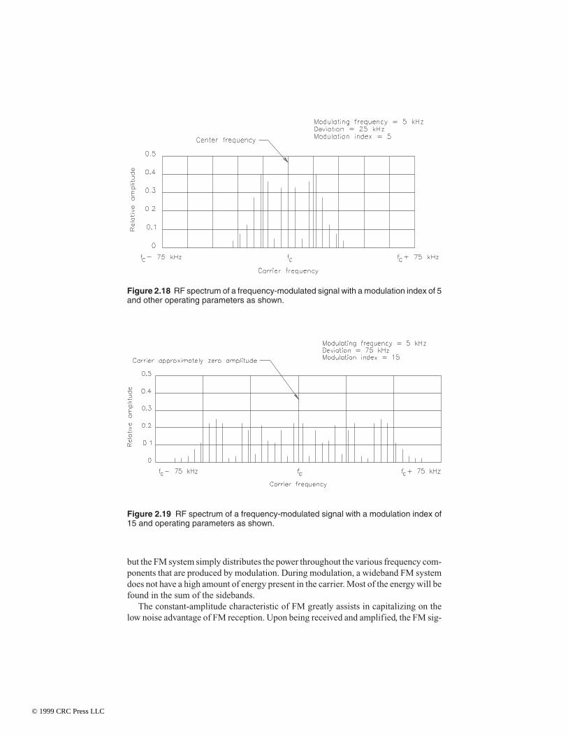
but the FM system simply distributes the power throughout the various frequency com-ponents that are produced by modulation. During modulation, a wideband FM systemdoes not have a high amount of energy present in the carrier. Most of the energy will befound in the sum of the sidebands.
The constant-amplitude characteristic of FM greatly assists in capitalizing on thelow noise advantage of FM reception. Upon being received and amplified, the FM sig-
Figure 2.18 RF spectrum of a frequency-modulated signal with a modulation index of 5and other operating parameters as shown.
Figure 2.19 RF spectrum of a frequency-modulated signal with a modulation index of15 and operating parameters as shown.
© 1999 CRC Press LLC

nal normally is clipped to eliminate all amplitude variations above a certain threshold.This removes noise picked up by the receiver as a result of man-made or atmosphericsignals. It is not possible (generally speaking) for these random noise sources to changethe frequency of the desired signal; they can affect only its amplitude. The use of hardlimiting in the receiver will strip off such interference.
2.3.2 Phase Modulation
In a phase modulation (PM) system, intelligence is conveyed by varying the phase ofthe RF wave. Phase modulation is similar in many respects to frequency modulation,except in the interpretation of the modulation index. In the case of PM, the modula-tion index depends only on the amplitude of the modulation; MI is independent of thefrequency of the modulating signal. It is apparent, therefore, that the phase-modulatedwave contains the same sideband components as the FM wave and, if the modulationindices in the two cases are the same, the relative amplitudes of these different com-ponents also will be the same.
The modulation parameters of a PM system relate as follows:
∆f m fp m= × (2.13)
Where:∆f = frequency deviation of the carriermp = phase shift of the carrierfm = modulating frequency
In a phase-modulated wave, the phase shift mp is independent of the modulating fre-quency; the frequency deviation ∆f is proportional to the modulating frequency. In con-trast, with a frequency-modulated wave, the frequency deviation is independent ofmodulating frequency. Therefore, a frequency-modulated wave can be obtained from aphase modulator by making the modulating voltage applied to the phase modulator in-versely proportional to frequency. This can be readily achieved in hardware.
2.3.3 Modifying FM Waves
When a frequency-modulated wave is passed through a harmonic generator, the effectis to increase the modulation index by a factor equal to the frequency multiplicationinvolved. Similarly, if the frequency-modulated wave is passed through a frequencydivider, the effect is to reduce the modulation index by the factor of frequency divi-sion. Thus, the frequency components contained in the wave—and, consequently, thebandwidth of the wave—will be increased or decreased, respectively, by frequencymultiplication or division. No distortion in the nature of the modulation is introducedby the frequency change.
When an FM wave is translated in the frequency spectrum by heterodyne action, themodulation index—hence the relative positions of the sideband frequencies and thebandwidths occupied by them—remains unchanged.
© 1999 CRC Press LLC

2.3.4 Preemphasis and Deemphasis
The FM transmission/reception system offers significantly better noise-rejectioncharacteristics than AM. However, FM noise rejection is more favorable at low modu-lating frequencies than at high frequencies because of the reduction in the number ofsidebands at higher frequencies. To offset this problem, the input signal to the FMtransmitter may be preemphasized to increase the amplitude of higher-frequency sig-nal components in normal program material. FM receivers utilize complementarydeemphasis to produce flat overall system frequency response.
FM broadcasting, for example, uses a 75 µs preemphasis curve, meaning that thetime constant of the resistance-inductance (RL) or resistance-capacitance (RC) circuitused to provide the boost of high frequencies is 75 µs. Other values of preemphasis areused in different types of FM communications systems. Figure 2.20 shows three com-mon preemphasis curves.
2.3.5 Modulation Circuits
Early FM transmitters used reactance modulators that operated at a low frequency.The output of the modulator then was multiplied to reach the desired output fre-quency. This approach was acceptable for some applications and unsuitable for oth-ers. Modern FM systems utilize what is referred to as direct modulation; that is, the
Figure 2.20 Preemphasis curves for time constants of 50, 75, and 100 µs.
© 1999 CRC Press LLC
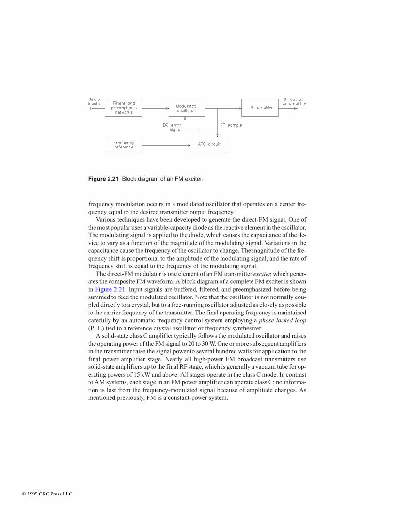
frequency modulation occurs in a modulated oscillator that operates on a center fre-quency equal to the desired transmitter output frequency.
Various techniques have been developed to generate the direct-FM signal. One ofthe most popular uses a variable-capacity diode as the reactive element in the oscillator.The modulating signal is applied to the diode, which causes the capacitance of the de-vice to vary as a function of the magnitude of the modulating signal. Variations in thecapacitance cause the frequency of the oscillator to change. The magnitude of the fre-quency shift is proportional to the amplitude of the modulating signal, and the rate offrequency shift is equal to the frequency of the modulating signal.
The direct-FM modulator is one element of an FM transmitter exciter, which gener-ates the composite FM waveform. A block diagram of a complete FM exciter is shownin Figure 2.21. Input signals are buffered, filtered, and preemphasized before beingsummed to feed the modulated oscillator. Note that the oscillator is not normally cou-pled directly to a crystal, but to a free-running oscillator adjusted as closely as possibleto the carrier frequency of the transmitter. The final operating frequency is maintainedcarefully by an automatic frequency control system employing a phase locked loop(PLL) tied to a reference crystal oscillator or frequency synthesizer.
A solid-state class C amplifier typically follows the modulated oscillator and raisesthe operating power of the FM signal to 20 to 30 W. One or more subsequent amplifiersin the transmitter raise the signal power to several hundred watts for application to thefinal power amplifier stage. Nearly all high-power FM broadcast transmitters usesolid-state amplifiers up to the final RF stage, which is generally a vacuum tube for op-erating powers of 15 kW and above. All stages operate in the class C mode. In contrastto AM systems, each stage in an FM power amplifier can operate class C; no informa-tion is lost from the frequency-modulated signal because of amplitude changes. Asmentioned previously, FM is a constant-power system.
Figure 2.21 Block diagram of an FM exciter.
© 1999 CRC Press LLC

Direct-FM Modulator
Many types of circuits have been used to produce a direct-FM signal [7]. In each case,a reactance device is used to shunt capacitive or inductive reactance across an oscilla-tor. The value of capacitive or inductive reactance is made to vary as the amplitude ofthe modulating signal varies. Because the reactive load is placed across an oscillator’stuned circuit, the frequency of the oscillator will therefore shift by a predeterminedamount, thereby creating an FM signal.
A typical example of a reactance modulator is illustrated in Figure 2.22. The circuituses a field-effect transistor (FET), where the modulating signal is applied to the modu-lator through C1. The actual components that affect the overall reactance consist of R1
and C2. Typically, the value of C2 is small as this is the input capacitance to the FET,which may only be a few picofarads. However, this capacitance will generally be muchlarger by a significant amount as a result of the Miller effect. Capacitor C3 has no signif-icant effect on the reactance of the modulator; it is strictly a blocking capacitor thatkeeps dc from changing the gate bias of the FET.
To further understand the performance of the reactance modulator, the equivalentcircuit of Figure 2.22 is represented in Figure 2.23. The FET is represented as a currentsource, gmVg, with the internal drain resistance, rd. The impedances Z1 and Z2 are a com-bination of resistance and capacitive reactance, which are designed to provide a 90ºphase shift.
Using vector diagrams, we can analyze the phase relationship of the reactance mod-ulator. Referring to Figure 2.22, the resistance of R1 is typically high compared to thecapacitive reactance of C2. The R1C2 circuit is then resistive. Because this circuit is re-sistive, the current, IAB, that flows through it, is in phase with the voltage VAB. Voltage VAB
is also across R1C2 (or Z1Z2 in Figure 2.23). This is true because current and voltage tendto be in phase in a resistive network. However, voltage VC2, which is across C2, is out ofphase with IAB. This is because the voltage that is across a capacitor lags behind its cur-rent by 90°. (See Figure 2.24.)
Figure 2.22 Simplifiedreactance modulator.(From [7]. Used withpermission.)
© 1999 CRC Press LLC

VCO Direct-FM Modulator
One of the more common direct-FM modulation techniques uses an analog voltagecontrolled oscillator (VCO) in a phase locked loop arrangement [7]. In this configu-ration, shown in Figure 2.25, a VCO produces the desired carrier frequency thatis—in turn—modulated by applying the input signal to the VCO input via a variactordiode. The variactor is used to vary the capacitance of an oscillator tank circuit.Therefore, the variactor behaves as a variable capacitor whose capacitance changes asthe signal voltage across it changes. As the input capacitance of the VCO is varied by
Figure 2.23 Equiva-lent circuit of thereactance modulator.(From [7]. Used withpermission.)
Figure 2.24 Vectordiagram of areactance modulatorproducing FM. Note:Vg = VC2. (From [7].Used with permis-sion.)
Figure 2.25 Volt-age-controlled di-rect-FM modulator.(From [7]. Used withpermission.)
© 1999 CRC Press LLC

the variactor, the output frequency of the VCO is shifted, which produces a direct-FMmodulated signal.
FM Power Amplifiers
Nearly all high-power FM transmitters employ cavity designs. The 1/4-wavelengthcavity is the most common. The design is simple and straightforward. A number ofvariations can be found in different transmitters, but the underlying theory of opera-tion is the same. The goal of any cavity amplifier is to simulate a resonant tank circuitat the operating frequency and provide a means to couple the energy in the cavity tothe transmission line.
A typical 1/4-wave cavity is shown in Figure 2.26. The plate of the tube connects di-rectly to the inner section (tube) of the plate-blocking capacitor. The blocking capacitorcan be formed in one of several ways. In at least one design, it is made by wrapping theoutside surface of the inner tube conductor with multiple layers of insulating film. Theexhaust chimney/inner conductor forms the other element of the blocking capacitor.The cavity walls form the outer conductor of the 1/4-wave transmission line circuit.The dc plate voltage is applied to the PA tube by a cable routed inside the exhaust chim-
Figure 2.26 Mechanical layout of a common type of 1/4-wave PA cavity for FM service.
© 1999 CRC Press LLC

ney and inner tube conductor. In this design, the screen-contact fingerstock ringmounts on a metal plate that is insulated from the grounded cavity deck by a blockingcapacitor. This hardware makes up the screen-blocker assembly. The dc screen voltagefeeds to the fingerstock ring from underneath the cavity deck using an insulatedfeedthrough.
Some transmitters that employ the 1/4-wave cavity design use a grounded-screenconfiguration in which the screen-contact fingerstock ring is connected directly to thegrounded cavity deck. The PA cathode then operates at below ground potential (in otherwords, at a negative voltage), establishing the required screen voltage for the tube.
Coarse-tuning of the cavity is accomplished by adjusting the cavity length. The topof the cavity (the cavity shorting deck) is fastened by screws or clamps and can be raisedor lowered to set the length of the assembly for the particular operating frequency.Fine-tuning is accomplished by a variable-capacity plate-tuning control built into thecavity. In the example shown in Figure 2.26, one plate of this capacitor—the stationaryplate—is fastened to the inner conductor just above the plate-blocking capacitor. Themovable tuning plate is fastened to the cavity box, the outer conductor, and is linkedmechanically to the front-panel tuning control. This capacity shunts the inner conduc-tor to the outer conductor and varies the electrical length and resonant frequency of thecavity.
The theory of operation of cavity amplifier systems is discussed in Section 4.3.
2.4 Pulse ModulationThe growth of digital processing and communications has led to the development ofmodulation systems tailor-made for high-speed, spectrum-efficient transmission. In apulse modulation system, the unmodulated carrier usually consists of a series of re-current pulses. Information is conveyed by modulating some parameter of the pulses,such as amplitude, duration, time of occurrence, or shape. Pulse modulation is basedon the sampling principle, which states that a message waveform with a spectrum offinite width can be recovered from a set of discrete samples if the sampling rate ishigher than twice the highest sampled frequency (the Nyquist criteria). The samplesof the input signal are used to modulate some characteristic of the carrier pulses.
2.4.1 Digital Modulation Systems
Because of the nature of digital signals (on or off), it follows that the amplitude of thesignal in a pulse modulation system should be one of two heights (present or ab-sent/positive or negative) for maximum efficiency. Noise immunity is a significantadvantage of such a system. It is necessary for the receiving system to detect only thepresence or absence (or polarity) of each transmitted pulse to allow complete recon-struction of the original intelligence. The pulse shape and noise level have minimaleffect (to a point). Furthermore, if the waveform is to be transmitted over long dis-tances, it is possible to regenerate the original signal exactly for retransmission to thenext relay point. This feature is in striking contrast to analog modulation systems inwhich each modulation step introduces some amount of noise and signal corruption.
© 1999 CRC Press LLC

In any practical digital data system, some corruption of the intelligence is likely tooccur over a sufficiently large span of time. Data encoding and manipulation schemeshave been developed to detect and correct or conceal such errors. The addition of er-ror-correction features comes at the expense of increased system overhead and (usu-ally) slightly lower intelligence throughput.
2.4.2 Pulse Amplitude Modulation
Pulse amplitude modulation (PAM) is one of the simplest forms of data modulation.PAM departs from conventional modulation systems in that the carrier exists as a se-ries of pulses, rather than as a continuous waveform. The amplitude of the pulse trainis modified in accordance with the applied modulating signal to convey intelligence,as illustrated in Figure 2.27. There are two primary forms of PAM sampling:
• Natural sampling (or top sampling), where the modulated pulses follow the am-plitude variation of the sampled time function during the sampling interval.
• Instantaneous sampling (or square-topped sampling), where the amplitude of thepulses is determined by the instantaneous value of the sampled time function cor-responding to a single instant of the sampling interval. This “single instant” maybe the center or edge of the sampling interval.
There are two common methods of generating a PAM signal:
• Variation of the amplitude of a pulse sequence about a fixed nonzero value (orpedestal). This approach constitutes double-sideband amplitude modulation.
• Double-polarity modulated pulses with no pedestal. This approach constitutesdouble-sideband suppressed carrier modulation.
2.4.3 Pulse Time Modulation (PTM)
A number of modulating schemes have been developed to take advantage of the noiseimmunity afforded by a constant amplitude modulating system. Pulse time modula-tion (PTM) is one of those systems. In a PTM system, instantaneous samples of theintelligence are used to vary the time of occurrence of some parameter of the pulsedcarrier. Subsets of the PTM process include:
• Pulse duration modulation (PDM), where the time of occurrence of either theleading or trailing edge of each pulse (or both pulses) is varied from itsunmodulated position by samples of the input modulating waveform. PDM alsomay be described as pulse length or pulse width modulation (PWM).
• Pulse position modulation (PPM), where samples of the modulating input signalare used to vary the position in time of pulses, relative to the unmodulated wave-form. Several types of pulse time modulation waveforms are shown in Figure2.28.
© 1999 CRC Press LLC

Figure 2.27 Pulse amplitude modulation waveforms: (a) modulating signal; (b)square-topped sampling, bipolar pulse train; (c) topped sampling, bipolar pulse train; (d)square-topped sampling, unipolar pulse train; (e) top sampling, unipolar pulse train.
(a)
(b)
(c)
(d)
(e)
© 1999 CRC Press LLC

• Pulse frequency modulation (PFM), where samples of the input signal are used tomodulate the frequency of a series of carrier pulses. The PFM process is illus-trated in Figure 2.29.
It should be emphasized that all of the pulse modulation systems discussed thus farmay be used with both analog and digital input signals. Conversion is required for eithersignal into a form that can be accepted by the pulse modulator.
Figure 2.28 Pulse time modulation waveforms: (a) modulating signal and sam-ple-and-hold (S/H) waveforms, (b) sawtooth waveform added to S/H, (c) leading-edgePTM, (d) trailing-edge PTM.
(a)
(b)
(c)
(d)
© 1999 CRC Press LLC

2.4.4 Pulse Code Modulation
The pulse modulation systems discussed previously are unencoded systems. Pulsecode modulation (PCM) is a scheme wherein the input signal is quantized into dis-crete steps and then sampled at regular intervals (as in conventional pulse modula-tion). In the quantization process, the input signal is sampled to produce a code repre-senting the instantaneous value of the input within a predetermined range of values.Figure 2.30 illustrates the concept. Only certain discrete levels are allowed in the
Figure 2.29 Pulse frequency modulation.
Figure 2.30 The quantization process.
© 1999 CRC Press LLC

quantization process. The code is then transmitted over the communications systemas a pattern of pulses.
Quantization inherently introduces an initial error in the amplitude of the samplestaken. This quantization error is reduced as the number of quantization steps is in-creased. In system design, tradeoffs must be made regarding low quantization error,hardware complexity, and occupied bandwidth. The greater the number of quantizationsteps, the wider the bandwidth required to transmit the intelligence or, in the case ofsome signal sources, the slower the intelligence must be transmitted.
In the classic design of a PCM encoder, the quantization steps are equal. Thequantization error (or quantization noise) usually can be reduced, however, through theuse of nonuniform spacing of levels. Smaller quantization steps are provided forweaker signals, and larger steps are provided near the peak of large signals.Quantization noise is reduced by providing an encoder that is matched to the level dis-tribution (probability density) of the input signal.
Nonuniform quantization typically is realized in an encoder through processing ofthe input (analog) signal to compress it to match the desired nonuniformity. After com-pression, the signal is fed to a uniform quantization stage.
2.4.5 Delta Modulation
Delta modulation (DM) is a coding system that measures changes in the direction ofthe input waveform, rather than the instantaneous value of the wave itself. Figure 2.31illustrates the concept. The clock rate is assumed to be constant. Transmitted pulsesfrom the pulse generator are positive if the signal is changing in a positive direction;they are negative if the signal is changing in a negative direction.
As with the PCM encoding system, quantization noise is a parameter of concern forDM. Quantization noise can be reduced by increasing the sampling frequency (thepulse generator frequency). The DM system has no fixed maximum (or minimum) sig-nal amplitude. The limiting factor is the slope of the sampled signal, which must notchange by more than one level or step during each pulse interval.
2.4.6 Digital Coding Systems
A number of methods exist to transmit digital signals over long distances in analogtransmission channels. Some of the more common systems include:
• Binary on-off keying (BOOK), a method by which a high-frequency sinusoidalsignal is switched on and off corresponding to 1 and 0 (on and off) periods in theinput digital data stream. In practice, the transmitted sinusoidal waveform doesnot start or stop abruptly, but follows a predefined ramp up or down.
• Binary frequency-shift keying (BFSK), a modulation method in which a continu-ous wave is transmitted that is shifted between two frequencies, representing 1sand 0s in the input data stream. The BFSK signal may be generated by switchingbetween two oscillators (set to different operating frequencies) or by applying abinary baseband signal to the input of a voltage-controlled oscillator (VCO). The
© 1999 CRC Press LLC

transmitted signals often are referred to as a mark (binary digit 1) or a space (bi-nary digit 0). Figure 2.32 illustrates the transmitted waveform of a BFSK system.
• Binary phase-shift keying (BPSK), a modulating method in which the phase ofthe transmitted wave is shifted 180° in synchronism with the input digital signal.The phase of the RF carrier is shifted by π/2 radians or –π/2 radians, dependingupon whether the data bit is a 0 or a 1. Figure 2.33 shows the BPSK transmittedwaveform.
Figure 2.31 Delta modulation waveforms: (a) modulating signal, (b) quantized modu-lating signal, (c) pulse train, (d) resulting delta modulation waveform.
(a)
(b)
(c)
(d)
© 1999 CRC Press LLC

• Quadriphase-shift keying (QPSK), a modulation scheme similar to BPSK exceptthat quaternary modulation is employed, rather than binary modulation. QPSKrequires half the bandwidth of BPSK for the same transmitted data rate.
2.4.7 Baseband Digital Pulse Modulation
After the input samples have been quantized, they are transmitted through a channel,received, and converted back to their approximate original form [8].The format (mod-ulation scheme) applied to the quantized samples is determined by a number of fac-tors, not the least of which is the channel through which the signal passes. A numberof different formats are possible and practical.
Figure 2.32 Binary FSK waveform.
Figure 2.33 Binary PSK waveform.
© 1999 CRC Press LLC

Several common digital modulation formats are shown in Figure 2.34. The first (a)is referred to as non-return-to-zero (NRZ) polar because the waveform does not returnto zero during each signaling interval, but switches from +V to –V, or vice versa, at theend of each signaling interval (NRZ unipolar uses the levels V and 0). On the otherhand, the unipolar return-to-zero (RZ) format, shown in (b) returns to zero in each sig-naling interval. Because bandwidth is inversely proportional to pulse duration, it is ap-parent that RZ requires twice the bandwidth that NRZ does. Also, RZ has a nonzero dccomponent, whereas NRZ does not necessarily have a nonzero component (unlessthere are more 1s than 0s or vice versa). An advantage of RZ over NRZ is that a pulsetransition is guaranteed in each signaling interval, whereas this is not the case for NRZ.Thus, in cases where there are long strings of 1s or 0s, it may be difficult to synchronizethe receiver to the start and stop times of each pulse in NRZ-based systems. A very im-portant modulation format from the standpoint of synchronization considerations isNRZ-mark, also known as differential encoding, where an initial reference bit is chosenand a subsequent 1 is encoded as a change from the reference and a 0 is encoded as nochange. After the initial reference bit, the current bit serves as a reference for the nextbit, and so on. An example of this modulation format is shown in (c).
Manchester is another baseband data modulation format that guarantees a transitionin each signaling interval and does not have a dc component. Also known as biphase orsplit phase, this scheme is illustrated in (d). The format is produced by ORing the dataclock with an NRZ-formatted signal. The result is a + to – transition for a logic 1, and a –to + zero crossing for a logic 0.
A number of other data formats have been proposed and employed in the past, butfurther discussion is beyond the scope of this chapter.
2.4.8 Spread Spectrum Systems
As the name implies, a spread spectrum system requires a frequency range substan-tially greater than the basic information-bearing signal. Spread spectrum systemshave some or all of the following properties:
• Low interference to other communications systems
• Ability to reject high levels of external interference
• Immunity to jamming by hostile forces
• Provision for secure communications paths
• Operability over multiple RF paths
Spread spectrum systems operate with an entirely different set of requirements thantransmission systems discussed previously. Conventional modulation methods are de-signed to provide for the easiest possible reception and demodulation of the transmittedintelligence. The goals of spread spectrum systems, on the other hand, are secure andreliable communications that cannot be intercepted by unauthorized persons. The mostcommon modulating and encoding techniques used in spread spectrum communica-tions include:
© 1999 CRC Press LLC

Figure 2.34 Various baseband modulation formats: (a) non-return-to zero, (b) unipolarreturn-to-zero, (c) differential encoded (NRZ-mark), (d) split phase. (From [8]. Used withpermission.)
(a)
(b)
(c)
(d)
© 1999 CRC Press LLC

• Frequency hopping, where a random or pseudorandom number (PN) sequence isused to change the carrier frequency of the transmitter. This approach has two ba-sic variations: slow frequency hopping, where the hopping rate is smaller than thedata rate, and fast frequency hopping, where the hopping rate is larger than thedata rate. In a fast frequency-hopping system, the transmission of a single piece ofdata occupies more than one frequency. Frequency-hopping systems permit mul-tiple-access capability to a given band of frequencies because each transmittedsignal occupies only a fraction of the total transmitted bandwidth.
• Time hopping, where a PN sequence is used to switch the position of a mes-sage-carrying pulse within a series of frames.
• Message corruption, where a PN sequence is added to the message before modu-lation.
• Chirp spread spectrum, where linear frequency modulation of the main carrier isused to spread the transmitted spectrum. This technique is commonly used in ra-dar and also has been applied to communications systems.
In a spread spectrum system, the signal power is divided over a large bandwidth. Thesignal, therefore, has a small average power in any single narrowband slot. This meansthat a spread spectrum system can share a given frequency band with one or morenarrowband systems. Furthermore, because of the low energy in any particular band,detection or interception of the transmission is difficult.
2.5 References1. Tate, Jeffrey P., and Patricia F. Mead, “Crystal Oscillators,” in The Electronics
Handbook, Jerry C. Whitaker (ed.), CRC Press, Boca Raton, FL, pp. 185–199,1996.
2. Frerking, M. E., Crystal Oscillator Design and Temperature Compensation, VanNostrand Reinhold, New York, 1978.
3. Dye, D. W., Proc. Phys. Soc., Vol. 38, pp. 399–457, 1926.4. Douglass, Barry G., “Thermal Noise and Other Circuit Noise,” in The Electronics
Handbook, Jerry C. Whitaker (ed.), pp. 30–36, 1996.5. Terman, F. E., Radio Engineering, 3rd ed., McGraw-Hill, New York, pg. 468, 1947.6. Kubichek, Robert, “Amplitude Modulation,” in The Electronics Handbook, Jerry C.
Whitaker (ed.), CRC Press, Boca Raton, FL, pp. 1175–1187, 1996.7. Seymour, Ken, “Frequency Modulation,” in The Electronics Handbook, Jerry C.
Whitaker (ed.), CRC Press, Boca Raton, FL, pp. 1188–1200, 1996.8. Ziemer, Rodger E., “Pulse Modulation,” in The Electronics Handbook, Jerry C.
Whitaker (ed.), CRC Press, Boca Raton, FL, pp. 1201–1212, 1996.
2.6 BibliographyBenson, K. B., and Jerry. C. Whitaker (eds.), Television Engineering Handbook,
McGraw-Hill, New York, 1986.
© 1999 CRC Press LLC

Benson, K. B., and Jerry. C. Whitaker, Television and Audio Handbook for Techni-cians and Engineers, McGraw-Hill, New York, 1989.
Crutchfield, E. B. (ed.), NAB Engineering Handbook, 8th Ed., National Association ofBroadcasters, Washington, DC, 1991.
Fink, D., and D. Christiansen (eds.), Electronics Engineers’ Handbook, 3rd Ed.,McGraw-Hill, New York, 1989.
Fink, D., and D. Christiansen (eds.), Electronics Engineers’ Handbook, 2nd Ed.,McGraw-Hill, New York, 1982.
Hulick, Timothy P., “Using Tetrodes for High Power UHF,” Proceedings of the Soci-ety of Broadcast Engineers, Vol. 4, SBE, Indianapolis, IN, pp. 52-57, 1989.
Jordan, Edward C., Reference Data for Engineers: Radio, Electronics, Computer andCommunications, 7th Ed., Howard W. Sams, Indianapolis, IN, 1985.
Laboratory Staff, The Care and Feeding of Power Grid Tubes, Varian Eimac, SanCarlos, CA, 1984.
Mendenhall, G. N., “Fine Tuning FM Final Stages,” Broadcast Engineering, IntertecPublishing, Overland Park, KS, May 1987.
Whitaker, Jerry. C., Maintaining Electronic Systems, CRC Press, Boca Raton, FL,1992.
Whitaker, Jerry. C., Radio Frequency Transmission Systems: Design and Operation,McGraw-Hill, New York, 1991.
© 1999 CRC Press LLC

Whitaker, Jerry C. “Chapter 3 – Vacuum Tube Principles” Power Vacuum Tubes Handbook 2nd Edition.Ed. Jerry C. WhitakerBoca Raton: CRC Press LLC, 2000
© 1999 CRC Press LLC

Chapter
3Vacuum Tube Principles
3.1 IntroductionA power grid tube is a device using the flow of free electrons in a vacuum to produceuseful work [1]. It has an emitting surface (the cathode), one or more grids that con-trol the flow of electrons, and an element that collects the electrons (the anode). Powertubes can be separated into groups according to the number of electrodes (grids) theycontain. The physical shape and location of the grids relative to the plate and cathodeare the main factors that determine the amplification factor (µ) and other parametersof the device (see Section 3.2.5). The physical size and types of material used to con-struct the individual elements determine the power capability of the tube. A wide vari-ety of tube designs are available to commercial and industrial users. By far the mostcommon are triodes and tetrodes.
3.2 Characteristics of ElectronsElectrons are minute, negatively charged particles that are constituents of all matter.They have a mass of 9 × 10–28 g (1/1840 that of a hydrogen atom) and a charge of 1.59× 10⁻¹⁹ coulomb. Electrons are always identical, irrespective of their source. Atomsare composed of one or more such electrons associated with a much heavier nucleus,which has a positive charge equal to the number of the negatively charged electronscontained in the atom; an atom with a full quota of electrons is electrically neutral.The differences in chemical elements arise from differences in the nucleus and in thenumber of associated electrons.
Free electrons can be produced in a number of ways. Thermonic emission is themethod normally employed in vacuum tubes (discussed in Section 3.2.2). The principleof thermonic emission states that if a solid body is heated sufficiently, some of the elec-trons that it contains will escape from the surface into the surrounding space. Electronsalso are ejected from solid materials as a result of the impact of rapidly moving elec-trons or ions. This phenomenon is referred to as secondary electron emission, becauseit is necessary to have a primary source of electrons (or ions) before the secondaryemission can be obtained (Section 3.2.3). Finally, it is possible to pull electrons directlyout of solid substances by an intense electrostatic field at the surface of the material.
© 1999 CRC Press LLC

Positive ions represent atoms or molecules that have lost one or more electrons andso have become charged bodies having the weight of the atom or molecule concerned,and a positive charge equal to the negative charge of the lost electrons. Unlike electrons,positive ions are not all alike and may differ in charge or weight, or both. They are muchheavier than electrons and resemble the molecule or atom from which they are derived.Ions are designated according to their origin, such as mercury ions or hydrogen ions.
3.2.1 Electron Optics
Electrons and ions are charged particles and, as such, have forces exerted upon themby an electrostatic field in the same way as other charged bodies. Electrons, beingnegatively charged, tend to travel toward the positive or anode electrode, while thepositively charged ions travel in the opposite direction (toward the negative or cathodeelectrode). The force F exerted upon a charged particle by an electrostatic field is pro-portional to the product of the charge e of the particle and the voltage gradient G ofthe electrostatic field [1]:
F G e= × × 10 7 (3.1)
Where:F = force in dynesG = voltage gradient in volts per centimetere = charge in coulombs
This force upon the ion or electron is exerted in the direction of the electrostatic fluxlines at the point where the charge is located. The force acts toward or away from thepositive terminal, depending upon whether a negative or positive charge, respectively,is involved.
The force that the field exerts on the charged particle causes an acceleration in thedirection of the field at a rate that can be calculated by the laws of mechanics where thevelocity does not approach that of light:
AF
M= (3.2)
Where:A = acceleration in centimeters per second per secondF = force in dynesm = mass in grams
The velocity an electron or ion acquires in being acted upon by an electrostatic fieldcan be expressed in terms of the voltage through which the electron (or ion) has fallen inacquiring the velocity. For velocities well below the speed of light, the relationship be-tween velocity and the acceleration voltage is:
© 1999 CRC Press LLC

vV e
m= × × ×2 10 7
(3.3)
Where:v = velocity in centimeters per second corresponding to VV = accelerating voltagee = charge in coulombsm = mass in grams
Electrons and ions move at great velocities in even moderate-strength fields. For ex-ample, an electron dropping through a potential difference of 2500 V will achieve a ve-locity of approximately one-tenth the speed of light.
Electron optics, as discussed in this section, relies on the principles of classicalphysics. While modern tube design uses computer simulation almost exclusively, thepreceding information is still valid and provides a basis for the understanding of elec-tron motion within a vacuum tube device.
Magnetic Field Effects
An electron in motion represents an electric current of magnitude ev, where e is themagnitude of the charge on the electron and v is its velocity. A magnetic field accord-ingly exerts a force on a moving electron exactly as it exerts a force on an electric cur-rent in a wire. The magnitude of the force is proportional to the product of the equiva-lent current ev represented by the moving electron and the strength of the componentof the magnetic field in a direction at right angles to the motion of the electron. Theresulting force is, then, in a direction at right angles both to the direction of motion ofthe electron and to the component of the magnetic field that is producing the force. Asa result, an electron entering a magnetic field with a high velocity will follow acurved path. Because the acceleration of the electron that the force of the magneticfield produces is always at right angles to the direction in which the electron is travel-ing, an electron moving in a uniform magnetic field will follow a circular path. Theradius of this circle is determined by the strength of the magnetic field and the speedof the electron moving through the field.
When an electron is subjected to the simultaneous action of both electric and mag-netic fields, the resulting force acting on the electron is the vector sum of the force re-sulting from the electric field and the force resulting from the magnetic field, each con-sidered separately.
Magnetic fields are not used for conventional power grid tubes. Microwave powertubes, on the other hand, use magnetic fields to confine and focus the electron stream.
3.2.2 Thermal Emission From Metals
Thermonic emission is the phenomenon of an electric current leaving the surface of amaterial as the result of thermal activation. Electrons with sufficient thermal energyto overcome the surface-potential barrier escape from the surface of the material. This
© 1999 CRC Press LLC

thermally emitted electron current increases with temperature because more electronshave sufficient energy to leave the material.
The number of electrons released per unit area of an emitting surface is related to theabsolute temperature of the emitting material and a quantity b that is a measure of thework an electron must perform in escaping through the surface, according to the equa-tion [1]:
I A Tb
T= −2 ε (3.4)
Where:T = absolute temperature of the emitting materialb = the work an electron must perform in escaping the emitter surfaceI = electron current in amperes per square centimeterA = a constant (value varies with type of emitter)
The exponential term in the equation accounts for most of the variation in emissionwith temperature. The temperature at which the electron current becomes appreciableis accordingly determined almost solely by the quantity b. Figure 3.1 plots the emis-sion resulting from a cathode operated at various temperatures.
Thermal electron emission can be increased by applying an electric field to the cath-ode. This field lowers the surface-potential barrier, enabling more electrons to escape.This field-assisted emission is known as the Schottky effect.
Figure 3.2 illustrates common heater-cathode structures for power tubes.
3.2.3 Secondary Emission
Almost all metals and some insulators will emit low-energy electrons (secondaryelectrons) when bombarded by other energetic electrons. The number of secondaryelectrons emitted per primary electron is determined by the velocity of the primarybombarding electrons and the nature and condition of the material composing the sur-face being bombarded. Figure 3.3 illustrates a typical relationship for two types ofsurfaces. As shown in the figure, no secondary electrons are produced when the pri-mary velocity is low. However, with increasing potential (and consequently higher ve-locity), the ratio of secondary to primary electrons increases, reaching a maximumand then decreasing. With pure metal surfaces, the maximum ratio of secondary toprimary electrons ranges from less than 1 to approximately 3. Some complex surfacesbased on alkali metal compounds yield ratios of secondary to primary electrons ashigh as 5 to 10.
The majority of secondary electrons emitted from a conductive surface have rela-tively low velocity. However, a few secondary electrons usually are emitted with a ve-locity nearly equal to the velocity of the bombarding primary electrons.
For insulators, the ratio of secondary to primary electrons as a function of primaryelectron potential follows along the same lines as for metals. The net potential of the in-sulating surface being bombarded is affected by the bombardment. If the ratio of sec-ondary to primary current is less than unity, the insulator acquires a net negative charge
© 1999 CRC Press LLC

because more electrons arrive than depart. This causes the insulator to become morenegative and, finally, to repel most of the primary electrons, resulting in a blocking ac-tion. In the opposite extreme, when the ratio of secondary to primary electrons exceedsunity, the insulating surface loses electrons through secondary emission faster than
Figure 3.1 Variation of electron emission as a function of absolute temperature for athoriated-tungsten emitter.
Figure 3.2 Common types of heater and cathode structures. (From [2]. Used with per-mission.)
© 1999 CRC Press LLC

they arrive; the surface becomes increasingly positive. This action continues until thesurface is sufficiently positive that the ratio of secondary to primary electrons de-creases to unity as a result of the increase in the velocity of the bombarding electrons, oruntil the surface is sufficiently positive that it attracts back into itself a significant num-ber of secondary electrons. This process makes the number of electrons gained from allsources equal to the number of secondary electrons emitted.
3.2.4 Diode
A diode is a two-electrode vacuum tube containing a cathode, which emits electronsby thermonic emission, surrounded by an anode (or plate). (See Figure 3.4) Such atube is inherently a rectifier because when the anode is positive, it attracts electrons;current, therefore, passes through the tube. When the anode is negative, it repels theelectrons and no current flows.
The typical relationship between anode voltage and current flowing to the positiveanode is shown in Figure 3.5. When the anode voltage is sufficiently high, electrons are
Figure 3.3 Ratio of secondary emission current to primary current as a function of pri-mary electron velocity.
© 1999 CRC Press LLC

drawn from the cathode as rapidly as they are emitted. The anode current is then limitedby the electron emission of the cathode and, therefore, depends upon cathode tempera-ture rather than anode voltage.
At low anode voltages, however, plate current is less than the emission of which thecathode is capable. This occurs because the number of electrons in transit between thecathode and plate at any instant cannot exceed the number that will produce a negativespace charge, which completely neutralizes the attraction of the positive plate upon theelectrons just leaving the cathode. All electrons in excess of the number necessary to
Figure 3.5 Anode current as a function of anode voltage in a two-electrode tube forthree cathode temperatures.
(a) (b)
Figure 3.4 Vacuum diode: (a) directly heated cathode, (b) indirectly heated cathode.(From [2]. Used with permission.)
© 1999 CRC Press LLC

neutralize the effects of the plate voltage are repelled into the cathode by the negativespace charge of the electrons in transit; this situation applies irrespective of how manyexcess electrons the cathode emits. When the plate current is limited in this way byspace charge, plate current is determined by plate potential and is substantially inde-pendent of the electron emission of the cathode.
Detailed examination of the space-charge situation will reveal that the negativecharge of the electrons in transit between the cathode and the plate is sufficient to givethe space in the immediate vicinity of the cathode a slight negative potential with re-spect to the cathode. The electrons emitted from the cathode are projected out into thisfield with varying emission velocities. The negative field next to the cathode causes theemitted electrons to slow as they move away from the cathode, and those having a lowvelocity of emission are driven back into the cathode. Only those electrons having thehighest velocities of emission will penetrate the negative field near the cathode andreach the region where they are drawn toward the positive plate. The remainder (thoseelectrons having low emission velocities) will be brought to a stop by the negative fieldadjacent to the cathode and will fall back into the cathode.
The energy that is delivered to the tube by the source of anode voltage is first ex-pended in accelerating the electrons traveling from the cathode to the anode; it is con-verted into kinetic energy. When these swiftly moving electrons strike the anode, thiskinetic energy is then transformed into heat as a result of the impact and appears at theanode in the form of heat that must be radiated to the walls of the tube.
The basic function of a vacuum tube diode—to rectify an ac voltage—has been su-perseded by solid-state devices. An understanding of how the diode operates, however,is important in understanding the operation of triodes, tetrodes, and pentodes.
3.2.5 Triode
The power triode is a three-element device commonly used in a wide variety of RFgenerators. Triodes have three internal elements: the cathode, control grid, and plate.Most tubes are cylindrically symmetrical. The filament or cathode structure, the grid,and the anode all are cylindrical in shape and are mounted with the axis of each cylin-der along the center line of the tube, as illustrated in Figure 3.6.
The grid normally is operated at a negative potential with respect to the cathode, andso attracts no electrons. However, the extent to which it is negative affects the electro-static field in the vicinity of the cathode and, therefore, controls the number of electronsthat pass between the grid and the plate. The grid, in effect, functions as an imperfectelectrostatic shield. It allows some, but not all, of the electrostatic flux from the anodeto leak between its wires. The number of electrons that reach the anode in a triode tubeunder space-charge-limited conditions is determined almost solely by the electrostaticfield near the cathode; the field in the rest of the interelectrode space has little effect.This phenomenon results because the electrons near the cathode are moving slowlycompared with the electrons that have traveled some distance toward the plate. The re-sult of this condition is that the volume density of electrons in proportion to the rate offlow is large near the cathode and low in the remainder of the interelectrode space. Thetotal space charge of the electrons in transit toward the plate, therefore, consists almost
© 1999 CRC Press LLC
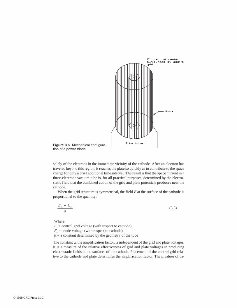
solely of the electrons in the immediate vicinity of the cathode. After an electron hastraveled beyond this region, it reaches the plate so quickly as to contribute to the spacecharge for only a brief additional time interval. The result is that the space current in athree-electrode vacuum tube is, for all practical purposes, determined by the electro-static field that the combined action of the grid and plate potentials produces near thecathode.
When the grid structure is symmetrical, the field E at the surface of the cathode isproportional to the quantity:
E Ec b+µ
(3.5)
Where:Ec = control grid voltage (with respect to cathode)Eb = anode voltage (with respect to cathode)µ = a constant determined by the geometry of the tube
The constant µ, the amplification factor, is independent of the grid and plate voltages.It is a measure of the relative effectiveness of grid and plate voltages in producingelectrostatic fields at the surfaces of the cathode. Placement of the control grid rela-tive to the cathode and plate determines the amplification factor. The µ values of tri-
Figure 3.6 Mechanical configura-tion of a power triode.
© 1999 CRC Press LLC

odes generally range from 5 to 200. Key mathematical relationships include the fol-lowing:
µ =∆∆
E
Eb
c1
(3.6)
RE
Ip
b
b
=∆∆
(3.7)
SI
Em
b
c
=∆
∆ 1
(3.8)
Where:µ = amplification factor (with plate current held constant)Rp = dynamic plate resistanceSm = transconductance (also may be denoted Gm)Eb = total instantaneous plate voltageEc1 = total instantaneous control grid voltageIb = total instantaneous plate current
The total cathode current of an ideal triode can be determined from the equation:
I EE
k cb= +
µ
32
(3.9)
Where:Ik = cathode currentK = a constant determined by tube dimensionsEc = grid voltageEb = plate voltageµ = amplification factor
Figure 3.7 plots plate and grid current as a function of plate voltage at various gridvoltages for a triode with a µof 12. The tube, a 304TL, is a classic design and, while notused in new equipment, provides a common example of the relationship between theparameters plotted. Figure 3.8 plots the same parameters for a tube with a µ of 20. Ob-serve how much more plate current at a given plate voltage can be obtained from the304TL (µ = 12) without driving the grid into the positive grid region. Note also howmuch more bias voltage is required for the 304TL to cut the plate current off at somegiven plate voltage. With this increased bias, there is a corresponding increase in gridvoltage swing to drive up the zero grid voltage point on the curve. Low-µ tubes havelower voltage gain by definition. This fact can be seen by comparing Figures 3.7 and3.8.
© 1999 CRC Press LLC

Triodes with a µof 20 to 50 generally are used in conventional RF amplifiers and os-cillators. High-µ triodes (200 or more) may be designed so that the operating bias iszero, as depicted in Figure 3.9. These zero-bias triodes are available with plate dissipa-tion ratings of 400 W to 10 kW or more. The zero-bias triode commonly is used ingrounded-grid amplification. The tube offers good power gain and circuit simplicity.No bias power source is required. Furthermore, no protection circuits for loss of bias ordrive are needed. Despite these attributes, present-day use of the zero-bias triode is lim-ited.
Low- and medium-µ devices usually are preferred for induction heating applica-tions because of the wide variations in load that an induction or dielectric heating oscil-lator normally works into. Such tubes exhibit lower grid-current variation with a chang-ing load. The grid current of a triode with a µ of 20 will rise substantially less under alight- or no-load condition than a triode with a µ of 40. High-µ triode oscillators can bedesigned for heating applications, but extra considerations must be given to current riseunder no-load conditions.
Vacuum tubes specifically designed for induction heating are available, intended foroperation under adverse conditions. The grid structure is ruggedized with ample dissi-
Figure 3.7 Constant-current characteristics for a triode with a µ of 12.
© 1999 CRC Press LLC

Figure 3.8 Constant-current characteristics for a triode with a µ of 20.
Figure 3.9 Grounded-grid constant-current characteristics for a zero-bias triode with aµ of 200.
© 1999 CRC Press LLC

pation capability to deal with wide variations in load. As the load decreases, grid dissi-pation increases.
Triodes also are manufactured with the cathode, grid, and anode in the shape of a flatsurface, as shown in Figure 3.10. Tubes so constructed are called planar triodes. Thisconstruction technique permits operation at high frequencies. The close spacing re-duces electron transit time, allowing the tube to be used at high frequencies (up to 3GHz or so). The physical construction of planar triodes results in short lead lengths,which reduces lead inductance. Planar triodes are used in both continuous wave (CW)and pulsed modes. The contacting surfaces of the planar triode are arranged for easy in-tegration into coaxial and waveguide resonators.
3.2.6 Tetrode
The tetrode is a four-element tube with two grids. The control grid serves the samepurpose as the grid in a triode, while a second (screen) grid with the same number ofvertical elements (bars) as the control grid is mounted between the control grid andthe anode. The grid bars of the screen grid are mounted directly behind the con-trol-grid bars, as observed from the cathode surface, and serve as a shield or screenbetween the input circuit and the output circuit of the tetrode. The principal advan-tages of a tetrode over a triode include:
• Lower internal plate-to-grid feedback.
Figure 3.10 Internal configuration of a planar triode.
© 1999 CRC Press LLC

• Lower drive power requirements. In most cases, the driving circuit need supplyonly 1 percent of the output power.
• More efficient operation. Tetrodes allow the design of compact, simple, flexibleequipment with little spurious radiation and low intermodulation distortion.
Plate current is almost independent of plate voltage in a tetrode. Figure 3.11 plotsplate current as a function of plate voltage at a fixed screen voltage and various gridvoltages. In an ideal tetrode, a change in plate current does not cause a change in platevoltage. The tetrode, therefore, can be considered a constant-current device. The volt-ages on the screen and control grids determine the amount of plate current.
The total cathode current of an ideal tetrode is determined by the equation:
I K EE E
k cc
s
b
p
= + +
12
32
µ µ(3.10)
Where:Ik = cathode currentK = a constant determined by tube dimensionsEc1 = control grid voltageEc2 = screen grid voltageµs = screen amplification factorµp = plate amplification factorEb = plate voltage
Figure 3.11 Tetrode plate current characteristics. Plate current is plotted as a functionof plate voltage, with grid voltages as shown.
© 1999 CRC Press LLC
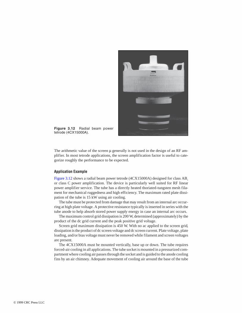
The arithmetic value of the screen µ generally is not used in the design of an RF am-plifier. In most tetrode applications, the screen amplification factor is useful to cate-gorize roughly the performance to be expected.
Application Example
Figure 3.12 shows a radial beam power tetrode (4CX15000A) designed for class AB1
or class C power amplification. The device is particularly well suited for RF linearpower amplifier service. The tube has a directly heated thoriated-tungsten mesh fila-ment for mechanical ruggedness and high efficiency. The maximum rated plate dissi-pation of the tube is 15 kW using air cooling.
The tube must be protected from damage that may result from an internal arc occur-ring at high plate voltage. A protective resistance typically is inserted in series with thetube anode to help absorb stored power supply energy in case an internal arc occurs.
The maximum control grid dissipation is 200 W, determined (approximately) by theproduct of the dc grid current and the peak positive grid voltage.
Screen grid maximum dissipation is 450 W. With no ac applied to the screen grid,dissipation is the product of dc screen voltage and dc screen current. Plate voltage, plateloading, and/or bias voltage must never be removed while filament and screen voltagesare present.
The 4CX15000A must be mounted vertically, base up or down. The tube requiresforced-air cooling in all applications. The tube socket is mounted in a pressurized com-partment where cooling air passes through the socket and is guided to the anode coolingfins by an air chimney. Adequate movement of cooling air around the base of the tube
Figure 3.12 Radial beam powertetrode (4CX15000A).
© 1999 CRC Press LLC

keeps the base and socket contact fingers at a safe operating temperature. Although themaximum temperature rating for seals and the anode is 250°C, good engineering prac-tice dictates that a safety factor be provided. Table 3.1 lists cooling parameters for thetube with the cooling air at 50°C and a maximum anode temperature of 225°C. The fig-ures given in the table apply to designs in which air passes in the base-to-anode direc-tion. Pressure drop values shown are approximate and apply to the tube/socket/chim-ney combination.
At altitudes significantly above sea level, the flow rate must be increased for equiva-lent cooling. At 5000 ft above sea level, both the flow rate and the pressure drop is in-creased by a factor of 1.20; at 10,000 ft, both flow rate and pressure drop are increasedby 1.46.
Anode and base cooling is applied before or simultaneously with filament voltageturn-on, and normally should continue for a brief period after shutdown to allow thetube to cool properly.
An outline of the principal tube dimensions is given in Figure 3.13. General specifi-cations are listed in Table 3.2.
3.2.7 Pentode
The pentode is a five-electrode tube incorporating three grids. The control and screengrids perform the same function as in a tetrode. The third grid, the suppressor grid, ismounted in the region between the screen grid and the anode. The suppressor gridproduces a potential minimum, which prevents secondary electrons from being inter-changed between the screen and plate. The pentode’s main advantages over thetetrode include:
• Reduced secondary emission effects.
• Good linearity.
• Ability to let plate voltage swing below the screen voltage without excessivescreen dissipation. This allows slightly higher power output for a given operatingplate voltage.
Table 3.1 Minimum Cooling Airflow Requirements for the 4CX15000A Power Tetrodeat Sea Level
Plate Dissipation (W) Airflow (CFM) Pressure Drop (inches ofwater)
7500 230 0.712,500 490 2.715,000 645 4.6
© 1999 CRC Press LLC

Because of the design of the pentode, plate voltage has even less effect on plate cur-rent than in the tetrode. The same total space-current equation applies to the pentodeas with the tetrode:
I K EE E
k cc
s
b
p
= + +
12
32
µ µ(3.11)
Where:Ik = cathode currentK = a constant determined by tube dimensionsEc1 = control grid voltageEc2 = screen grid voltageµs = screen amplification factorµp = plate amplification factorEb = plate voltage
The suppressor grid may be operated negative or positive with respect to the cath-ode. It also may be operated at cathode potential. It is possible to control plate current
Figure 3.13 Principal dimensions of 4CX15000A tetrode.
© 1999 CRC Press LLC

Table 3.2 General Characteristics of the 4CX15000A Power Tetrode (Courtesy ofSvetlana Electron Devices.)
Electrical CharacteristicsFilament type Thoriated-tungsten meshFilament voltage 6.3 ± 0.3 VFilament current 164 A (at 6.3 V)Amplification factor (average), grid to screen 4.5Direct interelectrode capacitance(grounded cathode)
Cin 158 pFCout 25.8 pFCpk 1.3 pF
Direct interelectrode capacitance(grounded grid)
Cin 67 pFCout 25.6 pFCgk 0.21 pF
Maximum frequency for full ratings (CW) 110 MHzMechanical Characteristics:
Length 238 mm (9.38 in)Diameter 193 mm (7.58 in)Net weight 5.8 kg (12.8 lb)Operating position Axis vertical, base up or
downMaximum operating temperature (seals/envelope) 250°CCooling method Forced airBase type Coaxial
Radio Frequency Power Amplifier (class C FM) (absolute maximum ratings)DC plate voltage 10,000 VDC screen voltage 2000 VDC grid voltage –750 VDC plate current 5.0 APlate dissipation 15 kWScreen dissipation 450 WGrid dissipation 200 W
Typical Operation (frequencies up to 110 MHz)DC plate voltage 7.5 kV dc 10.0 kV dcDC screen voltage 750 V dc 750 V dcDC grid voltage –510 V dc –550 V dcDC plate current 4.65 A dc 4.55 A dcDC screen current 0.59 A dc 0.54 A dcDC grid current 0.30 A dc 0.27 A dcPeak RF grid voltage 730 V 790 VCalculated driving power 220 W 220 WPlate dissipation 8.1 9.0 kWPlate output power 26.7 36.5 kW
© 1999 CRC Press LLC

by varying the potential on the suppressor grid. Because of this ability, a modulatingvoltage can be applied to the suppressor to achieve amplitude modulation. The requiredmodulating power is low because of the low electron interception of the suppressor.
Application Example
The 5CX1500B is a ceramic/metal power pentode designed for use as a class AB1 lin-ear amplifier or FM VHF amplifying device. The exterior of the device is shown inFigure 3.14. Basic specifications for the tube are given in Table 3.3.
The filament of the 5CX1500B is rated for 5.0 V. Filament voltage, measured at thesocket, is maintained to ±5 percent of the rated value for maximum tube life.
The rated dissipation of the control grid is 25 W. This value is approximately theproduct of dc grid current and peak positive grid voltage. Operation at bias and drivelevels near those listed in Table 3.3 will ensure safe operation.
The power dissipated by the screen grid must not exceed 75 W. Screen dissipation, incases where there is no ac applied to the screen, is the simple product of screen voltageand screen current. If the screen voltage is modulated, screen dissipation will depend onthe rms screen current and voltage. Screen dissipation is likely to rise to excessive lev-els if the plate voltage, bias voltage, or plate load are removed with filament and screenvoltages applied. Suitable protective means must be provided to limit screen dissipa-tion to 75 W in the event of a circuit failure.
The rated dissipation of the suppressor grid is 25 W. Suppressor current is zero ornearly zero for all typical operating conditions specified in Table 3.3. The 5CX1500B
Figure 3.14 5CX1500B powerpentode device.
© 1999 CRC Press LLC

Electrical CharacteristicsFilament type Thoriated-tungsten meshFilament voltage 5.0 ± 0.25 VFilament current 38.5 A (at 5.0 V)Transconductance (avg.), Ib = 1.0 A dc, Ec2 = 500V dc
24,000 µmhos
Amplification factor (average), grid to screen 5.5Direct interelectrode ca-pacitance (grounded cath-ode)
Input 75 pFOutput 17.8 pFFeedback 0.20 pF
Frequency (maximum) CW 110 MHzMechanical Characteristics
Cooling method Forced airBase Ring and breechblockRecommended air system socket SK-840 seriesRecommended (air) chimney SK-806Operating position Axis vertical, base down or upMaximum operating temperature 250°CMaximum dimensions Length 130 mm (5.2 in)
Diameter 85.6 mm (3.37 in)Net weight 850 gm (30 oz)Radio Frequency Linear Amplifier (class C, CW conditions) Maximum RatingsPlate voltage 5000 VScreen voltage 750 VPlate dissipation 1500 WSuppressor dissipation 25 WScreen dissipation 75 WGrid dissipation 25 W
Typical Operation (frequencies to 30 MHz)Plate voltage 3000 V dc 4500 V dcSuppressor voltage 0 0Screen voltage 500 V dc 500 V dcGrid voltage –200 V dc –200 V dcPlate current 900 mA dc 900 mA dcScreen current 94 mA dc 88 mA dcGrid current 35 mA dc 34 mA dcPeak RF grid voltage 255 V 255 VCalculated driving power 9.0 W 9.0 WPlate input power 2700 W 4050 WPlate dissipation 720 W 870 WPlate output power 1980 W 3180 W
Table 3.3 General Characteristics of the 5CX1500B Power Pentode (Courtesy ofSvetlana Electron Devices.)
© 1999 CRC Press LLC

has been designed for zero voltage operation of the suppressor grid for most applica-tions.
The plate dissipation rating of the 5CX1500B is 1500 W. The tube and associatedcircuitry should be protected against surge current in the event of an arc inside the tube.A current-limiting resistance of 10 to 25 Ωbetween the power supply and plate is suffi-cient. The resistor should be capable of withstanding the surge currents that may de-velop; it should not be used as a fuse.
Cooling requirements for the 5CX1500B follow along the same lines as for the4CX15000A discussed in the previous section. Table 3.4 lists the airflow requirementsfor the pentode. Note that the power dissipated by the device is equal to the power dissi-pated by the plate, heater, and grids (control, screen, and suppressor) combined. In thecase of the 5CX1500B, the heater and three grids account for approximately 350 W dis-sipation.
Mechanical dimensions for the 5CX1500B are given in Figure 3.15.
3.2.8 High-Frequency Operating Limits
As with most active devices, performance of a given vacuum tube deteriorates as theoperating frequency is increased beyond its designed limit. Electron transit time is asignificant factor in the upper-frequency limitation of electron tubes. A finite time istaken by electrons to traverse the space from the cathode, through the grid, and travelon to the plate. As the operating frequency increases, a point is reached at which theelectron transit-time effects become significant. This point is a function of the accel-erating voltages at the grid and anode and their respective spacings. Tubes with re-duced spacing in the grid-to-cathode region exhibit reduced transit-time effects.
A power limitation also is interrelated with the high-frequency limit of a device. Asthe operating frequency is increased, closer spacing and smaller-sized electrodes mustbe used. This reduces the power-handling capability of the tube. Figure 3.16 illustratesthe relationship.
Gridded tubes at all power levels for frequencies up to about 1 GHz are invariablycylindrical in form. At higher frequencies, planar construction is almost universal. Asthe operating frequency is increased beyond design limits, output power and efficiencyboth decrease. Figure 3.17 illustrates the relationship.
Table 3.4 Minimum Cooling Airflow Requirements for the 5CX1500B Power Tetrode
Plate Dissipation (W) Airflow (CFM) Pressure Drop (inches of water)At sea level 1000 27 0.33
1550 47 0.76At 6000 ft 1000 33 0.40
1550 58 0.95
© 1999 CRC Press LLC

Transit time typically is not a problem for power grid tubes operating below 30MHz. Depending on the application, power grid tubes can be used at 100 MHz andabove without serious consideration of transit time effects. Klystrons and other micro-wave tubes actually take advantage of transit time, as discussed in Chapter 6.
Transit-Time Effects
When class C, class B, or similar amplifier operations are carried out at frequenciessufficiently high that the transit time of the electrons is not a negligible fraction of thewaveform cycle, the following complications are observed in grid-based vacuumtubes:
• Back-heating of the cathode
• Loading of the control grid circuit as a result of energy transferred to electronsthat do not necessarily reach the grid to produce a dc grid current
• Debunching of plate current pulses
Figure 3.15 Principal dimensions of 5CX1500B pentode.
© 1999 CRC Press LLC

Figure 3.16 Continuous wave output power capability of a gridded vacuum tube.
Figure 3.17 Performance of a class C amplifier as the operating frequency is increasedbeyond the design limits of the vacuum tube.
© 1999 CRC Press LLC

• Phase differences between the plate current and the exciting voltage applied tothe control grid
Back-heating of the cathode occurs when the transit time in the grid-cathode spaceis sufficiently great to cause an appreciable number of electrons to be in transit at the in-stant the plate current pulse would be cut off in the case of low-frequency operation. Aconsiderable fraction of the electrons thus trapped in the interelectrode space are re-turned to the cathode by the negative field existing in the grid-cathode space during thecutoff portion of the cycle. These returning electrons act to heat the cathode. At veryhigh frequencies, this back-heating is sufficient to supply a considerable fraction of thetotal cathode heating required for normal operation. Back-heating may reduce the lifeof the cathode as a result of electron bombardment of the emitting surface. It alsocauses the required filament current to depend upon the conditions of operation withinthe tube.
Energy absorbed by the control grid as a result of input loading is transferred di-rectly to the electron stream in the tube. Part of this stream acts to produce back-heatingof the cathode. The remainder affects the velocity of the electrons as they arrive at theanode of the tube. This portion of the energy is not necessarily all wasted. In fact, a con-siderable percentage of it may, under favorable conditions, appear as useful output inthe tube. To the extent that this is the case, the energy supplied by the exciting voltage tothe electron stream is simply transferred directly from the control grid to the output cir-cuits of the tube without amplification.
An examination of the total time required by electrons to travel from the cathode tothe anode in a triode, tetrode, or pentode operated as a class C amplifier reveals that theresulting transit times for electrons at the beginning, middle, and end of the currentpulse will differ as the operating frequency is increased. In general, electrons traversingthe distance during the first segment of the pulse will have the shortest transit time,while those near the middle and end of the pulse will have the longest transit times, as il-lustrated in Figure 3.18. The first electrons in the pulse have a short transit time becausethey approach the plate before the plate potential is at its minimum value. Electronsnear the middle of the pulse approach the plate with the instantaneous plate potential ator near minimum and, consequently, travel less rapidly in the grid-plate space. Finally,those electrons that leave the cathode late in the current pulse (those just able to escapebeing trapped in the control grid-cathode space and returned toward the cathode) willbe slowed as they approach the grid, and so have a large transit time. The net effect is tocause the pulse of plate current to be longer than it would be in operation at a low fre-quency. This causes the efficiency of the amplifier to drop at high frequencies, becausea longer plate current pulse increases plate losses.
3.3 Vacuum Tube DesignAny particular power vacuum tube may be designed to meet a number of operatingparameters, the most important usually being high operating efficiency and highgain/bandwidth properties. Above all, the tube must be reliable and provide long op-erating life. The design of a new power tube is a lengthy process that involves com-
© 1999 CRC Press LLC

Figure 3.18 Transit-time effects in a class C amplifier: (a) control grid voltage, (b) elec-tron position as a function of time (triode case), (c) electron position as a function of time(tetrode case), (d) plate current (triode case).
(a)
(b)
(c)
(d)
© 1999 CRC Press LLC

puter-aided calculations and modeling. The design engineers must examine a laundrylist of items, including:
• Cooling: how the tube will dissipate heat generated during normal operation. Ahigh-performance tube is of little value if it will not provide long life in typical ap-plications. Design questions include whether the tube will be air-cooled or wa-ter-cooled, the number of fins the device will have, and the thickness and spacingof the fins.
• Electro-optics: how the internal elements line up to achieve the desired perfor-mance. A careful analysis must be made of what happens to the electrons in theirpaths from the cathode to the anode, including the expected power gain of thetube.
• Operational parameters: what the typical interelectrode capacitances will be,and the manufacturing tolerances that can be expected. This analysis includes:spacing variations among elements within the tube, the types of materials used inconstruction, the long-term stability of the internal elements, and the effects ofthermal cycling.
3.3.1 Device Cooling
The main factor that separates tube types is the method of cooling used: air, water, orvapor. Air-cooled tubes are common at power levels below 50 kW. A water coolingsystem, although more complicated, is more effective than air cooling—by a factor of5 to 10 or more—in transferring heat from the device. Air cooling at the 100 kW levelis virtually impossible because it is difficult to physically move enough air throughthe device (if the tube is to be of reasonable size) to keep the anode sufficiently cool.Vapor cooling provides an even more efficient method of cooling a power amplifier(PA) tube than water cooling, for a given water flow and a given power dissipation.Naturally, the complexity of the external blowers, fans, ducts, plumbing, heatexchangers, and other hardware must be taken into consideration in the selection of acooling method. Figure 3.19 shows how the choice of cooling method is related to an-ode dissipation.
Air Cooling
A typical air cooling system for a transmitter is shown in Figure 3.20. Cooling systemperformance for an air-cooled device is not necessarily related to airflow volume. Thecooling capability of air is a function of its mass, not its volume. An appropriate air-flow rate within the equipment is established by the manufacturer, resulting in a givenresistance to air movement.
The altitude of operation is also a consideration in cooling system design. As alti-tude increases, the density (and cooling capability) of air decreases. To maintain thesame cooling effectiveness, increased airflow must be provided. (Air cooling systemsare discussed in detail in Section 8.2.1.)
© 1999 CRC Press LLC

Figure 3.20 A typical transmitter PA stage cooling system.
Figure 3.19 The relationship between anode dissipation and cooling method.
© 1999 CRC Press LLC

Water Cooling
Water cooling usually is preferred over air cooling for power outputs above about 50kW. Multiple grooves on the outside of the anode, in conjunction with a cylindricaljacket, force the cooling water to flow over the surface of the anode, as illustrated inFigure 3.21.
Because the water is in contact with the outer surface of the anode, a high degree ofpurity must be maintained. A resistivity of 1 mΩ-cm (at 25°C) typically is specified bytube manufacturers. Circulating water can remove about 1 kW/cm2 of effective internalanode area. In practice, the temperature of water leaving the tube must be limited to70°C to prevent the possibility of spot boiling.
After leaving the anode, the heated water is passed through a heat exchanger where itis cooled to 30 to 40°C before being pumped back to the tube.
In typical modern water-cooled tubes, the dissipation ranges from 500 W to 1 kWper square centimeter. Water-cooled anodes have deen designed that can operate at 10kW per square centimeter and above. However, with the exception of “big science” ap-plications, dissipations this high are seldom required. (Water cooling systems are dis-cussed in detail in Section 8.2.2.)
Vapor-Phase Cooling
Vapor cooling allows the permissible output temperature of the water to rise to theboiling point, giving higher cooling efficiency compared with water cooling. Thebenefits of vapor-phase cooling are the result of the physics of boiling water. In-creasing the temperature of one gram of water from 40 to 70°C requires 30 calories ofenergy. However, transforming 1 g of water at 100°C into steam vapor requires 540calories. Thus, a vapor-phase cooling system permits essentially the same cooling ca-pacity as water cooling, but with greatly reduced water flow. Viewed from another
Figure 3.21 Water-cooled anode with groovesfor controlled water flow.
© 1999 CRC Press LLC

perspective, for the same water flow, the dissipation of the tube may be increased sig-nificantly (all other considerations being the same).
A typical vapor-phase cooling system is shown in Figure 3.22. A tube incorporatinga specially designed anode is immersed in a boiler filled with distilled water. Whenpower is applied to the tube, anode dissipation heats the water to the boiling point, con-verting the water to steam vapor. The vapor passes to a condenser, where it gives up itsenergy and reverts to a liquid state. The condensate then is returned to the boiler, com-pleting the cycle. Electric valves and interlocks are included in the system to provide foroperating safety and maintenance. A vapor-phase cooling system for a transmitter withmultiple PA tubes is shown in Figure 3.23. (Vapor-phase cooling systems are discussedin detail in Section 8.2.3.)
Special Applications
Power devices used for research applications must be designed for transient overload-ing, requiring special considerations with regard to cooling. Oil, heat pipes, refriger-ants (such as Freon), and, where high-voltage hold-off is a problem, gases (such assulfahexafluoride) are sometimes used to cool the anode of a power tube.
3.3.2 Cathode Assembly
The ultimate performance of any vacuum tube is determined by the accuracy of de-sign and construction of the internal elements. The requirements for a successful tube
Figure 3.22 Typical vapor-phase cooling system.
© 1999 CRC Press LLC

Figure 3.23 Vapor-phase cooling system for a 4-tube transmitter using a common water supply.
© 1999 C
RC
Press LL
C

include the ability to operate at high temperatures and withstand physical shock. Eachelement is critical to this objective.
The cathode used in a power tube obtains the energy required for electron emissionfrom heat. The cathode may be directly heated (filament type) or indirectly heated. Thethree types of emitting surfaces most commonly used are:
• Thoriated-tungsten
• Alkaline-earth oxides
• Tungsten-barium-aluminate-impregnated emitters
The thoriated-tungsten and tungsten-impregnated cathodes are preferred in powertube applications because they are more tolerant to ion bombardment. The character-istics of the three emitting surfaces are summarized in Table 3.5.
A variety of materials may be used as a source of electrons in a vacuum tube. Certaincombinations of materials are preferred, however, for reasons of performance and eco-nomics.
Oxide Cathode
The conventional production-type oxide cathode consists of a coating of barium andstrontium oxides on a base metal such as nickel. Nickel alloys, in general, are stron-ger, tougher, and harder than most nonferrous alloys and many steels. The most im-portant property of nickel alloys is their ability to retain strength and toughness at ele-vated temperatures. The oxide layer is formed by first coating a nickel structure (a canor disk) with a mixture of barium and strontium carbonates, suspended in a bindermaterial. The mixture is approximately 60 percent barium carbonate and 40 percentstrontium carbonate.
During vacuum processing of the tube, these elements are baked at high tempera-tures. As the binder is burned away, the carbonates subsequently are reduced to oxides.The cathode is then said to be activated and will emit electrons.
An oxide cathode operates CW at 700 to 820°C and is capable of an average emis-sion density of 100 to 500 mA/cm2. High emission current capability is one of the main
Table 3.5 Characteristics of Common Thermonic Emitters
Emitter Heating Method1 OperatingTemp. (°C)
Emission Density (A/cm2)Average Peak
Oxide Direct and indirect 700 to 820 0.10 to 0.50 0.10 to 20Thoriatedtungsten
Direct 1600 to 1800 0.04 to 0.43 0.04 to 10
Impregnatedtungsten
Direct and indirect 900 to 1175 0.5 to 8.0 0.5 to 12
1 Directly heated refers to a filament-type cathode.
© 1999 CRC Press LLC
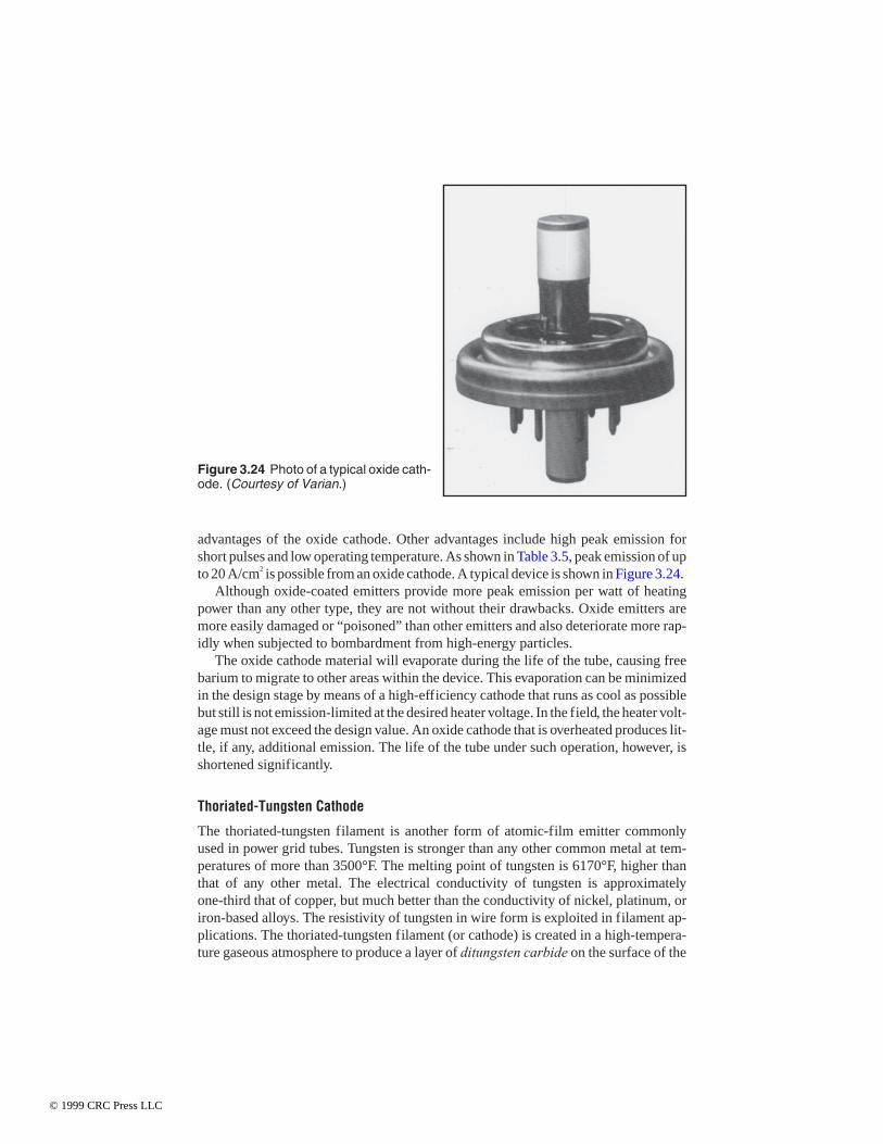
advantages of the oxide cathode. Other advantages include high peak emission forshort pulses and low operating temperature. As shown in Table 3.5, peak emission of upto 20 A/cm2 is possible from an oxide cathode. A typical device is shown in Figure 3.24.
Although oxide-coated emitters provide more peak emission per watt of heatingpower than any other type, they are not without their drawbacks. Oxide emitters aremore easily damaged or “poisoned” than other emitters and also deteriorate more rap-idly when subjected to bombardment from high-energy particles.
The oxide cathode material will evaporate during the life of the tube, causing freebarium to migrate to other areas within the device. This evaporation can be minimizedin the design stage by means of a high-efficiency cathode that runs as cool as possiblebut still is not emission-limited at the desired heater voltage. In the field, the heater volt-age must not exceed the design value. An oxide cathode that is overheated produces lit-tle, if any, additional emission. The life of the tube under such operation, however, isshortened significantly.
Thoriated-Tungsten Cathode
The thoriated-tungsten filament is another form of atomic-film emitter commonlyused in power grid tubes. Tungsten is stronger than any other common metal at tem-peratures of more than 3500°F. The melting point of tungsten is 6170°F, higher thanthat of any other metal. The electrical conductivity of tungsten is approximatelyone-third that of copper, but much better than the conductivity of nickel, platinum, oriron-based alloys. The resistivity of tungsten in wire form is exploited in filament ap-plications. The thoriated-tungsten filament (or cathode) is created in a high-tempera-ture gaseous atmosphere to produce a layer of ditungsten carbide on the surface of the
Figure 3.24 Photo of a typical oxide cath-ode. (Courtesy of Varian.)
© 1999 CRC Press LLC

cathode element(s). Thorium is added to tungsten in the process of making tungstenwire. The thorium concentration is typically about 1.5 percent, in the form of thoria.By proper processing during vacuum pumping of the tube envelope, the metallic tho-rium is brought to the surface of the filament wire. The result is an increase in emis-sion of approximately 1000 times over a conventional cathode.
At a typical operating temperature of 1600 to 1800°C, a thoriated-tungsten filamentwill produce an average emission of 40 to 430 mA/cm2. Peak current ranges up to 10A/cm2 or more.
One of the advantages of a thoriated-tungsten cathode over an oxide cathode is theability to operate the plate at higher voltages. Because oxide cathodes are susceptible todeterioration caused by ion bombardment, plate voltage must be limited. Athoriated-tungsten cathode is more tolerant of ion bombardment, so higher plate volt-ages can be safely applied.
The end of useful life for a thoriated-tungsten tube occurs when most of the carbonhas evaporated or has combined with residual gas, depleting the carbide surface layer.Theoretically, a 3 percent increase in filament voltage will result in a 20 degree Kelvin(K) increase in cathode temperature, a 20 percent increase in peak emission, and a 50percent decrease in tube life because of carbon loss. This cycle works in reverse, too.For a small decrease in temperature and peak emission, the life of the carbidelayer—hence, the tube—may be increased.
Tungsten-Impregnated Cathode
The tungsten-impregnated cathode typically operates at 900 to 1175°C and providesthe highest average emission density of the three types of cathodes discussed in thissection (500 mA/cm2 to 8 A/cm2). Peak power performance ranges up to 12 A/cm2.
Tungsten, as an element, is better able than other emitters to withstand bombard-ment by high-energy positive ions without suffering emission impairment. These posi-tive ions are always present in small numbers in vacuum tubes as a result of ionizationby collision with the residual gas.
Cathode Construction
Power tube filaments can be assembled in several different configurations. Figure3.25 shows a spiral-type filament, and Figure 3.26 shows a bar-type design. The spiralfilament is used extensively in low-power tubes. As the size of the tube increases, me-chanical considerations dictate a bar-type filament with spring loading to compensatefor thermal expansion. A mesh filament can be used for both small and large tubes. Itis more rugged than other designs and less subject to damage from shock and vibra-tion. The rigidity of a cylindrical mesh cathode is determined by the following param-eters:
• The diameter of the cathode
• The number, thickness, and length of the wires forming the cathode
• The ratio of welded to total wire crossings
© 1999 CRC Press LLC

A mesh cathode is shown in Figure 3.27.Most power grid tubes are designed as a series of electron gun structures arranged in
a cylinder around a centerline. This construction allows large amounts of plate currentto flow and to be controlled with a minimum of grid interception. With reduced grid in-
Figure 3.25 Spiral-type tungsten filament.(Courtesy of Varian.)
Figure 3.26 Bar-type tungsten filament.(Courtesy of Varian.)
© 1999 CRC Press LLC

terception, less power is dissipated in the grid structures. In the case of the control grid,less driving power is required for the tube.
In certain applications, the construction of the filament assembly may affect the per-formance of the tube, and that of the RF system as a whole. For example, filaments builtin a basket-weave mesh arrangement usually offer lower distortion in critical high-levelAM modulation circuits.
Velocity of Emission
The electrons emitted from a hot cathode depart with a velocity that represents thedifference between the kinetic energy possessed by the electron just before emissionand the energy that must be given up to escape. Because the energy of different elec-trons within the emitter is not the same, the velocity of emission will vary as well,ranging from zero to a maximum value determined by the type and style of emitter.
3.3.3 Grid Structures
The type of grid used for a power tube is determined principally by the power leveland operating frequency required. For most medium-power tubes (5 to 25 kW dissipa-tion) welded-wire construction is common. At higher power levels, laser-cut pyrolyticgraphite grids may be found. The grid structures of a power tube must maintain theirshape and spacing at elevated temperatures. They also must withstand shock and vi-bration.
Figure 3.27 Mesh tungsten filament.(Courtesy of Varian.)
© 1999 CRC Press LLC

Wire Grids
Conventional wire grids are prepared by operators that wind the assemblies using spe-cial mandrels (forms) that include the required outline of the finished grid. The opera-tors spot weld the wires at intersecting points, as shown in Figure 3.28. Most grids ofthis type are made with tungsten or molybdenum, which exhibit stable physical prop-erties at elevated temperatures. On a strength basis, pure molybdenum generally isconsidered the most suitable of all refractory metals at temperatures of 1600 to3000°F. The thermal conductivity of molybdenum is more than three times that ofiron and almost half that of copper.
Grids for higher-power tubes typically are built using a bar-cage type of construc-tion. A number of vertical supports are fastened to a metal ring at the top and to a basecone at the bottom. The lower end of the assembly is bonded to a contact ring. The con-struction of the ring, metal base cone, and cylindrical metal base give the assembly lowlead inductance and low RF resistance.
The external loading of a grid during operation and the proximity of the grid to thehot cathode impose severe demands on both the mechanical stability of the structureand the physical characteristics of its surface. The grid absorbs a high proportion of theheat radiated by the cathode. It also intercepts the electron beam, converting part of itskinetic energy into heat. Furthermore, high-frequency capacitive currents flowing inthe grid create additional heat.
The result is that grids are forced to work at temperatures as high as 1500°C. Theirprimary and secondary emissions, however, must be low. To prevent grid emission,high electron affinity must be ensured throughout the life of the tube, even though it is
Figure 3.28 Mesh grid structure. (Courtesyof Varian.)
© 1999 CRC Press LLC

impossible to prevent material that evaporates from the cathode from contaminatingthe grid surface.
In tubes with oxide cathodes, grids made of tungsten or molybdenum wire arecoated with gold to reduce primary emission caused by deposition. The maximum safeoperating temperature for gold plating, however, is limited (about 550°C). Specialcoatings developed for high-temperature applications are effective in reducing gridemission. In tubes with thoriated-tungsten cathodes, grids made of tungsten or molyb-denum are coated with proprietary compounds to reduce primary emission.
Primary grid emission is usually low in a thoriated tungsten cathode device. In thecase of an oxide cathode, however, free barium may evaporate from the cathode coatingmaterial and find its way to the control and screen grids. The rate of evaporation is afunction of cathode temperature and time. A grid contaminated with barium will be-come another emitting surface. The hotter the grid, the greater the emissions.
K-Grid
To permit operation at higher powers (and, therefore, higher temperatures) the K-gridhas been developed (Philips). The K-grid is a spot-welded structure of molybdenumwire doped to prevent brittleness and recrystallization. To eliminate mechanicalstresses, the grid is annealed at 1800 K. It is then baked under vacuum at 2300 K todegas the molybdenum wire. The grid structure next is coated with zirconium carbide(sintered at 2300 K) and, finally, with a thin layer of platinum.
Despite high grid temperatures, the platinum coating keeps primary emissions to aminimum. The surface structure maintains low secondary emissions.
Pyrolytic Grid
Pyrolytic grids are a high-performance alternative to wire or bar grid assemblies.Used primarily for high-power devices, pyrolytic grids are formed by laser-cutting agraphite cup of the proper dimensions. The computer-controlled laser cuts numerousholes in the cup to simulate a conventional-style grid. Figure 3.29 shows a typicalpyrolytic-type grid before and after laser processing.
Pyrolytic (or oriented) graphite is a form of crystallized carbon produced by the de-composition of a hydrocarbon gas at high temperatures in a controlled environment. Alayer of pyrolytic graphite is deposited on a grid form. The thickness of the layer is pro-portional to the amount of time deposition is allowed to continue. The structural andmechanical properties of the deposited graphite depend upon the imposed conditions.
Pyrolytic grids are ideal vacuum tube elements because they do not expand likemetal. Their small coefficient of expansion prevents movement of the grids inside thetube at elevated temperatures. This preserves the desired electrical characteristics ofthe device. Because tighter tolerances can be maintained, pyrolytic grids can be spacedmore closely than conventional wire grids. Additional benefits are that the grid:
• Is a single structure having no weld points
• Has a thermal conductivity in two of the three planes nearly that of copper
© 1999 CRC Press LLC

• Can operate at high temperatures with low vapor pressure
Grid Physical Structure
The control, screen, and suppressor grids are cylindrical and concentric. Each isslightly larger than the previous grid, as viewed from the cathode. Each is fastened toa metal base cone, the lower end of which is bonded to a contact ring. Figure 3.30shows the construction of a typical screen grid assembly. Figure 3.31 provides acutaway view of a tetrode power tube.
The shape of the control grid and its spacing from the cathode define, in large part,the operating characteristics of the tube. For best performance, the grid must be essen-tially transparent to the electron path from the cathode to the plate. In a tetrode, the con-trol and screen grids must be precisely aligned to minimize grid current. For pentodetubes, these two conventions apply, in addition to the requirement for precise alignmentand minimum beam interception for the suppressor grid.
Secondary Emission Considerations
The relationship of the properties of secondary electrons to the grid structures andother elements of a vacuum tube must be considered carefully in any design. As the
Figure 3.29 Pyrolytic graphite grid: (a) before laser processing, (b) completed assem-bly. (Courtesy of Varian.)
(a) (b)
© 1999 CRC Press LLC

power capability of a tube increases, the physical size of the elements also increases.This raises the potential for secondary emission from the control, screen, and sup-pressor grids. Secondary emission may occur regardless of the type of cathode used.
Figure 3.30 The screen grid assembly of a typical tetrode PA tube.
Figure 3.31 The internal arrangement of the anode, screen, control grid, and cathodeassemblies of a tetrode power tube.
© 1999 CRC Press LLC

The yield of secondary electrons may be reduced through the application of surfacetreatments.
In a tetrode, the screen is operated at a relatively low potential, necessary to acceler-ate the electrons emitted from the cathode. Not all electrons pass through the screen ontheir way to the plate. Some are intercepted by the screen grid. As the electrons strikethe screen, other low-energy electrons are emitted. If these electrons have a stronger at-traction to the screen, they will fall back to that element. If, however, they pass into theregion between the screen and the plate, the much higher anode potential will attractthem. The result is electron flow from screen to plate.
Because of the physical construction of a tetrode, the control grid will have virtuallyno control over screen-to-plate current flow as a result of secondary electrons. During aportion of the operating cycle of the device, it is possible that more electrons will leavethe screen grid than will arrive. The result will be a reverse electron flow on the screenelement, a condition common to high-power tetrodes. A low-impedance path for re-verse electron flow must be provided.
Tube manufacturers typically specify the recommended value of bleeding currentfrom the screen power supply to counteract the emission current. Two common ap-proaches are illustrated in Figures 3.32 and 3.33. If the screen power supply impedanceis excessively high in the direction of reverse electron flow, the screen voltage will at-tempt to rise to the plate voltage. Note the emphasis on low impedance in the reverseelectron flow direction. Most regulated power supplies are low impedance in the for-ward electron flow direction only. If the supply is not well bled, the reverse electronswill try to flow from anode to cathode in the regulator series pass element. As the screenvoltage rises, the secondary and plate currents will increase, and the tube will enter arunaway condition.
Figure 3.32 Circuit for providing a low-impedance screen supply for a tetrode.
© 1999 CRC Press LLC

As shown in Figure 3.33, the addition of a 12.5 kΩ resistor from screen to groundprovides a path for screen grid emission (20 mA for the circuit shown). In the circuit ofFigure 3.33, plate current flows through the screen power supply, swamping the screensupply. The screen power supply must, obviously, carry the normal screen and platecurrents. This scheme is used extensively in circuits where the screen is operated at dcground potential. The plate-to-cathode voltage is then the sum of the Eb and Ec2 powersupplies.
The suppressor grid of a pentode lessens the effects of secondary emission in the de-vice, reducing the requirement to provide a reverse electron flow path for the screengrid power supply. The screen current requirement for a pentode, however, may besomewhat higher than for a tetrode of the same general characteristics.
The designer also must consider the impedance of the control grid circuit. Primarygrid emission can result in operational problems if the grid circuit impedance is exces-sively high. Primary grid emission, in the case of an oxide cathode tube, will increasewith tube life.
The size and power of gridded tubes dictate certain characteristics of electrical po-tential. As this geometry increases in electrical terms, significant secondary emissionfrom the control grid can occur. Control grid secondary emission can exist whether thecathode is a thoriated-tungsten or oxide emitter, and it can occur in a triode, tetrode, orpentode. A typical curve of grid current as a function of grid voltage for a high-powerthoriated-tungsten filament tetrode is shown in Figure 3.34. As shown in the figure,grid current decreases and eventually takes a reverse direction as the grid voltage in-creases. This reduction and reversal of grid current can be explained by the normal sec-ondary emission characteristics of the metals used in the grid structure.
The secondary emission characteristics of common metals are presented in curveform in Figure 3.35. The ratio of secondary-to-primary electron current is given as afunction of primary electron potential. An examination of the chart will show the re-gion between 200 and 600 V to be rather critical as far as secondary emission is con-
Figure 3.33 Series power supply configuration for swamping the screen circuit of atetrode.
© 1999 CRC Press LLC

cerned. Any power grid tube that normally operates with 200 to 600 V on the grid canexhibit the negative resistance characteristic of decreasing grid current with increasinggrid voltage when another electrode—such as the anode in a triode or the screen grid ina tetrode—is at a sufficiently high potential to attract the emitted electrons from thecontrol grid. A driver stage that works into such a nonlinear load normally must be de-
Figure 3.34 Typical curve of grid current as a function of control grid voltage for ahigh-power thoriated-tungsten filament tetrode.
Figure 3.35 Secondary emission characteristics of various metals under ordinary con-ditions.
© 1999 CRC Press LLC

signed in such a manner as to tolerate this condition. One technique involves swampingthe driver so that changes in the load resulting from secondary grid emission representonly a small percentage of the total load the driver works into.
3.3.4 Plate Assembly
The plate assembly of a power tube is typically a collection of many smaller parts thatare machined and assembled to tight specifications. Copper generally is used to con-struct the anode. It is an excellent material for this purpose because it has the highestelectrical conductivity of any metal except pure silver. Furthermore, copper is easilyfabricated and ideally suited to cold-forming operations such as deep drawing, bend-ing, and stamping.
The anode and cooling fins (in the case of an air-cooled device) begin as flat sheetsof copper. They are stamped by the tube manufacturer into the necessary sizes andshapes. After all of the parts have been machined, the anode and cooling fins arestacked in their proper positions, clamped, and brazed into one piece in a brazing fur-nace.
The plate of a power tube resembles a copper cup with the upper half of a plate con-tact ring welded to the mouth and cooling fins silver-soldered or welded to the outsideof the assembly. The lower half of the anode contact ring is bonded to a base ceramicspacer. At the time of assembly, the two halves of the ring are welded together to form acomplete unit, as shown in Figure 3.36.
In most power tubes, the anode is a part of the envelope and, because the outer sur-face is external to the vacuum, it can be cooled directly. Glass envelopes were used inolder power tubes. Most have been replaced, however, with devices that use ceramic asthe envelope material.
3.3.5 Ceramic Elements
Ceramics are an integral part of modern power vacuum tubes. Three types of ceramicsare in common usage in the production of vacuum devices:
• Aluminum oxide-based ceramics
• Beryllium oxide (BeO)-based ceramics
• Aluminum nitride (AlNi)-based ceramics
Aluminum Oxide Ceramics
Aluminum oxide-based ceramic insulators are a common construction material for awide variety of electric components, including vacuum tubes. Aluminum oxide is 20times higher in thermal conductivity than most oxides. The flexure strength of com-mercial high-alumina ceramics is two to four times greater than that of most oxide ce-ramics. There are drawbacks, however, to the use of alumina ceramics, including:
© 1999 CRC Press LLC

• Relatively high thermal expansion (approximately 7 ppm/°C), compared to otherceramic materials, such as BeO
• Moderately high dielectric constant (approximately 10)
Aluminas are fabricated from aluminum oxide powders with various percentages ofsintering promoters, which produce the glassy phase. The later additives reduce thedensification temperatures to between 1500 and 1600°C. Based on the final applica-tion, the powders may be pressed, extruded, or prepared in slurries for slip casting ortape casting. The surface finish of aluminas is typically 3 to 25 µm/in as a result of nor-mal processing. For very smooth finishes (2 µm/in), the surfaces may be lapped or pol-ished.
Alumina ceramics for vacuum tube applications rarely are used apart from beingbonded to metals. The means by which this is accomplished frequently dictate the pro-cessing technique. Metallization of aluminas usually is accomplished by eitherhigh-temperature firing or low-temperature thick-film processing. Fired, shapedaluminas usually are postmetallized by refiring the formed article after it has beencoated with a slurry of molybdenum and manganese powder or tungsten metal powder.Based on the purity of the alumina, glass powder may be added to the metal powder.The mechanism of metallization requires an internal glassy phase or the added glassyphase for proper bonding. This is accomplished by firing in slightly reducing and moistatmospheres at temperatures above 1500°C. The resulting metallization usually isplated electrochemically with nickel, copper, or both.
Figure 3.36 A cutaway view of the anode structure of an RF power amplifier tube.
© 1999 CRC Press LLC

Thick-film processing of alumina ceramics traditionally has been performed in oxi-dizing atmospheres at moderate temperatures (800 to 1000°C). Precious metals areused, such as gold, silver, platinum, palladium, and their combinations. A glassy phaseusually is incorporated in the thick-film paste.
Each approach to metallization has advantages and disadvantages. The advantage ofthe high-temperature metallization schemes with molybdenum or tungsten is theirmoderate cost. The disadvantage is the high resistivity of the resulting films. These at-tributes are reversed for thick-film materials. Another advantage of thick-filmmetallization is that the process often is applied by the device fabricator, not the ce-ramic vendor. This can allow for greater efficiency in design modification.
In tubes designed for operation at 100 MHz and below, alumina typically is the ce-ramic of choice.
Beryllium Oxide Ceramics
Beryllium oxide-based ceramics are in many ways superior to alumina-based ceram-ics. The major drawback is the toxicity of BeO. Beryllium and its compounds are agroup of materials that are potentially hazardous and must be handled properly. Withthe necessary safeguards, BeO has been used successfully in many tube designs.
Beryllium oxide materials are particularly attractive for use in power vacuum tubesbecause of their electrical, physical, and chemical properties. The thermal conductivityof BeO is approximately 10 times higher than that of alumina-based materials. Figure3.37 compares the thermal conductivity of BeO with that of alumina and some alterna-tive materials. As the chart illustrates, BeO has a lower dielectric constant and coeffi-cient of thermal expansion than alumina. It is, however, also slightly lower in strength.
Figure 3.37 Thermal conductivity of common ceramics.
© 1999 CRC Press LLC

Beryllia materials are fabricated in much the same way as alumina compounds, al-though the toxic properties of the powders mandate that they be processed in laborato-ries equipped to handle them safely. Simple cutting, drilling, and postmetallization alsoare handled by vendors with special equipment. Reliable thick-film systems may be ap-plied to BeO substrates. Such coatings usually necessitate less elaborate safety precau-tions and are often applied by the device fabricator. General safety precautions relatingto BeO ceramics are given in Section 11.3.2.
Other Ceramics
Aluminum nitride (AlNi)-based ceramics have been developed as an alternative to thetoxicity concerns of BeO-based materials. As shown in Figure 3.37, the thermal con-ductivity of AlNi is comparable to that of BeO but deteriorates less with temperature.The dielectric constant of AlNi is comparable to that of alumina (a drawback), but itsthermal expansion is low (4 ppm/°C).
Other ceramic materials that find some use in vacuum devices include silicon car-bide (SiC)-based substances and boron nitride ceramics.
3.3.6 Tube Construction
Each type of power grid tube is unique insofar as its operating characteristics are con-cerned. The basic physical construction, however, is common to most devices. A vac-uum tube is built in essentially two parts:
• The base, which includes the filament and supporting stem, control grid, screengrid, and suppressor grid (if used)
• The anode, which includes the heat-dissipating fins made in various machiningsteps
The base subassembly is welded using a tungsten-inert gas (TIG) process in an oxy-gen-free atmosphere (a process sometimes referred to as Heliarc welding) to producea finished base unit.
The ceramic elements used in a vacuum tube are critical parts of the device. Assem-bled in sections, each element builds upon the previous one to form the base of the tube.The ceramic-to-metal seals are created using a material that is painted onto the ceramicand then heated in a brazing oven. After preparation in a high-temperature oven, thepainted area provides a metallic structure that is molecularly bonded to the ceramic andprovides a surface suitable for brazing.
This process requires temperature sequences that dictate completion of the high-est-temperature stages first. As the assembly takes form, lower oven temperatures areused so that completed bonds will not be compromised.
Despite all the advantages that make ceramics one of the best insulators for a tubeenvelope, their brittleness is a potential cause of failure. The smallest cracks in the ce-ramic, not in themselves damaging, can cause the ceramic to break when mechanicallystressed by temperature changes.
© 1999 CRC Press LLC

After the base assembly has been matched with the anode, the completed tube isbrazed into a single unit. The device then goes through a bake-out procedure. Bakingstations are used to evacuate the tube and bake out any oxygen or other gases from thecopper parts of the assembly. Although oxygen-free copper is used in tube construc-tion, some residual oxygen exists in the metal and must be driven out for long compo-nent life. A typical vacuum reading of 10-8 Torr is specified for most power tubes (for-merly expressed as 10-8 mm of mercury). For comparison, this is the degree of vacuumin outer space about 200 miles above the earth.
A vacuum offers excellent electrical insulation characteristics. This property is es-sential for reliable operation of a vacuum tube, the elements of which typically operateat high potentials with respect to each other and to the surrounding environment. Anelectrode containing absorbed gases, however, will exhibit reduced breakdown voltagebecause the gas will form on the electrode surface, increasing the surface gas pressureand lowering the breakdown voltage in the vicinity of the gas pocket.
To maintain a high vacuum during the life of the component, power tubes contain agetter device. The name comes from the function of the element: to “get” or trap andhold gases that may exist inside the tube. Materials used for getters include zirconium,cerium, barium, and titanium.
The operation of a vacuum tube is an evolving chemical process. End of life in a vac-uum tube generally is caused by loss of emission.
3.3.7 Connection Points
The high power levels and frequencies at which vacuum tubes operate place stringentdemands on the connectors used to tie the outside world to the inside elements. Tubesare designed to be mounted vertically on their electrical connectors. The connectorsprovide a broad contact surface and mechanical support for the device.
The cathode and grids typically are mounted on ring-shaped Kovar bases, whichalso serve as contact rings for the external connections. Kovar is an iron-nickel-cobaltalloy whose coefficient of thermal expansion is comparable to that of aluminum oxideceramic. The different diameters of the various contact rings allow them to be groupedcoaxially. The concentric tube/connector design provides for operation at high frequen-cies. Conductivity is improved by silver plating.
3.3.8 Tube Sockets
Any one tube design may have several possible socket configurations, dependingupon the frequency of operation. If the tube terminals are large cylindrical surfaces,the contacting portions of the socket consist of either spring collets or an assembly ofspring fingerstock. Usually, these multiple-contacting surfaces are made of berylliumcopper to preserve spring tension at the high temperatures present at the tube termi-nals. The fingers are silver-plated to reduce RF resistance. Figure 3.38 shows acutaway view of the base of a tetrode socket.
If the connecting fingers of a power tube socket fail to provide adequate contact withthe tube element rings, a concentration of RF currents will result. Depending on the ex-
© 1999 CRC Press LLC

tent of this concentration, damage may result to the socket. After a connecting fingerloses its spring action, the heating effect is aggravated, and tube damage is possible.
A series of specialized power tubes is available with no sockets at all. Intended forcathode-driven service, the grid assembly is formed into a flange that is bolted to thechassis. The filament leads are connected via studs on the bottom of the tube. Such aconfiguration eliminates the requirement for a socket. This type of device is useful forlow-frequency applications, such as induction heating.
3.4 NeutralizationAn RF power amplifier must be properly neutralized to provide acceptable perfor-mance in most applications. The means to accomplish this end vary considerablyfrom one design to another. An RF amplifier is neutralized when two operating condi-tions are met:
• The interelectrode capacitance between the input and output circuits is canceled.
• The inductance of the screen grid and cathode assemblies (in a tetrode) is can-celed.
Cancellation of these common forms of coupling between the input and output cir-cuits of vacuum tube amplifiers prevents self-oscillation and the generation of spuri-ous products.
Figure 3.38 Cross section of the base of a tetrode socket showing the connectionpoints.
© 1999 CRC Press LLC

3.4.1 Circuit Analysis
Figure 3.39 illustrates the primary elements that affect neutralization of a vacuumtube RF amplifier operating in the VHF band. (Many of the following principles alsoapply to lower frequencies.) The feedback elements include the residual grid-to-platecapacitance (Cgp), plate-to-screen capacitance (Cps), and screen grid lead inductance(Ls). The RF energy developed in the plate circuit (Ep) causes a current (I) to flowthrough the plate-to-screen capacitance and the screen lead inductance. The currentthrough the screen inductance develops a voltage (–E) with a polarity opposite that ofthe plate voltage (Ep). The –E potential often is used as a method of neutralizingtetrode and pentode tubes operating in the VHF band.
Figure 3.40 graphically illustrates the electrical properties at work. The circuit ele-ments of the previous figure have been arranged so that the height above or below thezero potential line represents the magnitude and polarity of the RF voltage for each partof the circuit with respect to ground (zero). For the purposes of this illustration, assumethat all of the circuit elements involved are pure reactances. The voltages representedby each, therefore, are either in phase or out of phase and can be treated as positive ornegative with respect to each other.
The voltages plotted in the figure represent those generated as a result of the RF out-put circuit voltage (Ep). No attempt is made to illustrate the typical driving current onthe grid of the tube. The plate (P) has a high positive potential above the zero line, estab-lished at the ground point. Keep in mind that the distance above the baseline representsincreasing positive potential. The effect of the out-of-phase screen potential developedas a result of inductance Ls is shown, resulting in the generation of –E.
Figure 3.39 The elements involved in the neutralization of a tetrode PA stage.
© 1999 CRC Press LLC

As depicted, the figure constitutes a perfectly neutralized circuit. The grid potentialrests at the zero baseline. The grid operates at filament potential insofar as any action ofthe output circuit on the input circuit is concerned.
The total RF voltage between plate and screen is made up of the plate potential andscreen lead inductance voltage, –E. This total voltage is applied across a divider circuitthat consists of the grid-to-plate capacitance and grid-to-screen capacitance (Cgp andCgs). When this potential divider is properly matched for the values of plate RF voltage(Ep) and screen lead inductance voltage (–E), the control grid will exhibit zero voltagedifference with respect to the filament as a result of Ep.
3.4.2 Circuit Design
A variety of methods may be used to neutralize a vacuum tube amplifier. Generallyspeaking, a grounded-grid, cathode-driven triode can be operated into the VHF bandwithout external neutralization components. The grounded-grid element is sufficientto prevent spurious oscillations. Tetrode amplifiers generally will operate through theMF band without neutralization. However, as the gain of the stage increases, the needto cancel feedback voltages caused by tube interelectrode capacitances and externalconnection inductances becomes more important. At VHF and above, it is generallynecessary to provide some form of stage neutralization.
Below VHF
For operation at frequencies below the VHF band, neutralization for a tetrode typi-cally employs a capacitance bridge circuit to balance out the RF feedback caused by
Figure 3.40 A graphical representation of the elements involved in theself-neutralization of a tetrode RF stage.
© 1999 CRC Press LLC

residual plate-to-grid capacitance. This method assumes that the screen is well by-passed to ground, providing the expected screening action inside the tube.
Neutralization of low-power push-pull tetrode or pentode tubes can be accom-plished with cross-neutralization of the devices, as shown in Figure 3.41. Small-valueneutralization capacitors are used. In some cases, neutralization can be accomplishedwith a simple wire connected to each side of the grid circuit and brought through thechassis deck. Each wire is positioned to “look at” the plate of the tube on the oppositehalf of the circuit. Typically, the wire (or a short rod) is spaced a short distance from theplate of each tube. Fine adjustment is accomplished by moving the conductor in or outfrom its respective tube.
A similar method of neutralization can be used for a cathode-driven symmetricalstage, as shown in Figure 3.42. Note that the neutralization capacitors (Cn) are con-nected from the cathode of one tube to the plate of the opposite tube. The neutralizingcapacitors have a value equal to the internal cathode-to-plate capacitance of the PAtubes.
In the case of a single-ended amplifier, neutralization can be accomplished using ei-ther a push-pull output or push-pull input circuit. Figure 3.43 shows a basic push-pullgrid neutralization scheme that provides the out-of-phase voltage necessary for properneutralization. It is usually simpler to create a push-pull network in the grid circuit thanin the plate because of the lower voltages present. The neutralizing capacitor, Cn, issmall and may consist of a simple feedthrough wire (described previously). A paddingcapacitor in parallel with C1 often is added to maintain the balance of the input circuitwhile tuning. The padding capacitor generally is equal in size to the input capacitanceof the tube.
Single-ended tetrode and pentode stages also can be neutralized using the methodshown in Figure 3.44. The input resonant circuit is placed above ground by a smallamount because of the addition of capacitor C. The voltage to ground that develops
Figure 3.41 Push-pull grid neutralization.
© 1999 CRC Press LLC

across C upon the application of RF drive is out of phase with the grid voltage, and is fedback to the plate through Cn to provide neutralization. In such a design, Cn is consider-ably larger in value than the grid-to-plate interelectrode capacitance.
The single-ended grid neutralization circuit is redrawn in Figure 3.45 to show the ca-pacitance bridge that makes the design work. Balance is obtained when the followingcondition is met:
C
C
C
Cn gp
gf
= (3.12)
Figure 3.43 Push-pull grid neutralization in a single-ended tetrode stage.
Figure 3.42 Symmetrical stage neutralization for a grounded-grid circuit.
© 1999 CRC Press LLC

Where:Cn = neutralization capacitanceC = input circuit bypass capacitorCgp = grid-to-plate interelectrode capacitanceCgf = total input capacitance, including tube and stray capacitance
A single-ended amplifier also can be neutralized by taking the plate circuit slightlyabove ground and using the tube capacitances as part of the neutralizing bridge. Thiscircuit differs from the usual RF amplifier design in that the plate bypass capacitor is re-turned to the screen side of the screen bypass capacitor, as shown in Figure 3.46. Thesize of screen bypass capacitor Cs and the amount of stray capacitances in Cp are chosen
Figure 3.44 Single-ended grid neutralization for a tetrode.
Figure 3.45 The previous figure redrawn to show the elements involved in neutraliza-tion.
© 1999 CRC Press LLC

to balance the voltages induced in the input by the internal tube capacitances,grid-to-plate (Cgp) and screen-to-grid (Csg). This circuit is redrawn in Figure 3.47 in theusual bridge form. Balance is obtained when the following condition is met:
C
C
C
C
p
s
gp
sg
= (3.13)
In usual tetrode and pentode structures, the screen-to-grid capacitance is approxi-mately half the published tube input capacitance. The tube input capacitance is primar-ily the sum of the grid-to-screen capacitance and the grid-to-cathode capacitance.
Note that in the examples given, it is assumed that the frequency of operation is lowenough that inductances in the socket and connecting leads can be ignored. This is basi-
Figure 3.46 Single-ended plate neutralization.
Figure 3.47 Single-ended plate neutralization showing the capacitance bridge present.
© 1999 CRC Press LLC

cally true in MF applications and below. At higher bands, however, the effects of strayinductances must be considered, especially in single-ended tetrode and pentode stages.
VHF and Above
Neutralization of power grid tubes operating at very high frequencies provides specialchallenges and opportunities to the design engineer. At VHF and above, significantRF voltages may develop in the residual inductance of the screen, grid, and cathodeelements. If managed properly, these inductances can be used to accomplish neutral-ization in a simple, straightforward manner.
At VHF and above, neutralization is required to make the tube input and output cir-cuits independent of each other with respect to reactive currents. Isolation is necessaryto ensure independent tuning of the input and output. If variations in the output voltageof the stage produce variations of phase angle of the input impedance, phase modula-tion will result.
As noted previously, a circuit exhibiting independence between the input and outputcircuits is only half of the equation required for proper operation at radio frequencies.The effects of incidental inductance of the control grid also must be canceled for com-plete stability. This condition is required because the suppression of coupling by capac-itive currents between the input and output circuits is not, by itself, sufficient to negatethe effects of the output signal on the cathode-to-grid circuit. Both conditions—inputand output circuit independence and compensation for control grid lead induc-tance—must be met for complete stage stability at VHF and above.
Figure 3.48 shows a PA stage employing stray inductance of the screen grid toachieve neutralization. In this grounded-screen application, the screen is bonded to thecavity deck using six short connecting straps. Two additional adjustable ground strapsare set to achieve neutralization.
3.4.3 Grounded-Grid Amplifier Neutralization
Grounded-grid amplifiers offer an attractive alternative to the more commongrid-driven circuit. The control grid is operated at RF ground and serves as a shield tocapacitive currents from the output to the input circuit. Generally, neutralization is notrequired until the control grid lead inductive reactance becomes significant. The feed-back from the output to the input circuit is no longer the result of plate-to-filament ca-pacitance. The physical size of the tube and the operating frequency determine whenneutralization is required.
Two methods of neutralization commonly are used with grounded-grid amplifiers.In the first technique, the grids of a push-pull amplifier are connected to a point havingzero impedance to ground, and a bridge of neutralizing capacitances is used that isequal to the plate-filament capacitances of the tubes.
The second method of neutralization requires an inductance between the grid andground, or between the grids of a push-pull amplifier, of a value that will compensatefor the coupling between input and output circuits resulting from the internal capaci-tances of the tubes.
© 1999 CRC Press LLC

Behavior of these two circuits is quite different. They may be considered as specialforms of the more general case in which the neutralizing capacitors have values differ-ing from the internal capacitances of the tubes, and in which an appropriate reactance isconnected between the grids. Under these conditions, the value of neutralizing capaci-
Figure 3.48 A grounded-screen PA stage neutralized through the use of stray induc-tance between the screen connector and the cavity deck: (a) schematic diagram, (b)mechanical layout of cavity.
(a)
(b)
© 1999 CRC Press LLC

tance permits continuous variation of power amplification, stability, and negative feed-back.
Grid Impedance
In the special case of a grounded-grid amplifier having a grid impedance and the re-active currents neutralized, the following equations apply (see Figure 3.49):
C CC
n fp
fg= −µ
(3.14)
( )Z
j C Cg
fg gp
= −+ +
1
1ω µ(3.15)
If in solving the equation for Cn the sign is negative, this indicates that in-phase neu-tralization is required. Conversely, if the sign of Cn is positive, then out-of-phase neu-tralization is needed. A negative value of Zg indicates capacitive reactance required,and a positive value indicates that inductive reactance is to be used.
Application Example
If the grids of a push-pull cathode-driven amplifier are not at ground potential be-cause the inductance of the leads is not negligible, coupling may exist between the in-put and output circuits through the plate-grid capacitances, cathode-grid capaci-tances, and grid-to-grid inductance. One method of reducing this coupling is to insertbetween the grids a series-tuned circuit that has zero reactance at the operating fre-quency. This technique is illustrated in Figure 3.50. This neutralization scheme is use-
Figure 3.49 Circuit of grounded-grid amplifier having grid impedance and neutralizedfor reactive currents.
© 1999 CRC Press LLC

ful only for the case in which no grid current flows. If grid current flows, a grid resis-tance will appear in parallel with the grid-to-filament capacitance. If the resistance issmall in comparison with the reactance of this grid-to-filament capacitance, phasemodulation will result.
Another important property of the preceding neutralization scheme is that poweramplification is a function of the neutralizing capacitance, while the independence ofcathode and plate circuits from the viewpoint of reactive currents may be obtained withany value of neutralizing capacitance. If the neutralizing capacitance is less than theplate-to-filament capacitance of the tube, the stage will operate with low excitationpower and high power amplification.
If the neutralizing capacitance is greater than the plate-to-filament capacitance, thepower amplification will be quite low, but the total output power possible will be in-creased.
3.4.4 Self-Neutralizing Frequency
The voltage-dividing action between the plate-to-grid capacitance (Cpg) and thegrid-to-screen capacitance (Cgs) will not change with variations in operating fre-quency. The voltage division between the plate and screen, and screen and groundcaused by the charging current (I) will, however, vary significantly with frequency.There will be a particular frequency, therefore, at which this potential-dividing circuit
Figure 3.50 Neutralization by cross-connected capacitors of a symmetrical cath-ode-excited amplifier wth compensation of lead inductance.
© 1999 CRC Press LLC

will effectively place the grid at filament potential insofar as the plate is concerned.This point is known as the self-neutralizing frequency, illustrated in Figure 3.51.
At the self-neutralizing frequency, the tetrode or pentode is inherently neutralizedby the circuit elements within the device itself, and external screen inductance toground. When a device is operated below its self-neutralizing frequency, the normalcross-neutralization circuits apply. When the operating frequency is above the self-neu-tralizing frequency, the voltage developed in the screen lead inductance is too large togive the proper voltage division between the internal capacitances of the device. Oneapproach to neutralization in this case involves adjusting the inductive reactance of thescreen lead to ground to lower the total reactance. In the example shown in Figure 3.52,this is accomplished with a series variable capacitor.
Another approach is shown in Figure 3.53, in which the potential divider networkmade up of the tube capacitance is changed. In the example, additional plate-to-grid ca-pacitance is added external to the tube. The external capacitance (Cext) can take the formof a small wire or rod positioned adjacent to the plate of the tube. This approach is simi-lar to the one described in Section 3.4.2, except that in this case the neutralizing probe isconnected to the grid of the tube, rather than to an opposite polarity in the circuit.
If the RF power amplifier is operating above the self-neutralizing frequency of thetube and must be tuned over a range of frequencies, it is probably easier to use thescreen series-tuning capacitor method and make this control available to the operator. Ifoperation is desired over a range of frequencies including the self-neutralizing fre-quency of the tube, this circuit is also desirable because the incidental lead inductancein the variable capacitor lowers the self-neutralizing frequency of the circuit so that theneutralizing series capacitor can be made to operate over the total desired frequencyrange. If this range is too great, switching of neutralizing circuits will be required. Asmall 50 to 100 pF variable capacitor in the screen lead often has been found to be satis-factory.
Figure 3.51 Graphical representation of the elements of a tetrode whenself-neutralized.
© 1999 CRC Press LLC

Another method of changing the self-neutralizing frequency of a tetrode or pentodecan be fashioned from the general bypassing arrangement of the screen and filamentshown in Figure 3.54. The screen lead is bypassed with minimum inductance to the fil-ament terminal of the tube. Some inductance is introduced in the common filament andscreen ground leads. The grid is shown below the zero voltage or chassis potential, indi-cating that the voltage developed in the screen lead inductance to chassis is excessive. Ifthe filament is tapped on this inductance, a point can be found where the voltage differ-
Figure 3.52 Components of the output voltage of a tetrode when neutralized by addingseries screen-lead capacitance.
Figure 3.53 Components of the output voltage of a tetrode when neutralized by addingexternal grid-to-plate capacitance.
© 1999 CRC Press LLC

ence between the grid and filament is zero, as far as the components of plate voltage areconcerned. This arrangement will be found to self-neutralize at a higher frequency thanif the filament and screen were bypassed separately to the chassis. Thus, increasing theself-neutralizing frequency of the tube and screen bypass arrangement reduces the ten-dency of the VHF parasitic to occur.
If the frequency of the VHF parasitic is reduced by increasing the inductance of theplate lead (presuming this is the principal frequency-defining circuit), the circuit can bemade to approach the self-neutralizing frequency of the tube and, therefore, suppressthe parasitic.
3.4.5 Neutralization Adjustment
Most neutralization circuits must be adjusted for operation at a given frequency. Theexact procedure followed to make these adjustments varies from one circuit to thenext. The following generalizations, however, apply to most systems.
The first step in the process of neutralization is to break the dc connections to theplate voltage and screen voltage supplies, leaving the RF circuits intact. If the directcurrent path is not broken, some current can flow in either of these circuits even thoughthe voltages are zero. The presence of this current causes the amplifier to work in thenormal manner, generating RF power in the plate circuit. It would then be incorrect toadjust for zero power in the plate circuit. Sufficient RF grid drive must be applied toprovide some grid current or to cause a sensitive RF meter coupled to the plate to givean indication of feedthrough power. When the plate circuit is tuned through resonance,the grid current will dip when the circuit is out of neutralization, or the RF meter willpeak. The neutralization adjustments are made until the indication is minimum.
Another powerful tool for roughly neutralizing an RF amplifier is to feed the poweroutput from a signal generator into the grid circuit. A sensitive RF detector is inserted
Figure 3.54 Components of the output voltage of a tetrode neutralized by adding induc-tance common to the screen and cathode return.
© 1999 CRC Press LLC

between the output connector and the load. Neutralization can then be adjusted for min-imum feedthrough. This technique is useful in working with prototype equipment. Ac-tual qualitative measurements can be made. If the insertion loss of the amplifier is lessthan the expected gain, oscillation will occur. Circuit modifications can be made untilthe isolation is sufficient to warrant a test with high voltages applied. The advantages ofthis “cold” system test are that:
• No components are subjected to unusual stress if the amplifier is unstable.
• Circuit adjustments can be made safely because no high voltages are present.
For final trimming of the neutralization adjustment, the stage should be returned tooperating condition at reduced power (similar to that used when testing for parasitic os-cillations), or under the final loaded operating conditions. At higher frequencies, par-ticularly in the VHF region, it will be found that a small additional trimming adjustmentof the neutralization circuit is usually required. When the plate circuit is tuned throughresonance, minimum plate current and maximum control grid current should occur si-multaneously. In the case of the tetrode and pentode, the dc screen current should bemaximum at the same time.
These neutralizing procedures apply not only to the HF radio frequencies, but also tothe VHF and UHF regions.
3.5 References1. Terman, F. E., Radio Engineering, 3rd Ed., McGraw-Hill, New York, 1947.2 . Ferris, Clifford D., “Electron Tube Fundamentals,” in The Electronics Handbook,
Jerry C. Whitaker (ed.), CRC Press, Boca Raton, FL, pp. 295–305, 1996.
3.6 BibliographyBirdsall, C. K., Plasma Physics via Computer Simulation, Adam Hilger, 1991.Block, R., “CPS Microengineers New Breed of Materials,” Ceramic Ind., pp. 51–53,
April 1988.Buchanan, R. C., Ceramic Materials for Electronics, Marcel Dekker, New York, 1986.“Ceramic Products,” Brush Wellman, Cleveland, OH.Chaffee, E. L., Theory of Thermonic Vacuum Tubes, McGraw-Hill, New York, 1939.“Combat Boron Nitride, Solids, Powders, Coatings,” Carborundum Product Litera-
ture, form A-14, 011, September 1984.“Coors Ceramics—Materials for Tough Jobs,” Coors Data Sheet K.P.G.-2500-2/87
6429.Cote, R. E., and R. J. Bouchard, “Thick Film Technology,” in Electronic Ceramics, L.
M. Levinson (ed.), Marcel Dekker, New York, pp. 307–370, 1988.Dettmer, E. S., and H. K. Charles, Jr., “AlNi and SiC Substrate Properties and Pro-
cessing Characteristics,” Advances in Ceramics, Vol. 31, American Ceramic Soci-ety, Columbus, OH, 1989.
© 1999 CRC Press LLC

Dettmer, E. S., H. K. Charles, Jr., S. J. Mobley, and B. M. Romenesko, “Hybrid Designand Processing Using Aluminum Nitride Substrates,” ISHM 88 Proc., pp. 545–553,1988.
Eastman, Austin V., Fundamentals of Vacuum Tubes, McGraw-Hill, 1941.Fink, D., and D. Christiansen (eds.), Electronics Engineers’ Handbook, 3rd Ed.,
McGraw-Hill, New York, 1989.Floyd, J. R., “How to Tailor High-Alumina Ceramics for Electrical Applications,” Ce-
ramic Ind., pp. 44–47, February 1969; pp. 46–49, March 1969.Gray, Truman S., Applied Electronics, John Wiley & Sons, New York, 1954.Harper, C. A., Electronic Packaging and Interconnection Handbook, McGraw-Hill,
New York, 1991.“High Power Transmitting Tubes for Broadcasting and Research,” Philips Technical
Publication, Eindhoven, the Netherlands, 1988.Iwase, N., and K. Shinozaki, “Aluminum Nitride Substrates Having High Thermal
Conductivity,” Solid State Technol., pp. 135–137, October 1986.Jordan, Edward C., (ed.), Reference Data for Engineers: Radio, Electronics, Computer
and Communications, 7th Ed., Howard W. Sams, Indianapolis, IN, 1985.Kingery, W. D., H. K. Bowen, and D. R. Uhlmann, Introduction to Ceramics, John
Wiley & Sons, New York, pp. 637, 1976.Kohl, Walter, Materials Technology for Electron Tubes, Reinhold, New York.Laboratory Staff, The Care and Feeding of Power Grid Tubes, Varian Eimac, San
Carlos, CA, 1984.Lafferty, J. M., Vacuum Arcs, John Wiley & Sons, New York, 1980.Mattox, D. M., and H. D. Smith, “The Role of Manganese in the Metallization of High
Alumina Ceramics,” J. Am. Ceram. Soc., Vol. 64, pp. 1363–1369, 1985.Mistler, R. E., D. J. Shanefield, and R. B. Runk, “Tape Casting of Ceramics,” in G. Y.
Onoda, Jr., and L. L. Hench (eds.), Ceramic Processing Before Firing, John Wiley& Sons, New York, pp. 411–448, 1978.
Muller, J. J., “Cathode Excited Linear Amplifiers,” Electrical Communications, Vol.23, 1946.
Powers, M. B., “Potential Beryllium Exposure While Processing Beryllia Ceramics forElectronics Applications,” Brush Wellman, Cleveland, OH.
Reich, Herbert J., Theory and Application of Electronic Tubes, McGraw-Hill, NewYork, 1939.
Roth, A., Vacuum Technology, 3rd Ed., Elsevier Science Publishers B. V., 1990.Sawhill, H. T., A. L. Eustice, S. J. Horowitz, J. Gar-El, and A. R. Travis, “Low Temper-
ature Co-Fireable Ceramics with Co-Fired Resistors,” in Proc. Int. Symp. on Micro-electronics, pp. 173–180, 1986.
Schwartz, B., “Ceramic Packaging of Integrated Circuits,” in Electronic Ceramics, L.M. Levinson (ed.), Marcel Dekker, New York, pp. 1–44, 1988.
Strong, C. E., “The Inverted Amplifier,” Electrical Communications, Vol. 19, no. 3,1941.
Whitaker, J. C., Radio Frequency Transmission Systems: Design and Operation,McGraw-Hill, New York, 1991.
© 1999 CRC Press LLC

Whitaker, Jerry C. “Chapter 4 – Designing Vacuum Tube Circuits” Power Vacuum Tubes Handbook 2nd Edition.Ed. Jerry C. WhitakerBoca Raton: CRC Press LLC, 2000
© 1999 CRC Press LLC

Chapter
4Designing Vacuum Tube Circuits
4.1 IntroductionAny number of configurations may be used to generate RF signals using vacuumtubes. Circuit design is dictated primarily by the operating frequency, output power,type of modulation, duty cycle, and available power supply. Tube circuits can be di-vided generally by their operating class and type of modulation employed. As dis-cussed in Section 2.1.4, the angle of plate current flow determines the class of opera-tion:
• Class A = 360° conduction angle
• Class B = 180° conduction angle
• Class C = conduction angle less than 180°
• Class AB = conduction angle between 180 and 360°
The class of operation has nothing to do with whether the amplifier is grid-driven orcathode-driven. A cathode-driven amplifier, for example, can be operated in any de-sired class. The class of operation is only a function of the plate current conductionangle. The efficiency of an amplifier is also a function of the plate current conductionangle.
The efficiency of conversion of dc to RF power is one of the more important charac-teristics of a vacuum tube amplifier circuit. The dc power that is not converted into use-ful output energy is, for the most part, converted to heat. This heat represents wastedpower; the result of low efficiency is increased operating cost for energy. Low effi-ciency also compounds itself. This wasted power must be dissipated, requiring in-creased cooling capacity. The efficiency of the amplifier must, therefore, be carefullyconsidered, consistent with the other requirements of the system. Figure 4.1 shows thetheoretical efficiency attainable with a tuned or resistive load assuming that the peak acplate voltage is equal to the plate supply voltage.
© 1999 CRC Press LLC

4.1.1 Class A Amplifier
A class A amplifier is used in applications requiring low harmonic distortion in theoutput signal. A class A amplifier can be operated with low intermodulation distor-tion in linear RF amplifier service. Typical plate efficiency for a class A amplifier isabout 30 percent. Power gain is high because of the low drive power required. Gainsas high as 30 dB are typical.
4.1.2 Class B and AB Amplifiers
A class AB power amplifier is capable of generating more power—using the sametube—than the class A amplifier, but more intermodulation distortion also will begenerated. A class B RF linear amplifier will generate still more intermodulation dis-tortion, but is acceptable in certain applications. The plate efficiency is typically 66percent, and stage gain is about 20 to 25 dB.
4.1.3 Class C Amplifier
A class C power amplifier is used where large amounts of RF energy need to be gen-erated with high efficiency. Class C RF amplifiers must be used in conjunction withtuned circuits or cavities, which restore the amplified waveform through the flywheeleffect.
The grounded-cathode class C amplifier is the building block of RF technology. It isthe simplest method of amplifying CW, pulsed, and FM signals. The basic configura-tion is shown in Figure 4.2. Tuned input and output circuits are used for impedance
Figure 4.1 Plate efficiency as a function of conduction angle for an amplifier with atuned load.
© 1999 CRC Press LLC

matching and to resonate the stage at the desired operating frequency. The cathode isbypassed to ground using low-value capacitors. Bias is applied to the grid as shown.The bias power supply may be eliminated if a self-bias configuration is used. The typi-cal operating efficiency of a class C stage ranges from 65 to 85 percent.
Figure 4.3 illustrates the application of a zero-bias triode in a grounded-grid ar-rangement. Because the grid operates at RF ground potential, this circuit offers stableperformance without the need for neutralization (at MF and below). The input signal iscoupled to the cathode through a matching network. The output of the triode feeds a pinetwork through a blocking capacitor.
4.2 Principles of RF Power AmplificationIn an RF power amplifier, a varying voltage is applied to the control grid (or cathode,in the case of a grounded-grid circuit) from a driver stage whose output is usually oneof the following:
• Carrier-frequency signal only
• Modulation (intelligence) signal only
• Modulated carrier signal
Simultaneous with the varying control grid signal, the plate voltage will vary in a sim-ilar manner, resulting from the action of the amplified current flowing in the plate cir-cuit. In RF applications with resonant circuits, these voltage changes are smooth sine
Figure 4.2 Basic grounded-cathode RF amplifier circuit.
© 1999 CRC Press LLC

wave variations, 180° out of phase with the input. The relationship is illustrated inFigure 4.4. Note how these variations center about the dc plate voltage and the dc con-trol grid bias. In Figure 4.5, the variations have been indicated next to the plate volt-age and grid voltage scales of a typical constant-current curve. At some instant intime, shown as t on the time scales, the grid voltage has a value denoted eg on the gridvoltage sine wave.
Any point on the operating line (when drawn on constant-current curves as illus-trated in Figure 4.5) tells the instantaneous values of plate current, screen current, andgrid current that must flow when these particular values of grid and plate voltage are ap-plied to the tube. Thus, by plotting the values of plate and grid current as a function oftime t, it is possible to produce a curve of instantaneous values of plate and grid current.Such plots are shown in Figure 4.6.
By analyzing the plate and grid current values, it is possible to predict with accuracythe effect on the plate circuit of a change at the grid. It follows that if a properly loadedresonant circuit is connected to the plate, a certain amount of RF power will be deliv-ered to that circuit. If the resonant circuit is tuned to the fundamental frequency (thesame frequency as the RF grid voltage), the power delivered will be that of the funda-mental or principal RF component of plate current. If the circuit is tuned to a harmonic
Figure 4.3 Typical amplifier circuit using a zero-bias triode. Grid current is measured inthe return lead from ground to the filament.
© 1999 CRC Press LLC

Figure 4.4 Variation of plate voltage as a function of grid voltage.
Figure 4.5 Relationship between grid voltage and plate voltage plotted on a con-stant-current curve.
© 1999 CRC Press LLC

of the grid voltage frequency, the power delivered will be the result of a harmonic com-ponent of the plate current.
4.2.1 Drive Power Requirements
The technical data sheet for a given tube type lists the approximate drive power re-quired for various operating modes. As the frequency of operation increases and thephysical size of the tube structure becomes large with respect to this frequency, thedrive power requirements also will increase.
The drive power requirements of a typical grounded-cathode amplifier consist of sixmajor elements:
• The power consumed by the bias source, given by:
P I Ec c1 1 1= × (4.1)
• The power dissipated in the grid as a result of rectified grid current:
P I ec cmp2 1= × (4.2)
• The power consumed in the tuned grid circuit:
P I Rc rms rf32= ×, (4.3)
• The power lost as a result of transit-time effects:
Pe
Rc rms
t
4
2
=
, (4.4)
Figure 4.6 Instantaneousvalues of plate and grid cur-rent as a function of time.
© 1999 CRC Press LLC

Rt is that part of the resistive component of the tube input impedance resultingfrom transit-time effects, and is given by:
RKg f T
t
m
= 12 2
(4.5)
• The power consumed in that part of the resistive component of the input imped-ance resulting from cathode lead inductance:
Pe
R
g
s
5
2
= (4.6)
Input resistance resulting from the inductance of the cathode leads is foundfrom the following:
Rg L C
s
m k gk
= 12ω
(4.7)
• The power dissipated in the tube envelope because of dielectric loss:
P f E6 12141= . ε (4.8)
Where:Ic1 = dc grid currentEc1 = dc grid voltageEcmp = maximum positive grid voltageIc,rms = rms value of RF grid currentRrf = RF resistance of grid circuitec,rms = rms value of RF grid voltageRt = resistance resulting from transit-time loadingK = a constant (function of the tube geometry)gm = transconductancef = frequency (Hz)T = transit-time, cathode to gridRs = cathode lead inductance input resistance loadingω π= 2 fLk = cathode lead inductance (Henrys)Cgk = grid-to-cathode capacitance (Farads)E1 = voltage gradient (kilovolt per inch, rms)ε = loss factor of dielectric materials
The total drive power Pt is, then, equal to:
P P P P P P Pt = + + + + +1 2 3 4 5 6 (4.9)
© 1999 CRC Press LLC

Particular attention must be given to grid dissipation when a tube is operated in theVHF and UHF regions. The total driving power required for a given output may begreater than the grid dissipation capability of the device.
Operational Considerations for VHF and UHF
For operation of a tube in the VHF and UHF regions, several techniques may be ap-plied to minimize the driving power without appreciably affecting plate conversion ef-ficiency. The most common techniques are:
• Use the minimum dc control bias. Frequently, it is advisable to bring the biasdown to approximately cutoff.
• Maintain a high value of dc screen voltage, even though it appears to increase thefraction of the cycle during which plate current flows.
• Use the minimum RF excitation voltage necessary to obtain the desired plate cir-cuit performance, even though the dc grid current is considerably lower thanwould be expected at lower frequencies.
• Keep the cathode lead inductance to the output and input circuits as low as possi-ble. This can be accomplished by 1) using short and wide straps, 2) using two sep-arate return paths for the input and output circuits, or 3) properly choosing a cath-ode bypass capacitor(s).
These techniques do not necessarily decrease the plate efficiency significantlywhen the circuit is operated at VHF and UHF. The steps should be tried experimentallyto determine whether the plate circuit efficiency is appreciably affected. It is usually ac-ceptable, and even preferable, to sacrifice some plate efficiency for improved tube lifewhen operating at VHF and UHF.
Optimum power output at these frequencies is obtained when the loading is greaterthan would be used at lower frequencies. Fortunately, the same condition reduces driv-ing power and screen current (for the tetrode and pentode), and improves tube life ex-pectancy in the process.
4.2.2 Mechanical and Electrical Considerations
To maintain proper isolation of the output and input circuits, careful considerationmust be given to the location of the component parts of the amplifier. All elements ofthe grid or input circuit and any earlier stages must be kept out of the plate circuitcompartment. Similarly, plate circuit elements must be kept out of the input compart-ment. Note, however, that in the case of the tetrode and pentode, the screen lead of thetube and connections via the socket are common to both the output and input resonantcircuits. Because of the plate-to-screen capacitance of a tetrode or pentode, the RFplate voltage (developed in the output circuit) causes an RF current to flow out of thescreen lead to the chassis. In the case of a push-pull stage, this current may flow fromthe screen terminal of one tube to the screen terminal of the other tube. Similarly, be-cause of the grid-to-screen capacitance of the tube, the RF voltage in the input circuit
© 1999 CRC Press LLC

will cause an RF current to flow in this same screen lead to the chassis, or to the oppo-site tube of the push-pull circuit.
The inductance of the lead common to both the output and input circuits has the de-sirable feature of providing voltage of opposite polarity to neutralize the feedback volt-age of the residual plate to control grid capacitance of the tube. (The properties of neu-tralization are discussed in Section 3.4.) Note, however, that the mutual coupling fromthe screen lead to the input resonant circuit may be a possible source of trouble, depend-ing on the design.
Lead Lengths
The interconnecting lead wires close to the tube should be designed with low induc-tance to minimize the generation of VHF parasitic oscillations. If two or more tubesare used in a given circuit, they should be placed reasonably close together to facili-tate short interconnecting leads. The lead lengths of HF circuits usually can be muchlonger; the length depends, to a large extent, upon the frequency of the fundamental.All of the dc, keying, modulation, and control circuit wires can be relatively long ifproperly filtered and arranged physically apart from the active RF circuits. The fol-lowing interconnecting lead wires in a tetrode or pentode power amplifier should havelow inductance:
• Filament and screen bypass leads
• Suppressor bypass leads
• Leads from the grid and the plate to the tuning capacitor of the RF circuit (and re-turn)
• Interconnections from tube to tube in push-pull or parallel arrangements (exceptfor parasitic suppressors in the plate)
For a lead to have low inductance, it must have a large surface and be short in length,such as a strap or a ribbon. This consideration also applies to that portion of a lead in-side a bypass capacitor.
Power Supply Considerations
The power supply requirements for a triode are straightforward. The degree of regula-tion and ripple depends upon the requirements of the system. In the case of a linearRF amplifier, it is important to have good plate power supply regulation. Withouttight regulation, the plate voltage will drop during the time the plate is conductingcurrent heavily. This drop will cause flat topping and will appear as distortion in theoutput. In push-pull applications where grid current flows, it is important to keep thegrid circuit resistance to a minimum. If this is not done, positive peak clipping willoccur.
In the case of the tetrode and pentode, the need for screen voltage introduces somenew considerations and provides some new operating possibilities. Voltage for thescreen grid of a low-power tetrode or pentode can readily be taken from the power sup-
© 1999 CRC Press LLC

ply used for the plate of the tube. In this case, a series resistor or potential-dividing re-sistor is chosen so that, with the intended screen current flowing, the voltage dropthrough the resistor is adequate to give the desired screen voltage. The potential-divid-ing resistor is the preferred technique for those tubes with significant secondary screenemission.
For high-power tubes, screen voltage commonly is taken from a separate power sup-ply. A combination scheme also may be employed, where a dropping resistor is used inconjunction with a low-voltage or intermediate-voltage supply. Often, a combinationof series resistor and voltage source can be chosen so that the rated screen dissipationwill not be exceeded, regardless of variations in screen current. With a fixed screen sup-ply, there are advantages in using an appreciable amount of fixed grid bias so as to pro-vide protection against the loss of excitation, or for cases where the driver stage is beingkeyed.
If the screen voltage is taken through a dropping resistor from the plate supply, thereis usually little point in using a fixed grid bias because an unreasonable amount of biaswould be required to protect the tube if the excitation failed. Under operating condi-tions with normal screen voltage, the cutoff bias is low (screen voltage divided by thescreen µ). When a stage loses excitation and runs statically, the screen current falls tonearly zero. (See the static curves of the tube in question.) If the screen voltage is ob-tained through a simple dropping resistor from the plate supply, the screen voltage willthen rise close to full plate voltage. Because the cutoff bias required is proportional toscreen voltage, the grid bias required will be much greater than the amount of bias de-sired under normal operating conditions. When a screen dropping resistor is used, mostof the bias normally is supplied through a grid resistor, and other means are used fortube protection.
The power output from a tetrode or pentode is sensitive to screen voltage. For thisreason, any application requiring a high degree of linearity through the amplifier re-quires a well-regulated screen power supply. A screen dropping resistor from the platesupply is not recommended in such cases.
The suppressor grid power supply requirements are similar to those of the controlgrid power supply. The suppressor grid intercepts little current, so a low-power supplymay be used. Any variation in suppressor voltage as a result of ripple or lack of regula-tion will appear at the output of the amplifier because of suppressor grid modulation ofthe plate current.
4.2.3 Bypassing Tube Elements
Operation at high frequencies requires attention to bypassing of the tube elements.Areas of concern include:
• Filament circuit
• Screen grid circuit
• Suppressor grid circuit
© 1999 CRC Press LLC

Filament Bypassing
Low-inductance bypass capacitors should be used at the filament in an RF amplifier.Good engineering practice calls for placement of the capacitor directly between thefilament socket terminals. If the circuit design allows it, strap one filament directly tothe chassis; if not, use a second bypass capacitor from one terminal to the chassis.
If two or more tubes are used in a push-pull or parallel circuit, a short strap intercon-necting one of the filament terminals of each socket can be used. The midpoint of theinterconnecting strap is then bypassed or grounded directly.
For tubes equipped with an isolating screen cone terminal, the general circuit ar-rangement is usually different. The filament or cathode should go directly, or throughbypass capacitors, to the cavity wall or chassis to which the screen terminal is bypassed.
Screen and Suppressor Grid Bypassing
Low-inductance leads are generally advisable for screen and suppressor grid terminalconnections. For all frequencies, good engineering practice calls for routing of thescreen bypass capacitors directly from the screen to one filament terminal. The sup-pressor grid is bypassed in the same manner when the suppressor is operated with apotential other than cathode potential. With the suppressor operating at cathode po-tential, the suppressor should be grounded to the chassis directly in a circuit where thecathode is at chassis potential. This applies to tubes in push-pull as well as tubes insingle-ended stages.
In the VHF region, the connection to the screen terminals—for those tubes with twoscreen pins—should be made to the midpoint of a strap placed between the two screenterminals of the socket. This arrangement provides for equal division of the RF currentsin the screen leads and minimizes heating effects.
At operating frequencies above the self-neutralizing frequency of the tetrode orpentode being used, the screen bypass capacitors are sometimes variable. By proper ad-justment of this variable capacitor, the amount and phase of the screen RF voltage canbe made to cancel the effects of the feedback capacitance within the tube. Thus, neutral-ization is accomplished. The screen lead inductance and the variable capacitor are notseries resonant. The variable capacitor is adjusted so that a net inductive reactance re-mains to provide the proper voltage and phase for neutralization.
The preceding guidelines apply directly to tubes having the screen and suppressorgrids mounted on internal supporting lead rods. Tube types having isolating screencone terminals tend to work best when the screen or suppressor bypass capacitor is a flatsandwich type built directly onto the peripheral screen-contacting collet of the socket.The size of the bypass capacitor is a function of the operating frequency. The dielectricmaterial may be of Teflon, mica, isomica, or a similar material. (Teflon is a trademark ofDuPont.)
Application Examples
The use of bypassing capacitors for a grounded-cathode RF amplifier is illustrated inFigure 4.7. Bypassing for a grounded-grid amplifier is shown in Figure 4.8. The con-
© 1999 CRC Press LLC

trol grid may be operated at dc ground potential, shown in Figure 4.8a, or bypasseddirectly at the socket, shown in Figure 4.8b. For the sake of simplicity, operating thegrid at dc ground potential is preferred. Functionally, these two circuits are identical.They vary only in the method used to measure grid current. In Figure 4.8a, grid cur-rent is measured in the return lead from ground to filament. In Figure 4.8b, the grid israised 1 Ω above dc ground to allow grid current to be measured.
4.2.4 Parasitic Oscillations
Most self-oscillations in RF power amplifiers using gridded tubes have been found tofall within the following three classes:
• Oscillation at VHF from about 40 to 200 MHz, regardless of the operating fre-quency of the amplifier
• Self-oscillation on the fundamental frequency of the amplifier
• Oscillation at a low radio frequency below the normal frequency of the amplifier
Low-frequency oscillation in an amplifier usually involves the RF chokes, especiallywhen chokes are used in both the output and input circuits. Oscillation near the funda-mental frequency involves the normal resonant circuits and brings up the question ofneutralization. (Neutralization is discussed in Section 3.4.) When a parasitic self-os-
Figure 4.7 Schematic of a tetrode RF power amplifier showing tube element bypass ca-pacitors.
© 1999 CRC Press LLC

Figure 4.8 Schematic of a triode RF power amplifier showing tube element bypass ca-pacitors: (a) control grid at dc ground potential, (b) control grid bypassed to ground.
(a)
(b)
© 1999 CRC Press LLC

cillation is found on a very high frequency, the interconnecting leads of the tube, tun-ing capacitor, and bypass capacitors typically are involved.
VHF oscillation occurs commonly in amplifiers where the RF circuits consist ofcoils and capacitors, as opposed to cavity designs. As illustrated in Figure 4.9, the tubecapacitances effectively form a tuned-plate, tuned-grid oscillator.
The frequency of a VHF parasitic typically is well above the self-neutralizing fre-quency of the tube. However, if the self-neutralizing frequency of the device can be in-creased and the frequency of the parasitic lowered, complete suppression of the para-sitic may result, or its suppression by resistor-inductor parasitic suppressors may bemade easier.
It is possible to predict, with the use of a grid dip wavemeter, the parasitic frequencyto be expected in a given circuit. The circuit should be complete and have no voltagesapplied to the tube. Couple the meter to the plate or screen lead, and determine the reso-nant frequency.
Elimination of the VHF parasitic oscillation may be accomplished using one of thefollowing techniques:
• Place a small coil and resistor combination in the plate lead between the plate ofthe tube and the tank circuit, as shown in Figure 4.10a. The resistor-coil combina-tion usually is made up of a noninductive resistor of about 25 to 100 Ω, shunted bythree or four turns of approximately 1/2 in diameter and frequently wound aroundthe resistor. In some cases, it may be necessary to use such a suppressor in boththe plate and grid leads. The resistor-coil combination operates on the principlethat the resistor loads the VHF circuit but is shunted by the coil for the lower fun-damental frequency. In the process of adjusting the resistor-coil combination, it is
Figure 4.9 Interelectrode capacitances supporting VHF parasitic oscillation in ahigh-frequency RF amplfier.
© 1999 CRC Press LLC

often found that the resistor runs hot. This heat usually is caused by the dissipa-tion of fundamental power in the resistor, and it is an indication of too many turnsin the suppressor coil. Use only enough turns to suppress the parasitic, and nomore. Once the parasitic has been suppressed, there will be no parasitic voltage orcurrent present. Therefore, there is no parasitic power to be dissipated.
Figure 4.10 Placement of parasitic suppressors to eliminate VHF parasitic oscillationsin a high-frequency RF amplifier: (a) resistor-coil combination, (b) parasitic choke.
(a)
(b)
© 1999 CRC Press LLC

• Use small parasitic chokes in the plate lead, as shown in Figure 4.10b. The size ofthe coil will vary considerably depending upon the tube and circuit layout. A coilof four to ten turns with a diameter of approximately 1/2 in is typical. The pres-ence of the choke in the frequency-determining part of the circuit lowers the fre-quency of a possible VHF parasitic so that it falls near the self-neutralizing fre-quency of the tube and bypass leads. In addition to variation in the size of the sup-pressor choke, the amount of inductance common to the screen and filament inthe filament grounding strap may be a factor. This parameter can be varied simul-taneously with the suppressor choke.
Of the two methods outlined for suppressing VHF parasitic oscillations, the first isprobably the simpler and is widely employed.
Dynatron Oscillation
Another form of commonly encountered self-oscillation is known as dynatron oscil-lation, caused when an electrode in a vacuum tube has negative resistance. At times,there may be more electrons leaving the screen grid than arriving. If the screen volt-age is allowed to increase under these conditions, even more electrons will leave thegrid. This phenomenon implies a negative resistance characteristic. If there is high al-ternating current impedance in the circuit from the screen grid through the screen gridpower supply, and from the plate power supply to the plate, dynatron oscillation maybe sustained.
Dynatron oscillation typically occurs in the region of 1 to 20 Hz. This low-frequencyoscillation usually is accompanied by another oscillation in the 1 to 2 kHz region. Sup-pression of these oscillations can be accomplished by placing a large bypass capacitor(1000 µF) across the output of the screen grid power supply. The circuit supporting theoscillation also can be detuned by a large inductor. Increasing the circuit losses at thefrequency of oscillation is also effective.
Harmonic Energy
It is generally not appreciated that the pulse of grid current contains energy on har-monic frequencies and that control of these harmonic energies may be important. Theability of the tetrode and pentode to isolate the output circuit from the input over awide range of frequencies is significant in avoiding feedthrough of harmonic voltagesfrom the grid circuit. Properly designed tetrode and pentode amplifiers provide forcomplete shielding in the amplifier layout so that coupling external to the tube is pre-vented.
In RF amplifiers operating either on the fundamental or on a desired harmonic fre-quency, the control of unwanted harmonics is important. The following steps permit re-duction of the unwanted harmonic energies present in the output circuit:
• Keep the circuit impedance between the plate and cathode low for the high har-monic frequencies. This requirement may be achieved by having some or all ofthe tuning capacitance of the resonant circuit close to the tube.
© 1999 CRC Press LLC

• Completely shield the input and output compartments.
• Use inductive output coupling from the resonant plate circuit and possibly a ca-pacitive or Faraday shield between the coupling coil and the tank coil, or ahigh-frequency attenuating circuit such as a pi or pi-L network.
• Use low-pass filters on all supply leads and wires coming into the output and in-put compartments.
• Use resonant traps for particular frequencies.
• Use a low-pass filter in series with the output transmission line.
4.2.5 Shielding
In an RF amplifier, shielding between the input and output circuits must be consid-ered. Triode amplifiers are more tolerant of poor shielding because power gain is rela-tively low. If the circuit layout is reasonable and no inductive coupling is allowed toexist, a triode amplifier usually can be built without extensive shielding. Even ifshielding is not necessary to prevent fundamental-frequency oscillation, it will aid ineliminating any tendency toward parasitic oscillation. The higher the gain of an am-plifier, the more important the shielding.
Pierced Shields
Tetrode and pentode power amplifiers require comprehensive shielding to prevent in-put-to-output circuit coupling. It is advisable to use nonmagnetic materials such ascopper, aluminum, or brass in the RF fields to provide the shielding. Quite often, ashield must have holes through it to allow the passage of cooling air. In the LF andpart of the HF range, the presence of small holes will not impair shield effectiveness.As the frequency is increased, however, the RF currents flowing around the hole inone compartment cause fields to pass through the hole into another compartment.Currents, therefore, are induced on the shield in the second compartment. This prob-lem can be eliminated by using holes that have significant length. A piece of pipe witha favorable length-to-diameter ratio as compared to the frequency of operation willact as a waveguide-beyond-cutoff attenuator.
If more than one hole is required to pass air, a material resembling a honeycomb maybe used. This material is available commercially and provides excellent isolation with aminimum of air pressure drop. A section of honeycomb shielding is shown in Figure4.11. Some tube sockets incorporate a waveguide-beyond-cutoff air path. These sock-ets allow the tube in the amplifier to operate at high gain and up through VHF.
Metal Base Shells and Submounted Sockets
Some tetrodes and pentodes are supplied with metal base shells. The shell is typicallygrounded by the clips provided with the socket. This completes the shielding between
© 1999 CRC Press LLC

the output and input circuits because the base shell of the tube comes up opposite thescreen shield within the tube itself.
Some pentodes use this metal base shell as the terminal for the suppressor grid. If thesuppressor is to be at some potential other than ground, then the base shell must not bedc grounded. The base shell is bypassed to ground for RF and insulated from ground fordc.
There is a family of tetrodes and pentodes without the metal base shell. For this typeof tube structure, it is good practice to submount the socket so that the internal screenshield is at the same level as the chassis deck. This technique will improve the in-put-to-output circuit shielding. In submounting a tube, it is important that adequateclearance be provided around the base of the device for the passage of cooling air.
Compartments
By placing the tube and related circuits in completely enclosed compartments andproperly filtering incoming supply wires, it is possible to prevent coupling of RF en-ergy out of the circuit by means other than the desired output coupling. Such filteringprevents the coupling of energy that may be radiated or fed back to the input sectionor to earlier stages in the amplifier chain. Energy fed back to the input circuit causesundesirable interaction in tuning and/or self-oscillation. If energy is fed back to ear-
Figure 4.11 A section of honeycomb shielding material used in an RF amplifier.
© 1999 CRC Press LLC

lier stages, significant operational problems may result because of the large powergain over several stages.
In the design of an RF amplifier, doors or removable panels typically must be used.The requirement for making a good, low-resistance joint at the discontinuity must bemet. There are several materials available commercially for this purpose. Fingerstock,shown in Figure 4.12, has been used for many years. Teknit1 is also a practical solution.Sometimes, after the wiring has been completed, further shielding of a particular con-ductor is required. Various types of shielding tapes2 can be wound on a conductor as atemporary or permanent solution.
4.2.6 Protection Measures
Power grid tubes are designed to withstand considerable abuse. The maximum ratingsfor most devices are conservative. For example, the excess anode dissipation resultingfrom detuning the plate circuit will have no ill effects on most tubes if it is not appliedlong enough to overheat the envelope and the seal structure.
Similarly, the control, screen, and suppressor grids will stand some excess dissipa-tion. Typically, the maximum dissipation for each grid indicated on the data sheetshould not be exceeded except for time intervals of less than 1 s. The maximum dissipa-tion rating for each grid structure is usually considerably above typical values used formaximum output so that ample operating reserve is provided. The time of duration ofoverload on a grid structure is necessarily short because of the small heat-storage ca-pacity of the grid wires. Furthermore, grid temperatures cannot be measured or seen, sono warning of accidental overload is apparent.
Figure 4.12 A selection of common fingerstock.
1 Technical Wire Products, Inc., Cranford, NJ2 Perfection Mica Co., Magnetic Shield Division, Chicago, IL
© 1999 CRC Press LLC

The type and degree of protection required in an RF amplifier against circuit failurevaries with the type of screen and grid voltage supply. Table 4.1 lists protection criteriafor tetrode and pentode devices. The table provides guidelines on the location of a suit-able relay that should act to remove the principal supply voltage from the stage or trans-mitter to prevent damage to the tube.
For designs where screen voltage is taken through a dropping resistor from the platesupply, a plate relay provides almost universal protection. For a fixed screen supply, arelay provides protection in most cases. For protection against excessive antenna load-ing and subsequent high plate dissipation, a screen undercurrent relay also may be usedin some services.
The plate, screen, and bias voltages may be applied simultaneously to a tetrode. Thesame holds true for a pentode, plus the application of the suppressor voltage. In agrid-driven amplifier, grid bias and excitation usually can be applied alone to the tube,especially if a grid leak resistor is used. Plate voltage can be applied to the tetrode andpentode before the screen voltage with or without excitation to the control grid. Neverapply screen voltage before the plate voltage. The only exceptions are when the tube iscut off so that no space current (screen or plate current) will flow, or when the excitationand screen voltage are low. If screen voltage is applied before the plate voltage andscreen current can flow, the maximum allowable screen dissipation will almost alwaysbe exceeded, and tube damage will result.
Table 4.2 lists protection guidelines for a triode. The table covers the grid-driven tri-ode amplifier and the high-µ (zero-bias) cathode-driven triode amplifier. Drive voltagemust never be applied to a zero-bias triode amplifier without plate voltage. The table in-dicates the recommended location of a suitable relay that should act to remove the prin-
Circuit FailureType
Fixed Screen Supply Screen Voltage ThroughDropping Resistor
Fixed GridBias
Resistor GridBias
Fixed GridBias
Resistor GridBias
Loss of excita-tion
No protectionrequired
Plate currentrelay
Plate currentrelay
Plate currentrelay or screencontrol circuit
Loss of an-tenna loading
Screen currentrelay
Screen currentrelay
Grid current re-lay
No protectionrequired
Excess an-tenna loading
Screen under-current relay
Screen under-current relay
Plate currentrelay
Plate currentrelay
Failure of platesupply
Screen currentrelay
Screen currentrelay
Grid current re-lay
No protectionrequired
Failure ofscreen supply
Grid current re-lay
No protectionrequired
Does not apply Does not apply
Failure of gridbias supply
Plate currentrelay or screencurrent relay
Does not apply Plate currentrelay or gridcurrent relay
Does not apply
Table 4.1 Protection Guidelines for Tetrode and Pentode Devices
© 1999 CRC Press LLC

cipal supply voltage from the stage or transmitter to prevent damage to the tube or trans-mitter.
4.3 Cavity Amplifier SystemsPower grid tubes are ideally suited for use as the power generating element in a cavityamplifier. Because of the physical dimensions involved, cavity designs typically arelimited to VHF and above. Lower-frequency RF generators utilize discrete L and Cdevices to create the needed tank circuit. Two types of cavity amplifiers commonlyare used: 1/4-wavelength and 1/2-wavelength systems.
In a cavity amplifier, the tube becomes part of a resonant transmission line. Thestray interelectrode and distributed capacity and inductance of the tube are used to ad-vantage as part of the resonant line. This resonant line is physically larger than theequivalent lumped constant LRC resonant circuit operating at the same frequency, andthis larger physical size aids in solving the challenges of high-power operation, skin ef-fect losses, and high-voltage-standoff concerns.
A shorted 1/4-wavelength transmission line has a high, purely resistive input imped-ance. Electrically, it appears as a parallel resonant circuit, as shown in Figure 4.13.When the physical length of the line is less than wavelength, the impedance will belower and the line will appear inductive, as illustrated in Figure 4.14. This inductance isused to resonate with the capacitive reactance in the tube and the surrounding circuit.
4.3.1 Bandwidth and Efficiency
Power amplifier bandwidth has a significant effect on modulation performance.Available bandwidth determines the amplitude response, phase response, andgroup-delay response. Performance tradeoffs often must be considered in the designof a cavity amplifier, including bandwidth, gain, and efficiency.
Circuit FailureType
Triode Zero-Bias TriodeFixed Grid Bias Resistor Grid Bias
Loss of excitation No protection re-quired
Plate overcurrentrelay
No protection re-quired
Loss of antennaloading
RF output detectorand relay
RF output detectorand relay
Grid overcurrent re-lay
Excess antennaloading
RF output detectorand relay
RF output detectorand relay
RF output detectorand relay
Failure of plate sup-ply
No protection re-quired
No protection re-quired
Grid overcurrent re-lay
Failure of grid biassupply
Plate overcurrentrelay
Does not apply Does not apply
Table 4.2 Protection Guidelines for a Triode
© 1999 CRC Press LLC

Power amplifier bandwidth is restricted by the equivalent load resistance across theparallel tuned circuits in the stage. Tuned circuits are necessary to cancel low reactiveimpedance presented by the relatively high input and output capacitances of the ampli-fying device. The bandwidth for a single tuned circuit is proportional to the ratio of ca-pacitive reactance Xc to load resistance Rl appearing across the tuned circuit:
( )BW
K
f C R
K X
Rc l
c
l
≈ ≈2π
(4.10)
Where:BW = bandwidth between half-power (- 3 dB) pointsK = proportionality constantRl = load resistance appearing across tuned circuitC = total capacitance of tuned circuit (includes stray capacitances and output or in-
put capacitances of the tube)Xc = capacitive reactance of Cfc = carrier frequency
Figure 4.13 Shorted 1/4-wavelength line: (a) physical circuit, (b) electrical equivalent.
Figure 4.14 Shorted line less than 1/4-wavelength: (a) physical circuit, (b) electricalequivalent.
(a) (b)
(a) (b)
© 1999 CRC Press LLC

The RF voltage swing across the tuned circuit also depends on the load resistance.For the same power and efficiency, the bandwidth can be increased if the capacitance isreduced.
The efficiency of a cavity PA depends primarily on the RF plate voltage swing, theplate current conduction angle, and the cavity efficiency. Cavity efficiency is related tothe ratio of loaded to unloaded Q as follows:
NQ
Ql
u
= − ×1 100 (4.11)
Where:N = cavity efficiency in percentQl = cavity loaded QQu = cavity unloaded Q
The loaded Q is determined by the plate load impedance and output circuit capaci-tance. Unloaded Q is determined by the cavity volume and the RF resistivity of the con-ductors resulting from the skin effect. (Skin effect is discussed in Chapter 7.) For bestcavity efficiency, the following conditions are desirable:
• High unloaded Q
• Low loaded Q
As the loaded Q increases, the bandwidth decreases. For a given tube output capaci-tance and power level, loaded Q decreases with decreasing plate voltage or with in-creasing plate current. The increase in bandwidth at reduced plate voltage occurs be-cause the load resistance is directly related to the RF voltage swing on the tube anode.For the same power and efficiency, the bandwidth also can be increased if the outputcapacitance is reduced. Power tube selection and minimization of stray capacitanceare important considerations when designing for maximum bandwidth.
4.3.2 Current Paths
The operation of a cavity amplifier is an extension of the current paths inside the tube.Two elements must be examined in this discussion:
• The input circulating currents
• The output circulating currents
Input Circuit
The grid/cathode assembly resembles a transmission line whose termination is the RFresistance of the electron stream within the tube. Figure 4.15 shows the current pathof an RF generator (the RF driver stage output) feeding a signal into the grid/cathodecircuit.
© 1999 CRC Press LLC

The outer contact ring of the cathode heater assembly makes up the inner conductorof a transmission line formed by the cathode and control grid assemblies. The filamentwires are returned down the center of the cathode. For the input circuit to work cor-rectly, the cathode must have a low RF impedance to ground. This cathode bypassingmay be accomplished in one of several ways.
Below 30 MHz, the cathode can be grounded to RF voltages by simply bypassing thefilament connections with capacitors, as shown in Figure 4.16a. Above 30 MHz, thistechnique does not work well because of the stray inductance of the filament leads. No-tice that in (b), the filament leads appear as RF chokes, preventing the cathode from be-ing placed at RF ground potential. This causes negative feedback and reduces the effi-ciency of the input and output circuits.
In Figure 4.16c, the cathode circuit is configured to simulate a 1/2-wave transmis-sion line. The line is bypassed to ground with large-value capacitors 1/2 wavelengthfrom the center of the filament (at the filament voltage feed point). This transmissionline RF short circuit is repeated 1/2 wavelength away at the cathode (heater assembly),effectively placing it at ground potential.
Because 1/2-wavelength bypassing is usually bulky at VHF (and may be expensive),RF generators often are designed using certain values of inductance and capacitance inthe filament/cathode circuit to create an artificial transmission line that will simulate a1/2-wavelength shorted transmission line. As illustrated in the figure, the inductanceand capacitance of the filament circuit can resemble an artificial transmission line of1/2 wavelength, if the values of L and C are properly selected.
Figure 4.15 A simplified representation of the grid input circuit of a PA tube.
© 1999 CRC Press LLC

Output Circuit
The plate-to-screen circulating current of the tetrode is shown in Figure 4.17. For thepurposes of example, consider that the output RF current is generated by an imagi-nary current generator located between the plate and screen grid. The RF current trav-els along the inside surface of the plate structure (because of the skin effect), throughthe ceramic at the lower half of the anode contact ring, across the bottom of the fins,and to the band around the outside of the fins. The RF current then flows through theplate bypass capacitor to the RF tuned circuit and load, and returns to the screen grid.
The return current travels through the screen bypass capacitor (if used) and screencontact ring, up the screen base cone to the screen grid, and back to the imaginary gen-erator.
The screen grid has RF current returning to it, but because of the assembly’s low im-pedance, the screen grid is effectively at RF ground potential. The RF current genera-tor, therefore, appears to be feeding an open-ended transmission line consisting of theanode (plate) assembly and the screen assembly. The RF voltage developed by the an-ode is determined by the plate impedance (Zp) presented to the anode by the resonantcircuit and its load.
Figure 4.16 Three common methods for RF bypassing of the cathode of a tetrode PAtube: (a) grounding the cathode below 30 MHz, (b) grounding the cathode above 30MHz, (c) grounding the cathode via a 1/2-wave transmission line.
(a) (b) (c)
© 1999 CRC Press LLC

When current flows on one conductor of a transmission line cavity circuit, anequal-magnitude current flows in the opposite direction on the other conductor. Thismeans that a large value of RF circulating current is flowing in the cavity amplifierouter conductor (the cavity box). All of the outer conductor circulating currents start atand return to the screen grid (in a tetrode-based system). The front or back access panel(door) of the cavity is part of the outer conductor, and large values of circulating currentflow into it, through it, and out of it. A mesh contact strap generally is used to electri-cally connect the access panel to the rest of the cavity.
4.3.3 The 1/4-Wavelength Cavity
The 1/4-wavelength PA cavity is common in transmitting equipment. The design issimple and straightforward. A number of variations can be found in different RF gen-erators, but the underlying theory of operation is the same.
A typical 1/4-wave cavity is shown in Figure 4.18. The plate of the tube connects di-rectly to the inner section (tube) of the plate-blocking capacitor. The exhaust chim-ney/inner conductor forms the other plate of the blocking capacitor. The cavity wallsform the outer conductor of the 1/4-wave transmission line circuit. The dc plate voltageis applied to the PA tube by a cable routed inside the exhaust chimney and inner tubeconductor. In the design shown in the figure, the screen-contact fingerstock ringmounts on a metal plate that is insulated from the grounded cavity deck by an insulatingmaterial. This hardware makes up the screen-blocking capacitor assembly. The dc
Figure 4.17 RF circulating current path between the plate and screen in a tetrode PAtube.
© 1999 CRC Press LLC

screen voltage feeds to the fingerstock ring from underneath the cavity deck through aninsulated feedthrough assembly.
A grounded screen configuration also may be used in this design in which thescreen-contact fingerstock ring is connected directly to the grounded cavity deck. ThePA cathode then operates at below ground potential (in other words, at a negative volt-age), establishing the required screen voltage to the tube.
The cavity design shown in the figure is set up to be slightly shorter than a full 1/4wavelength at the operating frequency. This makes the load inductive and resonates thetube’s output capacity. Thus, the physically foreshortened shorted transmission line isresonated and electrically lengthened to 1/4 wavelength.
Figure 4.19 illustrates the paths taken by the RF circulating currents in the circuit.RF energy flows from the plate, through the plate-blocking capacitor, along the insidesurface of the chimney/inner conductor (because of the skin effect), across the top ofthe cavity, down the inside surface of the cavity box, across the cavity deck, through thescreen-blocking capacitor, over the screen-contact fingerstock, and into the screengrid.
Figure 4.20 shows a graph of RF current, voltage, and impedance for a 1/4-wave-length coaxial transmission line. The plot shows that infinite impedance, zero RF cur-rent, and maximum RF voltage occur at the feed point. This would not be suitable for a
Figure 4.18 The physical layout of a common type of 1/4-wavelength PA cavity de-signed for VHF operation.
© 1999 CRC Press LLC

Figure 4.19 The RF circulating current paths for the 1/4-wavelength cavity shown inFigure 4.18.
Figure 4.20 Graph of the RF current, RF voltage, and RF impedance for a 1/4-wave-length shorted transmission line. At the feed point, RF current is zero, RF voltage ismaximum, and RF impedance is infinite.
© 1999 CRC Press LLC

practical PA circuit because arcing would result from the high RF voltage, and poor ef-ficiency would be caused by the mismatch between the tube and the load.
Notice, however, the point on the graph marked at slightly less than 1/4 wavelength.This length yields an impedance of 600 to 800 Ωand is ideal for the PA plate circuit. It isnecessary, therefore, to physically foreshorten the shorted coaxial transmission linecavity to provide the correct plate impedance. Shortening the line also is a requirementfor resonating the tube’s output capacity, because the capacity shunts the transmissionline and electrically lengthens it.
Figure 4.21 shows a graph of the RF current, voltage, and impedance presented tothe plate of the tube as a result of the physically foreshortened line. This plate imped-ance is now closer to the ideal 600 to 800 Ω value required by the tube anode.
Tuning the Cavity
Coarse-tuning of the cavity is accomplished by adjusting the cavity length. The top ofthe cavity (the cavity shorting deck) is fastened by screws or clamps and can be raisedor lowered to set the length of the cavity for the particular operating frequency.Fine-tuning is accomplished by a variable-capacity plate-tuning control built into thecavity. In a typical design, one plate of the tuning capacitor—the stationary plate—isfastened to the inner conductor just above the plate-blocking capacitor. The movable
Figure 4.21 Graph of the RF current, RF voltage, and RF impedance produced by thephysically foreshortened coaxial transmission line cavity.
© 1999 CRC Press LLC

tuning plate is fastened to the cavity box—the outer conductor—and mechanicallylinked to the front-panel tuning control. This capacity shunts the inner conductor tothe outer conductor and is used to vary the electrical length and resonant frequency ofthe cavity.
The 1/4-wavelength cavity is inductively coupled to the output port. This coupling isusually on the side opposite the cavity access door. The inductive pickup loop can takeone of several forms. In one design it consists of a half-loop of flat copper bar stock thatterminates in the loading capacitor at one end and feeds the output transmission line in-ner conductor at the other end. This configuration is shown in Figure 4.22. The induc-tive pickup ideally would be placed at the maximum current point in the 1/4-wave-length cavity. However, this point is located at the cavity shorting deck, and, when thedeck is moved for coarse-tuning, the magnetic coupling will be changed. A compro-mise in positioning, therefore, must be made. The use of a broad, flat copper bar for thecoupling loop adds some capacitive coupling to augment the reduced magnetic cou-pling.
Adjustment of the loading capacitor couples the 50 Ω transmission line impedanceto the impedance of the cavity. Heavy loading lowers the plate impedance presented tothe tube by the cavity. Light loading reflects a higher load impedance to the amplifierplate.
Methods commonly used to increase the operating bandwidth of the cavity includeminimizing added tuning capacitance. The ideal case would be to resonate the plate ca-
Figure 4.22 Basic loading mechanism for a VHF 1/4-wave cavity.
© 1999 CRC Press LLC

pacitance alone with a “perfect” inductor. Practical cavities, however, require either theaddition of a variable capacitor or a variable inductor using sliding contacts for tuning.Other inherent mechanical and electrical compromises include:
• The requirement for a plate dc-blocking capacitor.
• The presence of maximum RF current at the grounded end of the simulated trans-mission line where the conductor may be nonhomogeneous. This can result in ac-companying losses in the contact resistance.
4.3.4 The 1/2-Wavelength Cavity
The operation of a 1/2-wavelength cavity follows the same basic idea as the 1/4-wave-length design outlined previously. The actual construction of the system dependsupon the power level used and the required bandwidth. An example will help to illus-trate how a 1/2-wavelength cavity operates.
The design of a basic 1/2-wavelength PA cavity for operation in the region of 100MHz is shown in Figure 4.23. The tube anode and a silver-plated brass pipe serve as theinner conductor of the 1/2-wave transmission line. The cavity box serves as the outerconductor. The transmission line is open at the far end and repeats this condition at theplate of the tube. The line is, in effect, a parallel resonant circuit for the PA tube.
The physical height of the circuit shown (67 in) was calculated for operation down to88 MHz. To allow adequate clearance at the top of the transmission line and space for
Figure 4.23 The 1/2-wavelength PA cavity in its basic form.
© 1999 CRC Press LLC

input circuitry at the bottom of the assembly, the complete cavity box would have to bealmost 8 ft tall. This is too large for any practical transmitter.
Figure 4.24 shows RF voltage, current, and impedance for the inner conductor of thetransmission line and the anode of the tube. The load impedance at the plate is thou-sands of ohms. Therefore, the RF current is extremely small, and the RF voltage is ex-tremely large. In the application of such a circuit, arcing would become a problem. Thehigh plate impedance also would make amplifier operation inefficient.
The figure also shows an area between the anode and the 1/4-wavelength locationwhere the impedance of the circuit is 600 to 800 Ω. As noted previously, this value isideal for the anode of the PA tube. To achieve this plate impedance, the inner conductormust be less than a full 1/2 wavelength. The physically foreshortened transmission-linecircuit must, however, be electrically resonated (lengthened) to 1/2 wavelength forproper operation.
If the line length were changed to operate at a different frequency, the plate imped-ance also would change because of the new distribution of RF voltage and current onthe new length of line. The problem of frequency change, therefore, is twofold: Thelength of the line must be adjusted for resonance, and the plate impedance of the tubemust be kept constant for good efficiency.
To accommodate operation of this system at different frequencies, while keepingthe plate impedance constant, two forms of coarse-tuning and one form of fine-tuningare built into the 1/2-wave PA cavity. Figure 4.25 shows the tube and its plate line (inner
Figure 4.24 The distribution of RF current, voltage, and impedance along the inner con-ductor of a 1/2-wavelength cavity.
© 1999 CRC Press LLC

conductor). The inner conductor is U-shaped to reduce the cavity height. With the mov-able section (the plate tune control) fully extended, the inner conductor measures 38 in,and the anode strap measures 7 in. The RF path from the anode strap to the inside of thetube plate (along the surface because of the skin effect) is estimated to be about 8 in.This makes the inner conductor maximum length about 53 in. This is too short to be a1/2 wavelength at 88 MHz, the target low-end operating frequency in this example. Thefull length of a 1/2-wave line is 67.1 in at 88 MHz.
The coarse-tuning and fine-tuning provisions of the cavity, coupled with the PAtube’s output capacity, resonate the plate line to the exact operating frequency. In effect,they electrically lengthen the physically foreshortened line. This process, along withproper loading, determines the plate impedance and, therefore, the efficiency.
Lengthening the Plate Line
The output capacity of the tube is the first element that electrically lengthens the plateline. A 1/2-wave transmission line that is too short offers a high impedance that isboth resistive and inductive. The output capacity of the tube resonates this inductance.The detrimental effects of the tube’s output capacity, therefore, are eliminated. Theanode strap and the cavity inner conductor rotary section provide two methods ofcoarse frequency adjustment for resonance.
Figure 4.25 The configuration of a practical 1/2-wavelength PA cavity.
© 1999 CRC Press LLC
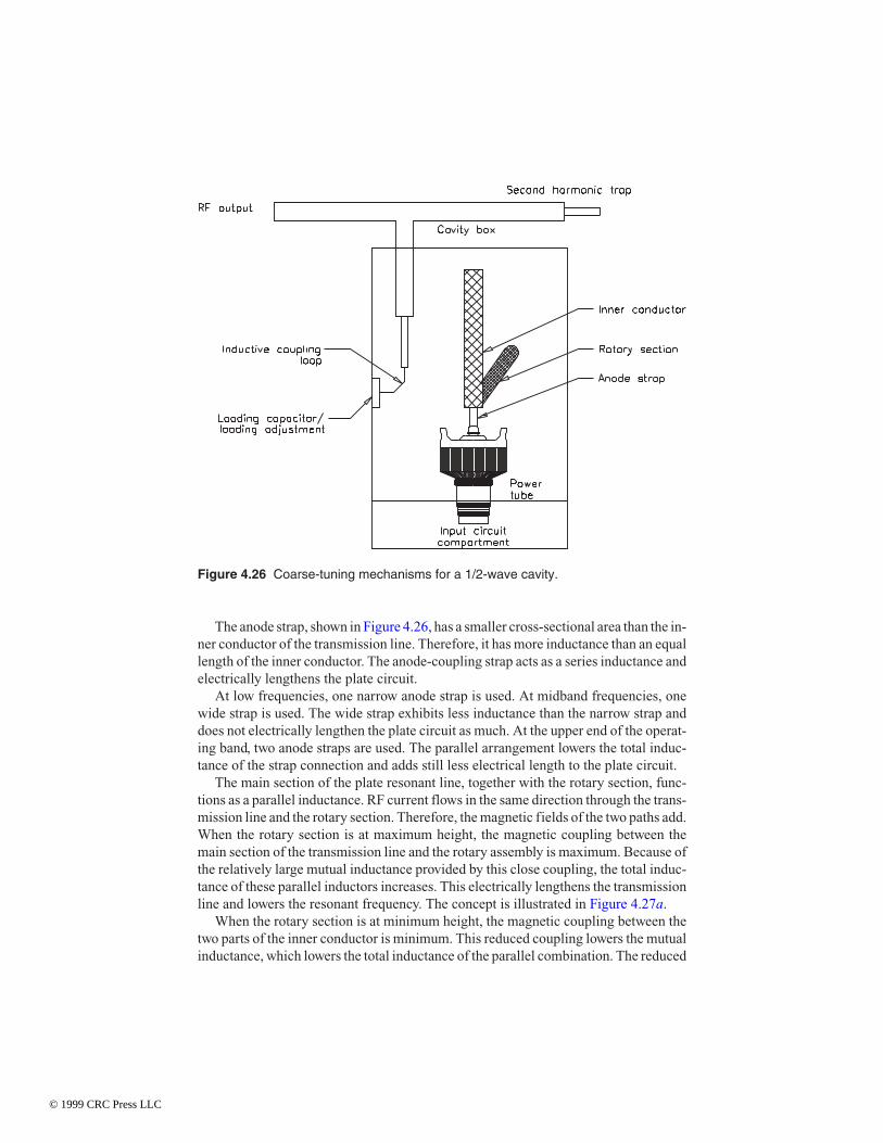
The anode strap, shown in Figure 4.26, has a smaller cross-sectional area than the in-ner conductor of the transmission line. Therefore, it has more inductance than an equallength of the inner conductor. The anode-coupling strap acts as a series inductance andelectrically lengthens the plate circuit.
At low frequencies, one narrow anode strap is used. At midband frequencies, onewide strap is used. The wide strap exhibits less inductance than the narrow strap anddoes not electrically lengthen the plate circuit as much. At the upper end of the operat-ing band, two anode straps are used. The parallel arrangement lowers the total induc-tance of the strap connection and adds still less electrical length to the plate circuit.
The main section of the plate resonant line, together with the rotary section, func-tions as a parallel inductance. RF current flows in the same direction through the trans-mission line and the rotary section. Therefore, the magnetic fields of the two paths add.When the rotary section is at maximum height, the magnetic coupling between themain section of the transmission line and the rotary assembly is maximum. Because ofthe relatively large mutual inductance provided by this close coupling, the total induc-tance of these parallel inductors increases. This electrically lengthens the transmissionline and lowers the resonant frequency. The concept is illustrated in Figure 4.27a.
When the rotary section is at minimum height, the magnetic coupling between thetwo parts of the inner conductor is minimum. This reduced coupling lowers the mutualinductance, which lowers the total inductance of the parallel combination. The reduced
Figure 4.26 Coarse-tuning mechanisms for a 1/2-wave cavity.
© 1999 CRC Press LLC

inductance allows operation at a higher resonant frequency. This condition is illustratedin Figure 4.27b. The rotary section provides an infinite number of coarse settings forvarious operating frequencies.
The movable plate-tune assembly is located at the end of the inner-plate transmis-sion line. It can be moved up and down to change the physical length of the inner con-ductor by about 4-3/4 in. This assembly is linked to the front-panel plate-tuning knob,providing a fine adjustment for cavity resonance.
Figure 4.27 Using the cavity's movable section to adjust for resonance: (a) the rotarysection at maximum height, (b) the rotary section at minimum height.
(a)
(b)
© 1999 CRC Press LLC

4.3.5 Folded 1/2-Wavelength Cavity
A special case of the 1/2-wavelength PA cavity is shown in Figure 4.28. The designemploys a folded 1/2-wave resonator constructed with coaxial aluminum and coppertubing. This cavity arrangement eliminates the high-voltage blocking capacitor andhigh-current shorting contacts of conventional designs by connecting the main trans-mission-line resonant circuit conductor directly to the anode of the power tube. Agrounded, concentric transmission-line center conductor tunes the cavity with a vari-able reentrant length inserted into the end of the main conductor opposite the tube.
The main conductor (the fixed portion of the plate line) is insulated from ground andcarries the anode dc potential. High-voltage power is fed at the fundamental-frequencyRF voltage null point, approximately 1/4 wavelength from the anode, for easy RF de-coupling. A large surface area without sliding contacts results in minimal loss.
Incorporated into the tank design is a second harmonic suppressor. Rather than at-tenuating the second harmonic after the signal has been generated and amplified, thisdesign essentially prevents formation of second-harmonic energy by series-LC trap-ping the second-harmonic waveform at the point where the wave exhibits a high imped-
Figure 4.28 The basic design of a folded 1/2-wavelength cavity.
© 1999 CRC Press LLC

ance (approximately 1/4 wavelength from the anode). The second harmonic will peakin voltage at the same point that the dc-plate potential is applied.
Plate tuning is accomplished by an adjustable bellows on the center portion of theplate line, which is maintained at chassis ground potential. Output coupling is accom-plished with an untuned loop intercepting the magnetic field concentration at the volt-age null (maximum RF current) point of the main line. The PA loading control variesthe angular position of the plane of the loop with respect to the plate line, changing theamount of magnetic field that it intercepts. Multiple phosphor-bronze leaves connectone side of the output loop to ground and the other side to the center conductor of theoutput transmission line. This allows for mechanical movement of the loop by the PAloading control without using sliding contacts. The grounded loop improves immunityto lightning and to static buildup on the antenna.
4.3.6 Wideband Cavity
The cavity systems discussed so far in this section provide adequate bandwidth formany applications. Some uses, however, dictate an operating bandwidth beyond whata conventional cavity amplifier can provide. One method of achieving wider operat-ing bandwidth involves the use of a double-tuned overcoupled amplifier, shown inFigure 4.29. The system includes four controls to accomplish tuning:
• Primary tune, which resonates the plate circuit and tends to tilt the response andslide it up and down the bandpass.
• Coupling, which sets the bandwidth of the PA. Increased coupling increases theoperating bandwidth and lowers the PA efficiency. When the coupling is ad-justed, it can tilt the response and change the center of the bandpass, necessitatingreadjustment of the plate-tune control.
• Secondary tune, which resonates the secondary cavity and will tilt the response ifso adjusted. The secondary tune control typically can be used to slide the responseup and down the bandpass, similar to the primary tune control.
• Loading, which determines the value of ripple in the bandpass response. Adjust-ment of the loading control usually tilts the response and changes the bandwidth,necessitating readjustment of the secondary tune and coupling controls.
4.3.7 Output Coupling
Coupling is the process by which RF energy is transferred from the amplifier cavity tothe output transmission line. Wideband cavity systems use coupling to transfer energyfrom the primary cavity to the secondary cavity. Coupling in tube-type power amplifi-ers usually transforms a high (plate or cavity) impedance to a lower output (transmis-sion line) impedance. Both capacitive (electrostatic) and inductive (magnetic) cou-pling methods are used in cavity RF amplifiers. In some designs, combinations of thetwo methods are used.
© 1999 CRC Press LLC

Inductive Coupling
Inductive (magnetic) coupling employs the principles of transformer action. The effi-ciency of the coupling depends upon three conditions:
• The cross-sectional area under the coupling loop, compared to the cross-sectionalarea of the cavity (see Figure 4.30). This effect can be compared to the turns ratioprinciple of a transformer.
• The orientation of the coupling loop to the axis of the magnetic field. Couplingfrom the cavity is proportional to the cosine of the angle at which the couplingloop is rotated away from the axis of the magnetic field, as illustrated in Figure4.31.
• The amount of magnetic field that the coupling loop intercepts (see Figure 4.32).The strongest magnetic field will be found at the point of maximum RF current inthe cavity. This is the area where maximum inductive coupling is obtained.Greater magnetic field strength also is found closer to the center conductor of thecavity. Coupling, therefore, is inversely proportional to the distance of the cou-pling loop from the center conductor.
Figure 4.29 Double-tuned overcoupled broadband cavity amplifier.
© 1999 CRC Press LLC

In both 1/4- and 1/2-wavelength cavities, the coupling loop generally feeds a 50 Ωtransmission line (the load). The loop is in series with the load and has considerable in-ductance at very high frequencies. This inductance will reduce the RF current thatflows into the load, thus reducing power output. This effect can be overcome by placinga variable capacitor in series with the output coupling loop. The load is connected toone end of the coupling loop, and the variable capacitor ties the other end of the loop to
Figure 4.30 The use of inductive coupling in a 1/4-wavelength PA stage.
Figure 4.31 Top view of a cavity showing the inductive coupling loop rotated away fromthe axis of the magnetic field of the cavity.
© 1999 CRC Press LLC

ground. The variable capacitor cancels some or all of the loop inductance. It functionsas the PA-stage loading control.
Maximum loop current and output power occurs when the loading capacitor cancelsall of the inductance of the loading loop. This lowers the plate impedance and results inheavier loading.
Light loading results if the loading capacitance does not cancel all of the loop induc-tance. The loop inductance that is not canceled causes a decrease in load current andpower output, and an increase in plate impedance.
Capacitive Coupling
Capacitive (electrostatic) coupling, which physically appears to be straightforward,often baffles the applications engineer because of its unique characteristics. Figure4.33 shows a cavity amplifier with a capacitive coupling plate positioned near its cen-ter conductor. This coupling plate is connected to the output load, which may be atransmission line or a secondary cavity (for wideband operation). The parameters thatcontrol the amount of capacitive coupling include:
• The area of the coupling capacitor plate (the larger the area, the greater the cou-pling)
• The distance from the coupling plate to the center conductor (the greater the dis-tance, the lighter the coupling)
Figure 4.32 Cutaway view of the cavity showing the coupling loop rotated away fromthe axis of the magnetic field.
© 1999 CRC Press LLC

Maximum capacitive coupling occurs when the coupling plate is at the maximumvoltage point on the cavity center conductor.
To understand the effects of capacitive coupling, observe the equivalent circuit ofthe cavity. Figure 4.34 shows the PA tube, cavity (functioning as a parallel resonant cir-cuit), and output section. The plate-blocking capacitor isolates the tube’s dc voltagefrom the cavity. The coupling capacitor and output load are physically in series, butelectrically they appear to be in parallel, as shown in Figure 4.35. The resistive compo-nent of the equivalent parallel circuit is increased by the coupling reactance. The equiv-alent parallel coupling reactance is absorbed into the parallel resonant circuit. This ex-plains the need to retune the plate after changing the PA stage coupling (loading). Thecoupling reactance may be a series capacitor or inductor.
The series-to-parallel transformations are explained by the following formula:
RR X
Rp
s s
s
=+2 2
(4.12)
XR X
Xp
s s
s
=+2 2
(4.13)
Where:Rp = effective parallel resistanceRs = actual series resistance
Figure 4.33 A 1/4-wavelength cavity with capacitive coupling to the output load.
© 1999 CRC Press LLC

Xs = actual series reactanceXp = effective parallel reactance
Figure 4.34 The equivalent circuit of a 1/4-wavelength cavity amplifier with capacitivecoupling.
Figure 4.35 The equivalent circuit of a 1/4-wavelength cavity amplifier showing how se-ries capacitive coupling appears electrically as a parallel circuit to the PA tube.
© 1999 CRC Press LLC

PA Loading
Proper loading of a cavity PA stage to the output transmission line is critical to de-pendable operation and optimum efficiency of the overall system. Light coupling pro-duces light loading and results in a high plate impedance; conversely, heavy couplingresults in heavier loading and a lower plate impedance. Maximum output power, coin-ciding with maximum efficiency and acceptable dissipation, dictates a specific plateimpedance for a cavity of given design. This plate impedance is also dependent uponthe operating values of dc plate voltage (Ep) and plate current (Ip).
Plate impedance dictates the cavity parameters of loaded Q, RF circulating current,and bandwidth. The relationships can be expressed as follows:
• Loaded Q is directly proportional to the plate impedance and controls the othertwo cavity parameters. Loaded Q = Zp/Xl, where Zp = cavity plate impedance andXl = cavity inductive reactance.
• Circulating current in the cavity is much greater (by a factor of the loaded Q) thanthe RF current supplied by the tube. Circulating current = Q × Ip, where Ip = the RFcurrent supplied to the cavity by the tube.
• The cavity bandwidth is dependent on the loaded Q and operating frequency.Bandwidth = Fr/Q, where Fr = the cavity resonant frequency.
Heavy loading lowers the PA plate impedance and cavity Q. A lower Q reduces thecavity RF circulating currents. In some cavities, high circulating currents can causecavity heating and premature failure of the plate or screen blocking capacitors. The ef-fects of lower plate impedance—a by-product of heavy loading—are higher RF and dcplate currents and reduced RF plate voltage. The instantaneous plate voltage is the re-sult of the RF plate voltage added to the dc plate voltage. The reduced swing of platevoltage causes less positive dc screen current to flow. Positive screen current flows onlywhen the plate voltage swings close to or below the value of the positive screen grid.
Light loading raises the plate impedance and cavity Q. A higher Q will increase thecavity circulating currents, raising the possibility of component overheating and fail-ure. The effects of higher plate impedance are reduced RF and dc plate current and in-creased RF and dc plate voltage excursions. The higher cavity RF or peak dc voltagesmay cause arcing in the cavity.
There is one value of plate impedance that will yield optimum output power, effi-ciency, dissipation, and dependable operation. It is dictated by cavity design and thevalues of the various dc and RF voltages and currents supplied to the stage.
Depending on the cavity design, light loading may seem deceptively attractive. Thedc plate voltage is constant (set by the power supply), and the lower dc plate current re-sulting from light loading reduces the tube’s overall dc input power. The RF outputpower may change with light loading, depending on the plate impedance and cavity de-sign, while efficiency will probably increase or, at worst, remain constant. Cautionmust be exercised with light loading, however, because of the increased RF voltagesand circulating currents that such operation creates. Possible adverse effects include
© 1999 CRC Press LLC

cavity arcing and overheating of cavity components, such as capacitors. The manufac-turer’s recommendations on PA tube loading should, therefore, be carefully observed.
Despite the many similarities among various cavity designs, each imposes its ownset of operational requirements and limitations. No two cavity systems will tune up inexactly the same fashion. Given proper maintenance, a cavity amplifier will provideyears of reliable service.
4.3.8 Mechanical Design
The operation of a cavity amplifier can be puzzling because of the nature of the majorcomponent elements. It is often difficult to relate the electrical schematic diagram tothe mechanical assembly that exists within the transmitter. Consider the PA cavityschematic diagram shown in Figure 4.36. The grounded screen stage is of conven-tional design. Decoupling of the high-voltage power supply is accomplished by C1,C2, C3, and L1. Capacitor C3 is located inside the PA chimney (cavity inner conduc-tor). The RF sample lines provide two low-power RF outputs for a modulation moni-tor or other test instrument. Neutralization inductors L3 and L4 consist of adjustablegrounding bars on the screen grid ring assembly.
Figure 4.37 shows the electrical equivalent of the PA cavity schematic diagram. The1/4-wavelength cavity acts as the resonant tank for the PA. Coarse-tuning of the cavity
Figure 4.36 Typical VHF cavity amplifier.
© 1999 CRC Press LLC

is accomplished by adjustment of the shorting plane. Fine-tuning is performed by thePA tuning control, which acts as a variable capacitor to bring the cavity into resonance.The PA loading control consists of a variable capacitor that matches the cavity to theload. The assembly made up of L2 and C6 prevents spurious oscillations within the cav-ity.
Blocking capacitor C4 is constructed of a roll of Kapton insulating materialsandwiched between two circular sections of aluminum. (Kapton is a registered trade-mark of Du Pont.) PA plate-tuning control C5 consists of an aluminum plate of largesurface area that can be moved in or out of the cavity to reach resonance. PA loadingcontrol C7 is constructed much the same as the PA tuning assembly, with a large-areapaddle feeding the harmonic filter, located external to the cavity. The loading paddlemay be moved toward the PA tube or away from it to achieve the required loading. TheL2-C6 damper assembly actually consists of a 50 Ωnoninductive resistor mounted onthe side of the cavity wall. Component L2 is formed by the inductance of the connectingstrap between the plate-tuning paddle and the resistor. Component C6 is the equivalentstray capacitance between the resistor and the surrounding cavity box.
It can be seen that cavity amplifiers involve as much mechanical engineering as theydo electrical engineering. The photographs of Figure 4.38 show graphically the level ofcomplexity that a cavity amplifier may involve. Figure 4.38a depicts a VHF power am-plifier (Philips) with broadband input circuitry. Figure 4.38b shows a wideband VHFamplifier intended for television service (Varian). Figure 4.38c illustrates a VHF cavityamplifier designed for FM broadcast service (Varian).
Figure 4.37 Electrical equivalent of the cavity amplifier shown in Figure 4.36.
© 1999 CRC Press LLC

Figure 4.38 VHF cavity amplifiers: (a) cross-sectional view of a broadband design, (b)cavity designed for television service, (c, next page) FM broadcast cavity amplifier.
(b)
(a)
© 1999 CRC Press LLC

4.4 High-Voltage Power SuppliesVirtually all power grid and microwave vacuum tubes require one or more sources ofhigh voltage to operate. The usual source of operating power is a single-phase ormultiphase supply operating from ac line current. Most supplies use silicon rectifiersas the primary ac-to-dc converting device.
4.4.1 Silicon Rectifiers
Rectifier parameters generally are expressed in terms of reverse-voltage ratings andmean forward-current ratings in a -wave rectifier circuit operating from a 60 Hz sup-ply and feeding a purely resistive load. The three principle reverse-voltage ratings are:
• Peak transient reverse voltage (Vrm). The maximum value of any nonrecurrentsurge voltage. This value must never be exceeded.
• Maximum repetitive reverse voltage (VRM(rep)). The maximum value of reversevoltage that may be applied recurrently (in every cycle of 60 Hz power). This in-cludes oscillatory voltages that may appear on the sinusoidal supply.
• Working peak reverse voltage (VRM(wkg)). The crest value of the sinusoidal voltageof the ac supply at its maximum limit. Rectifier manufacturers generally recom-mend a value that has a significant safety margin, relative to the peak transient re-verse voltage (Vrm), to allow for transient overvoltages on the supply lines.
Figure 4.38c
(c)
© 1999 CRC Press LLC

There are three forward-current ratings of similar importance in the application ofsilicon rectifiers:
• Nonrecurrent surge current (IFM,surge). The maximum device transient current thatmust not be exceeded at any time. IFM,surge is sometimes given as a single value, butmore often is presented in the form of a graph of permissible surge-current valuesvs. time. Because silicon diodes have a relatively small thermal mass, the poten-tial for short-term current overloads must be given careful consideration.
• Repetitive peak forward current (IFM,rep). The maximum value of forward-currentreached in each cycle of the 60 Hz waveform. This value does not include randompeaks caused by transient disturbances.
• Average forward current (IFM,av). The upper limit for average load current throughthe device. This limit is always well below the repetitive peak forward-currentrating to ensure an adequate margin of safety.
Rectifier manufacturers generally supply curves of the instantaneous forward volt-age vs. instantaneous forward current at one or more specific operating temperatures.These curves establish the forward-mode upper operating parameters of the device.
Figure 4.39 shows a typical rectifier application in a bridge circuit.
4.4.2 Operating Rectifiers in Series
High-voltage power supplies (5 kV and greater) often require rectifier voltage ratingswell beyond those typically available from the semiconductor industry. To meet therequirements of the application, manufacturers commonly use silicon diodes in a se-ries configuration to give the required working peak reverse voltage. For such a con-figuration to work properly, the voltage across any one diode must not exceed therated peak transient reverse voltage (Vrm) at any time. The dissimilarity commonlyfound between the reverse leakage current characteristics of different diodes of thesame type number makes this objective difficult to achieve. The problem normally is
Figure 4.39 Conventional capacitor input filter full-wave bridge.
© 1999 CRC Press LLC

overcome by connecting shunt resistors across each rectifier in the chain, as shown inFigure 4.40. The resistors are chosen so that the current through the shunt elements(when the diodes are reverse-biased) will be several times greater than the leakagecurrent of the diodes themselves.
The carrier storage effect also must be considered in the use of a series-connectedrectifier stack. If precautions are not taken, different diode recovery times (caused bythe carrier storage phenomenon) will effectively force the full applied reverse voltageacross a small number of diodes, or even a single diode. This problem can be preventedby connecting small-value capacitors across each diode in the rectifier stack. The ca-pacitors equalize the transient reverse voltages during the carrier storage recovery peri-ods of the individual diodes.
Figure 4.41 illustrates a common circuit configuration for a high-voltage 3-phaserectifier bank. A photograph of a high-voltage series-connected 3-phase rectifier as-sembly is shown in Figure 4.42.
Figure 4.40 A portion of a high-voltage series-connected rectifier stack.
Figure 4.41 A 3-phase delta-connected high-voltage rectifier.
© 1999 CRC Press LLC

4.4.3 Operating Rectifiers in Parallel
Silicon rectifiers are used in a parallel configuration when a large amount of currentis required from the power supply. Current sharing is the major design problem with aparallel rectifier assembly because diodes of the same type number do not necessarilyexhibit the same forward characteristics.
Semiconductor manufacturers often divide production runs of rectifiers into toler-ance groups, matching forward characteristics of the various devices. When parallel di-odes are used, devices from the same tolerance group must be used to avoid unequalsharing of the load current. As a margin of safety, designers allow a substantial deratingfactor for devices in a parallel assembly to ensure that the maximum operating limits ofany one component are not exceeded.
The problems inherent in a parallel rectifier assembly can be reduced through theuse of a resistance or reactance in series with each component, as shown in Figure 4.43.The buildout resistances (R1 through R4) force the diodes to share the load currentequally. Such assemblies can, however, be difficult to construct and may be more ex-pensive than simply adding diodes or going to higher-rated components.
Figure 4.42 High-voltage rectifierassembly for a 3-phasedelta-connected circuit.
© 1999 CRC Press LLC

4.4.4 Silicon Avalanche Rectifiers
The silicon avalanche diode is a special type of rectifier that can withstand high re-verse power dissipation. For example, an avalanche diode with a normal forward rat-ing of 10 A can dissipate a reverse transient of 8 kW for 10 ms without damage. Thischaracteristic of the device allows elimination of the surge-absorption capacitor andvoltage-dividing resistor networks needed when conventional silicon diodes are usedin a series rectifier assembly. Because fewer diodes are needed for a given applied re-verse voltage, significant underrating of the device (to allow for reverse-voltage tran-sient peaks) is not required.
When an extra-high-voltage rectifier stack is used, it is still advisable to install shuntcapacitors—but not resistors—in an avalanche diode assembly. The capacitors are de-signed to compensate for the effects of carrier storage and stray capacitance in a longseries assembly.
4.4.5 Thyristor Servo Systems
Thyristor control of ac power has become a common method of regulating high-volt-age power supplies. The type of servo system employed depends on the application.Figure 4.44 shows a basic single-phase ac control circuit using discrete thyristors. Therms load current (Irms) at any specific phase delay angle (α) is given in terms of thenormal full-load rms current at a phase delay of zero (Irms-0):
( )I Irms rms= − + −
−θ
απ
π α1 2 1 21 2
sin (4.14)
The load rms voltage at any particular phase-delay angle bears the same relationshipto the full-load rms voltage at zero phase delay as the previous equation illustrates forload current. An analysis of the mathematics shows that although the theoretical delayrange for complete control of a resistive load is 0 to 180°, a practical span of 20 to160° gives a power-control range of approximately 99 to 1 percent of maximum out-put to the load. Figure 4.45 illustrates typical phase-control waveforms.
Figure 4.43 Using buildout resistancesto force current sharing in a parallel recti-fier assembly.
© 1999 CRC Press LLC

The circuit shown in Figure 4.44 requires a source of gate trigger pulses that must beisolated from each other by at least the peak value of the applied ac voltage. The twogate pulse trains must also be phased 180° with respect to each other. Also, the gatepulse trains must shift together with respect to the ac supply voltage phase when powerthroughput is adjusted.
Some power-control systems use two identical, but isolated, gate pulse trains operat-ing at a frequency of twice the applied supply voltage (120 Hz for a 60 Hz system). Un-der such an arrangement, the forward-biased thyristor will fire when the gate pulses areapplied to the silicon controlled rectifier (SCR) pair. The reverse-biased thyristor will
Figure 4.44 Inverse-parallel thyristor ac power control: (a) circuit diagram, (b) voltageand current waveforms for full and reduced thyristor control angles. The waveforms ap-ply for a purely resistive load.
(a)
(b)
© 1999 CRC Press LLC

not fire. Normally, it is considered unsafe to drive a thyristor gate positive while its an-ode-cathode is reverse-biased. In this case, however, it may be permissible because thethyristor that is fired immediately conducts and removes the reverse voltage from theother device. The gate of the reverse-biased device is then being triggered on a thyristorthat essentially has no applied voltage.
Figure 4.45 Waveforms in an ac circuit using thyristor power control.
© 1999 CRC Press LLC

Inductive Loads
The waveforms shown in Figure 4.46 illustrate effects of phase control on an induc-tive load. When inductive loads are driven at a reduced conduction angle, a sharptransient change of load voltage occurs at the end of each current pulse (or loop). The
Figure 4.46 Voltage and current waveforms for inverse-parallel thyristor power controlwith an inductive load: (a) full conduction, (b) small-angle phase reduction, (c)large-angle phase reduction.
(a)
(b)
(c)
© 1999 CRC Press LLC

transients generally have no effect on the load, but they can be dangerous to properoperation of the thyristors. When the conducting thyristor turns off, thereby discon-necting the load from the ac line supply, the voltage at the load rapidly drops to zero.This rapid voltage change, in effect, applies a sharply rising positive anode voltage tothe thyristor opposing the device that has been conducting. If the thyristor dv/dt(change in voltage as a function of a change in time) rating is exceeded, the opposingdevice will turn on and conduction will take place, independent of any gate drivepulse.
A common protective approach involves the addition of a resistor-capacitor (RC)snubber circuit to control the rate of voltage change seen across the terminals of the thy-ristor pair. Whenever a thyristor pair is used to drive an inductive load, such as a powertransformer, it is critically important that each device fires at a point in the appliedwaveform exactly 180° relative to the other. If proper timing is not achieved, the posi-tive and negative current loops will differ in magnitude, causing a direct current to flowthrough the primary side of the transformer. A common trigger control circuit, there-fore, should be used to determine gate timing for thyristor pairs.
Applications
Several approaches are possible for thyristor power control in a 3-phase ac system.The circuit shown in Figure 4.47 consists of essentially three independent, but inter-locked, single-phase thyristor controllers. This circuit is probably the most commonconfiguration found in commercial and industrial equipment.
In a typical application, the thyristor pairs feed a power transformer with multitapprimary windings, thereby giving the user an adjustment range to compensate for varia-
Figure 4.47 Modified full-thyristor 3-phase ac control of an inductive delta load.
© 1999 CRC Press LLC

tions in utility company line voltages from one location to another. A common proce-dure specifies selection of transformer tap positions that yield a power output of 105percent when nominal utility company line voltages are present. The thyristorpower-control system then is used to reduce the angle of conduction of the SCR pairs asnecessary to cause a reduction in line voltage to the power transformer to yield 100 per-cent rated power output from the power supply. A servo loop from a sample point at theload may be used to compensate automatically for line-voltage variations. With such anarrangement, the thyristors are kept within a reasonable degree of retarded phase opera-tion. Line voltages will be allowed to sag 5 percent or so without affecting the dc supplyoutput. Utility supply voltage excursions above the nominal value simply will result infurther delayed triggering of the SCR pairs.
Thyristor control of high-power loads (200 kW and above) typically uses transform-ers that provide 6- or 12-phase outputs. Although they are more complicated and ex-pensive, such designs allow additional operational control, and filtering requirementsare reduced significantly. Figure 4.48 shows a 6-phase boost rectifier circuit. The con-figuration consists basically of a full-wave 3-phase SCR bridge connected to awye-configured transformer secondary. A second bridge, consisting of six diodes, isconnected to low-voltage taps on the same transformer. When the SCRs are fully on,their output is at a higher voltage than the diode bridge. As a result, the diodes are re-verse-biased and turned off. When the SCRs are partially on, the diodes are free to con-
Figure 4.48 A 6-phase boost rectifier circuit.
© 1999 CRC Press LLC
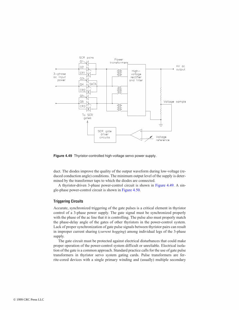
duct. The diodes improve the quality of the output waveform during low-voltage (re-duced conduction angle) conditions. The minimum output level of the supply is deter-mined by the transformer taps to which the diodes are connected.
A thyristor-driven 3-phase power-control circuit is shown in Figure 4.49. A sin-gle-phase power-control circuit is shown in Figure 4.50.
Triggering Circuits
Accurate, synchronized triggering of the gate pulses is a critical element in thyristorcontrol of a 3-phase power supply. The gate signal must be synchronized properlywith the phase of the ac line that it is controlling. The pulse also must properly matchthe phase-delay angle of the gates of other thyristors in the power-control system.Lack of proper synchronization of gate pulse signals between thyristor pairs can resultin improper current sharing (current hogging) among individual legs of the 3-phasesupply.
The gate circuit must be protected against electrical disturbances that could makeproper operation of the power-control system difficult or unreliable. Electrical isola-tion of the gate is a common approach. Standard practice calls for the use of gate pulsetransformers in thyristor servo system gating cards. Pulse transformers are fer-rite-cored devices with a single primary winding and (usually) multiple secondary
Figure 4.49 Thyristor-controlled high-voltage servo power supply.
© 1999 CRC Press LLC

windings that feed, or at least control, the individual gates of a back-to-back thyristorpair. This concept is illustrated in Figure 4.51. Newer thyristor designs may useoptocouplers to achieve the necessary electrical isolation between the trigger circuitand the gate.
It is common practice to tightly twist together the control leads from the gate andcathode of a thyristor to the gating card assembly. This practice provides a degree of im-munity to high-energy pulses that might inadvertently trigger the thyristor gate. Thegate circuit must be designed and configured carefully to reduce inductive and capaci-tive coupling that might occur between power and control circuits. Because of the highdi/dt (change in current as a function of a change in time) conditions commonly foundin thyristor-controlled power circuits, power wiring and control (gate) wiring must beseparated physically as much as possible. Shielding of gating cards in a metal card cageis advisable.
Equipment manufacturers use various means to decrease gate sensitivity to transientsources, including placement of a series resistor in the gate circuit and/or a shunting ca-pacitor between the gate and cathode. A series resistor has the effect of decreasing gatesensitivity, increasing the allowable dv/dt of the thyristor and reducing the turn-offtime, which simultaneously increases the required holding and latching currents. Theuse of a shunt capacitor between the gate and cathode leads reduces high-frequencynoise components that might be present on the gate lead and increases the dv/dt with-stand capability of the thyristor.
Figure 4.50 Phase-controlled power supply with primary regulation.
© 1999 CRC Press LLC

Fusing
Current limiting is a basic method of protection for any piece of equipment operatedfrom the utility ac line. The device typically used for breaking fault currents is either afuse or a circuit breaker. Some designs incorporate both components. Semiconductorfuses often are used in conjunction with a circuit breaker to provide added protection.Semiconductor fuses operate more rapidly (typically within 8.3 ms) and more predict-ably than common fuses or circuit breakers. Surge currents caused by a fault can de-stroy a semiconductor device, such as a power thyristor, before the ac line circuitbreaker has time to act. Manufacturers of semiconductor fuses and thyristors usuallyspecify in their data sheets the I2t ratings of each device. Because the thyristor ratingnormally assumes that the device is operating at maximum rated current and maxi-mum junction temperature (conditions that do not represent normal operation), asafety factor is ensured.
Control Flexibility
Thyristor servo control of a high-voltage power supply is beneficial to the user for anumber of reasons, including:
• Wide control over ac input voltages
Figure 4.51 Simplified block diagram of the gating circuit for a phase-control system us-ing back-to-back SCRs.
© 1999 CRC Press LLC

• Capability to compensate automatically for line-voltage variations
• Capability to soft-start the dc supply
Thyristor control circuits typically include a ramp generator that increases the ac linevoltage to the power transformer from zero to full value within 2 to 5 s. This preventshigh surge currents through rectifier stacks and filter capacitors during systemstartup.
Although thyristor servo systems are preferred over other power-control approachesfrom an operational standpoint, they are not without their drawbacks. The control sys-tem is complex and can be damaged by transient activity on the ac power line. Conven-tional power contactors are simple and straightforward. They either make contact orthey do not. For reliable operation of the thyristor servo system, attention must be givento transient suppression at the incoming power lines.
4.4.6 Polyphase Rectifier Circuits
High-voltage power supplies typically used in vacuum tube circuits incorporatemultiphase rectification of the ac line voltage. Common configurations include 3-, 6-,and 12-phase, with 3-phase rectification being the most common. Figure 4.52 illus-trates four approaches to 3-phase rectification:
• Three-phase half-wave wye, Figure 4.52a. Three half-wave rectifiers are used ineach leg of the secondary wye forming one phase. In such an arrangement, eachdiode carries current one-third of each cycle, and the output wave pulses at threetimes the frequency of the ac supply. In order to avoid direct-current saturation inthe transformer, it is necessary to employ a 3-phase transformer rather than threesingle-phase transformers.
• Three-phase full-wave bridge, Figure 4.52b. Six diodes are used in this circuit toproduce a low ripple output with a frequency of six times the input ac waveform.It is permissible in this configuration to use three single-phase transformers, if de-sired.
• Six-phase star, Figure 4.52c. This circuit, also known as a 3-phase diametric con-figuration, uses six diodes with a transformer secondary configured as a star, as il-lustrated in the figure. The output ripple frequency is six times the input ac wave-form.
• Three-phase double-wye, Figure 4.52d. This circuit uses six diodes and a compli-cated configuration of transformer windings. Note the balance coil (interphasetransformer) in the circuit.
The relative merits of these rectifier configurations are listed in Table 4.3.Polyphase rectifiers are used when the dc power required is on the order of 2 kW or
more. The main advantages of a polyphase power supply over a single-phase supply in-clude the following:
• Division of the load current between three or more lines to reduce line losses.
© 1999 CRC Press LLC

Figure 4.52 Basic 3-phase rectifier circuits: (a) half-wave wye, (b) full-wave bridge, (c)6-phase star, (d) 3-phase double-wye.
(a)
(b)
(c)
(d)
© 1999 CRC Press LLC

Table 4.3 Operating Parameters of 3-Phase Rectifier Configurations
Parameter 3-PhaseStar
3-PhaseBridge
6-PhaseStar
3-PhaseDouble-Y
Multiplier1
Rectifier elements 3 6 6 6Rms dc voltage out-put
1.02 1.00 1.00 1.00 Average dc voltageoutput
Peak dc voltageoutput
1.21 1.05 1.05 1.05 Average dc voltageoutput
Peak reverse voltsper rectifier
2.09 1.05 2.09 2.42 Average dc voltageoutput
2.45 2.45 2.83 2.83 Rms secondaryvolts per trans-former leg
1.41 1.41 1.41 1.41 Rms secondaryvolts line-to-line
Average dc outputcurrent per rectifier
0.333 0.333 0.167 0.167 Average dc outputcurrent
Rms current perrectifier, resistiveload
0.587 0.579 0.409 0.293 Average dc outputcurrent
Rms current perrectifier, inductiveload
0.578 0.578 0.408 0.289 Average dc outputcurrent
Percent ripple 18.3 4.2 4.2 4.2Ripple frequency 3 6 6 6 Line frequencyAC line power fac-tor
0.826 0.955 0.955 0.955
Transformer sec-ondary rms voltsper leg2
0.855 0.428 0.740 0.855 Average dc voltageoutput
Transformer sec-ondary rms voltsline-to-line
1.48 0.740 1.48(max)
1.71(max, noload)
Average dc voltageoutput
Secondary line cur-rent
0.578 0.816 0.408 0.289 Average dc outputcurrent
Transformer sec-ondaryvolt-amperes
1.48 1.05 1.81 1.48 DC watts output
Primary line current 0.817 1.41 0.817 0.707 (Avg. load I x sec-ondary leg V) / pri-mary line V
1 To determine the value of a parameter in any column, multiply the factor shown by the valuegiven in this column.
2 For inductive load or large choke input filter.
© 1999 CRC Press LLC

• Significantly reduced filtering requirements after rectification because of the lowripple output of a polyphase rectifier.
• Improved voltage regulation when using an inductive-input filter. Output voltagesoaring is typically 6 percent or less from full-load to no-load conditions.
• Greater choice of output voltages from a given transformer by selection of eithera delta or wye configuration.
The main disadvantage of a polyphase system is its susceptibility to phase imbalance.Resulting operational problems include increased ripple at the output of the supplyand uneven sharing of the load current by the transformer windings.
4.4.7 Power Supply Filter Circuits
A filter network for a high-voltage power supply typically consists of a series induc-tance and one or more shunt capacitances. Bleeder resistors and various circuit pro-tection devices are usually incorporated as well. Filter systems can be divided intotwo basic types:
• Inductive input: filter circuits that present a series inductance to the rectifier out-put
• Capacitive input: filter circuits that present a shunt capacitance to the rectifieroutput
Inductive Input Filter
The inductive input filter is the most common configuration found in high-power RFequipment. A common circuit is shown in Figure 4.53, along with typical currentwaveforms. When the input inductance is infinite, current through the inductance isconstant and is carried at any moment by the rectifier anode that has the most positivevoltage applied to it at that instant. As the alternating voltage being rectified passesthrough zero, the current suddenly transfers from one anode to another, producingsquare current waves through the individual rectifier devices.
When the input inductance is finite (but not too small), the situation changes to thatshown by the solid lines of Figure 4.53. The current through the input inductance tendsto increase when the output voltage of the rectifier exceeds the average or dc value, andto decrease when the rectifier output voltage is less than the dc value. This causes thecurrent through the individual anodes to be modified as shown. If the input inductanceis too small, the current decreases to zero during a portion of the time between the peaksof the rectifier output voltage. The conditions then correspond to a capacitor input filtersystem.
© 1999 CRC Press LLC

Figure 4.53 Voltage and current waveshapes for an inductive-input filter driven by a3-phase supply.
© 1999 CRC Press LLC

The output wave of the rectifier can be considered as consisting of a dc componentupon which are superimposed ac voltages (ripple voltages). To a first approximation,the fluctuation in output current resulting from a finite input inductance can be consid-ered as the current resulting from the lowest-frequency component of the ripple voltageacting against the impedance of the input inductance. This assumption is permissiblebecause the higher-frequency components in the ripple voltage are smaller, and at thesame time encounter higher impedance. Furthermore, in practical filters the shuntingcapacitor following the input inductance has a small impedance at the ripple frequencycompared with the reactance of the input inductance. The peak current resulting from afinite input inductance, therefore, is given approximately by the relation [1]:
I
I
E
E
E
L
f
i
eff= +1 1
0 1ω(4.15)
Where:If = peak current with finite input inductanceIi = peak current with infinite input inductanceE1/E0 = ratio of lowest-frequency ripple component to the dc voltage in the rectifier
outputReff = effective load resistanceω L1 = reactance of the incremental value of the input inductance at the lowest rip-
ple frequency
This equation is derived as follows:
• The peak alternating current through the input inductance is approximatelyE L1 1ω
• The average or dc current is E Reff0
• The peak current with finite inductance is, therefore: ( ) ( )E L E Reff1 1 0ω +
• The current with infinite inductance is E Reff0
The effective load resistance value consists of the actual load resistance plus filter re-sistance plus equivalent diode and transformer resistances.
The normal operation of an inductive input filter requires that there be a continuousflow of current through the input inductance. The peak alternating current flowingthrough the input inductance, therefore, must be less than the dc output current of therectifier. This condition is realized by satisfying the approximate relation:
ω L RE
Eeff1
1
0
= (4.16)
In the practical case of a 60 Hz single-phase full-wave rectifier circuit, the foregoingequation becomes:
© 1999 CRC Press LLC

LReff
11130
= (4.17)
In a polyphase system, the required value of L1 is significantly less. The higher theload resistance (the lower the dc load current), the more difficult it is to maintain acontinuous flow of current and, with a given L1, the previous equation will not be sat-isfied when the load resistance exceeds a critical value.
The minimum allowable input inductance (ωL1) is termed the critical inductance.When the inductance is less than the critical value, the filter acts as a capacitor input cir-cuit. When the dc drawn from the rectifiers varies, it is still necessary to satisfy the ωL1
equation at all times, particularly if good voltage regulation is to be maintained. To ful-fill this requirement at small load currents without excessive inductance, it is necessaryto place a bleeder resistance across the output of the filter system in order to limit Reff toa value corresponding to a reasonable value of L1.
Capacitive Input Filter
When a shunt capacitance rather than a series inductance is presented to the output ofa rectifier, the behavior of the circuit is greatly modified. Each time the positive crestalternating voltage of the transformer is applied to one of the rectifier anodes, the in-put capacitor charges up to just slightly less than this peak voltage. The rectifier thenceases to deliver current to the filter until another anode approaches its peak positivepotential, when the capacitor is charged again. During the interval when the voltageacross the input capacitor is greater than the potential of any of the anodes, the voltageacross the input capacitor drops off nearly linearly with time, because the first filterinductance draws a substantially constant current from the input capacitor. A typicalset of voltage and current waves is illustrated in Figure 4.54.
The addition of a shunt capacitor to the input of a filter produces fundamentalchanges in behavior, including the following:
• The output voltage is appreciably higher than with an inductance input.
• The ripple voltage is less with a capacitance input filter than with an inductanceinput filter.
• The dc voltage across the filter input drops as the load current increases for the ca-pacitive input case, instead of being substantially constant as for the inductive in-put case.
• The ratio of peak-to-average anode current at the rectifiers is higher in the capaci-tive case.
• The utilization factor of the transformer is less with a capacitive input configura-tion.
Filters incorporating shunt capacitor inputs generally are employed when theamount of dc power required is small. Inductance input filters are used when theamount of power involved is large; the higher utilization factor and lower peak current
© 1999 CRC Press LLC

result in important savings in rectifier and transformer costs under these conditions. In-ductance input systems are almost universally employed in polyphase rectifiers.
4.5 Parameter Sampling CircuitsMost RF system parameters can be reduced to a sample voltage by using voltage di-viders or current-sense resistors in the circuit to be measured [2]. Remote metering isaccomplished by sending a signal representing the sample voltage to the remote me-tering point, and then displaying a value representing the original parameter. In prac-tice, the actual sampling ratio (sample voltage/parameter value) is not particularly im-portant as long as the sampling ratio is stable and the sample voltage is reasonable
Figure 4.54 Characteristics of a capacitive input filter circuit: (a) schematic diagram, (b)voltage waveshape across the input capacitor, (c) waveshape of current flowingthrough the diodes.
(a)
(b)
(c)
© 1999 CRC Press LLC

(i.e., low enough to be easily handled, yet high enough to be immune to noise). Figure4.55 shows some typical voltage sampling circuits for high-power RF systems.
Figure 4.55a shows how a voltage divider can be used to sample plate voltage. Thecircuit is independent of the transmitter front panel plate voltage meter. A zener clamp-ing diode is placed across the sample line for safety; if the shunt resistor opened, the fullplate voltage would be present at the sampling output terminals (assuming minimalloading by the remote indicator). The zener will typically fail in a short-circuit mode,protecting the external sampling equipment.
The sampling circuit of Figure 4.55a is adequate for systems that measure plate volt-age from a ground reference. In the event that the cathode operates at a potential otherthan ground, the sampling circuit of Figure 4.55b may be used. The sampling line is bal-anced, with both terminals floating above ground by 1 kΩThe differential output volt-age is independent of the common mode input voltage if all the resistors are preciselymatched.
Several techniques are available for dealing with differential sampling voltages(where neither side of the sample is grounded). Typical approaches include the follow-ing:
• Isolation amplifier. Isolation amplifiers provide isolation between the input andoutput by using magnetic, capacitive, optical, or thermal coupling between the in-
Figure 4.55 Plate voltage sampling circuits: (a) single-ended, (b) differential.
(a) (b)
© 1999 CRC Press LLC

put and output. Some units include feedback techniques to reduce nonlinearitiesinduced by the coupling method.
• Differential amplifier. In most cases, electrical isolation between the samplingcircuit and the remote metering equipment is not required. Instead, a differentialvoltage must be changed to a single ended voltage (one side grounded). This canbe accomplished using the differential amplifier shown in Figure 4.56a or the in-strumentation amplifier shown in Figure 4.56b.
Measurement of plate and/or screen current is typically done by inserting a sam-pling resistor into the ground return lead of the respective supplies. This approach isshown in Figure 4.57. Notice that the remote plate current metering is taken across R1,with balancing resistors of 1.2 kΩused to lift the sample above the ground reference. Abidirectional zener diode is placed across the output of the sample terminals for protec-tion. The plate current meter on the transmitter is sampled across R2, and the over-cur-rent relay is sampled across R3. Device X1 is a crowbar that will shunt the plate currentto ground in the event of a failure in the R1–R3 chain.
The initial tolerance of resistors used as current sense elements or in a voltage di-vider circuit is usually not particularly critical. An inexact resistance will cause thesample voltage to be something other than that expected. However, whatever samplevoltage appears, the remote meter can be calibrated to agree with the local meter. Themore important attribute is resistance changes with time and temperature.
Figure 4.56 Differential amplifier circuits: (a) basic circuit, (b) instrumentation amplifier.
(a) (b)
© 1999 CRC Press LLC

Figure 4.57 Transmitter high-voltage power supply showing remote plate current and voltage sensing circuits.
© 1999 C
RC
Press LL
C

A carbon composition resistor can commonly have a temperature coefficient ofabout ±600 ppm/C° for resistors up to 1 KΩ. This increases to ±1875 ppm/C° for resis-tors up to 1 MΩ. If these resistors were used in a common plate voltage sampling circuit,such as than shown in Figure 4.57, the sample voltage could change as much as 20 per-cent over a 0 C° to 50 C° temperature range. Metal film resistors are available withtemperature coefficients as low as 15 ppm/C° . Bulk metal resistors are available withtemperature coefficients of 5 ppm/C° . If the resistors in a voltage divider are at thesame temperature, the matching between the temperature coefficient of resistance(TCR) is more important than the actual TCR. Because the TCR matching is generallybetter than the TCR of an individual resistor, sampling systems should be designed tokeep the resistors in the network at the same operating temperature.
In differential amplifiers, the matching of resistor values is critical. To insure the re-sistance values track with temperature, it is common practice to use a resistor networkmade using hybrid film techniques or integrated circuit techniques. Because the resis-tors are made at the same time and of the same materials, the TCRs track closely.
4.6 References1. Terman, F. E., Radio Engineering, 3rd. Ed., McGraw-Hill, New York, pg. 560,
1947.2. Hallikainen, Harold, “Transmitter Control Systems,” in NAB Engineering Hand-
book, 9th Ed., Jerry C. Whitaker (ed.), National Association of Broadcasters, Wash-ington, D.C., 1998.
4.7 BibliographyCrutchfield, E. B. (ed.), NAB Engineering Handbook, 8th Ed., National Association of
Broadcasters, Washington, DC, 1992.Gray, T. S., Applied Electronics, Massachusetts Institute of Technology, 1954.Heising, R. A., “Modulation in Radio Telephony,” Proceedings of the IRE, Vol. 9, no.
3, pg. 305, June 1921.Heising, R. A., “Transmission System,” U.S. Patent no. 1,655,543, January 1928.Jordan, Edward C. (ed.), Reference Data for Engineers: Radio, Electronics, Com-
puters, and Communications, 7th Ed., Howard W. Sams, Indianapolis, IN, 1985.Laboratory Staff, The Care and Feeding of Power Grid Tubes, Varian Eimac, San
Carlos, CA, 1984.Martin, T. L., Jr., Electronic Circuits, Prentice Hall, Englewood Cliffs, NJ, 1955.Mendenhall, G. N., M. B. Shrestha, and E. J. Anthony, “FM Broadcast Transmitters,”
in NAB Engineering Handbook, 8th Ed., E. B. Crutchfield (ed.), National Associa-tion of Broadcasters, Washington, DC, pp. 429–474, 1992.
Shrestha, Mukunda B., “Design of Tube Power Amplifiers for Optimum FM Transmit-ter Performance,” IEEE Transactions on Broadcasting, Vol. 36, no. 1, IEEE, NewYork, pp. 46–64, March 1990.
Terman, F. E., and J. R. Woodyard, “A High Efficiency Grid-Modulated Amplifier,”Proceedings of the IRE, Vol. 26, no. 8, pg. 929, August 1938.
Terman, F. E., Radio Engineering, 3rd. Ed., McGraw-Hill, New York, 1947.
© 1999 CRC Press LLC

Weirather, R. R., G. L. Best, and R. Plonka, “TV Transmitters,” in NAB EngineeringHandbook, 8th Ed., E. B. Crutchfield (ed.), National Association of Broadcasters,Washington, DC, pp. 499–551, 1992.
Whitaker, Jerry C., AC Power Systems, 2nd Ed., CRC Press, Boca Raton, FL, 1998.Whitaker, Jerry C., Radio Frequency Transmission Systems: Design and Operation,
McGraw-Hill, New York, 1991.Woodard, George W., “AM Transmitters,” in NAB Engineering Handbook, 8th Ed.,
E. B. Crutchfield (ed.), National Association of Broadcasters, Washington, DC, pp.353–381, 1992.
© 1999 CRC Press LLC

Whitaker, Jerry C. “Chapter 5 – Applying Vacuum Tube Devices” Power Vacuum Tubes Handbook 2nd Edition.Ed. Jerry C. WhitakerBoca Raton: CRC Press LLC, 2000
© 1999 CRC Press LLC

Chapter
5Applying Vacuum Tube Devices
5.1 IntroductionNumerous circuits have been developed to meet the varied needs of high-power RFamplification. Designers have adapted standard vacuum tube devices to specific ap-plications that require unique performance criteria. Most of these circuits are builtupon a few basic concepts.
5.2 AM Power Amplification SystemsClass C plate modulation is the classic method of producing an AM waveform [1].Figure 5.1 shows the basic circuit. Triodes and tetrodes may be used as the modulatoror carrier tube. Triodes offer the simplest and most common configuration.
Numerous variations on the basic design exist, including a combination of plate andscreen grid modulation. The carrier signal is applied to the control grid, and the modu-lating signal is applied to the screen and plate. The plate is fully modulated, and thescreen is modulated 70 to 100 percent to achieve 100 percent carrier modulation. Mod-ulation of the screen can be accomplished using one of the following methods:
• Screen voltage supplied through a dropping resistor connected to theunmodulated dc plate supply, shown in Figure 5.2a
• An additional (third) winding on the modulation transformer, illustrated in Figure5.2b
• A modulation choke placed in series with a low-voltage fixed screen supply,shown in Figure 5.2c
Depending on the design, screen/plate modulation also may require partial modula-tion of the control grid to achieve the desired performance characteristics.
During the portion of the modulation cycle when the plate voltage is increased, thescreen current decreases. If the screen is supplied through an impedance, such as thescreen dropping resistance of a modulation choke, the voltage drop in this series imped-ance becomes less and the screen voltage rises in the desired manner. During the part ofthe modulation cycle when the plate voltage is decreased, the screen current increases,
© 1999 CRC Press LLC

causing a greater voltage drop in the screen series impedance, and lowering the voltageon the screen of the tube. The value of the screen bypass capacitor in the class C stage isa compromise between good RF bypassing and the shunting effect of this capacitanceon the screen modulation circuit.
5.2.1 Control Grid Modulation
Although not as common as class C plate modulation, a class C RF amplifier may bemodulated by varying the voltage on the control grid of a triode [1]. This approach,shown in Figure 5.3, produces a change in the magnitude of the plate current pulsesand, therefore, variations in the output waveform taken from the plate tank. Both thecarrier and modulation signals are applied to the grid.
The primary benefit of grid modulation is that a modulator is not required. Gridmodulation, however, requires a fixed plate supply voltage that is twice the peak RFvoltage without modulation. The result is higher plate dissipation at lower modulationlevels, including carrier level. The typical plate efficiency of a grid-modulated stagemay range from only 35 to 45 percent at carrier. Grid modulation typically is used onlyin systems where plate modulation transformers cannot provide adequate bandwidthfor the intended application.
When grid modulation is used, the screen voltage and grid bias must be taken fromsources with good regulation. This usually means separate low-voltage power supplies.
Figure 5.1 The classic plate-modulated PA circuit for AM applications.
© 1999 CRC Press LLC

5.2.2 Suppressor Grid Modulation
The output of a class C pentode amplifier may be controlled by applying a modulatingvoltage, superimposed on a suitable bias, to the suppressor grid to produce an AMwaveform [1]. As the suppressor grid becomes more negative, the minimum instanta-
Figure 5.2 Basic methods of screen and plate modulation: (a) plate modulation, (b)plate and screen modulation, (c) plate modulation using separate plate/screen supplies.
(a)
(b)
(c)
© 1999 CRC Press LLC

neous potential at which current can be drawn to the plate is increased. Thus, as mod-ulation varies the suppressor grid potential, the output voltage changes.
This method of modulating an RF amplifier provides about the same plate effi-ciency as a grid-modulated stage. The overall operating efficiency, however, is slightlylower because of increased screen grid losses associated with the design. Linearity ofthe circuit is not usually high.
5.2.3 Cathode Modulation
Cathode modulation incorporates the principles of both control grid and plate modu-lation [1]. As shown in Figure 5.4, a modulation transformer in the cathode circuitvaries the grid-cathode potential, as well as the plate-cathode potential. The ratio ofgrid modulation to plate modulation is set by adjustment of the tap shown in the fig-ure. Grid leak bias typically is employed to improve linearity of the stage.
5.2.4 High-Level AM Amplification
The basic tuned-anode vacuum tube power amplifier is described in graphical form inFigure 5.5 [2]. The tube may be a triode, tetrode, or pentode. Tetrode final amplifiersare the most common. The RF excitation voltage is applied to the grid of the PA tube,and the ratio of dc grid bias voltage to peak RF excitation voltage (shown sinusoidalin Figure 5.5) determines the conduction angle θc of anode current:
θ ccc
g cc
E
E E=
−
2 arccos (5.1)
Figure 5.3 Grid modulation of a class C RF amplifier.
© 1999 CRC Press LLC
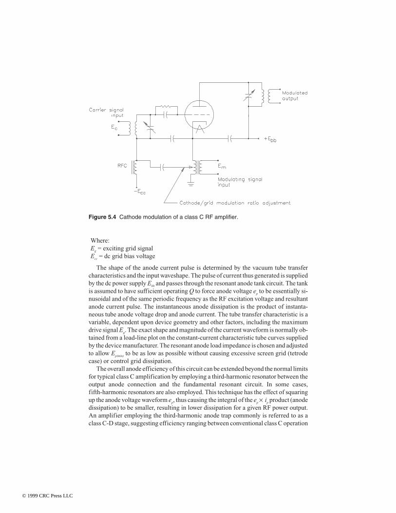
Where:Eg = exciting grid signalEcc = dc grid bias voltage
The shape of the anode current pulse is determined by the vacuum tube transfercharacteristics and the input waveshape. The pulse of current thus generated is suppliedby the dc power supply Ebb and passes through the resonant anode tank circuit. The tankis assumed to have sufficient operating Q to force anode voltage ep to be essentially si-nusoidal and of the same periodic frequency as the RF excitation voltage and resultantanode current pulse. The instantaneous anode dissipation is the product of instanta-neous tube anode voltage drop and anode current. The tube transfer characteristic is avariable, dependent upon device geometry and other factors, including the maximumdrive signal Eg. The exact shape and magnitude of the current waveform is normally ob-tained from a load-line plot on the constant-current characteristic tube curves suppliedby the device manufacturer. The resonant anode load impedance is chosen and adjustedto allow Ep(min) to be as low as possible without causing excessive screen grid (tetrodecase) or control grid dissipation.
The overall anode efficiency of this circuit can be extended beyond the normal limitsfor typical class C amplification by employing a third-harmonic resonator between theoutput anode connection and the fundamental resonant circuit. In some cases,fifth-harmonic resonators are also employed. This technique has the effect of squaringup the anode voltage waveform ep, thus causing the integral of the ep × ip product (anodedissipation) to be smaller, resulting in lower dissipation for a given RF power output.An amplifier employing the third-harmonic anode trap commonly is referred to as aclass C-D stage, suggesting efficiency ranging between conventional class C operation
Figure 5.4 Cathode modulation of a class C RF amplifier.
© 1999 CRC Press LLC

and class D operation. The use of the third-harmonic technique permits efficiencies of85 percent or more for transmitters of 10 kW power output and above.
Class B Modulator
The most common method of applying low-frequency (typically audio) intelligenceto a high-level amplitude-modulated amplifier is the class B push-pull system illus-trated in Figure 5.6 [1]. The vacuum tubes used in such a circuit may be triodes,tetrodes, or pentodes. The output circuit includes a modulation transformer, audiocoupling capacitor, and dc shunt feed inductor. The capacitor and shunt inductor net-work is used to prevent unbalanced dc from magnetizing the modulation transformercore, which would result in poor low-frequency performance. Advanced core materi-als and improved transformer design have permitted elimination of the coupling ca-
Figure 5.5 Classic vacuum tube class C amplifier: (a) representative waveforms, (b)schematic diagram. Conditions are as follows: sinusoidal grid drive, 120° anode current,resonant anode load. (After [2].)
(a)
(b)
© 1999 CRC Press LLC

pacitor and the shunt reactor in modern systems. The direct current to the modulatedRF amplifier anode, therefore, flows directly through the secondary of the modula-tion transformer.
Elimination of the coupling capacitor and shunt reactor results in improved perfor-mance from the modulator circuit. The L and C components effectively form athree-pole high-pass filter that causes low-frequency transient distortion to be gener-ated when driven with complex audio waveforms. The simplified circuit constitutes asingle-pole high-pass filter, greatly reducing low-frequency transients.
Even in the improved design, the transient distortion performance of the class Bpush-pull modulator can be insufficient for some applications. Complex modulatingwaveforms with sharp transitions present special problems. Stray internal winding ca-pacitances and leakage inductances effectively form a multipole low-pass filter at thehigh-frequency end of the audio spectrum. This filter can produce overshoots whendriven with complex waveforms. Such distortion can be reduced by filtering the inputsignal, at the cost of somewhat lower high-frequency response.
Negative feedback is used to reduce nonlinear distortion and noise in the push-pullcircuit. Negative feedback, however, usually increases high frequency transient distor-tion.
Figure 5.6 Class B push-pull modulator stage for a high-level AM amplifier.
© 1999 CRC Press LLC

5.2.5 Pulse Width Modulation
Pulse width modulation (PWM), also known as pulse duration modulation (PDM), isa common transmission system for modern vacuum tube transmitters. Figure 5.7shows the PDM scheme (Harris) applied to an amplitude-modulated PA. The PDMsystem works by utilizing a square wave switching system, illustrated in Figure 5.8.
The PDM process begins with a signal generator (Figure 5.9). A 75 kHz sine wave isproduced by an oscillator and used to drive a square wave generator, resulting in a sim-ple 75 kHz square wave. The square wave is then integrated, resulting in a triangularwaveform that is mixed with the input audio in a summing circuit. The resulting signalis a triangular waveform that rides on the incoming signal, typically audio. This com-posite signal is then applied to a threshold amplifier, which functions as a switch that isturned on whenever the value of the input signal exceeds a certain limit. The result is astring of pulses in which the width of the pulse is proportional to the period of time thetriangular waveform exceeds the threshold. The pulse output is applied to an amplifierto obtain the necessary power to drive subsequent stages. A filter eliminates whatevertransients may exist after the switching process is complete.
The PDM scheme is, in effect, a digital modulation system with the input informa-tion being sampled at a 75 kHz rate. The width of the pulses contains all the intelli-gence. The pulse-width-modulated signal is applied to a switch or modulator tube. Thetube is simply turned on, to a fully saturated state, or off in accordance with the instanta-
Figure 5.7 The pulse duration modulation (PDM) method of pulse width modulation.
© 1999 CRC Press LLC

neous value of the pulse. When the pulse goes positive, the modulator tube is turned onand the voltage across the tube drops to a minimum. When the pulse returns to its mini-mum value, the modulator tube turns off.
This PDM signal becomes the power supply to the final RF amplifier tube. When themodulator is switched on, the final amplifier will experience current flow and RF willbe generated. When the switch or modulator tube goes off, the final amplifier currentwill cease. This system causes the final amplifier to operate in a highly efficient class Dswitching mode. A dc offset voltage to the summing amplifier is used to set the carrier(no modulation) level of the transmitter.
A high degree of third-harmonic energy will exist at the output of the final amplifierbecause of the switching-mode operation. This energy is eliminated by a third-har-monic trap. The result is a stable amplifier that normally operates in excess of 90 per-cent efficiency. The power consumed by the modulator and its driver is usually a frac-tion of a full class B amplifier stage.
Figure 5.8 The principal waveforms of the PDM system.
© 1999 CRC Press LLC

The damping diode shown in Figure 5.9 is included to prevent potentially damagingtransient overvoltages during the switching process. When the switching tube turns offthe supply current during a period when the final amplifier is conducting, the high cur-rent through the inductors contained in the PDM filters could cause a large transientvoltage to be generated. The energy in the PDM filter is returned to the power supply bythe damping diode. If no alternative route were established, the energy would return byarcing through the modulator tube itself.
The PWM system makes it possible to eliminate audio frequency transformers inthe transmitter. The result is wide frequency response and low distortion. Note thatvariations on this amplifier and modulation scheme have been used by other manufac-turers for standard broadcast, shortwave service, and other applications.
5.3 Linear AmplificationThe following features are desirable for vacuum tubes used in RF linear amplifier ser-vice [1]:
• High power gain
• Low plate-to-grid capacitance
• Good efficiency
• Linear characteristics that are maintained without degradation across the desiredoperating band
For linear service, RF amplifiers may be operated in class A, AB1, AB2, or B modes.Triode, tetrode, or pentode devices may be used, either grid- or cathode-driven. Thechoice of mode, tube, and driving method depends upon the operational specifica-tions of each application.
Figure 5.9 Block diagram of a PDM waveform generator.
© 1999 CRC Press LLC

5.3.1 Device Selection
The triode tube, having a large plate-to-grid interelectrode capacitance, requires neu-tralization in grid-driven linear service to prevent oscillation [1]. A triode having alow amplification factor is suitable for class AB and AB2 grid-driven operation. TheRF grid excitation voltage for this type of service will be high; grid excursions intothe positive region are normal for class AB2. A swamping resistor should be usedacross the input tuned circuit to maintain a constant input impedance to the stage andto provide for stability. With a low value of swamping resistance, the grid currentdrawn is only a small part of the total grid load, and the driver load impedance is rela-tively constant. The swamping resistor improves RF stability by providing a low im-pedance to ground for regenerative feedback through the plate-to-grid capacitance.
High-amplification-factor triodes perform exceptionally well in circuits where thegrid is grounded and the cathode is driven. Under these conditions, the control grid actsas a shield between the input and output circuits. Neutralization, therefore, is not nor-mally required. Zero-bias triodes operate in the class AB2 mode and require only fila-ment, plate, and drive power. For optimum linear operation, a tuned circuit is placed inthe cathode RF return path to maintain a sinusoidal waveshape over the drive cycle. Thetuned circuit will reduce the intermodulation distortion produced by the amplifier andalso will reduce drive power requirements.
If the driver and PA stages are located close to each other, the tuned cathode circuitcan be a part of the output circuit of the driver. If, however, the amplifiers are far re-moved and coupled by a length of coaxial cable, it is recommended that a tuned cathodecircuit with a Q of between 2 and 4 be used.
Most tetrode and pentode amplifiers are designed to be grid-driven to take advan-tage of the high power gain of these devices.
In all linear amplifier systems, the driver output impedance should be kept low be-cause of the nonlinear input loading characteristics of the amplifier tube as it ap-proaches maximum power. The lower the driver amplifier impedance, the smaller theeffect of the nonlinear input loading.
5.3.2 Grid-Driven Linear Amplifier
A linear amplifier utilizing a tetrode or pentode is usually grid-driven to take advan-tage of the inherent high gain of the tube [1]. Such an amplifier can be driven into thegrid-current region under the proper circumstances. In any case, the input circuit willbe loaded by the tube grid. For the no-grid-current case, the driver will work into theinput conductance loading; for the grid-current case, the driver will work into the in-put conductance loading plus grid-current loading. It is therefore desirable (and nec-essary in the grid-current case) to swamp the input circuit with an appropriatenoninductive resistor. The resistor will maintain an almost constant load on the driverand minimize the effects of any nonlinearity in grid loading.
© 1999 CRC Press LLC

5.3.3 Cathode-Driven Linear Amplifier
The cathode-driven amplifier may use triode, tetrode, or pentode tubes [1]. The drivesignal is applied to the cathode in this class of operation. The cathode-driven ampli-fier is particularly suitable for high-power stages using high-µ triodes in the HF andVHF region. This class of operation normally eliminates the need for neutralizationbecause the control grid screens the plate from the input circuit. The power gain forsuitable triode class AB cathode-driven amplifiers is on the order of 7 to 20. The ac-tual tube power gain is approximately equal to the ratio of RF plate voltage to RFcathode voltage. This relationship is true because the fundamental component of theplate current is common to the input and output circuits.
Tetrode tubes also can be used in cathode-driven operation. Power gain is consider-ably higher than that of the triode, on the order of 20 to 50. It is important to note thatscreen grid current loads the input circuit, just as control-grid current does.
For an amplifier located some distance from the driver, an improvement inintermodulation distortion can be realized by tuning the cathode circuit. When thedriver is located close to the amplifier (0.1 wavelength or so) other means may be usedto minimize the nonlinear loading of the cathode-driven stage.
5.3.4 Intermodulation Distortion
When an RF signal with varying amplitude is passed through a nonlinear device,many new products are produced [1]. (Intermodulation distortion is discussed in de-tail in Section 10.3.6.) The frequency and amplitude of each component can be deter-mined mathematically because the nonlinear device can be represented by a power se-ries expanded about the zero-signal operating point. The example of a typicaltwo-tone signal serves to summarize this mathematical relationship. Assume that twoequal-amplitude test signals (f1 = 2.001 MHz, and f2 = 2.003 MHz) are applied to a lin-ear amplifier. The output spectrum of the amplifier is shown in Figure 5.10. Many ofthe distortion products fall outside the passband of the amplifier tuned circuits. If noimpedance exists at the frequencies of the distortion components, then no voltage canbe developed. Further study of this spectrum discloses that no even-order productsfall near the two desired signals. Some odd-order products, however, fall near the de-sired frequencies and possibly within the passband of the tuned circuits.
The distortion products usually given in tube data sheets are the third- and fifth-or-der intermodulation distortion products that can fall within the amplifier passband.Using the same f1 and f2 frequencies of the previous example, the frequencies of thethird-order products are:
2f1 – f2 = 1.999 MHz
2f2 – f1 = 2.005 Mhz
The frequencies of the fifth-order products are:
© 1999 CRC Press LLC

Figure 5.10 Spectrum at the output of a nonlinear device with an input of twoequal-amplitude sine waves of f1 = 2.001 MHz and f2 = 2.003 MHz.
© 1999 CRC Press LLC

3f1 – 2f2 = 1.997 MHz
3f2 – 2f1 = 2.007 MHz
These frequencies are well within the passband of a tuned circuit intended to passvoice frequencies and, therefore, power will be delivered to the antenna at these fre-quencies. All intermodulation distortion power is wasted and serves no purpose otherthan to cause interference to adjacent channels.
Intermodulation distortion in a power amplifier tube is the result of variations of thetransfer characteristics of the device from the ideal case. An ideal transfer characteristiccurve is shown in Figure 5.11. Even-order products do not contribute to theintermodulation distortion problem because they fall outside the amplifier passband.Therefore, if the transfer characteristic produces an even-order curvature at thesmall-signal end of the curve (from point A to point B) and the remaining portion of thecurve (point B to point C) is linear, the tube is considered to have an ideal transfer char-acteristic. If the operating point of the amplifier is set at point 0 (located midway hori-zontally between point A and point B), there will be no distortion in a class AB ampli-fier. However, no tube has this idealized transfer characteristic. It is possible, by manip-ulation of the electron ballistics within a given tube structure, to alter the transfer char-acteristic and minimize the distortion products.
5.4 High-Efficiency Linear AmplificationThe class B RF amplifier is the classic means of achieving linear amplification of anAM signal. A significant efficiency penalty, however, is paid for linear operation. The
Figure 5.11 Ideal grid-plate transfer curve for class AB operation.
© 1999 CRC Press LLC

plate efficiency at carrier level in a practical linear amplifier is about 33 percent,while a high-level (plate)-modulated stage can deliver a basic efficiency of 65 to 80percent. In a real-world transmitter, power consumed by the modulator stage mustalso be taken into account. However, because the output power of the modulator is, atmost, one-third of the total power output, the net efficiency of the plate-modulatedamplifier is still higher than a conventional linear amplifier of comparable power.
Still, linear amplification is attractive to the users of high-power transmitters be-cause low-level modulation can be employed. This eliminates the need for modulationtransformers and reactors, which—at certain power levels and for particular applica-tions—may be difficult to design and expensive to construct. To overcome the effi-ciency penalty of linear amplification, special systems have been designed that take ad-vantage of the benefits of a linear mode, while not imposing an excessive efficiencyburden.
5.4.1 Chireix Outphasing Modulated Amplifier
The Chireix amplifier employs two output stage tubes. The grids of the tubes aredriven with signals whose relative phase varies with the applied modulating signal.The output waveforms of the tubes are then applied to a summing network, and fi-nally to the load. Figure 5.12 shows a simplified schematic diagram.
Operation of the circuit is straightforward. When the grids of the tubes are drivenwith signals that are 180° out of phase, power output will be zero. This corresponds to anegative AM modulation peak of 100 percent. Full (100 percent) positive modulationoccurs when both grids are driven with signals that are in phase. The AM modulatingsignal is produced by varying the relative phase of the drive signals.
The phase-modulated carrier-frequency grid waveforms are generated in alow-level balanced modulator and amplified to the level required by the PA tubes. Sta-bility of the exciter in the Chireix system is critical. Any shift in the relative phase of theexciter outputs will translate to amplitude modulation of the transmitted waveform.
Because of the outphasing method employed to produce the AM signal, the powerfactor associated with the output stage is of special significance. The basic modulatingscheme would produce a unity power factor at zero output. The power factor would thendecrease with increasing RF output. To avoid this undesirable characteristic, the outputplate circuits are detuned, one above resonance and one below, to produce a specifiedoffset. This dephasing, coupled with adjustment of the relative phase of the driving sig-nals, maintains the power factor within a reasonable range.
There are, however, two major disadvantages to this system. First, the efficiency ofthe amplifier is compromised because at all instantaneous levels of modulation exceptone, the anode circuits must work into a reactive load. Typical overall efficiency is onthe order of 60 percent. Second, output carrier power adjustment is sensitive to tuningof any stage in the chain. This problem can be reduced by employing broadband ampli-fying circuits at lower-level stages.
© 1999 CRC Press LLC

5.4.2 Doherty Amplifier
The Doherty modulated amplifier has seen considerable use in high-efficiency linearAM transmitters. The system is a true high-efficiency linear amplifier, rather than ahybrid amplifier/modulator. The Doherty amplifier employs two tubes and a 90° net-work as an impedance inverter to achieve load-line modification as a function ofpower level. The basic circuit is shown in Figure 5.13.
Two tubes are used in the Doherty amplifier, a carrier tube (V1) and a peak tube(V2). The carrier tube is biased class B. Loading and drive for the tube are set to provide
Figure 5.12 Simplified schematic diagram of the Chireix outphasing modulated ampli-fier: (a) output circuit, (b) drive signal generation circuit.
(a)
(b)
© 1999 CRC Press LLC

maximum linear voltage swing at carrier level. The peak tube is biased class C; at car-rier level it just begins to conduct plate current. Each tube delivers an output powerequal to twice the carrier power when working into a load impedance of R Ω. At carrier,the reflected load impedance at the plate of V1 is equal to 2R Ω. This is the correct valueof load impedance for carrier-level output at full plate voltage swing. (The imped-ance-inverting property of the 90° network is similar to a 1/4-wave transmission line.)
A 90° phase lead network is included in the grid circuit of V1 to compensate for the90° phase lag produced by the impedance-inverting network in the plate circuit. Fornegative modulation swings, the carrier tube performs as a linear amplifier with a loadimpedance of 2R Ω; the peak tube contributes no power to the output.
On positive modulation swings, the peak tube conducts and contributes power to theR/2 load resistance. This is equivalent to connecting a negative resistance in shunt withthe R/2 load resistance, so that the value seen at the load end of the 90° network in-
Figure 5.13 Doherty high-efficiency AM amplifier: (a) operating theory, (b) schematicdiagram of a typical system.
(a)
(b)
© 1999 CRC Press LLC

creases. This increase is reflected through the network as a decrease in load resistanceat the plate of V1, causing an increase in output current from the tube, and an increase inoutput power. The drive levels on the tubes are adjusted so that each contributes thesame power (equal to twice the carrier power) at a positive modulation peak. For thiscondition, a load of R Ω is presented to each tube.
The key aspect of the Doherty circuit is the change in load impedance on tube V1with modulation. This property enables the device to deliver increased output power ata constant plate voltage swing. The result is high efficiency and good linearity. Overallefficiency of the Doherty amplifier ranges from 60 to 65 percent.
A practical application of the Doherty circuit is shown in Figure 5.13b. The shuntreactances of the phase-shift networks are achieved by detuning the related tuned cir-cuits. The tuned circuits in the grid are tuned above the operating frequency; those inthe plate are tuned below the operating frequency.
The Doherty amplifier has two important advantages in high-power applications.First, the peak anode voltage at either tube is (approximately) only one-half that re-quired for an equivalent carrier power high-level pulse width modulation (PWM) orclass B anode-modulated transmitter, thus significantly increasing reliability and us-able tube life. Second, no large modulation transformer or special filtering componentsare used in the final amplifier stages that might cause transient overshoot distortion.
Disadvantages of the Doherty amplifier include nonlinear distortion performanceand increased complexity of tuning. The major sources of nonlinear distortion includethe nonlinearity of the carrier tube at or near the 100 percent negative modulation crest,and the nonlinearity of the peak tube at or near carrier level when it is just beginning toconduct. Both sources of distortion may be effectively reduced by using moderateamounts of overall envelope feedback.
5.4.3 Screen-Modulated Doherty-Type Amplifier
A variation on the basic Doherty scheme can be found in the screen-modulated poweramplifier. The design is unique in that the system does not have to function as a linearamplifier. Instead, modulation is applied to the screen grids of both the carrier andpeak tubes. The peak tube is modulated upward during the positive half of the modu-lation cycle, and the carrier tube is modulated downward during the negative half ofthe cycle. This technique results in performance improvements over the classicDoherty design in that RF excitation voltages and modulating voltages are isolatedfrom each other, thereby eliminating a troublesome source of tuning-vs.-modulationinteraction.
The basic screen modulation system is shown in Figure 5.14. The peak and carriertubes are biased and driven in quadrature as class C amplifiers from the continuouswave RF drive source. At carrier level, the screen voltage of the carrier tube is adjustedso that the carrier device is near anode saturation and delivering approximately 96 per-cent of the carrier power. The screen voltage of the peak tube is adjusted so that it is justinto conduction, and is supplying the remaining 4 percent (approximately) of carrierpower. The combined anode efficiency at carrier level is greater than 77 percent.
© 1999 CRC Press LLC

Modulation of the carrier occurs when the screen voltage of the peak tube begins torise during the positive modulation half-cycle, thus causing the peak tube to supplymore RF current to the output load. This increase of current into the output networkcauses the resistance seen by the interanode network to increase and, because of the im-pedance-inverting characteristics of the 90° interanode network, causes a proportionaldecrease in the load impedance presented to the carrier tube.
The carrier-tube resonant anode voltage drop is fully saturated over the entire posi-tive modulation half-cycle, and therefore is effectively a constant voltage source. Thepower output of the carrier tube thus increases during the positive modulation half-cy-cle, caused by the modulated decreasing impedance at its anode, until both peak andcarrier tubes deliver twice carrier power at the 100 percent positive modulation crest.During the negative modulation half-cycle, the peak tube is held out of conduction,while the carrier-tube output voltage decreases linearly to zero output at the 100 percentmodulation trough.
A screen-modulated amplifier designed for MF operation at 1 MW is shown in Fig-ure 5.15. The carrier tube delivers all of the 1 MW carrier power to the load through the90° impedance-inverting network. When modulation is applied to the screen of the car-rier tube (during the negative half-cycle), the carrier tube output follows the modulationlinearly. Because the carrier tube is driven to full swing, its voltage excursion does notincrease during the positive half-cycle. Positive modulation is needed on the screenonly to maintain the full plate swing as the impedance load changes on the carrier tube.
The peak tube normally is operated with a negative screen voltage that maintainsplate current at near cutoff. During the positive peak of modulation, the screen of thepeak tube is modulated upward. As the peak tube is modulated positive, it deliverspower into the output circuit. As the delivered power increases, the load seen by theinterplate network changes as described for the general case.
The advantages of screen modulation are the same as those identified for theDoherty linear amplifier, plus higher efficiency at all depths of modulation. Further-
Figure 5.14 Screen-modulated Doherty-type circuit.
© 1999 CRC Press LLC

more, the screen modulation system is less sensitive to misadjustment of RF amplifiertuning.
5.4.4 Terman-Woodyard Modulated Amplifier
The Terman-Woodyard configuration uses the basic scheme of Doherty for achievinghigh efficiency (the impedance-inverting property of a 90° phase-shift network).However, the Terman-Woodyard design also employs grid modulation of both the car-rier tube and the peak tube, allowing both tubes to be operated class C. The result is anincrease in efficiency over the Doherty configuration.
The basic circuit is shown in Figure 5.16. With no modulation, V1 operates as a classC amplifier, supplying the carrier power, and V2 is biased so that it is just beginning toconduct. The efficiency at carrier is, therefore, essentially that of a class C amplifier.
During positive modulation swings, V2 conducts. At 100 percent modulation, bothtubes supply equal amounts of power to the load, as in the Doherty design. During nega-tive modulation swings, V2 is cut off, and V1 performs as a standard grid-modulatedamplifier.
The Terman-Woodyard system rates efficiency as a function of modulation percent-age for sinusoidal waveforms. Typical efficiency at carrier is 80 percent, falling to aminimum of 68 percent at 50 percent modulation and 73 percent at 100 percent modu-lation.
Figure 5.15 Practical implementation of a screen-modulated Doherty-type 1 MWpower amplifier (Continental Electronics).
© 1999 CRC Press LLC
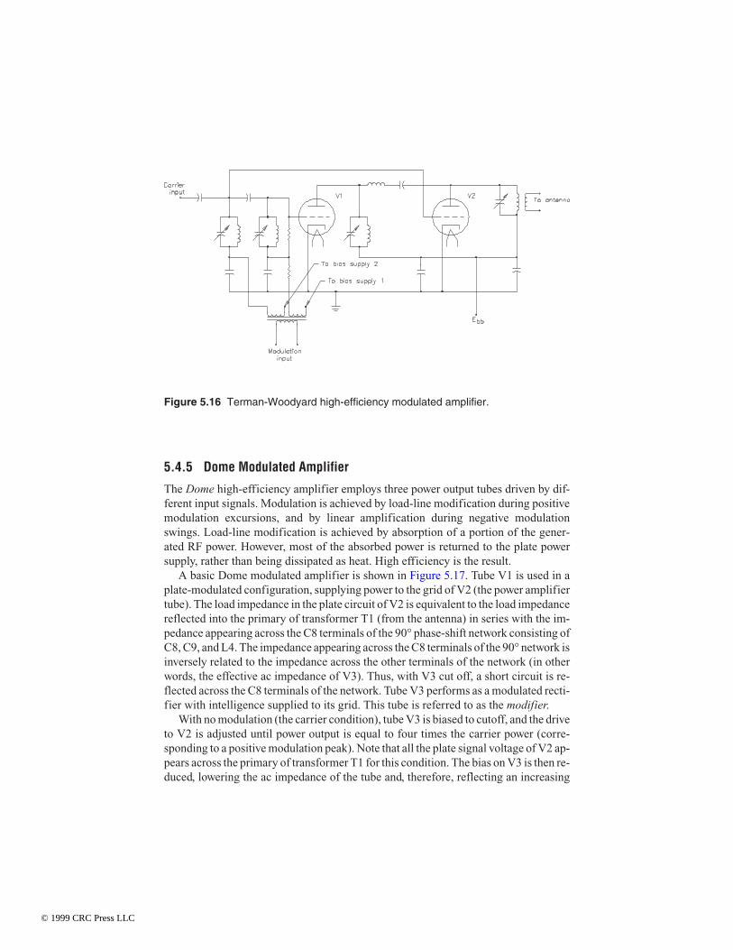
5.4.5 Dome Modulated Amplifier
The Dome high-efficiency amplifier employs three power output tubes driven by dif-ferent input signals. Modulation is achieved by load-line modification during positivemodulation excursions, and by linear amplification during negative modulationswings. Load-line modification is achieved by absorption of a portion of the gener-ated RF power. However, most of the absorbed power is returned to the plate powersupply, rather than being dissipated as heat. High efficiency is the result.
A basic Dome modulated amplifier is shown in Figure 5.17. Tube V1 is used in aplate-modulated configuration, supplying power to the grid of V2 (the power amplifiertube). The load impedance in the plate circuit of V2 is equivalent to the load impedancereflected into the primary of transformer T1 (from the antenna) in series with the im-pedance appearing across the C8 terminals of the 90° phase-shift network consisting ofC8, C9, and L4. The impedance appearing across the C8 terminals of the 90° network isinversely related to the impedance across the other terminals of the network (in otherwords, the effective ac impedance of V3). Thus, with V3 cut off, a short circuit is re-flected across the C8 terminals of the network. Tube V3 performs as a modulated recti-fier with intelligence supplied to its grid. This tube is referred to as the modifier.
With no modulation (the carrier condition), tube V3 is biased to cutoff, and the driveto V2 is adjusted until power output is equal to four times the carrier power (corre-sponding to a positive modulation peak). Note that all the plate signal voltage of V2 ap-pears across the primary of transformer T1 for this condition. The bias on V3 is then re-duced, lowering the ac impedance of the tube and, therefore, reflecting an increasing
Figure 5.16 Terman-Woodyard high-efficiency modulated amplifier.
© 1999 CRC Press LLC

impedance at the C8 terminals of the 90° network. The bias on V3 is reduced until theoperating carrier power is delivered to the antenna.
An amount of power equal to the carrier is thus rectified by V3 and returned to theplate power supply, except for that portion dissipated on the V3 plate. The drive level toV2 is finally adjusted so that the tube is just out of saturation.
For positive modulation excursions, V3 grid voltage is driven negative, reachingcutoff for a positive modulation peak. For negative modulation swings, V2 acts as a lin-ear amplifier. V3 does not conduct during the negative modulation swing because thepeak RF voltage on the plate is less than the dc supply voltage on the cathode.
Because of the serial loss incurred in the power amplifier tube and in the modifiertube for energy returned to the power supply, the Dome circuit is not as efficient as theDoherty configuration. Typical efficiency at carrier ranges from 55 to 60 percent.
5.5 Television Power Amplifier SystemsAlthough VSBAM is used for a number of varied applications, TV transmission is themost common. A TV transmitter is divided into two basic subsystems:
• The visual section, which accepts the video input, amplitude-modulates an RFcarrier, and amplifies the signal to feed the antenna system
Figure 5.17 Dome high-efficiency modulated amplifier.
© 1999 CRC Press LLC

• The aural section, which accepts the audio input, frequency-modulates a separateRF carrier, and amplifies the signal to feed the antenna system
The visual and aural signals usually are combined to feed a single radiating antenna.Different transmitter manufacturers have different philosophies with regard to the de-sign and construction of a transmitter. Some generalizations are possible, however,with respect to basic system configurations. Transmitters can be divided into catego-ries based on the following criteria:
• Output power
• Final-stage design
• Modulation system
5.5.1 System Considerations
When the power output of a TV transmitter is discussed, the visual section is the pri-mary consideration. Output power refers to the peak power of the visual stage of thetransmitter (peak of sync). The FCC-licensed ERP is equal to the transmitter poweroutput times feedline efficiency times the power gain of the antenna.
A VHF station can achieve its maximum power output through a wide range oftransmitter and antenna combinations. Reasonable pairings for a high-band VHF sta-tion range from a transmitter with a power output of 50 kW feeding an antenna with again of 8, to a 30 kW transmitter connected to a gain-of-12 antenna. These combina-tions assume reasonably low feedline losses. To reach the exact power level, minor ad-justments are made to the power output of the transmitter, usually by a front-panelpower control.
UHF stations that want to achieve their maximum licensed power output are facedwith installing a very high power transmitter. Typical pairings include a transmitterrated for 220 kW and an antenna with a gain of 25, or a 110 kW transmitter and again-of-50 antenna. In the latter case, the antenna could pose a significant problem.UHF antennas with gains in the region of 50 are possible, but not advisable for most in-stallations because of coverage problems that can result.
The amount of output power required of the transmitter will have a fundamental ef-fect on system design. Power levels dictate the following parameters:
• Whether the unit will be of solid-state or vacuum tube design
• Whether air, water, or vapor cooling must be used
• The type of power supply required
• The sophistication of the high-voltage control and supervisory circuitry
• Whether common amplification of the visual and aural signals (rather than sepa-rate visual and aural amplifiers) is practical
Tetrodes generally are used for VHF transmitters above 25 kW, and specializedtetrodes can be found in UHF transmitters at the 15 kW power level and higher. As
© 1999 CRC Press LLC

solid-state technology advances, the power levels possible in a reasonable transmitterdesign steadily increase, making solid-state systems more attractive options.
In the realm of UHF transmitters, the klystron (and its related devices) reigns su-preme. Klystrons use an electron-bunching technique to generate high power—55 kWfrom a single tube is not uncommon—at ultrahigh frequencies. They are currently thefirst choice for high-power, high-frequency service. Klystrons, however, are not partic-ularly efficient. A stock klystron with no special circuitry might be only 40 percent effi-cient. Various schemes have been devised to improve klystron efficiency, the bestknown of which is beam pulsing. Two types of pulsing are in common use:
• Mod-anode pulsing, a technique designed to reduce power consumption of thedevice during the color burst and video portion of the signal (and thereby improveoverall system efficiency)
• Annular control electrode (ACE) pulsing, which accomplishes basically thesame goal by incorporating the pulsing signal into a low-voltage stage of thetransmitter, rather than a high-voltage stage (as with mod-anode pulsing)
Experience has shown the ACE approach—and other similar designs—to providegreater improvement in operating efficiency than mod-anode pulsing, and better reli-ability as well.
Several newer technologies offer additional ways to improve UHF transmitter effi-ciency, including:
• The inductive output tube (IOT), also known as the Klystrode. This device essen-tially combines the cathode/grid structure of the tetrode with the drift tube/collec-tor structure of the klystron. (The Klystrode tube is a registered trademark ofVarian Associates.)
• The multistage depressed collector (MSDC) klystron, a device that achievesgreater efficiency through a redesign of the collector assembly. A multistage col-lector is used to recover energy from the electron stream inside the klystron andreturn it to the beam power supply.
Improved tetrode devices, featuring higher operating power at UHF and greater effi-ciency, have also been developed.
A number of approaches may be taken to amplitude modulation of the visual carrier.Current technology systems utilize low-level intermediate-frequency (IF) modulation.This approach allows superior distortion correction, more accurate vestigial sidebandshaping, and significant economic advantages to the transmitter manufacturer.
A TV transmitter can be divided into four major subsystems:
• The exciter
• Intermediate power amplifier (IPA)
• Power amplifier
• High-voltage power supply
Figure 5.18 shows the audio, video, and RF paths for a typical design.
© 1999 CRC Press LLC

5.5.2 Power Amplifier
The power amplifier raises the output energy of the transmitter to the required RF op-erating level. Tetrodes in TV service are usually operated in the class B mode to ob-tain reasonable efficiency while maintaining a linear transfer characteristic. Class B
Figure 5.18 Basic block diagram of a TV transmitter. The three major subassembliesare the exciter, IPA, and PA. The power supply provides operating voltages to all sec-tions, and high voltage to the PA stage.
© 1999 CRC Press LLC

amplifiers, when operated in tuned circuits, provide linear performance because ofthe flywheel effect of the resonance circuit. This allows a single tube to be used in-stead of two in push-pull fashion. The bias point of the linear amplifier must be cho-sen so that the transfer characteristic at low modulation levels matches that at highermodulation levels. Even so, some nonlinearity is generated in the final stage, requir-ing differential gain correction. The plate (anode) circuit of a tetrode PA usually isbuilt around a coaxial resonant cavity, providing a stable and reliable tank.
UHF transmitters using a klystron in the final output stage must operate class A, themost linear but also most inefficient operating mode for a vacuum tube. The basic effi-ciency of a nonpulsed klystron is approximately 40 percent. Pulsing, which providesfull available beam current only when it is needed (during peak of sync), can improvedevice efficiency by as much as 25 percent, depending on the type of pulsing used.
Two types of klystrons are presently in service:
• Integral-cavity klystron
• External-cavity klystron
The basic theory of operation is identical for each tube, but the mechanical approachis radically different. In the integral-cavity klystron, the cavities are built into the kly-stron to form a single unit. In the external-cavity klystron, the cavities are outside thevacuum envelope and bolted around the tube when the klystron is installed in thetransmitter.
A number of factors come into play in a discussion of the relative merits of integral-vs. external-cavity designs. Primary considerations include operating efficiency, pur-chase price, and life expectancy.
The PA stage includes a number of sensors that provide input to supervisory andcontrol circuits. Because of the power levels present in the PA stage, sophisticatedfault-detection circuits are required to prevent damage to components in the event of aproblem inside or outside the transmitter. An RF sample, obtained from a directionalcoupler installed at the output of the transmitter, is used to provide automaticpower-level control.
The transmitter system discussed in this section assumes separate visual and auralPA stages. This configuration is normally used for high-power transmitters. A com-bined mode also may be used, however, in which the aural and visual signals are addedprior to the PA. This approach offers a simplified system, but at the cost of additionalprecorrection of the input video signal.
PA stages often are configured so that the circuitry of the visual and aural amplifiersis identical, providing backup protection in the event of a visual PA failure. The auralPA can then be reconfigured to amplify both the aural and the visual signals, at reducedpower.
The aural output stage of a TV transmitter is similar in basic design to an FM broad-cast transmitter. Tetrode output devices generally operate class C, providing good effi-ciency. Klystron-based aural PAs are used in UHF transmitters.
© 1999 CRC Press LLC

Application Example
A 60 kW transmitter is shown in block diagram form in Figure 5.19. A singlehigh-power klystron is used in the visual amplifier, and another is used in the auralamplifier. The tubes are driven from solid-state intermediate power amplifier mod-ules. The transmitter utilizes ACE-type beam control, requiring additionalpredistortion to compensate for the nonlinearities of the final visual stage.Predistortion is achieved by correction circuitry at an intermediate frequency in themodulator. Both klystrons are driven from the output of a circulator, which ensures aminimum of driver-to-load mismatch problems.
A block diagram of the beam modulator circuit is shown in Figure 5.20. The systemreceives input signals from the modulator, which synchronizes ACE pulses to the visualtube with the video information. The pulse waveform is developed through a pulse am-plifier, rather than a switch. This permits more accurate adjustments of operating con-ditions of the visual amplifier.
Although the current demand from the beam modulator is low, the bias is near cath-ode potential, which is at a high voltage relative to ground. The modulator, therefore,must be insulated from the chassis. This is accomplished with optical transmitters andreceivers connected via fiber optic cables. The fiber optic lines carry supervisory, gaincontrol, and modulating signals.
The four-cavity external klystrons will tune to any channel in the UHF-TV band. Anadjustable beam perveance feature enables the effective electrical length of the deviceto be varied by altering the beam voltage as a function of operating frequency (see Sec-tion 6.3). Electromagnetic focusing is used on both tubes. The cavities, body, and gun
Figure 5.19 Schematic diagram of a 60 kW klystron-based TV transmitter.
© 1999 CRC Press LLC

areas of the klystrons are air-cooled. The collectors are vapor-phase-cooled using anexternal heat exchanger system.
The outputs of the visual and aural klystrons are passed through harmonic filters toan RF combiner before being applied to the antenna system.
5.6 FM Power Amplifier SystemsThe amplitude of an FM signal remains constant with modulation so that efficientclass B and C amplifiers can be used.1 Two basic circuit types have evolved:
• Amplifiers based on a tetrode or pentode in a grid-driven configuration
Figure 5.20 Schematic diagram of the modulator section of a 60 kW TV transmitter.
1 This section was contributed by Geoffrey N. Mendenhall, P. E., Cincinnati, OH, and WarrenB. Bruene, P.E., Dallas, TX.
© 1999 CRC Press LLC

• Amplifiers based on a high-µ triode or tetrode device in a cathode-driven configu-ration (grounded grid)
High-power FM amplifiers operating in the VHF range typically employ resonantcavity systems. The basic configurations of FM amplifiers are discussed in this sec-tion, and amplifiers utilizing cavity resonators are discussed in Section 4.3.
5.6.1 Cathode-Driven Triode Amplifier
The characteristics of high-µ triodes are well adapted to FM power amplifier service.The grounded-grid circuit is simple, and no screen or grid bias power supplies are re-quired. Figure 5.21 shows the basic circuit configuration. In this case, the grid is con-nected directly to chassis ground. The difference between dc cathode current and dcplate current is dc grid current. The output tank is a shorted coaxial cavity that is ca-pacitively loaded by the tube output and stray circuit capacitance. A small capacitor isused for trimming the tuning, and another small variable capacitor is used for adjust-ing the loading. A pi network is used to match the 50 Ω input to the tube cathode inputimpedance.
Figure 5.21 Cathode-driven triode power amplifier.
© 1999 CRC Press LLC

The triode usually is operated in the class B mode to achieve maximum power gain,which is on the order of 20 (13 dB). The device can be driven into class C operation byproviding negative grid bias or positive cathode bias. This increases the plate effi-ciency, but also requires increased drive power.
Most of the drive into a grounded-grid amplifier is fed through the tube and appearsat the output. This increases the apparent efficiency so that the efficiency factor givenby the transmitter manufacturer may be higher than the actual plate efficiency of thetube. The true plate efficiency is determined from the following:
( ) ( )Eff
P
I E Pp
O
p p in
=× + × α
(5.2)
Where:Effp = actual plate efficiencyPo = measured output powerIp = dc plate input current to final stageEp = dc plate input voltage to final stagePin = RF input drive powerα = fraction of grid-to-plate transfer (0.9 typical)
Because most of the drive power is fed through the tube, any changes in loading of theoutput circuit also will affect the input impedance and the driver stage.
Because there is RF drive voltage on the cathode (filament), some means of decoup-ling must be used to block the signal from the filament transformer. One method em-ploys high-current RF chokes; another feeds the filament power through the input tankcircuit inductor.
5.6.2 Grounded-Grid vs. Grid-Driven Tetrode
Tetrodes also may be operated in the grounded-grid configuration by placing both thecontrol grid and the screen grid at RF ground. Higher efficiency and gain can beachieved by placing negative bias on the control grid while placing a positive voltageon the screen grid of a cathode-driven tetrode.
The input capacitance of a tetrode in a grounded-grid configuration is much lessthan in a grid-driven configuration, and the input impedance is lower, providing widerbandwidth. The approximate input capacitances of some common tube types are listedin Table 5.1.
The typical drive power requirements of a high-gain tetrode, as a function of platevoltage, for a 5 kW power amplifier operating at 100 MHz are as follows:
• Grounded-grid configuration: 340 W input at 4.5 kV plate voltage, 280 W at 5.2kV
• Grid-driven configuration: 190 W at 4.5 kV plate voltage, 140 W at 5.2 kV
© 1999 CRC Press LLC

There are several tradeoffs in performance between the grounded-grid and thegrid-driven modes of a tetrode PA with respect to gain, efficiency, amplitude band-width, phase bandwidth, and incidental AM under equivalent operating conditions:
• When the PA is driven into saturation, its bandwidth is limited by the output cav-ity bandwidth in the grounded-grid amplifier. The PA bandwidth in thegrid-driven amplifier is limited by the input circuit Q.
• Ouput bandwidth under saturation can be improved in either configuration by re-ducing the plate voltage. This involves a tradeoff in efficiency with a smaller volt-age swing. The bandwidth improvement can be obtained with a loss of PA gainand efficiency.
• A grounded-grid saturated PA improves bandwidth over a grid-driven saturatedPA at the expense of amplifier gain. Best performance for FM operation is ob-tained when the amplifier is driven into saturation where little change in outputpower occurs with increasing drive power. Maximum efficiency also occurs atthis point.
• The phase linearity in the 0.5 dB bandwidth of the amplifier is better in agrid-driven configuration. The class C grounded-grid PA exhibits a more nonlin-ear phase slope within the passband, yet has a wider amplitude bandwidth. Thisphenomenon is the result of interaction of the input and output circuits becausethey are effectively connected in series in the grounded-grid configuration. Theneutralized grid-driven PA provides more isolation between these networks, sothey behave more like independent filters.
5.6.3 Grid-Driven Tetrode/Pentode Amplifiers
RF generators using tetrode amplifiers throughout usually have one less stage thanthose using triodes. Because tetrodes have higher power gain, they are driven intoclass C operation for high plate efficiency. Countering these advantages is the re-quirement for neutralization, along with screen and bias power supplies. Figure 5.22
Table 5.1 Approximate Input Capacitance of Common Power Grid Tubes Used inGrounded-Grid and Grounded-Cathode Service
Tube Type Gounded Grid Grounded Cathode4CX3000A 67 1404CX3500A 59 1114CX5000A 53 1154CX15,000A 67 1614CX20,000A/8990 83 190
© 1999 CRC Press LLC

shows a schematic of a grid-driven tetrode amplifier. In this example, the screen is op-erated at dc ground potential, and the cathode (filament) is operated below ground bythe amount of screen voltage required (grounded-screen operation). The advantage ofthis configuration is that stability problems resulting from undesired resonances inthe screen bypass capacitors are eliminated. With this arrangement, however, thescreen supply must be capable of handling the combined plate and screen currents.
With directly heated tubes, it is necessary to use filament bypass capacitors. Duringgrounded-screen operation, these bypass capacitors must have a higher breakdownvoltage rating (relative to grounded-grid operation) because they will have the dcscreen voltage across them. The filament transformer must have additional insulationto withstand the dc screen voltage. The screen power supply provides a negative voltagein series with the cathode-to-ground, and must have the additional capacity to handlethe sum of the plate and screen currents. A coaxial cavity is used in the output circuit sothat the circulating current is spread over large surfaces, keeping the losses low. Thiscavity is a shorted 1/4-wavelength transmission line section that resonates the tube out-put capacitance. The length is preset to the desired carrier frequency, and a small-valuevariable capacitor is used to trim the system to resonance. (Amplifiers utilizing cavityresonator systems are discussed in Section 4.3.)
Pentode amplifiers have even higher gain than their tetrode counterparts. The circuitconfiguration and bias supply requirements for the pentode are similar to the tetrode’sbecause the third (suppressor) grid is tied directly to ground. The additional isolating
Figure 5.22 Grid-driven grounded-screen tetrode power amplifier.
© 1999 CRC Press LLC

effect of the suppressor grid eliminates the need for neutralization in the pentode ampli-fier.
5.6.4 Impedance Matching into the Grid
The grid circuit usually is loaded (swamped) with added resistance. The purpose ofthis resistance is to broaden the bandwidth of the circuit by lowering the circuit Q andto provide a more constant load to the driver. The resistance also makes neutralizationless critical so that the amplifier is less likely to become unstable with varying outputcircuit loading.
Cathode and filament lead inductance from inside the tube, through the socket andfilament bypass capacitors to ground, can increase grid driver requirements. This effectis the result of RF current flowing from grid to filament through the tube capacitanceand then through the filament lead inductance to ground. An RF voltage is developedon the filament that, in effect, causes the tube to be partly cathode-driven. This undesir-able extra drive power requirement can be minimized by series resonating the cathodereturn path with the filament bypass capacitors or by minimizing the cath-ode-to-ground inductance by using a tube socket incorporating thin-film dielectricsandwich capacitors for coupling and bypassing.
High-power grid-driven class C amplifiers require a swing of several hundred RFvolts on the grid. To develop this high voltage swing, the input impedance of the gridmust be increased by the grid input matching circuit. Because the capacitance betweenthe grid and the other tube elements may be 100 pF or more, the capacitive reactance at100 MHz, for example, will be very low unless the input capacitance is parallel reso-nated with an inductor. Bandwidth can be maximized by minimizing any additional cir-cuit capacitance and using a portion of the tube input capacitance as part of the imped-ance-transformation network. Figure 5.23 illustrates two popular methods of resonat-ing and matching into the grid of a high-power tube. Both schemes can be analyzed byrecognizing that the desired impedance transformation is produced by an equivalent Lnetwork.
In Figure 5.23a, a variable inductor (Lin) is used to raise the input reactance of thetube by bringing the tube input capacitance (Cin) almost to parallel resonance. Parallelresonance is not reached because a small amount of parallel capacitance (Cp) is re-quired by the equivalent L network to transform the high impedance (Zin) of the tubedown to a lower value through the series matching inductor (Ls). This configuration hasthe advantage of providing a low-pass filter by using part of the tube’s input capaci-tance to form Cp.
Figure 5.23b uses variable inductor Lin to take the input capacitance (Cin) past paral-lel resonance so that the tube’s input impedance becomes slightly inductive. The vari-able series matching capacitor (Cs) forms the rest of the equivalent L network. This con-figuration constitutes a high-pass filter.
© 1999 CRC Press LLC

Interstage Coupling
The IPA output circuit and the final amplifier input circuit often are coupled by a co-axial transmission line. Impedance matching usually is accomplished at either end byone of the configurations shown in Figure 5.24. The circuits shown, except for 5.24d,require some interactive adjustment of the tuning and loading elements to provide asatisfactory impedance match for each operating frequency and RF drive level. Thecircuit in Figure 5.24d utilizes multiple LC sections, with each section providing asmall step in the total impedance transformation. This technique provides a broad-band impedance match without adjustment, thereby improving transmitter stability,ease of operation, and maintainability. A single grid resonating control is sufficient totune and match the 50 Ω driver impedance to the high input impedance of the gridover a relatively wide band of frequencies and RF power levels.
The transmission line matching problem is eliminated in some transmitter designsby integrating an IPA stage, using one or more tubes, into the grid circuit of the finalamplifier by having the plate of the IPA and the grid of the final tube share a commontuned circuit. This technique has the advantage of simplicity by not transforming theimpedance down to 50 Ω and then back up to the grid impedance level.
Solid-state RF power devices possess a low load impedance at the device output ter-minal, so an impedance transformation that goes through the 50 Ωintermediate imped-ance of a coaxial cable is necessary to couple these devices into the relatively high im-pedance of the final amplifier grid.
Figure 5.23 Input matching circuits: (a) inductive input matching, (b) capacitive inputmatching.
(a)
(b)
© 1999 CRC Press LLC

5.6.5 Neutralization
Most cathode-driven amplifiers using grounded-grid triodes do not require neutral-ization. It is necessary that the grid-to-ground inductance, both internal and externalto the tube, be kept low to maintain this advantage. Omission of neutralization will al-low a small amount of interaction between the output circuit and the input circuitthrough the plate-to-filament capacitance. This effect is not particularly noticeablebecause of the large coupling between the input and output circuits through the elec-tron beam of the tube. Cathode-driven tetrodes have higher gain than triodes and,therefore, often require some form of neutralization.
Grid-driven high-gain tetrodes need accurate neutralization for best stability andperformance. Self-neutralization can be accomplished simply by placing a smallamount of inductance between the tube screen grid and ground. This inductance is usu-ally in the form of several short adjustable-length straps. The RF current flowing fromplate to screen in the tube also flows through this screen lead inductance. This developsa small RF voltage on the screen, of the opposite phase, which cancels the voltage fedback through the plate-to-grid capacitance. This method of lowering the self-neutraliz-ing frequency of the tube works only if the self-neutralizing frequency of the
Figure 5.24 Interstage RF coupling circuits: (a) variable capacitance matching, (b) vari-able tank matching, (c) variable pi matching, (d) fixed broadband imped-ance-transformation network.
(a)
(b)
(c)
(d)
© 1999 CRC Press LLC

tube/socket combination is above the desired operating frequency before the induc-tance is added. Special attention must be given to minimizing the inductances in thetube socket by integrating distributed bypass capacitors into the socket and cavity deckassembly. Pentodes normally do not require neutralization because the suppressor grideffectively isolates the plate from the grid.
5.7 Special-Application AmplifiersThe operating environment of tubes used in commercial, industrial, and military ap-plications usually is characterized by widely varying supply voltages, heavy and vari-able vibration, and significant changes in loading. Scientific applications are no lessdemanding. Research projects span a wide range of powers and frequencies. Typicaluses for power vacuum tubes as of this writing include:
• Super proton synchrotron delivering 2.4 MW at 200 MHz
• Fusion reactor using 33 MW of high-frequency heating in the 25 to 60 MHz band
• Plasma research using 12 MW in the 60 to 120 MHz range
• Fusion research using a 500 kW ion cyclotron resonance heating generator oper-ating at 30 to 80 MHz
It can be seen from these examples that heat dissipation is a major consideration in thedesign of an amplifier or oscillator for scientific uses.
5.7.1 Distributed Amplification
Specialized research and industrial applications often require an amplifier coveringseveral octaves of bandwidth. At microwave frequencies, a traveling wave tube(TWT) may be used. At MF and below, multiple tetrodes usually are combined toachieve the required bandwidth. A distributed amplifier consists of multiple tetrodesand lumped-constant transmission lines. The lines are terminated by load resistanceswith magnitudes equal to their characteristic impedances. A cyclical wave of currentis present on the output transmission line circuit, with each tube contributing its partin proper phase. A typical configuration for a distributed amplifier includes 8 to 16tubes. The efficiency of such a design is low.
5.7.2 Radar
The exciter stage of a radar set comprises oscillators, frequency multipliers, and mix-ers. The signals produced depend on whether the transmitter output device is operatedas a power amplifier or an oscillator.
Transmitters using power oscillators such as magnetrons determine the radio fre-quency by tuning of the device itself. In a conventional (noncoherent) radar system, theonly frequency required is the local oscillator (LO). The LO differs from the magne-tron frequency by an intermediate frequency, and this difference usually is maintained
© 1999 CRC Press LLC

with an automatic frequency control (AFC) loop. Figure 5.25 shows a simple magne-tron-based radar system with two methods of tuning:
• Slaving the magnetron to follow the stable local oscillator (STALO)
• Slaving the STALO to follow the magnetron
If the radar must use coherent detection (such as in Doppler applications), a secondoscillator, called a coherent oscillator (COHO), is required. The COHO operates at theintermediate frequency and provides a reference output for signal processing circuits.
The synchronizer circuits in the exciter supply timing pulses to various radar sub-systems. In a simple marine radar, this may consist of a single multivibrator that trig-gers the transmitter. In a larger system, 20 to 30 timing pulses may be required. Thesemay turn the beam current on and off in various transmitter stages, start and stop RFpulse time attenuators, start display sweeps, and perform numerous other functions.Newer radar systems generate the required timing signals digitally. A digital synchro-nizer is illustrated in Figure 5.26.
Modulator
A radar system RF amplifier usually centers on one of two microwave devices: acrossed-field tube or linear-beam tube. Both are capable of high peak output power atmicrowave frequencies. To obtain high efficiency from a pulsed radar transmitter, it isnecessary to cut off the current in the output tube between pulses. The modulator per-
Figure 5.25 Two common approaches to automatic frequency control of a magnetronoscillator.
© 1999 CRC Press LLC

forms this function. Some RF tubes include control electrodes or grids to achieve thesame result. Three common types of modulators are used in radar equipment:
• Line-type modulator (Figure 5.27). This common radar modulator is used mostoften to pulse a magnetron. Between pulses, a charge is stored in a pulse-formingnetwork (PFN). A trigger signal fires a thyratron tube, short-circuiting the inputto the PFN, which causes a voltage pulse to appear at the primary of transformerT1. The PFN components are chosen to produce a rectangular pulse at the magne-tron cathode, with the proper voltage and current to excite the magnetron to oscil-lation. An advantage of this design is its simplicity. A drawback is the inability toelectronically change the width of the transmitted pulse.
• Active-switch modulator (Figure 5.28). This system permits pulse width varia-tion, within the limitations of the energy stored in the high-voltage power supply.A switch tube controls the generation of RF by completing the circuit path fromthe output tube to the power supply, or by causing stored energy to be dumped tothe output device. The figure shows the basic design of an active-switch modula-tor and three variations on the scheme. The circuits differ in the method of cou-pling power supply energy to the output tube (capacitor-coupled, trans-former-coupled, or a combination of the two methods).
Figure 5.26 Digital synchronizer system for radar applications.
© 1999 CRC Press LLC

• Magnetic modulator (Figure 5.29). This design is the simplest of the three modu-lators discussed. No thyratron or switching device is used. Operation of the mod-ulator is based on the saturation characteristics of inductors L1, L2, and L3. Along-duration low-amplitude pulse is applied to L1, which charges C1. As C1 ap-proaches its fully charged state, L2 saturates and the energy in C1 is transferred ina resonant fashion to C2. This process continues to the next stage (L3 and C3).The transfer time is set by selection of the components to be about one-tenth thatof the previous stage. At the end of the chain, a short-duration high-amplitudepulse is generated, exciting the RF output tube.
Because the applications for radar vary widely, so do antenna designs. Sizes rangefrom less than 1 ft to hundreds of feet in diameter. An antenna intended for radar appli-cations must direct radiated power from the transmitter to the azimuth and elevation co-ordinates of the target. It also must serve as a receive antenna for the echo.
Figure 5.27 A line-type modulator for radar.
© 1999 CRC Press LLC

Figure 5.28 Active-switch modulator circuits: (a) direct-coupled system, (b) capaci-tor-coupled, (c) transformer-coupled, (d) capacitor- and transformer-coupled.
Figure 5.29 A magnetic modulator circuit.
(a) (b)
(c) (d)
© 1999 CRC Press LLC

5.8 References1. Laboratory Staff, The Care and Feeding of Power Grid Tubes, Varian Eimac, San
Carlos, CA, 1984.2. Woodard, G. W., “AM Transmitters,” in NAB Engineering Handbook, 8th Ed., E. B.
Crutchfield (ed.), National Association of Broadcasters, Washington, DC, pg. 356,1992.)
5.9 BibliographyChireix, Henry, “High Power Outphasing Modulation,” Proceedings of the IRE, Vol.
23, no. 11, pg. 1370, November 1935.Crutchfield, E. B., (ed.), NAB Engineering Handbook, 8th Ed., National Association of
Broadcasters, Washington, DC, 1992.Doherty, W. H., “A New High Efficiency Power Amplifier for Modulated Waves,”
Proceedings of the IRE, Vol. 24, no. 9, pg. 1163, September 1936.Fink, D., and D. Christiansen, Electronic Engineers’ Handbook, 3rd Ed.,
McGraw-Hill, New York, 1989.Gray, T. S., Applied Electronics, Massachusetts Institute of Technology, 1954.Heising, R. A., “Modulation in Radio Telephony,” Proceedings of the IRE, Vol. 9, no.
3, pg. 305, June 1921.Heising, R. A., “Transmission System,” U.S. Patent no. 1,655,543, January 1928.High Power Transmitting Tubes for Broadcasting and Research, Philips Technical
Publication, Eindhoven, the Netherlands, 1988.Honey, J. F., “Performance of AM and SSB Communications,” Tele-Tech., September
1953.Jordan, Edward C., Reference Data for Engineers: Radio, Electronics, Computers, and
Communications, 7th Ed., Howard W. Sams, Indianapolis, IN, 1985.Martin, T. L., Jr., Electronic Circuits, Prentice Hall, Englewood Cliffs, NJ, 1955.Mina and Parry, “Broadcasting with Megawatts of Power: The Modern Era of Efficient
Powerful Transmitters in the Middle East,” IEEE Transactions on Broadcasting,Vol. 35, no. 2, IEEE, Washington, D.C., June 1989.
Pappenfus, E. W., W. B. Bruene, and E. O. Schoenike, Single Sideband Principles andCircuits, McGraw-Hill, New York, 1964.
Ridgwell, J. F., “A New Range of Beam-Modulated High-Power UHF TelevisionTransmitters,” Communications & Broadcasting, no. 28, Marconi Communica-tions, Clemsford Essex, England, 1988.
Skolnik, M. I. (ed.), Radar Handbook, McGraw-Hill, New York, 1980.Terman, F. E., and J. R. Woodyard, “A High Efficiency Grid-Modulated Amplifier,
Proceedings of the IRE, Vol. 26, no. 8, pg. 929, August 1938.Terman, F. E., Radio Engineering, 3rd Ed., McGraw-Hill, New York, 1947.Weldon, J. O., “Amplifiers,” U. S. Patent no. 2,836,665, May 1958.Whitaker, Jerry C., AC Power Systems, 2nd Ed., CRC Press, Boca Raton, FL, 1998.Whitaker, Jerry C., Radio Frequency Transmission Systems: Design and Operation,
McGraw-Hill, New York, 1991.Woodard, George W., “AM Transmitters,” in NAB Engineering Handbook, 9th Ed.,
Jerry C. Whitaker (ed.), National Association of Broadcasters, Washington, D.C.,pp. 353-381, 1998.
© 1999 CRC Press LLC

Whitaker, Jerry C. “Chapter 6 – Microwave Power Tubes” Power Vacuum Tubes Handbook 2nd Edition.Ed. Jerry C. WhitakerBoca Raton: CRC Press LLC, 2000
© 1999 CRC Press LLC

Chapter
6Microwave Power Tubes
6.1 IntroductionMicrowave power tubes span a wide range of applications, operating at frequenciesfrom 300 MHz to 300 GHz with output powers from a few hundred watts to more than10 MW. Applications range from the familiar to the exotic. The following devices areincluded under the general description of microwave power tubes:
• Klystron, including the reflex and multicavity klystron
• Multistage depressed collector (MSDC) klystron
• Inductive output tube (IOT)
• Traveling wave tube (TWT)
• Crossed-field tube
• Coaxial magnetron
• Gyrotron
• Planar triode
• High-frequency tetrode
• Diacrode
This wide variety of microwave devices has been developed to meet a broad range ofapplications. Some common uses include:
• UHF-TV transmission
• Shipboard and ground-based radar
• Weapons guidance systems
• Electronic countermeasure (ECM) systems
• Satellite communications
• Tropospheric scatter communications
© 1999 CRC Press LLC

• Fusion research
As new applications are identified, improved devices are designed to meet theneeds. Microwave power tube manufacturers continue to push the limits of frequency,operating power, and efficiency. Microwave technology, therefore, is an evolving sci-ence. Figure 6.1 charts device type as a function of operating frequency and power out-put.
Two principal classes of microwave vacuum devices are in common use today:
• Linear-beam tubes
• Crossed-field tubes
Each class serves a specific range of applications. In addition to these primaryclasses, some power grid tubes also are used at microwave frequencies.
6.1.1 Linear-Beam Tubes
In a linear-beam tube, as the name implies, the electron beam and the circuit elementswith which it interacts are arranged linearly. The major classifications of linear-beamtubes are shown in Figure 6.2. In such a device, a voltage applied to an anode acceler-ates electrons drawn from a cathode, creating a beam of kinetic energy. Power supplypotential energy is converted to kinetic energy in the electron beam as it travels to-ward the microwave circuit. A portion of this kinetic energy is transferred to micro-wave energy as RF waves slow down the electrons. The remaining beam energy is ei-ther dissipated as heat or returned to the power supply at the collector. Because elec-trons will repel one another, there usually is an applied magnetic focusing field tomaintain the beam during the interaction process. The magnetic field is supplied ei-ther by a solenoid or permanent magnets. Figure 6.3 shows a simplified schematic ofa linear-beam tube.
6.1.2 Crossed-Field Tubes
The magnetron is the pioneering device of the family of crossed-field tubes. The fam-ily tree of this class of devices is shown in Figure 6.4. Although the physical appear-ance differs from that of linear-beam tubes, which are usually circular in format, themajor difference is in the interaction physics that requires a magnetic field at right an-gles to the applied electric field. Whereas the linear-beam tube sometimes requires amagnetic field to maintain the beam, the crossed-field tube always requires a mag-netic focusing field.
Figure 6.5 shows a cross section of the magnetron, including the magnetic field ap-plied perpendicular to the cathode-anode plane. The device is basically a diode with theanode composed of a plurality of resonant cavities. The interaction between the elec-trons emitted from the cathode and the crossed electric and magnetic fields produces aseries of space-charge spokes that travel around the anode-cathode space in a mannerthat transfers energy to the RF signal supported by the multicavity circuit. The mecha-nism is highly efficient.
© 1999 CRC Press LLC

Figure 6.1 Microwave power tube type as a function of frequency and output power.
© 1999 C
RC
Press LL
C

Figure 6.2 Types of linear-beam microwave tubes.
Figure 6.3 Schematic diagram of a linear-beam tube.
© 1999 CRC Press LLC

Crossed-Field Amplifiers
Figure 6.6 shows the family tree of the crossed-field amplifier (CFA). The configura-tion of a typical present-day distributed emission amplifier is similar to that of themagnetron except that the device has an input for the introduction of RF energy intothe circuit. Current is obtained primarily by secondary emission from the negative
Figure 6.4 Types of crossed-field microwave tubes.
Figure 6.5 Magnetron electron path looking down into the cavity with the magnetic fieldapplied.
© 1999 CRC Press LLC

electrode that serves as a cathode throughout all or most of the interaction space. Theearliest versions of this tube type were called amplitrons.
The CFA is deployed in radar systems operating from UHF to the Ku-band, and atpower levels up to several megawatts. In general, bandwidth ranges from a few percentto as much as 25 percent of the center frequency.
6.2 Grid Vacuum TubesThe physical construction of a vacuum tube causes the output power and availablegain to decrease with increasing frequency. The principal limitations faced bygrid-based devices include the following:
• Physical size. Ideally, the RF voltages between electrodes should be uniform, butthis condition cannot be realized unless the major electrode dimensions are sig-nificantly less than 1/4 wavelength at the operating frequency. This restrictionpresents no problems at VHF, but as the operating frequency increases into themicrowave range, severe restrictions are placed on the physical size of individualtube elements.
• Electron transit time. Interelectrode spacing, principally between the grid and thecathode, must be scaled inversely with frequency to avoid problems associatedwith electron transit time. Possible adverse conditions include: 1) excessive load-ing of the drive source, 2) reduction in power gain, 3) back-heating of the cathodeas a result of electron bombardment, and 4) reduced conversion efficiency.
Figure 6.6 Family tree of the distributed emission crossed-field amplifier (CFA).
© 1999 CRC Press LLC

• Voltage standoff. High-power tubes operate at high voltages. This presents sig-nificant problems for microwave vacuum tubes. For example, at 1 GHz thegrid-cathode spacing must not exceed a few mils. This places restrictions on theoperating voltages that may be applied to the individual elements.
• Circulating currents. Substantial RF currents may develop as a result of the inher-ent interelectrode capacitances and stray inductances/capacitances of the device.Significant heating of the grid, connecting leads, and vacuum seals may result.
• Heat dissipation. Because the elements of a microwave grid tube must be keptsmall, power dissipation is limited.
Still, a number of grid-based vacuum tubes find applications at high frequencies. Forexample, planar triodes are available that operate at several gigahertz, with outputpowers of 1 to 2 kW in pulsed service. Efficiency (again for pulsed applications)ranges from 30 to 60 percent, depending on the frequency.
6.2.1 Planar Triode
A cross-sectional diagram of a planar triode is shown in Figure 6.7. The envelope ismade of ceramic, with metal members penetrating the ceramic to provide for connec-tion points. The metal members are shaped either as disks or as disks with cylindricalprojections.
The cathode is typically oxide-coated and indirectly heated. The key design objec-tive for a cathode is high emission density and long tube life. Low-temperature emittersare preferred because high cathode temperatures typically result in more evaporationand shorter life.
The grid of the planar triode is perhaps the greatest design challenge for tube manu-facturers. Close spacing of small-sized elements is needed, at tight tolerances. Goodthermal stability also is required, because the grid is subjected to heating from currentsin the element itself, plus heating from the cathode and bombardment of electrons fromthe cathode.
The anode, usually made of copper, conducts the heat of electron bombardment toan external heat sink. Most planar triodes are air-cooled.
Planar triodes designed for operation at 1 GHz and above are used in a variety of cir-cuits. The grounded-grid configuration is most common. The plate resonant circuit iscavity-based, using waveguide, coaxial line, or stripline. Electrically, the operation ofthe planar triode is much more complicated at microwave frequencies than at low fre-quencies. Figure 6.8a compares the elements at work for a grounded-grid amplifier op-erating at low frequencies and Figure 6.8b compares the situation at microwave fre-quencies. The equivalent circuit is made more complex by:
• Stray inductance and capacitance of the tube elements
• Effects of the tube contact rings and socket elements
• Distributed reactance of cavity resonators and the device itself
© 1999 CRC Press LLC

• Electron transit-time effects, which result in resistive loading and phase shifts
Reasonable gains of 5 to 10 dB may be achieved with a planar triode. Increased gainis available by cascading stages. Interstage coupling may consist of waveguide or coax-ial-line elements. Tuning is accomplished by varying the cavity inductance or capaci-tance. Additional bandwidth is possible by stagger tuning of cascaded stages.
6.2.2 High-Power UHF Tetrode
New advancements in vacuum tube technology have permitted the construction ofhigh-power UHF transmitters based on tetrodes. Such devices are attractive becausethey inherently operate in a relatively efficient class AB mode. UHF tetrodes operat-ing at high power levels provide essentially the same specifications, gain, and effi-ciency as tubes operating at lower powers. The anode power supply is much lower involtage than the collector potential of a klystron- or IOT-based system (8 kV is com-mon). Also, the tetrode does not require a focusing magnet system.
Figure 6.7 Cross section of a 7289 planar triode.
© 1999 CRC Press LLC

Efficient removal of heat is the key to making a tetrode practical at high power lev-els. Such devices typically use water or vapor-phase cooling. Air cooling at such levelsis impractical because of the fin size that would be required. Also, the blower for thetube would have to be quite large, reducing the overall transmitter ac-to-RF efficiency.
Another drawback inherent in tetrode operation is that the output circuit of the de-vice appears electrically in series with the input circuit and the load [1]. The parasiticreactance of the tube elements, therefore, is a part of the input and output tuned circuits.It follows, then, that any change in the operating parameters of the tube as it ages can af-fect tuning. More importantly, the series nature of the tetrode places stringent limita-tions on internal element spacings and the physical size of those elements in order tominimize the electron transit time through the tube vacuum space. It is also fair to pointout, however, the tetrode’s input-to-output circuit characteristic has at least one advan-tage: power delivered to the input passes through the tube and contributes to the totalpower output of the transmitter. Because tetrodes typically exhibit low gain compared
Figure 6.8 Grounded-grid equivalent circuits: (a) low-frequency operation, (b) micro-wave-frequency operation. The cathode-heating and grid-bias circuits are not shown.
(a)
(b)
© 1999 CRC Press LLC

to a klystron-based device, significant power can be required at the input circuit. Thepass-through effect, therefore, contributes to the overall operating efficiency of thetransmitter.
The expected lifetime of a tetrode in UHF service is usually shorter than a klystronof the same power level. Typical lifetimes of 8,000 to 15,000 hours have been reported.Intensive work, however, has led to products that offer higher output powers and ex-tended operating lifetime, while retaining the benefits inherent in tetrode devices.
6.2.3 Diacrode
The Diacrode (Thomson) is a promising adaptation of the high-power UHF tetrode.The operating principle of the Diacrode is basically the same as that of the tetrode. Theanode current is modulated by an RF drive voltage applied between the cathode and thepower grid. The main difference is in the position of the active zones of the tube in theresonant coaxial circuits, resulting in improved reactive current distribution in the elec-trodes of the device.
Figure 6.9 compares the conventional tetrode with the Diacrode. The Diacrode in-cludes an electrical extension of the output circuit structure to an external cavity [2].The small dc-blocked cavity rests on top of the tube, as illustrated in Figure 6.10.
The cavity is a quarter-wave transmission line, as measured from the top of the cav-ity to the vertical center of the tube. The cavity is short-circuited at the top, reflecting anopen circuit (current minimum) at the vertical center of the tube and a current maxi-mum at the base of the tube, like the conventional tetrode, and a second current maxi-mum above the tube at the cavity short-circuit.
Figure 6.9 Cutaway view of the tetrode (left) and the Diacrode (right). Note that the RFcurrent peaks above and below the Diacrode center while on the tetrode there is onlyone peak at the bottom. (After [2].)
© 1999 CRC Press LLC

With two current maximums, the RF power capability of the Diacrode is double thatof the equivalent tetrode, while the element voltages remain the same. All other proper-ties and aspects of the Diacrode are basically identical to the TH563 high-power UHFtetrode (Thomson), upon which the Diacrode is patterned.
Some of the benefits of such a device, in addition to the robust power output avail-able, is the low high-voltage requirements (low relative to a klystron/IOT-based system,that is), small size, and simple replacement procedures. On the downside, there is littleinstalled service lifetime data at this writing because the Diacrode is relatively new tothe market.
6.3 KlystronThe klystron is a linear-beam device that overcomes the transit-time limitations of agrid-controlled tube by accelerating an electron stream to a high velocity before it ismodulated. Modulation is accomplished by varying the velocity of the beam, whichcauses the drifting of electrons into bunches to produce RF space current. One ormore cavities reinforce this action at the operating frequency. The output cavity actsas a transformer to couple the high-impedance beam to a low-impedance transmissionline. The frequency response of a klystron is limited by the impedance-bandwidthproduct of the cavities, but may be extended through stagger tuning or the use of mul-tiple-resonance filter-type cavities.
The klystron is one of the primary means of generating high power at UHF andabove. Output powers for multicavity devices range from a few thousand watts to 10
Figure 6.10 The elements of the Diacrode, including the upper cavity. Double current,and consequently, double power, is achieved with the device because of the currentpeaks at the top and bottom of the tube, as shown. (After [2].)
© 1999 CRC Press LLC

MW or more. The klystron provides high gain and requires little external support cir-cuitry. Mechanically, the klystron is relatively simple. It offers long life and requiresminimal routine maintenance.
6.3.1 Reflex Klystron
The reflex klystron uses a single-cavity resonator to modulate the RF beam and ex-tract energy from it. The construction of a reflex klystron is shown in Figure 6.11. Inits basic form, the tube consists of the following elements:
• A cathode
• Focusing electrode at cathode potential
• Coaxial line or reentrant-type cavity resonator, which also serves as an anode
• Repeller or reflector electrode, which is operated at a moderately negative poten-tial with respect to the cathode
The cathode is so shaped that, in relation to the focusing electrode and anode, an elec-tron beam is formed that passes through a gap in the resonator, as shown in the figure,and travels toward the repeller. Because the repeller has a negative potential with re-spect to the cathode, it turns the electrons back toward the anode, where they passthrough the anode gap a second time. By varying the applied voltage on the reflector
Figure 6.11 Schematic representation of a reflex klystron.
© 1999 CRC Press LLC
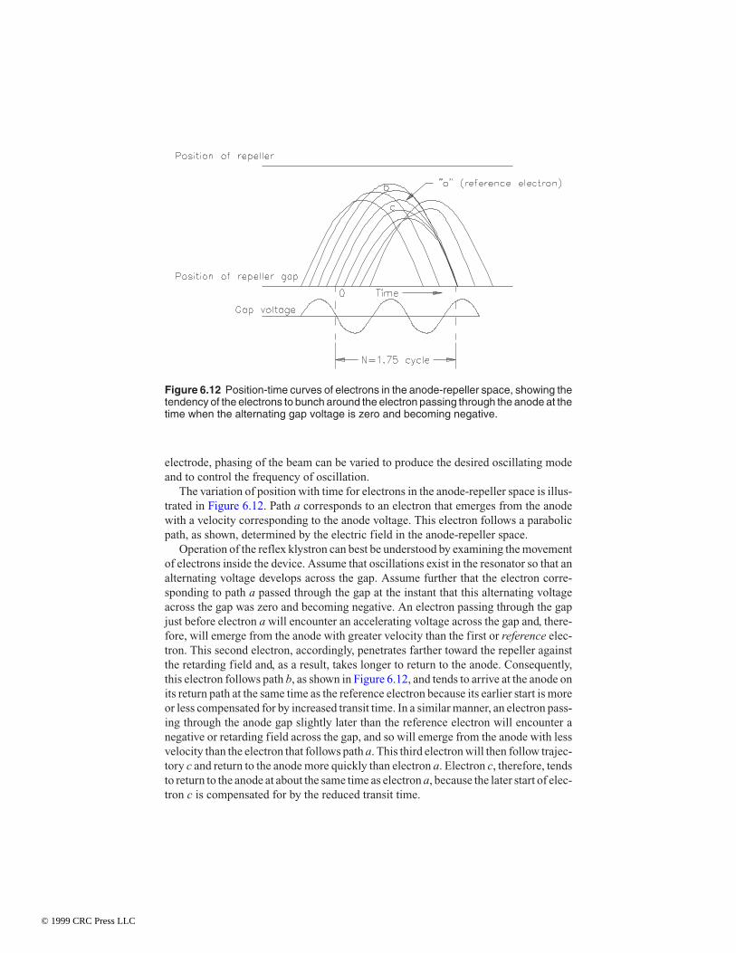
electrode, phasing of the beam can be varied to produce the desired oscillating modeand to control the frequency of oscillation.
The variation of position with time for electrons in the anode-repeller space is illus-trated in Figure 6.12. Path a corresponds to an electron that emerges from the anodewith a velocity corresponding to the anode voltage. This electron follows a parabolicpath, as shown, determined by the electric field in the anode-repeller space.
Operation of the reflex klystron can best be understood by examining the movementof electrons inside the device. Assume that oscillations exist in the resonator so that analternating voltage develops across the gap. Assume further that the electron corre-sponding to path a passed through the gap at the instant that this alternating voltageacross the gap was zero and becoming negative. An electron passing through the gapjust before electron a will encounter an accelerating voltage across the gap and, there-fore, will emerge from the anode with greater velocity than the first or reference elec-tron. This second electron, accordingly, penetrates farther toward the repeller againstthe retarding field and, as a result, takes longer to return to the anode. Consequently,this electron follows path b, as shown in Figure 6.12, and tends to arrive at the anode onits return path at the same time as the reference electron because its earlier start is moreor less compensated for by increased transit time. In a similar manner, an electron pass-ing through the anode gap slightly later than the reference electron will encounter anegative or retarding field across the gap, and so will emerge from the anode with lessvelocity than the electron that follows path a. This third electron will then follow trajec-tory c and return to the anode more quickly than electron a. Electron c, therefore, tendsto return to the anode at about the same time as electron a, because the later start of elec-tron c is compensated for by the reduced transit time.
Figure 6.12 Position-time curves of electrons in the anode-repeller space, showing thetendency of the electrons to bunch around the electron passing through the anode at thetime when the alternating gap voltage is zero and becoming negative.
© 1999 CRC Press LLC

This variation with time of the velocity of electrons emerging from the anode istermed velocity modulation. The effect of this phenomenon can be seen in Figure 6.12to cause a bunching of electrons about the electron that passed through the gap when theresonator voltage was zero and becoming negative. This bunching causes the electronsthat are returned toward the anode by the repeller to pass through the anode gap inbursts or pulses, one each cycle. When these pulses pass through the gap at such a timethat the electrons in the pulse are slowed as a result of the alternating voltage existingacross the gap at the instant of their return passage, energy will be delivered to the oscil-lations in the resonator, thereby assisting in maintaining the oscillations. This conditioncorresponds to a transit time N from the resonator toward the repeller and back to theresonator of approximately:
N n= + 34 (6.1)
Where:n = an integer (including zero)
The transit time in the anode-repeller space in any particular case depends upon thefollowing:
• The anode voltage
• Repeller voltage
• Geometry of the anode-repeller space
The extent of the bunching action that takes place when the transit time of the refer-ence electron has the correct value for sustaining oscillations is determined by the fol-lowing:
• The amplitude of the alternating voltage across the resonator gap in relation to theanode and repeller voltage
• The geometry of the repeller space
The reflex klystron typically includes a grid to concentrate the electric field so that itmay efficiently couple to the electron beam. Such a device is illustrated in Figure 6.13.
The reflex klystron may be used as a local oscillator, low-power FM transmitter, ortest signal source. Reflex tubes are used primarily from 4 to 40 GHz. Power outputs of 1W or less are common.
The reflex tube is the only klystron in which beam feedback is used to produce out-put energy. In klystrons with more than one cavity, the electron beam passes througheach cavity in succession.
6.3.2 The Two-Cavity Klystron
The two-cavity klystron operates on the same bunching principle as the reflex kly-stron, but incorporates two cavities connected by a drift tube. Figure 6.14 shows across section of a classic device. The heater/cathode element (shown as A in the fig-
© 1999 CRC Press LLC

ure) produces an electron beam in conjunction with a focusing electrode. The routetaken by the electrons is as follows:
• The beam passes through grid elements D in the side of a reentrant cavity resona-tor (the buncher).
• The beam then passes through the drift tube, which is at the same electrical poten-tial as the buncher.
• Finally, the beam enters a second resonator termed the collector, which is pro-vided with a grid E.
The cathode and its associated focusing electrode are maintained at a high negativepotential with respect to the remaining part of the structure, all of which is at the samedc potential. The entire arrangement illustrated in the figure is enclosed in a vacuum.
The operational principles of the two-cavity klystron are similar in nature to those ofthe reflex klystron. Assume, first, that oscillations exist in the buncher so that an alter-nating voltage is present across the gap D. When this voltage is zero but just becomingpositive, an electron passing through the buncher travels through the grids D, down thedrift tube, and into the collector resonator with unchanged velocity. However, an elec-tron that passes through the buncher slightly later receives acceleration while passingthrough, because of the positive alternating field that it encounters between grids D,and enters the drift tube with increased velocity. This later electron, therefore, tends toovertake the earlier electron. Similarly, an electron that arrives at the buncher slightly
Figure 6.13 Schematic cross section of a reflex klystron oscillator.
© 1999 CRC Press LLC

earlier than the first (reference electron) encounters a field between grids D that op-poses its motion. Hence, this early electron enters the drift tube with reduced velocityand tends to drop back and be overtaken by the reference electron.
As a result of these actions, the electrons bunch together as they travel down the drifttube. This effect is more pronounced at certain distances from the buncher. If the col-lector is located at a distance where the bunching is pronounced, the electrons enter theelement in pulses, one pulse per cycle.
With proper adjustment, the amount of power required to produce the bunching ef-fect is relatively small compared with the amount of energy delivered by the electronbeam to the collector. As a result, the klystron operates as an amplifying device.
The Two-Cavity Klystron Oscillator
The two-cavity klystron oscillator is designed for applications requiring moderatepower (up to 100 W), stable frequency output, and low sideband noise. The device hasa coupling iris on the wall between the two cavities. The tube can be frequency-modu-lated by varying the cathode voltage about the center of the oscillating mode. Al-though it is more efficient and powerful than the reflex klystron, the two-cavity kly-
Figure 6.14 Cross section of a classic two-cavity klystron oscillator.
© 1999 CRC Press LLC

stron requires more modulator power. The two-cavity klystron typically is used inDoppler radar systems.
The Two-Cavity Klystron Amplifier
Similar in design to the two-cavity oscillator, the two-cavity klystron amplifier pro-vides limited power output (10 W or less) and moderate gain (about 10 dB). A drivingsignal is coupled into the input cavity, which produces velocity modulation of thebeam. After the drift space, the density-modulated beam induces current in the outputresonator. Electrostatic focusing of the beam is common.
The two-cavity klystron finds only limited applications because of its restrictions onoutput power and gain. For many applications, solid-state amplifiers are a better choice.
6.3.3 The Multicavity Klystron
The multicavity klystron is an important device for amplifying signals to high powerlevels at microwave frequencies [3]. Each cavity tuned to the operating frequencyadds about 20 dB gain to the 10 dB gain offered by the basic two-cavity klystron am-plifier. Overall gains of 60 dB are practical. Cavities may be tuned to either side ofresonance to broaden the operating bandwidth of the device. Klystrons with up toeight cavities have been produced. Operating power for continuous wave klystronsranges up to 1 MW per device, and as much as 50 MW per device for pulsed applica-tions.
The primary physical advantage of the klystron over a grid-based power tube is thatthe cathode-to-collector structure is virtually independent of transit-time effects.Therefore, the cathode can be made large and the electron beam density kept low.
The operating frequency of a klystron may be fixed—determined by the mechanicalcharacteristics of the tube and its cavities—or tunable. Cavities are tuned mechanicallyusing one of several methods, depending on the operating power and frequency. Tuningis accomplished by changing the physical dimensions of the cavities using one or moreof the following techniques:
• Cavity wall deformation, in which one wall of the cavity consists of a thin dia-phragm that is moved in and out by a tuning mechanism. About 3 percent fre-quency shift may be accomplished using this method, which varies the induc-tance of the cavity.
• Movable cavity wall, in which one wall of the cavity is moved in or out by a tuningmechanism. About 10 percent frequency shift is possible with this approach,which varies the inductance of the cavity.
• Paddle element, in which an element inside the cavity moves perpendicularly tothe beam and adds capacitance across the interaction gap. A tuning range of about25 percent is provided by this approach.
• Combined inductive-capacitive tuning, which uses a combination of the previousmethods. Tuning variations of 35 percent are possible.
© 1999 CRC Press LLC

Each of these tuning methods may be used whether the cavity is inside or outside thevacuum envelope of the tube. Generally speaking, however, tubes that use externalcavities provide more adjustment range, usually on the order of 35 percent. Band-width may be increased by stagger tuning of the cavities, at the expense of gain.
High conversion efficiency requires the formation of electron bunches, which oc-cupy a small region in velocity space, and the formation of interbunch regions with lowelectron density. The latter is particularly important because these electrons are phasedto be accelerated into the collector at the expense of the RF field. Studies show that theenergy loss as a result of an electron accelerated into the collector may exceed the en-ergy delivered to the field by an equal but properly phased electron. Therein lies a key inimproving the efficiency of the klystron: Recover a portion of this wasted energy.
Klystrons are cooled by air or liquid for powers up to 5 kW. Tubes operating in ex-cess of 5 kW are usually water- or vapor-cooled.
Operating Principles
A high-velocity electron beam emitted from the cathode passes through the anode andinto the RF interaction region, as shown in Figure 6.15 [3]. An external magnetic fieldis employed to prevent the beam from spreading as it passes through the tube. At theother end of the device, the electron beam impinges on the collector electrode, whichdissipates the beam energy and returns the electron current to the beam power supply.
Figure 6.15 Principal elements of a klystron.
© 1999 CRC Press LLC

The RF interaction region, where amplification occurs, contains resonant cavitiesand field-free drift spaces. The first resonant cavity encountered by an electron in thebeam (the input cavity) is excited by the microwave signal to be amplified, and an alter-nating voltage of the signal frequency is developed across the gap. This action can bebest explained by drawing an analogy between a resonant cavity and a conventionalparallel resonant LC circuit (see Figure 6.16). The cavity gap corresponds to the capaci-tor, and the volume of the cavity to the inductor. If the cavity is of the correct physicaldimensions, it will resonate at the desired microwave frequency. At resonance, oppositesides of the gap become alternately positive and negative at a frequency equal to the mi-crowave input signal frequency.
An electron passing through the gap when the voltage across the gap is zero contin-ues with unchanged velocity along the drift tube toward the next cavity gap; this elec-tron is the reference electron. An electron passing through the same gap slightly later isaccelerated by the positive field at the gap. This electron speeds up and tends to over-take the reference electron ahead of it in the drift tube. However, an electron that passesthrough the gap slightly ahead of the reference electron encounters a negative field andis slowed down. This electron tends to fall back toward the following reference elec-tron. As a result of passing the alternating field of the input-cavity gap, the electronsgradually bunch together as they travel down the drift tube, as illustrated in Figure 6.17.Because electrons approach the input-cavity gap with equal velocities and emerge withdifferent velocities, which are a function of the microwave signal, the electron beam issaid to be velocity-modulated. As the electrons travel down the drift tube, bunching de-velops, and the density of electrons passing a given point varies cyclically with time.This bunching is identical in nature to the action in a two-cavity klystron, discussed inSection 6.3.2.
The modulation component of the beam current induces current in each of the fol-lowing cavities. Because each cavity is tuned near resonance, the resulting increase infield at each gap produces successively better-defined electron bunches and, conse-quently, amplification of the input signal. The RF energy produced in this interactionwith the beam is extracted from the beam and fed into a coaxial or waveguide transmis-sion line by means of a coupling loop in the output cavity. The dc beam input power notconverted to RF energy is dissipated in the collector.
Figure 6.16 Klystron cavity: (a) physical arrangement, (b) equivalent circuit.
(a) (b)
© 1999 CRC Press LLC

Emission
The electron gun section of a klystron, shown in Figure 6.18, consists of the followingelements [3]:
• A heater
• An emitter
• A beam-forming focusing electrode
• A modulating anode
When the emitter temperature is raised to the proper value by the heater, electrons arereleased from the emitter surface. The electrons are accelerated toward the modulat-ing anode, which is at a positive potential with respect to the emitter. As the electronstravel between the emitter and the modulating anode, they are formed into a beam bythe lens action of the focusing electrode and modulating anode. Figure 6.19 showshow this lens is formed.
All cathodes have a specific optimum range of operating temperature. The tempera-ture of the cathode must be sufficiently high to prevent variations in heater power fromaffecting the electron emission current (beam current) in the klystron. However, thetemperature of the emitting surface must not be higher than necessary because exces-sive temperature can shorten emission life. Figure 6.20 shows beam current (emissioncurrent) as a function of the emitter temperature, which varies directly with heaterpower. When the heater voltage (Ef1) is too low, the emitter will not be hot enough to
Figure 6.17 Bunching effect of a multicavity klystron.
© 1999 CRC Press LLC

produce the desired beam current. In addition, even small variations in heater voltagewill change the beam current significantly. With the proper heater voltage (Ef2), con-stant beam current will be maintained even with minor variations in heater voltage. Thesame is true for a higher heater voltage value (Ef3), but in this case the emitter tempera-ture is greater than that needed for the desired beam current. Reduced tube life will re-
Figure 6.18 Diode section of a klystron electron gun.
Figure 6.19 Beam forming in the diode section of a klystron electron gun.
© 1999 CRC Press LLC

sult. The correct value of heater voltage and/or heater current is included in the datashipped with each klystron.
Modulating Anode
Because the modulating anode is electrically isolated from both the cathode and kly-stron body (the RF structure, between polepieces) the voltage applied to it provides aconvenient means for controlling beam current independently of the beam voltage ap-plied between the cathode and body, as shown in Figure 6.21. When the cathode is op-erated in the space-charge-limited region, Ef2 and Ef3 of Figure 6.20, the emission cur-rent will be a specific function of the applied voltage:
I k Eb = 32 (6.2)
Where:Ib = beam current in ampsE = beam potential in volts
The constant k is a function of the geometry of the cathode-anode structure, and istermed perveance. Because the modulating anode is physically positioned betweenthe RF structure (body) and the cathode, even if the full beam voltage is maintainedbetween cathode and body, the actual beam current into the tube may be reduced atwill by biasing the modulating anode to any voltage between cathode and body. Fig-ure 6.22 shows the relationship between beam current and voltage described in theprevious equation.
Figure 6.20 Klystron beam-current variation as a function of emitter temperature.
© 1999 CRC Press LLC

Magnetic Field
Beam focusing is used in multielement klystrons to keep the electron beam uniformlysmall. Focusing may be accomplished by one or more electrostatic lenses or externalmagnetic fields placed parallel to the beam. Magnetic focusing is the most commonmethod. Permanent magnets are used at operating powers of about 5 kW or less. Elec-tromagnets are used at higher powers.
Electromagnetic coils typically are placed around the klystron to develop the mag-netic field along the axis of the RF circuit. This field controls the size of the electronbeam and keeps it aligned with the drift tubes. Figure 6.23 illustrates the beam-formingportion at the cathode end of the klystron and RF section, where the magnetic field isdeveloped between two cylindrical disks (polepieces). The electron beam in this illus-tration is shown traveling two paths. One path shows the beam spreading out to pointsA; the other path shows the beam confined by the magnetic field to a constant sizethroughout the distance between polepieces. The beam spreads toward points A whenthe magnetic field is inadequate.
Figure 6.24 shows the magnetic field pattern of a typical solenoid used for klystrons.When direct current passes through the magnetic coils, a magnetic field is generatedalong the axis of the tube. The strength of this field can be controlled by changing thecurrent flow through the magnetic coils. The shape of the field is determined bypolepiece geometry and winding distribution inside the solenoid. Figure 6.25 illus-trates the field pattern and the shape of the beam for a properly adjusted field.
Figure 6.26 demonstrates how the beam of a klystron is distorted when an externalmagnetic material is placed near the RF circuit of the tube. Electrons in the beam willfollow the bent magnetic field lines and may strike the walls of the drift tube. Klystrondamage can result. Magnetic materials such as screwdrivers, wrenches, bolts, and nutsmust not be left near the magnetic circuit or near the cathode or collector. Magnetictools must not be used to tune a klystron.
Figure 6.21 Modulating-anode electrode in a multicavity klystron.
© 1999 CRC Press LLC

Figure 6.23 The effect of a magnetic field on the electron beam of a klystron.
Figure 6.22 Beam-current variation as a function of modulating-anode voltage.
© 1999 CRC Press LLC

RF Structure
The RF structure of a klystron amplifier consists of tunable resonant circuits (cavi-ties) positioned along the axis of the electron beam. The electron beam travelingthrough the cavities provides the necessary coupling between each of the RF circuits.
The cavities of a klystron are high-frequency parallel resonant circuits constructedso that they provide an RF voltage across the capacitive component (gap), which inter-acts with the dc beam. Figure 6.27a illustrates the polarity near the drift-tube tips withina cavity excited by an alternating voltage of microwave signal frequency. Figure 6.27b
Figure 6.24 Field pattern of a klystron electromagnet.
Figure 6.25 Field pattern and beam shape in a properly adjusted magnetic field.
© 1999 CRC Press LLC

is the equivalent circuit of a simple cavity. To achieve circuit resonance, the inductiveand capacitive reactances of each of the components must be equal. The reactance ofeach of the components shown in the figure can be measured separately. However, thereactances of the components within a klystron cavity are difficult to determine, be-cause they cannot be measured individually. Therefore, the regions of voltage maximaor minima are used to define each component of a klystron cavity in the following way:
• The capacitance of a cavity is developed across the gap at the drift tubes where thevoltage is at maximum.
• The inductance of a cavity is located in the outer volume of the cavity where thevoltage is at minimum.
Figure 6.26 Distortion of the field pattern and beam shape due to magnetic material inthe magnetic field.
Figure 6.27 Klystron cavity: (a) physical element, (b) equivalent electric circuit.
(a) (b)
© 1999 CRC Press LLC

By defining each component of a cavity in these terms, it is easy to visualize changesin the volume as changes in inductance, and changes affecting the gap as changes incapacitance.
The resonant frequency of each cavity can be adjusted to the operating frequency ofthe RF generator. This can be accomplished in one of two ways:
• Change the inductance by changing the volume of the cavity.
• Change the capacitance of the drift-tube gaps.
Figure 6.28 illustrates how the capacitance of the cavity gap can be modified by at-taching a post to a thin-wall diaphragm with a paddle close to the drift-tube gap. In (a),the mechanical configuration of a cavity with this type of tuning is illustrated; (b)shows the equivalent circuit capacitance formed between the paddle and the drift tubesat the gap. Moving the paddle away from the drift tubes decreases the gap capacitanceand increases the resonant frequency of the cavity.
Figure 6.29 shows a schematic diagram of the equivalent circuits of a four-cavityklystron. Circuit 1 is the input, and circuit 4 is the output. Figure 6.30a illustrates mag-netic-loop coupling, where the RF energy is fed through a coaxial line with its centerconductor inserted into the klystron cavity. The end of the center conductor is formedinto a loop. This forms a simple one-turn transformer that couples RF energy into or outof the cavity through a coaxial transmission line. Figure 6.30b shows the equivalent cir-cuit. The transformer formed by the loop and cavity is an impedance-matching devicebetween the transmission line and the cavity.
Klystron cavities may be externally loaded to improve their instantaneous band-width characteristics. These loads lower the Q of the cavities slightly and thereby in-crease the bandwidth of the klystron.
Figure 6.28 Capacitance-tuned klystron cavity: (a) physical element, (b) equivalent cir-cuit.
(a) (b)
© 1999 CRC Press LLC

Phased Electron Operation
By properly phasing the second-harmonic fields of a klystron, a favorable electrondensity distribution pattern can be established at the output gap. The result is the gen-eration of additional RF energy.
A phase-space diagram for a high-power klystron is shown in Figure 6.31. Thecurves represent a plot of the relative phase of the reference electrons as a function ofaxial distance along the tube. Electrons having negative slope have been decelerated.Electrons having positive slope have been accelerated with respect to a nonacceleratedelectron parallel to the axis. The diagram shows how the electrons are nicely grouped atthe output cavity gap while the interbunch regions are relatively free of electrons.
This interaction can be viewed another way, as shown in Figure 6.32, which plots thenormalized RF beam currents as a function of distance along the tube. The curves showthat the fundamental component of the plasma wave has a negative slope at the thirdgap. This normally would be a poor condition, but because of the drift of the interbunch
Figure 6.29 Schematic equivalent circuit of a four-cavity klystron.
Figure 6.30 Klystron loop coupling: (a) mechanical arrangement, (b) equivalent electriccircuit.
(a) (b)
© 1999 CRC Press LLC

electrons, the fundamental current peaks at nearly 1.8 times the dc beam current. Thetheoretical limit for perfect bunching in a delta function is 2. The second harmonic ofthe plasma wave also peaks at the output gap, which adds to the conversion efficiency.
Types of Devices
Klystrons can be classified according to the following basic parameters:
Figure 6.31 Plot of the relative phase of the reference electrons as a function of axialdistance in a high-efficiency klystron.
Figure 6.32 Plot of the normalized RF beam currents as a function of distance along thelength of a high-efficiency klystron.
© 1999 CRC Press LLC

• Power operating level. Klystrons are available ranging from a few hundred wattsto more than 10 MW.
• Operating frequency. Klystrons typically are used over the frequency range of300 MHz to 40 GHz.
• Number of cavities. The number of resonant cavities may range from one to fiveor more. Furthermore, the cavities may be integral or external to the vacuum en-velope of the device.
The klystron is a true linear amplifier from zero signal level up to 2 to 3 dB belowsaturated output. Figure 6.33 shows a typical transfer characteristic for a klystron. RFmodulation is applied to the input drive signal. Amplitude modulation typically is lim-ited to the linear portion of the gain transfer characteristic (class A operation). The re-sult is low efficiency, because the beam power is always on. For applications requiringfrequency modulation, the drive power is set for saturated output.
Pulse modulation of the klystron may be obtained by applying a negative rectangularvoltage, instead of a dc voltage, to the cathode. The RF drive, set to a saturation value,usually is pulsed on for a slightly shorter time than the beam pulse.
Because of the high power levels typically used at UHF frequencies, device effi-ciency is a critical parameter. Klystrons usually are rated in terms of saturated effi-ciency, determined by dividing the saturated RF output power by the dc input power.
Saturated efficiency governs the maximum peak-of-sync efficiency available whenbeam-pulsing techniques are employed for UHF-TV service. Peak-of-sync efficiencyis the commonly used figure of merit (FOM) expression, defined as the peak-of-syncoutput power divided by the dc input power.
Figure 6.33 Typical gain, output power, and drive requirements for a klystron.
© 1999 CRC Press LLC

Table 6.1 lists typical operating parameters for an integral-cavity klystron.
6.3.4 Beam Pulsing
Beam pulsing is a common method of improving the efficiency of a broadband linearklystron amplifier. Depending on the transmitted waveform, efficiency may beboosted by 25 percent or more. This technique typically is used in UHF-TV transmit-ters to reduce visual klystron beam dissipation during video portions of the transmis-sion. Sync pulsing, as the technique is commonly known, is accomplished by chang-ing the operating point of the tube during the synchronizing interval, when peakpower is required, and returning it to a linear transfer characteristic during the videoportion of the transmission.
This control is accomplished through the application of a voltage to an electrodeplaced near the cathode of the klystron. Biasing toward cathode potential increases thebeam current, and biasing toward ground (collector potential) decreases beam current.
In the composite TV waveform, video information occupies 75 percent of the ampli-tude, and sync occupies the remaining 25 percent. The tip of sync represents the peakpower of the transmitted waveform. Black (the blanking level) represents 56 percent ofthe peak power. If the blanking level could be made to represent 100 percent modula-tion and the sync pulsed in, as in a radar system, efficiency would be increased signifi-cantly. Unfortunately, the color-burst signal extends 50 percent into the sync region,and any attempt to completely pulse the sync component would distort the color-burstreference waveform. Sync pulsing is, therefore, limited to 12.5 percent above black toprotect color-burst. Two common implementations of beam pulsing can be found:
Table 6.1 Typical Operating Parameters for an Integral-Cavity Klystron for UHF-TVService (Courtesy of Varian.)
Parameter Typical ValueOperating frequency (visual) 519 MHzOutput power, peak-of-sync 64 kWDrive power, peak-of-sync 15 WGain, peak-of-sync 36 dBEfficiency, saturated 55%Bandwidth, –1 dB 6 MHzBeam voltage 24.5 kVBeam current 4.8 ABody current 10 MA dcModulating-anode voltage 17 kV dcModulating-anode current 0.5 mA dcFocusing current 30 A dcLoad VSWR > 1.1:1Collector temperature 130°C
© 1999 CRC Press LLC

• Modulating-anode (mod-anode) pulsing
• Annular beam control electrode (ACE) pulsing
The mod-anode system (first discussed in Section 6.3.3) utilizes an additional elec-trode after the cathode to control beam power. The ACE-type tube operates on a simi-lar principle, but the annular ring is placed close to the cathode so that the ring en-closes the electron beam. Because of the physical design, pulsing with the ACE-typegun is accomplished at a much lower voltage than with a mod-anode device. The ACEelement, in effect, grid-modulates the beam.
In theory, the amount of beam-current reduction achievable and the resulting effi-ciency improvement are independent of whether mod-anode or ACE-type pulsing areused. In practice, however, differences are noted. With existing mod-anode pulsers, anefficiency improvement of about 19 percent in beam current over nonpulsed operationmay be achieved. A beam reduction of 30 to 35 percent may be achieved through use ofan ACE-equipped tube. The effect of ACE voltage on beam current is shown in Figure6.34 for an external-cavity klystron.
The ACE electrode, positioned in the gun assembly, is driven by a negative-directednarrowband video signal of a few hundred volts peak. The annular ring varies the beamdensity through a pinching action that effectively reduces the cross-sectional area ofthe stream of electrons emitted by the cathode. The klystron thus operates in aquasi-class-AB condition rather than the normal class A (for linear TV service).
A peak-of-sync FOM for an integral-cavity UHF-TV klystron without ACE orequivalent control is 0.67 to 0.68. Through the use of an ACE-type tube, the FOM maybe increased to 0.80. Similar improvements in efficiency can be realized for exter-nal-cavity klystrons. A typical switching-type mod-anode pulser is shown in Figure6.35.
Pulsing is not without its drawbacks, however. The greater the pulsing, the greaterthe precorrection required from the modulator. Precorrection is needed to compensatefor nonlinearities of the klystron transfer characteristic during the video modulation pe-riod. Level-dependent RF phase precorrection also may be required. Switching be-tween different klystron characteristics produces phase modulation of the visual car-rier. If not corrected, this phase modulation may result in intercarrier “buzz” in the re-ceived audio. These and other considerations limit the degree of pulsing that may beachieved on a reliable basis.
6.3.5 Integral vs. External Cavity
In an integral-cavity klystron, the resonant cavities are located within the vacuum en-velope of the tube. In an external-cavity klystron, the cavities are located outside theenvelope in a mechanical assembly that wraps around the drift tube.
Fundamentally, klystron theory applies equally to integral- and external-cavitytubes. In both cases, a velocity-modulated electron beam interacts with multiple reso-nant cavities to provide an amplified output signal. The resonant cavity interaction gapand drift length requirements for optimum performance—including conversion effi-ciency—are independent of whether the tuning mechanism is inside or outside the vac-
© 1999 CRC Press LLC

Figure 6.35 Block diagram of a switching mod-anode pulser.
Figure 6.34 Klystron beam current as a function of annular control electrode voltage.
© 1999 CRC Press LLC

uum envelope. High-efficiency integral- and external-cavity klystrons have been de-signed to provide maximum conversion performance consistent with signal bandwidthrequirements. The saturated conversion efficiency is essentially identical for integral-or external-cavity klystrons with equal numbers of resonant cavities.
Number of Cavities
The relative benefits of integral- vs. external-cavity klystrons can be debated atlength. Discussion typically centers on operating efficiency, life expectancy, and re-placement device cost. In a comparison of the efficiency of integral- vs. external-cav-ity klystrons for UHF-TV applications, however, the question really boils down to thenumber of cavities (four or five) used in the device. Four-cavity external tubes arestandard. It is usually not practical to produce high-power five-cavity external tubesfor mechanical and electrical (voltage standoff) reasons.
Integral devices permit the addition of a fifth cavity to the design for two primaryreasons. First, the device itself is mechanically more robust. The addition of a fifth cav-ity to an external klystron increases the length and weight of the device. Because of thesize of the drift tube in an external device designed for UHF-TV frequencies, the addi-tional weight is difficult to support. Second, because the cavities are enclosed in a vac-uum in the integral design, voltage standoff problems are greatly reduced.
The tuning mechanism of an integral-cavity klystron is enclosed in a rigid steelshell. In the external-cavity unit, the tuning mechanism is in air. Within the region of thetuning mechanism, RF fields can reach high levels, especially at the high end of theUHF-TV band. The highest energy field occurs in the area of the last cavity. Because ofthe high dielectric properties of a vacuum, dielectric breakdown is less of a problem inthe integral design, which places the tuning mechanism within a vacuum envelope.This situation is of particular concern at the high end of the UHF band, where the spac-ing of tuning elements is closer.
Four-cavity integral-type klystrons are manufactured, but for power outputs of 30kW or less. The 60 kW integral klystron, typically used for UHF-TV broadcasting, isproduced as a five-cavity design.
The physics of the integral- and external-cavity klystrons are essentially the same. Ina comparison of integral and external units of like design—that is, with the same num-ber of cavities—performance should be identical. The two units follow the same lawsof physics and use basically the same components up to the beam stick. It is when man-ufacturers take advantage of the relative merits of each design that differences in per-formance are realized.
Efficiency
For the sake of comparison, the data presented in this section will assume:
• The power level is 60 kW
• All integral-cavity devices utilize five cavities
• All external-cavity devices utilize four cavities
© 1999 CRC Press LLC

The five-cavity integral S-tuned klystron is inherently at least 20 percent more effi-cient than a four-cavity tube. (S-tuning refers to the method of stagger tuning the cavi-ties.) The five-cavity klystron generally is specified by the manufacturer for a mini-mum efficiency of 52 percent (saturated efficiency). Typical efficiency is 55 percent.Four-cavity devices are characteristically specified at 42 percent minimum and 45 per-cent typical.
This efficiency advantage is possible because the fifth cavity of the integral designpermits tuning patterns that allow maximum transfer of RF energy while maintainingadequate bandpass response. Tighter bunching of electrons in the beam stick, a func-tion of the number of cavities, also contributes to the higher efficiency operation. In ac-tuality, the fifth cavity allows design engineers to trade gain for efficiency. Still, thefive-cavity tube has significantly more gain than the four-cavity device. The five-cav-ity unit, therefore, requires less drive, which simplifies the driving circuit. A five-cav-ity klystron requires approximately 25 W of drive power, while a four-cavity tube needsas much as 90 W for the same power output.
Under pulsed operation, approximately the same reduction in beam current is real-ized with both integral- and external-cavity klystrons. In a comparison of peak-of-syncFOM, the efficiency differences will track. There is, fundamentally, no reason that onetype of klystron should pulse differently than the other.
Performance Tradeoffs
It is the designer’s choice whether to build a transmitter with the klystron cavities lo-cated inside or outside the vacuum envelope. There are benefits and drawbacks toeach approach.
When the cavity resonators are a part of the tube, the device becomes more compli-cated and more expensive. However, the power generating system is all together in onepackage, which simplifies installation significantly.
When the resonator is separate from the tube, as in an external-cavity device, it canbe made with more compliance (greater room for adjustment). Consequently, a singledevice may be used over a wider range of operating frequencies. In terms of UHF-TV, asingle external-cavity device may be tuned for operation over the entire UHF-TV band.This feature is not possible if the resonant cavities are built into the device. To cover theentire UHF-TV band, three integral-cavity tubes are required. The operational divi-sions are:
• Channels 14 to 29 (470 to 566 MHz)
• Channels 30 to 51 (566 to 698 MHz)
• Channels 52 to 69 (698 to 746 MHz)
This practical limitation to integral-cavity klystron construction may be a drawbackfor some facilities. For example, it is not uncommon for group operations to share oneor more spare klystrons. If the facilities have operating frequencies outside the limits ofa single integral device, it may be necessary to purchase more than one spare. Also,
© 1999 CRC Press LLC

when the cavities are external, the resonators are in air and can be accessed to permitfine adjustments of the tuning stages for peak efficiency.
The advantages of tube changing are significant with an integral device. Typicaltube change time for an integral klystron is 1 hour, as opposed to 4 to 6 hours for an ex-ternal device. The level of experience of the technician is also more critical when an ex-ternal-type device is being changed. Tuning procedures must be carefully followed bymaintenance personnel to avoid premature device failure.
6.3.6 MSDC Klystron
Developmental work on the multistage depressed collector (MSDC) klystron began inthe mid-1980s. The project1 produced a working tube capable of efficiency in UHFservice that had been impossible with previous klystron-based technology.
The MSDC device may be used in a number of varied applications. NASA originallybecame involved in the project as a way to improve the efficiency of satellite transmit-ters. With limited power available onboard a space vehicle, efficient operation is criti-cally important. Such transmitters traditionally operate in a linear, inefficient mode.UHF-TV broadcasters were interested in the MSDC because it promised to reduce thehuge operating costs associated with high-power operation.
Experimentation with depressed collector klystrons dates back to at least the early1960s. Early products offered a moderate improvement in efficiency, but at the price ofgreater mechanical and electrical complexity. The MSDC design, although mechani-cally complex, offers a significant gain in efficiency.
Theory of Operation
MSDC tubes have been built around both integral-cavity and external-cavity kly-strons. The devices are essentially identical to a standard klystron, except for the col-lector assembly. Mathematical models provided researchers with detailed informationon the interactions of electrons in the collector region. Computer modeling also pro-vided the basis for optimization of a beam-reconditioning scheme incorporated intothe device. Beam reconditioning is achieved by including a transition region betweenthe RF interaction circuit and the collector under the influence of a magnetic field. Itis interesting to note that the mathematical models made for the MSDC project trans-lated well into practice when the actual device was constructed.
From the electrical standpoint, the more stages of a multistage depressed collectorklystron, the better. The tradeoff, predictably, is increased complexity and, therefore,increased cost for the product. There is also a point of diminishing returns that isreached as additional stages are added to the depressed collector system. A four-stagedevice was chosen for TV service because of these factors. As more stages are added(beyond four), the resulting improvement in efficiency is proportionally smaller.
1 A joint effort of the National Aeronautics and Space Administration (NASA), severalUHF-TV transmitter manufacturers, Varian Associates, and other concerns.
© 1999 CRC Press LLC

Figure 6.36 shows the mechanical configuration of the four-stage MSDC klystron.Note the “V” shape that was found, through computer modeling, to provide the bestcapture performance, minimizing electron feedback. A partially assembled collectorassembly is shown in Figure 6.37.
Because the MSDC device is identical to a conventional klystron except for the col-lector, efficiency improvement techniques used for klystrons can be incorporated intothe MSDC. ACE-type pulsing commonly is used to improve efficiency in TV applica-tions. Figure 6.38 illustrates the effects of ACE voltage on beam current.
Electron Trajectories
The dispersion of electrons in the multistage collector is the key element in recoveringpower from the beam and returning it to the power supply. This is the mechanism thatpermits greater operating efficiency from the MSDC device.
Figure 6.39 illustrates the dispersion of electrons in the collector region during a car-rier-only operating mode. Note that there is little dispersion of electrons between stagesof the MSDC. Most are attracted to electrode 4, the element at the lowest potential(6.125 kV), referenced to the cathode.
Figure 6.36 Mechanical design of the multistage depressed collector assembly. Notethe “V” shape of the 4-element system.
© 1999 CRC Press LLC

Figure 6.40 shows collector electron trajectories at 25 percent saturation. The elec-trons exhibit predictable dispersion characteristics during the application of modula-tion, which varies the velocity of the electrons. This waveform is a reasonable approxi-mation of average modulation for a typical video image.
Figure 6.37 A partially assembled MSDC collector. (Courtesy of Varian.)
Figure 6.38 Beam current as a function of annular control electrode voltage for anMSDC klystron.
© 1999 CRC Press LLC

Figure 6.41 shows electron trajectories at 50 percent saturation, approximately theblanking level. Note the increased number of electrons attracted to electrodes 2 and 3,the higher-potential electrodes (referenced to the cathode).
Figure 6.42 illustrates electron dispersion at 90 percent saturation, approximatelythe level of sync in a video waveform. As the modulation level is increased, more elec-trons are attracted to the higher-voltage electrodes. The dramatic increase in electroncapture by electrode 1, the highest-potential element of the device (at a voltage of 24.5kV, referenced to the cathode), can be observed.
The electrons, thus, sort themselves out in a predictable manner. Notice the arc thatis present on many electron traces. The electrons penetrate the electrostatic field of thecollector, then are pulled back to their respective potentials.
A savings in power is realized because the electrostatic forces set up in the MSDCdevice slow down the electrons before they contact the copper collector electrode. Theheat that would be produced in the collector is, instead, returned to the power supply in
Figure 6.39 Collector electron trajectories for the carrier-only condition. Note thatnearly all electrons travel to the last electrode (4), producing electrode current I4.
Figure 6.40 Collector trajectories at 25 percent saturation. With the application of mod-ulation, the electrons begin to sort themselves out.
© 1999 CRC Press LLC

the form of electric energy. In theory, peak efficiency would occur if the electrons wereslowed down to zero velocity. In practice, however, that is not possible.
Figure 6.43 shows the distribution of collector current as a function of drive power.With no RF drive, essentially all current goes to electrode 4, but as drive is increased, I4
drops rapidly as collector current is distributed among the other elements. Note that thecurrent to electrode 5 (cathode potential) peaks at about 10 percent of beam current.This suggests that the secondary yield of the collector surfaces is within acceptable lim-its.
Inserted between the klystron and the collector assembly is a refocusing electromag-net that controls the electron beam as it enters the collector region.
Figure 6.41 Collector electron trajectories at 50 percent saturation, approximately theblanking level. The last three electrodes (2, 3, and 4) share electrons in a predictablemanner, producing currents I2, I3, and I4.
Figure 6.42 Collector trajectories at 90 percent saturation, the sync level. Note the sig-nificant increase in the number of electrons attracted to the first electrode, producing I1.
© 1999 CRC Press LLC

Mechanical Construction
The completed MSDC assembly is shown in Figure 6.44 with the collector shield par-tially removed to allow visibility of the collector elements. The collector of thefour-stage MSDC design actually is composed of five elements mounted between ce-ramic rings for electrical insulation. The fifth electrode is at cathode potential.
Cooling for the MSDC is, not surprisingly, more complicated than for a conven-tional klystron. The tradeoff, however, is that there is less heat to remove because of thehigher efficiency of the device. Water cooling is provided on each electrode of theMSDC tube.
Figure 6.45 illustrates the overall mechanical design of an external-cavity version ofthe MSDC tube, including placement of the device in its cavity bay.
Although the MSDC has not been in service for a sufficient length of time to com-pletely characterize the product life expectancy, researchers believe that the MSDC de-sign will have little, if any, effect on the lifetime of the klystron. The electron beam is es-sentially unchanged. The tube is identical to a conventional integral- or external-cavityklystron except in collector assembly.
Figure 6.43 The distribution of electrode current as a function of drive power. Note thesignificant drop in I4 as drive power is increased. I5 is the electrode at cathode potential.
© 1999 CRC Press LLC

MSDC Power Supply
Design criteria for the collector power supply system provide a mixed bag of require-ments. The critical parameter is the degree of regulation between the cathode and an-ode. The relative differences between the elements of the collector are not, in most ap-plications, significant. Consequently, the bulk of the power supplied to the tube doesnot need to be well regulated. This is in contrast with conventional klystron operation,
Figure 6.44 The MSDC collector assembly withthe protective shield partially removed. (Courtesyof Varian.)
Figure 6.45 Mechanical construction of an external-cavity MSDC tube: (a) device, (b)device in cavity assembly.
(a) (b)
© 1999 CRC Press LLC

in which the entire beam power supply must be regulated. This factor effectively de-creases the amount of power that must be regulated to 1 to 2 percent of the dc input,offsetting to some extent the additional cost involved in constructing multiple sup-plies to facilitate the 4-stage MSDC design. Two approaches can be taken to collectorpower supply design:
• Parallel arrangement, shown in Figure 6.46
• Series arrangement, shown in Figure 6.47
Note that, in both cases, the collector electrodes are stepped at a 6.125 kV potentialdifference for each element.
Device Performance
The efficiency improvement of the MSDC klystron over the conventional klystron isimpressive. For TV applications, the MSDC—in pulsed operation—is more thantwice as efficient as a conventional klystron.
The bandpass performance of the device is another critical parameter. Figure 6.48charts power output as a function of frequency and RF drive at full power. (Drive poweris charted from 0.5 to 16 W.) Figure 6.49 charts power output as a function of frequency
Figure 6.46 Parallel configuration of the MSDC power supply. Each supply section hasan output voltage that is an integral multiple of 6.125 kV.
© 1999 CRC Press LLC

and RF drive with the tube in a beam-pulsing mode. (Drive power is charted from 0.5 to32 W.) Note that the traces provide good linearity over a 6 MHz bandwidth. Gain, as afunction of frequency and power, is essentially constant and undisturbed.
Table 6.2 lists typical operating parameters for an external-cavity MSDC device.
Applying the MSDC Klystron
A block diagram of a typical system is shown in Figure 6.50. The 60 kW TV transmit-ter incorporates two external-cavity MSDC klystrons, one for the visual and anotherfor the aural. Design of the transmitter is basically identical to a non-MSDC system,with the exception of the power supply and cooling system. The efficiency availablefrom the MSDC makes further device improvements subject to the law of diminishingreturns, as mentioned previously. Support equipment begins to consume an increas-ingly large share of the power budget as the output device efficiency is improved.Tuning of the MSDC klystron is the same as for a conventional klystron, and the samemagnetic circuit is typically used.
The power supply arrangement for the example MSDC system is shown in Figure6.51. A series beam supply was chosen for technical and economic reasons. Althoughthe current to each collector varies widely with instantaneous output level, the total cur-rent stays within narrow limits. Using a single transformer for all supplies, therefore,minimizes the size of the iron core required. A 12-pulse rectifier bank provides low rip-
Figure 6.47 Series configuration of the MSDC power supply, which uses four identical6.125 kV power supplies connected in series to achieve the needed voltages.
© 1999 CRC Press LLC

Figure 6.48 Device bandwidth as a function of frequency and drive power. Beam volt-age is 24.5 kV, and beam current is 5.04 A for an output power of 64 kW. These tracesrepresent the full-power test of the MSDC device.
Figure 6.49 Device bandwidth in the beam-pulsing mode as a function of frequencyand drive power. Beam voltage is 24.5 kV, and beam current is 3.56 A with an outputpower of 34.8 kW.
© 1999 CRC Press LLC

ple and reduces the need for additional filtering. The size and complexity of the recti-fier stack are increased little beyond a normal beam supply because the total potentialof the four supplies is similar to that of a normal klystron transmitter (24.5 to 27.5 kV).
The collector stages of the MSDC device are water-cooled by a single water paththat loops through each electrode element. Because high voltage is present on the indi-vidual elements, purity of the water is critical to proper operation. A two-stage systemis used with a water-to-water plate heat exchanger separating the primary and second-ary systems.
6.4 Klystrode/Inductive Output Tube (IOT)The Klystrode tube is the result of a development program started in 19802 withUHF-TV in mind as a primary application. The basic concept of the Klystrode datesback to the late 1930s,3 but it was not until the early 1980s that serious engineering ef-fort was put into the tube to make it a viable product for high-power UHF service. Thefundamental advantage of the Klystrode, also known as the inductive output tube
Table 6.2 Typical Operating Parameters for an External-Cavity MSDC Klystron forUHF-TV service (Courtesy of Varian.)
Parameter Typical ValueOperating frequency (visual) 519 MHzOutput power, peak-of-sync 64 kWDrive power, peak-of-sync 20 WGain, peak-of-sync 35 dBFigure of merit 1.31
Bandwidth, –1 dB 6 MHzBeam voltage 24.5 kVBeam current 5.3 ABody current 50 mA dcModulating-anode voltage 19.5 kV dcModulating-anode current 0.5 mA dcFocusing current 11 A dcIon pump voltage 3.2 kV dcLoad VSWR > 1.1:1Refocusing coil current 7 A dcRefocusing coil voltage 10 V dc
1 Figure of merit is equal to the quotient of peak-of-sync output power and the average dc beaminput power.
2 Varian/Eimac3 Andrew Haeff, 1938
© 1999 CRC Press LLC

Figure 6.51 Simplified schematic diagram of the power supply for an MSDC klystrontransmitter. A single high-voltage transformer with multiple taps is used to provide theneeded collector voltage potentials.
Figure 6.50 Simplified block diagram of a 60 kW (TVT) MSDC transmitter. The auralklystron may utilize a conventional or MSDC tube at the discretion of the user.
© 1999 CRC Press LLC

(IOT), is its ability to operate class B. The result is higher efficiency when comparedwith a conventional klystron.
6.4.1 Theory of Operation
As its name implies, the Klystrode tube is a hybrid between a klystron and a tetrode.The high reliability and power-handling capability of the klystron is due, in part, tothe fact that electron beam dissipation takes place in the collector electrode, quite sep-arate from the RF circuitry. The electron dissipation in a tetrode is at the anode andthe screen grid, both of which are an inherent part of the RF circuit and, therefore,must be physically small at UHF frequencies. The tetrode, however, has the advantagethat modulation is produced directly at the cathode by a grid so that a long drift spaceis not required to produce density modulation. The Klystrode/IOT has a similar ad-vantage over the klystron—high efficiency in a small package [4]. The Klystrode tubeis a registered trademark of Varian. The IOT is the generic description for the device,and it will be used in this discussion.
The IOT is shown schematically in Figure 6.52. The electron beam is formed at thecathode, density-modulated with the input RF signals by a grid, then acceleratedthrough the anode aperture. In its bunched form, the beam drifts through a field-free re-gion, then interacts with the RF field in the output cavity. Power is extracted from thebeam in the same way as in a klystron. The input circuit resembles that of a typical UHFpower grid tube. The output circuit and collector resemble those in a klystron.
A production version of a 60 kW device is shown in Figure 6.53. Double-tuned cavi-ties are used to obtain the required operating bandwidth. The load is coupled at the sec-ond cavity, as shown in Figure 6.54. This arrangement has proved to be an attractiveway to couple power out of the device because no coupling loop or probe is required inthe primary cavity, which can be a problem at the high end of the UHF band.
Because the IOT provides both beam power variation during sync pulses (as in apulsed klystron) and variation of beam power over the active modulating waveform, it iscapable of high efficiency. The device provides full-time beam modulation as a resultof its inherent structure and class B operation.
6.4.2 Electron Gun
Many design elements from the klystron have been borrowed for use in the IOT [4]. Abarium aluminate cathode is used for the gun, taken from a conventional klystron to-gether with its heater structure. The methods used to support the cathode, heater, andnecessary heat shields in the klystron gun have been retained for use in the IOT. Fig-ure 6.55 shows the construction of the IOT gun and output cavity.
In the IOT, the RF input voltage is applied between the cathode and a grid that allowsextra electrons to be drawn from the cathode into a low-quiescent-current electronbeam according to the instantaneous RF voltage appearing between the grid and cath-ode. The resulting density-modulated beam is then passed into the klystron-like RFoutput interaction region of the tube.
© 1999 CRC Press LLC

The grid is clamped in place in front of the cathode, supported on a metal cylinder,and isolated from the cathode by a ceramic insulator. A second ceramic insulator sup-ports the complete gridded electron gun at the correct distance from the grounded an-
Figure 6.53 A 60 kW Klystrode tube mounted inits support stand with the output cavity attached.(Courtesy of Varian.)
Figure 6.52 Simplified schematic diagram of the Klystrode tube.
© 1999 CRC Press LLC

ode. This ceramic insulator completes the vacuum envelope and holds off the full beamvoltage of approximately 30 kV. The IOT gun operates at cathode-to-anode voltages ap-proximately 50 percent higher than those of conventional klystron guns. Stray capaci-tance in the grid support structure has been minimized to reduce losses.
The grid-to-cathode space of the electron gun forms the end of a long and complexRF transmission line from the RF input connector of the input cavity system. This de-sign has a significant effect upon the final frequency range of the IOT input cavity. Be-cause the grid-to-cathode distance is crucial to the physics of the device, the grid re-quires a rigid support structure to maintain proper spacing at high operating tempera-tures.
6.4.3 Grid Structure
A pyrolytic graphite grid is used in the IOT because of its strength and its ability tomaintain desired specifications at elevated temperatures [4]. Pyrolytic graphite has aunique advantage over other common grid materials in that its strength increases asthe temperature climbs to 2500°C and above, whereas the strength of pure metals uni-versally decreases as the temperature increases. This allows the designer to produce athin grid, with fine grid wires that may be accurately positioned and will retain theirposition and shape when raised to operating temperatures of approximately 1000°C.
During production of the grid, a hydrocarbon, typically methane, is fed into alow-pressure chamber containing a graphite rod of the correct form to produce the re-quired graphite shell. A shell typically consists of a graphite cylinder with a closed,shaped end. The cold gas is passed into a hot zone in the reactor, which is heated by anRF eddy current system from outside the vessel. An ordered carbon structure, as op-posed to an amorphous structure, is required. To provide the needed processing, thetemperature of the reactor is set to approximately 2000°C at a pressure of 10 torr. Thegraphite shells produced in this way have a layered structure with anisotropic propertiesand are physically durable.
Figure 6.54 A close-up view of thedouble-tuned output cavity of a 60 kWKlystrode tube. (Courtesy of Varian.)
© 1999 CRC Press LLC

The shells are then machined to the desired shape and size, and holes are cut into theresulting grid back using a laser under computer control. The process of producing apyrolytic graphite grid is illustrated in Figure 6.56.
6.4.4 Input Cavity
Although similar, the Klystrode and the IOT are not identical. There are both subtleand significant differences in each design. The greatest departure can be seen in theconfiguration of the input cavity [4]. The design of the IOT is shown in Figure 6.57. Acylindrical resonant cavity containing an annular sliding tuning door is used. The cav-ity is folded at the IOT electron gun end to make contact with the tube via an RFchoke structure. Because both the cathode and grid operate at beam potential (30 kV),it is necessary to maintain the body of the cavity and its tuning mechanism at ground
Figure 6.55 Overall structure of the IOT gun and output cavity. (After [4].)
© 1999 CRC Press LLC

potential by using RF chokes to prevent leakage of RF energy, while holding off thefull beam voltage.
At a given point on the grid connection within the RF choke, an insulated high-volt-age cable is attached and exits so that the –30 kV dc can be supplied to the grid. This ca-ble is screened and fitted with RF chokes to prevent UHF energy from passing into thebeam power supply. RF input energy is fed via a coaxial cable to the input cavity, whichis excited by means of a loop antenna carried by the annular tuning door.
Cooling air for the IOT electron gun and grid connection is fed through an insulatedair pipe down the inside of the input cavity.
The tuning door of the cavity is driven by three two-stage tuning screws coupled tothe outside via a rubber-toothed belt and bevel-gear drive. A mechanical turns-counteris provided to relate cavity door position with operating frequency.
6.4.5 Output Cavity
The primary output cavity is clamped around the output ceramic of the IOT, as on aconventional klystron [4]. The output cavity, shown in Figure 6.58, contains an RFcoupling loop that may be rotated about a horizontal axis to adjust the degree of cou-pling through a short transmission line section into a secondary cavity via a door-knob-type antenna. The secondary cavity contains a dome structure adjusted in sizeso that the cavity can be made to cover the required frequency band. An output cou-pler, of standard klystron design incorporating a loop antenna, connects the secondarycavity of the RF output feeder system via a standard output interface. This design pro-vides for instantaneous bandwidths of 8 MHz or greater.
Because RF voltages on the order of the IOT beam voltage can be expected in theoutput system, RF arc detectors are fitted into both cavities.
Cooling of the output cavities is accomplished by means of filtered forced air. Airenters the primary cavity, passes over the output ceramic and coupling loop, then exits
Figure 6.56 Pyrolytic graphite grid: (a) shell, (b) grid blank, (c) grid cut.
(a) (b)
(c)
© 1999 CRC Press LLC

via holes in the coupling hub assembly into the secondary cavity. After cooling the sec-ondary cavity, some of the air exits via the contact fingers on the tuning doors, while asmall portion traverses the output loop and coupler, exiting at a stub-pipe fitting for thatpurpose.
Typical operating parameters for the IOT are shown in Table 6.3.
6.4.6 Application Considerations
An active crowbar circuit is included in most applications of the Klystrode/IOT toprotect the pyrolytic graphite grid in the event of an arc condition inside the tube [4].The crowbar provides the added benefit of reducing the amount of gas generated inthe tube during an arc. A block diagram of a typical crowbar is shown in Figure 6.59.The response time of the crowbar is typically less than 10 µs. The peak current per-missible through the discharge tube may be 3000 A or greater.
Because of the IOT’s class B operation, the response of the power supply to a vary-ing load is an important design parameter. If a standard klystron beam supply were usedin an IOT-equipped RF generator, performance under varying modulation levels could
Figure 6.57 IOT input cavity. (After [4].)
© 1999 CRC Press LLC

be unacceptable. Consider the application of a bounce (black-to-white) signal to a TVtransmitter. Beam current for a typical IOT 60 kW transmitter would change from ap-proximately 400 mA to 2 A. The effect with a conventional klystron supply would beringing of about 20 percent on the beam voltage. The IOT power supply, therefore, mustbe designed for tight transient regulation.
Table 6.3 Typical Operating Parameters of the IOT in TV Service
Parameter Typical ValueBeam voltage 28 kVMean beam current 1.15 APeak beam current 2.50 AGrid bias –72 VGrid current 1 mABody current 6 mAInput power 399 WOutput power 40.3 kW
Figure 6.58 IOT output cavity. (After [4].)
© 1999 CRC Press LLC

The IOT does not have the same hard saturation characteristic as a klystron. TheIOT’s high-power transfer curve flattens more slowly than a klystron’s and continues toincrease with increasing drive power, requiring a different approach to linearity correc-tion.
6.4.7 Continuing Research Efforts
Several variations on the basic Klystrode/IOT theme have been developed, includingair-cooled devices operating at 30 kW and above. Air cooling is practical at thesepower levels because of the improved efficiency that class B operation provides.
Research also is being conducted to extend the operating power of the IOT to 500kW or more. Designed for scientific research applications, such devices offer numer-ous benefits over conventional klystron technology. The IOT is much smaller than aklystron of similar power, and it requires less support circuitry. Because of the im-proved efficiency, power supply requirements are reduced, and device cooling is sim-plified.
Figure 6.59 Simplified block diagram of the crowbar circuit designed into the KlystrodeSK-series (Comark) transmitters. The circuit is intended to protect the tube from poten-tially damaging fault currents.
© 1999 CRC Press LLC

6.5 Constant Efficiency AmplifierBecause of the similarity between the spent electron beam in an IOT and that of a kly-stron or traveling-wave tube, it is possible to consider the use of a multistage de-pressed collector on an IOT to improve the operating efficiency [5]. This had beenconsidered by Priest and Shrader [6] and by Gilmore [7], but the idea was rejected be-cause of the complexity of the multistage depressed collector assembly and becausethe IOT already exhibited fairly high efficiency. Subsequent development by Symons[5, 8] has led to a prototype device (at this writing). An inductive output tube, modi-fied by the addition of a multistage depressed collector, has the interesting property ofproviding linear amplification with (approximately) constant efficiency.
6.5.1 Theory of Operation
Figure 6.60 shows a schematic representation of the constant efficiency amplifier(CEA) [5]. The cathode, control grid, anode and output gap, and external circuitry areessentially identical with those of the IOT amplifier. Drive power introduced into theinput cavity produces an electric field between the control grid and cathode, whichdraws current from the cathode during positive half-cycles of the input RF signal. For
Figure 6.60 Schematic overview of the MSDC IOT or constant efficiency amplifier. (Af-ter [5].)
© 1999 CRC Press LLC

operation as a linear amplifier, the peak value of the current—or more accurately, thefundamental component of the current—is made (as nearly as possible) proportionalto the square root of the drive power, so that the product of this current and the voltageit induces in the output cavity will be proportional to the drive power.
Following the output cavity is a multistage depressed collector in which several typi-cal electron trajectories are shown. These are identified by the letters a through e. Thecollector electrodes are connected to progressively lower potentials between the anodepotential and the cathode potential so that more energetic electrons penetrate moredeeply into the collector structure and are gathered on electrodes of progressively lowerpotentials.
In considering the difference between an MSDC IOT and an MSDC klystron, it isimportant to recognize that in a class B device, no current flows during the portion ofthe RF cycle when the grid voltage is below cutoff and the output gap fields are acceler-ating. As a result, it is not necessary to have any collector electrode at a potential equalto or below cathode potential. At low output powers, when the RF output gap voltage isjust equal to the difference in potential between the lowest-potential collector electrodeand the cathode, all the current will flow to that electrode. Full class B efficiency is thusachieved under these conditions.
As the RF output gap voltage increases with increased drive power, some electronswill have lost enough energy to the gap fields so they cannot reach the lowest potentialcollector, and so current to the next-to-the-lowest potential electrode will start increas-ing. The efficiency will drop slightly and then start increasing again until all the currentis just barely collected by the two lowest-potential collectors, and so forth.
Maximum output power is reached when the current delivered to the output gap issufficient to build up an electric field or voltage that will just stop a few electrons. Atthis output power, the current is divided between all of the collector electrodes and theefficiency will be somewhat higher than the efficiency of a single collector, class B am-plifier. Computer simulations have demonstrated that it is possible to select the collec-tor voltages so as to achieve very nearly constant efficiency from the MSDC IOT deviceover a wide range of output powers [5].
The challenge of developing a multistage depressed collector for an IOT is not quitethe same as that of developing a collector for a conventional klystron [8]. It is differentbecause the dc component of beam current rises and falls in proportion to the squareroot of the output power of the tube. The dc beam current is not constant as it is in a kly-stron (or a traveling-wave tube for that matter). As a result, the energy spread is low be-cause the output cavity RF voltage is low at the same time that the RF and dc beam cur-rents are low. Thus, there will be small space-charge forces, and the beam will notspread as much as it travels deep into the collector toward electrodes having the lowestpotential. For this reason, the collector is likely to be rather long and thin when com-pared to the multistage depressed collector for a conventional klystron, as describedpreviously.
Figure 6.61 charts the calculated efficiency for an IOT with six depressed collectorstages, set at 0.1, 0.2, 0.3, 0.45, 0.7, and 1.0 times the beam voltage (compared to that ofa conventional IOT).
© 1999 CRC Press LLC

6.6 Traveling Wave TubeThe traveling wave tube (TWT) is a linear-beam device finding extensive applicationsin communications and research. Power levels range from a few watts to 10 MW. Gainranges from 40 to 70 dB for small drive signals. The TWT consists of four basic ele-ments:
• Electron gun. The gun forms a high-current-density beam of electrons that inter-act with a wave traveling along the RF circuit to increase the amplitude of the RFsignal. In a typical application, electrons are emitted from a cathode and con-verged to the proper beam size by focusing electrodes.
• RF interaction circuit. The RF wave is increased in amplitude as a result of inter-action with the electron beam from the gun. The fundamental principle on whichthe TWT operates is that an electron beam, moving at approximately the same ve-locity as an RF wave traveling along a circuit, gives up energy to the RF wave.
• Magnetic electron beam focusing system. The beam size is maintained at theproper dimensions through the interaction structure by the focusing system. Thismay be accomplished by using either a permanent magnet or an electromagneticfocusing element.
• Collector. The electron beam is received at the collector after it has passedthrough the interaction structure. The remaining beam energy is dissipated in thecollector.
Figure 6.61 Calculated efficiency of an MSDC IOT compared to an unmodified IOT.(After [5].)
© 1999 CRC Press LLC

Figure 6.62 shows the basic elements of a TWT.The primary differences between types of TWT devices involve the RF interaction
structure employed. In Figure 6.62, the interaction structure is a helix. A variety ofother structures may be employed, depending on the operating power and frequency.Three common approaches are used to provide the needed magnetic beam focusing. Il-lustrated in Figure 6.63, they are:
• Electromagnetic focusing, used primarily on high-power tubes, where tight beamfocusing is required.
• Permanent-magnet focusing, used where the interaction structure is short.
• Periodic permanent-magnet focusing, used on most helix TWT and coupled-cav-ity tubes. The magnets are arranged with alternate polarity in successive cellsalong the interaction region.
6.6.1 Theory of Operation
The interaction structure acts to slow the RF signal so that it travels at approximatelythe same speed as the electron beam. Electrons enter the structure during both posi-tive and negative portions of the RF cycle. Electrons entering during the positive por-tion are accelerated; those entering during the negative portion are decelerated. Theresult is the creation of electron bunches that produce an alternating current superim-posed on the dc beam current. This alternating current induces the growth of an RFcircuit wave that encourages even tighter electron bunching.
One or more severs are included to absorb reflected power that travels in a backwarddirection on the interaction circuit. This reflected power is the result of a mismatch be-tween the output port and the load. Without the sever, regenerative oscillations couldoccur.
Figure 6.62 Basic elements of a traveling wave tube.
© 1999 CRC Press LLC

At a given frequency, a particular level of drive power will result in maximumbunching and power output. This operating point is referred to as saturation.
Interaction Circuit
The key to TWT operation lies in the interaction element. Because RF waves travel atthe speed of light, a method must be provided to slow down the forward progress ofthe wave to approximately the same velocity as the electron beam from the cathode.The beam speed of a TWT is typically 10 to 50 percent the speed of light, correspond-ing to cathode voltages of 4 to 120 kV. Two mechanical structures commonly are usedto slow the RF wave:
• Helix circuit. The helix is used where bandwidths of an octave or more are re-quired. Over this range the velocity of the signal carried by the helix is basicallyconstant with frequency. Typical operating frequencies range from 500 MHz to40 GHz. Operating power, however, is limited to a few hundred watts. TWTs in-tended for higher-frequency operation may use a variation of the helix, shown inFigure 6.64. The ring-loop and ring-bar designs permit peak powers of hundredsof kilowatts. The average power, however, is about the same as that of a conven-tional helix because the structure used to support the interaction circuit is thesame.
Figure 6.63 Magnetic focusing for a TWT: (a) solenoid-type, (b) perma-nent-magnet-type, (c) periodic permanent-magnet structure.
(a) (b)
(c)
© 1999 CRC Press LLC

• Coupled-cavity circuit. The coupled-cavity interaction structure permits opera-tion at high peak and average power levels, and moderate bandwidth (10 percentbeing typical). TWTs using coupled-cavity structures are available at operatingfrequencies from 2 to 100 GHz. The basic design of a coupled-cavity interactioncircuit is shown in Figure 6.65. Resonant cavities, coupled through slots cut in thecavity end walls, resemble a folded waveguide. Two basic schemes are used: thecloverleaf and the single-slot space harmonic circuit.
The cloverleaf, also known as the forward fundamental circuit, is used primarily onhigh-power tubes. The cloverleaf provides operation at up to 3 MW peak power and 5kW average at S-band frequencies. The single-slot space harmonic interaction circuit ismore common than the cloverleaf. The mechanical design is simple, as shown in thefigure. The single-slot space harmonic structure typically provides peak power of up to50 kW and average power of 5 kW at X-band frequencies.
Pulse Modulation
The electron beam from the gun may be pulse-modulated using one of four methods:
• Cathode pulsing. The cathode is pulsed in a negative direction with respect to thegrounded anode. This approach requires the full beam voltage and current to beswitched.
• Anode pulsing. This approach is similar to cathode pulsing, except that the fullbeam voltage is switched between cathode potential and ground. The currentswitched, however, is only that value intercepted on the anode. Typically, the in-tercepted current is a few percent of the full beam potential.
Figure 6.64 Helix structures for a TWT: (a) ring-loop circuit, (b) ring-bar circuit.
(a)
(b)
© 1999 CRC Press LLC

• Focus electrode pulsing. If the focus electrode, which normally operates at ornear cathode potential, is biased negatively with respect to the cathode, the beamwill be turned off. The voltage swing required is typically one-third of the fullcathode voltage. This approach is attractive because the focus electrode draws es-sentially no current, making implementation of a switching modulator relativelyeasy.
• Grid pulsing. The addition of a grid to the cathode region permits control of beamintensity. The voltage swing required for the grid, placed directly in front of thecathode, is typically 5 percent of the full beam potential.
Electron Gun
The electron gun of a TWT is a device that supplies the electron beam to the tube [9].A schematic diagram of a generic electron gun is given in Figure 6.66. The deviceconsists of a hot cathode heated by an electric heater, a negatively biased focusingelectrode or focuser, and a positively biased accelerating anode. The cross-sectionalview given in the figure can be a two-dimensional or three-dimensional coaxial struc-ture [10, 11].
An axially symmetrical solid cylindrical electron beam is produced by the gun struc-ture shown in Figure 6.66 if the structure is axially cylindrically symmetrical. If themiddle of the hot cathode is made nonemitting and only the edge of the cathode is emit-ting, the cathode becomes an annular cathode [9]. The annular cathode produces a hol-low beam. The annular electron beam can be used to reduce beam current for a givenmicrowave output power.
If the gun structure shown in Figure 6.66 is two dimensional, then a ribbon-shapedelectron beam is produced. A ribbon-shaped beam is used for a TWT of a two-dimen-sional structure.
Figure 6.65 Coupled-cavity interaction structures: (a) forward fundamental circuit or“cloverleaf,” (b) single-slot space harmonic circuit.
(a) (b)
© 1999 CRC Press LLC

If the angle of the focusing electrode against the axis of the electron beam is 67.5°and the anode is also tilted forward to produce a rectilinear flow (electron flow parallelto the z axis in Figure 6.66), then such an electron gun is termed the Pierce gun.
In practice, the hot cathode surface is curved as shown in Figure 6.67 to increase theelectron emitting surface and to obtain a high-density electron beam.
Beam Focusing
Electrons in an electron beam mutually repel each other by the electron’s own cou-lomb force because of their negative charge [9]. In addition, the electron beam usuallyexists in proximity to the positively biased slow-wave structure, as shown in Figure6.68. Therefore, the electron beam tends to diverge. The process of confining theelectron beam within the desired trajectory against the mutual repulsion and diverg-ing force from the slow-wave structure is termed electron beam focusing.
The electron beam in a TWT is usually focused by a dc magnetic flux applied paral-lel to the direction of the electron beam, which is coaxial to the slow-wave transmissionline. Variations on this basic technique include:
• Brillouin flow, where the output of the electron gun is not exposed to the focusingmagnetic flux [12].
• Immersed flow, where the electron gun itself is exposed to and unshielded fromthe focusing para-axial longitudinal magnetic flux [12].
• Generic flow, where the electron gun is not shielded from the focusing magneticflux, and focusing flux is not para-axia. (In other words, neither Brillouin nor im-mersed flow.)
Collector Assembly
Various configurations are used for the collector assembly of a TWT. Figure 6.69shows a selection of the more common, including [9]:
Figure 6.66 Generic TWT electron gunstructure. (From [9]. Used with permis-sion.)
© 1999 CRC Press LLC

• Plate collector
• Cone collector
• Curved cone
• Cylinder collector
• Depressed potential cylinder
• Two-stage collector
• Three-stage collector
Cooling options include conduction, air, and water.
Figure 6.68 Generic configuration of a traveling wave tube. (From [9]. Used with per-mission.)
Figure 6.67 Cross-sectional view of a TWTelectron gun with a curved hot cathode.(From [9]. Used with permission.)
© 1999 CRC Press LLC

Cooling of a low-power TWT is accomplished by clamping the tube to a metal base-plate, mounted in turn on an air- or liquid-cooled heat sink. Coupled-cavity tubes below1 kW average power are convection-cooled by circulating air over the entire length ofthe device. Higher-power coupled-cavity tubes are cooled by circulating liquid over thetube body and collector.
6.6.2 Operating Efficiency
Efficiency is not one of the TWT’s strong points. Early traveling wave tubes offeredonly about 10 percent dc-to-RF efficiency. Wide bandwidth and power output arewhere the TWT shines. TWT efficiency may be increased in two basic ways: (1) col-lector depression for a single-stage collector, or (2) use of a multistage collector.
Collector depression refers to the practice of operating the collector at a voltagelower than the full beam voltage. This introduces a potential difference between the in-teraction structure and the collector, through which electrons pass. The amount bywhich a single-stage collector can be depressed is limited by the remaining energy ofthe slowest electrons. In other words, the potential reduction can be no greater than theamount of energy of the slowest electrons, or they will turn around and reenter the inter-action structure, causing oscillations.
By introducing multiple depressed collector stages, still greater efficiency can berealized. This method provides for the collection of the slowest electrons at one collec-tor potential, while allowing those with more energy to be collected on other stages thatare depressed still further. This approach, similar to the MSDC design discussed previ-ously, is illustrated in Figure 6.70.
Figure 6.69 Cross-sectional view of various collector configurations for a TWT. (From[9]. Used with permission.)
© 1999 CRC Press LLC

6.6.3 Operational Considerations
Although traveling wave tubes offer numerous benefits to the end user, they are notwithout their drawbacks.
Intermodulation Distortion
TWTs are susceptible to intermodulation (IM) distortion when multiple carriers areintroduced, as in double illuminated or multiple SCPC (single channel per carrier)satellite transponders. These IM products may be found at frequencies that are dis-placed from the fundamental carriers by the difference in frequency between them.When multiple carriers are present, the potential for IM exists. This potential is re-duced by operating the TWT below saturation. Power must be reduced (backed off) inproportion to the number of carriers and their relative power.
Second-Harmonic Content
Because of the wide bandwidth and nonlinear operating characteristics under satura-tion conditions, a TWT may generate significant second-harmonic energy. It is notuncommon to measure second-harmonic energy at the output of a TWT that is downonly 10 dB from the operating carrier.
Figure 6.70 Power supply configuration for a multistage depressed collector TWT.
© 1999 CRC Press LLC
Reduction of harmonic content usually involves injecting a coherent harmonic sig-nal with controlled phase and amplitude along with the fundamental carrier so that theyinteract, minimizing harmonic energy at the output of the device.
AM/PM Conversion
AM/PM conversion is the change in phase angle between the input and output signalsas the input varies in amplitude. The root cause of this distortion in a TWT centers onthe reduction of electron beam velocity as the input signal level increases. This causesa greater energy exchange between the electron beam and the RF wave. At a level 20dB below the input power required for saturation, AM/PM conversion is negligible.At higher levels, AM/PM distortion may increase.
Phase Variation
When the velocity of the electron beam in the TWT is changed, the phase of the out-put signal also will vary. The primary causes of beam velocity variations includechanges in one or more of the following:
• Cathode temperature
• Grid voltage
• Anode voltage
• Cathode voltage
The TWT power supply must be well regulated (to less than 0.2 percent) to preventbeam velocity changes that may result in output signal phase variations.
6.7 Crossed-Field TubesA crossed-field microwave tube is a device that converts dc into microwave energyusing an electronic energy-conversion process. These devices differ from beam tubesin that they are potential-energy converters, rather than kinetic-energy converters.The term crossed field is derived from the orthogonal characteristics of the dc electricfield supplied by the power source and the magnetic field required for beam focusingin the interaction region. This magnetic field typically is supplied by a perma-nent-magnet structure. Such devices also are referred to as M-tubes.
Practical devices based on the crossed-field principles fall into two broad catego-ries:
• Injected-beam crossed-field tubes. The electron stream is produced by an elec-tron gun located external to the interaction region, similar to a TWT. The conceptis illustrated in Figure 6.71.
• Emitting-sole tubes. The electron current for interaction is produced directlywithin the interaction region by secondary electron emissions, which result whensome electrons are driven to the negative electrode and allowed to strike it. The
© 1999 CRC Press LLC

negative electrode is formed using a material capable of producing significantnumbers of secondary-emission electrons. The concept is illustrated in Figure6.72.
6.7.1 Magnetron
The magnetron encompasses a class of devices finding a wide variety of applications.Pulsed magnetrons have been developed that cover frequency ranges from the lowUHF band to 100 GHz. Peak power from a few kilowatts to several megawatts hasbeen obtained. Typical overall efficiencies of 30 to 40 percent may be realized, de-pending on the power level and operating frequency. CW magnetrons also have beendeveloped, with power levels of a few hundred watts in a tunable tube, and up to 25kW or more in a fixed-frequency device. Efficiencies range from 30 percent to asmuch as 70 percent.
The magnetron operates electrically as a simple diode. Pulsed modulation is ob-tained by applying a negative rectangular voltage waveform to the cathode with the an-ode at ground potential. Operating voltages are less critical than for beam tubes;line-type modulators often are used to supply pulsed electric power. The physical struc-ture of a conventional magnetron is shown in Figure 6.73.
High-power pulsed magnetrons are used primarily in radar systems. Low-powerpulsed devices find applications as beacons. Tunable CW magnetrons are used in ECM(electronic countermeasures) applications. Fixed-frequency devices are used as micro-wave heating sources.
Figure 6.71 Linear injected-beam microwave tube.
© 1999 CRC Press LLC

Tuning of conventional magnetrons is accomplished by moving capacitive tuners orby inserting symmetrical arrays of plungers into the inductive portions of the device.Tuner motion is produced by a mechanical connection through flexible bellows in thevacuum wall. Tuning ranges of 10 to 12 percent of bandwidth are possible for pulsedtubes, and as much as 20 percent for CW tubes.
Operating Principles
Most magnetrons are built around a cavity structure of the type shown in Figure 6.74.The device consists of a cylindrical cathode and anode, with cavities in the anode thatopen into the cathode-anode space—the interaction space—as shown. Power can becoupled out of the cavities by means of a loop or a tapered waveguide.
Cavities, together with the spaces at the ends of the anode block, form the resonantsystem that determines the frequency of the generated oscillations. The actual shape ofthe cavity is not particularly important, and various types are used, as illustrated in Fig-ure 6.75. The oscillations associated with the cavities are of such a nature that alternat-ing magnetic flux lines pass through the cavities parallel to the cathode axis, while thealternating electric fields are confined largely to the region where the cavities open intothe interaction space. The most important factors determining the resonant frequencyof the system are the dimensions and shape of the cavities in a plane perpendicular tothe axis of the cathode. Frequency also is affected by other factors such as the end spaceand the axial length of the anode block, but to a lesser degree.
Figure 6.72 Reentrant emitting-sole crossed-field amplifier tube.
© 1999 CRC Press LLC

Figure 6.73 Conventional magnetron structure.
(a) (b)
Figure 6.74 Cavity magnetron oscillator: (a) cutaway view, (b) cross section view per-pendicular to the axis of the cathode.
© 1999 CRC Press LLC
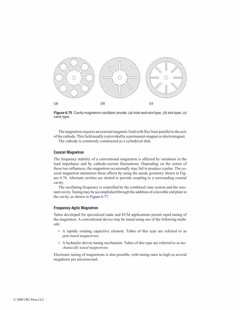
The magnetron requires an external magnetic field with flux lines parallel to the axisof the cathode. This field usually is provided by a permanent-magnet or electromagnet.
The cathode is commonly constructed as a cylindrical disk.
Coaxial Magnetron
The frequency stability of a conventional magnetron is affected by variations in theload impedance and by cathode-current fluctuations. Depending on the extent ofthese two influences, the magnetron occasionally may fail to produce a pulse. The co-axial magnetron minimizes these effects by using the anode geometry shown in Fig-ure 6.76. Alternate cavities are slotted to provide coupling to a surrounding coaxialcavity.
The oscillating frequency is controlled by the combined vane system and the reso-nant cavity. Tuning may be accomplished through the addition of a movable end plate inthe cavity, as shown in Figure 6.77.
Frequency-Agile Magnetron
Tubes developed for specialized radar and ECM applications permit rapid tuning ofthe magnetron. A conventional device may be tuned using one of the following meth-ods:
• A rapidly rotating capacitive element. Tubes of this type are referred to asspin-tuned magnetrons.
• A hydraulic-driven tuning mechanism. Tubes of this type are referred to as me-chanically tuned magnetrons.
Electronic tuning of magnetrons is also possible, with tuning rates as high as severalmegahertz per microsecond.
(a) (b) (c)
Figure 6.75 Cavity magnetron oscillator anode: (a) hole-and-slot type, (b) slot type, (c)vane type.
© 1999 CRC Press LLC

Figure 6.76 Structure of a coaxial magnetron.
Figure 6.77 Structure of a tunable coaxial magnetron.
© 1999 CRC Press LLC

Linear Magnetron
Although the most common types of magnetrons are radial in nature, the linear mag-netron and inverted magnetron may also be used, depending upon the application[13]. A cross-sectional view of a linear magnetron is given in Figure 6.78. Shown inthe figure is the O-type linear magnetron, in which the electron beam emitted fromthe electron gun is focused by a longitudinally applied dc magnetic flux density (B),as in the case of the traveling wave tube.
As shown in the figure, a number of slots are included in the basic structure. Theseslots are cut 1/4-wavelength deep, functioning as quarter-wave cavity resonators. Thisstructure forms a series of microwave cavity resonators coupling to an electron beam,in a similar manner to the multicavity klystron. The velocity modulated electrons arebunched, and the tightly bunched electrons produce amplified microwave energy at theoutput cavity, which is coupled to an external circuit. The linear magnetron typically of-fers high gain, but narrow frequency bandwidth.
6.7.2 Backward Wave Oscillator
In a traveling wave tube, if the microwave signal to be amplified is propagating in theslow-wave structure backwardly to the direction of the electron beam, the device istermed a backward wave oscillator (BWO) [13]. Microwaves traveling in a backwarddirection carry positive feedback energy toward the electron gun and yield strongervelocity modulation and bunching. Thus, the system is inherently an oscillator ratherthan a stable amplifier. The input is typically terminated by an impedance-matchedreflectionless termination device. The oscillation frequency is a function of the speedof the electrons and the time constant of the feedback mechanism. The speed of elec-tron motion is controlled by the anode voltage.
An M-type radial BWO is shown in Figure 6.79. The direction of electron pole mo-tion and the direction of microwave propagation along the annular reentrant type
Figure 6.78 Cross-sectional view of a linear magnetron. (From [13]. Used with permis-sion.)
© 1999 CRC Press LLC

slow-wave structure are opposite each other. It should be noted that the depths of theslits cut in the inner surface of the anode is very shallow—much less than 1/4-wave-length deep. In other words, the slits are not in resonance; they are not cavity resonators,as is the case of a magnetron. Rather, the slits are nonresonating, as in the case of aTWT. In the M-type radial BWO, the electron beam is focused by a magnetic flux den-sity applied perpendicular to the beam, as seen from Figure 6.79.
An M-type radial BWO is sometimes termed the Carcinotron, a trade name. A keyfeature of the Carcinotron is its wide voltage tunability over a broad frequency range.
6.7.3 Strap-Fed Devices
A radial magnetron can be configured so that every other pole of the anode resonatorsare conductively tied for microwave potential equalization, as shown in Figure 6.80a[13]. These conducting tie rings are termed straps; the technique of using strap ringsis termed strapping. Strapping ensures good synchronization of microwaves in themagnetron resonators with the rotation of electron poles.
The technique of strapping is extended and modified for an M-type radial BWO, asshown in Figure 6.80b. Strapping rings tie every other pole of the radial slow-wavestructure, as in the case of a strapped radial magnetron, but the strapping rings are nolonger reentrant. Microwave energy to be amplified is fed to the strap at one end, andthe amplified output is extracted from the other end. This type of electron tube istermed a strap-fed device.
If an M-type radial BWO is strapped, usually it does not start oscillation by itself.But, if microwave energy is fed through the strap from the outside using an external mi-crowave power source to the microwave input, then the oscillation starts—and even if
Figure 6.79 Functional schematic of the M-type radial BWO. (From [13]. Used with per-mission.)
© 1999 CRC Press LLC

the exciter source is turned off, the oscillation continues. This type of M-type radialBWO is termed the platinotron [14].
In a platinotron, if the output of the tube is fed back to the input through a high-Qcavity resonator, it becomes a self-starting oscillator. The oscillation frequency is stabi-lized by the high-Q cavity resonator. This type of high-power frequency stabilizedstrapped radial BWO is termed the stabilotron [14]. The operating powers are at kilo-watt and megawatt levels.
Performance of the platinotron depends on, among other things, the design of theslow-wave structure. For example, the interdigital slow-wave structure as shown in Fig-ure 6.80 has a limited power handling capability and frequency bandwidth. Design of aslow-wave structure with greater power handling capacity and stability, with broaderfrequency bandwidth, is possible. For example, instead of an anode with an interdigitalslow-wave structure, the anode could be made of an annular open conducting duct,loaded with a number of pairs of conducting posts across the open duct. Strapping isdone at every other tip of the pairs of conducting posts. This type of strapping loads theslow-wave structure, stabilizing it and preventing oscillation. The structure of the an-ode with an annular duct and pairs of posts increases the power handling capability.This type of loaded radial BWO is termed the amplitron [14, 10]. The amplitron is capa-ble of amplifying high-power microwave signals with pulses and continuous waves. Itis used for long-range pulsed radar transmitter amplifiers and industrial microwaveheating generators. The operating power levels range from kilowatt to megawatt levels.
Figure 6.80 Strap-fed devices: (a) strapped radial magnetron, (b) nonreentrant strap-ping of a BWO. (From [13]. Used with permission.)
(a) (b)
© 1999 CRC Press LLC

6.7.4 Gyrotron
The gyrotron is a cyclotron resonance maser.4 The device includes a cathode, collec-tor, and circular waveguide of gradually varying diameter. Electrons are emitted at thecathode with small variations in speed. The electrons then are accelerated by an elec-tric field and guided by a static magnetic field through the device. The nonuniforminduction field causes the rotational speed of the electrons to increase. The linear ve-locity of the electrons, as a result, decreases. The interaction of the microwave fieldwithin the waveguide and the rotating (helical) electrons causes bunching similar tothe bunching within a klystron. A decompression zone at the end of the device per-mits decompression and collection of the electrons.
The power available from a gyrotron is 100 times greater than that possible from aclassic microwave tube at the same frequency. Power output of 100 kW is possible at100 GHz, with 30 percent efficiency. At 300 GHz, up to 1.5 kW may be realized, butwith only 6 percent efficiency.
Theory of Operation
The trajectory of an electron in an electron beam focused by a longitudinally appliedmagnetic field is a helix [13]. If the electron velocity, electron injection angle, and ap-plied longitudinal magnetic flux density are varied, then an electron beam of helicalform with different size and pitch will be formed. A coil-shaped electron beam will beproduced by adjusting the acceleration voltage, applied magnetic flux density, and theelectron injection angle to the focusing magnetic field. The coil of the electron beamcan be a simple single coil, or—depending on the adjustment of the aforementionedthree parameters—it can be an electron beam of a double coil, or a large coil made ofthin small coils. In the case of the double-coil trajectory, the large coil-shaped trajec-tory is termed the major orbit and smaller coil trajectory is termed the minor orbit.
If a single coil-shaped electron beam is launched in a waveguide, as shown in Figure6.81, then microwaves in the waveguide will interact with the helical beam. This type ofvacuum tube is termed the helical beam tube [14]. In this class of device, a single-coilhelical beam is launched into a TE10 mode rectangular waveguide. Inside the wave-guide, microwaves travel from right to left and the helical beam travels in an oppositedirection. Therefore, the microwave-electron beam interaction is of the backward wavetype. If the microwave frequency, the focusing magnetic flux density B, and the acceler-ation voltage Va are properly adjusted, this device will function as a backward wave am-plifier. Electrons in the helical beam interact with the transverse microwave electricfields and are velocity modulated at the left-hand side of the waveguide as the beam en-ters into the waveguide. The velocity modulated electrons in the helical beam arebunched as they travel toward the right. If the alternating microwave electric field syn-
4 Maser is an acronym for microwave amplification by simulated emission of radiation. Maseris a general class of microwave amplifiers based on molecular interaction withelectromagnetic radiation.
© 1999 CRC Press LLC

chronizes its period and phase with the helical motion of bunched electrons so that theelectrons always receive retardation from microwave transverse electric fields, then theelectrons lose their kinetic energy and the microwave signal gains in electric field en-ergy according to the principle of kinetic energy conservation. Thus, the amplified mi-crowave power emerges at the waveguide output at the left (because the microwavestravel backward).
In Figure 6.81, if the microwave input port and the output port are interchanged witheach other, then the system becomes a forward wave amplifier. Such a forward waveamplifier is termed a peniotron [14].
If the electron gun is modified to incorporate a side emitting cathode and the wave-guide is changed to TE11 mode oversized circular waveguide, as shown in Figure 6.82a,the gyrotron is formed. In this device, both ends of the waveguide are open and there aresufficient reflections in the waveguide for positive feedback. The gyrotron is, thus, aforward wave oscillator.
A double-coil helical beam gyrotron is shown in Figure 6.82b. The device is formedby readjusting the anode voltage and the focusing flux density so that the electron beamis made into a double helical coil (as shown in the figure), and operating the oversizedcircular waveguide in the TE01 mode. In the TE01 mode, the microwave transverse elec-tric fields exist as concentric circles. Therefore, the tangential electric fields interactwith electrons in the small coil trajectory. The alternating tangential microwave electricfields are made to synchronize with the tangential motion of electrons in the minorcoil-shaped trajectory. Thus, electron velocity modulation takes place near the cathodeand bunching takes place in the middle of the tube. Microwave kinetic energy transfertakes place as the beam approaches the right. The focusing magnetic flux density B isapplied only in the interaction region. Therefore, if the electron beam comes out of theinteraction region, it is defocused and collected by the anode waveguide (as depicted inFigure 6.82b). If the circular waveguide is operated in an oversized TE11 mode, with thedouble-coil helical beam, then the device is referred to as a tornadotron [14]. Micro-wave-electron interaction occurs between the parallel component of tangential motionof the small helical trajectory and the TE11 mode microwave electric field. If the phaseof microwave electric field decelerates bunched electrons, then the lost kinetic energyof the bunched electrons is transferred to the microwave signal and oscillation begins.
Figure 6.81 Basic structure of ahelical beam tube. (From [13].Used with permission.)
© 1999 CRC Press LLC

Gyrotron Design Variations
The gyrotron exists in a number of design variations, each optimized for a particularfeature or application [13, 15, 16].
When the gyrotron circular waveguide is split as shown in Figure 6.83, the tube istermed the gyroklystron amplifier [13]. Both waveguides resonate to the input fre-quency, and there are strong standing waves in both waveguide resonators. The inputmicrowave signal to be amplified is fed through a side opening to the input waveguideresonator. This is the buncher resonator, which functions in a manner similar to the kly-stron. The buncher resonator imparts velocity modulation to gyrating electrons in thedouble helical coil-shaped electron beam. There is a drift space between the buncherresonator and the catcher resonator at the output. While drifting electrons bunch andbunched electrons enter into the output waveguide catcher resonator, electron speed isadjusted in such a manner that electrons are decelerated by the resonating microwaveelectric field. This lost kinetic energy in bunched electrons is transformed into micro-wave energy and microwaves in the catcher resonator are, thus, amplified. The ampli-fied power appears at the output of the tube.
If the gyrotron waveguide is an unsplit one-piece waveguide that is imped-ance-matched and not resonating, as shown in Figure 6.84, the tube is termed thegyrotron traveling wave tube amplifier [13]. In this tube, the input microwaves are fedthrough an opening in the waveguide near the electron gun. Microwaves in the wave-
(a)
(b)
Figure 6.82 Functional schematic diagram of the gyrotron: (a) single coiled helicalbeam gyrotron, (b) electron trajectory of double-coil helical beam gyrotron. (From [13].Used with permission.)
© 1999 CRC Press LLC

guide are amplified gradually as they travel toward the output port by interacting withthe double-coiled helical electron beam, which is velocity-modulated and bunched.There are no significant standing waves in the waveguide. Microwaves grow graduallyin the waveguide as they travel toward the output port as a result of interaction with elec-trons.
If the electron gun of the gyrotron is moved to the side of the waveguide and micro-wave power is extracted from the waveguide opening in proximity to the electron gun,as shown in Figure 6.85, then the device is termed a gyrotron backward oscillator [13].The principle involved is similar to the backward wave oscillator, and the process of ve-locity modulation, drifting, bunching, and catching is similar to that of the klystron.Microwave energy induced in the waveguide travels in both directions, but the circuit isadjusted to emphasize the waves traveling in a backward direction. The backwardwaves become the output of the tube and, at the same time, carry the positive feedbackenergy to the electrons just emitted and to be velocity-modulated. The system, thus,goes into oscillation.
Figure 6.83 Basic structure of the gyroklystron amplifier. (From [13]. Used with permis-sion.)
Figure 6.84 Basic structure of the gyroklystron traveling wave tube amplifier. (From[13]. Used with permission.)
© 1999 CRC Press LLC

If the gyrotron waveguide is split into two again, but this time the input side wave-guide is short and the output side waveguide is long, as shown in Figure 6.86, then thetube is termed a gyrotwystron amplifier [13]. This device is a combination of thegyroklystron and gyrotron traveling wave tube amplifier, thus the name gyrotwystronamplifier. The input side waveguide resonator is the same as the input resonator wave-guide of a gyroklystron. There are strong standing waves in the input bunched-wave-guide resonator. There is no drift space between the two waveguides. The output sidewaveguide is a long impedance-matched waveguide and there is no microwave stand-ing wave in the waveguide (a traveling-wave waveguide). As microwaves travel in thewaveguide, they interact with bunched electrons and the microwaves grow as theymove toward the output port.
6.8 Other Microwave DevicesThere are a number of variations on the basic microwave devices outlined previouslyin this chapter. Some find widespread usage, others have little commercial interest.
Figure 6.85 Basic structure of the gyrotron backward oscillator. (From [13]. Used withpermission.)
Figure 6.86 Basic structure of the gyrotwystron amplifier. (From [13]. Used with permis-sion.)
© 1999 CRC Press LLC

Among the important specialty device classifications are quasiquantum devices andmodified klystrons.
6.8.1 Quasiquantum Devices
In a gyrotron, if electrons are accelerated by extremely high voltage, they become rel-ativistic [13]. That is, the mass of an electron becomes a function of the velocity as,
( )m
m
cv
=−
0
2
1
(6.3)
Where:m = the relativistic mass of an electronm0 = the static mass of an electronc = the speed of light in vacuumv = the speed of the electron in question
The energy states of electrons are specified by a set of quantum numbers, and thetransition of energy states occurs only between those numbers so described. A set ofquantum numbers specifies the high-energy orbit and low-energy orbit of an electron.
One device based on this principle is the free electron laser, or the ubitron [13]. Aschematic diagram of the device is given in Figure 6.87. A high-speed relativistic elec-tron beam is emitted from an electron gun focused by a longitudinally applied dc mag-netic flux density B and is periodically deflected by magnetic means. The repetitiousdeflections create among relativistic electrons high-energy states and low-energystates. If the high-energy electrons in the deflection waveguides are stimulated by theresonance frequency of the waveguide resonator, then the downward transition (thetransition of electrons in a high-energy state to a low-energy state) occurs. Microwaveemissions result because of the energy transitions at the stimulation frequency.
The ubitron operates at millimeter or submillimeter wave frequencies, and typicallyat high power levels.
6.8.2 Variations on the Klystron
Because the multiple cavities of a conventional klystron are difficult to fabricate atmillimeter wavelengths, variations on the basis design have been produced [13]. In-stead of using multiple cavity resonators, the cavities can instead be combined into asingle cavity. Such a design can be accomplished through the use of ladder-shapedgrids, as shown in Figure 6.88a by the dashed lines with the single cavity. This type ofklystron is referred to as the laddertron [14]. Because of the ladder structure, a stand-ing wave will exist on on the ladder line. Velocity modulation results near the electrongun and bunching begins near the middle of the electron stream. Catching is done inthe ladder structure near the collector. Because this device is a one-cavity resonator,
© 1999 CRC Press LLC

there is built-in positive feedback. Oscillation, therefore, begins in a manner similarto a reflex klystron, also a single cavity tube.
At millimeter wavelengths, a dominant mode cavity resonator becomes very smalland loses its power-handling capability. In a laddertron, however, the cavity resonator isa multiple higher-mode resonator. Therefore, the Q of the cavity is high and the size ofthe cavity resonator is reasonably large. This being the case, the laddertron can handletens of watts of power at frequency as high as 50 GHz.
The catcher of a two-cavity klystron amplifier can be replaced by the slow-wavestructure of a traveling wave tube, as shown in Figure 6.88b. This type of tube is termedthe twystron [14]. The slow-wave structure provides a broader frequency bandwidththan a regular two-cavity klystron. A microwave input signal fed into the buncher cavityresults in velocity modulation of the electron beam. Bunching occurs while the beamdrifts, and the bunched electrons induce a microwave voltage in the slow-wave struc-ture. The electron beam is focused by the use of longitudinally applied magnetic fluxdensity B.
Figure 6.87 Basic structure of the ubitron. (From [13]. Used with permission.)
Figure 6.88 Functional schematic diagrams of modified klystrons: (a) laddertron, (b)twystron. (From [13]. Used with permission.)
(a) (b)
© 1999 CRC Press LLC

Commercial twystrons typically operate at 2–6 GHz and are used in pulsed radartransmitter power amplifiers. Pulsed peak output powers range from 1 to 7 MW (pulsewidth of 10–50 µs) [10].
6.9 Microwave Tube LifeAny analysis of microwave tube life must first identify the parameters that define life.The primary wear-out mechanism in a microwave power tube is the electron gun atthe cathode. In principle, the cathode eventually will evaporate the activating materialand cease to produce the required output power. Tubes, however, rarely fail because oflow emission, but for a variety of other reasons that are usually external to the device.
Power tubes designed for microwave applications provide long life when operatedwithin their designed parameters. The point at which the device fails to produce the re-quired output power can be predicted with some accuracy, based on design data andin-service experience. Most power tubes, however, fail because of mechanisms otherthan predictable chemical reactions inside the device itself. External forces, such astransient overvoltages caused by lightning, cooling system faults, and improper tuning,more often than not lead to the failure of a microwave tube.
6.9.1 Life-Support System
Transmitter control logic usually is configured for two states of operation:
• An operational level, which requires all of the “life-support” systems to be pres-ent before the high-voltage (HV) command is enabled.
• An overload level, which removes HV when one or more fault conditions occur.
The cooling system is the primary life-support element in most RF generators. Thecooling system should be fully operational before the application of voltages to thetube. Likewise, a cool-down period usually is recommended between the removal ofbeam and filament voltages and shutdown of the cooling system.
Most microwave power tubes require a high-voltage removal time of less than 100ms after the occurrence of an overload. If the trip time is longer, damage to the devicemay result. Arc detectors often are installed in the cavities of high-power tubes to sensefault conditions and shut down the high-voltage power supply before damage can bedone to the tube. Depending on the circuit parameters, arcs can be sustaining, requiringremoval of high voltage to squelch the arc. A number of factors can cause RF arcing, in-cluding:
• Overdrive condition
• Mistuning of one or more cavities
• Poor cavity fit (applies to external types only)
• Undercoupling of the output to the load
• Lightning strike at the antenna
© 1999 CRC Press LLC

• High VSWR
Regardless of the cause, arcing can destroy internal elements or the vacuum seal ifdrive and/or high voltage are not removed quickly. A lamp usually is included witheach arc detector photocell for test purposes.
6.9.2 Protection Measures
A microwave power tube must be protected by control devices in the amplifier sys-tem. Such devices offer either visual indications or aural alarm warnings, or they ac-tuate interlocks within the system. Figure 6.89 shows a klystron amplifier and the ba-sic components associated with its operation, including metering for each of thepower supplies. Other types of microwave power devices use similar protectionschemes. Sections of coaxial transmission line, representing essential components,are shown in the figure attached to the RF input and RF output ports of the tube. Asingle magnetic coil is shown to represent any coil configuration that may exist; itsposition in the drawing is for convenience only and does not represent its true positionin the system.
Heater Supply
The heater power supply can be either ac or dc. If it is dc, the positive terminal mustbe connected to the common heater-cathode terminal and the negative terminal to thesecond heater terminal. The amount of power supplied to the heater is important be-cause it establishes the cathode operating temperature. The temperature must be highenough to provide ample electron emission, but not so high that emission life is jeop-ardized.
Because the cathode and heater are connected to the negative side of the beam sup-ply, they must be insulated to withstand the full beam potential. This dictates the use ofa filament transformer designed specifically for the specific application.
Beam Supply
The high-voltage beam supply furnishes the dc input power to the microwave device.In a klystron, the positive side of the beam supply is connected to the body and collec-tor. The negative terminal is connected to the common heater-cathode terminal. Neverconnect the negative terminal of the beam supply to the heater-only terminal becausethe beam current will then flow through the heater to the cathode and cause prematureheater failure. The voltmeter, Eb in Figure 6.89, measures the beam voltage appliedbetween the cathode and the body of the klystron.
Current meter Ic measures collector current, typically 95 percent or more of the totaldevice current. Current meter Iby measures body current. An interlock should interruptthe beam supply if the body current exceeds a specified maximum value.
The sum of the body current (Iby) and collector current (Ic) is equal to the beam cur-rent (Ib), which should stay constant as long as the beam voltage and modulating-anodevoltage are held constant.
© 1999 CRC Press LLC

Magnet Supply
Electrical connections to the dc magnet supply typically include two meters, one formeasuring current through the circuit (Im in Figure 6.89), and one for measuring volt-age (Em). When a microwave device is installed in its magnet assembly, both parame-ters should be measured and recorded for future reference. If excessive body currentor other unusual symptoms occur, this data will be valuable for system analysis.
Undercurrent protection should be provided to remove beam voltage if the magneticcircuit current falls below a preset value. The interlock also should prevent the beamvoltage from being applied if the magnetic circuit is not energized. This scheme, how-ever, will not provide protection if windings of the magnet are short-circuited.Short-circuited conditions can be determined by measuring the normal values of volt-age and current and recording them for future reference.
The body-current overload protection should actuate if the magnetic field is reducedfor any reason.
Figure 6.89 Protection and metering system for a klystron amplifier.
© 1999 CRC Press LLC

RF Circuits
In Figure 6.89, monitoring devices are shown on the RF input and output of the kly-stron. These monitors protect the device in case of a failure in the RF output circuit.Two directional couplers and a photodetector are attached to the output of the device.These components and an RF switching device on the input form a protective networkagainst output transmission line mismatch. The RF switch is activated by thephotodetector or the reflected power monitor and must be capable of removing RFdrive power from the tube in less than 10 ms (typically).
In the RF output circuit, the forward power coupler is used to measure the relativepower output of the microwave device. The reflected power coupler measures the RFenergy reflected by the output circuit components or antenna. Damaged components orforeign material in the RF line will increase the RF reflected power. The amount of re-flected power should be no more than 5 percent of the actual forward RF output powerof the tube in most applications. An interlock monitors the reflected power and removesRF drive to the device if the reflected energy reaches an unsafe level. To protect againstarcs occurring between the monitor and the output window, a photodetector is placedbetween the monitor and the window. Light from an arc will trigger the photodetector,which actuates the interlock system to remove RF drive before the window is damaged.
6.9.3 Filament Voltage Control
Extending the life of a microwave tube begins with accurate adjustment of filamentvoltage, as noted in the previous section. The filament should not be operated at a re-duced voltage in an effort to extend tube life, as in the case of the thoriated tungstengrid tube. In a microwave tube, reduced filament voltage may cause uneven emissionfrom the surface of the cathode with little or no improvement in cathode life.
Voltage should be applied to the filament for a specified warm-up period before theapplication of beam current to minimize thermal stress on the cathode/gun structure.However, voltage should not be applied to the filaments for extended periods (typically2 hours or more) if no beam voltage is present. The net rate of evaporation of emissivematerial from the cathode surface is greater without beam voltage. Subsequent conden-sation of material on gun components may lead to voltage standoff problems.
6.9.4 Cooling System
The cooling system is vital to any RF generator. In a high-power microwave transmit-ter, the cooling system may need to dissipate as much as 70 percent of the input acpower in the form of waste heat. For vapor-phase-cooled devices, pure (distilled or de-mineralized) water must be used. Because the collector is usually only several voltsabove ground potential, it is generally not necessary to use deionized water. (Coolingconsiderations for microwave power tubes are discussed in Chapter 8. Cooling systemmaintenance is examined in Chapter 9.)
© 1999 CRC Press LLC

6.9.5 Reliability Statistics
Determination of the mean time between failure (MTBF) of a microwave tube pro-vides valuable information on the operation of a given device in a given installation.The following formulas can be used to predict tube life in operating years, and to esti-mate the number of replacement tubes that will be needed during the life of an RFgenerator.
YMTBF
H= (6.4)
NL S
Y= ×
(6.5)
R N S= − (6.6)
Where:Y = Tube life in operating yearsMTBF = Tube mean time between failure (gathered from manufacturer literature or
on-site experience)H = Hours of operation per year (= 365 hours per operating day)N = Number of tubes needed over the life of the transmitterL = Anticipated life of the transmitter in yearsS = Number of tubes per transmitterR = Number of replacement tubes needed over the life of the transmitter
MTTR
The mean time to repair (MTTR) of a given piece of RF equipment is an importantconsideration for any type of facility. MTTR defines the maintainability of a system.In the case of a microwave generator, the time required to change a tube is an impor-tant factor, especially if standby equipment is not available. The example time-changeestimates given previously in this chapter (1 hour for an integral-cavity klystron and 4to 6 hours for a 60 kW UHF external-cavity tube) assume that no preparation workhas been performed on the spare device. Pretuning a tube is one way to shorten theMTTR for an external-cavity device. The spare tube is installed during a maintenanceperiod, and the system is tuned for proper operation. After the positions of all tuningcontrols are documented, the tube is removed and returned to its storage container,along with the list of tuning control settings. In this way, the external-cavity tube canbe placed into service much faster during an emergency. This procedure probably willnot result in a tube tuned for optimum performance, but it may provide a level of per-formance that is acceptable on a temporary basis.
Consideration of MTTR is important for a facility because most microwave tubefailure is caused by mechanisms other than reduced cathode emission, which is a soft
© 1999 CRC Press LLC

failure that can be anticipated with some degree of accuracy. Catastrophic failures, onthe other hand, offer little, if any, warning.
Reliability engineering is discussed in greater detail in Section 9.3.
6.10 References1. Ostroff, Nat S., “A Unique Solution to the Design of an ATV Transmitter," Proceed-
ings of the 1996 NAB Broadcast Engineering Conference, National Association ofBroadcasters, Washington, DC, pg. 144, 1996.
2. Hulick, Timothy P., “60 kW Diacrode UHF TV Transmitter Design, Performanceand Field Report,” Proceedings of the 1996 NAB Broadcast Engineering Confer-ence, National Association of Broadcasters, Washington, DC, pg. 442, 1996.
3. “Integral Cavity Klystrons for UHF-TV Transmitters,” Varian Associates, PaloAlto, CA.
4. Clayworth, G. T., H. P. Bohlen, and R. Heppinstall, “Some Exciting Adventures inthe IOT Business,” NAB 1992 Broadcast Engineering Conference Proceedings,National Association of Broadcasters, Washington, DC, pp. 200 - 208, 1992.
5. Symons, Robert S., “The Constant Efficiency Amplifier,” Proceedings of the NABBroadcast Engineering Conference, National Association of Broadcasters, Wash-ington, D.C., pp. 523–530, 1997.
6. Priest, D. H., and M.B. Shrader, “The Klystrode—An Unusual Transmitting Tubewith Potential for UHF-TV,” Proc. IEEE, Vol. 70, No. 11, pp. 1318–1325, Novem-ber 1982.
7. Gilmore, A. S., Microwave Tubes, Artech House, Dedham, Mass., pp. 196–200,1986.
8. Symons, R., M. Boyle, J. Cipolla, H. Schult, and R. True, “The Constant EfficiencyAmplifier—A Progress Report,” Proceedings of the NAB Broadcast EngineeringConference, National Association of Broadcasters, Washington, D.C., pp. 77–84,1998.
9. Ishii, T. K., “Traveling Wave Tubes,” in The Electronics Handbook, Jerry C.Whitaker (ed.), CRC Press, Boca Raton, Fla., pp. 428–443, 1996.
10. Liao, S. Y., Microwave Electron Tube Devices, Prentice-Hall, Englewood Cliffs,N.J., 1988.
11. Sims, G. D., and I. M Stephenson, Microwave Tubes and Semiconductor Devices,Interscience, London, 1963.
12. Hutter, R. G. E., Beam and Wave Electronics in Microwave Tubes, Interscience,London, 1960.
13. Ishiik, T. K., “Other Microwave Vacuum Devices,” in The Electronics Handbook,Jerry C. Whitaker (ed.), CRC Press, Boca Raton, Fla., pp. 444–457, 1996.
14. Ishii, T. K., Microwave Engineering, Harcourt-Brace-Jovanovich, San Diego, CA,1989.
15. Coleman, J. T., Microwave Devices, Reston Publishing, Reston, VA, 1982.16. McCune, E. W., “Fision Plasma Heating with High-Power Microwave and Milli-
meter Wave Tubes,” Journal of Microwave Power, Vol. 20, pp. 131–136, April,1985.
© 1999 CRC Press LLC

6.11 BibliographyBadger, George, “The Klystrode: A New High-Efficiency UHF-TV Power Ampli-
fier,” Proceedings of the NAB Engineering Conference, National Association ofBroadcasters, Washington, DC, 1986.
Collins, G. B., Radar System Engineering, McGraw-Hill, New York, 1947.Crutchfield, E. B., (ed.), NAB Engineering Handbook, 8th Ed., National Association of
Broadcasters, Washington, DC, 1992.Dick, Bradley, “New Developments in RF Technology,” Broadcast Engineering,
Intertec Publishing, Overland Park, KS, May 1986.Fink, D., and D. Christiansen (eds.), Electronics Engineers’ Handbook, 3rd Ed.,
McGraw-Hill, New York, 1989.Fisk, J. B., H. D. Hagstrum, and P. L. Hartman, “The Magnetron As a Generator of
Centimeter Waves,” Bell System Tech J., Vol. 25, pg. 167, April 1946.Ginzton, E. L., and A. E. Harrison, “Reflex Klystron Oscillators,” Proc. IRE, Vol. 34,
pg. 97, March 1946.IEEE Standard Dictionary of Electrical and Electronics Terms, Institute of Electrical
and Electronics Engineers, Inc., New York, 1984.McCune, Earl, “Final Report: The Multi-Stage Depressed Collector Project,” Pro-
ceedings of the NAB Engineering Conference, National Association of Broad-casters, Washington, DC, 1988.
Ostroff, N., A. Kiesel, A. Whiteside, and A. See, “Klystrode-Equipped UHF-TVTransmitters: Report on the Initial Full Service Station Installations,” Proceedingsof the NAB Engineering Conference, National Association of Broadcasters, Wash-ington, DC, 1989.
Ostroff, N., A. Whiteside, A. See, and A. Kiesel, “A 120 kW Klystrode Transmitter forFull Broadcast Service,” Proceedings of the NAB Engineering Conference, Na-tional Association of Broadcasters, Washington, DC, 1988.
Ostroff, N., A. Whiteside, and L. Howard, “An Integrated Exciter/Pulser System forUltra High-Efficiency Klystron Operation,” Proceedings of the NAB EngineeringConference, National Association of Broadcasters, Washington, DC, 1985.
Pierce, J. R., “Reflex Oscillators,” Proc. IRE, Vol. 33, pg. 112, February 1945.Pierce, J. R., “Theory of the Beam-Type Traveling Wave Tube,” Proc. IRE, Vol. 35,
pg. 111, February 1947.Pierce, J. R., and L. M. Field, “Traveling-Wave Tubes,” Proc. IRE, Vol. 35, pg. 108,
February 1947.Pond, N. H., and C. G. Lob, “Fifty Years Ago Today or On Choosing a Microwave
Tube,” Microwave Journal, pp. 226 - 238, September 1988.Priest, D., and M. Shrader, “The Klystrode—An Unusual Transmitting Tube with Po-
tential for UHF-TV,” Proceedings of the IEEE, Vol. 70, no. 11, IEEE, New York,November 1982.
Shrader, Merrald B., “Klystrode Technology Update,” Proceedings of the NAB Engi-neering Conference, National Association of Broadcasters, Washington, DC, 1988.
Spangenberg, Karl, Vacuum Tubes, McGraw-Hill, New York, 1947.Terman, F. E., Radio Engineering, 3rd Ed., McGraw-Hill, New York, 1947.Varian, R., and S. Varian, “A High-Frequency Oscillator and Amplifier,” J. Applied
Phys., Vol. 10, pg. 321, May 1939.Webster, D. L., “Cathode Bunching,” J. Applied Physics, Vol. 10, pg. 501, July 1939.
© 1999 CRC Press LLC

Whitaker, Jerry C., and T. Blankenship, “Comparing Integral and External Cavity Kly-strons,” Broadcast Engineering, Intertec Publishing, Overland Park, KS, Novem-ber 1988.
Whitaker, Jerry C., Radio Frequency Transmission Systems: Design and Operation,McGraw-Hill, New York, 1991.
Whitaker, Jerry C., (ed.), NAB Engineering Handbook, 9th Ed., National Associationof Broadcasters, Washington, DC, 1998.
© 1999 CRC Press LLC

Whitaker, Jerry C. “Chapter 7 – RF Interconnection and Switching” Power Vacuum Tubes Handbook 2nd Edition.Ed. Jerry C. WhitakerBoca Raton: CRC Press LLC, 2000
© 1999 CRC Press LLC

Chapter
7RF Interconnection and Switching
7.1 IntroductionThe components that connect, interface, transfer, and filter RF energy within a givensystem—or between systems—are critical elements in the operation of vacuum tubedevices. Such hardware, usually passive, determines to a large extent the overall per-formance of the RF generator. To optimize the performance of power vacuum de-vices, first it is necessary to understand and optimize the components upon which thetube depends.
The mechanical and electrical characteristics of the transmission line, waveguide,and associated hardware that carry power from a power source (usually a transmitter) tothe load (usually an antenna) are critical to proper operation of any RF system. Me-chanical considerations determine the ability of the components to withstand tempera-ture extremes, lightning, rain, and wind. In other words, they determine the overall reli-ability of the system.
7.1.1 Skin Effect
The effective resistance offered by a given conductor to radio frequencies is consider-ably higher than the ohmic resistance measured with direct current. This is because ofan action known as the skin effect, which causes the currents to be concentrated in cer-tain parts of the conductor and leaves the remainder of the cross section to contributelittle or nothing toward carrying the applied current.
When a conductor carries an alternating current, a magnetic field is produced thatsurrounds the wire. This field continually expands and contracts as the ac wave in-creases from zero to its maximum positive value and back to zero, then through its neg-ative half-cycle. The changing magnetic lines of force cutting the conductor induce avoltage in the conductor in a direction that tends to retard the normal flow of current inthe wire. This effect is more pronounced at the center of the conductor. Thus, currentwithin the conductor tends to flow more easily toward the surface of the wire. Thehigher the frequency, the greater the tendency for current to flow at the surface. Thedepth of current flow is a function of frequency, and it is determined from the followingequation:
© 1999 CRC Press LLC

df
= 26.
µ(7.1)
Where:d = depth of current in milsµ = permeability (copper = 1, steel = 300)f = frequency of signal in mHz
It can be calculated that at a frequency of 100 kHz, current flow penetrates a conduc-tor by 8 mils. At 1 MHz, the skin effect causes current to travel in only the top 2.6 milsin copper, and even less in almost all other conductors. Therefore, the series imped-ance of conductors at high frequencies is significantly higher than at low frequencies.Figure 7.1 shows the distribution of current in a radial conductor.
When a circuit is operating at high frequencies, the skin effect causes the current tobe redistributed over the conductor cross section in such a way as to make most of thecurrent flow where it is encircled by the smallest number of flux lines. This generalprinciple controls the distribution of current regardless of the shape of the conductor in-volved. With a flat-strip conductor, the current flows primarily along the edges, whereit is surrounded by the smallest amount of flux.
7.2 Coaxial Transmission LineTwo types of coaxial transmission line are in common use today: rigid line and corru-gated (semiflexible) line. Rigid coaxial cable is constructed of heavy-wall coppertubes with Teflon or ceramic spacers. (Teflon is a registered trademark of DuPont.)
Figure 7.1 Skin effect on an isolated round conductor carrying a moderately high fre-quency signal.
© 1999 CRC Press LLC

Rigid line provides electrical performance approaching an ideal transmission line, in-cluding:
• High power-handling capability
• Low loss
• Low VSWR (voltage standing wave ratio)
Rigid transmission line is, however, expensive to purchase and install.The primary alternative to rigid coax is semiflexible transmission line made of cor-
rugated outer and inner conductor tubes with a spiral polyethylene (or Teflon) insulator.The internal construction of a semiflexible line is shown in Figure 7.2. Semiflexibleline has four primary benefits:
• It is manufactured in a continuous length, rather than the 20-ft sections typicallyused for rigid line.
• Because of the corrugated construction, the line may be shaped as required forrouting from the transmitter to the antenna.
• The corrugated construction permits differential expansion of the outer and innerconductors.
• Each size of line has a minimum bending radius. For most installations, the flexi-ble nature of corrugated line permits the use of a single piece of cable from thetransmitter to the antenna, with no elbows or other transition elements. Thisspeeds installation and provides for a more reliable system.
7.2.1 Electrical Parameters
A signal traveling in free space is unimpeded; it has a free-space velocity equal to thespeed of light. In a transmission line, capacitance and inductance slow the signal as itpropagates along the line. The degree to which the signal is slowed is represented as apercentage of the free-space velocity. This quantity is called the relative velocity ofpropagation and is described by the equation:
VL C
p =×1
(7.2)
Where:L = inductance in henrys per footC = capacitance in farads per foot
and
VV
cr
p= × 100% (7.3)
© 1999 CRC Press LLC

Figure 7.2 Semiflexible coaxial cable: (a) a section of cable showing the basic con-struction, (b) cable with various terminations. (Courtesy of Andrew.)
(b)
(a)
© 1999 CRC Press LLC

Where:Vp = velocity of propagationc = 9.842 × 108 feet per second (free-space velocity)Vr = velocity of propagation as a percentage of free-space velocity
Transverse Electromagnetic Mode
The principal mode of propagation in a coaxial line is the transverse electromagneticmode (TEM). This mode will not propagate in a waveguide, and that is why coaxiallines can propagate a broad band of frequencies efficiently. The cutoff frequency for acoaxial transmission line is determined by the line dimensions. Above cutoff, modesother than TEM can exist and the transmission properties are no longer defined. Thecutoff frequency is equivalent to:
FV
D Dc
r
i o
=×
+750.
(7.4)
Where:Fc = cutoff frequency in gigahertzVr = velocity (percent)Di = inner diameter of outer conductor in inchesDo = outer diameter of inner conductor in inches
At dc, current in a conductor flows with uniform density over the cross section of theconductor. At high frequencies, the current is displaced to the conductor surface. Theeffective cross section of the conductor decreases, and the conductor resistance in-creases because of the skin effect.
Center conductors are made from copper-clad aluminum or high-purity copper andcan be solid, hollow tubular, or corrugated tubular. Solid center conductors are foundon semiflexible cable with 1/2 in or smaller diameter. Tubular conductors are found in7/8 in or larger-diameter cables. Although the tubular center conductor is used primar-ily to maintain flexibility, it also can be used to pressurize an antenna through thefeeder.
Dielectric
Coaxial lines use two types of dielectric construction to isolate the inner conductorfrom the outer conductor. The first is an air dielectric, with the inner conductor sup-ported by a dielectric spacer and the remaining volume filled with air or nitrogen gas.The spacer, which may be constructed of spiral or discrete rings, typically is made ofTeflon or polyethylene. Air-dielectric cable offers lower attenuation and higher aver-age power ratings than foam-filled cable but requires pressurization to prevent mois-ture entry.
Foam-dielectric cables are ideal for use as feeders with antennas that do not requirepressurization. The center conductor is surrounded completely by foam-dielectric ma-
© 1999 CRC Press LLC

terial, resulting in a high dielectric breakdown level. The dielectric materials are poly-ethylene-based formulations, which contain antioxidants to reduce dielectric deteriora-tion at high temperatures.
Impedance
The expression transmission line impedance applied to a point on a transmission linesignifies the vector ratio of line voltage to line current at that particular point. This isthe impedance that would be obtained if the transmission line were cut at the point inquestion, and the impedance looking toward the receiver were measured.
Because the voltage and current distribution on a line are such that the current tendsto be small when the voltage is large (and vice versa), as shown in Figure 7.3, the imped-ance will, in general, be oscillatory in the same manner as the voltage (large when thevoltage is high and small when the voltage is low). Thus, in the case of a short-circuitedreceiver, the impedance will be high at distances from the receiving end that are oddmultiples of 1/4 wavelength, and it will be low at distances that are even multiples of 1/4wavelength.
The extent to which the impedance fluctuates with distance depends on the standingwave ratio (ratio of reflected to incident waves), being less as the reflected wave is pro-portionally smaller than the incident wave. In the particular case where the load imped-ance equals the characteristic impedance, the impedance of the transmission line isequal to the characteristic impedance at all points along the line.
The power factor of the impedance of a transmission line varies according to thestanding waves present. When the load impedance equals the characteristic impedance,there is no reflected wave, and the power factor of the impedance is equal to the powerfactor of the characteristic impedance. At radio frequencies, the power factor underthese conditions is accordingly resistive. However, when a reflected wave is present, thepower factor is unity (resistive) only at the points on the line where the voltage passesthrough a maximum or a minimum. At other points the power factor will be reactive, al-ternating from leading to lagging at intervals of 1/4 wavelength. When the line isshort-circuited at the receiver, or when it has a resistive load less than the characteristicimpedance so that the voltage distribution is of the short-circuit type, the power factor isinductive for lengths corresponding to less than the distance to the first voltage maxi-mum. Thereafter, it alternates between capacitive and inductive at intervals of 1/4wavelength. Similarly, with an open-circuited receiver or with a resistive load greaterthan the characteristic impedance so that the voltage distribution is of the open-circuittype, the power factor is capacitive for lengths corresponding to less than the distance tothe first voltage minimum. Thereafter, the power factor alternates between capacitiveand inductive at intervals of 1/4 wavelength, as in the short-circuited case.
Resonant Characteristics
A transmission line can be used to perform the functions of a resonant circuit. If theline, for example, is short-circuited at the receiver, at frequencies in the vicinity of afrequency at which the line is an odd number of 1/4 wavelengths long, the impedance
© 1999 CRC Press LLC

will be high and will vary with frequency in the vicinity of resonance. This character-istic is similar in nature to a conventional parallel resonant circuit. The difference isthat with the transmission line, there are a number of resonant frequencies, one foreach of the infinite number of frequencies that make the line an odd number of 1/4wavelengths long. At VHF, the parallel impedance at resonance and the circuit Q ob-tainable are far higher than can be realized with lumped circuits. Behavior corre-sponding to that of a series resonant circuit can be obtained from a transmission linethat is an odd number of 1/4 wavelengths long and open-circuited at the receiver.
Transmission lines also can be used to provide low-loss inductances or capacitancesif the proper combination of length, frequency, and termination is employed. Thus, aline short-circuited at the receiver will offer an inductive reactance when less than 1/4wavelength, and a capacitive reactance when between 1/4 and 1/2 wavelength. With anopen-circuited receiver, the conditions for inductive and capacitive reactances are re-versed.
Figure 7.3 Magnitude and power factor of line impedance with increasing distance fromthe load for the case of a short-circuited receiver and a line with moderate attenuation:(a) voltage distribution, (b) impedance magnitude, (c) impedance phase.
(a)
(b)
(c)
© 1999 CRC Press LLC

7.2.2 Electrical Considerations
VSWR, attenuation, and power-handling capability are key electrical factors in theapplication of coaxial cable. High VSWR can cause power loss, voltage breakdown,and thermal degradation of the line. High attenuation means less power delivered tothe antenna, higher power consumption at the transmitter, and increased heating of thetransmission line itself.
VSWR is a common measure of the quality of a coaxial cable. High VSWR indi-cates nonuniformities in the cable that can be caused by one or more of the followingconditions:
• Variations in the dielectric core diameter
• Variations in the outer conductor
• Poor concentricity of the inner conductor
• Nonhomogeneous or periodic dielectric core
Although each of these conditions may contribute only a small reflection, they canadd up to a measurable VSWR at a particular frequency.
Rigid transmission line typically is available in a standard length of 20 ft, and in al-ternative lengths of 19.5 ft and 19.75 ft. The shorter lines are used to avoid VSWRbuildup caused by discontinuities resulting from the physical spacing between line sec-tion joints. If the section length selected and the operating frequency have a 1/2-wavecorrelation, the connector junction discontinuities will add. This effect is known asflange buildup. The result can be excessive VSWR. The critical frequency at which a1/2-wave relationship exists is given by:
Fn
Lcr = ×490 4.
(7.5)
Where:Fcr = the critical frequencyn = any integerL = transmission line length in feet
For most applications, the critical frequency for a chosen line length should not fallcloser than ±2 MHz of the passband at the operating frequency.
Attenuation is related to the construction of the cable itself and varies with fre-quency, product dimensions, and dielectric constant. Larger-diameter cable exhibitslower attenuation than smaller-diameter cable of similar construction when operated atthe same frequency. It follows, therefore, that larger-diameter cables should be used forlong runs.
Air-dielectric coax exhibits less attenuation than comparable-size foam-dielectriccable. The attenuation characteristic of a given cable also is affected by standing wavespresent on the line resulting from an impedance mismatch. Table 7.1 shows a represen-tative sampling of semiflexible coaxial cable specifications for a variety of line sizes.
© 1999 CRC Press LLC

7.2.3 Coaxial Cable Ratings
Selection of a type and size of transmission line is determined by a number of param-eters, including power-handling capability, attenuation, and phase stability.
Power Rating
Both peak and average power ratings are required to fully describe the capabilities ofa transmission line. In most applications, the peak power rating limits the low fre-quency or pulse energy, and the average power rating limits high-frequency applica-tions, as shown in Figure 7.4. Peak power ratings usually are stated for the followingconditions:
• VSWR = 1.0
• Zero modulation
• One atmosphere of absolute dry air pressure at sea level
The peak power rating of a selected cable must be greater than the following expres-sion, in addition to satisfying the average-power-handling criteria:
E P M VSWRpk t> × + ×( )1 2 (7.6)
Where:Ppk = cable peak power rating in kilowattsPt = transmitter power in kilowattsM = amplitude modulation percentage expressed decimally (100 percent = 1.0)VSWR = voltage standing wave ratio
From this equation, it can be seen that 100 percent amplitude modulation will in-crease the peak power in the transmission line by a factor of 4. Furthermore, the peakpower in the transmission line increases directly with VSWR.
The peak power rating is limited by the voltage breakdown potential between the in-ner and outer conductors of the line. The breakdown point is independent of frequency.
Table 7.1 Representative Specifications for Various Types of Flexible Air-Dielectric Co-axial Cable
CableSize(in.)
MaximumFrequency
(MHz)
Velocity(percent)
PeakPower 1
MHz (kW)
Average Power Attenuation1
100 MHz(kW)
1 MHz(kW)
100 MHz(dB)
1 Mhz(dB)
158 2.7 92.1 145 145 14.4 0.020 0.207
3 1.64 93.3 320 320 37 0.013 0.144 1.22 92 490 490 56 0.010 0.1135 0.96 93.1 765 765 73 0.007 0.079
1 Attenuation specified in dB/100 ft.
© 1999 CRC Press LLC

Figure 7.4 Power rating data for a variety of coaxial transmission lines: (a) 50 Ω line, (b)75 Ω line.
(a)
(b)
© 1999 CRC Press LLC

It varies, however, with the line pressure (for an air-dielectric cable) and the type ofpressurizing gas.
The average power rating of a transmission line is limited by the safe long-term op-erating temperature of the inner conductor and the dielectric. Excessive temperatureson the inner conductor will cause the dielectric material to soften, leading to mechani-cal instability inside the line.
The primary purpose of pressurization of an air-dielectric cable is to prevent the in-gress of moisture. Moisture, if allowed to accumulate in the line, can increase attenua-tion and reduce the breakdown voltage between the inner and outer conductors. Pres-surization with high-density gases can be used to increase both the average power andthe peak power ratings of a transmission line. For a given line pressure, the increasedpower rating is more significant for peak power than for average power. High-densitygases used for such applications include Freon 116 and sulfur hexafluoride. Figure 7.5illustrates the effects of pressurization on cable power rating.
An adequate safety factor is necessary for peak and average power ratings. Mosttransmission lines are tested at two or more times their rated peak power before ship-ment to the customer. This safety factor is intended as a provision for transmitter tran-sients, lightning-induced effects, and high-voltage excursions resulting from unfore-seen operating conditions.
Connector Effects
Foam-dielectric cables typically have a greater dielectric strength than air-dielectriccables of similar size. For this reason, foam cables would be expected to exhibithigher peak power ratings than air lines. Higher values, however, usually cannot be re-alized in practice because the connectors commonly used for foam cables have airspaces at the cable/connector interface that limit the allowable RF voltage to “air ca-ble” values.
The peak-power-handling capability of a transmission line is the smaller of the val-ues for the cable and the connectors attached to it. Table 7.2 lists the peak power ratingsof several common RF connectors at standard conditions (defined in the previous sec-tion).
Attenuation
The attenuation characteristics of a transmission line vary as a function of the operat-ing frequency and the size of the line itself. The relationships are shown in Figure 7.6.
The efficiency of a transmission line dictates how much power output by the trans-mitter actually reaches the antenna. Efficiency is determined by the length of the lineand the attenuation per unit length.
The attenuation of a coaxial transmission line is defined by the equation:
α = ×
10 1
2
logP
P(7.7)
© 1999 CRC Press LLC

Figure 7.5 Effects of transmission line pressurization on peak power rating. Note thatP′ = the rating of the line at the increased pressure, and P = the rating of the line at atmo-spheric pressure.
Table 7.2 Electrical Characteristics of Common RF Connectors
Connector Type DC Test Voltage (kW) Peak Power (kW)SMA 1.0 1.2BNC, TNC 1.5 2.8N, UHF 2.0 4.9GR 3.0 11HN, 7/16 4.0 20LC 5.0 317/8 EIA, F Flange 6.0 441-5/8 EIA 11.0 1503-1/8 EIA 19.0 4
© 1999 CRC Press LLC

Figure 7.6 Attenuation characteristics for a selection of coaxial cables: (a) 50 Ω line, (b)75 Ω line.
(b)
(a)
© 1999 CRC Press LLC

Where:α = attenuation in decibels per 100 metersP1 = input power into a 100-meter line terminated with the nominal value of its
characteristic impedanceP2 = power measured at the end of the line
Stated in terms of efficiency (E, percent):
EP
Po
i
= ×
100 (7.8)
Where:Pi = power delivered to the input of the transmission linePo = power delivered to the antenna
The relationship between efficiency and loss in decibels (insertion loss) is illustratedin Figure 7.7.
Manufacturer-supplied attenuation curves typically are guaranteed to within ap-proximately ±5 percent. The values given usually are rated at 24ºC (75ºF) ambient tem-perature. Attenuation increases slightly with higher temperature or applied power. Theeffects of ambient temperature on attenuation are illustrated in Figure 7.8.
Loss in connectors is negligible, except for small (SMA and TNC) connectors at fre-quencies of several gigahertz and higher. Small connectors used at high frequenciestypically add 0.1 dB of loss per connector.
When a transmission line is attached to a load, such as an antenna, the VSWR of theload increases the total transmission loss of the system. This effect is small under con-ditions of low VSWR. Figure 7.9 illustrates the interdependence of these two elements.
Phase Stability
A coaxial cable expands as the temperature of the cable increases, causing the electri-cal length of the line to increase as well. This factor results in phase changes that are afunction of operating temperature. The phase relationship can be described by theequation:
θ = × × × × ×−366 10 7. P L T F (7.9)
Where:θ = phase change in degreesP = phase-temperature coefficient of the cableL = length of coax in feetT = temperature range (minimum-to-maximum operating temperature)F = frequency in Mhz
Phase changes that are a function of temperature are important in systems utilizingmultiple transmission lines, such as a directional array fed from a single phasing
© 1999 CRC Press LLC

source. To maintain proper operating parameters, the phase changes of the cablesmust be minimized. Specially designed coaxial cables that offer low-phase-tempera-ture characteristics are available. Two types of coax are commonly used for this pur-pose:
Figure 7.7 Conversion chart showing the relationship between decibel loss and effi-ciency of a transmission line: (a) high-loss line, (b) low-loss line.
(a)
(b)
© 1999 CRC Press LLC

Figure 7.8 The variation of coaxial cable attenuation as a function of ambient tempera-ture.
Figure 7.9 The effect of load VSWR on transmission line loss.
© 1999 CRC Press LLC

• Phase-stabilized cables, which have undergone extensive temperature cyclinguntil such time as they exhibit their minimum phase-temperature coefficient
• Phase-compensated cables, in which changes in the electrical length have beenminimized through adjustment of the mechanical properties of the dielectric andinner/outer conductors
7.2.4 Mechanical Parameters
Corrugated copper cables are designed to withstand bending with no change in prop-erties. Low-density foam- and air-dielectric cables generally have a minimum bend-ing radius of 10 times the cable diameter. Super flexible versions provide a smaller al-lowable bending radius.
Rigid transmission line will not tolerate bending. Instead, transition elements (el-bows) of various sizes are used. Individual sections of rigid line are secured by multiplebolts around the circumference of a coupling flange.
When a large cable must be used to meet attenuation requirements, short lengths of asmaller cable (jumpers or pigtails) may be used on either end for ease of installation inlow-power systems. The tradeoff is slightly higher attenuation and some additionalcost.
The tensile strength of a cable is defined as the axial load that may be applied to theline with no more than 0.2 percent permanent deformation after the load is released.When divided by the weight per foot of cable, this gives an indication of the maximumlength of cable that is self-supporting and therefore can be installed readily on a towerwith a single hoisting grip. This consideration usually applies only to long runs of cor-rugated line; rigid line is installed one section at a time.
The crush strength of a cable is defined as the maximum force per linear inch thatmay be applied by a flat plate without causing more than a 5 percent deformation of thecable diameter. Crush strength is a good indicator of the ruggedness of a cable and itsability to withstand rough handling during installation.
Cable jacketing affords mechanical protection during installation and service.Semiflexible cables typically are supplied with a jacket consisting of low-density poly-ethylene blended with 3 percent carbon black for protection from the sun’s ultravioletrays, which can degrade plastics over time. This approach has proved to be effective,yielding a life expectancy of more than 20 years. Rigid transmission line has no cover-ing over the outer conductor.
For indoor applications, where fire-retardant properties are required, cables can besupplied with a fire-retardant jacket, usually listed by Underwriters Laboratories. Notethat under the provisions of the National Electrical Code, outside plant cables such asstandard black polyethylene-jacketed coaxial line may be run as far as 50 ft inside abuilding with no additional protection. The line also may be placed in conduit for lon-ger runs.
Low-density foam cables are designed to prevent water from traveling along theirlength, should it enter through damage to the connector or the cable sheath. This is ac-complished by mechanically locking the outer conductor to the foam dielectric by an-
© 1999 CRC Press LLC

nular corrugations. Annular or ring corrugations, unlike helical or screw-thread-typecorrugations, provide a water block at each corrugation. Closed-cell polyethylene di-electric foam is bonded to the inner conductor, completing the moisture seal.
A coaxial cable line is only as good as the connectors used to tie it together. The con-nector interface must provide a weatherproof bond with the cable to prevent water frompenetrating the connection. This is ensured by using O-ring seals. The cable-connectorinterface also must provide a good electrical bond that does not introduce a mismatchand increase VSWR. Good electrical contact between the connector and the cable en-sures that proper RF shielding is maintained.
7.3 WaveguideAs the operating frequency of a system reaches into the UHF band, waveguide-basedtransmission line systems become practical. From the mechanical standpoint, wave-guide is simplicity itself. There is no inner conductor; RF energy is launched into thestructure and propagates to the load. Several types of waveguide are available, includ-ing rectangular, square, circular, and elliptical. Waveguide offers several advantagesover coax. First, unlike coax, waveguide can carry more power as the operating fre-quency increases. Second, efficiency is significantly better with waveguide at higherfrequencies.
Rectangular waveguide commonly is used in high-power transmission systems. Cir-cular waveguide also may be used, especially for applications requiring a cylindricalmember, such as a rotating joint for an antenna feed. The physical dimensions of theguide are selected to provide for propagation in the dominant (lowest-order) mode.
Waveguide is not without its drawbacks, however. Rectangular or square guide con-stitutes a large windload surface, which places significant structural demands on atower. Because of the physical configuration of rectangular and square guide, pressur-ization is limited, depending on the type of waveguide used (0.5 psi is typical). Exces-sive pressure can deform the guide shape and result in increased VSWR. Wind alsomay cause deformation and ensuing VSWR problems. These considerations have ledto the development of circular and elliptical waveguide.
7.3.1 Propagation Modes
Propagation modes for waveguide fall into two broad categories:
• Transverse-electric (TE) waves
• Transverse-magnetic (TM) waves
With TE waves, the electric vector (E vector) is perpendicular to the direction of prop-agation. With TM waves, the magnetic vector (H vector) is perpendicular to the direc-tion of propagation. These propagation modes take on integers (from 0 or 1 to infin-ity) that define field configurations. Only a limited number of these modes can bepropagated, depending on the dimensions of the guide and the operating frequency.
© 1999 CRC Press LLC

Energy cannot propagate in waveguide unless the operating frequency is above thecutoff frequency. The cutoff frequency for rectangular guide is:
FC
ac =
×2(7.10)
Where:Fc = waveguide cutoff frequencyc = 1.179 × 1010 inches per second (the velocity of light)a = the wide dimension of the guide
The cutoff frequency for circular waveguide is defined by the following equation:
Fc
ac =
× ′341.(7.11)
Where:a′ = the radius of the guide
There are four common propagation modes in waveguide:
• TE0,1, the principal mode in rectangular waveguide.
• TE1,0, also used in rectangular waveguide.
• TE1,1, the principal mode in circular waveguide. TE1,1 develops a complex propa-gation pattern with electric vectors curving inside the guide. This mode exhibitsthe lowest cutoff frequency of all modes, which allows a smaller guide diameterfor a specified operating frequency.
• TM0,1, which has a slightly higher cutoff frequency than TE1,1 for the same sizeguide. Developed as a result of discontinuities in the waveguide, such as flangesand transitions, TM0,1 energy is not coupled out by either dominant or cross-polartransitions. The parasitic energy must be filtered out, or the waveguide diameterchosen carefully to reduce the unwanted mode.
The field configuration for the dominant mode in rectangular waveguide is illus-trated in Figure 7.10. Note that the electric field is vertical, with intensity maximum atthe center of the guide and dropping off sinusoidally to zero intensity at the edges. Themagnetic field is in the form of loops that lie in planes that are at right angles to the elec-tric field (parallel to the top and bottom of the guide). The magnetic field distribution isthe same for all planes perpendicular to the Y-axis. In the X direction, the intensity of thecomponent of magnetic field that is transverse to the axis of the waveguide (the compo-nent in the direction of X) is at any point in the waveguide directly proportional to the in-tensity of the electric field at that point. This entire configuration of fields travels in thedirection of the waveguide axis (the Z direction in Figure 7.10).
© 1999 CRC Press LLC

The field configuration for the TE1,1 mode in circular waveguide is illustrated in Fig-ure 7.11. The TE1,1 mode has the longest cutoff wavelength and is, accordingly, thedominant mode. The next higher mode is the TM0,1, followed by TE2,1.
Dual-Polarity Waveguide
Waveguide will support dual-polarity transmission within a single run of line. A com-bining element (dual-polarized transition) is used at the beginning of the run, and asplitter (polarized transition) is used at the end of the line. Square waveguide hasfound numerous applications in such systems. Theoretically, the TE1,0 and TE0,1 modesare capable of propagation without cross coupling, at the same frequency, in losslesswaveguide of square cross section. In practice, surface irregularities, manufacturingtolerances, and wall losses give rise to TE1,0- and TE0,1-mode cross conversion. Be-cause this conversion occurs continuously along the waveguide, long guide runs usu-ally are avoided in dual-polarity systems.
Efficiency
Waveguide losses result from the following:
Figure 7.10 Field configuration of the dominant or TE1,0 mode in a rectangular wave-guide: (a) side view, (b) end view, (c) top view.
(a) (b)
(c)
© 1999 CRC Press LLC

• Power dissipation in the waveguide walls and the dielectric material filling theenclosed space
• Leakage through the walls and transition connections of the guide
• Localized power absorption and heating at the connection points
The operating power of waveguide may be increased through pressurization. Sulfurhexafluoride commonly is used as the pressurizing gas.
7.3.2 Ridged Waveguide
Rectangular waveguide may be ridged to provide a lower cutoff frequency, therebypermitting use over a wider frequency band. As illustrated in Figure 7.12, one- andtwo-ridged guides are used. Increased bandwidth comes at the expense of increasedattenuation, relative to an equivalent section of rectangular guide.
7.3.3 Circular Waveguide
Circular waveguide offers several mechanical benefits over rectangular or squareguide. The windload of circular guide is two-thirds that of an equivalent run of rectan-gular waveguide. It also presents lower and more uniform windloading than rectangu-lar waveguide, reducing tower structural requirements.
The same physical properties of circular waveguide that give it good power handlingand low attenuation also result in electrical complexities. Circular waveguide has twopotentially unwanted modes of propagation: the cross-polarized TE1,1 and TM0,1 modes.
Figure 7.11 Field configuration of the dominant mode in circular waveguide.
© 1999 CRC Press LLC
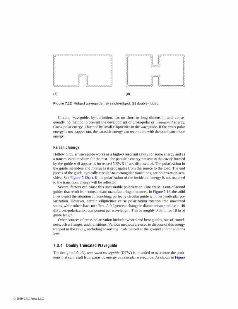
Circular waveguide, by definition, has no short or long dimension and, conse-quently, no method to prevent the development of cross-polar or orthogonal energy.Cross-polar energy is formed by small ellipticities in the waveguide. If the cross-polarenergy is not trapped out, the parasitic energy can recombine with the dominant-modeenergy.
Parasitic Energy
Hollow circular waveguide works as a high-Q resonant cavity for some energy and asa transmission medium for the rest. The parasitic energy present in the cavity formedby the guide will appear as increased VSWR if not disposed of. The polarization inthe guide meanders and rotates as it propagates from the source to the load. The endpieces of the guide, typically circular-to-rectangular transitions, are polarization-sen-sitive. See Figure 7.13(a). If the polarization of the incidental energy is not matchedto the transition, energy will be reflected.
Several factors can cause this undesirable polarization. One cause is out-of-roundguides that result from nonstandard manufacturing tolerances. In Figure 7.13, the solidlines depict the situation at launching: perfectly circular guide with perpendicular po-larization. However, certain ellipticities cause polarization rotation into unwantedstates, while others have no effect. A 0.2 percent change in diameter can produce a –40dB cross-polarization component per wavelength. This is roughly 0.03 in for 18 in ofguide length.
Other sources of cross polarization include twisted and bent guides, out-of-round-ness, offset flanges, and transitions. Various methods are used to dispose of this energytrapped in the cavity, including absorbing loads placed at the ground and/or antennalevel.
7.3.4 Doubly Truncated Waveguide
The design of doubly truncated waveguide (DTW) is intended to overcome the prob-lems that can result from parasitic energy in a circular waveguide. As shown in Figure
Figure 7.12 Ridged waveguide: (a) single-ridged, (b) double-ridged.
(a) (b)
© 1999 CRC Press LLC

7.14, DTW consists of an almost elliptical guide inside a circular shell. This guidedoes not support cross polarization; tuners and absorbing loads are not required. Thelow windload of hollow circular guide is maintained, except for the flange area.
Each length of waveguide is actually two separate pieces: a doubly truncated centersection and a circular outer skin, joined at the flanges on each end. A large hole in thebroadwall serves to pressurize the circular outer skin. Equal pressure inside the DTWand inside the circular skin ensures that the guide will not “breathe” or buckle as a resultof rapid temperature changes.
DTW exhibits about 3 percent higher windloading than an equivalent run of circularwaveguide (because of the transition section at the flange joints), and 32 percent lowerloading than comparable rectangular waveguide.
7.3.5 Impedance Matching
The efficient flow of power from one type of transmission medium to another requiresmatching of the field patterns across the boundary to launch the wave into the secondmedium with a minimum of reflections. Coaxial line typically is matched into rectan-gular waveguide by extending the center conductor of the coax through the broadwall
RF and Switching 377
Figure 7.13 The effects of parasitic energy in circular waveguide: (a) trappedcross-polarization energy, (b) delayed transmission of the trapped energy.
(a)
(b)
© 1999 CRC Press LLC

of the guide, parallel to the electric field lines across the guide. Alternatively, the cen-ter conductor can be formed into a loop and oriented to couple the magnetic field tothe guide mode.
Standing waves are generally to be avoided in waveguide for the same reasons thatthey are to be avoided in transmission lines. Accordingly, it is usually necessary to pro-vide impedance-matching systems in waveguides to eliminate standing waves. One ap-proach involves the introduction of a compensating reflection in the vicinity of a loadthat neutralizes the standing waves that would exist in the system because of an imper-fect match. A probe or tuning screw commonly is used to accomplish this, as illustratedin Figure 7.15. The tuning screw projects into the waveguide in a direction parallel tothe electric field. This is equivalent to shunting a capacitive load across the guide. Thesusceptance of the load increases with extension into the guide up to 1/4 wavelength.When the probe is exactly 1/4 wavelength long, it becomes resonant and causes theguide to behave as though there were an open circuit at the point of the resonant probe.Probes longer than 1/4 wavelength but shorter than 3/4 wavelength introduce inductiveloading. The extent to which such a probe projects into the waveguide determines thecompensating reflection, and the position of the probe with respect to the standing wavepattern to be eliminated determines the phasing of the reflected wave.
Dielectric slugs produce an effect similar to that of a probe. The magnitude of the ef-fect depends upon the following considerations:
• The dielectric constant of the slug
• Thickness of the slug in an axial direction
• Whether the slug extends entirely across the waveguide
The phase of the reflected wave is controlled by varying the axial position of the slug.
Figure 7.14 Physical construction of doubly truncated waveguide.
© 1999 CRC Press LLC

There are several alternatives to the probe and slug for introducing controllable ir-regularity for impedance matching, including a metallic barrier or window placed atright angles to the axis of the guide, as illustrated in Figure 7.16. Three configurationsare shown:
• The arrangement illustrated in Figure 7.16a produces an effect equivalent toshunting the waveguide with an inductive reactance.
• The arrangement shown in Figure 7.16b produces the effect of a shunt capacitivesusceptance.
• The arrangement shown in Figure 7.16c produces an inductive shuntsusceptance.
The waveguide equivalent of the coaxial cable tuning stub is a tee section, illustratedin Figure 7.17. The magnitude of the compensating effect is controlled by the positionof the short-circuiting plug in the branch. The phase of the compensating reflectedwave produced by the branch is determined by the position of the branch in the guide.
Waveguide Filters
A section of waveguide beyond cutoff constitutes a simple high-pass reflective filter.Loading elements in the form of posts or stubs may be employed to supply thereactances required for conventional lumped-constant filter designs.
Absorption filters prevent the reflection of unwanted energy by incorporating lossymaterial in secondary guides that are coupled through leaky walls (small sections of
Figure 7.15 A probe configured to introduce a reflection in a waveguide that is adjust-able in magnitude and phase.
© 1999 CRC Press LLC

guide beyond cutoff in the passband). Such filters typically are used to suppress har-monic energy.
7.3.6 Installation Considerations
Waveguide system installation is both easier and more difficult than traditional trans-mission line installation. There is no inner conductor to align, but alignment pinsmust be set and more bolts are required per flange. Transition hardware to accommo-date loads and coax-to-waveguide interfacing also is required.
Flange reflections can add up in phase at certain frequencies, resulting in highVSWR. The length of the guide must be chosen so that flange reflection buildup doesnot occur within the operating bandwidth.
Flexible sections of waveguide are used to join rigid sections or components thatcannot be aligned otherwise. Flexible sections also permit controlled physical move-ment resulting from thermal expansion of the line. Such hardware is available in a vari-ety of forms. Corrugated guide commonly is produced by shaping thin-wall seamlessrectangular tubing. Flexible waveguide can accommodate only a limited amount of me-chanical movement. Depending on the type of link, the manufacturer may specify amaximum number of bends.
Figure 7.16 Waveguide obstructions used to introduce compensating reflections: (a)inductive window, (b) capacitive window, (c) post (inductive) element.
(a) (b)
(c)
© 1999 CRC Press LLC

Tuning
Circular waveguide must be tuned. This requires a two-step procedure. First, thecross-polar TE1,1 component is reduced, primarily through axial ratio compensators ormode optimizers. These devices counteract the net system ellipticity and indirectlyminimize cross-polar energy. The cross-polar filters also may be rotated to achievemaximum isolation between the dominant and cross-polar modes. Cross-polar energymanifests itself as a net signal rotation at the end of the waveguide run. A perfect sys-tem would have a net rotation of zero.
In the second step, tuning slugs at both the top and bottom of the waveguide run areadjusted to reduce the overall system VSWR. Tuning waveguide can be a complicatedand time-consuming procedure. Once set, however, tuning normally does not drift andmust be repeated only if major component changes are made.
Waveguide Hardware
Increased use of waveguide has led to the development of waveguide-based hardwarefor all elements from the output of the RF generator to the load. Waveguide-based fil-ters, elbows, directional couplers, switches, combiners, and diplexers are currentlyavailable. The RF performance of a waveguide component is usually better than thesame item in coax. This is especially true in the case of diplexers and filters. Wave-guide-based hardware provides lower attenuation and greater power-handling capa-bility for a given physical size.
Figure 7.17 Waveguide stub elements used to introduce compensating reflections: (a)series tee element, (b) shunt tee element.
(a) (b)
© 1999 CRC Press LLC

7.3.7 Cavity Resonators
Any space completely enclosed by conducting walls can contain oscillating electro-magnetic fields. Such a cavity possesses certain frequencies at which it will resonatewhen excited by electrical oscillations. These cavity resonators find extensive use asresonant circuits at VHF and above. (The use of cavities in power grid tube amplifiersis discussed in Chapter 4.) Advantages of cavity resonators over conventional LC cir-cuits include:
• Simplicity in design.
• Relatively large physical size compared with alternative methods of obtainingresonance. This attribute is important in high-power, high-frequency applica-tions.
• High Q.
• The capability to configure the cavity to develop an extremely high shunt imped-ance.
Cavity resonators commonly are used at wavelengths on the order of 10 cm or less.The simplest cavity resonator is a section of waveguide shorted at each end with a
length l equal to:
lg=
λ2
(7.12)
Where:λ g = the guide wavelength
This configuration results in a resonance similar to that of a 1/2-wavelength transmis-sion line short-circuited at the receiving end.
A sphere or any other enclosed surface (irrespective of how irregular the outline)also may be used to form a cavity resonator.
Any given cavity is resonant at a number of frequencies, corresponding to the differ-ent possible field conditions that can exist within the space. The resonance having thelongest wavelength (lowest frequency) is termed the dominant or fundamental reso-nance. The resonant wavelength is proportional to the size of the resonator. If all di-mensions are doubled, the wavelength corresponding to resonance will likewise bedoubled. The resonant frequency of a cavity can be changed by incorporating one ormore of the following mechanisms:
• Altering the mechanical dimensions of the cavity. Small changes can be achievedby flexing walls, but large changes require some form of sliding member.
• Coupling reactance into the resonator through a coupling loop.
• Introducing a movable copper paddle into the cavity. A paddle placed inside theresonator will affect the normal distribution of flux and tend to raise the resonantfrequency by an amount determined by the orientation of the paddle.
© 1999 CRC Press LLC

The Q of a cavity resonator has the same significance as for a conventional resonantcircuit. Q can be defined for a cavity by the following relationship:
QE
Es
l
= 2π (7.13)
Where:Es = energy storedEl = energy lost per cycle
The energy stored is proportional to the square of the magnetic flux density integratedthroughout the volume of the resonator. The energy lost in the walls is proportional tothe square of the magnetic flux density integrated over the surface of the cavity. Toobtain high Q, the resonator should have a large ratio of volume to surface area, be-cause it is the volume that stores energy and the surface area that dissipates energy.
Coupling can be obtained from a resonator by means of a coupling loop or couplingelectrode. Magnetic coupling is accomplished through the use of a loop oriented so asto enclose magnetic flux lines existing in the desired mode of operation. This techniqueis illustrated in Figure 7.18. A current passed through the loop will excite oscillations ofthis mode. Conversely, oscillations existing in the resonator will induce a voltage in thecoupling loop. The magnitude of the coupling can be controlled by rotating the loop;the coupling reduces to zero when the plane of the loop is parallel to the magnetic flux.
Coupling of a resonator also may be accomplished through the use of a probe oropening in one wall of the cavity.
7.4 RF Combiner and Diplexer SystemsThe basic purpose of an RF combiner is to add two or more signals to produce an out-put signal that is a composite of the inputs. The combiner performs this signal addi-tion while providing isolation between inputs. Combiners perform other functions aswell, and can be found in a wide variety of RF equipment utilizing power vacuumtubes. Combiners are valuable devices because they permit multiple amplifiers to
Figure 7.18 Cavity resonator coupling: (a) coupling loop, (b) equivalent circuit.
(a) (b)
© 1999 CRC Press LLC

drive a single load. The isolation provided by the combiner permits tuning adjust-ments to be made on one amplifier—including turning it on or off—without signifi-cantly affecting the operation of the other amplifier. In a typical application, two am-plifiers drive the hybrid and provide two output signals:
• A combined output representing the sum of the two input signals, typically di-rected toward the antenna.
• A difference output representing the difference in amplitude and phase betweenthe two input signals. The difference output typically is directed toward a dummy(reject) load.
For systems in which more than two amplifiers must be combined, two or morecombiners are cascaded.
Diplexers are similar in nature to combiners but permit the summing of output sig-nals from two or more amplifiers operating at different frequencies. This allows, for ex-ample, the outputs of several transmitters operating on different frequencies to utilize asingle broadband antenna.
7.4.1 Passive Filters
A filter is a multiport-network designed specifically to respond differently to signalsof different frequency [1]. This definition excludes networks, which incidentally be-have as filters, sometimes to the detriment of their main purpose. Passive filters areconstructed exclusively with passive elements (i.e., resistors, inductors, and capaci-tors). Filters are generally categorized by the following general parameters:
• Type
• Alignment (or class)
• Order
Filter Type
Filters are categorized by type, according to the magnitude of the frequency response,as one of the following [1]:
• Low-pass (LP)
• High-pass (HP)
• Band-pass (BP)
• Band-stop (BS).
The terms band-reject or notch are also used as descriptive of the BS filter. The termall-pass is sometimes applied to a filter whose purpose is to alter the phase anglewithout affecting the magnitude of the frequency response. Ideal and practical inter-pretations of the types of filters and the associated terminology are illustrated in Fig-ure 7.19.
© 1999 CRC Press LLC

In general, the voltage gain of a filter in the stop band (or attenuation band) is lessthan 2 2 (≈ 0.707) times the maximum voltage gain in the pass band. In logarithmicterms, the gain in the stop band is at least 3.01 dB less than the maximum gain in thepass band. The cutoff (break or corner) frequency separates the pass band from the stopband. In BP and BS filters, there are two cutoff frequencies, sometimes referred to asthe lower and upper cutoff frequencies. Another expression for the cutoff frequency ishalf-power frequency, because the power delivered to a resistive load at cutoff fre-quency is one-half the maximum power delivered to the same load in the pass band. ForBP and BS filters, the center frequency is the frequency of maximum or minimum re-sponse magnitude, respectively, and bandwidth is the difference between the upper andlower cutoff frequencies. Rolloff is the transition from pass band to stop band and isspecified in gain unit per frequency unit (e.g., gain unit/Hz, dB/decade, dB/octave, etc.)
Filter Alignment
The alignment (or class) of a filter refers to the shape of the frequency response [1].Fundamentally, filter alignment is determined by the coefficients of the filter network
Figure 7.19 Filter characteristics by type: (a) low-pass, (b) high-pass, (c) bandpass, (d)bandstop. (From [1]. Used with permission.)
(a) (b)
(c) (d)
© 1999 CRC Press LLC

transfer function, so there are an indefinite number of filter alignments, some ofwhich may not be realizable. The more common alignments are:
• Butterworth
• Chebyshev
• Bessel
• Inverse Chebyshev
• Elliptic (or Cauer)
Each filter alignment has a frequency response with a characteristic shape, which pro-vides some particular advantage. (See Figure 7.20.) Filters with Butterworth,Chebyshev, or Bessel alignment are called all-pole filters because their low-passtransfer functions have no zeros. Table 7.3 summarizes the characteristics of the stan-dard filter alignments.
Filter Order
The order of a filter is equal to the number of poles in the filter network transfer func-tion [1]. For a lossless LC filter with resistive (nonreactive) termination, the numberof reactive elements (inductors or capacitors) required to realize a LP or HP filter isequal to the order of the filter. Twice the number of reactive elements are required torealize a BP or a BS filter of the same order. In general, the order of a filter deter-mines the slope of the rolloff—the higher the order, the steeper the rolloff. At fre-quencies greater than approximately one octave above cutoff (i.e., f > 2 fc), the rollofffor all-pole filters is 20n dB/decade (or approximately 6n dB/octave), where n is the
Figure 7.20 Filter characteristics by alignment, third-order, all-pole filters: (a) magni-tude, (b) magnitude in decibels. (From [1]. Used with permission.)
(a) (b)
© 1999 CRC Press LLC

order of the filter (Figure 7.21). In the vicinity of fc, both filter alignment and filter or-der determine rolloff.
7.4.2 Four-Port Hybrid Combiner
A hybrid combiner (coupler) is a reciprocal four-port device that can be used for ei-ther splitting or combining RF energy over a wide range of frequencies. An explodedview of a typical 3 dB 90° hybrid is illustrated in Figure 7.22. The device consists oftwo identical parallel transmission lines coupled over a distance of approximatelyone-quarter wavelength and enclosed within a single outer conductor. Ports at the
Table 7.3 Summary of Standard Filter Alignments (After [1].)
Alignment Pass BandDescription
Stop BandDescription
Comments
Butterworth Monotonic Monotonic All-pole; maximallyflat
Chebyshev Rippled Monotonic All-poleBessel Monotonic Monotonic All-pole; constant
phase shiftInverse Chebyshev Monotonic RippledElliptic (or Cauer) Rippled Rippled
Figure 7.21 The effects of filter order on rolloff (Butterworth alignment). (From [1]. Usedwith permission.)
© 1999 CRC Press LLC

same end of the coupler are in phase, and ports at the opposite end of the coupler arein quadrature (90° phase shift) with respect to each other.
The phase shift between the two inputs or outputs is always 90° and is virtually inde-pendent of frequency. If the coupler is being used to combine two signals into one out-put, these two signals must be fed to the hybrid in phase quadrature. When the coupler isused as a power splitter, the division is equal (half-power between the two ports). Thehybrid presents a constant impedance to match each source.
Operation of the combiner can best be understood through observation of the devicein a practical application. Figure 7.23 shows a four-port hybrid combiner used to addthe outputs of two transmitters to feed a single load. The combiner accepts one RFsource and splits it equally into two parts. One part arrives at output port C with 0°phase (no phase delay; it is the reference phase). The other part is delayed by 90° at portD. A second RF source connected to input port B, but with a phase delay of 90°, alsowill split in two, but the signal arriving at port C now will be in phase with source 1, andthe signal arriving at port D will cancel, as shown in the figure.
Output port C, the summing point of the hybrid, is connected to the load. Output portD is connected to a resistive load to absorb any residual power resulting from slight dif-ferences in amplitude and/or phase between the two input sources. If one of the RF in-puts fails, half of the remaining transmitter output will be absorbed by the resistive loadat port D.
The four-port hybrid works only when the two signals being mixed are identical infrequency and amplitude, and when their relative phase is 90°.
Operation of the hybrid can best be described by a scattering matrix in which vectorsare used to show how the device operates. Such a matrix is shown in Table 7.4. In a 3 dBhybrid, two signals are fed to the inputs. An input signal at port 1 with 0° phase will ar-rive in phase at port 3, and at port 4 with a 90° lag (–90°) referenced to port 1. If the sig-nal at port 2 already contains a 90° lag (–90° referenced to port 1), both input signalswill combine in phase at port 4. The signal from port 2 also experiences another 90°
Figure 7.22 Physical model of a 90° hybrid combiner.
© 1999 CRC Press LLC

change in the hybrid as it reaches port 3. Therefore, the signals from ports 1 and 2 can-cel each other at port 3.
If the signal arriving at port 2 leads by 90° (mode 1 in the table), the combined powerfrom ports 1 and 2 appears at port 4. If the two input signals are matched in phase (mode4), the output ports (3 and 4) contain one-half of the power from each of the inputs.
If one of the inputs is removed, which would occur in a transmitter failure, only onehybrid input receives power (mode 5). Each output port then would receive one-half theinput power of the remaining transmitter, as shown.
The input ports present a predictable load to each amplifier with a VSWR that islower than the VSWR at the output port of the combiner. This characteristic resultsfrom the action of the difference port, typically connected to a dummy load. Reflectedpower coming into the output port will be directed to the reject load, and only a portionwill be fed back to the amplifiers. Figure 7.24 illustrates the effect of output portVSWR on input port VSWR, and on the isolation between ports.
As noted previously, if the two inputs from the separate amplifiers are not equal inamplitude and not exactly in phase quadrature, some power will be dissipated in the dif-ference port reject load. Figure 7.25 plots the effect of power imbalance, and Figure7.26 plots the effects of phase imbalance. The power lost in the reject load can be re-duced to a negligible value by trimming the amplitude and/or phase of one (or both) am-plifiers.
7.4.3 Non-Constant-Impedance Diplexer
Diplexers are used to combine amplifiers operating on different frequencies (and atdifferent power levels) into a single output. Such systems typically are utilized to sumdifferent transmitter outputs to feed a single broadband antenna.
Figure 7.23 Operating principles of a hybrid combiner. This circuit is used to add twoidentical signals at inputs A and B.
© 1999 CRC Press LLC

Table 7.4 Single 90° Hybrid System Operating Modes
© 1999 CRC Press LLC

The branch diplexer is the typical configuration for a diplexer that does not exhibitconstant-impedance inputs. As shown in Figure 7.27, the branch diplexer consists oftwo banks of filters each feeding into a coaxial tee. The electrical length between eachfilter output and the centerline of the tee is frequency-sensitive, but this fact is more of atuning nuisance than a genuine user concern.
For this type of diplexer, all of the electrical parameters are a function of the filtercharacteristics. The VSWR, insertion loss, group delay, and rejection/isolation will bethe same for the overall system as they are for the individual banks of cavities. The ma-jor limitation of this type of combiner is the degree of isolation that can be obtained forclosely spaced channels.
7.4.4 Constant-Impedance Diplexer
The constant-impedance diplexer employs 3 dB hybrids and filters with a terminatingload on the isolated port. The filters in this type of combiner can be either notch-typeor bandpass-type. The performance characteristics are noticeably different for eachdesign.
Figure 7.24 The effects of load VSWR on input VSWR and isolation: (a) respectivecurves, (b) coupler schematic.
(a)
(b)
© 1999 CRC Press LLC

Figure 7.26 Phase sensitivity of a hybrid coupler.
Figure 7.25 The effects of power imbalance at the inputs of a hybrid coupler.
© 1999 CRC Press LLC

Band-Stop Diplexer
The band-stop (notch) constant-impedance diplexer is configured as shown in Figure7.28. For this design, the notch filters must have a high Q response to keep insertionloss low in the passband skirts. The high Q characteristic results in a sharp notch. De-pending on the bandwidth required of the diplexer, two or more cavities may be lo-cated in each leg of the diplexer. They are typically stagger tuned, one high and onelow for the two-cavity case. With this dual-cavity reject response in each leg of theband-stop diplexer system, the following analysis explains the key performance spec-ifications.
If frequency f1 is fed into the top left port of Figure 7.28, it will be split equally intothe upper and lower legs of the diplexer. Both of these signals will reach the filters intheir respective leg and be rejected/reflected back toward the input hybrid, recombine,and emerge through the lower left port, also known as the wideband output.
The VSWR looking into the f1 input is near 1:1 at all frequencies in the band. Withinthe bandwidth of the reject skirts, the observed VSWR is equal to the termination of thewideband output. Outside of the passband, the signals will pass by the cavities, enter therightmost hybrid, recombine, and emerge into the dummy load. Consequently, theout-of-band VSWR is, in fact, the VSWR of the load.
The insertion loss from the f1 input to the wideband output is low, typically on the or-der of 0.1 dB at carrier. This insertion loss depends on perfect reflection from the cavi-ties. As the rejection diminishes on the skirts of the filters, the insertion loss from f1 tothe wideband output increases.
The limitation in reject bandwidth of the cavities causes the insertion loss to rise atthe edges of the passband. The isolation from f1 to the wideband input consists of a com-bination of the reject value of the cavities plus the isolation of the rightmost hybrid.
Figure 7.27 Non-constant-impedance branch diplexer. In this configuration, two banksof filters feed into a coaxial tee.
© 1999 CRC Press LLC

A signal entering at f1 splits and proceeds in equal halves rightward through both theupper and lower legs of the diplexer. It is rejected by the filters at carrier and, to a lesserextent, on both sides of the carrier. Any residual signal that gets by the cavities reachesthe rightmost hybrid. There it recombines and emerges from the load port. The hybridprovides a specified isolation from the load port to the wideband input port. This hybridisolation must be added to the filter rejection to obtain the total isolation from the f1 in-put to the wideband input.
If a signal is fed into the wideband input of the combiner shown in Figure 7.28, theenergy will split equally and proceed leftward along the upper and lower legs of the di-plexer. Normally, f1 is not fed into the wideband input. If it were, f1 would be rejected bythe notch filters and recombine into the load. All other signals sufficiently removedfrom f1 will pass by the cavities with minimal insertion loss and recombine into thewideband output.
The VSWR looking into the wideband input is equal to the VSWR at the output forfrequencies other than f1. If f1 were fed into the wideband input, the VSWR would beequal to the VSWR of the load.
Isolation from the wideband input to the f1 input is simply the isolation available inthe leftmost 3 dB hybrid. This isolation is usually inadequate for high-power applica-tions. To increase the isolation from the wideband input to the f1 input, it is necessary touse additional cavities between the f1 transmitter and the f1 input that will reject the fre-quencies fed into the wideband input. Unfortunately, adding these cavities to the input
Figure 7.28 Band-stop (notch) constant-impedance diplexer module. This design in-corporates two 3 dB hybrids and filters, with a terminating load on the isolated port.
© 1999 CRC Press LLC

line also cancels the constant-impedance input. Although the notch diplexer as shownin the figure is truly a constant-impedance type of diplexer, the constant impedance ispresented to the two inputs by virtue of using the hybrids at the respective inputs.
The hybrids essentially cause the diplexer to act as an absorptive type of filter to allout-of-band signals. The out-of-band signals generated by the transmitter are absorbedby the load rather than reflected to the transmitter.
If a filter is added to the input to supplement isolation, the filter will reflect someout-of-band signals back at the transmitter. The transmitter then will be seeing thepassband impedance of this supplemental filter rather than the constant impedance ofthe notch diplexer. This is a serious deficiency for applications that require a true con-stant-impedance input.
Bandpass Constant-Impedance Diplexer
The bandpass constant-impedance diplexer is shown in Figure 7.29. This systemtakes all of the best features of diplexers and combines them into one unit. It also pro-vides a constant-impedance input that need not be supplemented with input cavitiesthat rob the diplexer of its constant-impedance input.
The bandpass filters exhibit good bandwidth, providing near 1:1 VSWR across theoperating bandpass. Insertion is low at carrier (0.28 dB is typical), rising slightly atbandpass extremes. Diplexer rejection, when supplemented by isolation of the hybrids,provides ample transmitter-to-transmitter isolation. Group delay is typically excep-tional, providing performance specifications similar to those of a branch-stylebandpass system. This configuration has the additional capability of providing highport-to-port isolation between closely spaced operating channels, as well as a true con-stant-impedance input.
Figure 7.29 Bandpass constant-impedance diplexer.
© 1999 CRC Press LLC

The hybrids shown in Figure 7.29 work in a manner identical to those described for aband-stop diplexer. However, the bandpass filters cause the system to exhibit perfor-mance specifications that exceed the band-stop system in every way. Consider a signalentering at the f1 input.
Within the passbands of the filters, which are tuned to f1, the VSWR will be near 1:1at carrier, rising slightly at the bandpass extremes. Because of the characteristic of theleftmost hybrid, the VSWR is, in fact, a measure of the similarity of response of the topand bottom bands of filters. The insertion loss looking from the f1 input to the widebandoutput will be similar to the insertion loss of the top and bottom filters individually. Avalue of approximately 0.28 dB at carrier is typical.
Both the insertion loss and group delay can be determined by the design bandwidthof the filters. Increasing bandwidth causes the insertion loss and group delay deviationto decrease. Unfortunately, as the bandwidth increases with a given number of cavities,the isolation suffers for closely spaced channels because the reject skirt of the filter de-creases with increasing bandwidth.
Isolation of f1 to the wideband input is determined as follows: A signal enters at the f1
input, splits equally into the upper and lower banks of filters, passes with minimal lossthrough the filters, and recombines into the wideband output of the rightmost hybrid.Both the load and the wideband input ports are isolated by their respective hybrids tosome given value below the f1 input level. Isolation of the f1 input to the wideband inputis supplemented by the reject skirt of the next module.
A signal fed into the wideband input could be any frequency removed from f1 bysome minimal amount. As the wideband signal enters, it will be split into equal halvesby the hybrid, then proceed to the left until the two components reach the reject skirts ofthe filters. The filters will shunt all frequencies removed from f1 by some minimalamount. If the shunt energy is in phase for the given frequency when the signal is re-flected back to the right hybrid, it will recombine into the wideband output. The VSWRunder these conditions will be equal to the termination at the wideband output. If the re-ject skirts of the filter are sufficient, the insertion loss from wideband input towideband output will be minimal (0.03 dB is typical).
The isolation from the wideband input to f1 can be determined as follows: A signalenters at the wideband input, splits equally into upper and lower filters, and is rejectedby the filters. Any residual signal that passes through the filters in spite of the rejectionstill will be in the proper phase to recombine into the load, producing additional isola-tion to the f1 input port. Thus, the isolation of the wideband input to the f1 input is thesum of the rejection from the filters and from the left hybrid.
Isolation of f1 to f2
Extending the use of the diplexer module into a multiplexer application supplementsthe deficient isolation described previously (narrowband input performance), whilemaintaining the constant-impedance input. In a multiplexer system, the wideband in-put of one module is connected to the wideband output of the next module, as illus-trated in Figure 7.30.
© 1999 CRC Press LLC

Figure 7.30 Schematic diagram of a six-module bandpass multiplexer. This configuration accommodates a split antenna designand incorporates patch panels for bypass purposes.
© 1999 C
RC
Press LL
C

It has already been stated that the isolation from the f1 input to the wideband input isdeficient, but additional isolation is provided by the isolation of the wideband output tothe f2 input of the next module. Consider that f1 has already experienced 30 dB isolationto the wideband input of the same module. When this signal continues to the next mod-ule through the wideband output of module 2, it will be split into equal halves and pro-ceed to the left of module 2 until it reaches the reject skirts of the filters in module 2. As-sume that these filters are tuned to f2 and reject f1 by at least 25 dB. The combined totalisolation of f1 to f2 is the sum of the 30 dB of the right hybrid in module 1, plus the 25 dBof the reject skirts of module 2, for a total of 55 dB.
Intermodulation Products
The isolation just described is equal in magnitude to that for a band-stop module, butit provides further protection against the generation of intermodulation products. Themost troublesome intermodulation (intermod) products usually occur when an incom-ing (secondary) signal mixes with the second harmonic of a primary transmitter. (Theproperties of intermodulation are discussed in more detail in Chapter 10.)
When the primary transmitter is operating on frequency A, the intermod will occurat the frequency( )2 × −A B. This formula invariably places the intermod from the pri-mary transmitter symmetrically about the operating frequency. By an interesting coin-cidence, the bandpass filters in the bandpass module also provide symmetrical rejectresponse on both sides of the primary operating frequency.
Assume again that the incoming signal is attenuated by 30 dB in the respective hy-brid and by 25 dB in the filter, for a total of 55 dB. If an intermod still is generated inspite of this isolation, it will emerge on the other skirt of the filter attenuated by 25 dB.In the bandpass system, the incoming signal is attenuated by 55 dB and the resultingoutgoing spur by 25 dB, for a total of 80 dB suppression.
Interestingly, the entire 80 dB of attenuation is supplied by the diplexer regardless ofthe turnaround loss of the transmitter. The tendency toward wideband final stage am-plifiers in transmitters requires constant-impedance inputs. The transmitters also re-quire increased isolation because they offer limited turnaround loss.
Group Delay
Group delay in the bandpass multiplexer module is equal to the sum of thenarrowband input group delay and the wideband input group delay of all modules be-tween the input and the load (antenna). (Group delay is discussed in detail in Chapter10.) The narrowband input group delay is a U-shaped response, with minimum at cen-ter and rising to a maximum on both sides at the frequency where the reject rises to 3dB. Group delay then decreases rapidly at first, then more slowly.
If the bandwidth of the pass band is made such that the group delay is ±25 ns over±150 kHz (in an example system operating near 100 MHz), the 3 dB points will be at±400 kHz and the out-of-band group delay will fall rapidly at ±800 kHz and possibly±1.0 MHz. If there are no frequencies 800 kHz or 1.0 MHz removed upstream in othermodules, this poses no problem.
© 1999 CRC Press LLC

If modules upstream are tuned to 800 kHz or 1.0 MHz on either side, then the groupdelay (when viewed at the upstream module) will consist of its own narrowband inputgroup delay plus the rapidly falling group delay of the wideband input of the closelyspaced downstream module. Under these circumstances, if good group delay is desired,it is possible to utilize a group delay compensation module.
A group delay compensation module consists of a hybrid and two cavities used asnotch cavities. It typically provides a group delay response that is inverted, comparedwith a narrowband input group delay. Because group delay is additive, the inverted re-sponse subtracts from the standard response, effectively reducing the group delay devi-ation.
It should be noted that the improvement in group delay is obtained at a cost of inser-tion loss. In large systems (8 to 10 modules), the insertion loss can be high because ofthe cumulative total of all wideband losses. Under these conditions, it may be more pru-dent to accept higher group delay and retain minimal insertion loss.
7.4.5 Microwave Combiners
Hybrid combiners typically are used in microwave amplifiers to add the output energyof individual power modules to provide the necessary output from an RF generator.Quadrature hybrids effect a VSWR-canceling phenomenon that results inwell-matched power amplifier inputs and outputs that can be broadbanded withproper selection of hybrid tees. Several hybrid configurations are possible, includingthe following:
• Split-tee
• Branch-line
• Magic-tee
• Backward-wave
Key design parameters include coupling bandwidth, isolation, and ease of fabrication.The equal-amplitude quadrature-phase reverse-coupled TEM 1/4-wave hybrid is par-ticularly attractive because of its bandwidth and amenability to various physical im-plementations. Such a device is illustrated in Figure 7.31.
7.4.6 Hot Switching Combiners
Switching RF is nothing new. Typically, the process involves coaxial switches, cou-pled with the necessary logic to ensure that the “switch” takes place with no RF en-ergy on the contacts. This process usually takes the system off-line for a few secondswhile the switch is completed. Through the use of hybrid combiners, however, it ispossible to redirect RF signals without turning the carrier off. This process is referredto as hot switching. Figure 7.32 illustrates two of the most common switching func-tions (SPST and DPDT) available from hot switchers.
© 1999 CRC Press LLC

The unique phase-related properties of an RF hybrid make it possible to use the de-vice as a switch. The input signals to the hybrid in Figure 7.33a are equally powered butdiffer in phase by 90°. This phase difference results in the combined signals beingrouted to the output terminal at port 4. If the relative phase between the two input sig-nals is changed by 180°, the summed output then appears on port 3, as shown in Figure7.33b. The 3 dB hybrid combiner, thus, functions as a switch.
This configuration permits the switching of two RF generators to either of twoloads. Remember, however, that the switch takes place when the phase difference be-tween the two inputs is 90°. To perform the switch in a useful way requires adding ahigh-power phase shifter to one input leg of the hybrid. The addition of the phase shifterpermits the full power to be combined and switched to either output. This configurationof hybrid and phase shifter, however, will not permit switching a main or standby gener-ator to a main or auxiliary load (DPDT function). To accomplish this additional switch,a second hybrid and phase shifter must be added, as shown in Figure 7.34. This configu-ration then can perform the following switching functions:
• RF source 1 routed to output B
• RF source 2 routed to output A
• RF source 1 routed to output A
• RF source 2 routed to output B
The key element in developing such a switch is a high-power phase shifter that doesnot exhibit reflection characteristics. In this application, the phase shifter allows theline between the hybrids to be electrically lengthened or shortened. The ability to adjustthe relative phase between the two input signals to the second hybrid provides theneeded control to switch the input signal between the two output ports.
If a continuous analog phase shifter is used, the transfer switch shown in Figure 7.34also can act as a hot switchless combiner where RF generators 1 and 2 can be combined
Figure 7.31 Reverse-coupled 1/4-wave hybrid combiner.
© 1999 CRC Press LLC

and fed to either output A or B. The switching or combining functions are accomplishedby changing the physical position of the phase shifter.
Note that it does not matter whether the phase shifter is in one or both legs of the sys-tem. It is the phase difference (θ θ1 2− ) between the two input legs of the second hybridthat is important. With 2-phase shifters, dual drives are required. However, the phaseshifter needs only two positions. In a 1-phase shifter design, only a single drive is re-quired, but the phase shifter must have four fixed operating positions.
Figure 7.33 Hybrid switching configurations: (a) phase set so that the combined energyis delivered to port 4, (b) phase set so that the combined energy is delivered to port 3.
(a) (b)
Figure 7.32 Common RF switching configurations.
© 1999 CRC Press LLC

Phase Relationships
To better understand the dual-hybrid switching and combining process, it is necessaryto examine the primary switching combinations. Table 7.5 lists the various combina-tions of inputs, relative phase, and output configurations that are possible with thesingle-phase shifter design.
Using vector analysis, note that when two input signals arrive in phase (mode 1) atports 1 and 2 with the phase shifter set to 0°, the circuit acts like a crossover networkwith the power from input port 1 routed to output port 4. Power from input port 2 isrouted to output port 3. If the phase shifter is set to 180°, the routing changes, with port1 being routed to port 3 and port 2 being routed to port 4.
Mode 2 represents the case where one of the dual-input RF generators has failed.The output signal from the first hybrid arrives at the input to the second hybrid with a90° phase difference. Because the second hybrid introduces a 90° phase shift, the vec-tors add at port 4 and cancel at port 3. This effectively switches the working transmitterconnected to port 1 to output port 4, the load.
By introducing a 180° phase shift between the hybrids, as shown in modes 4 and 5, itis possible to reverse the circuit. This allows the outputs to be on the same side of the cir-cuit as the inputs. This configuration might be useful if generator 1 fails, and all powerfrom generator 2 is directed to a diplexer connected to output 4.
Normal operating configurations are shown in modes 6 and 7. When both genera-tors are running, it is possible to have the combined power routed to either output port.The switching is accomplished by introducing a ±90º phase shift between the hybrids.
As shown in the table, it is possible to operate in all the listed modes through the useof a single-phase shifter. The phase shifter must provide four different phase positions.A similar analysis would show that a 2-phase shifter design, with two positions for eachshifter, is capable of providing the same operational modes.
Figure 7.34 Additional switching and combining functions enabled by adding a secondhybrid and another phase shifter to a hot switching combiner.
© 1999 CRC Press LLC

Table 7.5 Operating Modes of the Dual 90° Hybrid/Single-Phase Shifter Combiner Sys-tem
© 1999 CRC Press LLC
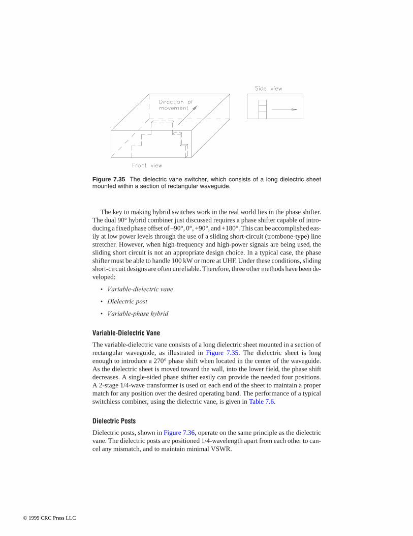
The key to making hybrid switches work in the real world lies in the phase shifter.The dual 90° hybrid combiner just discussed requires a phase shifter capable of intro-ducing a fixed phase offset of –90°, 0°, +90°, and +180°. This can be accomplished eas-ily at low power levels through the use of a sliding short-circuit (trombone-type) linestretcher. However, when high-frequency and high-power signals are being used, thesliding short circuit is not an appropriate design choice. In a typical case, the phaseshifter must be able to handle 100 kW or more at UHF. Under these conditions, slidingshort-circuit designs are often unreliable. Therefore, three other methods have been de-veloped:
• Variable-dielectric vane
• Dielectric post
• Variable-phase hybrid
Variable-Dielectric Vane
The variable-dielectric vane consists of a long dielectric sheet mounted in a section ofrectangular waveguide, as illustrated in Figure 7.35. The dielectric sheet is longenough to introduce a 270° phase shift when located in the center of the waveguide.As the dielectric sheet is moved toward the wall, into the lower field, the phase shiftdecreases. A single-sided phase shifter easily can provide the needed four positions.A 2-stage 1/4-wave transformer is used on each end of the sheet to maintain a propermatch for any position over the desired operating band. The performance of a typicalswitchless combiner, using the dielectric vane, is given in Table 7.6.
Dielectric Posts
Dielectric posts, shown in Figure 7.36, operate on the same principle as the dielectricvane. The dielectric posts are positioned 1/4-wavelength apart from each other to can-cel any mismatch, and to maintain minimal VSWR.
Figure 7.35 The dielectric vane switcher, which consists of a long dielectric sheetmounted within a section of rectangular waveguide.
© 1999 CRC Press LLC

Variable-Phase Hybrid
The variable-phase hybrid, shown in Figure 7.37, relies on a 90° hybrid, similar tothose used in a combiner. With a unit vector incident on port 1, the power is split bythe 90° hybrid. The signal at ports 3 and 4 is reflected by the short circuit. These re-flected signals are out of phase at port 1 and in phase at port 2. The relative phase ofthe hybrid can be changed by moving the short circuit.
The variable-phase hybrid is linear with respect to position. Noncontactingchoke-type short-circuits, with high front-to-back ratios, are typically used in the de-vice. The performance available from a typical high-power variable-phase switchlesscombiner is given in Table 7.7.
Type Input PhaseChange
(deg)
VSWR InputAttenuation
OutputAttenuation
1 (dB) 2 (dB) 3 (dB) 4 (dB)Singleinput
T1 180 1.06 - 39 0.1 39T1 0 1.05 - 39 39 0.1T2 180 1.05 39 - 39 0.1T2 0 1.06 39 - 0.1 39
Dual in-put
T1+T2 270 1.06 - - 0.1 36T1+T2 90 1.06 - - 36 0.1
Table 7.6 Typical Performance of a Dielectric Vane Phase Shifter
Figure 7.36 Dielectric post waveguide phase shifter.
© 1999 CRC Press LLC

7.4.7 Phased-Array Antenna Systems
The phased-array antenna, commonly used in radar applications, is a variation on thehot switching combiner systems discussed in the previous section. The hot switchingcombiner is used to control the flow of RF energy from one or more generators to twoor more loads, while the phased-array antenna is used to modify—in a controlledfashion—the radiating characteristics of an antenna.
Phased-array antennas are steered by tilting the phase front independently in two or-thogonal directions called the array coordinates. Scanning in either array coordinatecauses the beam to move along a cone whose center is at the center of the array. As thebeam is steered away from the array normal, the projected aperture in the beam’s direc-tion varies, causing the beamwidth to vary proportionately.
Arrays can be classified as either active or passive. Active arrays contain duplexersand amplifiers behind every element or group of elements of the array. Passive arraysare driven from a single feed point. Active arrays are capable of high-power operation.Both passive and active arrays must divide the signal from a single transmission lineamong all the elements of the system. This can be accomplished through one of the fol-lowing methods:
• Optical feed: a single feed, usually a monopulse horn, is used to illuminate the ar-ray with a spherical phase front, illustrated in Figure 7.38. Power collected by therear elements of the array is transmitted through the phase shifters to produce aplanar front and steer the array. The energy then may be radiated from the other
Figure 7.37 Variable-phase hybrid phase shifter.
© 1999 CRC Press LLC

side of the array or reflected and reradiated through the collecting elements. In thelatter case, the array acts as a steerable reflector.
• Corporate feed: a system utilizing a series-feed network (Figure 7.39) or paral-lel-feed network (Figure 7.40). Both designs use transmission-line componentsto divide the signal among the elements. Phase shifters can be located at the ele-ments or within the dividing network. Both the series- and parallel-feed systemshave several variations, as shown in the figures.
• Multiple-beam network: a system capable of forming simultaneous beams with agiven array. The Butler matrix, shown in Figure 7.41, is one such technique. Itconnects the N elements of a linear array to N feed points corresponding to Nbeam outputs. The phase shifter is one of the most critical components of the sys-tem. It produces controllable phase shift over the operating band of the array.Digital and analog phase shifters have been developed using both ferrites and pindiodes.
Frequency scan is another type of multiple-beam network, but one that does not re-quire phase shifters, dividers, or beam-steering computers. Element signals are cou-pled from points along a transmission line. The electrical path length between ele-ments is longer than the physical separation, so a small frequency change will cause aphase change between elements that is large enough to steer the beam. This techniquecan be applied only to one array coordinate. If a two-dimensional array is required,phase shifters normally are used to scan the other coordinate.
Phase-Shift Devices
The design of a phase shifter must meet two primary criteria:
• Low transmission loss
• High power-handling capability
Table 7.7 Typical Performance of a Variable-Phase Hybrid Phase Shifter
Type Input Phase Change(deg)
VSWR InputAttenuation
OutputAttenuation
1 (dB) 2 (dB) 3 (dB) 4 (dB)Singleinput
T1 180 1.06 - 36 0.1 52T1 0 1.04 - 36 50 0.1T2 180 1.06 36 - 52 0.1T2 0 1.07 36 - 0.1 50
Dualinput
T1+T2 270 1.06 - - 0.1 36T1+T2 90 1.06 - - 36 0.1
© 1999 CRC Press LLC

The Reggia-Spencer phase shifter meets both requirements. The device, illustrated inFigure 7.42, consists of a ferrite rod mounted inside a waveguide that delays the RFsignal passing through the waveguide, permitting the array to be steered. The amountof phase shift can be controlled by the current in the solenoid, because of the effect a
Figure 7.38 Optical antenna feed systems: (a) lens, (b) reflector.
(b)
(a)
© 1999 CRC Press LLC

magnetic field has on the permeability of the ferrite. This design is a reciprocal phaseshifter, meaning that the device exhibits the same phase shift for signals passing in ei-ther direction (forward or reverse). Nonreciprocal phase shifters also are available,where phase-shift polarity reverses with the direction of propagation.
Phase shifters also may be developed using pin diodes in transmission line net-works. One configuration, shown in Figure 7.43, uses diodes as switches to change thesignal path length of the network. A second type uses pin diodes as switches to connectreactive loads across a transmission line. When equal loads are connected with1/4-wave separation, a pure phase shift results.
Figure 7.39 Series-feed networks: (a) end feed, (b) center feed, (c) separate optimiza-tion, (d) equal path length, (e) series phase shifters.
(a) (b)
(c) (d)
(e)
© 1999 CRC Press LLC

Figure 7.40 Types of parallel-feed networks: (a) matched corporate feed, (b) reactivecorporate feed, (c) reactive stripline, (d) multiple reactive divider.
(a) (b)
(c) (d)
Figure 7.41 The Butler beam-forming network.
© 1999 CRC Press LLC

Radar System Duplexer
The duplexer is an essential component of any radar system. The switching elementsused in a duplexer include gas tubes, ferrite circulators, and pin diodes. Gas tubes arethe simplest. A typical gas-filled TR tube is shown in Figure 7.44. Low-power RF sig-nals pass through the tube with little attenuation. Higher-power signals, however,cause the gas to ionize and present a short circuit to the RF energy.
Figure 7.45 illustrates a balanced duplexer using hybrid junctions and TR tubes.When the transmitter is on, the TR tubes fire and reflect the RF power to the antennaport of the input hybrid. During the receive portion of the radar function, signals pickedup by the antenna are passed through the TR tubes and on to the receiver port of the out-put hybrid.
Newer radar systems often use a ferrite circulator as the duplexer. A TR tube is re-quired in the receiver line to protect input circuits from transmitter power reflected bythe antenna because of an imperfect match. A four-port circulator generally is usedwith a load between the transmitter and receiver ports so that power reflected by the TRtube is properly terminated.
Pin diode switches also have been used in duplexers to perform the protectiveswitching function of TR tubes. Pin diodes are more easily applied in coaxial circuitry,
Figure 7.42 Basic concept of a Reggia-Spencer phase shifter.
© 1999 CRC Press LLC

and at lower microwave frequencies. Multiple diodes are used when a single diode can-not withstand the expected power.
Microwave filters sometimes are used in the transmit path of a radar system to sup-press spurious radiation, or in the receive signal path to suppress spurious interference.
Figure 7.44 Typical construction of a TR tube.
Figure 7.43 Switched-line phase shifter using pin diodes.
© 1999 CRC Press LLC

Harmonic filters commonly are used in the transmission chain to absorb harmonicenergy output by the system, preventing it from being radiated or reflected back fromthe antenna. Figure 7.46 shows a filter in which harmonic energy is coupled outthrough holes in the walls of the waveguide to matched loads.
Narrowband filters in the receive path, often called preselectors, are built using me-chanically tuned cavity resonators or electrically tuned TIG resonators. Preselectorscan provide up to 80 dB suppression of signals from other radar transmitters in the sameRF band, but at a different operating frequency.
7.5 High-Power IsolatorsThe high-power ferrite isolator offers the ability to stabilize impedance, isolate the RFgenerator from load discontinuities, eliminate reflections from the load, and absorbharmonic and intermodulation products. The isolator also can be used to switch be-tween an antenna or load under full power, or to combine two or more generators intoa common load.
Isolators commonly are used in microwave transmitters at low power to protect theoutput stage from reflections. Until recently, however, the insertion loss of the ferritemade use of isolators impractical at high-power levels (25 kW and above). Ferrite isola-
Figure 7.45 Balanced duplexer circuit using dual TR tubes and two short-slot hybridjunctions: (a) transmit mode, (b) receive mode.
(a)
(b)
© 1999 CRC Press LLC

tors are now available that can handle 500 kW or more of forward power with less than0.1 dB of forward power loss.
7.5.1 Theory of Operation
High-power isolators are three-port versions of a family of devices known ascirculators. The circulator derives its name from the fact that a signal applied to oneof the input ports can travel in only one direction, as shown in Figure 7.47. The inputport is isolated from the output port. A signal entering port 1 appears only at port 2; itdoes not appear at port 3 unless reflected from port 2. An important benefit of thisone-way power transfer is that the input VSWR at port 1 is dependent only on theVSWR of the load placed at port 3. In most applications, this load is a resistive(dummy) load that presents a perfect load to the RF generator.
The unidirectional property of the isolator results from magnetization of a ferrite al-loy inside the device. Through correct polarization of the magnetic field of the ferrite,RF energy will travel through the element in only one direction (port 1 to 2, port 2 to 3,and port 3 to 1). Reversing the polarity of the magnetic field makes it possible for RFflow in the opposite direction. Recent developments in ferrite technology have resultedin high isolation with low insertion loss.
In the basic design, the ferrite is placed in the center of a Y-junction of three trans-mission lines, either waveguide or coax. Sections of the material are bonded together toform a thin cylinder perpendicular to the electric field. Even though the insertion loss islow, the resulting power dissipated in the cylinder can be as high as 2 percent of the for-
Figure 7.46 Construction of a dissipative waveguide filter.
© 1999 CRC Press LLC

ward power. Special provisions must be made for heat removal. It is efficient heat-re-moval capability that makes high-power operation possible.
The insertion loss of the ferrite must be kept low so that minimal heat is dissipated.Values of ferrite loss on the order of 0.05 dB have been produced. This equates to an ef-ficiency of 98.9 percent. Additional losses from the transmission line and matchingstructure contribute slightly to loss. The overall loss is typically less than 0.1 dB, or 98
Figure 7.47 Basic characteristics of a circulator: (a) operational schematic, (b) distrib-uted constant circulator, (c) lump constant circulator. (From [2]. Used with permission.)
(a)
(b)
(c)
© 1999 CRC Press LLC

percent efficiency. The ferrite element in a high-power system is usually water-cooledin a closed-loop path that uses an external radiator.
The two basic circulator implementations are shown in Figures 7.47a and 7.47b.These designs consist of Y-shaped conductors sandwiched between magnetized ferritediscs [2]. The final shape, dimensions, and type of material varies according to fre-quency of operation, power handling requirements, and the method of coupling. Thedistributed constant circulator is the older design; it is a broad-band device, not quite asefficient in terms of insertion loss and leg-to-leg isolation, and considerably more ex-pensive to produce. It is useful, however, in applications where broad-band isolation isrequired. More commonly today is the lump constant circulator, a less expensive andmore efficient, but narrow-band, design.
At least one filter is always installed directly after an isolator, because the ferrite ma-terial of the isolator generates harmonic signals. If an ordinary band-pass or band-re-ject filter is not to be used, a harmonic filter will be needed.
7.5.2 Applications
The high-power isolator permits an RF generator to operate with high performanceand reliability despite a load that is less than optimum. The problems presented by iceformations on a transmitting antenna provide a convenient example. Ice buildup willdetune an antenna, resulting in reflections back to the transmitter and high VSWR. Ifthe VSWR is severe enough, transmitter power will have to be reduced to keep thesystem on the air. An isolator, however, permits continued operation with no degrada-tion in signal quality. Power output is affected only to the extent of the reflected en-ergy, which is dissipated in the resistive load.
A high-power isolator also can be used to provide a stable impedance for devices thatare sensitive to load variations, such as klystrons. This allows the device to be tuned foroptimum performance regardless of the stability of the RF components located after theisolator. Figure 7.48 shows the output of a wideband (6 MHz) klystron operating into aresistive load, and into an antenna system. The power loss is the result of an impedancedifference. The periodicity of the ripple shown in the trace is a function of the distanceof the reflections from the source.
Hot Switch
The circulator can be made to perform a switching function if a short circuit is placedat the output port. Under this condition, all input power will be reflected back into thethird port. The use of a high-power stub on port 2, therefore, permits redirecting theoutput of an RF generator to port 3.
At odd 1/4-wave positions, the stub appears as a high impedance and has no effect onthe output port. At even 1/4-wave positions, the stub appears as a short circuit.Switching between the antenna and a test load, for example, can be accomplished bymoving the shorting element 1/4 wavelength.
© 1999 CRC Press LLC

Diplexer
An isolator may be configured to combine the aural and visual outputs of a TV trans-mitter into a single output for the antenna. The approach is shown in Figure 7.49 . Asingle notch cavity at the aural frequency is placed on the visual transmitter output
Figure 7.48 Output of a klystron operating into different loads through a high-power iso-lator: (a) resistive load, (b) an antenna system.
(a)
(b)
© 1999 CRC Press LLC

(circulator input), and the aural signal is added (as shown). The aural signal will berouted to the antenna in the same manner as it is reflected (because of the hybrid ac-tion) in a conventional diplexer.
Multiplexer
A multiplexer can be formed by cascading multiple circulators, as illustrated in Fig-ure 7.50. Filters must be added, as shown. The primary drawback of this approach isthe increased power dissipation that occurs in circulators nearest the antenna.
Figure 7.49 Use of a circulator as a diplexer in TV applications.
Figure 7.50 Using multiple circulators to form a multiplexer.
© 1999 CRC Press LLC

7.6 References1. Harrison, Cecil, “Passive Filters,” in The Electronics Handbook, Jerry C. Whitaker
(ed.), CRC Press, Boca Raton, Fla., pp. 279–290, 1996.2. Surette, Robert A., “Combiners and Combining Networks,” in The Electronics
Handbook, Jerry C. Whitaker (ed.), CRC Press, Boca Raton, Fla., pp. 1368–1381,1996.
7.7 BibliographyAndrew Corporation, “Broadcast Transmission Line Systems,” Technical Bulletin
1063H, Orland Park, IL, 1982.Andrew Corporation, “Circular Waveguide: System Planning, Installation and
Tuning,” Technical Bulletin 1061H, Orland Park, IL, 1980.Ben-Dov, O., and C. Plummer, “Doubly Truncated Waveguide,” Broadcast Engi-
neering, Intertec Publishing, Overland Park, KS, January 1989.Benson, K. B., and J. C. Whitaker, Television and Audio Handbook for Technicians
and Engineers, McGraw-Hill, New York, 1989.Cablewave Systems, “The Broadcaster’s Guide to Transmission Line Systems,” Tech-
nical Bulletin 21A, North Haven, CT, 1976.Cablewave Systems, “Rigid Coaxial Transmission Lines,” Cablewave Systems Cata-
log 700, North Haven, CT, 1989.Crutchfield, E. B. (ed.), NAB Engineering Handbook, 8th Ed., National Association of
Broadcasters, Washington, DC, 1992.DeComier, Bill, “Inside FM Multiplexer Systems,” Broadcast Engineering, Intertec
Publishing, Overland Park, KS, May 1988.Fink, D., and D. Christiansen (eds.), Electronics Engineers’ Handbook, 3rd Ed.,
McGraw-Hill, New York, 1989.Fink, D., and D. Christiansen (eds.), Electronics Engineers’ Handbook, 2nd Ed.,
McGraw-Hill, New York, 1982.Heymans, Dennis, “Hot Switches and Combiners,” Broadcast Engineering, Overland
Park, KS, December 1987.Jordan, Edward C., Reference Data for Engineers: Radio, Electronics, Computer and
Communications, 7th Ed., Howard W. Sams, Indianapolis, IN, 1985.Krohe, Gary L., “Using Circular Waveguide,” Broadcast Engineering, Intertec Pub-
lishing, Overland Park, KS, May 1986.Perelman, R., and T. Sullivan, “Selecting Flexible Coaxial Cable,” Broadcast Engi-
neering, Intertec Publishing, Overland Park, KS, May 1988.Stenberg, James T., “Using Super Power Isolators in the Broadcast Plant,” Proceed-
ings of the Broadcast Engineering Conference, Society of Broadcast Engineers, In-dianapolis, IN, 1988.
Terman, F. E., Radio Engineering, 3rd Ed., McGraw-Hill, New York, 1947.Vaughan, T., and E. Pivit, “High Power Isolator for UHF Television,” Proceedings of
the NAB Engineering Conference, National Association of Broadcasters, Washing-ton, DC, 1989.
Whitaker, Jerry C., G. DeSantis, and C. Paulson, Interconnecting Electronic Systems,CRC Press, Boca Raton, FL, 1993.
© 1999 CRC Press LLC

Whitaker, Jerry C., Radio Frequency Transmission Systems: Design and Operation,McGraw-Hill, New York, 1990.
© 1999 CRC Press LLC

Whitaker, Jerry C. “Chapter 8 – Cooling Considerations” Power Vacuum Tubes Handbook 2nd Edition.Ed. Jerry C. WhitakerBoca Raton: CRC Press LLC, 2000
© 1999 CRC Press LLC

Chapter
8Cooling Considerations
8.1 IntroductionAdequate cooling of the tube envelope and seals is one of the principal factors affect-ing vacuum tube life [1]. Deteriorating effects increase directly with the temperatureof the tube envelope and ceramic/metal seals. Inadequate cooling is almost certain toinvite premature failure of the device.
Tubes operated at VHF and above are inherently subjected to greater heating actionthan tubes operated at lower frequencies. This results directly from the following:
• The flow of larger RF charging currents into the tube capacitances at higher fre-quencies
• Increased dielectric losses at higher frequencies
• The tendency of electrons to bombard parts of the tube structure other than thenormal elements as the operating frequency is increased
Greater cooling, therefore, is required at higher frequencies. The technical data sheetfor a given tube type specifies the maximum allowable operating temperature. Forforced-air- and water-cooled tubes, the recommended amount of air or water is alsospecified in the data sheet. Both the temperature and quantity of coolant should bemeasured to be certain that cooling is adequate.
8.1.1 Thermal Properties
In the commonly used model for materials, heat is a form of energy associated withthe position and motion of the molecules, atoms, and ions of the material [2]. The po-sition is analogous with the state of the material and is potential energy, while the mo-tion of the molecules, atoms and ions is kinetic energy. Heat added to a materialmakes it hotter, and heat withdrawn from a material makes it cooler. Heat energy ismeasured in calories (cal), British Thermal Units (Btu), or joules. A calorie is theamount of energy required to raise the temperature of one gram of water one degreeCelsius (14.5 to 15.5 ºC). A Btu is the unit of energy necessary to raise the tempera-ture of one pound of water by one degree Fahrenheit. A joule is an equivalent amount
© 1999 CRC Press LLC
of energy equal to the work done when a force of one newton acts through a distanceof one meter.
Temperature is a measure of the average kinetic energy of a substance. It can also beconsidered a relative measure of the difference of the heat content between bodies.
Heat capacity is defined as the amount of heat energy required to raise the tempera-ture of one mole or atom of a material by one ºC without changing the state of the mate-rial. Thus, it is the ratio of the change in heat energy of a unit mass of a substance to itschange in temperature. The heat capacity, often referred to as thermal capacity, is acharacteristic of a material and is measured in cal/gram per ºC or Btu/lb per ºF.
Specific heat is the ratio of the heat capacity of a material to the heat capacity of areference material, usually water. Because the heat capacity of water is one Btu/lb andone cal/gram, the specific heat is numerically equal to the heat capacity.
Heat transfers through a material by conduction resulting when the energy of atomicand molecular vibrations is passed to atoms and molecules with lower energy. As heat isadded to a substance, the kinetic energy of the lattice atoms and molecules increases.This, in turn, causes an expansion of the material that is proportional to the temperaturechange, over normal temperature ranges. If a material is restrained from expanding orcontracting during heating and cooling, internal stress is established in the material.
8.1.2 Heal Transfer Mechanisms
The process of heat transfer from one point or medium to another is a result of tem-perature differences between the two. Thermal energy may be transferred by any ofthree basic modes:
• Conduction
• Convection
• Radiation
A related mode is the convection process associated with the change of phase of afluid, such as condensation or boiling. A vacuum tube amplifier or oscillator may useseveral of these mechanisms to maintain the operating temperature of the devicewithin specified limits.
Conduction
Heat transfer by conduction in solid materials occurs whenever a hotter region withmore rapidly vibrating molecules transfers a portion of its energy to a cooler regionwith less rapidly vibrating molecules. Conductive heat transfer is the most commonform of thermal exchange in electronic equipment. Thermal conductivity for solidmaterials used in electronic equipment spans a wide range of values, from excellent(high conductivity) to poor (low conductivity). Generally speaking, metals are thebest conductors of heat, whereas insulators are the poorest. Table 8.1 lists the thermalconductivity of materials commonly used in the construction (and environment) of
© 1999 CRC Press LLC

power vacuum tubes. Table 8.2 compares the thermal conductivity of various sub-stances as a percentage of the thermal conductivity of copper.
With regard to vacuum tube devices, conduction is just one of the cooling mecha-nisms involved in maintaining element temperatures within specified limits. At highpower levels, there is always a secondary mechanism that works to cool the device. Forexample, heat generated within the tube elements is carried to the cooling surfaces ofthe device by conduction. Convection or radiation then is used to remove heat from thetube itself.
Thermal conduction has been used successfully to cool vacuum tubes through directconnection of the anode to an external heat sink, but only at low power levels [1].
Table 8.2 Relative Thermal Conductivity of Various Materials As a Percentage of theThermal Conductivity of Copper
Material Relative ConductivitySilver 105Copper 100Berlox high-purity BeO 62Aluminum 55Beryllium 39Molybdenum 39Steel 9.1High-purity alumina 7.7Steatite 0.9Mica 0.18Phenolics, epoxies 0.13Fluorocarbons 0.05
Material Btu/(h·ft·°F W/(m·°CSilver 242 419Copper 228 395Gold 172 298Beryllia 140 242Phosphor bronze 30 52Glass (borosilicate) 0.67 1.67Mylar 0.11 0.19Air 0.015 0.026
Table 8.1 Thermal Conductivity of Common Materials
© 1999 CRC Press LLC

Convection
Heat transfer by natural convection occurs as a result of a change in the density of afluid (including air), which causes fluid motion. Convective heat transfer between aheated surface and the surrounding fluid is always accompanied by a mixing of fluidadjacent to the surface. Power vacuum tube devices relying on convective cooling in-variably utilize forced air or water passing through a heat-transfer element, typicallythe anode in a grid tube or the collector in a microwave tube [1]. This forced convec-tion provides for a convenient and relatively simple cooling system. In such an ar-rangement, the temperature gradient is confined to a thin layer of fluid adjacent to thesurface so that the heat flows through a relatively thin boundary layer. In the mainstream outside this layer, isothermal conditions exist.
Radiation
Cooling by radiation is a function of the transfer of energy by electromagnetic wavepropagation. The wavelengths between 0.1 and 100 m are referred to as thermal radi-ation wavelengths. The ability of a body to radiate thermal energy at any particularwavelength is a function of the body temperature and the characteristics of the surfaceof the radiating material. Figure 8.1 charts the ability to radiate energy for an ideal ra-diator, a blackbody, which, by definition, radiates the maximum amount of energy atany wavelength. Materials that act as perfect radiators are rare. Most materials radiateenergy at a fraction of the maximum possible value. The ratio of the energy radiatedby a given material to that emitted by a blackbody at the same temperature is termedemissivity. Table 8.3 lists the emissivity of various common materials.
8.1.3 The Physics of Boiling Water
The Nukiyama curve shown in Figure 8.2 charts the heat-transfer capability (mea-sured in watts per square centimeter) of a heated surface, submerged in water at vari-ous temperatures [1]. The first portion of the curve—zone A—indicates that from 100to about 108°C, heat transfer is a linear function of the temperature differential be-tween the hot surface and the water, reaching a maximum of about 5 W/cm2 at 108°C.This linear area is known as the convection cooling zone. Boiling takes place in theheated water at some point away from the surface.
From 108 to 125°C—zone B—heat transfer increases as the fourth power of ∆T un-til, at 125°C, it reaches 135 W/cm2. This zone is characterized by nucleate boiling; thatis, individual bubbles of vapor are formed at the hot surface, break away, and travel up-ward through the water to the atmosphere.
Above 125°C, an unstable portion of the Nukiyama curve is observed, where in-creasing the temperature of the heated surface actually reduces the unit thermal con-ductivity. At this area—zone C—the vapor partially insulates the heated surface fromthe water until a temperature of approximately 225°C is reached on the hot surface. Atthis point—called the Leidenfrost point—the surface becomes completely coveredwith a sheath of vapor, and all heat transfer is accomplished through this vapor cover.Thermal conductivity of only 30 W/cm2 is realized at this region.
© 1999 CRC Press LLC

Table 8.3 Emissivity Characteristics of Common Materials at 80°F
Surface Type Finish EmissivityMetal Copper (polished) 0.018Metal Nickel 0.21Metal Silver 0.10Metal Gold 0.04–0.23Glass Smooth 0.9–0.95Ceramic Cermet1 0.58
1 Ceramic containing sintered metal
Figure 8.1 Blackbody energy distribution characteristics.
© 1999 CRC Press LLC

From the Leidenfrost point on through zone D—the film vaporization zone—heattransfer increases with temperature until at about 1000°C the value of 135 W/cm2 againis reached.
The linear plot of the Nukiyama curve indicates that zones A and B are relativelynarrow areas and that a heated surface with unlimited heat capacity will tend to passfrom zone A to zone D in a short time. This irreversible superheating is known ascalefaction. For a cylindrical vacuum tube anode, the passing into total calefaction
Figure 8.2 Nukiyama heat-transfer curves: (a) logarithmic, (b) linear.
© 1999 CRC Press LLC

would not be tolerated, because any unit heat-transfer density above 135 W/cm2 wouldresult in temperatures above 1000°C, well above the safe limits of the tube.
These properties dictate many of the physical parameters of water- and va-por-cooled power vacuum tubes. For a given dissipation, the anode structure that comesin contact with the coolant must be sufficient to keep the tube operating within the de-sired cooling zone of the Nukiyama curve and, in any event, at less than 135 W/cm2 dis-sipation on the anode structure.
8.2 Application of Cooling PrinciplesExcessive dissipation is perhaps the single greatest cause of catastrophic failure in apower tube [1]. PA tubes used in communications, industrial, and research applica-tions can be cooled using one of three methods: forced-air, liquid, and vapor-phasecooling (discussed in Chapter 3). Forced-air cooling is the simplest and most commonmethod used.
The critical points of almost every PA tube type are the metal-to-ceramic junctionsor seals. At temperatures below 250°C these seals remain secure, but above that tem-perature, the bonding in the seal may begin to disintegrate. Warping of grid structuresalso may occur at temperatures above the maximum operating level of the device. Theresult of prolonged overheating is shortened tube life or catastrophic failure. Severalprecautions usually are taken to prevent damage to tube seals under normal operatingconditions. Air directors or sections of tubing may be used to provide spot cooling atcritical surface areas of the device. Airflow sensors typically prevent operation of theRF system in the event of a cooling system failure.
Temperature control is important for vacuum tube operation because the propertiesof many of the materials used to build a tube change with increasing temperature. Insome applications, these changes are insignificant. In others, however, such changescan result in detrimental effects, leading to—in the worst case—catastrophic failure.Table 8.4 details the variation of electrical and thermal properties with temperature forvarious substances.
8.2.1 Forced-Air Cooling Systems
Air cooling is the simplest and most common method of removing waste heat from avacuum tube device [1]. The basic configuration is illustrated in Figure 8.3. The nor-mal flow of cooling air is upward, making it consistent with the normal flow of con-vection currents. In all cases, the socket is an open structure or has adequate ventholes to allow cooling of the base end of the tube. Cooling air enters at the grid circuitcompartment below the socket through a screened opening, passes through the socketto cool the base end of the tube, sweeps upward to cool the envelope, and enters theoutput circuit compartment.
The output compartment is provided with a mesh-covered opening that permits theair to vent out readily. High-power tubes typically include a chimney to direct airflow,as shown in Figure 8.4. For a forced-air design, a suitable fan or blower is used to pres-surize the compartment below the tube. No holes should be provided for the passage of
© 1999 CRC Press LLC

air from the lower to the upper compartment other than the passages through the socketand tube base. A certain amount of pressure must be built up to force the proper amountof air through the socket to cool the anode.
Attention must be given to airflow efficiency and turbulence in the design of a cool-ing system. Consider the case shown in Figure 8.5. Improper layout has resulted in inef-ficient movement of air because of circulating thermal currents. Anode cooling will beinsufficient in this case.
The cooling arrangements illustrated in Figures 8.3 and 8.4 provide for the uniformpassage of cooling air over the tube base and anode. An arrangement that forces coolingair transversely across the tube base and/or anode will not provide the same cooling ef-fectiveness and may result in hot spots on the device.
In many cases, packaged air system sockets and chimneys are designed specificallyfor a tube or family of tube types. The technical data sheet specifies the recommendedsocketing for adequate cooling. The tube data sheet also will specify the back pressure,in inches of water, and the cubic feet per minute required for adequate cooling. In an ac-tual application, the back pressure may be measured by means of a simple manometer.This device consists of a U-shaped glass tube partially filled with water, as shown inFigure 8.6.
Table 8.4 Variation of Electrical and Thermal Properties of Common Insulators As aFunction of Temperature
Parameters 20°C 120°C 260°C 400°C 538°CThermalconductivity1
99.5%BeO
140 120 65 50 40
99.5%Al2O3
20 17 12 7.5 6
95.0%Al2O3
13.5
Glass 0.3Powerdissipation2
BeO 2.4 2.1 1.1 0.9 0.7
Electricalresistivity3
BeO 1016 1014 5×10¹² 1012 1011
Al2O3 1014 1014 1012 1012 1011
Glass 1012 1010 108 106
Dielectricconstant4
BeO 6.57 6.64 6.75 6.90 7.05Al2O3 9.4 9.5 9.6 9.7 9.8
Loss tangent4 BeO 0.00044 0.00040 0.00040 0.00049 0.000801 Heat transfer in Btu/ft2/hr/°F2 Dissipation in W/cm/°C3 Resistivity in Ω-cm4 At 8.5 GHz
© 1999 CRC Press LLC

Figure 8.3 Cooling system design for a power grid tube.
Figure 8.4 The use of a chimney to improve cooling of a power grid tube.
© 1999 CRC Press LLC

Figure 8.5 A poorly designed cooling system in which circulating air in the output com-partment reduces the effectiveness of the heat-removal system.
Figure 8.6 A manometer, used to measure air pressure.
© 1999 CRC Press LLC

Cooling Airflow Data
Power tube manufacturers typically outline minimum cooling airflow requirementsfor large external-anode tubes in the form of one or more charts [1]. Figure 8.7 plotsPt /∆T as a function of Am, where Pt = total power dissipated in watts, ∆T = tube tem-perature rise in degrees Celsius, and Am = mass airflow rate in pounds of air per min-ute. This type of graph is used in calculating the cooling requirements of a vacuumtube device. The graph applies to a specified tube and socket-chimney combination;furthermore, the direction of airflow is specified. When reverse airflow (from anodeto base) is used, the cooling requirements are sharply increased because the air ap-plied to the base seals already will have been heated by its passage through the anodecooler, losing much of its cooling effectiveness.
To use the type of graph shown in Figure 8.7, first determine the minimum coolingrequirements using the following steps:
1. Calculate the total power dissipated (Pt ) by adding all of the power dissipated bythe tube during operation in a given installation. This value includes plate and fila-
Figure 8.7 Cooling airflow requirements for a power grid tube. (Data courtesy ofVarian.)
© 1999 CRC Press LLC

ment dissipations, plus maximum anticipated grid and screen dissipations (as ap-plicable).
2. Calculate the tube temperature rise (∆T) by taking the difference between themaximum rated tube temperature specified in the appropriate data sheet and themaximum expected air-inlet temperature.
3. To convert the mass airflow rate M (pounds per minute) to volumetric airflowrate Q (cubic feet per minute) at 25°C and at sea level, divide the mass airflow rateby the density of air at 25°C and 29.9 in mercury.
4. The curve on the right side of the graph is the pressure drop (∆P) in inches ofwater across the tube and its specified socket-chimney combination. This value isvalid at 25°C at sea level only.
To adjust the 25°C sea-level laboratory test conditions to any other atmospheric(socket-inlet) condition, multiply both the Q and ∆P values by the ratio of the labora-tory standard density (0.074 lb/ft3; 25°C at sea level) to the density at the new socket-in-let condition.
A shorter method may be used to approximately correct the 25°C sea level require-ments to both a different temperature and/or barometric socket-inlet condition. Thesecorrections are made by multiplying the Q and ∆P values by the appropriate correctionfactors listed in Table 8.5.
Figure 8.8 is a graph of the combined correction factors that can be applied to the25°C sea-level information for land-based installations located at elevations up to10,000 ft, and for socket-inlet air temperatures between 10 and 50°C. Figure 8.9 pro-vides a method to convert the mass airflow rate in pounds per minute into volumetricairflow rate (cfm) at 25°C and sea level.
Good engineering practice must be used when applying altitude and temperaturecorrections to the 25°C sea-level cooling requirement for airborne applications. Al-though the air outside the aircraft may be very cold at high altitudes, the air actually en-tering the tube socket may be many degrees warmer. This inlet temperature (and pres-sure) is affected by the installation design (compressed, ram, static, or recirculating airin a pressurized heat exchanger).
Blower Selection
In the previous section, a method of determining minimum air cooling requirementsfor external-anode tubes was described, pertaining to any altitude and air temperature[1]. Because most blower manufacturers furnish catalog data on their products in theform of volumetric airflow (Q, cfm) vs. operating back pressure (∆P, inches of water)for sea level conditions only, the information gained from the foregoing procedurecannot be compared directly with data furnished by manufacturers for the purpose ofselecting the proper device. The following method is recommended for use in select-ing a blower for applications above sea level from existing blower catalog data:
© 1999 CRC Press LLC

1. Determine the Q and ∆P requirements for the tube socket-chimney combinationfor an ambient air temperature of 25°C at sea level. Include the estimated ∆P ofducting and filters in the system.
2. Determine the corrected Q and ∆P system requirements for the actual inlet tem-perature and altitude conditions by multiplying by the correction factor shown inFigure 8.7.
3. Multiply the ∆P—but not the Q—requirement by the correction factor cited instep 2.
4. Use the corrected Q factor and doubly-corrected ∆P value to select a blowerfrom the manufacturer’s published sea-level curves. Although this blower willovercool the tube at sea level when operated in an ambient temperature of 25°C, itwill provide adequate cooling at the actual inlet temperature and at high-altitudeconditions.
Table 8.5 Correction Factors for Q and ∆P
Socket-Inlet Air Temperature (°C) Q and ∆P Correction Factor0 0.9175 0.93310 0.95015 0.96720 0.98325 1.00030 1.01735 1.03440 1.05145 1.06750 1.084
Socket-Inlet Air Pressure1 Altitude (ft) Q and ∆P Correction Factor29.92 0 1.0024.90 5000 1.2020.58 10,000 1.4616.89 15,000 1.7713.75 20,000 2.1711.10 25,000 2.698.89 30,000 3.377.04 35,000 4.25
1 Pressure in inches of mercury
© 1999 CRC Press LLC

8.2.2 Water Cooling
A water-cooled tube depends upon an adequate flow of fluid to remove heat from thedevice and transport it to an external heat sink [1]. The recommended flow as speci-fied in the technical data sheet should be maintained at all times when the tube is inoperation. Inadequate water flow at high temperature may cause the formation ofsteam bubbles at the anode surface where the water is in direct contact with the anode.This condition can contribute to premature tube failure.
Circulating water can remove about 1.0 kW/cm2 of effective internal-anode area. Inpractice, the temperature of water leaving the tube is limited to 70°C to preclude thepossibility of spot boiling. The water then is passed through a heat exchanger where it iscooled to 30 to 40°C before being pumped over the tube anode again.
Cooling System Design
A liquid cooling system consists of the following principal components:
• A source of coolant
• Circulation pump
Figure 8.8 Combined correction factors for land-based tube applications.
© 1999 CRC Press LLC

• Heat exchanger
• Coolant purification loop
• Various connection pipes, valves, and gauges
• Flow interlocking devices (required to ensure coolant flow anytime the equip-ment is energized)
Such a system is shown schematically in Figure 8.10. In most cases the liquid coolantwill be water, but if there is a danger of freezing, it will be necessary to use an anti-freeze solution such as ethylene glycol. In these cases, coolant flow must be increasedor plate dissipation reduced to compensate for the poorer heat capacity of the ethyleneglycol solution. A mixture of 60 percent ethylene glycol to 40 percent water by weightwill be about 75 percent as efficient as pure water at 25°C. Regardless of the choice ofliquid, the system volume must be maintained above the minimum required to ensureproper cooling of the vacuum tube(s).
The main circulation pump must be of sufficient size to ensure necessary flow andpressure as specified on the tube data sheet. Care must be taken when connecting thecoolant lines to the tube to be certain that flow is in the direction specified. Improper di-rection of flow may result in inadequate cooling as well as excessive pressure and possi-
Figure 8.9 Conversion of mass airflow rate to volumetric airflow rate.
© 1999 CRC Press LLC

ble mechanical deformation of the anode. Precautions should be taken during systemdesign to protect against water hammering of the anode. A filter screen of at least 60mesh usually is installed in the pump outlet line to trap any circulating debris that mightclog coolant passages within the tube.
The heat exchanger system is sized to maintain the outlet temperature such that theoutlet water from the tube at full plate dissipation does not exceed 70°C. Filament orgrid coolant courses may be connected in parallel or series with the main supply as longas the maximum outlet temperature is not exceeded.
Valves and pressure meters are installed on the inlet lines to the tube to permit ad-justment of flow and measurement of pressure drop, respectively. A pressure meter andcheck valve are employed in the outlet line. In addition, a flow meter—sized in accor-dance with the tube data sheet—and a thermometer are included in the outlet line ofeach coolant course. These flow meters are equipped with automatic interlockswitches, wired into the system electrical controls, so that the tube will be completelydeenergized in the event of a loss of coolant flow in any one of the coolant passages. Insome tubes, filament power alone is sufficient to damage the tube structure in the ab-sence of proper water flow.
The lines connecting the plumbing system to the inlet and outlet ports of the tube aremade of a flexible insulating material configured so as to avoid excessive strain on thetube flanges. Polypropylene tubing is the best choice for this service, but chlorinatedpolyvinyl chloride (CPVC) pipe, which is stronger, also is acceptable. Reinforced poly-
Figure 8.10 Functional schematic of a water cooling system for a high-power amplifieror oscillator.
© 1999 CRC Press LLC

propylene, such as Nylobraid, is expensive, but excellent in this application. The cool-ant lines must be of sufficient length to keep electrical leakage below 4 mA at full oper-ating power.
The hoses are coiled or otherwise supported so that they do not contact each other orany conducting surface between the high-voltage end and ground. Conducting hosebarbs, connected to ground, are provided at the low-potential end so that the insulatingcolumn of water is broken and grounded at the point where it exits the equipment cabi-net.
All metallic components within the water system, including the pump, must be ofcopper, stainless steel, or unleaded brass or bronze; copper or stainless steel is pre-ferred. If brass or bronze is used, some zinc may be leached out of the metal into the sys-tem. Any other material, such as iron or cold rolled steel, will grossly contaminate thewater.
Even if the cooling system is constructed using the recommended materials, and isfilled with distilled or deionized water, the solubility of the metals, carbon dioxide, andfree oxygen in the water make the use of a coolant purification (regeneration) loop es-sential. The integration of the purification loop into the overall cooling system is shownin Figure 8.10. The regeneration loop typically taps 5 to 10 percent of the total coolingsystem capacity, circulating it through oxygen scavenging and deionization beds, andsubmicron filters before returning it into the main system. Theoretically, such a purifi-cation loop can process water to 18 MΩ-cm resistivity at 25ºC. In practice, resistivitywill be somewhat below this value.
Figure 8.11 shows a typical purification loop configuration. Packaged systems suchas the one illustrated are available from a number of manufacturers. In general, such
Figure 8.11 Typical configuration of a water purification loop.
© 1999 CRC Press LLC

systems consist of replaceable cartridges that perform the filtering, ion exchange, andorganic-solid-removal functions. The system usually will include flow and pressuregauges and valves, and conductivity cells for continuous evaluation of the condition ofthe water and filters.
Water Purity and Resistivity
The purity of the cooling water is an important operating parameter for any wa-ter-cooled amplifier or oscillator. The specific resistivity must be maintained at 1MΩ-cm minimum at 25ºC. Distilled or deionized water should be used and the purityand flow protection periodically checked to ensure against degradation. Oxygen andcarbon dioxide in the coolant will form copper oxide, reducing cooling efficiency,and electrolysis may destroy the coolant passages. In addition, a filter screen shouldbe installed in the tube inlet line to trap any circulating debris that might clog coolantpassages within the tube.
After normal operation for an extended period, the cooling system should be capableof holding 3 to 4 MΩ-cm until the filter beds become contaminated and must be re-placed. The need to replace the filter bed resins is indicated when the purification loopoutput water falls below 5 MΩ-cm. Although the resistivity measurement is not a test
Figure 8.12 The effect of temperature on the resistivity of ultrapure water.
© 1999 CRC Press LLC

for free oxygen in the coolant, the oxygen filter bed always should be replaced when thedeionizing bed is replaced.
The resistivity of the coolant also is affected by the temperature of the water. Thetemperature-dependence of the resistivity of pure water is charted in Figure 8.12.
It is recommended that the coolant water be circulated at all times. This procedureprovides the following benefits:
• Maintains high resistivity
• Reduces bacteria growth
• Minimizes oxidation resulting from coolant stagnation
If it is undesirable to circulate the coolant at the regular rate when the tube isdeenergized, a secondary circulating pump can be used to move the coolant at a lowerrate to purge any air that might enter the system and to prevent stagnation. Recom-mended minimum circulation rates within the coolant lines are as follows:
• 2 m/s during normal operation
• 30 cm/s during standby mode
It is recommended that a circulation rate of 10 m/s be established within the tube it-self. When it is necessary to turn the coolant flow completely off, the cooling systemshould be restarted, and allowed to return to a minimum of 1 MΩ-cm resistivity beforeenergizing the tube.
The regeneration loop is typically capable of maintaining the cooling system suchthat the following maximum contaminant levels are not exceeded:
• Copper: 0.05 ppm by weight
• Oxygen: 0.5 ppm by weight
• CO2: 0.5 ppm by weight
• Total solids: 3 ppm by weight
These parameters represent maximum levels; if the precautions outlined in this sec-tion are taken, actual levels will be considerably lower.
If the cooling system water temperature is allowed to reach 50°C, it will be neces-sary to use cartridges in the coolant regeneration loop that are designed to operate at el-evated temperatures. Most ordinary cartridges will decompose in high-temperatureservice.
Condensation
The temperature of the input cooling water is an important consideration for properoperation of the cooling system [1]. If the air is humid and the cooling water is cold,condensation will accumulate on the surfaces of pipes, tube jackets, and other partscarrying water. This condensation may decrease the surface leakage resistance, ordrops of water may fall on electric components, causing erratic operation or system
© 1999 CRC Press LLC

failure. Some means is necessary, therefore, to control the temperature of the incom-ing water to keep it above the dew point. Such control is rather easy in a closed cool-ing system, but in a system that employs tap water and drains the exhaust water into asewer, control is difficult.
Preventive Maintenance
Through electrolysis and scale formation, hard water may cause a gradual constric-tion of some parts of the water system [1]. Therefore, water flow and plumbing fit-tings must be inspected regularly. The fittings on the positive-potential end of an insu-lating section of hose or ceramic water coil or column are particularly subject to cor-rosion or electrolysis unless they have protective targets. The target elements shouldbe checked periodically and replaced when they have disintegrated.
To extend the life of the resin beds in the purification loop, all the coolant linesshould be flushed with a nonsudsing detergent and a citric acid solution,1 then rinsed re-peatedly with tap water before initially connecting the resin beds and filling with dis-tilled or filtered deionized water. It is also good practice to sterilize the coolant lineswith a chlorine solution2 before filling to prevent algae and/or bacteria growth.
8.2.3 Vapor-Phase Cooling
Vapor-phase cooling offers several advantages over conventional water cooling sys-tems by exploiting the latent heat of the evaporation of water [1]. Raising the tempera-ture of 1 g of water from 40 to 70°C (as in a water system) requires 30 calories of en-ergy. Transforming 1 g of water at 100°C to steam vapor requires 540 calories. In avapor cooling system, then, a given quantity of water will remove nearly 20 times asmuch energy as in a water cooling system. Power densities as high as 135 W/cm2 ofeffective internal-anode surface can be attained through vapor cooling.
A typical vapor-phase installation consists of a tube with a specially designed anodeimmersed in a boiler filled with distilled water. When power is applied to the tube, an-ode dissipation heats the water to 100°C; further applied energy causes the water to boiland be converted into steam vapor. The vapor is passed through a condenser where itgives up its energy and is converted back into the liquid state. This condensate is thenreturned to the boiler, completing the cycle.
To achieve the most efficient heat transfer, the anode must be structured to providefor optimum contact with the water in the boiler. Figure 8.13 shows several examples.
Because the boiler usually is at a high potential relative to ground, it must be insu-lated from the rest of the system. The boiler typically is mounted on insulators, and thesteam and water connections are made through insulated tubing. High-voltage standoff
1 Cirtic acid solution mixtures vary; consult tube manufacturer.2 Chlorine solution: sodium hypochlorite bleach added in an amount sufficient to give the odor
of chlorine in the circulating water.
© 1999 CRC Press LLC

is more easily accomplished in a vapor-phase system than in a water-cooled system be-cause of the following factors:
• There is a minimum of contamination because the water is constantly beingredistilled.
• There is inherently higher resistance in the system because of the lower wa-ter-flow rate. The water inlet line is of a smaller diameter, resulting in greater re-sistance.
In a practical system, a 2-ft section of insulating tubing on the inlet and outlet ports iscapable of 20 kV standoff.
Because of the effects of thermosiphoning, natural circulation of the water elimi-nates the need for a pump in most systems.
The dramatic increase in heat absorption that results from converting hot water tosteam is repeated in reverse in the condenser. As a result, a condenser of much smallerthermal capacity is required for a vapor-phase system as opposed to a water-cooled sys-tem. For example, in a practical water-cooled system, water enters the heat exchanger at70°C and exits at 40°C; the mean temperature is 55°C. For an ambient external temper-ature of 25°C, the mean differential between the water and the heat sink (air) is 30°C.The greater the differential, the more heat transferred. In a practical va-por-phase-cooled system, water enters the heat exchanger as steam at 100°C and exitsas water at 100°C; the mean temperature is 100°C. For an ambient external temperatureof 25°C, the mean differential between the vapor/water and the heat sink is 75°C. In thisexample, the vapor-phase condenser is nearly three times more efficient than its wa-ter-cooled counterpart.
Note that the condenser in a vapor-phase system may use either air or water as a heatsink. The water-cooled condenser provides for isolation of the PA tube cooling system
Figure 8.13 Vapor-phase-cooled tubes removed from their companion boilers. (Cour-tesy of Varian/Eimac.)
© 1999 CRC Press LLC
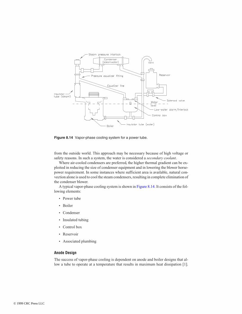
from the outside world. This approach may be necessary because of high voltage orsafety reasons. In such a system, the water is considered a secondary coolant.
Where air-cooled condensers are preferred, the higher thermal gradient can be ex-ploited in reducing the size of condenser equipment and in lowering the blower horse-power requirement. In some instances where sufficient area is available, natural con-vection alone is used to cool the steam condensers, resulting in complete elimination ofthe condenser blower.
A typical vapor-phase cooling system is shown in Figure 8.14. It consists of the fol-lowing elements:
• Power tube
• Boiler
• Condenser
• Insulated tubing
• Control box
• Reservoir
• Associated plumbing
Anode Design
The success of vapor-phase cooling is dependent on anode and boiler designs that al-low a tube to operate at a temperature that results in maximum heat dissipation [1].
Figure 8.14 Vapor-phase cooling system for a power tube.
© 1999 CRC Press LLC

The most common approach has been to incorporate thick vertical fins on the exteriorof the anode to achieve a radial temperature gradient on the surfaces submerged inwater. In this way, a hot spot does not cause instantaneous runaway of the tube; onlythe average fin temperature increases, and this merely shifts the temperature range toa somewhat higher level. The temperatures of the fins typically vary from approxi-mately 110°C at the tip to about 180°C at the root. With an average overall fin temper-ature of approximately 115°C, for example, the average transferred heat flux is on theorder of 60 W/cm2.
When operating at low dissipation levels, boiling takes place at the root of the fin.Increasing power density causes this boiling area to move out toward the end of the finuntil, at rated dissipation levels, boiling takes place on the outer half of the fins. Gooddesign dictates that the anode fin outer edge always remain at less than 125°C.
Anode shape is also important in assuring good cooling by breaking up the sheath ofvapor that might tend to form at the surfaces. To a point, the more complicated theshape, the more efficient the anode cooler. Horizontal slots often are milled into thevertical fins to provide more area and to break up bubbles. The more vigorous the boil-ing action, the lower the possibility that an insulating vapor sheath will form. One de-sign—known as the “pineapple”—carries this idea to the extreme, and incorporatessquare “knobs” all around the anode to provide dozens of heat-radiating surfaces. Themore conventional finned anode, however, is generally adequate and less costly to fab-ricate.
The holed anode is another popular design for lower power densities (up to 100W/cm2). In this design, a heavy cylindrical anode is made with vertical holes in the out-side wall. Vapor, formed by the boiling of water within the holes, is siphoned upwardthrough the holes to the top of the boiler. This type of cooler always operates below thecalefaction point and is used in smaller tube types. The concept is illustrated in Figure8.15.
Boiler
The boiler supports the power tube and contains the water used for cooling [1]. In ad-dition, it acts as the high-voltage anode connector. The boiler should be mounted sothat the axis of the tube is vertical. For effective cooling, tilt should be limited to lessthan 2° to ensure that the anode is covered with water and that the steam outlet is clear.Figure 8.16 shows a 4CV35,000A tetrode mounted in a boiler.
The anode flange of the tube must seal securely against the O-ring provided on theboiler. A locking flange presses the anode flange against the O-ring for a vapor-tightseal. The steam outlet at the top of the steam separation chamber on the boiler and thewater inlet at the bottom of the boiler are equipped with fittings for attaching the Py-rex-insulated tubing. A target to inhibit electrolytic action is provided in the inlet waterfitting.
In most cases the boiler is at a high potential relative to ground. Therefore, it must beelectrically insulated from the rest of the system. The boiler is mounted on insulators,and the steam and water connections are made through insulating tubing. Boilers can be
© 1999 CRC Press LLC

constructed with provisions for mounting multiple tubes in parallel. In such an arrange-ment, a single water inlet and steam outlet fitting typically would be used.
Common anode/boiler hardware is well suited to RF amplifiers operating up into theHF band, which typically use conventional tuned circuits. Operation in systems athigher frequencies, however, becomes more complicated than water cooling, and cer-
Figure 8.15 Cross section of a holed anode design for vapor-phase cooling.
Figure 8.16 A 4CV35,000A tetrode mountedin its boiler assembly. (Courtesy of Varian.)
© 1999 CRC Press LLC

tainly more complicated than air cooling. The cooling system in an air-cooled RF gen-erator does not interfere with the proper operation of the cavity; it is invisible to the cav-ity. Water cooling introduces some compromises and/or adjustments in the cavity,which can be readily overcome. Vapor-cooled tubes, however, require special design at-tention for successful use.
Insulating Tubing
The length of the steam and water insulating lines varies with individual installationrequirements, but will always be shorter than would be needed in a circulating watersystem [1]. The length of the insulating tubing is determined by the following consid-erations:
• The voltage to be applied to the tube anode
• Purity of the water
• Volume of returned cooling water
Control Box
The function of the control box is to monitor and adjust the water level in the boiler[1]. A typical box is shown in Figure 8.17. The control box, an airtight vessel contain-ing an overflow siphon and two float switches, also serves as a partial reservoir. Whenthe water level drops approximately 1/4 in below the recommended level, the firstswitch is closed. This signal may be used, at the same time, to activate a solenoid-con-trolled water valve to admit more distilled water from an external reservoir; it alsomay actuate a warning alarm.
Figure 8.17 Control box for a va-por-phase cooling system. (Courtesyof Varian.)
© 1999 CRC Press LLC

The second float switch is operated if the water level drops approximately 1/2 in be-low the optimum level. This would be tantamount to a water system failure; the switchwould be used to open the control circuit interlocks and remove power from the tube.
For the control box to perform its protective function properly, the water-level markmust be precisely in line with the water-level mark on the boiler. For electrical reasons,the control box generally is mounted some distance from the boiler, and therefore level-ing of the two components must be carefully checked during installation. Figure 8.18shows a cutaway drawing of a classic boiler and tube combination. Figure 8.19 is acutaway drawing of a control box, showing the position of the float switches and theoverflow pipe.
During extended operation, some quantity of water and steam being circulatedthrough the condenser will be lost. The amount is dependent on the size of the system.The water level in the boiler, therefore, will gradually drop. The use of the control boxas a reservoir minimizes this effect. In large or multiple-tube installations, an auxiliaryreservoir is connected to the control box to increase the ratio of stored water to circulat-ing water and steam. Where it may be necessary to operate multiple tubes at differentphysical elevations, individual control boxes are required. A multiple-tube system isshown in Figure 8.20.
Equalizer Line
For the control box to duplicate the same pressure conditions that exist in the boiler,the vapor-phase system must be fitted with an equalizer line [1]. This length of tubingconnects the steam side of the system with the top of the control box. As partial steam
Figure 8.18 Cutaway view of a boiler and tube combination.
© 1999 CRC Press LLC

pressure begins to build up in the boiler, the equalizer line allows this same pressureto appear in the control box. Although the steam pressure is low, less than 0.5 psiabove atmosphere, an error in the operation of the control box would be introducedunless the vessel were equalized.
The fitting used to connect the equalizer line to the steam outlet tube must be con-structed to prevent a venturi effect from developing because of the velocity of the vapor.This is best accomplished by directing an elbow within the adapter fitting toward theboiler, as shown in Figure 8.21.
Condenser
Both air-cooled and water-cooled condensers are available for vapor cooling systems[1]. Choose condensers with good reserve capabilities and low pressure drop. Air-and water-cooled condensers may be mounted in any position, provided they allowthe condensed water to flow freely by gravity to the boiler return line. Water must notbe allowed to stand in the condenser where it might cause back pressure to the enter-ing steam.
The condenser should be mounted above the level of the boiler(s) so that water willdrain from it to the boiler return line. Where it is necessary to mount the condenser at alower physical level than the system water level, an auxiliary pump must be used to re-
Figure 8.19 Cutaway view of a control box.
© 1999 CRC Press LLC

Figure 8.20 Typical four-tube vapor cooling system with a common water supply.
© 1999 C
RC
Press LL
C

turn water to the boiler. This arrangement is recommended for the “steam-out-the-bot-tom” boiler system, as illustrated in Figure 8.22.
Pressure Interlock
Most tube manufacturers recommend the use of a steam pressure interlock switch onthe steam or inlet side of the condenser [1]. This switch, set to about 0.5 lbs/in2, isused as a power interlock that senses abnormal steam pressure resulting from con-strictions in the condenser or piping.
Piping
Piping should be of copper or glass throughout the system [1]. The steam pipingshould be the same diameter as the Pyrex tube from the boiler. The size is dependenton the power level and the volume of generated steam, and it will range from 1-1/4 inat the 8 kW level to 6 in for the 250 kW level of dissipation. The steam path should beas direct as practical and must be sloped to prevent condensate from collecting at alow point where it might cause back pressure. All low spots should be drained back tothe inlet water line.
The diameter of water return piping from the condenser to the control box will varyfrom 3/4 to 1-3/4 in, depending again on the power level. This tubing should be thesame diameter as the boiler inlet water fitting. It also should be sloped so that water orvapor pockets are not allowed to form, and it must allow the condensate to return bygravity to the control box and the boiler. A vent to air on the outlet side of the condensershould be incorporated to maintain the water side of the system at atmospheric pres-sure. Provisions for draining the distilled water should be made at the lowest physicallevel of the system.
Figure 8.21 Cutaway view of a pressureequalizer fitting.
© 1999 CRC Press LLC

Figure 8.22 Typical four-tube vapor cooling system using “steam-out-the-bottom” boilers.
© 1999 C
RC
Press LL
C

The equalizer line also should be sloped from the adapter fitting on the steam line tothe top of the control box. This will allow the condensate to return to the control box.
Automatic Refilling System
Figure 8.23 shows a typical vapor cooling system with provisions to allow additionalwater into the control box [1]. An auxiliary reservoir is connected through a sole-noid-operated water valve to the controller. When water loss resulting from evapora-tion causes the water level in the boiler and the control box to drop about 1
4 in belownormal, the first float switch in the control box closes and actuates the solenoid-con-trolled valve to permit makeup water to enter the system. When the proper level is re-stored, the switch opens, the valve closes, and the flow of makeup water is stopped.
Alternative Vapor Cooling Systems
The systems described thus far are “classic” designs in which a separate tube, boiler,condenser, and level control box are used [1]. Variations on this basic scheme are nu-merous. One such alternative system, offered for use with large power tubes, utilizes a“steam-out-the-bottom” boiler. This configuration makes it possible to keep thesteam and water systems, plus the plumbing, below the tubes. This configuration of-ten simplifies the electrical design of the amplifier or oscillator. Figure 8.24 shows atypical boiler used in this cooling technique.
A small water pump circulates a continuous flow of water over a weir—or baffle—inthe boiler, maintaining a constant water level. Generated steam is forced under slight
Figure 8.23 Vapor cooling system incorporating a reservoir of distilled water.
© 1999 CRC Press LLC

pressure out the bottom of the boiler, through an insulator tube in the condenser. Waterfrom the condenser flows into the control box before being pumped back into the boiler.Protective devices include a water-flow interlock and water-level switch in the controlbox to ensure an adequate supply of coolant.
Maintenance
Maintenance problems associated with circulating water systems are practically elim-inated in a vapor cooling system [1]. As mentioned previously, systems can be de-signed to eliminate all rotating machinery or moving parts. Good engineering practicedoes, however, dictate periodic maintenance. The glass insulator tubes should be in-spected occasionally to be sure they contain no deposits that might cause high-voltageflashover. Water conductivity can be checked by measuring the dc resistance, as in atypical circulating water system. The water should be replaced if the dc resistancedrops below 1.0 MΩ-cm.
In practice, a vapor-cooled system will remain cleaner longer than a water-cooledsystem. In the vapor-cooled boiler, the water is continuously being redistilled, and onlypure water is introduced at the bottom of the boiler. Any contaminants will tend to re-main in the boiler itself, where they can be removed easily. The periods between equip-ment shutdown for draining and cleaning will be at least twice as long for a vapor cool-ing system because of this inherent self-cleaning action.
Each time a tube is removed or replaced, the rubber O-ring between the boiler andthe tube should be inspected and, if necessary, replaced. At the same time, the inside ofthe boiler and the control box can be inspected and cleaned as needed. The electrolytic
Figure 8.24 Cutaway view of a “steam-out-the-bottom” boiler.
© 1999 CRC Press LLC

target should be replaced whenever its metallic end is no longer visible in the inlet wa-ter line.
8.2.4 Temperature Measurements
Before completing any design employing power tubes, check temperatures in criticalareas, such as metal/ceramic seals and (except for water- and vapor-cooled types) theanode just above and below the cooling fins [1]. Another critical area on many me-dium and large tubes of coaxial design is the central part of the base, which is often re-cessed and may need special cooling provisions. Electrical contact to the tube termi-nals is usually by copper-beryllium collets, which should not exceed a temperature of150°C for any extended period of time. A number of manufacturers make tempera-ture-sensitive paints that are useful for such measurements.3 “Crayon-type” indicatorsare also available, in a wide range of temperatures. Conventional temperature measur-ing-techniques may be affected by the radio frequency energy concentrated at the tubeand nearby components. Furthermore, because all power tubes operate at high volt-age, there is danger of electric shock with directly connected devices.
When a temperature-sensitive paint or crayon is used for measurement, it must beremembered that many of the areas of concern are vacuum seals involving relativelythin metal. It is important, therefore, that the indicator material be noncorrosive.
Considering the importance of tube element temperatures, every design must beevaluated carefully. All power tubes carry an absolute maximum temperature rating forthe seals and envelope, and in the case of an external-anode forced-air-cooled tube, forthe anode core itself. Operation above the rated maximum can cause early tube failure.Where long life and consistent performance are important factors, it is normally desir-able to maintain tube temperatures comfortably below the rated maximum.
The equipment operator has the ultimate responsibility of making sure that thepower tubes used in the system are operating within specified ratings. Most currenttube designs use a ceramic envelope and an externally mounted anode or collector. Theonly visible sign of excessive temperature may be the cosmetic plating beginning todarken or turn black (oxidize). By then, significant damage may have occurred.
“Crayon” Temperature Measurement
When a crystalline solid is heated, a temperature will be reached at which the solidchanges sharply to a liquid [1]. This melting point has a definite, reproducible valuethat is virtually unaffected by ambient conditions that may cause errors in other tem-perature-sensing methods. For example, fusible temperature indicators are practicalin induction heating and in the presence of static electricity or ionized air around elec-tric equipment, where electronic means of measuring temperatures often function er-ratically.
3 Tempilaq is one such product (Tempil Division, Big Three Industrial Gas and EquipmentCo., South Plainfield, NJ).
© 1999 CRC Press LLC

The most popular type of fusible indicator is a temperature-sensitive stick closelyresembling a crayon, with a calibrated melting point. These crayon-type indicators aremade in 100 or so different specified temperature ratings in the range of 100 to 2500°F.Typically, each crayon has a temperature-indicating accuracy within 1 percent of its rat-ing. The workpiece to be tested is marked with the crayon. When the workpiece attainsthe predetermined melting point of the crayon, the mark instantly changes from a solidto a liquid phase (liquefies), indicating that the workpiece has reached that tempera-ture.
Under certain circumstances, premarking with crayon is not practical. This is thecase if one or more of the following is true:
• A prolonged heating period is experienced.
• The surface is highly polished and does not readily accept a crayon mark.
• The material being marked is one that gradually absorbs the liquid phase of thecrayon.
Note that a melted mark, upon cooling, will not solidify at the exact temperature atwhich it melted. Solidification of a melted crayon mark, therefore, cannot be relied onfor exact temperature indication.
Phase-Change Fluid
A phase-changing fluid, or fusible temperature-indicating lacquer, offers the greatestflexibility in temperature measurement of a power tube [1]. The lacquer-type fluidcontains a solid material of calibrated melting point suspended in an inert, volatile,nonflammable vehicle. As with crayon-type indicators, there are approximately 100different temperature ratings, covering a range from 100 to 2500°F. Accuracy is typi-cally within 1 percent of the specified value.
The lacquer is supplied in the proper consistency for brushing. If spraying or dip-ping is desirable as the mode of application, a thinner is available to alter the viscositywithout impairing the temperature-indicating accuracy.
Phase-changing lacquers often are used when a smooth or soft surface must betested, or in situations where the surface is not readily accessible for application of acrayon mark during the heating process. Within seconds after application, the lacquerdries to a dull matte finish, and it responds rapidly when the temperature to be indicatedis reached. The response delay of a lacquer mark is only a fraction of a second. Thistime can be reduced to milliseconds if a mark of minimal thickness is applied.
Upon reaching its rated temperature, the lacquer mark will liquefy. On subsequentcooling, however, the fluid will not revert to its original unmelted appearance but,rather, to a glossy or crystalline coating, which is evidence of its having reached the re-quired temperature. Temperature-indicating lacquers, upon cooling, will not resolidifyat the same temperature at which they melted.
If spraying of the phase-change lacquer is to be the sole means of application, the op-erator may find it more convenient to use an aerosol-packaged form of this material. An
© 1999 CRC Press LLC

aerosol phase-change temperature indicator is identical to the brush-on material in per-formance and interpretation.
The first commercial form of the fusible indicator was the pellet, which continues tobe useful in certain applications. Pellets are most frequently employed when extendedheating periods are involved, or where a greater bulk of indicator material is necessary.They are also useful when observations must be made from a distance and whenair-space temperatures are to be monitored.
Phase-change temperature-indicator pellets are available in flat, 7/16-in-diameter ×1/8-in-thick tablets. For special applications, miniature pellets, 1/8 in × 1/8 in, are alsoavailable. The range of 100 to 2500°F covered by the crayon and lacquer-type is, like-wise, covered by the pellets. Pellets with coverage extending to 3200°F also may be ob-tained.
Another variation of the phase-change indicator is the temperature-sensitive label.4
These self-adhesive-backed monitors consist of one or more heat-sensitive indicatorssealed under transparent heat-resistant windows. The centers of the indicator circlesturn from white to black at the temperature ratings shown on the label. The change toblack is irreversible, representing an absorption of the temperature-sensitive substanceinto its backing material. After registering the temperature history of the workpiece, theexposed monitor label can be removed and affixed to a service report to remain part of apermanent record.
Selection Process
Fusible temperature indicators and lacquers have at least three major advantages overother methods of determining surface temperature [1]:
• The temperature indications obtained are unquestionably those of the surface be-ing tested. It is not necessary to equilibrate a relatively massive probe with thesurface (a probe may conduct heat away from the region being tested), which re-quires the use of a correction factor to obtain the actual surface temperature.
• There is no delay in obtaining an indication. Because a mark left by a crayon or alacquer is of extremely small mass, it attains rapid equilibrium with the surface.There is no conduction of heat away from the surface, which would prolong re-sponse time and result in erroneously low temperature readings.
• The technique is simple and economical. Determination of surface temperatureby most other means requires technical competence and skill and, in some cases,sophisticated instrumentation. Accurate surface temperature readings can be ob-tained with fusible indicators and lacquers with little effort, training, and ex-pense.
4 Temp-Plate is one such product (Williams-Wahl Corp., Santa Monica, CA).
© 1999 CRC Press LLC

There are numerous instances, particularly in determining heat distribution in com-plex systems, in which the relative simplicity of fusible indicators and lacquers makessurface temperature investigations feasible.
8.2.5 Air-Handling System
All modern air-cooled PA tubes use an air-system socket and matching chimney forcooling [1]. The chimney is designed to be an integral part of the tube cooling system.Operation without the chimney may significantly reduce airflow through the tube andresult in overdissipation of the device. It also is possible that operation without theproper chimney could damage other components in the circuit because of excessiveradiated heat. Normally, the tube socket is mounted in a pressurized compartment sothat cooling air passes through the socket and is guided to the anode cooling fins, asillustrated in Figure 8.25.
Cooling of the socket assembly is important for proper cooling of the tube base andfor cooling the contact rings of the tube itself. The contact fingers used in the collet as-sembly of a socket typically are made of beryllium copper. If subjected to temperaturesabove 150°C for an extended period of time, the beryllium copper will lose its temper(springy characteristic) and will no longer make good contact with the base rings of thedevice. In extreme cases, this type of socket problem may lead to arcing, which canburn through the metal portion of the tube base ring. Such an occurrence ultimatelymay lead to catastrophic failure of the device because of a loss of the vacuum envelope.Other failure modes for a tube socket include arcing between the collet and tube ring,which can weld a part of the socket and tube together. The result is failure of both thetube and the socket.
8.3 Operating EnvironmentLong-term reliability of a power vacuum tube requires regular attention to the operat-ing environment. Periodic tests and preventive maintenance are important compo-nents of this effort. Optimum performance of the cooling system can be achieved onlywhen all elements of the system are functioning properly.
8.3.1 Air-Handling System
The temperature of the intake air supply is a parameter that is usually under the con-trol of the end user. The preferred cooling air temperature is typically no higher than75°F, and no lower than the room dew point. The air temperature should not vary be-cause of an oversized air-conditioning system or because of the operation of otherpieces of equipment at the facility. Monitoring the PA tube exhaust stack temperatureis an effective method of evaluating overall RF system performance. This can be eas-ily accomplished. It also provides valuable data on the cooling system and final stagetuning.
Another convenient method for checking the efficiency of the transmitter coolingsystem over a period of time involves documenting the back pressure that exists within
© 1999 CRC Press LLC

the PA cavity. This measurement is made with a manometer, a simple device that isavailable from most heating, ventilation, and air-conditioning (HVAC) suppliers. Theconnection of a simplified manometer to a transmitter PA output compartment is illus-trated in Figure 8.26.
By charting the manometer readings, it is possible to accurately measure the perfor-mance of the transmitter cooling system over time. Changes resulting from the buildupof small dust particles (microdust) may be too gradual to be detected except throughback-pressure charting. Deviations from the typical back-pressure value, either higheror lower, could signal a problem with the air-handling system. Decreased PA input oroutput compartment back pressure could indicate a problem with the blower motor oran accumulation of dust and dirt on the blades of the blower assembly. Increased backpressure, on the other hand, could indicate dirty PA tube anode cooling fins (for the in-put compartment case) or a buildup of dirt on the PA exhaust ducting (for the outputcompartment case). Either condition is cause for concern. A system suffering from re-
Figure 8.25 Airflow system for an air-cooled power tube.
© 1999 CRC Press LLC

duced air pressure into the PA compartment must be serviced as soon as possible. Fail-ure to restore the cooling system to proper operation may lead to premature failure ofthe PA tube or other components in the input or output compartments. Cooling prob-lems do not improve with time; they always get worse.
Failure of the PA compartment air-interlock switch to close reliably may be an earlyindication of impending trouble in the cooling system. This situation could be causedby normal mechanical wear or vibration of the switch assembly, or it may signal that thePA compartment air pressure has dropped. In such a case, documentation of manome-ter readings will show whether the trouble is caused by a failure of the air pressureswitch or a decrease in the output of the air-handling system.
Figure 8.26 A manometer device used for measuring back pressure in the PA compart-ment of an RF generator.
© 1999 CRC Press LLC

8.3.2 Air Cooling System Design
Cooling system performance in an RF generator is not necessarily related to airflowvolume. The cooling capability of air is a function of its mass, not its volume. The de-signer must determine an appropriate airflow rate within the equipment and establishthe resulting resistance to air movement. A specified static pressure that should bepresent within the ducting of the transmitter can be a measure of airflow. For anygiven combination of ducting, filters, heat sinks, RFI honeycomb shielding, tubes,tube sockets, and other elements in the transmitter, a specified system resistance toairflow can be determined. It is important to realize that any changes in the position ornumber of restricting elements within the system will change the system resistanceand, therefore, the effectiveness of the cooling. The altitude of operation is also a con-sideration in cooling system design. As altitude increases, the density (and coolingcapability) of air decreases. A calculated increase in airflow is required to maintainthe cooling effectiveness that the system was designed to achieve.
Figure 8.27 shows a typical high-power transmitter plant. The building is oriented sothat the cooling activity of the blowers is aided by normal wind currents during the sum-mer months. Air brought in from the outside for cooling is filtered in a hooded air-in-take assembly. The building includes a heater and air conditioner.
Figure 8.27 A typical heating and cooling arrangement for a high-power transmitter in-stallation. Ducting of PA exhaust air should be arranged so that it offers minimum resis-tance to airflow.
© 1999 CRC Press LLC

The layout of a transmitter room HVAC system can have a significant impact on thelife of the PA tube(s) and the ultimate reliability of the RF generator. Air intake and out-put ports must be designed with care to avoid airflow restrictions and back-pressureproblems. This process, however, is not as easy as it may seem. The science of airflow iscomplex and generally requires the advice of a qualified HVAC consultant.
To help illustrate the importance of proper cooling system design and the real-worldproblems that some facilities have experienced, consider the following examples takenfrom actual case histories:
Case 1
A fully automatic building ventilation system (Figure 8.28) was installed to maintainroom temperature at 20°C during the fall, winter, and spring. During the summer,however, ambient room temperature would increase to as much as 60°C. A field sur-vey showed that the only building exhaust route was through the transmitter. There-fore, air entering the room was heated by test equipment, people, solar radiation onthe building, and radiation from the transmitter itself before entering the transmitter.The problem was solved through the addition of an exhaust fan (3000 cfm). The 1 hpfan lowered room temperature by 20°C.
Case 2
A simple remote installation was constructed with a heat-recirculating feature for thewinter (Figure 8.29). Outside supply air was drawn by the transmitter cooling systemblowers through a bank of air filters, and hot air was exhausted through the roof. A
Figure 8.28 Case study in which excessive summertime heating was eliminatedthrough the addition of a 1 hp exhaust blower to the building.
© 1999 CRC Press LLC

small blower and damper were installed near the roof exit point. The damper allowedhot exhaust air to blow back into the room through a tee duct during the wintermonths. For summer operation, the roof damper was switched open and the roomdamper closed. For winter operation, the arrangement was reversed. The facility, how-ever, experienced short tube life during winter operation, even though the ambientroom temperature during winter was not excessive.
The solution involved moving the roof damper 12 ft down to just above the tee. Thiseliminated the stagnant “air cushion” above the bottom heating duct damper and signif-icantly improved airflow in the region. Cavity back pressure was, therefore, reduced.With this relatively simple modification, the problem of short tube life disappeared.
Case 3
An inconsistency regarding test data was discovered within a transmitter manufac-turer’s plant. Units tested in the engineering lab typically ran cooler than those at themanufacturing test facility. Figure 8.30 shows the test station difference, a 4-ft ex-haust stack that was used in the engineering lab. The addition of the stack increased
Figure 8.29 Case study in which excessive back pressure to the PA cavity was experi-enced during winter periods, when the rooftop damper was closed. The problem waseliminated by repositioning the damper as shown.
© 1999 CRC Press LLC

airflow by up to 20 percent because of reduced air turbulence at the output port, re-sulting in a 20°C decrease in tube temperature.
These examples point out how easily a cooling problem can be caused during HVACsystem design. All power delivered to the transmitter either is converted to RF energyand sent to the antenna or becomes heated air (or water). Proper design of a cooling sys-tem, therefore, is a part of transmitter installation that should not be taken lightly.
8.3.3 Site Design Guidelines
There are any number of physical plant designs that will provide for reliable operationof high-power RF systems [3]. One constant, however, is the requirement for tighttemperature control. Cooling designs can be divided into three broad classifications:
• Closed site design
• Open site design
• Hybrid design
If the equipment user is to provide adequately for hot air exhaust and fresh air intake,the maximum and minimum environmental conditions in which the equipment will op-
Figure 8.30 Case study in which air turbulence at the exhaust duct resulted in reducedairflow through the PA compartment. The problem was eliminated by adding a 4-ft ex-tension to the output duct.
© 1999 CRC Press LLC

erate must be known. In addition, the minimum cooling requirements of the equipmentmust be provided by the manufacturer. The following parameters should be considered:
• Site altitude
• Maximum expected outside air temperature
• Minimum expected outside air temperature
• Total airflow through the transmitter
• Air temperature rise through the transmitter
• Air exhaust area
Keep in mind that the recommended cooling capacity for a given RF system appliesonly to cooling the transmitter; any additional cooling load in the building must be con-sidered separately when selecting the air system components. The transmitter exhaustshould not be the only exhaust port in the room because heat from the peripheral equip-ment would then be forced to go out through the transmitter.
The sensible-heat load, then, is the sum of all additional heat loads, including:
• Solar radiation
• Heat gains from equipment and lights
• Heat gains from personnel in the area that is to be cooled
Closed Site Design
Figure 8.31 illustrates a site layout that works well in most climates, as long as thetransmitter is small and the building is sealed and well insulated [3]. In fact, thisclosed configuration will ensure the longest possible transmitter life and lowest main-tenance cost. No outside air laden with moisture and contaminants circulates throughthe transmitter.
At sites using this arrangement, it has been observed that periodic transmitter clean-ing is seldom required. In a typical closed system, the air conditioner is set to cool whenthe room temperature reaches 75 to 80°F. The closed system also uses a louvered emer-gency intake blower, which is set by its own thermostat to pull in outside air if the roomtemperature reaches excessive levels (above 90°F). This blower is required in a closedconfiguration to prevent the possibility of thermal runaway if the air conditioner fails.Without such an emergency ventilation system, the transmitter would recirculate itsown heated air, further heating the room. System failure probably would result.
During winter months, the closed system is self-heating (unless the climate is harsh,or the transmitter power output is low), because the transmitter exhaust is not ductedoutside but simply empties into the room. Also during these months, the emergency in-take blower can be used to draw cold outside air into the room instead of using the airconditioner, although this negates some of the cleanliness advantages inherent to theclosed system.
© 1999 CRC Press LLC

An exhaust blower should not be substituted for an intake blower, because positiveroom pressure is desired for venting the room. This ensures that all air in the buildinghas passed through the intake air filter. Furthermore, the louvered emergency exhaustvent(s) should be mounted high in the room, so that hot air is pushed out of the buildingfirst.
The closed system usually makes economic sense only if the transmitter exhaustheat load is relatively small.
Periodic maintenance of a closed system involves the following activities:
• Checking and changing the air conditioner filter periodically
• Cleaning the transmitter air filter as needed
• Checking that the emergency vent system works properly
• Keeping the building sealed from insects and rodents
Open Site Design
Figure 8.32 depicts a site layout that is the most economical to construct and operate[3]. The main attribute of this approach is that the transmitter air supply is not heatedor cooled, resulting in cost savings. This is not a closed system; outdoor air is pumpedinto the transmitter room through air filters. The transmitter then exhausts the hot air.If the duct work is kept simple and the transmitter has a dedicated exhaust port, such adirect exhaust system works adequately. Many transmitters do not lend themselves to
Figure 8.31 Closed site ventilation design, with a backup inlet/outlet system.
© 1999 CRC Press LLC

a direct exhaust connection, however, and a hood mounted over the transmitter may berequired to collect the hot air, as illustrated in Figure 8.33. With a hooded arrange-ment, it may be necessary to install a booster fan in the system, typically at the wall orroof exit, to avoid excessive back pressure.
When building an open air-circulation system, there are some important additionalconsiderations. The room must be positively pressurized so that only filtered air, whichhas come through the intake blower and filter, is available to the transmitter. With a neg-atively pressurized room, air will enter through every hole and crack in the building,and will not necessarily be filtered. Under negative pressure, the transmitter bloweralso will have to work harder to exhaust air.
The intake blower should be a “squirrel-cage” type rather than a fan type. A fan ismeant to move air within a pressurized environment; it cannot compress the air. Asquirrel-cage blower will not only move air, but also will pressurize the area into whichthe air is directed. Furthermore, the intake air blower must be rated for more cubic feetper minute (cfm) airflow than the transmitter will exhaust outside. A typical 20 kW FMbroadcast transmitter, for example, will exhaust 500 cfm to 1000 cfm. A blower of 1200cfm, therefore, would be an appropriate size to replenish the transmitter exhaust andpositively pressurize the room.
In moderate and warm climates, the intake blower should be located on a north-fac-ing outside wall. If the air intake is on the roof, it should be elevated so that it does notpick up air heated by the roof surface.
Figure 8.32 Open site ventilation design, using no air conditioner.
© 1999 CRC Press LLC

High-quality pleated air filters are recommended. Home-style fiberglass filters arenot sufficient. Local conditions may warrant using a double filtration system, withcoarse and fine filters in series.
Secure the advice of a knowledgeable HVAC shop when designing filter boxes. Fora given cfm requirement, the larger the filtration area, the lower the required air velocitythrough the filters. This lower velocity results in better filtration than forcing more airthrough a small filter. In addition, the filters will last longer. Good commercial filtra-tion blowers designed for outdoor installation are available from industrial supplyhouses and are readily adapted to RF facility use.
The transmitter exhaust may be ducted through a nearby wall or through the roof.Avoid ducting straight up, however. Many facilities have suffered water damage totransmitters in such cases because of the inevitable deterioration of roofing materials.Normally, ducting the exhaust through an outside wall is acceptable. The duct worktypically is bent downward a foot or two outside the building to keep direct wind fromcreating back pressure in the exhaust duct. Minimize all bends in the duct work. If a 90°bend must be made, it should be a large-radius bend with curved helper vanes inside theduct to minimize turbulence and back pressure. A 90° L- or T-bend is not recom-mended, unless oversized and equipped with internal vanes to assist the turning airflow.
For moderate and cool climates, an automatic damper can be employed in the ex-haust duct to direct a certain amount of hot exhaust air back into the transmitter build-
Figure 8.33 Transmitter exhaust-collection hood.
© 1999 CRC Press LLC

ing as needed for heating. This will reduce outside air requirements, providing clean,dry, heated air to the transmitter during cold weather.
Hybrid Design
Figure 8.34 depicts a hybrid site layout that is often used for high-power transmittersor sites supporting multiple transmitters [3]. As with the layout in Figure 8.32, theroom is positively pressurized with clean, filtered air from the outside. A portion ofthis outside air is then drawn through the air conditioner for cooling before delivery tothe transmitter area. Although not all of the air in the room goes through the air condi-tioner, enough does to make a difference in the room temperature. In humid areas,much of the moisture is removed by the air conditioner. The transmitter exhaust is di-rected outside.
Such a hybrid system is often the choice for larger transmitter sites where a closedsystem would prove too costly, but an unconditioned system would run excessively hotduring the summer months.
Some closed or hybrid systems use two parallel air conditioners. Most of the time,only one is in use. The thermostats of the units are staggered so that if one cannot keepthe air below the ideal operating point, the other will turn on to assist.
Figure 8.34 Hybrid site ventilation design, using an air conditioner in addition to filteredoutside air.
© 1999 CRC Press LLC

8.3.4 Water/Vapor Cooling System Maintenance
The cooling system is vital to any RF generator. In a klystron-based unit, for example,the cooling system may dissipate a large percentage of the input ac power in the formof waste heat in the collector. Pure, distilled water should be used. Deionized water isrequired unless the isolation of high voltages is unnecessary, as in the case of the col-lector of a klystron (the collector typically operates at or near ground potential).
Any impurities in the cooling system water eventually will find their way into thewater jacket and cause corrosion of the plate or collector. It is essential to use high-pu-rity water with low conductivity, and to replace the water in the cooling system asneeded. Efficient energy transfer from the heated surface into the water is necessary forlong vacuum tube life. Oil, grease, soldering flux residue, and pipe sealant containingsilicone compounds must be excluded from the cooling system. This applies to both va-por- and liquid-conduction cooling systems, although it is usually more critical in thevapor-phase type. The sight glass in a vapor-phase water jacket provides a convenientcheckpoint for coolant condition.
In general, greater flows and greater pressures are inherent in liquid-cooled vs. va-por-phase systems, and, when a leak occurs, large quantities of coolant can be lost be-fore the problem is discovered. The condition of gaskets, seals, and fittings, therefore,should be checked regularly. Many liquid-cooled tubes use a distilled water and ethyl-ene glycol mixture. (Do not exceed a 50:50 mix by volume.) The heat transfer of themixture is lower than that of pure water, requiring the flow to be increased, typically by25 percent. Greater coolant flow suggests closer inspection of the cooling system afteradding the glycol.
The action of heat and air on ethylene glycol causes the formation of acidic products.The acidity of the coolant can be checked with litmus paper. Buffers can be added to theglycol mixture. Buffers are alkaline salts that neutralize acid forms and prevent corro-sion. Because they are ionizable chemical salts, the buffers cause the conductivity ofthe coolant to increase. Consult the power tube manufacturer before adding buffers.
The following general guidelines are recommended for power tube cooling systems:
• The resistivity of the water must be maintained above the minimum level estab-lished by the power tube manufacturer. Although recommended values vary,generally speaking, resistivity should be maintained at or above 1 MΩ-cm (at30ºC) for power tubes operating at a high-voltage, referenced to ground. A resis-tivity value of 30 kΩ-cm or greater (at 30ºC) is usually sufficient for tubes whosecollector operates at or near ground potential (such as a klystron).
• The pH factor must be within the range of 6.0 to 8.0.
• The particulate matter size must not be greater than 50 microns (325 mesh).
• The inlet water temperature must not exceed 70°C, and this temperature shouldbe regulated to ±5ºC.
When the water in the cooling system fails to satisfy any one of these requirements,prompt action is necessary to correct the deficiency. If the water is contaminated, thesystem must be flushed and replaced with clean water.
© 1999 CRC Press LLC

Tests for Purity
The recommended method for measuring resistivity, pH, and particulate matter is byuse of laboratory instruments. However, the following simple tests should providesufficient information to determine the general condition of the coolant.
• The appearance of the water is a good general indicator of coolant condition. Ifthe water looks turbid or tastes or smells brackish, it is good practice to change thewater and flush the system.
• The pH factor is easily checked by using pH paper or litmus paper. Sold under avariety of trade names, pH paper is available at laboratory supply stores. Direc-tions for use usually are printed on the package.
• Particulate matter and impurities can be checked by using the “foaming test” (de-scribed in the next section).
• Resistivity can be measured accurately with a resistance bridge. Generally speak-ing, if the water does not pass the foaming test, the resistivity will be low as well.
Foaming Test for Water Purity
One of the many factors affecting the life and operating efficiency of vapor-cooledtubes is the purity of the water in the cooling system. If impurities are present, foam-ing may occur that will inhibit heat transfer, thereby lowering the cooling efficiencyof the system. The impurities that most frequently produce foaming are:
• Cleaning-compound residue
• Detergents
• Joint-sealing compounds
• Oily rust preventives in pumps and other components
• Valve-stem packing
• Impurities in tap water
Tests should be conducted periodically to confirm the quality of the coolant in a va-por-phase system. Conduct such tests after each water change, system cleaning, ormodification. The following items are required:
• A 1/2-in × 4-in glass test tube with rubber stopper
• A 1-pint glass or polypropylene bottle with cap
The procedure is as follows:
• Fill the cooling system with water, and circulate it until thoroughly mixed (about30 minutes).
• Drain a sample of water into the bottle, and cool to room temperature.
© 1999 CRC Press LLC

• If the water sample stands for more than 1 hour, slowly invert the capped bottleabout 10 times. Avoid shaking the bottle because this will create air bubbles in thewater. (When the water is static, foaming impurities tend to collect at the surface.This step mixes the sample without generating foam.)
• Using the sample water, rinse the test tube and stopper three times.
• Fill the test tube to the halfway mark with the sample water.
• Shake the test tube vigorously for 15 s.
• Let the sample stand for 15 s.
• Observe the amount of foam remaining on top of the water and compare it withthe drawings shown in Figure 8.35.
A completely foam-free water surface and test tube, as illustrated in (a), indicates nofoam-producing impurities. If the water surface and test tube wall are partially coveredwith foam, but a circle of clear water appears in the center, the impurity level is tempo-rarily acceptable (b). A second test should be made in about one week. If the foam layercompletely bridges the inside of the test tube (c), the system should be flushed andcleaned.
8.4 References1. Laboratory Staff, The Care and Feeding of Power Grid Tubes, Varian Associates,
San Carlos, CA, 1984.2. Besch, David F., “Thermal Properties,” in The Electronics Handbook, Jerry C.
Whitaker (ed.), CRC Press, Boca Raton, FL, pp. 127–134, 1996.
Figure 8.35 Results of the “foaming test” for water purity: (a) pure sample, (b) samplethat is acceptable on a short-term basis, (c) unacceptable sample.
(a) (b) (c)
© 1999 CRC Press LLC

3. Harnack, Kirk, “Airflow and Cooling in RF Facilities,” Broadcast Engineering,Intertec Publishing, Overland Park, KS, pp. 33–38, November 1992.
8.5 Bibliography“Cleaning and Flushing Klystron Water and Vapor Cooling Systems,” Application En-
gineering Bulletin no. AEB-32, Varian Associates, Palo Alto, CA, February 1982.Crutchfield, E. B. (ed.), NAB Engineering Handbook, 8th Ed., National Association of
Broadcasters, Washington, DC, pp. 547–550, 1992.“Foaming Test for Water Purity,” Application Engineering Bulletin no. AEB-26,
Varian Associates, Palo Alto, CA, September 1971.Harnack, Kirk, “Airflow and Cooling in RF Facilities,” Broadcast Engineering,
Intertec Publishing, Overland Park, KS, pp. 33–38, November 1992.Harper, Charles A., Electronic Packaging and Interconnection Handbook,
McGraw-Hill, New York, NY, 1991.“High Power Transmitting Tubes for Broadcasting and Research,” Philips Technical
Publication, Eindhoven, the Netherlands, 1988.Integral Cavity Klystrons for UHF-TV Transmitters, Varian Associates, Palo Alto,
CA.Kimmel, E., “Temperature Sensitive Indicators: How They Work, When to Use
Them,” Heat Treating, March 1983.“Power Grid Tubes for Radio Broadcasting,” Thomson-CSF Publication #DTE-115,
Thomson-CSF, Dover, NJ, 1986.“Protecting Integral-Cavity Klystrons Against Water Leakage,” Technical Bulletin no.
3834, Varian Associates, Palo Alto, CA, July 1978.“Temperature Measurements with Eimac Power Tubes,” Application Bulletin no. 20,
Varian Associates, San Carlos, CA, January 1984.“Water Purity Requirements in Liquid Cooling Systems,” Application Bulletin no. 16,
Varian Associates, San Carlos, CA, July 1977.“Water Purity Requirements in Water and Vapor Cooling Systems,” Application Engi-
neering Bulletin no. AEB-31, Varian Associates, Palo Alto, CA, September 1991.Whitaker, Jerry C., Maintaining Electronic Systems, CRC Press, Boca Raton, FL,
1992.Whitaker, Jerry C., Radio Frequency Transmission Systems: Design and Operation,
McGraw-Hill, New York, NY, 1990.Wozniak, Joe, “Using Tetrode Power Amplifiers in High Power UHF-TV Transmit-
ters,” NAB 1992 Broadcast Engineering Conference Proceedings, National Associ-ation of Broadcasters, Washington, DC, pp. 209–211, 1992.
© 1999 CRC Press LLC

Whitaker, Jerry C. “Chapter 9 – Reliability Considerations” Power Vacuum Tubes Handbook 2nd Edition.Ed. Jerry C. WhitakerBoca Raton: CRC Press LLC, 2000
© 1999 CRC Press LLC

Chapter
9Reliability Considerations
9.1 IntroductionThe ultimate goal of any design engineer or maintenance department is zero down-time. This is an elusive goal, but one that can be approximated by examining the vul-nerable areas of plant operation and taking steps to prevent a sequence of events thatcould result in system failure. In cases where failure prevention is not practical, a reli-ability assessment should encompass the stocking of spare parts, circuit boards, oreven entire systems. A large facility may be able to cost-justify the purchase ofbackup gear that can be used as spares for the entire complex. Backup hardware is ex-pensive, but so is downtime. Because of the finite lifetime of power vacuum tubes,these considerations are of special significance.
Failures can, and do, occur in electronic systems. The goal of product quality assur-ance at every step in the manufacturing and operating chain is to ensure that failures donot produce a systematic or repeatable pattern. The ideal is to eliminate failures alto-gether. Short of that, the secondary goal is to end up with a random distribution of fail-ure modes. This indicates that the design of the system is fundamentally optimized andthat failures are caused by random events that cannot be predicted. In an imperfectworld, this is often the best that end users can hope for. Reliability and maintainabilitymust be built into products or systems at every step in the design, construction, andmaintenance process. They cannot be treated as an afterthought.
9.1.1 Terminology
To understand the principles of reliability engineering, the following basic terms mustbe defined:
• Availability. The probability that a system subject to repair will operate satisfac-torily on demand.
• Average life. The mean value for a normal distribution of product or componentlives. This term is generally applied to mechanical failures resulting from“wear-out.”
© 1999 CRC Press LLC

• Burn-in. The initially high failure rate encountered when a component is placedon test. Burn-in failures usually are associated with manufacturing defects andthe debugging phase of early service.
• Defect. Any deviation of a unit or product from specified requirements. A unit orproduct may contain more than one defect.
• Degradation failure. A failure that results from a gradual change, over time, inthe performance characteristics of a system or part.
• Downtime. Time during which equipment is not capable of doing useful workbecause of malfunction. This does not include preventive maintenance time.Downtime is measured from the occurrence of a malfunction to its correction.
• Failure. A detected cessation of ability to perform a specified function or func-tions within previously established limits. A failure is beyond adjustment by theoperator by means of controls normally accessible during routine operation of thesystem.
• Failure mode and effects analysis (FMEA). An iterative documented processperformed to identify basic faults at the component level and determine their ef-fects at higher levels of assembly.
• Failure rate. The rate at which failure occurs during an interval of time as a func-tion of the total interval length.
• Fault tree analysis (FTA). An iterative documented process of a systematic na-ture performed to identify basic faults, determine their causes and effects, and es-tablish their probabilities of occurrence.
• Lot size. A specific quantity of similar material or a collection of similar unitsfrom a common source; in inspection work, the quantity offered for inspectionand acceptance at any one time. This may be a collection of raw material, parts,subassemblies inspected during production, or a consignment of finished prod-ucts to be sent out for service.
• Maintainability. The probability that a failure will be repaired within a specifiedtime after it occurs.
• Mean time between failure (MTBF). The measured operating time of a singlepiece of equipment divided by the total number of failures during the measuredperiod of time. This measurement normally is made during that period betweenearly life and wear-out failures.
• Mean time to repair (MTTR). The measured repair time divided by the totalnumber of failures of the equipment.
• Mode of failure. The physical description of the manner in which a failure occursand the operating condition of the equipment or part at the time of the failure.
• Part failure rate. The rate at which a part fails to perform its intended function.
© 1999 CRC Press LLC

• Quality assurance (QA). All those activities, including surveillance, inspection,control, and documentation, aimed at ensuring that a product will meet its perfor-mance specifications.
• Reliability. The probability that an item will perform satisfactorily for a speci-fied period of time under a stated set of use conditions.
• Reliability growth. Actions taken to move a hardware item toward its reliabilitypotential, during development, subsequent manufacturing, or operation.
• Reliability predictions. Compiled failure rates for parts, components, subas-semblies, assemblies, and systems. These generic failure rates are used as basicdata to predict a value for reliability.
• Sample. One or more units selected at random from a quantity of product to rep-resent that product for inspection purposes.
• Sequential sampling. Sampling inspection in which, after each unit is inspected,the decision is made to accept, reject, or inspect another unit. (Note: Sequentialsampling as defined here is sometimes called unit sequential sampling or multiplesampling.)
• System. A combination of parts, assemblies, and sets joined together to perform aspecific operational function or functions.
• Test to failure. Testing conducted on one or more items until a predeterminednumber of failures have been observed. Failures are induced by increasing elec-trical, mechanical, and/or environmental stress levels, usually in contrast to lifetests, in which failures occur after extended exposure to predetermined stress lev-els. A life test can be considered a test to failure using age as the stress.
9.2 Quality AssuranceElectronic component and system manufacturers design and implement quality assur-ance procedures for one fundamental reason: Nothing is perfect. The goal of a QAprogram is to ensure, for both the manufacturer and the customer, that all but somesmall, mutually acceptable percentage of devices or systems shipped will be as closeto perfection as economics and the state of the art allow. There are tradeoffs in thisprocess. It would be unrealistic, for example, to perform extensive testing to identifypotential failures if the cost of that testing exceeded the cost savings that would be re-alized by not having to replace the devices later in the field.
The focal points of any QA effort are quality and reliability. These terms are not syn-onymous. They are related, but they do not provide the same measure of a product:
• Quality is the measure of a product’s performance relative to some establishedcriteria.
• Reliability is the measure of a product’s life expectancy.
© 1999 CRC Press LLC

Stated from a different perspective, quality answers the question of whether the prod-uct meets applicable specifications now; reliability answers the question of how longthe product will continue to meet its specifications.
9.2.1 Inspection Process
Quality assurance for components normally is performed through sampling ratherthan through 100 percent inspection. The primary means used by QA departments forcontrolling product quality at the various processing steps include:
• Gates. A mandatory sampling of every lot passing through a critical productionstage. Material cannot move on to the next operation until QA has inspected andaccepted the lot.
• Monitor points. A periodic sampling of some attribute of the component. QA per-sonnel sample devices at a predetermined frequency to verify that machines andoperators are producing material that meets preestablished criteria.
• Quality audit. An audit carried out by a separate group within the QA department.This group is charged with ensuring that all production steps throughout the man-ufacturer’s facility are in accordance with current specifications.
• Statistical quality control. A technique, based on computer modeling, that incor-porates data accumulated at each gate and monitor point to construct statisticalprofiles for each product, operation, and piece of equipment within the plant.Analysis of this data over time allows QA engineers to assess trends in productperformance and failure rates.
Quality assurance for a finished subassembly or system may range from a simplego/no-go test to a thorough operational checkout that may take days to complete.
9.2.2 Reliability Evaluation
Reliability prediction is the process of quantitatively assessing the reliability of acomponent or system during development, before large-scale fabrication and fieldoperation. During product development, predictions serve as a guide by which designalternatives can be judged for reliability. To be effective, the prediction techniquemust relate engineering variables to reliability variables.
A prediction of reliability is obtained by determining the reliability of each criticalitem at the lowest system level and proceeding through intermediate levels until an esti-mate of overall reliability is obtained. This prediction method depends on the availabil-ity of accurate evaluation models that reflect the reliability of lower-level components.Various formal prediction procedures are used, based on theoretical and statistical con-cepts.
© 1999 CRC Press LLC

Parts-Count Method
Although the parts-count method does not relate directly to vacuum tube design, it isworthwhile to discuss the technique briefly in the context of overall system reliability.It is fair to point out that this technique has considerable validity when comparisonsof vacuum tube vs. solid-state amplifier designs are being considered. To achievehigh power levels, far more individual components are necessary for a solid-state de-sign than for a vacuum tube-based system
The parts-count approach to reliability prediction provides an estimate of reliabilitybased on a count by part type (ICs, transistors, vacuum tube devices, resistors, capaci-tors, and other components). This method is useful during the early design stage of aproduct, when the amount of available detail is limited. The technique involves count-ing the number of components of each type, multiplying that number by a generic fail-ure rate for each part type, and summing the products to obtain the failure rate of eachfunctional circuit, subassembly, assembly, and/or block depicted in the system block di-agram. The parts-count method is useful in the design phase because it provides rapidestimates of reliability, permitting assessment of the feasibility of a given concept.
Stress-Analysis Method
The stress-analysis technique is similar to the parts-count method, but utilizes a de-tailed parts model plus calculation of circuit stress values for each part before deter-mining the failure rate. Each part is evaluated in its electric circuit and mechanical as-sembly application based on an electrical and thermal stress analysis. After part fail-ure rates have been established, a combined failure rate for each functional block isdetermined.
9.2.3 Failure Analysis
Failure mode and effects analysis can be performed with data taken from actual fail-ure modes observed in the field, or from hypothetical failure modes derived from oneof the following:
• Design analysis
• Reliability prediction activities
• Experience with how specific parts fail
In the most complete form of FMEA, failure modes are identified at the componentlevel. Failures are induced analytically into each component, and failure effects areevaluated and noted, including the severity and frequency (or probability) of occur-rence. Using this approach, the probability of various system failures can be calcu-lated, based on the probability of lower-level failure modes.
Fault tree analysis is a tool commonly used to analyze failure modes found duringdesign, factory test, or field operations. The approach involves several steps, includingthe development of a detailed logic diagram that depicts basic faults and events that canlead to system failure and/or safety hazards. These data are used to formulate corrective
© 1999 CRC Press LLC

suggestions that, when implemented, will eliminate or minimize faults considered crit-ical. An example FTA chart is shown in Figure 9.1.
9.2.4 Standardization
Standardization and reliability go hand in hand. Standardization of electronic compo-nents began with military applications in mind; the first recorded work was per-formed by the U.S. Navy with vacuum tubes. The navy recognized that some controlat the component level was essential to the successful incorporation of electronicsinto naval systems.
Standardization and reliability are closely related, although there are many aspectsof standardization whose reliability implications are subtle. The primary advantages ofstandardization include:
• Total product interchangeability. Standardization ensures that products of thesame part number provide the same physical and electrical characteristics. Therehave been innumerable instances of a replacement device bearing the same partnumber as a failed device, but not functioning identically to it. In many cases, thedifferences in performance were so great that the system would not function at allwith the new device.
• Consistency and configuration control. Component manufacturers constantly re-define their products to improve yields and performance. Consistency and con-figuration control assure the user that product changes will not affect theinterchangeability of the part.
• Efficiencies of volume production. Standardization programs usually result inproduction efficiencies that reduce the costs of parts, relative to components withthe same level of reliability screening and control.
• Effective spares management. The use of standardized components makes thestocking of spare parts a much easier task. This aspect of standardization is not aminor consideration. For example, the costs of placing, expediting, and receivingmaterial against one Department of Defense purchase order may range from $300to $1100. Accepting the lowest estimate, the conversion of 10 separate part num-bers to one standardized component could effect immediate savings of $3000 justin purchasing and receiving costs.
• Multiple product sources. Standardization encourages second-sourcing. Multi-ple sources help hold down product costs and encourage manufacturers to strivefor better product performance.
9.3 Reliability AnalysisThe science of reliability and maintainability matured during the 1960s with the de-velopment of sophisticated computer systems and complex military and spacecraftelectronics. Components and systems never fail without a reason. That reason may be
478 Chapter Nine
© 1999 CRC Press LLC

Figure 9.1 Example fault tree analysis diagram: (a) process steps, (b) fault tree sym-bols, (c, next page) example diagram.
(a)
(b)
© 1999 CRC Press LLC

difficult to find, but determination of failure modes and weak areas in system designor installation is fundamental to increasing the reliability of any component or sys-tem, whether it is a power vacuum tube, integrated circuit, aircraft autopilot, or broad-cast transmitter.
All equipment failures are logical; some are predictable. A system failure usually isrelated to poor-quality components or to abuse of the system or a part within, either be-cause of underrating or environmental stress. Even the best-designed components canbe badly manufactured. A process can go awry, or a step involving operator interven-tion may result in an occasional device that is substandard or likely to fail under normalstress. Hence, the process of screening and/or burn-in to weed out problem parts is auniversally accepted quality control tool for achieving high reliability.
9.3.1 Statistical Reliability
Figure 9.2 illustrates what is commonly known as the bathtub curve. It divides the ex-pected lifetime of a class of parts into three segments: infant mortality, useful life, andwear-out. A typical burn-in procedure consists of the following steps:
Figure 9.1c
© 1999 CRC Press LLC

• The parts are electrically biased and loaded; that is, they are connected in a circuitrepresenting a typical application.
• The parts are cycled on and off (power applied, then removed) for a predeter-mined number of times. The number of cycles may range from 10 to several thou-sand during the burn-in period, depending on the component under test.
• The components under load are exposed to high operating temperatures for a se-lected time (typically 72 to 168 hours). This constitutes an accelerated life test forthe part.
An alternative approach involves temperature shock testing, in which the compo-nent product is subjected to temperature extremes, with rapid changes between thehot-soak and cold-soak conditions. After the stress period, the components are testedfor adherence to specifications. Parts meeting the established specifications are ac-cepted for shipment to customers. Parts that fail to meet them are discarded.
Figure 9.3 illustrates the benefits of temperature cycling to product reliability. Thecharts compare the distribution of component failures identified through steady-statehigh-temperature burn-in vs. temperature cycling. Note that cycling screened out a sig-nificant number of failures. The distribution of failures under temperature cycling usu-ally resembles the distribution of field failures. Temperature cycling simulates
Figure 9.2 The statistical distribution of equipment or component failures vs. time forelectronic systems and devices.
© 1999 CRC Press LLC
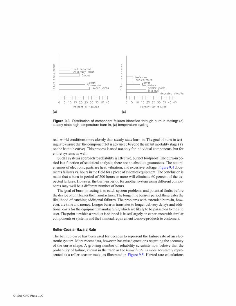
real-world conditions more closely than steady-state burn-in. The goal of burn-in test-ing is to ensure that the component lot is advanced beyond the infant mortality stage (T1on the bathtub curve). This process is used not only for individual components, but forentire systems as well.
Such a systems approach to reliability is effective, but not foolproof. The burn-in pe-riod is a function of statistical analysis; there are no absolute guarantees. The naturalenemies of electronic parts are heat, vibration, and excessive voltage. Figure 9.4 docu-ments failures vs. hours in the field for a piece of avionics equipment. The conclusion ismade that a burn-in period of 200 hours or more will eliminate 60 percent of the ex-pected failures. However, the burn-in period for another system using different compo-nents may well be a different number of hours.
The goal of burn-in testing is to catch system problems and potential faults beforethe device or unit leaves the manufacturer. The longer the burn-in period, the greater thelikelihood of catching additional failures. The problems with extended burn-in, how-ever, are time and money. Longer burn-in translates to longer delivery delays and addi-tional costs for the equipment manufacturer, which are likely to be passed on to the enduser. The point at which a product is shipped is based largely on experience with similarcomponents or systems and the financial requirement to move products to customers.
Roller-Coaster Hazard Rate
The bathtub curve has been used for decades to represent the failure rate of an elec-tronic system. More recent data, however, has raised questions regarding the accuracyof the curve shape. A growing number of reliability scientists now believe that theprobability of failure, known in the trade as the hazard rate, is more accurately repre-sented as a roller-coaster track, as illustrated in Figure 9.5. Hazard rate calculations
Figure 9.3 Distribution of component failures identified through burn-in testing: (a)steady-state high-temperature burn-in, (b) temperature cycling.
(a) (b)
© 1999 CRC Press LLC

require analysis of the number of failures of the system under test, as well as the num-ber of survivors. Advocates of this approach point out that previous estimating pro-cesses and averaging tended to smooth the roller-coaster curve so that the humps wereless pronounced, leading to an incorrect conclusion insofar as the hazard rate wasconcerned. The testing environment also has a significant effect on the shape of thehazard curve, as illustrated in Figure 9.6. Note that at the higher operating tempera-ture (greater environmental stress), the roller-coaster hump has moved to an earlierage.
9.3.2 Environmental Stress Screening
The science of reliability analysis is rooted in the understanding that there is no suchthing as a random failure; every failure has a cause. For reasonably designed and con-structed electronic equipment, failures not caused by outside forces result frombuilt-in flaws or latent defects. Because different flaws are sensitive to differentstresses, a variety of environmental forces must be applied to a unit under test to iden-tify any latent defects. This is the underlying concept behind environmental stressscreening (ESS).
Figure 9.4 The failure history of a piece of avionics equipment vs. time. Note that 60percent of the failures occurred within the first 200 hours of service. (After [1].)
© 1999 CRC Press LLC

ESS, which has come into widespread use for aeronautics and military products,takes the burn-in process a step further by combining two of the major environmentalfactors that cause parts or units to fail: heat and vibration. Qualification testing for
Figure 9.5 The roller-coaster hazard rate curve for electronic systems. (After [2].)
Figure 9.6 The effects of environmental conditions on the roller-coaster hazard ratecurve. (After [2].)
© 1999 CRC Press LLC

products at a factory practicing ESS involves a carefully planned series of checks foreach unit off the assembly line. Units are subjected to random vibration and tempera-ture cycling during production (for subassemblies and discrete components) and uponcompletion (for systems). The goal is to catch product defects at the earliest possiblestage of production. ESS also can lead to product improvements in design and manu-facture if feedback from the qualification stage to the design and manufacturing stagesis implemented. Figure 9.7 illustrates the improvement in reliability that typically canbe achieved through ESS over simple burn-in screening, and through ESS with feed-back to earlier production stages. Significant reductions in equipment failures in thefield can be gained. Table 9.1 compares the merits of conventional reliability testingand ESS.
Designing an ESS procedure for a given product is no easy task. The environmentalstresses imposed on the product must be great enough to cause fallout of marginal com-ponents during qualification testing. The stresses must not be so great, however, as tocause failures in good products. Any unit that is stressed beyond its design limits even-tually will fail. The proper selection of stress parameters—generally, random vibrationon a vibration generator and temperature cycling in an environmental chamber—can,in minutes, uncover product flaws that might take weeks or months to manifest them-selves in the field. The result is greater product reliability for the user.
The ESS concept requires that every product undergo qualification testing beforeintegration into a larger system for shipment to an end user. The flaws uncovered byESS vary from one unit to the next, but types of failures tend to respond to particular en-
Figure 9.7 The effects of environmental stress screening on the reliability bathtubcurve. (After [3].)
© 1999 CRC Press LLC

vironmental stresses. Available data clearly demonstrate that the burn-in screens mustmatch the flaws sought; otherwise, the flaws will probably not be found.
The concept of flaw-stimulus relationships can be presented in Venn diagram form.Figure 9.8 shows a Venn diagram for a hypothetical, but specific, product. The requiredscreen would be different for a different product. For clarity, not all stimuli are shown.Note that there are many latent defects that will not be uncovered by any one stimulus.For example, a solder splash that is just barely clinging to a circuit element probablywould not be broken loose by high-temperature burn-in or voltage cycling, but vibra-tion or thermal cycling probably would break the particle loose. Remember also thatthe defect may be observable only during stimulation and not during a static bench test.
The levels of stress imposed on a product during ESS should be greater than thestress to which the product will be subjected during its operational lifetime, but still bebelow the maximum design parameters. This rule of thumb is pushed to the limits underan enhanced screening process. Enhanced screening places the component or system atwell above the expected field environmental levels. This process has been found to beuseful and cost-effective for many programs and products. Enhanced screening, how-ever, requires the development of screens that are carefully identified during productdesign and development so that the product can survive the qualification tests. En-hanced screening techniques often are required for cost-effective products on a cra-dle-to-grave basis; that is, early design changes for screenability save tremendous costsover the lifetime of the product.
The types of products that can be checked economically through ESS break downinto two categories: high-dollar items and mass-produced items. Units that are physi-cally large in size, such as RF generators, are difficult to test in the finished state. Still,qualification tests using more primitive methods, such as cam-driven truck-bed shak-ers, are practical. Because most large systems generate a large amount of heat, subject-ing the equipment to temperature extremes also may be accomplished. SophisticatedESS for large systems, however, must rely on qualification testing at the subassemblystage.
Table 9.1 Comparison of Conventional Reliability Testing and Environmental StressScreening (After [2].)
Parameter Conventional Testing Environmental StressScreening
Test condition Simulates operational equip-ment profile
Accelerated stress condition
Test sample size Small 100 percent of productionTotal test time Limited HighNumber of failures Small LargeReliability growth Potential for gathering useful
data smallPotential for gathering usefuldata good
© 1999 CRC Press LLC

The basic hardware complement for an ESS test station includes a thermal chambershaker and controller/monitor. A typical test sequence includes 10 minutes of exposureto random vibration, followed by 10 cycles between temperature minimum and maxi-mum. To save time, the two tests may be performed simultaneously.
9.3.3 Latent Defects
The cumulative failure rate observed during the early life of an electronic system isdominated by the latent defect content of the product, not its inherent failure rate.Product design is the major determinant of inherent failure rate. A product design willshow a higher-than-expected inherent rate if the system contains components that aremarginally overstressed, have inadequate functional margin, or contain asubpopulation of components that exhibit a wear-out life shorter than the useful life ofthe product. Industry has grown to expect the high instantaneous failure rate observedwhen a new product is placed into service. The burn-in process, whether ESS or con-ventional, is aimed at shielding customers from the detrimental effects of infant mor-tality. The key to reducing early-product-life failures lies in reducing the number oflatent defects.
A latent defect is some abnormal characteristic of the product or its parts that islikely to result in failure at some point, depending on:
• The degree of abnormality
Figure 9.8 Venn diagram representation of the relationship between flaw precipitationand applied environmental stress. (After [4].)
© 1999 CRC Press LLC

• The magnitude of applied stress
• The duration of applied stress
For example, consider a solder joint on the connecting pin of a vacuum tube device.One characteristic of the joint is the degree to which the pin hole is filled with solder,characterized as “percent fill.” All other characteristics being acceptable, a joint thatis 100 percent filled offers the maximum mechanical strength, minimum resistance,and greatest current carrying capacity. Conversely, a joint that is zero percent filledhas no mechanical strength, and only if the lead is touching the barrel does it have anysignificant electrical properties. Between these two extreme cases are degrees of ab-normality. For a fixed magnitude of applied stress:
• A grossly abnormal solder joint probably will fail in a short time.
• A moderately abnormal solder joint probably will fail, but after a longer period oftime than a grossly abnormal joint.
• A mildly abnormal solder joint probably will fail, but after a much longer periodof time than in either of the preceding conditions.
Figure 9.9 illustrates this concept. A similar time-stress relationship holds for a fixeddegree of abnormality and variable applied stress.
A latent defect eventually will advance to a patent defect when exposed to environ-mental, or other, stimuli. A patent defect is a flaw that has advanced to the point atwhich an abnormality actually exists. To carry on the solder example, a cold solder jointrepresents a flaw (latent defect). After vibration and/or thermal cycling, the joint (it isassumed) will crack. The joint will now have become a detectable (patent) defect. Some
Figure 9.9 Estimation of the probable time to failure from an abnormal solder joint. (Af-ter [5].)
© 1999 CRC Press LLC

latent defects can be stimulated into patent defects by thermal cycling, some by vibra-tion, and some by voltage cycling. Not all flaws respond to all stimuli.
There is strong correlation between the total number of physical and functional de-fects found per unit of product during the manufacturing process, and the average latentdefect content of shipping product. Product- and process-design changes aimed at re-ducing latent defects not only improve the reliability of shipping product, but also resultin substantial manufacturing cost savings.
9.3.4 Operating Environment
The operating environment of an electronic system, either because of external envi-ronmental conditions or unintentional component underrating, may be significantlymore stressful than the system manufacturer or the component supplier anticipated.Unintentional component underrating represents a design fault, but unexpected envi-ronmental conditions are possible for many applications, particularly in remote loca-tions.
Conditions of extreme low or high temperatures, high humidity, and vibration dur-ing transportation may have a significant impact on long-term reliability of the system.For example, it is possible—and more likely, probable—that the vibration stress of thetruck ride to a remote transmitting site will represent the worst-case vibration exposureof the transmitter and all components within it during the lifetime of the product.
Manufacturers report that most of the significant vibration and shock problems forland-based products arise from the shipping and handling environment. Shipping tendsto be an order of magnitude more severe than the operating environment with respect tovibration and shock. Early testing for these problems involved simulation of actualshipping and handling events, such as end-drops, truck trips, side impacts, and rollsover curbs and cobblestones. Although unsophisticated by today’s standards, thesetests are capable of improving product resistance to shipping-induced damage.
9.3.5 Failure Modes
Latent failures aside, the circuit elements most vulnerable to failure in any piece ofelectronic hardware are those exposed to the outside world. In most systems, thegreatest threat typically involves one or more of the following components or subsys-tems:
• The ac-to-dc power supply
• Sensitive signal-input circuitry
• High-power output stages and devices
• Circuitry operating into an unpredictable load, or into a load that may be exposedto lightning and other transient effects (such as an antenna)
Derating of individual components is a key factor in improving the overall reliabilityof a given system. The goal of derating is the reduction of electrical, mechanical, ther-
© 1999 CRC Press LLC

mal, and other environmental stresses on a component to decrease the degradation rateand prolong expected life. Through derating, the margin of safety between the operat-ing stress level and the permissible stress level for a given part is increased. This adjust-ment provides added protection from system overstress, unforeseen during design.
9.3.6 Maintenance Considerations
The reliability and operating costs over the lifetime of an RF system can be affectedsignificantly by the effectiveness of the preventive maintenance program designedand implemented by the engineering staff. In the case of a critical-system unit thatmust be operational continuously or during certain periods, maintenance can have amajor impact—either positive or negative—on downtime.
The reliability of any electronic system may be compromised by an enabling eventphenomenon. This is an event that does not cause a failure by itself, but sets up (or en-ables) a second event that can lead to failure of the system. Such a phenomenon is insid-ious because the enabling event may not be self-revealing. Examples include the fol-lowing:
• A warning system that has failed or has been disabled for maintenance
• One or more controls that are set incorrectly, providing false readouts for opera-tions personnel
• Redundant hardware that is out of service for maintenance
• Remote metering that is out of calibration
Common-Mode Failure
A common-mode failure is one that can lead to the failure of all paths in a redundantconfiguration. In the design of redundant systems, therefore, it is important to iden-tify and eliminate sources of common-mode failures, or to increase their reliability toat least an order of magnitude above the reliability of the redundant system. Com-mon-mode failure points in a high-power RF system include the following:
• Switching circuits that activate standby or redundant hardware
• Sensors that detect a hardware failure
• Indicators that alert personnel to a hardware failure
• Software that is common to all paths in a redundant system
The concept of software reliability in control and monitoring has limited meaning inthat a good program will always run, and copies of a good program will always run. Onthe other hand, a program with one or more errors will always fail, and so will the cop-ies, given the same input data. The reliability of software, unlike hardware, cannot beimproved through redundancy if the software in the parallel path is identical to that inthe primary path.
© 1999 CRC Press LLC

Spare Parts
The spare parts inventory is a key aspect of any successful equipment maintenanceprogram. Having adequate replacement components on hand is important not only tocorrect equipment failures, but to identify those failures as well. Many parts—partic-ularly in the high-voltage power supply and RF chain—are difficult to test understatic conditions. The only reliable way to test the component may be to substitute oneof known quality. If the system returns to normal operation, then the original compo-nent is defective. Substitution is also a valuable tool in troubleshooting intermittentfailures caused by component breakdown under peak power conditions.
9.4 Vacuum Tube ReliabilityThe end user should keep an accurate record of performance for each tube at the facil-ity. Shorter-than-normal tube life could point to a problem in the RF amplifier or re-lated hardware. The average life that may be expected from a power tube is a functionof many operational parameters, including:
• Filament voltage
• Ambient operating temperature
• RF power output
• Operating frequency
• Operating efficiency
The best estimate of life expectancy for a given system at a particular location comesfrom on-site experience. As a general rule of thumb, however, at least 4000 hours ofservice can be expected from most power grid tubes. Klystrons and other microwavedevices typically provide in excess of 15,000 hours. Possible causes of short tube lifeinclude the following:
• Improper power stage tuning
• Inaccurate panel meters or external wattmeter, resulting in more demand from thetube than is actually required
• Poor filament voltage regulation
• Insufficient cooling system airflow
• Improper stage neutralization
An examination of the data sheet for a given vacuum tube will show that a number ofoperating conditions are possible, depending upon the class of service required by theapplication. As long as the maximum ratings of the device are not exceeded, a widechoice of operating parameters is possible. When studying the characteristic curves ofeach tube, remember that they represent the performance of a typical device. All elec-tronic products have some tolerance among devices of a single type. Operation of a
© 1999 CRC Press LLC

given device in a particular system may be different than that specified on the datasheet. This effect is more pronounced at VHF and above.
9.4.1 Thermal Cycling
Most power tube manufacturers recommend a warm-up period between the applica-tion of filament-on and plate-on commands; about 5 minutes is typical. The minimumwarm-up time is 2 minutes. Some RF generators include a time-delay relay to preventthe application of a plate-on command until a predetermined warm-up cycle is com-pleted.
Most manufacturers also specify a recommended cool-down period between the ap-plication of plate-off and filament-off commands. This cool-down, generally about 10minutes, is designed to prevent excessive temperatures on the PA tube surfaces whenthe cooling air is shut off. Large vacuum tubes contain a significant mass of metal,which stores heat effectively. Unless cooling air is maintained at the base of the tubeand through the anode cooling fins, excessive temperature rise can occur. Again, the re-sult can be shortened tube life, or even catastrophic failure because of seal crackscaused by thermal stress.
Most tube manufacturers suggest that cooling air continue to be directed toward thetube base and anode cooling fins after filament voltage has been removed to furthercool the device. Unfortunately, however, not all control circuits are configured to per-mit this mode of operation.
9.4.2 Tube-Changing Procedure
Plug-in power tubes must be seated firmly in their sockets, and the connections to theanodes of the tubes must be tight. Once in place, the device typically requires nomaintenance during its normal operating lifetime.
Insertion of a replacement tube must be performed properly. Gently rock andslightly rotate the tube as it is being inserted into the socket. This will help preventbending and breaking the fingerstock. Be certain to apply sufficient force to seat thetube completely into the socket. Never use a lever or other tool on the tube to set it inplace. Manual pressure should be adequate.
An intermediate point is reached when the grid contact fingerstock slides up thetube sides and encounters the contact area. It is important that the tube is fully insertedin the socket beyond this initial point of resistance.
Some sockets have adjustable stops that are set so that the tube grid contacts rest inthe middle of the contact area when the tube is fully inserted. This positioning can bechecked by inserting, then removing, a new tube. The scratch marks on the grid con-tacts will indicate the position of the tube relative to the socket elements. Figure 9.10shows the minute scoring in the base contact rings of a power grid tube. A well-main-tained socket will score the tube contacts when the device is inserted. If all fingers donot make contact, more current will flow through fewer contact fingers, causing over-heating and burning, as shown in Figure 9.11.
© 1999 CRC Press LLC

Poor contact between a tube and its socket will always lead to problems. If the socketconnectors fail to provide the proper electrical contact with the cylindrical tube ele-ments, concentration of RF charging currents will result, leading to local overheatingthat may be destructive. After the connector loses its spring action, the heating is aggra-vated, and damage to the tube is likely. Some socket designs include a wire-woundspring encircling the outer circumference of the fingerstock to increase the contactpressure of the individual fingers. These springs should be replaced if they break orlose tension.
When a tube is removed from its socket, the socket should be blown or wiped cleanand carefully inspected. Any discoloration caused by overheating of the socketfingerstock could signal impending tube/socket failure.
Figure 9.10 Proper fingerstock scor-ing of filament and control grid con-tacts on a power tube. (Courtesy ofVarian.)
Figure 9.11 Damage to the grid con-tact of a power tube caused by insuffi-cient fingerstock pressure. (Courtesyof Varian.)
© 1999 CRC Press LLC

Many industrial and low-frequency tubes are not socketed, but installed by bolted orclamped connections. Stainless steel has a much lower coefficient of thermal expan-sion than copper. Therefore, clamped stainless steel anode connections should havesome method of strain relief to prevent excess pressure from collapsing the tube anodeas it heats.
All bolted or screwed connections should be tight. Verify that the clamps are snugand provide a good electrical contact around the entire circumference of the device. Be-cause of the RF fields present, all clamps and bolts should be made from nonmagneticmaterials. Copper, brass, and nonmagnetic series 300 stainless steel fasteners are pre-ferred. Stainless steel is not a good conductor of electricity, so, although it may be usedfor clamping, it should not be part of the current path.
Before a new tube is installed in a system, it should be inspected for cracks or looseconnections (in the case of tubes that do not socket-mount). Manufacturers typicallyrecommend that after a new tube—or one that has been on the shelf for some time—isinstalled in the transmitter, it should be run with filaments only for at least 30 minutes,after which plate voltage may be applied. Next, the drive (modulation) is slowlybrought up, in the case of an amplitude-modulated system. Residual gas inside the tubemay cause an interelectrode arc (usually indicated as a plate overload) unless it isburned off in such a warm-up procedure.
9.4.3 Power Tube Conditioning
Large power tubes are subjected to rigorous processing during exhaust pumping at thetime of manufacture [6]. Active elements are processed at temperatures several hun-dred degrees Celsius higher than those expected during normal operation. This proce-dure is designed to drive off surface and subsurface gas from the metals in the deviceto lower the possibility of these gases being released during the service life of thetube. Free gas molecules, however, always will be present to some degree in a fullyprocessed tube. Gas, particularly oxygen-containing compounds, can combine chem-ically with cathode material to either permanently or temporarily destroy the electronemission capability of the cathode. Free gas molecules, when struck by electronsmoving from the cathode to the anode, also may be ionized by having one or moreelectrons knocked from their systems. If enough of these ions, plus freed electrons,are present, a conduction path will be established that is not subject to control by thegrid. This can result in runaway arcing that may involve all elements of the device.Current then will be limited primarily by the source voltage and impedance. (Thespace charge, to some degree, is neutralized by the presence of both electrons andpositive ions.)
Electrons from sources other than the heated cathode provide low-current paths be-tween elements when the voltage gradient is sufficiently high at the negative elementfor pure field emission. The voltage gradient at the negative element is governed by thefollowing parameters:
• The applied voltage between elements
• The spacing between elements
© 1999 CRC Press LLC

• The surface contour of the negative element
A large voltage gradient can exist in the following areas:
• In front of a point on the negative element
• In front of a particle adhering to the negative element
• In front of a clump of gas molecules on the surface of the negative element
Field emission occurs readily from a cold surface if the operating conditions providethe necessary voltage gradient.
Ionization of free gas can result from bombardment by field-emitted electrons.Arcing is likely to occur as a result of field emission in operating equipment becausethe plate voltage is maximum during that part of the signal cycle when ordinary platecurrent from the cathode is shut off by the control grid. For this reason, an importantpart of tube processing is high-voltage conditioning to remove sharp points or smallparticles from tube elements. This part of tube processing may, and sometimes should,be repeated in the field after shipment or storage if the tube is intended for use at a platevoltage in excess of 10 kV.
High-voltage conditioning (sometimes called spot-knocking or debarnacling) con-sists of applying successively higher voltages between tube elements, permitting thetube to spark internally at each voltage level until stable (no arcing). The voltage then israised to the next higher potential until the tube is stable at a voltage approximately 15percent higher than the peak signal voltage it will encounter in service.
The equipment used for tube conditioning is simple but specialized. It may providedc or ac voltage, or both. The current required is small. The voltage should be continu-ously variable from practically zero to the highest value required for proper condition-ing of the tube. The energy per spark is controlled by the internal resistance of the sup-ply plus any external series resistor used. In dc conditioning, a milliammeter typicallyis included to measure the level of field emission current prior to sparking, or simply todetermine whether the field emission current is within the specified range for a tube be-ing tested. Also in dc conditioning, a capacitor may be placed across the tube under testto closely control the energy released for each spark. If the conditioning is to proceedeffectively, the amount of energy delivered by the capacitor must be great enough tocondition the surfaces, but not so large as to cause permanent damage.
Power Supply
The power supply is the heart of any high-voltage tube conditioning station [6]. Cur-rent-limiting resistance is desirable; the power supply may have an internal resistanceon the order of 100 kΩ. In addition to the power supply, a current-limiting resistor of100 to 300 kΩ should be provided in the circuit to the tube being conditioned. In dcprocessing, a storage capacitor of 1000 to 3000 pF can be placed directly across thedevice under test (DUT), with a high-voltage noninductive resistor of approximately50 Ω connected between the tube and the capacitor. Naturally, this shunt capacitormust be capable of withstanding the full applied potential of the power supply.
© 1999 CRC Press LLC
Using both polarities on the tube elements is advantageous in high-voltage condi-tioning, suggesting that an ac supply might be the best choice for field tube condition-ing. The advantage of the dc system, on the other hand, is that exact levels of field emis-sion current and breakdown voltage may be determined for comparison with known“clean” tubes, and with the manufacturer’s specification. The polarity of the appliedvoltage may be reversed by mounting the DUT on an insulating frame so that the posi-tive and negative high-voltage leads may be interchanged during processing. Also, thepower supply rectifier and dc meters may be bypassed with suitable switching so that acis obtained from the supply for initial tube cleanup. The storage capacitor across thetube should be disconnected if ac is used.
Conditioning Procedure
Manufacturers of large power tubes typically specify an upper limit for field emissionbetween the filament, control grid, and screen grid connected together, and the anode[6]. Such devices should be allowed to spark until stable at the voltage where sparkingfirst occurs. The voltage then is increased in steps determined by the voltage that initi-ates sparking again. This process is continued until the tube is stable at the maximumtest voltage. It is advisable to reverse the polarity of the supply if dc testing is em-ployed.
Usually, no field emission specifications exist for applied voltage between grids andbetween grid and filament, but these elements normally should hold off 10 kV inter-nally. The need for conditioning between these elements is indicated if internal spark-ing occurs at a significantly lower voltage. Consult the tube manufacturer for specificrecommendations on conditioning voltages.
During high-voltage processing, particularly between grids and between grid andfilament, some of the redistributed gas molecules may be deposited on the cold fila-ment, causing a temporary loss of emission. If this happens, operate the tube for ap-proximately 1 hour, with normal filament power only, to drive off the volatile material.Normal electron emission from the filament will be reestablished by this procedure. Itis recommended that routine practice include operation of the filament for approxi-mately 1 hour as an immediate follow-up to high-voltage conditioning.
After conditioning, the tube should be stored in the same position (orientation) asthat used for high-voltage conditioning and installation in the equipment. Movement ofthe tube after conditioning should be minimized to prevent any redistribution of parti-cles within the device.
Considerations for Very Large Tubes
High-voltage ac conditioning is not recommended for very large tubes, such as the8971/X2177, 8972/X2176, 8973/X2170, 8974/2159, 4CM400000A, and similar de-vices [6]. High-potential 50 or 60 Hz voltage can excite natural mechanical reso-nances in the large filament and grid structures of these tube types. Excitation of theseresonances can break the filament and/or grids, thus destroying the device. If ac con-ditioning must be used, the following precautions should be taken:
© 1999 CRC Press LLC
• Connect all filament terminals together (external to the tube).
• Connect all terminals of the tube to a terminal of the high-voltage power supply.For example, if high voltage is to be applied between the screen and anode, the fil-ament, grid, and screen should be connected together, then to one terminal of thesupply. If high voltage is to be applied between the filament and grid, connect thegrid, screen, and anode together and to one terminal of the supply. No terminal ofthe tube should be allowed to float electrically during high-voltage conditioning.
• As the test voltage is increased, listen carefully for vibration inside the tube. Ifany is detected, immediately remove the ac high voltage.
These precautions will reduce the risk of damage from ac conditioning of very largetubes. However, because of the special procedures required and the risk of damage re-sulting from mechanical resonances, it is recommended that only dc conditioning beused for such devices.
Safety
Personnel protection dictates that the tube being processed, as well as the power sup-ply, be enclosed in a metal cabinet with access doors interlocked so that no high volt-age can be applied until the doors are closed [6]. The enclosure material, wall thick-ness, and dimensions must be chosen to limit X-ray radiation from the DUT to safelevels. A steel-wall thickness of in has been found adequate for dc testing up to ap-proximately 70 kV. For conditioning up to 100 kV dc, it is necessary to add 0.05 in oflead sheet as a lining to the steel enclosure.
The field of health standards regarding x-radiation dosage for a given period of timeis complex and should be discussed with experts on the subject. Calibrated film badgesor other reliable measuring devices normally are used to determine human exposure toX rays over time.
9.4.4 Filament Voltage
A true reading rms voltmeter is required for accurate measurement of filament volt-age. The measurement is taken directly from the tube socket connections. Atrue-reading rms meter, instead of the more common average responding rms meter,is suggested because it can accurately measure a voltage despite an input waveformthat is not a pure sine wave. Some filament voltage regulators use silicon controlledrectifiers (SCRs) to regulate the output voltage. Saturated core transformers, whichoften deliver nonsine waveforms, also are commonly used to regulate filament inputpower.
Long tube life requires filament voltage regulation. A tube whose filament voltageis allowed to vary along with the primary line voltage will not achieve the life expec-tancy possible with a tightly regulated supply. This problem is particularly acute atmountain-top installations, where utility regulation is generally poor.
To extend tube life, some end-users leave the filaments on at all times, not shuttingdown at sign-off. If the sign-off period is 3 hours or less, this practice can be beneficial.
© 1999 CRC Press LLC

Filament voltage regulation is a must in such situations because the primary line volt-ages may vary substantially from the carrier-on to carrier-off value.
When a cold filament is turned-on, damage can be caused by two effects [7]:
• Current inrush into the cold filament, which can be up to 10 times the normal op-erating current if the filament supply is of low impedance.
• Grain reorientation, which occurs at about 600 to 700 ºC, known as theMiller-Larson effect. This grain reorientation will result in a momentary plasticstate that can cause the filament wire to grow in length and, therefore, becomethinner.
The Miller-Larson effect is aggravated by variations in the cross-sectional area of thefilament wires along their length. This will cause hot spots in the thinner sections be-cause of the greater current densities there. The higher temperatures at the hot spotscause increased growth during warmup through the 600 ºC temperature range, whenthey have a higher current density than the rest of the wire, and a much higher powerdissipation per unit length as a result of the higher resistance. Each time the filamentis turned-on, the wire becomes thinner until the hot spot temperature enters a runawaycondition.
Filament voltage for a klystron should not be left on for a period of more than 2 hoursif no beam voltage is applied. The net rate of evaporation of emissive material from thecathode surface of a klystron is greater without beam voltage. Subsequent condensa-tion of the material on gun components may lead to voltage holdoff problems and an in-crease in body current.
Black Heat
One practice used occasionally to extend the life of the thoriated tungsten power tubefilament is to operate the device at a low percentage of rated voltage during sign-offperiods [7]. This technique, known as black heat, involves operating the filament at25 to 40 percent of the rated filament voltage. This range produces a temperature highenough to maintain the filament above the 600 ºC region where the Miller-Larson ef-fect occurs, and sometimes low enough so that forced cooling is not required duringstand-by.
Operating histories of several black heat installations indicate that the trauma ofraising the filament voltage from 25 percent up to the operating voltage is still poten-tially damaging. For this reason, a higher stand-by voltage of about 80 to 90 percent ofthe full rated value (orange heat) has been used with some success.
The voltage range of 40 to 80 percent should be avoided because the filament can actas a getter within this range, and absorb gases that will raise the work function of thethoriated tungsten filament. For orange heat operation, cooling system operation is re-quired. Before attempting to implement a black heat or orange heat filament manage-ment program, consult with the tube and transmitter manufacturers.
© 1999 CRC Press LLC

9.4.5 Filament Voltage Management
As outlined in Chapter 3, the thoriated-tungsten power grid tube lends itself to life ex-tension through management of the applied filament voltage. Accurate adjustment ofthe filament voltage can extend the useful life of the device considerably, sometimesto twice the normal life expectancy. The following procedure typically is recom-mended:
• Install the tube, and tune for proper operation.
• Operate the filament at its full rated voltage for the first 200 hours following in-stallation.
• Following the burn-in period, reduce the filament voltage by 0.1 V per step untilsystem power output begins to fall (for frequency-modulated systems) or untilmodulating waveform distortion begins to increase (for amplitude-modulatedsystems).
• When the emissions floor has been reached, increase the filament voltage approx-imately 0.2 V peak-to-peak (P-P).
Long-term operation at this voltage can result in a substantial extension of the usefullife of the tube, as illustrated in Figure 9.12.
The filament voltage should not, in any event, be operated at or below 90 percent ofits rated value. At regular intervals, about every 3 months, the filament voltage ischecked and increased if power output begins to fall or waveform distortion begins torise. Filament voltage never should be increased to more than 105 percent of the ratedvoltage.
Note that some tube manufacturers place the minimum operating point at 94 per-cent. Others recommend that the tube be set for 100 percent filament voltage and leftthere. The choice is left to the user, after consultation with the manufacturer.
The filament current should be checked when the tube is installed, and at annual in-tervals thereafter, to ensure that the filament draws the expected current. Tubes can failearly in life because of an open filament bar—a problem that could be discovered dur-ing the warranty period if a current check is made upon installation.
For 1 week of each year of tube operation, the filament should be run at full ratedvoltage. This will operate the getter and clean the tube of gas.
Klystron Devices
Filament voltage is an equally important factor in achieving long life in a klystron.The voltage recommended by the manufacturer must be accurately set and checkedon a regular basis. Attempts have been made to implement a filament voltage man-agement program—as outlined previously for a thoriated-tungsten tube—on a kly-stron, with varying degrees of success. If filament management is attempted, the fol-lowing guidelines should be observed:
© 1999 CRC Press LLC

Figure 9.12 The effects of filament voltage management on a thoriated-tungsten fila-ment power tube: (a) useful life as a function of filament voltage, (b) available power as afunction of filament voltage. Note the dramatic increase in emission hours when filamentvoltage management is practiced.
(b)
(a)
© 1999 CRC Press LLC

• Install the tube, and tune for proper operation.
• Operate the filament at its full rated voltage for the first 200 hours following in-stallation.
• Following the burn-in period, reduce the filament voltage by 0.1 V per step untilcollector current begins to decrease. After each filament voltage change, wait atleast 5 minutes to allow for cathode cooling.
• When the emissions floor has been reached, increase the filament voltage approx-imately 0.25 V P-P.
Figure 9.13 charts the relationship between emitter temperature and beam current.The filament should be adjusted to a point between Ef1 and Ef2, which will vary witheach klystron. Note that continued operation below the Ef1 level, or at a point thatcauses emission instability, can result in beam defocusing, leading to increased modu-lating anode current and body current.
For operation at a reduced filament voltage, it may be necessary to allow a longerwarm-up period when bringing the tube up from a cold start. If loss of emission is notedat turn-on, it will be necessary to either extend the warm-up time or raise the filamentvoltage to overcome the loss.
9.4.6 PA Stage Tuning
The PA stage of an RF generator may be tuned in several ways. Experience is the bestteacher when it comes to adjusting for peak efficiency and performance. Compro-mises often must be made among various operating parameters.
Figure 9.13 The effect of klystron emitter temperature on beam current.
© 1999 CRC Press LLC

Tuning can be affected by any number of changes in the PA stage. Replacing the fi-nal tube in a low- to medium-frequency RF generator usually does not significantly al-ter stage tuning. It is advisable, however, to run through a touch-up tuning procedurejust to be sure. Replacing a tube in a high-frequency RF generator, on the other hand,can significantly alter stage tuning. At high frequencies, normal tolerances and varia-tions in tube construction result in changes in element capacitance and inductance.Likewise, replacing a component in the PA stage may cause tuning changes because ofnormal device tolerances.
Stability is one of the primary objectives of tuning. Adjust for broad peaks or dips, asrequired. Tune so that the system is stable from a cold startup to normal operating tem-perature. Readings should not vary measurably after the first minute of operation.
Tuning is adjusted not only for peak efficiency, but also for peak performance.These two elements, unfortunately, do not always coincide. Tradeoffs must sometimesbe made to ensure proper operation of the system.
9.4.7 Fault Protection
An arc is a self-sustained discharge of electricity between electrodes with a voltagedrop at the cathode on the order of the minimum ionizing potential of the environment[8]. The arc supports large currents by providing its own mechanism of electron emis-sion from the negative terminal, plus space-charge neutralization.
All power vacuum tubes operate at voltages that can cause severe damage in theevent of an internal arc unless the tube is properly protected. This damage can be rela-tively minor in tubes operating from low-energy power supplies, but it will become cat-astrophic in cases where a large amount of stored energy or follow-on current is in-volved. Because any high-voltage vacuum device may arc at one time or another, somemeans of protection is advised in all cases; it is mandatory in those instances where de-structive quantities of energy are involved. In addition to protecting the tube in theevent of a tube or circuit malfunction, such measures also protect the external circuitry.
Most power grid tubes employing thoriated-tungsten filaments are capable of with-standing relatively high energy arcs. However, while employing substantial materials,such devices usually incorporate fine wire grids that must be protected. In large tubeapplications, it is often found that the screen grid or bias supply, in addition to the anodesupply, is capable of delivering destructive energy to the tube structure in the event of aninternal arc. Consequently, protection must be provided in all cases where potentiallydestructive energy is involved. Large tubes usually are capable of withstanding up to 50joules (J) total energy without permanent damage.
In the design of a power amplifier, the stage should be tested to ensure that the 50 Jlimit is not exceeded by any of the power supplies feeding the tube. Each supply,whether anode or grid, should be short-circuit-tested through a 6-in length of0.255-mm-diameter (no. 30 AWG) soft copper wire. A similar test should be madefrom plate-to-screen grid to ensure that the tube is protected in the event of aplate-to-screen arc. A protective spark gap between the screen grid and cathode is rec-ommended so that, if an arc occurs, the resulting spark from screen to cathode is exter-nal to the tube structure. The test wire will remain intact if the energy dissipated is less
© 1999 CRC Press LLC

than 50 J. The 50 J test includes total energy delivered from the energy storage deviceand/or from the follow-on current from the power supply prior to the opening of the pri-mary circuit.
Each power supply in the system must pass this test, or some form of energy-divert-ing or energy-limiting circuit must be employed. Figure 9.14 shows an energy-divert-ing circuit for a high-power tube. Energy diverters at high-power levels are complex.They typically employ large high-speed diverting elements such as thyratrons,ignitrons, triggered spark gaps, and, in some cases, a high-speed vacuum switch. Thesedevices may be required to handle thousands of amperes of peak current. Resistor R1 inFigure 9.14 is used to limit the peak current into the energy-diverting switch V1, as wellas to limit peak current demand on the transformer and rectifiers in the power supply.Resistor R2 must be large enough to keep the voltage across V1 from dropping so lowunder load-arc conditions as to inhibit the proper firing of the fault-diverting elements.R1 and R2 must also damp circuit ringing sufficiently to prevent current reversal in V1,which could cause V1 to open before the fault conditions are cleared. R1 and R2 aresized to minimize average power losses and to handle the required voltage and powertransients while properly performing their functions. The sensing element CT1 detectsany abnormal peak-current levels in the system. Signals from the current transformerare used to trigger V1 in the event of an overcurrent condition. A crowbar test switch,S1, can be used to perform the wire test outlined previously, to ensure that the total en-ergy dissipated in an arc is less than 50 J. Typically, S1 is a remote-controlled high-volt-age switch of either air or vacuum construction.
In a typical test, when S1 is closed, current transformer CT1 senses the fast risingcurrent and fires the energy-diverting element V1; it simultaneously sends a fast tripsignal to the main circuit breaker. Most energy diverters fire within a few microsecondsof the time the fault is detected; all voltages and currents are removed from the pro-tected device in tens of microseconds.
Figure 9.14 Arc protection circuit utilizing an energy-diverting element.
© 1999 CRC Press LLC

By using this technique, it is possible to limit the energy delivered during an arc tomuch less than the recommended maximum. In a properly operating system, essen-tially no damage will occur within the tube even under severe arcing conditions. Thetest wire must be connected at the tube itself to take into account all stored energy (Land C) in the system.
9.4.8 Vacuum Tube Life
The vacuum tube suffers wear-out because of a predictable chemical reaction. Lifeexpectancy is one of the most important factors to be considered in the use of vacuumtubes. In general, manufacturers specify maximum operating parameters for powergrid tubes so that operation within the ratings will provide for a minimum useful lifeof 4000 hours. Considerable variation can be found with microwave power tubes, but15,000 hours is probably a fair average useful life. It should be noted that some micro-wave devices, such as certain klystrons, have an expected useful life of 30,000 hoursor more.
The cathode is the heart of a power tube. The device is said to wear out when fila-ment emissions are inadequate for full power output or acceptable waveform distortion.In the case of the common thoriated-tungsten filament tube, three primary factors de-termine the number of hours a device will operate before reaching wear-out:
• The rate of evaporation of thorium from the cathode
• The quality of the tube vacuum
• The operating temperature of the filament
In the preparation of thoriated tungsten, 1 to 2 percent of thorium oxide (thoria) isadded to the tungsten powder before it is sintered and drawn into wire form. After beingmounted in the tube, the filament usually is carburized by being heated to a tempera-ture of about 2000 K in a low-pressure atmosphere of hydrocarbon gas or vapor until itsresistance increases by 10 to 25 percent. This process allows the reduction of the thoriato metallic thorium. The life of the filament as an emitter is increased because the rateof evaporation of thorium from the carburized surface is several times smaller thanfrom a surface of pure tungsten.
Despite the improved performance obtained by carburization of a thoriated-tung-sten filament, the element is susceptible to deactivation by the action of positive ions.Although the deactivation process is negligible for anode voltages below a criticalvalue, a trace of residual gas pressure too small to affect the emission from a pure tung-sten filament can cause rapid deactivation of a thoriated-tungsten filament. This re-striction places stringent requirements on vacuum processing of the tube.
These factors, taken together, determine the wear-out rate of the device. Cata-strophic failures due to interelectrode short circuits or failure of the vacuum envelopeare considered abnormal and are usually the result of some external influence. Cata-strophic failures not the result of the operating environment usually are caused by a de-fect in the manufacturing process. Such failures generally occur early in the life of thecomponent.
© 1999 CRC Press LLC

The design of the RF equipment can have a substantial impact on the life expectancyof a vacuum tube. Protection circuitry must remove applied voltages rapidly to preventdamage to the tube in the event of a failure external to the device. The filament turn-oncircuit also can affect PA tube life expectancy. The surge current of the filament circuitmust be maintained below a certain level to prevent thermal cycling problems. Thisconsideration is particularly important in medium- and high-power PA tubes. When theheater voltage is applied to a cage-type cathode, the tungsten wires expand immedi-ately because of their low thermal inertia. However, the cathode support, which is madeof massive parts (relative to the tungsten wires), expands more slowly. The resultingdifferential expansion can cause permanent damage to the cathode wires. It also cancause a modification of the tube operating characteristics and, occasionally, arcs be-tween the cathode and the control grid.
Catastrophic Failures
Catastrophic failures can be divided into two primary categories:
• The short-circuiting of broken or warped elements within the tube
• A loss of vacuum in the device
Air in the tube causes a loss of dielectric standoff between the internal elements. It isnot possible to distinguish between an interelectrode short circuit and a loss of vac-uum in the operating equipment.
Catastrophic failures that occur during initial installation are usually the result ofbroken elements. Failures that occur after an initial burn-in period are more likely to becaused by a loss of vacuum. In either case, continued efforts to operate the tube can re-sult in considerable damage to the device and to other components in the system.
Note that a loss of vacuum can result from any of several anomalies. The two mostcommon are:
• A latent manufacturing defect in one of the ceramic-to-metal seals
• Circulating currents resulting from parasitic oscillations and/or improper tuning
Intermittent overloads are the most difficult to identify. They can be caused by cir-cuit operating conditions or internal tube failures. A broken or warped filament ele-ment, for example, can move around inside the device and occasionally short circuit tothe grid, causing a loss of grid bias and subsequent plate overload. Intermittent over-loads also can be caused by a short circuit or high VSWR across the load.
9.4.9 Examining Tube Performance
Examination of a power tube after it has been removed from a transmitter or othertype of RF generator can reveal a great deal about how well the equipment-tube com-bination is working. Contrast the appearance of a new power tube, shown in Figure9.15, with a component at the end of its useful life. If a power tube fails prematurely,
© 1999 CRC Press LLC

the device should be examined to determine whether an abnormal operating conditionexists within the transmitter. Consider the following examples:
• Figure 9.16. Two 4CX15000A power tubes with differing anode heat-dissipationpatterns. Tube (a) experienced excessive heating because of a lack of PA com-partment cooling air or excessive dissipation because of poor tuning. Tube (b)shows a normal thermal pattern for a silver-plated 4CX15000A. Nickel-platedtubes do not show signs of heating because of the high heat resistance of nickel.
• Figure 9.17. Base-heating patterns on two 4CX15000A tubes. Tube (a) shows ev-idence of excessive heating because of high filament voltage or lack of cooling airdirected toward the base of the device. Tube (b) shows a typical heating patternwith normal filament voltage.
• Figure 9.18. A 4CX5000A tube with burning on the screen-to-anode ceramic.Exterior arcing of this type generally indicates a socketing problem, or anothercondition external to the tube.
• Figure 9.19. The stem portion of a 4CX15000A tube that had gone down to airwhile the filament was on. Note the deposits of tungsten oxide formed when thefilament burned up. The grids are burned and melted because of the ionizationarcs that subsequently occurred. A failure of this type will trip overload breakersin the RF generator. It is indistinguishable from a short-circuited tube in opera-tion.
• Figure 9.20. A 4CX15000A tube that experienced arcing typical of a bentfingerstock, or exterior arcing caused by components other than the tube.
Figure 9.15 A new, unused4CX15000A tube. Contrast the ap-pearance of this device with the tubesshown in the following figures. (Cour-tesy of Varian.)
© 1999 CRC Press LLC

Figure 9.16 Anode dissipation patterns on two 4CX15000A tubes: (a) excessive heat-ing, (b) normal wear. (Courtesy of Econco Broadcast Service.)
(a) (b)
Figure 9.17 Base heating patterns on two 4CX15000A tubes: (a) excessive heating, (b)normal wear. (Courtesy of Econco.)
(a) (b)
© 1999 CRC Press LLC

Note that the previous examples apply to silver-plated power grid tubes.The external metal elements of a tube typically are plated with nickel or silver. Tubes
that go into sockets are usually silver-plated. The soft silver provides a better contact in-terface than the much harder nickel, and it deforms slightly under contact pressure, pro-viding greater contact area. Silver plating has a dull, whitish cast, whereas nickel has ahard, metallic appearance.
Nickel is resistant to discoloration due to heat at normal tube operating tempera-tures, but silver will tarnish easily. As demonstrated in this section, the heat patterns on
Figure 9.18 A 4CX5000A tube that appears tohave suffered socketing problems. (Courtesy ofEconco.)
Figure 9.19 The interior elements of a4CX15000A tube that had gone to air while the fila-ment was lit. (Courtesy of Econco.)
© 1999 CRC Press LLC
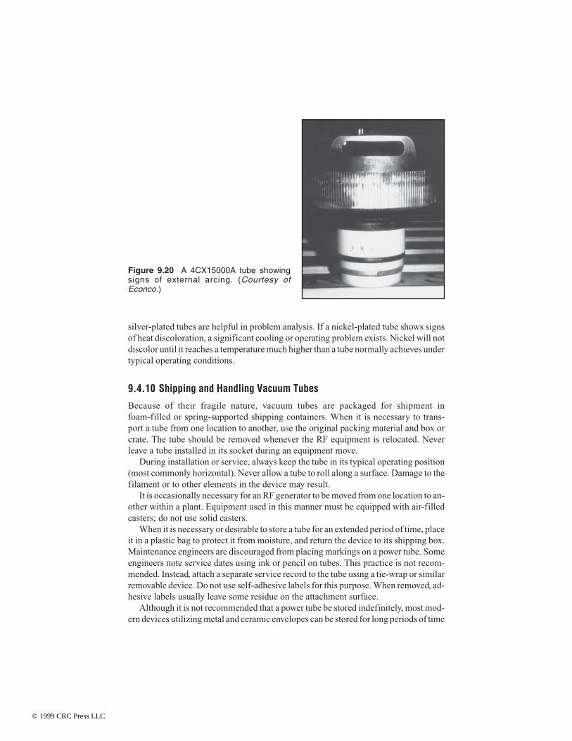
silver-plated tubes are helpful in problem analysis. If a nickel-plated tube shows signsof heat discoloration, a significant cooling or operating problem exists. Nickel will notdiscolor until it reaches a temperature much higher than a tube normally achieves undertypical operating conditions.
9.4.10 Shipping and Handling Vacuum Tubes
Because of their fragile nature, vacuum tubes are packaged for shipment infoam-filled or spring-supported shipping containers. When it is necessary to trans-port a tube from one location to another, use the original packing material and box orcrate. The tube should be removed whenever the RF equipment is relocated. Neverleave a tube installed in its socket during an equipment move.
During installation or service, always keep the tube in its typical operating position(most commonly horizontal). Never allow a tube to roll along a surface. Damage to thefilament or to other elements in the device may result.
It is occasionally necessary for an RF generator to be moved from one location to an-other within a plant. Equipment used in this manner must be equipped with air-filledcasters; do not use solid casters.
When it is necessary or desirable to store a tube for an extended period of time, placeit in a plastic bag to protect it from moisture, and return the device to its shipping box.Maintenance engineers are discouraged from placing markings on a power tube. Someengineers note service dates using ink or pencil on tubes. This practice is not recom-mended. Instead, attach a separate service record to the tube using a tie-wrap or similarremovable device. Do not use self-adhesive labels for this purpose. When removed, ad-hesive labels usually leave some residue on the attachment surface.
Although it is not recommended that a power tube be stored indefinitely, most mod-ern devices utilizing metal and ceramic envelopes can be stored for long periods of time
Figure 9.20 A 4CX15000A tube showingsigns of external arcing. (Courtesy ofEconco.)
© 1999 CRC Press LLC

without deterioration. It usually is not necessary to rotate a spare tube through an oper-ating socket to degas the device.
Older vacuum tubes utilizing glass as the insulating medium tend to leak gas overtime. The glass is not the problem, but, instead, the Kovar alloy used to seal theglass-to-metal parts of the tube. Kovar also is subject to rusting when moisture is pres-ent. Glass-insulated vacuum tubes should be sealed in a plastic bag for storage and ro-tated through the equipment at least once every 12 months. The larger the physical sizeof the tube, the greater the problem of gassing.
9.5 Klystron ReliabilityKlystron amplifiers are well known as reliable, long-life microwave devices that pro-vide the user thousands of hours of trouble-free service. Many of the guidelines dis-cussed in Section 9.4 for power vacuum tubes in general also apply to klystrons andrelated microwave devices. However, several considerations are specific to the kly-stron, including:
• Cooling system maintenance
• Ceramic element cleanings
• Gun element reconditioning
• Focusing electromagnet maintenance
• Protection during prime power interruption
• Shutoff precautions
9.5.1 Cleaning and Flushing the Cooling System
One of the major problems encountered in field operation of a klystron cooling sys-tem is the formation of corrosion products [9]. Corrosion frequently occurs in thecooling channels of the klystron body on the surface of the water/vapor-cooled collec-tor, and in the cooling channels of the electromagnet. It is the result of a chemical re-action between free oxygen-laden coolant and the hot copper channel wall. Corro-sion, as described here, is different from scale formation, which can be caused by theuse of a coolant other than clean distilled water, or may be the by-product of electroly-sis between dissimilar metals in the heat-exchange system. Scale formation can becontrolled through the use of on-line purification loops.
New transmitter water lines frequently contain contaminants, including:
• Solder
• Soldering or brazing flux
• Oils
• Metal chips or burrs
© 1999 CRC Press LLC

• Pieces of Teflon sealing tape
When the water lines are installed, these contaminants must be flushed and cleanedfrom the system before the klystron and magnet are connected.
The following guidelines are suggested for cleaning the cooling passages of water-and vapor-cooled klystrons and associated RF generation equipment. The proceduresshould be performed before a klystron is installed, then repeated on a periodic basiswhile the tube is in service.
Transmitter Flushing
Proper cleaning of the circulating water system in an RF generator is vital tolong-term reliability. Although each design is unique, the following general proce-dures are appropriate for most installations [9]:
• Disconnect the tube and the magnet.
• Add jumper hoses between the input and output of the klystron and the electro-magnet water lines.
• Disconnect or bypass the pump motor.
• Fill the system with hot tap water, if available.
• Open the drain in the transmitter cabinet and flush for 15 minutes or until it isclean.
• Flush the water lines between the tank and pump separately with hot tap water, ifavailable, until they are clean.
• Connect all water lines, and fill the system with hot tap water, if available, andone cup of nonsudsing detergent. Trisodium phosphate is recommended.
• Operate the water system with hot tap water for 30 minutes. An immersion heatermay be used to maintain hot water in the system.
• Drain the system, and flush with hot tap water for 30 minutes.
• Remove and clean the filter element.
• Refill the water system with tap water (at ambient temperature).
• Operate the water system. Maintain the water level while draining and flushingthe system until no detergent, foam, or foreign objects or particles are visible inthe drained or filtered element. To test for detergents in the water, drain a sampleof water into a small glass test tube, and allow it to stand for 5 minutes. To gener-ate foam, shake the test tube vigorously for 15 s, then allow it to stand 15 s. Acompletely foam-free surface indicates no foam-producing impurities.
• Repeat the two previous steps if detergent foam is still present.
• Drain the system and refill with distilled water when the tube and transmitter wa-ter lines are clean.
© 1999 CRC Press LLC

• Remove, clean, and replace the filter before using.
Flushing Klystron Water Lines
Although most klystrons are shipped from the manufacturer with water passagesclean and dry, it is good engineering practice to flush all cooling passages before in-stalling the tube. Occasionally, tubes that have been in service for some time developscale on the collector and also must be flushed. Contaminated water further contrib-utes to dirty water lines, requiring flushing to clear. The following general procedureis recommended for tubes with contaminated water lines, corrosion, scale, or blockedpassages [9]:
• Remove the input water fitting (Hansen type), and add a straight pipe extension,approximately 1 to 2 in long, to the tube.
• Attach a hose to this fitting, using a hose clamp to secure it. This connection willserve as the drain line; it should be discharged into a convenient outlet.
• On some tube types, the normal body-cooling output line is fed to the base of thevapor-phase boiler. Remove the hose at the base of the boiler. Do not damage thisfitting; it must be reused and must seal tightly.
• Attach a 2 to 3 in-long extension pipe that will fit the small hose at one end and agarden hose at the other end. Secure the extension with hose clamps.
• Connect the garden hose to a tap water faucet. Hot tap water is preferable, if avail-able.
• Back-flush the klystron-body cooling passages for 10 to 15 minutes at full pres-sure until they are clean.
• Reconnect the input and output water lines to the klystron.
• If scale is present on the vapor-phase collector, use a solution of trisodium phos-phate for the first cleaning. Perform this step after cleaning the transmitter watersystem (as described previously).
• Connect the klystron to the transmitter water lines, and fill the system with tapwater (hot, if available) and one cup of nonsudsing detergent.
• Operate the water system for 15 minutes. Make certain that the water level com-pletely covers the collector core.
• Drain the system, and flush for 30 minutes or until no detergent foam is present.
• Remove and clean the filter element.
• Fill the system with distilled water.
• Drain the system, and refill with distilled water.
© 1999 CRC Press LLC

Cleaning Klystron Water Lines
If heavy scaling has formed on the vapor-phase collector and/or blocked water pas-sages, they may be cleaned using a stronger cleaning agent. A solution of Ty-Sol1 maybe used to remove scale and corrosion. The following procedure is recommended [9]:
• Clean the transmitter water system (as described previously).
• Connect the tube to the transmitter water system.
• Fill the system with hot tap water (if available) and add 2 gallons of cleaning solu-tion for every 50 gallons of water.
• Operate the water system for 15 minutes, or until scale has been removed and thecollector has a clean copper color.
• Make certain that the water level covers the top of the collector during cleaning.Evidence of cleaning action may be observed in the flow meters.
• Drain the system, and flush with tap water.
• Remove and clean the filter element, then replace.
• Refill the system with distilled water and flush for 30 minutes to 1 hour.
• Check for detergent foam at the end of the flushing period; also check the pH fac-tor. Continue flushing with distilled water if foam is present or if the pH factor isnot within the specified range.
• Refill the system with clean distilled water.
Chlorine present in common tap water is harmful to the water passages of the kly-stron. Thorough flushing with distilled water will remove all chlorine traces. Neveruse tap water for final refill or for make-up water.
Flushing and Cleaning Magnet Water Lines
The magnet water lines may be flushed and cleaned in the same manner as describedfor the klystron.
General Cleaning
Two remaining items must be clean to achieve efficient operation: the sight glass andfloat of the water-flow indicators. The water-flow indicators often become contami-nated during use. This contamination collects on the sight glass and on the float, mak-ing flow-reading difficult. If too much contamination is present on the glass and float,sticking or erroneous readings may result. The detergent and cleaning solutions may
1 Chemical Research Association, Chicago, IL.
© 1999 CRC Press LLC

not remove all of this contamination. If this is the case, remove and clean the flow me-ter using a brush to clean the glass surface.
9.5.2 Cleaning Ceramic Elements
Foreign deposits on the ceramic elements of a klystron should be removed periodi-cally to prevent ceramic heating or arc paths that can lead to klystron failure. The rec-ommended procedure is as follows:
• Remove the klystron from the RF generator, and mount it to a stand or other suit-able fixture.
• Remove loose debris with a soft-fiber bristle brush.
• Clean the ceramic with a mild abrasive cleanser, preferably one that includes ableaching agent. (Household cleansers such as Comet and Ajax are acceptable.)While cleaning, do not apply excessive force to the ceramic. Normal hand pres-sure is sufficient.
• Flush the ceramic with clean water to remove the cleanser.
• Flush a second time with clean isopropyl alcohol.
• Air dry the device. Be certain that all moisture has evaporated from the tube be-fore returning it to service.
9.5.3 Reconditioning Klystron Gun Elements
During the operational life of a klystron, voltage standoff problems may be experi-enced when the operating mode of the device is changed from one collector voltage toa higher voltage, or from continuous to pulsed service [10]. In both of these cases, thedifference of potential between the internal elements is increased over values used inthe previous mode of operation. In some instances, this elevated difference of poten-tial can lead to internal arcing as a result of long-term buildup of electrical leakagebetween elements. This is a part of the normal aging process in klystrons. In manycases, however, this particular process can be reversed through high-voltage condi-tioning. Maintenance engineers have found it useful to clear any residual leakage be-tween the various elements before pulsing an older klystron, or when increasing theoperating potentials applied to an older klystron.
Klystron electron gun leakage can be checked, and, in many cases, the gun elementsreconditioned, by applying a high dc potential between these elements. The process istermed hi-potting. It requires a current-limited (5 mA maximum), continuously-vari-able dc supply with a range of 0 to 30 kV. The procedure is as follows:
• Turn off the heater, and allow the cathode sufficient time to cool completely (ap-proximately 1 to 2 hours).
• Remove all electrical connections from the klystron, except for the body and col-lector grounds.
© 1999 CRC Press LLC

• Connect the negative high-voltage output of the hi-potter to the heater-cathodeterminal, and connect the positive ground lead to the mod-anode as shown in Fig-ure 9.21. Increase the voltage output gradually, noting the leakage current.
• If high levels of current are observed, reduce the voltage and allow it to stand atthe 1 to 2 mA level until the leakage current reduces (burns off).
• Continue to raise the hi-potter output until the voltage applied is equal to the nor-mal operating value for the klystron being checked. The typical leakage level is200 to 400 µA.
• Check the mod-anode-to-body ground leakage; reduce, if necessary, in the samefashion. For this purpose, the negative high-voltage output is connected to themod-anode terminal and the positive ground lead to the klystron body.
The leakage level indicated as optimum for this procedure (200 to 400 µA) is a typicalvalue. Tubes still should operate normally above this level, but they may be more sus-ceptible to internal arcing.
9.5.4 Focusing Electromagnet Maintenance
The focusing electromagnet of a klystron, given sufficient preventive maintenance,will provide many years of service [11]. Maintenance personnel can extend the life-time of the device by reducing the operating temperature of the electromagnet wind-
Figure 9.21 Electrical connections for reconditioning the gun elements of a klystron.
© 1999 CRC Press LLC

ings and by minimizing thermal cycling. Field experience has shown that the majorfailure modes for a focusing electromagnet are short-circuited turns in the coil wind-ings and/or short circuits from the windings to the coolant tubes.
Short-circuited turns result in lower magnetic flux density available to focus the kly-stron beam and are indicated by higher klystron body current. To counteract this effect,the transmitter operator often will increase the electromagnet current to a point abovethe rating necessary to obtain the magnetic field strength needed for rated klystronbody current. This increases the heat dissipation in the device, which may lead to fur-ther problems. Such failures are the result of insulation breakdown between turns in thewindings, and/or between the windings and the coolant tubes. Insulation breakdownusually is caused by excessive operating temperatures in the individual windings. Ex-cessive temperature is the result of one or more of the following operational conditions:
• Excessive inlet coolant temperature
• Insufficient coolant flow
• Excessive ambient temperature
• Excessive operating current
Insulation breakdown also may result from excessive thermal cycling of the coilwindings. Abrasion of internal insulation may occur during expansion and contrac-tion of the winding assembly. Generally speaking, the life of a focusing electromagnetcan be doubled for every 10°C drop in operating temperature (up to a point).
To minimize the effects of thermal cycling, the electromagnet temperature shouldbe maintained at or below its operating value during standby periods by running at ratedor reduced current, and at rated coolant flow. If neither running nor reduced current isavailable during standby conditions, heated coolant should be circulated through theelectromagnet.
9.5.5 Power Control Considerations
Under certain conditions, high-voltage transients that exceed the specified maximumratings of a klystron can occur in an RF generator. These transients can causehigh-voltage arcing external to the tube across the klystron modulating anode andcathode seals. In some cases, such arcs can puncture sealing rings, letting the tubedown to air. High-voltage transient arcing is not common to all installations, but whenit does occur, it can result in a costly klystron failure. Overvoltage transients in powercircuits can be traced to any of several causes, including lightning.
Collection of moisture on the tube is another potential cause of arc-induced failure.Integral-cavity klystrons, which are installed with the cathode down, may collect mois-ture in the high-voltage (cathode) area because of water leakage or condensation, lead-ing to external arcing and loss of vacuum.
To provide a measure of protection against these types of failures, arc shields may beused on some tubes to protect the gun components that are the most likely to be dam-aged by arcs. The shield typically consists of an aluminum cover fitted on a portion of
© 1999 CRC Press LLC

the tube. Although arc shields provide considerable protection, they cannot prevent allfailures; the magnitude of a potential arc is an unknown quantity. It must be understoodthat an arc shield does not eliminate the cause of arcing, which should be addressed sep-arately by the maintenance engineer. It is, instead, intended as a stop-gap measure toprevent destruction of the tube until the root cause of the arcing is eliminated.
Installation of a gas-filled spark-gap transient voltage suppressor also can serve toprotect the klystron in the event of an arc or other transient discharge. The rating of thesuppressor is determined by the type of tube being protected. The device is connectedbetween ground and the cathode, installed as close as possible to the cathode. The sup-pressor will prevent the application of transient voltages that exceed the standoff ratingof the klystron ceramic.
Power-line suppression components are useful for protecting transmission equip-ment from incoming line transients and other disturbances, but may not be effective inprotecting against a system-induced arc within the transmitter or power supply thatcould damage or destroy the klystron. Therefore, protection of the klystron itself is rec-ommended.
Primary Power Interruption
Unexpected interruptions of primary power, which occur seasonally during winterstorms and summer lightning strikes, can damage or destroy a klystron unless ade-quate protection measures are taken [12]. There are three main factors involved insuch failures:
• Mechanical and/or electrical malfunction of the main circuit breaker of the trans-mitter. This condition results when the breaker remains closed after the primarypower is interrupted. With the loss of primary power, all excitation to the trans-mitter is removed. If the main circuit breaker remains closed when the power isrestored, high voltage can be applied to the klystron before the magnet supply canprovide adequate focusing. This allows full beam power dissipation in the bodyof the klystron, which can melt the drift tube.
• Loss of focusing during shutdown resulting from a power interruption at thetransmitter in a system that does not employ magnet power supply filtering.When a loss of primary power occurs, the various power supplies start to dis-charge. The time constant of the associated filter circuit determines the rate of dis-charge. If there is no filter capacitance in the magnet supply, it will decay almostinstantaneously while the beam filtering allows the high voltage to decay com-paratively slowly. This permits defocusing of the electron beam and dissipationof the beam power in the drift tube region. Melting of the drift tube will result.
• Loss of one phase of the primary power supply. In some transmitters, the magnetsupply and the protection circuits are fed from a common leg of the 3-phase in-coming power line. A loss of this phase will cause a loss of focusing and disablethe protection circuits, including body-current protection. If the low-volt-age-sensing relay in the main breaker is misadjusted or nonoperational, the
© 1999 CRC Press LLC

high-voltage supply will remain on (although somewhat reduced) and, withoutfocusing or protection, may melt the tube body.
To prevent these types of failures, the following steps are recommended:
• Conduct regular tests of the main circuit breaker in accordance with the manufac-turer’s instructions. Note that turning the breaker on and off using the transmittercontrol circuitry checks only half of the system. Tests also should be conductedby interrupting the primary feed to the breaker.
• Compute or measure the discharge time constant of the filtering circuits of boththe beam and magnet supplies. Capacitance should be added to the magnet supplyif the time constant is less than that of the beam supply. Be careful, however, notto increase the magnet supply filtering too much because it may also increase theramp-up time of the magnet voltage. This could result in the beam supply beingapplied before the magnet supply is at its full potential. A simple diode-steeringarrangement, such as the one shown in Figure 9.22, will prevent such problems inmost cases.
• Consider installing a multipole vacuum relay at the high-voltage input powerlines (between the main breaker and the high-power supply) to prevent instanta-neous application of high voltage in the event of a malfunction of the mainbreaker. The primary or low-voltage circuit configuration of the vacuum relaysshould be such that it will prevent reenergizing of the relays before the magneticfield has built up when primary power is restored after a line loss.
• Install a solid-state phase-loss sensor if this protection is not already provided.
• Install an electromagnet undercurrent protection circuit that will remove the highvoltage if the magnet current falls below a preset level.
Figure 9.22 Diode-steering filtered power supply for a klystron focusing electromag-net.
© 1999 CRC Press LLC

An end user who is contemplating any of these changes should consult the originalequipment manufacturer before proceeding.
9.6 References1. Capitano, J., and J. Feinstein, “Environmental Stress Screening Demonstrates Its
Value in the Field,” Proceedings of the IEEE Reliability and Maintainability Sym-posium, IEEE, New York, 1986.
2. Wong, Kam L., “Demonstrating Reliability and Reliability Growth with Environ-mental Stress Screening Data,” Proceedings of the IEEE Reliability and Maintain-ability Symposium, IEEE, New York, 1990.
3. Tustin, Wayne, “Recipe for Reliability: Shake and Bake,” IEEE Spectrum, IEEE,New York, December 1986.
4. Hobbs, Gregg K., “Development of Stress Screens,” Proceedings of the IEEE Reli-ability and Maintainability Symposium, IEEE, New York, 1987.
5. Smith, William B., “Integrated Product and Process Design to Achieve High Reli-ability in Both Early and Useful Life of the Product,” Proceedings of the IEEE Reli-ability and Maintainability Symposium, IEEE, New York, 1987.
6. “Conditioning of Large Radio-Frequency Power Tubes,” Application Bulletin no.21, Varian/Eimac, San Carlos, CA, 1984.
7. Johnson, Walter, “Techniques to Extend the Service Life of High-Power VacuumTubes,” NAB Engineering Conference Proceedings, National Association ofBroadcasters, Washington, DC, pp. 285–293, 1994.
8. “Fault Protection,” Application Bulletin no. 17, Varian/Eimac, San Carlos, CA,1987.
9. “Cleaning and Flushing Klystron Water and Vapor Cooling Systems,” ApplicationEngineering Bulletin no. AEB-32, Varian Associates, Palo Alto, CA, 1982.
10. “Reconditioning of UHF-TV Klystron Electron Gun Elements,” Technical Bulle-tin no. 4867, Varian Associates, Palo Alto, CA, July 1985.
11. “UHF-TV Klystron Focusing Electromagnets,” Technical Bulletin no. 3122,Varian Associates, Palo Alto, CA, November 1973.
12. “Recommendations for Protection of 4KM Series Klystrons During Prime PowerInterruptions,” Technical Bulletin no. 3542, Varian Associates, Palo Alto, CA.
9.7 BibliographyAnderson, Leonard R., Electric Machines and Transformers, Reston Publishing Com-
pany, Reston, VA.Brauer, D. C., and G. D. Brauer, “Reliability-Centered Maintenance,” Proceedings of
the IEEE Reliability and Maintainability Symposium, IEEE, New York, 1987.Cameron, D., and R. Walker, “Run-In Strategy for Electronic Assemblies,” Proceed-
ings of the IEEE Reliability and Maintainability Symposium, IEEE, New York,1986.
Clark, Richard J., “Electronic Packaging and Interconnect Technology WorkingGroup Report (IDA/OSD R&M Study),” IDA Record Document D-39, Institute ofDefense Analysis, August 1983.
© 1999 CRC Press LLC

“Cleaning UHF-TV Klystron Ceramics,” Technical Bulletin no. 4537, Varian Associ-ates, Palo Alto, CA, May 1982.
DesPlas, Edward, “Reliability in the Manufacturing Cycle,” Proceedings of the IEEEReliability and Maintainability Symposium, IEEE, New York, 1986.
Devaney, John, “Piece Parts ESS in Lieu of Destructive Physical Analysis,” Proceed-ings of the IEEE Reliability and Maintainability Symposium, IEEE, New York,1986.
Dick, Brad, “Caring for High-Power Tubes,” Broadcast Engineering, Intertec Pub-lishing, Overland Park, KS, pp. 48–58, November 1991.
Doyle, Edgar, Jr., “How Parts Fail,” IEEE Spectrum, IEEE, New York, October 1981.“Extending Transmitter Tube Life,” Application Bulletin no. 18, Varian/Eimac, San
Carlos, CA, 1990.“55 kW Integral Cavity Klystron Arc Shields,” Technical Bulletin no. 4441, Varian
Associates, Palo Alto, CA, April 1981.Fink, D., and D. Christiansen (eds.), Electronics Engineers’ Handbook, 3rd Ed.,
McGraw-Hill, New York, 1989.Fortna, H., R. Zavada, and T. Warren, “An Integrated Analytic Approach for Reliabil-
ity Improvement,” Proceedings of the IEEE Reliability and Maintainability Sympo-sium, IEEE, New York, 1990.
Frey, R., G. Ratchford, and B. Wendling, “Vibration and Shock Testing for Com-puters,” Proceedings of the IEEE Reliability and Maintainability Symposium,IEEE, New York, 1990.
Griffin, P., “Analysis of the F/A-18 Hornet Flight Control Computer Field Mean TimeBetween Failure,” Proceedings of the IEEE Reliability and Maintainability Sympo-sium, IEEE, New York, 1985.
Hansen, M. D., and R. L. Watts, “Software System Safety and Reliability,” Proceed-ings of the IEEE Reliability and Maintainability Symposium, IEEE, New York,1988.
Hermason, Sue E., Major, USAF. Letter dated December 2, 1988. From: Yates, W.,and D. Shaller, “Reliability Engineering as Applied to Software,” Proceedings ofthe IEEE Reliability and Maintainability Symposium, IEEE, New York, 1990.
High Power Transmitting Tubes for Broadcasting and Research, Philips TechnicalPublication, Eindhoven, the Netherlands, 1988.
Horn, R., and F. Hall, “Maintenance Centered Reliability,” Proceedings of the IEEEReliability and Maintainability Symposium, IEEE, New York, 1983.
Irland, Edwin A., “Assuring Quality and Reliability of Complex Electronic Systems:Hardware and Software,” Proceedings of the IEEE, Vol. 76, no. 1, IEEE, NewYork, January 1988.
Jordan, Edward C. (ed.), Reference Data for Engineers: Radio, Electronics, Com-puters, and Communications, 7th Ed., Howard W. Sams, Indianapolis, IN, 1985.
Kenett, R., and M. Pollak, “A Semi-Parametric Approach to Testing for ReliabilityGrowth, with Application to Software Systems,” IEEE Transactions on Reliability,IEEE, New York, August 1986.
Laboratory Staff, The Care and Feeding of Power Grid Tubes, Varian EIMAC, SanCarlos, CA, 1984.
Maynard, Egbert, “OUSDRE Working Group, VHSIC Technology Working GroupReport (IDA/OSD R&M Study),” Document D-42, Institute of Defense Analysis,November 1983.
© 1999 CRC Press LLC

Meeldijk, Victor, “Why Do Components Fail?” Electronic Servicing and Technology,Intertec Publishing, Overland Park, KS, November 1986.
Nenoff, Lucas, “Effect of EMP Hardening on System R&M Parameters,” Proceedingsof the 1986 Reliability and Maintainability Symposium, IEEE, New York, 1986.
Neubauer, R. E., and W. C. Laird, “Impact of New Technology on Repair,” Proceed-ings of the IEEE Reliability and Maintainability Symposium, IEEE, New York,1987.
Pearman, Richard, Power Electronics, Reston Publishing Company, Reston, VA,1980.
Powell, Richard, “Temperature Cycling vs. Steady-State Burn-In,” Circuits Manufac-turing, Benwill Publishing, September 1976.
“Power Grid Tubes for Radio Broadcasting,” Publication no. DTE-115,Thomson-CSF, Dover, NJ, 1986.
“Reduced Heater Voltage Operation,” Technical Bulletin no. 4863, Varian Associates,Palo Alto, CA, June 1985.
Robinson, D., and S. Sauve, “Analysis of Failed Parts on Naval Avionic Systems,” Re-port no. D180-22840-1, Boeing Company, October 1977.
Spradlin, B. C., “Reliability Growth Measurement Applied to ESS,” Proceedings ofthe IEEE Reliability and Maintainability Symposium, IEEE, New York, 1986.
Svet, Frank A., “Factors Affecting On-Air Reliability of Solid State Transmitters,”Proceedings of the SBE Broadcast Engineering Conference, Society of BroadcastEngineers, Indianapolis, IN, October 1989.
Technical Staff, Military/Aerospace Products Division, The Reliability Handbook,National Semiconductor, Santa Clara, CA, 1987.
Tube Topics: A Guide for Vacuum Tube Users in a Transistorized World, EconcoBroadcast Service, Woodland, CA, 1990.
Whitaker, Jerry C., Maintaining Electronic Systems, CRC Press, Boca Raton, FL,1992.
Whitaker, Jerry C., Radio Frequency Transmission Systems: Design and Operation,McGraw-Hill, New York, 1990.
Wilson, M. F., and M. L. Woodruff, “Economic Benefits of Parts Quality Knowledge,”Proceedings of the IEEE Reliability and Maintainability Symposium, IEEE, NewYork, 1985.
Wilson, Sam, “What Do You Know About Electronics,” Electronic Servicing andTechnology, Intertec Publishing, Overland Park, KS, September 1985.
Wong, K. L., I. Quart, L. Kallis, and A. H. Burkhard, “Culprits Causing AvionicsEquipment Failures,” Proceedings of the IEEE Reliability and MaintainabilitySymposium, IEEE, New York, 1987.
Worm, Charles M., “The Real World: A Maintainer’s View,” Proceedings of the IEEEReliability and Maintainability Symposium, IEEE, New York, 1987.
© 1999 CRC Press LLC

Whitaker, Jerry C. “Chapter 10 – Device Performance Criteria” Power Vacuum Tubes Handbook 2nd Edition.Ed. Jerry C. WhitakerBoca Raton: CRC Press LLC, 2000
© 1999 CRC Press LLC

Chapter
10Device Performance Criteria
10.1 IntroductionMany shortcomings in the received audio, video, and/or data stream of a transmissionresulting from noise, reflections, and terrain limitations cannot be controlled by theequipment design engineer or the operating maintenance engineer. However, otherproblems can be prevented through proper application of vacuum tube devices andproper equipment adjustment. The critical performance parameters for a transmissionsystem include:
• Output power
• Transmission line/antenna VSWR
• Frequency stability/accuracy
• Occupied bandwidth
• Distortion mechanisms, including total harmonic distortion (THD), intercarrierphase distortion, and quadrature distortion
• Differential phase and gain
• Frequency response errors
• Envelope delay
The adjustment schedule required to maintain a satisfactory level of performancedepends upon a number of factors, including:
• Operating environment
• Equipment quality
• Age of the equipment
• Type of service being performed
© 1999 CRC Press LLC

10.2 Measurement ParametersMost measurements in the RF field involve characterizing fundamental parameters.These include signal level, phase, and frequency. Most other tests consist of measur-ing these fundamental parameters and displaying the results in combination by usingsome convenient format. For example, signal-to-noise ratio (S/N) consists of a pair oflevel measurements made under different conditions and expressed as a logarithmicratio. Modern test instruments perform the necessary manipulation of the measuredparameters to yield a direct readout of the quantity of interest.
When characterizing a vacuum tube device or stage, it is common to view it as a boxwith input and output terminals. In normal use, a signal is applied to the input of thebox, and the signal—modified in some way—appears at the output. Some measure-ments are one-port tests, such as impedance or noise level, and are not concerned withinput/output signals, but with only one or the other.
Measurements are made on equipment to check performance under specified condi-tions and to assess suitability for use in a particular application. The measurements maybe used to verify specified system performance or as a way of comparing several piecesof equipment for use in a system. Measurements also may be used to identify compo-nents in need of adjustment or repair.
Many parameters are important in vacuum tube devices and merit attention in themeasurement process. Some common measurements include frequency response, gainor loss, harmonic distortion, intermodulation distortion, noise level, phase response,and transient response.
Measurement of level is fundamental to most RF specifications. Level can be mea-sured either in absolute terms or in relative terms. Power output is an example of an ab-solute level measurement; it does not require any reference. S/N and gain or loss are ex-amples of relative, or ratio, measurements; the result is expressed as a ratio of two mea-surements. Although it may not appear so at first, frequency response is also a relativemeasurement. It expresses the gain of the device under test as a function of frequency,with the midband gain (typically) as a reference.
Distortion measurements are a way of quantifying the unwanted components addedto a signal by a piece of equipment. The most common technique is total harmonic dis-tortion, but others are often used. Distortion measurements express the unwanted sig-nal components relative to the desired signal, usually as a percentage or decibel value.This is another example of multiple level measurements that are combined to give anew measurement figure.
10.2.1 Power Measurements
The simplest definition of a level measurement is the alternating current amplitude ata particular place in the system under test. However, in contrast to direct current mea-surements, there are many ways of specifying ac voltage in a circuit. The most com-mon methods include:
• Average response
© 1999 CRC Press LLC

• Root mean square (rms)
• Peak
Strictly speaking, the term level refers to a logarithmic, or decibel, measurement.However, common parlance employs the term for an ac amplitude measurement, andthat convention will be followed in this chapter.
Root Mean Square
The root-mean-square technique measures the effective power of the ac signal. Itspecifies the value of the dc equivalent that would dissipate the same power if eitherwere applied to a load resistor. This process is illustrated in Figure 10.1 for voltagemeasurements. The input signal is squared, and the average value is found. This isequivalent to finding the average power. The square root of this value is taken to trans-fer the signal from a power value back to a voltage. For the case of a sine wave, therms value is 0.707 of its maximum value.
Assume that the signal is no longer a sine wave but rather a sine wave and severalharmonics. If the rms amplitude of each harmonic is measured individually and added,
Figure 10.1 Root-mean-square (rms) voltage measurements: (a) the relationship ofrms and average values, (b) the rms measurement circuit.
(b)
(a)
© 1999 CRC Press LLC

the resulting value will be the same as an rms measurement of the signals together. Be-cause rms voltages cannot be added directly, it is necessary to perform an rms addition.Each voltage is squared, and the squared values are added as follows:
V V V Vrms total rms rms rms n= + +12
22 2... (10.1)
Note that the result is not dependent on the phase relationship of the signal and its har-monics. The rms value is determined completely by the amplitude of the components.This mathematical predictability is useful in practical applications of level measure-ment, enabling correlation of measurements made at different places in a system. It isalso important in correlating measurements with theoretical calculations.
Average-Response Measurement
The average-responding voltmeter measures ac voltage by rectifying it and filteringthe resulting waveform to its average value, as shown in Figure 10.2. This results in adc voltage that can be read on a standard dc voltmeter. As shown in the figure, the av-erage value of a sine wave is 0.637 of its maximum amplitude. Average-responding
Figure 10.2 Average voltage measurements: (a) illustration of average detection, (b)average measurement circuit.
(b)
(a)
© 1999 CRC Press LLC

meters usually are calibrated to read the same as an rms meter for the case of a singlesine wave signal. This results in the measurement being scaled by a constant K of0.707/0.637, or 1.11. Meters of this type are called average-responding, rms cali-brated. For signals other than sine waves, the response will be different and difficultto predict.
If multiple sine waves are applied, the reading will depend on the phase shift be-tween the components and will no longer match the rms measurement. A comparisonof rms and average-response measurements is made in Figure 10.3 for various wave-forms. If the average readings are adjusted as described previously to make the averageand rms values equal for a sine wave, all the numbers in the average column would beincreased by 11.1 percent, and the rms-average numbers would be reduced by 11.1 per-cent.
Peak-Response Measurement
Peak-responding meters measure the maximum value that the ac signal reaches as afunction of time. This approach is illustrated in Figure 10.4. The signal isfull-wave-rectified to find its absolute value, then passed through a diode to a storagecapacitor. When the absolute value of the voltage rises above the value stored on thecapacitor, the diode will conduct and increase the stored voltage. When the voltagedecreases, the capacitor will maintain the old value. Some method of discharging thecapacitor is required so that a new peak value can be measured. In a true peak detec-tor, this is accomplished by a solid-state switch. Practical peak detectors usually in-
Figure 10.3 Comparison of rms and average voltage characteristics.
© 1999 CRC Press LLC

clude a large-value resistor to discharge the capacitor gradually after the user has hada chance to read the meter.
The ratio of the true peak to the rms value is called the crest factor. For any signal butan ideal square wave, the crest factor will be greater than 1, as demonstrated in Figure10.5. As the measured signal becomes more peaked, the crest factor increases.
By introducing a controlled charge and discharge time, a quasi-peak detector isachieved. The charge and discharge times may be selected, for example, to simulate thetransmission pattern for a digital carrier. The gain of a quasi-peak detector is normallycalibrated so that it reads the same as an rms detector for sine waves.
The peak-equivalent sine is another method of specifying signal amplitude. Thisvalue is the rms level of a sine wave having the same peak-to-peak amplitude as the sig-nal under consideration. This is the peak value of the waveform scaled by the correctionfactor 1.414, corresponding to the peak-to-rms ratio of a sine wave. Peak-equivalentsine is useful when specifying test levels of waveforms in distortion measurements. Ifthe distortion of a device is measured as a function of amplitude, a point will be reachedat which the output level cannot increase any further. At this point the peaks of thewaveform will be clipped, and the distortion will rise rapidly with further increases inlevel. If another signal is used for distortion testing on the same device, it is desirable
Figure 10.4 Peak voltage measurements: (a) illustration of peak detection, (b) peakmeasurement circuit.
(b)
(a)
© 1999 CRC Press LLC

that the levels at which clipping is reached correspond. Signal generators are normallycalibrated in this way to allow changing between waveforms without clipping or read-justing levels.
Measurement Bandwidth
The bandwidth of the level-measuring instrument can have a significant effect on theaccuracy of the reading. For a meter with a single-pole rolloff (one bandwidth-limit-ing component in the signal path), significant measurement errors can occur. Such ameter with a specified bandwidth of 1 MHz, for example, will register a 10 percenterror in the measurement of signals at 500 kHz. To obtain 1 percent accurate measure-ments (disregarding other error sources in the meter), the signal frequency must beless than 100 kHz.
Figure 10.6 illustrates another problem associated with limited-bandwidth measur-ing devices. In the figure, a distorted sine wave is measured by two meters with differ-ent bandwidths. The meter with the narrower bandwidth does not respond to all the har-monics and gives a lower reading. The severity of this effect varies with the frequencybeing measured and the bandwidth of the meter; it can be especially severe in the mea-surement of wideband noise. Peak measurements are particularly sensitive to band-width effects. Systems with restricted low-frequency bandwidth will produce tilt in asquare wave, and bumps in the high-frequency response will produce an overshoot. Theeffect of either will be an increase in the peak reading.
Meter Accuracy
Accuracy is a measure of how well an instrument quantifies a signal at a midband fre-quency. This sets a basic limit on the performance of the meter in establishing the ab-solute amplitude of a signal. It is also important to look at the flatness specification to
Figure 10.5 Illustration of the crest factor in voltage measurements.
© 1999 CRC Press LLC

see how well this performance is maintained with changes in frequency. Flatness de-scribes how well the measurements at any other frequency track those at the refer-ence. If a meter has an accuracy of 2 percent at 1 MHz and a flatness of 1 dB (10 per-cent) from 20 kHz to 20 MHz, the inaccuracy can be as great as 12 percent at 20 MHz.
Meters often have a specification of accuracy that changes with voltage range, beingmost accurate only in the range in which the instrument was calibrated. A meter with 1percent accuracy on the 2 V range and 1 percent accuracy per step would be 3 percentaccurate on the 200 V scale. Using the flatness specification given previously, the over-all accuracy for a 100 V, 20 MHz sine wave is 14 percent. In many instruments, an addi-tional accuracy derating is given for readings as a percentage of full scale, making read-ings at less than full scale less accurate.
However, the accuracy specification is not normally as important as the flatness.When performing frequency response or gain measurements, the results are relativeand are not affected by the absolute voltage used. When measuring gain, however, theattenuator accuracy of the instrument is a direct error source. Similar comments applyto the accuracy and flatness specifications for signal generators. Most are specified inthe same manner as voltmeters, with the inaccuracies adding in much the same manner.
RF Power Measurement
Measurement of RF power output typically is performed with a directional wattmeter,calibrated for use over a specified range of frequencies and power levels. Variousgrades of accuracy are available, depending upon the requirements of the application.The most accurate measurements usually are made by determining the temperaturerise of the cooling through a calibrated dummy load. The power absorbed by the cool-ant, usually water, can be calculated from the following equation:
P K Q T= × × ∆ (10.2)
Where:
Figure 10.6 The effects of instrument bandwidth on voltage measurements.
© 1999 CRC Press LLC

P = power dissipated in kilowattsK = a constant, determined by the coolant (for pure water at 30°C, K = 0.264)Q = coolant flow in gallons per minute∆T = difference between inlet and outlet water temperature in degrees Celsius
This procedure often is used to verify the accuracy of in-line directional wattmeters,which are more convenient to use but typically offer less accuracy.
10.2.2 Decibel Measurement
Measurements in RF work often are expressed in decibels. Radio frequency signalsspan a wide range of levels, too wide to be accommodated on a linear scale. The deci-bel is a logarithmic unit that compresses this wide range down to one that is easier tohandle. Order-of-magnitude (factor of 10) changes result in equal increments on adecibel scale. A decibel may be defined as the logarithmic ratio of two power mea-surements or as the logarithmic ratio of two voltages:
db = 20 1
2
logE
E
(10.3)
db =10 1
2
logP
P
(10.4)
Decibel values from power measurements and decibel values from voltage measure-ments are equal if the impedances are equal. In both equations, the denominator vari-able is usually a stated reference, as illustrated by the example in Figure 10.7. Whetherthe decibel value is computed from the power-based equation or from the voltage-basedequation, the same result is obtained.
Figure 10.7 Example of the equiv-alence of voltage and power deci-bels.
© 1999 CRC Press LLC

A doubling of voltage will yield a value of 6.02 dB, and a doubling of power willyield 3.01 dB. This is true because doubling of voltage results in an increase in power bya factor of 4. Table 10.1 lists the decibel values for some common voltage and power ra-tios.
RF engineers often express the decibel value of a signal relative to some standardreference instead of another signal. The reference for decibel measurements may bepredefined as a power level, as in dBk (decibels above 1 kW), or it may be a voltage ref-erence. Often, it is desirable to specify levels in terms of a reference transmission levelsomewhere in the system under test. These measurements are designated dBr, wherethe reference point or level must be separately conveyed.
10.2.3 Noise Measurement
Noise measurements are specialized level measurements. Noise may be expressed asan absolute level by simply measuring the voltage at the desired point in the system.This approach, however, is often not very meaningful. Specifying the noise perfor-mance as the signal-to-noise ratio is a better approach. S/N is a decibel measurementof the noise level using the signal level measured at the same point as a reference.This makes measurements at different points in a system or in different systems di-rectly comparable. A signal with a given S/N can be amplified with a perfect ampli-fier or attenuated with no change in the S/N. Any degradation in S/N at a later point inthe system is the result of limitations of the equipment that follows.
dB Value Voltage Ratio Power Ratio0 1 1+1 1.122 1.259+2 1.259 1.586+3 1.412 1.995+6 1.995 3.981+10 3.162 10+20 10 100+40 100 10,000–1 0.891 0.794–2 0.794 0.631–3 0.707 0.501–6 0.501 0.251–10 0.3163 0.1–20 0.1 0.01–40 0.01 0.0001
Table 10.1 Common Decibel Values and Conversion Ratios
© 1999 CRC Press LLC
Noise performance is an important parameter in the operation of any power vacuumtube amplifier or oscillator. All electric conductors contain free electrons that are incontinuous random motion. It can be expected that, by pure chance, more electrons willbe moving in one direction than in another at any instant. The result is that a voltage willbe developed across the terminals of the conductor if it is an open circuit, or a currentwill be delivered to any connected circuit. Because this voltage (or current) varies in arandom manner, it represents noise energy distributed throughout the frequency spec-trum, from the lowest frequencies well into the microwave range. This effect is com-monly referred to as thermal-agitation noise, because the motion of electrons resultsfrom thermal action. It is also referred to as resistance noise. The magnitude of thenoise depends upon the following:
• The resistance across which the noise is developed
• Absolute temperature of the resistance
• Bandwidth of the system involved
Random noise, similar in character to that produced in a resistance, is generated invacuum tubes as a result of irregularities in electron flow. Tube noise can be dividedinto the following general classes:
• Shot effect, representing random variations in the rate of electron emission fromthe cathode
• Partition noise, arising from chance variations in the division of current betweentwo or more positive electrodes
• Induced grid noise, produced as a result of variations in the electron stream pass-ing adjacent to a grid
• Gas noise, generated by random variations in the rate of ion production by colli-sion
• Secondary emission noise, arising from random variations in the rate of produc-tion of secondary electrons
• Flicker effect, a low-frequency variation in emission that occurs with ox-ide-coated cathodes
Shot effect in the presence of space charge, partition noise, and induced grid noise isthe principal source of tube noise that must be considered in RF work.
10.2.4 Phase Measurement
When a signal is applied to the input of a device, the output will appear at some laterpoint in time. For sine wave excitation, this delay between input and output may be ex-pressed as a proportion of the sine wave cycle, usually in degrees. One cycle is 360°,one half-cycle is 180°, and so on. This measurement is illustrated in Figure 10.8. The
© 1999 CRC Press LLC

phasemeter input signal number 2 is delayed from, or is said to be lagging, input num-ber 1 by 45°.
Most RF test equipment checks phase directly by measuring the proportion of onesignal cycle between zero crossings of the signals. Phase typically is measured and re-corded as a function of frequency over a specified range. For most vacuum tube de-vices, phase and amplitude responses are closely coupled. Any change in amplitudethat varies with frequency will produce a corresponding phase shift.
Relation to Frequency
When dealing with complex signals, the meaning of phase can become unclear.Viewing the signal as the sum of its components according to Fourier theory, a differ-ent value of phase shift is found at each frequency. With a different phase value oneach component, the one to be used as the reference is unclear. If the signal is periodicand the waveshape is unchanged passing through the device under test, a phase valuestill may be defined. This may be done by using the shift of the zero crossings as afraction of the waveform period. Indeed, most commercial phase-measuring instru-ments will display this value. However, in the case of differential phase shift with fre-quency, the waveshape will be changed. It is then impossible to define any phase-shiftvalue, and phase must be expressed as a function of frequency.
Group delay is another useful expression of the phase characteristics of an RF de-vice. Group delay is the slope of the phase response. It expresses the relative delay ofthe spectral components of a complex waveform. If the group delay is flat, all compo-nents will arrive at a given point together. A peak or rise in the group delay indicates thatthose components will arrive later by the amount of the peak or rise. Group delay iscomputed by taking the derivative of the phase response vs. frequency. Mathematically:
Figure 10.8 Illustration of the measurement of a phase shift between two signals.
© 1999 CRC Press LLC

( )Group delay
phase at f phase at f
f f= −
−−
2 1
2 1
(10.5)
This definition requires that phase be measured over a range of frequencies to give acurve that can be differentiated. It also requires that the phase measurements be per-formed at frequencies sufficiently close to provide a smooth and accurate derivative.
10.2.5 Nonlinear Distortion
Distortion is a measure of signal impurity, a deviation from ideal performance of a de-vice, stage, or system. Distortion usually is expressed as a percentage or decibel ratioof the undesired components to the desired components of a signal. Distortion of avacuum tube device or stage is measured by inputting one or more sine waves of vari-ous amplitudes and frequencies. In simplistic terms, any frequencies at the output thatwere not present at the input are distortion. However, strictly speaking, componentscaused by power line interference or another spurious signal are not distortion but,rather, noise. Many methods of measuring distortion are in common use, includingharmonic distortion and several types of intermodulation distortion.
Harmonic Distortion
The transfer characteristic of a typical vacuum tube amplifier is shown in Figure 10.9.The transfer characteristic represents the output voltage at any point in the signalwaveform for a given input voltage; ideally this is a straight line. The output wave-form is the projection of the input sine wave on the device transfer characteristic. A
Figure 10.9 Illustration of total harmonic distortion (THD) measurement of an amplifiertransfer characteristic.
© 1999 CRC Press LLC

change in the input produces a proportional change in the output. Because the actualtransfer characteristic is nonlinear, a distorted version of the input waveshape appearsat the output.
Harmonic distortion measurements excite the device under test with a sine wave andmeasure the spectrum of the output. Because of the nonlinearity of the transfer charac-teristic, the output is not sinusoidal. By using Fourier series, it can be shown that theoutput waveform consists of the original input sine wave plus sine waves at integer mul-tiples (harmonics) of the input frequency. The spectrum of a distorted signal is shown inFigure 10.10. The harmonic amplitudes are proportional to the amount of distortion inthe device under test. The percentage of harmonic distortion is the rms sum of the har-monic amplitudes divided by the rms amplitude of the fundamental.
Harmonic distortion may be measured with a spectrum analyzer or a distortion testset. Figure 10.11 shows the setup for a spectrum analyzer. As shown in Figure 10.10,the fundamental amplitude is adjusted to the 0 dB mark on the display. The amplitudesof the harmonics are then read and converted to linear scale. The rms sum of these val-ues is taken, which represents the THD.
A simpler approach to the measurement of harmonic distortion can be found in thenotch-filter distortion analyzer, illustrated in Figure 10.12. This device, commonly re-ferred to as simply a distortion analyzer, removes the fundamental of the signal to be in-vestigated and measures the remainder. Figure 10.13 shows the notch-filter approachapplied to a spectrum analyzer for distortion measurements.
The correct method of representing percentage distortion is to express the level ofthe harmonics as a fraction of the fundamental level. However, many commercial dis-tortion analyzers use the total signal level as the reference voltage. For small amounts ofdistortion, these two quantities are essentially equivalent. At large values of distortion,
Figure 10.10 Example of reading THD from a spectrum analyzer.
© 1999 CRC Press LLC
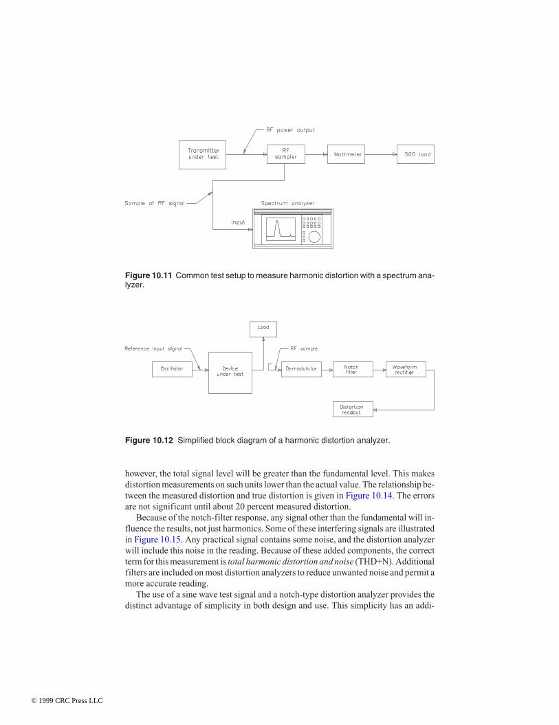
however, the total signal level will be greater than the fundamental level. This makesdistortion measurements on such units lower than the actual value. The relationship be-tween the measured distortion and true distortion is given in Figure 10.14. The errorsare not significant until about 20 percent measured distortion.
Because of the notch-filter response, any signal other than the fundamental will in-fluence the results, not just harmonics. Some of these interfering signals are illustratedin Figure 10.15. Any practical signal contains some noise, and the distortion analyzerwill include this noise in the reading. Because of these added components, the correctterm for this measurement is total harmonic distortion and noise (THD+N). Additionalfilters are included on most distortion analyzers to reduce unwanted noise and permit amore accurate reading.
The use of a sine wave test signal and a notch-type distortion analyzer provides thedistinct advantage of simplicity in both design and use. This simplicity has an addi-
Figure 10.11 Common test setup to measure harmonic distortion with a spectrum ana-lyzer.
Figure 10.12 Simplified block diagram of a harmonic distortion analyzer.
© 1999 CRC Press LLC

tional benefit in ease of interpretation. The shape of the output waveform from anotch-type analyzer indicates the slope of the nonlinearity. Displaying the residualcomponents on the vertical axis of an oscilloscope and the input signal on the horizon-tal axis provides a plot of the deviation of the transfer characteristic from a best-fitstraight line. This technique is diagrammed in Figure 10.16. The trace will be a hori-zontal line for a perfectly linear device. If the transfer characteristic curves upward onpositive input voltages, the trace will bend upward at the right-hand side.
Figure 10.13 Typical test setup for measuring the harmonic and spurious output of atransmitter. The notch filter is used to remove the fundamental frequency to preventoverdriving the spectrum analyzer input and to aid in evaluation of distortion compo-nents.
Figure 10.14 Conversion graph for indicated distortion and true distortion.
© 1999 CRC Press LLC

Examination of the distortion components in real time on an oscilloscope allow ob-servation of oscillation on the peaks of the signal and clipping. This is a valuable tool inthe design and development of RF circuits, and one that no other distortion measure-ment method can fully match. Viewing the residual components in the frequency do-
Figure 10.15 Example of interference sources in distortion and noise measurements.
Figure 10.16 Transfer-function monitoring configuration using an oscilloscope and dis-tortion analyzer.
© 1999 CRC Press LLC

main by using a spectrum analyzer also reveals much information about the distortionmechanism inside the device or stage under test.
When measuring distortion at high frequencies, bandwidth limitations are an im-portant consideration, as illustrated in Figure 10.17. Because the components beingmeasured are harmonics of the input frequency, they may fall outside the passband ofthe device under test.
Intermodulation Distortion
Intermodulation distortion (IMD) describes the presence of unwanted signals that arecaused by interactions between two or more desired signals. IMD, as it applies to anRF amplifier, refers to the generation of spurious products in a nonlinear amplifyingstage. IMD can be measured using a distortion monitor or a spectrum analyzer.
Nonlinearities in a circuit can cause it to act like a mixer, generating the sum and dif-ference frequencies of two signals that are present. These same imperfections generateharmonics of the signals, which then can be mixed with other fundamental or harmonicfrequencies. Figure 10.18 shows the relationship of these signals in the frequency do-main. The order of a particular product of IMD is defined as the number of “steps” be-tween it and a single fundamental signal. Harmonics add steps. For example, the secondharmonic = 2f1 = f1 + f1, which is two steps, making it a second-order product. The prod-uct resulting from 2f1 – f2 is, then, a third-order product. Some of the IMD products re-sulting from two fundamental frequencies include:
Figure 10.17 Illustration of problems that occur when measuring harmonic distortion inband-limited systems.
© 1999 CRC Press LLC

second-order = 2f1 (10.6)
= 2f2 (10.7)
= f1 + f2 (10.8)
= f1 – f2 (10.9)
third-order = 2f1 + f2 (10.10)
= 2f1 – f2 (10.11)
= 2f2 + f1 (10.12)
= 2f2 – f1 (10.13)
and so on.The order is important because, in general, the amplitudes of IMD products fall off
as the order increases. Therefore, low-order IMD products have the greatest potential tocause problems if they fall within the band of interest, or on frequencies used by otherservices or equipment. Odd-order IMD products are particularly troublesome becausethey fall closest to the signals that cause them, usually within the operating frequencyband.
Measurement Techniques
A number of techniques have been devised to measure the intermodulation (IM) oftwo or more signals passing through a device simultaneously. The most common of
Figure 10.18 Frequency-domain relationships of the desired signals and low-orderIMD products.
© 1999 CRC Press LLC

these involves the application of a test waveform consisting of a low-frequency signaland a high-frequency signal mixed in a specified amplitude ratio. The signal is ap-plied to the device under test, and the output waveform is examined for modulation ofthe upper frequency by the low-frequency signal. The amount by which the low-fre-quency signal modulates the high-frequency signal indicates the degree ofnonlinearity. As with harmonic distortion measurement, this test may be done with aspectrum analyzer or a dedicated distortion analyzer. The test setup for a spectrum an-alyzer is shown in Figure 10.19. Two independent signal sources are connected usinga power combiner to drive the device under test. The sources are set at the same outputlevel, but at different frequencies. A typical spectrum analyzer display of the two-tonedistortion test is shown in Figure 10.20. As shown, the third-order products that fallclose to the original two tones are measured. This measurement is a common, and im-portant, one because such products are difficult to remove by filtering.
The mechanisms of intermodulation as applied to interfering radiated signals arediscussed later in this chapter.
Addition and Cancellation of Distortion Components
The addition and cancellation of distortion components in test equipment or the de-vice under test is an often-overlooked problem in measurement. Consider the exam-ples in Figure 10.21 and 10.22. Assume that one device under test has a transfer char-acteristic similar to that diagrammed at the top left of Figure 10.21a, and another hasthe characteristic diagrammed at the center. If the devices are cascaded, the resultingtransfer-characteristic nonlinearity will be magnified as shown. The effect on sinewaves in the time domain is illustrated in Figure 10.21b. The distortion componentsgenerated by each nonlinearity are in phase and will sum to a component of twice theoriginal magnitude. However, if the second device under test has a complementarytransfer characteristic, as shown in Figure 10.22, quite a different result is obtained.When the devices are cascaded, the effects of the two curves cancel, yielding astraight line for the transfer characteristic (Figure 10.22a). The corresponding distor-
Figure 10.19 Test setup for measuring the intermodulation distortion of an RF amplifierusing a spectrum analyzer.
© 1999 CRC Press LLC

Figure 10.20 Typical two-tone IMD measurement, which evaluates the third-orderproducts within the bandpass of the original tones.
Figure 10.21 Illustration of the addition of distortion components: (a) addition of trans-fer-function nonlinearities, (b) addition of distortion components.
(b)
(a)
© 1999 CRC Press LLC

tion products are out of phase, resulting in no measured distortion components in thefinal output (Figure 10.22b).
This problem is common at low levels of distortion, especially between the testequipment and the device under test. For example, if the test equipment has a residual of0.002 percent when connected to itself, and readings of 0.001 percent are obtained fromthe circuit under test, cancellations are occurring. It is also possible for cancellations tooccur in the test equipment itself, with the combined analyzer and signal generator giv-ing readings lower than the sum of their individual residuals. If the distortion is the re-sult of even-order (asymmetrical) nonlinearity, reversing the phase of the signal be-tween the offending devices will change a cancellation to an addition. If the distortion isthe result of an odd-order (symmetrical) nonlinearity, phase inversions will not affectthe cancellation.
Intermodulation Precorrection Techniques
In a practical system, amplifiers cannot be absolutely linear; all linear amplifiers ex-hibit intermodulation distortion to some extent, relative to the amplitudes of the par-ent signals [1]. Adequate linearity is judged by the application, but in general, thein-band odd-order products should be as low as the state of the art permits becausethey are in-band and thus cannot be filtered out.
All intermodulation products are the result of undesirable time domain multiplica-tion of the matrix of input signals to a linear amplifier. All harmonic components arethe result of the same process, only here, an individual signal is multiplied by itself. For
Figure 10.22 Illustration of the cancellation of distortion components: (a) cancellation oftransfer-characteristic nonlinearities, (b) cancellation of the distortion waveform.
(b)
(a)
© 1999 CRC Press LLC

second order intermodulation, the ideal linear amplifier is modified by modeling a sin-gle mixer feeding a time domain multiplied signal around the amplifier. For third orderintermodulation, the ideal linear amplifier is modified by modeling two mixers feedinga time domain multiplied signal around the amplifier, as shown in Figure 10.23.
Because conventional amplitude modulation contains at least three parent signals(the carrier plus two sidebands), AM amplification has always been fraught within-band intermodulation distortion. A common technique to correct for these distortionproducts is to precorrect the power amplifier using the following process:
• Intentionally generate an anti-intermodulation signal by mixing the three inputsignals together
• Adjust the amplitude of the anti-IM product to match that of the real IM product
• Invert the phase
• Delay the correction signal or the parent signals in time so as to permit properalignment
• Add the correction signal into the main parent signal path to cause cancellation inthe output circuit of the amplifier
This is a well-known technique used in countless applications.Each intermodulation product may have its own anti-intermodulation product inten-
tionally generated to cause targeted cancellation. Even if one or more parent signalscontains modulation of some type—AM, FM, or PM—the legitimate modulation sig-nal is often included in the intended mixing circuit so that even the sidebands producedaround an intermodulation distortion product are canceled.
The precorrection circuit typically consists of mixer devices with a local oscillator(LO) port, an RF port, and an IF port. The LO port is fed with the parent signal, such asthe carrier, which contains no modulation. Its purpose is to hard-switch the mixer di-
Figure 10.23 Basic model of an intermodulation correction circuit. (After [1].)
© 1999 CRC Press LLC

odes, causing frequency translation of the signal fed to the RF port to the sum and dif-ference frequencies of the LO and RF input signals exiting at the IF port. Theintermodulation product to be canceled is either a result of the sum or the difference sig-nal so that the product of no concern is filtered out. The resulting intended mixer prod-uct is fed to the IF port of a second mixer where LO injection is from the third parentsignal. The third order intended mixing product is then available at the second mixer RFport, and will be at the frequency of the offending IM and coherent with it.
Digital signals suitable for radio transmission actually remain analog, but aretermed digital because of the nature of the information that they carry. A modern digitalradio transmission using quadrature amplitude modulation (QAM) or n-level vestigialsideband modulation (e.g., 8-VSB) consists of a vector signal constantly moving inphase angle and magnitude relative to some reference. The vector signal is smooth andwithout discontinuity so that it is well contained within a finite bandwidth. Its digitalnature stems from decoding the proper point or spatial area around a point (QAM) of a
Figure 10.24 Digital decoding process: (a) 16-QAM, (b) 8-VSB. (After [1].)
(b)
(a)
© 1999 CRC Press LLC

finite number of legitimate points, or the proper line (VSB) or spatial area around a lineof a finite number of legitimate lines, that the vector is passing though. Figure 10.24 il-lustrates this process. In either case, the area is assigned a discrete digital value, whichrepresents a portion of the information being transmitted. Spatial location is generallyexpressed in terms of rectangular coordinates with I (in phase) and Q (quadraturephase) components.
Because the vector appears to move at random from point to point, especially result-ing from the use of an intentional randomizer circuit, the frequency distribution withinthe passband of the signal is constant, flat, and favors no particular frequency. Figure10.25 illustrates the frequency distribution with the sidebands shown before and afteramplification. As a result, the transmitted signal is said to be “noise-like.” As such, ittakes on the nature of noise and need not be periodic.
For this case, there is no identifiable set of parent components upon which to obtainsignals for the purpose of mixing to generate an anti-intermodulation signal for cancel-lation purposes. There is no carrier signal to feed into the LO port of a mixer for hardswitching to generate sum and difference frequencies. Because the signal is noise-like,there is no correlation of any piece of passband spectrum with any other. Generating aprecorrection signal, thus, is not possible using the process described for the discretesignal analog case.
10.3 Vacuum Tube Operating ParametersDirect current input power to the final RF output stage is a function of the appliedplate or collector voltage and the plate or collector current of the final tube(s) [2]. Testpoints or built-in meters usually are provided for checking the dc voltage and currentlevels of the final amplifier.
Transmitter deviation or modulation must be set properly. A deviation level set toohigh or too low adversely affects radio range. If the deviation is set too low, the sig-
Figure 10.25 Digitally modulated RF signal spectrum before and after amplification.(After [1].)
© 1999 CRC Press LLC

nal-to-noise ratio of the overall system is diminished. If the deviation is set too high, thetransmitter signal may exceed the receiver’s modulation acceptance bandwidth, caus-ing severe distortion on modulation peaks and out-of-band spurious radiation.
The difference between the positive and negative excursions of the deviated wave-form is defined as modulation dissymmetry. Theoretically, positive and negative excur-sions should be perfectly symmetrical. In practice, however, there is usually somedissymmetry. In a multichannel phase-modulated transmitter, modulationdissymmetry may be worse on some channels than others as a result of modulator tun-ing. If the modulator tuning is peaked on one channel, for example, response on anotherchannel may be compromised.
10.3.1 Stage Tuning
A power output stage can be tuned in any number of ways [2]. Determining factors in-clude the type of device, circuit design, and operational objectives. A PA can be tunedto optimize bandwidth, linearity, efficiency, and other parameters. It is often neces-sary to compromise one parameter to enhance another. This tradeoff is dictated by theapplication.
Power Grid Tubes
When optimizing a tetrode or pentode RF amplifier for proper excitation and loading,the general tuning procedure varies depending upon whether the screen voltage istaken from a fixed supply or a dropping resistor supply with poor regulation [2]. Ifboth the screen supply and grid bias are from fixed sources with good regulation, theplate current is almost entirely controlled by RF excitation. The loading is then varieduntil the maximum power output is obtained. Following these adjustments, the excita-tion is trimmed, along with the loading, until the desired control and screen grid cur-rents are obtained.
In the case of an RF amplifier where both the screen and grid bias are taken fromsources with poor regulation, the stage will tune in a manner similar to a triode RFpower amplifier. The plate current will be controlled principally by varying the load-ing, and the excitation trimmed to yield the desired control grid current. In this case, thescreen current will be almost entirely set by the choice of the dropping resistor. Excita-tion and loading will vary the screen voltage considerably, and these should be trimmedto yield a desired screen voltage.
The grounded-grid amplifier has been used for many years, and, with the advent ofhigh-power zero-bias triodes, this configuration has become more common. Adjust-ment of the excitation and loading of a grounded-grid RF amplifier requires a slightlydifferent procedure. The plate voltage (plate and screen voltage in the case of a tetrodeor pentode) must be applied before the excitation. If this precaution is not followed, thecontrol grid may sustain damage. The loading is increased as the excitation is in-creased. When the desired plate current is reached, note the power output. The loadingcan be reduced slightly and the excitation increased until the plate current is the same asbefore. If the power output is less than before, a check can be made with increased load-
© 1999 CRC Press LLC

ing and less excitation. By proper trimming, the proper grid current, plate current, andoptimum power output can be obtained. In a grounded-grid circuit, the cathode or inputcircuit is in series with the plate circuit. Because of this arrangement, any change madein the plate circuit will affect the input circuit. Therefore, the driver amplifier does notsee its designed load until the driven stage is up to full plate current.
Typical operating values provide a starting point for tuning efforts. As long as themaximum limits are not exceeded, a wide range of tuning options is available.
Screen Voltage
Typical operating values given on the data sheet for tetrode and pentode devices in-clude recommended screen voltages [2]. These values are not critical for most appli-cations; they are chosen as a convenient value consistent with low driving power andreasonable screen dissipation. If lower values of screen voltage are used, more drivingvoltage will be required on the grid to obtain the same plate current. If higher valuesof screen voltage are used, less driving voltage will be required. Thus, high powergain can be achieved, provided the circuit exhibits adequate stability. Be careful not toexceed the screen dissipation limit. The value of screen voltage can be chosen to suitavailable power supplies or amplifier conditions.
The published characteristic curves of tetrodes and pentodes are shown for com-monly used screen voltages. Occasionally, it is desirable to operate the tetrode orpentode at some screen voltage other than that shown on the characteristic curves. It is arelatively simple matter to convert the published curves to corresponding curves at adifferent screen voltage. This conversion is based on the fact that if all interelectrodevoltages are either raised or lowered by the same relative amount, the shape of the volt-age field pattern is not altered, and neither is the current distribution. The current linessimply take on new proportionate values in accordance with the three-halves powerlaw. This method fails only where insufficient cathode emission or high secondaryemission affects the current values.
For example, if the characteristic curves are shown at a screen voltage of 250 V and itis desirable to determine conditions at 500 V on the screen, all voltage scales should bemultiplied by the same factor that is applied to the screen voltage (2 in this case). The 1kV plate voltage line thus becomes 2 kV, the 50 V grid voltage line becomes 100 V, andso on. All current lines then assume new values in accordance with the 3/2 power law.Because the voltage was increased by a factor of 2, the current lines all will be increasedin value by a factor of 23/2 or 2.8. All current values are then multiplied by the factor of2.8. The 100 mA line thus becomes a 280 mA line, and so on.
Likewise, if the screen voltage given on the characteristic curve is higher than theconditions desired, the voltage should be reduced by the same factor that is used to ob-tain the desired screen voltage. Correspondingly, the current values all will be reducedby an amount equal to the 3/2 power of this factor. Commonly used factors are given inTable 10.2.
© 1999 CRC Press LLC

Back-Heating by Electrons
Back-heating of the cathode is an undesirable action involving the motion of electronswithin the tube at VHF and UHF [2]. Because the time of flight of electrons from thecathode through the grid structure to the plate becomes an appreciable part of the cy-cle at high frequencies, electrons can be stopped in flight and turned back by the rap-idly changing grid voltage. Under these conditions, the electrons are deflected fromtheir normal paths and given excess energy with which they bombard the cathode andother portions of the tube structure. This effect can be aggravated by the choice of op-erating conditions to the extent that destructive effects occur. The tube can be de-stroyed within a few minutes under severe conditions.
Fortunately, the conditions that tend to minimize this back-bombardment by elec-trons also characterize minimum driving voltage. The tendency of electrons to turnback in flight is reduced by using the lowest possible RF grid voltage on the tube. This isachieved by using the lowest possible dc grid bias. In tetrodes, this effect is inherentlylower because of the action of the screen in accelerating the electrons toward the anode.A tetrode also permits the use of smaller grid voltages. Consequently, under favorableconditions, the number of electrons turned back to heat the cathode and tube structurecan be kept to a practical, low level. In addition to low dc grid bias, high screen voltageis desirable.
The plate circuit should always operate with heavy loading (low external plate im-pedance) so that the minimum instantaneous value of plate voltage will stay suffi-ciently positive to continue accelerating electrons to the anode. For this reason, the lon-gest tube life is realized when the tetrode amplifier is heavily loaded, as indicated byhaving small values of dc screen and dc control grid current.
Voltage Factor Current Factor0.25 0.1250.50 0.350.75 0.651.00 1.001.25 1.401.50 1.841.75 2.302.00 2.802.25 3.402.50 4.002.75 4.603.00 5.20
Table 10.2 Three-Halves Current Values of Commonly Used Factors
© 1999 CRC Press LLC

Never operate a tube with light plate loading. If the plate load is removed so that theminimum instantaneous plate voltage tends to fall to values approximating cathode po-tential (as it must do when the loading is removed completely and excitation is present),the number of electrons turned back can be destructive to the tube. It has been foundthat under conditions of no loading, the electron bombardment and increased electricfield heating of the insulating portion of the tube is often sufficient to cause suck-in ofthe glass or cracking of the ceramic envelope. Automatic protection should be providedto remove all voltages from the tube if the plate circuit loading becomes too light for theamount of excitation applied.
Note that parasitic oscillations seldom are loaded heavily, as indicated by the highgrid currents often observed during such self-oscillation. Thus, excessive RF platevoltages are developed that, at VHF, can be as damaging as unloaded operation on aVHF fundamental frequency. If unloaded VHF parasitic oscillations are present simul-taneously with apparently satisfactory operation on the fundamental, unexplained re-duction of tube life may result.
Occasionally, an output line circuit may resonate simultaneously to a harmonic fre-quency as well as to the fundamental frequency. The higher resonant modes of practicalline circuits are not normally harmonically related. Sometimes, however, the tuningcurve of a mode will cross the fundamental tuning curve and, at that point, the circuitwill build up resonant voltages at both the harmonic and the fundamental frequency.The harmonic resonance usually is lightly loaded and the damaging action is similar tothat of lightly loaded parasitic or fundamental. Again, while operation of the tube andcircuit on the fundamental may appear normal, but with lower than expected efficiency,damage can occur to the tube.
In addition to operating the tube with minimum bias, high screen voltage, and heavyloading on the plate circuit, some degree of compensation for the remaining back-heat-ing of the cathode may be required. This can be accomplished by lowering the filamentvoltage or heater voltage until the cathode operates at a normal temperature. In the caseof tetrodes and pentodes, by taking precautions necessary to minimize back-bombard-ment by electrons, the required compensation for back-heating of the cathode is not sig-nificant and may often be neglected.
10.3.2 Amplifier Balance
In a push-pull RF amplifier, lack of balance in the plate circuit or unequal plate dissi-pation usually is caused by a lack of symmetry in the RF circuit [2]. Normally, thetubes are similar enough that such imbalance is not associated with the tubes and theircharacteristics. This can readily be checked by interchanging the tubes in the sockets(provided both tubes have common dc voltages to plate, screen, and grid) and observ-ing whether the unbalanced condition remains at the socket location or moves withthe tube. If it remains at the socket location, the circuit requires adjustment. If appre-ciable imbalance is associated with the tube, it is likely that one tube is abnormal andshould be replaced.
The basic indicators of balance are the plate current and plate dissipation of eachtube. It is assumed that the circuit applies the same dc plate voltage, dc screen voltage
© 1999 CRC Press LLC

(in the case of a tetrode or pentode), and dc grid bias to each tube from common sup-plies. Also, it is initially assumed that the plate circuit is mechanically and electricallysymmetrical (or approximately so).
Imbalance in a push-pull RF amplifier is usually the result of unequal RF voltagesapplied to the grids of the tubes, or the RF plate circuit applying unequal RF voltages tothe plates of the tubes. Correction of this situation involves first balancing grid excita-tion until equal dc plate currents flow in each tube. Next, the RF plate circuit is adjusteduntil equal plate dissipation appears on each tube, or equal RF plate voltage is ob-served. The balance of plate current is a more important criterion than equality ofscreen current (in a tetrode or pentode) or grid current. This results from the fact thattubes tend to be more uniform in plate current characteristics. However, the screen cur-rent also is sensitive to a lack of voltage balance in the RF plate circuit and may be usedas an indicator. If the tubes differ somewhat in screen current characteristics, and thecircuit has common dc supply voltages, final trimming of the plate circuit balance maybe made by interchanging tubes and adjusting the circuit to give the same screen currentfor each tube, regardless of its location.
Note that the dc grid current has not been used as an indicator of balance of the RFpower amplifier. It is probable that after following the foregoing procedure, the gridcurrents will be fairly well balanced, but this condition, in itself, is not a safe indicatorof grid excitation balance.
10.3.3 Parallel Tube Amplifiers
The previous discussion has been oriented toward the RF push-pull amplifier. Thesame comments can be directed to parallel tube RF amplifiers [2]. Balance—the con-dition in which each tube carries its fair share of the load—still must be considered. Inlow-frequency amplifiers operating in class AB1 or class AB2, the idle dc plate currentper tube should be balanced by separate bias adjustments for each tube. In manycases, some lack of balance of the plate currents will have negligible effect on theoverall performance of the amplifier.
When tubes are operating in the idle position close to cutoff, an exact balance is dif-ficult to achieve because plate current cannot be held to a close percentage tolerance.At this point, the action of the plate and screen voltages is in delicate balance with theopposing negative grid voltage. The state of balance is indicated by the plate current.Minor variations of individual grid wires or variations in the diameter of grid wires canupset the balance. It is practically impossible to control such minor variations in manu-facture.
10.3.4 Harmonic Energy
A pulse of plate current delivered by the tube to the output circuit contains compo-nents of the fundamental and most harmonic frequencies [2]. To generate outputpower that is an harmonic of the exciting voltage applied to the control grid, it ismerely necessary to resonate the plate circuit to the desired harmonic frequency. Tooptimize the performance of the amplifier, it is necessary to adjust the angle of plate
© 1999 CRC Press LLC

current flow to maximize the desired harmonic. The shorter the length of the currentpulse, in the case of a particular harmonic, the higher the plate efficiency. However,the bias, exciting voltage, and driving power must be increased. Also, if the pulse istoo long or too short, the output power will decrease appreciably.
The plate circuit efficiency of tetrode and pentode harmonic amplifiers is quitehigh. In triode amplifiers, if feedback of the output harmonic occurs, the phase of thevoltage feedback usually reduces the harmonic content of the plate pulse, and therebylowers the plate circuit efficiency. Because tetrodes and pentodes have negligible feed-back, the efficiency of a harmonic amplifier usually is comparable to that of other am-plifier types. Also, the high amplification factor of a tetrode or pentode causes the platevoltage to have little effect on the flow of plate current. A well-designed tetrode orpentode also permits large RF voltages to be developed in the plate circuit while stillpassing high peaks of plate current in the RF pulse. These two factors help to further in-crease plate efficiency.
Controlling Harmonics
The previous discussion of harmonics has been for the case where harmonic power inthe load is the objective. The generation and radiation of harmonic energy must bekept to a minimum in a fundamental frequency RF amplifier [2]. The ability of thetetrode and pentode to isolate the output circuit from the input circuit over a widerange of frequencies is important in avoiding feedthrough of harmonic voltages fromthe grid. An important part of this shielding is the result of the basic physical designof the devices. The following steps permit reduction of unwanted harmonic energy inthe output circuit:
• Minimize the circuit impedance between plate and cathode. This objective maybe achieved by having some or all of the tuning capacitance of the resonant circuitclose to the tube.
• Completely shield the input and output compartments of the stage.
• Use inductive output coupling from the resonant plate circuit, and possibly a ca-pacitive or Faraday shield between the coupling coil and the tank coil. A high-fre-quency attenuating circuit, such as a Pi or Pi-L network, also may be used.
• Incorporate low-pass filters on all supply leads and wires leading to the outputand input compartments.
• Use resonant traps for particular frequencies as required.
• Install a low-pass filter in series with the output transmission line.
10.3.5 Klystron Tuning Considerations
The output power stability of a klystron is sensitive to changes in the principal operat-ing parameters, including:
• Beam input power
© 1999 CRC Press LLC

• RF drive power
• RF drive frequency
• Device tuning
• Magnetic fields in the vicinity of the tube
• VSWR of the load
Varying any of these parameters will affect the RF output power response.Figure 10.26 illustrates how changes in the dc beam input power affect the RF output
power of a klystron under constant RF drive conditions. Small changes in dc inputpower produce marked changes in RF output power. Figure 10.27 shows RF outputpower as a function of RF drive power applied to the tube. From this curve, it can beseen that when the RF drive power is low, the RF output power is low. As the level of RFdrive power increases, RF output power increases until an optimum operating point isreached. Beyond this point, further increases in RF drive power result in reduced RFoutput power.
Klystrons are said to be saturated at the point where a further increase in RF driveonly decreases the RF output power. To obtain maximum RF output from a klystron,sufficient RF drive must be applied to the tube to reach the point of saturation. Oper-ating at RF drive levels beyond saturation will only overdrive the klystron, decrease RFoutput power, and increase the amount of beam interception (body current) at the drifttube.
Figure 10.26 RF output power variation as a function of dc beam input power for a kly-stron.
© 1999 CRC Press LLC

Tuning of any cavity of a multicavity klystron will affect the overall shape of the am-plitude-response curve. There are two common methods of tuning klystrons:
• High-efficiency narrowband tuning
• Broadband tuning, yielding lower gain and efficiency
Figure 10.28 shows how RF output power changes with various levels of RF drive ap-plied to a klystron under different tuning conditions. The RF power at point A repre-sents the drive saturation point for a synchronously tuned tube. Point B shows a newpoint of saturation that is reached by tuning the penultimate (next to the last) cavity toa somewhat higher frequency. By tuning the penultimate cavity still further, point C isreached. At point D, increasing the penultimate cavity frequency no longer increasesRF output power; instead, it reduces the power delivered by the tube (curve E).
10.3.6 Intermodulation Distortion
Intermodulation distortion products in linear power amplifier circuits can be causedby either amplitude gain nonlinearity or phase shift with change in input signal level.Intermodulation distortion products appear when the RF signal has a varying enve-lope amplitude. A single continuous-frequency wave will be amplified by a fixedamount and shifted in phase by a fixed amount. The nonlinearity of the amplifier will
Figure 10.27 RF output power of a klystron as a function of RF drive power.
© 1999 CRC Press LLC

produce only harmonics of the input wave. As the input RF wave changes, thenonlinearity of the amplifier will cause undesirable intermodulation distortion.
When an RF signal with varying amplitude is passed through a nonlinear device,many new products are produced. The frequency and amplitude of each component canbe determined mathematically. The nonlinear device can be represented by a power se-ries expanded about the zero-signal operating point. Intermodulation distortion energyis wasted and serves no purpose other than to cause interference to adjacent channels.Intermodulation distortion in a power amplifier tube is principally the result of its trans-fer characteristics. An ideal transfer characteristic curve is shown in Figure 10.29.
Even-order products do not contribute to the intermodulation distortion problem be-cause they usually fall outside the amplifier passband. Therefore, if the transfer charac-teristic produces an even-order curvature at the small-signal end of the curve (frompoint A to point B) and the remaining portion of the curve (point B to point C) is linear,the tube is considered to have an ideal transfer characteristic. If the operating point ofthe amplifier is set at point 0 (located midway horizontally between point A and pointB), there will be no distortion in a class AB amplifier. However, no tube has this ideal-ized transfer characteristic. It is possible, by manipulation of the electron ballisticswithin a given tube structure, to alter the transfer characteristic and minimize the dis-tortion products.
Figure 10.28 Output power variation of a klystron as a function of drive power under dif-ferent tuning conditions.
© 1999 CRC Press LLC

Generation of RF Intermodulation Products
When two or more transmitters are coupled to each other, new spectral componentsare produced by mixing of the fundamental and harmonic terms of each of the desiredoutput frequencies.1 The most common form of coupling results from transmitting an-tennas that are physically closely spaced. If sufficient filtering is not provided at theoutput stages and/or on one or both of the transmitter feedlines, energy from onetransmitter may travel back to the final power amplifier of the other. In the PA stage,the desired and undesired signals mix, producing spurious intermodulation products.
Consider the following example involving two transmitters. The third-orderintermodulation products (IM3) are generated in the following manner:
• The output of transmitter 1 (f1) is coupled into the nonlinear output stage of trans-mitter 2 (f2). This condition is the result of insufficient isolation between the twooutput signals.
• Signal f1 mixes with the second harmonic of f2, producing an in-band third-orderterm with a frequency of 2f2 – f1 at the output of transmitter 2.
• In a similar manner, another third-order term will be produced at a frequency of2f1 – f2 at the output of transmitter 1.
Figure 10.29 Ideal grid-plate transfer curve for class AB operation.
1 Portions of this section were contributed by Geoffrey N. Mendenhall, P. E., Cincinnati, OH.
© 1999 CRC Press LLC

This implies that the second-harmonic content within the output stage of each trans-mitter, along with the specific nonlinear characteristics of the output stage, will havean effect on the value of the mixing loss.
It is also possible to generate these same third-order terms in another way. If the dif-ference frequency between the two transmitters (f2 – f1), which is an out-of-band fre-quency, remixes with either f1 or f2, the same third-order intermodulation frequencieswill be produced.
Empirical measurements [3] indicate that the 2f2 – f1 type of mechanism is the domi-nant mode generating third-order IM products in RF generators using a tuned cavity forthe output network. Figure 10.30 illustrates the mechanism of third-order IM for thetwo-signal condition.
IM As a Function of Turnaround Loss2
Turnaround or mixing loss describes the phenomenon whereby the interfering signalmixes with the fundamental and its harmonics within the nonlinear output device.This mixing occurs with a net conversion loss; hence, the term turnaround loss hasbecome widely used to quantify the ratio of the interfering level to the resulting IM3level. A turn around loss of 10 dB means that the IM3 product fed back to the antennasystem will be 10 dB below the interfering signal fed into the transmitter output stage.
Turnaround loss will increase if the interfering signal falls outside the passband ofthe transmitter output circuit, varying with frequency separation of the desired signal
Figure 10.30 Frequency spectrum of third-order IM with the interfering level equal tothe carrier level.
2 Mendenhall, Geoffrey N., “A Study of RF Intermodulation Between FM BroadcastTransmitters Sharing Filterplexed or Colocated Antenna Systems, Broadcast Electronics,Quincy, Il, 1983.
© 1999 CRC Press LLC

and the interfering signal. This is because the interfering signal is first attenuated by theoutput circuit selectivity going into the nonlinear device, then the IM3 product is fur-ther attenuated as it comes back through the frequency-selective circuit. Turnaroundloss, thus, can be divided into three principal components:
• The basic in-band conversion loss of the nonlinear device
• Attenuation of the out-of-band interfering signal resulting from the selectivity ofthe output stage
• Attenuation of the resulting out-of-band IM3 products resulting from the selec-tivity of the output circuit
As the turnaround loss increases, the level of undesirable intermodulation products isreduced, and the amount of isolation required between the transmitters also is re-duced.
Transmitter output circuit loading directly affects the power amplifier source im-pedance and, therefore, also affects the efficiency of coupling the interfering signal intothe output circuit where it mixes with the other frequencies present to yield IM3 prod-ucts. Light loading reduces the amount of interference that enters the output circuitwith a resulting increase in turnaround loss. In addition, output loading will change theoutput circuit bandwidth (loaded Q) and, therefore, also affect the amount of attenua-tion that out-of-band signals will encounter in passing into and out of the output circuit.
Second-harmonic traps or low-pass filters in the transmission line of either trans-mitter have little effect on the generation of IM products. This is because the harmoniccontent of the interfering signal entering the output circuit of the transmitter has muchless effect on IM3 generation than the harmonic content within the nonlinear device it-self. The interfering signal and the resulting IM3 products thus fall within the passbandof the low-pass filters and outside the reject band of the second-harmonic traps; thesedevices typically offer little, if any, attenuation to RF intermodulation products.
Site-related intermodulation problems and typical solutions are discussed later inthis chapter.
10.3.7 VSWR
Among all the possible load measurements, VSWR is the most common. An in-linedirectional wattmeter commonly is used to measure both the forward and reflectedpower in a feedline. It is the comparison of reflected power (Pr) to forward power (Pf)that provides a qualitative measure of the match between a transmitter and itsfeedline/load.
The standing wave ratio (SWR) on a transmission line is related to the ratio of the for-ward to reflected power by the following:
© 1999 CRC Press LLC

SWR =
1
1
+
−
PP
PP
r
f
r
f
(10.14)
The standing wave is the result of the presence of two components of power: onetraveling toward the load and the other reflected by a load mismatch, traveling back to-ward the generator. These components are defined by the following:
( )PE
ZI Zf
f
o
f o= =2
2 (10.15)
( )PE
ZI Zr
r
o
r o= =2
2 (10.16)
( )P P Pn f r= − (10.17)
Where:Pf = forward powerPr = reflected powerEf = forward voltageEr = reflected voltageIf = forward currentIr = reflected currentZo = characteristic impedance of the linePn = net power absorbed by the load (transmission line loss and antenna radiation)
Because the forward and reflected voltages and currents are traveling in opposite di-rections, they will add in phase at some point along the line to produce a voltage maxi-mum. At wavelength along the line in either direction from this maximum, the forwardand reflected components will be out of phase, and will produce a voltage minimum.The forward and reflected components of current also add vectorally to produce a cur-rent standing wave. The magnitude of this wave is defined by:
SWR =E
E
I
Imax
min
max
min
= (10.18)
The ratio of the highest voltage point on the line to the lowest voltage point on theline commonly is used to evaluate system performance. This property is known as thevoltage standing wave ratio (VSWR). A VSWR of 1.0:1.0 means that a perfect matchhas been achieved. A VSWR of 2.0:1.0 means that a mismatch is causing power to bereflected back from the load, approximately 11 percent in this particular case.
© 1999 CRC Press LLC

At the point of reflection (the load mismatch), the phase of the reflected current is re-versed 180° from the forward current. The reflected voltage does not exhibit this phasereversal. This displaces the voltage and current standing waves by 90° along the line sothat the Emax and Imin occur at the same points, while Emin and Imax occur 90° in either direc-tion from Emax and Imin.
The fact that the reflected current is reversed in phase makes it possible to measureforward and reflected power separately using a directional coupler device. A small volt-age is obtained by inductive coupling that represents the current in the transmissionline. To this signal is added a sample of the voltage across the line, simultaneously ob-tained by capacitive coupling. These two samples are adjusted to be exactly equal whenthe line is terminated with its characteristic impedance. The two RF samples, whenadded, yield a resultant RF voltage proportional to the forward components of voltageand current. Reflected power is measured by installing a second coupling section physi-cally turned in the opposite direction. The phase of the current sample is reversed, andthe reflected components add while the forward components balance out.
On a theoretical, lossless feedline, VSWR is the same at all points along the line.Actually, all feedlines have some attenuation distributed uniformly along their entirelengths. Any attenuation between the reflection point and the source reduces VSWR atthe source. This concept is illustrated in Figure 10.31. Standing waves on the feedlineincrease feedline attenuation to a level greater than normal attenuation undermatched-line conditions. The amount of feedline attenuation increase depends on theVSWR and the extent of losses under matched-line conditions. The higher thematched-line attenuation, the greater the additional attenuation caused by a givenVSWR. Figure 10.32 correlates additional attenuation with matched-line attenuationfor various VSWR levels.
When a feedline is terminated by an impedance equal to the feedline characteristicimpedance, the feedline impedance at any point is equal to the feedline characteristicimpedance. When the feedline is terminated by an impedance not equal to the feedlinecharacteristic impedance, the feedline input impedance will vary with changes infeedline length. The greater the impedance mismatch at the load, the wider the feedlineinput impedance variation with changes in line length. The largest feedline impedancechange occurs with the worst mismatches: open circuit or short circuit.
A short circuit at the end of a feedline appears as an open circuit at a point wave-length down the feedline. It is the greatest impedance transformation that can occur ona feedline. Less severe mismatches cause smaller impedance transformations. At apoint wavelength down the line, the impedance equals the load impedance. Feedlineswith high VSWR sometimes are called resonant or tuned feedlines. Matchedlines—those with little VSWR—are referred to as nonresonant or untuned feedlines.This phenomenon means that high feedline VSWR can cause the feedline input to pres-ent a load impedance to the output tube that differs greatly from the feedline character-istic impedance. Some RF generators incorporate an output matching network that pro-vides a conjugate match to a broad range of impedances.
© 1999 CRC Press LLC

10.4 RF System PerformanceAssessing the performance of an RF generator has been greatly simplified by recentadvancements in system design. The overall performance of most transmitters can beassessed by measuring the audio, video, or data performance of the system as awhole. If these “intelligence signal” tests indicate good performance, chances aregood that all of the RF parameters also meet specifications. Both AM and FM trans-mission systems have certain limitations that prevent them from ever being a com-pletely transparent medium. Through proper system design and regular equipmentmaintenance, however, overall performance can be maintained at acceptable levels inmost operational environments.
Figure 10.31 Illustration of how the VSWR on a transmission line affects the attenua-tion performance of the line. Scale A represents the VSWR at the transmitter; scale Brepresents the corresponding reflected power in watts for an example system.
© 1999 CRC Press LLC

10.4.1 Key System Measurements
The procedures for measuring transmitter performance vary widely, depending on thetype of equipment being used. Certain basic measurements, however, can be appliedto characterize the overall performance of most systems:
• Frequency response: the actual deviation from a constant amplitude across agiven span of frequencies.
• Total harmonic distortion: the creation, by a nonlinear device, of spurious signalsharmonically related to the applied waveform. THD is sensitive to the noise floorof the system under test. If the system has a signal-to-noise ratio of 60 dB, the dis-tortion analyzer’s best possible reading will be higher than 0.1 percent (60 dB =0.001 = 0.1 percent).
• Intermodulation distortion: the creation, by a nonlinear device, of spurious sig-nals not harmonically related to the audio waveform. These distortion compo-nents are sum-and-difference (beat note) mixing products. The IM measurementis relatively impervious to the noise floor of the system under test.
Figure 10.32 Illustration of how VSWR causes additional loss in a length of feedline.
© 1999 CRC Press LLC

• Signal-to-noise ratio (S/N): the amplitude difference, expressed in decibels, be-tween a reference-level audio signal and the residual noise and hum of the overallsystem.
• Crosstalk: the amplitude difference, expressed in decibels, between two or morechannels of a multichannel transmission system.
10.4.2 Synchronous AM in FM Systems3
The output spectrum of an FM transmitter contains many sideband frequency compo-nents, theoretically an infinite number. The practical considerations of transmitter de-sign and frequency allocation make it necessary to restrict the bandwidth of FM sig-nals. Bandwidth restriction brings with it a number of undesirable side effects, includ-ing:
• Phase shifts through the transmission chain
• Generation of synchronous AM components
• Distortion in the demodulated output of certain receivers
In most medium- and high-power FM transmitters, the primary out-of-band filteringis performed in the output cavity of the final stage. Previous stages in the transmitter(the exciter and IPA) are designed to be broadband, or at least more broadband thanthe PA. As the bandwidth of an FM transmission system is reduced, synchronous am-plitude modulation increases for a given carrier deviation (modulation). SynchronousAM is produced as tuned circuits with finite bandwidth are swept by the frequency ofmodulation. The amount of synchronous AM generated is dependent on tuning,which determines (to a large extent) the bandwidth of the system. Figure 10.33 illus-trates how synchronous AM is generated through modulation of the FM carrier.
Bandwidth Limiting
The design goal of most medium- and high-power FM transmission equipment is tolimit the bandwidth of the transmitted RF signal at one stage only. In this way, controlover system bandwidth can be tightly maintained, and the tradeoffs required in anypractical FM system can be optimized. If, on the other hand, more than onenarrowband stage exists within the transmitter, adjustment for peak efficiency andperformance can be a difficult proposition. The following factors can affect the band-width of an FM system:
• Total number of tuned circuits in the system
3 Mendenhall, Geoffrey N., “Techniques for Measuring Synchronous AM Noise in FMTransmitters,” Broadcast Electronics, Quincy, IL, 1988.
© 1999 CRC Press LLC

• Amplitude and phase response of the total combination of all tuned circuits in theRF path
• Amount of drive to each RF stage (saturation effects)
• Nonlinear transfer function within each RF stage
The following techniques can be used to improve the bandwidth of a given system:
• Maintain wide bandwidth until the final RF stage. This can be accomplishedthrough the use of a broadband exciter and broadband (usually solid-state) IPA.
• Minimize the number of interactive-tuned networks within the system. Throughproper matching network design, greater bandwidth and simplified tuning can beaccomplished.
Bandwidth affects the gain and efficiency of any FM RF amplifier. The bandwidthis determined by the load resistance across the tuned circuit and the output or input ca-pacitance of the RF stage. Because grid-driven PA tubes typically exhibit high input ca-pacitance, the PA input circuit generally has the greatest effect on bandwidth limiting inan FM transmitter. The grid circuit can be broadened through resistive swamping in theinput circuit, or through the use of a broadband input impedance matching network.One approach involves a combination of series inductor and shunt capacitor elements
Figure 10.33 The generation of synchronous AM in a bandwidth-limited FM system.Note that minimum synchronous AM occurs when the system operates in the center ofits passband.
© 1999 CRC Press LLC

implemented on a printed wiring board, as illustrated in Figure 10.34. In this design, theinductors and capacitors are etched into the copper-clad laminate of the PWB. This ap-proach provides the necessary impedance transformation from a 50 Ωsolid-state driverto a high-impedance PA grid in a series of small steps, rather than more conventional L,Pi, or Tee matching networks.
Effects of Synchronous AM
The effect of bandwidth on synchronous AM performance for an example FM RFamplifier is plotted in Figure 10.35. Notice that as the –3 dB points of the RF systempassband are narrowed, a dramatic increase in synchronous AM occurs. The effectshown in the figure is applicable to any bandwidth-limited FM system.
Bandwidth also affects the distortion floor of the demodulated signal of an FM sys-tem, as plotted in Figure 10.36. The data shown apply to a test setup involving a sin-gle-tuned circuit fed by an FM generator with a deviation of ±75 kHz at a modulatingfrequency of 15 kHz (no de-emphasis is applied to the output signal). Remember thatFM is a nonlinear process and that interpretation of distortion numbers for multi-ple-carrier signals is not accurate. The example shown, however, illustrates how thebandwidth of the RF channel can set a minimum performance limit on system total har-monic distortion. By understanding the mechanics of synchronous AM, adjustment foroptimum performance of an FM system can be accomplished.
10.4.3 Incidental Phase Modulation
Incidental phase modulation (IPM) is phase modulation produced by an AM trans-mitter as a result of amplitude modulation. In other words, as an AM transmitter de-velops the amplitude-modulated signal, it also produces a phase-modulated, or PM,version of the input intelligence. In theory, IPM is of little consequence for classicAM applications because FM and PM do not affect the carrier amplitude. An enve-lope detector will, in theory at least, ignore IPM. However, a number of applicationsutilize manipulation of the carrier phase to convey information in addition to ampli-tude modulation of the carrier. Receivers designed to decode such AM/PM wave-forms will not perform properly if excessive IPM is produced by the transmitter. Al-
Figure 10.34 IPA plate-to-PA-grid matching network designed for wide bandwidth op-eration.
© 1999 CRC Press LLC

though the effects of IPM vary from one system to another, optimum performance isrealized when IPM is minimized.
As a general rule, because IPM is a direct result of the modulation process, it can begenerated in any stage that is influenced by modulation. The most common cause ofIPM in plate-modulated and pulse-modulated transmitters is improper neutralizationof the final RF amplifier. Adjusting the transmitter for minimum IPM is an accurateway of achieving proper neutralization. The reverse is not always true, however, be-cause some neutralization methods will not necessarily result in the lowest IPM.
Improper tuning of the IPA stage is the second most common cause of IPM. As mod-ulation changes the driver loading to the PA grid, the driver output also may vary. Thecircuits that feed the driver stage usually are sufficiently isolated from the PA that theydo not produce IPM. An exception is if the power supply for the IPA is influenced bymodulation. Such a problem could be caused by a lack of adequate capacitance in thefilters of the high-voltage power supply.
Bandwidth Considerations
When a perfect AM transmitter is modulated with a tone, two sidebands are created,one above the carrier and one below it. Phase modulation of the same carrier, how-ever, produces an infinite number of sidebands at intervals above and below the car-rier. The number of significant sidebands depends on the magnitude of the modula-tion. With moderate amounts of IPM, the transmitted spectrum can be increased to thepoint at which the legal channel limits are exceeded.
Figure 10.35 Synchronous AM content of an example FM system as a function of sys-tem bandwidth.
© 1999 CRC Press LLC

Corrective Procedures
The spectrum analyzer is generally the best instrument for identifying IPM compo-nents. The transmitter is first modulated with a pure sine wave, and a THD measure-ment is taken with a distortion analyzer. These data will provide an idea of what thespectrum analyzer display should look like when it is connected to the transmitter. Ifthe transmitter has an excessive amount of harmonic distortion, it will be impossibleto tell the difference between the normal distortion sidebands and the IPM sidebands.
Figure 10.37 shows the trace of an ideal transmitted spectrum on a spectrum ana-lyzer when modulated with a 1 kHz tone at 100 percent modulation. Notice that thereare just three components: one carrier and two sidebands. This transmitter would mea-sure 0 percent distortion, because no harmonic sidebands are present. Also, no IPM ispresent, because it would show up as extra sidebands in the spectrum.
If the transmitter had an IPM problem, the spectrum analyzer display might look likeFigure 10.38. The distortion analyzer still would read 0 percent, but the sidebands onthe spectrum analyzer would not agree. The key is to start with a low harmonic distor-tion reading on the transmitter so that any sidebands will be recognizable immediatelyas the result of IPM.
Figure 10.36 Total harmonic distortion (THD) content of an example demodulated FMsignal as a function of transmission-channel bandwidth.
© 1999 CRC Press LLC
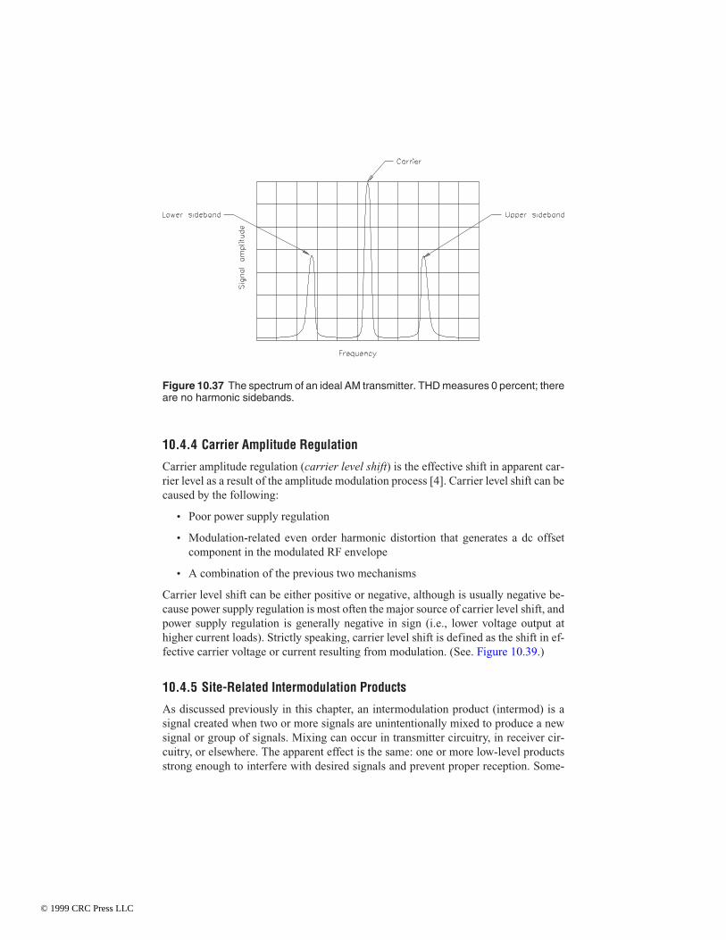
10.4.4 Carrier Amplitude Regulation
Carrier amplitude regulation (carrier level shift) is the effective shift in apparent car-rier level as a result of the amplitude modulation process [4]. Carrier level shift can becaused by the following:
• Poor power supply regulation
• Modulation-related even order harmonic distortion that generates a dc offsetcomponent in the modulated RF envelope
• A combination of the previous two mechanisms
Carrier level shift can be either positive or negative, although is usually negative be-cause power supply regulation is most often the major source of carrier level shift, andpower supply regulation is generally negative in sign (i.e., lower voltage output athigher current loads). Strictly speaking, carrier level shift is defined as the shift in ef-fective carrier voltage or current resulting from modulation. (See. Figure 10.39.)
10.4.5 Site-Related Intermodulation Products
As discussed previously in this chapter, an intermodulation product (intermod) is asignal created when two or more signals are unintentionally mixed to produce a newsignal or group of signals. Mixing can occur in transmitter circuitry, in receiver cir-cuitry, or elsewhere. The apparent effect is the same: one or more low-level productsstrong enough to interfere with desired signals and prevent proper reception. Some-
Figure 10.37 The spectrum of an ideal AM transmitter. THD measures 0 percent; thereare no harmonic sidebands.
© 1999 CRC Press LLC

times the intermod falls on unused frequencies. Sometimes it falls on a channel in useor near enough to the channel to cause interference.
It is possible to calculate the intermod that may result from frequencies in use at agiven transmission site. Normally produced by a computerized analysis, this intermodstudy is helpful in several ways. If the study is conducted as one or more new frequen-cies are under consideration for future use at an existing site, it may reveal which fre-quencies are more likely to produce a harmful intermod and which are not. If the studyis conducted as part of an investigation into an interference problem, it may help inidentifying transmitters that play a role in generating the intermod.
Intermod can be generated by any nonlinear device or circuit. The most commonplace for intermod to be generated is in the power amplifier of an FM transmitter. Suchan amplifier does not need to preserve waveform integrity; the waveform is restored bythe tuned output circuit. Thus, the amplifier is operated in an efficient but nonlinearmode, class C. In contrast, many amplifiers for AM service operate in a linear mode.Such amplifiers normally do not act as mixers.
Generally, solid-state amplifiers are better mixers than their electron tube counter-parts, a fact that may explain why intermod may appear suddenly when older equip-ment is replaced. A mix occurs when RF energy from one transmitter (Tx 1) finds itsway down the transmission line and into the final amplifier of another transmitter (Tx2), as illustrated in Figure 10.40. The energy mixes in the final amplifier with theprefiltered second harmonic of Tx 2 to produce another in-band signal, a third-orderintermod product. The reverse mix also may occur in the final amplifier of Tx 1, pro-ducing another intermod signal.
After the cause is discovered, a mix generated in a transmitter final amplifier is rela-tively easy to eliminate: Increase the isolation between the offending transmitters. This
Figure 10.38 The spectrum of an ideal transmitter with the addition of IPM.
© 1999 CRC Press LLC

may be accomplished by increasing the space between the antennas, or by placing anisolator at the output of each transmitter.
Receiver Intermod
Intermod also may be generated in the front end of a receiver. High-level RF energyfrom transmitters at a site can generate a bias voltage in the receiver sufficient toplace the receiver RF amplifier into a nonlinear state. In such a mode, the stage acts asa mixer and creates unwanted frequencies. Filters may be used to solve this problem.The filters should notch out the offending transmitted signals. If another transmitter isadded to the site, another notch filter usually must be added to the receiver transmis-sion line.
Hardware Intermod
At a large transmission site, the entire area—including towers, guy wires, antennas,clamps, and obstruction lighting hardware—is saturated by high-level RF. Any looseor moving hardware can cause broadband noise. Corroded connections, tower joints,or clamps can form semiconductor junctions that may generate harmful intermod.Because the antenna system is exposed to a changing external environment, the de-
Figure 10.39 Carrier amplitude regulation (carrier level shift) defined. (From [4]. Usedwith permission.)
© 1999 CRC Press LLC

gree of semiconductivity can vary with moisture or temperature. Changingsemiconductivity causes intermittent problems, at changing levels of severity.
10.5 References1. Hulick, Timothy P., “Very Simple Out-of-Band IMD Correctors for Adjacent Chan-
nel NTSC/DTV Transmitters,” Digital Television ‘98, Intertec Publishing, Over-land Park, KS, 1998.
2. Laboratory Staff, Care and Feeding of Power Grid Tubes, Varian/Eimac, SanCarlos, CA, 1984.
3. Mendenhall, Geoffrey N., M. Shrestha, and E. Anthony, “FM Broadcast Transmit-ters,” NAB Engineering Handbook, 8th Ed., E. B. Crutchfield (ed.), National Asso-ciation of Broadcasters, Washington, DC, pp. 463 - 464, 1992.
4. George Woodard, “AM Transmitters,” in NAB Engineering Handbook, 9th Ed.,Jerry C. Whitaker (ed.), National Association of Broadcasters, Washington, DC,1998.
10.6 BibliographyBenson, K. B., and Jerry C. Whitaker, Television and Audio Handbook for Engineers
and Technicians, McGraw-Hill, New York, 1989.Bordonaro, Dominic, “Reducing IPM in AM Transmitters,” Broadcast Engineering,
Intertec Publishing, Overland Park, KS, May 1988.Crutchfield, E. B. (ed.), NAB Engineering Handbook, 8th Ed., National Association of
Broadcasters, Washington, DC, 1992.
Figure 10.40 The mechanics of intermod generation at a two-transmitter installation.
© 1999 CRC Press LLC

Dolgosh, Al, and Ron Jakubowski, “Controlling Interference at CommunicationsSites,” Mobile Radio Technology, Intertec Publishing, Overland Park, KS, Febru-ary 1990.
Hershberger, David, and Robert Weirather, “Amplitude Bandwidth, Phase Bandwidth,Incidental AM, and Saturation Characteristics of Power Tube Cavity Amplifiers forFM,” application note, Harris Corporation, Quincy, IL, 1982.
Kinley, Harold, “Base Station Feedline Performance Testing,” Mobile Radio Technol-ogy, Intertec Publishing, Overland Park, KS, April 1989.
Mendenhall, Geoffrey N., “A Study of RF Intermodulation Between FM BroadcastTransmitters Sharing Filterplexed or Co-located Antenna Systems,” BroadcastElectronics, Quincy, IL, 1983.
Mendenhall, Geoffrey N., “A Systems Approach to Improving Subcarrier Perfor-mance,” Proceedings of the 1986 NAB Engineering Conference, National Associa-tion of Broadcasters, Washington, DC, 1986.
Mendenhall, Geoffrey N., “Fine Tuning FM Final Stages,” Broadcast Engineering,Intertec Publishing, Overland Park, KS, May 1987.
Mendenhall, Geoffrey N., “Improving FM Modulation Performance by Tuning forSymmetrical Group Delay,” Broadcast Electronics, Quincy IL, 1991.
Mendenhall, Geoffrey N., “Techniques for Measuring Synchronous AM Noise in FMTransmitters,” Broadcast Electronics, Quincy IL, 1988.
Mendenhall, Geoffrey N., “Testing Television Transmission Systems for Multichan-nel Sound Compatibility,” Broadcast Electronics, Quincy, IL, 1985.
Terman, F. E., Radio Engineering, 3rd Ed., McGraw-Hill, New York, 1947.Whitaker, Jerry C., Maintaining Electronic Systems, CRC Press, Boca Raton, FL,
1992.Whitaker, Jerry C., Radio Frequency Transmission Systems: Design and Operation,
McGraw-Hill, New York, 1990.Witte, Robert A., “Distortion Measurements Using a Spectrum Analyzer,” RF Design,
Cardiff Publishing, Denver, CO, pp. 75 - 84, September 1992.
© 1999 CRC Press LLC

Whitaker, Jerry C. “Chapter 11 – Safe Handling of Vacuum Tube Devices” Power Vacuum Tubes Handbook 2nd Edition.Ed. Jerry C. WhitakerBoca Raton: CRC Press LLC, 2000
© 1999 CRC Press LLC

Chapter
11Safe Handling of Vacuum Tube
Devices
11.1 IntroductionElectrical safety is important when working with any type of electronic hardware. Be-cause vacuum tubes operate at high voltages and currents, safety is doubly important.The primary areas of concern, from a safety standpoint, include:
• Electric shock
• Nonionizing radiation
• Beryllium oxide (BeO) ceramic dust
• Hot surfaces of vacuum tube devices
• Polychlorinated biphenyls (PCBs)
11.2 Electric ShockSurprisingly little current is required to injure a person. Studies at Underwriters Labo-ratories (UL) show that the electrical resistance of the human body varies with theamount of moisture on the skin, the muscular structure of the body, and the appliedvoltage. The typical hand-to-hand resistance ranges between 500 Ω and 600 kΩ, de-pending on the conditions. Higher voltages have the capability to break down theouter layers of the skin, which can reduce the overall resistance value. UL uses thelower value, 500 Ω, as the standard resistance between major extremities, such asfrom the hand to the foot. This value is generally considered the minimum that wouldbe encountered and, in fact, may not be unusual because wet conditions or a cut orother break in the skin significantly reduces human body resistance.
© 1999 CRC Press LLC

11.2.1 Effects on the Human Body
Table 11.1 lists some effects that typically result when a person is connected across acurrent source with a hand-to-hand resistance of 2.4 kΩ. The table shows that a cur-rent of approximately 50 mA will flow between the hands, if one hand is in contactwith a 120 V ac source and the other hand is grounded. The table indicates that eventhe relatively small current of 50 mA can produce ventricular fibrillation of the heart,and perhaps death. Medical literature describes ventricular fibrillation as rapid, unco-ordinated contractions of the ventricles of the heart, resulting in loss of synchroniza-tion between heartbeat and pulse beat. The electrocardiograms shown in Figure 11.1compare a healthy heart rhythm with one in ventricular fibrillation. Unfortunately,once ventricular fibrillation occurs, it will continue. Barring resuscitation techniques,death will ensue within a few minutes.
The route taken by the current through the body has a significant effect on the degreeof injury. Even a small current, passing from one extremity through the heart to anotherextremity, is dangerous and capable of causing severe injury or electrocution. There arecases where a person has contacted extremely high current levels and lived to tell aboutit. However, usually when this happens, the current passes only through a single limband not through the body. In these instances, the limb is often lost, but the person sur-vives.
Current is not the only factor in electrocution. Figure 11.2 summarizes the relation-ship between current and time on the human body. The graph shows that 100 mA flow-ing through a human adult body for 2 s will cause death by electrocution. An importantfactor in electrocution, the let-go range, also is shown on the graph. This range is de-scribed as the amount of current that causes “freezing”, or the inability to let go of theconductor. At 10 mA, 2.5 percent of the population will be unable to let go of a “live”conductor. At 15 mA, 50 percent of the population will be unable to let go of an ener-gized conductor. It is apparent from the graph that even a small amount of current can
Table 11.1 The Effects of Current on the Human Body
Current Effect1 mA or less No sensation, not feltMore than 3 mA Painful shockMore than 10 mA Local muscle contractions, sufficient to cause “freez-
ing” to the circuit for 2.5 percent of the populationMore than 15 mA Local muscle contractions, sufficient to cause “freez-
ing” to the circuit for 50 percent of the populationMore than 30 mA Breathing is difficult, can cause unconsciousness50 mA to 100 mA Possible ventricular fibrillation100 mA to 200 mA Certain ventricular fibrillationMore than 200 mA Severe burns and muscular contractions; heart more
apt to stop than to go into fibrillationMore than a few amperes Irreparable damage to body tissue
© 1999 CRC Press LLC

“freeze” someone to a conductor. The objective for those who must work around elec-tric equipment is how to protect themselves from electric shock. Table 11.2 lists re-quired precautions for personnel working around high voltages.
11.2.2 Circuit Protection Hardware
The typical primary panel or equipment circuit breaker or fuse will not protect a per-son from electrocution. In the time it takes a fuse or circuit breaker to blow, someonecould die. However, there are protection devices that, properly used, may help preventelectrocution. The ground-fault current interrupter (GFCI), shown in Figure 11.3,works by monitoring the current being applied to the load. The GFI uses a differentialtransformer and looks for an imbalance in load current. If a current (5 mA, ±1 mA)begins to flow between the neutral and ground or between the hot and ground leads,the differential transformer detects the leakage and opens up the primary circuitwithin 2.5 ms.
GFIs will not protect a person from every type of electrocution. If the victim be-comes connected to both the neutral and the hot wire, the GFI will not detect an imbal-ance.
11.2.3 Working with High Voltage
Rubber gloves are commonly used by engineers working on high-voltage equipment.These gloves are designed to provide protection from hazardous voltages or RF when
Figure 11.1 Electrocardiogram of a human heartbeat: (a) healthy rhythm, (b) ventricu-lar fibrillation.
(a)
(b)
© 1999 CRC Press LLC

the wearer is working on “hot” ac or RF circuits. Although the gloves may providesome protection from these hazards, placing too much reliance on them can have di-sastrous consequences. There are several reasons why gloves should be used with agreat deal of caution and respect. A common mistake made by engineers is to assumethat the gloves always provide complete protection. The gloves found in many facili-ties may be old or untested. Some may show signs of user repair, perhaps with electri-cal tape. Few tools could be more hazardous than such a pair of gloves.
Another mistake is not knowing the voltage rating of the gloves. Gloves are rated dif-ferently for both ac and dc voltages. For example, a class 0 glove has a minimum dcbreakdown voltage of 35 kV; the minimum ac breakdown voltage, however, is only 6kV. Furthermore, high-voltage rubber gloves are not usually tested at RF frequencies,
Figure 11.2 Effects of electric current and time on the human body. Note the “let-go”range.
© 1999 CRC Press LLC

and RF can burn a hole in the best of them. It is possible to develop dangerous workinghabits by assuming that gloves will offer the required protection.
Gloves alone may not be enough to protect an individual in certain situations. Recallthe axiom of keeping one hand in a pocket while working around a device with currentflowing? That advice is actually based on simple electricity. It is not the “hot” connec-tion that causes the problem, but the ground connection that lets the current begin toflow. Studies have shown that more than 90 percent of electric equipment fatalities oc-curred when the grounded person contacted a live conductor. Line-to-line electrocutionaccounted for less than 10 percent of the deaths.
When working around high voltages, always look for grounded surfaces. Keephands, feet, and other parts of the body away from any grounded surface. Even concrete
Table 11.2 Required Safety Practices for Engineers Working Around High-VoltageEquipment
High-Voltage Precautions Remove all ac power from the equipment. Do not rely on internal contactors or
SCRs to remove dangerous ac. Trip the appropriate power distribution circuit breakers at the main breaker
panel. Place signs as needed to indicate that the circuit is being serviced. Switch the equipment being serviced to the local control mode as provided. Discharge all capacitors using the discharge stick provided by the manufac-
turer. Do not remove, short circuit, or tamper with interlock switches on access cov-
ers, doors, enclosures, gates, panels, or shields. Keep away from live circuits.
Figure 11.3 Basic design of a ground-fault interrupter (GFI).
© 1999 CRC Press LLC

can act as a ground if the voltage is sufficiently high. If work must be performed in“live” cabinets, then consider using, in addition to rubber gloves, a rubber floor mat,rubber vest, and rubber sleeves. Although this may seem to be a lot of trouble, considerthe consequences of making a mistake. Of course, the best troubleshooting methodol-ogy is never to work on any circuit without being certain that no hazardous voltages arepresent. In addition, any circuits or contactors that normally contain hazardous volt-ages should be firmly grounded before work begins.
RF Considerations
Engineers often rely on electrical gloves when making adjustments to live RF circuits.This practice, however, can be extremely dangerous. Consider the typical load match-ing unit shown in Figure 11.4. In this configuration, disconnecting the coil from eitherL2 or L3 places the full RF output literally at the engineer’s fingertips. Depending onthe impedances involved, the voltages can become quite high, even in a circuit thatnormally is relatively tame.
In the Figure 11.4 example, assume that the load impedance is approximately 106+j202 Ω. With 1 kW feeding into the load, the rms voltage at the matching output will beapproximately 700 V. The peak voltage (which determines insulating requirements)will be close to 1 kV, and perhaps more than twice that if the carrier is being ampli-tude-modulated. At the instant the output coil clip is disconnected, the current in theshunt leg will increase rapidly, and the voltage easily could more than double.
11.2.4 First Aid Procedures
All engineers working around high-voltage equipment should be familiar with firstaid treatment for electric shock and burns. Always keep a first aid kit on hand at thefacility. Figure 11.5 illustrates the basic treatment for victims of electric shock. Copy
Figure 11.4 Example of how high voltages can be generated in an RF load matchingunit.
© 1999 CRC Press LLC

Figure 11.5 Basic first aid treatment for electric shock.
© 1999 CRC Press LLC

the information, and post it in a prominent location. Better yet, obtain more detailedinformation from the local heart association or Red Cross chapter. Personalized in-struction on first aid usually is available locally.
11.3 Operating HazardsA number of potential hazards exist in the operation and maintenance of high-powervacuum tube RF equipment. Maintenance personnel must exercise extreme carearound such hardware. Consider the following guidelines:
• Use caution around the high-voltage stages of the equipment. Many power tubesoperate at voltages high enough to kill through electrocution. Always break theprimary ac circuit of the power supply, and discharge all high-voltage capacitors.
• Minimize exposure to RF radiation. Do not permit personnel to be in the vicinityof open, energized RF generating circuits, RF transmission systems(waveguides, cables, or connectors), or energized antennas. High levels of radia-tion can result in severe bodily injury, including blindness. Cardiac pacemakersmay also be affected.
• Avoid contact with beryllium oxide (BeO) ceramic dust and fumes. BeO ceramicmaterial may be used as a thermal link to carry heat from a tube to the heat sink.Do not perform any operation on any BeO ceramic that might produce dust orfumes, such as grinding, grit blasting, or acid cleaning. Beryllium oxide dust andfumes are highly toxic, and breathing them can result in serious injury or death.BeO ceramics must be disposed of as prescribed by the device manufacturer.
• Avoid contact with hot surfaces within the equipment. The anode portion of mostpower tubes is air-cooled. The external surface normally operates at a high tem-perature (up to 250°C). Other portions of the tube also may reach high tempera-tures, especially the cathode insulator and the cathode/heater surfaces. All hotsurfaces may remain hot for an extended time after the tube is shut off. To preventserious burns, avoid bodily contact with these surfaces during tube operation andfor a reasonable cool-down period afterward. Table 11.3 lists basic first aid pro-cedures for burns.
11.3.1 OSHA Safety Considerations
The U.S. government has taken a number of steps to help improve safety within theworkplace under the auspices of the Occupational Safety and Health Administration(OSHA). The agency helps industries monitor and correct safety practices. OSHAhas developed a number of guidelines designed to help prevent accidents. OSHA re-cords show that electrical standards are among the most frequently violated of allsafety standards. Table 11.4 lists 16 of the most common electrical violations, includ-ing exposure of live conductors, improperly labeled equipment, and faulty grounding.
© 1999 CRC Press LLC

Protective Covers
Exposure of live conductors is a common safety violation. All potentially dangerouselectric conductors should be covered with protective panels. The danger is thatsomeone may come into contact with the exposed current-carrying conductors. It isalso possible for metallic objects such as ladders, cable, or tools to contact a hazard-ous voltage, creating a life-threatening condition. Open panels also present a fire haz-ard.
Identification and Marking
Circuit breakers and switch panels should be properly identified and labeled. Labelson breakers and equipment switches may be many years old and may no longer reflectthe equipment actually in use. This is a safety hazard. Casualties or unnecessary dam-age can be the result of an improperly labeled circuit panel if no one who understandsthe system is available in an emergency. If a number of devices are connected to a sin-gle disconnect switch or breaker, a diagram should be provided for clarification. La-bel with brief phrases, and use clear, permanent, and legible markings.
Equipment marking is a closely related area of concern. This is not the same thing asequipment identification. Marking equipment means labeling the equipment breaker
Table 11.3 Basic First Aid Procedures for Burns (More detailed information can be ob-tained from any Red Cross office.)
Extensively Burned and Broken Skin Cover affected area with a clean sheet or cloth. Do not break blisters, remove tissue, remove adhered particles of clothing, or
apply any salve or ointment. Treat victim for shock as required. Arrange for transportation to a hospital as quickly as possible. If arms or legs are affected, keep them elevated. If medical help will not be available within an hour and the victim is conscious
and not vomiting, prepare a weak solution of salt and soda: 1 level teaspoon ofsalt and 1
2 level teaspoon of baking soda to each quart of tepid water. Allow thevictim to sip slowly about 4 ounces (half a glass) over a period of 15 minutes.Discontinue fluid intake if vomiting occurs. (Do not offer alcohol.)
Less Severe Burns (First and Second Degree) Apply cool (not ice-cold) compresses using the cleanest available cloth article. Do not break blisters, remove tissue, remove adhered particles of clothing, or
apply salve or ointment. Apply clean, dry dressing if necessary. Treat victim for shock as required. Arrange for transportation to a hospital as quickly as possible. If arms or legs are affected, keep them elevated.
© 1999 CRC Press LLC

panels and ac disconnect switches according to device rating. Breaker boxes shouldcontain a nameplate showing the manufacturer, rating, and other pertinent electricalfactors. The intent is to prevent devices from being subjected to excessive loads or volt-ages.
Grounding
OSHA regulations describe two types of grounding: system grounding and equipmentgrounding. System grounding actually connects one of the current-carrying conduc-tors (such as the terminals of a supply transformer) to ground. (See Figure 11.6.)Equipment grounding connects all of the noncurrent-carrying metal surfaces togetherand to ground. From a grounding standpoint, the only difference between a groundedelectrical system and an ungrounded electrical system is that the main bondingjumper from the service equipment ground to a current-carrying conductor is omittedin the ungrounded system. The system ground performs two tasks:
• It provides the final connection from equipment-grounding conductors to thegrounded circuit conductor, thus completing the ground-fault loop.
Table 11.4 Sixteen Common OSHA Violations (After [1].)
Fact Sheet Subject NEC1 Reference1 Guarding of live parts 110-172 Identification 110-223 Uses allowed for flexible cord 400-74 Prohibited uses of flexible cord 400-85 Pull at joints and terminals must be prevented 400-106.1 Effective grounding, Part 1 250-516.2 Effective grounding, Part 2 250-517 Grounding of fixed equipment, general 250-428 Grounding of fixed equipment, specific 250-439 Grounding of equipment connected by cord
and plug250-45
10 Methods of grounding, cord andplug-connected equipment
250-59
11 AC circuits and systems to be grounded 250-512 Location of overcurrent devices 240-2413 Splices in flexible cords 400-914 Electrical connections 110-1415 Marking equipment 110-2116 Working clearances about electric equipment 110-16
1 National Electrical Code
© 1999 CRC Press LLC

• It solidly ties the electrical system and its enclosures to their surroundings (usu-ally earth, structural steel, and plumbing). This prevents voltages at any sourcefrom rising to harmfully high voltage-to-ground levels.
Figure 11.6 AC service entrance bonding requirements: (a) 120 V phase-to-neutral(240 V phase-to-phase), (b) 3-phase 208 V wye (120 V phase-to-neutral), (c) 3-phase240 V (or 480 V) delta. Note that the main bonding jumper is required in only two of thedesigns.
(a)
(b)
(c)
© 1999 CRC Press LLC

Note that equipment grounding—bonding all electric equipment to ground—is re-quired whether or not the system is grounded. Equipment grounding serves two im-portant tasks:
• It bonds all surfaces together so that there can be no voltage difference amongthem.
• It provides a ground-fault current path from a fault location back to the electricalsource, so that if a fault current develops, it will rise to a level high enough to op-erate the breaker or fuse.
The National Electrical Code (NEC) is complex and contains numerous require-ments concerning electrical safety. The fact sheets listed in Table 11.4 are availablefrom OSHA.
11.3.2 Beryllium Oxide Ceramics
Some tubes, both power grid and microwave, contain beryllium oxide (BeO) ceram-ics, typically at the output waveguide window or around the cathode. Never performany operations on BeO ceramics that produce dust or fumes, such as grinding, gritblasting, or acid cleaning. Beryllium oxide dust and fumes are highly toxic, andbreathing them can result in serious personal injury or death.
If a broken window is suspected on a microwave tube, carefully remove the devicefrom its waveguide, and seal the output flange of the tube with tape. Because BeOwarning labels may be obliterated or missing, maintenance personnel should contactthe tube manufacturer before performing any work on the device. Some tubes haveBeO internal to the vacuum envelope.
Take precautions to protect personnel working in the disposal or salvage of tubescontaining BeO. All such personnel should be made aware of the deadly hazards in-volved and the necessity for great care and attention to safety precautions. Some tubemanufacturers will dispose of tubes without charge, provided they are returned to themanufacturer prepaid, with a written request for disposal.
11.3.3 Corrosive and Poisonous Compounds
The external output waveguides and cathode high-voltage bushings of microwavetubes are sometimes operated in systems that use a dielectric gas to impede micro-wave or high-voltage breakdown. If breakdown does occur, the gas may decomposeand combine with impurities, such as air or water vapor, to form highly toxic and cor-rosive compounds. Examples include Freon gas, which may form lethal phosgene,and sulfur hexafluoride (SF6) gas, which may form highly toxic and corrosive sulfuror fluorine compounds such as beryllium fluoride. When breakdown does occur in thepresence of these gases, proceed as follows:
• Ventilate the area to outside air
• Avoid breathing any fumes or touching any liquids that develop
© 1999 CRC Press LLC

• Take precautions appropriate for beryllium compounds and for other highly toxicand corrosive substances
If a coolant other than pure water is used, follow the precautions supplied by the cool-ant manufacturer.
11.3.4 FC-75 Toxic Vapor
The decomposition products of FC-75 are highly toxic. Decomposition may occur asa result of any of the following:
• Exposure to temperatures above 200°C
• Exposure to liquid fluorine or alkali metals (lithium, potassium, or sodium)
• Exposure to ionizing radiation
Known thermal decomposition products include perfluoroisobutylene (PFIB; [CF3]2
C = CF2), which is highly toxic in small concentrations.If FC-75 has been exposed to temperatures above 200°C through fire, electric heat-
ing, or prolonged electric arcs, or has been exposed to alkali metals or strong ionizingradiation, take the following steps:
• Strictly avoid breathing any fumes or vapors.
• Thoroughly ventilate the area.
• Strictly avoid any contact with the FC-75.
Under such conditions, promptly replace the FC-75 and handle and dispose of thecontaminated FC-75 as a toxic waste.
11.3.5 Nonionizing Radiation
Nonionizing radio frequency radiation (RFR) resulting from high-intensity RF fieldsis a growing concern to engineers who must work around high-power transmissionequipment. The principal medical concern regarding nonionizing radiation involvesheating of various body tissues, which can have serious effects, particularly if there isno mechanism for heat removal. Recent research has also noted, in some cases, subtlepsychological and physiological changes at radiation levels below the threshold forheat-induced biological effects. However, the consensus is that most effects are ther-mal in nature.
High levels of RFR can affect one or more body systems or organs. Areas identifiedas potentially sensitive include the ocular (eye) system, reproductive system, and theimmune system. Nonionizing radiation also is thought to be responsible for metaboliceffects on the central nervous system and cardiac system.
In spite of these studies, many of which are ongoing, there is still no clear evidencein Western literature that exposure to medium-level nonionizing radiation results indetrimental effects. Russian findings, on the other hand, suggest that occupational ex-
© 1999 CRC Press LLC

posure to RFR at power densities above 1.0 mW/cm2 does result in symptoms, particu-larly in the central nervous system.
Clearly, the jury is still out as to the ultimate biological effects of RFR. Until the situ-ation is better defined, however, the assumption must be made that potentially seriouseffects can result from excessive exposure. Compliance with existing standards shouldbe the minimum goal, to protect members of the public as well as facility employees.
NEPA Mandate
The National Environmental Policy Act of 1969 required the Federal Communica-tions Commission to place controls on nonionizing radiation. The purpose was to pre-vent possible harm to the public at large and to those who must work near sources ofthe radiation. Action was delayed because no hard and fast evidence existed that low-and medium-level RF energy is harmful to human life. Also, there was no evidenceshowing that radio waves from radio and TV stations did not constitute a health haz-ard.
During the delay, many studies were carried out in an attempt to identify those levelsof radiation that might be harmful. From the research, suggested limits were developedby the American National Standards Institute (ANSI) and stated in the documentknown as ANSI C95.1-1982. The protection criteria outlined in the standard are shownin Figure 11.7.
The energy-level criteria were developed by representatives from a number of in-dustries and educational institutions after performing research on the possible effectsof nonionizing radiation. The projects focused on absorption of RF energy by the hu-man body, based upon simulated human body models. In preparing the document,ANSI attempted to determine those levels of incident radiation that would cause the
Figure 11.7 The power density limits for nonionizing radiation exposure for humans.
© 1999 CRC Press LLC

body to absorb less than 0.4 W/kg of mass (averaged over the whole body) or peak ab-sorption values of 8 W/kg over any 1 gram of body tissue.
From the data, the researchers found that energy would be absorbed more readily atsome frequencies than at others. The absorption rates were found to be functions of thesize of a specific individual and the frequency of the signal being evaluated. It was theresult of these absorption rates that culminated in the shape of the safe curve shown inthe figure. ANSI concluded that no harm would come to individuals exposed to radioenergy fields, as long as specific values were not exceeded when averaged over a periodof 0.1 hour. It was also concluded that higher values for a brief period would not posedifficulties if the levels shown in the standard document were not exceeded when aver-aged over the 0.1-hour time period.
The FCC adopted ANSI C95.1-1982 as a standard that would ensure adequate pro-tection to the public and to industry personnel who are involved in working around RFequipment and antenna structures.
Revised Guidelines
The ANSI C95.1-1982 standard was intended to be reviewed at 5-year intervals. Ac-cordingly, the 1982 standard was due for reaffirmation or revision in 1987. The pro-cess was indeed begun by ANSI, but was handed off to the Institute of Electrical andElectronics Engineers (IEEE) for completion. In 1991, the revised document wascompleted and submitted to ANSI for acceptance as ANSI/IEEE C95.1-1992.
The IEEE standard incorporated changes from the 1982 ANSI document in fourmajor areas:
• An additional safety factor was provided in certain situations. The most signifi-cant change was the introduction of new uncontrolled (public) exposure guide-lines, generally established at one-fifth of the controlled (occupational) exposureguidelines. Figure 11.8 illustrates the concept for the microwave frequency band.
• For the first time, guidelines were included for body currents; examination of theelectric and magnetic fields were determined to be insufficient to determine com-pliance.
• Minor adjustments were made to occupational guidelines, including relaxation ofthe guidelines at certain frequencies and the introduction of breakpoints at newfrequencies.
• Measurement procedures were changed in several aspects, most notably with re-spect to spatial averaging and to minimum separation from reradiating objectsand structures at the site.
The revised guidelines are complex and beyond the scope of this handbook. Refer tothe ANSI/IEEE document for details.
© 1999 CRC Press LLC

Multiple-User Sites
At a multiple-user site, the responsibility for assessing the RFR situation—althoughofficially triggered by either a new user or the license renewal of all site tenants—is,in reality, the joint responsibility of all the site tenants. In a multiple-user environmentinvolving various frequencies, and various protection criteria, compliance is indicatedwhen the fraction of the RFR limit within each pertinent frequency band is estab-lished and added to the sum of all the other fractional contributions. The sum must notbe greater than 1.0. Evaluating the multiple-user environment is not a simple matter,and corrective actions, if indicated, may be quite complex.
Operator Safety Considerations
RF energy must be contained properly by shielding and transmission lines. All inputand output RF connections, cables, flanges, and gaskets must be RF leakproof. Thefollowing guidelines should be followed at all times:
• Never operate a power tube without a properly matched RF energy absorbingload attached.
• Never look into or expose any part of the body to an antenna or open RF generat-ing tube, circuit, or RF transmission system that is energized.
• Monitor the RF system for radiation leakage at regular intervals and after servic-ing.
Figure 11.8 ANSI/IEEE exposure guidelines for microwave frequencies.
© 1999 CRC Press LLC

11.3.6 X-Ray Radiation Hazard
The voltages typically used in microwave tubes are capable of producing dangerous Xrays. As voltages increase beyond 15 kV, metal-body tubes are capable of producingprogressively more dangerous radiation. Adequate X-ray shielding must be providedon all sides of such tubes, particularly at the cathode and collector ends, as well as atthe modulator and pulse transformer tanks (as appropriate). High-voltage tubes nevershould be operated without adequate X-ray shielding in place. The X-ray radiation ofthe device should be checked at regular intervals and after servicing.
11.3.7 Implosion Hazard
Because of the high internal vacuum in power grid and microwave tubes, the glass orceramic output window or envelope can shatter inward (implode) if struck with suffi-cient force or exposed to sufficient mechanical shock. Flying debris could result inbodily injury, including cuts and puncture wounds. If the device is made of berylliumoxide ceramic, implosion may produce highly toxic dust or fumes.
In the event of such an implosion, assume that toxic BeO ceramic is involved unlessconfirmed otherwise.
11.3.8 Hot Coolant and Surfaces
Extreme heat occurs in the electron collector of a microwave tube and the anode of apower grid tube during operation. Coolant channels used for water or vapor coolingalso can reach high temperatures (boiling—100°C—and above), and the coolant istypically under pressure (as high as 100 psi). Some devices are cooled by boiling thecoolant to form steam.
Contact with hot portions of the tube or its cooling system can scald or burn. Care-fully check that all fittings and connections are secure, and monitor back pressure forchanges in cooling system performance. If back pressure is increased above normal op-erating values, shut the system down and clear the restriction.
For a device whose anode or collector is air-cooled, the external surface normallyoperates at a temperature of 200 to 300°C. Other parts of the tube also may reach hightemperatures, particularly the cathode insulator and the cathode/heater surfaces. Allhot surfaces remain hot for an extended time after the tube is shut off. To prevent seriousburns, take care to avoid bodily contact with these surfaces during operation and for areasonable cool-down period afterward.
11.3.9 Polychlorinated Biphenyls
PCBs belong to a family of organic compounds known as chlorinated hydrocarbons.Virtually all PCBs in existence today have been synthetically manufactured. PCBshave a heavy oil-like consistency, high boiling point, a high degree of chemical stabil-ity, low flammability, and low electrical conductivity. These characteristics resulted inthe widespread use of PCBs in high-voltage capacitors and transformers. Commercial
© 1999 CRC Press LLC

products containing PCBs were widely distributed between 1957 and 1977 under sev-eral trade names including:
• Aroclor
• Pyroclor
• Sanotherm
• Pyranol
• Askarel
Askarel is also a generic name used for nonflammable dielectric fluids containingPCBs. Table 11.5 lists some common trade names used for Askarel. These tradenames typically will be listed on the nameplate of a PCB transformer or capacitor.
PCBs are harmful because once they are released into the environment, they tend notto break apart into other substances. Instead, PCBs persist, taking several decades toslowly decompose. By remaining in the environment, they can be taken up and stored inthe fatty tissues of all organisms, from which they are slowly released into the blood-stream. Therefore, because of the storage in fat, the concentration of PCBs in body tis-sues can increase with time, even though PCB exposure levels may be quite low. Thisprocess is called bioaccumulation. Furthermore, as PCBs accumulate in the tissues ofsimple organisms, and as they are consumed by progressively higher organisms, theconcentration increases. This process is called biomagnification. These two factors areespecially significant because PCBs are harmful even at low levels. Specifically, PCBshave been shown to cause chronic (long-term) toxic effects in some species of animalsand aquatic life. Well-documented tests on laboratory animals show that various levelsof PCBs can cause reproductive effects, gastric disorders, skin lesions, and canceroustumors.
PCBs may enter the body through the lungs, the gastrointestinal tract, and the skin.After absorption, PCBs are circulated in the blood throughout the body and stored in
PCB Trade Names
Apirolio Abestol Askarel1 Aroclor B Chlorexto ChlophenChlorinol Clorphon Diaclor DK Dykanol EEC-18Elemex Eucarel Fenclor Hyvol Inclor InerteenKanechlor No-Flamol Phenodlor Pydraul Pyralene PyranolPyroclor Sal-T-Kuhl Santothern FR Santovac Solvol Thermin
1 Generic name used for nonflammable dielectric fluids containing PCBs.
Table 11.5 Commonly Used Names for PCB Insulating Material
© 1999 CRC Press LLC

fatty tissues and a variety of organs, including the liver, kidneys, lungs, adrenal glands,brain, heart, and skin.
The health risk from PCBs lies not only in the PCB itself, but also in the chemicalsthat develop when PCBs are heated. Laboratory studies have confirmed that PCBby-products, including polychlorinated dibenzofurans (PCDFs) and polychlorinateddibenzo-p-dioxins (PCDDs), are formed when PCBs or chlorobenzenes are heated totemperatures ranging from approximately 900 to 1300°F. Unfortunately, these prod-ucts are more toxic than PCBs themselves.
Governmental Action
The U.S. Congress took action to control PCBs in October 1975 by passing the ToxicSubstances Control Act (TSCA). A section of this law specifically directed the EPAto regulate PCBs. Three years later the Environmental Protection Agency (EPA) is-sued regulations to implement the congressional ban on the manufacture, processing,distribution, and disposal of PCBs. Since that time, several revisions and updates havebeen issued by the EPA. One of these revisions, issued in 1982, specifically addressedthe type of equipment used in industrial plants and transmitting stations. Failure toproperly follow the rules regarding the use and disposal of PCBs has resulted in highfines and even jail sentences.
Although PCBs are no longer being produced for electrical products in the UnitedStates, there are thousands of PCB transformers and millions of small PCB capacitorsstill in use or in storage. The threat of widespread contamination from PCB fire-relatedincidents is one reason behind the EPA’s efforts to reduce the number of PCB productsin the environment. The users of high-power equipment are affected by the regulationsprimarily because of the widespread use of PCB transformers and capacitors. Thesecomponents usually are located in older (pre-1979) systems, so this is the first place tolook for them. However, some facilities also maintain their own primary power trans-formers. Unless these transformers are of recent vintage, it is quite likely that they toocontain a PCB dielectric. Table 11.6 lists the primary classifications of PCB devices.
PCB Components
The two most common PCB components are transformers and capacitors. A PCBtransformer is one containing at least 500 ppm (parts per million) PCBs in the dielec-tric fluid. An Askarel transformer generally has 600,000 ppm or more. A PCB trans-former may be converted to a PCB-contaminated device (50 to 500 ppm) or anon-PCB device (less than 50 ppm) by having it drained, refilled, and tested. The test-ing must not take place until the transformer has been in service for a minimum of 90days. Note that this is not something a maintenance technician can do. It is the exclu-sive domain of specialized remanufacturing companies.
PCB transformers must be inspected quarterly for leaks. If an impervious dike isbuilt around the transformer sufficient to contain all of the liquid material, the inspec-tions can be conducted yearly. Similarly, if the transformer is tested and found to con-
© 1999 CRC Press LLC

Table 11.6 Definition of PCB Terms as Identified by the EPA
Term Definition ExamplesPCB Any chemical substance that
is limited to the biphenyl mole-cule that has been chlorinatedto varying degrees, or anycombination of substancesthat contain such substances.
PCB dielectric fluids, PCBheat-transfer fluids, PCBhydraulic fluids,2,2’,4-trichlorobiphenyl
PCB article Any manufactured article,other than a PCB container,that contains PCBs andwhose surface has been indirect contact with PCBs.
Capacitors, transformers,electric motors, pumps,pipes
PCB container A device used to containPCBs or PCB articles, andwhose surface has been indirect contact with PCBs.
Packages, cans, bottles,bags, barrels, drums,tanks
PCB article container A device used to contain PCBarticles or equipment, andwhose surface has not been indirect contact with PCBs.
Packages, cans, bottles,bags, barrels, drums,tanks
PCB equipment Any manufactured item, otherthan a PCB container or PCBarticle container, that containsa PCB article or other PCBequipment.
Microwave systems,fluorescent light ballasts,electronic equipment
PCB item Any PCB article, PCB articlecontainer, PCB container, orPCB equipment thatdeliberately or unintentionallycontains, or has as a part of it,any PCBs.
PCB transformer Any transformer that containsPCBs in concentrations of 500ppm or greater.
PCB contaminated Any electric equipment thatcontains more than 50, butless than 500 ppm of PCBs.(Oil-filled electric equipmentother than circuit breakers,reclosers, and cable whosePCB concentration is un-known must be assumed to bePCB-contaminated electricequipment.)
Transformers, capacitors,contaminated circuit break-ers, reclosers, voltage reg-ulators, switches, cable,electromagnets
© 1999 CRC Press LLC

tain less than 60,000 ppm, a yearly inspection is sufficient. Failed PCB transformerscannot be repaired; they must be properly disposed of.
If a leak develops, it must be contained and daily inspections begun. A cleanup mustbe initiated as soon as possible, but no later than 48 hours after the leak is discovered.Adequate records must be kept of all inspections, leaks, and actions taken for 3 years af-ter disposal of the component. Combustible materials must be kept a minimum of 5 mfrom a PCB transformer and its enclosure.
As of October 1, 1990, the use of PCB transformers (500 ppm or greater) was pro-hibited in or near commercial buildings when the secondary voltages are 480 V ac orhigher.
The EPA regulations also require that the operator notify others of the possible dan-gers. All PCB transformers (including PCB transformers in storage for reuse) must beregistered with the local fire department. The following information must be supplied:
• The location of the PCB transformer(s).
• Address(es) of the building(s) and, for outdoor PCB transformers, the location.
• Principal constituent of the dielectric fluid in the transformer(s).
• Name and telephone number of the contact person in the event of a fire involvingthe equipment.
Any PCB transformers used in a commercial building must be registered with thebuilding owner. All building owners within 30 m of such PCB transformers also mustbe notified. In the event of a fire-related incident involving the release of PCBs, theCoast Guard National Spill Response Center (800-424-8802) must be notified imme-diately. Appropriate measures also must be taken to contain and control any possiblePCB release into water.
Capacitors are divided into two size classes, large and small. A PCB small capacitorcontains less than 1.36 kg (3 lbs) of dielectric fluid. A capacitor having less than 100 in3
also is considered to contain less than 3 lb of dielectric fluid. A PCB large capacitor hasa volume of more than 200 in3 and is considered to contain more than 3 lb of dielectricfluid. Any capacitor having a volume between 100 and 200 in3 is considered to contain3 lb of dielectric, provided the total weight is less than 9 lb. A PCB large high-voltagecapacitor contains 3 lb or more of dielectric fluid and operates at voltages of 2 kV orgreater. A large low-voltage capacitor also contains 3 lb or more of dielectric fluid butoperates below 2 kV.
The use and servicing of PCB small capacitors is not restricted by the EPA unlessthere is a leak. In that event, the leak must be repaired or the capacitor disposed of. Dis-posal may be handled by an approved incineration facility, or the component may beplaced in a specified container and buried in an approved chemical waste landfill. Itemssuch as capacitors that are leaking oil greater than 500 ppm PCBs should be taken to anEPA-approved PCB disposal facility.
© 1999 CRC Press LLC

PCB Liability Management
Properly managing the PCB risk is not particularly difficult; the keys are understand-ing the regulations and following them carefully. Any program should include the fol-lowing steps:
• Locate and identify all PCB devices. Check all stored or spare devices.
• Properly label PCB transformers and capacitors according to EPA requirements.
• Perform the required inspections and maintain an accurate log of PCB items, theirlocation, inspection results, and actions taken. These records must be maintainedfor 3 years after disposal of the PCB component.
• Complete the annual report of PCBs and PCB items by July 1 of each year. Thisreport must be retained for 5 years.
• Arrange for necessary disposal through a company licensed to handle PCBs. Ifthere are any doubts about the company’s license, contact the EPA.
• Report the location of all PCB transformers to the local fire department and to theowners of any nearby buildings.
The importance of following the EPA regulations cannot be overstated.
11.4 References1. National Electrical Code, NFPA #70.
11.5 Bibliography“Current Intelligence Bulletin #45,” National Institute for Occupational Safety and
Health, Division of Standards Development and Technology Transfer, February 24,1986.
Code of Federal Regulations, 40, Part 761.“Electrical Standards Reference Manual,” U.S. Department of Labor, Washington,
DC.Hammett, William F., “Meeting IEEE C95.1-1991 Requirements,” NAB 1993 Broad-
cast Engineering Conference Proceedings, National Association of Broadcasters,Washington, D.C., pp. 471 - 476, April 1993.
Hammar, Willie, Occupational Safety Management and Engineering, Prentice Hall,New York.
Markley, Donald, “Complying with RF Emission Standards,” Broadcast Engineering,Intertec Publishing, Overland Park, KS, May 1986.
“Occupational Injuries and Illnesses in the United States by Industry,” OSHA Bulletin2278, U.S. Department of Labor, Washington, DC, 1985.
OSHA, “Electrical Hazard Fact Sheets,” U.S. Department of Labor, Washington, DC,January 1987.
OSHA, “Handbook for Small Business,” U.S. Department of Labor, Washington, DC.
© 1999 CRC Press LLC

Pfrimmer, Jack, “Identifying and Managing PCBs in Broadcast Facilities,” 1987 NABEngineering Conference Proceedings, National Association of Broadcasters,Washington, DC, 1987.
“Safety Precautions,” Publication no. 3386A, Varian Associates, Palo Alto, CA,March 1985.
Smith, Milford K., Jr., “RF Radiation Compliance,” Proceedings of the Broadcast En-gineering Conference, Society of Broadcast Engineers, Indianapolis, IN, 1989.
“Toxics Information Series,” Office of Toxic Substances, July 1983.Whitaker, Jerry C., AC Power Systems, 2nd Ed., CRC Press, Boca Raton, FL, 1998.Whitaker, Jerry C., G. DeSantis, and C. Paulson, Interconnecting Electronic Systems,
CRC Press, Boca Raton, FL, 1993.Whitaker, Jerry C., Maintaining Electronic Systems, CRC Press, Boca Raton, FL,
1991.Whitaker, Jerry C., Radio Frequency Transmission Systems: Design and Operation,
McGraw-Hill, New York, 1990.
© 1999 CRC Press LLC

Whitaker, Jerry C. “Chapter 12 – Reference Data” Power Vacuum Tubes Handbook 2nd Edition.Ed. Jerry C. WhitakerBoca Raton: CRC Press LLC, 2000
© 1999 CRC Press LLC

Chapter
12Reference Data
Standard Units
Name Symbol Quantity
ampere A electric currentampere per meter A/m magnetic field strengthampere per square meter A/m2 current densityBecquerel Bq activity (of a radionuclide)candela cd luminous intensitycoulomb C electric chargecoulomb per kilogram C/kg exposure (x- and gamma-rays)coulomb per sq. meter C/m2 electric flux densitycubic meter m3 volumecubic meter per kilogram m3/kg specific volumedegree Celsius °C Celsius temperaturefarad F capacitancefarad per meter F/m permittivityhenry H inductancehenry per meter H/m permeabilityhertz Hz frequencyjoule J energy, work, quantity of heatjoule per cubic meter J/m3 energy densityjoule per kelvin J/K heat capacityjoule per kilogram K J/(kg-K) specific heat capacityjoule per mole J/mol molar energykelvin K thermodynamic temperaturekilogram kg masskilogram per cubic meter kg/m3 density, mass densitylumen lm luminous fluxlux lx luminancemeter m lengthmeter per second m/s speed, velocitymeter per second sq. m/s2 acceleration(Continued on next page)
© 1999 CRC Press LLC

Name Symbol Quantity
mole mol amount of substancepascal Pa pressure, stresspascal second Pa•s dynamic viscosityradian rad plane angleradian per second rad/s angular velocityradian per second squared rad/s2 angular accelerationsecond s timesiemens S electric conductancesquare meter m2 areasteradian sr solid angletesla T magnetic flux densityvolt V electrical potentialvolt per meter V/m electric field strengthwatt W power, radiant fluxwatt per meter kelvin W/(m•K) thermal conductivitywatt per square meter W/m2 heat (power) flux densityweber Wb magnetic flux
Standard Units Continued
Standard Prefixes
Multiple Prefix Symbol
1018 exa E1015 peta P1012 tera T109 giga G106 mega M103 kilo k102 hecto h10 deka da10-1 deci d10-2 centi c10-3 milli m10-6 micro µ10-9 nano n10-12 pico p10-15 femto f10-18 atto a
© 1999 CRC Press LLC

Common Standard Units for Electronics Work
Unit Symbol
centimeter cmcubic centimeter cm3
cubic meter per second m3/sgigahertz GHzgram gkilohertz kHzkilohm kΩkilojoule kJkilometer kmkilovolt kVkilovoltampere kVAkilowatt kWmegahertz MHzmegavolt MVmegawatt MWmegohm MΩmicroampere µAmicrofarad µFmicrogram µgmicrohenry µHmicrosecond µsmicrowatt µWmilliampere mAmilligram mgmillihenry mHmillimeter mmmillisecond msmillivolt mVmilliwatt mWnanoampere nAnanofarad nFnanometer nmnanosecond nsnanowatt nWpicoampere pApicofarad pFpicosecond pspicowatt pW
© 1999 CRC Press LLC

Power Conversion Factors (Decibels to Watts)
dBm dBw Watts Multiple Prefix
+150 +120 1,000,000,000,000 1012 1 terawatt+140 +110 100,000,000,000 1011 100 gigawatts+130 +100 10,000,000,000 1010 10 gigawatts+120 +90 1,000,000,000 109 1 gigawatt+110 +80 100,000,000 108 100 megawatts+100 +70 10,000,000 107 10 megawatts+90 +60 1,000,000 106 1 megawatt+80 +50 100,000 105 100 kilowatts+70 +40 10,000 104 10 kilowatts+60 +30 1000 103 1 kilowatt+50 +20 100 102 1 hectowatt+40 +10 10 10 1 decawatt+30 0 1 1 1 watt+20 –10 0.1 10–1 1 deciwatt+10 –20 0.01 10–2 1 centiwatt0 –30 0.001 10–3 1 milliwatt–10 –40 0.0001 10–4 100 microwatts–20 –50 0.00001 10–5 10 microwatts–30 –60 0.000,001 10–6 1 microwatt–40 –70 0.0,000,001 10–7 100 nanowatts–50 –80 0.00,000,001 10–8 10 nanowatts–60 –90 0.000,000,001 10–9 1 nanowatt–70 –100 0.0,000,000,001 10–10 100 picowatts–80 –110 0.00,000,000,001 10–11 10 picowatts–90 –120 0.000,000,000,001 10–12 1 picowatt
© 1999 CRC Press LLC

VSWR Reflection Return Power PercentCoefficient Loss Ratio Reflected
1.01:1 0.0050 46.1 dB 0.00002 0.0021.02:1 0.0099 40.1 dB 0.00010 0.0101.04:1 0.0196 34.2 dB 0.00038 0.0381.06:1 0.0291 30.7 dB 0.00085 0.0851.08:1 0.0385 28.3 dB 0.00148 0.1481.10:1 0.0476 26.4 dB 0.00227 0.2271.20:1 0.0909 20.8 dB 0.00826 0.8261.30:1 0.1304 17.7 dB 0.01701 1.71.40:1 0.1667 15.6 dB 0.02778 2.81.50:1 0.2000 14.0 dB 0.04000 4.01.60:1 0.2308 12.7 dB 0.05325 5.31.70:1 0.2593 11.7 dB 0.06722 6.71.80:1 0.2857 10.9 dB 0.08163 8.21.90:1 0.3103 10.2 dB 0.09631 9.62.00:1 0.3333 9.5 dB 0.11111 11.12.20:1 0.3750 8.5 dB 0.14063 14.12.40:1 0.4118 7.7 dB 0.16955 17.02.60:1 0.4444 7.0 dB 0.19753 19.82.80:1 0.4737 6.5 dB 0.22438 22.43.00:1 0.5000 6.0 dB 0.25000 25.03.50:1 0.5556 5.1 dB 0.30864 30.94.00:1 0.6000 4.4 dB 0.36000 36.04.50:1 0.6364 3.9 dB 0.40496 40.55.00:1 0.6667 3.5 dB 0.44444 44.46.00:1 0.7143 2.9 dB 0.51020 51.07.00:1 0.7500 2.5 dB 0.56250 56.38.00:1 0.7778 2.2 dB 0.60494 60.59.00:1 0.8000 1.9 dB 0.64000 64.010.00:1 0.8182 1.7 dB 0.66942 66.915.00:1 0.8750 1.2 dB 0.76563 76.620.00:1 0.9048 0.9 dB 0.81859 81.930.00:1 0.9355 0.6 dB 0.87513 97.540.00:1 0.9512 0.4 dB 0.90482 90.550.00:1 0.9608 0.3 dB 0.92311 92.3
Voltage Standing Wave Ratio and Key Parameters
© 1999 CRC Press LLC

Wire Diam. Circular Turns Per Linear Inch1 Ohms Current- Diam.Size in mil Per Carrying inAWG mils Area enam. SCE DCC 100 ft2 Capacity3 mm
1 289.3 83810 - - - 0.1239 119.6 7.3482 257.6 05370 - - - 0.1563 94.8 6.5443 229.4 62640 - - - 0.1970 75.2 5.8274 204.3 41740 - - - 0.2485 59.6 5.1895 181.9 33100 - - - 0.3133 47.3 4.6216 162.0 26250 - - - 0.3951 37.5 4.1157 144.3 20820 - - - 0.4982 29.7 3.6658 128.5 16510 7.6 - 7.1 0.6282 23.6 3.2649 114.4 13090 8.6 - 7.8 0.7921 18.7 2.90610 101.9 10380 9.6 9.1 8.9 0.9989 14.8 2.58811 90.7 8234 10.7 - 9.8 1.26 11.8 2.30512 80.8 6530 12.0 11.3 10.9 1.588 9.33 2.06313 72.0 5178 13.5 - 12.8 2.003 7.40 1.82814 64.1 4107 15.0 14.0 13.8 2.525 5.87 1.62815 57.1 3257 16.8 - 14.7 3.184 4.65 1.45016 50.8 2583 18.9 17.3 16.4 4.016 3.69 1.29117 45.3 2048 21.2 - 18.1 5.064 2.93 1.15018 40.3 1624 23.6 21.2 19.8 6.386 2.32 1.02419 35.9 1288 26.4 - 21.8 8.051 1.84 0.91220 32.0 1022 29.4 25.8 23.8 10.15 1.46 0.81221 28.5 810 33.1 - 26.0 12.8 1.16 0.72322 25.3 642 37.0 31.3 30.0 16.14 0.918 0.64423 22.6 510 41.3 - 37.6 20.36 0.728 0.57324 20.1 404 46.3 37.6 35.6 25.67 0.577 0.51125 17.9 320 51.7 - 38.6 32.37 0.458 0.45526 15.9 254 58.0 46.1 41.8 40.81 0.363 0.40627 14.2 202 64.9 - 45.0 51.47 0.288 0.36128 12.6 160 72.7 54.6 48.5 64.9 0.228 0.32129 11.3 127 81.6 - 51.8 81.83 0.181 0.28630 10.0 101 90.5 64.1 55.5 103.2 0.144 0.25531 8.9 50 101 - 59.2 130.1 0.114 0.22732 8.0 63 113 74.1 61.6 164.1 0.090 0.20233 7.1 50 127 - 66.3 206.9 0.072 0.18034 6.3 40 143 86.2 70.0 260.9 0.057 0.16035 5.6 32 158 - 73.5 329.0 0.045 0.14336 5.0 25 175 103.1 77.0 414.8 0.036 0.12737 4.5 20 198 - 80.3 523.1 0.028 0.11338 4.0 16 224 116.3 83.6 659.6 0.022 0.10139 3.5 12 248 - 86.6 831.8 0.018 0.0901. Based on 25.4 mm.2. Ohms per 1000 ft measured at 20°C.3. Current-carrying capacity at 700 circular mils per amp.
Specifications of Standard Copper Wire
© 1999 CRC Press LLC

°Celsius °Fahrenheit °Celsius °Fahrenheit
–50 –58 125 257–45 –49 130 266–40 –40 135 275–35 –31 140 284–30 –22 145 293–25 –13 150 302–20 4 155 311–15 5 160 320–10 14 165 329–5 23 170 3380 32 175 3475 41 180 35610 50 185 36515 59 190 37420 68 195 38325 77 200 39230 86 205 40135 95 210 41040 104 215 41945 113 220 42850 122 225 43755 131 230 44660 140 235 45565 149 240 46470 158 245 47375 167 250 48280 176 255 49185 185 260 50090 194 265 50995 203 270 518100 212 275 527105 221 280 536110 230 285 545115 239 290 554120 248 295 563
Celsius-to-Fahrenheit Conversion
© 1999 CRC Press LLC

Inch 0 1/8 1/4 3/8 1/2 5/8 3/4 7/8 Inch
0 0.0 3.18 6.35 9.52 12.70 15.88 19.05 22.22 01 25.40 28.58 31.75 34.92 38.10 41.28 44.45 47.62 12 50.80 53.98 57.15 60.32 63.50 66.68 69.85 73.02 23 76.20 79.38 82.55 85.72 88.90 92.08 95.25 98.42 34 101.6 104.8 108.0 111.1 114.3 117.5 120.6 123.8 45 127.0 130.2 133.4 136.5 139.7 142.9 146.0 149.2 56 152.4 155.6 158.8 161.9 165.1 168.3 171.4 174.6 67 177.8 181.0 184.2 187.3 190.5 193.7 196.8 200.0 78 203.2 206.4 209.6 212.7 215.9 219.1 222.2 225.4 89 228.6 231.8 235.0 238.1 241.3 244.5 247.6 250.8 910 254.0 257.2 260.4 263.5 266.7 269.9 273.0 276.2 1011 279 283 286 289 292 295 298 302 1112 305 308 311 314 317 321 324 327 1213 330 333 337 340 343 346 349 352 1314 356 359 362 365 368 371 375 378 1415 381 384 387 391 394 397 400 403 1516 406 410 413 416 419 422 425 429 1617 432 435 438 441 445 448 451 454 1718 457 460 464 467 470 473 476 479 1819 483 486 489 492 495 498 502 505 1920 508 511 514 518 521 524 527 530 20
Inch-to-Millimeter Conversion
© 1999 CRC Press LLC

mm Inches mm Inches mm Inches
1 0.039370 46 1.811020 91 3.5826702 0.078740 47 1.850390 92 3.6220403 0.118110 48 1.889760 93 3.6614104 0.157480 49 1.929130 94 3.7007805 0.196850 50 1.968500 95 3.7401506 0.236220 51 2.007870 96 3.7795207 0.275590 52 2.047240 97 3.8188908 0.314960 53 2.086610 98 3.8582609 0.354330 54 2.125980 99 3.89763010 0.393700 55 2.165350 100 3.93700011 0.433070 56 2.204720 105 4.13384812 0.472440 57 2.244090 110 4.33070013 0.511810 58 2.283460 115 4.52755014 0.551180 59 2.322830 120 4.72440015 0.590550 60 2.362200 125 4.92125016 0.629920 61 2.401570 210 8.26770017 0.669290 62 2.440940 220 8.66140018 0.708660 63 2.480310 230 9.05510019 0.748030 64 2.519680 240 9.44880020 0.787400 65 2.559050 250 9.84250021 0.826770 66 2.598420 260 10.23620022 0.866140 67 2.637790 270 10.62990023 0.905510 68 2.677160 280 11.03260024 0.944880 69 2.716530 290 11.41730025 0.984250 70 2.755900 300 11.81100026 1.023620 71 2.795270 310 12.20470027 1.062990 72 2.834640 320 12.59840028 1.102360 73 2.874010 330 12.99210029 1.141730 74 2.913380 340 13.38580030 1.181100 75 2.952750 350 13.77950031 1.220470 76 2.992120 360 14.17320032 1.259840 77 3.031490 370 14.56690033 1.299210 78 3.070860 380 14.96060034 1.338580 79 3.110230 390 15.35430035 1.377949 80 3.149600 400 15.74800036 1.417319 81 3.188970 500 19.68500037 1.456689 82 3.228340 600 23.62200038 1.496050 83 3.267710 700 27.55900039 1.535430 84 3.307080 800 31.49600040 1.574800 85 3.346450 900 35.43300041 1.614170 86 3.385820 1000 39.37000042 1.653540 87 3.425190 2000 78.74000043 1.692910 88 3.464560 3000 118.11000044 1.732280 89 3.503903 4000 157.48000045 1.771650 90 3.543300 5000 196.850000
Millimeters-to-Decimal Inches Conversion
© 1999 CRC Press LLC
Common Decimal mm Common Decimal mmFractions1 Fractions1 (approx.) Fractions Fractions (appox.)
1/128 0.008 0.20 1/2 0.500 12.701/64 0.016 0.40 33/64 0.516 13.101/32 0.031 0.79 17/32 0.531 13.493/64 0.047 1.19 35/64 0.547 13.891/16 0.063 1.59 9/16 0.563 14.295/64 0.078 1.98 37/64 0.578 14.683/32 0.094 2.38 19/32 0.594 15.087/64 0.109 2.78 39/64 0.609 15.481/8 0.125 3.18 5/8 0.625 15.889/64 0.141 3.57 41/64 0.641 16.275/32 0.156 3.97 21/32 0.656 16.6711/64 0.172 4.37 43/64 0.672 17.073/16 0.188 4.76 11/16 0.688 17.4613/64 0.203 5.16 45/64 0.703 17.867/32 0.219 5.56 23/32 0.719 18.2615/64 0.234 5.95 47/64 0.734 18.651/4 0.250 6.35 3/4 0.750 19.0517/64 0.266 6.75 49/64 0.766 19.459/32 0.281 7.14 25/32 0.781 19.8419/64 0.297 7.54 51/64 0.797 20.245/16 0.313 7.94 13/16 0.813 20.6421/64 0.328 8.33 53/64 0.828 21.0311/32 0.344 8.73 27/32 0.844 21.4323/64 0.359 9.13 55/64 0.859 21.833/8 0.375 9.53 7/8 0.875 22.2325/64 0.391 9.92 57/64 0.891 22.6213/32 0.406 10.32 29/32 0.906 23.0227/64 0.422 10.72 59/64 0.922 23.427/16 0.438 11.11 15/16 0.938 23.8129/64 0.453 11.51 61/64 0.953 24.2115/32 0.469 11.91 31/32 0.969 24.6131/64 0.484 12.30 63/64 0.984 25.00
1 Units in inches.
Conversion of Common Fractions to Decimal and Millimeter Units
© 1999 CRC Press LLC

Known Quantity Multiply By Quantity to Find
inches (in) 2.54 centimeters (cm)feet (ft) 30 centimeters (cm)yards (yd) 0.9 meters (m)miles (mi) 1.6 kilometers (km)millimeters (mm) 0.04 inches (in)centimeters (cm) 0.4 inches (in)meters (m) 3.3 feet (ft)meters (m) 1.1 yards (yd)kilometers (km) 0.6 miles (mi)centimeters (cm) 10 millimeters (mm)decimeters (dm) 10 centimeters (cm)decimeters (dm) 100 millimeters (mm)meters (m) 10 decimeters (dm)meters (m) 1000 millimeters (mm)dekameters (dam) 10 meters (m)hectometers (hm) 10 dekameters (dam)hectometers (hm) 100 meters (m)kilometers (km) 10 hectometers (hm)kilometers (km) 1000 meters (m)
Conversion Ratios for Length
Known Quantity Multiply By Quantity to Find
square inches (in2) 6.5 square centimeters (cm2)square feet (ft2) 0.09 square meters (m2)square yards (yd2) 0.8 square meters (m2)square miles (mi2) 2.6 square kilometers (km2)acres 0.4 hectares (ha)square centimeters (cm2) 0.16 square inches (in2)square meters (m2) 1.2 square yards (yd2)square kilometers (km2) 0.4 square miles (mi2)hectares (ha) 2.5 acressquare centimeters (cm2) 100 square millimeters (mm2)square meters (m2) 10,000 square centimeters (cm2)square meters (m2) 1,000,000 square millimeters (mm2)ares (a) 100 square meters (m2)hectares (ha) 100 ares (a)hectares (ha) 10,000 square meters (m2)square kilometers (km2) 100 hectares (ha)square kilometers (km2) 1,000 square meters (m2)
Conversion Ratios for Area
© 1999 CRC Press LLC

Known Quantity Multiply By Quantity to Find
ounces (oz) 28 grams (g)pounds (lb) 0.45 kilograms (kg)tons 0.9 tonnes (t)grams (g) 0.035 ounces (oz)kilograms (kg) 2.2 pounds (lb)tonnes (t) 100 kilograms (kg)tonnes (t) 1.1 tonscentigrams (cg) 10 milligrams (mg)decigrams (dg) 10 centigrams (cg)decigrams (dg) 100 milligrams (mg)grams (g) 10 decigrams (dg)grams (g) 1000 milligrams (mg)dekagram (dag) 10 grams (g)hectogram (hg) 10 dekagrams (dag)hectogram (hg) 100 grams (g)kilograms (kg) 10 hectograms (hg)kilograms (kg) 1000 grams (g)metric tons (t) 1000 kilograms (kg)
Conversion Ratios for Mass
Known Quantity Multiply By Quantity to Find
milliliters (mL) 0.03 fluid ounces (fl oz)liters (L) 2.1 pints (pt)liters (L) 1.06 quarts (qt)liters (L) 0.26 gallons (gal)gallons (gal) 3.8 liters (L)quarts (qt) 0.95 liters (L)pints (pt) 0.47 liters (L)cups (c) 0.24 liters (L)fluid ounces (fl oz) 30 milliliters (mL)teaspoons (tsp) 5 milliliters (mL)tablespoons (tbsp) 15 milliliters (mL)liters (L) 100 milliliters (mL)
Conversion Ratios for Volume
© 1999 CRC Press LLC

Known Quantity Multiply By Quantity to Find
cubic meters (m3) 35 cubic feet (ft3)cubic meters (m3) 1.3 cubic yards (yd3)cubic yards (yd3) 0.76 cubic meters (m3)cubic feet (ft3) 0.028 cubic meters (m3)cubic centimeters (cm3) 1000 cubic millimeters (mm3)cubic decimeters (dm3) 1000 cubic centimeters (cm3)cubic decimeters (dm3) 1,000,000 cubic millimeters (mm3)cubic meters (m3) 1000 cubic decimeters (dm3)cubic meters (m3) 1 sterescubic feet (ft3) 1728 cubic inches (in3)cubic feet (ft3) 28.32 liters (L)cubic inches (in3) 16.39 cubic centimeters (cm3)cubic meters (m3) 264 gallons (gal)cubic yards (yd3) 27 cubic feet (ft3)cubic yards (yd3) 202 gallons (gal)gallons (gal) 231 cubic inches (in3)
Conversion Ratios for Cubic Measure
Known Quantity Multiply By Quantity to Find
Btu per minute 0.024 horsepower (hp)Btu per minute 17.57 watts (W)horsepower (hp) 33,000 foot-pounds per min (ft-lb/min)horsepower (hp) 746 watts (W)kilowatts (kW) 57 Btu per minutekilowatts (kW) 1.34 horsepower (hp)
Conversion Ratios for Electrical Quantities
© 1999 CRC Press LLC

Basic Electrical Units
Unit Symbol DefinitionAmpere A One ampere is the constant current flowing in two parallel
conductors one meter apart that would produce a force of2× 10–7 newtons per meter of length.
Coulomb C One coulomb is the charge that is moved in one second by acurrent of one ampere.
Farad F One farad is the capacitance of a capacitor that produces apotential of one volt between the plates when charged to onecoulomb.
Henry H One henry is the inductance of a coil that has one volt in-duced in it when the current varies uniformly at one ampereper second.
Joule J One joule is the work done by a force of one newton actingover a distance of one meter.
Ohm Ω One ohm is the resistance between two points of a conductorthat produces a current of one ampere when one volt is ap-plied between these points.
Siemens S One siemens is the conductance between two points of aconductor that produces a current of one ampere when onevolt is applied between these points. Reciprocal of the ohm.(Formerly mho).
Volt V One volt is the potential difference between two points in awire carrying one ampere when the power dissipated be-tween these points is one watt.
Watt W One watt is the power that produces energy at one joule persecond.
Weber Wb One weber is the magnetic flux that produces an electromo-tive force of one volt in a circuit of one turn as the fluxchanges uniformly from maximum to zero in one second.
© 1999 CRC Press LLC

Whitaker, Jerry C. “Chapter 13 – Glossary” Power Vacuum Tubes Handbook 2nd Edition.Ed. Jerry C. WhitakerBoca Raton: CRC Press LLC, 2000

Chapter
13Glossary
Aab so lute de lay The amount of time a sig nal is de layed. The de lay may be ex pressed in
time or num ber of pulse events.ab so lute zero The low est tem per a ture the o ret i cally pos si ble, –273.16°C. Ab so lute
zero is equal to zero de grees Kel vin.ab sorp tion The trans fer ence of some or all of the en ergy con tained in an elec tro mag -
netic wave to the sub stance or me dium in which it is prop a gat ing or upon which it isin ci dent.
ab sorp tion auroral The loss of en ergy in a ra dio wave pass ing through an area af -fected by so lar auroral ac tiv ity.
ac cou pling A method of cou pling one cir cuit to an other through a ca pac i tor or trans -former so as to trans mit the vary ing (ac) char ac ter is tics of the sig nal while block ingthe static (dc) char ac ter is tics.
ac/dc cou pling Cou pling be tween cir cuits that ac com mo dates the pass ing of both acand dc sig nals (may also be re ferred to as sim ply dc cou pling).
ac cel er ated life test A spe cial form of re li abil ity test ing per formed by an equip mentman u fac turer. The unit un der test is sub jected to stresses that ex ceed those typ i callyex pe ri enced in nor mal op er a tion. The goal of an ac cel er ated life test is to im provethe re li abil ity of prod ucts shipped by forc ing la tent fail ures in com po nents to be -come ev i dent be fore the unit leaves the fac tory.
ac cel er at ing elec trode The elec trode that causes elec trons emit ted from an elec trongun to ac cel er ate in their jour ney to the screen of a cath ode ray tube.
ac cel er at ing volt age The volt age ap plied to an elec trode that ac cel er ates a beam ofelec trons or other charged par ti cles.
ac cept able re li abil ity level The max i mum num ber of fail ures al lowed per thou sandop er at ing hours of a given com po nent or sys tem.
ac cep tance test The pro cess of test ing newly pur chased equip ment to en sure that it isfully com pli ant with con trac tual spec i fi ca tions.
ac cess The point at which en try is gained to a cir cuit or fa cil ity.ac qui si tion time In a com mu ni ca tion sys tem, the amount of time re quired to at tain
syn chro nism.ac tive Any de vice or cir cuit that in tro duces gain or uses a source of en ergy other than
that in her ent in the sig nal to per form its func tion.

adapter A fit ting or elec tri cal con nec tor that links equip ment that can not be con necteddi rectly.
adap tive A de vice able to ad just or re act to a con di tion or ap pli ca tion, as an adap tivecir cuit. This term usu ally re fers to fil ter cir cuits.
adap tive sys tem A gen eral name for a sys tem that is ca pa ble of reconfiguring it self tomeet new re quire ments.
ad der A de vice whose out put rep re sents the sum of its in puts.ad ja cent chan nel in ter fer ence In ter fer ence to com mu ni ca tions caused by a trans mit -
ter op er at ing on an ad ja cent ra dio chan nel. The side bands of the trans mit ter mixwith the car rier be ing re ceived on the de sired chan nel, re sult ing in noise.
ad mit tance A mea sure of how well al ter nat ing cur rent flows in a con duc tor. It is the re -cip ro cal of im ped ance and is ex pressed in siemens. The real part of ad mit tance iscon duc tance; the imag i nary part is susceptance.
AFC (au to matic fre quency con trol) A cir cuit that au to mat i cally keeps an os cil la toron fre quency by com par ing the out put of the os cil la tor with a stan dard fre quencysource or sig nal.
air core An in duc tor with no mag netic ma te rial in its core.al go rithm A pre scribed fi nite set of well-defined rules or pro cesses for the so lu tion of a
prob lem in a fi nite num ber of steps.align ment The ad just ment of cir cuit com po nents so that an en tire sys tem meets min i -
mum per for mance val ues. For ex am ple, the stages in a ra dio are aligned to en sureproper re cep tion.
al lo ca tion The planned use of cer tain fa cil i ties and equip ment to meet cur rent, pend -ing, and/or fore casted cir cuit- and car rier-system re quire ments.
al ter nat ing cur rent (ac) A con tin u ously vari able cur rent, ris ing to a max i mum in onedi rec tion, fall ing to zero, then re vers ing di rec tion and ris ing to a max i mum in theother di rec tion, then fall ing to zero and re peat ing the cy cle. Al ter nating cur rent usu -ally fol lows a si nu soi dal growth and de cay curve. Note that the cor rect us age of theterm ac is lower case.
al ter na tor A gen er a tor that pro duces al ter nat ing cur rent elec tric power.am bi ent elec tro mag netic en vi ron ment The ra di ated or con ducted elec tro mag netic
sig nals and noise at a spe cific lo ca tion and time.am bi ent level The mag ni tude of ra di ated or con ducted elec tro mag netic sig nals and
noise at a spe cific test lo ca tion when equip ment-under-test is not pow ered.am bi ent tem per a ture The tem per a ture of the sur round ing me dium, typ i cally air, that
co mes into con tact with an ap pa ra tus. Am bi ent tem per a ture may also re fer sim ply to room tem per a ture.
Amer i can Na tional Stan dards In sti tute (ANSI) A non profit or ga ni za tion that co or -di nates vol un tary stan dards ac tiv i ties in the U.S.
Amer i can Wire Gauge (AWG) The stan dard Amer i can method of clas si fy ing wiredi am e ter.
am me ter An in stru ment that mea sures and re cords the amount of cur rent in am peresflow ing in a cir cuit.
amp (A) An ab bre vi a tion of the term am pere.ampacity A mea sure of the cur rent car ry ing ca pac ity of a power ca ble. Ampacity is de -
ter mined by the max i mum con tin u ous-performance tem per a ture of the in su la tion,by the heat gen er ated in the ca ble (as a re sult of con duc tor and in su la tion losses), and by the heat-dissipating prop er ties of the ca ble and its en vi ron ment.
am pere (amp) The stan dard unit of elec tric cur rent.

am pere per me ter The stan dard unit of mag netic field strength.am pere-hour The en ergy that is con sumed when a cur rent of one am pere flows for a
pe riod of one hour.am pere-turns The prod uct of the num ber of turns of a coil and the cur rent in am peres
flow ing through the coil.am pli fi ca tion The pro cess that re sults when the out put of a cir cuit is an en larged re pro -
duc tion of the in put sig nal. Am pli fiers may be de signed to pro vide am pli fi ca tion ofvolt age, cur rent, or power, or a com bi na tion of these quan ti ties.
am pli fi ca tion fac tor In a vac uum tube, the ra tio of the change in plate volt age to thechange in grid volt age that causes a cor re spond ing change in plate cur rent. Am pli fi -ca tion fac tor is ex pressed by the Greek let ter µ (mu).
am pli fier (1—gen eral) A de vice that re ceives an in put sig nal and pro vides as an out -put a mag ni fied rep lica of the in put wave form. (2—au dio) An am pli fier de signed tocover the nor mal au dio fre quency range (20 Hz to 20 kHz). (3—bal anced) A cir cuitwith two iden ti cal con nected sig nal branches that op er ate in phase op po si tion, within put and out put con nec tions each bal anced to ground. (4—bridg ing) An am pli fy -ing cir cuit fea tur ing high in put im ped ance to pre vent load ing of the source.(5—broad band) An am pli fier ca pa ble of op er at ing over a spec i fied broad band offre quen cies with ac cept ably small am pli tude vari a tions as a func tion of fre quency.(6—buffer) An am pli fier stage used to iso late a fre quency-sensitive cir cuit fromvari a tions in the load pre sented by fol low ing stages. (7—lin ear) An am pli fier inwhich the in stan ta neous out put sig nal is a lin ear func tion of the cor re spond ing in putsig nal. (8—mag netic) An am pli fier in cor po rat ing a con trol de vice de pend ent onmag netic sat u ra tion. A small dc sig nal ap plied to a con trol cir cuit trig gers a largechange in op er at ing im ped ance and, hence, in the out put of the cir cuit. (9—mi cro -phone) A cir cuit that am pli fies the low level out put from a mi cro phone to make itsuf fi cient to be used as an in put sig nal to a power am pli fier or an other stage in amod u la tion cir cuit. Such a cir cuit is com monly known as a preamplifier.(10—push-pull) A bal anced am pli fier with two sim i lar am pli fy ing units con nectedin phase op po si tion in or der to can cel un de sired har mon ics and min i mize dis tor tion. (11—tuned ra dio fre quency) An am pli fier tuned to a par tic u lar ra dio fre quency orband so that only se lected fre quen cies are am pli fied.
am pli fier op er at ing class (1—gen eral) The op er at ing point of an am pli fy ing stage.The op er at ing point, termed the op er at ing class, de ter mines the pe riod dur ing which cur rent flows in the out put. (2—class A) An am pli fier in which out put cur rent flowsdur ing the whole of the in put cur rent cy cle. (3—class AB) An am pli fier in which the out put cur rent flows for more than half but less than the whole of the in put cy cle.(4—class B) An am pli fier in which out put cur rent is cut off at zero in put sig nal; ahalf-wave rec ti fied out put is pro duced. (5—class C) An am pli fier in which out putcur rent flows for less than half the in put cy cle. (6—class D) An am pli fier op er at ingin a pulse-only mode.
am pli tude The mag ni tude of a sig nal in volt age or cur rent, fre quently ex pressed interms of peak, peak-to-peak, or root-mean-square (RMS). The ac tual am pli tude of a quan tity at a par tic u lar in stant of ten var ies in a si nu soi dal man ner.
am pli tude dis tor tion A dis tor tion mech a nism oc cur ring in an am pli fier or other de -vice when the out put am pli tude is not a lin ear func tion of the in put am pli tude un derspec i fied con di tions.
am pli tude equal izer A cor rec tive net work that is de signed to mod ify the am pli tudechar ac ter is tics of a cir cuit or sys tem over a de sired fre quency range.

am pli tude-versus-frequency dis tor tion The dis tor tion in a trans mis sion sys temcaused by the non uni form at ten u a tion or gain of the sys tem with re spect to fre -quency un der spec i fied con di tions.
an a log car rier sys tem A car rier sys tem whose sig nal am pli tude, fre quency, or phase is var ied con tin u ously as a func tion of a mod u lat ing in put.
an ode (1 — gen eral) A pos i tive pole or el e ment. (2—vac uum tube) The out er mostpos i tive el e ment in a vac uum tube, also called the plate . (3—bat tery) The pos i tiveel e ment of a bat tery or cell.
an od ize The for ma tion of a thin film of ox ide on a me tal lic sur face, usu ally to pro ducean in su lat ing layer.
an tenna (1—gen eral) A de vice used to trans mit or re ceive a ra dio sig nal. An an tennais usu ally de signed for a spec i fied fre quency range and serves to cou ple elec tro mag -netic en ergy from a trans mis sion line to and/or from the free space through which ittrav els. Di rec tional an ten nas con cen trate the en ergy in a par tic u lar hor i zon tal orver ti cal di rec tion. (2—aperiodic) An an tenna that is not pe ri odic or res o nant at par -tic u lar fre quen cies, and so can be used over a wide band of fre quen cies. (3—ar ti fi -cial) A de vice that be haves, so far as the trans mit ter is con cerned, like a proper an -tenna, but does not ra di ate any power at ra dio fre quen cies. (4—broad band) An an -tenna that op er ates within spec i fied per for mance lim its over a wide band of fre quen -cies, with out re quir ing re tun ing for each in di vid ual fre quency. (5—Cassegrain) Adou ble re flect ing an tenna, of ten used for ground sta tions in sat el lite sys tems.(6—co ax ial) A di pole an tenna made by fold ing back on it self a quar ter wave lengthof the outer con duc tor of a co ax ial line, leav ing a quar ter wave length of the in nercon duc tor ex posed. (7—cor ner) An an tenna within the an gle formed by twoplane-reflecting sur faces. (8—di pole) A cen ter-fed an tenna, one half-wavelengthlong. (9—di rec tional) An an tenna de signed to re ceive or emit ra di a tion more ef fi -ciently in a par tic u lar di rec tion. (10—dummy) An ar ti fi cial an tenna, de signed toac cept power from the trans mit ter but not to ra di ate it. (11—fer rite) A com mon AM broad cast re ceive an tenna that uses a small coil mounted on a short rod of fer rite ma -te rial. (12—flat top) An an tenna in which all the hor i zon tal com po nents are in thesame hor i zon tal plane. (13—folded di pole) A ra di at ing de vice con sist ing of two or -di nary half-wave di poles joined at their outer ends and fed at the cen ter of one of thedi poles. (14—horn re flec tor) A ra di a tor in which the feed horn ex tends into a par a -bolic re flec tor, and the power is ra di ated through a win dow in the horn. (15—iso tro -pic) A the o ret i cal an tenna in free space that trans mits or re ceives with the same ef fi -ciency in all di rec tions. (16—log-periodic) A broad band di rec tional an tenna in cor -po rat ing an ar ray of di poles of dif fer ent lengths, the length and spac ing be tween di -poles in creas ing logarithmically away from the feeder el e ment. (17—long wire) An an tenna made up of one or more con duc tors in a straight line point ing in the re quireddi rec tion with a to tal length of sev eral wave lengths at the op er at ing fre quency.(18—loop) An an tenna con sist ing of one or more turns of wire in the same or par al -lel planes. (19—nested rhombic) An as sem bly of two rhombic an ten nas, onesmaller than the other, so that the com plete di a mond-shaped an tenna fits in side thearea oc cu pied by the larger unit. (20—omnidirectional) An an tenna whose ra di at -ing or re ceiv ing prop er ties are the same in all hor i zon tal plane di rec tions. (21—pe -ri odic) A res o nant an tenna de signed for use at a par tic u lar fre quency. (22—quar -ter-wave) A di pole an tenna whose length is equal to one quar ter of a wave length atthe op er at ing fre quency. (23—rhombic) A large di a mond-shaped an tenna, withsides of the di a mond sev eral wave lengths long. The rhombic an tenna is fed at one of

the cor ners, with di rec tional ef fi ciency in the di rec tion of the di ag o nal. (24—se riesfed) A ver ti cal an tenna that is fed at its lower end. (25—shunt fed) A ver ti cal an -tenna whose base is grounded, and is fed at a spec i fied point above ground. Thepoint at which the an tenna is fed above ground de ter mines the op er at ing im ped ance.(26—steer able) An an tenna so con structed that its ma jor lobe may readily bechanged in di rec tion. (27—top-loaded) A ver ti cal an tenna ca pac i tively loaded at its up per end, of ten by sim ple en large ment or the at tach ment of a disc or plate.(28—turn stile) An an tenna with one or more tiers of hor i zon tal di poles, crossed atright an gles to each other and with ex ci ta tion of the di poles in phase quad ra ture.(29—whip) An an tenna con structed of a thin semiflexible metal rod or tube, fed atits base. (30—Yagi) A di rec tional an tenna con structed of a se ries of di poles cut tospe cific lengths. Di rec tor el e ments are placed in front of the ac tive di pole and re -flec tor el e ments are placed be hind the ac tive el e ment.
an tenna ar ray A group of sev eral an ten nas cou pled to gether to yield a re quired de greeof directivity.
an tenna beam width The an gle be tween the half-power points (3 dB points) of themain lobe of the an tenna pat tern when ref er enced to the peak power point of the an -tenna pat tern. An tenna beam width is mea sured in de grees and nor mally re fers to thehor i zon tal ra di a tion pat tern.
an tenna directivity fac tor The ra tio of the power flux den sity in the de sired di rec tionto the av er age value of power flux den sity at crests in the an tenna directivity pat ternin the in ter fer ence sec tion.
an tenna fac tor A fac tor that, when ap plied to the volt age ap pear ing at the ter mi nals ofmea sure ment equip ment, yields the elec tri cal field strength at an an tenna. The unitof an tenna fac tor is volts per me ter per mea sured volt.
an tenna gain The ra tio of the power re quired at the in put of a the o ret i cally per fectomnidirectional ref er ence an tenna to the power sup plied to the in put of the given an -tenna to pro duce the same field at the same dis tance. When not spec i fied oth er wise,the fig ure ex press ing the gain of an an tenna re fers to the gain in the di rec tion of thera di a tion main lobe. In ser vices us ing scat ter ing modes of prop a ga tion, the full gainof an an tenna may not be re al iz able in prac tice and the ap par ent gain may vary withtime.
an tenna gain-to-noise tem per a ture For a sat el lite earth ter mi nal re ceiv ing sys tem, afig ure of merit that equals G/T, where G is the gain in dB of the earth ter mi nal an -tenna at the re ceive fre quency, and T is the equiv a lent noise tem per a ture of the re -ceiv ing sys tem in Kel vins.
an tenna match ing The pro cess of ad just ing an an tenna match ing cir cuit (or the an -tenna it self) so that the in put im ped ance of the an tenna is equal to the char ac ter is ticim ped ance of the trans mis sion line.
an tenna mon i tor A de vice used to mea sure the ra tio and phase be tween the cur rentsflow ing in the tow ers of a di rec tional AM broad cast sta tion.
an tenna noise tem per a ture The tem per a ture of a re sis tor hav ing an avail able noisepower per unit band width equal to that at the an tenna out put at a spec i fied fre -quency.
an tenna pat tern A di a gram show ing the ef fi ciency of ra di a tion in all di rec tions fromthe an tenna.
an tenna power rat ing The max i mum con tin u ous-wave power that can be ap plied toan an tenna with out de grad ing its per for mance.

an tenna preamplifier A small am pli fier, usu ally mast-mounted, for am pli fy ing weaksig nals to a level suf fi cient to com pen sate for down-lead losses.
ap par ent power The prod uct of the root-mean-square val ues of the volt age and cur -rent in an al ter nat ing-current cir cuit with out a cor rec tion for the phase dif fer ence be -tween the volt age and cur rent.
arc A sus tained lu mi nous dis charge be tween two or more elec trodes.arith me tic mean The sum of the val ues of sev eral quan ti ties di vided by the num ber of
quan ti ties, also re ferred to as the av er age.ar ma ture wind ing The wind ing of an elec tri cal ma chine, ei ther a mo tor or gen er a tor,
in which cur rent is in duced.ar ray (1—an tenna) An as sem bly of sev eral di rec tional an ten nas so placed and in ter -
con nected that directivity may be en hanced. (2—broad side) An an tenna ar raywhose el e ments are all in the same plane, pro duc ing a ma jor lobe per pen dic u lar tothe plane. (3—colinear) An an tenna ar ray whose el e ments are in the same line, ei -ther hor i zon tal or ver ti cal. (4—end-fire) An an tenna ar ray whose el e ments are inpar al lel rows, one be hind the other, pro duc ing a ma jor lobe per pen dic u lar to theplane in which in di vid ual el e ments are placed. (5—lin ear) An an tenna ar ray whoseel e ments are ar ranged end-to-end. (6—stacked) An an tenna ar ray whose el e mentsare stacked, one above the other.
ar ti fi cial line An as sem bly of re sis tors, inductors, and ca pac i tors that sim u lates theelec tri cal char ac ter is tics of a trans mis sion line.
as sem bly A man u fac tured part made by com bin ing sev eral other parts or sub as sem -blies.
as sumed val ues A range of val ues, pa ram e ters, lev els, and other el e ments as sumed fora math e mat i cal model, hy po thet i cal cir cuit, or net work, from which anal y sis, ad di -tional es ti mates, or cal cu la tions will be made. The range of val ues, while not mea -sured, rep re sents the best en gi neer ing judg ment and is gen er ally de rived from val -ues found or mea sured in real cir cuits or net works of the same ge neric type, and in -cludes pro jected im prove ments.
at mo sphere The gas eous en ve lope sur round ing the earth, com posed largely of ox y -gen, car bon di ox ide, and wa ter va por. The at mo sphere is di vided into four pri marylay ers: tro po sphere, strato sphere, ion o sphere , and exo sphere.
at mo spheric noise Ra dio noise caused by nat u ral at mo spheric pro cesses, such aslight ning.
at tack time The time in ter val in sec onds re quired for a de vice to re spond to a con trolstim u lus.
at ten u a tion The de crease in am pli tude of an elec tri cal sig nal trav el ing through a trans -mis sion me dium caused by di elec tric and con duc tor losses.
at ten u a tion co ef fi cient The rate of de crease in the am pli tude of an elec tri cal sig nalcaused by at ten u a tion. The at ten u a tion co ef fi cient can be ex pressed in deci bels ornepers per unit length. It may also be re ferred to as the at ten u a tion con stant.
at ten u a tion dis tor tion The dis tor tion caused by at ten u a tion that var ies over the fre -quency range of a sig nal.
at ten u a tion-limited op er a tion The con di tion pre vail ing when the re ceived sig nal am -pli tude (rather than dis tor tion) lim its over all sys tem per for mance.
at tenu ator A fixed or ad just able com po nent that re duces the am pli tude of an elec tri calsig nal with out caus ing dis tor tion.
atto A pre fix mean ing one quin til lionth.

at trac tion The at trac tive force be tween two un like mag netic poles (N/S) or elec tri cally charged bod ies (+/-).
at trib utes The char ac ter is tics of equip ment that aid plan ning and cir cuit de sign.au to matic fre quency con trol (AFC) A sys tem de signed to main tain the cor rect op er -
at ing fre quency of a re ceiver. Any drift in tun ing re sults in the pro duc tion of a con -trol volt age, which is used to ad just the fre quency of a lo cal os cil la tor so as to min i -mize the tun ing er ror.
au to matic gain con trol (AGC) An elec tronic cir cuit that com pares the level of an in -com ing sig nal with a pre vi ously de fined stan dard and au to mat i cally am pli fies or at -tenu ates the sig nal so it ar rives at its des ti na tion at the cor rect level.
autotransformer A trans former in which both the pri mary and sec ond ary cur rentsflow through one com mon part of the coil.
aux il iary power An al ter nate source of elec tric power, serv ing as a back-up for the pri -mary util ity com pany ac power.
avail abil ity A mea sure of the de gree to which a sys tem, sub sys tem, or equip ment is op -er a ble and not in a stage of con ges tion or fail ure at any given point in time.
av a lanche ef fect The ef fect ob tained when the elec tric field across a bar rier re gion issuf fi ciently strong for elec trons to col lide with va lence elec trons, thereby re leas ingmore elec trons and giv ing a cu mu la tive mul ti pli ca tion ef fect in a semi con duc tor.
av er age life The mean value for a nor mal dis tri bu tion of prod uct or com po nent lives,gen er ally ap plied to me chan i cal fail ures re sult ing from “wear-out.”
Bback emf A volt age in duced in the re verse di rec tion when cur rent flows through an in -
duc tance. Back emf is also known as coun ter-emf.back scat ter ing A form of wave scat ter ing in which at least one com po nent of the scat -
tered wave is de flected op po site to the di rec tion of prop a ga tion of the in ci dent wave.back ground noise The to tal sys tem noise in the ab sence of in for ma tion trans mis sion,
in de pend ent of the pres ence or ab sence of a sig nal.back scat ter The de flec tion or re flec tion of ra di ant en ergy through an gles greater than
90° with re spect to the orig i nal an gle of travel.back scat ter range The max i mum dis tance from which back scat tered ra di ant en ergy
can be mea sured.backup A cir cuit el e ment or fa cil ity used to re place an el e ment that has failed.backup sup ply A re dun dant power sup ply that takes over if the pri mary power sup ply
fails.bal ance The pro cess of equal iz ing the volt age, cur rent, or other pa ram e ter be tween two
or more cir cuits or sys tems.bal anced A cir cuit hav ing two sides (con duc tors) car ry ing volt ages that are sym met ri -
cal about a com mon ref er ence point, typ i cally ground.bal anced cir cuit A cir cuit whose two sides are elec tri cally equal in all trans mis sion re -
spects.bal anced line A trans mis sion line con sist ing of two con duc tors in the pres ence of
ground ca pa ble of be ing op er ated in such a way that when the volt ages of the twocon duc tors at all trans verse planes are equal in mag ni tude and op po site in po lar itywith re spect to ground, the cur rents in the two con duc tors are equal in mag ni tudeand op po site in di rec tion.

bal anced mod u la tor A mod u la tor that com bines the in for ma tion sig nal and the car rier so that the out put con tains the two side bands with out the car rier.
bal anced three-wire sys tem A power dis tri bu tion sys tem us ing three con duc tors, oneof which is bal anced to have a po ten tial mid way be tween the po ten tials of the othertwo.
bal anced-to-ground The con di tion when the im ped ance to ground on one wire of atwo-wire cir cuit is equal to the im ped ance to ground on the other wire.
balun (bal anced/un bal anced) A de vice used to con nect bal anced cir cuits with un bal -anced cir cuits.
band A range of fre quen cies be tween a spec i fied up per and lower limit.band elim i na tion fil ter A fil ter hav ing a sin gle con tin u ous at ten u a tion band, with nei -
ther the up per nor lower cut-off fre quen cies be ing zero or in fi nite. A band elim i na -tion fil ter may also be re ferred to as a band-stop, notch, or band re ject fil ter.
bandpass fil ter A fil ter hav ing a sin gle con tin u ous trans mis sion band with nei ther theup per nor the lower cut-off fre quen cies be ing zero or in fi nite. A bandpass fil ter per -mits only a spe cific band of fre quen cies to pass; fre quen cies above or be low are at -ten u ated.
band width The range of sig nal fre quen cies that can be trans mit ted by a com mu ni ca -tions chan nel with a de fined max i mum loss or dis tor tion. Band width in di cates thein for ma tion-carrying ca pac ity of a chan nel.
band width ex pan sion ra tio The ra tio of the nec es sary band width to the base bandband width.
band width-limited op er a tion The con di tion pre vail ing when the fre quency spec trumor band width, rather than the am pli tude (or power) of the sig nal, is the lim it ing fac -tor in com mu ni ca tion ca pa bil ity. This con di tion is reached when the sys tem dis tortsthe shape of the wave form be yond tol er a ble lim its.
bank A group of sim i lar items con nected to gether in a spec i fied man ner and used incon junc tion with one an other.
bare A wire con duc tor that is not enam eled or en closed in an in su lat ing sheath.base band The band of fre quen cies oc cu pied by a sig nal be fore it mod u lates a car rier
wave to form a trans mit ted ra dio or line sig nal.base band chan nel A chan nel that car ries a sig nal with out mod u la tion, in con trast to a
passband chan nel.base band sig nal The orig i nal form of a sig nal, un changed by mod u la tion.bath tub The shape of a typ i cal graph of com po nent fail ure rates: high dur ing an ini tial
pe riod of op er a tion, fall ing to an ac cept able low level dur ing the nor mal us age pe -riod, and then ris ing again as the com po nents be come time-expired.
bat tery A group of sev eral cells con nected to gether to fur nish cur rent by con ver sion ofchem i cal, ther mal, so lar, or nu clear en ergy into elec tri cal en ergy. A sin gle cell is it -self some times also called a bat tery.
bay A row or suite of racks on which trans mis sion, switch ing, and/or pro cess ing equip -ment is mounted.
Bel A unit of power mea sure ment, named in honor of Al ex an der Gra ham Bell. Thecom monly used unit is one tenth of a Bel, or a deci bel (dB). One Bel is de fined as aten fold in crease in power. If an am pli fier in creases the power of a sig nal by 10 times, the power gain of the am pli fier is equal to 1 Bel or 10 deci bels (dB). If power is in -creased by 100 times, the power gain is 2 Bels or 20 deci bels.
bend A tran si tion com po nent be tween two el e ments of a trans mis sion wave guide.

bend ing ra dius The small est bend that may be put into a ca ble un der a stated pull ingforce. The bend ing ra dius is typ i cally ex pressed in inches.
bias A dc volt age dif fer ence ap plied be tween two el e ments of an ac tive elec tronic de -vice, such as a vac uum tube, tran sis tor, or in te grated cir cuit. Bias cur rents may ormay not be drawn, de pend ing on the de vice and cir cuit type.
bidirectional An op er a tional qual i fi ca tion which im plies that the trans mis sion of in -for ma tion oc curs in both di rec tions.
bi fi lar wind ing A type of wind ing in which two in su lated wires are placed side by side. In some com po nents, bi fi lar wind ing is used to pro duce bal anced cir cuits.
bi po lar A sig nal that con tains both pos i tive-going and neg a tive-going am pli tude com -po nents. A bi po lar sig nal may also con tain a zero am pli tude state.
bleeder A high re sis tance con nected in par al lel with one or more fil ter ca pac i tors in ahigh volt age dc sys tem. If the power sup ply load is dis con nected, the ca pac i tors dis -charge through the bleeder.
block di a gram An over view di a gram that uses geo met ric fig ures to rep re sent the prin -ci pal di vi sions or sec tions of a cir cuit, and lines and ar rows to show the path of a sig -nal, or to show pro gram functionalities. It is not a sche matic, which pro vides greaterde tail.
block ing ca pac i tor A ca pac i tor in cluded in a cir cuit to stop the pas sage of di rect cur -rent.
BNC An ab bre vi a tion for bay o net Neill-Concelman, a type of ca ble con nec tor used ex -ten sively in RF ap pli ca tions (named for its in ven tor).
Boltzmann's con stant 1.38 x 10⁻²³ joules.bridge A type of net work cir cuit used to match dif fer ent cir cuits to each other, en sur ing
min i mum trans mis sion im pair ment.bridg ing The shunt ing or par al lel ing of one cir cuit with an other.broad band The qual ity of a com mu ni ca tions link hav ing es sen tially uni form re sponse
over a given range of fre quen cies. A com mu ni ca tions link is said to be broad band ifit of fers no per cep ti ble deg ra da tion to the sig nal be ing trans ported.
buffer A cir cuit or com po nent that iso lates one elec tri cal cir cuit from an other.burn-in The op er a tion of a de vice, some times un der ex treme con di tions, to sta bi lize its
char ac ter is tics and iden tify la tent com po nent fail ures be fore bring ing the de viceinto nor mal ser vice.
bus A cen tral con duc tor for the pri mary sig nal path. The term bus may also re fer to asig nal path to which a num ber of in puts may be con nected for feed to one or moreout puts.
busbar A main dc power bus.by pass ca pac i tor A ca pac i tor that pro vides a sig nal path that ef fec tively shunts or by -
passes other com po nents.by pass re lay A switch used to by pass the nor mal elec tri cal route of a sig nal or cur rent
in the event of power, sig nal, or equip ment fail ure.
Cca ble An elec tri cally and/or op ti cally con duc tive in ter con nect ing de vice.ca ble loss Sig nal loss caused by pass ing a sig nal through a co ax ial ca ble. Losses are the
re sult of re sis tance, ca pac i tance, and in duc tance in the ca ble.ca ble splice The con nec tion of two pieces of ca ble by join ing them me chan i cally and
clos ing the joint with a weather-tight case or sleeve.
Glossary 621

ca bling The wir ing used to in ter con nect elec tronic equip ment.cal i brate The pro cess of check ing, and ad just ing if nec es sary, a test in stru ment against
one known to be set cor rectly.cal i bra tion The pro cess of iden ti fy ing and mea sur ing er rors in in stru ments and/or pro -
ce dures.ca pac i tance The prop erty of a de vice or com po nent that en ables it to store en ergy in an
elec tro static field and to re lease it later. A ca pac i tor con sists of two con duc tors sep a -rated by an in su lat ing ma te rial. When the con duc tors have a volt age dif fer ence be -tween them, a charge will be stored in the elec tro static field be tween the con duc tors.
ca pac i tor A de vice that stores elec tri cal en ergy. A ca pac i tor al lows the ap par ent flowof al ter nat ing cur rent, while block ing the flow of di rect cur rent. The de gree to which the de vice per mits ac cur rent flow de pends on the fre quency of the sig nal and thesize of the ca pac i tor. Ca pac i tors are used in fil ters, de lay-line com po nents, cou plers, fre quency se lec tors, tim ing el e ments, volt age tran sient sup pres sion, and other ap -pli ca tions.
car rier A sin gle fre quency wave that, prior to trans mis sion, is mod u lated by an otherwave con tain ing in for ma tion. A car rier may be mod u lated by ma nip u lat ing its am -pli tude and/or fre quency in di rect re la tion to one or more ap plied sig nals.
car rier fre quency The fre quency of an unmodulated os cil la tor or trans mit ter. Also,the av er age fre quency of a trans mit ter when a sig nal is fre quency mod u lated by asym met ri cal sig nal.
cas cade con nec tion A tan dem ar range ment of two or more sim i lar com po nent de vicesor cir cuits, with the out put of one con nected to the in put of the next.
cas caded An ar range ment of two or more cir cuits in which the out put of one cir cuit iscon nected to the in put of the next cir cuit.
cath ode ray tube (CRT) A vac uum tube de vice, usu ally glass, that is nar row at oneend and wid ens at the other to cre ate a sur face onto which im ages can be pro jected.The nar row end con tains the nec es sary cir cuits to gen er ate and fo cus an elec tronbeam on the lu mi nes cent screen at the other end. CRTs are used to dis play pic turesin TV re ceiv ers, video mon i tors, os cil lo scopes, com put ers, and other sys tems.
cell An el e men tary unit of com mu ni ca tion, of power sup ply, or of equip ment.Cel sius A tem per a ture mea sure ment scale, ex pressed in de grees C, in which wa ter
freezes at 0°C and boils at 100°C. To con vert to de grees Fahr en heit, mul ti ply by0.555 and add 32. To con vert to Kel vins add 273 (ap prox i mately).
cen ter fre quency In fre quency mod u la tion, the rest ing fre quency or ini tial fre quencyof the car rier be fore mod u la tion.
cen ter tap A con nec tion made at the elec tri cal cen ter of a coil.chan nel The small est sub di vi sion of a cir cuit that pro vides a sin gle type of com mu ni -
ca tion ser vice.chan nel de coder A de vice that con verts an in com ing mod u lated sig nal on a given
chan nel back into the source-encoded sig nal.chan nel en coder A de vice that takes a given sig nal and con verts it into a form suit able
for trans mis sion over the com mu ni ca tions chan nel.chan nel noise level The ra tio of the chan nel noise at any point in a trans mis sion sys tem
to some ar bi trary amount of cir cuit noise cho sen as a ref er ence. This ra tio is usu allyex pressed in deci bels above ref er ence noise, ab bre vi ated dBrn.
chan nel re li abil ity The per cent of time a chan nel is avail able for use in a spe cific di -rec tion dur ing a spec i fied pe riod.

channelization The al lo ca tion of com mu ni ca tion cir cuits to chan nels and the form ingof these chan nels into groups for higher or der multiplexing.
char ac ter is tic The prop erty of a cir cuit or com po nent.char ac ter is tic im ped ance The im ped ance of a trans mis sion line, as mea sured at the
driv ing point, if the line were of in fi nite length. In such a line, there would be nostand ing waves. The char ac ter is tic im ped ance may also be re ferred to as the surgeim ped ance.
charge The pro cess of re plen ish ing or re plac ing the elec tri cal charge in a sec ond arycell or stor age bat tery.
charger A de vice used to re charge a bat tery. Types of charg ing in clude: (1) con stantvolt age charge, (2) equal iz ing charge, and (3) trickle charge.
chas sis ground A con nec tion to the metal frame of an elec tronic sys tem that holds thecom po nents in a place. The chas sis ground con nec tion serves as the ground re turn or elec tri cal com mon for the sys tem.
cir cuit Any closed path through which an elec tri cal cur rent can flow. In a par al lel cir -cuit, com po nents are con nected be tween com mon in puts and out puts such that allpaths are par al lel to each other. The same volt age ap pears across all paths. In a se ries cir cuit, the same cur rent flows through all com po nents.
cir cuit noise level The ra tio of the cir cuit noise at some given point in a trans mis sionsys tem to an es tab lished ref er ence, usu ally ex pressed in deci bels above the ref er -ence.
cir cuit re li abil ity The per cent age of time a cir cuit is avail able to the user dur ing a spec -i fied pe riod of sched uled avail abil ity.
cir cu lar mil The mea sure ment unit of the cross-sectional area of a cir cu lar con duc tor.A cir cu lar mil is the area of a cir cle whose di am e ter is one mil, or 0.001 inch.
clear chan nel A trans mis sion path wherein the full band width is avail able to the user,with no por tions of the chan nel used for con trol, fram ing, or sig nal ing. Can also re -fer to a clas si fi ca tion of AM broad cast sta tion.
clip per A lim it ing cir cuit which en sures that a spec i fied out put level is not ex ceeded by re strict ing the out put wave form to a max i mum peak am pli tude.
clip ping The dis tor tion of a sig nal caused by re mov ing a por tion of the wave formthrough re stric tion of the am pli tude of the sig nal by a cir cuit or de vice.
coax A short-hand ex pres sion for co ax ial ca ble, which is used to trans porthigh-frequency sig nals.
co ax ial ca ble A trans mis sion line con sist ing of an in ner con duc tor sur rounded first byan in su lat ing ma te rial and then by an outer con duc tor, ei ther solid or braided.Theme chan i cal di men sions of the ca ble de ter mine its char ac ter is tic im ped ance.
co her ence The cor re la tion be tween the phases of two or more waves.co her ent The con di tion char ac ter ized by a fixed phase re la tion ship among points on an
elec tro mag netic wave.co her ent pulse The con di tion in which a fixed phase re la tion ship is main tained be -
tween con sec u tive pulses dur ing pulse trans mis sion.cold joint A sol dered con nec tion that was in ad e quately heated, with the re sult that the
wire is held in place by rosin flux, not sol der. A cold joint is some times re ferred to asa dry joint.
comb fil ter An elec tri cal fil ter cir cuit that passes a se ries of fre quen cies and re jects thefre quen cies in be tween, pro duc ing a fre quency re sponse sim i lar to the teeth of acomb.

com mon A point that acts as a ref er ence for cir cuits, of ten equal in po ten tial to the lo calground.
com mon mode Sig nals iden ti cal with re spect to am pli tude, fre quency, and phase thatare ap plied to both ter mi nals of a ca ble and/or both the in put and ref er ence of an am -pli fier.
com mon re turn A re turn path that is com mon to two or more cir cuits, and re turns cur -rents to their source or to ground.
com mon re turn off set The dc com mon re turn po ten tial dif fer ence of a line.com mu ni ca tions sys tem A col lec tion of in di vid ual com mu ni ca tions net works, trans -
mis sion sys tems, re lay sta tions, trib u tary sta tions, and ter mi nal equip ment ca pa bleof in ter con nec tion and interoperation to form an in te gral whole. The in di vid ualcom po nents must serve a com mon pur pose, be tech ni cally com pat i ble, em ploycom mon pro ce dures, re spond to some form of con trol, and, in gen eral, op er ate inuni son.
com mu ta tion A suc ces sive switch ing pro cess car ried out by a com mu ta tor.com mu ta tor A cir cu lar as sem bly of con tacts, in su lated one from an other, each lead ing
to a dif fer ent por tion of the cir cuit or ma chine.com pat i bil ity The abil ity of di verse sys tems to ex change nec es sary in for ma tion at ap -
pro pri ate lev els of com mand di rectly and in us able form. Com mu ni ca tions equip -ment items are com pat i ble if sig nals can be ex changed be tween them with out thead di tion of buff er ing or trans la tion for the spe cific pur pose of achiev ing work ablein ter face con nec tions, and if the equip ment or sys tems be ing in ter con nected pos sess com pa ra ble per for mance char ac ter is tics, in clud ing the sup pres sion of un de sired ra -di a tion.
com plex wave A wave form con sist ing of two or more sinewave com po nents. At anyin stant of time, a com plex wave is the al ge braic sum of all its sinewave com po nents.
com pli ance For me chan i cal sys tems, a prop erty which is the re cip ro cal of stiff ness.com po nent An as sem bly, or part thereof, that is es sen tial to the op er a tion of some
larger cir cuit or sys tem. A com po nent is an im me di ate sub di vi sion of the as sem blyto which it be longs.
COM SAT The Com mu ni ca tions Sat el lite Cor po ra tion, an or ga ni za tion es tab lished by an act of Con gress in 1962. COM SAT launches and op er ates the in ter na tional sat el -lites for the INTELSAT con sor tium of coun tries.
con cen tric ity A mea sure of the de vi a tion of the cen ter con duc tor po si tion rel a tive to its ideal lo ca tion in the ex act cen ter of the di elec tric cross-section of a co ax ial ca ble.
con di tion ing The ad just ment of a chan nel in or der to pro vide the ap pro pri ate trans mis -sion char ac ter is tics needed for data or other spe cial ser vices.
con di tion ing equip ment The equip ment used to match trans mis sion lev els and im -ped ances, and to pro vide equal iza tion be tween fa cil i ties.
con duc tance A mea sure of the ca pa bil ity of a ma te rial to con duct elec tric ity. It is there cip ro cal of re sis tance (ohm) and is ex pressed in siemens. (For merly ex pressed asmho.)
con ducted emis sion An elec tro mag netic en ergy prop a gated along a con duc tor.con duc tion The trans fer of en ergy through a me dium, such as the con duc tion of elec -
tric ity by a wire, or of heat by a me tal lic frame.con duc tion band A par tially filled or empty atomic en ergy band in which elec trons are
free to move eas ily, al low ing the ma te rial to carry an elec tric cur rent.con duc tiv ity The con duc tance per unit length.con duc tor Any ma te rial that is ca pa ble of car ry ing an elec tric cur rent.

con fig u ra tion A rel a tive ar range ment of parts.con nec tion A point at which a junc tion of two or more con duc tors is made.con nec tor A de vice mounted on the end of a wire or fi ber op tic ca ble that mates to a
sim i lar de vice on a spe cific piece of equip ment or an other ca ble.con stant-current source A source with in fi nitely high out put im ped ance so that out -
put cur rent is in de pend ent of volt age, for a spec i fied range of out put volt ages.con stant-voltage charge A method of charg ing a sec ond ary cell or stor age bat tery dur -
ing which the ter mi nal volt age is kept at a con stant value.con stant-voltage source A source with low, ide ally zero, in ter nal im ped ance, so that
volt age will re main con stant, in de pend ent of cur rent sup plied.con tact The points that are brought to gether or sep a rated to com plete or break an elec -
trical cir cuit.con tact bounce The re bound of a con tact, which tem po rarily opens the cir cuit af ter its
ini tial make.con tact form The con fig u ra tion of a con tact as sem bly on a re lay. Many dif fer ent con -
fig u ra tions are pos si ble from sim ple sin gle-make con tacts to com plex ar range ments in volv ing breaks and makes.
con tact noise A noise re sult ing from cur rent flow through an elec tri cal con tact that hasa rap idly vary ing re sis tance, as when the con tacts are cor roded or dirty.
con tact re sis tance The re sis tance at the sur face when two con duc tors make con tact.con ti nu ity A con tin u ous path for the flow of cur rent in an elec tri cal cir cuit.con tin u ous wave An elec tro mag netic sig nal in which suc ces sive os cil la tions of the
waves are iden ti cal.con trol The su per vi sion that an op er a tor or de vice ex er cises over a cir cuit or sys tem.con trol grid The grid in an elec tron tube that con trols the flow of cur rent from the cath -
ode to the an ode.con ven tion A gen er ally ac cept able sym bol, sign, or prac tice in a given in dus try.Co or di nated Uni ver sal Time (UTC) The time scale, main tained by the BIH (Bu reau
In ter na tional de l'Heure) that forms the ba sis of a co or di nated dis sem i na tion of stan -dard fre quen cies and time sig nals.
cop per loss The loss re sult ing from the heat ing ef fect of cur rent.co rona A blu ish lu mi nous dis charge re sult ing from ion iza tion of the air near a con duc -
tor car ry ing a volt age gra di ent above a cer tain crit i cal level.cor rec tive main te nance The nec es sary tests, mea sure ments, and ad just ments re -
quired to re move or cor rect a fault.cos mic noise The ran dom noise orig i nat ing out side the earth's at mo sphere.cou lomb The stan dard unit of elec tric quan tity or charge. One cou lomb is equal to the
quan tity of elec tric ity trans ported in 1 sec ond by a cur rent of 1 am pere.Cou lomb's Law The at trac tion and re pul sion of elec tric charges act on a line be tween
them. The charges are in versely pro por tional to the square of the dis tance be tweenthem, and pro por tional to the prod uct of their mag ni tudes. (Named for the Frenchphys i cist Charles-Augustine de Cou lomb, 1736-1806.)
coun ter-electromotive force The ef fec tive elec tro mo tive force within a sys tem thatop poses the pas sage of cur rent in a spec i fied di rec tion.
cou ple The pro cess of link ing two cir cuits by in duc tance, so that en ergy is trans ferredfrom one cir cuit to an other.
cou pled mode The se lec tion of ei ther ac or dc cou pling.cou pling The re la tion ship be tween two com po nents that en ables the trans fer of en ergy
be tween them. In cluded are di rect cou pling through a di rect elec tri cal con nec tion,

such as a wire; ca pac i tive cou pling through the ca pac i tance formed by two ad ja centcon duc tors; and in duc tive cou pling in which en ergy is trans ferred through a mag -netic field. Ca pac i tive cou pling is also called elec tro static cou pling. In duc tive cou -pling is of ten re ferred to as elec tro mag netic cou pling.
cou pling co ef fi cient A mea sure of the elec tri cal cou pling that ex ists be tween two cir -cuits. The cou pling co ef fi cient is equal to the ra tio of the mu tual im ped ance to thesquare root of the prod uct of the self im ped ances of the cou pled cir cuits.
cross cou pling The cou pling of a sig nal from one chan nel, cir cuit, or con duc tor to an -other, where it be comes an un de sired sig nal.
cross over dis tor tion A dis tor tion that re sults in an am pli fier when an ir reg u lar ity is in -tro duced into the sig nal as it crosses through a zero ref er ence point. If an am pli fier isprop erly de signed and bi ased, the up per half cy cle and lower half cy cle of the sig nalco in cide at the zero cross over ref er ence.
cross over fre quency The fre quency at which out put sig nals pass from one chan nel tothe other in a cross over net work. At the cross over fre quency it self, the out puts toeach side are equal.
cross over net work A type of fil ter that di vides an in com ing sig nal into two or moreout puts, with higher fre quen cies di rected to one out put, and lower fre quen cies to an -other.
crosstalk Un de sired trans mis sion of sig nals from one cir cuit into an other cir cuit in thesame sys tem. Crosstalk is usu ally caused by un in ten tional ca pac i tive (ac) cou pling.
crosstalk cou pling The ra tio of the power in a dis turb ing cir cuit to the in duced powerin the dis turbed cir cuit, ob served at a par tic u lar point un der spec i fied con di tions.Crosstalk cou pling is typ i cally ex pressed in dB.
crow bar A short-circuit or low re sis tance path placed across the in put to a cir cuit, usu -ally for pro tec tive pur poses..
CRT (cath ode ray tube) A vac uum tube de vice that pro duces light when en er gized bythe elec tron beam gen er ated in side the tube. A CRT in cludes an elec tron gun, de -flec tion mech a nism, and phos phor-covered face plate.
crys tal A so lid i fied form of a sub stance that has at oms and mol e cules ar ranged in asym met ri cal pat tern.
crys tal fil ter A fil ter that uses pi ezo elec tric crys tals to cre ate res o nant or antiresonantcir cuits.
crys tal os cil la tor An os cil la tor us ing a pi ezo elec tric crys tal as the tuned cir cuit thatcon trols the res o nant fre quency.
crys tal-controlled os cil la tor An os cil la tor in which a pi ezo elec tric-effect crys tal iscou pled to a tuned os cil la tor cir cuit in such a way that the crys tal pulls the os cil la torfre quency to its own nat u ral fre quency and does not al low fre quency drift.
cur rent (1—gen eral) A gen eral term for the trans fer of elec tric ity, or the move ment ofelec trons or holes. (2—al ter nat ing) An elec tric cur rent that is con stantly vary ing inam pli tude and pe ri od i cally re vers ing di rec tion. (3—av er age) The arith me tic meanof the in stan ta neous val ues of cur rent, av er aged over one com plete half cy cle.(4—charg ing) The cur rent that flows in to charge a ca pac i tor when it is first con -nected to a source of elec tric po ten tial. (5—di rect) Elec tric cur rent that flows in onedi rec tion only. (6—eddy) A waste ful cur rent that flows in the core of a trans formerand pro duces heat. Eddy cur rents are largely elim i nated through the use of lam i -nated cores. (7—ef fec tive) The ac cur rent that will pro duce the same ef fec tive heatin a re sis tor as is pro duced by dc. If the ac is si nu soi dal, the ef fec tive cur rent value is0.707 times the peak ac value. (8—fault) The cur rent that flows be tween con duc tors

or to ground dur ing a fault con di tion. (9—ground fault) A fault cur rent that flows to ground. (10—ground re turn) A cur rent that re turns through the earth. (11—lag -ging) A phe nom e non ob served in an in duc tive cir cuit where al ter nat ing cur rent lagsbe hind the volt age that pro duces it. (12—lead ing) A phe nom e non ob served in a ca -pac i tive cir cuit where al ter nat ing cur rent leads the volt age that pro duces it.(13—mag ne tiz ing) The cur rent in a trans former pri mary wind ing that is just suf fi -cient to mag ne tize the core and off set iron losses. (14—neu tral) The cur rent thatflows in the neu tral con duc tor of an un bal anced polyphase power cir cuit. If cor -rectly bal anced, the neu tral would carry no net cur rent. (15—peak) The max i mumvalue reached by a vary ing cur rent dur ing one cy cle. (16—pick-up) The min i mumcur rent at which a re lay just be gins to op er ate. (17—plate) The an ode cur rent of anelec tron tube. (18—re sid ual) The vec tor sum of the cur rents in the phase wires of an un bal anced polyphase power cir cuit. (19—space) The to tal cur rent flow ing through an elec tron tube.
cur rent am pli fier A low out put im ped ance am pli fier ca pa ble of pro vid ing high cur -rent out put.
cur rent probe A sen sor, clamped around an elec tri cal con duc tor, in which an in ducedcur rent is de vel oped from the mag netic field sur round ing the con duc tor. For mea -sure ments, the cur rent probe is con nected to a suit able test in stru ment.
cur rent trans former A trans former-type of in stru ment in which the pri mary car riesthe cur rent to be mea sured and the sec ond ary is in se ries with a low cur rent am me ter. A cur rent trans former is used to mea sure high val ues of al ter nat ing cur rent.
cur rent-carrying ca pac ity A mea sure of the max i mum cur rent that can be car riedcon tin u ously with out dam age to com po nents or de vices in a cir cuit.
cut-off fre quency The fre quency above or be low which the out put cur rent in a cir cuitis re duced to a spec i fied level.
cy cle The in ter val of time or space re quired for a pe ri odic sig nal to com plete one pe -riod.
cy cles per sec ond The stan dard unit of fre quency, ex pressed in Hertz (one cy cle persec ond).
Ddamped os cil la tion An os cil la tion ex hib it ing a pro gres sive dim i nu tion of am pli tude
with time.damp ing The dis si pa tion and re sul tant re duc tion of any type of en ergy, such as elec tro -
mag netic waves.dB (deci bel) A mea sure of volt age, cur rent, or power gain equal to 0.1 Bel. Deci bels
are given by the equa tions
20 logV
Vout
in
, 20 logI
Iout
in
, or 10 logP
Pout
in
.
dBk A mea sure of power rel a tive to 1 ki lo watt. 0 dBk equals 1 kW.dBm (deci bels above 1 milliwatt) A log a rith mic mea sure of power with re spect to a
ref er ence power of one milliwatt.dBmv A mea sure of volt age gain rel a tive to 1 mil li volt at 75 ohms.

dBr The power dif fer ence ex pressed in dB be tween any point and a ref er ence point se -lected as the zero rel a tive trans mis sion level point. A power ex pressed in dBr doesnot spec ify the ab so lute power; it is a rel a tive mea sure ment only.
dBu A term that re flects com par i son be tween a mea sured value of volt age and a ref er -ence value of 0.775 V, ex pressed un der con di tions in which the im ped ance at thepoint of mea sure ment (and of the ref er ence source) are not con sid ered.
dbV A mea sure of volt age gain rel a tive to 1 V.dBW A mea sure of power rel a tive to 1 watt. 0 dBW equals 1 W.dc An ab bre vi a tion for di rect cur rent. Note that the pre ferred us age of the term dc is
lower case.dc am pli fier A cir cuit ca pa ble of am pli fy ing dc and slowly vary ing al ter nat ing cur rent
sig nals.dc com po nent The por tion of a sig nal that con sists of di rect cur rent. This term may
also re fer to the av er age value of a sig nal.dc cou pled A con nec tion con fig ured so that both the sig nal (ac com po nent) and the
con stant volt age on which it is rid ing (dc com po nent) are passed from one stage tothe next.
dc cou pling A method of cou pling one cir cuit to an other so as to trans mit the static (dc)char ac ter is tics of the sig nal as well as the vary ing (ac) char ac ter is tics. Any dc off setpres ent on the in put sig nal is main tained and will be pres ent in the out put.
dc off set The amount that the dc com po nent of a given sig nal has shifted from its cor -rect level.
dc sig nal bounce Over shoot of the proper dc volt age level re sult ing from mul ti ple accou plings in a sig nal path.
de-energized A sys tem from which sources of power have been dis con nected.deca A pre fix mean ing ten.de cay The re duc tion in am pli tude of a sig nal on an ex po nen tial ba sis.de cay time The time re quired for a sig nal to fall to a cer tain frac tion of its orig i nal
value.deci bel (dB) One tenth of a Bel. The deci bel is a log a rith mic mea sure of the ra tio be -
tween two pow ers.de code The pro cess of re cov er ing in for ma tion from a sig nal into which the in for ma -
tion has been en coded.de coder A de vice ca pa ble of de ci pher ing en coded sig nals. A de coder in ter prets in put
in struc tions and ini ti ates the ap pro pri ate con trol op er a tions as a re sult.de coup ling The re duc tion or re moval of un de sired cou pling be tween two cir cuits or
stages.deemphasis The re duc tion of the high-frequency com po nents of a re ceived sig nal to
re verse the preemphasis that was placed on them to over come at ten u a tion and noisein the trans mis sion pro cess.
de fect An er ror made dur ing ini tial plan ning that is nor mally de tected and cor recteddur ing the de vel op ment phase. Note that a fault is an er ror that oc curs in anin-service sys tem.
de flec tion The con trol placed on elec tron di rec tion and mo tion in CRTs and other vac -uum tube de vices by vary ing the strengths of elec tro static (elec tri cal) or elec tro mag -netic fields.
deg ra da tion In sus cep ti bil ity test ing, any un de sir able change in the op er a tional per -for mance of a test spec i men. This term does not nec es sar ily mean mal func tion orcat a strophic fail ure.

deg ra da tion fail ure A fail ure that re sults from a grad ual change in per for mance char -ac ter is tics of a sys tem or part with time.
de lay The amount of time by which a sig nal is de layed or an event is re tarded.de lay cir cuit A cir cuit de signed to de lay a sig nal pass ing through it by a spec i fied
amount.de lay dis tor tion The dis tor tion re sult ing from the dif fer ence in phase de lays at two fre -
quen cies of in ter est.de lay equal izer A net work that ad justs the ve loc ity of prop a ga tion of the fre quency
com po nents of a com plex sig nal to coun ter act the de lay dis tor tion char ac ter is tics ofa trans mis sion chan nel.
de lay line A trans mis sion net work that in creases the prop a ga tion time of a sig nal trav -el ing through it.
delta con nec tion A com mon method of join ing to gether a three-phase power sup ply,with each phase across a dif fer ent pair of the three wires used.
delta-connected sys tem A 3-phase power dis tri bu tion sys tem where a sin gle-phaseout put can be de rived from each of the ad ja cent pairs of an equi lat eral tri an gleformed by the ser vice drop trans former sec ond ary wind ings.
de mod u lator Any de vice that re cov ers the orig i nal sig nal af ter it has mod u lated ahigh-frequency car rier. The out put from the unit may be in base band com pos iteform.
demultiplexer (demux) A de vice used to sep a rate two or more sig nals that were pre vi -ously com bined by a com pat i ble multi plexer and are trans mit ted over a sin gle chan -nel.
de rat ing fac tor An op er at ing safety mar gin pro vided for a com po nent or sys tem to en -sure re li able per for mance. A de rat ing al low ance also is typ i cally pro vided for op er -a tion un der ex treme en vi ron men tal con di tions, or un der strin gent re li abil ity re -quire ments.
desiccant A dry ing agent used for dry ing out ca ble splices or sen si tive equip ment.de sign A lay out of all the nec es sary equip ment and fa cil i ties re quired to make a spe cial
cir cuit, piece of equip ment, or sys tem work.de sign ob jec tive The de sired elec tri cal or me chan i cal per for mance char ac ter is tic for
elec tronic cir cuits and equip ment.de tec tion The rec ti fi ca tion pro cess that re sults in the mod u lat ing sig nal be ing sep a -
rated from a mod u lated wave.detectivity The re cip ro cal of noise equiv a lent power.de tec tor A de vice that con verts one type of en ergy into an other.de vice A func tional cir cuit, com po nent, or net work unit, such as a vac uum tube or tran -
sis tor.dew point The tem per a ture at which mois ture will con dense out.di ag no sis The pro cess of lo cat ing er rors in soft ware, or equip ment faults in hard ware.di ag nos tic rou tine A soft ware pro gram de signed to trace er rors in soft ware, lo cate
hard ware faults, or iden tify the cause of a break down.di elec tric An in su lat ing ma te rial that sep a rates the el e ments of var i ous com po nents,
in clud ing ca pac i tors and trans mis sion lines. Di elec tric ma te ri als in clude air, plas tic, mica, ce ramic, and Tef lon. A di elec tric ma te rial must be an in su la tor. (Tef lon is areg is tered trade mark of Du Pont.)
di elec tric con stant The ra tio of the ca pac i tance of a ca pac i tor with a cer tain di elec tricma te rial to the ca pac i tance with a vac uum as the di elec tric. The di elec tric con stant
Glossary 629

is con sid ered a mea sure of the ca pa bil ity of a di elec tric ma te rial to store an elec tro -static charge.
di elec tric strength The po ten tial gra di ent at which elec trical break down oc curs.dif fer en tial am pli fier An in put cir cuit that re jects volt ages that are the same at both in -
put ter mi nals but am pli fies any volt age dif fer ence be tween the in puts. Use of a dif -fer en tial am pli fier causes any sig nal pres ent on both ter mi nals, such as com monmode hum, to can cel it self.
dif fer en tial dc The max i mum dc volt age that can be ap plied be tween the dif fer en tialin puts of an am pli fier while main tain ing lin ear op er a tion.
dif fer en tial gain The dif fer ence in out put am pli tude (ex pressed in per cent or dB) of asmall high fre quency sinewave sig nal at two stated lev els of a low fre quency sig nalon which it is su per im posed.
dif fer en tial phase The dif fer ence in out put phase of a small high fre quency sinewavesig nal at two stated lev els of a low fre quency sig nal on which it is su per im posed.
dif fer en tial-mode in ter fer ence An in ter fer ence source that causes a change in po ten -tial of one side of a sig nal trans mis sion path rel a tive to the other side.
dif fuse re flec tion The scat ter ing ef fect that oc curs when light, ra dio, or sound wavesstrike a rough sur face.
dif fu sion The spread ing or scat ter ing of a wave, such as a ra dio wave.di ode A semi con duc tor or vac uum tube with two elec trodes that passes elec tric cur rent
in one di rec tion only. Di odes are used in rec ti fi ers, gates, mod u la tors, and de tec tors.di rect cou pling A cou pling method be tween stages that per mits dc cur rent to flow be -
tween the stages.di rect cur rent An elec tri cal sig nal in which the di rec tion of cur rent flow re mains con -
stant.dis charge The con ver sion of stored en ergy, as in a bat tery or ca pac i tor, into an elec tric
cur rent.dis con ti nu ity An abrupt non uni form point of change in a trans mis sion cir cuit that
causes a dis rup tion of nor mal op er a tion.dis crete An in di vid ual cir cuit com po nent.dis crete com po nent A sep a rately con tained cir cuit el e ment with its own ex ter nal con -
nec tions.discriminator A de vice or cir cuit whose out put am pli tude and po lar ity vary ac cord ing
to how much the in put sig nal var ies from a stan dard or from an other sig nal. Adiscriminator can be used to re cover the mod u lat ing wave form in a fre quency mod -u lated sig nal.
dish An an tenna sys tem con sist ing of a par a bolic shaped re flec tor with a sig nal feed el -e ment at the fo cal point. Dish an ten nas com monly are used for trans mis sion and re -cep tion from mi cro wave sta tions and com mu ni ca tions sat el lites.
dis per sion The wave length de pend ence of a pa ram e ter.dis play The rep re sen ta tion of text and im ages on a cath ode-ray tube, an ar ray of
light-emitting di odes, a liq uid-crystal read out, or an other sim i lar de vice.dis play de vice An out put unit that pro vides a vi sual rep re sen ta tion of data.dis tor tion The dif fer ence be tween the wave shape of an orig i nal sig nal and the sig nal
af ter it has tra versed a trans mis sion cir cuit.dis tor tion-limited op er a tion The con di tion pre vail ing when the shape of the sig nal,
rather than the am pli tude (or power), is the lim it ing fac tor in com mu ni ca tion ca pa -bil ity. This con di tion is reached when the sys tem dis torts the shape of the wave form

be yond tol er a ble lim its. For lin ear sys tems, dis tor tion-limited op er a tion is equiv a -lent to band width-limited op er a tion.
dis tur bance The in ter fer ence with nor mal con di tions and com mu ni ca tions by someex ter nal en ergy source.
dis tur bance cur rent The un wanted cur rent of any ir reg u lar phe nom e non as so ci atedwith trans mis sion that tends to limit or in ter fere with the in ter change of in for ma tion.
dis tur bance power The un wanted power of any ir reg u lar phe nom e non as so ci atedwith trans mis sion that tends to limit or in ter fere with the in ter change of in for ma tion.
dis tur bance volt age The un wanted volt age of any ir reg u lar phe nom e non as so ci atedwith trans mis sion that tends to limit or in ter fere with the in ter change of in for ma tion.
di ver sity re ceiver A re ceiver us ing two an ten nas con nected through cir cuitry thatsenses which an tenna is re ceiv ing the stron ger sig nal. Elec tronic gating per mits thestron ger source to be routed to the re ceiv ing sys tem.
doc u men ta tion A writ ten de scrip tion of a pro gram. Doc u men ta tion can be con sid eredas any re cord that has per ma nence and can be read by hu mans or ma chines.
down-lead A lead-in wire from an an tenna to a re ceiver.downlink The por tion of a com mu ni ca tion link used for trans mis sion of sig nals from a
sat el lite or air borne plat form to a sur face ter mi nal.down stream A spec i fied sig nal mod i fi ca tion oc cur ring af ter other given de vices in a
sig nal path.down time The time dur ing which equip ment is not ca pa ble of do ing use ful work be -
cause of mal func tion. This does not in clude pre ven tive main te nance time. In otherwords, down time is mea sured from the oc cur rence of a mal func tion to the cor rec tion of that mal func tion.
drift A slow change in a nom i nally con stant sig nal char ac ter is tic, such as fre quency.drift-space The area in a kly stron tube in which elec trons drift at their en ter ing ve loc i -
ties and form elec tron bunches.drive The in put sig nal to a cir cuit, par tic u larly to an am pli fier.driver An elec tronic cir cuit that sup plies an iso lated out put to drive the in put of an other
cir cuit.drop-out value The value of cur rent or volt age at which a re lay will cease to be op er -
ated.drop out The mo men tary loss of a sig nal.drop ping re sis tor A re sis tor de signed to carry cur rent that will make a re quired
voltage avail able.du plex sep a ra tion The fre quency spac ing re quired in a com mu ni ca tions sys tem be -
tween the for ward and re turn chan nels to main tain in ter fer ence at an ac cept ably low level.
du plex sig nal ing A con fig u ra tion per mit ting sig nal ing in both trans mis sion di rec tionssi mul ta neously.
duty cy cle The ra tio of op er at ing time to to tal elapsed time of a de vice that op er ates in -ter mit tently, ex pressed in per cent.
dy namic A sit u a tion in which the op er at ing pa ram e ters and/or re quire ments of a givensys tem are con tin u ally chang ing.
dy namic range The max i mum range or ex tremes in am pli tude, from the low est to thehigh est (noise floor to sys tem clip ping), that a sys tem is ca pa ble of re pro duc ing. The dy namic range is ex pressed in dB against a ref er ence level.
dy namo A ro tat ing ma chine, nor mally a dc gen er a tor.dynamotor A ro tat ing ma chine used to con vert dc into ac.

Eearth A large con duct ing body with no elec tri cal po ten tial, also called ground.earth ca pac i tance The ca pac i tance be tween a given cir cuit or com po nent and a point
at ground po ten tial.earth cur rent A cur rent that flows to earth/ground, es pe cially one that fol lows from a
fault in the sys tem. Earth cur rent may also re fer to a cur rent that flows in the earth,re sult ing from ion o spheric dis tur bances, light ning, or faults on power lines.
earth fault A fault that oc curs when a con duc tor is ac ci den tally grounded/earthed, orwhen the re sis tance to earth of an in su la tor falls be low a spec i fied value.
earth ground A large con duct ing body that rep re sents zero level in the scale of elec tri -cal po ten tial. An earth ground is a con nec tion made ei ther ac ci den tally or by de signbe tween a con duc tor and earth.
earth po ten tial The po ten tial taken to be the ar bi trary zero in a scale of elec tric po ten -tial.
ef fec tive ground A con nec tion to ground through a me dium of suf fi ciently low im ped -ance and ad e quate cur rent-carrying ca pac ity to pre vent the buildup of volt ages thatmight be haz ard ous to equip ment or per son nel.
ef fec tive re sis tance The in creased re sis tance of a con duc tor to an al ter nat ing cur rentre sult ing from the skin ef fect, rel a tive to the di rect-current re sis tance of the con duc -tor. Higher fre quen cies tend to travel only on the outer skin of the con duc tor,whereas dc flows uni formly through the en tire area.
ef fi ciency The use ful power out put of an elec tri cal de vice or cir cuit di vided by the to talpower in put, ex pressed in per cent.
elec tric Any de vice or cir cuit that pro duces, op er ates on, trans mits, or uses elec tric ity.elec tric charge An ex cess of ei ther elec trons or pro tons within a given space or ma te -
rial.elec tric field strength The mag ni tude, mea sured in volts per me ter, of the elec tric field
in an elec tro mag netic wave.elec tric flux The amount of elec tric charge, mea sured in cou lombs, across a di elec tric
of spec i fied area. Elec tric flux may also re fer sim ply to elec tric lines of force.elec tric ity An en ergy force de rived from the move ment of neg a tive and pos i tive elec -
tric charges.elec trode An elec tri cal ter mi nal that emits, col lects, or con trols an elec tric cur rent.elec trol y sis A chem i cal change in duced in a sub stance re sult ing from the pas sage of
elec tric cur rent through an elec tro lyte.elec tro lyte A non me tal lic con duc tor of elec tric ity in which cur rent is car ried by the
phys i cal move ment of ions.elec tro mag net An iron or steel core sur rounded by a wire coil. The core be comes mag -
ne tized when cur rent flows through the coil but loses its mag ne tism when the cur -rent flow is stopped.
elec tro mag netic com pat i bil ity The ca pa bil ity of elec tronic equip ment or sys tems toop er ate in a spe cific elec tro mag netic en vi ron ment, at des ig nated lev els of ef fi ciency and within a de fined mar gin of safety, with out in ter fer ing with it self or other sys -tems.
elec tro mag netic field The elec tric and mag netic fields as so ci ated with ra dio and lightwaves.
elec tro mag netic in duc tion An elec tro mo tive force cre ated with a con duc tor by therel a tive mo tion be tween the con duc tor and a nearby mag netic field.

elec tro mag ne tism The study of phe nom ena as so ci ated with vary ing mag netic fields,elec tro mag netic ra di a tion, and mov ing elec tric charges.
elec tro mo tive force (EMF) An elec tri cal po ten tial, mea sured in volts, that can pro -duce the move ment of elec tri cal charges.
elec tron A sta ble el e men tary par ti cle with a neg a tive charge that is mainly re spon si blefor elec tri cal con duc tion. Elec trons move when un der the in flu ence of an elec tricfield. This move ment con sti tutes an elec tric cur rent.
elec tron beam A stream of emit ted elec trons, usu ally in a vac uum.elec tron gun A hot cath ode that pro duces a finely fo cused stream of fast elec trons,
which are nec es sary for the op er a tion of a vac uum tube, such as a cath ode ray tube.The gun is made up of a hot cath ode elec tron source, a con trol grid, ac cel er at ing an -odes, and (usu ally) fo cus ing elec trodes.
elec tron lens A de vice used for fo cus ing an elec tron beam in a cath ode ray tube. Suchfo cus ing can be ac com plished by ei ther mag netic forces, in which ex ter nal coils areused to cre ate the proper mag netic field within the tube, or elec tro static forces,where me tal lic plates within the tube are charged elec tri cally in such a way as tocon trol the move ment of elec trons in the beam.
elec tron volt The en ergy ac quired by an elec tron in pass ing through a po ten tial dif fer -ence of one volt in a vac uum.
elec tronic A de scrip tion of de vices (or sys tems) that are de pend ent on the flow of elec -trons in elec tron tubes, semi con duc tors, and other de vices, and not solely on elec -tron flow in or di nary wires, inductors, ca pac i tors, and sim i lar pas sive com po nents.
Elec tronic In dus tries As so ci a tion (EIA) A trade or ga ni za tion, based in Wash ing ton,DC, rep re sent ing the man u fac tur ers of elec tronic sys tems and parts, in clud ing com -mu ni ca tions sys tems. The as so ci a tion de vel ops stan dards for elec tronic com po -nents and sys tems.
elec tronic switch A tran sis tor, semi con duc tor di ode, or a vac uum tube used as anon/off switch in an elec tri cal cir cuit. Elec tronic switches can be con trolled man u -ally, by other cir cuits, or by com put ers.
elec tron ics The field of sci ence and en gi neer ing that deals with elec tron de vices andtheir uti li za tion.
elec tro plate The pro cess of coat ing a given ma te rial with a de posit of metal by elec tro -lytic ac tion.
elec tro static The con di tion per tain ing to elec tric charges that are at rest.elec tro static field The space in which there is elec tric stress pro duced by static elec tric
charges.elec tro static in duc tion The pro cess of in duc ing static elec tric charges on a body by
bring ing it near other bod ies that carry high elec tro static charges.el e ment A sub stance that con sists of at oms of the same atomic num ber. El e ments are
the ba sic units in all chem i cal changes other than those in which atomic changes,such as fu sion and fis sion, are in volved.
EMI (elec tro mag netic in ter fer ence) Un de sir able elec tro mag netic waves that are ra -di ated un in ten tion ally from an elec tronic cir cuit or de vice into other cir cuits or de -vices, dis rupt ing their op er a tion.
emis sion (1—ra di a tion) The ra di a tion pro duced, or the pro duc tion of ra di a tion by ara dio trans mit ting sys tem. The emis sion is con sid ered to be a sin gle emis sion if themod u lat ing sig nal and other char ac ter is tics are the same for ev ery trans mit ter of thera dio trans mit ting sys tem and the spac ing be tween an ten nas is not more than a fewwave lengths. (2—cath ode) The re lease of elec trons from the cath ode of a vac uum

tube. (3—par a sitic) A spu ri ous ra dio fre quency emis sion un in ten tion ally gen er -ated at fre quen cies that are in de pend ent of the car rier fre quency be ing am pli fied ormod u lated. (4—sec ond ary) In an elec tron tube, emis sion of elec trons by a plate orgrid be cause of bom bard ment by pri mary emis sion elec trons from the cath ode of the tube. (5—spu ri ous) An emis sion out side the ra dio fre quency band au tho rized for atrans mit ter. (6—thermonic) An emis sion from a cath ode re sult ing from high tem -per a ture.
em pha sis The in ten tional al ter ation of the fre quency-amplitude char ac ter is tics of asig nal to re duce the ad verse ef fects of noise in a com mu ni ca tion sys tem.
em pir i cal A con clu sion not based on pure the ory, but on prac ti cal and ex per i men talwork.
em u la tion The use of one sys tem to im i tate the ca pa bil i ties of an other sys tem.en able To pre pare a cir cuit for op er a tion or to al low an item to func tion.en abling sig nal A sig nal that per mits the oc cur rence of a spec i fied event.en code The con ver sion of in for ma tion from one form into an other to ob tain char ac ter -
is tics re quired by a trans mis sion or stor age sys tem.en coder A de vice that pro cesses one or more in put sig nals into a spec i fied form for
trans mis sion and/or stor age.en er gized The con di tion when a cir cuit is switched on, or pow ered up.en ergy spec tral den sity A fre quency-domain de scrip tion of the en ergy in each of the
fre quency com po nents of a pulse.en ve lope The bound ary of the fam ily of curves ob tained by vary ing a pa ram e ter of a
wave.en ve lope de lay The dif fer ence in ab so lute de lay be tween the fast est and slow est prop a -
gat ing fre quen cies within a spec i fied band width.en ve lope de lay dis tor tion The max i mum dif fer ence or de vi a tion of the en ve -
lope-delay char ac ter is tic be tween any two spec i fied fre quen cies.en ve lope de tec tion A de mod u la tion pro cess that senses the shape of the mod u lated RF
en ve lope. A di ode de tec tor is one type of en velop de tec tion de vice.en vi ron men tal An equip ment spec i fi ca tion cat e gory re lat ing to tem per a ture and hu -
mid ity.EQ (equal iza tion) net work A net work con nected to a cir cuit to cor rect or con trol its
trans mis sion fre quency char ac ter is tics.equal iza tion (EQ) The re duc tion of fre quency dis tor tion and/or phase dis tor tion of a
cir cuit through the in tro duc tion of one or more net works to com pen sate for the dif -fer ence in at ten u a tion, time de lay, or both, at the var i ous fre quen cies in the trans mis -sion band.
equal ize The pro cess of in sert ing in a line a net work with com ple men tary trans mis sionchar ac ter is tics to those of the line, so that when the loss or de lay in the line and thatin the equal izer are com bined, the over all loss or de lay is ap prox i mately equal at allfre quen cies.
equal izer A net work that cor rects the trans mis sion-frequency char ac ter is tics of a cir -cuit to al low it to trans mit se lected fre quen cies in a uni form man ner.
equa to rial or bit The plane of a sat el lite or bit which co in cides with that of the equa torof the pri mary body.
equip ment A gen eral term for elec tri cal ap pa ra tus and hard ware, switch ing sys tems,and trans mis sion com po nents.
equip ment fail ure The con di tion when a hard ware fault stops the suc cess ful com ple -tion of a task.

equip ment ground A pro tec tive ground con sist ing of a con duct ing path to ground ofnoncurrent car ry ing metal parts.
equiv a lent cir cuit A sim pli fied net work that em u lates the char ac ter is tics of the realcir cuit it re places. An equiv a lent cir cuit is typ i cally used for math e mat i cal anal y sis.
equiv a lent noise re sis tance A quan ti ta tive rep re sen ta tion in re sis tance units of thespec tral den sity of a noise volt age gen er a tor at a spec i fied fre quency.
er ror A col lec tive term that in cludes all types of in con sis ten cies, trans mis sion de vi a -tions, and con trol fail ures.
ex ci ta tion The cur rent that en er gizes field coils in a gen er a tor.expandor A de vice with a non lin ear gain char ac ter is tic that acts to in crease the gain
more on larger in put sig nals than it does on smaller in put sig nals.ex tremely high fre quency (EHF) The band of mi cro wave fre quen cies be tween the
lim its of 30 GHz and 300 GHz (wave lengths be tween 1 cm and 1 mm).ex tremely low fre quency The ra dio sig nals with op er at ing fre quen cies be low 300 Hz
(wave lengths lon ger than 1000 km).
Ffail-safe op er a tion A type of con trol ar chi tec ture for a sys tem that pre vents im proper
func tion ing in the event of cir cuit or op er a tor fail ure.fail ure A de tected ces sa tion of abil ity to per form a spec i fied func tion or func tions
within pre vi ously es tab lished lim its. A fail ure is be yond ad just ment by the op er a torby means of con trols nor mally ac ces si ble dur ing rou tine op er a tion of the sys tem.(This re quires that mea sur able lim its be es tab lished to de fine “sat is fac tory per for -mance”.)
fail ure ef fect The re sult of the mal func tion or fail ure of a de vice or com po nent.fail ure in time (FIT) A unit value that in di cates the re li abil ity of a com po nent or de -
vice. One fail ure in time cor re sponds to a fail ure rate of 10–9 per hour.fail ure mode and ef fects anal y sis (FMEA) An it er a tive doc u mented pro cess per -
formed to iden tify ba sic faults at the com po nent level and de ter mine their ef fects athigher lev els of as sem bly.
fail ure rate The ra tio of the num ber of ac tual fail ures to the num ber of times each itemhas been sub jected to a set of spec i fied stress con di tions.
fall time The length of time dur ing which a pulse de creases from 90 per cent to 10 per -cent of its max i mum am pli tude.
farad The stan dard unit of ca pac i tance equal to the value of a ca pac i tor with a po ten tialof one volt be tween its plates when the charge on one plate is one cou lomb and thereis an equal and op po site charge on the other plate. The farad is a large value and ismore com monly ex pressed in microfarads or picofarads. The farad is named for the Eng lish chem ist and phys i cist Mi chael Far a day (1791-1867).
fast fre quency shift key ing (FFSK) A sys tem of dig i tal mod u la tion where the dig itsare rep re sented by dif fer ent fre quen cies that are re lated to the baud rate, and wheretran si tions oc cur at the zero cross ings.
fa tigue The re duc tion in strength of a metal caused by the for ma tion of crys tals re sult -ing from re peated flex ing of the part in ques tion.
fault A con di tion that causes a de vice, a com po nent, or an el e ment to fail to per form ina re quired man ner. Ex am ples in clude a short-circuit, bro ken wire, or in ter mit tentcon nec tion.

fault to ground A fault caused by the fail ure of in su la tion and the con se quent es tab -lish ment of a di rect path to ground from a part of the cir cuit that should not nor mallybe grounded.
fault tree anal y sis (FTA) An it er a tive doc u mented pro cess of a sys tem atic na ture per -formed to iden tify ba sic faults, de ter mine their causes and ef fects, and es tab lishtheir prob a bil i ties of oc cur rence.
fea ture A dis tinc tive char ac ter is tic or part of a sys tem or piece of equip ment, usu allyvis i ble to end us ers and de signed for their con ve nience.
Fed eral Com mu ni ca tions Com mis sion (FCC) The fed eral agency em pow ered bylaw to reg u late all in ter state ra dio and wire line com mu ni ca tions ser vices orig i nat ing in the United States, in clud ing ra dio, tele vi sion, fac sim ile, tele graph, data trans mis -sion, and tele phone sys tems. The agency was es tab lished by the Com mu ni ca tionsAct of 1934.
feed back The re turn of a por tion of the out put of a de vice to the in put. Pos i tive feed -back adds to the in put, neg a tive feed back sub tracts from the in put.
feed back am pli fier An am pli fier with the com po nents re quired to feed a por tion of theout put back into the in put to al ter the char ac ter is tics of the out put sig nal.
feedline A trans mis sion line, typ i cally co ax ial ca ble, that con nects a high fre quencyen ergy source to its load.
femto A pre fix mean ing one qua dril lionth (10–15).fer rite A ce ramic ma te rial made of pow dered and com pressed fer ric ox ide, plus other
ox ides (mainly co balt, nickel, zinc, yt trium-iron, and man ga nese). These ma te ri alshave low eddy cur rent losses at high fre quen cies.
fer ro mag netic ma te rial A ma te rial with low rel a tive per me abil ity and high co er civeforce so that it is dif fi cult to mag ne tize and de mag ne tize. Hard fer ro mag netic ma te -ri als re tain mag ne tism well, and are com monly used in per ma nent mag nets.
fi del ity The de gree to which a sys tem, or a por tion of a sys tem, ac cu rately re pro ducesat its out put the es sen tial char ac ter is tics of the sig nal im pressed upon its in put.
field strength The strength of an elec tric, mag netic, or elec tro mag netic field.fil a ment A wire that be comes hot when cur rent is passed through it, used ei ther to emit
light (for a light bulb) or to heat a cath ode to en able it to emit elec trons (for an elec -tron tube).
film re sis tor A type of re sis tor made by de pos it ing a thin layer of re sis tive ma te rial onan in su lat ing core.
fil ter A net work that passes de sired fre quen cies but greatly at tenu ates other fre quen -cies.
fil tered noise White noise that has been passed through a fil ter. The power spec tralden sity of fil tered white noise has the same shape as the trans fer func tion of the fil -ter.
fit ting A cou pling or other me chan i cal de vice that joins one com po nent with an other.fixed A sys tem or de vice that is not change able or mov able.flashover An arc or spark be tween two con duc tors.flashover volt age The volt age be tween con duc tors at which flashover just oc curs.flat face tube The de sign of CRT tube with al most a flat face, giv ing im proved leg i bil -
ity of text and re duced re flec tion of am bi ent light.flat level A sig nal that has an equal am pli tude re sponse for all fre quen cies within a
stated range.flat loss A cir cuit, de vice, or chan nel that at tenu ates all fre quen cies of in ter est by the
same amount, also called flat slope.

flat noise A noise whose power per unit of fre quency is es sen tially in de pend ent of fre -quency over a spec i fied fre quency range.
flat re sponse The per for mance pa ram e ter of a sys tem in which the out put sig nal am pli -tude of the sys tem is a faith ful re pro duc tion of the in put am pli tude over some rangeof spec i fied in put fre quen cies.
float ing A cir cuit or de vice that is not con nected to any source of po ten tial or to ground.flu o res cence The char ac ter is tic of a ma te rial to pro duce light when ex cited by an ex ter -
nal en ergy source. Min i mal or no heat re sults from the pro cess.flux The elec tric or mag netic lines of force re sult ing from an ap plied en ergy source.fly wheel ef fect The char ac ter is tic of an os cil la tor that en ables it to sus tain os cil la tions
af ter re moval of the con trol stim u lus. This char ac ter is tic may be de sir able, as in thecase of a phase-locked loop em ployed in a syn chro nous sys tem, or un de sir able, as in the case of a volt age-controlled os cil la tor.
fo cus ing A method of mak ing beams of ra di a tion con verge on a tar get, such as the faceof a CRT.
Fou rier anal y sis A math e mat i cal pro cess for trans form ing val ues be tween the fre -quency do main and the time do main. This term also re fers to the de com po si tion of atime-domain sig nal into its fre quency com po nents.
Fou rier trans form An in te gral that per forms an ac tual trans for ma tion be tween thefre quency do main and the time do main in Fou rier anal y sis.
frame A seg ment of an an a log or dig i tal sig nal that has a re pet i tive char ac ter is tic, inthat cor re spond ing el e ments of suc ces sive frames rep re sent the same things.
free elec tron An elec tron that is not at tached to an atom and is, thus, mo bile when anelec tro mo tive force is ap plied.
free run ning An os cil la tor that is not con trolled by an ex ter nal syn chro niz ing sig nal.free-running os cil la tor An os cil la tor that is not syn chro nized with an ex ter nal tim ing
source.fre quency The num ber of com plete cy cles of a pe ri odic wave form that oc cur within a
given length of time. Fre quency is usu ally spec i fied in cy cles per sec ond (Hertz).Fre quency is the re cip ro cal of wave length. The higher the fre quency, the shorter thewave length. In gen eral, the higher the fre quency of a sig nal, the more ca pac ity it hasto carry in for ma tion, the smaller an an tenna is re quired, and the more sus cep ti ble the sig nal is to ab sorp tion by the at mo sphere and by phys i cal struc tures. At mi cro wavefre quen cies, ra dio sig nals take on a line-of-sight char ac ter is tic and re quire highly di -rec tional and fo cused an ten nas to be used suc cess fully.
fre quency ac cu racy The de gree of con for mity of a given sig nal to the spec i fied valueof a fre quency.
fre quency al lo ca tion The des ig na tion of ra dio-frequency bands for use by spe cific ra -dio ser vices.
fre quency con tent The band of fre quen cies or spe cific fre quency com po nents con -tained in a sig nal.
fre quency con verter A cir cuit or de vice used to change a sig nal of one fre quency intoan other of a dif fer ent fre quency.
fre quency co or di na tion The pro cess of an a lyz ing fre quen cies in use in var i ous bandsof the spec trum to achieve re li able per for mance for cur rent and new ser vices.
fre quency coun ter An in stru ment or test set used to mea sure the fre quency of a ra diosig nal or any other al ter nat ing wave form.
fre quency de par ture An un in ten tional de vi a tion from the nom i nal fre quency value.

fre quency dif fer ence The al ge braic dif fer ence be tween two fre quen cies. The two fre -quen cies can be of iden ti cal or dif fer ent nom i nal val ues.
fre quency dis place ment The end-to-end shift in fre quency that may re sult from in de -pend ent fre quency trans la tion er rors in a cir cuit.
fre quency dis tor tion The dis tor tion of a multifrequency sig nal caused by un equal at -ten u a tion or am pli fi ca tion at the dif fer ent fre quen cies of the sig nal. This term mayalso be re ferred to as am pli tude dis tor tion.
fre quency do main A rep re sen ta tion of sig nals as a func tion of fre quency, rather thanof time.
fre quency mod u la tion (FM) The mod u la tion of a car rier sig nal so that its in stan ta -neous fre quency is pro por tional to the in stan ta neous value of the mod u lat ing wave.
fre quency mul ti plier A cir cuit that pro vides as an out put an ex act mul ti ple of the in put fre quency.
fre quency off set A fre quency shift that oc curs when a sig nal is sent over an an a logtrans mis sion fa cil ity in which the mod u lat ing and de mod u lat ing fre quen cies are notiden ti cal. A chan nel with fre quency off set does not pre serve the wave form of atrans mit ted sig nal.
fre quency re sponse The mea sure of sys tem lin ear ity in re pro duc ing sig nals across aspec i fied band width. Fre quency re sponse is ex pressed as a fre quency range with aspec i fied am pli tude tol er ance in dB.
fre quency re sponse char ac ter is tic The vari a tion in the trans mis sion per for mance(gain or loss) of a sys tem with re spect to vari a tions in fre quency.
fre quency re use A tech nique used to ex pand the ca pac ity of a given set of fre quen ciesor chan nels by sep a rat ing the sig nals ei ther geo graph i cally or through the use of dif -fer ent po lar iza tion tech niques. Fre quency re use is a com mon el e ment of the fre -quency co or di na tion pro cess.
fre quency se lec tiv ity The abil ity of equip ment to sep a rate or dif fer en ti ate be tweensig nals at dif fer ent fre quen cies.
fre quency shift The dif fer ence be tween the fre quency of a sig nal ap plied at the in putof a cir cuit and the fre quency of that sig nal at the out put.
fre quency shift key ing (FSK) A com monly-used method of dig i tal mod u la tion inwhich a one and a zero (the two pos si ble states) are each trans mit ted as sep a rate fre -quen cies.
fre quency sta bil ity A mea sure of the vari a tions of the fre quency of an os cil la tor fromits mean fre quency over a spec i fied pe riod of time.
fre quency stan dard An os cil la tor with an out put fre quency suf fi ciently sta ble and ac -cu rate that it is used as a ref er ence.
fre quency-division mul ti ple ac cess (FDMA) The pro vi sion of mul ti ple ac cess to atrans mis sion fa cil ity, such as an earth sat el lite, by as sign ing each trans mit ter its own fre quency band.
fre quency-division multiplexing (FDM) The pro cess of trans mit ting mul ti ple an a logsig nals by an or derly as sign ment of fre quency slots, that is, by di vid ing trans mis sion band width into sev eral nar row bands, each of which car ries a sin gle com mu ni ca tion and is sent si mul ta neously with oth ers over a com mon trans mis sion path.
full du plex A com mu ni ca tions sys tem ca pa ble of trans mis sion si mul ta neously in twodi rec tions.
full-wave rec ti fier A cir cuit con fig u ra tion in which both pos i tive and neg a tivehalf-cycles of the in com ing ac sig nal are rec ti fied to pro duce a uni di rec tional (dc)cur rent through the load.

func tional block di a gram A di a gram il lus trat ing the def i ni tion of a de vice, sys tem, orprob lem on a log i cal and func tional ba sis.
func tional unit An en tity of hard ware and/or soft ware ca pa ble of ac com plish ing agiven pur pose.
fun da men tal fre quency The low est fre quency com po nent of a com plex sig nal.fuse A pro tec tive de vice used to limit cur rent flow in a cir cuit to a spec i fied level. The
fuse con sists of a me tal lic link that melts and opens the cir cuit at a spec i fied cur rentlevel.
fuse wire A fine-gauge wire made of an al loy that over heats and melts at the rel a tivelylow tem per a tures pro duced when the wire car ries over load cur rents. When used in afuse, the wire is called a fuse (or fus ible) link.
Ggain An in crease or de crease in the level of an elec tri cal sig nal. Gain is mea sured in
terms of deci bels or num ber-of-times of mag ni fi ca tion. Strictly speak ing, gain re -fers to an in crease in level. Neg a tive num bers, how ever, are com monly used to de -note a de crease in level.
gain-bandwidth The gain times the fre quency of mea sure ment when a de vice is bi -ased for max i mum ob tain able gain.
gain/fre quency char ac ter is tic The gain-versus-frequency char ac ter is tic of a chan nelover the band width pro vided, also re ferred to as fre quency re sponse.
gain/fre quency dis tor tion A cir cuit de fect in which a change in fre quency causes achange in sig nal am pli tude.
gal vanic A de vice that pro duces di rect cur rent by chem i cal ac tion.gang The me chan i cal con nec tion of two or more cir cuit de vices so that they can all be
ad justed si mul ta neously.gang ca pac i tor A vari able ca pac i tor with more than one set of mov ing plates linked to -
gether.gang tun ing The si mul ta neous tun ing of sev eral dif fer ent cir cuits by turn ing a sin gle
shaft on which ganged ca pac i tors are mounted.ganged One or more de vices that are me chan i cally cou pled, nor mally through the use
of a shared shaft.gas break down The ion iza tion of a gas be tween two elec trodes caused by the ap pli ca -
tion of a volt age that ex ceeds a thresh old value. The ion ized path has a low im ped -ance. Cer tain types of cir cuit and line pro tec tors rely on gas break down to di verthaz ard ous cur rents away from pro tected equip ment.
gas tube A pro tec tion de vice in which a suf fi cient volt age across two elec trodes causesa gas to ion ize, cre at ing a low im ped ance path for the dis charge of dan ger ous volt -ages.
gas-discharge tube A gas-filled tube de signed to carry cur rent dur ing gas break down.The gas-discharge tube is com monly used as a pro tec tive de vice, pre vent ing highvolt ages from dam ag ing sen si tive equip ment.
gauge A mea sure of wire di am e ter. In mea sur ing wire gauge, the lower the num ber, thethicker the wire.
Gaussi an dis tri bu tion A sta tis ti cal dis tri bu tion, also called the nor mal dis tri bu tion.The graph of a Gaussi an dis tri bu tion is a bell-shaped curve.
Gaussi an noise Noise in which the dis tri bu tion of am pli tude fol lows a Gaussi anmodel, that is, the noise is ran dom but dis trib uted about a ref er ence volt age of zero.

Gaussi an pulse A pulse that has the same form as its own Fou rier trans form.gen er a tor A ma chine that con verts me chan i cal en ergy into elec tri cal en ergy, or one
form of elec tri cal en ergy into an other form.geosynchronous The at trib ute of a sat el lite in which the rel a tive po si tion of the sat el -
lite as viewed from the sur face of a given planet is sta tion ary. For earth, thegeosynchronous po si tion is 22,300 miles above the planet.
get ter A metal used in va por ized form to re move re sid ual gas from in side an elec trontube dur ing man u fac ture.
giga A pre fix mean ing one bil lion.giga hertz (GHz) A mea sure of fre quency equal to one bil lion cy cles per sec ond. Sig -
nals op er at ing above 1 giga hertz are com monly known as mi cro waves, and be gin totake on the char ac ter is tics of vis i ble light.
glitch A gen eral term used to de scribe a wide va ri ety of mo men tary sig nal dis con ti nu -ities.
grace ful deg ra da tion An equip ment fail ure mode in which the sys tem suf fers re duced ca pa bil ity, but does not fail al to gether.
graticule A fixed pat tern of ref er ence mark ings used with os cil lo scope CRTs to sim -plify mea sure ments. The graticule may be etched on a trans par ent plate cov er ing the front of the CRT or, for greater ac cu racy in read ings, may be elec tri cally gen er atedwithin the CRT it self.
grid (1—gen eral) A mesh elec trode within an elec tron tube that con trols the flow ofelec trons be tween the cath ode and plate of the tube. (2—bias) The po ten tial ap pliedto a grid in an elec tron tube to con trol its cen ter op er at ing point. (3—con trol) Thegrid in an elec tron tube to which the in put sig nal is usu ally ap plied. (4—screen) Thegrid in an elec tron tube, typ i cally held at a steady po ten tial, that screens the con trolgrid from changes in an ode po ten tial. (5—sup pres sor) The grid in an elec tron tubenear the an ode (plate) that sup presses the emis sion of sec ond ary elec trons from theplate.
ground An elec tri cal con nec tion to earth or to a com mon con duc tor usu ally con nectedto earth.
ground clamp A clamp used to con nect a ground wire to a ground rod or sys tem.ground loop An un de sir able cir cu lat ing ground cur rent in a cir cuit grounded via mul ti -
ple con nec tions or at mul ti ple points.ground plane A con duct ing ma te rial at ground po ten tial, phys i cally close to other
equip ment, so that con nec tions may be made readily to ground the equip ment at there quired points.
ground po ten tial The point at zero elec tric po ten tial.ground re turn A con duc tor used as a path for one or more cir cuits back to the ground
plane or cen tral fa cil ity ground point.ground rod A metal rod driven into the earth and con nected into a mesh of in ter con -
nected rods so as to pro vide a low re sis tance link to ground.ground win dow A sin gle-point in ter face be tween the in te grated ground plane of a
build ing and an iso lated ground plane.ground wire A cop per con duc tor used to ex tend a good low-resistance earth ground to
pro tec tive de vices in a fa cil ity.grounded The con nec tion of a piece of equip ment to earth via a low re sis tance path.ground ing The act of con nect ing a de vice or cir cuit to ground or to a con duc tor that is
grounded.

group de lay A con di tion where the dif fer ent fre quency el e ments of a given sig nal suf -fer dif fer ing prop a ga tion de lays through a cir cuit or a sys tem. The de lay at a lowerfre quency is dif fer ent from the de lay at a higher fre quency, re sult ing in atime-related dis tor tion of the sig nal at the re ceiv ing point.
group de lay time The rate of change of the to tal phase shift of a wave form with an gu lar fre quency through a de vice or trans mis sion fa cil ity.
group ve loc ity The speed of a pulse on a trans mis sion line.guard band A nar row band width be tween ad ja cent chan nels in tended to re duce in ter -
fer ence or crosstalk.
Hhalf-wave rec ti fier A cir cuit or de vice that changes only pos i tive or neg a tive
half-cycle in puts of al ter nat ing cur rent into di rect cur rent.Hall ef fect The phe nom e non by which a volt age de vel ops be tween the edges of a cur -
rent-carrying metal strip whose faces are per pen dic u lar to an ex ter nal mag neticfield.
hard-wired Elec tri cal de vices con nected through phys i cal wir ing.harden The pro cess of con struct ing mil i tary tele com mu ni ca tions fa cil i ties so as to
pro tect them from dam age by en emy ac tion, es pe cially elec tro mag netic pulse(EMP) ra di a tion.
hard ware Phys i cal equip ment, such as me chan i cal, mag netic, elec tri cal, or elec tronicde vices or com po nents.
har monic A pe ri odic wave hav ing a fre quency that is an in te gral mul ti ple of the fun da -men tal fre quency. For ex am ple, a wave with twice the fre quency of the fun da men tal is called the sec ond har monic.
har monic an a lyzer A test set ca pa ble of iden ti fy ing the fre quen cies of the in di vid ualsig nals that make up a com plex wave.
har monic dis tor tion The pro duc tion of har mon ics at the out put of a cir cuit when a pe -ri odic wave is ap plied to its in put. The level of the dis tor tion is usu ally ex pressed as a per cent age of the level of the in put.
haz ard A con di tion that could lead to dan ger for op er at ing per son nel.head room The dif fer ence, in deci bels, be tween the typ i cal op er at ing sig nal level and a
peak over load level.heat loss The loss of use ful elec tri cal en ergy re sult ing from con ver sion into un wanted
heat.heat sink A de vice that con ducts heat away from a heat-producing com po nent so that it
stays within a safe work ing tem per a ture range.heater In an elec tron tube, the fil a ment that heats the cath ode to en able it to emit elec -
trons.hecto A pre fix mean ing 100.henry The stan dard unit of elec tri cal in duc tance, equal to the self-inductance of a cir -
cuit or the mu tual in duc tance of two cir cuits when there is an in duced elec tro mo tiveforce of one volt and a cur rent change of one am pere per sec ond. The sym bol for in -duc tance is H, named for the Amer i can phys i cist Jo seph Henry (1797-1878).
hertz (Hz) The unit of fre quency that is equal to one cy cle per sec ond. Hertz is the re -cip ro cal of the pe riod, the in ter val af ter which the same por tion of a pe ri odic wave -form re curs. Hertz was named for the Ger man phys i cist Hein rich R. Hertz(1857-1894).

het ero dyne The mix ing of two sig nals in a non lin ear de vice in or der to pro duce two ad -di tional sig nals at fre quen cies that are the sum and dif fer ence of the orig i nal fre -quen cies.
het ero dyne fre quency The sum of, or the dif fer ence be tween, two fre quen cies, pro -duced by com bin ing the two sig nals to gether in a mod u la tor or sim i lar de vice.
het ero dyne wavemeter A test set that uses the het ero dyne prin ci ple to mea sure the fre -quen cies of in com ing sig nals.
high-frequency loss Loss of sig nal am pli tude at higher fre quen cies through a givencir cuit or me dium. For ex am ple, high fre quency loss could be caused by pass ing asig nal through a co ax ial ca ble.
high Q An in duc tance or ca pac i tance whose ra tio of reactance to re sis tance is high.high ten sion A high volt age cir cuit.high-pass fil ter A net work that passes sig nals of higher than a spec i fied fre quency but
at tenu ates sig nals of all lower fre quen cies.homochronous Sig nals whose cor re spond ing sig nif i cant in stants have a con stant but
un con trolled phase re la tion ship with each other.horn gap A light ning ar rester uti liz ing a gap be tween two horns. When light ning
causes a dis charge be tween the horns, the heat pro duced length ens the arc andbreaks it.
horse power The ba sic unit of me chan i cal power. One horse power (hp) equals 550foot-pounds per sec ond or 746 watts.
hot A charged elec tri cal cir cuit or de vice.hot dip gal va nized The pro cess of gal va niz ing steel by dip ping it into a bath of mol ten
zinc.hot standby Sys tem equip ment that is fully pow ered but not in ser vice. A hot standby
can rap idly re place a pri mary sys tem in the event of a fail ure.hum Un de sir able cou pling of the 60 Hz power sine wave into other elec tri cal sig nals
and/or cir cuits.HVAC An ab bre vi a tion for heat ing, ven ti la tion, and air con di tion ing sys tem.hy brid sys tem A com mu ni ca tion sys tem that ac com mo dates both dig i tal and an a log
sig nals.hy drom e ter A test ing de vice used to mea sure spe cific grav ity, par tic u larly the spe cific
grav ity of the di lute sulphuric acid in a lead-acid stor age bat tery, to learn the state ofcharge of the bat tery.
hy grom e ter An in stru ment that mea sures the rel a tive hu mid ity of the at mo sphere.hy gro scopic The abil ity of a sub stance to ab sorb mois ture from the air.hys ter esis The prop erty of an el e ment ev i denced by the de pend ence of the value of the
out put, for a given ex cur sion of the in put, upon the his tory of prior ex cur sions anddi rec tion of the in put. Or i ginally, hys ter esis was the name for mag netic phe nom enaonly—the lag ging of flux den sity be hind the change in value of the mag ne tiz ingflux—but now, the term is also used to de scribe other in elas tic be hav ior.
hys ter esis loop The plot of mag ne tiz ing cur rent against mag netic flux den sity (or ofother sim i larly re lated pairs of pa ram e ters), which ap pears as a loop. The area within the loop is pro por tional to the power loss re sult ing from hys ter esis.
hys ter esis loss The loss in a mag netic core re sult ing from hys ter esis.

II2R loss The power lost as a re sult of the heat ing ef fect of cur rent pass ing through re sis -
tance.idling cur rent The cur rent drawn by a cir cuit, such as an am pli fier, when no sig nal is
pres ent at its in put.im age fre quency A fre quency on which a car rier sig nal, when heterodyned with the
lo cal os cil la tor in a super het ero dyne re ceiver, will cause a sum or dif fer ence fre -quency that is the same as the in ter me di ate fre quency of the re ceiver. Thus, a sig nalon an im age fre quency will be de mod u lated along with the de sired sig nal and willin ter fere with it.
im pact ion iza tion The ion iza tion of an atom or mol e cule as a re sult of a high en ergycol li sion.
im ped ance The to tal pas sive op po si tion of fered to the flow of an al ter nat ing cur rent.Im ped ance con sists of a com bi na tion of re sis tance, in duc tive reactance, and ca pac i -tive reactance. It is the vec tor sum of re sis tance and reactance (R + jX) or the vec torof mag ni tude Z at an an gle θ.
im ped ance char ac ter is tic A graph of the im ped ance of a cir cuit show ing how it var ieswith fre quency.
im ped ance ir reg u lar ity A dis con ti nu ity in an im ped ance char ac ter is tic caused, forex am ple, by the use of dif fer ent co ax ial ca ble types.
im ped ance match ing The ad just ment of the im ped ances of ad join ing cir cuit com po -nents to a com mon value so as to min i mize re flected en ergy from the junc tion and tomax i mize en ergy trans fer across it. In cor rect ad just ment re sults in an im ped ancemis match.
im ped ance match ing trans former A trans former used be tween two cir cuits of dif fer -ent im ped ances with a turns ra tio that pro vides for max i mum power trans fer andmin i mum loss by re flec tion.
im pulse A short high en ergy surge of elec tri cal cur rent in a cir cuit or on a line.im pulse cur rent A cur rent that rises rap idly to a peak then de cays to zero with out os -
cil lat ing.im pulse ex ci ta tion The pro duc tion of an os cil la tory cur rent in a cir cuit by im press ing a
volt age for a rel a tively short pe riod com pared with the du ra tion of the cur rent pro -duced.
im pulse noise A noise sig nal con sist ing of ran dom oc cur rences of en ergy spikes, hav -ing ran dom am pli tude and band width.
im pulse re sponse The am pli tude-versus-time out put of a trans mis sion fa cil ity or de -vice in re sponse to an im pulse.
im pulse volt age A uni di rec tional volt age that rises rap idly to a peak and then falls tozero, with out any ap pre cia ble os cil la tion.
in-phase The prop erty of al ter nat ing cur rent sig nals of the same fre quency that achieve their peak pos i tive, peak neg a tive, and zero am pli tude val ues si mul ta neously.
in ci dence an gle The an gle be tween the per pen dic u lar to a sur face and the di rec tion ofar rival of a sig nal.
in cre ment A small change in the value of a quan tity.in duce To pro duce an elec tri cal or mag netic ef fect in one con duc tor by chang ing the
con di tion or po si tion of an other con duc tor.in duced cur rent The cur rent that flows in a con duc tor be cause a volt age has been in -
duced across two points in, or con nected to, the con duc tor.

in duced volt age A volt age de vel oped in a con duc tor when the con duc tor passesthrough mag netic lines of force.
in duc tance The prop erty of an in duc tor that op poses any change in a cur rent that flowsthrough it. The stan dard unit of in duc tance is the Henry.
in duc tion The elec tri cal and mag netic in ter ac tion pro cess by which a chang ing cur rentin one cir cuit pro duces a volt age change not only in its own cir cuit (self in duc tance)but also in other cir cuits to which it is linked mag net i cally.
in duc tive A cir cuit el e ment ex hib it ing in duc tive reactance.in duc tive kick A volt age surge pro duced when a cur rent flow ing through an in duc -
tance is in ter rupted.in duc tive load A load that pos sesses a net in duc tive reactance.in duc tive reactance The reactance of a cir cuit re sult ing from the pres ence of in duc -
tance and the phe nom e non of in duc tion.in duc tor A coil of wire, usu ally wound on a core of high per me abil ity, that pro vides
high in duc tance with out nec es sar ily ex hib it ing high re sis tance.in ert An in ac tive unit, or a unit that has no power re quire ments.in fi nite line A trans mis sion line that ap pears to be of in fi nite length. There are no re -
flec tions back from the far end be cause it is ter mi nated in its char ac ter is tic im ped -ance.
in fra low fre quency (ILF) The fre quency band from 300 Hz to 3000 Hz.in hibit A con trol sig nal that pre vents a de vice or cir cuit from op er at ing.in jec tion The ap pli ca tion of a sig nal to an elec tronic de vice.in put The wave form fed into a cir cuit, or the ter mi nals that re ceive the in put wave form.in ser tion gain The gain re sult ing from the in ser tion of a trans ducer in a trans mis sion
sys tem, ex pressed as the ra tio of the power de liv ered to that part of the sys tem fol -low ing the trans ducer to the power de liv ered to that same part be fore in ser tion. Ifmore than one com po nent is in volved in the in put or out put, the par tic u lar com po -nent used must be spec i fied. This ra tio is usu ally ex pressed in deci bels. If the re sult -ing num ber is neg a tive, an in ser tion loss is in di cated.
in ser tion loss The sig nal loss within a cir cuit, usu ally ex pressed in deci bels as the ra tioof in put power to out put power.
in ser tion loss-vs.-fre quency char ac ter is tic The am pli tude trans fer char ac ter is tic of asys tem or com po nent as a func tion of fre quency. The am pli tude re sponse may bestated as ac tual gain, loss, am pli fi ca tion, or at ten u a tion, or as a ra tio of any one ofthese quan ti ties at a par tic u lar fre quency, with re spect to that at a spec i fied ref er ence fre quency.
in spec tion lot A col lec tion of units of prod uct from which a sam ple is drawn and in -spected to de ter mine con for mance with ac cept abil ity cri te ria.
in stan ta neous value The value of a vary ing wave form at a given in stant of time. Thevalue can be in volts, am peres, or phase an gle.
In sti tute of Elec tri cal and Elec tronics En gi neers (IEEE) The or ga ni za tion of elec -tri cal and elec tron ics sci en tists and en gi neers formed in 1963 by the merger of theIn sti tute of Ra dio En gi neers (IRE) and the Amer i can In sti tute of Elec tri cal En gi -neers (AIEE).
in stru ment mul ti plier A mea sur ing de vice that en ables a high volt age to be mea suredus ing a me ter with only a low volt age range.
in stru ment rat ing The range within which an in stru ment has been de signed to op er atewith out dam age.
in su late The pro cess of sep a rat ing one con duct ing body from an other con duc tor.

in su la tion The ma te rial that sur rounds and in su lates an elec tri cal wire from other wires or cir cuits. In su la tion may also re fer to any ma te rial that does not ion ize eas ily andthus pres ents a large im ped ance to the flow of elec tri cal cur rent.
in su la tor A ma te rial or de vice used to sep a rate one con duct ing body from an other.in tel li gence sig nal A sig nal con tain ing in for ma tion.in ten sity The strength of a given sig nal un der spec i fied con di tions.in ter con nect ca ble A short dis tance ca ble in tended for use be tween equip ment (gen er -
ally less than 3 m in length)in ter face A de vice or cir cuit used to in ter con nect two pieces of elec tronic equip ment.in ter face de vice A unit that joins two in ter con nect ing sys tems.in ter fer ence emis sion An emis sion that re sults in an elec tri cal sig nal be ing prop a gated
into and in ter fer ing with the proper op er a tion of elec tri cal or elec tronic equip ment.in ter lock A pro tec tion de vice or sys tem de signed to re move all dan ger ous volt ages
from a ma chine or piece of equip ment when ac cess doors or pan els are opened or re -moved.
in ter me di ate fre quency A fre quency that re sults from com bin ing a sig nal of in ter estwith a sig nal gen er ated within a ra dio re ceiver. In super het ero dyne re ceiv ers, all in -com ing sig nals are con verted to a sin gle in ter me di ate fre quency for which the am -pli fi ers and fil ters of the re ceiver have been op ti mized.
in ter mit tent A non con tin u ous re cur ring event, of ten used to de note a prob lem that isdif fi cult to find be cause of its un pre dict able na ture.
intermodulation The pro duc tion, in a non lin ear trans ducer el e ment, of fre quen ciescor re spond ing to the sums and dif fer ences of the fun da men tals and har mon ics oftwo or more fre quen cies that are trans mit ted through the trans ducer.
intermodulation dis tor tion (IMD) The dis tor tion that re sults from the mix ing of twoin put sig nals in a non lin ear sys tem. The re sult ing out put con tains new fre quen ciesthat rep re sent the sum and dif fer ence of the in put sig nals and the sums and dif fer -ences of their har mon ics. IMD is also called intermodulation noise.
intermodulation noise In a trans mis sion path or de vice, the noise sig nal that is con tin -gent upon mod u la tion and de mod u la tion, re sult ing from non lin ear char ac ter is tics in the path or de vice.
in ter nal re sis tance The ac tual re sis tance of a source of elec tric power. The to tal elec -tro mo tive force pro duced by a power source is not avail able for ex ter nal use; someof the en ergy is used in driv ing cur rent through the source it self.
In ter na tional Stan dards Or ga ni za tion (ISO) An in ter na tional body con cerned withworld wide stan dard iza tion for a broad range of in dus trial prod ucts, in clud ing tele -com mu ni ca tions equip ment. Mem bers are rep re sented by na tional stan dards or ga -ni za tions, such as ANSI (Amer i can Na tional Stan dards In sti tute) in the UnitedStates. ISO was es tab lished in 1947 as a spe cial ized agency of the United Na tions.
In ter na tional Tele com mu ni ca tions Un ion (ITU) A spe cial ized agency of the UnitedNa tions es tab lished to main tain and ex tend in ter na tional co op er a tion for the main -te nance, de vel op ment, and ef fi cient use of tele com mu ni ca tions. The un ion does this through stan dards and rec om mended reg u la tions, and through tech ni cal and tele -com mu ni ca tions stud ies.
In ter na tional Tele com mu ni ca tions Sat el lite Con sor tium (Intelsat) A non profit co -op er a tive of mem ber na tions that owns and op er ates a sat el lite sys tem for in ter na -tional and, in many in stances, do mes tic com mu ni ca tions.

interoperability The con di tion achieved among com mu ni ca tions and elec tron ics sys -tems or equip ment when in for ma tion or ser vices can be ex changed di rectly be tween them or their us ers, or both.
in ter po late The pro cess of es ti mat ing un known val ues based on a knowl edge of com -pa ra ble data that falls on both sides of the point in ques tion.
in ter rupt ing ca pac ity The rat ing of a cir cuit breaker or fuse that spec i fies the max i -mum cur rent the de vice is de signed to in ter rupt at its rated volt age.
in ter val The points or num bers ly ing be tween two spec i fied end points.in verse volt age The ef fec tive value of volt age across a rec ti fy ing de vice, which con -
ducts a cur rent in one di rec tion dur ing one half cy cle of the al ter nat ing in put, dur ingthe half cy cle when cur rent is not flow ing.
in ver sion The change in the po lar ity of a pulse, such as from pos i tive to neg a tive.in verter A cir cuit or de vice that con verts a di rect cur rent into an al ter nat ing cur rent.ion iz ing ra di a tion The form of elec tro mag netic ra di a tion that can turn an atom into an
ion by knock ing one or more of its elec trons loose. Ex am ples of ion iz ing ra di a tionin clude X rays, gamma rays, and cos mic rays
IR drop A drop in volt age be cause of the flow of cur rent (I) through a re sis tance (R),also called re sis tance drop.
IR loss The con ver sion of elec tri cal power to heat caused by the flow of elec tri cal cur -rent through a re sis tance.
isochronous A sig nal in which the time in ter val sep a rat ing any two sig nif i cant in stantsis the o ret i cally equal to a spec i fied unit in ter val or to an in te gral mul ti ple of the unitin ter val.
iso lated ground A ground cir cuit that is iso lated from all equip ment frame work andany other grounds, ex cept for a sin gle-point ex ter nal con nec tion.
iso lated ground plane A set of con nected frames that are grounded through a sin glecon nec tion to a ground ref er ence point. That point and all parts of the frames are in -su lated from any other ground sys tem in a build ing.
iso lated pulse A pulse un in flu enced by other pulses in the same sig nal.isophasing am pli fier A tim ing de vice that cor rects for small tim ing er rors.iso tro pic A quan tity ex hib it ing the same prop er ties in all planes and di rec tions.
Jjack A re cep ta cle or con nec tor that makes elec tri cal con tact with the mat ing con tacts of
a plug. In com bi na tion, the plug and jack pro vide a ready means for mak ing con nec -tions in elec tri cal cir cuits.
jacket An in su lat ing layer of ma te rial sur round ing a wire in a ca ble.jit ter Small, rapid vari a tions in a wave form re sult ing from fluc tu a tions in a sup ply
volt age or other causes.joule The stan dard unit of work that is equal to the work done by one new ton of force
when the point at which the force is ap plied is dis placed a dis tance of one me ter inthe di rec tion of the force. The joule is named for the Eng lish phys i cist JamesPrescott Joule (1818-1889).
Julian date A chro no log i cal date in which days of the year are num bered in se quence.For ex am ple, the first day is 001, the sec ond is 002, and the last is 365 (or 366 in aleap year).

KKel vin (K) The stan dard unit of ther mo dy namic tem per a ture. Zero de grees Kel vin rep -
re sents ab so lute zero. Wa ter freezes at 273 K and wa ter boils at 373 K un der stan -dard pres sure con di tions.
kilo A pre fix mean ing one thou sand.ki lo hertz (kHz) A unit of mea sure of fre quency equal to 1,000 Hz.kilovar A unit equal to one thou sand volt-amperes.kilo volt (kV) A unit of mea sure of elec tri cal volt age equal to 1,000 V.ki lo watt A unit equal to one thou sand watts.Kirchoff's Law At any point in a cir cuit, there is as much cur rent flow ing into the point
as there is flow ing away from it.kly stron (1—gen eral) A fam ily of elec tron tubes that func tion as mi cro wave am pli fi -
ers and os cil la tors. Sim plest in form are two-cavity kly strons in which an elec tronbeam passes through a cav ity that is ex cited by a mi cro wave in put, pro duc ing a ve -loc ity-modulated beam which passes through a sec ond cav ity a pre cise dis tanceaway that is cou pled to a tuned cir cuit, thereby pro duc ing an am pli fied out put of theorig i nal in put sig nal fre quency. If part of the out put is fed back to the in put, an os cil -la tor can be the re sult. (2—multi-cavity) An am pli fier de vice for UHF and mi cro -wave sig nals based on ve loc ity mod u la tion of an elec tron beam. The beam is di -rected through an in put cav ity, where the in put RF sig nal po lar ity initializes abunch ing ef fect on elec trons in the beam. The bunch ing ef fect ex cites sub se quentcav i ties, which in crease the bunch ing through an en ergy fly wheel con cept. Finally,the beam passes to an out put cav ity that cou ples the am pli fied sig nal to the load (an -tenna sys tem). The beam falls onto a col lec tor el e ment that forms the re turn path forthe cur rent and dis si pates the heat re sult ing from elec tron beam bom bard ment.(3—re flex) A kly stron with only one cav ity. The ac tion is the same as in atwo-cavity kly stron but the beam is re flected back into the cav ity in which it wasfirst ex cited, af ter be ing sent out to a re flec tor. The one cav ity, there fore, acts both as the orig i nal ex citer (or buncher) and as the col lec tor from which the out put is taken.
knee In a re sponse curve, the re gion of max i mum cur va ture.ku band Ra dio fre quen cies in the range of 15.35 GHz to 17.25 GHz, typ i cally used for
sat el lite tele com mu ni ca tions.
Llad der net work A type of fil ter with com po nents al ter nately across the line and in the
line.lag The dif fer ence in phase be tween a cur rent and the volt age that pro duced it, ex -
pressed in elec tri cal de grees.lag ging cur rent A cur rent that lags be hind the al ter nat ing elec tro mo tive force that pro -
duced it. A cir cuit that pro duces a lag ging cur rent is one con tain ing in duc tancealone, or whose ef fec tive im ped ance is in duc tive.
lag ging load A load whose com bined in duc tive reactance ex ceeds its ca pac i tivereactance. When an al ter nat ing volt age is ap plied, the cur rent lags be hind the volt -age.
lam i nate A ma te rial con sist ing of lay ers of the same or dif fer ent ma te ri als bonded to -gether and built up to the re quired thick ness.
lat i tude An an gu lar mea sure ment of a point on the earth above or be low the equa tor.The equa tor rep re sents 0°, the north pole +90°, and the south pole –90°.

lay out A pro posed or ac tual ar range ment or al lo ca tion of equip ment.LC cir cuit An elec tri cal cir cuit with both in duc tance (L) and ca pac i tance (C) that is
res o nant at a par tic u lar fre quency.LC ra tio The ra tio of in duc tance to ca pac i tance in a given cir cuit.lead An elec tri cal wire, usu ally in su lated.lead ing edge The ini tial por tion of a pulse or wave in which volt age or cur rent rise rap -
idly from zero to a fi nal value.lead ing load A re ac tive load in which the reactance of ca pac i tance is greater than that
of in duc tance. Cur rent through such a load leads the ap plied volt age caus ing the cur -rent.
leak age The loss of en ergy re sult ing from the flow of elec tric ity past an in su lat ing ma -te rial, the es cape of elec tro mag netic ra di a tion be yond its shield ing, or the ex ten sionof mag netic lines of force be yond their in tended work ing area.
leak age re sis tance The re sis tance of a path through which leak age cur rent flows.level The strength or in ten sity of a given sig nal.level align ment The ad just ment of trans mis sion lev els of sin gle links and links in tan -
dem to pre vent over load ing of trans mis sion sub sys tems.life cy cle The pre dicted use ful life of a class of equip ment, op er at ing un der nor mal
(spec i fied) work ing con di tions.life safety sys tem A sys tem de signed to pro tect life and prop erty, such as emer gency
light ing, fire alarms, smoke ex haust and ven ti lat ing fans, and site se cu rity.life test A test in which ran dom sam ples of a prod uct are checked to see how long they
can con tinue to per form their func tions sat is fac to rily. A form of stress test ing isused, in clud ing tem per a ture, cur rent, volt age, and/or vi bra tion ef fects, cy cled atmany times the rate that would ap ply in nor mal us age.
lim iter An elec tronic de vice in which some char ac ter is tic of the out put is au to mat i cally pre vented from ex ceed ing a pre de ter mined value.
lim iter cir cuit A cir cuit of non lin ear el e ments that re stricts the elec tri cal ex cur sion of a vari able in ac cor dance with some spec i fied cri te ria.
lim it ing A pro cess by which some char ac ter is tic at the out put of a de vice is pre ventedfrom ex ceed ing a pre de ter mined value.
line loss The to tal end-to-end loss in deci bels in a trans mis sion line.line-up The pro cess of ad just ing trans mis sion pa ram e ters to bring a cir cuit to its spec i -
fied val ues.lin ear A cir cuit, de vice, or chan nel whose out put is di rectly pro por tional to its in put.lin ear dis tor tion A dis tor tion mech a nism that is in de pend ent of sig nal am pli tude.lin ear ity A con stant re la tion ship, over a des ig nated range, be tween the in put and out -
put char ac ter is tics of a cir cuit or de vice.lines of force A group of imag i nary lines in di cat ing the di rec tion of the elec tric or mag -
netic field at all points along it.lissa jous pat tern The loop ing pat terns gen er ated by a CRT spot when the hor i zon tal
(X) and ver ti cal (Y) de flec tion sig nals are si nu soids. The lissa jous pat tern is use fulfor eval u at ing the de lay or phase of two si nu soids of the same fre quency.
live A de vice or sys tem con nected to a source of elec tric po ten tial.load The work re quired of an elec tri cal or me chan i cal sys tem.load fac tor The ra tio of the av er age load over a des ig nated pe riod of time to the peak
load oc cur ring dur ing the same pe riod.

load line A straight line drawn across a group ing of plate cur rent/plate volt age char ac -ter is tic curves show ing the re la tion ship be tween grid volt age and plate cur rent for apar tic u lar plate load re sis tance of an elec tron tube.
log a rithm The power to which a base must be raised to pro duce a given num ber. Com -mon log a rithms are to base 10.
log a rith mic scale A me ter scale with dis place ment pro por tional to the log a rithm of the quan tity rep re sented.
long per sis tence The qual ity of a cath ode ray tube that has phos pho res cent com pounds on its screen (in ad di tion to flu o res cent com pounds) so that the im age con tin ues toglow af ter the orig i nal elec tron beam has ceased to cre ate it by pro duc ing the usualflu o res cence ef fect. Long per sis tence is of ten used in ra dar screens or where pho to -graphic ev i dence is needed of a dis play. Most such ap pli ca tions, how ever, havebeen su per seded through the use of dig i tal stor age tech niques.
lon gi tude The an gu lar mea sure ment of a point on the sur face of the earth in re la tion tothe me rid ian of Green wich (Lon don). The earth is di vided into 360° of lon gi tude,be gin ning at the Green wich mean. As one trav els west around the globe, the lon gi -tude in creases.
lon gi tu di nal cur rent A cur rent that trav els in the same di rec tion on both wires of apair. The re turn cur rent ei ther flows in an other pair or via a ground re turn path.
loss The power dis si pated in a cir cuit, usu ally ex pressed in deci bels, that per forms nouse ful work.
loss de vi a tion The change of ac tual loss in a cir cuit or sys tem from a de signed value.loss vari a tion The change in ac tual mea sured loss over time.lossy The con di tion when the line loss per unit length is sig nif i cantly greater than some
de fined nor mal pa ram e ter.lossy ca ble A co ax ial ca ble con structed to have high trans mis sion loss so it can be used
as an ar ti fi cial load or as an at tenu ator.lot size A spe cific quan tity of sim i lar ma te rial or a col lec tion of sim i lar units from a
com mon source; in in spec tion work, the quan tity of fered for in spec tion and ac cep -tance at any one time. The lot size may be a col lec tion of raw ma te rial, parts, sub as -sem blies in spected dur ing pro duc tion, or a con sign ment of fin ished prod ucts to besent out for ser vice.
low ten sion A low volt age cir cuit.low-pass fil ter A fil ter net work that passes all fre quen cies be low a spec i fied fre quency
with lit tle or no loss, but that sig nif i cantly at tenu ates higher fre quen cies.lug A tag or pro ject ing ter mi nal onto which a wire may be con nected by wrap ping, sol -
der ing, or crimp ing.lumped con stant A re sis tance, in duc tance, or ca pac i tance con nected at a point, and
not dis trib uted uni formly through out the length of a route or cir cuit.
MmA An ab bre vi a tion for mil li am peres (0.001 A).mag net A de vice that pro duces a mag netic field and can at tract iron, and at tract or re pel
other mag nets.mag netic field An en ergy field that ex ists around mag netic ma te ri als and cur -
rent-carrying con duc tors. Mag netic fields com bine with elec tric fields in light andra dio waves.

mag netic flux The field pro duced in the area sur round ing a mag net or elec tric cur rent.The stan dard unit of flux is the Weber.
mag netic flux den sity A vec tor quan tity mea sured by a stan dard unit called the Tesla.The mag netic flux den sity is the num ber of mag netic lines of force per unit area, atright an gles to the lines.
mag netic leak age The mag netic flux that does not fol low a use ful path.mag netic pole A point that ap pears from the out side to be the cen ter of mag netic at trac -
tion or re pul sion at or near one end of a mag net.mag netic storm A vi o lent lo cal vari a tion in the earth's mag netic field, usu ally the re -
sult of sun spot ac tiv ity.mag ne tism A prop erty of iron and some other ma te ri als by which ex ter nal mag netic
fields are main tained, other mag nets be ing thereby at tracted or re pelled.mag ne ti za tion The ex po sure of a mag netic ma te rial to a mag ne tiz ing cur rent, field, or
force.mag ne tiz ing force The force pro duc ing mag ne ti za tion.magnetomotive force The force that tends to pro duce lines of force in a mag netic cir -
cuit. The magnetomotive force bears the same re la tion ship to a mag netic cir cuit thatvolt age does to an elec tri cal cir cuit.
mag ne tron A high-power, ul tra high fre quency elec tron tube os cil la tor that em ploysthe in ter ac tion of a strong elec tric field be tween an an ode and cath ode with the fieldof a strong per ma nent mag net to cause os cil la tory elec tron flow through mul ti ple in -ter nal cav ity res o na tors. The mag ne tron may op er ate in a con tin u ous or pulsedmode.
main tain abil ity The prob a bil ity that a fail ure will be re paired within a spec i fied timeaf ter the fail ure oc curs.
main te nance Any ac tiv ity in tended to keep a func tional unit in sat is fac tory work ingcon di tion. The term in cludes the tests, mea sure ments, re place ments, ad just ments,and re pairs nec es sary to keep a de vice or sys tem op er at ing prop erly.
mal func tion An equip ment fail ure or a fault.ma nom e ter A test de vice for mea sur ing gas pres sure.mar gin The dif fer ence be tween the value of an op er at ing pa ram e ter and the value that
would re sult in un sat is fac tory op er a tion. Typ i cal mar gin pa ram e ters in clude sig nallevel, sig nal-to-noise ra tio, dis tor tion, crosstalk cou pling, and/or un de sired emis -sion level.
Markov model A sta tis ti cal model of the be hav ior of a com plex sys tem over time inwhich the prob a bil i ties of the oc cur rence of var i ous fu ture states de pend only on thepres ent state of the sys tem, and not on the path by which the pres ent state wasachieved. This term was named for the Rus sian math e ma ti cian Andrei AndreevichMarkov (1856-1922).
mas ter clock An ac cu rate tim ing de vice that gen er ates a syn chro nous sig nal to con trolother clocks or equip ment.
mas ter os cil la tor A sta ble os cil la tor that pro vides a stan dard fre quency sig nal for other hard ware and/or sys tems.
matched ter mi na tion A ter mi na tion that ab sorbs all the in ci dent power and so pro -duces no re flected waves or mis match loss.
match ing The con nec tion of chan nels, cir cuits, or de vices in a man ner that re sults inmin i mal re flected en ergy.
ma trix A log i cal net work con fig ured in a rect an gu lar ar ray of in ter sec tions of in -put/out put sig nals.

Maxwell's equa tions Four dif fer en tial equa tions that re late elec tric and mag neticfields to elec tro mag netic waves. The equa tions are a ba sis of elec tri cal and elec -tronic en gi neer ing.
mean An arith me tic av er age in which val ues are added and di vided by the num ber ofsuch val ues.
mean time be tween fail ures (MTBF) For a par tic u lar in ter val, the to tal func tion inglife of a pop u la tion of an item di vided by the to tal num ber of fail ures within the pop -u la tion dur ing the mea sure ment in ter val.
mean time to fail ure (MTTF) The mea sured op er at ing time of a sin gle piece of equip -ment di vided by the to tal num ber of fail ures dur ing the mea sured pe riod of time.This mea sure ment is nor mally made dur ing that pe riod be tween early life andwear-out fail ures.
mean time to re pair (MTTR) The to tal cor rec tive main te nance time on a com po nentor sys tem di vided by the to tal num ber of cor rec tive main te nance ac tions dur ing agiven pe riod of time.
mea sure ment A pro ce dure for de ter min ing the amount of a quan tity.me dian A value in a se ries that has as many read ings or val ues above it as be low.me dium An elec tronic path way or mech a nism for pass ing in for ma tion from one point
to an other.mega A pre fix mean ing one mil lion.mega hertz (MHz) A quan tity equal to one mil lion Hertz (cy cles per sec ond).meg ohm A quan tity equal to one mil lion ohms.met ric sys tem A dec i mal sys tem of mea sure ment based on the me ter, the ki lo gram,
and the sec ond.mi cro A pre fix mean ing one mil lionth.mi cron A unit of length equal to one mil lionth of a me ter (1/25,000 of an inch).microphonic(s) Un in tended noise in tro duced into an elec tronic sys tem by me chan i cal
vi bra tion of elec tri cal com po nents.mi cro sec ond One mil lionth of a sec ond (0.000001 s).microvolt A quan tity equal to one-millionth of a volt.milli A pre fix mean ing one thou sandth.milliammeter A test in stru ment for mea sur ing elec tri cal cur rent, of ten part of a
multimeter.millihenry A quan tity equal to one-thousandth of a henry.milliwatt A quan tity equal to one thou sandth of a watt.min i mum dis cern ible sig nal The small est in put that will pro duce a dis cern ible change
in the out put of a cir cuit or de vice.mixer A cir cuit used to com bine two or more sig nals to pro duce a third sig nal that is a
func tion of the in put wave forms.mix ing ra tio The ra tio of the mass of wa ter va por to the mass of dry air in a given vol -
ume of air. The mix ing ra tio af fects ra dio prop a ga tion.mode An elec tro mag netic field dis tri bu tion that sat is fies the o ret i cal re quire ments for
prop a ga tion in a wave guide or os cil la tion in a cav ity.mod i fied re frac tive in dex The sum of the re frac tive in dex of the air at a given height
above sea level, and the ra tio of this height to the ra dius of the earth.mod u lar An equip ment de sign in which ma jor el e ments are readily sep a ra ble, and
which the user may re place, re duc ing the mean-time-to-repair.

mod u la tion The pro cess whereby the am pli tude, fre quency, or phase of a sin -gle-frequency wave (the car rier) is var ied in step with the in stan ta neous value of, orsam ples of, a com plex wave (the mod u lat ing wave).
mod u la tor A de vice that en ables the in tel li gence in an in for ma tion-carrying mod u lat -ing wave to be con veyed by a sig nal at a higher fre quency. A mod u la tor mod i fies acar rier wave by am pli tude, phase, and/or fre quency as a func tion of a con trol sig nalthat car ries in tel li gence. Sig nals are mod u lated in this way to per mit more ef fi cientand/or re li able trans mis sion over any of sev eral me dia.
mod ule An as sem bly re place able as an en tity, of ten as an in ter change able plug-in item. A mod ule is not nor mally ca pa ble of be ing dis as sem bled.
mono stable A de vice that is sta ble in one state only. An in put pulse causes the de vice to change state, but it re verts im me di ately to its sta ble state.
mo tor A ma chine that con verts elec tri cal en ergy into me chan i cal en ergy.mo tor ef fect The re pul sion force ex erted be tween ad ja cent con duc tors car ry ing cur -
rents in op po site di rec tions.mov ing coil Any de vice that uti lizes a coil of wire in a mag netic field in such a way that
the coil is made to move by vary ing the ap plied cur rent, or it self pro duces a vary ingvolt age be cause of its move ment.
ms An ab bre vi a tion for mil li sec ond (0.001 s).multimeter A test in stru ment fit ted with sev eral ranges for mea sur ing volt age, re sis -
tance, and cur rent, and equipped with an an a log me ter or dig i tal dis play read out.The multimeter is also known as a volt-ohm-milliammeter, or VOM.
mul ti plex (MUX) The use of a com mon chan nel to con vey two or more chan nels. Thisis done ei ther by split ting of the com mon chan nel fre quency band into nar rowerbands, each of which is used to con sti tute a dis tinct chan nel (fre quency di vi sion mul -ti plex), or by al lot ting this com mon chan nel to mul ti ple us ers in turn to con sti tutedif fer ent in ter mit tent chan nels (time di vi sion mul ti plex).
multi plexer A de vice or cir cuit that com bines sev eral sig nals onto a sin gle sig nal.multiplexing A tech nique that uses a sin gle trans mis sion path to carry mul ti ple chan -
nels. In time di vi sion multiplexing (TDM), path time is shared. For fre quency di vi -sion multiplexing (FDM) or wave length di vi sion multiplexing (WDM), sig nals aredi vided into in di vid ual chan nels sent along the same path but at dif fer ent fre quen -cies.
mul ti pli ca tion Sig nal mix ing that oc curs within a mul ti plier cir cuit.mul ti plier A cir cuit in which one or more in put sig nals are mixed un der the di rec tion of
one or more con trol sig nals. The re sult ing out put is a com pos ite of the in put sig nals,the char ac ter is tics of which are de ter mined by the scal ing spec i fied for the cir cuit.
mu tual in duc tion The prop erty of the mag netic flux around a con duc tor that in duces avolt age in a nearby con duc tor. The volt age gen er ated in the sec ond ary con duc tor inturn in duces a volt age in the pri mary con duc tor. The in duc tance of two con duc torsso cou pled is re ferred to as mu tual in duc tance.
mV An ab bre vi a tion for mil li volt (0.001 V).mW An ab bre vi a tion for milliwatt (0.001 W).
Nnano A pre fix mean ing one bil lionth.nanometer 1 x 10⁻⁹ me ter.nano sec ond (ns) One bil lionth of a sec ond (1 x 10⁻⁹ s).
652 Chapter Thirteen

narrowband A com mu ni ca tions chan nel of re stricted band width, of ten re sult ing indeg ra da tion of the trans mit ted sig nal.
narrowband emis sion An emis sion hav ing a spec trum ex hib it ing one or more sharppeaks that are nar row in width com pared to the nom i nal band width of the mea sur ing in stru ment, and are far enough apart in fre quency to be re solv able by the in stru ment.
Na tional Elec tri cal Code (NEC) A doc u ment pro vid ing rules for the in stal la tion ofelec tric wir ing and equip ment in pub lic and pri vate build ings, pub lished by the Na -tional Fire Pro tec tion As so ci a tion. The NEC has been adopted as law by many states and mu nic i pal i ties in the U.S.
Na tional In sti tute of Stan dards and Tech nol ogy (NIST) A nonregulatory agency ofthe De part ment of Com merce that serves as a na tional ref er ence and mea sure mentlab o ra tory for the phys i cal and en gi neer ing sci ences. For merly called the Na tionalBu reau of Stan dards, the agency was re named in 1988 and given the ad di tional re -spon si bil ity of aid ing U.S. com pa nies in adopt ing new tech nol o gies to in crease their in ter na tional com pet i tive ness.
neg a tive In a con duc tor or semi con duc tor ma te rial, an ex cess of elec trons or a de fi -ciency of pos i tive charge.
neg a tive feed back The re turn of a por tion of the out put sig nal from a cir cuit to the in -put but 180° out of phase. This type of feed back de creases sig nal am pli tude but sta -bi lizes the am pli fier and re duces dis tor tion and noise.
neg a tive im ped ance An im ped ance char ac ter ized by a de crease in volt age drop acrossa de vice as the cur rent through the de vice is in creased, or a de crease in cur rentthrough the de vice as the volt age across it is in creased.
neu tral A de vice or ob ject hav ing no elec tri cal charge.neu tral con duc tor A con duc tor in a power dis tri bu tion sys tem con nected to a point in
the sys tem that is de signed to be at neu tral po ten tial. In a bal anced sys tem, the neu -tral con duc tor car ries no cur rent.
neu tral ground An in ten tional ground ap plied to the neu tral con duc tor or neu tral point of a cir cuit, trans former, ma chine, ap pa ra tus, or sys tem.
new ton The stan dard unit of force. One new ton is the force that, when ap plied to a body hav ing a mass of 1 kg, gives it an ac cel er a tion of 1 m/s2.
ni tro gen A gas widely used to pres sur ize ra dio fre quency trans mis sion lines. If a smallpunc ture oc curs in the ca ble sheath, the ni tro gen keeps mois ture out so that ser vice is not ad versely af fected.
node The points at which the cur rent is at min i mum in a trans mis sion sys tem in whichstand ing waves are pres ent.
noise Any ran dom dis tur bance or un wanted sig nal in a com mu ni ca tion sys tem thattends to ob scure the clar ity or use ful ness of a sig nal in re la tion to its in tended use.
noise fac tor (NF) The ra tio of the noise power mea sured at the out put of a re ceiver tothe noise power that would be pres ent at the out put if the ther mal noise re sult ingfrom the re sis tive com po nent of the source im ped ance were the only source of noisein the sys tem.
noise fig ure A mea sure of the noise in dB gen er ated at the in put of an am pli fier, com -pared with the noise gen er ated by an im ped ance-method re sis tor at a spec i fied tem -per a ture.
noise fil ter A net work that at tenu ates noise fre quen cies.noise gen er a tor A gen er a tor of wideband ran dom noise.

noise power ra tio (NPR) The ra tio, ex pressed in deci bels, of sig nal power tointermodulation prod uct power plus re sid ual noise power, mea sured at the base band level.
noise sup pres sor A fil ter or dig i tal sig nal pro cess ing cir cuit in a re ceiver or trans mit terthat au to mat i cally re duces or elim i nates noise.
noise tem per a ture The tem per a ture, ex pressed in Kel vin, at which a re sis tor will de -velop a par tic u lar noise volt age. The noise tem per a ture of a ra dio re ceiver is thevalue by which the tem per a ture of the re sis tive com po nent of the source im ped anceshould be in creased—if it were the only source of noise in the sys tem—to cause thenoise power at the out put of the re ceiver to be the same as in the real sys tem.
nom i nal The most com mon value for a com po nent or pa ram e ter that falls be tween themax i mum and min i mum lim its of a tol er ance range.
nom i nal value A spec i fied or in tended value in de pend ent of any un cer tainty in its re al -iza tion.
nomogram A chart show ing three or more scales across which a straight edge may beheld in or der to read off a graph i cal so lu tion to a three-variable equa tion.
nonionizing ra di a tion Elec tro mag netic ra di a tion that does not turn an atom into anion. Ex am ples of nonionizing ra di a tion in clude vis i ble light and ra dio waves.
non con duc tor A ma te rial that does not con duct en ergy, such as elec tric ity, heat, orsound.
non crit i cal tech ni cal load That part of the tech ni cal power load for a fa cil ity not re -quired for min i mum ac cept able op er a tion.
noninductive A de vice or cir cuit with out sig nif i cant in duc tance.nonlinearity A dis tor tion in which the out put of a cir cuit or sys tem does not rise or fall
in di rect pro por tion to the in put.non tech ni cal load The part of the to tal op er a tional load of a fa cil ity used for such pur -
poses as gen eral light ing, air con di tion ing, and ven ti lat ing equip ment dur ing nor mal op er a tion.
nor mal A line per pen dic u lar to an other line or to a sur face.nor mal-mode noise Un wanted sig nals in the form of volt ages ap pear ing in line-to-line
and line-to-neutral sig nals.nor mal ized fre quency The ra tio be tween the ac tual fre quency and its nom i nal value.nor mal ized fre quency de par ture The fre quency de par ture di vided by the nom i nal
fre quency value.nor mal ized fre quency dif fer ence The al ge braic dif fer ence be tween two nor mal ized
fre quen cies.nor mal ized fre quency drift The fre quency drift di vided by the nom i nal fre quency
value.nor mally closed Switch con tacts that are closed in their nonoperated state, or re lay
con tacts that are closed when the re lay is de-energized.nor mally open Switch con tacts that are open in their nonoperated state, or re lay con -
tacts that are open when the re lay is de-energized.north pole The pole of a mag net that seeks the north mag netic pole of the earth.notch fil ter A cir cuit de signed to at ten u ate a spe cific fre quency band; also known as a
band stop fil ter.notched noise A noise sig nal in which a nar row band of fre quen cies has been re moved.ns An ab bre vi a tion for nano sec ond.null A zero or min i mum amount or po si tion.

Ooc tave Any fre quency band in which the high est fre quency is twice the low est fre -
quency.off-line A con di tion wherein de vices or sub sys tems are not con nected into, do not form
a part of, and are not sub ject to the same con trols as an op er a tional sys tem.off set An in ten tional dif fer ence be tween the re al ized value and the nom i nal value.ohm The unit of elec tric re sis tance through which one am pere of cur rent will flow
when there is a dif fer ence of one volt. The quan tity is named for the Ger man phys i -cist Georg Si mon Ohm (1787-1854).
Ohm's law A law that sets forth the re la tion ship be tween volt age (E), cur rent (I), and
re sis tance (R). The law states that E I R= × , IE
R= , and R
E
I= . Ohm's Law is
named for the Ger man phys i cist Georg Si mon Ohm (1787-1854).ohmic loss The power dis si pa tion in a line or cir cuit caused by elec tri cal re sis tance.ohm me ter A test in stru ment used for mea sur ing re sis tance, of ten part of a multimeter.ohms-per-volt A mea sure of the sen si tiv ity of a volt me ter.on-line A de vice or sys tem that is en er gized and op er a tional, and ready to per form use -
ful work.open An in ter rup tion in the flow of elec tri cal cur rent, as caused by a bro ken wire or
con nec tion.open-circuit A de fined loop or path that closes on it self and con tains an in fi nite im ped -
ance.open-circuit im ped ance The in put im ped ance of a cir cuit when its out put ter mi nals
are open, that is, not ter mi nated.open-circuit volt age The volt age mea sured at the ter mi nals of a cir cuit when there is
no load and, hence, no cur rent flow ing.op er at ing life time The pe riod of time dur ing which the prin ci pal pa ram e ters of a com -
po nent or sys tem re main within a pre scribed range.op ti mize The pro cess of ad just ing for the best out put or max i mum re sponse from a cir -
cuit or sys tem.or bit The path, rel a tive to a spec i fied frame of ref er ence, de scribed by the cen ter of
mass of a sat el lite or other ob ject in space, sub jected solely to nat u ral forces (mainlygrav i ta tional at trac tion).
or der of di ver sity The num ber of in de pend ently fad ing prop a ga tion paths or fre quen -cies, or both, used in a di ver sity re cep tion sys tem.
orig i nal equip ment man u fac turer (OEM) A man u fac turer of equip ment that is usedin sys tems as sem bled and sold by oth ers.
os cil la tion A vari a tion with time of the mag ni tude of a quan tity with re spect to a spec i -fied ref er ence when the mag ni tude is al ter nately greater than and smaller than theref er ence.
os cil la tor A nonrotating de vice for pro duc ing al ter nat ing cur rent, the out put fre quency of which is de ter mined by the char ac ter is tics of the cir cuit.
os cil lo scope A test in stru ment that uses a dis play, usu ally a cath ode-ray tube, to showthe in stan ta neous val ues and wave forms of a sig nal that var ies with time or someother pa ram e ter.
out-of-band en ergy En ergy emit ted by a trans mis sion sys tem that falls out side the fre -quency spec trum of the in tended trans mis sion.

out age du ra tion The av er age elapsed time be tween the start and the end of an out agepe riod.
out age prob a bil ity The prob a bil ity that an out age state will oc cur within a spec i fiedtime pe riod. In the ab sence of spe cific known causes of out ages, the out age prob a -bil ity is the sum of all out age du ra tions di vided by the time pe riod of mea sure ment.
out age thresh old A de fined value for a sup ported per for mance pa ram e ter that es tab -lishes the min i mum op er a tional ser vice per for mance level for that pa ram e ter.
out put im ped ance The im ped ance pre sented at the out put ter mi nals of a cir cuit, de -vice, or chan nel.
out put stage The fi nal driv ing cir cuit in a piece of elec tronic equip ment.ovenized crys tal os cil la tor (OXO) A crys tal os cil la tor en closed within a tem per a ture
reg u lated heater (oven) to main tain a sta ble fre quency de spite ex ter nal tem per a turevari a tions.
overcoupling A de gree of cou pling greater than the crit i cal cou pling be tween two res -o nant cir cuits. Overcoupling re sults in a wide band width cir cuit with two peaks inthe re sponse curve.
over load In a trans mis sion sys tem, a power greater than the amount the sys tem was de -signed to carry. In a power sys tem, an over load could cause ex ces sive heat ing. In acom mu ni ca tions sys tem, dis tor tion of a sig nal could re sult.
over shoot The first max i mum ex cur sion of a pulse be yond the 100% level. Over shootis the por tion of the pulse that ex ceeds its de fined level tem po rarily be fore set tling to the cor rect level. Over shoot am pli tude is ex pressed as a per cent age of the de finedlevel.
Ppentode An elec tron tube with five elec trodes, the cath ode, con trol grid, screen grid,
sup pres sor grid, and plate.photocathode An elec trode in an elec tron tube that will emit elec trons when bom -
barded by pho tons of light.pic ture tube A cath ode-ray tube used to pro duce an im age by vari a tion of the in ten sity
of a scan ning beam on a phos phor screen.pin A ter mi nal on the base of a com po nent, such as an elec tron tube.plasma (1—arc) An ion ized gas in an arc-discharge tube that pro vides a con duct ing
path for the dis charge. (2—so lar) The ion ized gas at ex tremely high tem per a turefound in the sun.
plate (1—elec tron tube) The an ode of an elec tron tube. (2—bat tery) An elec trode ina stor age bat tery. (3—ca pac i tor) One of the sur faces in a ca pac i tor. (4—chas sis) Amount ing sur face to which equip ment may be fas tened.
prop a ga tion time de lay The time re quired for a sig nal to travel from one point to an -other.
pro tec tor A de vice or cir cuit that pre vents dam age to lines or equip ment by con duct ing dan ger ously high volt ages or cur rents to ground. Pro tec tor types in clude spark gaps, semi con duc tors, varistors, and gas tubes.
prox im ity ef fect A non uni form cur rent dis tri bu tion in a con duc tor, caused by cur rentflow in a nearby con duc tor.
pseudonoise In a spread-spectrum sys tem, a seem ingly ran dom se ries of pulses whosefre quency spec trum re sem bles that of con tin u ous noise.

pseudorandom A se quence of sig nals that ap pears to be com pletely ran dom but have,in fact, been care fully drawn up and re peat af ter a sig nif i cant time in ter val.
pseudorandom noise A noise sig nal that sat is fies one or more of the stan dard tests forsta tis ti cal ran dom ness. Al though it seems to lack any def i nite pat tern, there is a se -quence of pulses that re peats af ter a long time in ter val.
pseudorandom num ber se quence A se quence of num bers that sat is fies one or moreof the stan dard tests for sta tis ti cal ran dom ness. Al though it seems to lack any def i -nite pat tern, there is a se quence that re peats af ter a long time in ter val.
pul sat ing di rect cur rent A cur rent chang ing in value at reg u lar or ir reg u lar in ter valsbut which has the same di rec tion at all times.
pulse One of the el e ments of a re pet i tive sig nal char ac ter ized by the rise and de cay intime of its mag ni tude. A pulse is usu ally short in re la tion to the time span of in ter est.
pulse de cay time The time re quired for the trail ing edge of a pulse to de crease from 90per cent to 10 per cent of its peak am pli tude.
pulse du ra tion The time in ter val be tween the points on the lead ing and trail ing edgesof a pulse at which the in stan ta neous value bears a spec i fied re la tion to the peakpulse am pli tude.
pulse du ra tion mod u la tion (PDM) The mod u la tion of a pulse car rier by vary ing thewidth of the pulses ac cord ing to the in stan ta neous val ues of the volt age sam ples ofthe mod u lat ing sig nal (also called pulse width mod u la tion).
pulse edge The lead ing or trail ing edge of a pulse, de fined as the 50 per cent point of thepulse rise or fall time.
pulse fall time The in ter val of time re quired for the edge of a pulse to fall from 90 per -cent to 10 per cent of its peak am pli tude.
pulse in ter val The time be tween the start of one pulse and the start of the next.pulse length The du ra tion of a pulse (also called pulse width).pulse level The volt age am pli tude of a pulse.pulse pe riod The time be tween the start of one pulse and the start of the next.pulse ra tio The ra tio of the length of any pulse to the to tal pulse pe riod.pulse rep e ti tion pe riod The time in ter val from the be gin ning of one pulse to the be gin -
ning of the next pulse.pulse rep e ti tion rate The num ber of times each sec ond that pulses are trans mit ted.pulse rise time The time re quired for the lead ing edge of a pulse to rise from 10 per cent
to 90 per cent of its peak am pli tude.pulse train A se ries of pulses hav ing sim i lar char ac ter is tics.pulse width The mea sured in ter val be tween the 50 per cent am pli tude points of the
lead ing and trail ing edges of a pulse.punc ture A break down of in su la tion or of a di elec tric, such as in a ca ble sheath or in the
insulant around a con duc tor.pW An ab bre vi a tion for picowatt, a unit of power equal to 10–12 W (-90 dBm).
QQ (qual ity fac tor) A fig ure of merit that de fines how close a coil co mes to func tion ing
as a pure in duc tor. High Q de scribes an in duc tor with lit tle en ergy loss re sult ingfrom re sis tance. Q is found by di vid ing the in duc tive reactance of a de vice by its re -sis tance.
quad ra ture A state of al ter nat ing cur rent sig nals sep a rated by one quar ter of a cy cle(90°).

quad ra ture am pli tude mod u la tion (QAM) A pro cess that al lows two dif fer ent sig -nals to mod u late a sin gle car rier fre quency. The two sig nals of in ter est am pli tudemod u late two sam ples of the car rier that are of the same fre quency, but dif fer inphase by 90°. The two re sul tant sig nals can be added and trans mit ted. Both sig nalsmay be re cov ered at a de coder when they are de mod u lated 90° apart.
quad ra ture com po nent The com po nent of a volt age or cur rent at an an gle of 90° to aref er ence sig nal, re sult ing from in duc tive or ca pac i tive reactance.
quad ra ture phase shift key ing (QPSK) A type of phase shift key ing us ing four phasestates.
qual ity The ab sence of ob jec tion able dis tor tion.qual ity as sur ance (QA) All those ac tiv i ties, in clud ing sur veil lance, in spec tion, con -
trol, and doc u men ta tion, aimed at en sur ing that a given prod uct will meet its per for -mance spec i fi ca tions.
qual ity con trol (QC) A func tion whereby man age ment ex er cises con trol over thequal ity of raw ma te rial or in ter me di ate prod ucts in or der to pre vent the pro duc tionof de fec tive de vices or sys tems.
quan tum noise Any noise at trib ut able to the dis crete na ture of elec tro mag netic ra di a -tion. Ex am ples in clude shot noise, pho ton noise, and re com bi na tion noise.
quan tum-limited op er a tion An op er a tion wherein the min i mum de tect able sig nal islim ited by quan tum noise.
quartz A crys tal line min eral that when elec tri cally ex cited vi brates with a sta ble pe -riod. Quartz is typ i cally used as the fre quency-determining el e ment in os cil la torsand fil ters.
quasi-peak de tec tor A de tec tor that de liv ers an out put volt age that is some frac tion ofthe peak value of the reg u larly re peated pulses ap plied to it. The frac tion in creasesto ward unity as the pulse rep e ti tion rate in creases.
quick-break fuse A fuse in which the fus ible link is un der ten sion, pro vid ing for rapidop er a tion.
qui es cent An in ac tive de vice, sig nal, or sys tem.qui es cent cur rent The cur rent that flows in a de vice in the ab sence of an ap plied sig -
nal.
Rrack An equip ment rack, usu ally mea sur ing 19 in (48.26 cm) wide at the front mount -
ing rails.rack unit (RU) A unit of mea sure of ver ti cal space in an equip ment en clo sure. One
rack unit is equal to 1.75 in (4.45 cm).ra di ate The pro cess of emit ting elec tro mag netic en ergy.ra di a tion The emis sion and prop a ga tion of elec tro mag netic en ergy in the form of
waves. Ra di a tion is also called ra di ant en ergy .ra di a tion scat ter ing The di ver sion of ther mal, elec tro mag netic, or nu clear ra di a tion
from its orig i nal path as a re sult of in ter ac tions or col li sions with at oms, mol e cules,or large par ti cles in the at mo sphere or other me dia be tween the source of ra di a tionand a point some dis tance away. As a re sult of scat ter ing, ra di a tion (es pe ciallygamma rays and neu trons) will be re ceived at such a point from many di rec tions,rather than only from the di rec tion of the source.

ra dio The trans mis sion of sig nals over a dis tance by means of elec tro mag netic wavesin the ap prox i mate fre quency range of 150 kHz to 300 GHz. The term may also beused to de scribe the equip ment used to trans mit or re ceive elec tro mag netic waves.
ra dio de tec tion The de tec tion of the pres ence of an ob ject by ra dio lo ca tion with outpre cise de ter mi na tion of its po si tion.
ra dio fre quency in ter fer ence (RFI) The in tru sion of un wanted sig nals or elec tro mag -netic noise into var i ous types of equip ment re sult ing from ra dio fre quency trans mis -sion equip ment or other de vices us ing ra dio fre quen cies.
ra dio fre quency spec trum Those fre quency bands in the elec tro mag netic spec trumthat range from sev eral hun dred thou sand cy cles per sec ond (very low fre quency) tosev eral bil lion cy cles per sec ond (mi cro wave fre quen cies).
ra dio rec og ni tion In mil i tary com mu ni ca tions, the de ter mi na tion by ra dio means ofthe “friendly” or “un friendly” char ac ter of an air craft or ship.
ran dom noise Elec tro mag netic sig nals that orig i nate in tran sient elec tri cal dis tur -bances and have ran dom time and am pli tude pat terns. Ran dom noise is gen er allyun de sir able; how ever, it may also be gen er ated for test ing pur poses.
rated out put power The power avail able from an am pli fier or other de vice un der spec -i fied con di tions of op er a tion.
RC con stant The time con stant of a re sis tor-capacitor cir cuit. The RC con stant is thetime in sec onds re quired for cur rent in an RC cir cuit to rise to 63 per cent of its fi nalsteady value or fall to 37 per cent of its orig i nal steady value, ob tained by mul ti ply -ing the re sis tance value in ohms by the ca pac i tance value in far ads.
RC net work A cir cuit that con tains re sis tors and ca pac i tors, nor mally con nected in se -ries.
reactance The part of the im ped ance of a net work re sult ing from in duc tance or ca pac i -tance. The reactance of a com po nent var ies with the fre quency of the ap plied sig nal.
re ac tive power The power cir cu lat ing in an ac cir cuit. It is de liv ered to the cir cuit dur -ing part of the cy cle and is re turned dur ing the other half of the cy cle. The re ac tivepower is ob tained by mul ti ply ing the volt age, cur rent, and the sine of the phase an -gle be tween them.
re ac tor A com po nent with in duc tive reactance.re ceived sig nal level (RSL) The value of a spec i fied band width of sig nals at the re -
ceiver in put ter mi nals rel a tive to an es tab lished ref er ence.re ceiver Any de vice for re ceiv ing elec tri cal sig nals and con vert ing them to au di ble
sound, vis i ble light, data, or some com bi na tion of these elements.re cep ta cle An elec tri cal socket de signed to re ceive a mat ing plug.re cep tion The act of re ceiv ing, lis ten ing to, or watch ing in for ma tion-carrying sig nals.rec ti fi ca tion The con ver sion of al ter nat ing cur rent into di rect cur rent.rec ti fier A de vice for con vert ing al ter nat ing cur rent into di rect cur rent. A rec ti fier nor -
mally in cludes fil ters so that the out put is, within spec i fied lim its, smooth and free of ac com po nents.
rec tify The pro cess of con vert ing al ter nat ing cur rent into di rect cur rent.re dun dancy A sys tem de sign that pro vides a back-up for key cir cuits or com po nents in
the event of a fail ure. Re dun dancy im proves the over all re li abil ity of a sys tem.re dun dant A con fig u ra tion when two com plete sys tems are avail able at one time. If
the on line sys tem fails, the backup will take over with no loss of ser vice.ref er ence volt age A volt age used for con trol or com par i son pur poses.reflectance The ra tio of re flected power to in ci dent power.

re flec tion An abrupt change, re sult ing from an im ped ance mis match, in the di rec tionof prop a ga tion of an elec tro mag netic wave. For light, at the in ter face of two dis sim i -lar ma te ri als, the in ci dent wave is re turned to its me dium of or i gin.
re flec tion co ef fi cient The ra tio be tween the am pli tude of a re flected wave and the am -pli tude of the in ci dent wave. For large smooth sur faces, the re flec tion co ef fi cientmay be near unity.
re flec tion gain The in crease in sig nal strength that re sults when a re flected wave com -bines, in phase, with an in ci dent wave.
re flec tion loss The ap par ent loss of sig nal strength caused by an im ped ance mis matchin a trans mis sion line or cir cuit. The loss re sults from the re flec tion of part of the sig -nal back to ward the source from the point of the im ped ance dis con ti nu ity. Thegreater the mis match, the greater the loss.
reflectometer A de vice that mea sures en ergy trav el ing in each di rec tion in a wave -guide, used in de ter min ing the stand ing wave ra tio.
re frac tion The bend ing of a sound, ra dio, or light wave as it passes obliquely from ame dium of one den sity to a me dium of an other den sity that var ies its speed.
reg u la tion The pro cess of ad just ing the level of some quan tity, such as cir cuit gain, bymeans of an elec tronic sys tem that mon i tors an out put and feeds back a con trol lingsig nal to con stantly main tain a de sired level.
reg u la tor A de vice that main tains its out put volt age at a con stant level.rel a tive en ve lope de lay The dif fer ence in en ve lope de lay at var i ous fre quen cies when
com pared with a ref er ence fre quency that is cho sen as hav ing zero de lay.rel a tive hu mid ity The ra tio of the quan tity of wa ter va por in the at mo sphere to the
quan tity that would cause sat u ra tion at the am bi ent tem per a ture.rel a tive trans mis sion level The ra tio of the sig nal power in a trans mis sion sys tem to
the sig nal power at some point cho sen as a ref er ence. The ra tio is usu ally de ter mined by ap ply ing a stan dard test sig nal at the in put to the sys tem and mea sur ing the gainor loss at the lo ca tion of in ter est.
re lay A de vice by which cur rent flow ing in one cir cuit causes con tacts to op er ate thatcon trol the flow of cur rent in an other cir cuit.
re lay ar ma ture The mov able part of an elec tro me chani cal re lay, usu ally cou pled tospring sets on which con tacts are mounted.
re lay by pass A de vice that, in the event of a loss of power or other fail ure, routes a crit i -cal sig nal around the equip ment that has failed.
re lease time The time re quired for a pulse to drop from steady-state level to zero, alsore ferred to as the de cay time.
re li abil ity The abil ity of a sys tem or sub sys tem to per form within the pre scribed pa -ram e ters of qual ity of ser vice. Re li abil ity is of ten ex pressed as the prob a bil ity that asys tem or sub sys tem will per form its in tended func tion for a spec i fied in ter val un der stated con di tions.
re li abil ity growth The ac tion taken to move a hard ware item to ward its re li abil ity po -ten tial, dur ing de vel op ment or sub se quent man u fac tur ing or op er a tion.
re li abil ity pre dic tions The com piled fail ure rates for parts, com po nents, sub as sem -blies, as sem blies, and sys tems. These ge neric fail ure rates are used as ba sic data topre dict the re li abil ity of a given de vice or sys tem.
re mote con trol A sys tem used to con trol a de vice from a dis tance.re mote sta tion A sta tion or ter mi nal that is phys i cally re mote from a main sta tion or
cen ter but can gain ac cess through a com mu ni ca tion chan nel.

re peater The equip ment be tween two cir cuits that re ceives a sig nal de graded by nor -mal fac tors dur ing trans mis sion and am pli fies the sig nal to its orig i nal level for re -trans mis sion.
rep e ti tion rate The rate at which reg u larly re cur ring pulses are re peated.re ply A trans mit ted mes sage that is a di rect re sponse to an orig i nal mes sage.re pul sion The me chan i cal force that tends to sep a rate like mag netic poles, like elec tric
charges, or con duc tors car ry ing cur rents in op po site di rec tions.re set The act of re stor ing a de vice to its de fault or orig i nal state.re sid ual flux The mag netic flux that re mains af ter a magnetomotive force has been re -
moved.re sid ual mag ne tism The mag ne tism or flux that re mains in a core af ter cur rent ceases
to flow in the coil pro duc ing the magnetomotive force.re sid ual volt age The vec tor sum of the volt ages in all the phase wires of an un bal anced
polyphase power sys tem.re sis tance The op po si tion of a ma te rial to the flow of elec tri cal cur rent. Re sis tance is
equal to the volt age drop through a given ma te rial di vided by the cur rent flowthrough it. The stan dard unit of re sis tance is the ohm, named for the Ger man phys i -cist Georg Si mon Ohm (1787-1854).
re sis tance drop The fall in po ten tial (volts) be tween two points, the prod uct of the cur -rent and re sis tance.
re sis tance-grounded A cir cuit or sys tem grounded for safety through a re sis tance,which lim its the value of the cur rent flow ing through the cir cuit in the event of afault.
re sis tive load A load in which the volt age is in phase with the cur rent.re sis tiv ity The re sis tance per unit vol ume or per unit area.re sis tor A de vice the pri mary func tion of which is to in tro duce a spec i fied re sis tance
into an elec tri cal cir cuit.res o nance A tuned con di tion con du cive to os cil la tion, when the reactance re sult ing
from ca pac i tance in a cir cuit is equal in value to the reactance re sult ing from in duc -tance.
res o nant fre quency The fre quency at which the in duc tive reactance and ca pac i tivereactance of a cir cuit are equal.
res o na tor A res o nant cav ity.re turn A re turn path for cur rent, some times through ground.re ver sal A change in mag netic po lar ity, in the di rec tion of cur rent flow.re verse cur rent A small cur rent that flows through a di ode when the volt age across it
is such that nor mal for ward cur rent does not flow.re verse volt age A volt age in the re verse di rec tion from that nor mally ap plied.rheo stat A two-terminal vari able re sis tor, usu ally con structed with a slid ing or ro tat ing
shaft that can be used to vary the re sis tance value of the de vice.rip ple An ac volt age su per im posed on the out put of a dc power sup ply, usu ally re sult -
ing from im per fect fil ter ing.rise time The time re quired for a pulse to rise from 10 per cent to 90 per cent of its peak
value.roll-off A grad ual at ten u a tion of gain-frequency re sponse at ei ther or both ends of a
trans mis sion pass band.root-mean-square (RMS) The square root of the av er age value of the squares of all
the in stan ta neous val ues of cur rent or volt age dur ing one half-cycle of an al ter nat ing cur rent. For an al ter nat ing cur rent, the RMS volt age or cur rent is equal to the

amount of di rect cur rent or volt age that would pro duce the same heat ing ef fect in apurely re sis tive cir cuit. For a sinewave, the root-mean-square value is equal to 0.707 times the peak value. RMS is also called the ef fec tive value.
ro tor The ro tat ing part of an elec tric gen er a tor or mo tor.RU An ab bre vi a tion for rack unit.
Sscan One sweep of the tar get area in a cam era tube, or of the screen in a pic ture tube.screen grid A grid in an elec tron tube that im proves per for mance of the de vice by
shield ing the con trol grid from the plate.self-bias The pro vi sion of bias in an elec tron tube through a volt age drop in the cath ode
cir cuit.shot noise The noise de vel oped in a vac uum tube or photoconductor re sult ing from the
ran dom num ber and ve loc ity of emit ted charge car ri ers.slope The rate of change, with re spect to fre quency, of trans mis sion line at ten u a tion
over a given fre quency spec trum.slope equal izer A de vice or cir cuit used to achieve a spec i fied slope in a trans mis sion
line.smooth ing cir cuit A fil ter de signed to re duce the amount of rip ple in a cir cuit, usu ally
a dc power sup ply.snub ber An elec tronic cir cuit used to sup press high fre quency noise.so lar wind Charged par ti cles from the sun that con tin u ously bom bard the sur face of
the earth.solid A sin gle wire con duc tor, as con trasted with a stranded, braided, or rope-type wire.solid-state The use of semi con duc tors rather than elec tron tubes in a cir cuit or sys tem.source The part of a sys tem from which sig nals or mes sages are con sid ered to orig i -
nate.source ter mi nated A cir cuit whose out put is ter mi nated for cor rect im ped ance match -
ing with stan dard ca ble.spare A sys tem that is avail able but not pres ently in use.spark gap A gap be tween two elec trodes de signed to pro duce a spark un der given con -
di tions.spe cific grav ity The ra tio of the weight of a vol ume, liq uid, or solid to the weight of the
same vol ume of wa ter at a spec i fied tem per a ture.spec trum A con tin u ous band of fre quen cies within which waves have some com mon
char ac ter is tics.spec trum an a lyzer A test in stru ment that pres ents a graphic dis play of sig nals over a
se lected fre quency band width. A cath ode-ray tube is of ten used for the dis play.spec trum des ig na tion of fre quency A method of re fer ring to a range of com mu ni ca -
tion fre quen cies. In Amer i can prac tice, the des ig na tion is a two or three let ter ac ro -nym for the name. The ranges are: be low 300 Hz, ELF (ex tremely low fre quency);300 Hz–3000 Hz, ILF (in fra low fre quency); 3 kHz–30 kHz, VLF (very low fre -quency); 30 kHz–300 kHz, LF (low fre quency); 300 kHz–3000 kHz, MF (me diumfre quency); 3 MHz–30 MHz, HF (high fre quency); 30 MHz–300 MHz, VHF (veryhigh fre quency); 300 MHz–3000 MHz, UHF (ul tra high fre quency); 3 GHz–30GHz, SHF (super high fre quency); 30 GHz–300 GHz, EHF (ex tremely high fre -quency); 300 GHz–3000 GHz, THF (tre men dously high fre quency).

spher i cal an tenna A type of sat el lite re ceiv ing an tenna that per mits more than one sat -el lite to be ac cessed at any given time. A spher i cal an tenna has a broader an gle of ac -cep tance than a par a bolic an tenna.
spike A high am pli tude, short du ra tion pulse su per im posed on an oth er wise reg u larwave form.
split-phase A de vice that de rives a sec ond phase from a sin gle phase power sup ply bypass ing it through a ca pac i tive or in duc tive re ac tor.
split ter A cir cuit or de vice that ac cepts one in put sig nal and dis trib utes it to sev eral out -puts.
split ting ra tio The ra tio of the power emerg ing from the out put ports of a cou pler.spo radic An event oc cur ring at ran dom and in fre quent in ter vals.spread spec trum A com mu ni ca tions tech nique in which the fre quency com po nents of
a narrowband sig nal are spread over a wide band. The re sult ing sig nal re sem bleswhite noise. The tech nique is used to achieve sig nal se cu rity and pri vacy, and to en -able the use of a com mon band by many us ers.
spu ri ous sig nal Any por tion of a given sig nal that is not part of the fun da men tal wave -form. Spu ri ous sig nals in clude tran sients, noise, and hum.
square wave A square or rect an gu lar-shaped pe ri odic wave that al ter nately as sumestwo fixed val ues for equal lengths of time, the tran si tion be ing neg li gi ble in com par -i son with the du ra tion of each fixed value.
square wave test ing The use of a square wave con tain ing many odd har mon ics of thefun da men tal fre quency as an in put sig nal to a de vice. Vi sual ex am i na tion of the out -put sig nal on an os cil lo scope in di cates the amount of dis tor tion in tro duced.
sta bil ity The abil ity of a de vice or cir cuit to re main sta ble in fre quency, power level,and/or other spec i fied pa ram e ters.
stan dard The spe cific sig nal con fig u ra tion, ref er ence pulses, volt age lev els, and otherpa ram e ters that de scribe the in put/out put re quire ments for a par tic u lar type ofequip ment.
stan dard time and fre quency sig nal A time-controlled ra dio sig nal broad cast atsched uled in ter vals on a num ber of dif fer ent fre quen cies by gov ern ment-operatedra dio sta tions to pro vide a method for cal i brat ing in stru ments.
stand ing wave ra tio (SWR) The ra tio of the max i mum to the min i mum value of acom po nent of a wave in a trans mis sion line or wave guide, such as the max i mumvolt age to the min i mum volt age.
static charge An elec tric charge on the sur face of an ob ject, par tic u larly a di elec tric.sta tion One of the in put or out put points in a com mu ni ca tions sys tem.stator The sta tion ary part of a ro tat ing elec tric ma chine.sta tus The pres ent con di tion of a de vice.stat ute mile A unit of dis tance equal to 1,609 km or 5,280 ft.steady-state A con di tion in which cir cuit val ues re main es sen tially con stant, oc cur ring
af ter all ini tial tran sients or fluc tu at ing con di tions have passed.steady-state con di tion A con di tion oc cur ring af ter all ini tial tran sient or fluc tu at ing
con di tions have damped out in which cur rents, volt ages, or fields re main es sen tiallycon stant or os cil late uni formly with out changes in char ac ter is tics such as am pli -tude, fre quency, or wave shape.
steep wave front A rapid rise in volt age of a given sig nal, in di cat ing the pres ence ofhigh fre quency odd har mon ics of a fun da men tal wave fre quency.
step up (or down) The pro cess of in creas ing (or de creas ing) the volt age of an elec tri cal sig nal, as in a step-up (or step-down) trans former.

straight-line ca pac i tance A ca pac i tance em ploy ing a vari able ca pac i tor with plates so shaped that ca pac i tance var ies di rectly with the an gle of ro ta tion.
stray ca pac i tance An un in tended—and usu ally un de sired—ca pac i tance be tweenwires and com po nents in a cir cuit or sys tem.
stray cur rent A cur rent through a path other than the in tended one.stress The force per unit of cross-sectional area on a given ob ject or struc turesub as sem bly A func tional unit of a sys tem.subcarrier (SC) A car rier ap plied as mod u la tion on an other car rier, or on an in ter me -
di ate subcarrier.subharmonic A fre quency equal to the fun da men tal fre quency of a given sig nal di -
vided by a whole num ber.submodule A small cir cuit board or de vice that mounts on a larger mod ule or device.subrefraction A re frac tion for which the refractivity gra di ent is greater than stan dard.sub sys tem A func tional unit of a sys tem.super het ero dyne re ceiver A ra dio re ceiver in which all sig nals are first con verted to a
com mon fre quency for which the in ter me di ate stages of the re ceiver have been op ti -mized, both for tun ing and fil ter ing. Sig nals are con verted by mix ing them with theout put of a lo cal os cil la tor whose out put is var ied in ac cor dance with the fre quencyof the re ceived sig nals so as to main tain the de sired in ter me di ate fre quency.
sup pres sor grid The fifth grid of a pentode elec tron tube, which pro vides screen ingbe tween plate and screen grid.
sur face leak age A leak age cur rent from line to ground over the face of an in su la torsup port ing an open wire route.
sur face refractivity The re frac tive in dex, cal cu lated from ob ser va tions of pres sure,tem per a ture, and hu mid ity at the sur face of the earth.
surge A rapid rise in cur rent or volt age, usu ally fol lowed by a fall back to the nor malvalue.
susceptance The re cip ro cal of reactance, and the imag i nary com po nent of ad mit tance,ex pressed in siemens.
sweep The pro cess of vary ing the fre quency of a sig nal over a spec i fied band width.sweep gen er a tor A test os cil la tor, the fre quency of which is con stantly var ied over a
spec i fied band width.switch ing The pro cess of mak ing and break ing (con nect ing and dis con nect ing) two or
more elec tri cal cir cuits.syn chro ni za tion The pro cess of ad just ing the cor re spond ing sig nif i cant in stants of
sig nals—for ex am ple, the zero-crossings—to make them syn chro nous. The termsyn chro ni za tion is of ten ab bre vi ated as sync.
syn chro nize The pro cess of caus ing two sys tems to op er ate at the same speed.syn chro nous In step or in phase, as ap plied to two or more de vices; a sys tem in which
all events oc cur in a pre de ter mined timed se quence.syn chro nous de tec tion A de mod u la tion pro cess in which the orig i nal sig nal is re cov -
ered by mul ti ply ing the mod u lated sig nal by the out put of a syn chro nous os cil la torlocked to the car rier.
syn chro nous sys tem A sys tem in which the trans mit ter and re ceiver are op er at ing in afixed time re la tion ship.
sys tem stan dards The min i mum re quired elec tri cal per for mance char ac ter is tics of aspe cific col lec tion of hard ware and/or soft ware.
sys tems anal y sis An anal y sis of a given ac tiv ity to de ter mine pre cisely what must beac com plished and how it is to be done.

Ttetrode A four el e ment elec tron tube con sist ing of a cath ode, con trol grid, screen grid,
and plate.thyratron A gas-filled elec tron tube in which plate cur rent flows when the grid volt age
reaches a pre de ter mined level. At that point, the grid has no fur ther con trol over thecur rent, which con tin ues to flow un til it is in ter rupted or re versed.
tol er ance The per mis si ble vari a tion from a stan dard.torque A mo ment of force act ing on a body and tend ing to pro duce ro ta tion about an
axis.to tal har monic dis tor tion (THD) The ra tio of the sum of the am pli tudes of all sig nals
har mon i cally re lated to the fun da men tal ver sus the am pli tude of the fun da men talsig nal. THD is ex pressed in per cent.
trace The pat tern on an os cil lo scope screen when dis play ing a sig nal.track ing The lock ing of tuned stages in a ra dio re ceiver so that all stages are changed
ap pro pri ately as the re ceiver tun ing is changed.trade-off The pro cess of weigh ing con flict ing re quire ments and reach ing a com pro -
mise de ci sion in the de sign of a com po nent or a sub sys tem.trans ceiver Any cir cuit or de vice that re ceives and trans mits sig nals.transconductance The mu tual con duc tance of an elec tron tube ex pressed as the
change in plate cur rent di vided by the change in con trol grid volt age that pro ducedit.
trans ducer A de vice that con verts en ergy from one form to an other.trans fer char ac ter is tics The in trin sic pa ram e ters of a sys tem, sub sys tem, or unit of
equip ment which, when ap plied to the in put of the sys tem, sub sys tem, or unit ofequip ment, will fully de scribe its out put.
trans former A de vice con sist ing of two or more wind ings wrapped around a sin glecore or linked by a com mon mag netic cir cuit.
trans former ra tio The ra tio of the num ber of turns in the sec ond ary wind ing of a trans -former to the num ber of turns in the pri mary wind ing, also known as the turns ra tio.
tran sient A sud den vari ance of cur rent or volt age from a steady-state value. A tran -sient nor mally re sults from changes in load or ef fects re lated to switch ing ac tion.
tran sient dis tur bance A volt age pulse of high en ergy and short du ra tion im pressedupon the ac wave form. The overvoltage pulse can be one to 100 times the nor mal acpo ten tial (or more) and can last up to 15 ms. Rise times mea sure in the nano sec ondrange.
tran sient re sponse The time re sponse of a sys tem un der test to a stated in put stim u lus.tran si tion A se quence of ac tions that oc curs when a pro cess changes from one state to
an other in re sponse to an in put.trans mis sion The trans fer of elec tri cal power, sig nals, or an in tel li gence from one lo -
ca tion to an other by wire, fi ber op tic, or ra dio means.trans mis sion fa cil ity A trans mis sion me dium and all the as so ci ated equip ment re -
quired to trans mit in for ma tion.trans mis sion loss The ra tio, in deci bels, of the power of a sig nal at a point along a
trans mis sion path to the power of the same sig nal at a more dis tant point along thesame path. This value is of ten used as a mea sure of the qual ity of the trans mis sionme dium for con vey ing sig nals. Changes in power level are nor mally ex pressed indeci bels by cal cu lat ing ten times the log a rithm (base 10) of the ra tio of the two pow -ers.

trans mis sion mode One of the field pat terns in a wave guide in a plane trans verse to the di rec tion of prop a ga tion.
trans mis sion sys tem The set of equip ment that pro vides sin gle or mul ti chan nel com -mu ni ca tions fa cil i ties ca pa ble of car ry ing au dio, video, or data sig nals.
trans mit ter The de vice or cir cuit that launches a sig nal into a pas sive me dium, such asthe at mo sphere.
trans par ency The prop erty of a com mu ni ca tions sys tem that en ables it to carry a sig -nal with out al ter ing or oth er wise af fect ing the elec tri cal char ac ter is tics of the sig nal.
tray The metal cab i net that holds cir cuit boards.tre men dously high fre quency (THF) The fre quency band from 300 GHz to 3000
GHz.tri an gu lar wave An os cil la tion, the val ues of which rise and fall lin early, and im me di -
ately change upon reach ing their peak max i mum and min i mum. A graph i cal rep re -sen ta tion of a tri an gu lar wave re sem bles a tri an gle.
trim The pro cess of mak ing fine ad just ments to a cir cuit or a cir cuit el e ment.trim mer A small me chan i cally-adjustable com po nent con nected in par al lel or se ries
with a ma jor com po nent so that the net value of the two can be finely ad justed fortun ing pur poses.
tri ode A three-element elec tron tube, con sist ing of a cath ode, con trol grid, and plate.tri ple beat A third-order beat whose three beat ing car ri ers all have dif fer ent fre quen -
cies, but are spaced at equal fre quency sep a ra tions.tro po sphere The layer of the earth's at mo sphere, be tween the sur face and the strato -
sphere, in which about 80 per cent of the to tal mass of at mo spheric air is con cen -trated and in which tem per a ture nor mally de creases with al ti tude.
trou ble A fail ure or fault af fect ing the ser vice pro vided by a sys tem.trou ble shoot The pro cess of in ves ti gat ing, lo cal iz ing and (if pos si ble) cor rect ing a
fault.tube (1—elec tron) An evac u ated or gas-filled tube en closed in a glass or metal case in
which the elec trodes are main tained at dif fer ent volt ages, giv ing rise to a con trolledflow of elec trons from the cath ode to the an ode. (2—cath ode ray, CRT) An elec -tron beam tube used for the dis play of chang ing elec tri cal phe nom ena, gen er allysim i lar to a tele vi sion pic ture tube. (3—cold-cathode) An elec tron tube whose cath -ode emits elec trons with out the need of a heat ing fil a ment. (4—gas) A gas-filledelec tron tube in which the gas plays an es sen tial role in op er a tion of the de vice.(5—mer cury-vapor) A tube filled with mer cury va por at low pres sure, used as arec ti fy ing de vice. (6—metal) An elec tron tube en closed in a metal case. (7—trav -el ing wave, TWT) A wide band mi cro wave am pli fier in which a stream of elec trons in ter acts with a guided elec tro mag netic wave mov ing sub stan tially in syn chro nismwith the elec tron stream, re sult ing in a net trans fer of en ergy from the elec tronstream to the wave. (8—ve loc ity-modulated) An elec tron tube in which the ve loc -ity of the elec tron stream is con tin u ally chang ing, as in a kly stron.
tune The pro cess of ad just ing the fre quency of a de vice or cir cuit, such as for res o nance or for max i mum re sponse to an in put sig nal.
tuned trap A se ries res o nant net work bridged across a cir cuit that elim i nates (“traps”)the fre quency of the res o nant net work.
tuner The ra dio fre quency and in ter me di ate fre quency parts of a ra dio re ceiver thatpro duce a low level out put sig nal.
tun ing The pro cess of ad just ing a given fre quency; in par tic u lar, to ad just for res o -nance or for max i mum re sponse to a par tic u lar in com ing sig nal.

turns ra tio In a trans former, the ra tio of the num ber of turns on the sec ond ary to thenum ber of turns on the pri mary.
tweak ing The pro cess of ad just ing an elec tronic cir cuit to op ti mize its per for mance.twin-line A feeder ca ble with two par al lel, in su lated con duc tors.two-phase A source of al ter nat ing cur rent cir cuit with two si nu soi dal volt ages that are
90° apart.
Uul tra high fre quency (UHF) The fre quency range from 300 MHz to 3000 MHz.ul tra vi o let ra di a tion Elec tro mag netic ra di a tion in a fre quency range be tween vis i ble
light and high-frequency X-rays.un at tended A de vice or sys tem de signed to op er ate with out a hu man at ten dant.un at tended op er a tion A sys tem that per mits a sta tion to re ceive and trans mit mes -
sages with out the pres ence of an at ten dant or op er a tor.un avail abil ity A mea sure of the de gree to which a sys tem, sub sys tem, or piece of
equip ment is not op er a ble and not in a com mit ta ble state at the start of a mis sion,when the mis sion is called for at a ran dom point in time.
un bal anced cir cuit A two-wire cir cuit with legs that dif fer from one an other in re sis -tance, ca pac ity to earth or to other con duc tors, leak age, or in duc tance.
un bal anced line A trans mis sion line in which the mag ni tudes of the volt ages on thetwo con duc tors are not equal with re spect to ground. A co ax ial ca ble is an ex am pleof an un bal anced line.
un bal anced mod u la tor A mod u la tor whose out put in cludes the car rier sig nal.un bal anced out put An out put with one leg at ground po ten tial.un bal anced wire cir cuit A cir cuit whose two sides are in her ently elec tri cally un like.un cer tainty An ex pres sion of the mag ni tude of a pos si ble de vi a tion of a mea sured
value from the true value. Fre quently, it is pos si ble to dis tin guish two com po nents:the sys tem atic un cer tainty and the ran dom un cer tainty. The ran dom un cer tainty isex pressed by the stan dard de vi a tion or by a mul ti ple of the stan dard de vi a tion. Thesys tem atic un cer tainty is gen er ally es ti mated on the ba sis of the pa ram e ter char ac -ter is tics.
un damped wave A sig nal with con stant am pli tude.underbunching A con di tion in a trav el ing wave tube wherein the tube is not op er at ing
at its op ti mum bunch ing rate.Un der writers Lab o ra tories, Inc. A lab o ra tory es tab lished by the Na tional Board of
Fire Un der writers which tests equip ment, ma te ri als, and sys tems that may af fect in -sur ance risks, with spe cial at ten tion to fire dan gers and other haz ards to life.
un grounded A cir cuit or line not con nected to ground.unicoupler A de vice used to cou ple a bal anced cir cuit to an un bal anced cir cuit.uni di rec tional A sig nal or cur rent flow ing in one di rec tion only.uni form trans mis sion line A trans mis sion line with elec tri cal char ac ter is tics that are
iden ti cal, per unit length, over its en tire length.unit An as sem bly of equip ment and as so ci ated wir ing that to gether forms a com plete
sys tem or in de pend ent sub sys tem.unity cou pling In a the o ret i cally per fect trans former, com plete elec tro mag netic cou -
pling be tween the pri mary and sec ond ary wind ings with no loss of power.unity gain An am pli fier or ac tive cir cuit in which the out put am pli tude is the same as
the in put am pli tude.

unity power fac tor A power fac tor of 1.0, which means that the load is—in ef fect—apure re sis tance, with ac volt age and cur rent com pletely in phase.
unterminated A de vice or sys tem that is not ter mi nated.up-converter A fre quency trans la tion de vice in which the fre quency of the out put sig -
nal is greater than that of the in put sig nal. Such de vices are com monly found in mi -cro wave ra dio and sat el lite sys tems.
uplink A trans mis sion sys tem for send ing ra dio sig nals from the ground to a sat el lite or air craft.
up stream A de vice or sys tem placed ahead of other de vices or sys tems in a sig nal path.use ful life The pe riod dur ing which a low, con stant fail ure rate can be ex pected for a
given de vice or sys tem. The use ful life is the por tion of a prod uct life cy cle be tweenbreak-in and wear out.
user A per son, or ga ni za tion, or group that em ploys the ser vices of a sys tem for thetrans fer of in for ma tion or other pur poses.
VVA An ab bre vi a tion for volt-amperes, volts times am peres.vac uum re lay A re lay whose con tacts are en closed in an evac u ated space, usu ally to
pro vide re li able long-term op er a tion.vac uum switch A switch whose con tacts are en closed in an evac u ated con tainer so that
spark for ma tion is dis cour aged.vac uum tube An elec tron tube. The most com mon vac uum tubes in clude the di ode, tri -
ode, tetrode, and pentode.va lid ity check A test de signed to en sure that the qual ity of trans mis sion is main tained
over a given sys tem.varactor A semi con duc tor that be haves like a ca pac i tor un der the in flu ence of an ex -
ter nal con trol volt age.varactor di ode A semi con duc tor de vice whose ca pac i tance is a func tion of the ap plied
volt age. A varactor di ode, also called a vari able reactance di ode or sim ply avaractor, is of ten used to tune the op er at ing fre quency of a ra dio cir cuit.
vari able fre quency os cil la tor (VFO) An os cil la tor whose fre quency can be set to anyre quired value in a given range of fre quen cies.
vari able im ped ance A ca pac i tor, in duc tor, or re sis tor that is ad just able in value.vari able-gain am pli fier An am pli fier whose gain can be con trolled by an ex ter nal sig -
nal source.vari able-reluctance A trans ducer in which the in put (usu ally a me chan i cal move -
ment) var ies the mag netic re luc tance of a de vice.vari a tion mon i tor A de vice used for sens ing a de vi a tion in volt age, cur rent, or fre -
quency, which is ca pa ble of pro vid ing an alarm and/or ini ti at ing trans fer to an otherpower source when pro grammed lim its of volt age, fre quency, cur rent, or time areex ceeded.
varicap A di ode used as a vari able ca pac i tor.VCXO (volt age con trolled crys tal os cil la tor) A de vice whose out put fre quency is
de ter mined by an in put con trol volt age.vec tor A quan tity hav ing both mag ni tude and di rec tion.vec tor di a gram A di a gram us ing vec tors to in di cate the re la tion ship be tween volt age
and cur rent in a cir cuit.

vec tor sum The sum of two vec tors which, when they are at right an gles to each other,equal the length of the hy pot e nuse of the right tri an gle so formed. In the gen eralcase, the vec tor sum of the two vec tors equals the di ag o nal of the par al lel o gramformed on the two vec tors.
ve loc ity of light The speed of prop a ga tion of elec tro mag netic waves in a vac uum,equal to 299,792,458 m/s, or ap prox i mately 186,000 mi/s. For rough cal cu la tions,the fig ure of 300,000 km/s is used.
ve loc ity of prop a ga tion The ve loc ity of sig nal trans mis sion. In free space, elec tro -mag netic waves travel at the speed of light. In a ca ble, the ve loc ity is sub stan tiallylower.
ver nier A de vice that en ables pre ci sion read ing of a mea sur ing set or gauge, or the set -ting of a dial with pre ci sion.
very low fre quency (VLF) A ra dio fre quency in the band 3 kHz to 30 kHz.ves ti gial side band A form of trans mis sion in which one side band is sig nif i cantly at -
ten u ated. The car rier and the other side band are trans mit ted with out at ten u a tion.vi bra tion test ing A test ing pro ce dure whereby sub sys tems are mounted on a test base
that vi brates, thereby re veal ing any faults re sult ing from badly sol dered joints orother poor me chan i cal de sign fea tures.
volt The stan dard unit of elec tro mo tive force, equal to the po ten tial dif fer ence be tweentwo points on a con duc tor that is car ry ing a con stant cur rent of one am pere when thepower dis si pated be tween the two points is equal to one watt. One volt is equiv a lentto the po ten tial dif fer ence across a re sis tance of one ohm when one am pere is flow -ing through it. The volt is named for the Ital ian phys i cist Alessandro Volta(1745-1827).
volt-ampere (VA) The ap par ent power in an ac cir cuit (volts times am peres).volt-ohm-milliammeter (VOM) A gen eral pur pose multirange test me ter used to
mea sure volt age, re sis tance, and cur rent.volt age The po ten tial dif fer ence be tween two points.volt age drop A de crease in elec tri cal po ten tial re sult ing from cur rent flow through a
re sis tance.volt age gra di ent The con tin u ous drop in elec tri cal po ten tial, per unit length, along a
uni form con duc tor or thick ness of a uni form di elec tric.volt age level The ra tio of the volt age at a given point to the volt age at an ar bi trary ref er -
ence point.volt age ref er ence cir cuit A sta ble volt age ref er ence source.volt age reg u la tion The de vi a tion from a nom i nal volt age, ex pressed as a per cent age of
the nom i nal volt age.volt age reg u la tor A cir cuit used for con trol ling and main tain ing a volt age at a con stant
level.volt age sta bi lizer A de vice that pro duces a con stant or sub stan tially con stant out put
volt age de spite vari a tions in in put volt age or out put load cur rent.volt age to ground The volt age be tween any given por tion of a piece of equip ment and
the ground po ten tial.volt me ter An in stru ment used to mea sure dif fer ences in elec tri cal po ten tial.vox A voice-operated re lay cir cuit that per mits the equiv a lent of push-to-talk op er a tion
of a trans mit ter by the op er a tor.VSAT (very small ap er ture ter mi nal) A sat el lite Ku-band earth sta tion in tended for
fixed or por ta ble use. The an tenna di am e ter of a VSAT is on the or der of 1.5 m orless.

Wwatt The unit of power equal to the work done at one joule per sec ond, or the rate of
work mea sured as a cur rent of one am pere un der an elec tric po ten tial of one volt.Des ig nated by the sym bol W, the watt is named af ter the Scot tish in ven tor JamesWatt (1736-1819).
watt me ter A me ter in di cat ing in watts the rate of con sump tion of elec tri cal en ergy.watt-hour The work per formed by one watt over a one hour pe riod.wave A dis tur bance that is a func tion of time or space, or both, and is prop a gated in a
me dium or through space.wave num ber The re cip ro cal of wave length; the num ber of wave lengths per unit dis -
tance in the di rec tion of prop a ga tion of a wave.waveband A band of wave lengths de fined for some given pur pose.wave form The char ac ter is tic shape of a pe ri odic wave, de ter mined by the fre quen cies
pres ent and their am pli tudes and rel a tive phases.wave front A con tin u ous sur face that is a lo cus of points hav ing the same phase at a
given in stant. A wave front is a sur face at right an gles to rays that pro ceed from thewave source. The sur face passes through those parts of the wave that are in the samephase and travel in the same di rec tion. For par al lel rays the wave front is a plane; forrays that ra di ate from a point, the wave front is spher i cal.
wave guide Gen erally, a rect an gu lar or cir cu lar pipe that con strains the prop a ga tion ofan acous tic or elec tro mag netic wave along a path be tween two lo ca tions. The di -men sions of a wave guide de ter mine the fre quen cies for op ti mum trans mis sion.
wave length For a si nu soi dal wave, the dis tance be tween points of cor re spond ing phase of two con sec u tive cy cles.
weber The unit of mag netic flux equal to the flux that, when linked to a cir cuit of oneturn, pro duces an elec tro mo tive force of one volt as the flux is re duced at a uni formrate to zero in one sec ond. The weber is named for the Ger man phys i cist Wil helmEduard Weber (1804-1891).
weighted The con di tion when a cor rec tion fac tor is ap plied to a measurement.weight ing The ad just ment of a mea sured value to ac count for con di tions that would
oth er wise be dif fer ent or ap pro pri ate dur ing a mea sure ment.weight ing net work A cir cuit, used with a test in stru ment, that has a spec i fied am pli -
tude-versus-frequency char ac ter is tic.wideband The pass ing or pro cess ing of a wide range of fre quen cies. The mean ing var -
ies with the con text.Wien bridge An ac bridge used to mea sure ca pac i tance or in duc tance.wind ing A coil of wire used to form an in duc tor.wire A sin gle me tal lic con duc tor, usu ally solid-drawn and cir cu lar in cross sec tion.work ing range The per mit ted range of val ues of an an a log sig nal over which trans mit -
ting or other pro cess ing equip ment can op er ate.work ing volt age The rated volt age that may safely be ap plied con tin u ously to a given
cir cuit or de vice.
Xx-band A mi cro wave fre quency band from 5.2 GHz to 10.9 GHz.x-cut A method of cut ting a quartz plate for an os cil la tor, with the x-axis of the crys tal
per pen dic u lar to the faces of the plate.

X ray An elec tro mag netic ra di a tion of ap prox i mately 100 nm to 0.1 nm, ca pa ble ofpen e trat ing non me tal lic ma te ri als.
Yy-cut A method of cut ting a quartz plate for an os cil la tor, with the y-axis of the crys tal
per pen dic u lar to the faces of the plate.yield strength The mag ni tude of me chan i cal stress at which a ma te rial will be gin to de -
form. Be yond the yield strength point, ex ten sion is no lon ger pro por tional to stressand rup ture is pos si ble.
yoke A ma te rial that in ter con nects mag netic cores. Yoke can also re fer to the de flec tionwind ings of a CRT.
yt trium-iron gar net (YIG) A crys tal line ma te rial used in mi cro wave de vices.

Whitaker, Jerry C. “Index of Figures” Power Vacuum Tubes Handbook 2nd Edition.Ed. Jerry C. WhitakerBoca Raton: CRC Press LLC, 2000

Index of Figures
Power Vac uum Tube Ap pli ca tions
Fig ure 1.1 Pat ent draw ing of a mul ti stage de pressed-collector kly stron us ing six col -lec tor el e ments (num bered 16–21). 7
Fig ure 1.2 Vac uum tube op er at ing pa ram e ters based on power and fre quency. 13Fig ure 1.3 Op er ating fre quency bands for shortwave broad cast ing. 14Fig ure 1.4 Com pos ite base band ste reo FM sig nal. A full left-only or right-only sig nal
will mod u late the main (L+R) chan nel to a max i mum of 45 per cent. The ste reo -phonic subchannel is com posed of up per side band (USB) and lower side band (LSB) com po nents. 16
Fig ure 1.5 Prin ci pal el e ments of a sat el lite com mu ni ca tions link. 19Fig ure 1.6 The power lev els in trans mis sion of a video sig nal via sat el lite. 20Fig ure 1.7 Sim plified block di a gram of a pulsed ra dar sys tem. 21Fig ure 1.8 Di rec tion-finding er ror re sult ing from bea con re flec tions. 25Fig ure 1.9 The con cept of two-way dis tance rang ing. 26Fig ure 1.10 The con cept of dif fer en tial dis tance rang ing (hy per bolic). 27Fig ure 1.11 The con cept of one-way dis tance rang ing. 27Fig ure 1.12 Ba sic sche matic of a 20 kW in duc tion heater cir cuit. 30Fig ure 1.13 The elec tro mag netic spec trum. 31
Mod u la tion Sys tems and Char ac ter is tics
Fig ure 2.1 Char ac ter is tics of a se ries res o nant cir cuit as a func tion of fre quency for acon stant ap plied volt age and dif fer ent cir cuit Qs: (a) mag ni tude, (b) phase an gle. 40
Fig ure 2.2 Char ac ter is tics of a par al lel res o nant cir cuit as a func tion of fre quency fordif fer ent cir cuit Qs: (a) mag ni tude, (b) phase an gle. 41
Fig ure 2.3 Cy lin dri cal res o na tor in cor po rat ing a cou pling loop: (a) ori en ta tion of loopwith re spect to cav ity, (b) equiv a lent cou pled cir cuit. 44
Fig ure 2.4 Cross sec tion of a quartz crys tal taken in the plane per pen dic u lar to the op ti -cal axis: (a) Y-cut plate, (b) X-cut plate. 44
Fig ure 2.5 The ef fects of tem per a ture on two types of AT-cut crys tals. 45Fig ure 2.6 Equiv a lent net work of a pi ezo elec tric res o na tor. 46Fig ure 2.7 Fre quency vs. tem per a ture char ac ter is tics for a typ i cal tem per a -
ture-compensated crys tal os cil la tor. 48Fig ure 2.8 Plate ef fi ciency as a func tion of con duc tion an gle for an am pli fier with a
tuned load. 51Fig ure 2.9 A plot of sig nal power vs. fre quency for white noise and fre quency lim ited
noise. 54Fig ure 2.10 Fre quency-domain rep re sen ta tion of an am pli tude-modulated sig nal at
100 per cent mod u la tion. Ec = car rier power, Fc = fre quency of the car rier, and Fm =fre quency of the mod u lat ing sig nal. 56

Fig ure 2.11 Time-domain rep re sen ta tion of an am pli tude-modulated sig nal. Mod u la -tion at 100 per cent is de fined as the point at which the peak of the wave form reachestwice the car rier level, and the min i mum point of the wave form is zero. 57
Fig ure 2.12 Sim plified di a gram of a high-level am pli tude-modulated am pli fier. 59Fig ure 2.13 Ide al ized am pli tude char ac ter is tics of the FCC stan dard wave form for
mono chrome and color TV trans mis sion. 60Fig ure 2.14 Types of sup pressed car rier am pli tude mod u la tion: (a) the mod u lat ing
sig nal, (b) dou ble-sideband AM sig nal, (c) dou ble-sideband sup pressed car rier AM, (d) sin gle-sideband sup pressed car rier AM. 61
Fig ure 2.15 Sim plified QAM mod u la tor. 62Fig ure 2.16 Sim plified QAM de mod u lator. 63Fig ure 2.17 Plot of Bessel func tions of the first kind as a func tion of mod u la tion in dex.
65Fig ure 2.18 RF spec trum of a fre quency-modulated sig nal with a mod u la tion in dex of
5 and other op er at ing pa ram e ters as shown. 67Fig ure 2.19 RF spec trum of a fre quency-modulated sig nal with a mod u la tion in dex of
15 and op er at ing pa ram e ters as shown. 67Fig ure 2.20 Preemphasis curves for time con stants of 50, 75, and 100 µs. 69Fig ure 2.21 Block di a gram of an FM ex citer. 70Fig ure 2.22 Sim plified reactance mod u la tor. 71Fig ure 2.23 Equiv a lent cir cuit of the reactance mod u la tor. 72Fig ure 2.24 Vec tor di a gram of a reactance mod u la tor pro duc ing FM. Note: Vg = VC2. 72Fig ure 2.25 Volt age-controlled di rect-FM mod u la tor. 72Fig ure 2.26 Me chan i cal lay out of a com mon type of 1 4-wave PA cav ity for FM ser -
vice. 73Fig ure 2.27 Pulse am pli tude mod u la tion wave forms: (a) mod u lat ing sig nal; (b)
square-topped sam pling, bi po lar pulse train; (c) topped sam pling, bi po lar pulsetrain; (d) square-topped sam pling, uni po lar pulse train; (e) top sam pling, uni po larpulse train. 76
Fig ure 2.28 Pulse time mod u la tion wave forms: (a) mod u lat ing sig nal and sam -ple-and-hold (S/H) wave forms, (b) sawtooth wave form added to S/H, (c) lead -ing-edge PTM, (d) trail ing-edge PTM. 77
Fig ure 2.29 Pulse fre quency mod u la tion. 78Fig ure 2.30 The quantization pro cess. 78Fig ure 2.31 Delta mod u la tion wave forms: (a) mod u lat ing sig nal, (b) quantized mod u -
lat ing sig nal, (c) pulse train, (d) re sult ing delta mod u la tion wave form. 80Fig ure 2.32 Bi nary FSK wave form. 81Fig ure 2.33 Bi nary PSK wave form. 81Fig ure 2.34 Var i ous base band mod u la tion for mats: (a) non-return-to zero, (b) uni po -
lar-return-to-zero, (c) dif fer en tial en coded (NRZ-mark), (d) split phase. 83
Vac uum Tube Prin ci ples
Fig ure 3.1 Vari a tion of elec tron emis sion as a func tion of ab so lute tem per a ture for athoriated-tungsten emit ter. 91
Fig ure 3.2 Com mon types of heater and cath ode struc tures. 91Fig ure 3.3 Ra tio of sec ond ary emis sion cur rent to pri mary cur rent as a func tion of pri -
mary elec tron ve loc ity. 92

Fig ure 3.4 Vac uum di ode: (a) di rectly heated cath ode, (b) in di rectly heated cath ode.93
Fig ure 3.5 An ode cur rent as a func tion of an ode volt age in a two-electrode tube forthree cath ode tem per a tures. 93
Fig ure 3.6 Me chan i cal con fig u ra tion of a power tri ode. 95Fig ure 3.7 Con stant-current char ac ter is tics for a tri ode with a µ of 12. 97Fig ure 3.8 Con stant-current char ac ter is tics for a tri ode with a µ of 20. 98Fig ure 3.9 Grounded-grid con stant-current char ac ter is tics for a zero-bias tri ode with a
µ of 200. 98Fig ure 3.10 In ter nal con fig u ra tion of a pla nar tri ode. 99Fig ure 3.11 Tetrode plate cur rent char ac ter is tics. Plate cur rent is plot ted as a func tion
of plate volt age, with grid volt ages as shown. 100Fig ure 3.12 Ra dial beam power tetrode (4CX15000A). 101Fig ure 3.13 Prin ci pal di men sions of 4CX15000A tetrode. 103Fig ure 3.14 5CX1500B power pentode de vice. 105Fig ure 3.15 Prin ci pal di men sions of 5CX1500B pentode. 108Fig ure 3.16 Con tin u ous wave out put power ca pa bil ity of a gridded vac uum tube. 109Fig ure 3.17 Per for mance of a class C am pli fier as the op er at ing fre quency is in creased
be yond the de sign lim its of the vac uum tube. 109Fig ure 3.18 Tran sit-time ef fects in a class C am pli fier: (a) con trol grid volt age, (b)
elec tron po si tion as a func tion of time (tri ode case), (c) elec tron po si tion as a func -tion of time (tetrode case), (d) plate cur rent (tri ode case). 111
Fig ure 3.19 The re la tion ship be tween an ode dis si pa tion and cool ing method. 113Fig ure 3.20 A typ i cal trans mit ter PA stage cool ing sys tem. 113Fig ure 3.21 Wa ter-cooled an ode with grooves for con trolled wa ter flow. 114Fig ure 3.22 Typ i cal va por-phase cool ing sys tem. 115Fig ure 3.23 Va por-phase cool ing sys tem for a 4-tube trans mit ter us ing a com mon wa -
ter sup ply. 116Fig ure 3.24 Photo of a typ i cal ox ide cath ode. 118Fig ure 3.25 Spi ral-type tung sten fil a ment. 120Fig ure 3.26 Bar-type tung sten fil a ment. 120Fig ure 3.27 Mesh tung sten fil a ment. 121Fig ure 3.28 Mesh grid struc ture. 122Fig ure 3.29 Pyrolytic graph ite grid: (a) be fore la ser pro cess ing, (b) com pleted as sem -
bly. 124Fig ure 3.30 The screen grid as sem bly of a typ i cal tetrode PA tube. 125Fig ure 3.31 The in ter nal ar range ment of the an ode, screen, con trol grid, and cath ode
as sem blies of a tetrode power tube. 125Fig ure 3.32 Cir cuit for pro vid ing a low-impedance screen sup ply for a tetrode. 126Fig ure 3.33 Se ries power sup ply con fig u ra tion for swamp ing the screen cir cuit of a
tetrode. 127Fig ure 3.34 Typ i cal curve of grid cur rent as a func tion of con trol grid volt age for a
high-power thoriated-tungsten fil a ment tetrode. 128Fig ure 3.35 Sec ond ary emis sion char ac ter is tics of var i ous met als un der or di nary con -
di tions. 128Fig ure 3.36 A cutaway view of the an ode struc ture of an RF power am pli fier tube. 130Fig ure 3.37 Ther mal con duc tiv ity of com mon ce ram ics. 131

Fig ure 3.38 Cross sec tion of the base of a tetrode socket show ing the con nec tionpoints. 134
Fig ure 3.39 The el e ments in volved in the neu tral iza tion of a tetrode PA stage. 135Fig ure 3.40 A graph i cal rep re sen ta tion of the el e ments in volved in the
self-neutralization of a tetrode RF stage. 136Fig ure 3.41 Push-pull grid neu tral iza tion. 137Fig ure 3.42 Sym met ri cal stage neu tral iza tion for a grounded-grid cir cuit. 138Fig ure 3.43 Push-pull grid neu tral iza tion in a sin gle-ended tetrode stage. 138Fig ure 3.44 Sin gle-ended grid neu tral iza tion for a tetrode. 139Fig ure 3.45 The pre vi ous fig ure re drawn to show the el e ments in volved in neu tral iza -
tion. 139Fig ure 3.46 Sin gle-ended plate neu tral iza tion. 140Fig ure 3.47 Sin gle-ended plate neu tral iza tion show ing the ca pac i tance bridge pres ent.
140Fig ure 3.48 A grounded-screen PA stage neu tral ized through the use of stray in duc -
tance be tween the screen con nec tor and the cav ity deck: (a) sche matic di a gram, (b)me chan i cal lay out of cav ity. 142
Fig ure 3.49 Cir cuit of grounded-grid am pli fier hav ing grid im ped ance and neu tral ized for re ac tive cur rents. 143
Fig ure 3.50 Neu tral iza tion by cross-connected ca pac i tors of a sym met ri cal cath -ode-excited am pli fier wth com pen sa tion of lead in duc tance. 144
Fig ure 3.51 Graph i cal rep re sen ta tion of the el e ments of a tetrode whenself-neutralized. 145
Fig ure 3.52 Com po nents of the out put volt age of a tetrode when neu tral ized by add ingse ries screen-lead ca pac i tance. 146
Fig ure 3.53 Com po nents of the out put volt age of a tetrode when neu tral ized by add ingex ter nal grid-to-plate ca pac i tance. 146
Fig ure 3.54 Com po nents of the out put volt age of a tetrode neu tral ized by add ing in -duc tance com mon to the screen and cath ode re turn. 147
De signing Vac uum Tube Cir cuits
Fig ure 4.1 Plate ef fi ciency as a func tion of con duc tion an gle for an am pli fier with atuned load. 152
Fig ure 4.2 Ba sic grounded-cathode RF am pli fier cir cuit. 153Fig ure 4.3 Typ i cal am pli fier cir cuit us ing a zero-bias tri ode. Grid cur rent is mea sured
in the re turn lead from ground to the fil a ment. 154Fig ure 4.4 Vari a tion of plate volt age as a func tion of grid volt age. 155Fig ure 4.5 Re la tion ship be tween grid volt age and plate volt age plot ted on a con -
stant-current curve. 155Fig ure 4.6 In stan ta neous val ues of plate and grid cur rent as a func tion of time. 156Fig ure 4.7 Sche matic of a tetrode RF power am pli fier show ing tube el e ment by pass
ca pac i tors. 162Fig ure 4.8 Sche matic of a tri ode RF power am pli fier show ing tube el e ment by pass ca -
pac i tors: (a) con trol grid at dc ground po ten tial, (b) con trol grid by passed to ground.163
Fig ure 4.9 Interelectrode ca pac i tances sup port ing VHF par a sitic os cil la tion in ahigh-frequency RF amplfier. 164

Fig ure 4.10 Place ment of par a sitic suppressors to elim i nate VHF par a sitic os cil la tions in a high-frequency RF am pli fier: (a) re sis tor-coil com bi na tion, (b) par a sitic choke.165
Fig ure 4.11 A sec tion of hon ey comb shield ing ma te rial used in an RF am pli fier. 168Fig ure 4.12 A se lec tion of com mon fingerstock. 169Fig ure 4.13 Shorted 1 4-wave length line: (a) phys i cal cir cuit, (b) elec tri cal equiv a lent.
172Fig ure 4.14 Shorted line less than 1 4 wave length: (a) phys i cal cir cuit, (b) elec tri cal
equiv a lent. 172Fig ure 4.15 A sim pli fied rep re sen ta tion of the grid in put cir cuit of a PA tube. 174Fig ure 4.16 Three com mon meth ods for RF by pass ing of the cath ode of a tetrode PA
tube: (a) ground ing the cath ode be low 30 MHz, (b) ground ing the cath ode above 30MHz, (c) ground ing the cath ode via a 1 2-wave trans mis sion line. 175
Fig ure 4.17 RF cir cu lat ing cur rent path be tween the plate and screen in a tetrode PAtube. 176
Fig ure 4.18 The phys i cal lay out of a com mon type of 14-wave length PA cav ity de -
signed for VHF op er a tion. 177Fig ure 4.19 The RF cir cu lat ing cur rent paths for the 1 4-wave length cav ity shown in
Fig ure 4.18. 178Fig ure 4.20 Graph of the RF cur rent, RF volt age, and RF im ped ance for a 1 4-wave -
length shorted trans mis sion line. At the feed point, RF cur rent is zero, RF volt age ismax i mum, and RF im ped ance is in fi nite. 178
Fig ure 4.21 Graph of the RF cur rent, RF volt age, and RF im ped ance pro duced by thephys i cally fore short ened co ax ial trans mis sion line cav ity. 179
Fig ure 4.22 Ba sic load ing mech a nism for a VHF 1 4-wave cav ity. 180Fig ure 4.23 The 1 2-wave length PA cav ity in its ba sic form. 181Fig ure 4.24 The dis tri bu tion of RF cur rent, volt age, and im ped ance along the in ner
con duc tor of a 1 2-wave length cav ity. 182Fig ure 4.25 The con fig u ra tion of a prac ti cal 1 2-wave length PA cav ity. 183Fig ure 4.26 Coarse-tuning mech a nisms for a 1 2-wave cav ity. 184Fig ure 4.27 Using the cav ity's mov able sec tion to ad just for res o nance: (a) the ro tary
sec tion at max i mum height, (b) the ro tary sec tion at min i mum height. 185Fig ure 4.28 The ba sic de sign of a folded 1 2-wave length cav ity. 186Fig ure 4.29 Dou ble-tuned overcoupled broad band cav ity am pli fier. 188Fig ure 4.30 The use of in duc tive cou pling in a 1 4-wave length PA stage. 189Fig ure 4.31 Top view of a cav ity show ing the in duc tive cou pling loop ro tated away
from the axis of the mag netic field of the cav ity. 189Fig ure 4.32 Cutaway view of the cav ity show ing the cou pling loop ro tated away from
the axis of the mag netic field. 190Fig ure 4.33 A 1 4-wave length cav ity with ca pac i tive cou pling to the out put load. 191Fig ure 4.34 The equiv a lent cir cuit of a 1 4-wave length cav ity am pli fier with ca pac i tive
cou pling. 192Fig ure 4.35 The equiv a lent cir cuit of a 1 4-wave length cav ity am pli fier show ing how
se ries ca pac i tive cou pling ap pears elec tri cally as a par al lel cir cuit to the PA tube.192
Fig ure 4.36 Typ i cal VHF cav ity am pli fier. 194Fig ure 4.37 Elec tri cal equiv a lent of the cav ity am pli fier shown in Fig ure 4.36. 195

Fig ure 4.38 VHF cav ity am pli fi ers: (a, above) cross-sectional view of a broad band de -sign, (b, be low) cav ity de signed for tele vi sion ser vice, (c, next page) FM broad castcav ity am pli fier. 196
Fig ure 4.39 Con ven tional ca pac i tor in put fil ter full-wave bridge. 198Fig ure 4.40 A por tion of a high-voltage se ries-connected rec ti fier stack. 199Fig ure 4.41 A 3-phase delta-connected high-voltage rec ti fier. 199Fig ure 4.42 High-voltage rec ti fier as sem bly for a 3-phase delta-connected cir cuit. 200Fig ure 4.43 Using buildout resistances to force cur rent shar ing in a par al lel rec ti fier
as sem bly. 201Fig ure 4.44 In verse-parallel thy ris tor ac power con trol: (a) cir cuit di a gram, (b) volt -
age and cur rent wave forms for full and re duced thy ris tor con trol an gles. The wave -forms ap ply for a purely re sis tive load. 202
Fig ure 4.45 Wave forms in an ac cir cuit us ing thy ris tor power con trol. 203Fig ure 4.46 Volt age and cur rent wave forms for in verse-parallel thy ris tor power con -
trol with an in duc tive load: (a) full con duc tion, (b) small-angle phase re duc tion, (c)large-angle phase re duc tion. 204
Fig ure 4.47 Mod ified full-thyristor 3-phase ac con trol of an in duc tive delta load. 205Fig ure 4.48 A 6-phase boost rec ti fier cir cuit. 206Fig ure 4.49 Thy ris tor-controlled high-voltage servo power sup ply. 207Fig ure 4.50 Phase-controlled power sup ply with pri mary reg u la tion. 208Fig ure 4.51 Sim plified block di a gram of the gating cir cuit for a phase-control sys tem
us ing back-to-back SCRs. 209Fig ure 4.52 Ba sic 3-phase rec ti fier cir cuits: (a) half-wave wye, (b) full-wave bridge,
(c) 6-phase star, (d) 3-phase dou ble-wye. 211Fig ure 4.53 Volt age and cur rent waveshapes for an in duc tive-input fil ter driven by a
3-phase sup ply. 214Fig ure 4.54 Char ac ter is tics of a ca pac i tive in put fil ter cir cuit: (a) sche matic di a gram,
(b) volt age waveshape across the in put ca pac i tor, (c) waveshape of cur rent flow ingthrough the di odes. 217
Fig ure 4.55 Plate volt age sam pling cir cuits: (a) sin gle-ended, (b) dif fer en tial. 218Fig ure 4.56 Dif fer en tial am pli fier cir cuits: (a) ba sic cir cuit, (b) in stru men ta tion am -
pli fier. 219Fig ure 4.57 Trans mit ter high-voltage power sup ply show ing re mote plate cur rent and
volt age sens ing cir cuits. 220
Ap plying Vac uum Tube De vices
Fig ure 5.1 The clas sic plate-modulated PA cir cuit for AM ap pli ca tions. 224Fig ure 5.2 Ba sic meth ods of screen and plate mod u la tion: (a) plate mod u la tion, (b)
plate and screen mod u la tion, (c) plate mod u la tion us ing sep a rate plate/screen sup -plies. 225
Fig ure 5.3 Grid mod u la tion of a class C RF am pli fier. 226Fig ure 5.4 Cath ode mod u la tion of a class C RF am pli fier. 227Fig ure 5.5 Clas sic vac uum tube class C am pli fier: (a) rep re sen ta tive wave forms, (b)
sche matic di a gram. Con di tions are as fol lows: si nu soi dal grid drive, 120° an odecur rent, res o nant an ode load. 228
Fig ure 5.6 Class B push-pull mod u la tor stage for a high-level AM am pli fier. 229Fig ure 5.7 The pulse du ra tion mod u la tion (PDM) method of pulse width mod u la tion.
230

Fig ure 5.8 The prin ci pal wave forms of the PDM sys tem. 231Fig ure 5.9 Block di a gram of a PDM wave form gen er a tor. 232Fig ure 5.10 Spec trum at the out put of a non lin ear de vice with an in put of two
equal-amplitude sine waves of f1 = 2.001 MHz and f2 = 2.003 MHz. 235Fig ure 5.11 Ideal grid-plate trans fer curve for class AB op er a tion. 236Fig ure 5.12 Sim plified sche matic di a gram of the Chireix outphasing mod u lated am -
pli fier: (a) out put cir cuit, (b) drive sig nal gen er a tion cir cuit. 238Fig ure 5.13 Doherty high-efficiency AM am pli fier: (a) op er at ing the ory, (b) sche -
matic di a gram of a typ i cal sys tem. 239Fig ure 5.14 Screen-modulated Doherty-type cir cuit. 241Fig ure 5.15 Prac ti cal im ple men ta tion of a screen-modulated Doherty-type 1 MW
power am pli fier (Con ti nen tal Elec tron ics). 242Fig ure 5.16 Terman-Woodyard high-efficiency mod u lated am pli fier. 243Fig ure 5.17 Dome high-efficiency mod u lated am pli fier. 244Fig ure 5.18 Ba sic block di a gram of a TV trans mit ter. The three ma jor sub as sem blies
are the ex citer, IPA, and PA. The power sup ply pro vides op er at ing volt ages to allsec tions, and high volt age to the PA stage. 247
Fig ure 5.19 Sche matic di a gram of a 60 kW kly stron-based TV trans mit ter. 249Fig ure 5.20 Sche matic di a gram of the mod u la tor sec tion of a 60 kW TV trans mit ter.
250Fig ure 5.21 Cath ode-driven tri ode power am pli fier. 251Fig ure 5.22 Grid-driven grounded-screen tetrode power am pli fier. 254Fig ure 5.23 In put match ing cir cuits: (a) in duc tive in put match ing, (b) ca pac i tive in put
match ing. 256Fig ure 5.24 Interstage RF cou pling cir cuits: (a) vari able ca pac i tance match ing, (b)
vari able tank match ing, (c) vari able pi match ing, (d) fixed broad band im ped -ance-transformation net work. 257
Fig ure 5.25 Two com mon ap proaches to au to matic fre quency con trol of a mag ne tronos cil la tor. 259
Fig ure 5.26 Dig i tal syn chro nizer sys tem for ra dar ap pli ca tions. 260Fig ure 5.27 A line-type mod u la tor for ra dar. 261Fig ure 5.28 Ac tive-switch mod u la tor cir cuits: (a) di rect-coupled sys tem, (b) ca pac i -
tor-coupled, (c) trans former-coupled, (d) ca pac i tor- and trans former-coupled. 262Fig ure 5.29 A mag netic mod u la tor cir cuit. 262
Mi cro wave Power Tubes
Fig ure 6.1 Mi cro wave power tube type as a func tion of fre quency and out put power.267
Fig ure 6.2 Types of lin ear-beam mi cro wave tubes. 268Fig ure 6.3 Sche matic di a gram of a lin ear-beam tube. 268Fig ure 6.4 Types of crossed-field mi cro wave tubes. 269Fig ure 6.5 Mag ne tron elec tron path look ing down into the cav ity with the mag netic
field ap plied. 269Fig ure 6.6 Fam ily tree of the dis trib uted emis sion crossed-field am pli fier (CFA). 270Fig ure 6.7 Cross sec tion of a 7289 pla nar tri ode. 272Fig ure 6.8 Grounded-grid equiv a lent cir cuits: (a) low-frequency op er a tion, (b) mi cro -
wave-frequency op er a tion. The cath ode-heating and grid-bias cir cuits are notshown. 273

Fig ure 6.9 Cutaway view of the tetrode (left) and the Diacrode (right). Note that the RFcur rent peaks above and be low the Diacrode cen ter while on the tetrode there is onlyone peak at the bot tom. 274
Fig ure 6.10 The el e ments of the Diacrode, in clud ing the up per cav ity. Dou ble cur rent,and con se quently dou ble power, is achieved with the de vice be cause of the cur rentpeaks at the top and bot tom of the tube, as shown. 275
Fig ure 6.11 Sche matic rep re sen ta tion of a re flex kly stron. 276Fig ure 6.12 Po si tion-time curves of elec trons in the an ode-repeller space, show ing the
ten dency of the elec trons to bunch around the elec tron pass ing through the an ode atthe time when the al ter nat ing gap volt age is zero and be com ing neg a tive. 277
Fig ure 6.13 Sche matic cross sec tion of a re flex kly stron os cil la tor. 279Fig ure 6.14 Cross sec tion of a clas sic two-cavity kly stron os cil la tor. 280Fig ure 6.15 Prin ci pal el e ments of a kly stron. 282Fig ure 6.16 Kly stron cav ity: (a) phys i cal ar range ment, (b) equiv a lent cir cuit. 283Fig ure 6.17 Bunching ef fect of a multicavity kly stron. 284Fig ure 6.18 Di ode sec tion of a kly stron elec tron gun. 285Fig ure 6.19 Beam form ing in the di ode sec tion of a kly stron elec tron gun. 285Fig ure 6.20 Kly stron beam-current vari a tion as a func tion of emit ter tem per a ture. 286Fig ure 6.21 Mod u lating-anode elec trode in a multicavity kly stron. 287Fig ure 6.22 Beam-current vari a tion as a func tion of mod u lat ing-anode volt age. 288Fig ure 6.23 The ef fect of a mag netic field on the elec tron beam of a kly stron. 288Fig ure 6.24 Field pat tern of a kly stron elec tro mag net. 289Fig ure 6.25 Field pat tern and beam shape in a prop erly ad justed mag netic field. 289Fig ure 6.26 Dis tor tion of the field pat tern and beam shape due to mag netic ma te rial in
the mag netic field. 290Fig ure 6.27 Kly stron cav ity: (a) phys i cal el e ment, (b) equiv a lent elec tric cir cuit. 290Fig ure 6.28 Ca pac i tance-tuned kly stron cav ity: (a) phys i cal el e ment, (b) equiv a lent
cir cuit. 291Fig ure 6.29 Sche matic equiv a lent cir cuit of a four-cavity kly stron. 292Fig ure 6.30 Kly stron loop cou pling: (a) me chan i cal ar range ment, (b) equiv a lent elec -
tric cir cuit. 292Fig ure 6.31 Plot of the rel a tive phase of the ref er ence elec trons as a func tion of ax ial
dis tance in a high-efficiency kly stron. 293Fig ure 6.32 Plot of the nor mal ized RF beam cur rents as a func tion of dis tance along
the length of a high-efficiency kly stron. 293Fig ure 6.33 Typ i cal gain, out put power, and drive re quire ments for a kly stron. 294Fig ure 6.34 Kly stron beam cur rent as a func tion of an nu lar con trol elec trode volt age.
297Fig ure 6.35 Block di a gram of a switch ing mod-anode pulser. 297Fig ure 6.36 Me chan i cal de sign of the mul ti stage de pressed col lec tor as sem bly. Note
the “V” shape of the 4-element sys tem. 301Fig ure 6.37 A par tially as sem bled MSDC col lec tor. 302Fig ure 6.38 Beam cur rent as a func tion of an nu lar con trol elec trode volt age for an
MSDC kly stron. 302Fig ure 6.39 Col lec tor elec tron tra jec to ries for the car rier-only con di tion. Note that
nearly all elec trons travel to the last elec trode (4), pro duc ing elec trode cur rent I4.303

Fig ure 6.40 Col lec tor tra jec to ries at 25 per cent sat u ra tion. With the ap pli ca tion ofmod u la tion, the elec trons be gin to sort them selves out. 303
Fig ure 6.41 Col lec tor elec tron tra jec to ries at 50 per cent sat u ra tion, ap prox i mately theblank ing level. The last three elec trodes (2, 3, and 4) share elec trons in a pre dict ableman ner, pro duc ing cur rents I2, I3, and I4. 304
Fig ure 6.42 Col lec tor tra jec to ries at 90 per cent sat u ra tion, the sync level. Note the sig -nif i cant in crease in the num ber of elec trons at tracted to the first elec trode, pro duc -ing I1. 304
Fig ure 6.43 The dis tri bu tion of elec trode cur rent as a func tion of drive power. Note the sig nif i cant drop in I
4 as drive power is in creased. I
5 is the elec trode at cath ode po ten -
tial. 305Fig ure 6.44 The MSDC col lec tor as sem bly with the pro tec tive shield par tially re -
moved. 306Fig ure 6.45 Me chan i cal con struc tion of an ex ter nal-cavity MSDC tube: ( a) de vice, (b)
de vice in cav ity as sem bly. 306Fig ure 6.46 Par al lel con fig u ra tion of the MSDC power sup ply. Each sup ply sec tion
has an out put volt age that is an in te gral mul ti ple of 6.125 kV. 307Fig ure 6.47 Se ries con fig u ra tion of the MSDC power sup ply, which uses four iden ti -
cal 6.125 kV power sup plies con nected in se ries to achieve the needed volt ages. 308Fig ure 6.48 De vice band width as a func tion of fre quency and drive power. Beam volt -
age is 24.5 kV, and beam cur rent is 5.04 A for an out put power of 64 kW. Thesetraces rep re sent the full-power test of the MSDC de vice. 309
Fig ure 6.49 De vice band width in the beam-pulsing mode as a func tion of fre quencyand drive power. Beam volt age is 24.5 kV, and beam cur rent is 3.56 A with an out -put power of 34.8 kW. 309
Fig ure 6.50 Sim plified block di a gram of a 60 kW (TVT) MSDC trans mit ter. The au ral kly stron may uti lize a con ven tional or MSDC tube at the dis cre tion of the user. 311
Fig ure 6.51 Sim plified sche matic di a gram of the power sup ply for an MSDC kly strontrans mit ter. A sin gle high-voltage trans former with mul ti ple taps is used to providethe needed col lec tor volt age po ten tials. 311
Fig ure 6.52 Sim plified sche matic di a gram of the Klystrode tube. 313Fig ure 6.53 A 60 kW Klystrode tube mounted in its sup port stand with the out put cav -
ity at tached. 313Fig ure 6.54 A close-up view of the dou ble-tuned out put cav ity of a 60 kW Klystrode
tube. 314Fig ure 6.55 Over all struc ture of the IOT gun and out put cav ity. 315Fig ure 6.56 Pyrolytic graph ite grid: (a) shell, (b) grid blank, (c) grid cut. 316Fig ure 6.57 IOT in put cav ity. 317Fig ure 6.58 IOT out put cav ity. 318Fig ure 6.59 Sim plified block di a gram of the crow bar cir cuit de signed into the
Klystrode SK-series (Comark) trans mit ters. The cir cuit is in tended to pro tect thetube from po ten tially dam ag ing fault cur rents. 319
Fig ure 6.60 Sche matic over view of the MSDC IOT or con stant ef fi ciency am pli fier.320
Fig ure 6.61 Cal cu lated ef fi ciency of an MSDC IOT com pared to an un mod i fied IOT.322
Fig ure 6.62 Ba sic el e ments of a trav el ing wave tube. 323

Fig ure 6.63 Mag netic fo cus ing for a TWT: (a) so le noid-type, (b) per ma -nent-magnet-type, (c) pe ri odic per ma nent-magnet struc ture. 324
Fig ure 6.64 He lix struc tures for a TWT: (a) ring-loop cir cuit, (b) ring-bar cir cuit. 325Fig ure 6.65 Cou pled-cavity in ter ac tion struc tures: (a) for ward fun da men tal cir cuit or
“cloverleaf,” (b) sin gle-slot space har monic cir cuit. 326Fig ure 6.66 Ge neric TWT elec tron gun struc ture. 327Fig ure 6.67 Cross-sectional view of a TWT elec tron gun with a curved hot cath ode.
328Fig ure 6.68 Ge neric con fig u ra tion of a trav el ing wave tube. 328Fig ure 6.69 Cross-sectional view of var i ous col lec tor con fig u ra tions for a TWT. 329Fig ure 6.70 Power sup ply con fig u ra tion for a mul ti stage de pressed col lec tor TWT.
330Fig ure 6.71 Lin ear in jected-beam mi cro wave tube. 332Fig ure 6.72 Reentrant emit ting-sole crossed-field am pli fier tube. 333Fig ure 6.73 Con ven tional mag ne tron struc ture. 334Fig ure 6.74 Cav ity mag ne tron os cil la tor: (a) cutaway view, (b) cross sec tion view per -
pen dic u lar to the axis of the cath ode. 335Fig ure 6.75 Cav ity mag ne tron os cil la tor an ode: (a) hole-and-slot type, (b) slot type,
(c) vane type. 335Fig ure 6.76 Struc ture of a co ax ial mag ne tron. 336Fig ure 6.77 Struc ture of a tun able co ax ial mag ne tron. 336Fig ure 6.78 Cross-sectional view of a lin ear mag ne tron. 337Fig ure 6.79 Func tional sche matic of the M-type ra dial BWO. 338Fig ure 6.80 Strap-fed de vices: (a) strapped ra dial mag ne tron, (b) nonreentrant strap -
ping of a BWO. 339Fig ure 6.81 Ba sic struc ture of a he li cal beam tube. 341Fig ure 6.82 Func tional sche matic di a gram of the gyrotron: (a) sin gle coiled he li cal
beam gyrotron, (b) elec tron tra jec tory of dou ble-coil he li cal beam gyrotron. 342Fig ure 6.83 Ba sic struc ture of the gyroklystron am pli fier. 343Fig ure 6.84 Ba sic struc ture of the gyroklystron trav el ing wave tube am pli fier. 343Fig ure 6.85 Ba sic struc ture of the gyrotron back ward os cil la tor. 344Fig ure 6.86 Ba sic struc ture of the gyrotwystron am pli fier. 344Fig ure 6.87 Ba sic struc ture of the ubitron. 346Fig ure 6.88 Func tional sche matic di a grams of mod i fied kly strons: (a) laddertron, (b)
twystron. 346Fig ure 6.89 Pro tec tion and me ter ing sys tem for a kly stron am pli fier. 349
RF In ter con nec tion and Switching
Fig ure 7.1 Skin ef fect on an iso lated round con duc tor car ry ing a mod er ately high fre -quency sig nal. 356
Fig ure 7.2 Semiflexible co ax ial ca ble: (a) a sec tion of ca ble show ing the ba sic con -struc tion, (b) ca ble with var i ous ter mi na tions. 358
Fig ure 7.3 Mag ni tude and power fac tor of line im ped ance with in creas ing dis tancefrom the load for the case of a short-circuited re ceiver and a line with mod er ate at -ten u a tion: (a) volt age dis tri bu tion, (b) im ped ance mag ni tude, (c) im ped ance phase.361
Fig ure 7.4 Power rat ing data for a va ri ety of co ax ial trans mis sion lines: (a) 50 Ω line,(b) 75 Ω line. 364

Fig ure 7.5 Ef fects of trans mis sion line pres sur iza tion on peak power rat ing. Note that P′ = the rat ing of the line at the in creased pres sure, and P = the rat ing of the line at at -mo spheric pres sure. 366
Fig ure 7.6 At ten u a tion char ac ter is tics for a se lec tion of co ax ial ca bles: (a) 50 Ω line,(b) 75 Ω line. 367
Fig ure 7.7 Con ver sion chart show ing the re la tion ship be tween deci bel loss and ef fi -ciency of a trans mis sion line: (a) high-loss line, (b) low-loss line. 369
Fig ure 7.8 The vari a tion of co ax ial ca ble at ten u a tion as a func tion of am bi ent tem per a -ture. 370
Fig ure 7.9 The ef fect of load VSWR on trans mis sion line loss. 370Fig ure 7.10 Field con fig u ra tion of the dom i nant or TE1,0 mode in a rect an gu lar wave -
guide: (a) side view, (b) end view, (c) top view. 374Fig ure 7.11 Field con fig u ra tion of the dom i nant mode in cir cu lar wave guide. 375Fig ure 7.12 Ridged wave guide: (a) sin gle-ridged, (b) dou ble-ridged. 376Fig ure 7.13 The ef fects of par a sitic en ergy in cir cu lar wave guide: (a) trapped
cross-polarization en ergy, (b) de layed trans mis sion of the trapped en ergy. 377Fig ure 7.14 Phys i cal con struc tion of dou bly trun cated wave guide. 378Fig ure 7.15 A probe con fig ured to in tro duce a re flec tion in a wave guide that is ad just -
able in mag ni tude and phase. 379Fig ure 7.16 Wave guide ob struc tions used to in tro duce com pen sat ing re flec tions: (a)
in duc tive win dow, (b) ca pac i tive win dow, (c) post (in duc tive) el e ment. 380Fig ure 7.17 Wave guide stub el e ments used to in tro duce com pen sat ing re flec tions: (a)
se ries tee el e ment, (b) shunt tee el e ment. 381Fig ure 7.18 Cav ity res o na tor cou pling: (a) cou pling loop, (b) equiv a lent cir cuit. 383Fig ure 7.19 Fil ter char ac ter is tics by type: (a) low-pass, (b) high-pass, (c) bandpass, (d)
bandstop. 385Fig ure 7.20 Fil ter char ac ter is tics by align ment, third-order, all-pole fil ters: (a) mag ni -
tude, (b) mag ni tude in deci bels. 386Fig ure 7.21 The ef fects of fil ter or der on rolloff (Butterworth align ment). 387Fig ure 7.22 Phys i cal model of a 90° hy brid combiner. 388Fig ure 7.23 Op er ating prin ci ples of a hy brid combiner. This cir cuit is used to add two
iden ti cal sig nals at in puts A and B. 389Fig ure 7.24 The ef fects of load VSWR on in put VSWR and iso la tion: (a) re spec tive
curves, (b) cou pler sche matic. 391Fig ure 7.25 The ef fects of power im bal ance at the in puts of a hy brid cou pler. 392Fig ure 7.26 Phase sen si tiv ity of a hy brid cou pler. 392Fig ure 7.27 Nonconstant-impedance branch di plex er. In this con fig u ra tion, two banks
of fil ters feed into a co ax ial tee. 393Fig ure 7.28 Band-stop (notch) con stant-impedance di plex er mod ule. This de sign in -
cor po rates two 3 dB hy brids and fil ters, with a ter mi nat ing load on the iso lated port.394
Fig ure 7.29 Bandpass con stant-impedance di plex er. 395Fig ure 7.30 Sche matic di a gram of a six-module bandpass multi plexer. This con fig u -
ra tion ac com mo dates a split an tenna de sign and in cor po rates patch pan els for by -pass pur poses. 397
Fig ure 7.31 Re verse-coupled 1 4-wave hy brid combiner. 400Fig ure 7.32 Com mon RF switch ing con fig u ra tions. 401

Fig ure 7.33 Hy brid switch ing con fig u ra tions: (a) phase set so that the com bined en -ergy is de liv ered to port 4, (b) phase set so that the com bined en ergy is de liv ered toport 3. 401
Fig ure 7.34 Ad di tional switch ing and com bin ing func tions en abled by add ing a sec -ond hy brid and an other phase shifter to a hot switch ing combiner. 402
Fig ure 7.35 The di elec tric vane switcher, which con sists of a long di elec tric sheetmounted within a sec tion of rect an gu lar wave guide. 404
Fig ure 7.36 Di elec tric post wave guide phase shifter. 405Fig ure 7.37 Vari able-phase hy brid phase shifter. 406Fig ure 7.38 Op ti cal an tenna feed sys tems: (a) lens, (b) re flec tor. 408Fig ure 7.39 Se ries-feed net works: (a) end feed, (b) cen ter feed, (c) sep a rate op ti mi za -
tion, (d) equal path length, (e) se ries phase shift ers. 409Fig ure 7.40 Types of par al lel-feed net works: (a) matched cor po rate feed, (b) re ac tive
cor po rate feed, (c) re ac tive stripline, (d) mul ti ple re ac tive di vider. 410Fig ure 7.41 The But ler beam-forming net work. 410Fig ure 7.42 Ba sic con cept of a Reggia-Spencer phase shifter. 411Fig ure 7.43 Switched-line phase shifter us ing pin di odes. 412Fig ure 7.44 Typ i cal con struc tion of a TR tube. 412Fig ure 7.45 Bal anced du plex er cir cuit us ing dual TR tubes and two short-slot hy brid
junc tions: (a) trans mit mode, (b) re ceive mode. 413Fig ure 7.46 Con struc tion of a dissipative wave guide fil ter. 414Fig ure 7.47 Ba sic char ac ter is tics of a circulator: (a) op er a tional sche matic, (b) dis trib -
uted con stant circulator, (c) lump con stant circulator. 415Fig ure 7.48 Out put of a kly stron op er at ing into dif fer ent loads through a high-power
iso la tor: (a) re sis tive load, (b) an an tenna sys tem. 417Fig ure 7.49 Use of a circulator as a di plex er in TV ap pli ca tions. 418Fig ure 7.50 Using mul ti ple circulators to form a multi plexer. 418
Cooling Con sid er ations
Fig ure 8.1 Blackbody en ergy dis tri bu tion char ac ter is tics. 425Fig ure 8.2 Nukiyama heat-transfer curves: (a) log a rith mic, (b) lin ear. 426Fig ure 8.3 Cooling sys tem de sign for a power grid tube. 429Fig ure 8.4 The use of a chim ney to im prove cool ing of a power grid tube. 429Fig ure 8.5 A poorly de signed cool ing sys tem in which cir cu lat ing air in the out put
com part ment re duces the ef fec tive ness of the heat-removal sys tem. 430Fig ure 8.6 A ma nom e ter, used to mea sure air pres sure. 430Fig ure 8.7 Cooling air flow re quire ments for a power grid tube. 431Fig ure 8.8 Com bined cor rec tion fac tors for land-based tube ap pli ca tions. 434Fig ure 8.9 Con ver sion of mass air flow rate to vol u met ric air flow rate. 435Fig ure 8.10 Func tional sche matic of a wa ter cool ing sys tem for a high-power am pli -
fier or os cil la tor. 436Fig ure 8.11 Typ i cal con fig u ra tion of a wa ter pu ri fi ca tion loop. 437Fig ure 8.12 The ef fect of tem per a ture on the re sis tiv ity of ultrapure wa ter. 438Fig ure 8.13 Va por-phase-cooled tubes re moved from their com pan ion boil ers. 441Fig ure 8.14 Va por-phase cool ing sys tem for a power tube. 442Fig ure 8.15 Cross sec tion of a holed an ode de sign for va por-phase cool ing. 444Fig ure 8.16 A 4CV35,000A tetrode mounted in its boiler as sem bly. 444Fig ure 8.17 Con trol box for a va por-phase cool ing sys tem. 445

Fig ure 8.18 Cutaway view of a boiler and tube com bi na tion. 446Fig ure 8.19 Cutaway view of a con trol box. 447Fig ure 8.20 Typ i cal four-tube va por cool ing sys tem with a com mon wa ter sup ply. 448Fig ure 8.21 Cutaway view of a pres sure equal izer fit ting. 449Fig ure 8.22 Typ i cal four-tube va por cool ing sys tem us ing “steam-out-the-bottom”
boil ers. 450Fig ure 8.23 Va por cool ing sys tem in cor po rat ing a res er voir of dis tilled wa ter. 451Fig ure 8.24 Cutaway view of a “steam-out-the-bottom” boiler. 452Fig ure 8.25 Air flow sys tem for an air-cooled power tube. 457Fig ure 8.26 A ma nom e ter de vice used for mea sur ing back pres sure in the PA com part -
ment of an RF gen er a tor. 458Fig ure 8.27 A typ i cal heat ing and cool ing ar range ment for a high-power trans mit ter
in stal la tion. Ducting of PA ex haust air should be ar ranged so that it of fers min i mumre sis tance to air flow. 459
Fig ure 8.28 Case study in which ex ces sive sum mer time heat ing was elim i natedthrough the ad di tion of a 1 hp ex haust blower to the build ing. 460
Fig ure 8.29 Case study in which ex ces sive back pres sure to the PA cav ity was ex pe ri -enced dur ing win ter pe ri ods, when the roof top damper was closed. The prob lem was elim i nated by re po si tion ing the damper as shown. 461
Fig ure 8.30 Case study in which air tur bu lence at the ex haust duct re sulted in re ducedair flow through the PA com part ment. The prob lem was elim i nated by add ing a 4-ftex ten sion to the out put duct. 462
Fig ure 8.31 Closed site ven ti la tion de sign, with a backup in let/out let sys tem. 463Fig ure 8.32 Open site ven ti la tion de sign, us ing no air con di tioner. 465Fig ure 8.33 Trans mit ter ex haust-collection hood. 466Fig ure 8.34 Hy brid site ven ti la tion de sign, us ing an air con di tioner in ad di tion to fil -
tered out side air. 467Fig ure 8.35 Re sults of the “foam ing test” for wa ter pu rity: (a) pure sam ple, (b) sam ple
that is ac cept able on a short-term ba sis, (c) un ac cept able sam ple. 470
Re li abil ity Con sid er ations
Fig ure 9.1 Ex am ple fault tree anal y sis di a gram: (a) pro cess steps, (b) fault tree sym -bols, (c) ex am ple di a gram. 479
Fig ure 9.2 The sta tis ti cal dis tri bu tion of equip ment or com po nent fail ures vs. time forelec tronic sys tems and de vices. 481
Fig ure 9.3 Dis tri bu tion of com po nent fail ures iden ti fied through burn-in test ing: (a)steady-state high-temperature burn-in, (b) tem per a ture cy cling. 482
Fig ure 9.4 The fail ure his tory of a piece of avi on ics equip ment vs. time. Note that 60per cent of the fail ures oc curred within the first 200 hours of ser vice. 483
Fig ure 9.5 The roller-coaster haz ard rate curve for elec tronic sys tems. 484Fig ure 9.6 The ef fects of en vi ron men tal con di tions on the roller-coaster haz ard rate
curve. 484Fig ure 9.7 The ef fects of en vi ron men tal stress screen ing on the re li abil ity bath tub
curve. 485Fig ure 9.8 Venn di a gram rep re sen ta tion of the re la tion ship be tween flaw pre cip i ta tion
and ap plied en vi ron men tal stress. 487Fig ure 9.9 Es ti ma tion of the prob a ble time to fail ure from an ab nor mal sol der joint.
488

Fig ure 9.10 Proper fingerstock scor ing of fil a ment and con trol grid con tacts on apower tube. 493
Fig ure 9.11 Dam age to the grid con tact of a power tube caused by in suf fi cientfingerstock pres sure. 493
Fig ure 9.12 The ef fects of fil a ment volt age man age ment on a thoriated-tungsten fil a -ment power tube: (a) use ful life as a func tion of fil a ment volt age, (b) avail ablepower as a func tion of fil a ment volt age. Note the dra matic in crease in emis sionhours when fil a ment volt age man age ment is prac ticed. 500
Fig ure 9.13 The ef fect of kly stron emit ter tem per a ture on beam cur rent. 501Fig ure 9.14 Arc pro tec tion cir cuit uti liz ing an en ergy-diverting el e ment. 503Fig ure 9.15 A new, un used 4CX15,000A tube. Con trast the ap pear ance of this de vice
with the tubes shown in the fol low ing fig ures. 506Fig ure 9.16 An ode dis si pa tion pat terns on two 4CX15,000A tubes: (a) ex ces sive heat -
ing, (b) nor mal wear. 507Fig ure 9.17 Base heat ing pat terns on two 4CX15,000A tubes: (a) ex ces sive heat ing,
(b) nor mal wear. 507Fig ure 9.18 A 4CX5000A tube that ap pears to have suf fered sock et ing prob lems. 508Fig ure 9.19 The in te rior el e ments of a 4CX15,000A tube that had gone to air while the
fil a ment was lit. 508Fig ure 9.20 A 4CX15,000A tube show ing signs of ex ter nal arc ing. 509Fig ure 9.21 Elec tri cal con nec tions for re con di tion ing the gun el e ments of a kly stron.
515
De vice Per for mance Cri te ria
Fig ure 10.1 Root-mean-square (rms) volt age mea sure ments: (a) the re la tion ship ofrms and av er age val ues, (b) the rms mea sure ment cir cuit. 525
Fig ure 10.2 Av er age volt age mea sure ments: (a) il lus tra tion of av er age de tec tion, (b)av er age mea sure ment cir cuit. 526
Fig ure 10.3 Com par i son of rms and av er age volt age char ac ter is tics. 527Fig ure 10.4 Peak volt age mea sure ments: (a) il lus tra tion of peak de tec tion, (b) peak
mea sure ment cir cuit. 528Fig ure 10.5 Il lus tra tion of the crest fac tor in volt age mea sure ments. 529Fig ure 10.6 The ef fects of in stru ment band width on volt age mea sure ments. 530Fig ure 10.7 Ex am ple of the equiv a lence of volt age and power deci bels. 531Fig ure 10.8 Il lus tra tion of the mea sure ment of a phase shift be tween two sig nals. 534Fig ure 10.9 Il lus tra tion of to tal har monic dis tor tion (THD) mea sure ment of an am pli -
fier trans fer char ac ter is tic. 535Fig ure 10.10 Ex am ple of read ing THD from a spec trum an a lyzer. 536Fig ure 10.11 Com mon test setup to mea sure har monic dis tor tion with a spec trum an a -
lyzer. 537Fig ure 10.12 Sim plified block di a gram of a har monic dis tor tion an a lyzer. 537Fig ure 10.13 Typ i cal test setup for mea sur ing the har monic and spu ri ous out put of a
trans mit ter. The notch fil ter is used to re move the fun da men tal fre quency to pre ventoverdriving the spec trum an a lyzer in put and to aid in eval u a tion of dis tor tion com -po nents. 538
Fig ure 10.14 Con ver sion graph for in di cated dis tor tion and true dis tor tion. 538Fig ure 10.15 Ex am ple of in ter fer ence sources in dis tor tion and noise mea sure ments.
539

Fig ure 10.16 Trans fer-function mon i tor ing con fig u ra tion us ing an os cil lo scope anddis tor tion an a lyzer. 539
Fig ure 10.17 Il lus tra tion of prob lems that oc cur when mea sur ing har monic dis tor tionin band-limited sys tems. 540
Fig ure 10.18 Fre quency-domain re la tion ships of the de sired sig nals and low-orderIMD prod ucts. 541
Fig ure 10.19 Test setup for mea sur ing the intermodulation dis tor tion of an RF am pli -fier us ing a spec trum an a lyzer. 542
Fig ure 10.20 Typ i cal two-tone IMD mea sure ment, which eval u ates the third-orderprod ucts within the bandpass of the orig i nal tones. 543
Fig ure 10.21 Il lus tra tion of the ad di tion of dis tor tion com po nents: (a) ad di tion oftrans fer-function nonlinearities, (b) ad di tion of dis tor tion com po nents. 543
Fig ure 10.22 Il lus tra tion of the can cel la tion of dis tor tion com po nents: (a) can cel la tion of trans fer-characteristic nonlinearities, (b) can cel la tion of the dis tor tion wave form. 544
Fig ure 10.23 Ba sic model of an intermodulation cor rec tion cir cuit. 545Fig ure 10.24 Dig i tal de cod ing pro cess: (a) 16-QAM, (b) 8-VSB. 546Fig ure 10.25 Digitally mod u lated RF sig nal spec trum be fore and af ter am pli fi ca tion.
547Fig ure 10.26 RF out put power vari a tion as a func tion of dc beam in put power for a kly -
stron. 554Fig ure 10.27 RF out put power of a kly stron as a func tion of RF drive power. 555Fig ure 10.28 Out put power vari a tion of a kly stron as a func tion of drive power un der
dif fer ent tun ing con di tions. 556Fig ure 10.29 Ideal grid-plate trans fer curve for class AB op er a tion. 557Fig ure 10.30 Fre quency spec trum of third-order IM with the in ter fer ing level equal to
the car rier level. 558Fig ure 10.31 Il lus tra tion of how the VSWR on a trans mis sion line af fects the at ten u a -
tion per for mance of the line. Scale A rep re sents the VSWR at the trans mit ter; scale Brep re sents the cor re spond ing re flected power in watts for an ex am ple sys tem. 561
Fig ure 10.32 Il lus tra tion of how VSWR causes ad di tional loss in a length of feedline.562
Fig ure 10.33 The gen er a tion of syn chro nous AM in a band width-limited FM sys tem.Note that min i mum syn chro nous AM oc curs when the sys tem op er ates in the cen terof its passband. 564
Fig ure 10.34 IPA plate-to-PA-grid match ing net work de signed for wide band widthop er a tion. 565
Fig ure 10.35 Syn chro nous AM con tent of an ex am ple FM sys tem as a func tion of sys -tem band width. 566
Fig ure 10.36 To tal har monic dis tor tion (THD) con tent of an ex am ple de mod u latedFM sig nal as a func tion of trans mis sion-channel band width. 567
Fig ure 10.37 The spec trum of an ideal AM trans mit ter. THD mea sures 0 per cent; there are no har monic side bands. 578
Fig ure 10.38 The spec trum of an ideal trans mit ter with the ad di tion of IPM. 569Fig ure 10.39 Car rier am pli tude reg u la tion (car rier level shift) de fined. 570Fig ure 10.40 The me chan ics of intermod gen er a tion at a two-transmitter in stal la tion.
571

Safe Han dling of Vac uum Tube De vices
Fig ure 11.1 Elec tro car dio gram of a hu man heart beat: (a) healthy rhythm, (b) ven tric u -lar fi bril la tion. 577
Fig ure 11.2 Ef fects of elec tric cur rent and time on the hu man body. Note the “let-go”range. 578
Fig ure 11.3 Ba sic de sign of a ground-fault in ter rupter (GFI). 579Fig ure 11.4 Ex am ple of how high volt ages can be gen er ated in an RF load match ing
unit. 580Fig ure 11.5 Ba sic first aid treat ment for elec tric shock. 581Fig ure 11.6 AC ser vice en trance bond ing re quire ments: (a) 120 V phase-to-neutral
(240 V phase-to-phase), (b) 3-phase 208 V wye (120 V phase-to-neutral), (c)3-phase 240 V (or 480 V) delta. Note that the main bond ing jumper is re quired inonly two of the de signs. 585
Fig ure 11.7 The power den sity lim its for nonionizing ra di a tion ex po sure for hu mans.588
Fig ure 11.8 ANSI/IEEE ex po sure guide lines for mi cro wave fre quen cies. 590

Whitaker, Jerry C. “Index of Tables” Power Vacuum Tubes Handbook 2nd Edition.Ed. Jerry C. WhitakerBoca Raton: CRC Press LLC, 2000

Index of Ta bles
Ta ble 1.1 Chan nel Des ig na tions for VHF- and UHF-TV Sta tions in the United States17
Ta ble 1.2 Typ i cal Ra dar Ap pli ca tions 22Ta ble 1.3 Stan dard Ra dar Fre quency Bands 22Ta ble 1.4 Ra dio Fre quencies Used for Elec tronic Nav i ga tion 25Ta ble 1.5 Com mon-Carrier Mi cro wave Fre quencies Used in the United States 29Ta ble 1.6 Fre quency Band Des ig na tions 32Ta ble 2.1 Typ i cal Equiv a lent Cir cuit Pa ram e ter Values for Quartz Crys tals 47Ta ble 2.2 Com par i son of Am pli tude Mod u la tion Tech niques 64Ta ble 3.1 Min i mum Cooling Air flow Re quire ments for the 4CX15000A Power
Tetrode at Sea Level 102Ta ble 3.2 Gen eral Char ac ter is tics of the 4CX15000A Power Tetrode 104Ta ble 3.3 Gen eral Char ac ter is tics of the 5CX1500B Power Pentode 106Ta ble 3.4 Min i mum Cooling Air flow Re quire ments for the 5CX1500B Power Tetrode
107Ta ble 3.5 Char ac ter is tics of Com mon Thermonic Emit ters 117Ta ble 4.1 Pro tec tion Guide lines for Tetrode and Pentode De vices 170Ta ble 4.2 Pro tec tion Guide lines for a Tri ode 171Ta ble 4.3 Op er ating Pa ram e ters of 3-Phase Rec ti fier Con fig u ra tions 212Ta ble 5.1 Ap prox i mate In put Ca pac i tance of Com mon Power Grid Tubes Used in
Grounded-Grid and Grounded-Cathode Ser vice 253Ta ble 6.1 Typ i cal Op er ating Pa ram e ters for an In te gral-Cavity Kly stron for UHF-TV
Ser vice 295Ta ble 6.2 Typ i cal Op er ating Pa ram e ters for an Ex ter nal-Cavity MSDC Kly stron for
UHF-TV ser vice 310Ta ble 6.3 Typ i cal Op er ating Pa ram e ters of the IOT in TV Ser vice 318Ta ble 7.1 Rep re sen ta tive Spec i fi ca tions for Var i ous Types of Flex i ble Air-Dielectric
Co ax ial Ca ble 363Ta ble 7.2 Elec tri cal Char ac ter is tics of Com mon RF Con nec tors 366Ta ble 7.3 Sum mary of Stan dard Fil ter Align ments 387Ta ble 7.4 Sin gle 90° Hy brid Sys tem Op er ating Modes 390Ta ble 7.5 Op er ating Modes of the Dual 90° Hy brid/Sin gle-Phase Shifter Combiner
Sys tem 403Ta ble 7.6 Typ i cal Per for mance of a Di elec tric Vane Phase Shifter 405Ta ble 7.7 Typ i cal Per for mance of a Vari able-Phase Hy brid Phase Shifter 407Ta ble 8.1 Ther mal Con duc tiv ity of Com mon Ma te rials 423Ta ble 8.2 Rel a tive Ther mal Con duc tiv ity of Var i ous Ma te rials As a Per cent age of the
Ther mal Con duc tiv ity of Cop per 423Ta ble 8.3 Emissivity Char ac ter is tics of Com mon Ma te rials at 80°F 425Ta ble 8.4 Vari a tion of Elec tri cal and Ther mal Prop erties of Com mon In su la tors As a
Func tion of Tem per a ture 428

Ta ble 8.5 Cor rec tion Fac tors for Q and ∆P 433Ta ble 9.1 Com par i son of Con ven tional Re li abil ity Testing and En vi ron men tal Stress
Screening 486Ta ble 10.1 Com mon Deci bel Values and Con ver sion Ra tios 532Ta ble 10.2 Three-Halves Cur rent Values of Com monly Used Fac tors 550Ta ble 11.1 The Ef fects of Cur rent on the Hu man Body 576Ta ble 11.2 Re quired Safety Prac tices for En gi neers Working Around High-Voltage
Equip ment 579Ta ble 11.3 Ba sic First Aid Pro ce dures for Burns (More de tailed in for ma tion can be ob -
tained from any Red Cross of fice.) 583Ta ble 11.4 Six teen Com mon OSHA Vi o la tions 584Ta ble 11.5 Com monly Used Names for PCB In su lating Ma te rial 592Ta ble 11.6 Def i ni tion of PCB Terms as Iden tified by the EPA 594

Whitaker, Jerry C. “Cited References” Power Vacuum Tubes Handbook 2nd Edition.Ed. Jerry C. WhitakerBoca Raton: CRC Press LLC, 2000

Cited References
“55 kW In te gral Cav ity Kly stron Arc Shields,” Tech ni cal Bul le tin no. 4441, VarianAs so ci ates, Palo Alto, CA, April 1981.
An der son, Leon ard R., Elec tric Ma chines and Trans formers, Reston Pub lishing Com -pany, Reston, VA.
An drew Cor po ra tion, “Broad cast Trans mis sion Line Sys tems,” Tech ni cal Bul le tin1063H, Orland Park, IL, 1982.
An drew Cor po ra tion, “Cir cu lar Wave guide: Sys tem Planning, In stal la tion andTuning,” Tech ni cal Bul le tin 1061H, Orland Park, IL, 1980.
Badger, George, “The Klystrode: A New High-Ef fi ciency UHF-TV Power Am pli -fier,” Pro ceed ings of the NAB En gi neering Con fer ence, Na tional As so ci a tion ofBroad casters, Wash ing ton, DC, 1986.
Battison, John, “Making His tory,” Broad cast En gi neering, Intertec Pub lishing, Over -land Park, KS, June 1986.
Ben-Dov, O., and C. Plummer, “Dou bly Trun cated Wave guide,” Broad cast En gi -neering, Intertec Pub lishing, Over land Park, KS, Jan u ary 1989.
Benson, K. B., and J. C. Whitaker (eds.), Tele vi sion En gi neering Hand book, re visedEd., McGraw-Hill, New York, 1991.
Benson, K. B., and J. C. Whitaker, Tele vi sion and Au dio Hand book for Tech ni ciansand En gi neers, McGraw-Hill, New York, 1989.
Besch, Da vid F., “Ther mal Prop erties,” in The Elec tron ics Hand book, Jerry C.Whitaker (ed.), CRC Press, Boca Raton, FL, pp. 127–134, 1996.
Brauer, D. C., and G. D. Brauer, “Re li abil ity-Cen tered Main te nance,” Pro ceed ings ofthe IEEE Re li abil ity and Main tain abil ity Sym po sium, IEEE, New York, 1987.
Birdsall, C. K., Plasma Phys ics via Com puter Sim u la tion, Adam Hilger, 1991.Block, R., “CPS Microengineers New Breed of Ma te rials,” Ce ramic Ind., pp. 51–53,
April 1988.Bordonaro, Dominic, “Re ducing IPM in AM Trans mit ters,” Broad cast En gi neering,
Intertec Pub lishing, Over land Park, KS, May 1988.Brittain, James E., “Scanning the Past: Guglielmo Marconi,” Pro ceed ings of the IEEE,
Vol. 80, no. 8, Au gust 1992.Bu chanan, R. C., Ce ramic Ma te rials for Elec tron ics, Mar cel Dekker, New York, 1986.Burke, Wil liam, “WLW: The Na tion’s Sta tion,” Broad cast En gi neering, Intertec Pub -
lishing, Over land Park, KS, No vem ber 1967.Cablewave Sys tems, “The Broad caster’s Guide to Trans mis sion Line Sys tems,” Tech -
ni cal Bul le tin 21A, North Ha ven, CT, 1976.Cablewave Sys tems, “Rigid Co ax ial Trans mis sion Lines,” Cablewave Sys tems Cat a -
log 700, North Ha ven, CT, 1989.Cameron, D., and R. Walker, “Run-In Strat egy for Elec tronic As sem blies,” Pro ceed -
ings of the IEEE Re li abil ity and Main tain abil ity Sym po sium, IEEE, New York,1986.

Capitano, J., and J. Feinstein, “En vi ron men tal Stress Screening Dem on strates ItsValue in the Field,” Pro ceed ings of the IEEE Re li abil ity and Main tain abil ity Sym -po sium, IEEE, New York, 1986.
“Ce ramic Prod ucts,” Brush Wellman, Cleve land, OH.Chaffee, E. L., The ory of Thermonic Vac uum Tubes , McGraw-Hill, New York, 1939.Chireix, Henry, “High Power Outphasing Mod u la tion,” Pro ceed ings of the IRE, Vol.
23, no. 11, pg. 1370, No vem ber 1935.Clark, Rich ard J., “Elec tronic Pack aging and In ter con nect Tech nol ogy Working
Group Re port (IDA/OSD R&M Study),” IDA Re cord Doc u ment D-39, In sti tute ofDe fense Anal y sis, Au gust 1983.
Clayworth, G. T., H. P. Bohlen, and R. Heppinstall, “Some Ex cit ing Ad ven tures in theIOT Busi ness,” NAB 1992 Broad cast En gi neering Con fer ence Pro ceed ings, Na -tional As so ci a tion of Broad casters, Wash ing ton, DC, pp. 200 - 208, 1992.
“Cleaning and Flushing Kly stron Wa ter and Va por Cooling Sys tems,” Ap pli ca tion En -gi neering Bul le tin no. AEB-32, Varian As so ci ates, Palo Alto, CA, Feb ru ary 1982.
“Cleaning UHF-TV Kly stron Ce ramics,” Tech ni cal Bul le tin no. 4537, Varian As so ci -ates, Palo Alto, CA, May 1982.
Clerc, Guy, and Wil liam R. House, “The Case for Tubes,” Broad cast En gi neering,Intertec Pub lishing, Over land Park, KS, pp. 67 - 82, May 1991.
Code of Fed eral Reg u la tions, 40, Part 761.Coleman, J. T., Mi cro wave De vices, Reston Pub lishing, Reston, VA, 1982.Col lins, G. B., Ra dar Sys tem En gi neering, McGraw-Hill, New York, 1947.“Com bat Bo ron Nitride, Solids, Pow ders, Coat ings,” Car bo run dum Prod uct Lit er a -
ture, form A-14, 011, Sep tem ber 1984.“Con di tioning of Large Ra dio-Fre quency Power Tubes,” Ap pli ca tion Bul le tin no. 21,
Varian/Eimac, San Carlos, CA, 1984.“Coors Ce ramics—Ma te rials for Tough Jobs,” Coors Data Sheet K.P.G.-2500-2/87-
6429.Cote, R. E., and R. J. Bouchard, “Thick Film Tech nol ogy,” in Elec tronic Ce ramics, L.
M. Levinson (ed.), Mar cel Dekker, New York, pp. 307–370, 1988.Crutchfield, E. B. (ed.), NAB En gi neering Hand book, 8th Ed., Na tional As so ci a tion of
Broad casters, Wash ing ton, DC, 1991.“Cur rent In tel li gence Bul le tin #45,” Na tional In sti tute for Oc cu pa tional Safety and
Health, Di vi sion of Stan dards De vel op ment and Tech nol ogy Trans fer, Feb ru ary 24, 1986.
DeComier, Bill, “In side FM Multi plexer Sys tems,” Broad cast En gi neering, IntertecPub lishing, Over land Park, KS, May 1988.
DesPlas, Ed ward, “Re li abil ity in the Man u fac turing Cy cle,” Pro ceed ings of the IEEERe li abil ity and Main tain abil ity Sym po sium, IEEE, New York, 1986.
Dettmer, E. S., and H. K. Charles, Jr., “AIN and SiC Sub strate Prop erties and Pro -cessing Char ac ter is tics,” Ad vances in Ce ramics, Vol. 31, Amer i can Ce ramic So ci -ety, Co lum bus, OH, 1989.
Dettmer, E. S., H. K. Charles, Jr., S. J. Mobley, and B. M. Romenesko, “Hy brid De signand Pro cessing Using Alu mi num Nitride Sub strates,” ISHM ´88 Proc., pp.545–553, 1988.
Devaney, John, “Piece Parts ESS in Lieu of De struc tive Phys i cal Anal y sis,” Pro ceed -ings of the IEEE Re li abil ity and Main tain abil ity Sym po sium, IEEE, New York,1986.

Dick, Bradley, “Car ing for High-Power Tubes,” Broad cast En gi neering, Intertec Pub -lishing, Over land Park, KS, pp. 48–58, No vem ber 1991.
Dick, Bradley, “New De vel op ments in RF Tech nol ogy,” Broad cast En gi neering,Intertec Pub lishing, Over land Park, KS, May 1986.
Doherty, W. H., “A New High Ef fi ciency Power Am pli fier for Mod u lated Waves,”Pro ceed ings of the IRE, Vol. 24, no. 9, pg. 1163, Sep tem ber 1936.
Dolgosh, Al, and Ron Jakubowski, “Con trolling In ter fer ence at Com mu ni ca tionsSites,” Mo bile Ra dio Tech nol ogy, Intertec Pub lishing, Over land Park, KS, Feb ru -ary 1990.
Dorschug, Har old, “The Good Old Days of Ra dio,” Broad cast En gi neering, IntertecPub lishing, Over land Park, KS, May 1971.
Douglass, Barry G., “Ther mal Noise and Other Cir cuit Noise,” in The Elec tron icsHand book, Jerry C. Whitaker (ed.), CRC Press, Boca Raton, FL, pp. 30–36, 1996.
Doyle, Ed gar, Jr., “How Parts Fail,” IEEE Spec trum, IEEE, New York, Oc to ber 1981.Dye, D. W., Proc. Phys. Soc., Vol. 38, pp. 399–457, 1926.East man, Aus tin V., Fun da men tals of Vac uum Tubes, McGraw-Hill, 1941.“Elec tri cal Stan dards Ref er ence Man ual,” U.S. De part ment of La bor, Wash ing ton,
D.C.“Ex tending Trans mit ter Tube Life,” Ap pli ca tion Bul le tin no. 18, Varian/Eimac, San
Carlos, CA, 1990.“Fault Pro tec tion,” Ap pli ca tion Bul le tin no. 17, Varian/Eimac, San Carlos, CA, 1987.Fer ris, Clif ford D., “Elec tron Tube Fun da men tals,” in The Elec tron ics Hand book,
Jerry C. Whitaker (ed.), CRC Press, Boca Raton, FL, pp. 295–305, 1996.Fink, D., and D. Christiansen (eds.), Elec tron ics En gi neers’ Hand book, 3rd ed.,
McGraw-Hill, New York, 1989.Fink, D., and D. Christiansen (eds.), Elec tron ics En gi neer’s Hand book, 2nd ed.,
McGraw-Hill, New York, 1982.Fisk, J. B., H. D. Hagstrum, and P. L. Hartman, “The Mag ne tron As a Gen er a tor of
Cen ti me ter Waves,” Bell Sys tem Tech J., Vol. 25, pg. 167, April 1946.Floyd, J. R., “How to Tai lor High-Alu mina Ce ramics for Elec tri cal Ap pli ca tions,” Ce -
ramic Ind., pp. 44–47, Feb ru ary 1969; pp. 46–49, March 1969.“Foaming Test for Wa ter Pu rity,” Ap pli ca tion En gi neering Bul le tin no. AEB-26,
Varian As so ci ates, Palo Alto, CA, Sep tem ber 1971.Fortna, H., R. Zavada, and T. War ren, “An In te grated An a lytic Ap proach for Re li abil -
ity Im prove ment,” Pro ceed ings of the IEEE Re li abil ity and Main tain abil ity Sym po -sium , IEEE, New York, 1990.
Frerking, M. E., Crys tal Os cil la tor De sign and Tem per a ture Com pen sa tion, VanNostrand Reinhold, New York, 1978.
Frey, R., G. Ratchford, and B. Wendling, “Vi bra tion and Shock Testing for Com -puters,” Pro ceed ings of the IEEE Re li abil ity and Main tain abil ity Sym po sium,IEEE, New York, 1990.
Gilmore, A. S., Mi cro wave Tubes, Artech House, Dedham, MA, pp. 196–200, 1986.Ginzton, E. L., and A. E. Har ri son, “Re flex Kly stron Os cil la tors,” Proc. IRE, Vol. 34,
pg. 97, March 1946.Goldstein, Irving, “Com mu ni ca tions Sat el lites: A Rev o lu tion in In ter na tional Broad -
cast ing,” Broad cast En gi neering, Intertec Pub lishing, Over land Park, KS, May1979.
Gray, Tru man S., Ap plied Elec tron ics, John Wiley & Sons, New York, 1954.

Grif fin, P., “Anal y sis of the F/A-18 Hor net Flight Con trol Com puter Field Mean TimeBe tween Fail ure,” Pro ceed ings of the IEEE Re li abil ity and Main tain abil ity Sym po -sium , IEEE, New York, 1985.
Hallikainen, Har old, “Trans mit ter Con trol Sys tems,” in NAB En gi neering Hand book,9th Ed., Jerry C. Whitaker (ed.), Na tional As so ci a tion of Broad casters, Wash ing ton, D.C., 1998.
Hammar, Willie, Oc cu pa tional Safety Man age ment and En gi neering, Prentice Hall,New York.
Hammett, Wil liam F., “Meet ing IEEE C95.1-1991 Re quire ments,” NAB 1993 Broad -cast En gi neering Con fer ence Pro ceed ings, Na tional As so ci a tion of Broad casters,Wash ing ton, D.C., pp. 471 - 476, April 1993.
Hansen, M. D., and R. L. Watts, “Soft ware Sys tem Safety and Re li abil ity,” Pro ceed -ings of the IEEE Re li abil ity and Main tain abil ity Sym po sium, IEEE, New York,1988.
Harnack, Kirk, “Air flow and Cooling in RF Fa cil ities,” Broad cast En gi neering,Intertec Pub lishing, Over land Park, KS, pp. 33–38, No vem ber 1992.
Harper, Charles A., Elec tronic Pack aging and In ter con nec tion Hand book,McGraw-Hill, New York, NY, 1991.
Har ri son, Cecil, “Pas sive Fil ters,” in The Elec tron ics Hand book, Jerry C. Whitaker(ed.), CRC Press, Boca Raton, FL, pp. 279–290, 1996.
Heising, R. A., “Mod u la tion in Ra dio Te le phony,” Pro ceed ings of the IRE , Vol. 9, no.3, pg. 305, June 1921.
Heising, R. A., “Trans mis sion Sys tem,” U.S. Pat ent no. 1,655,543, Jan u ary 1928.Hermason, Sue E., Ma jor, USAF. Let ter dated De cem ber 2, 1988. From: Yates, W.,
and D. Shaller, “Re li abil ity En gi neering as Ap plied to Soft ware,” Pro ceed ings ofthe IEEE Re li abil ity and Main tain abil ity Sym po sium, IEEE, New York, 1990.
Hershberger, Da vid, and Rob ert Weirather, “Am pli tude Band width, Phase Band width, In ci den tal AM, and Sat u ra tion Char ac ter is tics of Power Tube Cav ity Am pli fiers forFM,” ap pli ca tion note, Har ris Cor po ra tion, Quincy, IL, 1982.
Heymans, Den nis, “Hot Switches and Combiners,” Broad cast En gi neering, Over landPark, KS, De cem ber 1987.
“High Power Trans mitting Tubes for Broad cast ing and Re search,” Philips Tech ni calPub li ca tion, Eindhoven, the Neth er lands, 1988.
Hobbs, Gregg K., “De vel op ment of Stress Screens,” Pro ceed ings of the IEEE Re li abil -ity and Main tain abil ity Sym po sium, IEEE, New York, 1987.
Honey, J. F., “Per for mance of AM and SSB Com mu ni ca tions,” Tele-Tech., Sep tem ber1953.
Horn, R., and F. Hall, “Main te nance Cen tered Re li abil ity,” Pro ceed ings of the IEEERe li abil ity and Main tain abil ity Sym po sium, IEEE, New York, 1983.
Hulick, Tim o thy P., “60 kW Diacrode UHF TV Trans mit ter De sign, Per for mance andField Re port,” Pro ceed ings of the 1996 NAB Broad cast En gi neering Con fer ence,Na tional As so ci a tion of Broad casters, Wash ing ton, DC, pg. 442, 1996.
Hulick, Tim o thy P., “Using Tetrodes for High Power UHF,” Pro ceed ings of the So ci -ety of Broad cast En gi neers, Vol. 4, SBE, In di a nap o lis, IN, pp. 52-57, 1989.
Hulick, Tim o thy P., “Very Sim ple Out-of-Band IMD Correctors for Ad ja cent Chan nelNTSC/DTV Trans mit ters,” Dig i tal Tele vi sion ‘98, Intertec Pub lishing, Over landPark, KS, 1998.

Hutter, R. G. E., Beam and Wave Elec tron ics in Mi cro wave Tubes, Interscience, Lon -don, 1960.
IEEE Stan dard Dic tio nary of Elec tri cal and Elec tron ics Terms, In sti tute of Elec tri caland Elec tron ics En gi neers, Inc., New York, 1984.
“In te gral Cav ity Kly strons for UHF-TV Trans mit ters,” Varian As so ci ates, Palo Alto,CA.
Irland, Edwin A., “As suring Qual ity and Re li abil ity of Com plex Elec tronic Sys tems:Hard ware and Soft ware,” Pro ceed ings of the IEEE, Vol. 76, no. 1, IEEE, NewYork, Jan u ary 1988.
Ishii, T. K., Mi cro wave En gi neering, Har court Brace Jovanovich, San Diego, CA,1989.
Ishiik, T. K., “Other Mi cro wave Vac uum De vices,” in The Elec tron ics Hand book,Jerry C. Whitaker (ed.), CRC Press, Boca Raton, FL, pp. 444–457, 1996.
Ishii, T. K., “Traveling Wave Tubes,” in The Elec tron ics Hand book, Jerry C. Whitaker(ed.), CRC Press, Boca Raton, FL, pp. 428–443, 1996.
Iwase, N., and K. Shinozaki, “Alu mi num Nitride Sub strates Hav ing High Ther malCon duc tiv ity,” Solid State Technol., pp. 135–137, Oc to ber 1986.
John son, Wal ter, “Tech niques to Ex tend the Ser vice Life of High-Power Vac uumTubes,” NAB En gi neering Con fer ence Pro ceed ings, Na tional As so ci a tion ofBroad casters, Wash ing ton, D.C., pp. 285–293, 1994.
Jor dan, Ed ward C. (ed.), Ref er ence Data for En gi neers: Ra dio, Elec tron ics, Com puterand Com mu ni ca tions, 7th Ed., Howard W. Sams Com pany, In di a nap o lis, IN, 1985.
Kenett, R., and M. Pollak, “A Semi-Para met ric Ap proach to Testing for Re li abil ityGrowth, with Ap pli ca tion to Soft ware Sys tems,” IEEE Trans ac tions on Re li abil ity,IEEE, New York, Au gust 1986.
Kimmel, E., “Tem per a ture Sen si tive In di ca tors: How They Work, When to UseThem,” Heat Treating, March 1983.
Kingery, W. D., H. K. Bowen, and D. R. Uhlmann, In tro duc tion to Ce ramics, JohnWiley & Sons, New York, pp. 637, 1976.
Kinley, Har old, “Base Sta tion Feedline Per for mance Testing,” Mo bile Ra dio Tech nol -ogy, Intertec Pub lishing, Over land Park, KS, April 1989.
Kohl, Wal ter, Ma te rials Tech nol ogy for Elec tron Tubes, Reinhold, New York.Krohe, Gary L., “Using Cir cu lar Wave guide,” Broad cast En gi neering, Intertec Pub -
lishing, Over land Park, KS, May 1986.Kubichek, Rob ert, “Am pli tude Mod u la tion,” in The Elec tron ics Hand book, Jerry C.
Whitaker (ed.), CRC Press, Boca Raton, FL, pp. 1175–1187, 1996.Lab o ra tory Staff, The Care and Feed ing of Power Grid Tubes, Varian Eimac, San
Carlos, CA, 1984.Lafferty, J. M., Vac uum Arcs, John Wiley & Sons, New York, 1980.Liao, S. Y., Mi cro wave Elec tron Tube De vices, Prentice-Hall, Englewood Cliffs, NJ,
1988.Markley, Don ald, “Com plying with RF Emis sion Stan dards,” Broad cast En gi neering,
Intertec Pub lishing, Over land Park, KS, May 1986.Mar tin, T. L., Jr., Elec tronic Cir cuits, Prentice Hall, Englewood Cliffs, NJ, 1955.Mattox, D. M., and H. D. Smith, “The Role of Man ga nese in the Metallization of High
Alu mina Ce ramics,” J. Am. Ceram. Soc., Vol. 64, pp. 1363–1369, 1985.

Maynard, Egbert, “OUSDRE Working Group, VHSIC Tech nol ogy Working GroupRe port (IDA/OSD R&M Study),” Doc u ment D-42, In sti tute of De fense Anal y sis,No vem ber 1983.
McCroskey, Don ald, “Set ting Stan dards for the Fu ture,” Broad cast En gi neering,Intertec Pub lishing, Over land Park, KS, May 1989.
McCune, Earl, “Fi nal Re port: The Multi-Stage De pressed Col lec tor Pro ject,” Pro -ceed ings of the NAB En gi neering Con fer ence, Na tional As so ci a tion of Broad -casters, Wash ing ton, DC, 1988.
McCune, E. W., “Fision Plasma Heating with High-Power Mi cro wave and Mil li me terWave Tubes,” Jour nal of Mi cro wave Power, Vol. 20, pp. 131–136, April, 1985.
Meeldijk, Vic tor, “Why Do Com po nents Fail?” Elec tronic Ser vicing and Tech nol ogy,Intertec Pub lishing, Over land Park, KS, No vem ber 1986.
Mendenhall, Geoffrey N., “A Study of RF Intermodulation Be tween FM Broad castTrans mit ters Sharing Filterplexed or Colocated An tenna Sys tems,” Broad cast Elec -tron ics, Quincy, IL, 1983.
Mendenhall, Geoffrey N., “A Sys tems Ap proach to Im proving Subcarrier Per for -mance,” Pro ceed ings of the 1986 NAB En gi neering Con fer ence, Na tional As so ci a -tion of Broad casters, Wash ing ton, DC, 1986.
Mendenhall, Geoffrey N., “Fine Tuning FM Fi nal Stages,” Broad cast En gi neering,Intertec Pub lishing, Over land Park, KS, May 1987.
Mendenhall, Geoffrey N., “Im proving FM Mod u la tion Per for mance by Tuning forSym met ri cal Group De lay,” Broad cast Elec tron ics, Quincy IL, 1991.
Mendenhall, Geoffrey N., “Tech niques for Mea suring Syn chro nous AM Noise in FMTrans mit ters,” Broad cast Elec tron ics, Quincy IL, 1988.
Mendenhall, Geoffrey N., “Testing Tele vi sion Trans mis sion Sys tems for Mul ti chan -nel Sound Com pat i bil ity,” Broad cast Elec tron ics, Quincy, IL, 1985.
Mendenhall, G. N., M. B. Shrestha, and E. J. An thony, “FM Broad cast Trans mit ters,”in NAB En gi neering Hand book, 8th Ed., E. B. Crutchfield (ed.), Na tional As so ci a -tion of Broad casters, Wash ing ton, DC, pp. 429 - 474, 1992.
Mina and Parry, “Broad cast ing with Mega watts of Power: The Mod ern Era of Ef fi cient Pow er ful Trans mit ters in the Mid dle East,” IEEE Trans ac tions on Broad cast ing,Vol. 35, no. 2, IEEE, Wash ing ton, DC, June 1989.
Mistler, R. E., D. J. Shanefield, and R. B. Runk, “Tape Cast ing of Ce ramics,” in G. Y.Onoda, Jr., and L. L. Hench (eds.), Ce ramic Pro cessing Be fore Firing , John Wiley& Sons, New York, pp. 411–448, 1978.
Mul ler, J. J., “Cath ode Ex cited Lin ear Am pli fiers,” Elec tri cal Com mu ni ca tions, Vol.23, 1946.
Nel son, Cindy, “RCA De mol ishes Last An tenna Tower at His toric Ra dio Cen tral,”Broad cast En gi neering, Intertec Pub lishing, Over land Park, KS, Feb ru ary 1978.
Nenoff, Lucas, “Ef fect of EMP Hardening on Sys tem R&M Pa ram e ters,” Pro ceed ingsof the 1986 Re li abil ity and Main tain abil ity Sym po sium, IEEE, New York, 1986.
Neubauer, R. E., and W. C. Laird, “Im pact of New Tech nol ogy on Re pair,” Pro ceed -ings of the IEEE Re li abil ity and Main tain abil ity Sym po sium, IEEE, New York,1987.
“Oc cu pa tional In juries and Ill nesses in the United States by In dus try,” OSHA Bul le tin2278, U.S. De part ment of La bor, Wash ing ton, DC, 1985.
OSHA, “Elec tri cal Haz ard Fact Sheets,” U.S. De part ment of La bor, Wash ing ton, DC,Jan u ary 1987.

OSHA, “Hand book for Small Busi ness,” U.S. De part ment of La bor, Wash ing ton, DC.Ostroff, Nat S., “A Unique So lu tion to the De sign of an ATV Trans mit ter," Pro ceed -
ings of the 1996 NAB Broad cast En gi neering Con fer ence, Na tional As so ci a tion ofBroad casters, Wash ing ton, DC, pg. 144, 1996.
Ostroff, N., A. Kiesel, A. White side, and A. See, “Klystrode-Equipped UHF-TVTrans mit ters: Re port on the Ini tial Full Ser vice Sta tion In stal la tions,” Pro ceed ingsof the NAB En gi neering Con fer ence, Na tional As so ci a tion of Broad casters, Wash -ing ton, DC, 1989.
Ostroff, N., A. White side, A. See, and A. Kiesel, “A 120 kW Klystrode Trans mit ter forFull Broad cast Ser vice,” Pro ceed ings of the NAB En gi neering Con fer ence, Na -tional As so ci a tion of Broad casters, Wash ing ton, DC, 1988.
Ostroff, N., A. White side, and L. Howard, “An In te grated Ex citer/Pulser Sys tem forUl tra High-Ef fi ciency Kly stron Op er a tion,” Pro ceed ings of the NAB En gi neeringCon fer ence, Na tional As so ci a tion of Broad casters, Wash ing ton, DC, 1985.
Pappenfus, E. W., W. B. Bruene, and E. O. Schoenike, Sin gle Side band Prin ci ples andCir cuits, McGraw-Hill, New York, 1964.
Paulson, Rob ert, “The House That Ra dio Built,” Broad cast En gi neering, Intertec Pub -lishing, Over land Park, KS, April 1989.
Pearman, Rich ard, Power Elec tron ics, Reston Pub lishing Com pany, Reston, VA,1980.
Perelman, R., and T. Sullivan, “Se lecting Flex i ble Co ax ial Ca ble,” Broad cast En gi -neering, Intertec Pub lishing, Over land Park, KS, May 1988.
Pe ter son, Benjamin B., “Elec tronic Nav i ga tion Sys tems,” in The Elec tron ics Hand -book, Jerry C. Whitaker (ed.), CRC Press, Boca Raton, FL, pp. 1710–1733, 1996.
Pfrimmer, Jack, “Iden tifying and Man aging PCBs in Broad cast Fa cil ities,” 1987 NABEn gi neering Con fer ence Pro ceed ings, Na tional As so ci a tion of Broad casters,Wash ing ton, DC, 1987.
Pierce, J. R., “Re flex Os cil la tors,” Proc. IRE, Vol. 33, pg. 112, Feb ru ary 1945.Pierce, J. R., “The ory of the Beam-Type Traveling Wave Tube,” Proc. IRE, Vol. 35,
pg. 111, Feb ru ary 1947.Pierce, J. R., and L. M. Field, “Traveling-Wave Tubes,” Proc. IRE, Vol. 35, pg. 108,
Feb ru ary 1947.Pond, N. H., and C. G. Lob, “Fifty Years Ago To day or On Choosing a Mi cro wave
Tube,” Mi cro wave Jour nal, pp. 226 - 238, Sep tem ber 1988.Powell, Rich ard, “Tem per a ture Cy cling vs. Steady-State Burn-In,” Cir cuits Man u fac -
turing, Benwill Pub lishing, Sep tem ber 1976.“Power Grid Tubes for Ra dio Broad cast ing,” Thomson-CSF Pub li ca tion #DTE-115,
Thomson-CSF, Do ver, NJ, 1986.Powers, M. B., “Po ten tial Be ryl lium Ex po sure While Pro cessing Beryllia Ce ramics for
Elec tron ics Ap pli ca tions,” Brush Wellman, Cleve land, OH.Priest, D. H., and M.B. Shrader, “The Klystrode—An Un usual Trans mitting Tube with
Po ten tial for UHF-TV,” Proc. IEEE, Vol. 70, No. 11, pp. 1318–1325, No vem ber1982.
“Pro tecting In te gral-Cav ity Kly strons Against Wa ter Leak age,” Tech ni cal Bul le tin no. 3834, Varian As so ci ates, Palo Alto, CA, July 1978.
“Rec om men da tions for Pro tec tion of 4KM Se ries Kly strons Dur ing Prime Power In -ter rup tions,” Tech ni cal Bul le tin no. 3542, Varian As so ci ates, Palo Alto, CA.

“Re con di tioning of UHF-TV Kly stron Elec tron Gun El e ments,” Tech ni cal Bul le tinno. 4867, Varian As so ci ates, Palo Alto, CA, July 1985.
“Re duced Heater Volt age Op er a tion,” Tech ni cal Bul le tin no. 4863, Varian As so ci ates, Palo Alto, CA, June 1985.
Reich, Her bert J., The ory and Ap pli ca tion of Elec tronic Tubes, McGraw-Hill, NewYork, 1939.
Ridgwell, J. F., “A New Range of Beam-Mod u lated High-Power UHF Tele vi sionTrans mit ters,” Com mu ni ca tions & Broad cast ing, no. 28, Marconi Com mu ni ca -tions, Clemsford Essex, Eng land, 1988.
Riggins, George, “The Real Story on WLW’s Long His tory,” Ra dio World, FallsChurch, VA, March 8, 1989.
Rob in son, D., and S. Sauve, “Anal y sis of Failed Parts on Na val Avi onic Sys tems,” Re -port no. D180-22840-1, Boe ing Com pany, Oc to ber 1977.
Roth, A., Vac uum Tech nol ogy, 3rd Ed., Elsevier Sci ence Pub lishers B. V., 1990.“Safety Pre cau tions,” Pub li ca tion no. 3386A, Varian As so ci ates, Palo Alto, CA,
March 1985.Sawhill, H. T., A. L. Eustice, S. J. Horowitz, J. Gar-El, and A. R. Travis, “Low Tem per -
a ture Co-Fire able Ce ramics with Co-Fired Re sis tors,” in Proc. Int. Symp. on Mi cro -elec tron ics, pp. 173–180, 1986.
Schow, Ed i son, “A Re view of Tele vi sion Sys tems and the Sys tems for Re cord ingTele vi sion,” Sound and Video Con trac tor, Intertec Pub lishing, Over land Park, KS,May 1989.
Schubin, Mark, “From Tiny Tubes to Gi ant Screens,” Video Re view, April 1989.Schwartz, B., “Ce ramic Pack aging of In te grated Cir cuits,” in Elec tronic Ce ramics, L.
M. Levinson (ed.), Mar cel Dekker, New York, pp. 1–44, 1988.Sey mour, Ken, “Fre quency Mod u la tion,” in The Elec tron ics Hand book, Jerry C.
Whitaker (ed.), CRC Press, Boca Raton, FL, pp. 1188–1200, 1996.Shrader, Merrald B., “Klystrode Tech nol ogy Up date,” Pro ceed ings of the NAB En gi -
neering Con fer ence, Na tional As so ci a tion of Broad casters, Wash ing ton, DC, 1988.Shrestha, Mukunda B., “De sign of Tube Power Am pli fiers for Op ti mum FM Trans mit -
ter Per for mance,” IEEE Trans ac tions on Broad cast ing, Vol. 36, no. 1, IEEE, NewYork, pp. 46 - 64, March 1990.
Sims, G. D., and I. M Stephenson, Mi cro wave Tubes and Semi con duc tor De vices,Interscience, Lon don, 1963.
Skolnik, M. I. (ed.), Ra dar Hand book, McGraw-Hill, New York, 1980.Smith, Milford K., Jr., “RF Ra di a tion Com pli ance,” Pro ceed ings of the Broad cast En -
gi neering Con fer ence, So ci ety of Broad cast En gi neers, In di a nap o lis, IN, 1989.Smith, Wil liam B., “In te grated Prod uct and Pro cess De sign to Achieve High Re li abil -
ity in Both Early and Use ful Life of the Prod uct,” Pro ceed ings of the IEEE Re li abil -ity and Main tain abil ity Sym po sium, IEEE, New York, 1987.
Spangenberg, Karl, Vac uum Tubes, McGraw-Hill, New York, 1947.Spradlin, B. C., “Re li abil ity Growth Mea sure ment Ap plied to ESS,” Pro ceed ings of
the IEEE Re li abil ity and Main tain abil ity Sym po sium, IEEE, New York, 1986.Stenberg, James T., “Using Super Power Iso la tors in the Broad cast Plant,” Pro ceed -
ings of the Broad cast En gi neering Con fer ence, So ci ety of Broad cast En gi neers, In -di a nap o lis, IN, 1988.
Stokes, John W., Sev enty Years of Ra dio Tubes and Valves, Ves tal Press, New York,1982.

Strong, C. E., “The In verted Am pli fier,” Elec tri cal Com mu ni ca tions, Vol. 19, no. 3,1941.
Surette, Rob ert A., “Combiners and Com bining Net works,” in The Elec tron ics Hand -book, Jerry C. Whitaker (ed.), CRC Press, Boca Raton, FL, pp. 1368–1381, 1996.
Svet, Frank A., “Fac tors Af fecting On-Air Re li abil ity of Solid State Trans mit ters,”Pro ceed ings of the SBE Broad cast En gi neering Con fer ence, So ci ety of Broad castEn gi neers, In di a nap o lis, IN, Oc to ber 1989.
Symons, Rob ert S., “The Con stant Ef fi ciency Am pli fier,” Pro ceed ings of the NABBroad cast En gi neering Con fer ence, Na tional As so ci a tion of Broad casters, Wash -ing ton, DC, pp. 523–530, 1997.
Symons, Rob ert S., “Tubes—Still Vi tal Af ter All These Years,” IEEE Spec trum,IEEE, New York, pp. 53–63, April 1998.
Symons, R., M. Boyle, J. Cipolla, H. Schult, and R. True, “The Con stant Ef fi ciencyAm pli fier—A Prog ress Re port,” Pro ceed ings of the NAB Broad cast En gi neeringCon fer ence, Na tional As so ci a tion of Broad casters, Wash ing ton, DC, pp. 77–84,1998.
Tate, Jeffrey P., and Pa tri cia F. Mead, “Crys tal Os cil la tors,” in The Elec tron ics Hand -book, Jerry C. Whitaker (ed.), CRC Press, Boca Raton, FL, pp. 185–199, 1996.
Tech ni cal Staff, Mil i tary/Aero space Prod ucts Di vi sion, The Re li abil ity Hand book,Na tional Semi con duc tor, Santa Clara, CA, 1987.
“Tem per a ture Mea sure ments with Eimac Power Tubes,” Ap pli ca tion Bul le tin no. 20,Varian As so ci ates, San Carlos, CA, Jan u ary 1984.
Terman, Fred er ick E., Ra dio En gi neering, 3rd Ed., McGraw-Hill, New York, 1947.Terman, Fred er ick E., and J. R. Woodyard, “A High Ef fi ciency Grid-Mod u lated Am -
pli fier, Pro ceed ings of the IRE, Vol. 26, no. 8, pg. 929, Au gust 1938.“Toxics In for ma tion Se ries,” Of fice of Toxic Sub stances, July 1983.Tustin, Wayne, “Rec ipe for Re li abil ity: Shake and Bake,” IEEE Spec trum, IEEE, New
York, De cem ber 1986.“UHF-TV Kly stron Fo cusing Elec tro mag nets,” Tech ni cal Bul le tin no. 3122, Varian
As so ci ates, Palo Alto, CA, No vem ber 1973.Varian As so ci ates, “An Early His tory,” Varian, Palo Alto, CA.Varian, R., and S. Varian, “A High-Fre quency Os cil la tor and Am pli fier,” J. Ap plied
Phys., Vol. 10, pg. 321, May 1939.Vaughan, T., and E. Pivit, “High Power Iso la tor for UHF Tele vi sion,” Pro ceed ings of
the NAB En gi neering Con fer ence, Na tional As so ci a tion of Broad casters, Wash ing -ton, DC, 1989.
“Wa ter Pu rity Re quire ments in Liq uid Cooling Sys tems,” Ap pli ca tion Bul le tin no. 16,Varian As so ci ates, San Carlos, CA, July 1977.
“Wa ter Pu rity Re quire ments in Wa ter and Va por Cooling Sys tems,” Ap pli ca tion En gi -neering Bul le tin no. AEB-31, Varian As so ci ates, Palo Alto, CA, Sep tem ber 1991.
Web ster, D. L., “Cath ode Bunching,” J. Ap plied Phys ics, Vol. 10, pg. 501, July 1939.Weirather, R. R., G. L. Best, and R. Plonka, “TV Trans mit ters,” in NAB En gi neering
Hand book, 8th Ed., E. B. Crutchfield (ed.), Na tional As so ci a tion of Broad casters,Wash ing ton, DC, pp. 499 - 551, 1992.
Weldon, J. O., “Am pli fiers,” U. S. Pat ent no. 2,836,665, May 1958.Whitaker, Jerry C., AC Power Sys tems, 2nd Ed., CRC Press, Boca Raton, FL, 1998.

Whitaker, Jerry C., and T. Blankenship, “Com paring In te gral and Ex ter nal Cav ity Kly -strons,” Broad cast En gi neering, Intertec Pub lishing, Over land Park, KS, No vem -ber 1988.
Whitaker, Jerry C., G. DeSantis, and C. Paulson, In ter con necting Elec tronic Sys tems,CRC Press, Boca Raton, FL, 1993.
Whitaker, Jerry C., Main taining Elec tronic Sys tems, CRC Press, Boca Raton, FL,1992.
Whitaker, Jerry C., Ra dio Fre quency Trans mis sion Sys tems: De sign and Op er a tion,McGraw-Hill, New York, 1991.
Whitaker, Jerry C. (ed.), NAB En gi neering Hand book, 9th Ed., Na tional As so ci a tion of Broad casters, Wash ing ton, DC, 1998.
Wil son, M. F., and M. L. Wood ruff, “Eco nomic Ben e fits of Parts Qual ity Knowl edge,” Pro ceed ings of the IEEE Re li abil ity and Main tain abil ity Sym po sium, IEEE, NewYork, 1985.
Wil son, Sam, “What Do You Know About Elec tron ics,” Elec tronic Ser vicing andTech nol ogy, Intertec Pub lishing, Over land Park, KS, Sep tem ber 1985.
Witte, Rob ert A., “Dis tor tion Mea sure ments Using a Spec trum An a lyzer,” RF De sign,Car diff Pub lishing, Den ver, CO, pp. 75 - 84, Sep tem ber 1992.1. Na tional Elec tri calCode, NFPA #70.
Wong, Kam L., “Dem on strating Re li abil ity and Re li abil ity Growth with En vi ron men -tal Stress Screening Data,” Pro ceed ings of the IEEE Re li abil ity and Main tain abil ity Sym po sium, IEEE, New York, 1990.
Wong, K. L., I. Quart, L. Kallis, and A. H. Burkhard, “Cul prits Causing Avi on icsEquip ment Fail ures,” Pro ceed ings of the IEEE Re li abil ity and Main tain abil itySym po sium, IEEE, New York, 1987.
Woodard, George W., “AM Trans mit ters,” in NAB En gi neering Hand book, 8th Ed., E.B. Crutchfield (ed.), Na tional As so ci a tion of Broad casters, Wash ing ton, DC, pp.353 - 381, 1992.
Woodard, George W., “AM Trans mit ters,” in NAB En gi neering Hand book, 9th Ed.,Jerry C. Whitaker (ed.), Na tional As so ci a tion of Broad casters, Wash ing ton, DC,1998.
Worm, Charles M., “The Real World: A Maintainer’s View,” Pro ceed ings of the IEEERe li abil ity and Main tain abil ity Sym po sium, IEEE, New York, 1987.
Wozniak, Joe, “Using Tetrode Power Am pli fiers in High Power UHF-TV Trans mit -ters,” NAB 1992 Broad cast En gi neering Con fer ence Pro ceed ings, Na tional As so ci -a tion of Broad casters, Wash ing ton, DC, pp. 209–211, 1992.
Ziemer, Rodger E., “Pulse Mod u la tion,” in The Elec tron ics Hand book, Jerry C.Whitaker (ed.), CRC Press, Boca Raton, FL, pp. 1201–1212, 1996.