power packaging for computer applications -...
TRANSCRIPT

Power Packaging for Computer Applications
Dr. Raj Pulugurtha, Dr. Himani Sharma, Prof. Rao Tummala
Matt Romig and Saumya Gandhi (Texas Instruments)

Slide 2
Agenda
Objectives
Trend in power modules– Prior Art
GT’s advances:– 3D (Doubleside) – Panel fan-out integration
Advanced Components
Shielding

Slide 3
Objectives
Modules• 1-250 W • Single-stage power conversion:
• 400 V to 1V; 48 V – 1V• 1- 140 MHz and beyond• Power density:
• 1-5 W/mm3
• 1 W/mm2
• <1% losses from passive components• Module thickness: <0.5 mm
Thinfilm-integrated passives for IVR:
– Inductors:o L/R: 20000 nH/ohmo 1-150MHzo 1-2 A/mm2
o 200-400 microns for composite filmso 75 microns for sputtered films on
glass
• Capacitors:o 1000 nF/mm2 at 1-10 MHzo 100 nF/mm2 at 10-150 MHzo ESR: 25-50 milliohmso <75 microns
o Substrate-embedded transformers:
o > 1W/mm3
o <2% losses from the component

Slide 4
Technology Trends and Drivers
Discrete Modules
EMBEDDED
ACTIVES
IC
C CL
C CIC
Component Density
In
terco
nn
ecti
on
Len
gth
ICCAPACITOR
INDUCTOR
EMBEDDED
ACTIVES AND
PASSIVES
EMBEDDED
ACTIVES AND
PASSIVES
C
L
• Short PDN path• Low impedance • Less voltage drop • Less voltage variation • Less de-caps• More efficiency
Minimize stages of power conversion to suppress losses Integrated power conversion with the load:
– Suppress I2 R losses– Minimize the need for decoupling capacitors
Integration of storage elements that wont offset the benefits or interconnection losses Better Power distribution network designs

Slide 5
Metrics
Strategy Components
Cons
• Air core inductors with various topologies• Solenoids, plated through holes (PTHs)
• Package embedded air core inductors • Air core inductors with low DC resistance
below ICs for low parasic losses• FIVR for high frequency applications (140
MHz)
Fully Integrated Voltage Regulator (FIVR) from Intel
• Inductance: 1 – 6.7 nH• Current handling: 5 – 20 A• Rdc: 6 – 36 mΩ• Area: ~ 2.4 mm2
• Thickness: 200 – 700 μm
• Air core inductors only have DC loss• DC loss can be adjusted by changing
the DC resistance Pros
• For high inductance, air core inductors need more space and larger number of turns resulting high DC resistance
• Die-side and land-side MLCCs

Slide 6
Metrics
Strategy Components
Cons
• Magnetic thin-film inductors • Single inductors• Coupled inductors
• InFOTM with SoC and VR• Silicon-integrated inductors
Fan-out Voltage Regulator (VR) from TSMC & Ferric
• Inductance: ~300 nH/mm2
• Current handling: ~1.5 A for single inductors
• Current handling: > 12A/mm2
• L/Rdc: > 200 nH/Ω for L> 100 nH• L/Rdc: ~ 120 nH/Ω for L~ 10 nH• Rdc: < 100 mΩ
• Magnetic cores can provide more inductance with less number of turns resulting in low DC resistance
• Low hysteresis and eddy current loss
Pros
• Magnetic saturation limits current handling
• Thicker films – reduce throughput and increase cost
SoC VR
PCB
Inductor

Slide 7
Air-core LMLC C
On-Chip LTrench C
Package-integratedL and C
Ultra-thin L and C IPDs
• L comes for free• MLCCs getting
thinner
• Good properties and performance
• Good properties• Power losses
• Good propertiesand performance
• Low cost
• Large footprint • Cost• Power handling
• Process-integration • IPD assembly or embedding
Package-Integrated IVR Passives
LInductorsIC IC
L

Slide 8
MicroSIP (TI)
ECP (AT&S) Shinko
TDK-EPC
• Embedded component packaging (ECPTM)
• Discrete components embedded in substrates
Power Converters with high volumetric density
• Low-power DC-DC converters with embedded IC
Discrete inductors
Discrete capacitors

Slide 9
• Discretes • Embedded ICs • 3D Packages
Inductors • Ferrites; • Embedded or SMDs
• Thinfilminductors
Capacitors • MLCCs • MLCCs • Thinfilmcapacitors
EFFICIENCY
POWER HANDLING
SIZE
COST
Competitiveness of GT Approach with Embedding Si Integrated Ta Capacitors
ICCAPACITOR INDUCTOR

Slide 10
CONFIDENTIAL
LC Integration with Film Capacitors and Inductors
Insulation layer
Insulation layerMagnetic FIlm
Magnetic film
Inductor layers at panel scale
Spiral inductor
Large panel LC integration process
Capacitor Layer at panel scale
• Both capacitors are inductors are made as large-area free-standing films• Can be pre-tested for yield and performance• Laminated onto substrate or wafer
• (Or Diced into IPDs and embedded or surface-assembled)
Slide 11
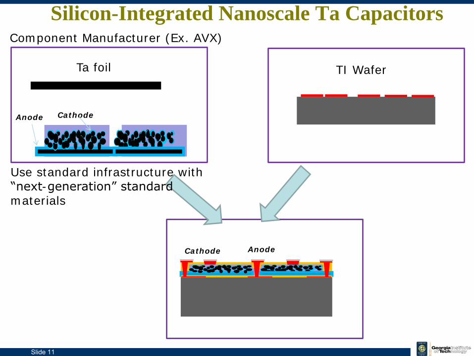
Ta foil
Silicon-Integrated Nanoscale Ta Capacitors
AnodeCathode
Anode Cathode
Component Manufacturer (Ex. AVX)
TI Wafer
Use standard infrastructure with “next-generation” standard materials

Slide 12
Parameters Si deep trench Discrete MLCC
Foil Capacitors
Component thickness (µm) ~ 200-300 200 75
Capacitance (µF/mm2) 1-2 2-3 2-3
Frequency (MHz) - 150 1 - 150
Leakage current (µA/µF) 0.1 0.01 0.01
Competitiveness of GT capacitors

Slide 13
Capacitor Reliability
65°C/95%RH for 1000 hours
• Capacitance response to frequency similar before and after exposure to elevated temperatures and moisture
• Improved ESR after testing• Parylene sufficient hermetic seal that removes need for casing
80 kA-8V200 nm Parylene
1.19 µF/mm2
at 1 MHz
1.09 µF/mm2
at 1 MHz
1.15 µF/mm2
at 1 MHz1.34 µF/mm2
at 1 MHz
65°C/95%RH for 500 hours
Slide 14
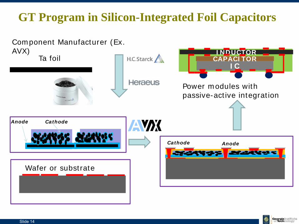
GT Program in Silicon-Integrated Foil Capacitors
Ta foil
Anode Cathode
AnodeCathode
Component Manufacturer (Ex. AVX)
Wafer or substrate
ICCAPACITOR INDUCTOR
Power modules with passive-active integration

Slide 15
Why high-voltage and high-temp capacitors:
High-power inverter and battery chargers:
• DC link capacitors;(suppress noise from pulsed
inverter current and stray DC
bus inductance)
Key challenges:• Higher voltage (200-900 V)• High-temperature stability (115-175) • Higher volumetric density for miniaturization
Wolfspeed

Slide 16
High-Temperature and High-Voltage Capacitors
AMS’ metallized polymer film capacitors
EPCOS: MLCCs with PLZT11 microfarad/cc; 350 V
700 V; 625 A current;68 mm x 34 mm x 30 mm
Safron’s olymer film capacitors
Electrolytic capsVishay
Operating voltage
Capacitance Case-size (in mm)
400 V 120mFDiameter: f25 mmLength: 30 mm
400 V 68mF Diameter: f20Length: 30 mm
400 V formed dielectric

Slide 17
Theoretical versus Achieved Volumetric Density for 450 V Applications
0.000
10.000
20.000
30.000
40.000
50.000
60.000
70.000
80.000
Polymer film Al Foil Cu with hybrid HV MLCC(CZT)
HV MLCC(PLZT)
Cap
acit
an
ce D
en
sit
y
(n
F/
mm
3o
r m
icro
farad
/cm
3)
PRC approach
Technology Gap(between current status and theoretically achievable)

Slide 18
Thin Planar HV and HT Capacitors
– Porous copper electrodes with hybrid dielectrics
– Layering with high thermal conductivity adhesives
– High thermal-stability adhesives– Vias and metallization– Solder termination with through-vias– 3D stacking for unlimited scaling up in
capacitance
8-9 microfarad/cm3
450 V85-115 C
40 microfarad/cm3
450 V>175 C
Porous copper Electrode
Conformal counter electrode
Slide 19
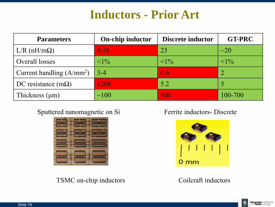
Parameters On-chip inductor Discrete inductor GT-PRC
L/R (nH/mΩ) 0.18 23 ~20Overall losses <1% <1% <1%Current handling (A/mm2) 3-4 0.6 2DC resistance (mΩ) 1200 5.2 5Thickness (μm) ~100 900 100-700
Inductors - Prior Art
Sputtered nanomagnetic on Si Ferrite inductors- Discrete
Coilcraft inductorsTSMC on-chip inductors

Slide 20
Advanced Magnetic Substrates
Nitto Denko Corporation
Substrate
Polymer insulation Magnetic sheets
Copper winding
IC IC
v vv
Laminate substrate
Copper winding
Magnetic film
Magnetic film
20

Slide 21
Inductors IPDs with Nanomagnetic Films on 50 microns glass
Inductor: T=10um
Glass: T=100um
Oxide: T=0.1umNanomagnetic film: T=0.2um
3 layers at the bottom: 3 nanomagnetic films
& 3 Oxides
3 layers at the top: 3 nanomagnetic films
& 3 Oxides
1 layer at the center: 1 nanomagnetic film
: T=10 um
Potcor or racetrack inductors
Solenoid inductors
0
10
20
30
40
50
60
70
0 5 10 15 20 25 30 35
Ind
uctan
ce (nH
)
Magnetic inductors
~10X enhancement in inductance
0
100
200
300
400
500
600
700
800
900
1000
1.E+07 1.E+08 1.E+09
Perm
eabi
lity
Frequency (Hz)
Real
Imag
Frequency (MHz)
Slide 22
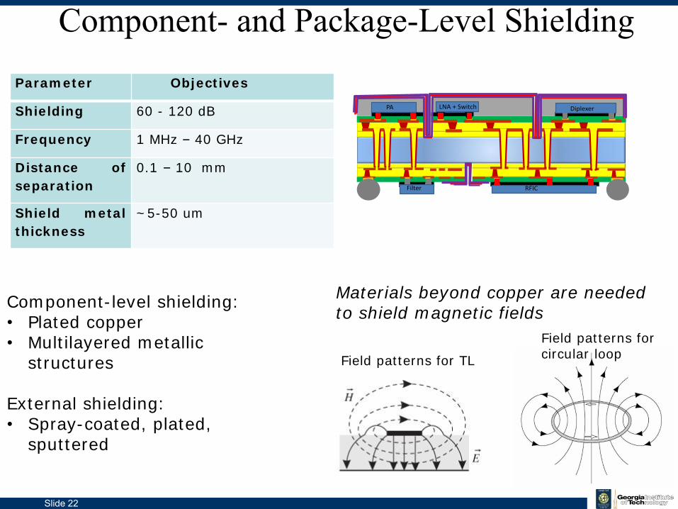
Parameter Objectives
Shielding 60 - 120 dB
Frequency 1 MHz – 40 GHz
Distance of
separation
0.1 – 10 mm
Shield metal
thickness
~5-50 um
Filter
DiplexerLNA + SwitchPA
RFIC
Component- and Package-Level Shielding
Field patterns for TL
Field patterns for circular loop
Materials beyond copper are needed to shield magnetic fields
Component-level shielding:• Plated copper• Multilayered metallic
structures
External shielding:• Spray-coated, plated,
sputtered

Slide 23
Unique Approach
Multilayered shields
Multiple reflections inside the shield
– More effective shielding lower shield thickness
– Effective at lower frequencies when absorption is not effective
Package-Level Shielding Beyond Copper and Mu metal
Shielding effectiveness1. Absorption loss (A)2. Reflection loss (R)
Incomingwave
Weak secondary wave
High impedance
Low impedance
• Magnetic films and magnetic absorption materials
EM
I Shie
ldin
g
Thickness

Slide 24
1 2 3 4 5 6 7 8-70
-60
-50
-40
-30
-20
Isol
atio
n (d
B)
Separation Distance (mm)
1 2 3 4 5 6 7 8-80
-70
-60
-50
-40
Isol
atio
n (d
B)
Separation Distance (mm)
NiFe+Ti
Cu(7)NiFe(3)Cu(3)NiFe(7)Ti
NiFe Cu No shield
NiFe+Ti
Cu(7)NiFe(3) Cu(3)NiFe(7)Ti
NiFeCu
No shield
Better EMI isolation Over Cu with Cu-Magnetic structures
(a)
(b)
(a)
(b)
Slide 25
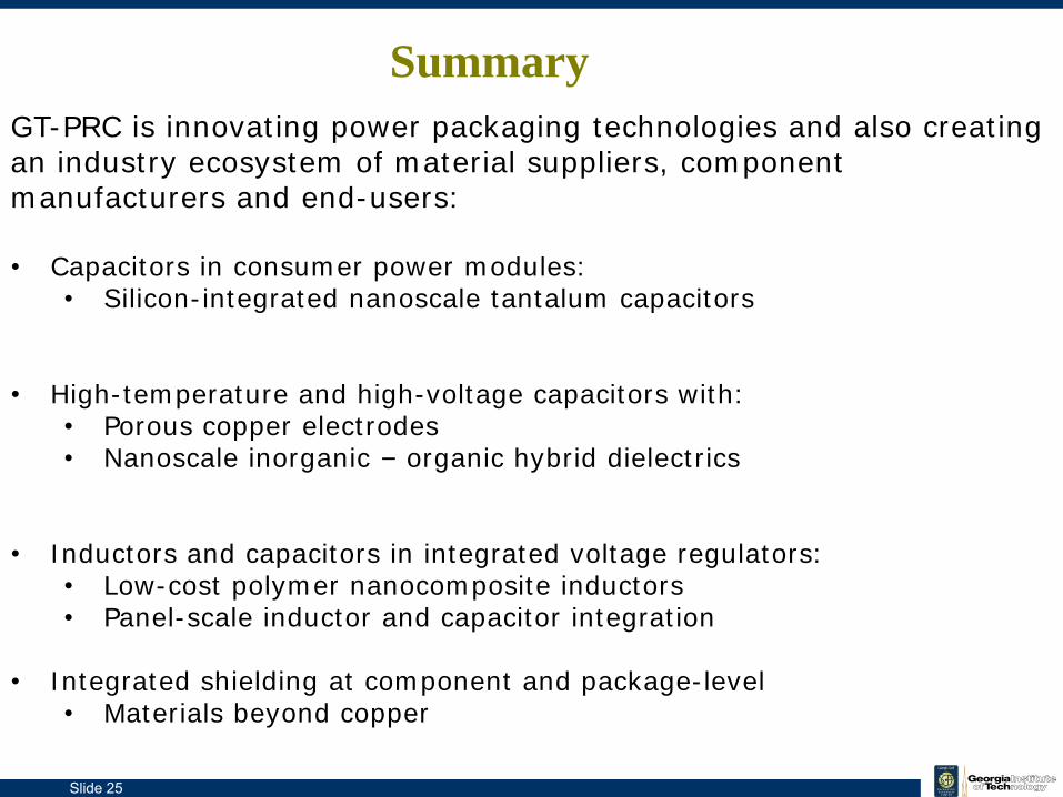
Summary
GT-PRC is innovating power packaging technologies and also creating an industry ecosystem of material suppliers, component manufacturers and end-users:
• Capacitors in consumer power modules:• Silicon-integrated nanoscale tantalum capacitors
• High-temperature and high-voltage capacitors with:• Porous copper electrodes• Nanoscale inorganic – organic hybrid dielectrics
• Inductors and capacitors in integrated voltage regulators:• Low-cost polymer nanocomposite inductors• Panel-scale inductor and capacitor integration
• Integrated shielding at component and package-level• Materials beyond copper