power electronicsee.cet.ac.in/downloads/notes/pe/pe2-firingcct.pdf · in a resistance firing...
TRANSCRIPT

Power Electronics
TRIGGERING CIRCUITS
DEPT. OF ELECTRICAL ENGINEERING, COLLEGE OF ENGINEERING TRIVANDRUM 1
2018 Dr. Francis M. Fernandez

Gate Characteristics
DEPT. OF ELECTRICAL ENGINEERING, COLLEGE OF ENGINEERING TRIVANDRUM 2
OA and OB represent the spread of characteristics for the thyristor of same rating
Vg
Ig
Vgmax
Vgmin
Igmin IgmaxO
B
A
E
S1
S2

R - Triggering Circuit
DEPT. OF ELECTRICAL ENGINEERING, COLLEGE OF ENGINEERING TRIVANDRUM 3
1
maxR
VI m
g max
1
g
m
I
VR
R1 is the gate current limiting resistance
R2 is used to vary the gate current and hence firing angle
max
1max
gm
g
VV
RVR
R limits the voltage at Gate terminal
Diode D prevents build-up of negative voltage at Gate terminal
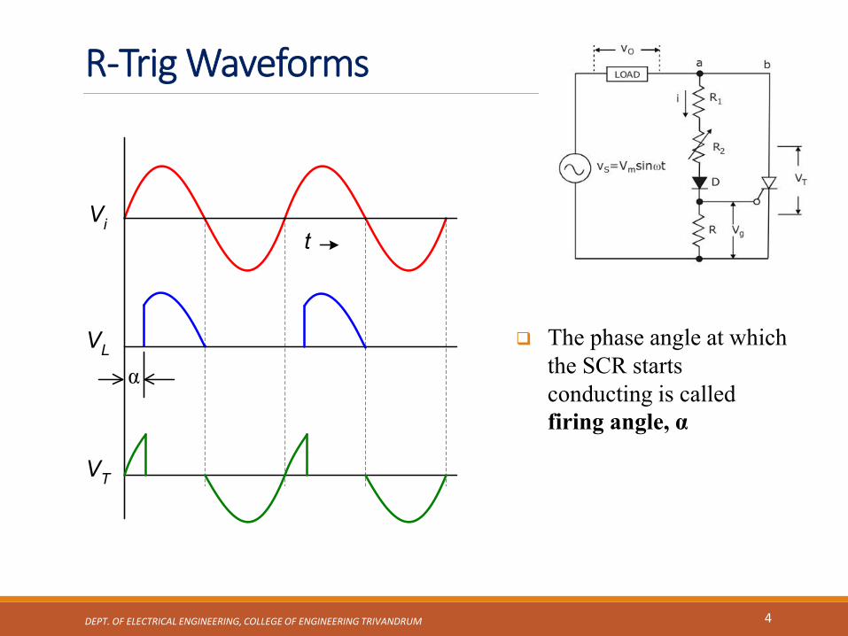
R-Trig Waveforms
DEPT. OF ELECTRICAL ENGINEERING, COLLEGE OF ENGINEERING TRIVANDRUM 4
Vi
VL
VT
t
α
The phase angle at which the SCR starts conducting is called firing angle, α
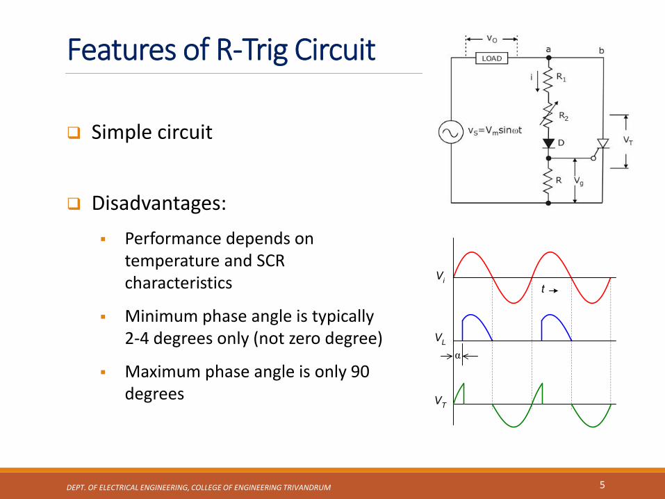
Features of R-Trig Circuit
DEPT. OF ELECTRICAL ENGINEERING, COLLEGE OF ENGINEERING TRIVANDRUM 5
Vi
VL
VT
t
α
Simple circuit
Disadvantages:
Performance depends on temperature and SCR characteristics
Minimum phase angle is typically 2-4 degrees only (not zero degree)
Maximum phase angle is only 90 degrees

Problem
Design an R-triggering circuit for a half wave controlled rectifier circuit for 24 V ac supply. The SCR to be used has the following data.
Igmin = 0.1 mA, Igmax = 12 mA, Vgmin = 0.6V, Vgmax = 1.5 V
6DEPT. OF ELECTRICAL ENGINEERING, COLLEGE OF ENGINEERING TRIVANDRUM
�� = 24 2 1 3max
24 22.8 3.3
12 10m
g
VR k k
I
� ≤�������
�� − �����=1.5 × 3.3 × 10�
24 2 − 1.5= 145.8 � ≃ 120 �
�����
�� − �����=
�
�� + ��
�� =�� − ����� �
�����− �� =
24 2 − 0.6 × 120
0.6− 3.3 × 10� = 3.37 ��
For finding R2
Select 4.7 k Potentiometer for R2(Drop across diode D is neglected)
Solution:

Problem
DEPT. OF ELECTRICAL ENGINEERING, COLLEGE OF ENGINEERING TRIVANDRUM 7
In a resistance firing circuit for SCR, the following parameters are applicable
Igt(min) = 0.5 mA,
V gt(min) = 0.7V,
Supply voltage = 48 V, 50Hz
Resistance in gate current path = 70 kΩ.
a) Find the firing angle for the abovecondition
b) What is the resistance for which firing angle is 90 degrees

Solution
DEPT. OF ELECTRICAL ENGINEERING, COLLEGE OF ENGINEERING TRIVANDRUM 8
V3.36
7.06.01070105.0 33
21
gDgt VVRRIe
1
sin
36.3 2 48sin
36.3sin 0.535
2 48
sin 32.3
t me V t
t
t
t t
Firing angle = 32.3 degrees
a)

Solution
DEPT. OF ELECTRICAL ENGINEERING, COLLEGE OF ENGINEERING TRIVANDRUM 9
kΩ133105.0
6.66
105.06.66
7.06.0105.0482
3
3
3
21
R
R
R
VVRRIe gDgt
b)

RC Triggering Circuit
DEPT. OF ELECTRICAL ENGINEERING, COLLEGE OF ENGINEERING TRIVANDRUM 10
Capacitor charges during the negative half cycle through D2
When SCR is turned on, capacitor C is suddenly discharged through D2
D1 protects the SCR during negative half cycle
2
3.1 TRC
1min mins g g Dv R I V V
To ensure minimum gate current
1min
min
s g D
g
v V VR
I
Advantage over R-triggering Circuit:
Controls upto 180 degrees

RC Trig Waveforms
DEPT. OF ELECTRICAL ENGINEERING, COLLEGE OF ENGINEERING TRIVANDRUM 11
2
3.1 TRC
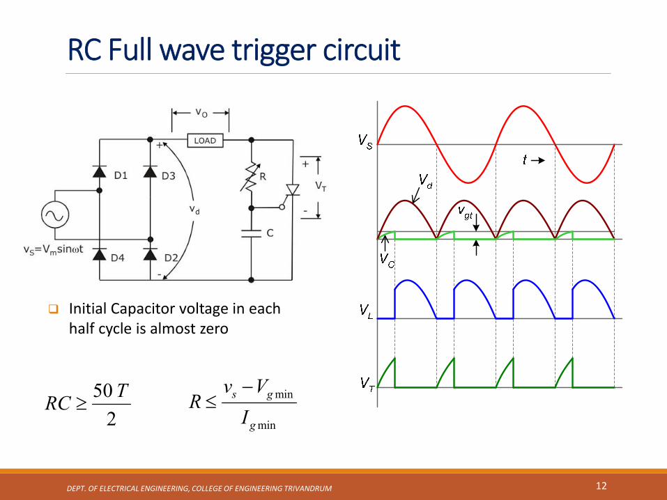
RC Full wave trigger circuit
DEPT. OF ELECTRICAL ENGINEERING, COLLEGE OF ENGINEERING TRIVANDRUM 12
2
50 TRC
Initial Capacitor voltage in each half cycle is almost zero
min
min
s g
g
v VR
I

Unijunction Transistor (UJT)
DEPT. OF ELECTRICAL ENGINEERING, COLLEGE OF ENGINEERING TRIVANDRUM 13
Has a lightly doped n-type silicon layer to which a heavily doped p-type emitter is embedded
The inter-base resistance is in the range of 5 – 10 kΩ
This device cannot ‘amplify’
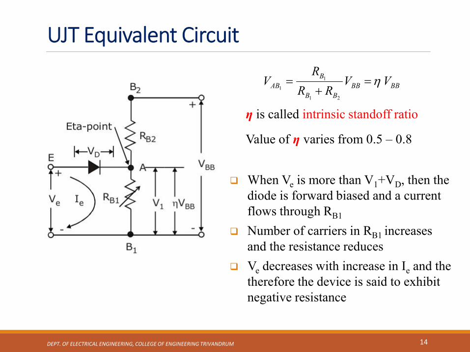
UJT Equivalent Circuit
DEPT. OF ELECTRICAL ENGINEERING, COLLEGE OF ENGINEERING TRIVANDRUM 14
BBBB
BB
B
AB VVRR
RV
21
1
1
η is called intrinsic standoff ratio
Value of η varies from 0.5 – 0.8
When Ve is more than V1+VD, then the diode is forward biased and a current flows through RB1
Number of carriers in RB1 increases and the resistance reduces
Ve decreases with increase in Ie and the therefore the device is said to exhibit negative resistance

UJT Characteristics
DEPT. OF ELECTRICAL ENGINEERING, COLLEGE OF ENGINEERING TRIVANDRUM 15
At peak point, Ve = V1+VD,
At Valley point, RB1 is minimum
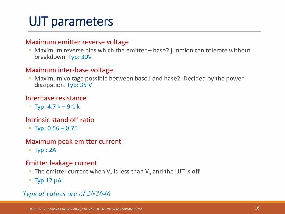
UJT parameters
DEPT. OF ELECTRICAL ENGINEERING, COLLEGE OF ENGINEERING TRIVANDRUM 16
Maximum emitter reverse voltage◦ Maximum reverse bias which the emitter – base2 junction can tolerate without
breakdown. Typ: 30V
Maximum inter-base voltage◦ Maximum voltage possible between base1 and base2. Decided by the power
dissipation. Typ: 35 V
Interbase resistance◦ Typ: 4.7 k – 9.1 k
Intrinsic stand off ratio ◦ Typ: 0.56 – 0.75
Maximum peak emitter current◦ Typ : 2A
Emitter leakage current◦ The emitter current when Ve is less than Vp and the UJT is off.
◦ Typ 12 μA
Typical values are of 2N2646
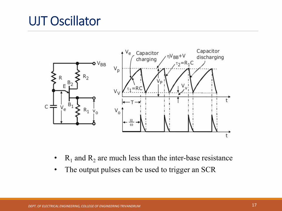
UJT Oscillator
DEPT. OF ELECTRICAL ENGINEERING, COLLEGE OF ENGINEERING TRIVANDRUM 17
• R1 and R2 are much less than the inter-base resistance
• The output pulses can be used to trigger an SCR

Design
DEPT. OF ELECTRICAL ENGINEERING, COLLEGE OF ENGINEERING TRIVANDRUM 18
RC
t
BBC eVV 1
Time required for C to charge from Vv to Vp is obtained as follows
RC
t
BBvDBBp eVVVVV 1
Assuming D vV V
RC
t
e1
1
1ln
1RC
fT
Tt ,case For this
R1 is selected based on voltage level required to trigger the SCR
R2 is selected using the empirical formula:
BBVR
4
2
10
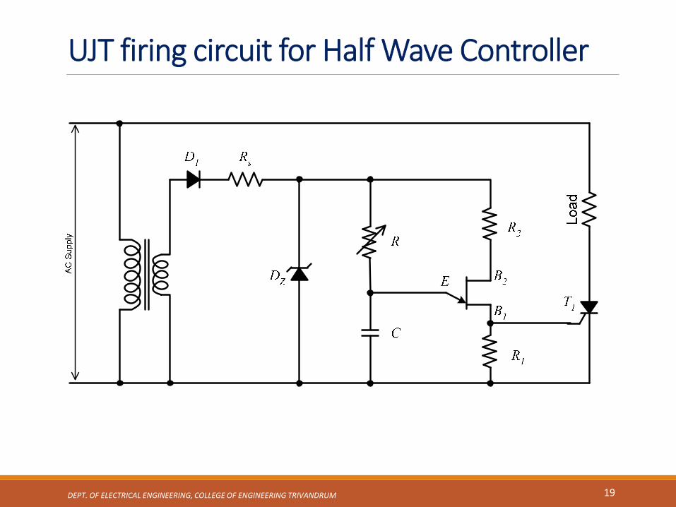
UJT firing circuit for Half Wave Controller
DEPT. OF ELECTRICAL ENGINEERING, COLLEGE OF ENGINEERING TRIVANDRUM 19
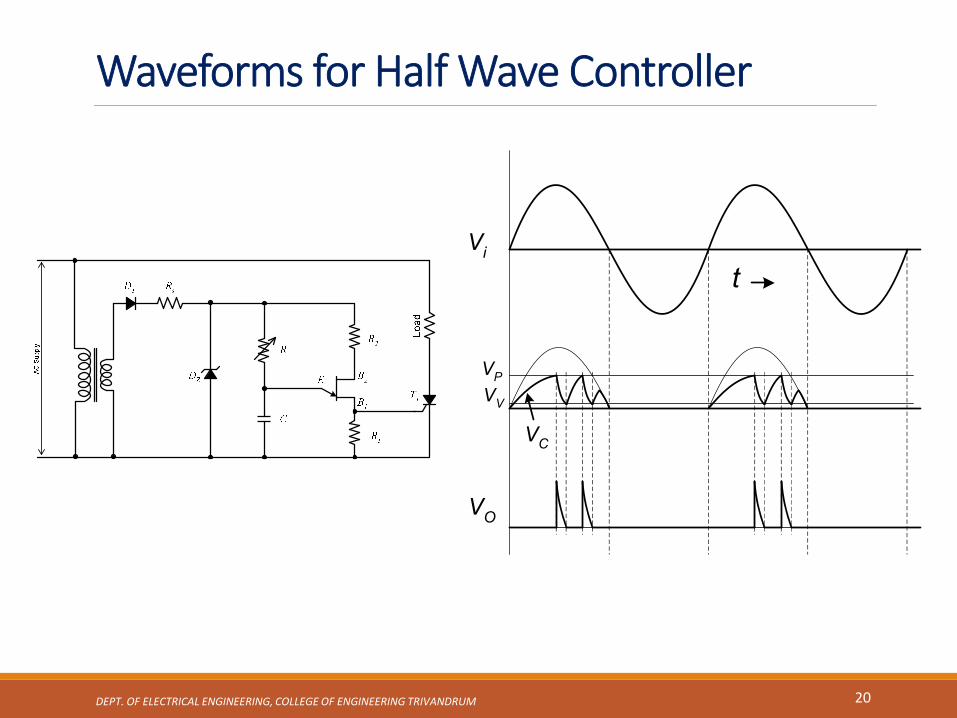
Waveforms for Half Wave Controller
DEPT. OF ELECTRICAL ENGINEERING, COLLEGE OF ENGINEERING TRIVANDRUM 20
Vi
VP
VO
t
VC
VV
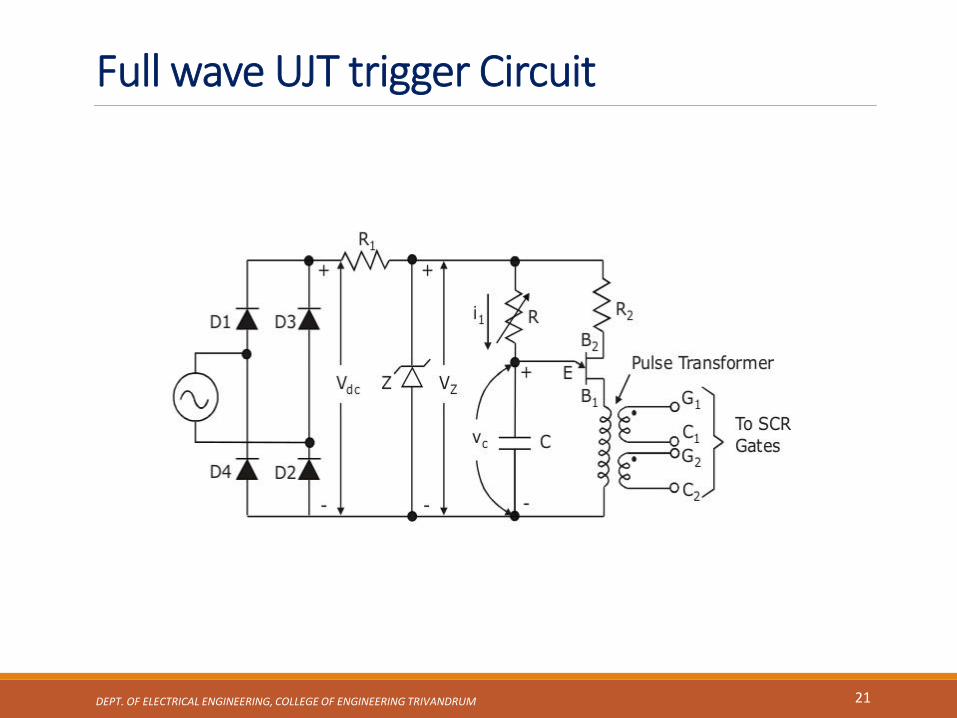
Full wave UJT trigger Circuit
DEPT. OF ELECTRICAL ENGINEERING, COLLEGE OF ENGINEERING TRIVANDRUM 21
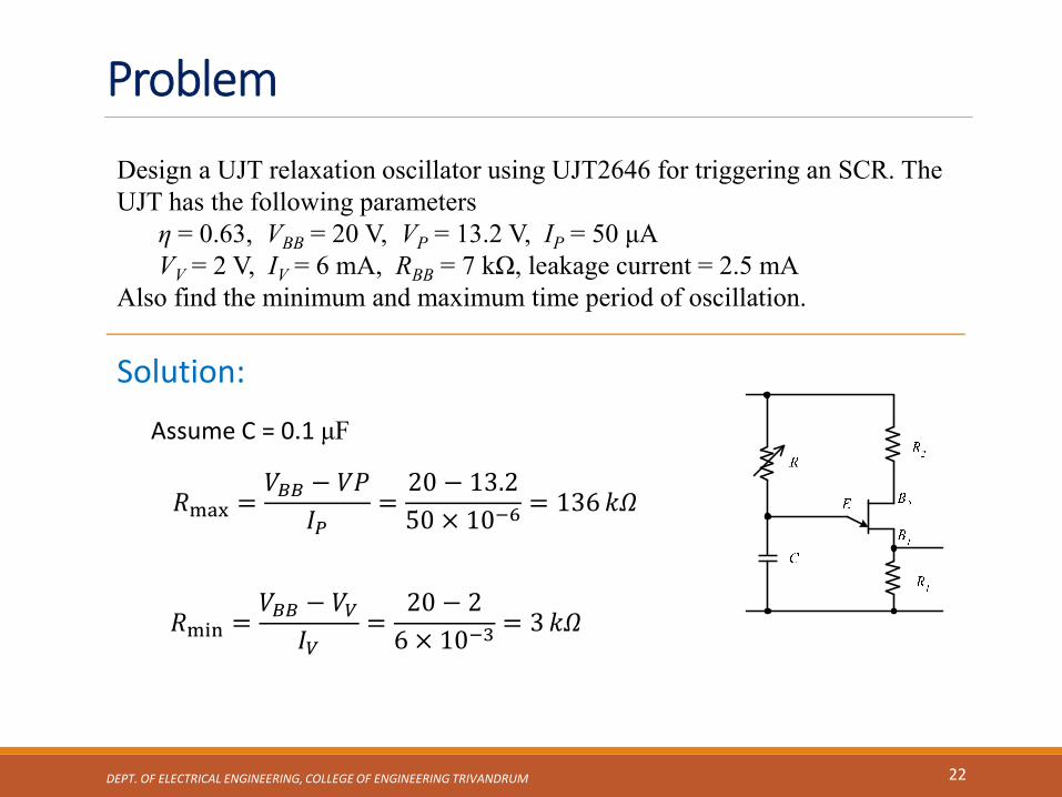
Problem
DEPT. OF ELECTRICAL ENGINEERING, COLLEGE OF ENGINEERING TRIVANDRUM 22
Design a UJT relaxation oscillator using UJT2646 for triggering an SCR. The UJT has the following parameters
η = 0.63, VBB = 20 V, VP = 13.2 V, IP = 50 μAVV = 2 V, IV = 6 mA, RBB = 7 kΩ, leakage current = 2.5 mA
Also find the minimum and maximum time period of oscillation.
Solution:
Assume C = 0.1 μF
���� =��� − ��
��=20 − 13.2
50 × 10��= 136 ��
���� =��� − ��
��=
20 − 2
6 × 10��= 3 ��

DEPT. OF ELECTRICAL ENGINEERING, COLLEGE OF ENGINEERING TRIVANDRUM 23
Approximate value of �2 =10�
� ���=
10�
0.63 × 20= 794 Ω
�� =�����
������� �������=
0.7
2.5 × 10��= 280 Ω
���� = ��ln1
1 − �= 136 × 10� × 0.1 × 10�� × ln
1
1 − 0.63= 13.5 ��
���� = 3 × 10� × 0.1 × 10�� × ln1
1 − 0.63= 0.3 ��

Commutation Commutation us the process by which a thyristor is turned off or
current diverted to another path.
There are two types of commutation Natural Commutation
Forced Commutation
24DEPT. OF ELECTRICAL ENGINEERING, COLLEGE OF ENGINEERING TRIVANDRUM
• In natural commutation, the reversing nature of alternating voltages turn off the thyristor
• Suitable for AC circuits only
• Current passes through a zero in every half cycle
• No external circuit is required for natural commutation
• In DC circuits, external circuits are necessary for turn off of thyristors
• Turn off with external circuits is called forced commutation

Pulse Transformer
DEPT. OF ELECTRICAL ENGINEERING, COLLEGE OF ENGINEERING TRIVANDRUM 25
Used to trigger SCR, TRIAC etc
Provides Electrical isolation between power circuit and control circuit

Optical Isolation
DEPT. OF ELECTRICAL ENGINEERING, COLLEGE OF ENGINEERING TRIVANDRUM 26
Used to trigger SCR, TRIAC etc
Provides Electrical isolation between power circuit and control circuit