power control intelligent motion ... - power systems design · pdf fileseptember 2006 power...
TRANSCRIPT

S e p t e m b e r 2 0 0 6
P o w e r f o r A u t o m o t i v ea n d H y b r i d E l e c t r i c V e h i c l e A p p l i c a t i o n s
P o w e r f o r A u t o m o t i v ea n d H y b r i d E l e c t r i c V e h i c l e A p p l i c a t i o n s
MarketwatchMarketwatchAutomotive ElectronicsAutomotive Electronics
ISSN: 1613-6365
Power Control Intelligent Motion

3www.powersystemsdesign.com
ViewpointDriving Solutions from Engineering ............................................................................................................................................................... 2
Industry NewsON Semiconductor Names Bob Mahoney Executive Vice President of Global Sales and Marketing ........................................................... 4
Collaboration for 45nm low-power process technology ................................................................................................................................ 4
China EMS Providers Expand...................................................................................................................................................................... 4
Intersil Promotes Roberto Magnifico to Vice President of European Sales ................................................................................................... 6
Infotainment Set to Boom in China ................................................................................................................................................................ 6
Philips Semiconductors to become NXP....................................................................................................................................................... 6
Power Events ............................................................................................................................................................................................... 6
New Dual Synchronous Step-Down DC/DC Converter Delivers 300mA/Ch from a 3mm x 2mm DFN ......................................................... 8
Practical Efficiency in Lighting Made Possible by Power Electronics, By Kevin Parmenter, Fairchild Semiconductor ................................. 10
MarketwatchFragmentation Increases in WW Power Management Market, By Marijana Vukicevic, iSuppli Corporation ................................................ 12
Cover StoryPower for Automotive and Hybrid Electric Vehicle Applications, By Peter Sontheimer, Tyco Electronics and Arno Mathoy,
Brusa Elektronik AG .................................................................................................................................................................................. 14
Focus on Automotive Electronics
Automotive / Power MOSFETsDesign for Operation in the Automotive Electrical Environment, By Mitchell Lee, Hua (Walker) Bai & Jeff Witt, Linear Technology .............. 24
Automotive / Thermal ControlTaking the Heat out of Automotive, By Nico Bruijnis, The Bergquist Company ........................................................................................... 29
Automotive / Power ManagementThe Lowest Quiescent Current Wins!, By Michele Sclocchi and Frederik Dostal, National Semiconductor ................................................. 32
Automotive / Power Semiconductor DesignEssential Design Criteria for Variable Automotive Power Semiconductors, By Bob Christie, Allegro Microsystems ................................... 35
Automotive / LCDsThe Needs and Benefits of Automatic Brightness Control Today’s Growing World of LCD Displays, By Roger Holliday, Microsemi ......... 39
Automotive / SensorsPre-empting Problems in the Automotive Environment, By John Constantopoulos, Texas Instruments ...................................................... 42
New Products ..........................................................................................................................................................................................45
CONTENTS
Power Systems Design Europe Steering Committee Members
Member
Eric Carroll
Arnold Alderman
Heinz R edi
Claus Petersen
Paul Greenland
Dr. Reinhold Bayerer
Kevin Parmeter
Dr. Leo Lorenz
Davin Lee
Eric Lidow
Representing
ABB Switzerland
Anagenesis
CT-Concept Technology
Danfoss
Enpirion
eupec
Fairchild Semiconductor
Infineon Technologies
Intersil
International Rectifier
Member
David Bell
Hans D. Huber
Ralf J. Muenster
Michele Scolcchi
Kirk Schwiebert
Christophe Basso
Balu Balakrishnan
Uwe Mengelkamp
Peter Sontheimer
Representing
Linear Technology
LEM
Micrel
National Semiconductor
Ohmite
On Semiconductor
Power Integrations
Texas Instruments
Tyco Electronics
Content.p65 2006-9-18, 10:322-3

VIEWPOINT VIEWPOINT
3www.powersystemsdesign.comPower Systems Design Europe September 20062
Well, here we go into the much publicizedAutomotive theme. I say much publicized,not so much from an editor’s perspective, butthat of an industry watcher. It looks, on thesurface, especially to a marketeer to be amuch lusted after segment realizing hugevolumes at good AUP. But is it all it seems?
There are characteristics found in automo-tive not typical of the general semiconductormarket. According to Databeans, the consis-tent demand for automotive electronics isgrowing faster than the vehicle market itself,as regulations tighten in emission standardsand safety requirements, and as consumersinvest in the DVD players and audio productsmade specifically for automotive applications.Sounds like a dream come true...
Legislated regulations and consumerdemands continue to drive this marketupward. High growth application areas forautomotive semiconductors include safety(airbags, cruise control, collision-avoidance,anti-lock brakes) and ‘cockpit electronics’(entertainment, telematics, instrumentation,phones). All of these applications have aneed for the parts in our power industry, sowhat could be the real advantages andperhaps drawbacks? As always inengineering, things are not quite so simpleand clear cut...Find out in this issue.
We look at the products on offer. Productswhich are innovative and highly specialized tothe automotive specification from a wide varietyof suppliers, but what I want to try to do is notjust present an array of silicon alternatives butto show real-world problems and solutions. Thismagazine is made for the design engineer and Iwant the content to be of use as well as ofinterest. We all have our ‘challenges’ toovercome on a daily basis and I would hopethat this magazine can be a forum for engineers.To present their own experiences and to sharewith colleagues in the industry.
After the much looked forward to holidayseason in July-August, the kids go back toschool and we are, as usual, plungedstraight into the rigours of work.
It occurred to me that when I thought aboutautomotive, I just thought about a specialclass of products optimized for reliability undertough conditions but as I edited our richselection of contributed articles and newsstories I learned there was far more to it thanthis simple theme. This is where the expertsconnected with our magazine show their greatvalue and insights for our collective benefit.
I would just like to take this opportunity toextend a warm welcome to two such expertsjoining our magazine.
Marijana Vukicevic, senior analyst,power management for iSuppli corporation.She will be contributing the Marketwatchsection of the magazine starting in this issueand Michele Sclocchi, principal applicationengineer, power management for Nationalsemiconductor Europe is the newest memberof our valuable steering committee.
In my recent visits to power semiconductorsuppliers, I am almost immediately impressedhow well aligned they are becoming with theproblems faced in engineering... real problems.This has not always been the case. The daysof the simple ‘silicon vendor’ are over, hope-fully forever and the new breed of ‘solutionprovider’ will ultimately win through.
But back to me. Luckily, my publisherhandles all the complicated stuff like circula-tion profiles (who needs to get it) and Adrevenues (who pays for it) and I just get thegood materials using our industry experts(steering committee plus authors) and todeliver this material for our mutual benefit.
Sounds like a dream job. It is. And with thedynamic and exciting nature of the powerindustry especially, it is definitely at one ofthe cutting edges of engineering and keepsus all on high alert. Long may it continue.
Cliff KeysEditor-in-Chief, [email protected]

Power Systems Design Europe September 20064
INDUSTRY NEWS
IBM, Chartered SemiconductorManufacturing, Infineon Technologies andSamsung Electronics Co., Ltd. todayannounced first silicon-functional circuits andthe availability of design kits based on theircollaboration for 45nm low-power processtechnology. The early characterization of keydesign elements in silicon, coupled with theavailability of early design kits, providedesigners with a significant head start inmoving to the latest process from theindustry-leading CMOS technology researchand development alliance. The early designkits are developed through a collaborativeeffort by all four companies and are immedi-ately available for select customers.
The first working circuits in 45nm
technology, targeted at next-generationcommunication systems, were proven insilicon using the process technology jointlydeveloped by the alliance partners and wereproduced at the IBM 300-millimeter (mm)fabrication line in East Fishkill, NY, where thejoint development team is based. Among thesuccessfully verified blocks are standardlibrary cells and I/O elements provided byInfineon, as well as embedded memorydeveloped by the alliance. Infineon hasincluded special circuitry on the first 300mmwafers to debug the complex process and togain experience in product architectureinteractions.
The development of the design kitsincorporates design expertise from all four
ON Semiconductor Names Bob Mahoney Executive VicePresident of Global Sales and Marketing
ON Semiconductor Names Bob MahoneyExecutive Vice President of Global Salesand Marketing
ON Semiconductor, a leading industrysupplier of power solutions, has named BobMahoney Executive Vice President of GlobalSales and Marketing. Mr. Mahoney takes onhis new responsibilities after successfullydirecting the company’s Sales for theAmericas as Vice President. During his tenurewith ON Semiconductor, Mr. Mahoney hasbeen instrumental to the company’s growthof market share and bottom line profitability.Since joining the company in 2003, he hasheld executive responsibilities throughoutthe sales organization—including VicePresident of Global Distribution and theElectronic Manufacturing Services Industry(EMSI), and Vice President of North AmericaSales, Computing Segment Sales and SalesOperations.
“To accelerate the growth of ONSemiconductor’s power solutions portfolio,the company was internally realigned at thebeginning of the third quarter into four market-based divisions—namely the Digital andConsumer Products Group, the ComputingProducts Group, the Automotive and PowerRegulation Products Group and the StandardComponents Group,” said Mr. Mahoney.“My first order of business is to better align
ON Semiconductor’s worldwide sales andmarketing efforts to meet the engineeringneeds and manufacturing challenges of ourexisting and future customers in these focusapplication areas.”
Mr. Mahoney brings more than 20 yearsof semiconductor industry experience insales and sales management to his new roleas Executive Vice President of Global Salesand Marketing for ON Semiconductor. Justprior to joining the company, he was VicePresident of World Wide Sales for XicorSemiconductor. Previously, at Altera, he wasVice President of Strategic Accounts. Duringhis career, he has also held sales manage-ment roles at Analog Devices and NationalSemiconductor.
Mr. Mahoney holds both a BA and aMasters degree in Business Administrationfrom LaSalle University. He replaces BillBradford—who left ON Semiconductor toaccept a position with FreescaleSemiconductor.
http://www.onsemi.com
companies in order to facilitate the earliertransition to the new process by chipcustomer designers, as well as continue todrive single-design, multi-fab manufacturingcapability for maximum design leverage andto bring about ultimate consumer benefit.The 45nm low-power process is expectedto be installed and fully qualified atChartered, IBM and Samsung 300mm fabsby the end of 2007.
Collaboration for 45nm low-power process technology
Electronics buyers who are involved inoutsourcing decisions can expect electronicsmanufacturing services (EMS) providers inChina to diversify their manufacturingcapabilities in China and expand into lessdeveloped areas to take advantage of lowerlabor rates.
Some EMS companies in China arefocusing more attention on automotive andmedical electronics. For instance, SurfaceMount Technology, a Hong Kong-basedEMS provider, has established factories in
China EMS Providers Expand
www.pcb007.com/china.aspx
Changchun City in Kilin Province and Tianjinto add capacity for automotive electronicsproducts. China First Automotive WorksGroup, China’s largest automaker, is a majorcustomer of Surface Mount Technology.
The automotive electronics market in Chinais expected to grow from about $4 billion in2004 to more than $7 billion in 2010, saysresearcher iSuppli.
Some companies are migrating to low costareas. EMS providers have been located inthe Pearl River Delta, Yangtze River Delta
and Bohai Gulf. Now some EMS providersare starting to expand into the northeast andmid-western areas of China.
The migration is occurring because of labourand power shortages in the Yangtze andPearl River delta areas. However, as EMScompanies migrate, there are challengesincluding complicated logistics managementbecause of fewer transport links.
www.infineon.com
www.ibm.com
www.charteredsemi.com
www.samgsungsemi.com

Power Systems Design Europe September 20066
INDUSTRY NEWS
Intersil Promotes Roberto Magnifico to Vice President ofEuropean Sales
Intersil announces the promotion ofRoberto Magnifico to the position of VicePresident of Sales, Europe, located atIntersil’s sales office in Lausanne,Switzerland.
Magnifico joined Intersil in 1997 as amarketing manager and progressed to salesdirector for Europe in 2002. As Sales Directorhe helped drive sales growth and improveIntersil’s overall brand in the region. As VicePresident, Mr. Magnifico will play a vitalleadership role in Intersil’s efforts to re-enterthe automotive market and further penetrate
key OEM electronics customers throughoutEurope.
“I expect that Roberto’s continuedleadership in the region will allow Intersil toexpand its presence in Europe, go afterstrategic growth markets and engage withnew customers,” said Peter Oaklander,Intersil’s senior vice president of WorldwideSales. “Roberto’s strong sales background,as well as his long tenure with Intersil and inthe semiconductor industry, makes himideally suited for these expandedresponsibilities.”
Mr. Magnifico has been in the semicon-ductor industry since 1984. Prior toIntersil, Mr. Magnifico worked for PhillipsSemiconductor for nine years. He beganhis career in 1984 at STMicroelectronicsas a product engineer in the Power AudioAmplifier ICs product group. Mr. Magnificoholds a BSEE from L. Settembrini, MilanoTech Institute.
www.intersil.com
With a change of ownership from RoyalPhilips Electronics to a consortium of privateequity investment companies, PhilipsSemiconductors will simply become NXP.
NXP stands for the consumer’s “nextexperience,” according to CEO Frans vanHouten. NXP is also associated with PhilipsSemiconductors’ Nexperia platform whereaudio and video processing technologiesreside.
The NXP trademark will include a “Foundedby Philips” tagline as part of its branding.“We want to create the bridge between the‘next experience’ and our rich heritage,” saidvan Houten. “We have agreed as part of the
Philips Semiconductors to become NXPdisentanglementthat we can use thePhilips brand link toNXP.”
In an interview,van Houton laid outseveral newbusiness priorities.First, NXP isplanning a strategicinvestment incellular basebandtechnologies inorder to save whatappears to be alacklusterbasebandbusiness. Themove would also
help it gain substantial market share in themobile wireless sector.
NXP will also make a sizable investment indevelopment tools to increase productquality. “Quality, too often, has become anodd one out,” he said, suffering at theexpense of the company’s pursuit of "costand time-to-market.
“If you have to re-spin your SoC threetimes to get it right, you are not only deliver-ing a product to your customers nine monthslate, but you are also increasing the cost ofdevelopment,” he said.
Citing massive recalls of notebookcomputers with faulty batteries in recent
Infotainment Set to Boom in ChinaThe Chinese domestic market for
infotainment—vehicle entertainment andnavigation systems—will be worth at least$4 billion by 2013, according to research byanalysis firm Strategy Analytics.
The market opportunity will be dominatedfor some time by the vehicle OEM business,the firm reported today, and the domesticaftermarket will not become significant until2007 and onward.
Additionally, there are significant costreduction opportunities for any internationalinfotainment system vendor willing to investin China, Strategy Analytics said, andJapanese vendors like Clarion, Pioneer,Kenwood and Panasonic are leading thischarge.
“For international automotive infotainmentsystem suppliers, China offers opportuni-ties to reduce component and system
production costs, to increase access tointernational/Chinese vehicle OEM jointventures, and to respond to the growingdomestic Chinese OE market,” JoanneBlight, director of the Strategy Analyticsautomotive multimedia and communicationsservice, said in a statement.
www.strategyanalytics.net
www.nxp.com
weeks, van Houten noted, “We will neverwant to be the reason for recalled products.Quality is very important.”
Van Houten said NXP will “raise thedevelopment budget” for products, “seekingthe best tools.” He added, “We will notskimp on quality, and we will aim for zerodefect and first-time-right silicon.”
Power Events
� H2Expo, October 25-26, Hamburg,
www.h2expo.com
� ELECTRONICA 2006, Nov. 14 - 17, Munich,
www.electronica.de
� SPS/IPC/DRIVES 2006, Nov. 28 - 30,
Nuremberg, www.mesago.de/de/SPS/main.htm

Power Systems Design Europe September 20068
Linear Technology Corporation
announces the LTC3547, a dual
channel, high efficiency, 2.25
MHz, synchronous buck regulator that
delivers up to 300mA of continuous
output current per channel from a 3mm
x 2mm DFN package. Using a constant
frequency current mode architecture,
the LTC3547 operates from an input
voltage range of 2.5V to 5.5V, ideal for
single cell Li-Ion/Polymer, or multicell
alkaline/NiCad/NiMH applications. It
can generate output voltages as low as
0.6V, enabling it to power the latest
generation of low voltage DSPs and
Figure 1. Dual 300mA, 2.25MHz Synchronous Step-Down DC/DC Converter.
microcontrollers. Its 2.25MHz switch-
ing frequency enables the use of tiny,
low cost ceramic capacitors and
inductors less than 1mm in height,
providing a very compact solution
footprint for handheld applications.
The LTC3547 uses internal switches
with an RDS(ON) of only 0.75 Ohm (N-
Channel) and 0.80 Ohm (P-Channel) to
deliver efficiencies as high as 96%. It
also utilizes low dropout 100% duty
cycle operation to allow output volt-
ages up to VIN, further extending
battery run-time. The LTC3547 incor-
porates low ripple Burst Mode?
operation, offering only 40uA no load
quiescent current (both channels) with
only 20mVP-P of output ripple. Shut-
down current is less than 1uA, further
extending battery life. Each channel has
independent internal soft-start, en-
abling design flexibility. Other features
include short-circuit and over-tempera-
ture protection.
The LTC3547EDDB is available in an
8-lead 3mm x 2mm DFN package.
www.linear.com

Power Systems Design Europe September 200610
By Kevin Parmenter, FAE Director, Fairchild Semiconductor
I recently was asked by my son to
assist him with a project to reduce
the energy consumption of the
lighting in the parking and common
areas of his condominium complex
where he serves as the association
manager. As my son is a computer
science engineer he needed some
practical hardware assistance. Statis-
tics have shown according to the US
Department of Energy the average
home consumes 25% of its electrical
energy in the production of light. The
average school, store or commercial
building uses 60% of its electrical
consumption in lighting. This provides
an opportunity for improvement in
conversion efficiency for retrofitting with
newer more efficient technologies. As
my sons condo complex in Scottsdale,
Arizona the environment for temperature
testing is extreme and the lighting is
cycled daily on a photo switch with
plenty of sunshine to switch it. This
photo switch allows a reasonably
controlled environment to test the
electric bill difference with the exception
of the rising and setting times of the
sun changing from day to day over time.
For the past several decades lighting
options were limited there was
incandescent, mercury vapor, fluores-
cent or high pressure sodium the latter
having only magnetic ballasts
available. Electronics was unheard of in
these applications not all that long
ago. The growth of CFL lamps, elec-
tronic ballasts and UHB LED lighting
has seen rapid growth. In this particu-
lar condominium example the complex
is approximately 25 years old and no
electronics were present in anything
except the photo switch. The project
involved replacement of incandescent
lamps with Energy Star rated CFL
lamps and magnetic ballasts with
Energy Star electronic ballasts. Addi-
tionally we replaced the linear flores-
cent lamps with higher efficiency lamps
in existing fixtures. We made some
measurements of the current con-
sumption during these tests to check
the “before” and “after” to check the
difference in energy consumption. A
completely unscientific eyeball test was
performed to see what the difference in
lighting output was between the before
and after was also conducted.
So what were the results? The old
bulbs and ballasts were recycled so the
glass and metal were recovered and
reused – especially the copper is
important. The overall energy con-
sumption was predicted to be about
1/3 of what it was previously and
measured to approximate that figure
using simple DMM current
measurements. The light output
appeared to be equal to or better than
the previous lamps. The Installation
was simple because the original
fixtures were retained only the lamps
and ballasts were replaced (stated
differently the same sheet metal was
reused) Over the last three months of
reading the electric bill the consump-
tion has dropped by approximately two
thirds so the installation is generating
the same or greater light output on
approximately one third of the energy
as previously consumed.
In summary the cost effectiveness of
this retrofit considering the payback
period alone in power savings is highly
compelling. With the additional consid-
eration of less maintenance by not
having to replace incandescent lights
and the new linear florescent tubes are
“7 year lamps” it becomes very signifi-
cant indeed. What does this all mean?
With energy becoming more expensive
and less available all the time and with
green house gas emission being a
growing issue we all should be con-
cerned with conversion efficiency.
Considering humans are short circuit-
ing the normal sun - to producers and
consumer energy cycle in such a
manner that we appear to be causing
potentially irreversible damage to our
fragile planet we can make a difference
with power electronics.
This is exciting news for us in the
power electronics industry. Our tech-
nologies are no longer commodities
when we can make a difference such as
cutting lighting bills by two thirds and
increasing energy to light conversion
efficiency dramatically.
www.fairchildsemi.com

13www.powersystemsdesign.comPower Systems Design Europe September 200612
MARKET WATCH MARKET WATCH
By Marijana Vukicevic, iSuppli Corporation
Despite an abundance of suppli-
ers in the power management
semiconductor market, the
allure of these products is continuing
to attract new competitors to the
business, causing market share to
become more fragmented, according to
iSuppli Corp.
iSuppli tracks 248 significant semi-
conductor companies and of these, 109,
or 44 percent, are identified as suppliers
of power management devices. This is
despite the fact that power manage-
ment chips accounted for only $22
billion, or 9.3 percent, of global semi-
conductor consumption in 2005.
Such supply-heavy conditions might
be expected to trigger consolidation
among the market players, but in fact
the opposite is occurring, with the
number of significant competitors in
the power management space increas-
ing in 2005, according to iSuppli.
Power management semiconductors
present several attractions to potential
suppliers:
� Many power management semicon-
ductors are relatively easy to make,
and can be fabricated in fully depreci-
ated fabs that would otherwise be
under utilized.
� Manufacturers often want to
control power management functions
critical to the function of their own
proprietary chips.
� The wide variety of non-standard
applications means that a supplier can
succeed simply based on the special-
ized application expertise of a small
number of key employees.
� Many power chips, primarily custom
analog ICs, are among the most
profitable semiconductors made.
This has led to the fragmentation of
the supply base, a phenomenon that
should continue for some time, pre-
dicts iSuppli.
The top 20 suppliers are seeing their
share decline somewhat as new players
enter the market. The combined market
share declined to 74.9 percent in 2005,
down from 75.6 percent in 2004.
Looking at the top 20 players, North
American headquartered semiconduc-
tor suppliers continue to be aggressive
with respect to innovations in digi-
talized power, and have captured a
commanding lead in this area. These
suppliers have maintained a significant
lead in the power supply market, as
evidenced by the market success of
power supply focused companies such
as Texas Instruments, International
Rectifier, Fairchild, Microchip and
Linear Technology.
Texas Instruments and several
smaller North American headquartered
companies now are pushing forward a
new set of digital technologies that will
quickly and fundamentally alter the
competitiveness of many power supply
systems. This suggests that these
companies will maintain an advantage
in this area for some time to come,
unless major strides are made in
European and Japanese firms soon.
Looking at specific suppliers, number
two ranked Texas Instruments (of the
United States) distinguished itself by
posting the highest percentage in-
crease in power management semicon-
ductors in 2005 among the top 10
players, with a rise of 9 percent. The
company gained a half point of market
share during the year.
Texas Instruments has the greatest
momentum of the large power man-
agement suppliers, both from a
financial perspective and a technologi-
cal one. TI is regarded in the industry at
the moment as the company with the
best execution.
Mitsubishi Electric Corp. gained the
most market share of any power man-
agement company ranked by iSuppli in
2005, jumping from number 18 to
number 15 in the rankings and gaining
0.7 percentage point of market share.
Mitsubishi has made several innova-
tions in industrial and consumer
semiconductors, especially Insulated
Gate Bipolar Transistor (IGBTs), and
gained significantly in the market,
mostly at the expense of other Japa-
nese suppliers.
iSuppli anticipates that this momen-
tum will persist as Mitsubishi contin-
ues to introduce compelling new
packages and power chip technologies.
Marijana Vukicevic is the senior
analyst, power management for iSuppli
Corp. Contact her at
New players cause share to become more diverse
www.isuppli.com
E_MW.p65 2006-9-18, 10:0712-13

Power Systems Design Europe September 200614
COVER STORY
SoftSwing® inverters and customized powermodules for leaner and greener operation
Energy is getting more precious, yet we want to continuously be more mobile. A dilemma for the
automotive market.
By Peter Sontheimer, Tyco Electronics and Arno Mathoy, Brusa Elektronik AG
The human being is following
mega-trends in our world.
Boundless mobility as well as
the enjoyment of a clean and green
environment at home is an essential
desire in our daily life. The automotive
market reacts according to this
situation, well supported by both the
increasing fossil fuel cost and the
legislative environment, which de-
mands a decrease of CO2 emission
and fuel consumption. One possible
concept to answer such challenges is
the Hybrid Electric Vehicle HEV. The
Electronics industry is asked to react
and to come up quickly with suitable
solutions for today’s and tomorrow's
vehicle infrastructures. This article
analyzes a particular motor drive
inverter with a new topology, which
helps to reduce power losses as well
as EMI effects. It provides a deep
description of the core power element,
which shows a power module designed
for highest power density and
efficiency. The concept leads to better
silicon usage and to significant cost
reduction in the system.
Conceptual formulation
An inverter is under development for
the following applications:
� Automotive drives for hybrid and
fuel cell vehicles.� Hybrid bus traction or generator
inverter.� Drives for Streetcars, Trolleybuses,
Metros etc.� Turbine applications (Turbo-
generator, Compressor).� High speed machine tools.
In automotive applications, the focus
lies with the typical cyclic loadings
experienced whereas the machine tool
market requires in general longest
lifetimes in terms of operation
durability. As the inverter core electron-
ics are eventually required to be used in
mass volume vehicles, the focus is
maximum system cost reduction as
well as specific harsh mechanical
loading capability. The highest reliabil-
ity as well as power and current
densities must also be realized.
Among other components, a power
integrated module with lowest induc-
tances are under development in order
to achieve testable subsystem levels
which can entirely be qualified and can
be produced at constant quality levels,
reverting to most actual technologies
and fabrication processes.
SoftSwing® Inverter
The newly introduced inverter is based
on a resonant switching topology,
realizing the so called SoftSwing®
method. Besides a minimum of construc-
tion volume, the target for the inverter
design was to achieve extremely low
operation losses as well as a highly
improved EMI performance. In considering
these targets, a couple of design rules
regarding the power electronics were
considered in order to minimize the
system cost, arising while ramping up the
device in a mass production style manu-
facturing site. The system must have a
low internal complexity, consequent PCB
integration for passives, reduced overall
dimensions as well as weight regarding
its components, and must be realized
with an extremely low inductive design in
order to enable highest current handling
capability.The key was a high PWM-
frequency at low losses.
Functional principle and electri-
cal data
The inverter is operating at 150V..
450V level with maximum 600A
continuous current Irms
. The maximum
fundamental frequency supplied is
specified to 1700 Hz, whereas the
chosen PWM frequency runs with 24 kHz.

Power Systems Design Europe September 200616
COVER STORY
In general, the selected SoftSwing®
topology represents a full bridge power
circuit as shown in figure 1. By adding
a two phase transformer as well as
auxiliary capacitors in the circuit, a
resonant inverter topology can be
realized. The topology leads to signifi-
cant benefits within the system at
circuitry level, inverter level but also at
system level of the HEV:
Circuitry level� Prevents the IGBTs from absorb-
ing the reverse recovery charge when
the load current commutes from the
free wheeling diodes into the IGBT.� During turn off, the bridge capaci-
tors prevent the IGBTs from high
voltage as the tail current occurs.� Due to the absence of significant
switching losses, the IGBTs can be
utilized up to their rated DC-capability.� Ageing related to periodical
thermal expansion of the dye, caused
by adiabatic switching loss absorption
is completely avoided. SoftSwing® half
bridges have proven extremely rugged
and tolerant against overload.
Inverter level� Halves the required IGBT dye size
at 25kHz.� Allows the utilization of the body
drain diode in high voltage MOSFET
bridges.� Due to the absence of reverse
recovery spikes it generates extremely
low disturbance emissions. In
particular, DC-link filtering against
conducted emissions will be obsolete.
System level� SoftSwing®
enables a signifi-
cantly higher PWM-
frequency and thus
sinusoidal motor-
currents up to 2
kHz and even more.
This allows
innovative, high
power density
motor concepts.� High PWM-
frequency reduces
PWM related motor
losses and contrib-
utes to energy
savings.� Low du/dt
reduces dielectric
stress of the motor
insulation and
enhances thus
reliability during the
expected lifetime of
the vehicle.
Hardware de-
scription
Auxiliary
elements
The bridge point
formed by the two
main IGBTs is connected to an auxil-
iary circuit, consisting of small bridge
capacitors and an auxiliary half bridge
with small IGBTs and coupled induc-
tors on their drains.
Switching process and
characteristics
Figure 2 shows the switch-
ing behavior of the SoftSwing®
inverter. In case of active
switch-on, the external gate
stimulus turns on only the
auxiliary IGBTs which con-
ducts first (t0). Now, current
ramps up flowing into the
inductor. Due to the coupling,
the same current ramps up in
the other inductor through the
free wheeling diode of the
passive auxiliary switch.
Once the sum of these
auxiliary currents are equal to
the load current, the main free
wheeling diode is completely
prevented from any load
current and is about to set the bridge
point free (t1). Now the bridge capaci-
tors and the inductors form an LC-
oscillator and the bridge voltage starts
to swing around its neutral point, which
is in this case the virtual center tap of
the DC-link.
If the damping is sufficiently low, the
bridge voltage nearly reaches the other
rail potential where it is trapped by zero
current, zero voltage turn on of the
corresponding main IGBT (t2). From
this point, the auxiliary inductors give
off their stored energy as their currents
start to ramp down.
As the load current is continuously
flowing, the main IGBT current must
ramp in exchange of the disappearing
auxiliary current.
Once the load current is completely
commuted (t3), the inductors need to be
demagnetized, for which the auxiliary
IGBT has to be turned off (t4).
Figure 1. basic SoftSwing® topology.
Figure 2. switching process of the SoftSwing® inverter.
Figure 3. switching process of the main
and the pre-switch.

Power Systems Design Europe September 200618
COVER STORY
One solution to perform demagneti-
zation is formed by a well coupled
demagnetizing winding. Once the
auxiliary inductors are completely
demagnetized (t5) the half bridge is
ready for another active commutation.
Tradeoffs and limitations
The commuting time of course
affects the PWM. Generally the current-
depending turn on delay has to be
considered at the control part. In
addition, the demagnetizing time limits
the minimum turn on time to approxi-
mately 3% of the PWM cycle time.
Standard gate drivers cannot perform
well, in particular if they operate with a
fixed dead time. Any dead time will add
more turn on delay and is thus counter-
productive to SoftSwing®.
Power Module realization
In order to reach better performance
values and to achieve a defined and
electrically isolated thermal interface to
the inverter periphery a module technol-
ogy was selected. The power switches
define the core-element within the
application and significantly help to
increase current density within the
system as well as to decrease system
cost in mass production volumes.
The module is realized on a DBC
plate w/o a solid Cu-cooling plate. For
a better thermal interface to the cooling
medium AlN material was chosen. For
applications with lower power demand,
Al2O3 DBC can be equally selected,
although the chip can’t be used to its
full extent in this case. In the following
the AlN version is discussed. Figure 4
shows the electrical equivalent of the
power module.
600V module:
In order to achieve the required
performance levels, the module con-
tains for the main power bridge paral-
leled high speed IGBTs of the 2nd gen,
designed for fast switching
applications, with a given nominal
current of up to 50A each. The support-
ing transistors are single duos com-
posed of 3rd gen IGBTs and of high
efficiency fast recovery diodes.
1200V module:
The main power bridge contains
Tyco’s PhantomSpeed IGBTs, a
second generation transistor with
extremely high switching speed capa-
bility with a given nominal current of up
to 25A each, whereas the support
switches are composed of 3rd gen low
loss transistors. High efficiency Emcon
diodes complete the circuit.
Three such modules represent a
complete power kit of 40kW continuous
electrical power (VDC
= 75%VDCmax
, IAC
=
IACcont
, cosϕ = 0,9). The integrated
capacitors are SMD components,
specified for the required power and
voltage levels. An SMD thermistor is
integrated as well.
Following versions are completed:
Figure 4. electrical equivalent of the
SoftSwing® module.
Table 1. basic target characteristics of the selected power dice.
Power Systems Design Europe September 200620
COVER STORY
One important aspect regarding the
module development was to achieve
the lowest induction design. Figure 5
shows the selected pin arrangement
and outline of the module as well as
the power flow through the module.
Mechanical dimensions and
concept
SoftSwing® inverter
As of today the inverter is designed in
a solid Al-metal housing, whereas the
housing bottom is completed as a
water cooler. The outer dimensions are
unrivaled small for this power level:
� 88 x 240 x 360 mm, max. power 106
kW (VDC
= 75% VDCmax
, IAC
= IACmax
,
cosϕ = 0.9, 450V inverter).� 88 x 240 x 580 mm, max. power 212
kW (VDC
= 75% VDCmax
, IAC
= IACmax
,
cosϕ = 0.9, 900V inverter).
This leads to extreme performance
key figures of 11.1
kW/kg or 13,94 kW/
dm3 regarding the
450V inverter and of
14.1 kW/kg or 17,3
kW/dm3 regarding
the 900V inverter.
Figure 6 shows the
450V inverter,
comprising an
integrated terminal
box, which can
easily be adapted to
alternative
connectors.
Power Module
The power module circuit was
integrated in “flow 0” housing with a
DBC area of 39 x 28mm. The housing
itself relies on a 17mm mounting
height with integrated clip-in functions
as mechanical support to avoid
redundant mechanical stand-alone
parts on the heat sink. To avoid pin
stress caused by vibration, a defined
mechanical connection of PCB, power
module and heat sink is required. The
flow 0 housing concept ensures
robustness regarding vibration stress
and a stable thermal interfacing to the
heat sink [Mechanics and Electronics
as Instrument for Minimized Drive
Applications, Ralf Ehler, Michael Frisch,
PCIM Europe Conference 2004].
A flexible pin terminal structure
enables the realization of an application
optimized pin-out, by not exceeding
outer dimensions of 66mm x 32.5mm
x17mm, whereas PCB thicknesses of
1.0, 1.5 or 2.0mm respectively can be
chosen. Figure 7 shows the top view of
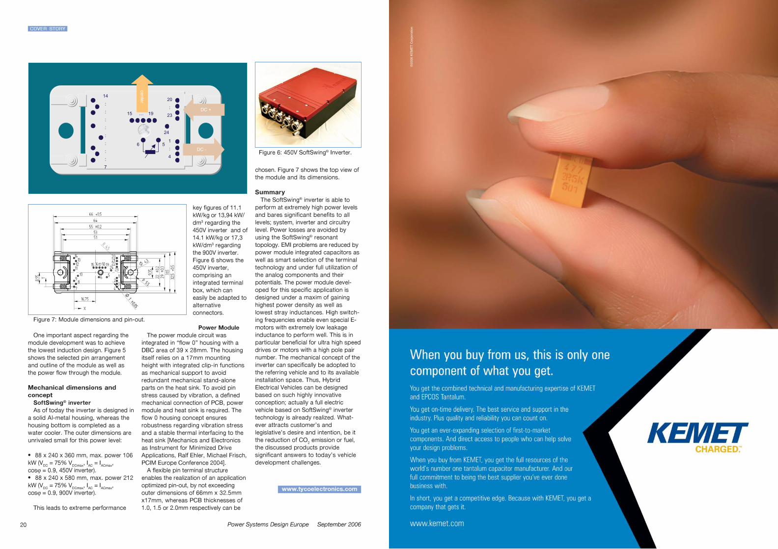
the module and its dimensions.
Summary
The SoftSwing® inverter is able to
perform at extremely high power levels
and bares significant benefits to all
levels; system, inverter and circuitry
level. Power losses are avoided by
using the SoftSwing® resonant
topology. EMI problems are reduced by
power module integrated capacitors as
well as smart selection of the terminal
technology and under full utilization of
the analog components and their
potentials. The power module devel-
oped for this specific application is
designed under a maxim of gaining
highest power density as well as
lowest stray inductances. High switch-
ing frequencies enable even special E-
motors with extremely low leakage
inductance to perform well. This is in
particular beneficial for ultra high speed
drives or motors with a high pole pair
number. The mechanical concept of the
inverter can specifically be adopted to
the referring vehicle and to its available
installation space. Thus, Hybrid
Electrical Vehicles can be designed
based on such highly innovative
conception; actually a full electric
vehicle based on SoftSwing® inverter
technology is already realized. What-
ever attracts customer’s and
legislative’s desire and intention, be it
the reduction of CO2 emission or fuel,
the discussed products provide
significant answers to today’s vehicle
development challenges.
Figure 6: 450V SoftSwing® Inverter.
Figure 7: Module dimensions and pin-out.
www.tycoelectronics.com


Power Systems Design Europe September 200624
AUTOMOTIVE/POWER MOSFETs
While any circuit must operate
over a 9 to 16V nominal
range, other exigencies
include load dump, cold crank, reverse
battery, two-battery jump, spikes, noise
and an extremely wide temperature
range. During load dump, the output
voltage of the alternator surges to 60V
or more. Cold crank, a name that
describes starting the car at low
temperatures, causes the battery
voltage to sag to 6V or less. Reverse
battery is the result of carelessness
with cable polarity when jumping a
dead battery. Many tow trucks are
equipped with two 12V batteries in
series to assist with starting a car with
a dead battery, in cold weather. This
elevates the electrical system to the
28V range, until the car is started and
the tow truck driver disconnects the
jumper cables. Spikes and noise are no
surprise, given that an automotive
electrical system comprises high
current motors, relays, solenoids,
lamps and chattering switch contacts.
Furthermore, the alternator, a 3-phase
machine with chopped field regulation,
at times charges the battery with a very
high current.
A passive protection network for
automotive electronics is shown in
Figure 1. Arrangements identical, or
similar to this one, are widely used to
protect various systems tied to the
automobile’s 12V bus. The network
protects against high voltage spikes,
sustained overvoltage, reverse battery
and excessive current draw. Current
protection is obvious, fuse F1 blows if
the load exceeds 1A for very much time.
D1 and F1 combine to protect against
reverse battery connections; a high
current flows through forward-biased
D1 and blows the fuse. An interesting
property of electrolytic capacitors is
noted at about 150% of the rated
voltage: they draw higher and higher
current as the terminal voltage is
increased, and in the case of C1, it
serves as a clamp (eventually blowing
the fuse) during sustained input surges.
Two-battery jumps at around 28V do
not blow the fuse because the 25V C1
rating is sufficiently high so as to draw
very little excess current. The inductor
adds a small resistance to limit peak
fault current, and to limit the slew rate of
input transients to assist C1’s clamp-
ing action in the presence of spikes.
The primary disadvantage of the
passive network is its reliance on
blowing a fuse for overcurrent,
overvoltage, and reverse battery
protection. Another disadvantage is its
reliance on an electrolytic capacitor for
clamping. As the capacitor ages and
dries out its ESR increases, impairing
the clamping action. Sometimes a
large zener diode is substituted for D1
to assist the capacitor. Active circuits
have been devised to overcome these
deficiencies.
An active solution shown in Figure 2
is designed for shielding sensitive
circuits from the vagaries of a 12V
automotive system. The LT1641 is
used to drive an input n-channel
MOSFET, providing additional protec-
tion not featured by the passive
solution. First, the LT1641 turns off the
load below an input of 9V to prevent
malfunctions at low input voltage, and
to relieve the system from delivering
precious current to non-critical loads
during starting, or when the charging
system fails. Second, the LT1641 soft-
starts the load by gradually ramping
the output when power is first applied.
Third, the output is protected against
overloads and short circuits by current
limiting and a timed circuit breaker. The
circuit breaker auto-retries at a 1-2Hz
rate in the event of a current fault; a
fuse upstream of the protection circuit
can be sized so as never to blow as a
Harsh conditions need special treatmentAutomotive is a brutal environment for electronics. What follows are circuits that are designed
specifically to accommodate operation under these conditions.
By Mitchell Lee, Hua (Walker) Bai & Jeff Witt, Linear Technology
Figure 1. Passive protection network
features simplicity.

Power Systems Design Europe September 200626
AUTOMOTIVE/POWER MOSFETs
result of a current fault downstream of
the LT1641. Finally, the circuit in Figure
2 blocks over-voltages appearing at the
input, while at the same time delivering
a clamped output so that the load
circuitry can continue operating right
through the overvoltage event.
Under normal conditions with a 12V
input, the LT1641 charges the gate to
about 20V to fully enhance the MOSFET
and deliver power to the load. A 27V
zener diode, D1 is connected from the
gate to ground but plays no role in the
9-16V operating range. When the input
rises above 16V, the LT1641 continues
to charge the gate in an attempt to keep
the MOSFET fully on. If the input rises
too far, the zener will clamp the
MOSFET gate and limit the output
voltage to about 24V. The LT1641 itself
can handle up to 100V at the input, and
is unaffected by the clamping action on
the gate. The gate clamp scheme is
certainly more precise than the passive
solution, and is easily adjusted to suit
the requirements of the load by simply
choosing an appropriate breakdown
voltage for D1.
The circuit shown in Figure 2 works
well for loads of up to about 1A, but for
higher load currents the technique
illustrated in Figure 3 is recommended
to prevent over-dissipation in the
MOSFET. Excessive dissipation is a
risk if the overvoltage condition is
sustained, such as when the electrical
system is powered from two series
connected batteries for an extended
period, or even for slow load dump
surges and small MOSFETs. The
output is sampled by D1 and Q2; if the
input exceeds 16.7V, a signal is fed
back to the SENSE pin to regulate the
output at 16.7V. Regulation is more
precise than in the previous circuit
(Figure 1), and is easily customized to
meet the needs of the load by selecting
the appropriate zener.
Total dissipation is limited by the
TIMER pin, which keeps an account of
the total time spent by the MOSFET
regulating the output. If the overvoltage
persists for longer than 15ms, the
LT1641 shuts down and allows the
MOSFET to cool. The circuit attempts
to restart after about half a second.
This cycle continues until
the overvoltage is re-
moved and normal
operation resumes.
Overcurrent faults are
handled in a similar
manner to that described
for Figure 2.
Reverse battery protec-
tion can be added to the
circuits of Figure 2 or 3 by
simply including a series
diode, a conventional p-n
diode in most cases or a
Schottky if forward drop
is important. In critical
applications where the power loss in a
blocking diode is unacceptable, the
simple adjunct shown in Figure 4 will
do the job. Under normal operating
conditions, the body diode of MOSFET
Q2 forward biases and passes power
to the LT1641. When that device turns
on, gate drive is applied to Q2 turning it
on fully. If the input is applied in
reverse, the emitter of Q3 is pulled
below ground and turns on, dragging
the gate of Q2 down and keeping is
close to Q2’s source. In this case Q2 is
held off, and it blocks the reverse input
from reaching the LT1641 and load
circuitry. A microampere-level current of
no consequence flows through the 1M-
ohm resistor to the LT1641’s GATE pin.
Step-down regulators such as the
LT1616 that have maximum input
Figure 2. Overvoltage transient protector clamps output
at ~24V and disconnects if the input drops below 9V.
Figure 3. Regulating clamp clamps input surges and protects
MOSFET against over-dissipation.
Figure 4. Reverse battery protection for Figures 2
and 3.

29www.powersystemsdesign.com
THERMAL CONTROLAUTOMOTIVE/THERMAL CONTROL
Power Systems Design Europe September 200628
THERMAL CONTROLAUTOMOTIVE/THERMAL CONTROL
Thermal design practice for high powerelectrical automotive subsystems
With electrical and electronic systems in today’s vehicles, driving is easy. But these add heat to an
already hot environment. Designers need to cope with this.
By Nico Bruijnis, European Marketing Manager, The Bergquist Company
Major vehicle subsystems such
as power steering, brake
actuators, valve operation
and direct fuel injection are migrating to
electrical and electronic
implementation, delivering savings in
cost, size and weight. But these high-
power electric drives also represent
significant heat sources in locations
close to the engine, brake rotors and
exhaust system, where ambient
temperatures are already high. For
instance, temperatures at the exhaust
system and brake rotors can exceed
500oC, and the surface of the engine
itself can reach more than 200oC.
Even though component suppliers
are qualifying automotive parts up to
175oC, close attention must be paid to
maintaining temperatures within this
maximum to allow continuous opera-
tion at full rated power. Since excessive
temperatures will impair reliability, to
the detriment of safety and market
acceptance, designers of vehicles and
electronic or electrical subsystems
must prioritise thermal management
and cooling of electronics from the
earliest stages of vehicle design.
Processing and Control Modules
Electronic engine control units (ECU)
have been a feature of new vehicle
designs for many years. There has
been a clear trend toward more power-
ful processing capabilities including
digital signal processing for smoother
and more efficient engine operation, as
well as integration of advanced fea-
tures such as variable valvetrain
control. A current, high-end ECU, for
example, may include a 32-bit
processor, DSP, fuel injector outputs,
and several IGBT coil drivers. There is a
clear upward pressure on power
density, with a corresponding increase
in heat dissipation from the module as
a whole. Typically, the ECU is delivered
as a self-contained unit comprising
integrated connectors, and with the die-
cast casing acting as an integral
heatsink.
While an ECU, particularly at the
lower end of the market, may be
mounted in the passenger
compartment, mounting under the
hood (UTH) or directly on the engine
saves significant wiring and allows
faster and more direct control of engine
electrical systems. Thermal design of
the ECU is thus more critical with each
successive generation of module and
vehicle design. The efficiency of the
heatsink-casing, which is influenced by
size, shape and material
characteristics, is critical. So, too, is
the need to create an efficient thermal
pathway between the major heat
dissipating electronic components and
the case.
The thermal characteristics of the
substrate are increasingly important as
designers of automotive electrical
subsystems seek to absorb heat from
power devices included in the
assembly, The substrate must transfer
this heat to the module casing, from
where it can be dissipated into the
surrounding air. Vehicle manufacturers
and subsystem designers are consid-
ering a number of enhanced substrate
technologies. These include Direct
Bonded Copper (DBC), Low Tempera-
ture Co-Fired Ceramic (LTCC), Thick
Film Alumina, Beryllium Oxide (BeO)
and insulated metal substrate (IMS). A
suitable substrate technology,
however, not only displays high
thermal conductivity but must also
deliver high reliability and current
handling as well as supporting flexibil-
ity in mechanical designs.
DBC technology, for example, is
AUTOMOTIVE/POWER MOSFETs
voltage rating of 25V or less are not
generally considered for automotive
applications. Nevertheless, if combined
with a low dropout (LDO) linear regula-
tor such as the LT3012B/LT3013B, the
voltage deficiency is easily overcome.
The small, yet efficient combination
shown in figure 5 provides a 3.3V
output in an automotive environment.
The LT3013B has a wide input voltage
of 4V to 80V with integrated reverse
battery protection, saving cost and
board space without the need for
special voltage limiting or clamping
circuits. The efficiency of an LDO
regulator is nearly VOUT/VIN when
operating with a moderate load current.
If VOUT is much lower than VIN, the
efficiency of an LDO suffers. For
example, step a 12V input down to a
3.3V output results in only 28%
efficiency. Much better efficiency is
achieved in Figure 5 by operating the
LT3013B in dropout over the normal
input voltage range. In this case, the
output voltage of the LT3013B is set to
24V. The output of the LDO will be just
400mV below the VIN, and delivers
power to the LT1616 buck regulator
with 97% efficiency right in the heart of
the normal operating range. During load
dump events, VIN may surge as high as
80V, but the LT3013B will be regulate
and effectively “limit” its output to 24V
for any VIN exceeding 24.4V, well within
the rating of the LT1616 switcher. If VIN
rises above 24.4V, the LDO efficiency
falls, but this condition persists for
only a short time and is of no
consequence. The LT1616 converts the
limited output of the LT3013B to 3.3V.
The switcher efficiency is around 80%
at a 12V input. During cold crank, the
car’s voltage can drop to 5V. Under this
condition, the LT1616 input voltage is
4.6V, well within its range of operation.
Test results of the Figure 5 circuit are
shown in Figures 6 and 7.
The combination of the LT3013B
LDO regulator and the LT1616 switcher
regulates the 3.3V output over a wide
range of operation conditions typical of
an automotive 12V electrical system,
without sacrificing efficiency.
A more integrated solution is the
LT3437 [1]. The LT3437 is a 200KHz
monolithic step-down regulator that
accepts input voltages from 3.3V to
Figure 5. LT3013B serves as a voltage limiter.
80V. Its low quiescent current of
100uA under a no load condition is a
must for today’s always-on systems.
An inexpensive diode can be put in
series with the input to offer reverse
battery protection.
The challenges of the automotive
electrical environment and a traditional
Figure 6. Waveforms of the Figure 5 circuit.
Figure 7. Waveforms of the Figure 5 circuit.
www.linear.com
passive protection circuit are
introduced. Several circuits featuring
LT1641-2, LT3013B/LT1616, and
LT3474 are designed for operation in
an automotive environment.

31www.powersystemsdesign.com
THERMAL CONTROLAUTOMOTIVE/THERMAL CONTROL
Power Systems Design Europe September 200630
THERMAL CONTROLAUTOMOTIVE/THERMAL CONTROL
thermally conductive material signifi-
cantly improves overall thermal
performance. However, selecting the
right gap filling material is critical. For
instance, the required thermal conduc-
tivity of the material is related both to
the thickness of the gap to be filled and
the power rating of the motor. The cost
of the gap filling material also tends to
be greater for high thermal conductivity
formulations, which may require the
designer to choose the optimum
material from a range of alternatives, or
to have a custom gap filler developed.
Bergquist has recently completed
two projects with major European car
manufacturers, in which special gap
pad materials meeting custom thermal
conductivity requirements were
developed. One, to meet the require-
ments of a small car variable speed
cooling fan design, resulted in a gap
pad material displaying thermal
conductivity 1.5 W/m-K while also
meeting the car makers requirements
for resistance to cut-through and other
environmentally-driven requirements. A
similar project for a larger vehicle, on
the other hand, required development of
a special automotive gap pad material
achieving very high thermal conductiv-
ity of 3 W/m-K, reflecting the higher
thermal transfer requirements of the
more powerful motor drive.
The composition and technology
roadmap of gap filling materials are
such that there is a trade-off between
thermal conductivity and cost. Hence,
in a high-volume application such as
an automotive project, subsystem
designers frequently work with
Bergquist to customise a solution that
exactly suits their requirements. On the
other hand, a wide range of off the shelf
gap filling pads, such as Gap-PadTM,
are available in a variety of pre-cut
dimensions including custom shapes
and in a choice of thermal conductivity,
from 0.8 W/m-K to 5.0 W/m-K. Other
gap filling solutions, such as Sil-PadTM
and Hi-FlowTM phase change materials,
are frequently used to ensure efficient
bonding of power MOSFETs to a
heatsink rail and offer additional
benefits such as easy assembly. In
practice, efficiently bonding a power
device to its heatsink allows designers
to operate the device closer to its
maximum rated current or voltage, or
over a greater duty cycle. This offers the
designer opportunities to reduce the
overall component count, thereby
saving size and bill of materials costs,
as well as improving reliability.
Best Practice Thermal Design
In general close attention to thermal
design, and co-operation with materi-
als partners supplying technologies
such as gap filling and thermal sub-
strates to the project, is important to
meet the stringent performance,
reliability and cost targets prevailing in
the automotive environment.
www.bergquistcompany.com
already widely used within the automo-
tive domain, particularly in locations
where temperatures can increase above
180oC. These not only include ECU
positions, but also modules that may
be mounted inside certain major units
such as the gearbox, for example, to
perform transmission control
functions.
On the other hand, a DBC substrate
can be brittle, and the technology does
not provide the flexibility to build
custom shapes. An IMS technology
such as Bergquist Thermal-Clad does
allow designers to specify special
shapes such as circular or half-round
substrates, to utilise space within the
engine compartment and other areas of
the vehicle more efficiently. IMS also
offers the advantage that it can be
shaped in 3-dimensional formats for
greater design flexibility and shows
higher mechanical stability than most
ceramic or bonded substrate
technologies. As an IMS technology,
Thermal-Clad also allows customers a
choice of base layer materials, includ-
ing aluminium or copper, and a choice
of thicknesses to further extend control
over thermal conductivity, thermal
capacity and the overall size and
volume of the assembly. The electrical
isolation and thermal impedance
properties of IMS are governed by the
characteristics of the dielectric layer
residing between the electrical intercon-
nect layers and the base material. The
dielectric combines a polymer material
that determines electrical isolation,
stability throughout thermal ageing,
and bond strength, with a ceramic filler
to enhance thermal conductivity and
maintain high dielectric strength. The
composition of the dielectric is ad-
justed to emphasise one or more
characteristic, such as high thermal
conductivity, to match the requirements
of a given set of applications. There is
a choice of four dielectrics for use with
Thermal-Clad, which allows customers
to specify an optimal composition in
terms of performance and cost.
Another valuable aspect is that,
whereas IMS has traditionally been
viewed as a single-layer interconnect,
Thermal-Clad technology supports
two-layers of interconnect.
Motors and Drives
Successful operation of electrical
systems such as EPS, electro-me-
chanical braking, electrical valve
operation and variable speed cooling
fans depend on efficient, lightweight
electric motors. In these situations,
electronic controls deliver the desired
controllability, are smooth in operation,
and are cost-effective. These motor
controllers are now distributed at many
locations throughout a modern vehicle,
and must be designed not only to
dissipate the heat generated internally
by processing and power switching but
also to include protection from the heat
generated by the motor. This is becom-
ing increasingly important as these
controllers are now migrating into the
motor assembly itself, as part of the
trend toward mechatronic solutions.
Among high power automotive
electrical subsystems, Electrical Power
Steering (EPS), is an attractive goal for
car makers. EPS offers savings in cost,
weight and fuel consumption com-
pared to conventional hydraulic
solutions. Some current models
already have full EPS, and most car
makers have a roadmap to implement
this technology. The required motor
output depends on the size and weight
of the vehicle, and may range from
300W to around 800W or more.
Conduction and switching losses in
the MOSFETs of the motor driver,
particularly during heavy use of the
steering system such as when parking,
are dissipated as heat. Again, a large
die-cast heatsink is usually used. In
the case of EPS, the MOSFET
assembly, as well as the electronic
control unit if fitted, may be integrated
into the motor itself.
Engine cooling fans, on the other
hand, benefit from variable speed
operation to support a more flexible
engine cooling strategy and also
enable better management of the
overall vehicle electrical budget. Speed
control is a key advantage of electronic
motor controls, but the driver switching
the motor drive current must be able to
dissipate losses in proportion to the
power of the fan motor. For a small
vehicle, this power may be in the range
300-500 Watts. For a larger car, on the
other hand, a motor of 800-1000 W
may be necessary.
These high power systems require an
efficient thermal path from the transis-
tor casing to the heatsink. Air gaps are
the greatest enemy in this respect,
since the thermal conductivity of still
air is very low at 0.0262 W/m-K. This
compares with 400 W/m-K for copper:
clearly, even a thin air gap between two
metallic surfaces will dramatically
increase the overall resistivity of the
thermal path to ambient. Since air gaps
are inevitable where a component
attaches too a heat sink or other
surfaces, filling these gaps with a

33www.powersystemsdesign.comPower Systems Design Europe September 200632
AUTOMOTIVE/POWER MANAGEMENT AUTOMOTIVE/POWER MANAGEMENT
low voltage difference between input
and output voltage, using a linear
regulator could be the best solution.
The linear regulator ICs are less
complex than switching regulators so
they need less power themselves. The
overall power loss in a
linear regulator consists
of three main parts:
1. The power path
losses which consist of
the voltage difference
between the output and
input voltage times the
load current.
2. The power used to
support the functions of
the linear regulator. The
classic quiescent
current. Given in the
datasheet of the IC.
3.The power lost in the
feedback resistors.
Dependent on the value
of the feedback resistors
and the output voltage.
National Semiconductor’s LM2936 is
a linear regulator optimized for low
quiescent current. Its quiescent current
is dependent on output load and at
output currents of 100uA the quiescentT
he biggest trend in power sup
plies over the years has been to
maximize efficiency within the
monetary budget available to power
supply designer. Besides this goal
there are of course other optimization
parameters like dynamic response,
noise behavior or optimized failure
behavior. One particular requirement
has become of great importance
recently particularly from the automo-
tive industry: low quiescent current.
Long battery life is important and
depends on the efficiency of the power
supply at a given load. If we do not
have the possibility to change the load
we can only boost the efficiency of the
power supply. One way to increase the
efficiency especially at low output
loads is to decrease the quiescent
current of the power regulator IC.
Quiescent current is the current that a
certain power supply consumes when
turned on but no output power is
drawn. In shutdown condition most
modern power supplies only consume
a few uAs of current. But as soon as
little load on the output is attached the
power supply has to operate and will
consume power. This Power has two
main causes. (Figure 1) One is the input
voltage times the current that the power
regulator IC draws when turned on.
This current is used to power internal
devices such as the precision reference,
the PWM generator the oscillator as
well as the Error Amplifier and many
more blocks that have to be powered in
steady state operation. The second
source of the consumed power comes
from the feedback resistors which are
used to set the output voltage. Here the
power results from the adjusted output
voltage and the total resistance of
RFB1 and RFB2. Voltage square
divided by the Resistance. So the
higher the resistance of the feedback
resistors the less power is consumed.
This optimization has
certain limits in reality. If
the resistance gets to
high, noise can easily be
coupled on to the FB pin
of the power IC. This noise
can cause problems in the
regulation loop. A practical
upper resistance value is a
few hundred kilo ohms. If
a power IC with a fixed
output voltage without
external feedback resistors is used, it
does not mean that this power loss is
non existent. In reality the feedback
resistors are just well matched internal
resistors. Often the adjustable version
of power ICs with external resistors
offer more flexibility in selecting the
feedback resistors and by this offer a
better way in controlling the current
lost. On the other hand internal resis-
tive dividers offer optimized resis-
tances and less susceptibility to noise
since the high impedance node at the
error amplifier is not pined out.
New requirements in automotive
A rather new development in market
requirement came with the soaring
electronic content in the automobile.
Obviously, the more systems a car
battery has to supply power to, the
quicker it will be discharge. Once the
combustion engine of the car is running
and the battery is charging there is not
such a big problem. As soon as the car
is turned of, but some systems still
require constant power we can run into a
problem when the car battery is dis-
charged after the vehicle has not been
driven for a few weeks or even days.
Systems that need constant power are
real time clocks, memories, alarm
systems including sensors and alike.
A linear regulator approach
For many applications, especially
with small output currents as well as
How very low quiescent current step down ICconverters offer solutions to difficult problems
When you park the car, the battery is still supplying power to certain systems. How can we
design to avoid a lock-out upon our return?
By Michele Sclocchi and Frederik Dostal, National Semiconductor
Figure 2. LDO quiescent current vs. output current.
Figure 1. LDO quiescent current.
current is less then 20uA. (Figure 2)
The power path losses are very small
if the output current is very small. So in
many cases using a linear regulator for
efficient power conversion at low
output load is a very good solution.
A switching regulator approach
Switching regulators generally need
much more quiescent current due to the
higher complexity of the regulator ICs.
Also a switching regulator has to
recharge the switching element (usually
a MOS FET) every time the switch is
turned on. If a certain regulator is
switching at a constant frequency the
total efficiency at very low output loads
is very low. Systems that need high
efficiency at low loads as well as the
capability to provide high loads often
use two parallel power supplies. (Figure
3) One switching regulator to provide
high efficiency at high loads and then
at low loads the switching regulator is
turned off and a low quiescent current
LDO is taking over. Such a system

35www.powersystemsdesign.com
AUTOMOTIVE/POWER SEMICONDUCTOR DESIGN
Power Systems Design Europe September 200634
AUTOMOTIVE/POWER SEMICONDUCTOR DESIGN
Many industry sources are
predicting continuing in
creases in the market for
semiconductors in automotive
applications. In last year’s Power
Systems Design Europe automotive
supplement Chris Ambarian suggested
$23bn by 2009 with power electronics
making up 12 to 13% of this. In 2004
Derek Lidow indicated that the expected
compound annual grown rate (CAGR)
would be 8.3%. With such figures, and
the added benefit of longer term
stability, automotive electronics can be
a very attractive prospect.
However, any component supplier
contemplating entering this market
should be fully aware of the wide
ranging demands that will be placed on
them. These vary from broad commer-
cial to detailed technical requirements,
including significant delayed return on
investment due to extensive automo-
tive qualification requirements, medium
level volumes when in production and
intense expectation of continuous
improvement in quality and price over
the lifetime of the product.
Electrical Requirements
In most applications, power electron-
ics will be connected directly to the
main vehicle power network. For cars
this is nominally 12V but can be as low
as 5V during cold engine starting and
as high as 24V during double battery
starting. It can also exceed 40V during
a “load dump” condition if the battery
becomes disconnected from the
alternator. In addition the many induc-
tive loads, and the inductance of the
wiring harness itself during load
switching, can inject severe distur-
bances on the power network. All
electronics connected directly to the
power network must be capable of
surviving these transient conditions.
ISO7637 defines the basic require-
ments for these electrical disturbances
and includes five basic test pulses with
recommended duration varying from a
few microseconds to a few seconds
and recommended test voltages up to
150V. Each of the major car manufac-
In addition to the specific functional requirements of any component designed for automotive
applications, three key technical areas need to be considered in detail:
Electrical, Environmental and Reliability.
By Bob Christie, European Applications Manager, Allegro Microsystems
Figure 1. Protecting Low Voltage Components.
AUTOMOTIVE/POWER MANAGEMENT
works well but requires two indepen-
dent power supplies, relatively complex
control mechanisms and a large bill of
material.
New switching regulators such as
National Semiconductor’s LM26001
combine such a complex solution into
one easy design. The LM26001 only
Figure 3. Two parallel power supplies.
consumes a
typical 40uA
while providing
loads of a few
hundred uAs of
load current.
Such a quies-
cent current
optimized
design operates
in a pulse skip
mode so that
energy is only
shuffled from
the input to the
output if really
needed. This
way charging
losses of the switching element can be
optimized. The LM26001 can deliver up
to 1.5A of continuous load current with
a fixed current limit, through the
internal N-channel switch. The part has
a wide input voltage range of 4.0V to
38V and can operate with input volt-
ages as low as 3V during line
transients.
www.national.com
The quiescent current is down
With new switching regulators
coming to the market like the LM26001
it is possible to support many low
quiescent current applications to
provide a very well tailored solution.
Low quiescent current applications are
here to stay so expect more develop-
ment in this field resulting in a larger
selection of semiconductor products
coming up.
37www.powersystemsdesign.com
AUTOMOTIVE/POWER SEMICONDUCTOR DESIGN
Power Systems Design Europe September 200636
AUTOMOTIVE/POWER SEMICONDUCTOR DESIGN
turers has their own set of standards
based on this ISO standard. Some
manufacturers demand load dump
capability up to 60V and all include a
reverse battery requirement where the
equipment must survive a battery being
connected the wrong way round in
error.
Operating and surviving these
voltage requirements requires a
combination of system and compo-
nent design techniques and special
processes. An example of such a
process is the Allegro ABCD4
process used in a number of auto-
motive MOSFET gate drivers and
supply controllers. This process
combines small geometry low
voltage elements, for design of logic
sections, with medium and high
voltage components for direct
connection to the power network and
discrete power devices. The process
has been specifically designed to
withstand the transient voltages
seen when driving brush and
brushless DC motors and has is well
suited to the automotive electrical
environment.
When the use of complex compo-
nents is required, such as
microcontrollers and DSPs, or delicate
components such as high power
LEDs, then these must be protected by
additional circuits. Fig.1 shows an
example of a high performance
microcontroller system with sensors,
which may require several low voltage
supplies. 1.8V for the core, 3.3V for the
I/O and 5V for the sensors and analog
interface. These can be provided by a
single automotive switching regulator
with multiple linear regulators such as
the Allegro A8450. This multiple
output regulator is capable of operat-
ing from 6V to 45V and provides a
protecting interface between the
sensitive components and the auto-
motive power net.
As with all electronic components,
ESD and EMC are other major
considerations. Any component that is
connected directly to the wiring harness
of the vehicle will usually have to
survive 4kV discharges based on the
human body model (hbm). In many
cases this is increased to 8kV and
sometimes even higher at 15kV.
Components that are not connected to
the wiring harness usually have to be
capable of withstanding at least 2kV
hbm discharges. At higher frequencies
each manufacturer defines their own
EMC requirements based on CISPR25
and ISO11452.
Environmental Requirements
Power electronics are generally used
to control some form of mechanical
actuator. If the actuator is in the engine
compartment then the control electron-
ics are increasingly mounted close to
or, in many applications, inside the
body of the actuator. In this case the
power semiconductors must be
capable of operating at ambient
temperatures down to -40oC and up to
150oC in some applications.
Provided the component has been
designed to operate at low
temperatures, inexpensive plastic
packages do not usually present a
problem. The main design challenge,
for circuit and package, is at high
temperatures. Not only will the load
and the engine itself be generating
heat, raising the ambient temperature
but the power electronics will also
dissipate power in the form of heat.
The circuit challenge at high tempera-
ture is to maintain the performance of
the controller. The packaging challenge
is to remove the internally generated
heat from the components and keep
the temperature difference between
ambient and silicon junction at an
acceptable level.
Except in a few cases, packages
based on special low thermal resis-
tance materials and assembly tech-
niques would be too expensive. Instead
the cost and performance requirements
can be met using a combination of
design techniques to reduce power
dissipation and new, near-chip-scale,
plastic packages with exposed tabs (e)
for heat conduction. For example, fig 2a
shows the internal structure of a small
2mm x 3mm eMLP package and fig 2b
shows the heat profile in the package
when dissipating 1W. Larger pin count
MLP packages, miniature quad flat
pack and TSSOP packages are all
available with exposed pads and
provide a cost effective solution to
automotive packaging for components
such as FET gate drivers and power
supply controllers.
Figure 2a. 3x2 eMLP construction. Figure 2b. 3x2 eMLP heat conduction.

39www.powersystemsdesign.com
AUTOMOTIVE/LCDs
Power Systems Design Europe September 200638
AUTOMOTIVE/LCDs
Explosive growth in liquid crystal
display applications continues
to exceed expectations. Prior
beliefs of many analysts and industry
participants, for instance, that liquid
crystal display (LCD) televisions would
have relatively slow adoption and
remain a smaller sibling of plasma TVs
have been drastically revised.
On a smaller scale, many simple
monochrome information displays have
been replaced with impressive, true thin-
film transistor (TFT) LCDs in applica-
tions such as automotive or communi-
cations handsets, where cost once was
perceived to be a major barrier. These
new applications highlight a number of
issues and pose new requirements for
the display system designer.
The main points of this discussion
center on issues which we can relate to,
as electronics consumers, in the year
2006. This article will focus on display
ergonomics, comfort, and in some
cases safety.
As system designers might note, for
each of these benefits there are a
number of complimentary technical by-
products relating to battery life, lamp
life, power savings and others. Most
consumers targeted in television
advertisements and by “high tech”
electronic gadget stores are unaware of
these technical issues and their
impact. They do however experience a
cell phone that is far too bright in a
dark night time situation, or a nearly
illegible digital camera display in a
bright daytime environment.
The aspects of LCD design that will
be discussed are as follows:� Overall display brightness range.� Ways to take advantage of
brightness range and its associated
benefits via “Automatic Brightness
Control” (ABC).� Simple do’s and don’ts regarding
an “autobrite” display implementation.
One of the most critical design
criteria in display backlighting is to
ensure that the brightness capability
range matches the needs of the end
product. For example, an LCD TV
typically operates in a less dynamic
ambient light environment than a
hand-held device, such as a cell phone.
This dictates that the hand-held
display should have a greater overall
brightness range capability than a
product designed to operate in a
constant or “controllable” environment.
Despite this intuitive understanding,
brightness range is a commonly
overlooked aspect in the design of
portable display products. Many
digital cameras and various handsets
are designed to be legible in a specific
“mid level” ambient brightness
condition. Operation outside of these
conditions can be extremely
frustrating, as when attempting to
shoot a digital photo at night, or to
read a cell phone display in bright
daylight. Both of these situations are
unacceptable for most consumers –
and can be resolved quite easily.
The low ambient light solution simply
requires designing a display backlight
with a wider dimming range, hence
providing a lower brightness operating
mode. This minor adjustment in-
creases user satisfaction – allowing
photographers, for example, to glance
back and forth from subject to display
without requiring frequent adjustments
of their pupils.
The desired operation in a bright
environment is a little more difficult to
provide. This requires additional
backlighting (lux or nits) capability to
be designed into the product in order
for the display to compete success-
Ambient light affects readability of LCDdisplays
Poor readability can be annoying. In a critical application, dangerous.
By Roger Holliday, Vice President, Microsemi Integrated Products Group
AUTOMOTIVE/POWER SEMICONDUCTOR DESIGN
Low on-resistance n-channel
MOSFETs can be used to help reduce
power dissipation in the controller but
only if they are provided with sufficient
gate drive under all conditions. The
allegro A3946 (fig.3) is an example of a
simple half bridge driver with a number
of features to ensure that the
MOSFETs are always driven at the
optimum level. A high-side drive, a low
side-drive and associated power
supply management and diagnostic
circuits are all included. The high-side
drive uses a bootstrap capacitor to
provide the above supply voltage
required to keep the high-side n-
channel MOSFET active.
A regulating charge pump maintains
a sufficiently high gate drive voltage
during low supply voltage conditions
to ensure full conduction in the
MOSFET and limits the gate drive
voltage at high supply voltage to
prevent damage to the MOSFET. The
A3946 contains several additional
ease-of-use features such as auto-
matic bootstrap charge management,
system and MOSFET diagnostics, and
an additional charge pump to maintain
full charge in the gate of the MOSFET
under DC conditions. Similar features
can also be found on the A3940 Full-
Bridge gate driver and the A3930 and
A3935 three phase gate drivers.
Reliability
Reliability is probably the most
important part of the technical require-
ment set – and the only part that cannot
be guaranteed by design or test. A key
differentiation between automotive
components and commercial compo-
nents in use is the high ambient
temperatures. The Automotive Electron-
ics Council (AEC) has classified ICs
according to their ability to operate and
survive these high temperatures. Many
power ICs today are rated as grade 1
components able to operate in ambient
temperatures up to +125oC. With the
trend to locate the power electronics in
the body of the actuator, these ambient
temperatures in many instances exceed
the +125oC grade 1 requirement forcing
suppliers to push power IC technology
towards meeting grade 0 (Ta <= 150oC)
requirements. The end goal of course is
to always try to increase the confidence
that, during the lifetime of the vehicle,
any component will achieve a failure
rate as close to zero as possible.
In the first instance, all components
undergo full production testing, usually
at the extremes of the temperature
range, and achieve in excess of 99%
fault coverage. In addition, particularly
Figure 3. A3946 Half-Bridge gate Driver.
for analog and power components, the
test limits are tightened and adjusted
based on the average test results over
a number of batches (part average
testing). This helps remove individual
components which are within the
specified limits but are outwith the
normal distribution of results. In
practise this results in a very low
failure rate when the components are
first assembled into systems.
For lifetime reliability we have to rely
on accelerated life testing of a sample
of products. For automotive products
the Q series of specifications from the
AEC define the required sample sizes
and test conditions that have to
applied. The extreme conditions of
temperature humidity and bias that
are applied are used to accelerate any
possible fault conditions. This allows
a statistical estimate of the mean
time to failure (MTTF) which, for
automotive power semiconductors, is
usually in excess of 50 million hours
or 6,000 years!
Conclusion
The three topics discussed here
demonstrate that supplying power
semiconductor components to the
automotive market is indeed a major
undertaking and not something that
can be approached without major
financial and technical analysis. Start
of production can easily extend to
greater than two years from start of
design to initial sales revenue and
positive cash flow. Once in production
the annual volume of any product may
be from a few hundred thousand for
complex controllers to a few million for
discrete active components. Quality
must be maintained or improved
during the product lifetime and cost is
always a topic for discussion. On the
positive side, once a component is
qualified and in production, provided
the product quality is maintained, it
can enjoy several years of consistent
volume shipments providing stability
to the component supplier.
www.allegromicro.com

41www.powersystemsdesign.com
AUTOMOTIVE/LCDs
Power Systems Design Europe September 200640
AUTOMOTIVE/LCDs
minimize the continual adjustments
made by the human eye when it shifts
its focus on and off the display. This
focusing adjustment process slows as
we age, becoming a potential safety
concern for a number of display-based
products – especially pertaining to
vehicular applications or applications
involving non-continuous use. Non-
continuous use refers to applications
where the user frequently looks both at,
and then away from, the display in a
repetitive fashion. (Unlike a continuous
use TV or computer screen.) In many
such applications, automatic bright-
ness control can reduce product
liability and thus is viewed as extremely
attractive to the manufacturers.
The final point of interest in auto-
matic brightness control is its potential
for creating a more environmentally
friendly or “green” product. The industry
is all too familiar with the regulatory
and compliance conditions we encoun-
ter on a day to day basis. As the
volume of LCD products continue to
increase, we can envision hundreds of
millions of multi-lamp, high wattage,
LCD monitors and televisions in
operation at any give time. In this
environment, interest will be high for
system design concepts capable of
achieving power savings as high as 50
percent under certain conditions. An
example of this is when sleep modes
were incorporated into PCs, in order to
achieve “green” status. There is no
necessity to run an LCD television in
your family room during movie night, at
the same brightness level needed for
airport flight status monitors operating
in a brightly lit airport.
Of course, any discussion of imple-
menting automatic brightness control,
is meaningful only if the performance
and cost criteria objectives can be
met. The key is a new generation of
optical sensors capable of providing
high performance, low-cost, imple-
mentations of automatic display
brightness modes. Of critical
importance, these new sensors have
the ability to detect and respond to
light wavelengths that correlate very
closely to the response characteristics
of the human eye itself. These sensors
eliminate several problems encoun-
tered with prior technology.
Because earlier sensors were
extremely susceptible to infrared and
ultraviolet light they often provided
false readings, based upon these non-
visible light sources. The result was
unusual, and unpredictable, brightness
adjustments at the system level as the
displays adjusted to unseen infrared
or ultraviolet characteristics originated
from such sources as the sun, incan-
descent light bulbs, fluorescent lamps
and even heat. Thus poorly designed
systems would set up an erroneous
display brightness based on high UV
and IR content.
In addition to the improved spectral
response, these new silicon sensors
such as the Microsemi LX1972 (Fig. 2)
also offer extremely good temperature
stability. This is essential as most cold
cathode fluorescent lamps (CCFLs) or
light emitting diode(LED) backlit
displays experience substantial
temperature swings as they operate.
Poor temperature response will result
in changes in display brightness based
on temperature and not light
conditions. A light
sensor should not
be a “thermostat.”
In respect to the
issue of cost/
performance, it is
important to note
that a complete
LCD automatic
brightness control
system, as
described, can be
implemented for
less than one U.S.
dollar. This design
requires no optical
filters, can be user
adjustable and
includes both the
light sensor and all
supporting discrete
components.
Conclusion:
As engineers, we
need to design
systems that have
brightness ranges
capable of operat-
ing in the environ-
ments in which
www.microsemi.com
they are intended to be used. Display
systems with a fixed brightness level
are as logical as an audio system with
only a preset, fixed, volume level. They
are not acceptable from either an
engineering or user standpoint.
The second point is that these
backlighting schemes need to be low
cost and simple to encourage wide
use – since we know that in many
applications the correct display
brightness range and its benefits will
only be realized if its control is
automatic. If this concept is widely
adopted, it has the potential to enable
huge electrical power savings from the
proliferation of display devices
throughout the world. Not to mention
that it also will ensure that when you
turn on your camera, notebook or
phone, it will boot up at a comfortable,
optimal efficiency brightness level
regardless of the operating environ-
ment – and stay that way.
Figure 2. Simple circuitry can provide complete automatic brightness control
modes. In this application, an LX1800 integrated circuit has been added for
additional digital microprocessor control. Brightness levels automatically adapt
to changing automotive ambient environments.
fully with bright ambient light. This
bright condition also affects the light
sensitivity of the human eye, and
raises the problem of additional power
consumption needed to operate in this
“hi bright” manner.
High power burn can be offset by a
contrasting period of low power, low
brightness backlight operation in most
hand-held displays. This diligence in
reclaiming battery life is much like
improving gas mileage by taking
advantage of the downhill coast, after
driving a steep uphill grade. For it to
work, however, users must make
appropriate adjustments to their
displays to match the ambient
conditions. This leads to the subject of
Automatic Brightness Control.
Industry data and research per-
formed by display product manufactur-
ers reveals that the majority of the
product users, do not, or will not, make
significant efforts in adjusting display
brightness. This can be substantiated
by looking at the day to day use of your
own cell phone, notebook PC, or
personal digital assistant (PDA).
Most consumers can’t even recall
how to change the brightness level – or
find that changing display brightness
takes more time than is warranted for
such simple viewing needs s retrieving
an appointment or phone number, or
dialing a phone number. These trans-
actions are short, so it just doesn’t
make sense to fiddle with manual
brightness adjustments. Repetitive,
short-duration use is normal for many
display systems. Fig. 1 shows an
example of the latest sensor
technology’s response profiles as
compared to those of the human eye.
In addition, a lack of interest in
changing display brightness is sup-
ported by the excellent design of the
human eye – with its ability to adjust
its aperture to block or receive addi-
tional light for viewing comfort as
necessary. Since the eye isn’t con-
cerned with saving battery power, it
allows you to leave the display at a
constant brightness by making the
adjustments within the eye instead.
The only way to take advantage of all
the benefits achieved with variable
display brightness is to automate the
adjustment process. Simply remove
the responsibility from the user to
ensure that display brightness always
corresponds to the ambient light. The
many benefits include extending
battery operation, system heat
reduction, and the potential for ex-
tended lamp life.
Two other benefits can justify
automatic brightness control. First, by
getting a close match between display
brightness and its environment, you
Figure 1. Sensor response is approaching human-eye capabilities, a critical
factor for controlling display brightness characteristics.

43www.powersystemsdesign.com
AUTOMOTIVE/SENSORS
Power Systems Design Europe September 200642
AUTOMOTIVE/SENSORS
ground plane between the supply’s
ground and the load to be measured
(See Figure 2). The resulting propor-
tional voltage developed across that
resistance can be used directly or
amplified. One consequence of placing
resistance in the ground plane is that
any voltage signal that crosses the
shunt resistor (Rs) will have an offset
relative to ground, the negative rail is
now at the potential of Vshunt, which
will change with the load current. This
will be unacceptable with most analog
signals. An important property of the
current measurement circuitry is that it
should be able to accept Vshunt, a
signal of typically tens of millivolts
from ground. This issue can be mini-
mized by using an input offset.
In some applications, the loss of true
ground cannot be tolerated because of
the inter-circuit offsets created, as
already outlined. Sometimes, regard-
less of whether the effects of disrupting
the ground plane could be ignored or
tolerated, it is not possible to adopt
this method. Where a system uses a
common ground in the form of a metal
chassis, as found in the automotive
environment, components that are
connected mechanically to it may not
have the first method as an option. It is
then necessary to measure the current
in the supply (high-side).
Dedicated High Side Monitors
The INA19x and INA27x family from
Texas Instruments with voltage output
can sense drops across shunts at wide
common-mode voltages from – 16V to
+80V, independent of the supply
voltage. This wide common-mode
range is ideal for withstanding auto-
motive fault conditions ranging from
12V battery reversal up to +80V
transients, since no additional protec-
tive components are needed up to
those levels. This enables the INA19x
and INA27x to be used in a variety of
automotive applications.
When the common-mode voltage is
positive, amplifier A2 is active, and the
circuit will convert the differential
voltage ((VIN+) – (VIN-)) measured across
the shunt resistor Rs into an output
current (IO) which is then converted back
into a ground referenced voltage
through RL. VIN is impressed across the
internal 5k resistor which in turn
results in a current VIN /5k To maintain
a stable feedback condition, where the
two input terminals of the op amp are
maintained at the same voltage, the op
amp’s output must bias the output
transistor so as to draw this current
out of the node, and pass it down to RL
where it is converted back to a voltage
and then amplified by the built-in
output buffer.
Figure 2. Schematic of Differential High and Low side drivers.
Figure 3. Schematic of INA19x family.
Examples of these developments
include:
1) Automatic transmission, where
electronic control of the hydraulics in
the electromechanical system is
executed by linear solenoids that vary
the hydraulic pressure applied to the
actuators attached to the clutch packs.
2) Automatic window lifter, where the
current flowing during the motor control
of a window lifter is monitored so as to
detect a motor stall which could take
huge currents and destroy the motor-
controlling MOSFETs very quickly.
The figure below shows a simplified
diagram of using a current monitor
during Motor control.
Current is thus an important indica-
tion of a solenoid’s state. The most
effective method of measuring a
solenoid’s current is to measure the
voltage across a resistive shunt con-
nected in series with the solenoid,
battery and switch. There are several
different ways to configure this circuit
for switching and voltage measurement.
Low-Side vs. High-Side
Measurement
Low-side (negative or ground
potential) measuring circuits generally
offer the simplest solutions because
the resulting signal is already ground
referenced. One method to achieve this
is to insert a small resistance into the
Current monitoring in automotiveapplications protects the auto as well as the
occupantsWith the uptake of electronics in the automotive industry to provide more comfort, safety, reliability
and information to the end user, sensors are used in key applications for monitoring purposes.
By John Constantopoulos, Business Development Engineer, Texas Instruments GmbH
Figure 1. Simplified Block Diagram of Current Measurement for Motor Control.
45www.powersystemsdesign.com
NEW PRODUCTS
Power Systems Design Europe September 200644
NEW PRODUCTS
Octal high-side driver provides simplified control of
automotive loads
AMI Semiconductor (AMIS) has
expanded its family of ASSPs
(application specific standard
products) with a new high-side driver IC
to simplify the control of transistor
gates, relays, valves, solenoids, LEDs
and other loads in 12V automotive
environments.
The AMIS-39100 is a highly inte-
grated driver IC, with eight high side
(HS) output drivers and a range of
functions and features designed to
significantly reduce component count
and cost.
Each of the eight output drivers can
drive a continuous current of 275mA
when connected to an inductive load of
300mH. Higher individual output cur-
rents are achievable by limiting device
current to the total maximum. The drivers
will withstand short circuits to the battery
or to ground, even in situations where the
device itself has lost its ground
connection. The drivers also provide
over-current limiting and shut-down in
the case of a fault condition. Additionally
an integrated charge pump and over-
temperature protection circuit avoids the
possibility of thermal runaway, even at
low battery voltages.
Compatible with 3.3V and 5V
microcontrollers, the SPI interface is
used to control each of the individual
output drivers and to provide a route for
the integrated diagnostic circuit to
feedback error signals. The interface
can also be used to read back the
status of the built-in thermal shutdown
protection function.
“Automotive designers are demand-
ing actuator and controller solutions
that help them simplify and accelerate
application development,” says Tony
Denayer, AMI Semiconductor’s senior
vice president, high voltage communi-
cations and ASSPs. “The high level of
integration addresses this demand,
and complements our existing range of
standard components for driving and
controlling motors and loads in
automotive applications.”
The AMIS-39100 incorporates a
power-down mode during non-active
periods and an integrated slope control
function minimizing electromagnetic
emission (EME). Operating temperature
is rated at -40oC and 105oC and the
device is supplied in a compact SO28
package.
www.amis.com
Fastest transient response with highest system accuracy for computing power management
Intersil has introduced a family of
four-phase synchronous PWM (pulse
width modulation) buck controllers
claimed to deliver highest performance/
price ratio for four-phase CPU core
regulators. Intel VR10/11 and AMD AM2
CPU core solutions using these
controllers need many fewer bulk
output capacitors. The devices feature
Intersil’s active pulse positioning
(APPTM) and adaptive phase alignment
(APATM) modulation schemes.
Nominated ISL6312, ISL6312A and
ISL6322, these devices provide an
integrated precision voltage regulation
system for advanced Intel VR10/11(Intel
Core 2 Duo and Intel Core 2 Extreme)
and AMD AM2 5/6-bit microprocessors.
The family features programmable VID
(voltage identification) codes for Intel
and AMD DAC (digital-to-analogue
converter) tables.
Family variations are available for
many popular computing applications
to enable customers to monitor the
CPU load current in real-time and to
work with overclocking applications
such as performance motherboards
using Intel’s Core 2 Extreme processor.
All three device types incorporate a
unity gain differential amplifier for
remote voltage sensing that compen-
sate for differences between remote and
local grounds and also integrate three
MOSFET drivers and a PWM output for
a fourth external MOSFET driver.
The ISL6312, ISL6312A and ISL6322
provide advanced control loop features
to optimize transient response to load-
apply and removal functions. These
include accurate and differential con-
tinuous DCR (DC resistance) current
sensing for load line programming and
channel current balance and also ensure
individual channel current and average
overcurrent protection (OCP).
The ISL6312A incorporates an added
IOUT pin to the basic ISL6312 for
output current measurement while the
ISL6322 provides an I2C bus input for
adjusting four basic regulator functions,
such as output voltage, overvoltage
protection (OVP) level, operating fre-
quency per phase, and MOSFET driver
adaptive dead time control. All devices
include open circuit protection on the
remote sensing inputs.
Typical target applications are
desktops, workstations, servers, single
board motherboards, industrial PC
motherboards, routers and switches,
and voltage regulator modules.
Available in 48-lead, 7 x 7 QFN
packaging.
www.intersil.com
AUTOMOTIVE/SENSORS
accuracy at lower currents by minimiz-
ing the effects of offset, while low
values of RS minimize voltage loss in
the supply line. For most applications,
best performance is attained with an RS
value that provides a full-scale shunt
voltage range of 50 mV to 100 mV.
Maximum input voltage for accurate
measurements is 500 mV.
Conclusion
Current sense monitors serve a vital
role in a wide range of automotive
control systems. They can be used to
provide information on the current,
position, speed and direction of a
rotating motor. In addition, sensors
improve the reliability of a system by
detecting fault conditions that would
damage or destroy a specific
application. The INA19x and INA27x
high side current-sense amplifiers
simplify designs in the automotive
environment. Both the INA19x and
INA27x are available in SOT23 and SO-
8 packages respectively and are
specified for the -40oC to +125oC
temperature range.
Note: The INA27X is scheduled for
release 1Q07.
When the common-
mode voltage is negative,
amplifier A1 is active. The
differential input voltage,
(VIN+) – (VIN-) applied across
RS, is converted to a
current through a 5k
resistor. This current is
sourced from a precision
current mirror whose
output is directed into RL
converting the signal back
into a voltage and ampli-
fied by the output buffer
amplifier. The relationship
between load current and
the resulting voltage (Vout)
can be expressed as:
The main demands
placed on the op amp are
that it may have an offset
voltage significantly lower
than the magnitudes of VIN being
measured, and that its input common-
mode range extends to VIN+. An output
range that comes to within a diode
drop of ground is also necessary.
These requirements are all met by
using an op amp with rail-to-rail I/O.
As an example, consider the implemen-
tation of a 0A to 1A current sensing
application using this circuit and a 20
m shunt resistor. In this case one
would like an output voltage range of
0V to 2V to correspond to the input
range. By setting VOUT= 2.0V, RS= 0.02 ,
and IL= 1A one can solve for the ratio of
RL/1k .
A gain of 50 can also be set if the
shunt resistor is chosen to be 40m .
This provides the designer with more
flexibility, as the gain is dependent on
only one resistor.
Filtering Option of the INA27x
Current measuring is often noisy in
automotive and many other
applications. It may therefore be
necessary to filter the signal to remove
any spurious high frequency transients
that may occur in many applications,
or to extract the mean value of a
fluctuating signal with a peak-to-
average ratio greater than unity. Low-
pass filters can be implemented in
several ways using the features
provided by the INA27x family, and still
preserve the buffered output of the 1st
stage. It readily enables the inclusion of
filtering between the Preamp Output
and Buffer Input. In the simplest case,
single pole filtering (20dB/decade) can
be accomplished because of the
internal 90k output impedance at PRE
OUT on pin 3, and a capacitor added
from this node to ground, as shown in
Figure 4A.
A two-pole filter (roll-off of 40 dB/
decade) can also be implemented using
the connections shown in Figure 4B.
This is a Sallen-Key filter configuration.
It may sometimes be useful to remem-
ber that a two-pole filter with a corner
frequency f2 and a one-pole filter with a
corner at f1 have the same attenuation
at the frequency (f22/f1). The attenuation
at that frequency is 40 Log(f2/f1).
Selecting RS
The value chosen for the shunt
resistor, RS, depends on the application
and is a compromise between small-
signal accuracy and maximum permis-
sible voltage loss in the measurement
line. High values of RS provide better
Figure 4(A&B). Filtering Option of INA27x.
www.ti.com

47www.powersystemsdesign.com
NEW PRODUCTS
Power Systems Design Europe September 200646
NEW PRODUCTS
www.irf.com
120W six-channel, low distortion Class D audio reference design needs no heat-sink
International Rectifier has introduced
the IRAUDAMP3, a compact Class D
audio reference design, featuring the
IRS20124S high-voltage analog IC and
IRF6645 DirectFET® power MOSFETs to
achieve a six-channel 120W
half-bridge Class D audio
power amplifier requiring no
heat-sink.
The IRS20124S features an
internal selectable dead-time
generation circuit and is
immune to noise and supply
voltage fluctuations to help
achieve a total harmonic
distortion (THD) of 0.01% at
60W into 4 and 94%
efficiency at 120W into 4
single-channel. The device
has built-in bi-directional current
sensing and an integrated shutdown
function to protect the output
MOSFETs if an over-current condition
occurs, such as a short-circuited
speaker cable.
The IRAUDAMP3, which has a
footprint of just 29.03cm2 (4.5 square
inches) for each two-channel control
and switch function, also utilizes
IRF6645 DirectFET power MOSFETs
with the company’s patented packag-
ing technology enhancing performance
in Class D audio amplifier circuits by
reducing lead inductance, thereby
improving switching performance and
reducing EMI noise. Their higher
thermal efficiency enables 120W
operation into 4 , eliminating the need
for a bulky heat-sink, shrinking size,
providing greater layout flexibility at
lower overall system cost.
Output voltages for medical supplies
rated up to 150W cover the range 5V towww.lambdaeu.com
48V, with a smaller range of output
options offered for 300W, 600W and
1500W models.
The HWS-HD heavy-duty supplies
are ideal for use in roadside cabinets,
road signs, ticketing machines, auto-
matic barriers and similar demanding
applications and can start up at
temperatures as low as -40oC depend-
ing upon input voltage and load
conditions.
The ability to withstand adverse
environmental conditions is further
enhanced by a conformal coating,
applied to both sides of the printed
circuit boards. The units also meet MIL
standards for vibration and shock
(MIL-STD-810F).
HWS-HD power supplies are avail-
able with output voltages from 3.3V to
48V in versions rated at up to 600W,
and 12V to 48V in 1500W versions.
www.cree.com
New EZBright LED Power Chip for Lighting Applications
Cree announced a new EZBrightTM LED
power chip. The new EZBright1000TM
LEDs are twice the brightness of Cree’s
current power chips. The EZBright1000
power chip is designed for general
lighting applications, such as home
and office lighting, auto headlamps,
streetlights, and garage and ware-
house low bay lighting, as well as
consumer applications including
flashlights, camera flash and projec-
tion displays.
“This is an important milestone for
power LEDs. For the first time, these
chips should enable solid-state lamp
makers to challenge the efficacy of not
only incandescent, but also fluores-
cent lamps,” said Chuck Swoboda,
Cree chairman and CEO. “The
EZBright1000 LED power chip is one
of several advancements we are
working on to help drive LEDs into
more mainstream lighting
applications.”
“The blue EZBright1000 power chip,
measured as a bare die, exhibits
power output up to 370mW at 350mA
of drive current and 800mW at 1A of
drive current,” stated Scott Schwab,
Cree vice president and general
manager of optoelectronics. “This
product should enable our customers
to reach new levels of power output
and efficiency from a single chip and
redefine what is possible with power
LEDs.”
The EZBright1000 power chip is the
third product released based on the
Cree EZBright platform, which features
a proprietary optical design that
delivers an optimal Lambertian radia-
tion pattern, with low emission losses
and high efficiency.
EZBright1000 LEDs are now avail-
able in commercial quantities.
New medical and heavy-duty roadside power supplies
introduced
Lambda has recently extended its
HWS family of compact single-output
power supplies to include models that
are approved for use in medical equip-
ment and others which perform reliably
in the harshest of operating
environments.
Lambda’s new HWS-ME medical
supplies are available with ratings from
30W to 1500W with the heavy-duty
Inductor model libraries extended
EPCOS has extended its model
libraries for single and dual chokes
with new model libraries for power
inductors. Included are components
www.epcos.com
that have undergone recent changes as
well as new products. The updated
libraries can be identified by their
version numbers:
High-brightness white LEDs for automotive lighting,
Sign and Signal Applications
Avago Technologies announces a
range of miniature LEDs suitable for
operation under the environmental
conditions in automotive and electronic
sign applications, as well as a variety
of home and office applications. The
company’s ASMT-SWBM long-life,
high-brightness surface mount tech-
nology (SMT) white light-emitting
diodes (LED) are housed in thin, top-
mount, single chip packages.
In automotive applications, the
ASMT-SWBM can be used in the
vehicle’s interior such as in backlight-
ing for interior instrument panels and
switches.
In addition to high-brightness, long
life and compact size, this technology
provides manufacturers with the
significant advantage of easy soldering
using conventional cost-effective
surface mount techniques.
“The use of long-life white LEDs by
automotive and sign manufacturers
has grown significantly over the past
three years because of their durability,
high-brightness and ease of installa-
tion which helps to minimize manufac-
turing costs and shorten time to
market,” said Cheng Kai Chong,
worldwide marketing manager for
Avago Technologies’ optoelectronic
products division. “These LEDs are
designed to meet the demanding
environmental requirements set by
manufacturers in these environments.”
The LEDs are qualified to JEDEC
moisture sensitive level (MSL) rating of
2A, supplied in 8 mm carrier tape on 7-
inch reels and are a drop-in replace-
ment for the industry-standard PLCC4
LED package.
www.avagotech.com/led
Additions to the SIMID and data line
choke (DLC) libraries and other librar-
ies for power inductors will follow.
Available for the PSPICE and HSPICE
simulation programs in English and
German, these useful libraries are
user-selectable between Windows and
UNIX / LINUX operating systems
compressed in ZIP or TAR archives for
fast downloading.
version offered with ratings from 50W
to 1500W. All models of HWS feature
exceptionally compact construction,
typically requiring 60% less space than
previous generation products, and all
are suitable for operation from inputs
in the range 85-265VAC at 47-63Hz, or
120-370V DC (except 1500W models),
without the need for switching or
adjustment.
HWS-ME power supplies for medical
applications have EN60601-1 /
UL60601-1 approvals for basic
isolation and have leakage current less
than 500uA. Models up to 300W also
meet Class B EMC requirements and
provide a compact and cost-effective
choice for use in non-patient connected
equipment such as MRI scanners and
X-ray machines.

49www.powersystemsdesign.com
NEW PRODUCTS
Power Systems Design Europe September 200648
NEW PRODUCTS
Control and drive from Allegro
Allegro Microsystems announces
their automotive package.
A3935 controller, designed for
automotive applications that require
high-power motors. Each device
provides six high-current gate drive
outputs capable of driving a wide range
of n-channel power MOSFETs. The
device integrates a pulse-frequency
modulated boost converter to create a
constant supply voltage for driving the
external MOSFETs. Direct control of
above battery supply voltage required for
n-channel FETs. An internal charge
pump for the high side allows for DC
(100% duty cycle) operation of the bridge.
The A3946 is designed for applica-
tions that require high power unidirec-
tional DC motors, three-phase
brushless DC motors, or other induc-
tive loads. It provides two high-current
gate drive outputs: a high-side gate
driver which switches an N-channel
MOSFET to control current to the load,
and a low-side gate driver that
switches an N-channel MOSFET as a
synchronous rectifier.
The A3930/31 is a 3-phase brushless
DC motor controller for use with n-
channel external power MOSFETs, and
incorporates much of the circuitry
required to design a cost-effective 3-
phase motor drive system, including
integrated commutation logic based on
Hall sensor inputs. A charge pump
regulator provides adequate gate drive
for battery voltages down to 7 V, and
allows the device to operate with a
reduced gate drive at battery voltages
down to 5.5 V.
Packages include SSOP, TSSOP,
SOIC and the ultra-compact LQPF-48.
each gate output is possible via six
TTL-compatible inputs. A differential
amplifier is integrated to allow accu-
rate measurement of the current in the
three-phase bridge.
The A3940 is also designed for
applications that require high-power
motors. Each device provides four high-
current gate drive outputs capable of
driving n-channel power MOSFETs in a
full-bridge configuration. Bootstrap
capacitors are used to provide thewww.allegromicro.com
Companies in this issue
ABB Lyon .................................................. 1
ABB Switzerland ............................... C3
ABB Switzerland ....................................... 1
Allegro Microsystems ....................... 35,48
AMI Semiconductor ............................... 45
Anagenesis ............................................... 1
Ansoft ..................................................... 11
Ansoft ........................................................ 1
APEC ....................................................... 34
Artesyn Technologies ............................... 1
Avago Technologies .............................. 4 6
Bergquist ............................................... 29
Chartered Semi ........................................ 4
CREE ...................................................... 19
CREE ...................................................... 47
CT-Concept Technology .................... 15
Electronica ..................................... 31,33
Enpirion ..................................................... 1
Epcos ..................................................... 4 6
Fairchild Semiconductor ................. C2
Fairchild Semiconductor ..................... 1,10
iSuppli ..................................................... 12
IBM ............................................................ 4
Infineon ...................................................... 4
International Rectifier .......................... 1,47
Intersil .............................................. 25,27
Intersil ............................................... 1,6,45
Kemet ..................................................... 21
Lambda .................................................. 4 6
LEM Components ..................................... 1
Linear Technology ................................ 5
Linear Technology ........................... 1,8,24
Methode ................................................ C4
Micrel .................................................... 13
Micrel ......................................................... 1
Microsemi ........................................ 17,41
Microsemi ............................................... 3 9
National Semiconductor ..................... 1,32
NXP ............................................................ 6
On Semiconductor ................................ 1,4
Pcb007 ...................................................... 4
Power Integrations ................................ 9
Power Integrations .................................... 1
Power Systems Design House Ad .... 3,22
Samsung Electronics ............................... 4
SPS Drives ........................................... 37
Strategy Analytics .................................... 6
Texas Instruments ................................. 7
Texas Instruments .............................. 1,42
Tyco Electronics .................................... 14
Company Page Company Page Company Page
Please note: Bold---companies advertising in this issue