power and slew-aware clock network design for … through-silicon-via (tsv) based 3d ics xin zhao...
TRANSCRIPT

Power and Slew-aware Clock Network Design for Through-Silicon-Via (TSV) based 3D ICs
Xin Zhao and Sung Kyu LimSchool of Electrical and Computer EngineeringGeorgia Institute of TechnologyAtlanta, Georgia, U.S.A.
Outline
• Introduction
• Problem formulation
• 3D clock tree synthesis
• Simulation and discussions
• Conclusions
2/28

Related works
• Through-silicon-via (TSV)– Fabrication and characterization– Reliability issues [Ramm, etc. ECTC’08] [Wright, etc. ECTC’08]…
• Low-power 3D clock network– A fabricated 3D clock distribution network [Pavlidis, etc. CICC’08]– A separate layer of clock distribution network for power reduction
[Arunachalam, etc. VLSI’08]
• 3D clock network design and optimization– Thermal-aware 3D clock design, 3D clock routing algorithm [Minz, etc.
ASPDAC’08]– Pre-bond testable 3D clock synthesis [Zhao, etc. ICCAD’09]
3/28

Contributions
• The major goals– Clock skew minimization– Clock slew control– Clock power reduction
• Investigate the impact of design techniques on 3D clock network
4/28
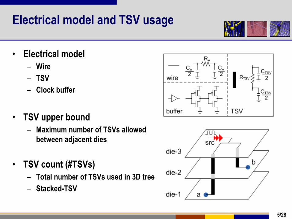
Electrical model and TSV usage
5/28
• Electrical model– Wire– TSV– Clock buffer
• TSV upper bound– Maximum number of TSVs allowed
between adjacent dies
• TSV count (#TSVs)– Total number of TSVs used in 3D tree– Stacked-TSV
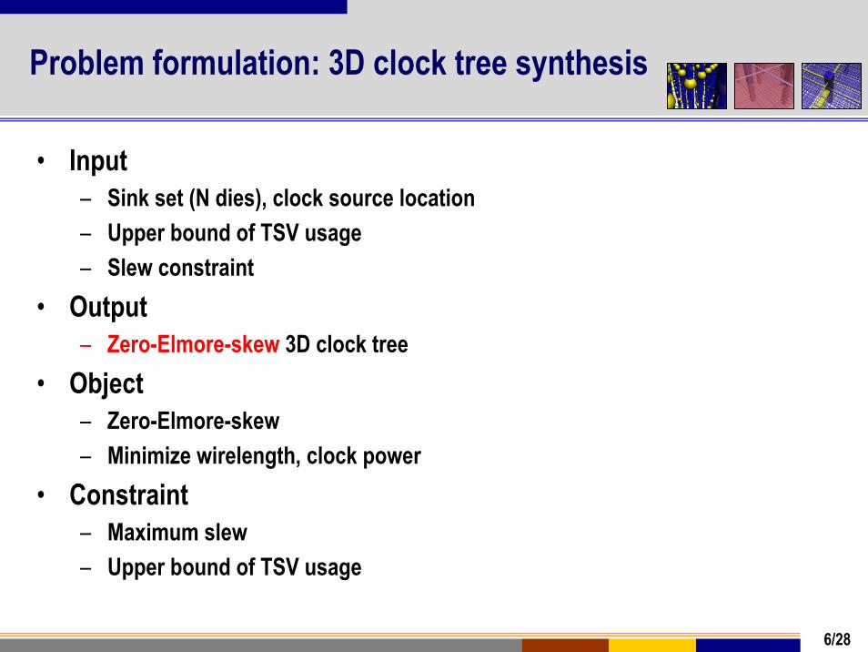
Problem formulation: 3D clock tree synthesis
• Input– Sink set (N dies), clock source location– Upper bound of TSV usage– Slew constraint
• Output– Zero-Elmore-skew 3D clock tree
• Object – Zero-Elmore-skew– Minimize wirelength, clock power
• Constraint – Maximum slew– Upper bound of TSV usage
6/28

3D clock tree design flow
• Input: – a set a sinks on N die– Upper bound of TSV
Upper bound of TSV = 3, clock source locates on die-07/28
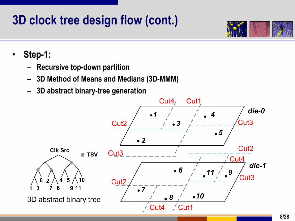
3D clock tree design flow (cont.)
• Step-1: – Recursive top-down partition– 3D Method of Means and Medians (3D-MMM)– 3D abstract binary-tree generation
8/28

3D clock tree design flow (cont.)
• Step-2: – Merging and slew-aware buffering, embedding– 3D clock tree with multiple TSVs
• Unique property of 3D clock tree– A complete tree + many sub-trees
9/28
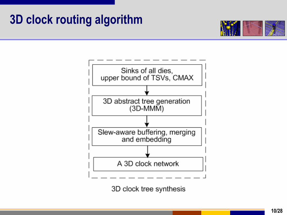
3D clock routing algorithm
10/28

3D-MMM and 3D abstract tree
11/28

3D-MMM and 3D abstract tree (cont.)
• 3D abstract tree for the N-die stack– N-colored binary tree– Clock source location
12/28

3D clock tree in multiple-die stack
13/28
• A complete tree + many sub-trees
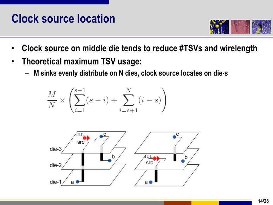
Clock source location
• Clock source on middle die tends to reduce #TSVs and wirelength• Theoretical maximum TSV usage:
– M sinks evenly distribute on N dies, clock source locates on die-s
14/28

Buffering and merging
• Goal– Slew control
Maximum loading capacitance (CMAX) of clock buffers– Wirelength reduction
• Object– Zero-Elmore skew– Clock power minimization
15/28

Detail experiment settings
• 45nm technology:– Frequency = 1GHz, Vdd = 1.2V– Clock slew < 10% of clock period (CMAX = 300fF)– Clock skew < 3%~4% of clock period– Wire: R = 0.1 Ω/um, C = 0.2 fF/um– Buffer: Rd=122 Ω, CL = 24 fF, td = 17 ps– TSV: RTSV = 0.035 Ω, CTSV = 15.48fF
• 10 um X 10 um, via-last• Thinned-die height = 20 um
• Results are from SPICE simulation– Skew, slew, power
• We use two cases: four-die and six-die
Circuits # Sinksr1 267r2 598r3 862r4 1903r5 3101
16/28

Sample 3D clock trees
17/28
r5, six-die
#TSVs = 20

Impact of TSV bound on wirelength and power
18/28
r5, six-die
Point A: 20% power saving, TSV bound ≥ 70% of #sinks
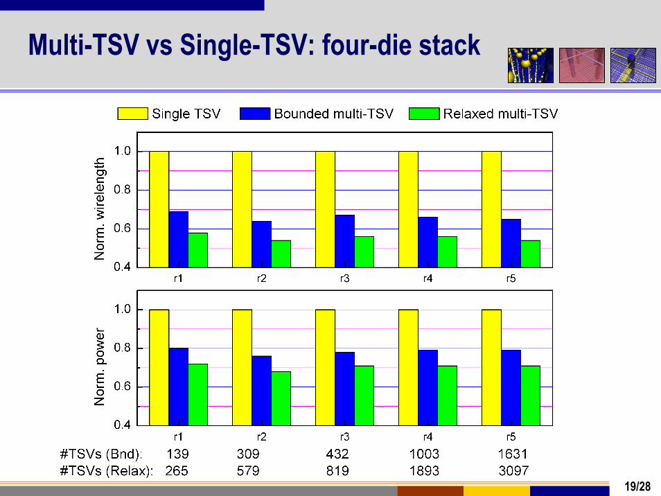
Multi-TSV vs Single-TSV: four-die stack
19/28

Multi-TSV vs Single-TSV: six-die stack
20/28

Clock skew in four- and six- die stack
21/28
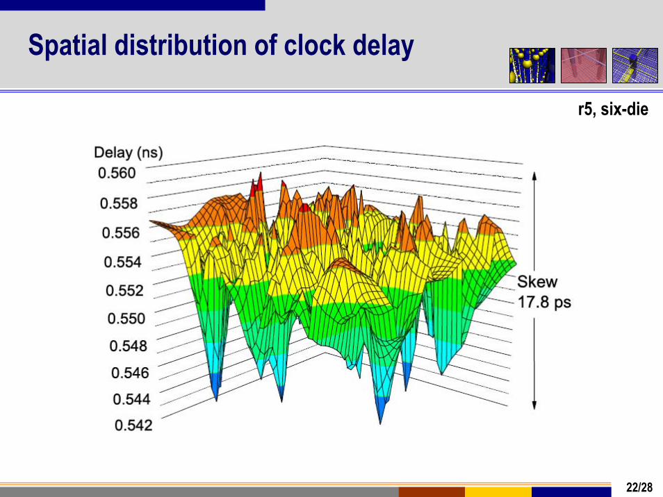
Spatial distribution of clock delay
22/28
r5, six-die

Impact of TSV bound on slew distribution
23/28
r5, six-dieCMAX=300fF
[11.4ps, 86.2ps]Avg. 53.9ps#Bufs: 2933
[10.9ps, 79.6ps]Avg. 42.6ps#Bufs: 2638

Impact of CMAX on slew variations
24/28
Using single TSV
Using multiple TSVs
r5, six-die
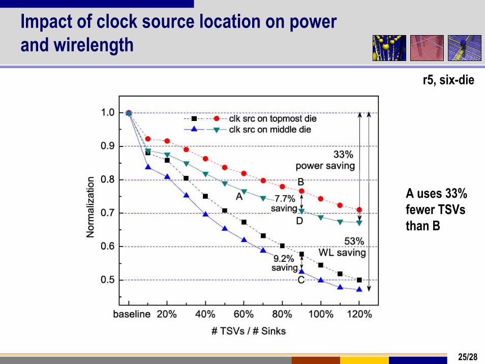
Impact of clock source location on power and wirelength
25/28
r5, six-die
A uses 33% fewer TSVs than B

Distribution of stacked-TSV heights
26/28
r5, six-die
#TSVs = 3720 #TSVs = 2791
Conclusions
• Explored design optimization techniques for reliable, low-power, low-slew 3D clock network design.
• Using multiple TSVs helps to reduce wirelength and power. Multi-TSV also has better control on slew variations.
• Smaller CMAX efficiently lowers the clock slew.
• Clock source location affects wirelength, power and TSV usage ofthe 3D clock network. Middle-die sourcing policy reduces the TSV usage under the same power budget.
27/28
Thank you
28/28