postal correspondence computer organizations · compliers generally works on polish notation. in...
TRANSCRIPT

GATE- 2016-17 Postal Correspondence 1
GATE & PSUs Postal Correspondence © 2015 ENGINEERS INSTITUTE OF INDIA® . All Rights Reserved28-B/7, Jia Sarai, Near IIT, Hauz Khas, New Delhi-110016. Ph. 011-26514888. www.engineersinstitute.com
ComputerOrganizations
Computer Science
&
Information Technology (CS)
20 Rank under AIR 100
Postal Correspondence Examination Oriented Theory, Practice Set
Key concepts, Analysis & Summary
GATE- 2016-17 Postal Correspondence 2
GATE & PSUs Postal Correspondence © 2015 ENGINEERS INSTITUTE OF INDIA® . All Rights Reserved28-B/7, Jia Sarai, Near IIT, Hauz Khas, New Delhi-110016. Ph. 011-26514888. www.engineersinstitute.com
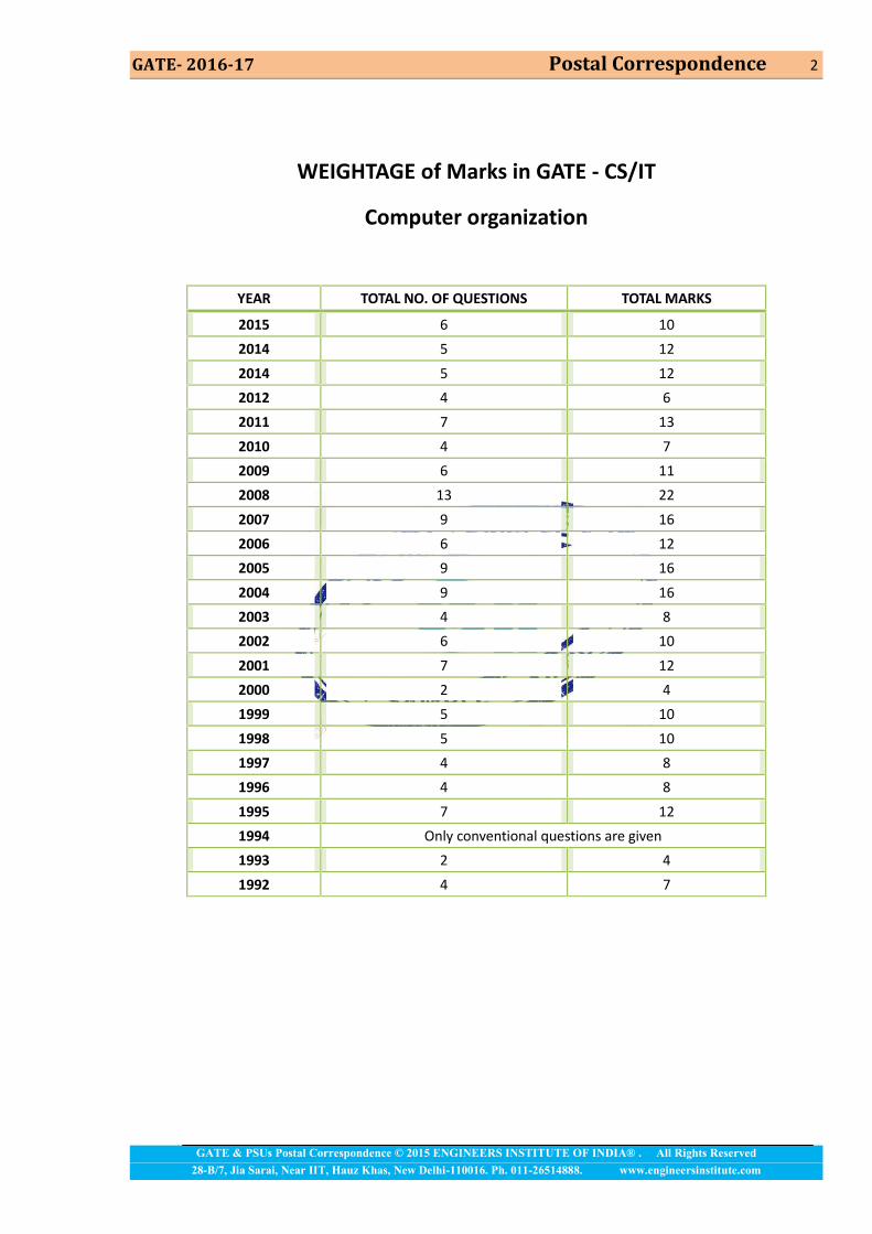
WEIGHTAGE of Marks in GATE - CS/IT
Computer organization
YEAR TOTAL NO. OF QUESTIONS TOTAL MARKS
2015 6 102014 5 122014 5 122012 4 62011 7 132010 4 72009 6 112008 13 222007 9 162006 6 122005 9 162004 9 162003 4 82002 6 102001 7 122000 2 41999 5 101998 5 101997 4 81996 4 81995 7 121994 Only conventional questions are given1993 2 41992 4 7
GATE- 2016-17 Postal Correspondence 3
GATE & PSUs Postal Correspondence © 2015 ENGINEERS INSTITUTE OF INDIA® . All Rights Reserved28-B/7, Jia Sarai, Near IIT, Hauz Khas, New Delhi-110016. Ph. 011-26514888. www.engineersinstitute.com
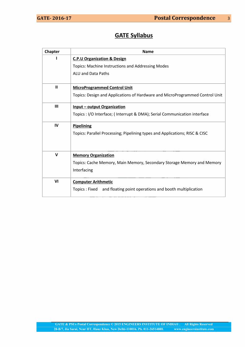
GATE Syllabus
Chapter NameI C.P.U Organization & Design
Topics: Machine Instructions and Addressing ModesALU and Data Paths
II MicroProgrammed Control UnitTopics: Design and Applications of Hardware and MicroProgrammed Control Unit
III Input – output OrganizationTopics : I/O Interface; ( Interrupt & DMA); Serial Communication interface
IV PipeliningTopics: Parallel Processing; Pipelining types and Applications; RISC & CISC
V Memory OrganizationTopics: Cache Memory, Main Memory, Secondary Storage Memory and MemoryInterfacing
VI Computer ArithmeticTopics : Fixed and floating point operations and booth multiplication

GATE- 2016-17 Postal Correspondence 4
GATE & PSUs Postal Correspondence © 2015 ENGINEERS INSTITUTE OF INDIA® . All Rights Reserved28-B/7, Jia Sarai, Near IIT, Hauz Khas, New Delhi-110016. Ph. 011-26514888. www.engineersinstitute.com
C O N T E N T
1. CPU ORGANIZATION & DESIGN ………………………………. 05-23
2. MICROPROGRAMMED CONTROL UNIT………………………. 24-27
3. INPUT – OUTPUT ORGANIZATION...…………………………… 28-43
4. PIPELINING...……………………………………………………….. 44-53
5. MEMORY ORGANISATION ....….……………………………….. 54-72
6. GATE Practice Set....….………… ….…………………………….... 54-72

GATE- 2016-17 Postal Correspondence 5
GATE & PSUs Postal Correspondence © 2015 ENGINEERS INSTITUTE OF INDIA® . All Rights Reserved28-B/7, Jia Sarai, Near IIT, Hauz Khas, New Delhi-110016. Ph. 011-26514888. www.engineersinstitute.com
CHAPTER-1
CPU ORGANIZATION & DESIGN
CPU (Central Processing Unit) is made up of three major parts:1. Arithmetic and Logic Unit (ALU)2. Control Unit (CU) and3. Processing Registers
ALU is used to perform the required Arithmetical and logical operation under the directions ofcontrol unit.
Control Unit supervises the transfer of information among the Registers and instructs the ALU thatwhich operation has to be perform.
Processing Registers are used to store the data during execution The Computer instruction set provides the specifications for the design of the CPU.Control Word: It is a binary word that is generated by the CPU to perform one of the various operations.Control Register: It is used to store the control word.
If the length of the control word is n bit, total no. of operations that can be used to perform 2n ;
ranges from 00----0 (n) to 1-----1(n) and each combination is used to assign one operation.Microoperation : It is an operation executed on data stored in registers. Micro operation is a basicregister to register operation. Instruction is divided into 2 parts:
1. Operation part (most side)2. Operand part (least side).
For ‘n’ address bit CPU total no. of memory location to be accessed is 2n and each memory location
is able to store 1 word. Length of the word varies from one CPU to other and depends on the no. of data bits that can be
transferred at a time (i.e. word size is equal to the no. of data bits a CPU has) The total memory is divided in to 2 parts namely
1. User memory 2.Stack memory User memory is under the control of only user, but stack memory is under the control of both CPU
and user.Different ways for performing the Arithmetical operations:
1. Infix notation (Ex : A+B)2.Prefix or polish (Ex : +AB)3.Reverse polish notation (Postfix) (Ex: AB+)
Stack works on postfix.

GATE- 2016-17 Postal Correspondence 6
GATE & PSUs Postal Correspondence © 2015 ENGINEERS INSTITUTE OF INDIA® . All Rights Reserved28-B/7, Jia Sarai, Near IIT, Hauz Khas, New Delhi-110016. Ph. 011-26514888. www.engineersinstitute.com
Conversion of Infix to RPNEx: 1 A B C D
= ( )AB CD = AB CD +
Ex: 2 ( ) [ ( ) ]A B C D E F
First complete the inner side of parenthesis
= ( )[ ( ) ]AB C DE F =
= ( )[ ]AB DE C F = AB DE C F
( ) ( )
( )
AB CDE F
AB CDE F
AB CDE F
Conversion of RPN to InfixEx:1 AB CD
= ( ) ( )AB CD
= ( ) ( )A B C D
= AB CDEx: 2 AB DE C F
= ( ) [ ( ) ]A B C D E F
RPN is used in some electronic calculators Before evaluating the operation, the arithmetic expression must be converted into RPN, the
operations are pushed on to stack in the order in which they appear.
Numerical example : for the data (3 4) (5 6) using RPN
34 56 Stack operations :
Compliers generally works on polish notation. In scientific calculators, some operations are performed with RPN and others with
polish notation. The bits of the instructions are divided into 2 fields, called as Operation field and Operand field.
GATE- 2016-17 Postal Correspondence 7
GATE & PSUs Postal Correspondence © 2015 ENGINEERS INSTITUTE OF INDIA® . All Rights Reserved28-B/7, Jia Sarai, Near IIT, Hauz Khas, New Delhi-110016. Ph. 011-26514888. www.engineersinstitute.com
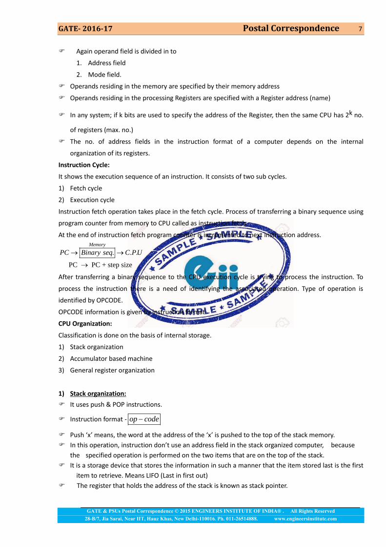
Again operand field is divided in to1. Address field2. Mode field.
Operands residing in the memory are specified by their memory address Operands residing in the processing Registers are specified with a Register address (name)
In any system; if k bits are used to specify the address of the Register, then the same CPU has 2k no.
of registers (max. no.) The no. of address fields in the instruction format of a computer depends on the internal
organization of its registers.Instruction Cycle:It shows the execution sequence of an instruction. It consists of two sub cycles.1) Fetch cycle2) Execution cycleInstruction fetch operation takes place in the fetch cycle. Process of transferring a binary sequence usingprogram counter from memory to CPU called as instruction fetch.At the end of instruction fetch program counter is incremented to next instruction address.
. . .
PC PC + step size
Memory
PC Binary seq C PU
After transferring a binary sequence to the CPU execution cycle is trying to process the instruction. Toprocess the instruction there is a need of identifying the associated operation. Type of operation isidentified by OPCODE.OPCODE information is given by instruction format.CPU Organization:Classification is done on the basis of internal storage.1) Stack organization2) Accumulator based machine3) General register organization
1) Stack organization: It uses push & POP instructions.
Instruction format - op code
Push ‘x’ means, the word at the address of the ‘x’ is pushed to the top of the stack memory. In this operation, instruction don’t use an address field in the stack organized computer, because
the specified operation is performed on the two items that are on the top of the stack. It is a storage device that stores the information in such a manner that the item stored last is the first
item to retrieve. Means LIFO (Last in first out) The register that holds the address of the stack is known as stack pointer.
GATE- 2016-17 Postal Correspondence 8
GATE & PSUs Postal Correspondence © 2015 ENGINEERS INSTITUTE OF INDIA® . All Rights Reserved28-B/7, Jia Sarai, Near IIT, Hauz Khas, New Delhi-110016. Ph. 011-26514888. www.engineersinstitute.com
Push and pop are used to access stack memory.
For accessing 2n words stack memory, the length of the (stack pointer) required is ‘n’ bits.
Always, SP is pointed at top of the stack; it is decremented during push operation and incrementedduring pop operation.
In 8085 for pushing pre decrement and for poping post increment 2 no. of flags are used to know the status of the stack: 1. Empty 2. Full Initially, stack cleared to ‘0’. So EMPTY is set and Full is cleared. If all memory locations are filled in the stack; then empty flag resets and Full flag sets. But most computer do not provide hardware for checking over flow (Full stack) or under flow
(empty stack); In this case the stack limits can be checked by using 2 processing Registers. One to hold the upper limit and other to hold the lower limit address After PUSH operation; SP is compared with the upper limit Register (SP is stack pointer) After POP operation SP is compared with the lower limit register2) Accumulator based machine: (Advantage: length of the opcode is low, so it can be executed at
faster rate.) In this all operations are performed with an implied accumulators It has only one address field. Instruction format:
op code Address
Ex: ADD xSUB x where ‘x’ is the address of the operand
3) General Register organization: (Length of the OP code is more)The instruction format needs 3 Register address fields or 2 Register address fields.Ex: ADD R1, R2, R3
R1=R2+R3 For data transfer MOV operations, it requires 2 no. Registers.Ex: MOV R1, R2
For Arithmetical; 3 Register RequiredFor Data transfer; 2 Register Required
Depending on the length of the operand, instructions are divided as follows:Instruction based on number of addresses
There are 5 type of instruction based on address:
(i) 4 – address instruction
(ii) 3 – address instruction
(iii) 2 – address instruction
(iv) 1 – address instruction
(v) 0 – address instruction.
(i) 4 – address instruction

GATE- 2016-17 Postal Correspondence 9
GATE & PSUs Postal Correspondence © 2015 ENGINEERS INSTITUTE OF INDIA® . All Rights Reserved28-B/7, Jia Sarai, Near IIT, Hauz Khas, New Delhi-110016. Ph. 011-26514888. www.engineersinstitute.com
In the 4 – address instruction, we have to specify 4-address, in which first address that is close to OP
code determines the result and the last address determines the address of the next instruction.
For example: ADD A1 A2 A3 A4
In this we performed the addition of M[A2] and M[A3] and the result is stored in M[A1]. Here A4
contains the address of next instruction.
(ii) 3 – address instruction
In the 3 – address instruction, we have to specify 3 – address in which the first address that is close
to OP code determines the result of operation.
Example:
ADD A1, A2 A3
First we performed the M[A2] + M[A3]
Next move the reject to A1.
M[A1]M[A2] + M [A3]
(iii) 2-address Instruction
In the case of two – address instruction, the accumulator is used to store the result.
Example:
ADD X, Y
It represents
AC: X + Y
In the 2 – address instruction another position is there without using accumulator for example:
ADD X, Y
It can be performed as:
X: = X + Y
The addition operation stored the result into X.
(iv) 1-address instruction
In the one – address instruction we use accumulator. The unspecified operands are assumed to
be stored in AC (Accumulator)
For example:
ADD X
It performed as
AC: = AC + X
(v) 0 – address instruction
A few computers name teen designed so that most instruction contain no explicit address; they
can be called as zero – address machine
All operands used by a zero address instruction are required to be in the top location in the stack.
Example: ADD
That causes the top two operands which should be X and Y, to be removed from the stack and
addressed the resulting sum X + Y is then placed at the top of the stack.
Addressing Modes
GATE- 2016-17 Postal Correspondence 10
GATE & PSUs Postal Correspondence © 2015 ENGINEERS INSTITUTE OF INDIA® . All Rights Reserved28-B/7, Jia Sarai, Near IIT, Hauz Khas, New Delhi-110016. Ph. 011-26514888. www.engineersinstitute.com
It is the way of locating the data in the operand field. The control unit of a computer is designed to go through the instruction cycle that is divided into 3
major phases (steps)1.Fetch the instruction from memory2.Decode the instruction and Execution
Program counter is used to store the address of the next instruction to be executed, and it isincremented each time to step size to point the next instruction.
The step-size is depending on the length of instruction. Decoding done in step 2 determines the operation to be performed and addressing mode of the
instruction. Then computer executes the instruction and returns to the step 1 to fetch the next instruction.
So, to know about the functions of decoding unit, it is compulsory to know about the addressingmodes.
Different Addressing Modes (AM)Implied AM: It has no operand fieldEg: CMA, HLT, NOP, andAll zero address instructionIt is also known as implicit (AM)Immediate AM: In this operand part is nothing but data. This AM is used to access the constants.These are useful for initializing Register for constant valuesEx: MOVI AX, 1234H, Add 0 #23 [# and I Denotes Immediate AM].Register AM: In this operand field must be specified with RegisterEx: 1.MOV AX, BX 2. ADD, CX, DXRegister indirect: In this, the specified register in the CPU whose content gives the address of theoperand in the memory.Ex: MOV AX, [BX]
ADD AX, [BX]In this example BX register is used to store the address of the operand i.e. content of the BX register actsas Effective Address (EA)Effective address is an address where data is availableDirect Addressing mode: In this EA=Address of the instruction (In branch type instruction, the addressfield specifies the actual branch address)Ex: MOV AX,[5555H]
JMP 2500HIndirect Addressing mode: In this, address field of the instruction gives the address where the effectiveaddress is stored in the memory.Relative Addressing mode: In this, the content of the pc is added to the address part of the instruction inorder to obtain the effective addressEx: ADD AX,[+25,BX] EA=BX+25

GATE- 2016-17 Postal Correspondence 11
GATE & PSUs Postal Correspondence © 2015 ENGINEERS INSTITUTE OF INDIA® . All Rights Reserved28-B/7, Jia Sarai, Near IIT, Hauz Khas, New Delhi-110016. Ph. 011-26514888. www.engineersinstitute.com
Indexed Addressing mode: In this mode the content of the Index register is added to the address part ofthe instruction to obtain the EA. Index Register is a special CPU register.Auto increment or Auto decrement Addressing mode: This is similar to the indirect mode except thatthe register is incremented or decremented after its value is used to access memory. This mode is used toAccess the Linear Array Elements.Base Register Addressing Mode: In this mode the content of a base register is added to that address partof the instruction to obtain the effective address.This is similar to the index AM except that the register is now called a base register instead of an Indexregister.NOTE: It is same as the register indirect mode except that is incremented to 401 after the instructionexecution but in Auto decrement mode it is decremented prior to the execution.
Classification of Instruction Sets: Instruction set indicate the no of possible operation in the processor.The processor supports 3-category of operation:1. Data transfer2. Data Manipulation3. Transfer of control (program controlData transfer Instructions:These are used to transfer the data from one place to other place without changing the data content.
LD Load
ST StoreMOV Move
XCH Exchange
IN Input

GATE- 2016-17 Postal Correspondence 12
GATE & PSUs Postal Correspondence © 2015 ENGINEERS INSTITUTE OF INDIA® . All Rights Reserved28-B/7, Jia Sarai, Near IIT, Hauz Khas, New Delhi-110016. Ph. 011-26514888. www.engineersinstitute.com
OUT Output
PUSH PushPOP Pop
Data manipulation Instructions: While execution of this instruction one from of data is converted intoanother form.These are used to perform various operations on dataAgain these are divided as follows :a. Arithmetical b. Logical c. ShiftArithmetical
INC IncrementingDEC Decrementing
ADD Addition
SUB SubtractionSUBB Subtract with borrow
MUL Multiplication
DIV DivisionADDC Add with carry
NEG 2’s Complement
Logical & Bit Manipulation instructions:CLR ClearCMA Com or complement Accumulator
CLRC Clear carry
SETC Set CarryCOMC Complement carry
EI Enable Interrupt
DI Disable interruptXOR Exclusive OR
Shift Instruction: There are used to double or half the give dataShift left = doubles the data (Multiply by 2)Shift right = Half the data (Divide by 2) with error for odd digitsThere are 3 types of shift1) Logical2) Arithmetical

GATE- 2016-17 Postal Correspondence 13
GATE & PSUs Postal Correspondence © 2015 ENGINEERS INSTITUTE OF INDIA® . All Rights Reserved28-B/7, Jia Sarai, Near IIT, Hauz Khas, New Delhi-110016. Ph. 011-26514888. www.engineersinstitute.com
3) Rotate typeLogical Arithmetical Rotate type (circular)SHR SHRA ROR-Rotate right without carry
SHL ASHL ROL-Rotate left without carryLSB or MSBIs lost if carry flag is not used
SHLA RCR-Rotate right with carry
RCL-Rotate left with carry
Parity bit is not modified during the execution of ROR and ROL, but for other; parity flag may bemodified.Program control instructions These are used to transfer the program execution from current memory location to the required
memory location. Each time after executing one instruction, PC is automatically incremented to step size. Branch and jump may be conditional or unconditional All jump and branch instructions are used to transfer the program execution permanently but call
instruction transfer the program execution temporarilyDifferent types of jumps :
Branch BR
Jump JMPSkip SKP
Call CALL
Return RETCompare CMP
Test TST
Skip instruction does not need an address field Call and RET are used in subroutines CMP and TEST instructions are used to check the status of the flag and Register content is not altered Flags are also known as conditional code bits
Flag
Flag is a flip-flop. Flip-flop is a bi-state device that is set or reset. Flags are divided into two types:
GATE- 2016-17 Postal Correspondence 14
GATE & PSUs Postal Correspondence © 2015 ENGINEERS INSTITUTE OF INDIA® . All Rights Reserved28-B/7, Jia Sarai, Near IIT, Hauz Khas, New Delhi-110016. Ph. 011-26514888. www.engineersinstitute.com
(i) Conditional Flag (ii) Control Flag
Conditional Flag:
These flags are set or reset based on the result nature of ALU. They are divided into six types:
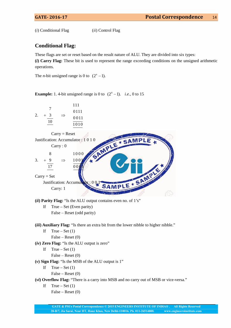
(i) Carry Flag: These bit is used to represent the range exceeding conditions on the unsigned arithmetic
operations.
The n-bit unsigned range is 0 to (2 1).n
Example: 1. 4-bit unsigned range is 0 to 4(2 1). i.e., 0 to 15
2.
1117
01113
0 01110
1010
Carry = Reset
Justification: Accumulator : 1 0 1 0
Carry : 0
3.
8 10 0 0
9 10 01
17 0 0 01
Carry = Set
Justification: Accumulator : 0 0 1
Carry: 1
(ii) Parity Flag: “Is the ALU output contains even no. of 1’s”If True – Set (Even parity)
False – Reset (odd parity)
(iii) Auxiliary Flag: “Is there an extra bit from the lower nibble to higher nibble.”If True – Set (1)
False – Reset (0)
(iv) Zero Flag: “Is the ALU output is zero”If True – Set (1)
False – Reset (0)
(v) Sign Flag: “Is the MSB of the ALU output is 1”If True – Set (1)
False – Reset (0)
(vi) Overflow Flag: “There is a carry into MSB and no carry out of MSB or vice-versa.”If True – Set (1)
False – Reset (0)

GATE- 2016-17 Postal Correspondence 15
GATE & PSUs Postal Correspondence © 2015 ENGINEERS INSTITUTE OF INDIA® . All Rights Reserved28-B/7, Jia Sarai, Near IIT, Hauz Khas, New Delhi-110016. Ph. 011-26514888. www.engineersinstitute.com
New Edition with GATE 2015 Solutions is available.
GATE Classroom Coaching
GATE Postal Correspondence Coaching
GATE Online test Series
To Buy Postal Correspondence Package call at 0-9990657855