polycrystal orientation maps from tem -...
TRANSCRIPT
This is an electronic version of an article whose final and definitive form has been published in Ultramicroscopy
(Volume 96, Issue 2, August 2003, Pages 127-137) (Elsevier); Ultramicroscopy is available online at:
http://www.sciencedirect.com/.
Polycrystal orientation maps from TEM
by J.-J.Fundenberger1, A.Morawiec
2, E.Bouzy
1 and J.S.Lecomte
1
1 Laboratoire d'Etude des Textures et Application aux Materiaux (LETAM)
Institut Superieur de Genie Mecanique et Productique
Universite de Metz, Metz, France
2 Instytut Metalurgii i InŜynierii Materiałowej PAN, Kraków, Poland.
Abstract
Determination of topography of crystallite orientations is an important technique of investigation of
polycrystalline materials. A system for creating orientation maps using TEM Kikuchi patterns and
CBED patterns is presented. The orientation maps are obtained using a step-by-step beam scan on a
computer controlled TEM equipped with a CCD camera. At each step, acquired diffraction patterns
are indexed and orientations are determined. Although, the approach used is similar to that applied
in SEM/EBSD orientation imaging setups, the TEM based system considerably differs from its
SEM counterpart. The main differences appear due to specific features of TEM and SEM
diffraction patterns. Also the resulting maps are not equivalent. On these generated by TEM, the
accuracy of orientation determination can be better than 0.1 degree. The spatial resolution is
estimated to be about 10nm. The latter feature makes the TEM orientation mapping system an
important tool for studies at fine scale unreachable by SEM/EBSD systems. The automatic
orientation mapping is expected to be a useful complement of the conventional TEM contrast
images. The new technique will be essential for characterization of fine structure materials. To
illustrate that, example maps of an Aluminum sample produced by severe plastic deformation are
included.

PACS : 07.78; 61.14; 61.14.Lj; 81.40; 81.40.Ef
Keywords: Instrument control and alignment; Electron diffraction; Convergent beam Electron
Diffraction (CBED); Data processing/ image processing.

Introduction
There are several methods to determine crystal orientations from TEM electron diffraction patterns.
The oldest and frequently used technique is to analyze the spot diffraction patterns. Numerous
authors use Selected Area Diffraction (SAD) in polycrystals to get a rough idea of the
misorientation of crystals in the illuminated area. Several years ago, Schwarzer [1, 2] has proposed
a method to get pole figures in the TEM by recording the diffracted intensity in SAD as a function
of the specimen orientation. The correlation between the orientation and the precise spatial location
is lost in this technique. Orientation based microstructure maps can be obtained using the ‘Dark
Field Scanning’ commercially distributed by EDAX/TSL. In this case, the orientation of a point
(pixel) in the image is determined from intensities obtained for various incident beam directions.
For all the methods based on spot diffraction patterns the orientation accuracy is low - about 5 deg.
Even if the indexing procedure takes into account the intensity of diffraction spots, the accuracy is
not better than 1 degree [3, 4].
Kikuchi patterns have been used for orientation determination for a long time [5]. Also orientation
maps based on Kikuchi patterns in TEM have already been published [6, 7]. These maps, however,
were created by tedious manual data collection. Grains were identified based on contrast images of
the microstructure. With manually controlled microscopes, diffraction patterns were acquired for a
number of grains and grain orientations were determined. The whole procedure was time
consuming and prone to errors and bias due to the subjective choice of grains. Moreover, with this
technique, small orientations changes within grains are not detected.
Fully automatic creation of orientation maps by electron back scattered diffraction (EBSD) or
channeling patterns on SEM is already a well established technique. Analogous method based on

Kikuchi patterns or convergent beam electron diffraction (CBED) patterns can be applied for
getting orientation maps on transmission microscopes. TEM offers the advantage of better spatial
resolution and better accuracy in relative orientations. In applications, these two aspects are
essential for ultra-fine microstructure and sub-grain characterization. However, difficulties with
automatic line detection and slightly more complicated indexing (due to the smaller acquisition
angle and higher indices of the diffracting planes) hindered the development in creation of
orientation maps on TEM.
This paper introduces the first system of that kind recently implemented at LETAM. After a short
description of the experimental setup, the pattern acquisition and correction procedures are
presented. Then, main features of the line detection and indexing routines are described. Moreover,
the spatial resolution, the orientation accuracy and the future developments are discussed. As an
example, maps of an Aluminum sample illustrating capabilities of the system are given.
Elements of the system
The diffraction diagrams are obtained with a Philips CM200 transmission electron microscope
operating at 200kV. A LaB6 cathode is used as electron source. This type of TEM can be nearly
fully controlled using the Philips software version 11.2. The microscope is equipped with a
computer controlled goniometer stage (CompuStage). The acquisition of the diagrams is made
thanks to a 1K × 1K GATAN 791 slow scan CCD camera. On top of the CCD detector, a YAG
scintillator is used as the primary screen. The camera is mounted on the 35mm port above the
viewing chamber. In this position, the solid angle which is seen by the CCD detector is as large as
possible. As the maximum diffraction angle in this TEM is about ± 10°, the whole wide-angle view
of the pattern can be detected by the camera for the microscope camera length of about 82mm at
the CCD level (which corresponds to 320mm at the viewing screen level). A lower value just

reduces the size of the patterns without adding further information. A larger value reduces the
visible solid angle.
The camera has a 14-bit digitalisation depth, which leads to a high dynamic range. Both, the
camera and the TEM are controlled from a personal computer running GATAN Digital Micrograph
software (version 3.3.0). Schematic configuration of the system used to build the orientation maps
is shown in Fig.1.
Pattern acquisition and image correction
It is worth to recall briefly the TEM settings leading to the diffraction modes we are interested in.
(More information can be found in works of Morniroli [8], Tanaka [9] or Steeds [10] covering the
convergent beam electron diffraction methods in detail.) By varying the beam convergence angle
2α (using the second condenser aperture), different patterns are obtained. As α increases, the
diffraction pattern changes from a spot pattern when α << θB (where θB stands for the Bragg angle)
to a Kikuchi pattern when α < θB, and to a CBED pattern when α >θB. The geometry of CBED
patterns is the same as the geometry of Kikuchi patterns: for each (hkl) plane, pairs of lines being
parallel to the trace of the crystallographic plane are formed. However, the mechanisms of pattern
formation are different. Kikuchi lines appear in two steps. First, the beam becomes divergent by
inelastic scattering. Second, the electrons in exact Bragg conditions are elastically scattered on
crystallographic planes. To observe a Kikuchi diffraction pattern the sample has to be thick enough.
On the other hand, Kossel lines in CBED patterns appear in a single step. As α is large, there are
already electrons in the beam which are in Bragg conditions and are elastically scattered by the
plane even if the sample is thin. For a given Kossel pattern, a superimposing Kikuchi pattern is
always present.

The CCD camera applied in the system is capable of providing 1024 × 1024 pixel images. In
practice, consolidated images of reduced size (512 × 512 pixels) are used; the binning of 4 pixels
into 1 improves dynamics and speeds up the transfer and further treatment of the image. The loss of
accuracy in locating lines caused by the binning does not affect the result if the thickness of the
lines is in the order of several pixels of the original image, and that is the case in most practical
applications.
The common characteristic of the diffraction diagrams is that the central area is much brighter than
the border. It is possible to acquire two images with different exposition times. The first image is
acquired with a short exposition time in order to get the central area of the pattern. The second
image is taken with a longer exposition time; in this case the central area of the CCD is saturated,
but the lines at the border of the diffraction pattern are enhanced. Additionally, the recorded
diagrams must be corrected for varying intensity. The procedure proposed by Krieger Lassen [11]
has been applied. In this correction scheme, the logarithm of intensity at each pixel is calculated,
and then the background is modified by applying a heavy low-pass filter. The contrast of the
Kikuchi lines is enhanced in the border as well as in the central area of the diffraction patterns. The
correction procedure makes the lines more visible but also changes the contrast of the patterns. In
some cases, a dark edge is added to the bright lines. Example CBED patterns before and after
image correction are shown in Fig.2.
Line detection and indexing
Line detection is essentially an issue which belongs to image analysis. However, the diffraction
patterns used for mapping have some specific features which must be taken into account. TEM
diffraction patterns exhibit a large variety of such features, and this complicates the problem of line
detection. One would like to have a flexible routine working for Kikuchi and CBED patterns, and

for various operating conditions of the microscope. This means that the objects to be detected can
be sharp lines or diffuse bands and both can be bright or dark; additionally, a line can be dark in
one part and bright in another, or it can be dark on one side and bright on the other. As pointed out
in the previous section, the correction procedure induces some contrast changes on line edges (Fig.
2). The contrast of the diffraction pattern varies also with the specimen thickness. In thin areas, the
diffraction pattern shows deficit and excess Kikuchi lines. For larger thickness, Kikuchi bands are
visible [12]. A program capable of handling this variety of situations was created simply by trying
various versions and comparing their efficiency in terms of the number of correctly detected line
pairs and the execution time. Generally, we followed the developers of the EBSD-based systems
and used the Hough transform as the main tool with numerous additions to the standard procedure.
In order to improve temporal efficiency of the program, constant factors involved in the transform
are calculated beforehand. The are a number of strategies suitable for various image types. In the
main one, addtional binning of patterns from 512x512 to 256x256 pixels is used. To enhance the
maxima of the Hough transform, a small (5x5) Gaussian shaped mask is applied. By locating
maxima of the transform, individual lines are detected. The program is greedy and tries to identify
as many lines as possible. Then, lines with similar inclinations (i.e., nearly parallel) are grouped
together to create pairs. A pair is accepted as genuine only if the distance between lines of a pair is
within brackets determined by the list of reflections. The efficiency and reliability of our algorithms
still depend on the quality of the diffraction pattern but they are sufficient for most applications. It
is believed, however, that they can be considerably improved.
Ascribing indices to detected reflections (indexing) is the next step towards orientation
determination. It is convenient (and in most practical cases sufficient) to use indexing based on the
geometry of diffraction patterns without taking into account intensities of particular reflections.
Kikuchi and CBED patterns have the same diffraction geometry as EBSD and channeling patterns.
Essentially the same principles are applicable for indexing in all these cases. The main difference is
that the solid angle acquired on a given TEM pattern can be considerably smaller than in the case of
SEM patterns. That angle is directly related to the effective camera length. In the TEM, the latter is
usually an order of magnitude larger than on SEM. Also the number of lines is larger in the case of
TEM.
Because of the small acquisition angle, high index reflections must be taken into account. This
makes the indexing slightly less reliable but in cases of high crystal symmetry the effect is usually
negligible. On the other hand, the larger sample to detector distance gives a better accuracy in
orientation determination. (This, unfortunately, applies only to two out of three parameters of
orientation; the subject is discussed below.)
The temptation to increase accuracy by increasing the camera length is tempered by the decreasing
acquisition angle; there is a limit beyond which the patterns cannot be efficiently indexed. With our
experimental setup, for cubic materials this limit corresponds to the camera length of about 300mm
at the CCD level (and 1200 mm at the viewing screen).
A detailed description of the applied indexing software can be found in [13]. Our experience shows
that this software is robust and very efficient for indexing TEM line diffraction patterns. The TEM
based line diffraction patterns allow one to get both the position and the width of the bands with
relatively high accuracy; therefore the indexing ambiguities are in most of the cases avoided. A
CBED pattern with indexing based on automatically detected lines is shown in Fig.2c.
Mapping
An orientation map is created by scanning an area of the specimen step by step. At each point a
diffraction pattern is acquired, corrected and stored. The line detection, pattern indexing and
orientation determination are made off-line on another computer. Scanning an area of the specimen
can be achieved by moving the specimen using a mechanical stage. This method, however has low
positional accuracy, especially when the step size is small. Furthermore, after each movement, the
mechanical stage needs a stabilization time. An alternative method, which is applied in our system,
is to scan the area by moving the beam. The beam is directed by the current in the beam deflection
coils, which is controlled by the computer. The beam movement has to be calibrated once for each
magnification in a given mode and at a given accelerating voltage. In order to avoid long range
drift, thermal stability of the microscope and the sample holder has to be reached. Absence of a
global drift is confirmed by the return of the beam to the starting point after completion of the
mapping procedure. It can be also verified by taking a look at the grid of contamination marks.
Generally, the drift is negligible. However, some small local distortions of the measurement grid
are permitted if they do not influence the overall result.
Once the orientations in the grid on the investigated area are known, the task is to represent the
data. The character of the data originating from a TEM is the same as in the SEM/EBSD systems.
Therefore, the same post-processing can be applied. The most natural step is to create a map with
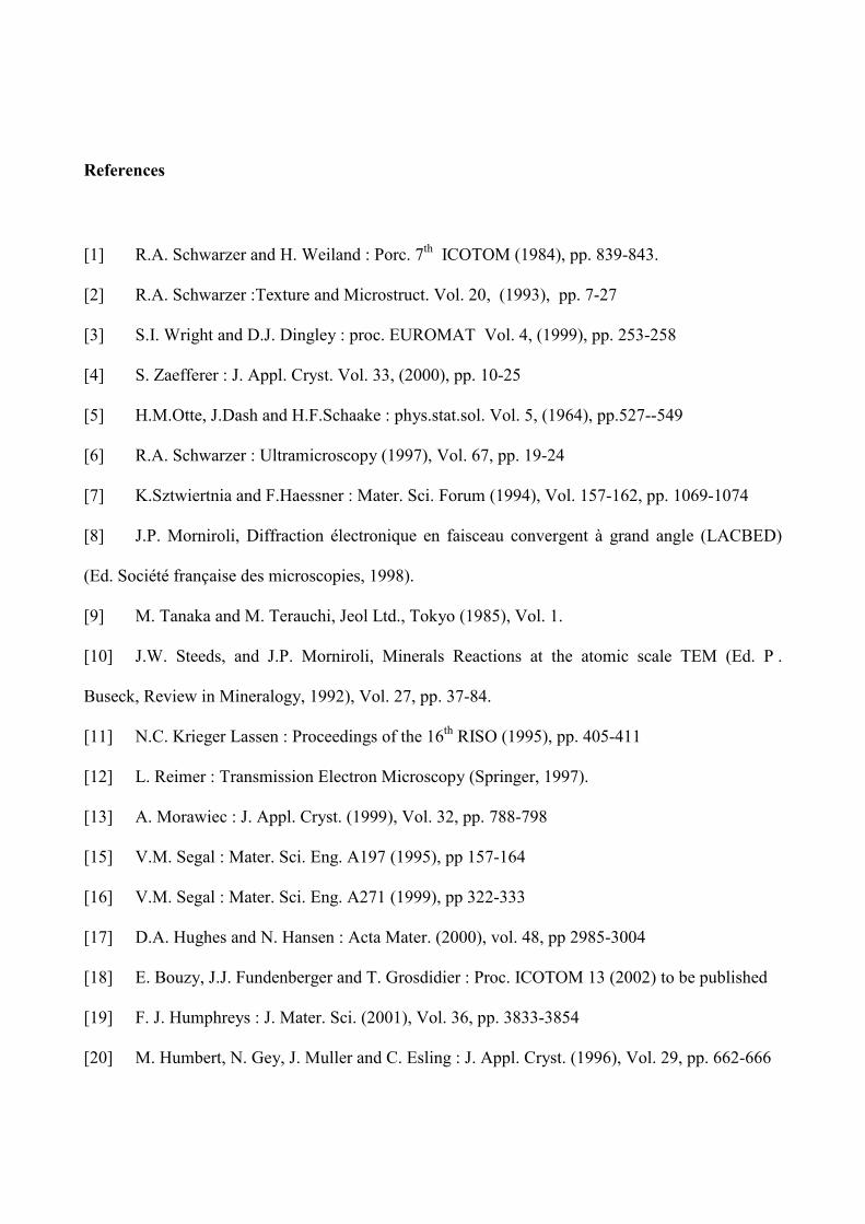
false colors ascribed to orientations. In example maps given below we use the code ascribing a
color based on the crystallographic direction parallel to the X (tilt). axis. Another simple option is
to add boundaries between neighboring points with misorientation angle exceeding a chosen limit.
By converting the TEM data, the post-processing software of the existing SEM/EBSD systems can
also be used.
Example
The new method has been applied to a number of metallic samples in areas of severe deformation
(e.g., shear bands). Detailed discussion of results will be published elsewhere. Here, to illustrate the
technique, some orientation maps from an Aluminum sample deformed by Equal Channel Angular
Extrusion (ECAE) [15, 16] will be presented. The aim of this deformation process is to produce
fine grained material in bulk form. The sample we studied has been extruded through a die 8 times

at room temperature. Between each pass, the sample was rotated by 180° around the extrusion
direction. This deformation path is called ‘route C’. The cumulative deformation reaches the value
of 4.5. The main goal of the study was to identify orientation heterogeneities. The microstructure
has a multi-scale character comparable to samples obtained after severe plastic deformation by
conventional processes like rolling [17]. Using optical microscopy, the primary large grains (few
hundred µm) can be recognized. Inside the initial grains bands are visible. The width of these bands
is in the order of 10µm. Our TEM observations show that inside the bands cells of the size of 1µm
are present.
The orientation map in TEM scale allows to identify the nature of the sub-grain boundaries of the
cells structures present in an ECAE sample and revealed clearly the orientation heterogeneities
resulting from local deformation inhomogeneities [18].
Two orientation maps of an aluminum sample deformed by ECAE are shown in Figs 3a and b. The
first one is based on the Kikuchi patterns, the other one is based on the CBED patterns. Both maps
were made on the same sample at almost the same location. For both maps, the camera length was
82mm at the CCD level. An area of 2x2µm was scanned in steps of 20nm. The color code gives the
crystallographic direction parallel to the X axis of the sample. No filtering was applied; the
presented results are as they came out from the orientation determining procedure.
For creation of the map based on Kikuchi patterns the spot size was about 10nm. Orientations could
not be determined from the Kikuchi patterns at 9.4% of points. Most of them were located at the
grain boundaries. When the electron beam hits a boundary, the acquired diffraction pattern
originates from two crystallites and is a superposition of two single crystal patterns; in such cases,
indexing is difficult. In some regions, the density of defects induces a degradation of the diffraction
pattern quality making the line detection difficult. In these cases, the indexing procedure fails
because the number of detected lines which are actually correct is not sufficient.
The CBED patterns were collected with the angle α set to 1.5°. Orientations were not determined
from these patterns at about 2% of points. For the same reasons as before, these points are not
randomly distributed, but are located at grain boundaries.
In the considered case, the CBED based map is more reliable despite the fact that the acquisition of
CBED patterns followed the collection of the Kikuchi patterns; the order matters because of the
contamination of investigated area. The spatial resolution of CBED based map is better because in
the nanoprobe mode the spot size can be smaller than in microprobe mode used to get Kikuchi
patterns. On the other hand, the CBED patterns are sensitive to the focus of the beam on the
specimen. For example, if the sample is not flat, the interaction volume changes from one point to
another and thus, the spatial resolution may deteriorate. Especially, when the sample is tilted, a
focusing correction procedure would have to be applied. In practice however, when making the
orientation mapping, there is no need to tilt the sample. Another point is that the CBED patterns are
sensitive to internal stresses caused by defects and the lines inside the transmitted spot become
distorted.
Discussion
Spatial resolution
The most interesting problems in investigation of polycrystalline materials require high spatial
resolution. The spatial resolution on SEM with conventional tungsten or LaB6 filament is limited to
hundreds of nanometers. The limit is considerably lowered to about 50nm by the use of a field
emission gun (FEG) [19].
TEM offers even better resolution. In the nanoprobe mode, the probe size can be reduced to a few
nanometers. The lower limit of the probe size is connected to the brightness of the thermo-ionic

sources. Below 2 nm the signal becomes weak. For very small probe sizes (less than 1 nm), it is
recommended to use a TEM equipped with FEG because the brightness of this electron source is
much higher in these conditions. One has to notice that a reduction of the probe size weakens the
diffraction signal due to the smaller diffracting volume and the probe current density; as a
consequence, the pattern quality deteriorates.
The most essential limit seems to be related to the sample thickness. The thickness together with
the convergence angle determine the diffracting volume. The latter is the ultimate measure of the
spatial resolution.
Generally, it is difficult to evaluate the spatial resolution because of a large number of factors
involved. With our configuration, for a reasonable acquisition time, the limit seems to be about
10nm.
Orientation accuracy
The determination of absolute orientations depends mainly on the sample preparation and the
precision of positioning the sample in a TEM sample holder. With standard procedures for sample
preparation it is difficult to get accuracy better than a couple of degrees.
However, in most TEM applications the main interest is not in absolute orientations but in relative
orientations. In this case a considerably better precision can be achieved. The accuracy of relative
orientations is linked to the effective camera length. Because it is considerably larger than the SEM
'sample to detector distance', the TEM technique is more precise. On TEM, the rotations with axes
perpendicular to the microscope axis can be determined with higher precision. On the other hand,
the accuracy of the angle of rotation about the microscope axis is limited by the thickness of the
detected lines and ultimately, in the case of very thin lines, by the size and resolution of the pattern
detector.
A simple way to estimate the accuracy of automatic orientation determination is by checking the
misorientation angle profile along a line on a single crystal. The profile represents the

misorientation angles between orientations measured at particular points and the average crystal
orientation [20]. A silicon single crystal was used to make 100 measurements along a 1µm long
line with a constant step size of 10nm. The line scan has been repeated for 2 diffraction camera
lengths (82mm and 159mm at the CCD level), in microprobe mode (Kikuchi patterns) and in
nanoprobe mode (CBED patterns). The misorientation angle profiles are shown Fig.4. Except for 5
points (out of 400) all the misorientations are smaller than 0.2°. For the larger camera length
(159mm), the misorientations are almost within 0.1°. With this large camera length, better
precision is obtained for CBED patterns; in this case the misorientation is around 0.05°.
Efficiency
Temporal efficiency of the map creation is limited by the pattern acquisition and the line detection
procedures. With the resolution of 512x512 pixels, the rate of pattern acquisition is about 5-7sec
per pattern. As for the line detection, there is always a trade off: the more reliable results are
required, the more time it takes to get them. A reasonably good procedure for line detection used in
the case of the above examples takes about 2 seconds per pattern on a Pentium IV 1.7GHz
computer.
Although, one should not expect to get TEM maps of high orientation accuracy with the same
speed as on scanning microscopes, the current efficiency is definitively unsatisfactory. There is
room for improvements in both hardware and software to speed up the whole process.
Applications
The TEM orientation maps based on CBED or Kikuchi patterns open an access to quantitative
microscopy. Due to their spatial resolution, the main applications are the ultra-fine microstructures
in scales unreachable by EBSP. A more complete characterization of materials after severe plastic
deformation or in early stages of recrystallisation will lead to a better understanding of these
processes and better properties of materials [21]. Angular accuracy of the new system will matter
for determining orientation relationships. E.g., in phase transformations, a high orientation accuracy
is needed to figure out the transformation mechanism [22].
Further developments
The issue of creating orientation maps on TEM is definitively far from being closed. One can
expect other systems of this kind to be created in the near future. The evolution will likely follow
the path of the EBSD systems. Some of possible improvements to our particular system are quite
obvious. The most important step is to consolidate the system and to make it faster. One can also
envision other developments, e.g. some automation of boundary analysis, maybe a kind of strain
investigation, identification of phases or a more sophisticated crystallographic examination.
Conclusions
Our experimental setup shows that it is possible and relatively easy to build a system for TEM
based orientation mapping. Contrary to what was often claimed in the past, the sample thickness is
not really a limitation for applying this method. Even for thin samples, at least CBED patterns can
be obtained.
One can expect that creation of high precision orientation maps will be a new technique of a TEM
microscopist. A TEM orientation image will complement more conventional methods of analysis of
polycrystalline materials. Probably, the impact will not be as visible as in the case of SEM based
maps simply because TEM is a more exquisite instrument. However, accuracy and resolution are
crucial aspects of the most interesting applications; because of them, TEM based systems will
attract those working on problems requiring high precision or analyzing materials at the lower end
of the nano-scale level. Also for the investigation of boundaries, the TEM based technique may be
preferred because of the possibility to view their inclinations.
Acknowledgements

The authors thank G.T. Oostergetel (University of Groningen, The Netherlands) for making
available to us the CM 200 controlling routines written in Digital Micrograph scripting language.
References
[1] R.A. Schwarzer and H. Weiland : Porc. 7th ICOTOM (1984), pp. 839-843.
[2] R.A. Schwarzer :Texture and Microstruct. Vol. 20, (1993), pp. 7-27
[3] S.I. Wright and D.J. Dingley : proc. EUROMAT Vol. 4, (1999), pp. 253-258
[4] S. Zaefferer : J. Appl. Cryst. Vol. 33, (2000), pp. 10-25
[5] H.M.Otte, J.Dash and H.F.Schaake : phys.stat.sol. Vol. 5, (1964), pp.527--549
[6] R.A. Schwarzer : Ultramicroscopy (1997), Vol. 67, pp. 19-24
[7] K.Sztwiertnia and F.Haessner : Mater. Sci. Forum (1994), Vol. 157-162, pp. 1069-1074
[8] J.P. Morniroli, Diffraction électronique en faisceau convergent à grand angle (LACBED)
(Ed. Société française des microscopies, 1998).
[9] M. Tanaka and M. Terauchi, Jeol Ltd., Tokyo (1985), Vol. 1.
[10] J.W. Steeds, and J.P. Morniroli, Minerals Reactions at the atomic scale TEM (Ed. P .
Buseck, Review in Mineralogy, 1992), Vol. 27, pp. 37-84.
[11] N.C. Krieger Lassen : Proceedings of the 16th RISO (1995), pp. 405-411
[12] L. Reimer : Transmission Electron Microscopy (Springer, 1997).
[13] A. Morawiec : J. Appl. Cryst. (1999), Vol. 32, pp. 788-798
[15] V.M. Segal : Mater. Sci. Eng. A197 (1995), pp 157-164
[16] V.M. Segal : Mater. Sci. Eng. A271 (1999), pp 322-333
[17] D.A. Hughes and N. Hansen : Acta Mater. (2000), vol. 48, pp 2985-3004
[18] E. Bouzy, J.J. Fundenberger and T. Grosdidier : Proc. ICOTOM 13 (2002) to be published
[19] F. J. Humphreys : J. Mater. Sci. (2001), Vol. 36, pp. 3833-3854
[20] M. Humbert, N. Gey, J. Muller and C. Esling : J. Appl. Cryst. (1996), Vol. 29, pp. 662-666

[21] R.D. Doherty, D.A. Hugues, F.J. Humphreys, J.J. Jonas, D. Juul Jensen, M.E. Kassner,
W.E. King, T.R. McNelley, H.J. McQueen and A.D. Rollett : Mater. Sci. Eng. A238 (1997), pp.
219-274.
[22] N. Gey and M. Humbert : Acta Mater. (2002), vol. 50, pp. 277-287

Figure Captions:
Fig. 1. Schematic representation of the orientation imaging system.
Fig. 2. Example CBED patterns before and after image correction.
a) Raw CBED pattern in which deficient lines are visible inside the transmitted beam and and
excess lines outside.
b) Corrected CBED pattern, the lines are enhanced, but one can also see that the contrast can
change along a line.
c) Indexed CBED pattern.
Fig. 3.
a) Orientation map build with Kikuchi patterns of an Aluminum sample deformed by ECAE.
b) Orientation map build with CBED patterns of an Aluminum sample deformed by ECAE.
c) Color code.
Fig. 4. Misorientation angle profiles of a scan along a line in a Silicon single crystal.
a) Camera length of 82mm.
b) Camera length of 159mm.

Figure 1 : Schematic representation of the system.
CCD camera and microscope
control
microscope control
(beam scan)
14-bit CCD images
CM 200
Digital Micrograph
Line Detection, Indexing
Orientation Mapping
EP
Corrected
Patterns

Figure 2 : a) Raw CBED pattern
Excess line
Deficient line

Figure 2 : b) Corrected CBED pattern

Figure 2 : c) I ndexed CBED pattern

Figure 3 : a) Orientation map build with Kikuchi patterns of an Aluminum sample deformed by
ECAE.
X
Y
1 µµµµm

Figure 3 :b) Orientation map build with CBED patterns of an Aluminum sample deformed by
ECAE.
X
Y
1 µµµµm
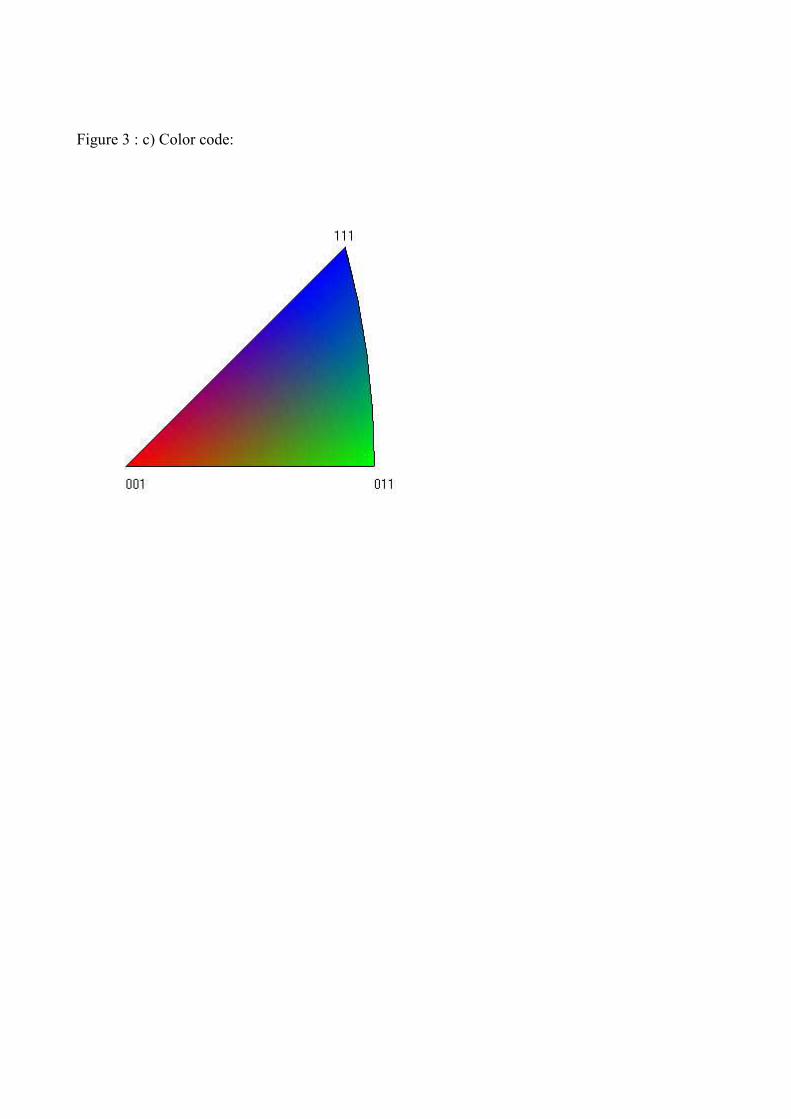
Figure 3 : c) Color code:
Figure 4 : Misorientation angle profiles of a scan along a line in a Silicon single crystal.
a) Camera length of 82mm.
0
0.05
0.1
0.15
0.2
0.25
0.3
0 100 200 300 400 500 600 700 800 900 1000
Distance to the first point [nm]
Misorientation [°]
82mm Kikuchi
82mm CBED
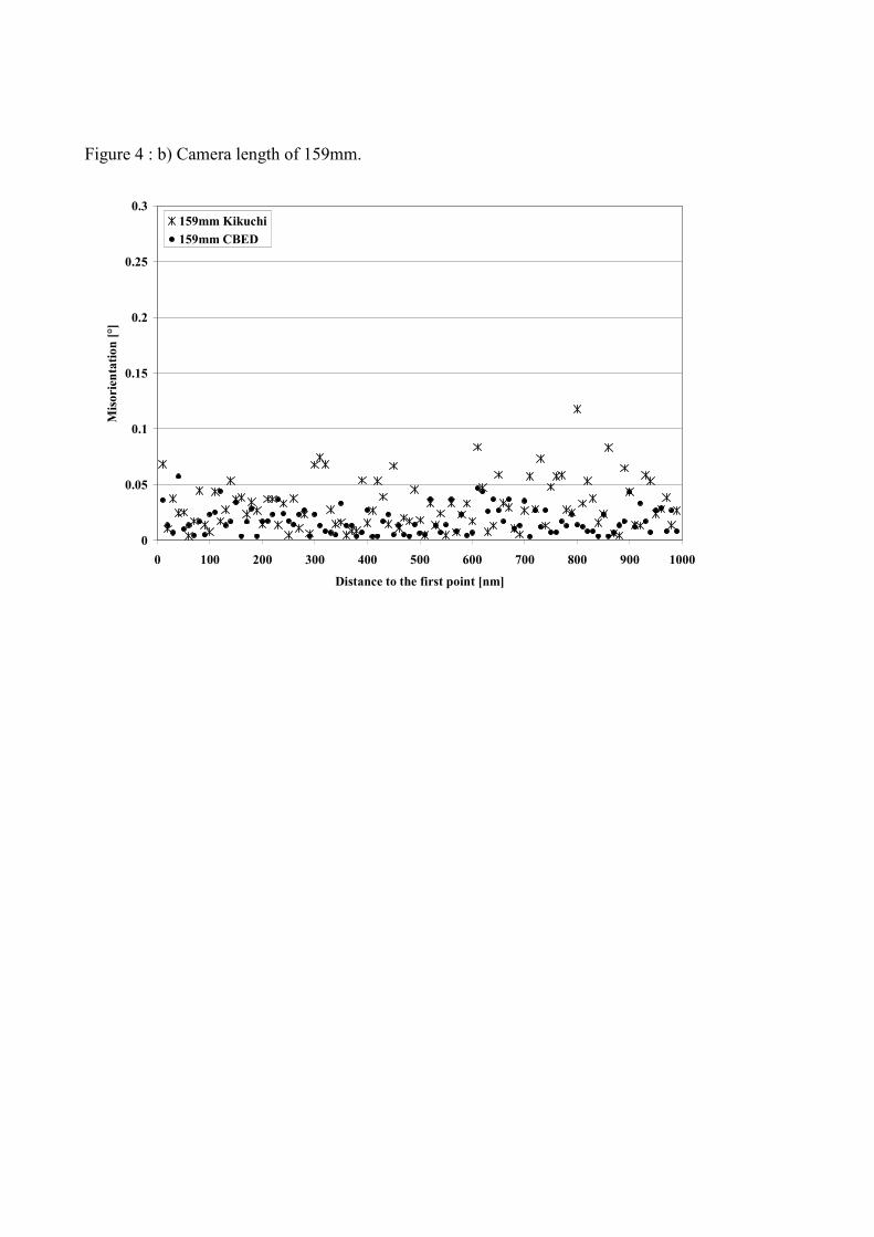
Figure 4 : b) Camera length of 159mm.
0
0.05
0.1
0.15
0.2
0.25
0.3
0 100 200 300 400 500 600 700 800 900 1000
Distance to the first point [nm]
Misorientation [°]
159mm Kikuchi
159mm CBED