pn diode characteristics mos capacitor mos transistoree143/fa10/lectures/lec_21.pdf · professor n...
TRANSCRIPT

Professor N Cheung, U.C. Berkeley
Lectre 21EE143 F2010
1
Microfabricationcontrols dopantconcentrationdistribution
ND(x) and NA(x)
Electron Concentration n(x)
Hole Concentration p(x)
Electrical resistivity
Sheet Resistance
Fermi level Ef (x) , Electric Field
PN Diode Characteristics
MOS Capacitor
MOS Transistor
Carrier Mobility

Professor N Cheung, U.C. Berkeley
Lectre 21EE143 F2010
2
Electron and Hole Concentrationsfor homogeneous semiconductor at thermal equilibrium
n: electron concentration (cm-3)p : hole concentration (cm-3)ND: donor concentration (cm-3)NA: acceptor concentration (cm-3)
1) Charge neutrality condition: ND + p = NA + n
2) Law of Mass Action : n p = ni2
Note: Carrier concentrations depend onNET dopant concentration (ND - NA) !
Assume completelyionized to form ND
+
and NA-

Professor N Cheung, U.C. Berkeley
Lectre 21EE143 F2010
3
How to find n, p when Na and Nd are known
n- p = Nd - Na (1)pn = ni2 (2)
(i) If Nd -Na > 10 ni : n Nd -Na(ii) If Na - Nd > 10 ni : p Na- Nd
* Either n or p will dominate for typical doping situations

Professor N Cheung, U.C. Berkeley
Lectre 21EE143 F2010
4
Probability of available states at energy E being occupiedf(E) = 1/ [ 1+ exp (E- Ef) / kT]where Ef is the Fermi energy and k = Boltzmann constant=8.617 10-5 eV/K
The Fermi-Dirac Distribution (Fermi Function)
T=0K
0.5
E -Ef
f(E)

Professor N Cheung, U.C. Berkeley
Lectre 21EE143 F2010
5
(2) Probability of available states at energy E NOT being occupied
1- f(E) = 1/ [ 1+ exp (Ef -E) / kT]
Properties of the Fermi-Dirac Distribution
(1) f(E) exp [- (E- Ef) / kT] for (E- Ef) > 3kT Note:At 300K,kT= 0.026eV•This approximation is called Boltzmann approximation
Probability
of electron state
at energy E
will be occupied
Professor N Cheung, U.C. Berkeley
Lectre 21EE143 F2010
6
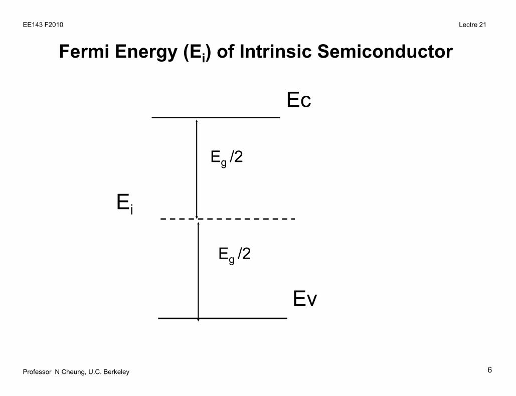
Fermi Energy (Ei) of Intrinsic Semiconductor
Ec
Ev
Ei
Eg /2
Eg /2
Professor N Cheung, U.C. Berkeley
Lectre 21EE143 F2010
7
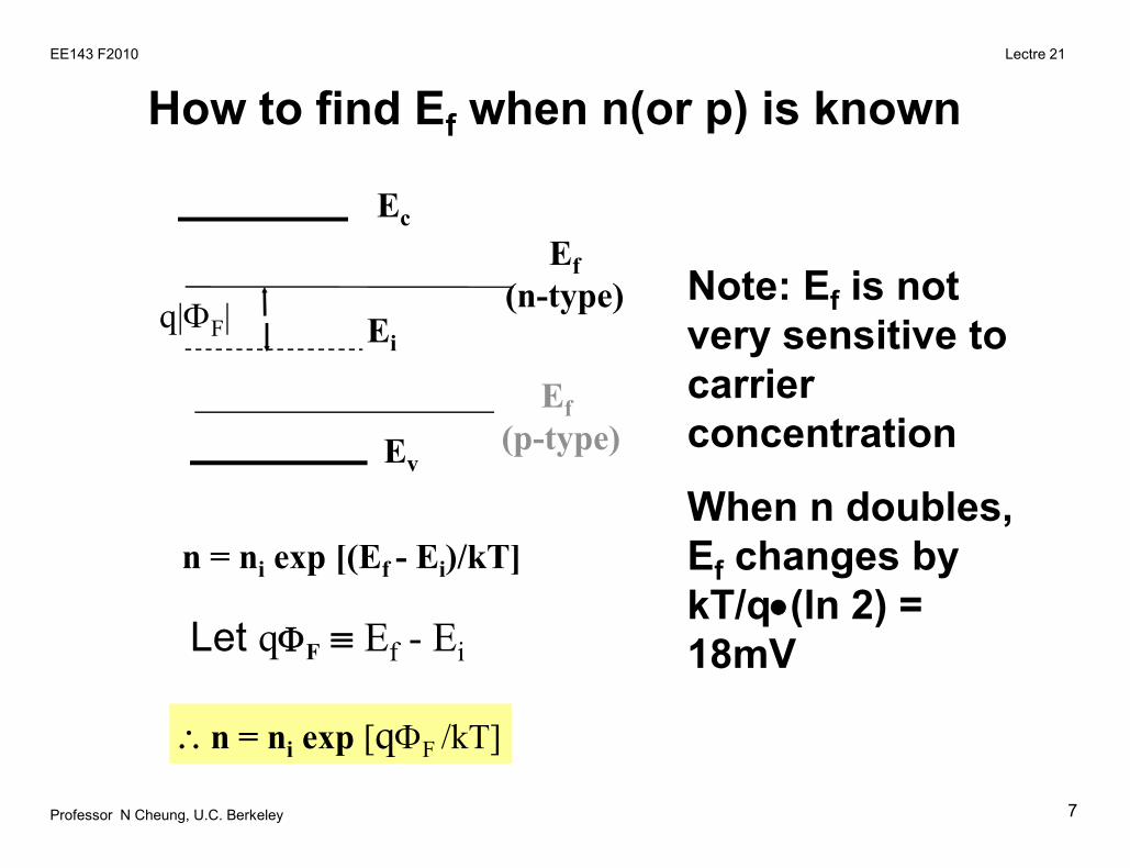
Ec
Ev
Ei
Ef(n-type)
Ef(p-type)
q|F|
Let qF Ef - Ei
n = ni exp [(Ef - Ei)/kT]
n = ni exp [qF /kT]
How to find Ef when n(or p) is known
Note: Ef is notvery sensitive tocarrierconcentration
When n doubles,Ef changes bykT/q(ln 2) =18mV

Professor N Cheung, U.C. Berkeley
Lectre 21EE143 F2010
8
Dependence of Fermi Level with Doping Concentration
Ei (EC+EV)/2 Middle of energy gap
When Si is undoped, Ef = Ei ; also n =p = ni

Professor N Cheung, U.C. Berkeley
Lectre 21EE143 F2010
9
Work Function of Materials
Eo
EV
ECq
SEMICONDUCTOR
Ef
Eo
Ef
METAL
Work function= q
Vacuumenergy level
qM is determined
by the metal materialqS is determined
by the semiconductor material,
the dopant type,
and doping concentration

Professor N Cheung, U.C. Berkeley
Lectre 21EE143 F2010
10
Work Function (qM) of MOS Gate MaterialsEo = vacuum energy level Ef = Fermi levelEC = bottom of conduction band EV = top of conductionband
Ef
Al = 4.1 eVTiSi2 = 4.6 eV
Ef
Eo
qM
Eo
qM
Ei
EC
EV
0.56eV
q = 4.15eV
0.56eV
q = 4.15eV (electron affinity)
Eo
Ei
EC
EV
0.56eV
q = 4.15eV
0.56eV
Ef
n+ poly-Si p+ poly-Si
qM

Professor N Cheung, U.C. Berkeley
Lectre 21EE143 F2010
11
Work Function of doped Si substrate
q = 4.15eV
Ef
Eo
qs
Ei
EC
EV
|q F|
0.56eV
0.56eV
* Depends on substrate concentration NB
Ef
Eo
qs
Ei
EC
EV
|qF|0.56eV
0.56eV
q = 4.15eV
n-type Si p-type Si
s (volts) = 4.15 +0.56 - |F| s (volts) = 4.15 +0.56 + |F|
i
BF n
NqkT ln
Professor N Cheung, U.C. Berkeley
Lectre 21EE143 F2010
12
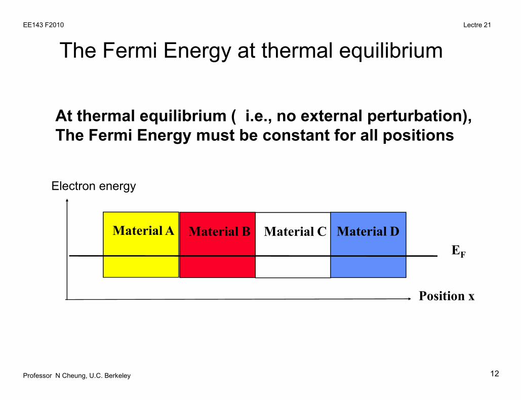
At thermal equilibrium ( i.e., no external perturbation),The Fermi Energy must be constant for all positions
The Fermi Energy at thermal equilibrium
Material A Material B Material C Material DEF
Position x
Electron energy

Professor N Cheung, U.C. Berkeley
Lectre 21EE143 F2010
13
Aftercontactformation
Beforecontactformation
Electron Transfer during contact formation
E
System 1 System 2
EF1
EF2e
System 1 System 2
EF
---
+++
E
System 1 System 2
EF1
EF2
e
System 1 System 2
EF
---
+++
Netnegativecharge
Netpositivecharge
Professor N Cheung, U.C. Berkeley
Lectre 21EE143 F2010
14
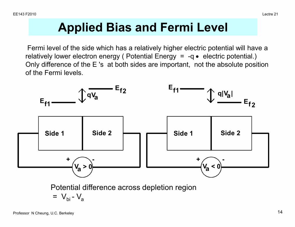
Fermi level of the side which has a relatively higher electric potential will have arelatively lower electron energy ( Potential Energy = -q electric potential.)Only difference of the E 's at both sides are important, not the absolute positionof the Fermi levels.
Side 2Side 1
Ef1
f2E
Va > 0
qVa Va
Side 2Side 1
Ef1
f2E
Va < 0
q| |
+ - -+
Potential difference across depletion region= Vbi - Va
Applied Bias and Fermi Level

Professor N Cheung, U.C. Berkeley
Lectre 21EE143 F2010
15
PN junctions
Complete Depletion Approximation used for charges inside depletion region(x) ND
+(x) – NA-(x)
n-Sip-Si
Depletion region
ND+ onlyNA
- only(x) is +(x) is -
ND+ and n
(x) is 0
NA- and p
(x) is 0
E-field
++
++
- -
- -Quasi-neutral
regionQuasi-neutral
region
n-Sip-Si
Depletion region
ND+ onlyNA
- only(x) is +(x) is -
ND+ and n
(x) is 0
NA- and p
(x) is 0
E-field
++
++
- -
- -Quasi-neutral
regionQuasi-neutral
region
http://jas.eng.buffalo.edu/education/pn/pnformation2/pnformation2.html
Thermal Equilibrium
Professor N Cheung, U.C. Berkeley
Lectre 21EE143 F2010
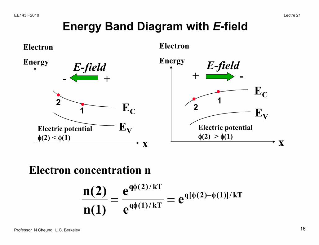
16
x
Electron
Energy E-field+-
EC
EV
21
x
Electron
Energy E-field+ -
EC
EV2
1
Electric potential(2) < (1)
Electric potential(2) > (1)
Energy Band Diagram with E-field
Electron concentration n
kT/)]1()2([qkT/)1(q
kT/)2(q
eee
)1(n)2(n

Professor N Cheung, U.C. Berkeley
Lectre 21EE143 F2010
17
1) Summation of all charges = 0
Electrostatics of Device Charges
x
Semiconductor(x)
xd1xd2
Semiconductor
-
-
x=0
p-typen-type
2) E-field =0 outside depletion regions
2 xd2 = 1 xd1
E = 0E = 0 E 0
Professor N Cheung, U.C. Berkeley
Lectre 21EE143 F2010
18
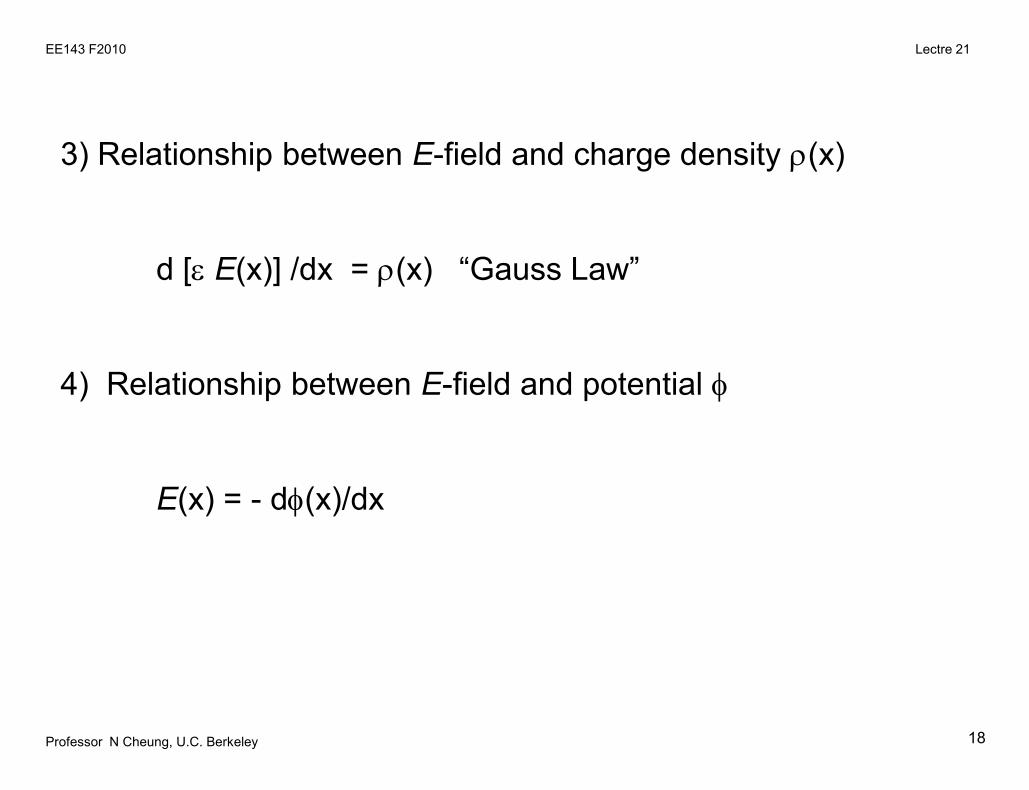
3) Relationship between E-field and charge density (x)
d [ E(x)] /dx = (x) “Gauss Law”
4) Relationship between E-field and potential
E(x) = - d(x)/dx

Professor N Cheung, U.C. Berkeley
Lectre 21EE143 F2010
19
Example Analysis : n+/ p-Si junction
x
-qNa
xd
x=0
+Q'
n+ Sip-Si
(x)
E (x)
xd
1) Q’ = qNaxd
3) Slope = qNa/s
4) Area under E-field curve= voltage across depletion region= qNaxd
2/2s
Emax =qNaxd/s
Depletionregion
2) E = 0
Depletion region
is very thin and is
approximated as
a thin sheet charge

Professor N Cheung, U.C. Berkeley
Lectre 21EE143 F2010
20
x
-
x=0
-qNA
+qND
(x)
-xp
+xn
x=0
x
1(x)
-xp
-qNA
Q=+qNAxp
x
x=0
2(x)
+qND
+xnQ=-qNAxp
Superposition Principle
If 1(x) E1(x) and V1(x)2(x) E2(x) and V2(x)
then1(x) + 2(x) E1(x) + E2(x) andV1(x) + V2(x)
+

Professor N Cheung, U.C. Berkeley
Lectre 21EE143 F2010
21
x
-
x=0
Slope =- qNA/s
E1(x)
-xp
x=0
x
1(x)
-xp
-qNA
Q=+qNAxp
x
x=0
2(x)
+qND
+xnQ=-qNAxp
+ x
-
x=0
+xn
E2(x)
Slope =+ qND/s

Professor N Cheung, U.C. Berkeley
Lectre 21EE143 F2010
22
x
-
x=0
Slope = - qNA/s
E(x) = E1(x)+ E2(x)
-xp +xn
Slope = + qND/s
Emax = - qNA xp /s= - qND xn /s
Sketch of E(x)
Professor N Cheung, U.C. Berkeley
Lectre 21EE143 F2010
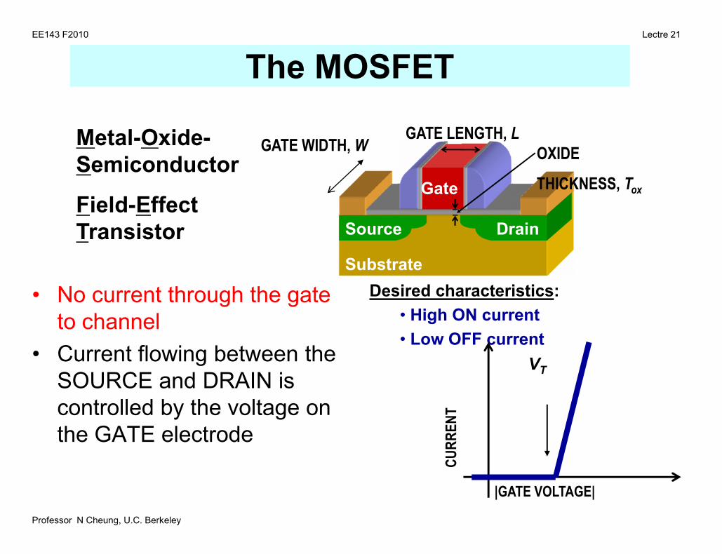
The MOSFET
• No current through the gateto channel
• Current flowing between theSOURCE and DRAIN iscontrolled by the voltage onthe GATE electrode
Desired characteristics:• High ON current• Low OFF current
|GATE VOLTAGE|
CURR
ENT
VT
Metal-Oxide-Semiconductor
Field-EffectTransistor
Substrate
Gate
Source Drain
GATE LENGTH, LOXIDE
THICKNESS, Tox
GATE WIDTH,W
Professor N Cheung, U.C. Berkeley
Lectre 21EE143 F2010
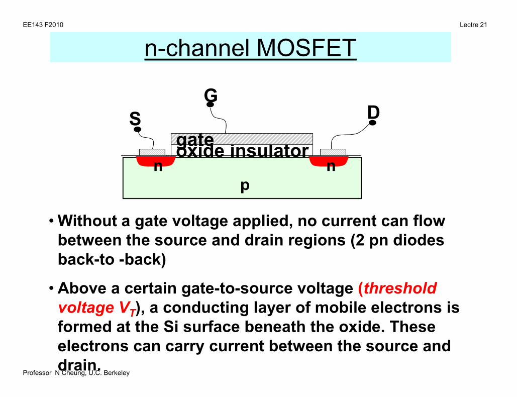
n-channel MOSFET
• Without a gate voltage applied, no current can flowbetween the source and drain regions (2 pn diodesback-to -back)
• Above a certain gate-to-source voltage (thresholdvoltage VT), a conducting layer of mobile electrons isformed at the Si surface beneath the oxide. Theseelectrons can carry current between the source anddrain.
np
oxide insulatorgaten
DSG

Professor N Cheung, U.C. Berkeley
Lectre 21EE143 F2010
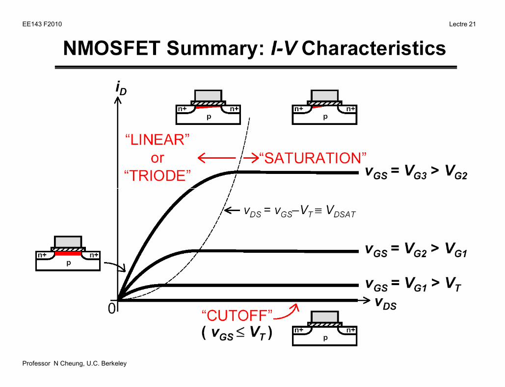
The MOSFET as a Controlled Resistor
• When VDS is low, ID increases linearly with VDS
ID
IDS = 0 if VGS < VT
VDS
VGS = 1 V > VT
VGS = 2 V
Inversion charge density Qi(x) = -Cox[ VGS – VT - V(x) ]
where Cox ox / tox.
Professor N Cheung, U.C. Berkeley
Lectre 21EE143 F2010
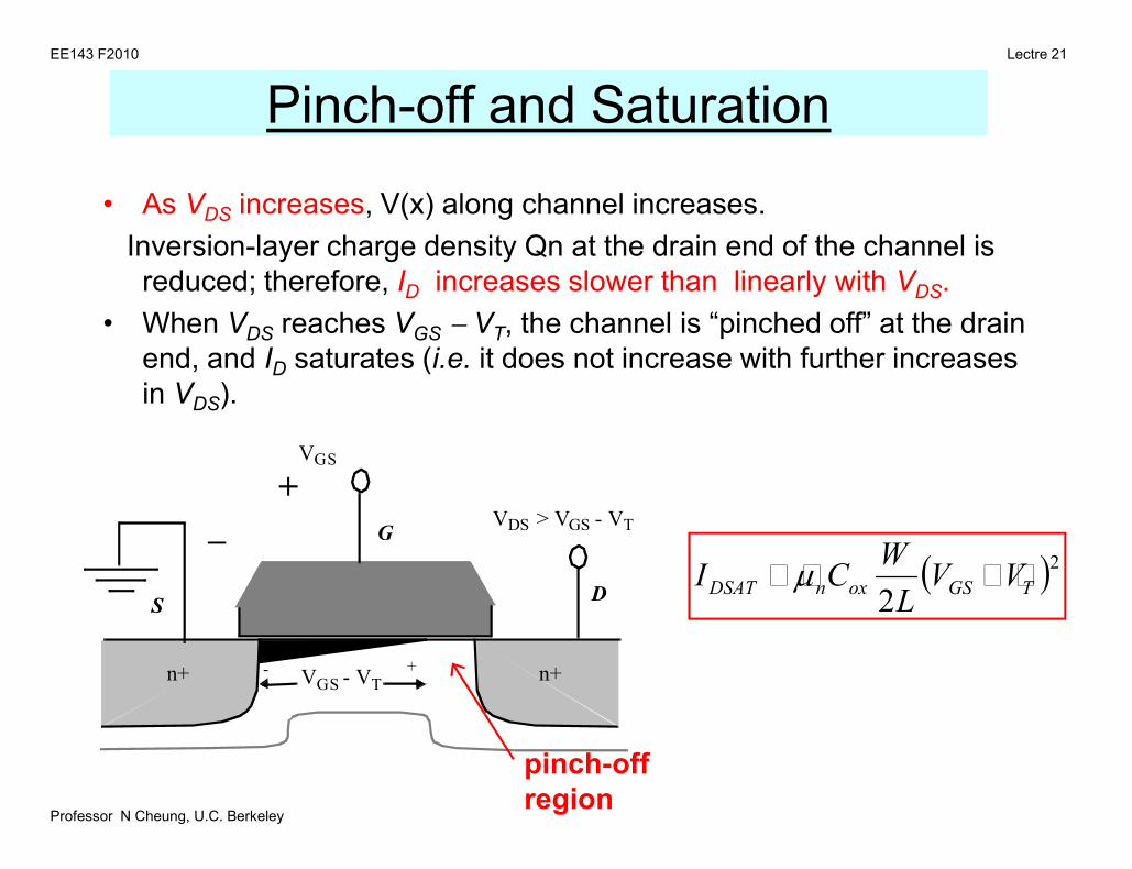
Pinch-off and Saturation
• As VDS increases, V(x) along channel increases.Inversion-layer charge density Qn at the drain end of the channel isreduced; therefore, ID increases slower than linearly with VDS.
• When VDS reaches VGS VT, the channel is “pinched off” at the drainend, and ID saturates (i.e. it does not increase with further increasesin VDS).
n+n+
S
G
VGS
D
VDS > VGS - VT
VGS - VT+-
pinch-offregion
+–
22 TGSoxnDSAT VVLWCI
Professor N Cheung, U.C. Berkeley
Lectre 21EE143 F2010
Professor N Cheung, U.C. Berkeley
Lectre 21EE143 F2010
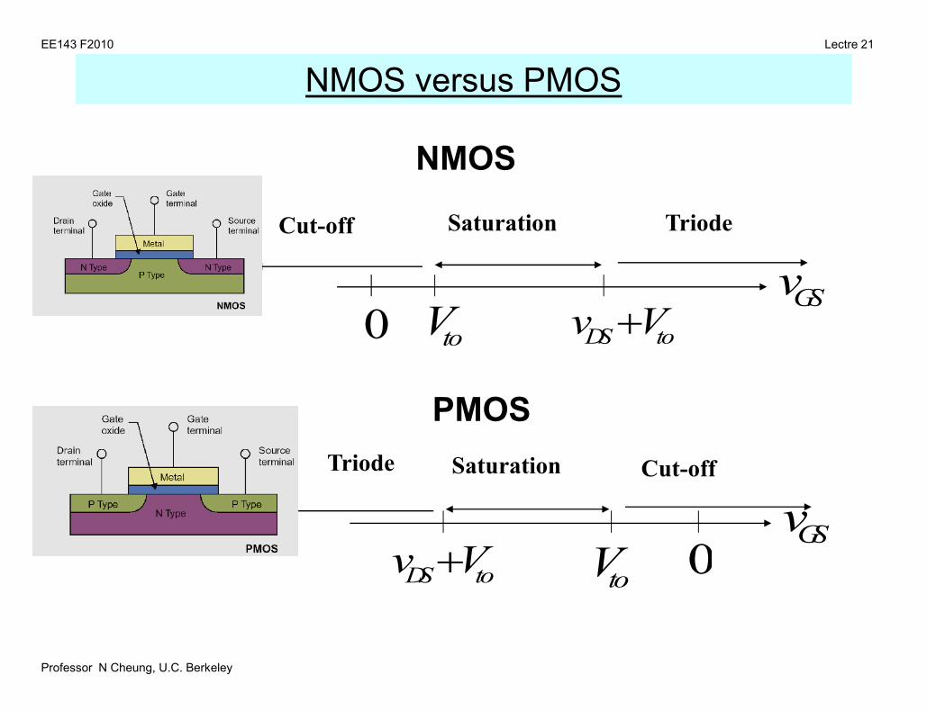
NMOS versus PMOS
DS tov V0GSv
TriodeSaturationCut-off
toV
NMOS
DS tov V 0GSv
Triode Saturation Cut-off
toV
PMOS

Professor N Cheung, U.C. Berkeley
Lectre 21EE143 F2010

Professor N Cheung, U.C. Berkeley
Lectre 21EE143 F2010

Professor N Cheung, U.C. Berkeley
Lectre 21EE143 F2010
IDsat Not proportional to
(VGS-Vt)2