pk2400 - pe2bz.philpem.me.uk
TRANSCRIPT

Users ManualRevision F
PK2400C-Programmable Controller

PK2400 Users ManualPart Number 019-0052
Revision F
Last revised on June 24, 2000 Printed in U.S.A.
Copyright© 1998 Z-World, Inc.
All rights reserved.
Z-World reserves the right to make changes and improvements to itsproducts without providing notice.
Trademarks Dynamic C
® is a trademark of Z-World, Inc.
Windows® is a trademark of Microsoft Corporation
PLCBus is a trademark of Z-World, Inc.
Hayes Smart Modem is a registered trademark of Hayes Microcomputer
Products, Inc.
Notice to UsersWhen a system failure may cause serious consequences, protecting lifeand property against such consequences with a backup system or safetydevice is essential. The buyer agrees that protection against conse-quences resulting from system failure is the buyers responsibility.
This device is not approved for life-support or medical systems.
All Z-World products are 100 percent functionally tested. Additionaltesting may include visual quality control inspections or mechanicaldefects analyzer inspections. Specifications are based on characterizationof tested sample units rather than testing over temperature and voltage ofeach unit. Z-World may qualify components to operate within a range ofparameters that is different than the manufacturers recommended range.This strategy is believed to be more economical and effective. Additionaltesting or burn-in of an individual unit is available by special arrangement.
Company Address
Z-World, Inc.2900 Spafford StreetDavis, California 95616-6800USA
Telephone:Facsimile:Web Site:
E-Mail:
(530) 757-3737(530) 753-5141http://www.z [email protected]

Table of Contents s iiiPK2400
TABLE OF CONTENTS
About This Manual vii
Chapter 1: Overview 11Introduction ......................................................................................... 12Processor Module ................................................................................ 12PK2400 Features ................................................................................... 13PK2410 Features ................................................................................... 13Options and Upgrades ......................................................................... 13Development Kit .................................................................................. 13System Development Programming Tools ............................................ 14Factory Upgrades ................................................................................ 14CE Compliance ..................................................................................... 15
Chapter 2: Getting Started 17Development Kit Packing List .............................................................. 18Connecting the PK2400 to a Host PC ................................................... 18Establishing Communication ................................................................ 20Steps to Run a Sample Program ........................................................... 20
Chapter 3: Subsystems 21Processor Module ................................................................................ 23
Interface Overview .......................................................................... 23Digital Input/Output ........................................................................ 23
Digital Inputs .............................................................................. 23Digital Outputs ........................................................................... 25Sourcing Driver .......................................................................... 26Sinking Drivers (Optional) .......................................................... 26Analog-to-Digital Converter ....................................................... 27
Extra Conversion .....................................................................28Voltage Reference ...................................................................28Data Conversion .....................................................................29Limitations on Output Range ..................................................29Low-Pass Filter .......................................................................29Internal Test Voltages .............................................................29Drift .........................................................................................30

iv s Table of Contents PK2400
Absolute Mode ......................................................................30Bipolar or Unipolar Conditioned Inputs .................................31Factory Gain and Bias Resistors .............................................31Initial Setup .............................................................................31
Representative Analog-to-Digital Setups ................................... 32Setting Up Conditioned Input .................................................... 32
Determine Bias Resistor To Center Span ................................34Unipolar Variation ...................................................................34Choose Best Standard Resistor Values ...................................34Bracketing Input Range ..........................................................34Pick Proper Tolerance .............................................................36Confirm Performance ...............................................................36Op-Amp Test Points ...............................................................37
Calibrating the Analog-to-Digital Converter ............................... 38Using Unconditioned Converter Channels ................................ 39Serial Communication Ports ........................................................ 41
RS-485 .....................................................................................41RS-232 and Programming Ports ...............................................42
Modem Communication .............................................................. 42Power-Supervisor Integrated Circuit .......................................... 43Real-Time Clock (RTC) ................................................................ 44
Relay Outputs ................................................................................. 44Keypad and Liquid Crystal Display ................................................ 46
Using the Keypad and Display .................................................. 46PK2400 Keypad .......................................................................... 46PK2400 Liquid Crystal Display ................................................... 48Bitmapped Graphics .................................................................... 48
Chapter 4: System Development 51Beginning Development ....................................................................... 52Operating Modes ................................................................................. 53
Program Mode ................................................................................ 53Run Mode ....................................................................................... 53
Developing with the RS-232 Port ......................................................... 53Developing with Serial Interface Board ................................................ 55Running a Program Standalone ........................................................... 56
Returning To Programming Mode ................................................... 56Developing an RS-485 Network ........................................................... 57

Table of Contents s vPK2400
Chapter 5: Software Reference 59Software Development Options ........................................................... 60
Dynamic C Development Software .................................................. 60Dynamic C Manuals ................................................................... 60Supplied Software ....................................................................... 60
Memory ................................................................................................ 61Flash EPROM Functions ................................................................. 61Nonvolatile Storage ......................................................................... 62
Digital Input and Output ...................................................................... 63Digital Input/Output Functions ....................................................... 63
Advanced Input/Output Programming ................................................ 66U2 (PIO No. 1) ................................................................................. 66U9 (PIO No. 2) ................................................................................. 66
Serial Communication Functions .......................................................... 67RS-485 Functions ............................................................................ 67
Analog-to-Digital Converter Drivers .................................................... 68Using the Liquid Crystal Display and Keypad ..................................... 69Real-Time Clock Integrated Circuit ....................................................... 76
Global Time and Date Structure ....................................................... 76Sample Programs .................................................................................. 78Additional Software ............................................................................. 78
Appendix A: Troubleshooting 79Out of the Box ...................................................................................... 80Dynamic C Will Not Start ..................................................................... 81Dynamic C Loses Serial Link ................................................................ 81PK2400 Repeatedly Resets ................................................................... 81Common Programming Errors ............................................................... 82
Appendix B: Specifications 83Specifications ....................................................................................... 84
Hardware Dimensions ..................................................................... 86Suggested Operating Temperature .................................................. 89Power ............................................................................................... 89Serial Interface Board ...................................................................... 89Jumper and Header Specifications .................................................. 90J12, RS-232, and RS-485 Ports ......................................................... 90Processor Module Jumpers ............................................................. 91Processor Module Gain and Bias Resistors .................................... 91
RS-232 Programming ............................................................................ 91

vi s Table of Contents PK2400
Appendix C: Power Management 93Direct Current Input ............................................................................. 94Power Regulator ................................................................................... 94Power Failure ........................................................................................ 94Power Failure Sequence of Events ....................................................... 95
Multiple Power-Line Fluctuations ................................................... 95Holdup Time .................................................................................... 96Recommended Power-Failure Routine ............................................. 97
Appendix D: Input / Output Map and Interrupt Vectors 99Memory Map ..................................................................................... 100Input / Output Map ............................................................................ 100Interrupt Vectors ................................................................................ 101Interrupt Priorities .............................................................................. 102
Appendix E: Serial Interface Board 103Features ............................................................................................. 104External Dimensions ........................................................................... 105
Appendix F: Battery 107Storage Conditions and Shelf Life ...................................................... 108Instructions for Replacing the Lithium Battery .................................. 108Battery Cautions ................................................................................ 109
Index 111
Keypad Template

About This Manual s viiPK2400
ABOUT THIS MANUAL
This manual provides instructions for installing, testing, configuring, andinterconnecting the Z-World PK2400 controller.
Instructions are also provided for using Dynamic C functions. CompleteC and Dynamic C references and programming resources are referencedwhen necessary.
AssumptionsAssumptions are made regarding the user's knowledge and experience inthe following areas.
Ability to design and engineer the target system that interfaces withthe PK2400.
Understanding of the basics of operating a software program andediting files under Windows on a PC.
Knowledge of the basics of C programming.
For a full treatment of C, refer to the following texts.
The C Programming Language by Kernighan and RitchieC: A Reference Manual by Harbison and Steel
Knowledge of basic Z80 assembly language and architecture.
For documentation from Zilog, refer to the following texts.
Z180 MPU User's ManualZ180 Serial Communication ControllersZ80 Microprocessor Family User's Manual
$
$
PK2400viii s About This Manual
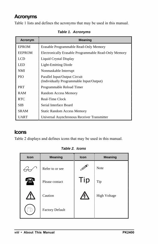
AcronymsTable 1 lists and defines the acronyms that may be used in this manual.
IconsTable 2 displays and defines icons that may be used in this manual.
Table 1. Acronyms
Acronym Meaning
EPROM Erasable Programmable Read-Only Memory
EEPROM Electronically Erasable Programmable Read-Only Memory
LCD Liquid Crystal Display
LED Light-Emitting Diode
NMI Nonmaskable Interrupt
PIO Parallel Input/Output Circuit(Individually Programmable Input/Output)
PRT Programmable Reload Timer
RAM Random Access Memory
RTC Real-Time Clock
SIB Serial Interface Board
SRAM Static Random Access Memory
UART Universal Asynchronous Receiver Transmitter
Table 2. Icons
Icon Meaning Icon Meaning
$ Refer to or see ! Note
( Please contact 7LS Tip
Caution High Voltage
)'
Factory Default

About This Manual s ixPK2400
ConventionsTable 3 lists and defines the typographic conventions that may be used inthis manual.
Pin Number 1A black square indicatespin 1 of all headers.
MeasurementsAll diagram and graphic measurements are in inches followed by millime-ters enclosed in parenthesis.
Table 3. Typographic Conventions
Example Description
while Courier font (bold) indicates a program, a fragment of aprogram, or a Dynamic C keyword or phrase.
// IN-01… Program comments are written in Courier font, plain face.
Italics Indicates that something should be typed instead of theitalicized words (e.g., in place of filename, type a file’sname).
Edit Sans serif font (bold) signifies a menu or menu selection.
. . . An ellipsis indicates that (1) irrelevant program text isomitted for brevity or that (2) preceding program text maybe repeated indefinitely.
[ ] Brackets in a C function’s definition or program segmentindicate that the enclosed directive is optional.
< > Angle brackets occasionally enclose classes of terms.
a | b | c A vertical bar indicates that a choice should be made fromamong the items listed.
J1Pin 1

PK2400x s About This Manual
This page is blank intentionally.

PK2400 Overview s 11
CHAPTER 1: OVERVIEW

PK240012 s Overview
IntroductionThe PK2400 consists of a processor module and a graphic liquid crystaldisplay (LCD) integrated with a front panel and an interface board. Theentire unit measures only 7.75" × 4.0" × 1.125". This slim package is idealfor an application that requires a powerful, compact controller with built-inoperator interface. The front panel has an overlay containing a displaywindow and a keypad for operator entry. The interface board contains theinput and output connectors and the circuitry to interface the controllerwith the keypad and the display.
The keypad hosts snap-dome membrane switches that provide the userwith tactile feedback. All keys are programmable, allowing the user tobuild a custom interface. The keypad legend and function key array canbe easily changed. The three soft function keys (softkeys) allow forinput to prompts on the LCD and are software programmable.
The PK2400's steel enclosure is a mylar-coated lexan front panel with heatreleasing top and bottom vents. The optional bezel gasket allows forwaterproof mounting; the panel mount is 1/16" to 1/8" thick.
Processor ModuleThe PK2400 processor module is a small, powerful board that is easilyprogrammed using Dynamic C. Moreover, the processor module offersimpressive processing power for a wide variety of control applications.
Real-time programs can be developed on any of the PK2400 series units inthe target system without the necessity of expensive in-circuit emulatorsor logic analyzers.
All PK2400s protect data in static RAM and the real-time clock's contents(PK2400 only) with a backup battery. The PK2400 has eight high-currentoutputs, two of which are used by the nonlatching relays.

PK2400 Overview s 13
PK2400 Features Nine protected digital inputs, pull-up and/or pull-down (-20 to +24 V)
Two conditioned analog inputs
Six high-current outputs
Two nonlatching relays (2 A at 30 V DC or 0.5 A at 120 V AC)
Built-in temperature sensor for sensing temperature near board
128 x 64 graphic LCD with software contrast control
Display backlight with software on/off
Keypad with 20 keys and 3 softkeys
RS-232 serial channel
RS-485 serial channel
Switching power supply
Buzzer
128K static RAM (SRAM)
128K flash EPROM
Real-time clock
PK2410 Features All features of the PK2400 except relays, thermistor, switching power
supply, analog inputs, and real-time clock
Two additional high-current outputs
Options and Upgrades Serial Interface Board (SIB) with programming cable
Aluminum bezel, includes gasket and mounting clips (8.5" × 4.75" ×0.125")
256K flash EPROM
Wall mount cold-rolled steel enclosure (7.85" × 4.1" × 1.5")
Development Kit User's technical reference manual with schematics
Power supply (AC adapter not in international kits)
Programming cable

PK240014 s Overview
System Development Programming ToolsApplication programs for the PK2400 are developed using Dynamic C,Z-World's real-time C language development tool. Dynamic C is a versionof the industry standard C programming language that has been optimizedfor development of real-time, multitasking control systems. Dynamic Cruns under Windows on an IBM PC or compatible. As an integratedsoftware-development system, Dynamic C provides an easy-to-use editor,compiler, and interactive debugger, which eliminate the need for expensivetest equipment like third-party debuggers or in-circuit emulators. DynamicC furnishes libraries of pre-written functions and software drivers thatmake software development fast and convenient.
When a program compiles, the host PC downloads the executable code,via the processor module's RS-232 port, directly to the onboard flashEPROM. This feature allows fast in-target development and debugging.
Another method for downloading programs from a host PC to a PK2400 isvia a Z-World Serial Interface Board (SIB). By using the optional SIB, theRS-232 port is left free for other applications.
The PK2400 supports up to 256K of electronically reprogrammable flashEPROM. Flash EPROM allows programs to be downloaded into nonvola-tile memory without using an EPROM burner.
Z-World's Dynamic C reference manuals provide completesoftware function descriptions and programming instructions.
Factory UpgradesIn large quantities, the PK2400 can be factory customized with one or twolatching relays. A latching relay replaces a nonlatching rely and uses anadditional high-current output. In other words, a latching relay uses twohigh-current outputs, and a nonlatching relay uses only one high-currentoutput.
Contact a Z-World Sales Representative for pricing information.
For ordering or customizing information, call a Z-World SalesRepresentative at (530) 757-3737.(
$

PK2400 Overview s 15
CE ComplianceThe PK2400 has been tested by an approved competentbody, and was found to be in conformity with applicable ENand equivalent standards. Note the following requirementsfor incorporating the PK2400 in your application to complywith CE requirements.
The power supply provided with the Development Kit is for develop-ment purposes only. It is the customers responsibility to provide aclean DC supply to the controller for all applications in end-products.
Fast transients/burst tests were not performed on this controller.Signal and process control lines longer than 3 m should be routed in aseparate shielded conduit.
The PK2400 has been tested to Light Industrial Immunity standards.Additional shielding or filtering may be required for an industrialenvironment.
Visit the Technical Reference pages of the Z-World Web siteat http://www.zworld.com for more information on shieldingand filtering.
$

PK240016 s Overview
This page is blank intentionally.

PK2400 Getting Started s 17
CHAPTER 2: GETTING STARTED
Chapter 2 provides instructions for connecting the PK2400 to a host PCand running a sample program.

PK240018 s Getting Started
Development Kit Packing ListThe Development Kit includes items necessary for PK2400 software andhardware development. The kit includes the following items:
Wall power supply (12 V DC) (not included in kits sold outside NorthAmerica)
Programming serial cable
A reference manual with schematics
Connecting the PK2400 to a Host PCThe PK2400 can be connected to a host PC via the J12 screw terminal stripor via Serial Interface Board (SIB). Although the ideal developmentmethod is with a SIB2, screws 9 through 13 on screw terminal strip J12comprise the PK2400s development serial terminal. When a SIB is used,J12 is available for user applications.
PK2400 connectors are individual screw terminals that are not polarized orkeyed. Carefully observe terminal identification and wire alignment beforemaking a connection and before applying power.
Using the programming cable provided in the development kit, connectthe PK2400 to a host PC with the following steps.
1. Disconnect power source to the PK2400.
2. Make sure a jumper is installed on pins 1 and 2 of header J1 on theprocessor module. The PK2400 is shipped with the requiredjumper factory-installed on pins 7 and 8 of header J1.
3. Connect the programming serial cable wires to screw terminal strip J12as described in Table 2-1 and shown in Figure 2-1. Use caution wheninserting wires into J12 and/or J13 in order to prevent short-circuitingthe board.
4. Connect the serial cables DE-9 connector to the host PC COM port.
5. Reconnect power source. The PK2400 is now in RS-232 programmingmode.
Caution: Hazardous voltage is present in the inverter circuit.

PK2400 Getting Started s 19
U7
to Keypad
PK2400 Rear View
Caution
J12
J13
to LCDJ7
battery
RT
SC
TS
\RD
at\T
Dat
Gnd
Table 2-1 lists connection points between the PK2400 and the host PC.
Figure 2-1 illustrates the location of screw terminal strip J12.
Figure 2-1. PK2400 Screw Terminal Strips
Because of the proximity of solder pins, use caution wheninserting wires into J12 and/or J13 in order to prevent a shortcircuit on the board.
Table 2-1. RS-232 Programming Cable Connections
PC PK2400
RS-232Signal
DE-9 PinNumber
SignalDirection
Serial CableWire Number Serial Cable
SignalJ12
ConnectionSignalName
DCD 1 ← 1 None nc —
DSR 6 ← 2 None nc —
RD 2 ← 3 TXD 11 \TDAT
RTS 7 → 4 CTS 13 CTS
SD 3 → 5 RXD 10 \RDAT
CTS 8 ← 6 RTS 12 RTS
DTR 4 → 7 None nc —
RI 9 ← 8 None nc —
SG 5 — 9 None 9 GND
Nomenclature
CTS Clear to SendDCD Data Carrier DetectDSR Data Set ReadyDTR Data Terminal ReadyRD Receive Data
RI Ring IndicatorRTS Request to SendSD Send DataSG Signal Groundnc no connection

PK240020 s Getting Started
Establishing CommunicationAfter hardware is connected, communication can be established betweena host PC and the PK2400. Establish communication by double-clickingthe Dynamic C icon to start the software.
Each time Dynamic C starts up, communication with thePK2400 is attempted.
If no error messages are displayed, communication has been successfullyestablished.
If an error message such as Target Not Responding orCommunication Error is shown, see Appendix A, Trouble-shooting.
After making the necessary changes to establish communication betweenthe host PC and the PK2400, use the Dynamic C shortcut <Ctrl Y> to resetthe controller and initialize communication.
Steps to Run a Sample Program1. Open the sample program DEMO_RT.C located in Dynamic C directory
Samples.
2. Compile the program by pressing F3 or by choosing Compile from theCompile menu. Dynamic C compiles and downloads the program intothe PK2400s flash memory.
During compilation, Dynamic C rapidly displays severalmessages in the compiling window. This condition is normal.
3. Run the program by pressing F9 or by choosing Run from the Runmenu.
If an error message such as Target Not Responding orCommunication Error is shown, see Appendix A, Trouble-shooting.
4. To halt the program execution, press <Ctrl Z>.
5. To restart program execution, press F9.
Programming with a SIB is described in Chapter 4, SystemDevelopment. The SIB is not included in the standardDevelopment Kit and must be purchased separately.
!
$
!
$
$

PK2400 Subsystems s 21
CHAPTER 3: SUBSYSTEMS

PK
24002
2 s
Su
bs
ys
tem
s
Backup Battery
“Data Bus”
Z180
Regulator DCIN
RS-232SerialChannel 0
RS-485SerialChannel 1
FlashEPROM
SRAM
Supervisor
Reset,PFI
ClockedSerial I/O
to SerialInterfaceBoard
PIO 1
A/D 2
4
8
RTC
Analog InputsTemperature Sensor
B
A
PIO 2 High-Current Output
KeypadLCD
Prot. Input 8
H.C. Driver4
2Relays
4
8
4
NO, COM, NC each
Prot. Input 0–3Prot. Input 4–7
2
Mux
A
ProcessorModule
Switching Reg.
Beeper
Logic
+5 V+5 V
Figure 3-1. PK2400 Block Diagram

PK2400 Subsystems s 23
Processor Module
Interface OverviewThe PK2400 uses a processor module as the brains of the system and asthe source for inputs and outputs. This section describes the resourcesprovided by the processor module and the interfaces between the PK2400main circuit board and that module. Figure 3-1 is a block diagram of thePK2400 system.
Digital Input/OutputThe module uses two Zilog PIO integrated circuits to provide digital I/Osignals. Some of the digital I/O signals are used in conjunction with thePK2400 main board to provide digital I/O to the user. Digital I/O softwaredrivers relieve the user from having to understand the details of program-ming the PIOs. The digital I/O signals are brought to the PK2400 mainboard via headers. The digital I/O signals are connected to protectioncircuits and high-pow drivers to provide improved I/O capability for thePK2400.
Digital InputsThe PK2400s nine protected digital inputs (Pin 00 through Pin 08) areflexible and robust.
High-voltage protection circuits allow the inputs to detect switch con-tacts, relay contacts, outputs from open-collector transistor devices,logic-level outputs, and high-voltage outputs. The protected digitalinputs have the following features:
Nominal input voltage range of 20 V to +24 V
Protection against overloads over the range of 48 V to +48 V
Logic-level detection
The nominal voltage range for the protected digital inputs is 20 V to+24 V. The inputs are protected against overvoltages in the range 48 Vto +48 V, but should not be regularly subjected to voltages outside thenominal voltage range.
Logic-level signals can be detected using any of the digital inputs. Thelogic threshold is nominally 2.5 V. The maximum guaranteed low voltage is1.25 V. The minimum guaranteed high voltage is 3.75 V.

PK240024 s Subsystems
The digital inputs may be pulled up to 5 V or down to ground. Theimpedance of the digital input lines is 4.7 kΩ over 0 to 5 V. Outside thisrange, the input impedance is greater than 3.9 kΩ. Figure 3-2 illustratesheader J4 pull-up and pull-down configurations. A jumper in position Aaffects protected inputs PIN0 through PIN3 on the J12 screw terminalstrip. Jumpers in position B affect protected input PIN4 on J12 and PIN5through PIN8 on the J13 screw terminal strip.
Figure 3-2. Digital Input Jumper Settings
High C
urrentO
utputs
J13
AGnd
/RDat
/TDat
RTS
CTS
Gnd
AD0
AD1
PIN2
PIN1
PIN0
485+
Gnd
PIN4PIN3
J12
485-
Out7
+5 V
Out6Out5
Out4
Out3
Out2
Out1
Out0
Gnd
K
DCIN
PIN7
PIN8
PIN6
PIN5
16 1
15 2
14 3
13 4
12 5
11 6
10 7
9 8
8 9
7 10
6 11
5 12
4 13
3 14
2 15
1 16
RS
-232P
rotectedInputs
ProtectedInputs
RS
-485
Pull-up configuration Pull-down configuration
1 2
3 4
J 4
5 65 6
1 2
3 4
J 4
5
A A BB
Analog

PK2400 Subsystems s 25
Figure 3-3 illustrates a typical digital input line.
Figure 3-3. Typical Digital Input
Digital OutputsThe PK2400s eight digital outputs (Out0 through Out7) provide high-voltage, high-current digital outputs. Two outputs repeat the condition ofthe nonlatching relays, and therefore are not independently usable. Seethe Relays section in this chapter for more information. Sourcing andoptional sinking drivers will drive a variety of loads, including inductiveloads such as relays, small solenoids, or stepping motors.
Figure 3-2 illustrates the location of the high-current digital output screwterminals on screw terminal strip J13.
Note the following points regarding the digital outputs:
Each output is individually addressable.
Each output includes a protective diode that returns inductivespikes to the power supply.
Sourcing drivers are standard. Sinking drivers are optional.
The total number of outputs that can be on simultaneously is subject tochip power limits and ambient temperature. There are power limitations oneach channel as well as on the entire driver chip. Eight channels (Out0through Out7) are driven by one driver chip.
0.01 µFRInputs 19
R = 22 kΩ+5 V
4.7 kΩ

PK240026 s Subsystems
InductiveLoad
P2A (07)
UDN2985A
K
J7
4
21
3
J7ExternalDirect Current
Out0 - Out7
Sourcing DriverFigure 3-4 illustrates the connection for the UDN2985A sourcing driver.
Note the following points regarding the UDN2985A sourcing driver:
Outputs pull high (source current) when turned on.
The chips rating is 30 V and 250 mA maximum per channel,subject to the chips thermal limits and ambient temperature.
With all channels on, each channel can source up to 170 mAcontinuously (100 percent duty cycle) as long as the chiptemperature is less or equal to 50°C. At 70°C the current must bereduced to 140 mA or less.
Figure 3-4. Sourcing Driver Configurations
Sinking Drivers (Optional)Figure 3-5 illustrates the configuration for the ULN2803 sinking driver:
Figure 3-5. Sinking Driver Configuration
InductiveLoad
P2A (07)
ULN2803
K
J7
4
2
1
3
J7
External Direct Current
Out0 - Out7

PK2400 Subsystems s 27
Note the following points regarding the ULN2803 sinking driver chip:
Outputs pull low (sink current) when turned on.
The chips rating is 48 V and 500 mA maximum per channel,subject to the chips thermal limits and ambient temperature.
With all channels on, each channel can sink up to 170 mAcontinuously (100 percent duty cycle) as long as the chiptemperature is less or equal to 50°C. At 70°C the current must bereduced to 140 mA or less.
Jumper J7 configures the outputs for either sourcing or sinking drivers.Figure 3-6 illustrates the J7 settings for sinking and sourcing drivers.
Figure 3-6. J7 Digital Output Jumper Settings
Use a series resistor to limit the in-rush current when drivingincandescent lamps.
See specifications section for more detailed information on thesinking and sourcing drivers.
Analog-to-Digital ConverterThe optional A/D converter is a 12-bit, serial-I/O, switched-capacitor,successive-approximation converter that can monitor temperature,measure position, or sense other types of analog signals. The A/Dconverter is onboard the processor module. The A/D converters internalmultiplexer samples and converts one input channel at a time.
The A/D converter provides four channels of 12-bit analog-to-digitalconversion. Two of the channels have op-amps for signal conditioningand two are unconditioned. The conditioned channels are brought out tothe PK2400 as analog inputs. One of the unconditioned channels is usedfor an onboard thermistor. The second unconditioned channel is con-nected to an onboard reference network.
Tip
$
34
Sourcing Drivers Sinking Drivers
12
J7 J7
34
12

PK240028 s Subsystems
Based on the A/D converters minimum conversion period, the maximumdata conversion rate is approximately 5,000 conversions per second. Theactual level of performance will be less because application programminghas a major effect on conversion rate.
Extra Conversion
The A/D converter sends converted data out serially, and receivescommands serially. During each serial-clock cycle, the chip shifts in onecommand bit and shifts out one data bit. This combined shifting accountsfor the devices behavior of returning a previous data reading automati-cally each time it accepts a conversion or configuration command.
The A/D converter communicates with the Z180 via data-input lineADDIN, the data-output line ADDOUT, the clock line ADCLK, the end-of-conversion line EOC, and the chip-select line /ADCS.
EOC goes to a logic 0 level during conversion, returning to 1 whenthe conversion is complete. Following the conversion period, the A/Dconverter shifts the resulting data one bit at a time over ADDOUT. Also,during each shift-clock period, the converter shifts in one bit of a com-mand word into the converter over ADDIN. This command word specifiesthe converters next operation. The PIOs ARDY line drives/ADCS. This line goes from a logic 1 to 0 during power-on initializa-tion as a result of putting Port A into Mode 3 operation. This transition isnecessary for the chip to function properly. Thereafter, the line is left low.
EOC comes in over PIO Port B data line 3 (P2B3), which also senses /NMI through the logic gate U7. (/NMI and EOC are not at a logic 0 levelat the same time and the driver software can distinguish between them incontext.)
Library routines take care of all the low-level details of communicationwith the A/D converter automatically.
Because the protocol for controlling the serial A/D converteris complex, Z-World strongly recommends using the libraryfunctions to control the converter instead of writing customfunctions.
Voltage Reference
The A/D converters two reference inputs, REF and REF+, establish thevoltage limits for analog inputs that produce the maximum and minimumconversion values. Inputs higher than REF+ return the maximum conver-sion value, and inputs less than REF return the minimum conversionvalue. The A/D converter has no out-of-range signal. Software will notbe able to distinguish between an input that is exactly at either limit of thevoltage range and one that exceeds the limits.
!

PK2400 Subsystems s 29
Data Conversion
The two conditioned inputs measure input signals over either a bipolar orunipolar voltage range. In either case, the operational amplifiers gain andbias resistors scale the signal ranges to conform to the 0 to 2.5 V inputrange of the A/D converter. Because of the inverting configuration of theop-amps, the maximum input voltage results in a minimum input voltage atthe converter.
The A/D converter determines a 12-bit digital value representing theconverted value of the input voltage. An input voltage at the A/Dintegrated circuit (equal to 0 V) converts to all zeros, and an input at 2.5 Vconverts as all ones. Dynamic C functions return 16-bit sign-extendedvalues. The functions return a reading appropriate to the unipolar orbipolar signals being measured, based on the arguments supplied to thefunction.
Limitations on Output Range
In actual practice, the op-amp outputs can only approach ground (0 V) butcannot actually reach it. The output low-voltage limit is about 10 mV to20 mV. The practical effect of this limitation is that approximately 0.4through 0.8 percent of the upper end of the input-signal range is unus-able. For example, if the input signal range is 0 to 10 V, the maximum usefulinput voltage is 0.02 to 9.96 V.
Low-Pass Filter
The 0.01 µF feedback capacitors in the op-amps circuits transform theop-amps into low-pass filters to attenuate any high-frequency noise thatmay be present in the signal. The filters characteristics depend on theresistors selected. Equation 3-1 illustrates how to calculate the 3-dBcorner frequency:
(3-1)
The 3-dB corner frequency, then, is 6715 kHz for this case with a gain of0.25 and a 1 percent feedback resistor of 2370 Ω.
Internal Test Voltages
By addressing virtual channels in the A/D converter, Dynamic Croutines can obtain internal test voltages from the A/D converter. How-ever, these readings measure VREF+ and VREF with respect to VREF andGND so that the resulting conversions are all zeros or all ones.
F01.0R21
fg
3dB µπ ××=

PK240030 s Subsystems
Drift
The AD680JT voltage reference exhibits a voltage drift of 10 ppm/°C(typical) to 30 ppm/°C (maximum). This drift corresponds to 25 to75 mV/°C or 1.75 to 5.25 mV over the temperature range of 0°C to 70°C.
The LMC662C operational amplifier exhibits an offset-voltage drift of1.3 mV/°C (typical), or 910 mV over temperature. A greater contribution tooverall drift arises from differences in the temperature coefficients of theuser-installed gain and bias resistors and the fixed 10 kΩ resistors R21through R24. Resistors R21 through R24 have temperature coefficients of±200 ppm/°C. Since the surface-mount resistors are close to each other,they are always at essentially the same temperature and their temperaturedeviations track closely.
Absolute Mode
The A/D converter operates in absolute mode. In absolute mode, the A/Dconverter compares the input signal against an accurate, stable, onboardreference. The onboard voltage-reference integrated circuit is an AD680JT,which has a drift specification of 10 ppm per °C typical.
The A/D converter is configured to operate in absolute-conversion modeusing an onboard voltage reference U4, as shown in Figure 3-7. REF ishard-wired to ground. REF+ connects to one of two sources of 2.5 V. TheA/D is factory-configured for absolute-conversion mode with REF+connected to a precision voltage reference, usually an AD680, U4 (butalternatively an LM385, U5).
Figure 3-7. Analog Reference in Absolute Conversion Mode
In
Out
GND
AD680JT
LM385-2.5
U5
R92.2 kΩ
+5V
U4
+5ANA
VREF
(Optional)
R1910 Ω
C30.1 µF

PK2400 Subsystems s 31
Bipolar or Unipolar Conditioned Inputs
Bipolar or unipolar signals can be measured using the two conditionedinputs.
Signals from sensors connected to AD0 and AD1 go to the inverting input ofone of two op-amps. The op-amps operate in the inverting configuration.User-selectable resistors R11 through R14 on the processor module set thegain and bias voltages of the am-plifiers. The 10 kΩ input and biasresistors R21 through R24 arefixed. Feedback capacitors C20and C21 roll off the high-fre-quency response of the amplifi-ers to attenuate noise.
Figure 3-8 illustrates the locationof the processor module condi-tioned analog input gain and biasresistors R11 through R14 .
Figure 3-8. Gain and Bias Resistors
Factory Gain and Bias Resistors
The A/D converter is configured with gain and bias resistors installed inthe conditioned A/D channels (configured for 0 V to 10 V direct currentinputs) so that the controller works right out of the box. If a differentinput voltage range is required, change the gain and bias resistors. SeeChapter 4 for information on accessing the processor module.
Initial Setup
The op-amps gain and bias resistors, R11 through R14, are installed insockets provided on the processor module.
RGAIN
, R11 and R13 = 2370 Ω
RBIAS
, R12 and R14 = 39.2 kΩ
Refer to sections under Setting Up Conditioned Input inthis chapter for a detailed method of determining the bestvalues for gain and bias resistors.
Resistors R11 through R14 yield a nominal gain of 0.25 volts for a unipolarinput-signal range of 0 to 10 volts. These values slightly differ fromtheoretical values. This discrepancy is derived from real-world resistortolerances.
Strip sockets with 0.300" centers accommodate one-eighth watt resistorsR11 through R14.
U9
H1R9
R10
U4
U5
R12 R14
R11 R13
Processor Module
PIO2
$

PK240032 s Subsystems
Representative Analog-to-Digital SetupsTable 3-1 gives the values of gain and bias resistors for various commoninput-voltage ranges in the absolute-conversion mode using the onboardvoltage reference. These values, which require standard one percentresistors, have been adjusted from theoretical values to account fortolerance variations. If none of these setups suits the application underdevelopment, proceed to the next section and follow the design methodpresented there to calculate the resistor values required.
In production quantities, the PK2400 can be ordered withsurface-mount resistors installed on the processor module inplace of the R11 through R14 resistors. Contact Z-World at(530) 757-3737 for details.
Setting Up Conditioned InputThe gain and bias resistors (R11 through R14) determine the input signalsvoltage relation to ground as well as its range. For example, assume acircuit must handle an input-signal range of 10 V spanning 5 V to +5 V.
Given this specification, select gain resistor RGAIN
(R11 or R13) to suit theinput-signal voltage range of 10 V.
!
Table 3-1. Gain and Bias Resistor Input Voltage Ranges
Input Range (V) Gain RGAIN (kΩ) RBIAS (kΩ)
-10.0 to +10.0 0.125 1.18 8.06
-5.0 to +5.0 0.250 2.37 6.65
-2.5 to +2.5 0.500 4.75 4.99
-2.0 to +2.0 0.625 5.90 4.53
-1.0 to +1.0 1.250 11.80 2.87
-0.5 to +0.5 2.500 23.70 1.69
-0.25 to +0.25 5.000 47.50 0.931
-0.10 to +0.10 12.500 1180.00 0.392
0 to +10.0 0.250 2.37 39.20
0 to +5.0 0.500 4.75 20.00
0 to +2.5 1.000 9.53 10.00
0 to +1.0 2.500 23.20 4.02

PK2400 Subsystems s 33
The gain of the amplifier is the ratio of its maximum output-voltage swingto the applications maximum input-voltage swing. The fixed 2.5 V inputrange of the A/D converter limits the op-amps output swings to 2.5 V.
Equation 3-2 expresses an amplifiers gain in terms of its input-voltagerange, where g is the gain, V
INMAX is the maximum input voltage, and
VINMIN
is the minimum input voltage.
(3-2)
The ratio of the user-specified gain resistor RGAIN
(R11 or R13) to its asso-ciated fixed-input resistor (R21 or R23) determines an amplifiers gain. Thegain for the amplifier in Figure 3-9 with its input resistor fixed at 10 kΩ is
Figure 3-9. Conditioned Analog Input Diagram
Given an input voltage range of 10 V, Equation (3-2) fixes the amplifiersgain at 0.25, and scales the input signals range correctly to the op-amps2.5 V max output range. R
GAIN must therefore be 2500 Ω.
MINMAX ININ VV
V2.5g
−=
000,10GAINR
g =
AN0 (U15-1),AN1 (U15-2)
AD0 (H1-20),AD1 (H1-18)
VREF (H1-17)
+
–
10 kΩ
10 kΩ
0.01 µF
R21,R23
R22,R24
C20, C21
R11, R13
R12, R14
RGAIN
RBIASVR0+,VR1+
VR0-,VR1-

PK240034 s Subsystems
Determine Bias Resistor To Center Span
If the op-amp is to servo its output properly around the desired centervoltage, establish the appropriate bias voltage at the op-amps non-inverting input. Select the bias, or offset, resistor R
BIAS (R12 or R14) to
position the input-voltage range correctly with respect to ground (in thisexample, -5 V to +5 V).
Because the value for RGAIN
has already been selected, the maximum inputvoltage (V
INMAX) determines the maximum input voltage seen at the
amplifiers summing junction (inverting input), circuit nodes VR0 andVR1. Compute VR0 or VR1 using Equation (3-3).
(3-3)
The bias voltage, VBIAS
, must equal its corresponding VRn- for each op-amp. A voltage divider consisting of a bias resistor, R
BIAS (R12 or R14),
and a fixed 10 kΩ resistor (R22 or R24) derives this bias voltage (VBIAS
=VR0+ or VR1+) from VREF, the 2.5 volt reference voltage.Equation (3-4) gives R
BIAS.
(3-4)
The 2.5 V term in the equations denominator is the reference voltage. Thelow-impedance voltage reference supplies this voltage in the absoluteconversion mode.
Unipolar Variation
Suppose the input range is 0 to +10 volts instead of 5 V to +5 V. VINMAXis now +10 V, V
BIAS becomes 2.0 V, and R
BIAS is 40 kΩ.
Choose Best Standard Resistor Values
Calculated values will not always be available as standard resistor values.In these cases, use the nearest standard resistor value. For example, use6650 Ω rather than 6667 Ω if using 1 percent resistors, or use 6800 Ω ifusing 5 percent resistors.
Bracketing Input Range
To be sure of accurately measuring signals at the extremes of an inputrange, be aware of the interaction between the 10 kΩ fixed resistors,R21 through R24, and the other installed resistors, R11 through R14. Inthe ideal case, the A/D converters input would be at the maximumexpected value of 2.5 volts if a signal is measured at the minimum inputlevel.
+
×=g1
gVVR
MAXIN0
BIAS
BIASBIAS V5.2
000,10VR
−×=

PK2400 Subsystems s 35
Resistor values vary within their rated tolerance bands. Thus, if the fixedinput resistor has less resistance than its nominal value and the installedresistor has a resistance slightly higher than its nominal value, the actualinput to the A/D converter would be more than 2.5 V. A loss of accuracythen results because the A/D input would reach its maximum input valuebefore the true signal input reaches the minimum expected input level.
Figure 3-10 illustrates how variations in tolerance can cause the analogsignal to exceed the limits of the analog converter.
Figure 3-10. Out of Range A/D Converter Input
Similarly, a deviation from nominal values in the bias network could skewthe A/D converters input voltage away from a theoretically computedvalue. For example, a small positive or negative deviation of the biasvoltage arising from variances in the resistive divider would offset theA/D converters input voltage. This offset would be positive or negative,tracking the deviations sign, and equal to the bias deviation multiplied bythe amplifiers gain plus one. Both of these effects could occur in thesame circuit.
0
10
2.5
PK2400 Input (V)
A/D
Con
vert
er In
put (
V)
A/D converter'sinput-voltagelimit
Op-amp output-voltagedeviation arising fromresistor variations
Out of range
Out of range

PK240036 s Subsystems
Pick Proper Tolerance
Use care when compensating for any discovered discrepancies. Forexample, if standard 5 percent resistors are used for R11 through R14,recall that resistor values are spaced approximately 10 percent apart.
Thee tolerance is ± 5 percent; therefore, any value calculatedwill be within ± 5 percent of a standard value.
If a gain is too high by just a small amount, then going to the next smalleststandard 5 percent value could result in a decrease in gain approaching 10percent. The same caveat applies to the bias network. Use 1 percentresistors to get a more precise choice of values.
Use the mathematically derived values if the loss of signalrange is acceptable.
Figure 3-11 illustrates the result of adjusting the resistor values so thatinput to the A/D converter stays within its specified 2.5 V range.
Figure 3-11. Converter Input Within A/D Range
Confirm PerformanceIf measurements are critical, check setups after installing resistors bymeasuring test signals at and near the input-voltage limits. See if voltagesfall within the A/D converters input range or if loss of accuracy occursbecause of over-excursions at the A/D converters input. Alternatively,measure the resistance of the factory-installed fixed resistors beforeselecting and measuring new resistors accordingly.
0 10
2.5
PK2400 Input (V)
A/D
Con
vert
er In
put (
V)
A/D converter'sinput-voltagelimit
Op-amp output-voltagedeviation arising fromresistor variations
!
!

PK2400 Subsystems s 37
Fixed resistors can be measured indirectly after installing resistors bymeasuring the voltages at the amplifiers inputs and outputs. UsingChannel 0 as an example, ground the input AD0 at pin 20 of H1. Thenmeasure the voltages at VR0 and the amplifiers output. Because thecurrents through the input resistor and the feedback resistor are essen-tially identical, the ratio of the voltages across the resistors is equivalentto the ratio of the resistors. Therefore, the gain is as displayed in Equa-tion (3-5):
(3-5)
Again using Channel 0 as an example, measure the voltage of VREF andthe voltage at VR0+ as displayed in Figure 3-12. Because the current intothe op-amp input is negligible, the resistance ratio of the two resistors inthe voltage divider alone determines VR0. Once both the value of theinstalled resistor and the value of VR0+ are known, compute the value of
the fixed resistor in the divider.
Figure 3-12. Voltage Test Points
Op-Amp Test Points
The factory-installed fixed resistorshave a 1 percent tolerance. Figure 3-13shows convenient points on the pro-cessor module to make voltage mea-surements of the op-amps circuitry.
−−−
=0
0
VR
VRVgain OUT
AIN0 (U15-1),AIN1 (U15-2)
AD0 (H1-20),AD1 (H1-18)
VREF (H1-17)
+
–
10 kΩ
10 kΩ
0.01 µF
R21,R23
R22,R24
C20, C21
R11, R13
R12, R14
RGAIN
RBIASVR0+,VR1+
VR0-,VR1-
R11 R13
R12
AIN0 VR1-
AIN1
R14 GND
VR0-
VR0+
GND VR1+
Figure 3-13. Analog Input Test Points

PK240038 s Subsystems
Calibrating the Analog-to-Digital ConverterThe inherent component-to-component variations of 5 or 1 percentresistors can swamp the 0.25 percent resolution of the A/D converter.To achieve the highest accuracy possible, calibrate the analog inputs.
The software drivers for the A/D converter provide routines to computecalibration coefficients (given two reference points) and store them in adefined location in nonvolatile memory. Each reference point is comprisedfrom the following pair of values:
Actual applied test voltage
Raw converted A/D value (a 12-bit integer)
The supplied Z-World A/D software library EZIOCMMN.LIB automaticallyuses these coefficients to correct all subsequent A/D readings.
The A/D converter functions are described in Chapter 5,Software Reference.
Table 3-2 lists the addresses in simulated EEPROM where the calibrationconstants are stored.
$
Table 3-2. A/D Converter Calbration Constants
Address in Simulated EEPROM A/D Channel
10–15 0
16–21 1
22–27 2
28–33 3

PK2400 Subsystems s 39
AGND
+5 V
A/D 2
10 kΩ
4.99 kΩ
330 Ω
AGND
+5 V
A/D 3
10 kΩ
330 Ω
T
Processor Module
PK2400
H1
- 16
H1
- 15
Using Unconditioned Converter ChannelsTwo additional input channels of the A/D converter are connected to anonboard thermistor and reference network as shown in Figure 3-14. Thethermistor and reference resistor can be used to measure the onboardtemperature.
Figure 3-14. Thermistor Circuit

PK240040 s Subsystems
Table 3-3 lists the Z-World thermistor outputs as a function of temperature.
Table 3-3. Temperature to Ohms Conversion Table
° C ° F Ω ° C ° F Ω
-70 -94 3,095,611 45 113 4,366
-65 -85 2,064,919 50 122 3,601
-60 -76 1,397,935 55 131 2,985
-55 -67 959,789 60 140 2,487
-50 -58 667,828 65 149 2,082
-45 -49 470,609 70 158 1,751
-40 -40 335,671 75 167 1,480
-35 -31 242,195 80 176 1,256
-30 -22 176,683 85 185 1,070
-25 -13 130,243 90 194 916
-20 -4 96,974 95 203 787
-15 5 72,895 100 212 678.6
-10 14 55,298 105 221 587.3
-5 23 42,314 110 230 510.1
0 32 32,650 115 239 444.5
5 41 25,395 120 248 388.6
10 50 19,903 125 257 340.8
15 59 15,714 130 266 299.8
20 68 12,493 135 275 264.5
25 77 10,000 140 284 234.1
30 86 8,056 145 293 207.7
35 95 6,530 150 302 184.8
40 104 5,324

PK2400 Subsystems s 41
Serial Communication PortsTwo Z180 serial ports support asynchronous communication at baud ratesfrom 300 to 57,600 bits per second.
1. Port 0 is a 5-wire RS-232 port (with RTS and CTS).
2. Port 1 is a half-duplex RS-485 port, which provides half-duplexasynchronous communication over twisted pair wires to adistance of up to 4 kilometers.
Figure 3-15 illustrates the configuration of Port 0 and Port 1.
Figure 3-15. Serial Communication Port Configuration
RS-485
The processor module has a half-duplex RS-485 serial channel that isbrought out to the screw terminal strips. The RS-485 signals are on screwterminal strip J12, screw terminal 2 (RS-485) and screw terminal 3(RS-485+). Figure 3-16 illustrates the RS-485 connections.
Figure 3-16. J12 RS-485 Connections
CTS
RTS
/RDAT
/TDAT
CTS
RTS
/RDAT
/TDAT
RS485–
RS485+TXD1
/CTS0
RXD1
TXD1
RXD0
TXD0
Z180
U10
/CTS0
/RTS0
RXD0
TXD0
/RTS0
U13 RS485–
RS485+
RXD1
EN485
PIO1 (P1B1)
3
5 H2
6
4
23 H324
J12
Processor Module
J12
16151413121110987654321
ProtectedInputs
RS-485
AG
nd
/RD
at
/TD
atR
TS
CT
S
Gnd
AD
0A
D1
PIN
2P
IN1
PIN
048
5+
Gnd
PIN
4P
IN3
485-
RS-232 Analog

PK240042 s Subsystems
RS-232 and Programming Ports
A five-wire RS-232 interface can be used either for programming or by anapplication. The RS-232 signals are on PK2400 screw terminal strip J12,screws 10 through 13 (the fifth wire goes to a ground). The PK2400 canalso be programmed without using the RS-232 port. Connecting aZ-World Serial Interface Board (SIB) leaves the RS-232 interface availableto an application during development.
See Z-Worlds Dynamic C manuals for specifics on modemcommunication software.
The PK2400s RS-232 support library is EZIOPK24.LIB. Support for serialcommunication includes the following functions:
Initializing the serial ports
Monitoring and reading a private circular receive buffer
Monitoring and writing to a private circular transmit buffer
CTS (clear to send) and RTS (request to send) control
XMODEM protocol for downloading and uploading data
A modem option
An echo option
Modem CommunicationModems and telephone lines allow RS-232 communication across greatdistances. With a modem, character streams that are read from the receivebuffer are automatically scanned for modem commands. The RS-232library supports communication with a Hayes Smart Modem or compat-ible. If the modem used is not truly Hayes Smart Modem compatible, theCTS, RTS, and DTR lines on the modem side must be tied together. TheCTS and RTS lines on the PK2400 side also have to be tied together. ANULL connection is also required for the TX and RX lines. A commercialNULL modem would already have its CTS and RTS lines tied together onboth sides.
The PK2400 supports the XMODEM protocol for downloading anduploading data. Currently, the library supports downloading an array ofdata that is a multiple of 128 bytes.
Uploaded data is written to a specified area in RAM. The targeted writingarea should not conflict with the current resident program or data.
Character echo is automatically suspended during XMODEM transfer.
See Z-Worlds Dynamic C manuals for specifics on modemcommunication software.
$
$

PK2400 Subsystems s 43
Power-Supervisor Integrated CircuitThe power-supervisor integrated circuit is a key component that helps asystem survive power fluctuations and power outages. Several vitalservices provided by the power supervisor are described in the followinglist.
Power-on resetThe supervisor integrated circuit generates the power-on reset for thePK2400 by holding /RESET low until the chip senses that VCC has risenabove reset threshold (»4.65 V) 4.65 V and battery voltage (2.5 V to 4.25 VDC). Also, when VCC falls below threshold, the supervisor integratedcircuit disables the RAM to prevent spurious writing of data.
RAM protectionThe power supervisor integrated circuit gates the decoded RAM-selectline to the RAMs chip-enable line whenever VCC is above the resetthreshold and VBAT. When VCC falls below the threshold, the ADM691de-asserts the chip-enable to prevent spurious writing to the RAM.
Watchdog timerThe watchdog timer cannot be disabled. The watchdog timer guardsagainst system or software faults. If an application program does nothit the watchdog timer at least every 1.0 second, the watchdog timerresets the Z180. The supervisors watchdog output (/WDO) connects tothe Z180s /INT1 interrupt line. /WDO is at logic zero level after a watch-dog reset and a logic 1 after a power-on reset.
To hit the watchdog timer, make a call to the library functionhitwd. This call makes a dummy one-byte DMA transfer viaDMA channel 1, which activates the DMA-end signal, /TEND1, hitting the watchdog timer.
Nonmaskable interruptThe supervisor integrated circuit generates a non-maskable interrupt(/NMI) from its power-fail output (/PFO) for the microprocessor if theunregulated direct current input (normally 9 V to 12 V DC) falls below7.9 V. This gives the PK2400 advanced warning of an impending powerfailure, so that it can execute shutdown routines.
R16 introduces approximately 830 mV of hysteresis into the supervisorICs sensing of the raw direct current, preventing noise on DCIN fromgenerating repeated interrupts when the input voltage is low. /NMI alsoconnects to port B (bit 3), of PIO2 (via IC U7B) to allow software tomonitor /NMI line after the non-maskable interrupt, and recover fromtemporary low-input voltage conditions or brownouts.
!

PK240044 s Subsystems
Backup-battery switchoverThe supervisor integrated circuit switches the RAM over to battery powerif VCC falls below the battery voltage VBAT (2.5 V to 4.25 V DC).
Real-Time Clock (RTC)The PK2400 processor module has an RTC on board. The RTC providestime and date functions plus 31 bytes of scratchpad RAM. The RTC alsohas the following features:
Automatically adjusts the last date of the month for the number ofdays in a month and accounts for leap years.
Reports time in either 24- or 12-hour format (with an a.m. or p.m.indication).
An external battery (2.5 V to 4.25 V DC) allows the integratedcircuit to retain its time and data when power fails.
Relay OutputsThe PK2400 has two nonlatching SPDT relay outputs capable of drivinghigh-current loads. These outputs are illustrated in Figure 3-17.
The relay outputs are available to the user on screw terminal strip J11.
Figure 3-17. Nonlatching Relay
The relays can handle maximum load currents up to 2 A. There is a 2.5 Afuse between the common connection and the terminal to prevent damagefrom over-current. Each contact on the relays also has a snubber (resistorand capacitor) circuit to help protect the contacts from arcing.
For CE compliance, the maximum switching voltage is lessthan 50 V AC or 75 V DC.
2
3
4
7
9
8
1
10
5
6
to PA4 or PA5
Non-Latching Relays
NC
COM
NO
!

PK2400 Subsystems s 45
An appropriately rated varistor must be connected at the load if highlyinductive loads are connected to the PK2400 relays. Switching off highlyinductive loads without the use of a varistor may damage the snubbercircuit and the relay. Installing the varistor in parallel with the snubberinstead of across the load may result in unintentional energizing of theload if the varistor fails in shorted condition. If the varistor installedacross the load fails in the shorted condition, the fuse will open and theload will not be energized.
Table 3-4 lists the terminal relay connections.
Figure 3-18 illustrates the location of screw terminal strip J11.
Figure 3-18. J11 Screw Terminal Strip Location
Table 3-4. 23-Key Keypad Connections
J11 TerminalNumber
Relay 2Connection
J11 TerminalNumber
Relay 1Connection
1 Normally open 4 Normally open
2 Common 5 Common
3 Normally closed 6 Normally closed
U7
2NO
2NC
1CO2NO
2CO
1NO
Caution
battery
J11
J12
J13
to LCD
aperturefor SIB
connector
J7

PK240046 s Subsystems
m 7 8 9
i 4 5 6
f 1 2 3
. 0 ?0.525
0.525
0.525
0.4
0.4
0.5
0.4
0.775
2.65
3.625
Keypad and Liquid Crystal DisplayThe PK2400 supports operator input/output through the keypad and theLCD. Features include a 128 column by 64 row backlit graphic LCDmodule and a 4 row by 5 column keypad with three additional soft keys.
The graphic LCD has software controllable electroluminescent backlight-ing installed as a standard feature. The keypad connects through con-nector J-2.
Using the Keypad and DisplayThe PK2400 keypad and display are supported by a large number ofsoftware drivers. The keypad and display can be used for a variety of userinterface applications, for example:
User code or password entry
System status display
Multiple language/character-set displays
Parameter monitoring and adjustment
Because the three function keys are close to the LCD screen, it is possibleto program on-screen prompts that correspond to the adjacent key.
PK2400 KeypadThe keypad is designed to accept a paper insert. Inserts can be customizedby photocopying the keypad template located behind the Schematic sec-tion in this manual.Figure 3-19 providesmeasurements for thekeypad template. All di-mensions are in inches.Inserts can be securedby taping the portion ofthe insert that extendsbeyond the keypad tothe supporting bracket.
Figure 3-19. 4 x 5 Plus 3 Keypad Default Legend

PK2400 Subsystems s 47
Figure 3-20 illustrates the keypad connections in Table 3-5.
Figure 3-20. Keypad Key Numbers
NOTE: Keys are numbered for orientation. They do not come labeled.
8
9
4
5 11
2
3
0
1
10
12
20
20
13
17
18
25
26
21
28
19
24
27
Table 3-5. 23-Key Keypad Connections
Key Connection Key Connection
0 R0, C0 16 R2, C0
1 R0, C1 17 R2, C1
2 R0, C2 18 R2, C2
3 R0, C3 19 R2, C3
4 R0, C4 20 R2, C4
5 R0, C5 21 R2, C5
8 R1, C0 24 R3, C0
9 R1, C1 25 R3, C1
10 R1, C2 26 R3, C2
11 R1, C3 27 R3, C3
12 R1, C4 28 R3, C4
13 R1, C5

PK240048 s Subsystems
PK2400 Liquid Crystal DisplayThe PK2400 LCD is easy to use with Dynamic C software libraries.Several of the Dynamic C graphic library functions return the operatingstatus of the LCD. The LCD status bits are shown in the followingdiagram.
BUSY - Reading a 1 indicates LCD is performing an operation. Readinga 0 indicates the LCD is ready to accept more data.
ON/OFF - When the ON/OFF bit is set (1) the display is on, any image onthe screen will be visible. When the bit is reset (0) any images on thedisplay will not be visible. The image is still in the display memory.
RESET - Resets the LCD module when low (0).
Bitmapped GraphicsMany of the Dynamic C functions that operate on the graphic LCD usebitmaps. These bitmaps represent the images on a section of the display.Each dot, or pixel, is represented by one bit in the bitmap. If the pixel ison, the corresponding bit is set. If the pixel is off, the corresponding pixelis reset.
The image on the display is two dimensional (width and height). Thebitmap used to store that display information is a one-dimensional array.Two-dimensional images are stored in column major, byte-aligned bitmapformat. Figure 3-21 illustrates the two-dimensional graphic coordinatesystem.
Figure 3-21. 64 x 28 Graphic Coordinates
7 6 5 4 3 2 1 0
BUSY 0 ON/OFF RESET 0 0 0 0Most significant bit Least significant bit
0,0
Graphic Coordinate System
0,6363,127
0,127

PK2400 Subsystems s 49
Column major means that bits are stored in the bitmap column by column.The first pixel of the first column (row 0, column 0) of the image is storedin the first bit position in the bitmap. The second pixel in the first columnis stored in the second bit position in the bitmap and so on. When theentire first column is stored in the bitmap, the process begins again withthe second column and repeats until all of the columns of the image arestored.
Byte aligned means that a column data will end on a byte boundary. If acolumn has a number of bits that is not evenly divisible by eight, then theremaining bits of the last byte representing a column will be left unused.Image data from the next column will be stored starting in the next byte.

PK240050 s Subsystems
This page is blank intentionally.

PK2400 System Development s 51
CHAPTER 4: SYSTEM DEVELOPMENT
Chapter 4 describes how to use and/or implement features of the PK2400series controller.

PK240052 s System Development
Beginning DevelopmentBefore beginning development, check the following items:
Verify that the PK2400 runs in standalone mode before connecting anyI/O devices.
Verify that the entire host system has good, low-impedance, separategrounds for analog and digital signals. Often the PK2400 is connectedbetween the host PC and another device. Any differences in groundpotential from unit to unit can cause serious problems that are hard todiagnose.
Verify that the host PCs COM port works by connecting a good serialdevice to the COM port. Remember that on a PC, COM1/COM3 andCOM2/COM4 share interrupts. User shells and mouse drivers, inparticular, often interfere with proper COM port operation. Forexample, a mouse running on COM1 can preclude running Dynamic Con COM3.
Use the supplied Z-World cables. The most common fault of user-made cables is failure to properly assert CTS at the RS-232 port of thePK2400. Without CTSs being asserted, the PK2400s RS-232 port willnot transmit. Assert CTS by either connecting the RTS signal of thePCs COM port or looping back the PK2400s RTS.
Experiment with each peripheral device connected to the PK2400 inorder to determine how it appears to the PK2400 when powered up,powered down, and/or when its connecting wiring is open or shorted.

PK2400 System Development s 53
Operating ModesThe PK2400 has two operating modes that are mutually exclusive: runmode and program mode. Key features of each mode are explained indetail below.
Program Mode The PK2400 controller runs under the control of a host PC running
Dynamic C. The PK2400 must be in program mode when attempting tocompile a program to the PK2400 or debug a program.
The PK2400 matches the baud rate of a PCs COM port up to 57.6kbps. Possible baud rates are 9600 bps and 19.2, 28.8, and 57.6 kbps.
Run Mode The PK2400 controller runs standalone. Upon power-up, the PK2400
checks to see if its onboard memory contains a program. If a programexists, the PK2400 controller executes the program immediately afterpower-up.
The PK2400 does not respond to Dynamic C running on a host PC. Aprogram cannot be compiled or debugged when the PK2400 is in runmode.
Developing with the RS-232 PortAlthough the ideal development method is with a SIB2, the RS-232 port isthe PK2400s onboard development port.
PK2400 connectors are individual screw terminals that are not polarized orkeyed. Carefully observe terminal identification and wire alignment beforemaking a connection and before applying power.
Using the programming cable provided in the development kit, connectthe PK2400 to a host PC with the following steps.
1. Disconnect power source to the PK2400.
2. Move the factory installed jumper from pins 7 and 8 to pins 1 and 2 ofheader J1 on the processor module. Header J1 can be accessedthrough the SIB2 connector aperture.
3. Connect the 5-wire programming serial cable to the appropriatescrew terminals on screw terminal strip J12 as shown in Figure 4-1and described in Table 4-1.
4. Connect the serial cables DB9 connector to the host PCs COM port.
5. Reconnect power source. The PK2400 is now in RS-232programming mode.
PK240054 s System Development
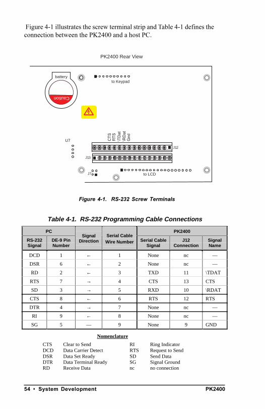
Figure 4-1 illustrates the screw terminal strip and Table 4-1 defines theconnection between the PK2400 and a host PC.
Figure 4-1. RS-232 Screw Terminals
U7
to Keypad
PK2400 Rear View
Caution
J12
J13
to LCDJ7
battery
RT
SC
TS
\RD
at\T
Dat
Gnd
Table 4-1. RS-232 Programming Cable Connections
PC PK2400
RS-232Signal
DE-9 PinNumber
SignalDirection
Serial CableWire Number Serial Cable
SignalJ12
ConnectionSignalName
DCD 1 ← 1 None nc —
DSR 6 ← 2 None nc —
RD 2 ← 3 TXD 11 \TDAT
RTS 7 → 4 CTS 13 CTS
SD 3 → 5 RXD 10 \RDAT
CTS 8 ← 6 RTS 12 RTS
DTR 4 → 7 None nc —
RI 9 ← 8 None nc —
SG 5 — 9 None 9 GND
Nomenclature
CTS Clear to SendDCD Data Carrier DetectDSR Data Set ReadyDTR Data Terminal ReadyRD Receive Data
RI Ring IndicatorRTS Request to SendSD Send DataSG Signal Groundnc no connection
PK2400 System Development s 55
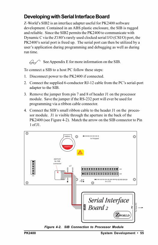
Developing with Serial Interface BoardZ-Worlds SIB2 is an interface adapter useful for PK2400 softwaredevelopment. Contained in an ABS plastic enclosure, the SIB is ruggedand reliable. Since the SIB2 permits the PK2400 to communicate withDynamic C via the Z180s rarely used clocked serial I/O (CSI/O) port, thePK2400s serial port is freed up. The serial port can then be utilized by ausers application during programming and debugging as well as duringrun time.
See Appendix E for more information on the SIB.
To connect a SIB to a host PC follow these steps:
1. Disconnect power to the PK2400 if connected.
2. Connect the supplied 6-conductor RJ-12 cable from the PCs serial-portadapter to the SIB.
3. Remove the jumper from pin 7 and 8 of header J1 on the processormodule. Save the jumper if the RS-232 port will ever be used forprogramming via a ribbon cable connector.
4. Connect the SIBs small ribbon cable to the header J1 on the proces-sor module. J1 is visible through the aperture in the back of thePK2400 (see Figure 4-2). Match the arrow on the SIB connector to Pin1 of J1.
Figure 4-2. SIB Connection to Processor Module
$
U7
to Keypad
Caution
J11
J12
J13
to LCD
battery
aperturefor SIB
connector
J7
To H
ost P
C

PK240056 s System Development
5. Verify that the baud rate of the host PCs is set at 9600, 19200, or 57600.
6. Reconnect the power supply to the PK2400. A minimum 9 V directcurrent must be connected to the PK2400.
The system is now ready for programming in SIB2 programming mode.
Running a Program StandaloneUse the following steps to run a program standalone (not under DynamicC control):
1. Download compiled program to flash EPROM.
2. Power down the PK2400.
3. Remove either the SIB2 or the jumper from pins 1 and 2 of J1, depend-ing upon which programming mode was used.
4. Reapply power. The PK2400 begins executing a program automatically.
Returning To Programming ModeUse the following steps to return to programming mode:
1. Remove power.
2. Reinstall the jumper connecting pins 1 and 2 of J1, or reconnect theSIB2. See Figure 4-2.
3. Reapply power.
PK2400 System Development s 57
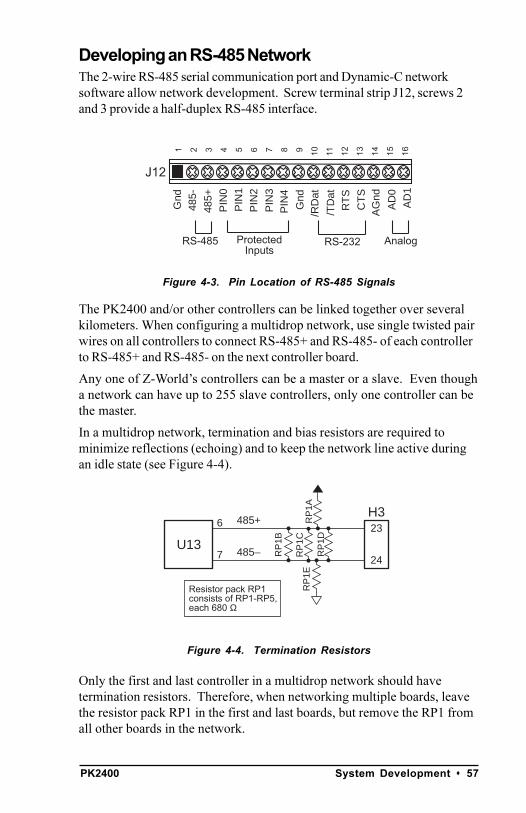
Developing an RS-485 NetworkThe 2-wire RS-485 serial communication port and Dynamic-C networksoftware allow network development. Screw terminal strip J12, screws 2and 3 provide a half-duplex RS-485 interface.
Figure 4-3. Pin Location of RS-485 Signals
The PK2400 and/or other controllers can be linked together over severalkilometers. When configuring a multidrop network, use single twisted pairwires on all controllers to connect RS-485+ and RS-485- of each controllerto RS-485+ and RS-485- on the next controller board.
Any one of Z-Worlds controllers can be a master or a slave. Even thougha network can have up to 255 slave controllers, only one controller can bethe master.
In a multidrop network, termination and bias resistors are required tominimize reflections (echoing) and to keep the network line active duringan idle state (see Figure 4-4).
Figure 4-4. Termination Resistors
Only the first and last controller in a multidrop network should havetermination resistors. Therefore, when networking multiple boards, leavethe resistor pack RP1 in the first and last boards, but remove the RP1 fromall other boards in the network.
23
24
H3
U13
485+
485–
6
7
RP
1ER
P1A
RP
1B
RP
1C
Resistor pack RP1consists of RP1-RP5,each 680 Ω
RP
1D
J12
16151413121110987654321
ProtectedInputs
RS-485
AG
nd
/RD
at
/TD
atR
TS
CT
S
Gnd
AD
0A
D1
PIN
2P
IN1
PIN
048
5+
Gnd
PIN
4P
IN3
485-
RS-232 Analog

PK240058 s System Development
Follow these steps to access and remove the terminator resistors on theprocessor module:
1. Remove screws from the standoffs that connect the front panel to theback plate.
2. Unfold the rear processor assembly. Do not disconnect the keypadribbon cable from the rear processor assembly.
3. Remove resistor pack.
Figure 4-5 illustrates an unfolded PK2400 with the resistor pack exposed.
Figure 4-5. Processor Module Resistor Pack RP1 Location
Y1
U6
U1
PIO
1
U2
Y2
H3
JP1
Z180
U3
JP2
PIO
2
U9
U7
U8
H1
H2
J1
EP
RO
M
RP
1
U4
Programming Port, toSerial Interface Board
(1.18, 0.94)
(3.24, 0.66)
(6.20, 1.39)
keypad ribbon cable
J4
J2
J5
J3
J8J9
J7 J6
J1
J11,underside
J12, undersideJ13, underside
Thermistor
to keypad
to LCD
aperturefor SIB
connector
to LCD
to Processor
to Processor
battery
Resistor Pack
J10

PK2400 Software Reference s 59
CHAPTER 5: SOFTWARE REFERENCE
The functions described in this chapter operate the PK2400 input andoutput interfaces. Most functions are in the EZIOPK24.LIB library Othersoftware functions are in the Dynamic C BIOS of the PK2400s onboardflash EPROM.

PK240060 s Software Reference
Software Development OptionsApplications can be developed on the PK2400 series by using either theRS-232 port or the Serial Interface Board (SIB) port. However, since theSIB port is a dedicated programming port, using it for programming leavesthe RS-232 port free for the embedded application.
See Chapter 4 and Appendix E for information onprogramming with the SIB.
Dynamic C Development SoftwareThe PK2400 is programmed with Z-Worlds Dynamic C, an integrateddevelopment environment that runs under Windows 3.x, 95, and NT.Dynamic C includes an editor, compiler, downloader, and debugger.Dynamic C is available in the following two versions:
Standard: Maximum 80K of code
This version of Dynamic C is suitable for programs up to 80K withlimited access to extended memory. (Data items can not bedeclared in extended memory.)
Deluxe: Maximum 512K of code, 512K of data
This version supports programs (up to 512K code and 512K data)with full access to extended memory.
Dynamic C ManualsZ-World offers three Dynamic C manuals for programming reference:
Dynamic C Technical Reference Dynamic C Application Frameworks Dynamic C Function Reference
Supplied SoftwareSoftware drivers for controlling the PK2400s I/O are provided withDynamic C 5. In order to use the supplied routines defined is this chapter,use the EZIOPK24.LIB Dynamic C library. An application program canutilize the library by including the following line at the top of the program:
#use eziopk24.lib
Some functions are located in other libraries and these exceptions arenoted in the following individual entries:
EZIOCMMN.LIB
I /O functions that are not specific to the PK2400 series controllers.This library is automatically used by EZIOPK24.LIB.
$

PK2400 Software Reference s 61
KP.LIB
Keypad-related functions. The application should explicitly #use thislibrary if the keypad is used.
GLCD.LIB
Graphic LCD related functions. The application should explicitly #usethis library if the graphic LCD is used.
KDI.LIB
Keypad/display interface-related functions. This library is automati-cally used by GLCD.LIB and KDI.LIB. Note that backlight, buzzer,and contrast control are all implemented in this library.
Functions that are not controller specific are not discussed in this manual.Refer to the Dynamic C manuals for information about functions such asserial communication, string, and math functions.
Memory
Flash EPROM Functions int WriteFlash(unsigned long physical_addr,
char *buf, int count )
Writes count number of bytes pointed to by buf to the flash EPROMabsolute data location physical_addr. Allocates data location bydeclaring the byte arrays as initialized arrays or declares initialize xdataarray. If byte array is declared, converts logical memory to physicalmemory with phy_adr(array). For initialized xdata, the array namecan be passed directly.
PARAMETER1: Flash EPROM absolute data location
PARAMETER2: Pointer to bytes to write
PARAMETER3: Number of bytes to write
RETURN VALUE: 0 if WriteFlash is successful
-1 if flash EPROM is not used
-2 if physical_address is inside BIOS area
-3 if physical_address is within Symbol Area orthe simulated EEPROM area
-4 if write time-out to the flash EPROM
LIBRARY: DRIVERS.LIB

PK240062 s Software Reference
Nonvolatile StorageThe top 512 bytes of PK2400s flash EPROM are reserved as nonvolatilememory. This area can be used to store important system state informa-tion such as A/D conversion constants in order for the PK2400 to recoverfrom power outages.
To ensure compatibility with Z-Worlds product line, the nonvolatilestorage area simulates the EEPROM that certain Z-World controllers usefor nonvolatile storage. The high level Dynamic C functions are exactlythe same for all versions of all Z-Worlds controllers. These driversautomatically take care of all low-level differences between physicalmemory devices.
The logical addresses of the simulated EEPROM are 0 to 511.
Dynamic C BIOS reserves flash EPROM location 0 to store operationmode and location 1 to store the baud code. The remainder of thelocations are available for use.
int ee_rd ( int address )
Reads and returns data from flash EPROM storage location address.
The function returns 1 if a non-flash EPROM is used.
int ee_wr ( int address, char data )
Writes data to simulated-EEPROM storage location address.
The function returns 1 if a non-flash EPROM is used.
int WriteFlash (unsigned longaddr, char* buf, intnum )
Writes num bytes from buf to flash EPROM, starting at addr.
The term addr is an absolute physical address.
To do this, allocate flash EPROM data in the Dynamic C program bydeclaring initialized variables or arrays, or initialized xdata. Forxdata, the data name must pass directly to this function:
xdata my_data 0, 0xFF, 0x08 ;...
WriteFlash( my_data, my_buffer, my_count );
For normal data, the physical address of the data must pass to thisfunction:
char xxx[] = 0, 0xFF, 0x08 ;...
WriteFlash( phy_adr(xxx), my_buffer,my_count );

PK2400 Software Reference s 63
The function returns
0 if the operation was successful1 if no flash EPROM is present2 if a physical address is within the BIOS area (low 8K)3 if a physical address is within the symbol table4 if the write times out
In order for this function to work, some form of initialization has to beincluded when declaring the data. If the data is not declared, it will beplaced in RAM instead of ROM and this function will not work.Writing to read-only memory may seem contradictory, but flashEPROM, despite its name, is not really read-only memory. Writing toflash EPROM, in essence, treats the flash memory as read/writenonvolatile memory.
Flash EPROM manufacturers rate their devices conservativelyat 10,000 writes. In tests, a flash EPROM can last for 100,000writes. When this limit is reached, the system will fail and theintegrated circuit must be replaced.
Digital Input and Output
Digital Input/Output FunctionsThe digital I/O functions provide easy software access to the PK2400sprotected inputs, high-current outputs, and relay outputs. The state ofthe latching relays is determined by the number of on-off cycles for therelay. Each time the relay is deenergized or reenergized, it changes states.Latching relays maintain their state even when power is removed from thePK2400. When using latching relays, make sure that any equipmentconnected to the latching relays will continue to operate safely or shutdown in the event of a controller malfunction or power loss.
When using nonlatching relays, the state is determined by thestate of the corresponding output. If the output is on, therelay is in the energized state. If the output is off, the relay isin the deenergized state.
void eioBrdInit( int flags )
Initializes the PK2400 board. The application should call this functionbefore performing any I/O operations, including digital input, digitaloutput, analog input, graphic LCD, or keypad operations.
PARAMETER: flags should be zero.
RETURN VALUE: N/A.
LIBRARY: EZIOCMMN.LIB
!
!

PK240064 s Software Reference
int eioBrdDI( unsigned chanNum )
Reads the state of an input channel.
PARAMETER: chanNum must be a number ranging from 0 (for PIN-0)through 8 (for PIN-8) inclusively.
RETURN VALUE: returns 0 if and only if the input channel reads low;returns 1 if and only if the input channel reads high; sets the flagEIO_NODEV in eioErrorCode and returns -1 if and only if the channeldoes not exist (i.e., if chanNum is greater than 8).
LIBRARY: EZIOPK24.LIB
Table 5-1 lists software input channel assignments.
If digital input PIN-0 (input channel 0) is grounded, the digital outputOUT-0 (output channel 0) is disabled OFF. Otherwise, the digital outputis enabled.
Program 5-1. Reflect Input State to Output
Table 5-1. Software InputChannel Assignments
Label Channel Assignment
PIN-0 0
PIN-1 1
PIN-2 2
PIN-3 3
PIN-4 4
PIN-5 5
PIN-6 6
PIN-7 7
PIN-8 8
#use ezio.lib // general I/O definitions#use eziopk24.lib // pk2400 specific defns#define IN_CHAN 0 // define input channel#define OUT_CHAN 0 // define output channelmain() eioBrdInit(0); while (1) // do this indefinitely eioBrdDO(OUT_CHAN,eioBrdDI(IN_CHAN)); hitwd(); // hit watchdog

PK2400 Software Reference s 65
int eioBrdDO( unsigned chanNum, char state )
Changes the state of an output channel.
PARAMETER 1: chanNum must range from 0 (for OUT-0) through 7(for OUT-7) inclusively. OUT-4 and OUT-5 will also controlnonlatching relays 1 and 2. OUT-6 and OUT-7 will also controllatching relays 1 and 2.
PARAMETER 2: state is 0 if and only if the corresponding output isto be disabled OFF or 1 if and only if the corresponding output is tobe enabled ON.
RETURN VALUE: returns 0 if and only if chanNum is within range;sets the flag EIO_NODEV in eioErrorCode and returns -1 if and onlyif chanNum is out of range.
LIBRARY: EZIOPK24.LIB
Table 5-2 lists software output channel assignments.
Refer to the Dynamic C subdirectory SAMPLES\PK24XX foradditional sample programs.$
Table 5-2. Software Output Channel Assignments
Label Channel Assignment
Out-0 0
Out-1 1
Out-2 2
Out-3 3
Out-4 4
Out-5 5
Out-6 6
Out-7 7

PK240066 s Software Reference
Advanced Input/Output ProgrammingMost I/O devices on the PK2400 series controllers, including digital input,digital output, analog input, 485 driver, keypad, and graphic LCD arecontrolled through the two Zilog PIO chips (Z84C20) on the PK2400sprocessor module. Z-World recommends that the application programmeruse the supplied functions documented in this chapter for a simpleinterface to the hardware.
However, if necessary, the application programmer may write custom low-level driver routines for size, speed, or both. In order to write the low-levelroutines that interact with the controller hardware, the following items arenecessary:
PK2400 Schematics
BL1500 Schematics (processor module of the PK2400)
Specifications of the control chip(s). Probably including the specifica-tions of the PIO (Z84C20) chip from Zilog
The low-level driver programmer also needs to know how the PIO chipsare mapped in the Z180 I/O space. The following list describes how thePIO chips are interfaced to the Z180 processor.
U2 (PIO No. 1) Port A uses vector 0x12 in the interrupt table
Port B uses vector 0x14 in the interrupt table
Port A data register is at 0xc0 in the I/O space
Port A control register is at 0xc2 in the I/O space
Port B data register is at 0xc1 in the I/O space
Port B control register is at 0xc3 in the I/O space
U9 (PIO No. 2) Port A uses vector 0x22 in the interrupt table
Port B uses vector 0x24 in the interrupt table
Port A data register is at 0x80 in the I/O space
Port A control register is at 0x82 in the I/O space
Port B data register is at 0x81 in the I/O space
Port B control register is at 0x83 in the I/O space

PK2400 Software Reference s 67
Serial Communication FunctionsThere are several libraries that can be used for serial communication.Serial communication functions, constants, and definitions are describedin the Dynamic C Function Reference Manual and Dynamic C Applica-tion Framework Manual. AASC.LIB is the recommended serial commu-nication library.
RS-485 Functions void on_485( void )
Turns the RS-485 transmitter on.
PARAMETER: none
RETURN VALUE: none
LIBRARY: DRIVERS.LIB
void off_485(void)
Turns the RS-485 transmitter off.
PARAMETER: none
RETURN VALUE: none
LIBRARY: DRIVERS.LIB

PK240068 s Software Reference
Analog-to-Digital Converter Drivers void eioBrdInit( int flags )
Initializes the PK2400 board. The application program should call thisfunction before performing any I/O operations, including digital input,digital output, analog input, graphic LCD, or keypad operations.
PARAMETER: flags should be zero
RETURN VALUE: N/A
LIBRARY: EZIOCMMN.LIB
int _eioBrdAI(unsigned int eioAddr )
Reads an input and performs analog-to-digital conversion. Does notcheck validity of the parameter and does not convert according tocalibration coefficients (see eioBrdAI).
PARAMETER: eioAddr specifies an input number of 0, up to 15.eioAddr values 0 to 1 represent analog inputs AD0 and AD1 and willcause the function to return the 12-bit A/D value read on an input. IfeioAddr is between 11 and 15, the function returns the A/D valuesof internal channels of the ADC chip.
RETURN VALUE: A 12-bit unsigned
LIBRARY: EZIOPK24.LIB
float eioBrdAI(unsigned int eioAddr )
Reads an input and performs analog-to-digital conversion. SetseioErrorCode if eioAddr is out of range.
PARAMETER: eioAddr specifies an input number of 0 to 1 or 16 to17 to be read. eioAddr values 0 and 1 represent analog inputs AD0and AD1 and will cause the function to return the voltage read on aninput. eioAddr values 16 and 17 also represent analog inputs AD0and AD1, but cause the function to return a 12-bit raw data value forthe analog input.
RETURN VALUE: For eioAddr values 0 and 1, if the read is success-ful, the function will return the voltage read. For eioAddr values 16and 17, if the read is successful, the function returns the 12-bit rawdata value read from the A/D converter.
LIBRARY: EZIOCMMN.LIB

PK2400 Software Reference s 69
· int eioBrdACalib( int eioAddr,unsigned int d1,unsigned int d2, float v1, float v2 )
Calculates the calibration constants for an analog input channel usingtwo known voltages and two corresponding raw data readings. Storesthe calibration constants in EEPROM.
PARAMETER 1: eioAddr is the analog input channel
PARAMETER 2: d1 is the raw data corresponding to v1
PARAMETER 3: d2 is the raw data corresponding to v2
PARAMETER 4: v1 is the known voltage used to obtain d1
PARAMETER 5: v2 is the known voltage used to obtain d2
RETURN VALUE: 0 if successful, -1 if eioAddr is out of range.
LIBRARY: EZIOCMMN.LIB
Since the PK2400 is calibrated at the factory, use the abovefunction only if it is necessary to recalibrate the PK2400.
Using the Liquid Crystal Display and KeypadThe following functions provide routines that write to the LCD, and readfrom the keypad. Include the following directives:
#use wintek.lib#use kp.lib#use glcd.lib
These directives provide information to the compiler about the graphicLCD and keypad.
void eioBrdInit( int flags )
Initializes the PK2400 board. The application program should call thisfunction before performing any I/O operations, including digital input,digital output, analog input, graphic LCD, or keypad operations.
PARAMETER: flags should be zero.
RETURN VALUE: N/A
void glSetBrushType( int type )
Sets the brush type for all following graphics operations in this library.Controls how pixels are drawn on the screen with respect to existing pixels.
PARAMETER1: This is the type of the brush. Possible values areGL_SET for forcing pixels on, GL_CLEAR for forcing pixels off,GL_XOR for toggling the existing pixels and GL_BLOCK to overwritethe entire memory location corresponding to the pixel.
RETURN VALUE: None
!

PK240070 s Software Reference
int glInit()
Initializes the LCD module (software and hardware). This functionshould be called after calling eioBrdInit. Call this function beforeperforming any LCD operations.
RETURN VALUE: Returns the status of the LCD. If the initializationwas successful, this function returns 0. Otherwise, the returned valueindicates the LCD status.
int glBlankScreen()
Blanks the screen of the LCD.
RETURN VALUE: The returned value indicates the status of the LCDafter the operation.
int glPlotDot( int x, int y )
Plots one pixel on the screen at coordinate (x,y).
PARAMETER1: the x-coordinate of the pixel to be drawn
PARAMETER2: the y-coordinate of the pixel to be drawn
RETURN VALUE: Status of the LCD after the operation
void glPlotLine( int x1, int y1, int x2, int y2 )
Plots a line on the LCD.
PARAMETER1: x-coordinate of first end-point
PARAMETER2: y-coordinate of first end-point
PARAMETER3: x-coordinate of second end-point
PARAMETER4: y-coordinate of second end-point
RETURN VALUE: None
void glPutBitmap( int x, int y, int bmWidth,int bmHeight,char *bm )
Displays a bitmap stored in root memory on the LCD. For bitmapsdefined in xmem memory, use glXPutBitmap.
PARAMETER1: x-coordinate of the bitmap (left edge)
PARAMETER2: y-coordinate of the bitmap (top edge)
PARAMETER3: width of the bitmap
PARAMETER4: height of the bitmap
PARAMETER5: pointer to the bitmap
RETURN VALUE: None

PK2400 Software Reference s 71
void glXPutBitmap( int x, int y, int bmWidth,int bmHeight,unsigned long bmPtr )
Displays a bitmap stored in xmem on the LCD. For bitmaps stored inroot memory, use glPutBitmap.
PARAMETER1: x-coordinate of the bitmap (left edge)
PARAMETER2: y-coordinate of the bitmap (top edge)
PARAMETER3: width of the bitmap
PARAMETER4: height of the bitmap
PARAMETER5: pointer to the bitmap
RETURN VALUE: None
void glGetBitmap( int x, int y, int bmWidth,int bmHeight,char *bm )
Gets a bitmap from the LCD.
PARAMETER1: x-coordinate of the bitmap (left edge)
PARAMETER2: y-coordinate of the bitmap (top edge)
PARAMETER3: width of the bitmap
PARAMETER4: height of the bitmap
PARAMETER5: pointer to the bitmap
RETURN VALUE: None
void glFontInit( struct _fontInfo *pInfo,char pixWidth, char pixHeight, unsignedstartChar, unsigned endChar,char bitmapBuffer )
Initializes a font descriptor with the bitmap defined in the root memory.For fonts with bitmaps defined in xmem, use glXFontInit.
PARAMETER1: pointer to the font descriptor to be initialized
PARAMETER2: width of each font item (must be uniform for all items)
PARAMETER3: height of each font item (must be uniform for all items)
PARAMETER4: offset to the first usable item (useful for fonts forASCII or other fonts with an offset)
PARAMETER5: index of the last usable font item
PARAMETER6: pointer to a linear array of font bitmap
RETURN VALUE: None

PK240072 s Software Reference
void glXFontInit( struct _fontInfo *pInfo,char pixWidth, char pixHeight, unsignedstartChar, unsigned endChar, ulong xmemBuffer )
Initializes a font descriptor that has the bitmap defined in xmem. Forbitmaps defined in root memory, use glFontInit.
PARAMETER1: pointer to the font descriptor to be initialized
PARAMETER2: width of each font item (must be uniform for all items)
PARAMETER3: height of each font item (must be uniform for all items)
PARAMETER4: offset to the first usable item (useful for fonts forASCII or other fonts with an offset)
PARAMETER5: index of the last usable font item
PARAMETER6: pointer to a linear array of font bitmap
RETURN VALUE: None
void glPutFont( int x, int y, struct fontInfo*pInfo, unsigned code )
Puts an entry from the font table to the LCD.
PARAMETER1: x-coordinate of the entry (left edge)
PARAMETER2: y-coordinate of the entry (top edge)
PARAMETER3: pointer to the font descriptor that describes the fonttable to be indexed
PARAMETER4: code (offset) in the font table that indexes the bitmapto display
RETURN VALUE: None
void glVPrintf( int x, int y, struct fontInfo*pInfo, char *fmt, void *firstArg )
Prints a formatted string on the LCD screen, similar to vprintf.
PARAMETER1: x-coordinate of the text (left edge)
PARAMETER2: y-coordinate of the text (top edge)
PARAMETER3: pointer to font descriptor that describes the font usedfor printing the text
PARAMETER4: pointer to the string that describes the format
PARAMETER5: pointer to the first argument
RETURN VALUE: None

PK2400 Software Reference s 73
void glPrintf( int x, int y, struct _fontInfo*pInfo, char *fmt,... )
Prints a formatted string (much like printf) on the LCD screen
PARAMETER1: x-coordinate of the text (left edge)
PARAMETER2: y-coordinate of the text (top edge)
PARAMETER3: pointer to the font descriptor used for printing on theLCD screen
PARAMETER4: pointer to the format string
RETURN VALUE: None
void glPlotCircle( int xc, int yc, int rad )
Draws a circle on the LCD.
PARAMETER1: x-coordinate of the center
PARAMETER2: y-coordinate of the center
PARAMETER3: radius of the circle
RETURN VALUE: None
int wtDisplaySw( int onOff )
Switches the display on and off.
PARAMETER1: If this parameter is 1, the display is turned on. If thisparameter is 0, the display is turned off.
RETURN VALUE: Status of the LCD after the operation
void kdiELSw( int value )
Switches the EL backlight of the LCD.
PARAMETER1: 1 to turn the backlight on, 0 to turn the backlight off
RETURN VALUE: None
void kdiBuzSw( int value )
Switches the buzzer on the keypad display interface board.
PARAMETER1: 1 to turn the buzzer on, 0 to turn the buzzer off
RETURN VALUE: None
void kdiSetContrast( unsigned content )
Sets the contrast control to content.
PARAMETER1: Specifies the contrast (the higher the value, the higherthe contrast)
RETURN VALUE: None

PK240074 s Software Reference
void kpInit( int (*changeFn)() )
Initializes the kp module. This function should be called before otherfunctions of this module are called. If the default keypad scanningroutine will be used, use kpDefInit instead of this function.
PARAMETER1: This is a pointer to a function which will be calledwhen the driver detects a change (when kpScanState is called).Two arguments are passed to the call-back function. The first argu-ment is a pointer to an array that indicates the current state of thekeypad. The second is a pointer to an array that indicates whatkeypad positions are changed and detected by kpScanState. Thebyte offset in the array represents the line pulled high (row number),and the bits in a byte represents the positions (column number) readback.
RETURN VALUE: None.
int kpScanState()
Scans the keypad and detect any changes to the keypad status. Itreturns non-zero if there is any change. If kpInit is called with anon-NULL function pointer, that function will be called with the stateof the keypad. This function should be called periodically to scan forkeypad activities.
RETURN VALUE: 0 if there is no change to the keypad, non-zero ifthere is any change to the keypad.
int kpDefStChgFn( char *curState, char *changed )
This is the default state change function for the default get keyfunction kpDefGetKey. This function is called back bykpScanState when there is a change in the keypad state. If thecurrent key is not read by kpDefGetKey, the new key pressed willnot be registered.
PARAMETER1: Points to an array that reflects the current state of thekeypad (bitmapped, 1 indicates key is not currently pressed).
PARAMETER2: Points to an array that reflects the CHANGE ofkeypad state from the previous scan. (bitmapped, 1 indicates there wasa change).
RETURN VALUE: -1 if no key is pressed. Otherwise it returns thenormalized key number. The normalized key number is8*row+col+edge*256.edge is 1 if the key is released, and 0 ifthe key is pressed.

PK2400 Software Reference s 75
int kpDefGetKey()
This is the default get key function. It returns the key previouslypressed (i.e., from the one-keypress buffer). The key pressed isactually interpreted by kpDefStChgFn, which is called back bykpScanState. kpDefInit should be used to initialize themodule.
RETURN VALUE: -1 if no key is pressed. Otherwise, it returns thenormalized key number. The normalized key number is8*row+col+edge*256.edge is 1 if the key is released, and 0 ifthe key is pressed.
void kpDefInit()
Initializes the module to use the default state change function tointerpret key presses when kpScanState is called. UsekpDefGetKey to get the code of the last key pressed.
RETURN VALUE: N/A

PK240076 s Software Reference
Real-Time Clock Integrated CircuitThe RTC IC has the following features:
A clock/calendar that accounts for leap years and the varyingnumber of days in a month
A 31-byte scratchpad RAM
An application program can write to both the clock/calendar and the RAMin burst mode. In this mode, the software specifies a start location andthen writes multiple, consecutive characters to the RTC integrated circuit.The integrated circuit automatically increments the internal address for thenext write. This approach is more efficient than setting the address foreach byte in the non-burst mode.
Global Time and Date StructureDynamic C automatically creates the global structure shown in Program5-2 to hold the time and date.
Program 5-2. Global Time and Date Structure
Since Dynamic C automatically creates this structure, it should not bedeclared in an application program.
int tm_rd ( struct tm *t )
Stores the real-time clock (RTC) ICs current contents into the struc-ture *t.
If the RTC is halted, this function stores the value for midnight, 1January 1980 in *t, and returns 1. Otherwise, the function stores thecurrent time in *t and returns 0.
int tm_wr ( struct tm *t )
Writes the values in the structure *t to the RTC.
The function returns 0 if successful, or 1 if it is unable to start theRTC.
struct tm char tm_sec; // 0-59 char tm_min; // 0-59 char tm_hour; // 0-23 char tm_mday; // 1-31 char tm_mon; // 1-12 char tm_year; // 0-150 (1900-2050) char tm_wday; // 0-6 where 0 means Sunday;

PK2400 Software Reference s 77
int WriteRam1302 ( int ram_loc, byte data )
Writes data to any of the 31 (030) RAM locations of the DS1302.
The function returns 1 if successful and 1 if ram_loc is out of range.
int ReadRam1302 ( int ram_loc )
Reads data from any of the 31 (030) RAM locations of the DS1302.
The result of the function is the data value or 1 if ram_loc is out ofrange.
void WriteBurst1302 ( void* pdata, int count )
Writes count bytes, in burst mode, to the DS1302, starting at RAMlocation 0.
The parameter pdata points to the data.
void ReadBurst1302 ( void* pdata, int count )
Reads count bytes, in burst mode, from the DS1302, starting at RAMlocation 0.
The parameter pdata points to a storage area for the data.
void Write1302 ( int reg, byte data )
Writes data to a specified register of the DS1302.
int Read1302 (int reg)
Reads data from a specified register of the DS1302.
The result of the function is the data value.

PK240078 s Software Reference
Sample ProgramsTable 5-3 lists and describes sample programs in the subdirectorySAMPLES\PK24XX in the Dynamic C directory.
Additional SoftwareFor Watchdog information, refer to descriptions of the function hitwd inthe Dynamic C manuals.
For reading and writing Simulated EEPROM data, refer to descriptions ofthe functions ee_rd and ee_wr in the Dynamic C manuals.
For Power Fail Flag information, refer to the descriptions of the function_sysIsPwrFail and sysIsPwrFail in the Dynamic C manuals.
For Resetting the Board information, refer to descriptions of the functionssysForceSupRst, sysIsSuperReset, _sysIsSuperReset,sysForceReset, _sysIsWDTO, and sysIsWDTO in the Dynamic Cmanuals.
Table 5-3. Sample Programs in SAMPLES\PK2400XX
Program Description
DEMO.C Dynamic C Deluxe version only. A program todemonstrate graphic LCD and keypad features.
KPDEFLT.C A program to demonstrate how to use thedefault keypad scanning routine.
SHOWIN.C Displays the current state and history of alldigital input lines on the graphic LCD aswaveforms.
LCHRELAY.C Demonstrates how to use the latching relays.
FANCY1.C Dynamic C Deluxe version only. Uses theLCD and keypad to reflect the states of thedigital input lines and to toggle the digitaloutput lines.

PK2400 Troubleshooting s 79
APPENDIX A: TROUBLESHOOTING
Appendix A provides procedures for troubleshooting system hardwareand software.

PK240080 s Troubleshooting
Out of the BoxCheck the items mentioned in this section before starting development.
Verify that the PK2400 runs in standalone mode before connecting anyexpansion boards or I/O devices.
Verify that the entire host system has good, low-impedance, separategrounds for analog and digital signals. Often the PK2400 is connectedbetween the host PC and another device. Any differences in groundpotential from unit to unit can cause serious problems that are hard todiagnose.
Do not connect analog ground to digital ground anywhere.
Double-check the connecting ribbon cables to ensure that all wires goto the correct screw terminals on the PK2400.
Verify that the host PCs COM port works by connecting a known tobe good serial device to the COM port. Remember that COM1/COM3and COM2/COM4 share interrupts on a PC. User shells and mousedrivers, in particular, often interfere with proper COM port operation.For example, a mouse running on COM1 can preclude running Dy-namic C on COM3.
Use the supplied Z-World power supply. If another power supplymust be used, verify that it has enough capacity and filtering tosupport the PK2400.
Use the Z-World cables supplied. The most common fault of user-made cables is failure to properly assert CTS at the RS-232 port of thePK2400. Without CTSs being asserted, the PK2400s RS-232 port willnot transmit. Assert CTS by either connecting the RTS signal of thePCs COM port or looping back the PK2400s RTS.
Experiment with each peripheral device connected to the PK2400 todetermine how it appears to the PK2400 when powered up, powereddown, and/or when its connecting wiring is open or shorted.

PK2400 Troubleshooting s 81
Dynamic C Will Not StartIn most situations, when Dynamic C will not start an error messageannouncing a communication failure will be displayed. Following is a listof situations causing an error message and possible resolutions.
Wrong Baud Rate In rare cases, the baud rate has to be changedwhen using the Serial Interface Board for development.
Wrong Communication Mode Both sides must be talking RS-232.
Wrong COM Port A PC generally has two serial ports: COM1 andCOM2. Specify the port being used in the Dynamic C Target Setupmenu. Use trial and error, if necessary.
Wrong Operating Mode Communication with Dynamic C will be lostif the PK2400s jumper is set for standalone operation. Reconfigurethe board for programming mode.
Wrong Memory Size Jumpers JP1 and JP2 of the PK2400 specify theEPROM size.
If all else fails, connect the serial cable to the PK2400 after power up. Ifthe PCs RS-232 port supplies a large current (most commonly on portableand industrial PCs), some RS-232 level converter ICs go into a nonde-structive latch-up. Connect the RS-232 cable after power up to eliminatethis problem.
Dynamic C Loses Serial LinkIf the program disables interrupts for a period greater than 50 ms,Dynamic C will lose its serial link with your program. Make sure thatinterrupts are not disabled for a period greater than 50 ms.
PK2400 Repeatedly ResetsThe PK2400 resets every 1.0 seconds if the watchdog timer is not hit. Ifa program does not hit the watchdog timer, then the program will havetrouble running in standalone mode. To hit the watchdog, make a call tothe Dynamic C library function hitwd.

PK240082 s Troubleshooting
Common Programming Errors Values for constants or variables out of range. Table A-1 lists and
defines ranges for variables and constants.
Mismatched types. For example, the literal constant 3293 is of typeint (16-bit integer). However, the literal constant 3293.0 is of typefloat. Although Dynamic C can handle some type mismatches,avoiding them is the best practice.
Counting up from, or down to, one instead of zero. In software,ordinal series often begin or terminate with zero, not one.
Confusing a functions definition with an instance of its use in alisting.
Not ending statements with semicolons.
Not inserting commas as required in functions parameter lists.
Leaving out an ASCII space character between characters forming adifferent legal, but unwanted operator.
Confusing similar looking operators such as && with &,== with =, or // with /.
Table A-1. Constant and Variable Ranges
Type Range
int –32,768 (–215) to+32,767 (215–1)
long int −2,147,483,648 (−231) to+2147483647 (231 −1)
float 1.18 × 10–38 to3.40 × 1038
char 0 to 255

PK2400 Specifications s 83
APPENDIX B: SPECIFICATIONS
Appendix B presents the dimensions and specifications for the PK2400controller and its components.

PK240084 s Specifications
SpecificationsTable B-1 lists the electrical, mechanical, and environmental specificationsfor the PK2400.
Table B-1. General Specifications
Parameter Specification
Product Size 7.75″ × 4.0″ × 1.125″ (197 mm × 102 mm × 28mm)
Enclosure Size 7.85″ × 4.1″ × 1.5″ (200 mm × 104 mm × 38 mm)
Bezel Size 8.5″ × 4.75″ × 0.125″ (216 mm × 121 mm × 3.2mm)
OperatingTemperature
0°C to +50°C
Humidity 5% to 95%, noncondensing
Input Voltage, Current 9 V to 12 V DC, 150 mA plus 30 mA per activerelay
Configurable I/O Digital inputs can be pulled up or down
Digital Inputs 9 protected, –20 V to +24 V
Digital Outputs6 channels, sourcing (2985). Sinking drivers(2803) optional.
Relays2 nonlatching relays rated 2 A at 30 V DC or 0.5A at 120 V AC
Analog Inputs2, conditioned, 12-bit (two other A/D channelsinternally support the temperature sensor)
Analog outputs None
ResistanceMeasurement Input
None
Processor Z180
Clock 9.216 MHz
SRAM 128K, socketed; 256K optional
EPROM None
Flash 128K, socketed
EEPROM None
Counters Software-implementable
continued…

PK2400 Specifications s 85
For CE compliance, the maximum relay switching voltage isless than 50 V AC or 75 V DC.
Table B-1. General Specifications (concluded)
Parameter Specification
Serial Ports One RS-232 (with RTS/CTS handshake)One RS-485 (two-wire)
Serial Rate Up to 57,600 bps
Watchdog/Supervisor Yes
Time/Date Clock Yes
Backup Battery Yes, 3 V lithium coin-type, 560 mA⋅h
Keypad and LCD Yes
Expansion Port None
!

PK240086 s Specifications
7.75(197)
0.93(23.6)
0.2 typ(5)
1.485 (37.7)
0.2
typ
(5)
1.258 (32.0)
0.1 (2.5)
0.15 dia, 4x(3.8)
4.002(101.7) 4.825
(122.6)
0.75
(19)
4.0
(102
)
~1.
025
(26)
2.749(69.8)
Hardware DimensionsThe PK2400 measures 7.75²W × 4.0²L × 1.125²H.
The keys in the 4 × 5 matrix are 0.4″ square. The simulated bezels are 0.5²square. The keys are spaced 0.525″ apart in each direction. The radius onthe key aperture is 0.0625″ (1/16″).
The keys in the 1 × 3 array are 0.4″ × 0.5″. The simulated bezels are0.5″ × 0.6″. The keys are spaced 0.525″ apart vertically. The radius on thekey aperture is 0.0625″ (1/16″).
The mounting holes are 0.15″ in diameter.
Figure B-1 illustrates the PK2400s dimensions and mounting holelocations.
Figure B-1. PK2400 Dimensions and Mounting Hole Locations

PK2400 Specifications s 87
Figure B-2 illustrates the optional mounting bezel dimensions.
Figure B-2. Optional Mounting Bezel Dimensions
To ensure a proper fit, bezel mounting holes mustbe cut to exactly 8″W × 4.5″H.!
7.875(200) 8.5
(216)
0.125 R, 4x(3.2)
3.5 x 7.25 Aperture, centered
1/16" chamfer, 45°, outside and inside(1.6)
4-40 x 0.5 studs, 6x
0.31
25(8
.2)
4.12
5(1
04.8
)4.
75(1
21)
0.5(13)
2.0
62
5(5
2.4
)
0.125 (3.2)
2.0625(52.4)
3.75(95.3)
31257.9)

PK240088 s Specifications
Figure B-3 illustrates the optional wall-mount enclosure dimensions.
Figure B-3. Optional Wall-Mount Enclosure Dimensions
The keys in the 4 × 5 matrix are 0.4″ square. Keys are spaced 0.525″ apartin each direction. The radius on the key aperture is 0.0625″ (1/16″).
The keys in the 1 × 3 array are 0.4″ × 0.5″. Keys are spaced 0.525″ apartvertically. The radius on the key aperture is 0.0625″ (1/16″).
3.5 x 7.25 Aperture, centered
7.85(200)
0.675(17.1)
0.21
2 (5
.4)
0.65
(16.
5)
0.212(5.4)
0.42
5(1
0.8)
1.5
(38)
1.0
(25)
Slots, 0.125" , 27x,(3.2)
0.125 dia, 4x(3.2)
Slots, 0.125" , 14x,(3.2)
2.05
(52)
4.1
(10
4)
Spacing 0.25" (6.4)
1.0,
2x
(25.
4)2.
1, 4
x (
53.3
)
0.65(16.5)
1.20, 2x(30.5)
Spacing 0.25" (6.4)
2.5(64)
2.85(72)
1.0(25)
5.85(149)
Knockouts for 0.5" (13 mm)
Hanger slots, 0.4375, 2x(11.1)

PK2400 Specifications s 89
Suggested Operating TemperatureThe PK2400 operates at ambient temperatures from 0°C to 50°C and maybe stored at temperatures from 55°C to 85°C.
PowerAn onboard 5 V regulator accepts unregulated 9 to 12 V DC. The proces-sor module draws 80 mA. A separate switching regulator is provided onthe PK2400. Up to 750 mA is available to the user through screw terminalstrip J13 at screw terminal 13. On the PK2410, up to 100 mA is available tothe user at this terminal.
Serial Interface BoardFigure B-4 illustrates the connections and shows the dimensions of a SIB.
Figure B-4. SIB2 Connections and Dimensions
Appendix E, Serial Interface Board 2, provides furtherinformation on the SIB2.
Top View
Side View
2.25(57.2)
12.0(305)
3.60(91.4)
0.8(20)
1.525(38.7) 1.625
(41.3)
$

PK240090 s Specifications
Jumper and Header SpecificationsFigure B-5 shows locations of the headers and jumpers on the rear of thePK2400.
Figure B-5. PK2400 Screw Terminal Strip Locations
Due to the proximity of solder pins, use caution when insert-ing wires into J12 and/or J13 to prevent a short circuit on theboard.
J12, RS-232, and RS-485 PortsScrew terminal strip J12, screws 10 through 13 carry the RS-232 signals.Screw terminal strip J12, screws 2 and 3 carry the RS-485 signals. FigureB-6 shows the locations of the communication screw terminals.
Figure B-6. Screw Terminal Strip J12 Signals
J12
16151413121110987654321
ProtectedInputs
RS-485
AG
nd
/RD
at
/TD
atR
TS
CT
S
Gnd
AD
0A
D1
PIN
2P
IN1
PIN
048
5+
Gnd
PIN
4P
IN3
485-
AnalogRS-232
U7
to Keypad
Caution
J11
J12
J13
to LCD
battery
aperturefor SIB
connector
J7

PK2400 Specifications s 91
Processor Module JumpersTwo jumpers, JP1 and JP2, specify flash EPROM size.
Processor Module Gain and Bias ResistorsTable B-2 lists the processor modules bias and gain resistors number andfunction.
RS-232 ProgrammingWhen developing though the RS-232 port instead of the Serial InterfaceBoard, place a jumper across pins 1 and 2 of header J1 on the processormodule (normally the SIB port) to make the processor module come up inRS-232 programming mode after power up. If neither a jumper nor a SIB ispresent, the processor module comes up in run mode after power up andexecutes an application program from EPROM. In run mode, the proces-sor module will not respond to Dynamic C.
Table B-2. Processor Module Bias and Gain Resistors
Resistor Function
R11 Gain resistor, Channel 0R12 Bias resistor, Channel 0R13 Gain resistor, Channel 1R14 Bias resistor, Channel 1

PK240092 s Specifications
This page is blank intentionally.

PK2400 Power Management s 93
APPENDIX C: POWER MANAGEMENT
Appendix C provides detailed information on power systems and sources.

PK240094 s Power Management
Direct Current InputA direct current power supply of approximately 12 volts is required tooperate the PK2400 or PK2410. Z-Worlds part number 101-0107 is asuitable source of power.
Power RegulatorThe PK2400 has a 5 V switching regulator, which powers the interfaceboard and has approximately 750 mA of excess capacity available to theuser at screw terminal strip J13, screw terminal 13. The PK2410 uses thelinear regulator on the processor module to supply all 5 V requirements ofthe PK2410, including the interface board and user requirements. If usingthe PK2410, take care to not overload the processor module regulator.The total dissipation of the regulator should be held to less than 4 W.The processor module regulator dissipates heat through the PK2400sfront panel via the mounting standoff and an aluminum strap connectedfrom the regulator to a stud on the front panel.
Power FailureFigure C-1 shows the power-failure detection circuitry of the PK2400.
Figure C-1. Power-Failure Detection Circuitry
PFI
/PFO /NMI
DCIN
R15
R1
IC691
Z180RN3-4
/RES
/RESET
Data Bus
EOCEOCNMI
P2B3
PIO2
U9
U7B
D3
D3
U11 U3R16
VBAT
R17
VBAT
+5 V

PK2400 Power Management s 95
Power Failure Sequence of EventsThe following events occur as the input power fails.
1. The power-management integrated circuit triggers a power-failure/NMI (nonmaskable interrupt) when the unregulated direct currentinput voltage falls below approximately 7.9 volts (as determined by thevoltage divider R1 and R15). This provides a holdup period(t
H ) during which the power-fail routine may store important state
data. At some point, the raw input voltage level will not exceed therequired regulated voltage level by the regulators dropout voltage. Atthat point, the regulated output begins to drop.
2. The power-management integrated circuit triggers a system reset(/RESET) when the regulated +5 V supply falls below approximately4.65 volts. The power-management integrated circuit forces the chip-enable line of the SRAM high (standby mode), which prevents thesystem from writing to the RAM.
3. If an external backup battery is installed, the watchdog integratedcircuit preserves the RAMs data by switching to battery power whenthe regulated voltage falls below the batterys voltage (2.5 V to4.25 V DC).
4. The power management integrated circuit keeps /RESET enabled untilthe regulated voltage drops below 1 volt. Below 1 volt the power-management integrated circuit ceases operating, and the portion of thecircuit that is not backed by battery has already ceased functioning.
Multiple Power-Line FluctuationsThe power-fail detection system can fail when multiple power fluctuationsrapidly follow each other, a relatively common occurrence. If the PK2400sZ180 microprocessor receives multiple /NMIs, it overwrites an internalregister, making a correct return from the first /NMI impossible. Depend-ing on the number of fluctuations of the raw direct current input (andhence, the number of stacked /NMIs), the microprocessors stack couldpossibly overflow, corrupting the programs code or data.
When the Z180 senses an /NMI, it saves the program counter (PC) on itsprocessor stack, copies the maskable interrupt flag IEF1 to IEF2, and thenzeroes IEF1. The Z180 restores IEF2s saved state information when itexecutes a RETN (Return from Nonmaskable Interrupt) instruction.

PK240096 s Power Management
Holdup TimeZ-World cannot predict how much time is available to save important data.The ratio of a direct current power supplys output capacitor value to thecircuits current draw determines the actual duration of the holdup-timeinterval, t
H.
A few milliseconds of computing time remain until the regulated +5 Vsupply falls below approximately 4.65 volt, even if power cuts off abruptly. The amount of time depends on the size of the power supply capacitors.The standard wall power supply provides about ten milliseconds. If thepower cable is abruptly removed from the PK2400, only the capacitors onthe board are available, reducing computing time to a few hundredmicroseconds. These times can vary considerably, depending on thesystems configuration and loads on the 5- or 9-volt power supplies.
The interval between the power-failure detection and the entry to thepower-failure interrupt routine is approximately 6 µs or less. Figure C-2illustrates the power-failure sequence.
Figure C-2. Power-Failure Sequence
1.0
2.0
9.0
8.0
7.0
6.0
5.0
4.0
3.0
UnregulatedDC
Regulated+5 V
691Asserts PFO
691AssertsRESET
691 CeasesOperation
tH
Power Fails
Time
CSlope = C/-I
Dropout Voltage
Pow
er S
uppl
y (V
)

PK2400 Power Management s 97
main() ......char dummy[24]; // reserve dummy stack // for /NMI processing...#define NMI_BIT 3 // routine will test data#define NMI PIODB2 // bit 3 to determine // state of /NMI line#JUMP_VEC NMI_VEC myint#asmmyint:: ld sp,dummy+24 ; force stack pointer ; to top of “dummy” ; array to prevent ; overwriting of code ; or data;do whatever service, within allowable execution;timeloop: call hitwd ; make sure no ; watchdog reset ; during brownout ld bc,NMI ; load the read-NMI ; register to bc in a,(c) ; read the read-NMI ; register to /PFO bit NMI_BIT, a ; check /PFO status jr z,loop ; wait until brownout ; condition clearstimeout: ; then... a tight loop ; to force a watchdog ; timeout jp timeout ; which will reset the ; Z180#endasm
Program C-1. Power Failure Routine
Recommended Power-Failure RoutineZ-World recommends the following routine to handle an /NMI. Theroutines monitor the state of the /PFO line (via U7B, PIO 2, and the databus) to determine if the brownout condition is continuing or if the powerhas returned to normal levels. If this routine is used, multiple power-failure /NMIs will not be a problem because the routine never returnsfrom the first /NMI unless the power returns.

PK240098 s Power Management
If the direct current input voltage continues to decrease, the controllerpowers down. The routine calls hitwd to make sure that watchdog doesnot timeout and thereby reset the processor. The controller can continueto run at low voltage (and might not be able to detect the low-voltagecondition) because the Z180s /NMI input needs to see a high-to-lowtransition edge.
A situation similar to a brownout will occur if the power supply is over-loaded. In such a case, when a high-current load turns on, the rawvoltage supplied to the Z180 may dip below 7.9 V. In response, theinterrupt routine performs a shutdown that turns off the high-current load,clearing the problem. However, if the cause of the overload persists, thesystem hunts, alternately overloading and then resetting. To correctthis situation, obtain a larger, stiffer power supply.

PK2400 Input / Output Map and Interrupt Vectors s 99
APPENDIX D: INPUT / OUTPUT MAP AND
INTERRUPT VECTORS

PK2400100 s Input / Output Map and Interrupt Vectors
Memory MapTable D-1 provides the memory map for the flash EPROM and the SRAM.
Input / Output MapOther than peripherals on the Z180, the PK2400 has two byte-widedevices: PIO 1 and PIO 2. Table D-2 lists each PIOs data and controlregisters.
The PIO and Z180 pins used for onboard housekeeping functions arelisted in Table D-3.
Table D-1. Memory Map
Memory Type Low Address High Address
Flash EPROM 00000h 3FFFFh
SRAM 80000h FFFFFh
Table D-2. PIO Data and Control Registers
PIO Name Description Address
PIODA Port A Data Register 00C0hPIODB Port B Data Register 00C1h
PIOCA Port A Control Register 00C2h
PIO 1
H3
PIOCB Port B Control Register 00C3h
PIODA2 Port A Data Register 0080h
PIODB2 Port B Data Register 0081hPIOCA2 Port A Control Register 0082h
PIO 2
H1PIOCB2 Port B Control Register 0083h
Table D-3. Dedicated PIO Pins
Bit Usage
PIODB.0 RTC Reset (Active Low)
PIODB.1 RS-485 Transmitter Enable (Active High)
PIODB.2 RTC Data (Input/Output)
PIODB.3 RTC Clock
PIODB2.0 ADC Clock
PIODB2.1 ADC Data Out
PIODB2.2 ADC Data In
PIODB2.3 End of Conversion or Power Fail Output (Active Low)
TEND1 Toggle to Reset Watch
INT1 Watchdog Reset Status (Set if WD Timeout)

PK2400 Input / Output Map and Interrupt Vectors s 101
Interrupt VectorsMost interrupt vectors can be altered under program control. Theaddresses are relative to the start of the interrupt vector page, which isdetermined by the contents of the I-register. Table D-4 lists the defaultinterrupt vectors set by the boot code in the Dynamic C EPROM.
In order to vector an interrupt to a user function in Dynamic C, adirective such as the following is used:
#INT_VEC 0x10 myfunction
This example causes the interrupt at offset 10H (Serial Port 1 of the Z180)to invoke the function myfunction(). The function must be declaredwith the interrupt keyword:
interrupt myfunction() ...
Table D-4. Interrupt Vectors
Address Signal Description
0x00 INT1_VEC Expansion bus attention INT1 vector
0x02 INT2_VEC INT2 vector
0x04 PRT0_VEC PRT Timer Channel 0
0x06 PRT1_VEC PRT Timer Channel 1
0x08 DMA0_VEC DMA Channel 0
0x0A DMA1_VEC DMA Channel 1
0x0C CSIO_VEC Clocked Serial I/O
0x0E SER0_VEC Asynchronous Serial Port Channel 0
0x10 SER1_VEC Asynchronous Serial Port Channel 1
0x12 PIOA_VEC PIO Channel A (through INT0)
0x14 PIOB_VEC PIO Channel B (through INT0)
0x22 PIOA2_VEC PIO Channel A2 (through INT0)
0x24 PIOB2_VEC PIO Channel B2 (through INT0)

PK2400102 s Input / Output Map and Interrupt Vectors
Interrupt PrioritiesInterrupt priorities are listed in Table D-5 from highest to lowest priority.
Table D-5. Interrupt Priorities
Interrupt Priorities
(Highest Priority) Trap (Illegal Instruction)
NMI (Non-Maskable Interrupt)
INT 0 (Maskable Interrupt, Level 0,3 modes, PIO interrupts)
INT 1 (Maskable Interrupt, Level 1,PLCBus attention line interrupt)
INT 2 (Maskable Interrupt, Level 2)
PRT Timer Channel 0
PRT Timer Channel 1
DMA Channel 0
DMA Channel 1
Clocked Serial I/O
Serial Port 0
(Lowest Priority) Serial Port 1

PK2400 Serial Interface Board 2 s 103
APPENDIX E:
SERIAL INTERFACE BOARD
Appendix E provides technical details and baud rate configuration datafor Z-Worlds SIB (Serial Interface Board).

104 s Serial Interface Board 2 PK2400
!
FeaturesThe SIB is an interface adapter used to program the PK2400. The SIB iscontained in an ABS plastic enclosure, making it rugged and reliable. TheSIB enables the PK2400 to communicate with Dynamic C via the Z180sclocked serial I/O (CSI/O) port, freeing the PK2400s serial ports for use bythe application during programming and debugging.
The SIBs 8-pin cable plugs into the target PK2400s processor through anaperture in the backplate, and a 6-conductor RJ-12 phone cable connectsthe SIB to the host PC. The SIB automatically selects its baud rate tomatch the communication rates established by the host PC (9600 bps;19,200 bps; or 57,600 bps). However, the SIB determines the hostscommunication baud rate only on the first communication after reset. Tochange baud rates, change the COM baud rate, reset the target PK2400(which also resets the SIB), then select Reset Target from Dynamic C.
Chapter 4 provides detailed information on connecting the SIBto the PK2400.
The SIB receives power and resets from the target PK2400 via the 8-pinconnector J1. Therefore, do not unplug the SIB from the target PK2400while power is applied. To do so could damage both the PK2400 and theSIB; additionally, the target may reset.
Never connect or disconnect the SIB with power appliedto the controller.
The SIB consumes approximately 60 mA from the +5 V supply. The target-system current consumption therefore increases by this amount while theSIB is connected to the PK2400.

PK2400 Serial Interface Board 2 s 105
External DimensionsFigure E-1 illustrates the external dimensions.
Figure E-1. Serial Interface Board External Dimensions
Top View
Side View
2.25(57.2)
12.0(305)
3.60(91.4)
0.8(20)
1.525(38.7) 1.625
(41.3)

106 s Serial Interface Board 2 PK2400
This page is blank intentionally.

PK2400 Battery s 107
APPENDIX F: BATTERY
Appendix F provides information about the onboard lithium battery.

PK2400108 s Battery
Storage Conditions and Shelf LifeThe battery on the PK2400 will provide approximately 9,000 hours ofbackup for the real-time clock and static RAM as long as proper storageprocedures are followed. Units should be kept sealed in the factorypackaging at room temperature until field installation. The unit
should not be exposed to extremes in temperature, humidity, or contami-nants. The backup time is affected by many factors including the amountof time the unit is unpowered, size of static RAM, temperature, humidity,and exposure to contaminants including dust and chemicals. Protectionagainst environmental extremes will help maximize battery life.
Instructions for Replacing the Lithium BatteryUse the following steps to replace the battery.
1. Locate the three pins on the opposite side of the printed circuit boardthat secure the battery to the board.
2. Carefully de-solder the pins and remove the battery. Use a soldersucker to clean up the holes.
3. Install the new battery and solder it to the board. Use only aCR2354-1GU or equivalent.

PK2400 Battery s 109
Battery Cautions
Caution (English)There is a danger of explosion if battery is incorrectly replaced.Replace only with the same or equivalent type recommended by themanufacturer. Dispose of used batteries according to themanufacturers instructions.
Warnung (German)Explosionsgefahr durch falsches Einsetzen oder Behandein derBatterie. Nur durch gleichen Typ oder vom Hersteller empfohlenenErsatztyp ersetzen. Entsorgung der gebrauchten Batterien gemäb denAnweisungen des Herstellers.
Attention (French)Il y a danger dexplosion si la remplacement de la batterie est incorrect.Remplacez uniquement avec une batterie du même type ou dun typeéquivalent recommandé par le fabricant. Mettez au rebut les batteriesusagées conformément aux instructions du fabricant.
Cuidado (Spanish)Peligro de explosión si la pila es instalada incorrectamente. Reemplacesolamente con una similar o de tipo equivalente a la que el fabricanterecomienda. Deshagase de las pilas usadas de acuerdo con lasinstrucciones del fabricante.
Waarschuwing (Dutch)Explosiegevaar indien de batterij niet goed wordt vervagen.Vervanging alleen door een zelfde of equivalent type als aanbevolendoor de fabrikant. Gebruikte batterijen afvoeren als door de fabrikantwordt aangegeven.
Varning (Swedish)Explosionsfära vid felaktigt batteribyte. Använd samma batterityp elleren likvärdigt typ som rekommenderas av fabrikanten. Kassera använtbatteri enligt fabrikantens instruktion.

PK2400110 s Battery
This page is blank intentionally.

PK2400 Index s 111
INDEX
Symbols
/ADCS ......................................... 28/NMI .................................... 28, 43/PFO ..................................... 43, 97/RAMSEL.................................... 43/RESET ................................. 43, 95/WDO.......................................... 43=(assignment)
use .......................................... 82
A
A/D converter/ADCS ..................................... 28absolute mode .................. 30, 32ADDCLK ................................ 28ADDIN .................................... 28ADDOUT ................................ 28ARDY ...................................... 28calibrating ............................... 38calibration constants .............. 38
simulated EEPROM addresses............................................ 38
EOC ......................................... 28internal voltages ..................... 29maximum conversion rate ........ 28setup ....................................... 32useful range ............................ 29virtual channels ....................... 29
AD680 ......................................... 30AD680JT drift .............................. 30ADCLK ....................................... 28ADCS .......................................... 28ADDIN ........................................ 28ADDOUT .................................... 28analog inputs ........................ 6878
drivers ..................................... 68functions ................................. 68voltage limits ........................... 28
ARDY.......................................... 28
B
baseplatepower ...................................... 89
batterycautions ................................ 109replacing ............................... 108shelf life ................................. 108
bitmap graphics ........................... 48brownouts ............................ 43, 98
C
calibration constantsA/D converter ......................... 38
capacitorsfeedback .................................. 31
CE compliance ............................. 15common problems
programming errors ................. 82communication
modem ..................................... 42connectors .................................. 94converter channels
unconditioned ......................... 39
D
Development Kit ......................... 13digital inputs
pull-up confguration ............... 24digital input and output
advanced ................................ 66digital inputs ............................... 23digital outputs ............................. 25driver routines
custom .................................... 66drivers
analog-to-digital converter ..... 68sinking ............................. 26, 27sourcing .................................. 26
DS1302 .................................. 7778

PK2400112 s Index
Dynamic C ................................... 60additional software ................. 78development software ............. 60sample programs ..................... 78technical reference .................. 60versions .................................. 60
E
ee_rd .......................................... 62ee_wr .......................................... 62EIO_NODEV .......................... 64, 65eioBrdACali ............................. 69eioBrdAI ................................... 68eioBrdDI ................................... 64eioBrdDO ................................... 65eioBrdInit ..................63, 68, 69eioErrorCode .................... 64, 65electrical specifications ............... 84environmental specifications ...... 84EOC ............................................. 28external dimensions
bezel ........................................ 87PK2400 ............................. 84, 86SIB ........................................ 105wall-mount enclosure .............. 88
EZIOCMMN.LIB ........................... 38EZIOPK24.LIB ........................... 60
F
features ....................................... 13filter
low-pass .................................. 29flash EPROM ........................ 6178
nonvolitile storage ............ 6278test ratings .............................. 63
floatuse .......................................... 82
G
gain and biasinitial setup ............................. 31voltage .................................... 31
glBlankScreen ......................... 70glFontInit ............................... 71glGetBitmap ............................. 71glInit ....................................... 70glPlotCircle ........................... 73glPlotDot ................................. 70glPlotLine ............................... 70glPrintf ................................... 73glPutBitmap ............................. 70glPutFont ................................. 72glSetBrushType ....................... 69glVPrintf ................................. 72glXFontInit ............................. 72glXPutBitmap ........................... 71graphic functions .................. 6978
H
Hayes Smart Modem ................... 42high-current outputs ................... 24high-voltage drivers .................... 24hitwd .......................................... 98holdup time ................................. 96
I
IEF1 ............................................. 95IEF2 ............................................. 95inductive loads ........................... 45input/output
advanced programming ........... 66inputs
conditioned ............................. 29digital ...................................... 23protected ................................. 24
installationconnectors .............................. 94temperature ............................. 89
inttype specifier, use ................... 82
interrupt line ................................ 43interrupts
nonmaskable ........................... 95power failure ........................... 95

PK2400 Index s 113
J
JP2 ............................................... 24jumper connections
J1 ............................................. 91J2 ............................................. 91
K
KDR.LIB ..................................... 61kdiBuzSw ................................... 73kdiELSw ..................................... 73kdiSetContrast ....................... 73keypad
features ................................... 46functions ........................... 6978initialization ............................. 74reading ............................. 74, 75software drivers ...................... 46states ...................................... 74
KP.LIB ................................ 61, 69kpDefGetKey ............................. 75kpDefInit ................................. 75kpDefStChgFn ........................... 74kpInit ....................................... 74kpScanState ............................. 74
L
latching relays ............................. 63LCD
backlight ................................. 73backlighting ............................ 46buzzer ...................................... 73contrast ................................... 73features ................................... 46functions ........................... 6978graphic
bitmaps ............................... 71drawing ..................69, 70, 73fonts ............................. 71, 72initialization ......................... 70read ..................................... 70writing .......................... 72, 73
graphic coordinates ................ 49software drivers ............... 46, 48
literal (C term)use .......................................... 82
lithium battery ........................... 108LM385 ......................................... 30logic-level signals ....................... 23low-pass filter .............................. 29
M
mechanical specifications ........... 84memory ....................................... 61modem
communication ........................ 42null .......................................... 42
N
NMI ......................... 28, 43, 95, 97nonlatching relays ...................... 63nonmaskable interrupts. See NMInonvolatile storage ............... 6278
O
off_485 ..................................... 67on_485 ....................................... 67op-amp
offset voltage .......................... 30test points ............................... 37
operating modesprogram mode ......................... 53run mode ................................. 53
outputdigital ...................................... 25
P
PFR ............................................. 43PIO
mode 3 ..................................... 28PIO chips .................................... 66
U2 ............................................ 66U9 ............................................ 66
PK2400dimensions .............................. 86
Port AA/D operation ......................... 28

PK2400114 s Index
Port B .......................................... 28ports
serial ........................................ 42RS-232 .......................... 41, 53RS-485 ................................. 41
powerdirect current ........................... 89SIB2 ....................................... 104
power failure ............................... 43brownouts ............................... 98holdup time ............................. 96interrupt routine ...................... 98interrupts ................................ 95overload .................................. 98routine ..................................... 97
power supervisor IChysteresis ................................ 43noise ....................................... 43reset threshold ........................ 43
power-failure routine ................... 95power-on reset ............................ 43program mode ............................. 53programming mode
returning to ............................. 56
R
RAMSEL ..................................... 43Read1302 ................................... 77ReadBurst1302 ......................... 77ReadRam1302 ............................. 77real-time clock ....................... 7678
storing contents ...................... 76time and date structure ........... 76writing contents ...................... 76
REF+ ........................................... 28regulated input voltage ............... 95relays
connections ............................ 45maxiumum load ........................ 44nonlatching ............................. 44outputs ................................... 44terminal connections ............... 45
RESET ......................................... 43
resistor pack removal .................. 58resistors
choosing values ...................... 34confirming values .................... 36gain and bias ........................... 32
values .................................. 32reference ................................. 39temperature coefficient ........... 30tolerance ................................. 35user-selectable ........................ 31
RJ-12 ......................................... 104RS-232
development ........................... 60RS-485
developing network ................ 57functions ................................. 67
run mode ..................................... 53standalone .............................. 56
S
sample programsSAMPLES\PK24XX ............ 65, 78
serial communicationfunctions ................................. 67ports ........................................ 41support ................................... 42
SIB .............................................. 42baud rate ............................... 104connection to PK2400 ............. 55development ........................... 60development with .................... 55dimensions ..................... 89, 105power .................................... 104
sinking drivers ..................... 26, 27snubber ....................................... 45software
input channel assignments ..... 64output channel assignments ... 65power fail flag .......................... 78reset ........................................ 78simulated EEPROM ................. 78supplied .................................. 60watchdog ................................ 78

PK2400 Index s 115
sourcing drivers .......................... 26specifications
electrical .................................. 84environmental ......................... 84mechanical .............................. 84
standby mode ............................. 95
T
temperature ................................. 89measuring ................................ 39
terminator resistor ....................... 58test voltages ............................... 29tH ................................................ 96thermistor .................................... 39
output table ............................. 40tm_rd .......................................... 76tm_wr .......................................... 76troubleshooting
baud rate ................................. 81cables ...................................... 80communication
port ..................................... 80communication mode .............. 81communications
port ..................................... 81expansion boards .................... 80grounds ................................... 80memory size ............................. 81operating mode ....................... 81power supply .......................... 80repeated resets ........................ 81
U
U4................................................ 30U5 ................................................ 30U7 ................................................ 28U7B ............................................. 97
UDN2985A .................................. 26ULN2803 .............................. 26, 27unipolar variations ...................... 34unregulated input voltage ........... 95
V
VBAT .......................................... 43voltage
divider ..................................... 34gain and bias ........................... 31
VR0- ............................................ 34VR1- ............................................ 34VREF ........................................... 34
W
watchdog timer ........................... 43WDO ........................................... 43WINTEK.LIB ............................... 69Write1302 ................................. 77WriteBurst1302 ....................... 77WriteFlash ........................ 61, 62WriteRam1302 ........................... 77
X
XModemfile transfer .............................. 42
Z
Zilog PIO chips ........................... 66

PK2400116 s Index
This page is blank intentionally.

KEYPAD TEMPLATE

This page is blank intentionally.

Part No. 019-0052Revision F
Printed in U.S.A.
Z-World, Inc.2900 Spafford Street
Davis, California 95616-6800 USA
Telephone:Facsimile:Web Site:
E-Mail:
(530) 757-3737(530) 753-5141http://www.z [email protected]