pinball – remote operations controller theory of operation the p-roc consists primarily of an...
TRANSCRIPT

P-ROC
Pinball – Remote Operations ControllerVersion 2.4 – August 8, 2017
Copyright © 2017, Multimorphic, Inc. 1/28

Table of Contents
1 Introduction ..........................................................................................................................................3
2 Block Diagram.......................................................................................................................................4
3 Theory of Operation ..............................................................................................................................6
4 Functional Descriptions..........................................................................................................................7
4.1 USB................................................................................................................................................ 7
4.2 Local Interface................................................................................................................................7
4.3 Serial Driver Board Interface..........................................................................................................7
4.4 Switch Drivers and Outputs............................................................................................................8
4.5 Output Drivers................................................................................................................................9
4.6 Dot Matrix Display Driver.............................................................................................................10
4.7 Clocks........................................................................................................................................... 11
4.8 Configuration................................................................................................................................12
4.9 Dipswitches..................................................................................................................................13
4.10 Status......................................................................................................................................... 14
4.11 Connectors.................................................................................................................................15
4.12 Power......................................................................................................................................... 29
Copyright © 2017, Multimorphic, Inc. 2/28

1 Introduction The P-ROC is designed to control all of the real-time signaling features on a pinball machine.
Major functionality includes:
■ Communication with a host processor via USB■ Communication with an embedded controller via a custom local interface■ Ability to drive and receive results for 224 switches
● 32 direct switches○ 16 should be compatible with WPC/WPC-95 direct switch inputs
● 128 switches in an 8x16 matrix○ Compatible with WPC/WPC-95 8x8 switch matrices○ Compatible with Stern Whitestar 8x8 and S.A.M. 8x16 switch matrices
● 64 individual burst switches for frequency controlled IR devices■ Ability to drive 216 logic level outputs
● 32 direct outputs (for immediate response)● 184 multiplexed/matrixed outputs
○ Compatible with WPC/WPC-95/Whitestar/S.A.M. driving circuits● Outputs can be programmed by a host or can change as a result of switch events● Outputs can be configured to drive until turned off or until a timer expires● Outputs can be configured to automatically turn on at programmed time intervals with
an optional timer● Outputs can be configured to turn on/off repeatedly with on/off timers.
■ Ability to drive a serial chain of PinballControllers.com Driver Boards● Driver Boards can be fed multiplexed output data● Driver Boards can be programmed directly by software
■ Ability to drive a Dot Matrix Display■ Ability to disable all drivers when communication with the host is lost
Copyright © 2017, Multimorphic, Inc. 3/28

2 Block Diagram
Copyright © 2017, Multimorphic, Inc. 4/28

Copyright © 2017, Multimorphic, Inc. 5/28

3 Theory of Operation
The P-ROC consists primarily of an FPGA, supporting logic, and a bunch of connectors. The FPGA is responsible for driving all of the real-time signaling features on a pinball machine. The FPGA has direct control of the switch inputs and outputs, drive outputs, and DMD outputs. Upon power-up, the FPGA receives its default configuration from an onboard Xilinx System Flash (XCF02S). It then waits for additional configuration information from a host software program over a USB bus or from an embeddedcontroller through a local interface port.
The USB signaling is handled by an FTDI FT245RL device, which has a FIFO interface connected to the FPGA. All information being delivered to the FPGA is held in the FIFO until the FPGA reads it. Similarly, all data written into the FIFO by the FPGA is held until the host requests it.
The local interface port allows the P-ROC to be controlled by an embedded controller connected to the P-ROC through a 16-bit ribbon cable. This port connects directly to the FPGA. When not used for the local interface, this port connects to a PinballControllers.com Master Driver Board through the 16-bit ribbon cable.
Once configured by the host software program, the FPGA continuously performs functions such as driving the switch outputs, scanning the switch inputs, and turning on and off the output drivers either due to a change of state in a switch or due to a request from the host software program. The FPGA is also used to drive an external dot matrix display, reprogram the Xilinx System Flash, read the on-board dipswitches, and toggle status LEDs. The FPGA can also be configured to disable all output drivers if an internal watchdog timer expires.
Copyright © 2017, Multimorphic, Inc. 6/28

4 Functional Descriptions
4.1 USB
A USB interface is used to connect the P-ROC to a host computer. Connectivity is provided with atype-B USB connector, and the signaling is controlled by an FTDI FT245RL device. The FTDI chip's FIFO (first-in first-out memory) is connected to the FPGA, which can read data from and write data into the FIFO. This interface is enabled when dipswitch 2 is off.
4.2 Local Interface
A local interface is provided for connectivity to an embedded microcontroller. Connectivity is provided through a 16-bit ribbon cable header (J34) using 4 data bits and 4 control bits. This interface isenabled when dipswitch 2 is on.
4.3 Serial Driver Board Interface
When dipswitch 2 is off, disabling the local interface, the 16-bit ribbon cable header (J34) can be connected to a PinballControllers.com Master Driver Board (or Master combo board) which is the first board in a chain of Driver Boards.
Copyright © 2017, Multimorphic, Inc. 7/28

4.4 Switch Drivers and Outputs
There are three types of switch circuits:
● Burst – All 32 drivers and 64 inputs are connected directly to the FPGA. The drivers can be configured in the FPGA to drive a certain number of pulses, each a configurable number of microseconds, before turning off for another configurable number of microseconds. This functionality is necessary to enable frequency tuned infrared receivers to accurately receive infrared light from the pulsed emitters.
● Direct – There are 32 direct switch inputs, and there are no drivers. The driver side of each directswitch is simply grounded. The switch inputs are individually compared with a reference, and thecomparison results are fed into the FPGA. Note, when using an 8x16 switch matrix (description follows), the 1st 8 direct switches are used for the matrix.
● Matrix – There are 8 column drivers and 16 row inputs which allow the FPGA to scan 128 externally matrixed switches. The drivers are connected directly to the FPGA. The 16 row inputs are individually compared with a reference, and the comparison results are fed into the FPGA. Note, the second set of 8 row inputs use the same comparison circuitry as the first 8 direct switch inputs.
Copyright © 2017, Multimorphic, Inc. 8/28

4.5 Output Drivers
There are two types of output drivers:
● Direct – All 32 direct drivers are connected directly to the FPGA.
● Bussed/Muxed – The 176 bussed/muxed drivers are multiplexed on an 8-bit data bus with enable bits. The enable bits can be configured as individual enables or encoded enables for compatibility with WPC/WPC-95 and Stern Whitestar and S.A.M. systems. ○ When configured as individual enables, 6 enable bits are used for bussed drivers, and 2 are
used to enable the matrix columns and rows. Therefore, in this mode, the total number of usable bussed drivers is limited to 48, and the matrix is limited to an 8x8 matrix.
○ When configured as encoded enables, four enable bits are used to encode the enables. ■ Any multiple of 8 drivers can be used for the matrix, leaving the remaining drivers for use
outside the matrix.■ If no matrix is used, all 16 encoded values can be used to enable 8 drivers. So the
number of usable drivers would be limited to 128. ■ If an 8x16 matrix is used, consuming 128 drivers and 3 enable values, only 48 drivers
would remain for use outside the matrix.○ These drivers are also sent out on the Serial Driver Board Interface when dipswitch 2 is off.
Each output driver can operate in four ways:
● Solid – Output drivers can be configured to be on until they are reconfigured to be off.
● Timed – Output drivers can be configured to be on for a specific number of milliseconds before turning off.
● Scheduled – Output drivers can be configured to turn on at scheduled times and stay on for a specific number of milliseconds before the schedule is disabled. The scheduled times can be one or more points in time spaced approximately 1/32 of a second apart.
● Patter – Output drivers can be configured to turn repeatedly turn on for a specific number of milliseconds and then off for a specific number of milliseconds.
Copyright © 2017, Multimorphic, Inc. 9/28

4.6 Dot Matrix Display Driver
The FPGA can control the driving of an external dot matrix display. Internal FPGA memory is filledby the host software program, and the FPGA will periodically retrieve the next available data word from the memory, convert it into the dot matrix display signals, and output those signals.
Copyright © 2017, Multimorphic, Inc. 10/28

4.7 Clocks
Everything runs off of a 12 Mhz Clock (clk_a). 12 Mhz is used because the FTDI chip runs at 12 Mhz. Because most of the internal logic is based off of microsecond or millisecond timing, 12 Mhz provides plenty of resolution while making it trivial to meet timing in the FPGA.
A secondary clock may be provided for future functionality. The frequency is TBD.
Copyright © 2017, Multimorphic, Inc. 11/28

4.8 Configuration
On power-up, the FPGA, operating in Master Serial mode, automatically loads itself from the Xilinx Platform Flash. Once loaded the FPGA waits to be further configured by the host through the USB bus.
If the FPGA ever needs to be updated, it is capable of driving the JTAG pins connected to the Xilinx Platform Flash. The host software can write an image into the FPGA which will then write the image into the Platform Flash. Note, if this operation begins and does not completely successfully, the image in the Platform Flash will be corrupted. This will keep the FPGA from automatically loading correctly on future power-ups until the Platform Flash is replaced or reprogrammed.
A JTAG header is provided as another way to load the FPGA or to rewrite the image in the Xilinx Platform Flash. Using the JTAG header requires a Xilinx programming cable connected to a computer running Xilinx's programming software.
Copyright © 2017, Multimorphic, Inc. 12/28
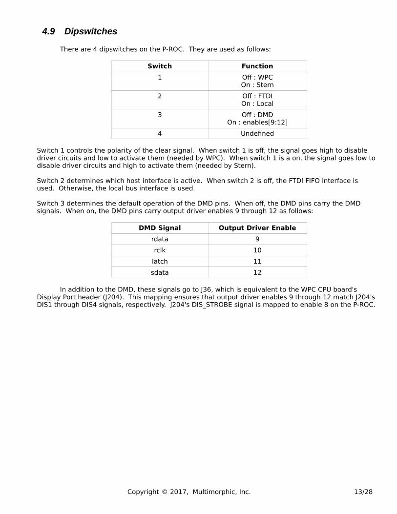
4.9 Dipswitches
There are 4 dipswitches on the P-ROC. They are used as follows:
Switch Function
1 Off : WPCOn : Stern
2 Off : FTDIOn : Local
3 Off : DMDOn : enables[9:12]
4 Undefined
Switch 1 controls the polarity of the clear signal. When switch 1 is off, the signal goes high to disable driver circuits and low to activate them (needed by WPC). When switch 1 is a on, the signal goes low todisable driver circuits and high to activate them (needed by Stern).
Switch 2 determines which host interface is active. When switch 2 is off, the FTDI FIFO interface is used. Otherwise, the local bus interface is used.
Switch 3 determines the default operation of the DMD pins. When off, the DMD pins carry the DMD signals. When on, the DMD pins carry output driver enables 9 through 12 as follows:
DMD Signal Output Driver Enable
rdata 9
rclk 10
latch 11
sdata 12
In addition to the DMD, these signals go to J36, which is equivalent to the WPC CPU board's Display Port header (J204). This mapping ensures that output driver enables 9 through 12 match J204's DIS1 through DIS4 signals, respectively. J204's DIS_STROBE signal is mapped to enable 8 on the P-ROC.
Copyright © 2017, Multimorphic, Inc. 13/28

4.10 Status
There are 3 power leds. When behaving normally, they should all on when the board has power.
LED Voltage Indication
D49 Switch Power(WPC: 12V, Stern: 5V)
D50 3.3V
D52 5V
There are 8 LEDs on the board to provide visual indications about the functionality of the board. The LEDs are driven by the FPGA as follows:
LED Meaning
D41 FPGA initialized properly
D42 12 Mhz clock operational
D43 USB communications established
D44 Watchdog timer expired(Drivers disabled)
D45 Pattern*
D46 Pattern*
D47 Pattern*
D48 Pattern*
* D45 through D48 display a rotating pattern. Normal operation is indicated by a single light rotating counter clockwise.
Copyright © 2017, Multimorphic, Inc. 14/28

4.11 Connectors
J1 WPC Direct Switch Inputsto Fliptronic II Board (J906)
6-pin Molex: 0.100” spacing
1 Direct Switch Input 0 I
2 KEY N/A
3 Direct Switch Input 2 I
4 Direct Switch Input 4 I
5 Direct Switch Input 6 I
6 Ground O
J2 WPC Direct Switch Inputsto Fliptronic II Board (J905)
6-pin Molex: 0.100” spacing
1 Direct Switch Input 1 I
2 Direct Switch Input 3 I
3 Direct Switch Input 5 I
4 KEY N/A
5 Direct Switch Input 7 I
6 Ground O
J3 Dot Matrix Display
24-pin Header: 0.100” spacing
1 Data Enable O 2 Ground O
3 Row Data O 4 Ground O
5 Row clock O 6 Ground O
7 Column Latch O 8 Ground O
9 Dot Clock O 10 Ground O
11 S Data O 12 Ground O
13 Ground O 14 Ground O
J4 WPC-x Output Driver Data/Enablesto Fliptronic II Board
36-pin Header 0.100” spacing
1 Output Driver Data 7 O 2 Ground O
3 Output Driver Data 6 O 4 Ground O
5 Output Driver Data 5 O 6 Ground O
7 Output Driver Data 4 O 8 Ground O
Copyright © 2017, Multimorphic, Inc. 15/28

9 Output Driver Data 3 O 10 Ground O
11 Output Driver Data 2 O 12 Ground O
13 Output Driver Data 1 O 14 Ground O
15 Output Driver Data 0 O 16 Ground O
17 VCC O 18 Ground O
19 Ground O 20 Ground O
21 VCC O 22 Ground O
23 Output Driver Enable 0 O 24 Ground O
25 Ground O 26 Ground O
27 Clear O 28 Ground O
29 Ground O 30 Ground O
31 Ground O 32 N/C N/A
33 NC N/A 34 N/C N/A
J5 USB
4-pin USB Type B
1 5B I
2 Data- I/O
3 Data+ I/O
4 Ground I
J6 Stern S.A.M.Switch Row Inputs 8-15
10-pin Molex: 0.156” spacing
1 Direct Switch Input 7 /Row 15
I
2 Direct Switch Input 6 /Row 14
I
3 Direct Switch Input 5 /Row 13
I
4 Direct Switch Input 4 /Row 12
I
5 KEY N/A
6 Direct Switch Input 3 /Row 11
I
7 Direct Switch Input 2 /Row 10
I
8 Direct Switch Input 1 /Row 9
I
9 Direct Switch Input 0 /Row 8
I
10 Ground O
Copyright © 2017, Multimorphic, Inc. 16/28

J7 Burst Switches
26-pin Header: 0.100” spacing
1 3.3V O 2 Burst Switch Driver 16 O
3 3.3V O 4 Burst Switch Driver 17 O
5 Burst Switch Driver 22 O 6 Burst Switch Driver 18 O
7 Ground O 8 Burst Switch Driver 19 O
9 Ground O 10 Burst Switch Driver 20 O
11 Ground O 12 Burst Switch Driver 21 O
13 Burst Switch Driver 23 O 14 Burst Switch Input 16 O
15 Ground O 16 Burst Switch Input 17 O
17 Ground O 18 Burst Switch Input 18 O
19 Ground O 20 Burst Switch Input 19 O
21 Burst Switch Input 23 O 22 Burst Switch Input 20 O
23 3.3V O 24 Burst Switch Input 21 O
25 3.3V O 26 Burst Switch Input 22 O
J8 Burst Switches
26-pin Header: 0.100” spacing
1 3.3V O 2 Burst Switch Driver 0 O
3 3.3V O 4 Burst Switch Driver 1 O
5 Burst Switch Driver 6 O 6 Burst Switch Driver 2 O
7 Ground O 8 Burst Switch Driver 3 O
9 Ground O 10 Burst Switch Driver 4 O
11 Ground O 12 Burst Switch Driver 5 O
13 Burst Switch Driver 7 O 14 Burst Switch Input 32 O
15 Ground O 16 Burst Switch Input 33 O
17 Ground O 18 Burst Switch Input 34 O
19 Ground O 20 Burst Switch Input 35 O
21 Burst Switch Input 39 O 22 Burst Switch Input 36 O
23 3.3V O 24 Burst Switch Input 37 O
25 3.3V O 26 Burst Switch Input 39 O
J9 Burst Switches
26-pin Header: 0.100” spacing
1 3.3V O 2 Burst Switch Driver 8 O
3 3.3V O 4 Burst Switch Driver 9 O
5 Burst Switch Driver 14 O 6 Burst Switch Driver 10 O
7 Ground O 8 Burst Switch Driver 11 O
9 Ground O 10 Burst Switch Driver 12 O
11 Ground O 12 Burst Switch Driver 13 O
Copyright © 2017, Multimorphic, Inc. 17/28

13 Burst Switch Driver 15 O 14 Burst Switch Input 8 O
15 Ground O 16 Burst Switch Input 9 O
17 Ground O 18 Burst Switch Input 10 O
19 Ground O 20 Burst Switch Input 11 O
21 Burst Switch Input 15 O 22 Burst Switch Input 12 O
23 3.3V O 24 Burst Switch Input 13 O
25 3.3V O 26 Burst Switch Input 14 O
J10 Burst Switches
26-pin Header: 0.100” spacing
1 3.3V O 2 Burst Switch Driver 24 O
3 3.3V O 4 Burst Switch Driver 25 O
5 Burst Switch Driver 30 O 6 Burst Switch Driver 26 O
7 Ground O 8 Burst Switch Driver 27 O
9 Ground O 10 Burst Switch Driver 28 O
11 Ground O 12 Burst Switch Driver 29 O
13 Burst Switch Driver 31 O 14 Burst Switch Input 56 O
15 Ground O 16 Burst Switch Input 57 O
17 Ground O 18 Burst Switch Input 58 O
19 Ground O 20 Burst Switch Input 59 O
21 Burst Switch Input 63 O 22 Burst Switch Input 60 O
23 3.3V O 24 Burst Switch Input 61 O
25 3.3V O 26 Burst Switch Input 62 O
J11 Burst Switches
26-pin Header: 0.100” spacing
1 3.3V O 2 Burst Switch Driver 16 O
3 3.3V O 4 Burst Switch Driver 17 O
5 Burst Switch Driver 22 O 6 Burst Switch Driver 18 O
7 Ground O 8 Burst Switch Driver 19 O
9 Ground O 10 Burst Switch Driver 20 O
11 Ground O 12 Burst Switch Driver 21 O
13 Burst Switch Driver 23 O 14 Burst Switch Input 48 O
15 Ground O 16 Burst Switch Input 49 O
17 Ground O 18 Burst Switch Input 50 O
19 Ground O 20 Burst Switch Input 51 O
21 Burst Switch Input 55 O 22 Burst Switch Input 52 O
23 3.3V O 24 Burst Switch Input 53 O
25 3.3V O 26 Burst Switch Input 54 O
Copyright © 2017, Multimorphic, Inc. 18/28

J12 Burst Switches
26-pin Header: 0.100” spacing
1 3.3V O 2 Burst Switch Driver 0 O
3 3.3V O 4 Burst Switch Driver 1 O
5 Burst Switch Driver 6 O 6 Burst Switch Driver 2 O
7 Ground O 8 Burst Switch Driver 3 O
9 Ground O 10 Burst Switch Driver 4 O
11 Ground O 12 Burst Switch Driver 5 O
13 Burst Switch Driver 7 O 14 Burst Switch Input 0 O
15 Ground O 16 Burst Switch Input 1 O
17 Ground O 18 Burst Switch Input 2 O
19 Ground O 20 Burst Switch Input 3 O
21 Burst Switch Input 7 O 22 Burst Switch Input 4 O
23 3.3V O 24 Burst Switch Input 5 O
25 3.3V O 26 Burst Switch Input 6 O
J13 Burst Switches
26-pin Header: 0.100” spacing
1 3.3V O 2 Burst Switch Driver 8 O
3 3.3V O 4 Burst Switch Driver 9 O
5 Burst Switch Driver 14 O 6 Burst Switch Driver 10 O
7 Ground O 8 Burst Switch Driver 11 O
9 Ground O 10 Burst Switch Driver 12 O
11 Ground O 12 Burst Switch Driver 13 O
13 Burst Switch Driver 15 O 14 Burst Switch Input 40 O
15 Ground O 16 Burst Switch Input 41 O
17 Ground O 18 Burst Switch Input 42 O
19 Ground O 20 Burst Switch Input 43 O
21 Burst Switch Input 47 O 22 Burst Switch Input 44 O
23 3.3V O 24 Burst Switch Input 45 O
25 3.3V O 26 Burst Switch Input 46 O
J14 Burst Switches
26-pin Header: 0.100” spacing
1 3.3V O 2 Burst Switch Driver 24 O
3 3.3V O 4 Burst Switch Driver 25 O
5 Burst Switch Driver 30 O 6 Burst Switch Driver 26 O
7 Ground O 8 Burst Switch Driver 27 O
9 Ground O 10 Burst Switch Driver 28 O
Copyright © 2017, Multimorphic, Inc. 19/28

11 Ground O 12 Burst Switch Driver 29 O
13 Burst Switch Driver 31 O 14 Burst Switch Input 24 O
15 Ground O 16 Burst Switch Input 25 O
17 Ground O 18 Burst Switch Input 26 O
19 Ground O 20 Burst Switch Input 27 O
21 Burst Switch Input 31 O 22 Burst Switch Input 27 O
23 3.3V O 24 Burst Switch Input 29 O
25 3.3V O 26 Burst Switch Input 30 O
J15 Stern Whitestar & S.A.M.Direct Switch Inputs
12-pin Molex: 0.156” spacing
1 Ground O
2 Direct Switch Input 8 I
3 Direct Switch Input 9 I
4 Direct Switch Input 10 I
5 KEY N/A
6 Direct Switch Input 11 I
7 Direct Switch Input 12 I
8 Direct Switch Input 13 I
9 Direct Switch Input 14 I
10 Direct Switch Input 15 I
11 Ground O
12 NC N/A
J16 WPC Switch Column/RowWPC-95 Switch Column/Row, Direct
13-pin Molex: 0.100” spacing
1 Column 1 O
2 Column 2 O
3 Column 3 O
4 Row 1 I
5 KEY N/A
6 Row 2 I
7 Row 3 I
8 Row 4 I
9 Direct Switch Input 0 I
10 Direct Switch Input 1 I
11 Direct Switch Input 2 I
Copyright © 2017, Multimorphic, Inc. 20/28

12 Direct Switch Input 3 I
13 Ground O
J17 Unused
J18 WPC Direct Switch Inputs
12-pin Molex: 0.100” spacing
1 Direct Switch Input 8 I
2 Direct Switch Input 9 I
3 Direct Switch Input 10 I
4 Direct Switch Input 11 I
5 NC N/A
6 Direct Switch Input 12 I
7 Direct Switch Input 13 I
8 Direct Switch Input 14 I
9 Direct Switch Input 15 I
10 Ground O
11 KEY N/A
12 Switch Clear O
J19/J20 WPC-x Switch Column Drivers
9-Pin Molex: 0.100” spacing
1 Column 0 O
2 Column 1 O
3 Column 2 O
4 Column 3 O
5 Column 4 O
6 Column 5 O
7 Column 6 O
8 KEY N/A
9 Column 7 O
J21 Stern Whitestar & S.A.M. Switch Column Drivers
9-Pin Molex: 0.156” spacing
1 Column 0 O
2 KEY N/A
3 Column 1 O
4 Column 2 O
5 Column 3 O
Copyright © 2017, Multimorphic, Inc. 21/28

6 Column 4 O
7 Column 5 O
8 Column 6 O
9 Column 7 O
J22 WPC-x Switch Row Inputs
9-pin Molex: 0.100” spacing
1 Row 0 I
2 Row 1 I
3 Row 2 I
4 Row 3 I
5 Row 4 I
6 KEY N/A
7 Row 5 I
8 Row 6 I
9 Row 7 I
J23 WPC Switch Row InputsWPC-95 Switch Row Inputs, Direct Inputs
14-pin Molex: 0.100” spacing
1 Row 0 I
2 Row 1 I
3 Row 2 I
4 Row 3 I
5 Row 4 I
6 KEY N/A
7 Row 5 I
8 Row 6 I
9 Row 7 I
10 Direct Switch Input 4 I
11 Direct Switch Input 5 I
12 Direct Switch Input 6 I
13 Direct Switch Input 7 I
14 Ground O
J24 Stern Whitestar & S.A.M.Switch Row Inputs 0-7
10-pin Molex: 0.156” spacing
1 Row 0 I
Copyright © 2017, Multimorphic, Inc. 22/28

2 Row 1 I
3 Row 2 I
4 KEY N/A
5 Row 3 I
6 Row 4 I
7 Row 5 I
8 Row 6 I
9 Row 7 I
10 Ground O
J25 Stern S.A.M. Direct Switch Inputs 24-31
10-pin Molex: 0.156” spacing
1 Direct Switch Input 24 I
2 KEY N/A
3 Direct Switch Input 25 I
4 Direct Switch Input 26 I
5 Direct Switch Input 27 I
6 Direct Switch Input 28 I
7 Direct Switch Input 29 I
8 Direct Switch Input 30 I
9 Direct Switch Input 31 I
10 Ground O
J26 Power
4-pin Molex: 0.200” spacing
1 12V I
2 Ground I
3 Ground I
4 VCC (5V) I
J27 WPC-x Output Driver Data/Enablesto Power Driver Board
34-pin Header: 0.100” spacing
1 NC N/A 2 Ground O
3 NC N/A 4 Ground O
5 NC N/A 6 Ground O
7 Output Driver Row Enable O 8 Output Driver Column Enable O
9 Output Driver Enable 2 O 10 Output Driver Enable 4 O
11 Output Driver Enable 3 O 12 Ouptut Driver Enable 1 O
Copyright © 2017, Multimorphic, Inc. 23/28

13 Output Driver Enable 5 O 14 Ground O
15 Output Driver Data 7 O 16 Ground O
17 Output Driver Data 6 O 18 Ground O
19 Output Driver Data 5 O 20 Ground O
21 Output Driver Data 4 O 22 Ground O
23 Output Driver Data 3 O 24 Ground O
25 Output Driver Data 2 O 26 Ground O
27 Output Driver Data 1 O 28 Ground O
29 Output Driver Data 0 O 30 Ground O
31 Clear O 32 Output Driver Enable 0* O
33 NC N/A 34 Enable_Strobe I
• Note – Pin 32 is connected to Jumper W2 on WPC Power Driver Boards and to the flipper driver enable on WPC-95 Power Driver Boards. For consistency across WPC and WPC-95, the flipper driver enable signal goes to the Fliptronic II board on WPC systems. Therefore, when using this board with a WPC Power Driver Board, disconnect jumper W2 to ensure proper operation of the Fliptronic II board. Failure to remove jumper W2 could create a short if the 18V power rail fails.
J28 Direct Output Drivers 0-15
26-pin Header: 0.100” spacing
1 3.3V O 2 3.3V O
3 Direct Output Driver 0 O 4 Direct Output Driver 1 O
5 Ground O 6 Direct Output Driver 2 O
7 Direct Output Driver 3 O 8 Direct Output Driver 4 O
9 Ground O 10 Direct Output Driver 5 O
11 Direct Output Driver 6 O 12 Direct Output Driver 7 O
13 Ground O 14 KEY O
15 Direct Output Driver 8 O 16 Direct Output Driver 9 O
17 Ground O 18 Direct Output Driver 10 O
19 Direct Output Driver 11 O 20 Direct Output Driver 12 O
21 Ground O 22 Direct Output Driver 13 O
23 Direct Output Driver 14 O 24 Direct Output Driver 15 O
25 3.3V O 26 3.3V O
J29 Direct Output Drivers 16-31
26-pin Header: 0.100” spacing
1 3.3V O 2 3.3V O
3 Direct Output Driver 16 O 4 Direct Output Driver 17 O
5 Ground O 6 Direct Output Driver 18 O
7 Direct Output Driver 19 O 8 Direct Output Driver 20 O
9 Ground O 10 Direct Output Driver 21 O
11 Direct Output Driver 22 O 12 Direct Output Driver 23 O
13 Ground O 14 KEY O
Copyright © 2017, Multimorphic, Inc. 24/28

15 Direct Output Driver 24 O 16 Direct Output Driver 25 O
17 Ground O 18 Direct Output Driver 26 O
19 Direct Output Driver 27 O 20 Direct Output Driver 28 O
21 Ground O 22 Direct Output Driver 29 O
23 Direct Output Driver 30 O 24 Direct Output Driver 31 O
25 3.3V O 26 3.3V O
J30 Stern Output Driver Data/Enablesto Power Driver Board
20-pin Header: 0.100” spacing
1 Output Driver Data 3 O 2 Output Driver Data 4 O
3 Output Driver Data 2 O 4 Output Driver Data 5 O
5 Output Driver Data 1 O 6 Output Driver Data 6 O
7 Output Driver Data 0 O 8 Output Driver Data 7 O
9 NC N/A 10 NC N/A
11 Output Driver Enable 7 O 12 Output Driver Enable 0 O
13 Clear O 14 Output Driver Enable 1 O
15 Output Driver Enable 5 / IOSTB O 16 Output Driver Enable 2 O
17 Output Driver Enable 4 O 18 Output Driver Enable 3 O
19 Ground O 20 Ground O
J31 Stern Whitestar & S.A.M. Power
6-pin Molex: 0.156” spacing
1 5V I
2 Ground I
3 -12V I
4 Ground I
5 KEY N/A
6 12V I
J32 WPC-x Power
7-pin Molex: 0.156” spacing
1 Ground I
2 NC N/A
3 Ground I
4 VCC (5V) I
5 VCC (5V) I
6 12V I
7 12V I
Copyright © 2017, Multimorphic, Inc. 25/28

J33 Stern S.A.M. Direct Switch Inputs 16-23
10-pin Molex: 0.156” spacing
1 Direct Switch Input 16 I
2 Direct Switch Input 17 I
3 KEY N/A
4 Direct Switch Input 18 I
5 Direct Switch Input 29 I
6 Direct Switch Input 20 I
7 Direct Switch Input 21 I
8 Direct Switch Input 22 I
9 Direct Switch Input 23 I
10 Ground O
J34 Local Interface (dipswitch 2 on)
16-pin Header: 0.100” spacing
1 Local Data 0 I/O
2 Ground O
3 Local Data 1 I/O
4 Ground O
5 Local Data 2 I/O
6 Ground O
7 Local Data 3 I/O
8 Ground O
9 Local Read I
10 Ground O
11 Local Write I
12 Ground O
13 Local Full O
14 Ground O
15 Local Empty O
16 Ground O
J34 Serial Driver Board Interface(dipswitch 2 off)
16-pin Header: 0.100” spacing
1 Serial Driver Board Data O
2 Ground O
3 RESERVED N/A
4 Ground O
5 RESERVED N/A
6 Ground O
7 RESERVED N/A
8 Ground O
9 RESERVED N/A
10 Ground O
11 RESERVED N/A
12 Ground O
13 RESERVED N/A
14 Ground O
15 RESERVED N/A
16 Ground O
J35 JTAG Port
14-pin Header: 2mm spacing
1 Ground O
2 3.3V O
Copyright © 2017, Multimorphic, Inc. 26/28

3 Ground O
4 TMS I
5 Ground O
6 TCK I
7 Ground O
8 TDO O
9 Ground O
10 TDI I
11 Ground O
12 Ground O
13 Ground O
14 Ground O
J36 WPC Display Port
26-pin Header: 2mm spacing
1 Output Driver Enable 12 O
2 Output Driver Enable 11 O
3 Output Driver Enable 10 O
4 Ground O
5 Output Driver Enable 9 O
4 Ground O
7 Output Driver Enable 8 O
8 Ground O
9 Clear O
10 Ground O
11 Data 7 O
12 Ground O
13 Data 6 O
14 Ground O
15 Data 5 O
16 Ground O
17 Data 4 O
18 Ground O
19 Data 3 O
20 Ground O
21 Data 2 O
22 Ground O
23 Data 1 O
24 Ground O
25 Data 0 O
26 Ground O
Copyright © 2017, Multimorphic, Inc. 27/28

4.12 Power
There are 3 power connectors that can be used to connect the 12V and 5V power rails. Only one should be used at any one time. J26 is pin compatible with a standard personal computer 4-pin power supply cable commonly used to power disk drives. J32 is pin compatible with the power supply cable used in WPC and WPC-95 pinball machines. J31 is pin compatible with the power supply cable used in Stern Whitestar and S.A.M. pinball machines.
3.3V is created from the 5V supply using a 3 amp LDO in a DD-PACK package. Components are available from ST Micro, Linear Tech, TI, and National Semi. 3.3V is used by most of the parts on the board. In addition, external burst switch circuitry is expected to use 3.3V from this board.
1.2V is created from the 5V supply using a 300 milliamp LDO in a SOT23-5 package. Components are available from On Semi and Analog Devices. 1.2V is used for the FPGA's core.
5V is optionally used to power the 74HCT244 buffers used on the output driver data/enables bus and the dot matrix display signals. Resistor stuff options allow the buffers to alternatively run on 3.3V. Which voltage to use depends on the circuitry connected to J3, J4, J27, and J30.
The switch voltage depends on which power connector is used to power the board. WPC machines use a 12V switch matrix; so if J26 or J32 is used, the incoming 12V powers the switch voltage. Stern machines use a 5V switch matrix; so if J31 is used, its 12V feeds a 5V LDO, which creates the switch voltage.
Copyright © 2017, Multimorphic, Inc. 28/28