pin assignments enable truth table - ti.com
TRANSCRIPT

1FEATURESDESCRIPTION
APPLICATIONS
PIN ASSIGNMENTSAI
AO
BO
CO
DO
AIAI
BI
BI
C1
C1
D1
D1D1
E2
E1
123
4 5678
161514
131211109
AIAI
AOE1BOBIBI
GND
VCCDIDIDOE2COCICI
SOIC PACKAGE(TOP VIEW)
Enable Truth Table
TB5R3
SLLS643A–SEPTEMBER 2005–REVISED OCTOBER 2007www.ti.com
QUAD DIFFERENTIAL PECL RECEIVERS
• Functional Replacement for the Agere BRF1A• Pin Equivalent to General Trade 26LS32 These quad differential receivers accept digital data
over balanced transmission lines. They translate• High Input Impedance Approximately 8 kΩdifferential input logic levels to TTL output logic
• <2.6-ns Maximum Propagation Delay levels.• TB5R3 Provides 50-mV Hysteresis (Typical)
The TB5R3 is a pin- and function-compatible• -1.1-V to 7.1-V Common-Mode Input Voltage replacement for the Agere systems BRF1A; it
Range includes 3-kV HBM and 2-kV CDM ESD protection.• Single 5-V ±10% Supply The power-down loading characteristics of the• ESD Protection HBM > 3 kV and CDM > 2 kV receiver input circuit are approximately 8 kΩ relative
to the power supplies; hence they do not load the• Operating Temperature Range: -40°C to 85°Ctransmission line when the circuit is powered down.• Available in Gull-Wing SOIC (JEDEC MS-013,
DW) and SOIC (D) Package The packaging for this differential line receiver is a16-pin gull wing SOIC (DW) or a 16 pin SOIC (D).
The enable inputs of this device include internal• Digital Data or Clock Transmission Over pull-up resistors of approximately 40 kΩ that are
Balanced Lines connected to VCC to ensure a logical high level inputif the inputs are open circuited.
FUNCTIONAL BLOCK DIAGRAM
OUTPUTE1 E2 CONDITION0 0 Active1 0 Active0 1 Disabled1 1 Active
1
Please be aware that an important notice concerning availability, standard warranty, and use in critical applications ofTexas Instruments semiconductor products and disclaimers thereto appears at the end of this data sheet.
PRODUCTION DATA information is current as of publication date. Copyright © 2005–2007, Texas Instruments IncorporatedProducts conform to specifications per the terms of the TexasInstruments standard warranty. Production processing does notnecessarily include testing of all parameters.

www.ti.com
POWER DISSIPATION RATINGS
ABSOLUTE MAXIMUM RATINGS
TB5R3
SLLS643A–SEPTEMBER 2005–REVISED OCTOBER 2007
These devices have limited built-in ESD protection. The leads should be shorted together or the device placed in conductive foamduring storage or handling to prevent electrostatic damage to the MOS gates.
ORDERING INFORMATIONPART NUMBER (1) PART MARKING PACKAGE (2) LEAD FINISH STATUS
TB5R3DW TB5R3 Gull-Wing SOIC NiPdAu ProductionTB5R3D TB5R3 SOIC NiPdAu Production
(1) Add the R suffix for tape and reel carrier (i.e., TB5R3DR)(2) For the most current package and ordering information, see the Package Option Addendum at the end of this document, or see the TI
website at www.ti.com.
THERMAL RESISTANCE, DERATINGCIRCUIT BOARD POWER RATING POWER RATINGPACKAGE JUNCTION-TO-AMBIENT FACTOR (1)MODEL TA ≤ 25°C TA = 85°CWITH NO AIR FLOW TA ≥ 25°CLow-K (2) 831 mW 120.3°C/W 8.3 mW/°C 332 mW
DWHigh-K (3) 1240 mW 80.8°C/W 12.4 mW/°C 494 mWLow-K (2) 763 mW 131.1°C/W 7.6 mW/°C 305 mW
DHigh-K (3) 1190 mW 84.1°C/W 11.9 mW/°C 475 mW
(1) This is the inverse of the junction-to-ambient thermal resistance when board-mounted with no air flow.(2) In accordance with the low-K thermal metric definitions of EIA/JESD51-3.(3) In accordance with the high-K thermal metric definitions of EIA/JESD51-7.
THERMAL CHARACTERISTICSPARAMETER PACKAGE VALUE UNIT
DW 53.7θJB Junction-to-Board Thermal Resistance °C/W
D 47.5DW 47.1
θJC Junction-to-Case Thermal Resistance °C/WD 44.2
over operating free-air temperature range unless otherwise noted (1)
UNITSupply voltage, VCC 0 V to 6 VMagnitude of differential bus (input) voltage, |VAI - VAI|, |VBI - VBI|, |VCI - VCI|, |VDI - VDI| 8.4 V
Human Body Model (2) All pins ±3.5 kVESD
Charged-Device Model (3) All pins ±2 kVContinuous power dissipation See Dissipation Rating TableStorage temperature, Tstg -65°C to 150°C
(1) Stresses beyond those listed under "absolute maximum ratings” may cause permanent damage to the device. These are stress ratingsonly, and functional operation of the device at these or any other conditions beyond those indicated under "recommended operatingconditions” is not implied. Exposure to absolute-maximum-rated conditions for extended periods may affect device reliability.
(2) Tested in accordance with JEDEC Standard 22, Test Method A114-A.(3) Tested in accordance with JEDEC Standard 22, Test Method C101.
2 Submit Documentation Feedback Copyright © 2005–2007, Texas Instruments Incorporated
Product Folder Link(s): TB5R3

www.ti.com
RECOMMENDED OPERATING CONDITIONS
DEVICE ELECTRICAL CHARACTERISTICS
RECEIVER ELECTRICAL CHARACTERISTICS
TB5R3
SLLS643A–SEPTEMBER 2005–REVISED OCTOBER 2007
MIN NOM MAX UNITSupply voltage, VCC 4.5 5 5.5 VBus pin input voltage, VAI, VAI, VBIVBI, VCI , or VCI, VDI, VDI -1.2 (1) 7.2 VMagnitude of differential input voltage, |VAI - VAI|, |VBI - VBI|, |VCI - VCI|, |VDI - VDI| 0.1 6 VLow-level enable input voltage (2), VIL (VCC = 5.5 V) 0.8 VHigh-level enable input voltage (2), VIH (VCC = 5.5 V) 2 VOperating free-air temperature, TA -40 85 °C
(1) The algebraic convention, in which the least positive (most negative) limit is designated as minimum is used in this data sheet, unlessotherwise noted.
(2) The input levels and difference voltage provide no noise immunity and should be tested only in a static, noise-free environment.
over operating free-air temperature range unless otherwise noted
PARAMETER TEST CONDITIONS MIN TYP MAX UNITOutputs disabled 50 mA
ICC Supply current (1)Outputs enabled 48 mA
(1) Current is dc power draw as measured through GND pin and does not include power delivered to load.
over operating free-air temperature range unless otherwise noted
PARAMETER TEST CONDITIONS MIN TYP MAX UNITVOL Output low voltage VCC = 4.5 V, IOL = 8 mA 0.4 VVOH Output high voltage VCC = 4.5 V, IOH = -400 µA 2.4 VVIK Enable input clamp voltage VCC = 4.5 V, II = -5 mA -1 (1) VVTH+ Positive-going differential input threshold voltage (2), (Vxl - VxI) x = A, B, C, or D 100 mV
-VTH- Negative-going differential input threshold voltage (2), (Vxl - VxI) x = A, B, C, or D mV100 (1)
VHYST Differential input threshold voltage hysteresis, (VTH+ - VTH–) 50 mVIOZL VO = 0.4 V -20 (1) µA
Output off-state current, (High-Z) VCC = 5.5 VIOZH VO = 2.4 V 20 µA
-IOS Output short circuit current VCC = 5.5 V mA400 (1)
-IIL Enable input low current VCC = 5.5 V, VIN = 0.4 V µA400 (1)
Enable input high current VIN = 2.7 V 20 µAIIH VCC = 5.5 V
Enable input reverse current VIN = 5.5 V 100 µAIIL Differential input low current VCC = 5.5V, VIN = -1.2 V -2 (1) mAIIH Differential input high current VCC= 5.5V, VIN = 7.2 V 1 mA
Output High 50RO Small-signal output resistance Ω
Output Low 25
(1) This parameter is listed using a magnitude and polarity/direction convention, rather than an algebraic convention, to match the originalAgere data sheet.
(2) The input levels and difference voltage provide no noise immunity and should be tested only in a static, noise-free environment.
Copyright © 2005–2007, Texas Instruments Incorporated Submit Documentation Feedback 3
Product Folder Link(s): TB5R3
www.ti.com
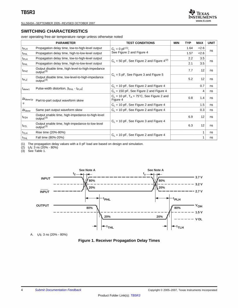
SWITCHING CHARACTERISTICS
OUTPUT
3.7 V
2.7 V
3.2 V
VOH
V OL
1.5 V
tTHL
tPHL tPLH
tTLH
20%
80%
20%
80%
INPUT
INPUT
See Note A See Note Atf tr
80% 80%
20% 20%
TB5R3
SLLS643A–SEPTEMBER 2005–REVISED OCTOBER 2007
over operating free-air temperature range unless otherwise noted
PARAMETER TEST CONDITIONS MIN TYP MAX UNITtPLH Propagation delay time, low-to-high-level output 1.64 <2.6CL = 0 pF (1), nsSee Figure 2 and Figure 4tPHL Propagation delay time, high-to-low-level output 1.57 <2.6tPLH Propagation delay time, low-to-high-level output 2.2 3.5
CL = 50 pF, See Figure 2 and Figure 4 (2) nstPHL Propagation delay time, high-to-low-level output 2.1 3.5
Output disable time, high-level-to-high-impedancetPHZ 7.7 12 nsoutput (3)CL = 5 pF, See Figure 3 and Figure 5
Output disable time, low-level-to-high-impedancetPLZ 5.2 12 nsoutput (3)
CL = 10 pF, See Figure 2 and Figure 4 0.7 nstskew1 Pulse-width distortion, |tPHL - tPLH|
CL = 150 pF, See Figure 2 and Figure 4 4 nsCL = 10 pF, TA = 75°C, See Figure 2 and 0.8 1.4 nsΔtskew1p Figure 4Part-to-part output waveform skew
-p CL = 10 pF, See Figure 2 and Figure 4 1.5 nsΔtskew Same part output waveform skew CL = 10 pF, See Figure 2 and Figure 4 0.3 ns
Output enable time, high-impedance-to-high-leveltPZH 6.9 12 nsoutput (3)CL = 10 pF, See Figure 3 and Figure 4
Output enable time, high-impedance-to-low-leveltPZL 6.3 12 nsoutput (3)
tTLH Rise time (20%-80%) 1 nsCL = 10 pF, See Figure 2 and Figure 4
tTHL Fall time (80%-20%) 1 ns
(1) The propagation delay values with a 0 pF load are based on design and simulation.(2) tr/tf: 3 ns (20% - 80%)(3) See Table 1.
A. tr/tf: 3 ns (20% - 80%)
Figure 1. Receiver Propagation Delay Times
4 Submit Documentation Feedback Copyright © 2005–2007, Texas Instruments Incorporated
Product Folder Link(s): TB5R3
www.ti.com
OUTPUT
2.4 V
0.4 V
1.5 V
tPHZ tPZH tPLZ tPZL
0.2 V0.2 V
0.2 V0.2 V
0.4 V
2.4 V
1.5 V
E2See
Note A
E1See
Note B
VOH
VOL
TO OUTPUTOF DEVICEUNDER TEST
5 V
5 k
DIODES TYPE458E, 1N4148,OR EQUIVALENT
2 k
CL
CL includes test-fixture and probe capacitance.
TO OUTPUTOF DEVICEUNDER TEST
CL
500
1.5 V
CL includes test-fixture and probe capacitance.
TB5R3
SLLS643A–SEPTEMBER 2005–REVISED OCTOBER 2007
A. E2 = 1 while E1 changes states.B. E1 = 0 while E2 changes states.
Figure 2. Receiver Enable and Disable Timing
Parametric values specified under the Electrical Characteristics and Timing Characteristics sections for the datatransmission driver devices are measured with the following output load circuits.
Figure 3. Receiver Propagation Delay Time and Enable Time (tPZH, tPZL) Test Circuit
Figure 4. Receiver Disable Time (tPHZ, tPLZ) Test Circuit
Copyright © 2005–2007, Texas Instruments Incorporated Submit Documentation Feedback 5
Product Folder Link(s): TB5R3

www.ti.com
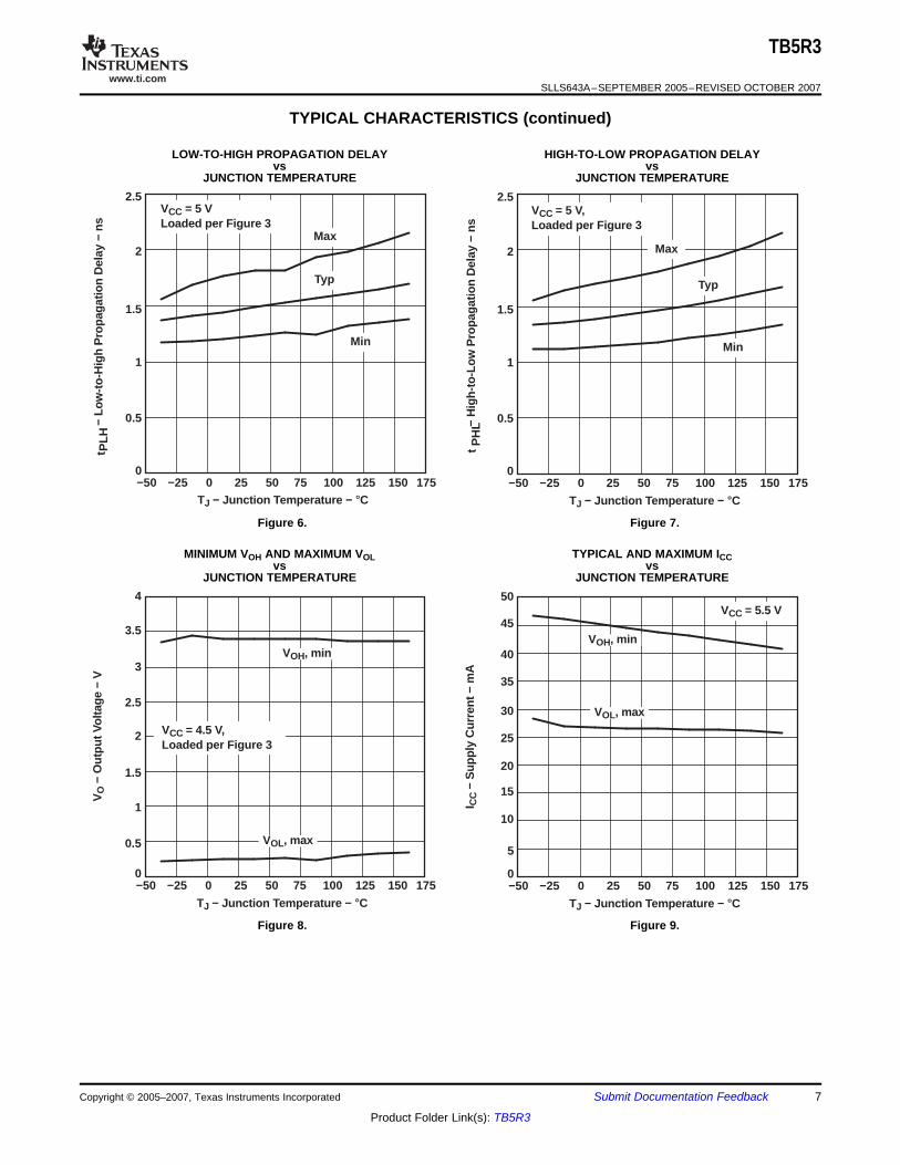
TYPICAL CHARACTERISTICS
0
2
4
3.5
3
2.5
0 50 100 150 200
t pd
− P
ropa
gatio
n D
elay
Tim
e −
ns
CL − Load Capacitance − pF2251751257525
1.5
1
0.5
tPLH
tPHL
TB5R3
SLLS643A–SEPTEMBER 2005–REVISED OCTOBER 2007
TYPICAL PROPAGATION DELAYvs
LOAD CAPACITANCE
NOTE: This graph is included as an aid to the system designers. Total circuit delay varies with load capacitance. The total delay is thesum of the delay due to external capacitance and the intrinsic delay of the device. Intrinsic delay is listed in the table above as the 0pF load condition. The incremental increase in delay between the 0 pF load condition and the actual total load capacitancerepresents the extrinsic, or external delay contributed by the load.
Figure 5.
6 Submit Documentation Feedback Copyright © 2005–2007, Texas Instruments Incorporated
Product Folder Link(s): TB5R3
www.ti.com
0
0.5
1
1.5
2.5
−50 0 50 100 150
− Lo
w-to
-Hig
h P
ropa
gatio
n D
elay
− n
st P
LH
TJ − Junction T emperature − C25−25 75 125 175
2Max
Typ
Min
VCC = 5 VLoaded per Figure 3
− H
igh-
to-L
ow P
ropa
gatio
n D
elay
− n
st
PH
L0
0.5
1
1.5
2.5
−50 0 50 100 150
TJ − Junction T emperature − C
25−25 75 125 175
2
VCC = 5 V,Loaded per Figure 3
Typ
Min
Max
0
0.5
1
1.5
2.5
−50 0 50 100 150
TJ − Junction T emperature − C
25−25 75 125 175
2
VO
− O
utpu
t Vol
tage
− V
3.5
3
4
VCC = 4.5 V,Loaded per Figure 3
VOH, min
VOL, max
0
5
10
15
25
−50 0 50 100 150
TJ − Junction T emperature − C
25−25 75 125 175
20
I CC
− S
uppl
y C
urre
nt −
mA 35
30
50VCC = 5.5 V
VOH, min
VOL, max
40
45
TB5R3
SLLS643A–SEPTEMBER 2005–REVISED OCTOBER 2007
TYPICAL CHARACTERISTICS (continued)
LOW-TO-HIGH PROPAGATION DELAY HIGH-TO-LOW PROPAGATION DELAYvs vs
JUNCTION TEMPERATURE JUNCTION TEMPERATURE
Figure 6. Figure 7.
MINIMUM VOH AND MAXIMUM VOL TYPICAL AND MAXIMUM ICCvs vs
JUNCTION TEMPERATURE JUNCTION TEMPERATURE
Figure 8. Figure 9.
Copyright © 2005–2007, Texas Instruments Incorporated Submit Documentation Feedback 7
Product Folder Link(s): TB5R3
www.ti.com
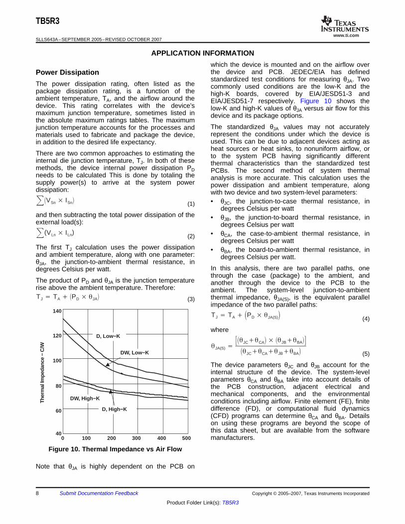
APPLICATION INFORMATION
Power Dissipation
VSn ISn
(1)
(VLn ILn) (2)
TJ TA PD JA (3)
TJ TA PD JA(S)
(4)
JA(S) JCCA
JBBA
JCCAJBBA (5)
40
60
80
100
120
140
0 100 200 300 400 500
Ther
mal
Impe
danc
e −
C/W
D, Low−K
DW, Low−K
DW, High−K
D, High−K
TB5R3
SLLS643A–SEPTEMBER 2005–REVISED OCTOBER 2007
which the device is mounted and on the airflow overthe device and PCB. JEDEC/EIA has definedstandardized test conditions for measuring θJA. Two
The power dissipation rating, often listed as the commonly used conditions are the low-K and thepackage dissipation rating, is a function of the high-K boards, covered by EIA/JESD51-3 andambient temperature, TA, and the airflow around the EIA/JESD51-7 respectively. Figure 10 shows thedevice. This rating correlates with the device's low-K and high-K values of θJA versus air flow for thismaximum junction temperature, sometimes listed in device and its package options.the absolute maximum ratings tables. The maximum
The standardized θJA values may not accuratelyjunction temperature accounts for the processes andrepresent the conditions under which the device ismaterials used to fabricate and package the device,used. This can be due to adjacent devices acting asin addition to the desired life expectancy.heat sources or heat sinks, to nonuniform airflow, or
There are two common approaches to estimating the to the system PCB having significantly differentinternal die junction temperature, TJ. In both of these thermal characteristics than the standardized testmethods, the device internal power dissipation PD PCBs. The second method of system thermalneeds to be calculated This is done by totaling the analysis is more accurate. This calculation uses thesupply power(s) to arrive at the system power power dissipation and ambient temperature, alongdissipation: with two device and two system-level parameters:
• θJC, the junction-to-case thermal resistance, indegrees Celsius per watt
and then subtracting the total power dissipation of the • θJB, the junction-to-board thermal resistance, inexternal load(s): degrees Celsius per watt
• θCA, the case-to-ambient thermal resistance, indegrees Celsius per watt
The first TJ calculation uses the power dissipation • θBA, the board-to-ambient thermal resistance, inand ambient temperature, along with one parameter: degrees Celsius per watt.θJA, the junction-to-ambient thermal resistance, in
In this analysis, there are two parallel paths, onedegrees Celsius per watt.through the case (package) to the ambient, and
The product of PD and θJA is the junction temperature another through the device to the PCB to therise above the ambient temperature. Therefore: ambient. The system-level junction-to-ambient
thermal impedance, θJA(S), is the equivalent parallelimpedance of the two parallel paths:
where
The device parameters θJC and θJB account for theinternal structure of the device. The system-levelparameters θCA and θBA take into account details ofthe PCB construction, adjacent electrical andmechanical components, and the environmentalconditions including airflow. Finite element (FE), finitedifference (FD), or computational fluid dynamics(CFD) programs can determine θCA and θBA. Detailson using these programs are beyond the scope ofthis data sheet, but are available from the softwaremanufacturers.
Figure 10. Thermal Impedance vs Air Flow
Note that θJA is highly dependent on the PCB on
8 Submit Documentation Feedback Copyright © 2005–2007, Texas Instruments Incorporated
Product Folder Link(s): TB5R3
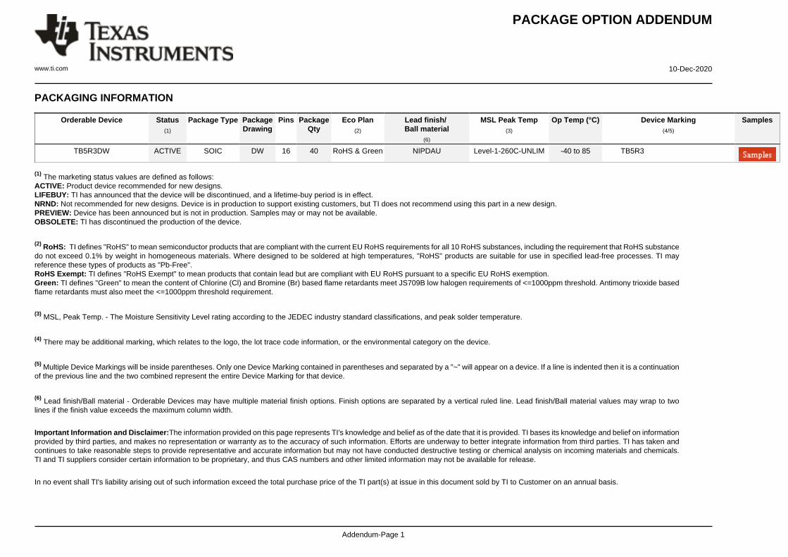
PACKAGE OPTION ADDENDUM
www.ti.com 10-Dec-2020
Addendum-Page 1
PACKAGING INFORMATION
Orderable Device Status(1)
Package Type PackageDrawing
Pins PackageQty
Eco Plan(2)
Lead finish/Ball material
(6)
MSL Peak Temp(3)
Op Temp (°C) Device Marking(4/5)
Samples
TB5R3DW ACTIVE SOIC DW 16 40 RoHS & Green NIPDAU Level-1-260C-UNLIM -40 to 85 TB5R3
(1) The marketing status values are defined as follows:ACTIVE: Product device recommended for new designs.LIFEBUY: TI has announced that the device will be discontinued, and a lifetime-buy period is in effect.NRND: Not recommended for new designs. Device is in production to support existing customers, but TI does not recommend using this part in a new design.PREVIEW: Device has been announced but is not in production. Samples may or may not be available.OBSOLETE: TI has discontinued the production of the device.
(2) RoHS: TI defines "RoHS" to mean semiconductor products that are compliant with the current EU RoHS requirements for all 10 RoHS substances, including the requirement that RoHS substancedo not exceed 0.1% by weight in homogeneous materials. Where designed to be soldered at high temperatures, "RoHS" products are suitable for use in specified lead-free processes. TI mayreference these types of products as "Pb-Free".RoHS Exempt: TI defines "RoHS Exempt" to mean products that contain lead but are compliant with EU RoHS pursuant to a specific EU RoHS exemption.Green: TI defines "Green" to mean the content of Chlorine (Cl) and Bromine (Br) based flame retardants meet JS709B low halogen requirements of <=1000ppm threshold. Antimony trioxide basedflame retardants must also meet the <=1000ppm threshold requirement.
(3) MSL, Peak Temp. - The Moisture Sensitivity Level rating according to the JEDEC industry standard classifications, and peak solder temperature.
(4) There may be additional marking, which relates to the logo, the lot trace code information, or the environmental category on the device.
(5) Multiple Device Markings will be inside parentheses. Only one Device Marking contained in parentheses and separated by a "~" will appear on a device. If a line is indented then it is a continuationof the previous line and the two combined represent the entire Device Marking for that device.
(6) Lead finish/Ball material - Orderable Devices may have multiple material finish options. Finish options are separated by a vertical ruled line. Lead finish/Ball material values may wrap to twolines if the finish value exceeds the maximum column width.
Important Information and Disclaimer:The information provided on this page represents TI's knowledge and belief as of the date that it is provided. TI bases its knowledge and belief on informationprovided by third parties, and makes no representation or warranty as to the accuracy of such information. Efforts are underway to better integrate information from third parties. TI has taken andcontinues to take reasonable steps to provide representative and accurate information but may not have conducted destructive testing or chemical analysis on incoming materials and chemicals.TI and TI suppliers consider certain information to be proprietary, and thus CAS numbers and other limited information may not be available for release.
In no event shall TI's liability arising out of such information exceed the total purchase price of the TI part(s) at issue in this document sold by TI to Customer on an annual basis.
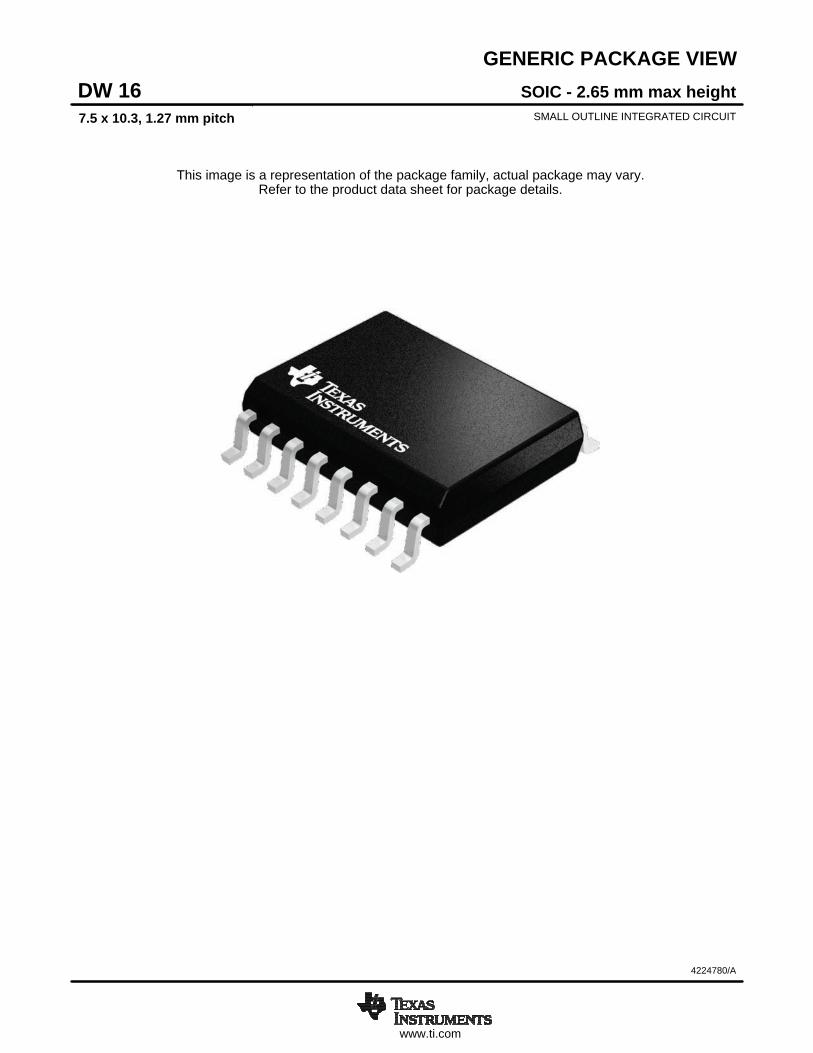
www.ti.com
GENERIC PACKAGE VIEW
This image is a representation of the package family, actual package may vary.Refer to the product data sheet for package details.
SOIC - 2.65 mm max heightDW 16SMALL OUTLINE INTEGRATED CIRCUIT7.5 x 10.3, 1.27 mm pitch
4224780/A
www.ti.com
PACKAGE OUTLINE
C
TYP10.639.97
2.65 MAX
14X 1.27
16X 0.510.31
2X8.89
TYP0.330.10
0 - 80.30.1
(1.4)
0.25GAGE PLANE
1.270.40
A
NOTE 3
10.510.1
BNOTE 4
7.67.4
4220721/A 07/2016
SOIC - 2.65 mm max heightDW0016ASOIC
NOTES: 1. All linear dimensions are in millimeters. Dimensions in parenthesis are for reference only. Dimensioning and tolerancing per ASME Y14.5M. 2. This drawing is subject to change without notice. 3. This dimension does not include mold flash, protrusions, or gate burrs. Mold flash, protrusions, or gate burrs shall not exceed 0.15 mm, per side. 4. This dimension does not include interlead flash. Interlead flash shall not exceed 0.25 mm, per side.5. Reference JEDEC registration MS-013.
1 16
0.25 C A B
98
PIN 1 IDAREA
SEATING PLANE
0.1 C
SEE DETAIL A
DETAIL ATYPICAL
SCALE 1.500

www.ti.com
EXAMPLE BOARD LAYOUT
0.07 MAXALL AROUND
0.07 MINALL AROUND
(9.3)
14X (1.27)
R0.05 TYP
16X (2)
16X (0.6)
4220721/A 07/2016
SOIC - 2.65 mm max heightDW0016ASOIC
NOTES: (continued) 6. Publication IPC-7351 may have alternate designs. 7. Solder mask tolerances between and around signal pads can vary based on board fabrication site.
METAL SOLDER MASKOPENING
NON SOLDER MASKDEFINED
SOLDER MASK DETAILS
OPENINGSOLDER MASK METAL
SOLDER MASKDEFINED
LAND PATTERN EXAMPLESCALE:7X
SYMM
1
8 9
16
SEEDETAILS
SYMM

www.ti.com
EXAMPLE STENCIL DESIGN
R0.05 TYP
16X (2)
16X (0.6)
14X (1.27)
(9.3)
4220721/A 07/2016
SOIC - 2.65 mm max heightDW0016ASOIC
NOTES: (continued) 8. Laser cutting apertures with trapezoidal walls and rounded corners may offer better paste release. IPC-7525 may have alternate design recommendations. 9. Board assembly site may have different recommendations for stencil design.
SOLDER PASTE EXAMPLEBASED ON 0.125 mm THICK STENCIL
SCALE:7X
SYMM
SYMM
1
8 9
16

IMPORTANT NOTICE AND DISCLAIMER
TI PROVIDES TECHNICAL AND RELIABILITY DATA (INCLUDING DATASHEETS), DESIGN RESOURCES (INCLUDING REFERENCE DESIGNS), APPLICATION OR OTHER DESIGN ADVICE, WEB TOOLS, SAFETY INFORMATION, AND OTHER RESOURCES “AS IS” AND WITH ALL FAULTS, AND DISCLAIMS ALL WARRANTIES, EXPRESS AND IMPLIED, INCLUDING WITHOUT LIMITATION ANY IMPLIED WARRANTIES OF MERCHANTABILITY, FITNESS FOR A PARTICULAR PURPOSE OR NON-INFRINGEMENT OF THIRD PARTY INTELLECTUAL PROPERTY RIGHTS.These resources are intended for skilled developers designing with TI products. You are solely responsible for (1) selecting the appropriate TI products for your application, (2) designing, validating and testing your application, and (3) ensuring your application meets applicable standards, and any other safety, security, or other requirements. These resources are subject to change without notice. TI grants you permission to use these resources only for development of an application that uses the TI products described in the resource. Other reproduction and display of these resources is prohibited. No license is granted to any other TI intellectual property right or to any third party intellectual property right. TI disclaims responsibility for, and you will fully indemnify TI and its representatives against, any claims, damages, costs, losses, and liabilities arising out of your use of these resources.TI’s products are provided subject to TI’s Terms of Sale (www.ti.com/legal/termsofsale.html) or other applicable terms available either on ti.com or provided in conjunction with such TI products. TI’s provision of these resources does not expand or otherwise alter TI’s applicable warranties or warranty disclaimers for TI products.
Mailing Address: Texas Instruments, Post Office Box 655303, Dallas, Texas 75265Copyright © 2020, Texas Instruments Incorporated