pickit™ 3 debug express pic18f45k20 – mplab c...
TRANSCRIPT

© 2009 Microchip Technology Inc. DS41370B
PICkit™ 3 Debug ExpressPIC18F45K20 – MPLAB® C Lessons
Note the following details of the code protection feature on Microchip devices:• Microchip products meet the specification contained in their particular Microchip Data Sheet.
• Microchip believes that its family of products is one of the most secure families of its kind on the market today, when used in the intended manner and under normal conditions.
• There are dishonest and possibly illegal methods used to breach the code protection feature. All of these methods, to our knowledge, require using the Microchip products in a manner outside the operating specifications contained in Microchip’s Data Sheets. Most likely, the person doing so is engaged in theft of intellectual property.
• Microchip is willing to work with the customer who is concerned about the integrity of their code.
• Neither Microchip nor any other semiconductor manufacturer can guarantee the security of their code. Code protection does not mean that we are guaranteeing the product as “unbreakable.”
Code protection is constantly evolving. We at Microchip are committed to continuously improving the code protection features of ourproducts. Attempts to break Microchip’s code protection feature may be a violation of the Digital Millennium Copyright Act. If such actsallow unauthorized access to your software or other copyrighted work, you may have a right to sue for relief under that Act.
Information contained in this publication regarding deviceapplications and the like is provided only for your convenienceand may be superseded by updates. It is your responsibility toensure that your application meets with your specifications.MICROCHIP MAKES NO REPRESENTATIONS ORWARRANTIES OF ANY KIND WHETHER EXPRESS ORIMPLIED, WRITTEN OR ORAL, STATUTORY OROTHERWISE, RELATED TO THE INFORMATION,INCLUDING BUT NOT LIMITED TO ITS CONDITION,QUALITY, PERFORMANCE, MERCHANTABILITY ORFITNESS FOR PURPOSE. Microchip disclaims all liabilityarising from this information and its use. Use of Microchipdevices in life support and/or safety applications is entirely atthe buyer’s risk, and the buyer agrees to defend, indemnify andhold harmless Microchip from any and all damages, claims,suits, or expenses resulting from such use. No licenses areconveyed, implicitly or otherwise, under any Microchipintellectual property rights.
DS41370B-page ii
Trademarks
The Microchip name and logo, the Microchip logo, Accuron, dsPIC, KEELOQ, KEELOQ logo, MPLAB, PIC, PICmicro, PICSTART, rfPIC, SmartShunt and UNI/O are registered trademarks of Microchip Technology Incorporated in the U.S.A. and other countries.
FilterLab, Linear Active Thermistor, MXDEV, MXLAB, SEEVAL, SmartSensor and The Embedded Control Solutions Company are registered trademarks of Microchip Technology Incorporated in the U.S.A.
Analog-for-the-Digital Age, Application Maestro, CodeGuard, dsPICDEM, dsPICDEM.net, dsPICworks, dsSPEAK, ECAN, ECONOMONITOR, FanSense, In-Circuit Serial Programming, ICSP, ICEPIC, Mindi, MiWi, MPASM, MPLAB Certified logo, MPLIB, MPLINK, mTouch, PICkit, PICDEM, PICDEM.net, PICtail, PIC32 logo, PowerCal, PowerInfo, PowerMate, PowerTool, REAL ICE, rfLAB, Select Mode, Total Endurance, WiperLock and ZENA are trademarks of Microchip Technology Incorporated in the U.S.A. and other countries.
SQTP is a service mark of Microchip Technology Incorporated in the U.S.A.
All other trademarks mentioned herein are property of their respective companies.
© 2009, Microchip Technology Incorporated, Printed in the U.S.A., All Rights Reserved.
Printed on recycled paper.
© 2009 Microchip Technology Inc.
Microchip received ISO/TS-16949:2002 certification for its worldwide headquarters, design and wafer fabrication facilities in Chandler and Tempe, Arizona; Gresham, Oregon and design centers in California and India. The Company’s quality system processes and procedures are for its PIC® MCUs and dsPIC® DSCs, KEELOQ® code hopping devices, Serial EEPROMs, microperipherals, nonvolatile memory and analog products. In addition, Microchip’s quality system for the design and manufacture of development systems is ISO 9001:2000 certified.

PICkit™ 3 DEBUG EXPRESS
Table of Contents
Chapter 1. Introduction1.1 Before Beginning the Lessons ....................................................................... 7
Chapter 2. PIC18FXXXX Microcontroller Architectural Overview 2.1 Memory Organization ..................................................................................... 92.2 Program Memory ............................................................................................ 9
2.2.1 Data Memory ............................................................................................. 102.2.2 Special Function Registers ........................................................................ 102.2.3 Return Address Stack ............................................................................... 10
Chapter 3. PICkit™ 3 Debug Express Lessons3.1 Lesson 1: Hello LED ..................................................................................... 11
3.1.1 Creating the Lesson 1 Project in the MPLAB® IDE .................................. 113.1.1.1 Step One: Select a device ......................................................... 113.1.1.2 Step Two: Select a language toolsuite ...................................... 123.1.1.3 Step Three: Create a new project .............................................. 133.1.1.4 Step Four: Add existing files to your project .............................. 133.1.1.5 Summary ................................................................................... 14
3.1.2 Exploring the Lesson 1 Source Code ........................................................ 163.1.3 Building and Programming the Lesson 1 Code ......................................... 18
3.2 Lesson 2: Blink LED ..................................................................................... 213.2.1 Opening the Lesson 2 Project and Workspace in the MPLAB IDE .......... 213.2.2 Defining Configuration Bit Settings in the Source Code ............................ 213.2.3 Exploring the Lesson 2 Source Code ........................................................ 233.2.4 Build and Program the Lesson 2 Code ..................................................... 24
3.3 Lesson 3: Rotate LED .................................................................................. 253.3.1 Allocating File Register Memory ............................................................... 253.3.2 Allocating Program Memory ...................................................................... 263.3.3 Exploring the Lesson 3 Source Code ........................................................ 273.3.4 Build and Program the Lesson 3 Code ..................................................... 28
3.4 Lesson 4: Switch Input ................................................................................. 293.4.1 Files and the #define Directive ................................................................. 293.4.2 Switch Debouncing .................................................................................... 303.4.3 Exploring the Lesson 4 Source Code ........................................................ 30
3.4.3.1 Variables .................................................................................... 313.4.3.2 Switch Input ............................................................................... 313.4.3.3 Rotating the LEDs ..................................................................... 32
3.4.4 Build and Program the Lesson 4 Code ..................................................... 32
3.5 Lesson 5: Using Timer0 ............................................................................... 333.5.1 The PIC18F45K20 Timer0 Module ........................................................... 333.5.2 Exploring the Lesson 5 Source Code ........................................................ 353.5.3 Build and Program the Lesson 5 Code ..................................................... 363.5.4 Assigning the Timer0 Prescaler ................................................................. 36
© 2009 Microchip Technology Inc. DS41370B-page iii

PICkit™ 3 Debug Express
3.6 Lesson 6: Using PICkit 3 Debug Express .................................................... 373.6.1 Resources Reserved by the PICkit 3 Debug Express ...............................37
3.6.1.1 General Resources ....................................................................373.6.1.2 Program and Data Memory Resources .....................................37
3.6.2 Selecting PICkit 3 as a Debugger in the MPLAB IDE ................................383.6.3 Basic Debug Operations ............................................................................38
3.6.3.1 Halt .............................................................................................383.6.3.2 Step ............................................................................................393.6.3.3 Run ............................................................................................393.6.3.4 Reset ..........................................................................................39
3.6.4 Using Breakpoints ......................................................................................403.6.5 Watching Variables and Special Function Registers .................................43
3.7 Lesson 7: Analog-to-Digital Converter (ADC) .............................................. 453.7.1 PIC18F45K20 ADC Basics .......................................................................453.7.2 ADC Configuration and Operation .............................................................453.7.3 Exploring the Lesson 7 Source Code ........................................................483.7.4 Build and Run the Lesson 7 Code with PICkit 3 Debug Express ...............48
3.8 Lesson 8: Interrupts ...................................................................................... 493.8.1 PIC18FXXXX Interrupt Architecture ..........................................................493.8.2 Exploring the Lesson 8 Source Code ........................................................503.8.3 Build and Run the Lesson 8 Code with PICkit 3 Debug Express ...............53
3.9 Lesson 9: Internal Oscillator ......................................................................... 543.9.1 The Internal Oscillator Block .....................................................................543.9.2 Configuring the Internal Oscillator ..............................................................553.9.3 Exploring the Lesson 9 Source Code ........................................................573.9.4 Build and Run the Lesson 9 Code with PICkit 3 Debug Express ...............57
3.10 Lesson 10: Using Internal EEPROM .......................................................... 583.10.1 Reading a data byte from EEPROM .......................................................583.10.2 Writing a data byte to EEPROM ..............................................................593.10.3 Exploring the Lesson 10 Source Code ....................................................603.10.4 Build and Run the Lesson 10 Code with PICkit 3 Debug Express ...........60
3.11 Lesson 11: Program Memory Operations .................................................. 613.11.1 Erasing and Writing Flash Program Memory ...........................................633.11.2 Protecting Program Memory in the Configuration Bits. ............................653.11.3 Exploring the Lesson 11 Source Code with PICkit 3 Debug Express ......66
3.12 Lesson 12: Using the CCP Module PWM .................................................. 683.12.1 PWM Overview .......................................................................................683.12.2 Using the CCP Module ............................................................................683.12.3 Exploring the Lesson 12 Source Code ....................................................713.12.4 Build and Run the Lesson 12 Code with PICkit 3 Debug Express ...........72
Appendix A. Schematics
DS41370B-page iv © 2009 Microchip Technology Inc.

PICkit™ 3 DEBUG EXPRESS
Preface
INTRODUCTION This chapter contains general information that will be useful to know before using the PICkit™ 3 Debug Express. Items discussed in this chapter include:• Document Layout• Conventions Used in this Guide• Warranty Registration• Recommended Reading• The Microchip Web Site• Development Systems Customer Change Notification Service• Customer Support• Document Revision History
DOCUMENT LAYOUT This document describes how to use the PICkit™ 3 Debug Express as a development tool to emulate and debug firmware on a target board. The manual layout is as follows: • Chapter 1. “Introduction” – establishes the 12 PICkit 3 Debug Express Lessons
and describes the prerequisites before beginning the lessons.• Chapter 2. “PIC18FXXXX Microcontroller Architectural Overview” – is an
overview of the PIC18FXXXX microcontroller architecture.• Chapter 3. “PICkit™ 3 Debug Express Lessons”– describes the 12 PICkit 3
Debug Express Lessons in detail.• Appendix A. “Schematics” – illustrates the schematic for the PICkit 3 Debug
Express 44-pin Demo Board with PIC18F45K20.
NOTICE TO CUSTOMERS
All documentation becomes dated, and this manual is no exception. Microchip tools and documentation are constantly evolving to meet customer needs, so some actual dialogs and/or tool descriptions may differ from those in this document. Please refer to our web site (www.microchip.com) to obtain the latest documentation available.
Documents are identified with a “DS” number. This number is located on the bottom of each page, in front of the page number. The numbering convention for the DS number is “DSXXXXXA”, where “XXXXX” is the document number and “A” is the revision level of the document.
For the most up-to-date information on development tools, see the MPLAB® IDE on-line help. Select the Help menu, and then Topics to open a list of available on-line help files.
© 2009 Microchip Technology Inc. DS41370B-page 1

PICkit™ 3 Debug Express
CONVENTIONS USED IN THIS GUIDEThis manual uses the following documentation conventions:
DOCUMENTATION CONVENTIONSDescription Represents Examples
Arial font:Italic characters Referenced books MPLAB® IDE User’s Guide
Emphasized text ...is the only compiler...Initial caps A window the Output window
A dialog the Settings dialogA menu selection select Enable Programmer
Quotes A field name in a window or dialog
“Save project before build”
Underlined, italic text with right angle bracket
A menu path File>Save
Bold characters A dialog button Click OKA tab Click the Power tab
N‘Rnnnn A number in verilog format, where N is the total number of digits, R is the radix and n is a digit.
4‘b0010, 2‘hF1
Text in angle brackets < > A key on the keyboard Press <Enter>, <F1>Courier New font:Plain Courier New Sample source code #define START
Filenames autoexec.bat
File paths c:\mcc18\h
Keywords _asm, _endasm, static
Command-line options -Opa+, -Opa-
Bit values 0, 1
Constants 0xFF, ‘A’
Italic Courier New A variable argument file.o, where file can be any valid filename
Square brackets [ ] Optional arguments mcc18 [options] file [options]
Curly brackets and pipe character: |
Choice of mutually exclusive arguments; an OR selection
errorlevel 0|1
Ellipses... Replaces repeated text var_name [, var_name...]
Represents code supplied by user
void main (void) ...
DS41370B-page 2 © 2009 Microchip Technology Inc.

Preface
WARRANTY REGISTRATIONPlease complete the enclosed Warranty Registration Card and mail it promptly. Sending in the Warranty Registration Card entitles users to receive new product updates. Interim software releases are available at the Microchip web site.
RECOMMENDED READINGThis user's guide describes how to use PICkit™ 3 Debug Express. Other useful docu-ments are listed below. The following Microchip documents are available and recom-mended as supplemental reference resources.Readme for PICkit™ 3 Debug ExpressFor the latest information on using PICkit™ 3 Debug Express, read the “Readme for PICkit™ 3 Debug Express.txt” file (an ASCII text file) in the Readmes subdirec-tory of the MPLAB IDE installation directory. The Readme file contains update informa-tion and known issues that may not be included in this user’s guide.Readme FilesFor the latest information on using other tools, read the tool-specific Readme files in the Readmes subdirectory of the MPLAB IDE installation directory. The Readme files contain update information and known issues that may not be included in this user’s guide.
© 2009 Microchip Technology Inc. DS41370B-page 3

PICkit™ 3 Debug Express
THE MICROCHIP WEB SITEMicrochip provides online support via our web site at www.microchip.com. This web site is used as a means to make files and information easily available to customers. Accessible by using your favorite Internet browser, the web site contains the following information:• Product Support – Data sheets and errata, application notes and sample
programs, design resources, user’s guides and hardware support documents, latest software releases and archived software
• General Technical Support – Frequently Asked Questions (FAQs), technical support requests, online discussion groups, Microchip consultant program member listing
• Business of Microchip – Product selector and ordering guides, latest Microchip press releases, listing of seminars and events, listings of Microchip sales offices, distributors and factory representatives
DEVELOPMENT SYSTEMS CUSTOMER CHANGE NOTIFICATION SERVICEMicrochip’s customer notification service helps keep customers current on Microchip products. Subscribers will receive e-mail notification whenever there are changes, updates, revisions or errata related to a specified product family or development tool of interest.To register, access the Microchip web site at www.microchip.com, click on Customer Change Notification and follow the registration instructions.The Development Systems product group categories are:• Compilers – The latest information on Microchip C compilers and other language
tools. These include the MPLAB C18 and MPLAB C30 C compilers; MPASM™ and MPLAB ASM30 assemblers; MPLINK™ and MPLAB LINK30 object linkers; and MPLIB™ and MPLAB LIB30 object librarians.
• Emulators – The latest information on Microchip in-circuit emulators.This includes the MPLAB ICE 2000 and MPLAB ICE 4000.
• In-Circuit Debuggers – The latest information on the Microchip in-circuit debugger, MPLAB ICD 2.
• MPLAB® IDE – The latest information on Microchip MPLAB IDE, the Windows® Integrated Development Environment for development systems tools. This list is focused on the MPLAB IDE, MPLAB SIM simulator, MPLAB IDE Project Manager and general editing and debugging features.
• Programmers – The latest information on Microchip programmers. These include the MPLAB PM3 and PRO MATE® II device programmers and the PICSTART® Plus and PICkit™ 1 development programmers.
DS41370B-page 4 © 2009 Microchip Technology Inc.

Preface
CUSTOMER SUPPORTUsers of Microchip products can receive assistance through several channels:• Distributor or Representative• Local Sales Office• Field Application Engineer (FAE)• Technical SupportCustomers should contact their distributor, representative or field application engineer (FAE) for support. Local sales offices are also available to help customers. A listing of sales offices and locations is included in the back of this document.Technical support is available through the web site at: http://support.microchip.com
DOCUMENT REVISION HISTORY
Revision A (January 2009)• Initial Release of this Document.
Revision B (January 2009)• Revised document title; changed references from C18 to C compiler throughout
document.
© 2009 Microchip Technology Inc. DS41370B-page 5

PICkit™ 3 Debug Express
NOTES:
DS41370B-page 6 © 2009 Microchip Technology Inc.

PICkit™ 3 DEBUG EXPRESS
Chapter 1. Introduction
The following series of lessons covers the basics of developing applications for the Microchip PIC18 series of microcontrollers. Working with the MPLAB® IDE, MPLAB® C Compiler for the PIC18, and the PICkit™ 3 Development Programmer/Debugger is introduced in a series of lessons that cover fundamental microcontroller operations, from simply turning on an LED to creating Interrupt Service Routines.All lessons can be completed with the freely available MPLAB C18 Student Edition compiler in the freely available Microchip MPLAB Integrated Development Environment. The lesson files may be installed from the included CDROM.Please note that these lessons are not intended to teach the C programming language itself, and prior familiarity with the C language is a prerequisite for these lessons.
PICkit 3 Debug Express Lessons- Lesson 1: Hello LED (Turn on LED) - Lesson 2: Blink LED - Lesson 3: Rotate LED (Turn on in sequence) - Lesson 4: Switch Input - Lesson 5: Using Timer0 - Lesson 6: Using PICkit 3 Debug Express - Lesson 7: Analog-to-Digital Converter (ADC) - Lesson 8: Interrupts - Lesson 9: Internal Oscillator - Lesson 10: Using Internal EEPROM - Lesson 11: Program Memory Operations - Lesson 12: Using the CPP Module PWM
Appendix A. “Schematics”: Schematic for PICkit 3 Debug Express 44-pin Demo Board with PIC18F45K20.
1.1 BEFORE BEGINNING THE LESSONSPlease ensure the following files and software has been installed on your PC before beginning:1. MPLAB IDE version 8.20 or later. 2. MPLAB C Compiler for the PIC18 v3.13 or later. The Student Edition may be
used. When Installing MPLAB C Compiler, please be sure to select the following options, as shown in Figure 1-1.
Add header file path to MCC_INCLUDE environment variableUpdate MPLAB IDE to use this MPLAB C18Place Link to documentation for this compiler in MPLAB IDE Help Topics
3. The PICkit 3 Debug Express Lessons files.
© 2009 Microchip Technology Inc. DS41370B-page 7

PICkit™ 3 Debug Express
FIGURE 1-1: MPLAB C COMPILER INSTALLATION CONFIGURATION OPTIONS
DS41370B-page 8 © 2009 Microchip Technology Inc.

PICkit™ 3 DEBUG EXPRESS
Chapter 2. PIC18FXXXX Microcontroller Architectural Overview
This section provides a simple overview of the PIC18FXXXX microcontroller
architecture.2.1 MEMORY ORGANIZATIONThe PIC18FXXXX microcontrollers are Harvard architecture microprocessors, mean-ing that program memory and data memory are in separate spaces. This allows faster execution as the program and data busses are separate and dedicated, so one bus does not have to be used for both memory types. The return address stack also has its own dedicated memory.
2.2 PROGRAM MEMORYThe program memory space is addressed by a 21-bit Program Counter (PC), allowing a 2 Mb program memory space. Typically, PIC18FXXXX microcontrollers have on-chip program memory in the range of 4K to 128 Kbytes. Some devices allow external memory expansion.At Reset, the PC is set to zero and the first instruction is fetched. Interrupt vectors are at locations 0x000008 and 0x000018, so a GOTO instruction is usually placed at address zero to jump over the interrupt vectors.Most instructions are 16 bits, but some are double word 32-bit instructions. Instructions cannot be executed on odd numbered bytes.These are some important characteristics of the PIC18C architecture and MPLAB C Compiler capabilities with reference to program memory:MPLAB C Compiler ImplementationRefer to the “MPLAB C18 C Compiler User’s Guide” (DS51288) for more information on these features.• Instructions are typically stored in program memory with the section attribute code.
• Data can be stored in program memory with the section attribute romdata in con-junction with the rom keyword.
• MPLAB C Compiler can be configured to generate code for two memory models, small and large. When using the small memory model, pointers to program mem-ory use 16 bits. The large model uses 24-bit pointers.
PIC18 ArchitectureIn some PIC18XXXX devices, program memory or portions of program memory can be code-protected. Code will execute properly but it cannot be read out or copied. Program memory can be read using table read instructions, and can be written through a special code sequence using the table write instruction.
© 2009 Microchip Technology Inc. DS41370B-page 9

PICkit™ 3 Debug Express
2.2.1 Data MemoryData memory is called “file register” memory in the PIC18XXXX family. It consists of up to 4096 bytes of 8-bit RAM. Upon power-up, the values in data memory are random. Data is organized in banks of 256 bytes, requiring that a bank (the upper 4 bits of the register address) be selected with the Bank Select Register (BSR). Special areas in Bank 0 and in Bank 15 can be accessed directly without concern for banking. These special data areas are called Access RAM. The high Access RAM area is where most of the Special Function Registers are located.When using MPLAB C Compiler, this banking is usually transparent, but the use of the #pragma varlocate directive tells the compiler where variables are stored, resulting in more efficient code.Uninitialized data memory variables, arrays and structures are usually stored in memory with the section attribute, udata. Initialized data can be defined in MPLAB C Compiler so that variables will have correct values when the compiler initialization executes. This means that the values are stored in program memory, then moved to data memory on start-up. Depending upon how much initialized memory is required for the application, the use of initialized data (rather than simply setting the data values at run time) may adversely affect the efficient use of program memory. Since file registers are 8 bits, when using variables consideration should be made on what is the best datatype to define them as. For example, when a variable value is not expected to exceed 255, defining it as a char instead of an int will result in smaller, faster code.
2.2.2 Special Function RegistersSpecial Function Registers (SFRs) are CPU core registers (such as the Stack Pointer, STATUS register and Program Counter) and include the registers for the peripheral modules on the microprocessor. The peripherals include such things as input and output pins, timers, USARTs and registers to read and write the EEDATA areas of the device. MPLAB C Compiler can access these registers by name, and they can be read and written like a variable defined in the application. Use caution, though, because some of the Special Function Registers have characteristics different from variables. Some have only certain bits available, some are read-only and some may affect other registers or device operation when accessed. These registers are mapped to addresses in Bank 15 of the data memory.
2.2.3 Return Address StackCALL and RETURN instructions push and pop the Program Counter on the return address stack. The return stack is a separate area of memory, allowing 31 levels of subroutines.The CALL/RETURN stack is distinct from the software stack maintained by MPLAB C Compiler. The software stack is used for automatic parameters and local variables and resides in file register memory as defined in the Linker Script.
DS41370B-page 10 © 2009 Microchip Technology Inc.

PICkit™ 3 DEBUG EXPRESS
Chapter 3. PICkit™ 3 Debug Express Lessons
Connect the PICkit™ 3 Programmer/Debugger to a PC USB port, and connect the demo board to the PICkit via header P1, labeled ICSP™.
3.1 LESSON 1: HELLO LEDThis first lesson shows how to create a MPLAB C compiler project in the MPLAB® IDE and turn on a demo board LED using the PIC18F45K20.
3.1.1 Creating the Lesson 1 Project in the MPLAB® IDE Begin by opening the MPLAB IDE from the desktop shortcut icon:To create project, use the MPLAB IDE Project Wizard by selecting the menu Project > Project Wizard…. The Project Wizard “Welcome!” dialog is shown. Click Next to continue.
3.1.1.1 STEP ONE: SELECT A DEVICE
In the Project Wizard dialog, select PIC18F45K20 as the target device in the dropdown box, as shown in Figure 3-1, and click Next to continue.
Key Concepts- Use the MPLAB IDE Project Wizard to create a new project for a microcon-
troller. - The TRISx Special Function Registers (SFRs) are used to set microcon-
troller port I/O pin directions as inputs or outputs. - The LATx SFRs are used to set microcontroller port output pins to a high or
low state.
© 2009 Microchip Technology Inc. DS41370B-page 11

PICkit™ 3 Debug Express
FIGURE 3-1: WIZARD STEP ONE: SELECT PIC18F45K20 DEVICE
3.1.1.2 STEP TWO: SELECT A LANGUAGE TOOLSUITE
This PIC18F microcontroller project will be in C, so select the “Microchip C18 Toolsuite” from the “Active Toolsuite:” dropdown box, as shown in Figure 3-2. Click Next to continue.
FIGURE 3-2: WIZARD STEP TWO: SELECT TOOLSUITE
DS41370B-page 12 © 2009 Microchip Technology Inc.

PICkit™ 3 Debug Express Lessons
3.1.1.3 STEP THREE: CREATE A NEW PROJECT
Create the project file in the existing directory for Lesson 1.Browse to the directory folder C:\Lessons\PICkit 3 Debug Express Lessons\01 Hello LED and name the project Lesson 1 LED. Save the project and then click Next to continue, as shown below in Figure 3-3.
FIGURE 3-3: WIZARD STEP THREE: CREATE A NEW PROJECT
3.1.1.4 STEP FOUR: ADD EXISTING FILES TO YOUR PROJECT
This dialog allows any existing source or other files to be added to the project. Note that it is also possible to add new files to the project after it has been created. In the left pane, select the 01 Hello LED.c file in the project directory from Step Three and click Add. The file will now show up on the right pane of the Dialog window, as shown in Figure 3-4. Click Next to continue.
© 2009 Microchip Technology Inc. DS41370B-page 13

PICkit™ 3 Debug Express
FIGURE 3-4: WIZARD STEP FOUR: ADD EXISTING FILES
3.1.1.5 SUMMARY
In the final Wizard Dialog window, verify the project parameters and click Finish. To view the Project window in the MPLAB IDE, select from the menu View>Project.The Project window (see Figure 3-5) shows the workspace file name (Lesson 1 LED.mcw) in the title bar, and the project file (Lesson 1 LED.mcp) at the top of the file tree view. A workspace file keeps track of what files and windows are open, where the windows are located in the MPLAB IDE workspace, what programmer or debugger tools are selected and how they are configured, and other information on how the MPLAB IDE environment is set up. A project file keeps track of all the necessary files to build a project, including source and header files, library files, Linker Scripts, and other files. As shown in Figure 3-5, the Lesson 1 LED project currently contains only one source file, 01 Hello LED.c, which was added in the Project Wizard.
DS41370B-page 14 © 2009 Microchip Technology Inc.

PICkit™ 3 Debug Express Lessons
FIGURE 3-5: THE PROJECT WINDOW
To complete the project setup, we will add a Linker Script and microcontroller header file to the project. A Linker Script is required to build the project. It is a command file for the linker, and defines options that describe the available memories on the target microcontroller. There are four example linker files for the microcontroller:
Add the Linker Script by selecting menu Project > Add files to project…. In the “Files of type” dropdown box, select “Linker Scripts (*.lkr)” as shown in Figure 3-6. Browse to the Linker Scripts directory C:\MCC18\lkr and open the 18f45k20i.lkr file as the debugger will be used in later lessons.Files can also be added by right-clicking in the Project window. Right-click on the “Header Files” folder and select Add Files… from the pop-up menu. Browse to the MPLAB C header file directory C:\MCC18\h and open the p18f45k20.h header file. The Project window now looks like Figure 3-7.It is important to note that the file selected in the directory it resides in will be added to the project, so modifying it will modify the original file. If this is not desired, open the file and use File > Save As… to save a new copy in the current project directory and then add the new file to the project. As a final step use File > Save Workspace to save the project and its working environment.
18f45k20.lkr Basic Linker Script file for compiling a memory image in non-extended processor mode. (More on the Extended mode in a later lesson.)
18f45k20_e.lkr Linker Script file for compiling using Extended mode.18f45k20i.lkr Linker Script file for use when debugging. These Linker Scripts
prevent application code from the using the small areas of memory reserved for the debugger.
18f45k20i_e.lkr Linker Script file for debugging in Extended mode.
© 2009 Microchip Technology Inc. DS41370B-page 15

PICkit™ 3 Debug Express
FIGURE 3-6: ADD FILES TO PROJECT
FIGURE 3-7: NEW PROJECT FILES
Select Project > Save Project to save the new project configuration.
3.1.2 Exploring the Lesson 1 Source Code
Double-click the 01 Hello LED.c source file name to open the lesson source code file in an MPLAB IDE editor window.
DS41370B-page 16 © 2009 Microchip Technology Inc.

PICkit™ 3 Debug Express Lessons
FIGURE 3-8: LESSON 1 “HELLO LED” SOURCE CODE
When this code is built, programmed into the PIC18F45K20 microcontroller and executed, it will turn on the LED connected to I/O pin RD7 by driving the pin high. Let’s discuss the elements of the code that makes this happen:
/** C O N F I G U R A T I O N B I T S ******************************/
#pragma config FOSC = INTIO67#pragma config WDTEN = OFF, LVP = OFF
/** I N C L U D E S **************************************************/
#include "p18f45K20.h"
/** D E C L A R A T I O N S *******************************************/
void main (void)
TRISD = 0b01111111;// PORTD bit 7 to output (0); bits 6:0 are inputs (1)
LATDbits.LATD7 = 1;// Set LAT register bit 7 to turn on LED
while (1)
;
#pragma config Pragma is a directive that has meaning for a specific compiler. It is used in MPLAB C with attributes to convey implementation-dependent information to the compiler. Here it is used with the config directive, which defines the states of the PIC18FXXXX Configuration bits. This will be discussed in more detail in Lesson 2.
#include The p18f45k20.h file is included as this device-specific header file contains definitions for the variables used to access the Special Function Registers (SFRs) of the microcontroller. Some useful macros such as Nop() and ClrWdt() are also defined in this header.
TRISD This variable is used to access the SFR of the same name, and is defined in the included microcontroller header file p18f45k20.h. The TRIS (tri-state) registers are used to set the directions of the pins in the associated I/O port, in this case pins RD0 to RD7. A TRISD bit value of ‘0’ sets the pin to an output. A value of ‘1’ sets a pin to be an input. With the binary value of 0b01111111 we set RD7 to an output and RD6-RD0 to inputs.
LATDbits.LATD7 The LATDbits struct is also defined in p18f45k20.h and gives access to the individual bits in the LATD SFR. (There is also a TRISDbits struct for accessing bits of TRISD, and a LATD variable defined to access the entire byte-wide register.) The LATD (latch) register is used to set the output state of the RD7-RD0 pins. A bit value of ‘1’ sets an output pin to a high state. Bits for pins defined in the TRIS register as inputs do not have an effect. Setting LATDbits.LATD7 = 1 will output a high level on RD7, turning on LED 7 on the demo board.
while(1) In this case of code running on an embedded microcontroller, there is no operating system to return to when the code finished executing. Therefore, an infinite C while loop is used to keep the microcontroller running and prevent it from exiting main() and trying to execute undefined memory locations.
© 2009 Microchip Technology Inc. DS41370B-page 17

PICkit™ 3 Debug Express
3.1.3 Building and Programming the Lesson 1 CodeBuild the lesson code in an executable memory image by selecting Project > Build All in the MPLAB IDE. The memory image is stored in a .hex file in the project directory.The results of the build will be shown in the Output window in the MPLAB IDE workspace under the Build tab. The calls to the MCC18 compiler and Linker are shown, along with any errors that may occur. If the build is successful, the Output window will show BUILD SUCCEEDED, as in Figure 3-9.
FIGURE 3-9: MPLAB IDE OUTPUT WINDOW BUILD RESULTS
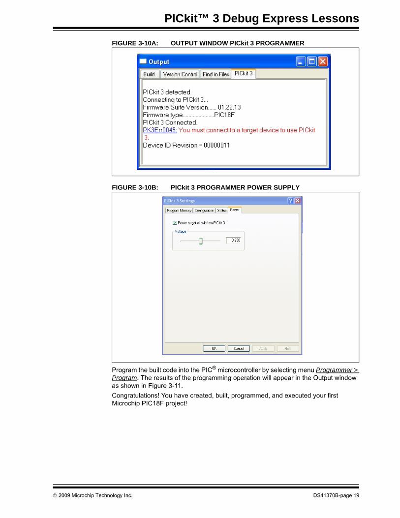
To program the code into the PIC18F45K20 microcontroller, the PICkit 3 Programmer/Debugger is used. Select the PICkit 3 as a programmer in the MPLAB IDE with Programmer > Select Programmer > 4 PICkit 3.This will create a new tab in the Output window for the PICkit 3 programmer, where messages from the programmer are displayed. The PICkit 3 will be initialized and should report finding the PIC18F45K20 microcontroller on the demo board as shown in Figure 3-10A.The PICkit 3 must be configured to supply power to the demo board, if not, the PICkit 3 will not see the target (as evidenced by the error message in Figure 3-10A). Use Programmer > Settings... to display the window appearing shown in Figure 3-10B. Navigate to the Power tab and use the slider bar to set the output voltage to 3.25V, check the box labeled “Power target circuit from PICkit 3” and press the OK button. Once power to the target is enabled, the device ID of the PIC18F45K20 will be displayed (last line in Figure 3-10A).
Note: If an error that the include file p18f45k20.h cannot be found is generated, this usually means that MPLAB C was installed without checking the Add header file path to MCC_INCLUDE environment variable option during setup. It is recommended to re-install MPLAB C with this option checked.
DS41370B-page 18 © 2009 Microchip Technology Inc.
PICkit™ 3 Debug Express Lessons
FIGURE 3-10A: OUTPUT WINDOW PICkit 3 PROGRAMMER
FIGURE 3-10B: PICkit 3 PROGRAMMER POWER SUPPLY
Program the built code into the PIC® microcontroller by selecting menu Programmer > Program. The results of the programming operation will appear in the Output window as shown in Figure 3-11.Congratulations! You have created, built, programmed, and executed your first Microchip PIC18F project!
© 2009 Microchip Technology Inc. DS41370B-page 19

PICkit™ 3 Debug Express
FIGURE 3-11: OUTPUT WINDOW PICkit 3 PROGRAMMING RESULTS
Note: If an error occurs during programming, consult the PICkit 3 help file in the MPLAB IDE. Select Help > Topics… then under the “Programmers” head-ing select “PICki t 3 Programmer” and click OK. On the Contents tab, select the “Troubleshooting” section for information.
DS41370B-page 20 © 2009 Microchip Technology Inc.

PICkit™ 3 Debug Express Lessons
3.2 LESSON 2: BLINK LEDThis lesson discusses the Configuration bits of the PIC18FXXXX microcontrollers and how to set them in an MPLAB C source file. It also presents using a library function and shows how delays can be used to blink an LED on the demo board.
3.2.1 Opening the Lesson 2 Project and Workspace in the MPLAB IDE
This and the remaining lessons already have a project and workspace defined. To open the workspace for Lesson 2, select menu File > Open Workspace… in the MPLAB IDE. Browse to the directory C:\Lessons\PICkit 3 Debug Express Lessons\02 Blink LED and open the 02 Blink LED.mcw file.Before opening the new workspace, the MPLAB IDE will prompt you to save the current workspace. It is generally a good idea to click Yes. Afterwards, the new workspace and project for Lesson 2 will open.
3.2.2 Defining Configuration Bit Settings in the Source CodeConfiguration bits are fuses in the PIC18FXXXX microcontrollers that are programmed along with the application code to set up or “configure” different microcontroller operating modes and enable or disable certain microcontroller features. For example, in the PIC18F45K20 the Configuration bits select such features as which oscillator option to use, whether the processor runs in Traditional or Extended mode; whether to use the Brown-out Reset circuit and which voltage to trip at; whether the Watchdog Timer is enabled or disabled and which options to use, and if the Flash memory code-protect feature is enabled, among many other options.Note that some features, such as the Watchdog Timer, can be configured so that it may be enabled or disabled by software in the Special Function Registers while the application code is executing. For detailed descriptions and information on the PIC18F45K20 Configuration bits, see Section 23.1 “Configuration Bits” in the data sheet, under the section heading 23.0 “Special Features of the CPU”.In the Lesson 2 source code, all Configuration bits are defined at the top of the 02 Blink LED.c file, as shown in Figure 3-12.
Key Concepts- Open existing project work spaces by selecting File > Open Workspace…
in the MPLAB IDE.- Configuration bits are special purpose fuse bits that set PIC microcontroller
modes of operation and enable or disable microcontroller features. - A number of libraries are included with the MPLAB C compiler with
predefined and compiled functions. The “MPLAB C18 C Compiler Libraries” document (DS51297) provides detailed information on all included libraries.
- Delays can be created to time events by using software loops.
© 2009 Microchip Technology Inc. DS41370B-page 21

PICkit™ 3 Debug Express
FIGURE 3-12: LESSON 2 “BLINK LED” CONFIGURATION BIT DEFINITIONS
The Configuration bits are defined using the #pragma config directive for each Configuration Word. The MPLAB C attributes used to reference each bit or bit field setting (i.e., “OSC = INTIO67”) may differ from one PIC18FXXXX microcontroller to another, depending on the features supported by a particular microcontroller. All the attributes available for a particular microcontroller may be found in the MPLAB IDE help. Let’s find the attributes for the PIC18F45K20:1. Select MPLAB IDE menu Help > Topics…In the “MPLAB Help Topics” dialog, find the “Language Tools” category and select the 2. “PIC18 Config Settings” topic as shown in Figure . Click OK.3. When the Help window opens, select the Contents tab, and expand the
“Configuration Settings” section.4. Select the PIC18F45K20 microcontroller to display all the Configuration bit set-
ting attributes that can be used with the #pragma config directive, as shown in Figure .
/** C O N F I G U R AT I O N B I T S ******************************/
#pragma config FOSC = INTIO67, FCMEN = OFF, IESO = OFF // CONFIG1H
#pragma config PWRT = OFF, BOREN = SBORDIS, BORV = 30 // CONFIG2L
#pragma config WDTEN = OFF, WDTPS = 32768 // CONFIG2H
#pragma config MCLRE = OFF,LPT1OSC = OFF, PBADEN = ON, CCP2MX = PORTC // CONFIG3H
#pragma config STVREN = ON, LVP = OFF, XINST = OFF // CONFIG4L
#pragma config CP0 = OFF, CP1 = OFF, CP2 = OFF, CP3 = OFF // CONFIG5L
#pragma config CPB = OFF, CPD = OFF // CONFIG5H
#pragma config WRT0 = OFF, WRT1 = OFF, WRT2 = OFF, WRT3 = OFF // CONFIG6L
#pragma config WRTB = OFF, WRTC = OFF, WRTD = OFF // CONFIG6H
#pragma config EBTR0 = OFF, EBTR1 = OFF, EBTR2 = OFF, EBTR3 = OFF // CONFIG7L
#pragma config EBTRB = OFF // CONFIG7H
FIGURE 3-13: MPLAB HELP TOPICS FIGURE 3-14: PIC18F45K20 CONFIGURATION
DS41370B-page 22 © 2009 Microchip Technology Inc.

PICkit™ 3 Debug Express Lessons
The Configuration bit settings that are important for this lesson project and are different from the default values are:
Even though all other bit settings are left as default, it is strongly recommended to define them all in the source as is done in the Lesson 2 source code. This ensures that the program memory image in the .hex file built by the compiler contains all the configuration settings intended for the target application. The one exception is the DEBUG bit, as this is defined by the MPLAB IDE environment depending on whether the target microcontroller is running in Debug mode or not.
3.2.3 Exploring the Lesson 2 Source CodeOpen the Lesson 2 source code file 02 Blink LED.c in an MPLAB IDE editor window if it is not open already.
FIGURE 3-15: LESSON 2 “BLINK LED” SOURCE CODE
This source code contains a couple of new lines of interest. The first is a new include file: #include "delays.h"
This is the header file for the MCC18 “delays” library, which provides functions used to create program delays of a certain number of processor cycles. The MPLAB C compiler comes with a number of useful libraries. These include the standard C libraries stdio and stdlib, and function libraries such as ctype, delays, math, and string. There are also libraries for using hardware peripheral functions such as adc, i2c, pwm, spi, usart, and timers as well as for software emulation of peripherals like sw_i2c, sw_uart, and sw_spi.
FOSC = INTIO67 This sets the PIC18F45K20 to run using the internal oscillator, so no crystal or external oscillator is needed. The default frequency is 1 MHz. The oscillator is covered in more detail in Lesson 9. It also sets OSC1 and OSC2 pins to be used as the RA6 and RA7 I/O port pins as the OSC pin functions are not needed.
WDTEN = OFF This turns off the Watchdog Timer, as it is not used in this lesson. When the Watchdog Timer is enabled, it must be cleared periodi-cally in the code or it will reset the microcontroller.
LVP = OFF This turns off Low-Voltage-Programming, and frees the PGM pin to be used as the RB5 I/O port pin. (LVP mode is not used by the PICkit 3 programmer.)
/** I N C L U D E S **************************************************/
#include "p18f45k20.h"
#include "delays.h"
/** D E C L A R A T I O N S *******************************************/
void main (void)
TRISD = 0b01111111;// PORTD bit 7 to output (0) ; bits 6:0 are inputs (1)
while (1)
LATDbits.LATD7 = ~LATDbits.LATD7; // toggle LATD
Delay1KTCYx(50);// Delay 50 x 1000 = 50,000 cycles; 200ms @ 1MHz
© 2009 Microchip Technology Inc. DS41370B-page 23
PICkit™ 3 Debug Express
Headers for the libraries can be found in the MCC18 header directory C:\MCC18\h. The source code for most of the libraries can be found in C:\MCC18\src, and the libraries themselves are in C:\MCC18\lib. For more detailed information on the included library functions see the “MPLAB C18 C Compiler Libraries” document (DS51297).The other new line of special interest is a function call to a function in the delays library: Delay1KTCYx(50);
This function creates a time delay with a software of 1000 (1k) instruction cycles (TCY) times the argument value. In this case, the argument is 50 so this function will delay for 50 x 1,000 = 50,000 instruction cycles. The instruction rate on PIC18FXXXX microcontrollers is equal to 1/4th the oscillator clock; in other words, it takes 4 clocks to execute an instruction. In this case the clock is the internal oscillator at 1 MHz, so the instruction rate is 250 kHz, or TCY = 4us per instruction. The total delay is 50,000 x 4us = 200 ms, which is slow enough for the human eye to see the LED turning on and off.The Lesson 2 program runs this delay inside an indefinite while loop, which sets the RD7 I/O pin to the complement of its current value (the effect is to switch it back and forth between high and low) with a 200 ms delay in between each RD7 output level change. This blinks the demo board LED 7.
3.2.4 Build and Program the Lesson 2 CodeSelect MPLAB IDE menu, build the Lesson 2 project and program the code into the demo board PIC18F45K20 using the PICkit 3 Programmer as we did in Lesson 1. The demo board LED 7 will blink continuously at 200 ms on and 200 ms off.
DS41370B-page 24 © 2009 Microchip Technology Inc.

PICkit™ 3 Debug Express Lessons
3.3 LESSON 3: ROTATE LEDThis lesson builds on the previous two lessons to introduce defining global variables and code sections, and to add rotation to the LED display. It will light up LED 0, then shift it to LED 1, then to LED 2 and on up to LED 7, and back to LED 0.In this and following lessons, please open the lesson workspace in the MPLAB IDE upon starting the lesson.
3.3.1 Allocating File Register Memory In the source code file 03 Rotate LED.c for Lesson 3 the global variable, LED_Number, is declared as in Figure 3-16.
FIGURE 3-16: LESSON 3 GLOBAL VARIABLE DECLARATION
The directive #pragma udata is used prior to declaring the variable LED_Number to indicate to the compiler that the following declarations are data variables that should be placed in the PIC18FXXXX file registers. This differs from PC compilers where instructions and variables share the same memory space due to the Harvard architecture of the PIC18FXXXX as discussed in Section 2.1 of this document.There are two directives for use with #pragma when defining variables:
Data declarations can also be given a section name. The section name may be used with a Linker Script SECTION entry to place it in a particular area of memory. See Section 2.9 of the “MPLAB C18 C Compiler User’s Guide” (DS51288) for more information on using sections with Linker Scripts. Even without a Linker Script section, the #pragma udata directive may be used to specify the starting address of the data in the file registers. For example, to place LED_Number at the start of file register Bank 3 declare the udata section as:
#pragma udata mysection = 0x300 unsigned char
LED_Number; // 8-bit variable unsigned int
AnotherVariable;
Other variables declared in a udata or idata section will be placed at subsequent addresses. For instance, the 16-bit integer AnotherVariable above would occupy address 0x301 and 0x302.Note that function local variables will be placed on the software stack.
Key Concepts- The directives #pragma udata and #pragma idata are used to allocate
memory for static variables in the file registers. - The directive #pragma code is used to indicate a section of instructions to
be compiled into the program memory of the PIC18FXXXX. - The directive #pragma romdata is used for constant (read-only) data
stored in the program memory. This is used with the keyword rom. - Constant data can be stored in program memory so as not to use up file
register RAM.
udata Uninitialized data. The following data is stored uninitialized in the file register space.
idata Initialized data. The following data is stored in the file register space. The initial-ization values are stored in program memory, and then moved by the start-up initialization code into file registers before program execution begins.
/** V A R I A B L E S *************************************************/
#pragma udata // declare statically allocated uninitialized variables
unsigned char LED_Number; // 8-bit variable
© 2009 Microchip Technology Inc. DS41370B-page 25

PICkit™ 3 Debug Express
For a list of data types supported by MPLAB C, their sizes and limits, see Section 2.1 of the “MPLAB C18 C Compiler User’s Guide” (DS51288).
3.3.2 Allocating Program MemoryProgram memory will most often be used for program instructions and constant data. The source code for Lesson 3 includes examples of both, as shown in Figure 3-17.
FIGURE 3-17: LESSON 3 CONSTANT DATA AND PROGRAM CODE
There are two basic directives for defining program memory sections:
In this lesson, we use a constant array LED_LookupTable to convert a number representing LEDs 0-7 to a bit pattern for setting the appropriate PORTD pin to turn on the corresponding LED. This constant is declared in a romdata section and uses the rom keyword so it will be placed in program memory. As the program never needs to change these array values, this saves file registers to be used for true variables.Note that the romdata section was also declared with a section name and absolute address:#pragma romdata Lesson3_Table = 0x180
These optional attributes will force the compiler to place the 8 – byte char array at program memory address 0x0180. If an address is not specified, the code or romdata section may not always be placed at a deterministic address by the linker.Select MPLAB IDE menu Project > Build All to build the Lesson 3 code, then select View > Program Memory to display the compiled contents of program memory. The instructions to execute the lesson program code are contained within addresses 0x0000 and 0x0146. Note that the array values have been compiled to program memory starting at the specified address of 0x180 through address 0x186 as shown in Figure 3-18.
code Program memory Instructions. Compiles all subsequent instructions into the program memory space of the target PIC18FXXXX.
romdata Data stored in program memory. Used in conjunction with the rom keyword, the following constant data is compiled into the program memory space.
/** D E C L A R A T I O N S *******************************************/
// declare constant data in program memory starting at address 0x180
#pragma romdata Lesson3_Table = 0x180
const rom unsigned char LED_LookupTable[8] = 0x01, 0x02, 0x04, 0x08,
0x10, 0x20, 0x40, 0x80;
#pragma code// declare executable instructions
void main (void)
DS41370B-page 26 © 2009 Microchip Technology Inc.

PICkit™ 3 Debug Express Lessons
FIGURE 3-18: PROGRAM MEMORY “LED_LOOKUPTABLE” ARRAY VALUES
The directive #pragma code is then used to specify the following section, beginning with the main () declaration, will be executable instructions to place in program memory. Since an optional section name and address are not specified, the code instructions will be placed at the first available address by the linker. As with data directives, a section name may be used with a SECTION entry in the Linker Script to allocate a range of program memory for a section.
3.3.3 Exploring the Lesson 3 Source CodeOpen the lesson source code file 03 Rotate LED.c in an editor window if it is not open already.
© 2009 Microchip Technology Inc. DS41370B-page 27

PICkit™ 3 Debug Express
FIGURE 3-19: LESSON 3 “ROTATE LED” SOURCE CODE
Here is the basic flow of our Rotate LED program:
3.3.4 Build and Program the Lesson 3 CodeIn the MPLAB IDE, build the Lesson 3 project and program the code into the demo board using the PICkit 3 Programmer. The demo board LEDs will rotate from LED 0 up to LED 7 and then back to LED 0.
/** V A R I A B L E S *************************************************/
#pragma udata // declare statically allocated uninitialized variables
unsigned char LED_Number; // 8-bit variable
/** D E C L A R A T I O N S *******************************************/
// declare constant data in program memory starting at address 0x180
#pragma romdata Lesson3_Table = 0x180
const rom unsigned char LED_LookupTable[8] = 0x01, 0x02, 0x04, 0x08,
0x10, 0x20, 0x40, 0x80;
#pragma code// declare executable instructions
void main (void)
LED_Number = 0;// initialize
TRISD = 0b00000000;// PORTD bits 7:0 are all outputs (0)
while (1)
// use lookup table to output one LED on based on LED_Number value
LATD = LED_LookupTable[LED_Number];
LED_Number++;// rotate display by 1
if (LED_Number == 8)
LED_Number = 0;// go back to LED 0.
Delay1KTCYx(50);// Delay 50 x 1000 = 50,000 cycles; 200ms @ 1MHz
Initialize Variables and I/O PortThe global variable LED_Number, which holds the number of the LED we cur-rently want on, is set to ‘0’ for the first LED.The TRISD register bits are all set to ‘0’, so that all 8 port D pins RD0-RD7 are outputs.
Loop Forever with the while(1) statement:Set the I/O Port to turn on an LED.
The number of the LED to turn on, LED_Number, is used an index to the array LED_LookupTable which returns a value with a bit set corresponding to the LED to be turned on. This value is written to the LATD register to turn on the one LED.
Rotate the LED numberThe LED number is incremented to the next LED. The if state-ment checks to see if it has been incremented past the last LED. If so, it is reset to the first LED, number 0.
Delay 200ms
As in Lesson 2, a “delays” library function is used to create a time delay.
(Loop End)
DS41370B-page 28 © 2009 Microchip Technology Inc.

PICkit™ 3 Debug Express Lessons
3.4 LESSON 4: SWITCH INPUTThe demo board switch is used in the lesson to rotate the LEDs once on each press.
3.4.1 Files and the #define Directive This lesson has added a header file to the project named 04 Switch Input.h as shown in Figure 3-20.
FIGURE 3-20: HEADER FILE
While it is assumed that the reader is familiar with C language header files, we’ll note that in the 04 Switch Input.h header file the #define directive has been used to give more meaningful names to the switch I/O pin variable and a constant value.
As with other C compilers use of #define, MPLAB C will replace all instances of the text “Switch_Pin” with the text “PORTBbits.RB0” at compile time. Remember, for the compiler to know about the #define definitions, the header file must be included in the C file, as is done in 04 Switch Input.c: #include "04 Switch Input.h" // header file
Key Concepts- The directive #define can be used to give SFR registers and bits more
meaningful names. - I/O pins that share an analog input channel must be configured as digital
pins if used as digital inputs using SFR ADCON1, or they will always read ‘0’.
- The PORTx SFRs are used to read the logic state on an input port pin. - Mechanical switch debouncing can be handled in software to eliminate
external components that may be otherwise required.
#define Switch_Pin PORTBbits.RB0#define DetectsInARow 5
© 2009 Microchip Technology Inc. DS41370B-page 29

PICkit™ 3 Debug Express
3.4.2 Switch Debouncing
Mechanical switches are frequently encountered in embedded processor applications, and are inexpensive, simple and reliable. However, such switches are also often very electrically noisy. This noise is known as switch bounce, whereby the connection between the switch contacts makes and breaks several, perhaps even hundreds, of times before settling to the final switch state. This can cause a single switch push to be detected as several distinct switch pushes by a fast device, especially with an edge- sensitive input. Think of advancing the TV channel, but instead of getting the next channel, the selection skips ahead two or three.Classic solutions to switch bounce involved filtering out the fast switch bounce transitions with a resistor-capacitor circuit, or using re-settable logic shift registers. While effective, these methods add additional cost and increase circuit board real estate. Debouncing a switch in software eliminates these issues.A simple way to debounce a switch is to sample the switch until the signal is stable. How long to sample requires some investigation of the switch characteristics, but usually 5ms is sufficiently long.This lesson code demonstrates sampling the switch input every 1mS, waiting for 5 consecutive samples of the same value before determining that the switch was pressed. Note that the switch on the 44-Pin Demo Board doesn’t bounce much, but it is good practice to debounce all system switches.
FIGURE 3-21: SWITCH DEBOUNCING PROGRAM FLOW
3.4.3 Exploring the Lesson 4 Source CodeOpen the lesson source code file 04 Switch Input.c in an editor window if it is not open already.
DS41370B-page 30 © 2009 Microchip Technology Inc.
PICkit™ 3 Debug Express Lessons
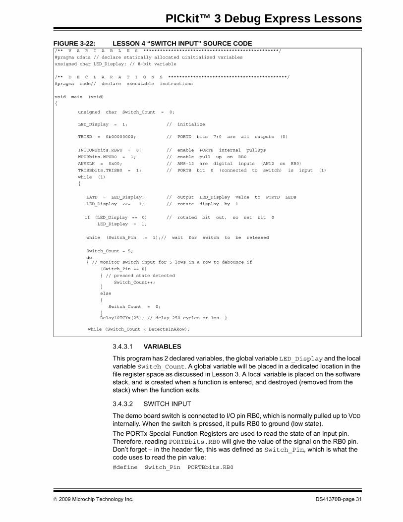
FIGURE 3-22: LESSON 4 “SWITCH INPUT” SOURCE CODE
3.4.3.1 VARIABLES
This program has 2 declared variables, the global variable LED_Display and the local variable Switch_Count. A global variable will be placed in a dedicated location in the file register space as discussed in Lesson 3. A local variable is placed on the software stack, and is created when a function is entered, and destroyed (removed from the stack) when the function exits.
3.4.3.2 SWITCH INPUT
The demo board switch is connected to I/O pin RB0, which is normally pulled up to VDD internally. When the switch is pressed, it pulls RB0 to ground (low state).The PORTx Special Function Registers are used to read the state of an input pin. Therefore, reading PORTBbits.RB0 will give the value of the signal on the RB0 pin. Don’t forget – in the header file, this was defined as Switch_Pin, which is what the code uses to read the pin value:#define Switch_Pin PORTBbits.RB0
/** V A R I A B L E S *************************************************/
#pragma udata // declare statically allocated uinitialized variables
unsigned char LED_Display; // 8-bit variable
/** D E C L A R A T I O N S *******************************************/
#pragma code// declare executable instructions
void main (void)
while (Switch_Count < DetectsInARow);
unsigned char Switch_Count = 0;
LED_Display = 1; // initialize
TRISD = 0b00000000; // PORTD bits 7:0 are all outputs (0)
INTCON2bits.RBPU = 0; // enable PORTB internal pullups
WPUBbits.WPUB0 = 1; // enable pull up on RB0
ANSELH = 0x00; // AN8-12 are digital inputs (AN12 on RB0)
TRISBbits.TRISB0 = 1; // PORTB bit 0 (connected to switch) is input (1)
while (1)
LATD = LED_Display; // output LED_Display value to PORTD LEDs
LED_Display <<= 1; // rotate display by 1
if (LED_Display == 0)
LED_Display = 1;
// rotated bit out, so set bit 0
while (Switch_Pin != 1);// wait for switch to be released
Switch_Count = 5;
do // monitor switch input for 5 lows in a row to debounce if
(Switch_Pin == 0)
// pressed state detected
Switch_Count++;
else
Switch_Count = 0;
Delay10TCYx(25); // delay 250 cycles or 1ms.
© 2009 Microchip Technology Inc. DS41370B-page 31

PICkit™ 3 Debug Express
In the PIC18F45K20, the RB0 pin is shared with analog input AN12. Such pins must be configured as either digital or analog inputs. This is important because RB0 will be used as a digital input pin to read the state of the switch in register PORTB. If RB0 is configured as an analog input, it will always read ‘0’ and not the actual state of the switch. Pins are configured as analog or digital in the SFRs ANSEL and ANSELH.
FIGURE 3-23: ANSELH: ANALOG REGISTER 1
We clear ANSELH to set all pins to digital functionality: ANSELH = 0x00;Now we can use RB0 as a digital input, so the TRISB bit is set to configure it as an input: TRISBbits.TRISB0 = 1;
3.4.3.3 ROTATING THE LEDS
This program uses a simpler method of rotating the LEDs than Lesson 3, which used the look-up table for demonstration purposes. 04 Switch Input.c uses a single set bit in the LED_Display variable which is written to LATD and shifted each time the display is updated. The bit will eventually be shifted out of the Most Significant bit of LED_Display, so the code checks for this, and sets LED_Display to ‘1’ again.For more information on I/O port pins, see Section 10 “I/O Ports” of the PIC18F45K20 Data Sheet (DS41303).
3.4.4 Build and Program the Lesson 4 CodeBuild the Lesson 4 project and program the code into the demo board using the PICkit 3 Programmer. Press the Demo Board Switch button to rotate the LEDs. The LEDs will advance once for each button press.
DS41370B-page 32 © 2009 Microchip Technology Inc.

PICkit™ 3 Debug Express Lessons
3.5 LESSON 5: USING TIMER0Timer0 is used to time delays while rotating the demo board LEDs, instead of using program loop delays. The demo board switch reverses the direction of the rotation.
3.5.1 The PIC18F45K20 Timer0 Module The Timer0 module is the timer/counter peripheral of the PIC18FXXXX microcontroller that may be used to count oscillator clock cycles or external events on the T0CKI pin. It can be configured as an 8-bit or 16-bit timer, which means it can count from 0 to 255 or 0 to 65535. A bit flag is set when the counter rolls over from the maximum value back to zero.The Timer0 module also includes an optional prescaler, which may be configured to divide the timer clock source before it reaches the timer/counter itself. For example, with a 1:1 prescaler, the timer would increment once every instruction clock cycle. (Remember that the instruction clock cycle TCY is the FOSC oscillator clock/4.) With a 1:8 prescaler, the timer would increment once every eight clock cycles. The prescaler is cleared on every write to the timer.
FIGURE 3-24: SIMPLIFIED 16-BIT TIMER0 BLOCK DIAGRAM
When Timer0 is configured as a 16-bit timer, care must be taken when reading and writing the timer value. The lower byte of the timer is directly readable and writable as the SFR TMR0L. However, the high byte is not directly accessible. Instead, it is buffered through the SFR TMR0H. TMR0H is updated with the value of timer high byte when TMR0L is read. A write of TMR0L also writes the contents of TMR0H to the Timer0 high byte. This allows the entire 16-bit timer to be read or written at once.Therefore, to read the timer, always read TMR0L first, then TMR0H. To write the timer, always write TMR0H first then TMR0L.Timer0 operation is controlled by the T0CON SFR, shown in Figure 3-24.
Key Concepts- Timer0 is hardware counter implemented in the microcontroller that can
count clock cycles or external events. - Using a timer instead of processor delay loops frees up the processor to do
useful work instead of counting cycles. - A timer “prescaler” sets the number of clock cycles or events required to
increment the timer by 1, allowing it to be run faster or slower off the same frequency clock.
TCY (Fosc / 4)
or T0CKI Pin Prescaler TMR0L
TMR0H
TMR0 High Byte
INTCON TMR0IF Bit
Prescaler may be set to divide by 2, 4, 8, 16, 32, 64, 128, or 256.
Timer high byte is buffered into TMR0H on a read of TMR0L. TMR0H is written to timer high byte on TMR0L write.
Flag bit set when TMR0 overflows, and must be cleared in software.
© 2009 Microchip Technology Inc. DS41370B-page 33

PICkit™ 3 Debug Express
FIGURE 3-25: T0CON: TIMER0 CONTROL REGISTER
To use Timer0 to replace the software delay Delay1KTCYx(50), it should be set up so it overflows about every 200 to 300 ms. Let’s go over the T0CON bit settings to make this happen:T08BIT = 0
Timer0 is configured as a 16-bit timer/counter to illustrate the buffering of TMR0H.T0CS = 0
Timer0 runs off the internal instruction clock. At Fosc = 1MHz, the instruction clock is 250kHz.
T0SE = 0If Timer0 was running off the T0CKI pin, this bit would determine whether it incre-mented on the falling edge or rising edge of the T0CKI pin signal. Since we are running off the instruction clock, this bit is a “don’t care.” This means operation is not affected by either setting of this bit.
PSA = 1The timer will overflow in 65536 counts. At the instruction clock rate of 250 kHz, the timer overflow will occur every 65536 x (1 / 250,000) = 262ms. This is a time in the range we want, so the prescaler is not assigned to Timer0. It runs directly off the instruction clock.
DS41370B-page 34 © 2009 Microchip Technology Inc.

PICkit™ 3 Debug Express Lessons
T0PS2:T0PS0 = 000Since the prescaler is not assigned, these bits are “don’t care.”
And finally:TMR0ON = 0
This bit turns the timer on and off. It’s set to zero now as the timer will be turned on once it is has been set up.
To configure Timer0 with these settings, the binary value 0b0000100 is written to T0CON.The PIC18F45K20 has 3 other configurable timers: Timer1, Timer2 and Timer3. More information on all four timer modules can be found in the PIC18F45K20 Data Sheet (DS41303), Sections 11 through 14.
3.5.2 Exploring the Lesson 5 Source CodeOpen the lesson source code file 05 Timer.c and header file 05 Timer.h in editor windows if they are not open already.Note that in 05 Timer.h two custom enumerated variable types have been defined:typedef enum LEFT2RIGHT, RIGHT2LEFT
LEDDirections;
typedef enum FALSE, TRUE BOOL;
This allows us to declare variables using these types and initialize them in main():LEDDirections Direction = LEFT2RIGHT;
BOOL SwitchPressed = FALSE;
The Direction variable keeps track of which direction the LEDs are rotating in, and SwitchPressed remembers if the switch has been pressed or not, as the LED rotation direction should only be changed once when it is pressed.The following code before the while(1) loop sets up the Timer0 module as discussed previously.
Using the line numbers in the comments as references, let’s discuss the function of each line in setting up the timer.Line 1 clears the TMR0IF flag in the INTCON SFR. This bit flag is set whenever the timer overflows (rolls over), so the program will poll it to know when the LED rotation delay is up. However, the flag will not reset by hardware, it must be reset in software so the program makes sure it is clear before starting the timer.Line 2 loads the settings into T0CON to configure the timer as discuss previously in this lesson.Line 3 clears the TMR0H buffer. Remember that TMR0H only buffers the high byte of the timer. The ‘0’ value will not actually be written to the timer upper byte until TMR0L is written.Line 4 clears TMR0L, which also causes TMR0H to be written to the high byte of the timer. Thus, the entire 16-bit timer is loaded with the hex value 0x0000.
// Init Timer
INTCONbits.TMR0IF = 0; // line 1
T0CON = 0b00001000; // line 2
// T0CON = 0b00000001; (ignore commented line for now)
TMR0H = 0; // line 3
TMR0L = 0; // line 4
T0CONbits.TMR0ON = 1; // line 5
© 2009 Microchip Technology Inc. DS41370B-page 35

PICkit™ 3 Debug Express
Line 5 sets bit 7, TMR0ON, of the T0CON register to turn on the timer so it begins incrementing. Using one of the SFR unions to access bits, like T0CONbits.TMR0ON, can change bits without affecting the other bits.
In the while(1) loop, the LED_Display global variable is updated to rotate the ‘1’ bit based on the Direction variable value, and then LATD is updated.The do…while() loop then polls the switch looking for a switch press while it waits for the timer to overflow and set the TMR0IF flag bit. This is a simplistic example of how using a timer allows the microcontroller to do work while waiting on a time delay, instead of wasting processing time counting cycles in an instruction loop.Once the switch it pressed, the Direction variable value is reversed. Follow the if – else if logic flow in the do…while() loop to see how once the switch is pressed, the direction is reversed only once until it is released and pressed again.Lastly, once Timer0 overflows and sets the TMR0IF flag the do…while() loop is exited. TMR0IF is then cleared in the software program so the next timer overflow can be detected.
3.5.3 Build and Program the Lesson 5 CodeBuild and program the Lesson 5 project. The LEDs will rotate, and pressing the Demo Board button will reverse them.
3.5.4 Assigning the Timer0 PrescalerNow we’ll go back to that commented-out line of code in the Timer0 setup statements. Comment out the T0CON assignment statement, and un-comment the other statement so the Timer0 setup code looks like this:
INTCONbits.TMR0IF = 0;
//T0CON = 0b00001000;
T0CON = 0b00000001;
TMR0H = 0;
TMR0L = 0;
T0CONbits.TMR0ON = 1;
Take a look at what this changes:PSA = 0
The prescaler is now assigned to Timer0, and the values of T0PSx will set the prescaler clock divider ratio.
T0PS2:T0PS0 = 001This value sets the prescale value to 1:4, which means Timer0 will now increment once every 4 instruction cycles instead of once every instruction cycle. It now takes 4 times as long for it to count up to 65536 – just over 1 second!
Rebuild and reprogram the Lesson 5 project with change in the source code. The LEDs will rotate more slowly, 4 times slower to be exact, than before.
Note: Be aware that some cases using an SFR union to access a bit may affect other bits. What actually happens during this instruction execution is the register is read, the bit is modified, and the entire register is re-written. This operation is called Read-Modify-Write. If a bit reads a different value than what it was last set as, this operation may affect register bits other than the intended one. Check the SFR bit definitions carefully. In the case of T0CON, all bits are Read/Write and all are set by software only; the hard-ware will not affect any bit setting.
DS41370B-page 36 © 2009 Microchip Technology Inc.

PICkit™ 3 Debug Express Lessons
3.6 LESSON 6: USING PICkit 3 DEBUG EXPRESSThis lesson covers using the PICkit 3 as an In-Circuit-Debugger (ICD). It uses the same MPLAB IDE workspace and project as Lesson 5. Set T0CON assignment back to the “no prescale” statement if it was changed in the last lesson.
3.6.1 Resources Reserved by the PICkit 3 Debug ExpressThe PICkit 3 Debug Express uses some on-chip resources to enable debugging. The resources are not available to the user application code.
3.6.1.1 GENERAL RESOURCES
• MCLR pin reserved for debugging; this pin cannot be used as digital I/O while debugging.
• The PGD and PGC port pins are reserved for programming and in-circuit debug-ging. Therefore, other functions multiplexed on these pins will not be available during debug.
• One stack level is used by the debugger and not available.
3.6.1.2 PROGRAM AND DATA MEMORY RESOURCES
The PICkit™ 3 Debug Express uses program memory and file register locations in the target device during debugging. These locations are not available for use by user code. In the MPLAB IDE, registers marked with an “R” in register displays represent reserved registers, as shown in Figure 3-26.
FIGURE 3-26: RESERVED ICD FILE REGISTER LOCATIONS IN THE PIC18F45K20
Key Concepts- An In-Circuit-Debugger like PICkit 3 uses some on-chip resources to enable
debugging. These reserved file registers and program memory locations are marked ‘R’ in the MPLAB IDE views, and are not available for use by the user application.
- Debugging also reserves one level of the hardware return address stack and two I/O pins.
- Debugging allows the program to be run, halted, stepped-through statement by statement, and for breakpoints to be set on program statements.
- The number of available breakpoints depends on the PIC microcontroller being used.
Note: This lesson uses the project and source code from Lesson 5: Using Timer0.
© 2009 Microchip Technology Inc. DS41370B-page 37

PICkit™ 3 Debug Express
3.6.2 Selecting PICkit 3 as a Debugger in the MPLAB IDEThe PICkit 3 cannot be used as a programmer and debugger at the same time, so if PICkit 3 is currently selected as a programmer, selecting it as a debugger will cause it to be disabled as a programmer.To enable the PICkit 3 as a debugger in the MPLAB IDE select Debugger > Select Tool > 2 PICkit 3. The Output window will display the connection to the target microcontroller as in Figure 3-10A.To Begin Debugging• In the MPLAD IDE toolbar, change the project configuration from “Rlease” to
“Debug”.• Build the project: Project > Build All • Program the target microcontroller: Debugger > Program• Select Debugger > Run to begin program execution. The Lesson 5 code is now running in Debug mode. The LEDs will rotate and the button may be pressed to reverse them, as the target microcontroller will operate in Debug mode just as it normally would.
3.6.3 Basic Debug Operations
3.6.3.1 HALT
The PIC18F45K20 on the demo board is now running the lesson program code. Code execution can be halted (stopped) at any time by selecting Debugger > Halt <F5>. A green arrow on the left margin of the MPLAB IDE editor window will show the next statement to be executed. Your code will probably have stopped in a different place than that shown in Figure 3-27.
FIGURE 3-27: GREEN ARROW POINTS TO NEXT STATEMENT TO EXECUTE
Note: An ICD ‘i’ Linker Script must be used when debugging, as discussed in Section 3.1.1 of this document. The lesson projects already use the correct Linker Script, 18f45k20 i.lkr.
DS41370B-page 38 © 2009 Microchip Technology Inc.

PICkit™ 3 Debug Express Lessons
3.6.3.2 STEP
Stepping, also known as single-stepping, allows the code to be executed one statement at a time. There are three step options:
Step IntoThis will step through statements one at a time until a function call is reached. When Step Into is selected on a function call, the debugger will step to the first statement in the called function. Shortcut key is <F7>.
FIGURE 3-28: STEP INTO
Step OverThis will step through statements one at a time. When a statement includes a function call, the entire function will execute and the debugger will step to the next statement after the function call. It will not step into the function. Shortcut key is <F8>.
FIGURE 3-29: STEP OVER
Step OutThis completes execution of the current function and steps to the next statement after the function call.
You can step through lesson code by using the shortcut key for Debugger > Step Over, <F8>.
3.6.3.3 RUN
Debugger > Run <F9> will begin code execution until it is halted by the user or encounters a breakpoint.
3.6.3.4 RESET
Debugger > Reset > Processor Reset will perform a full reset of the target microcontroller, so execution can begin again from the start of the program code. This is only available when the target is halted.Halt the demo board PIC18F45K20 if it is currently running, and select Debugger > Reset > Processor Reset <F6> This will open up a new file in the MPLAB IDE called c018i.c. This is the start-up code, part of the MPLAB C library. This library code initializes the C software stack, assigns appropriate data values to any initialized data variables, and jumps to the start of the application function main().
© 2009 Microchip Technology Inc. DS41370B-page 39

PICkit™ 3 Debug Express
FIGURE 3-30: C018 START-UP LIBRARY CODE
3.6.4 Using BreakpointsWhen debugging code, a “breakpoint” can be added to a program statement. When running the program, the debugger will halt the target upon reaching the breakpoint statement.In the MPLAB IDE 05 Timer.c source code, place the editor cursor on line 111, SwitchPressed = TRUE;, and right-click to open the contextual menu. Select Set Breakpoint as shown in Figure 3-31. A red octagon with the letter ‘B’ will appear in the editor margin to indicate a breakpoint has been set on that line.
DS41370B-page 40 © 2009 Microchip Technology Inc.

PICkit™ 3 Debug Express Lessons
FIGURE 3-31: SET BREAKPOINT ON LINE 111
FIGURE 3-32: BREAKPOINT SET
The statement we’ve placed the breakpoint on will be executed when the Demo Board Switch button is pressed. Select Debugger > Run to begin program execution. The demo board LEDs will rotate as the code runs since the breakpoint statement has not been executed yet.Press the Demo Board Switch button. The program will halt on the breakpoint statement, as shown in Figure 3-33. <F8> can now be used to step through the code.
© 2009 Microchip Technology Inc. DS41370B-page 41

PICkit™ 3 Debug Express
FIGURE 3-33: BREAKPOINT HALT
The number of breakpoints that can be set at once in a program depends on the PIC18FXXXX device being debugged. Select menu Debugger > Breakpoints… This will open a dialogue box to show the currently set breakpoints. The Silicon Debug Resource Toolbar provides information on the total number of breakpoints available for the selected device (“HW BP”) and the number of used breakpoints (“Used”). The PIC18F45K20 can have up to 3 breakpoints set at once, and has 2 currently available since one is already set on line 111 of 05 Timer.c.
FIGURE 3-34: BREAKPOINTS DIALOGUE
DS41370B-page 42 © 2009 Microchip Technology Inc.

PICkit™ 3 Debug Express Lessons
3.6.5 Watching Variables and Special Function RegistersAll the values in the file registers can be seen by opening View > File Registers, and the values in the Special Function Registers can be seen by opening View > Special Function Registers. However, keeping these windows open is not recommended. This is because the entire file memory and all SFRs must be read from the target device whenever it is Run, Halted, and on each Step. Reading all of this data over the ICD bus can take a significant amount of time. The actual time it takes depends on how much memory the target PIC18FXXXX has, and how fast the target oscillator is. The slower the target oscillator, the longer it will take as the oscillator speed directly affects the ICD bus speed.If you have opened either of these windows, please close them now.The best way to watch variables and SFRs is to use a Watch window. This way, only the variables and registers that are of interest are updated. To open a Watch window, select View > Watch.
FIGURE 3-35: WATCH WINDOW
SFRs may be added to the Watch window by selecting them in the dropdown box on the upper left, and clicking the Add SFR button. Go ahead and add PORTB, which is used to read the switch state, and LATD, which our program uses to set the LEDs.User variables are added using the dropdown on the upper right, and clicking the Add Symbol button.Add the LED_Display, SwitchPressed, and Direction variables now.
Note: The number of active breakpoints can affect using the Step Into and Step Over functions. When these functions are used, a breakpoint is set at the next statement to step to. If all breakpoints are currently used and none are available, the MPLAB IDE is not able to set a breakpoint on the next C statement. Instead, it must step through each assembly instruction until the next statement is reached. If using Step Over, it may take some time to step over all the assembly functions in the compiled function. Free up a breakpoint to avoid this issue.
© 2009 Microchip Technology Inc. DS41370B-page 43

PICkit™ 3 Debug Express
FIGURE 3-36: WATCH VARIABLES
For each watch variable, the Watch window displays the File Register Address, the Symbol Name (variable name), and current Value. The value display format can be changed by right-clicking on a value and selecting Properties from the pop-up menu. Note that our two enumerated type variables, SwitchPressed and Direction will display the enumeration value, and not the mnemonic.The Watch window can also be used to edit variable values. Select the LATD value by clicking on it, and type in the hex value ‘AA’. Press enter to set the value. Look at the demo board; note that every other LED is now turned on. This is because through the Watch window, we just directly wrote to the LATD register the value 0xAA, which is binary 0b10101010!Select the PORTB symbol, right-click and select Properties. In the properties dialogue, go to the dropdown box for “Format:” and select “Binary”. Click OK to close the dialogue. The PORTB value is now displayed in a binary format, with bit 7 on the left.Step through the code once using <F8>. Note the value for PORTB bit 0, which is pin RB0 and connected to the demo board switch. The bit value should now be set (‘1’). While pressing down the Demo Board button, step again with <F8>. Note that PORTB bit 0 is now low since the switch is pressed!Take some time to play with the lesson code, stepping through it and watching variables and the demo board LEDs. You can also press the button and step through the switch detection statements. Set different breakpoints to experiment using them.Add TMR0L and TMR0H SFRs to the Watch window, and observe them counting while you step through the code. Note that they don’t increment once per step, as each C statement may be compiled into more than one assembly instruction and Timer0 is incremented once per assembly (machine) instruction.
Note: The “Value” fields in the Watch window, File Register window, and Special Function Register windows may not be valid immediately after first being opened. Step the code once to update the values.
DS41370B-page 44 © 2009 Microchip Technology Inc.
PICkit™ 3 Debug Express Lessons
3.7 LESSON 7: ANALOG-TO-DIGITAL CONVERTER (ADC)Lesson 7 builds on the previous lesson by using the on-chip ADC to read the demo board potentiometer voltage. The result is used to vary the LED rotation time delay so that the potentiometer controls the LED rotation speed.
3.7.1 PIC18F45K20 ADC Basics Simply put, an ADC takes the ratio of an input voltage to a reference voltage and represents it as a number. This number is dependent on the bits of resolution of the ADC. For example, the 10-bit resolution of the PIC18F45K20 ADC means that 1024 numbers from 0-1023 are available to represent the voltage ratio. In mathematical terms,ADC Value = (VIN/VREF) * 1023If VIN = 2.5Volts, and VREF = 5.0Volts, then the ADC Value is (2.5/5)*1023 = 511. This makes sense in that VIN is half of VREF, so the ADC value is half of 1023.Knowing the reference voltage and solving the equation for VIN allows the ADC Value to be converted back into a voltage:VIN = (ADC Value/1023) * VREF
The PIC18F45K20 ADC may be referenced to the device VDD voltage or an external voltage reference. In this lesson, the ADC is referenced to the PIC18F45K20 Starter Kit Demo Board VDD, which is supplied by PICkit 3. This voltage is typically around 3.3V for this device.The ADC can convert the voltage from any one of 13 channels on the PIC18F45K20. These analog input channels, numbered AN0 up to AN12, are shared with digital microcontroller pins and must be configured as analog inputs to be used with the ADC.The ADC is configured and controlled by 5 Special Function Registers: ANSEL, ANSELH, ADCON0, ADCON1 and ADCON2. These are covered in detail in the next section.
3.7.2 ADC Configuration and OperationLooking at the schematic of the 44-Pin Demo Board in the Appendix, the potentiometer (RP1) output is connected to the RA0/AN0 pin of the PIC18F45K20.The basic steps needed to convert the ADC voltage on this pin are:1. Configure the RA0/AN0 pin as an analog input in ANSEL. 2. Set the ADC voltage references in ADCON1. 3. Set the result justification, ADC clock source, and acquisition time in ADCON2. 4. Select the channel and turn on the ADC in ADCON0. 5. Start the conversion in ADCON0. #1: To use a pin as an analog input, it must not be used by other peripheral functions multiplexed on the same pin. The pin TRIS bit must be set to ‘1’ (input) and the ANSEL bit associated with RA0 should be set to ‘1’ (analog input). However, we still want RB0/AN12 configured as a Digital input to for the switch. Therefore, we will clear ‘0’ the AN12 bit in ANSELH.
Key Concepts- An Analog-to-Digital Converter is used to convert an analog voltage level
into a digital number representing the voltage. - The ANSEL, ANSELH, ADCON0, ADCON1, and ADCON2 SRFs configure
and control the on-chip ADC. - A timer register can be written to a value that will cause a timer overflow at a
specific time interval required by the application.
© 2009 Microchip Technology Inc. DS41370B-page 45

PICkit™ 3 Debug Express
#2: The VCFGx bits in ADCON1 can select the ADC voltage references to use the AN2 and AN3 pins, VDD and VSS, or some combination. Since the demo board does not have voltage references connected to AN2 and AN3, the ADC will be referenced to VDD and VSS. This means an ADC result of ‘0’ corresponds to 0 Volts, or VSS. A result of ‘1023’ corresponds to about 3.3 Volts, or VDD. Including the values from #1, the ADCON1 setting for this lesson isADCON1 = 0;
FIGURE 3-37: ADCON2: A/D CONTROL REGISTER 2
#3: The ADC clock should be set as short as possible but still greater than the minimum period “TAD” time, data sheet parameter 130. The minimum TAD time for the PIC18F45K20 (as of this writing) is1.4us. At a 1 MHz oscillator FOSC, selecting bits ADCS = FOSC/2 gives a 500 kHz ADC clock. One clock period 1/500kHz = 2us, which is greater than the minimum TAD = 1.4us. Thus ADCSx = ‘000’.
DS41370B-page 46 © 2009 Microchip Technology Inc.

PICkit™ 3 Debug Express Lessons
The ACTQx bits determine the acquisition time, and should take into account the internal acquisition time Tacq of the ADC, data sheet parameter 132, and the settling time of the application circuit connected to the ADC pin. From the data sheet, the internal acquisition time Tacq = 1.4us over temperature. The application circuit is an RC network formed by the potentiometer and capacitor C3, which has a very long settling time. For this demo lesson, we’ll simply set ACQTx to the largest value, 20TAD or ‘111’. 20 TAD is 20 times the ADC Clock period, or 20 * 2us = 40us.For result justification, we choose bit ADFM = 0 to the result is left-justified. This makes it easy to get the 8 Most Significant bits of the result from ADRESH. Thus the ADCON2 configuration value is:ADCON2 = 0b00111000#4: The demo board potentiometer is connected to AN0, so Channel 0 is selected in ADCON0. Bit ADON is set to ‘1’ to turn on the ADC peripheral. The GO/DONE bit is left clear as we don’t wish to start a conversion yet.ADCON0 = 0b00000001
FIGURE 3-38: ADCON0: A/D CONTROL REGISTER 0
© 2009 Microchip Technology Inc. DS41370B-page 47

PICkit™ 3 Debug Express
#5: To begin an ADC conversion, set bit 1 of ADCON0, the GO/DONE bit. When the conversion is done the hardware will clear that bit, so the GO/DONE may then be polled to wait for the conversion to complete. Once the conversion is complete and GO/DONE = 0, the ADC conversion result may be read from ADRESH and ADRESL.
3.7.3 Exploring the Lesson 7 Source Code
Open the lesson source files 07 ADC.c and 07 ADC.h in an MPLAB editor window if they are not already open.Of note is that the Timer0 setup code has been moved into a function and replaced with a function call. Two new functions were added to support the ADC.void Timer0_Init(void)
void ADC_Init(void) unsigned char
ADC_Convert(void)
The function prototypes have also been added to the header file, 07 ADC.h.In main() before getting to the while(1) loop, the program makes two function calls to set up the Timer0 and ADC peripherals using Timer0_Init() and ADC_Init(), respectively.To change the LED rotation speed based on the potentiometer, the ADC conversion value is used to set Timer0 just after it overflows. The higher the value written to Timer0, the less time it takes to overflow again, as the timer counts up from the written value. This is accomplished with two new statements at the bottom of the while(1) loop:
The TMR0H buffer is written with the 8 Most Significant bits of the ADC conversion, and then is written with Timer0 with a ‘0’ in the low byte on the TMR0L assignment statement. Recall from Lesson 5 that since TMR0H is actually a buffer and not the upper byte of the timer, and is written to the timer when TMR0L is written. Thus, it must be written first as it is here.We can calculate the amount of delay for a given ADC value, knowing that Timer0_Init() sets the TMR0 prescaler to 1:4, and our oscillator is 1MHz. Timer0 will count at 4 * the instruction rate, or 4 * 1/(FOSC/4) = 4 * 1/(1MHz/4) = 4 * 1/250kHz = 16 us. The number of counts until overflow occurs is 0x10000 – (start count) where (start count) is the value written to TMR0 – The ADC result in the upper byte and 0x00 in the lower. The total delay is then the number of counts times the count rate. For an ADC result of 0x81, the delay is (0x10000 – 0x8100) * 16 us = 0x7F00 * 16 us = 32512 * 16 us = 0.52 seconds.
3.7.4 Build and Run the Lesson 7 Code with PICkit 3 Debug ExpressBuild and program the Lesson 7 project, then Run the application in the debugger. Turning the demo board potentiometer will affect the rotation speed of the LEDs. The switch may be pressed to reverse the rotation.Halt the Lesson 7 program. Note that several SFRs and variables have already been added to a Watch window. Use Breakpoints and Step commands to explore the code. Observe how the ADC result in ADRESH is affected by the potentiometer voltage, and how this result is copied into TMR0.
TMR0H = ADC_Convert(); // MSB from ADCTMR0L = 0; // LSB = 0
DS41370B-page 48 © 2009 Microchip Technology Inc.

PICkit™ 3 Debug Express Lessons
See Section 19.0 “10-Bit Analog-to-Digital Converter (A/D) Module” in the PIC18F45K20 Data Sheet (DS41303) for more information on the ADC peripheral.
3.8 LESSON 8: INTERRUPTS
This lesson changes the Lesson 7 code to use interrupts to act on the switch press and Timer0 events instead of polling them. The switch uses the RB0/INT0 external interrupt capability.
3.8.1 PIC18FXXXX Interrupt Architecture When a peripheral requires attention or an event occurs, it sets an interrupt flag. Each flag has an interrupt enable bit that determines whether it will generate an interrupt to the microcontroller or not. In the previous lessons, interrupt flags such as TMR0IF were polled, but did not create an interrupt as the enable bit was not set. The enable bits allow only selected events to cause in interrupt. All interrupts are ORed together, and then ANDed with a global interrupt enable.
FIGURE 3-39: SIMPLIFIED INTERRUPT LOGIC
Note: If TMR0L is added to the Watch window, it will cause incorrect operation when stepping through the following 2 lines of code:
TMR0H = ADC_Convert();
TMR0L = 0;
This is caused by the buffered nature of TMR0H. When “Stepping Over” the TMR0H assignment statement, the MPLAB IDE will read the TMR0L register to update the value in the Watch window. When TMR0L is read, the upper byte of TMR0 is loaded into the TMR0H buffer, wiping out the value written in the previous TMR0H assignment statement.One workaround to be able to add TMR0L to the Watch window is to make sure not to step from the TMR0H to the TMR0L statement. Set a breakpoint on the TMR0L assignment statement, and Run from the TMR0H assignment statement.
Key Concepts- An interrupt is a hardware-based event that “interrupts” the program code to
execute a special function. When the interrupt function exits, program exe-cution returns to where it left off.
- The PIC18FXXXX supports a single interrupt priority or two levels of inter-rupt priority.
- A Low Priority interrupt can interrupt the main program. A High Priority inter-rupt can interrupt the main program or a low priority interrupt.
- The directives #pragma interruptlow and #pragma interrupt are used to define the interrupt functions.
© 2009 Microchip Technology Inc. DS41370B-page 49

PICkit™ 3 Debug Express
When an interrupt occurs and the Master Interrupt signal is asserted, the PIC microcontroller finishes executing the current instruction, stores the next address on the Return Address Stack, and then jumps to an interrupt vector. At the interrupt vector it begins executing a function designated as the Interrupt Service Routine. When this function exits, program execution returns to the address stored on the Return Address Stack.Interrupts allow hardware events to be acted upon very quickly and regardless of the state of the main program because they cause the immediate execution of dedicated code.The PIC18FXXXX architecture supports up to two levels of interrupt priority, each of which have a logic structure like that in Figure 3-37. Most interrupts have a Priority bit associated with the interrupt flag and enable that assigns it to one of the two priority levels. Using priority levels is optional, and the PIC18FXXXX may be configured to use only one level priority.When two levels of interrupt priority are used, an interrupt of either priority level may interrupt the main program. However, only a high priority interrupt may interrupt a low priority interrupt, and nothing may interrupt a high priority interrupt. As shown in Figure 3-38, when a low priority interrupt event occurs during execution of statement3 in the main code, the program jumps to begin executing the low priority interrupt function. During execution of the lo_statement2, a high priority interrupt event occurs, causing program execution to jump to the High Priority Interrupt function. When the high priority function completes and exits, execution is returned to where it left off in the low priority function. Similarly, when the low priority function completes and exits, program execution returns to where it left off in the main code, at statement4.
FIGURE 3-40: PRIORITY INTERRUPT EXECUTION FLOW
The high priority interrupt vector is at program memory address 0x0008. The low priority interrupt vector is at program memory address 0x0018. If interrupt priorities are not used, all interrupts jump to the high priority vector at 0x0008.
3.8.2 Exploring the Lesson 8 Source CodeThe first thing to note is that the Directions variable is now global, so it may be accessed in the Interrupt Service Routine functions.When using interrupts, the interrupt vectors must be defined and placed at the appropriate vector addresses using the #pragma code directives. An inline assembly GOTO statement redirects program execution to the interrupt functions, whose name serves as the GOTO argument.
DS41370B-page 50 © 2009 Microchip Technology Inc.

PICkit™ 3 Debug Express Lessons
FIGURE 3-41: DEFINE INTERRUPT VECTORS
The Interrupt Service Routine functions themselves are then declared with the #pragma interrupt directive for the high priority vector, and #pragma interruptlow for the low priority. Note the names must match between the vector GOTO argument, the #pragma attribute, and the function declaration name. The interrupt functions may call other functions defined elsewhere in the source, though the lesson source code does not do this.
FIGURE 3-42: INTERRUPT SERVICE FUNCTIONS
As all interrupts of the same priority vector to the same function, it is necessary in the function to examine which of the enabled interrupt flags caused the interrupt. Once the flag is found so that peripheral or event may be serviced, the software must clear the interrupt flag bit to reset the interrupt. In the lesson source code, the high priority interrupt routine looks for the INT0 pin interrupt INT0IF flag bit. Examples are shown in the source code of how it might check for other enabled interrupts, such as Timer1 TMR1IF and the ADC ADIF although neither of these interrupts are enabled in the lesson code. Similarly, the low priority vector checks for the Timer0 flag TMR0IF.Setting Up InterruptsNow that the source code has defined the interrupt vectors, and has functions to deal with the interrupts, it must properly setup and configure the interrupting logic and enable the individual interrupts it wants to use.Timer0 and external pin interrupts are set up using the INTCONx Special Function Registers. Other interrupts are setup through a number set of peripheral interrupt SFRs: PIRx, PIEx and IPRx. The PIRx registers contain the interrupt flags. The
/** I N T E R R U P T S ***********************************************/
//----------------------------------------------------------------------------// High priority interrupt vector
#pragma code InterruptVectorHigh = 0x08 void InterruptVectorHigh (void) _asm goto InterruptServiceHigh //jump to interrupt routine _endasm
//----------------------------------------------------------------------------// Low priority interrupt vector
#pragma code InterruptVectorLow = 0x18 void InterruptVectorLow (void) _asm goto InterruptServiceLow //jump to interrupt routine _endasm
// Iterrupt Service Routines#pragma interrupt InterruptServiceHigh// "interrupt" pragma for high priorityvoid InterruptServiceHigh(void) //function statements
// return from high-priority interrupt
#pragma interruptlow InterruptServiceLow // "interruptlow" pragma for low priorityvoid InterruptServiceLow(void) //function statements // return from low-priority interrupt
© 2009 Microchip Technology Inc. DS41370B-page 51
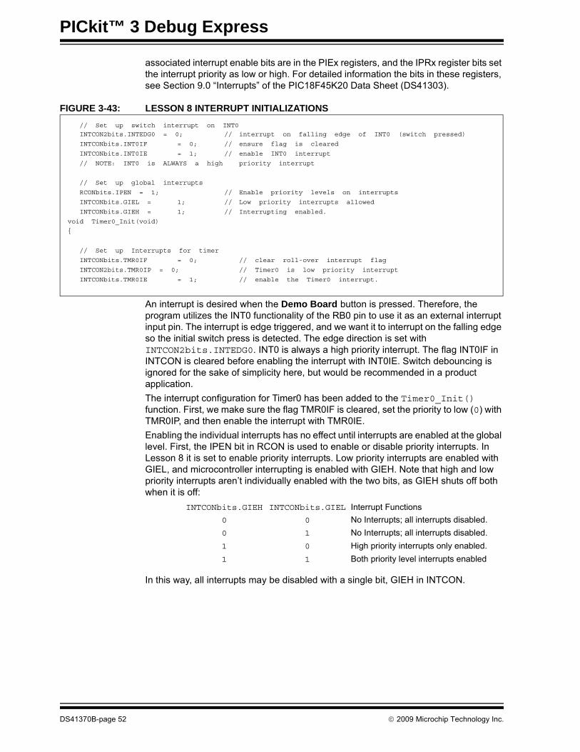
PICkit™ 3 Debug Express
associated interrupt enable bits are in the PIEx registers, and the IPRx register bits set the interrupt priority as low or high. For detailed information the bits in these registers, see Section 9.0 “Interrupts” of the PIC18F45K20 Data Sheet (DS41303).
FIGURE 3-43: LESSON 8 INTERRUPT INITIALIZATIONS
An interrupt is desired when the Demo Board button is pressed. Therefore, the program utilizes the INT0 functionality of the RB0 pin to use it as an external interrupt input pin. The interrupt is edge triggered, and we want it to interrupt on the falling edge so the initial switch press is detected. The edge direction is set with INTCON2bits.INTEDG0. INT0 is always a high priority interrupt. The flag INT0IF in INTCON is cleared before enabling the interrupt with INT0IE. Switch debouncing is ignored for the sake of simplicity here, but would be recommended in a product application.The interrupt configuration for Timer0 has been added to the Timer0_Init() function. First, we make sure the flag TMR0IF is cleared, set the priority to low (0) with TMR0IP, and then enable the interrupt with TMR0IE.Enabling the individual interrupts has no effect until interrupts are enabled at the global level. First, the IPEN bit in RCON is used to enable or disable priority interrupts. In Lesson 8 it is set to enable priority interrupts. Low priority interrupts are enabled with GIEL, and microcontroller interrupting is enabled with GIEH. Note that high and low priority interrupts aren’t individually enabled with the two bits, as GIEH shuts off both when it is off:
In this way, all interrupts may be disabled with a single bit, GIEH in INTCON.
// Set up switch interrupt on INT0
INTCON2bits.INTEDG0 = 0; // interrupt on falling edge of INT0 (switch pressed)
INTCONbits.INT0IF = 0; // ensure flag is cleared
INTCONbits.INT0IE = 1; // enable INT0 interrupt
// NOTE: INT0 is ALWAYS a high priority interrupt
// Set up global interrupts
RCONbits.IPEN = 1; // Enable priority levels on interrupts
INTCONbits.GIEL = 1; // Low priority interrupts allowed
INTCONbits.GIEH = 1; // Interrupting enabled.
void Timer0_Init(void)
// Set up Interrupts for timer
INTCONbits.TMR0IF = 0; // clear roll-over interrupt flag
INTCON2bits.TMR0IP = 0; // Timer0 is low priority interrupt
INTCONbits.TMR0IE = 1; // enable the Timer0 interrupt.
INTCONbits.GIEH INTCONbits.GIEL Interrupt Functions0 0 No Interrupts; all interrupts disabled.0 1 No Interrupts; all interrupts disabled.1 0 High priority interrupts only enabled.1 1 Both priority level interrupts enabled
DS41370B-page 52 © 2009 Microchip Technology Inc.

PICkit™ 3 Debug Express Lessons
FIGURE 3-44: LESSON 8 INTERRUPT SFRS
In the Lesson 8 source code, all the statements to change the rotation direction are in the INT0 switch interrupt function, and the statements to rotate the LED display are in the TMR0 interrupt function. All that remains in the main program is a while() loop that updates the PORTD register with LED_Display. This statement could have also been placed in the TMR0 interrupt function, but is left in the main program to illustrate how the main program runs continuously and interacts with the interrupts.Single Priority InterruptsIf only a single level of interrupts were used (RCON bit IPEN = 0), then it is only necessary to define the interrupt vector at 0x0008, and a single Interrupt Service Routine function with #pragma interrupt. All priority bit settings are ignored. The function of the INTCON bits GIEH and GIEL become GIE and PEIE, respectively, with the following functions:
3.8.3 Build and Run the Lesson 8 Code with PICkit 3 Debug ExpressBuild and program the Lesson 8 project, then Run the application in the debugger. Turning the demo board potentiometer will affect the rotation speed of the LEDs. The switch may be pressed to reverse the rotation. Use breakpoints to explore the interrupting functions.
INTCONbits.GIE INTCONbits.PEIE Interrupt Functions0 0 No Interrupts; all interrupts disabled.0 1 No Interrupts; all interrupts disabled.1 0 Only interrupts enabled in INTCONx
enabled.All PIEx interrupts remain disabled.
1 1 All interrupts, including those enabled in PIEx registers, are enabled.
© 2009 Microchip Technology Inc. DS41370B-page 53

PICkit™ 3 Debug Express
3.9 LESSON 9: INTERNAL OSCILLATORUsing the on-chip internal oscillator and PLL (Phase Locked Loop) of the PIC18F45K20 is discussed. Clocks from 31 kHz up to 64 MHz can be generated without requiring external oscillator components.
3.9.1 The Internal Oscillator Block The internal oscillator block of the PIC18F45K20 generates two different clock signals. The main output, INTOSC, is a factory calibrated 16 MHz clock source with postscaler that can provide a range of clock frequencies down to 31 kHz.The other output, INTRC, is a nominal 31 kHz clock source that drives peripherals such as the Power-up Timer, the Fail-Safe Clock Monitor, the Watchdog Timer and the Two-Speed Start-up feature.When the oscillator block is set to provide a 31 kHz clock to the microcontroller, it can be selected as a postscaled output of INTOSC, which has the benefit of calibrated accuracy, or INTRC, which has the benefit of lower power consumption.The oscillator block also contains a 4x PLL (Phase Locked Loop) frequency multiplier that can increase the microcontroller clock source up to 32 MHz. The PLL is only available when the internal oscillator block selected output is 8 MHz or 16 MHz. It will multiply the base 4 MHz signal by 4 to 32 MHz, and the 8 MHz base clock to 64 MHz.This allows the internal oscillator block to provide a range of 10 different software selectable frequencies of 31 kHz, 250 kHz, 500 kHz, 1 MHz, 2 MHz, 4MHz, 8 MHz, 16 MHz and (with the PLL) 32 MHz and 64 MHz. Recall from previous lessons that the default frequency on a Reset is 1 MHz.
FIGURE 3-45: SIMPLIFIED INTERNAL OSCILLATOR BLOCK DIAGRAM
Key Concepts- To use the internal oscillator block, set the OSC Configuration bits to
INTIO67 or INTIO7. The latter outputs the clock signal CLKO on the RA6 pin.
- The OSCCON Special Function Register is used to set the base internal oscillator frequency from 31 kHZ up to 16 MHz.
- The OSCTUNE register allows the internal oscillator frequency to be adjusted on a fine scale and enables or disables the PLL.
- The 4x PLL may only be used when base frequencies of 8 MHz or 16 MHz are selected in OSCCON. Enabling the PLL multiplies the base frequency by 4, providing clocks at 32 MHz and 64 MHz, respectively.
DS41370B-page 54 © 2009 Microchip Technology Inc.

PICkit™ 3 Debug Express Lessons
3.9.2 Configuring the Internal OscillatorThe internal oscillator block is selected as the primary oscillator in the Configuration bits. The OSC bits in the CONFIG1H Configuration Word are set to either INTIO67 or INTIO7. When INTIO67 is selected, the internal oscillator is the primary oscillator with the external oscillator pins OSC2 and OSC1 available as RA6 and RA7 IO. OSC = INTIO7 differs only in that RA6 is not available; instead the internal instruction clock is output as CLKO on that pin.The two Special Function Registers that control the internal oscillator block in software are OSCCON and OSCTUNE, shown in figures 3-44 and 3-45.
FIGURE 3-46: OSCCON: OSCILLATOR CONTROL REGISTER
The IDLEN bit in OSCCON affects how the oscillator behaves in power managed modes, and is not discussed further here.The IRFCx bits determine the internal oscillator frequency. These are the outputs of the postscaler. As Note 2 in Figure 3-44 indicates, the 31 kHz clock can be selected as either a postscaled version of the INTOSC 8 MHz oscillator, on which all other frequencies are based, or the INTRC low-power 31 kHz oscillator as discussed in Section 3.9.1. This selection is made with the INTSRC bit in the OSCTUNE register.
© 2009 Microchip Technology Inc. DS41370B-page 55

PICkit™ 3 Debug Express
The IRFCx bits may be changed by software during program execution, allowing the program to “throttle” the microcontroller execution speed to current processing needs. This can save on power consumption when fast clock speeds aren’t required.The OSTS and IOFS bits are read-only Status bits. The PIC18F45K20 has the option to start-up running off the internal oscillator until an external oscillator circuit has stabilized. This allows faster start-up of the microcontroller with external oscillators. OSTS is used to alert the software when the clock source has switched over to the external primary oscillator. This functionality is not covered further in this lesson. The SCSx bits allow the software to switch the microcontroller clock source over to the internal oscillator block even when an external oscillator has been selected in the Configuration bits. The secondary oscillator may also be selected, which is the low-speed low-power oscillator that is part of Timer1 and is usually run with a 32 kHz crystal for Real-Time Clock (RTC) applications. In this lesson, the internal oscillator has been selected as the primary oscillator in the Configuration bits, and SCS1:SCS0 = 00.
FIGURE 3-47: OSCTUNE: OSCILLATOR TUNING REGISTER
The 5 TUNx bits in OSCTUNE allow small adjustments in the INTOSC oscillator frequency. This can be used to calibrate the frequency more accurately than the factory calibration, and adjust for drift over VDD and temperature changes.The PLLEN bit enables the PLL, multiplying the INTOSC output by 4. Note that the PLL may only be enabled for INTOSC = 8 MHz or INTOSC = 16 MHz. Enabling the PLL with a 4 MHz base frequency gives a 16 MHz clock, and with a 16 MHz base frequency gives 64 MHz.For further information on the internal oscillator block, see Section 2.6 of the PIC18F45K20 Data Sheet (DS41303).
DS41370B-page 56 © 2009 Microchip Technology Inc.

PICkit™ 3 Debug Express Lessons
3.9.3 Exploring the Lesson 9 Source CodeThe Lesson 9 program code has a simple background loop in the main() function that displays a binary count on the demo board LEDs, as shown in Figure 3-46. Each count increment is delayed by 64,000 instruction cycles. As the clock frequency is changed, the instruction rate changes and so the total time in seconds of the delay gets shorter as the clock frequency increases. The effect is that the LED display will count faster as the clock speed is increased.At the start of the program, the internal oscillator is running at 250 kHz. Each press of the demo board switch creates an interrupt that increases the clock frequency by a factor of 2 up through 64 MHz, after which it returns to 250 kHz.
FIGURE 3-48: SOURCE CODE BACKGROUND LOOP
A few other things of interest in the Lesson 9 source code are:• The interrupts are configured for only a single level of priority, where interrupt pri-
orities are disabled. This differs from the Lesson 8 source code where interrupt priorities were enabled.
• Instead of using ADCON1 to configure the switch input RB0 as a digital input as was done in previous lessons, the Lesson 9 source sets the Configuration bit PBADEN = OFF. This causes all PORTB pins to default to digital, instead of ana-log, inputs on a Reset.
• The Lesson 9 interrupt service function void InterruptService(void) dem-onstrates calling another function void SetIntOSC(IntOSCFreq *ClockSet) from within the interrupt service code.
3.9.4 Build and Run the Lesson 9 Code with PICkit 3 Debug ExpressBuild and program the Lesson 9 project, then Run the application in the debugger. Pressing the demo board switch causes the program to change the oscillator frequency during execution. As the oscillator frequency increases, the rate at which the LEDs count increases.
while (1)
// delayand counton LEDs here.Interrupt handles switch and freqchanges
LATD =LED_Count++; //output countto PORTD LEDs
Delay1KTCYx(32); //delay 32,000cycles or about 1 secat 125kHz
© 2009 Microchip Technology Inc. DS41370B-page 57

PICkit™ 3 Debug Express
3.10 LESSON 10: USING INTERNAL EEPROMThe PIC18F45K20 microcontroller includes 256 bytes of on-chip EEPROM for data storage. This lesson discusses reading and writing the internal EEPROM in software.
3.10.1 Reading a data byte from EEPROM The EECON1 Special Function Register controls operations to both the internal EEPROM as well as the program memory Flash array.
FIGURE 3-49: EECON1: EEPROM CONTROL REGISTER 1
Key Concepts- The 4 SFRs that control EEPROM operations are EECON1, EECON2,
EEDATA and EEADR. - The internal EEPROM is written and read one byte at a time. - To write EEPROM, a short code sequence must be written to EECON2
immediately before starting the write operation. This is to prevent inadvertent EEPROM writes.
- Writing a byte to EEPROM takes a period of time before the write cycle is complete. The microcontroller will continue to execute code during an EEPROM write cycle.
DS41370B-page 58 © 2009 Microchip Technology Inc.

PICkit™ 3 Debug Express Lessons
A read of an EEPROM byte begins by clearing the EEPGD bit in EECON1. This selects the data EEPROM array for access. The CFGS bit should also be cleared during an EEPROM access; it is only set to access the Configuration bit locations.The byte address of the data EEPROM location to be read is loaded into the EEADR register. The RD bit in EECON1 is then set to execute the read. On the next instruction cycle, the value of the read EEPROM location is available in the EEDATA register. Figure 3-50 shows a function that reads a byte of EEPROM.
FIGURE 3-50: DATA EEPROM READ
3.10.2 Writing a data byte to EEPROMSimilar to a read, a write to the internal EEPROM must clear the EEPGD and CFGS bits in EECON1 to access the internal EEPROM array. The data value to be written is then written to the EEDATA register. The address of the byte to be written is loaded into EEADR.Before a write can take place, the WREN bit in EECON1 must be set, or the write will not occur. It is also necessary to write a sequence of two bytes, values 0x55 and 0xAA to EECON2 immediately before beginning the write by setting the WR bit in EECON1. Both the WREN bit and the EECON2 sequence are to protect against inadvertent writes to EEPROM and ensure the integrity of EEPROM values.The three step sequence of:EECON2 = 0x55;
EECON2 = 0xAA;
EECON1bits.WR = 1;
must be completed in this order, without other statements or interruptions or the write will not execute. Therefore, if interrupts are enabled, they should be disabled before the sequence and re-enabled after the WR bit is set.EEPROM writes take some time to erase and program the byte in the array. This time is listed as parameter D122 in the data sheet Section 26.0 “Electrical Characteristics”, and is usually several ms. During this time, the PIC18F45K20 microcontroller continues to execute program code. The program may determine when a write has completed by polling or by an interrupt generated by the EEPROM module.In the example write function in Figure 3-49, the code waits for the EEPROM write to complete by polling the WR bit of EECON1. When the write is complete, this bit will be cleared. Alternatively, the program can be alerted that the write has been completed with an interrupt. The EEPROM module will set the EEIF bit in PIR2 when the write completes.
unsigned char EEPROM_Read(unsigned char address)
// reads and returns the EEPROM byte value at the address given
// given in "address".
EECON1bits.EEPGD = 0;// Set toaccessEEPROMmemory
EECON1bits.CFGS= 0;// Do notaccessConfigregisters
EEADR = address;//Load EEADRwith address of location to write.
// execute the read
EECON1bits.RD = 1;//Set the RDbit to execute the EEPROM read
//The value read is ready the next instruction cycle in EEDATA. No wait is
//needed.
return EEDATA;
© 2009 Microchip Technology Inc. DS41370B-page 59
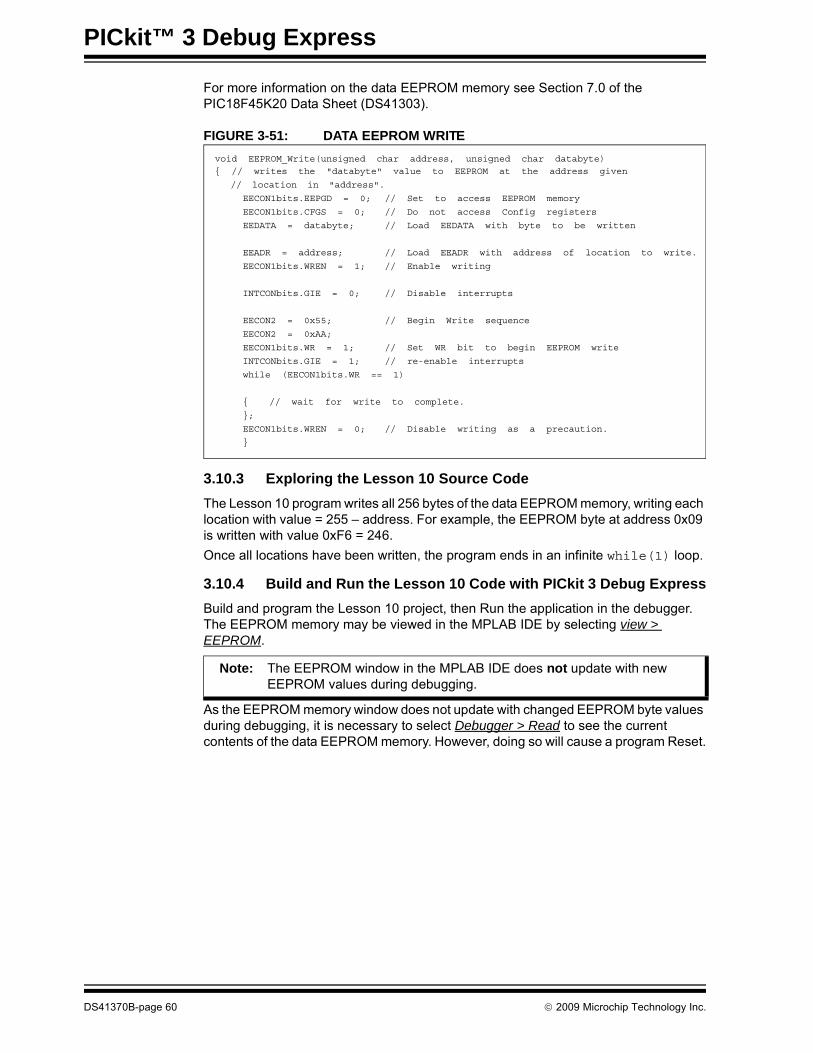
PICkit™ 3 Debug Express
For more information on the data EEPROM memory see Section 7.0 of the PIC18F45K20 Data Sheet (DS41303).
FIGURE 3-51: DATA EEPROM WRITE
3.10.3 Exploring the Lesson 10 Source CodeThe Lesson 10 program writes all 256 bytes of the data EEPROM memory, writing each location with value = 255 – address. For example, the EEPROM byte at address 0x09 is written with value 0xF6 = 246.Once all locations have been written, the program ends in an infinite while(1) loop.
3.10.4 Build and Run the Lesson 10 Code with PICkit 3 Debug ExpressBuild and program the Lesson 10 project, then Run the application in the debugger. The EEPROM memory may be viewed in the MPLAB IDE by selecting view > EEPROM.
As the EEPROM memory window does not update with changed EEPROM byte values during debugging, it is necessary to select Debugger > Read to see the current contents of the data EEPROM memory. However, doing so will cause a program Reset.
void EEPROM_Write(unsigned char address, unsigned char databyte)
// writes the "databyte" value to EEPROM at the address given
// location in "address".
EECON1bits.EEPGD = 0; // Set to access EEPROM memory
EECON1bits.CFGS = 0; // Do not access Config registers
EEDATA = databyte; // Load EEDATA with byte to be written
EEADR = address; // Load EEADR with address of location to write.
EECON1bits.WREN = 1; // Enable writing
INTCONbits.GIE = 0; // Disable interrupts
EECON2 = 0x55; // Begin Write sequence
EECON2 = 0xAA;
EECON1bits.WR = 1; // Set WR bit to begin EEPROM write
INTCONbits.GIE = 1; // re-enable interrupts
while (EECON1bits.WR == 1)
// wait for write to complete.
;
EECON1bits.WREN = 0;
// Disable writing as a precaution.
Note: The EEPROM window in the MPLAB IDE does not update with new EEPROM values during debugging.
DS41370B-page 60 © 2009 Microchip Technology Inc.

PICkit™ 3 Debug Express Lessons
3.11 LESSON 11: PROGRAM MEMORY OPERATIONSTopics covered in this include reading, writing and erasing locations in the Flash program memory, protecting areas of program memory in the Configuration bits, and considerations for using C pointers to program memory.
The MPLAB C Compiler simplifies working with data stored in program memory by allowing pointers to program memory to be declared. The pointer address length is either 16 or 24 bits, depending on which “Code Model” is selected in the project settings. The “Small Code Model” will generate 16-bit pointers, while the “Large Code Model” generates 24-bit pointers. For the best microcontroller performance, the “Small Code Model” with 16-bit pointers should be used. The “Large Code Model” is necessary for devices that have more than 64 KB of Flash program memory to be able to point to locations above the first 64 KB of program memory. (The maximum of a 16-bit value is 65536, which is 64 x 1024 or 64K).The Code Model settings may be changed in the MPLAB IDE by selecting Project > Build Options… > Project. This brings up the Build Options dialog. Select the MPLAB C18 tab and then “Memory Model” from the “Categories” drop-down box as shown in Figure 3-52.An individual pointer declaration may also use the keywords near or far to explicitly specify the pointer address length. Use of either keyword overrides the code model settings.near rom char *rom_pointer; // 16-bit pointer to program memory far
rom char *rom_pointer; // 24-bit pointer to program memory
For more information on project memory models, see Chapter 3 of the “MPLAB C18 C Compiler User’s Guide” (DS51288).
Key Concepts- Pointers declared with the ROM keyword point to program memory loca-
tions. - The EECON1 and EECON2 SFRs control program memory erase and write
operations. - Unlike Data EEPROM memory, the Flash program memory must be explic-
itly erased before it may be written. - The CPx (code-protect) Configuration bits prevent programmers from read-
ing ranges of a microcontroller’s program memory. - The WRTx Configuration bits prevent software write operations on ranges of
program memory, and the EBTRx bits prevent software read operations on ranges of program memory.
- ROM pointers and reading Flash program memory
© 2009 Microchip Technology Inc. DS41370B-page 61

PICkit™ 3 Debug Express
FIGURE 3-52: PROJECT CODE MODEL SETTINGS
Once a pointer to program memory has been declared, it can be pointed to a declared location in program memory, for example a #pragma romdata array, or an explicit address.#pragma romdata mystrings = 0x100
rom char hello_str[] = "Hello!";
rom_pointer = hello_str; // = &hello_str[0]
char letter = *rom_pointer
The first letter ‘H’ of the hello_str[] array in program memory is now pointed to by rom_pointer. The value of the variable letter is now ‘H’rom_pointer = (near rom char *)0x320;
Now, rom_pointer points to the program memory byte at address 0x320.Reading Flash program memory then simply requires declaring a ROM pointer and using an assignment statement to read the pointer value.
DS41370B-page 62 © 2009 Microchip Technology Inc.

PICkit™ 3 Debug Express Lessons
3.11.1 Erasing and Writing Flash Program MemoryUnlike writing Data EEPROM Memory, writing Flash program memory requires that the locations being written are erased first. When erased, a program memory location has all bits set to ‘1’. Thus an erased byte has the hex value 0xFF. Writing a program memory location sets the appropriate bits to ‘0’, but a write cannot set a bit ‘1’. Also different from EEPROM operations is that program memory erases and writes cannot operate on a single byte, but instead operation on “blocks” of a particular number of bytes.The PIC18F45K20 erase block size is 64 bytes. This means it will always erase 64 sequential bytes at once, and the block must start at an address that is a multiple of 64. For example, we could erase the 64 bytes from address 128 through 191 at once, but not the 64 bytes from address 100 through 163.To erase a 64 byte block of program memory, we use a rom pointer to set the address of the block to be erased, and use EECON1 to control the erase. Setting the pointer address puts the address in the TBLPTRx Special Function Registers. These 3 registers hold the address for program memory operations with TBLRD and TBLWR assembly instructions. The MPLAB C Compiler handles these tasks for us. The EEPGD bit, EECON1, is set to ‘1’, so the operation affects program memory and not data EEPROM. The CFGS bit is set to ‘0’, as we do not want to select the Configuration bits. To select an erase operation as opposed to a write operation, bit FREE of EECON1 is set to ‘1’. WREN is then set to ‘1’ to enable write/erase operations.// point to address 2176, which is a multiple of 64
rom_pointer = (near rom char *)0x880;
EECON1bits.EEPGD = 1; // point to flash program memory
EECON1bits.CFGS = 0; // not configuration registers
EECON1bits.FREE = 1; // we're erasing
EECON1bits.WREN = 1; // enable write/erase operations
Next, the EECON2 sequence must be followed as with data EEPROM writes, and the WR bit of EECON1 is set to initiate the write.INTCONbits.GIE = 0; // Disable interrupts
EECON2 = 0x55; // Begin Write sequence
EECON2 = 0xAA;
EECON1bits.WR = 1; // Set WR bit to begin EEPROM write
INTCONbits.GIE = 1; // re-enable interrupts
As with a data EEPROM write, an erase or write to Flash program memory takes up to several ms to complete. While there is an active erase or a write operation to program memory, all microcontroller program execution is halted since it is possible the microcontroller might attempt to execute instructions from the locations being erased or written. This would be illegal, as the program memory location’s value is in an indeterminate state until the operation has completed.The PIC18F45K20 write block size is 32 bytes. This requires that we write 32 sequential bytes at a time. As with erasing, the first byte must be at an address that is a multiple of the block size, 32.The sequence for writing program memory is very similar to that for erasing. The differences are that a ROM pointer is used to write the 32 locations, and that the EECON1 bit, FREE, is cleared to select a write operation. Don’t forget that the locations to be written must be erased first!
© 2009 Microchip Technology Inc. DS41370B-page 63

PICkit™ 3 Debug Express
When the 32 locations are written with the pointer, they are not actually written to program until the completion of the entire sequence. The pointer writes actually store the data in 32 temporary hardware registers. When the actual write sequence is executed, it is the contents of this 32-byte buffer that is written to the program memory array. For example, we might use a for loop to write the contents of a RAM array to these buffers using a ROM pointer.for (i = 0; i < 32; i++)*(rom_pointer + i) = ram_array[i];// write to the holding registers
This data is not actually in program memory yet, and won’t be until the entire write sequence is completed as shown in Figure 3-51.
As an example for the above note, suppose using the following code we intended to write to the 32 block of program memory from address 0x100 to 0x11F. The data would actually be written to address 0x120 because the pointer is incremented to address 0x120 after the last write.rom_pointer = (near rom unsigned char *)0x100;
for (i = 0; i < 32; i++)*(rom_pointer++) = ram_array[i]; // write to the holding registers// after the for loop, the rom_pointer address value is 0x120.
If the rom_pointer value were left at 0x11F, the data would be written as intended started at 0x100.
Note: The program memory block that is written to is determined by the address in the TBLPTRU:TBLPTRH:TBLPRTL Special Function Registers, exclud-ing the 5 Least Significant bits. These bits are excluded to ensure the write block begins on a 32-byte boundary. Therefore, it is critically important that the pointer address is not incremented past the last address in the block. If this occurs, the 32 bytes will be written at the next block boundary instead of the intended one.
DS41370B-page 64 © 2009 Microchip Technology Inc.

PICkit™ 3 Debug Express Lessons
FIGURE 3-53: EXAMPLE PROGRAM MEMORY WRITE FUNCTION
3.11.2 Protecting Program Memory in the Configuration Bits.The program is divided into sections that can individually be protected by setting the appropriate Configuration bits. The protections available are:
Code Protect – The CPx bits prevent microcontroller programmers such as the PICkit 3 from reading the contents of program memory in the address range asso-ciated with the particular CPx Configuration bit. If a programmer attempts to read a code-protected section of memory, all locations will read as value 0x00. This prevents other parties from stealing proprietary program code.Write Protect – When a WRTx Configuration bit is ON, then program memory erase or write operations are prohibited from working on the associated range of memory. This could be used to protect a bootloader from accidental corruption by inadvertent application program memory writes or erases.Table Read Protect – The EBTRx bits, when asserted, prevent program memory locations being read from instructions executing in another program memory block. For example, if EBTR3 was asserted, then program memory locations from 0x6000 to 0x7FFF by any code executing from program memory locations 0x0000 to 0x5FFF. Locations in the block 0x6000 to 0x7FFF could still be read by code executing in that block. This could be used, for example, to prevent using a boot-loader to read out sensitive code-protected data.
Once these protective Configuration bits have been asserted (set to ON), they cannot be turned off or changed without a programmer executing a Bulk Erase on the microcontroller, which erases all program memory and data EEPROM memory. It is possible to prevent other Configuration bits from being changed after the device is initially programmed using the WRTC Configuration bit.
unsigned char ProgMemWr32(unsigned int address, unsigned char *buffer_ptr)
// NOTE: program memory must also be erased first.
near rom unsigned char *ptr;
char i;
ptr = (rom unsigned char *)(address & 0xFFE0);// ensure write starts on 32-byte boundary
for (i = 0; i < 32; i++)
*(ptr + i) = buffer_ptr[i]; // write the data into the holding registers
EECON1bits.EEPGD = 1; // write to flash program memory
EECON1bits.CFGS = 0; // not configuration registers
EECON1bits.FREE = 0; // we're not erasing now.
EECON1bits.WREN = 1; // enable write/erase operations
// execute code sequence, which cannot be interrupted, then execute write32
INTCONbits.GIE = 0; // Disable interrupts
EECON2 = 0x55; // Begin Write sequence
EECON2 = 0xAA;
EECON1bits.WR = 1; // Set WR bit to begin 32-byte write
INTCONbits.GIE = 1; // re-enable interrupts
EECON1bits.WREN = 0; // disable write/erase operations
© 2009 Microchip Technology Inc. DS41370B-page 65

PICkit™ 3 Debug Express
3.11.3 Exploring the Lesson 11 Source Code with PICkit 3 Debug Express
At compile time, when the project is built, the Lesson 11 source code places three strings in Flash program memory at address 0x100:#pragma romdata mystrings = 0x100
rom char hello_str[] = "Hello!";
rom char mchp_str[] = "Microchip"; rom char fill_60[] =
"012345678901234567890123456789012345678901234567890123456789";
After building the project, the strings can be seen in program memory by opening the Program Memory window in the MPLAB IDE using View > Program Memory.
FIGURE 3-54: STRINGS IN PROGRAM MEMORY
The program code doesn’t start until address 0x280.Build and program the Lesson 11 code and set a breakpoint on the first pointer assignment statement as shown in Figure 3-55.
FIGURE 3-55: BREAKPOINT ON POINTER ASSIGNMENT
Run the program until it stops at the breakpoint. Step through the do while loop in Figure 3-55 and observe the characters of the hello_str[] string are read into the singlechar variable one at a time until the terminating ‘0’ value of the string is reached.The next statement demonstrates reading from an explicit program memory address using a function:singlechar = ProgMemRdAddress(0x107); // returns 'M' from "Microchip".
DS41370B-page 66 © 2009 Microchip Technology Inc.

PICkit™ 3 Debug Express Lessons
Step into the following statement and through the function, which erases a 64-byte block of memory that the strings are stored in.// Erase the 64 bytes starting at 0x100
ProgMemErase64(0x100);
After completing the erase, select menu Debugger > Read. In the Program Memory window, the 64 bytes of program memory starting at address 0x0100 where the strings were stored have been erased, as shown in Figure 3-56.
FIGURE 3-56: ERASED 0X0100 TO 0X013F
The remaining code creates a 32-byte buffer in RAM and fills it with the alphabet characters in uppercase, plus a few punctuation characters at the end. This buffer is then written to the 32-byte block of program memory starting at 0x0100 that was just erased. Since we read program memory, we’ll have to reset the debugger. Select Debugger > Reset > Processor Reset. Right-click on the source code and select Breakpoints > Remove All Breakpoints from the pop-up menu to clear the breakpoint we set earlier. Run the program. After running for a few seconds, select Debugger > Halt. The program should be stopped at final while(1) loop. Select Debugger > Read again and we can see that the write to program memory was successful.
FIGURE 3-57: PROGRAM MEMORY WRITE RESULTS
© 2009 Microchip Technology Inc. DS41370B-page 67

PICkit™ 3 Debug Express
3.12 LESSON 12: USING THE CCP MODULE PWMThis lesson gives a brief introduction to using the Pulse Width Modulation (PWM) functionality of the Capture/Compare/PWM (CCP) peripheral of the PIC18F45K20.
3.12.1 PWM Overview In short, Pulse Width Modulation is a square wave of a given frequency where the duty cycle of the period is varied. The duty cycle is a ratio of how long the signal is high to the total length of the period. For example, a waveform with a frequency of 250 Hz has a period of 4ms. For a PWM signal with a 25% duty cycle, the waveform would be high for 1ms and low for 3ms (and then repeat). A PWM signal with 50% duty is high for 2ms and low for 2ms, while a 75% duty cycle would be high for 3ms and low for 1ms.
FIGURE 3-58: EXAMPLE PWM DUTY CYCLES
Pulse Width modulation is used in a variety of applications, including communications, motor control, audio and analog outputs, and lighting. In this lesson, the brightness of a demo board LED will be controlled with the output of the PWM. The LED is only on during the high portion of the PWM period, and is off during the low period. As the duty cycle is decreased, the LED is on for a shorter and shorter portion of the PWM period, so it appears dimmer. The frequency is set high enough that the human eye cannot detect the individual blinks of each period, but sees the LED light as continuously on.
3.12.2 Using the CCP ModuleTimer2 is used to set the period, or frequency, of the PWM waveform. Timer2 operation is very similar to Timer0 discussed in Lesson 5, with a few differences. Namely, Timer2 is always an 8-bit timer.
Key Concepts- The PWM time base (frequency) is determined by Timer2 and the PR2
Special Function Register. - PWM operation of the CCP module is selected in the CCPxCON SFR. - Up to 10 bits of resolution are possible, with the 8 MSbs of the duty cycle in
CCPRxL, and the 2 LSBs in CCPxCON. - The actual amount of duty cycle resolution depends on the value of the PR2
register.
DS41370B-page 68 © 2009 Microchip Technology Inc.

PICkit™ 3 Debug Express Lessons
Timer2 also has a postscaler, but the postscaler does not affect the CPP module operation PWM time base, so its settings are “don’t care.” The Timer2 module also has a Period Register, known as PR2. This Special Function Register is the maximum to which Timer2 can count before being reset to 0.Normally, an 8-bit timer would count up to 255 before resetting to 0 and beginning to count again. With the PR2 register, the timer counts up to the value in PR2. When it reaches this value, the timer is reset to 0. For example if PR2 = 3, then Timer2 would count 0-1-2-3-0-1-2-3-0-1-2-3- etc.The count cycle from zero up until Timer2 reaches the PR2 in conjunction with the timer prescaler (which determines how long each timer count takes) determines the PWM frequency. The time between each reset to 0 in Timer2 is the PWM period. For example, assume we want a PWM frequency of 62.5 Hz, which has a period of 16 ms.Our clock is the internal oscillator block default, 1 MHz, which gives a 250 kHz instruction rate. 250,000 Hz/62.5 Hz = 4000. Thus, we need to count 4000 times at 250 kHz before each Timer2 Reset. However, Timer2 is 8 bits and can count to a maximum of 255. So we must use the prescaler to slow down the counting. Timer2 has 3 prescaler options: 1:1, 1:4, or 1:16 (Figure 3-59). 4000/256 = 15.6 so it requires a prescaler of 1:16.With the prescaler set to 1:16, the count frequency of Timer2 is 250,000 Hz/16 = 15625 Hz. To get our PWM frequency of 62.5 Hz, Timer 2 must count 15625/62.5 = 250 times. Since Timer2 starts at 0, we set PR2 = 249, so it counts 0-249 (250 counts), resets to zero, and counts back to 249. A simplified diagram of the PWM module is shown in Figure 3-60.
FIGURE 3-59: T2CON: TIMER2 CONTROL REGISTER
© 2009 Microchip Technology Inc. DS41370B-page 69

PICkit™ 3 Debug Express
FIGURE 3-60: SIMPLIFIED PWM BLOCK DIAGRAM
Now that the frequency has been determined, it is necessary to set up the CCP1 module for PWM using the CCP1CON register. Bits CCP1Mx determine the module mode; there is only one value to select for PWM, CCP1Mx = 0b11xx where the ‘x’ bits are “don’t care”, so 0b1100 will work. The two DC1Bx bits in CCP1CON are the 2 Least Significant bits of the 10-bit PWM duty cycle value. The 8 Most Significant of the 10 bits are written to CCPR1L.The duty cycle value is determined by the duty cycle percentage (DC%) times the 10-bit time base (PR2 * 4). DCValue = DC% * (PR2 * 4). For example, to get a duty cycle of 50%, the value would be 50% * (250 * 4) = 500. 500 decimal is 0x1F4 hex or 0b01 1111 0100 binary. The 8 Most Significant bits, 0b01 1111 01 or 0x7D, are written to CCPR1L, and the 2 LSbs are written to the DC1B1 and DC1B0 bits in CCP1CON.
DS41370B-page 70 © 2009 Microchip Technology Inc.

PICkit™ 3 Debug Express Lessons
FIGURE 3-61: CCPXCON: CCPX CONTROL REGISTER
For more information on Timer2 see Section 13.0 “Timer2 Module” of the PIC18F45K20 Data Sheet (DS41303). More info on the CCP module PWM functionality can be found in Section 15.0 “Capture/Compare/PWM (CCP) Module”, and Section 15.4 “PWM Mode”.
3.12.3 Exploring the Lesson 12 Source CodeThe PWM signal from the CCP1 module is normally output on the CCP1/RC2 pin. However, this pin is not connected to any demo board LEDs. To output a signal on an LED pin, the Enhanced CCP module (ECCP) on the PIC18F45K20 is utilized. This functionality is selected in the upper 2 bits of CCP1CON (P1Mx), which are set to 0b01 so the modulated PWM signal appears on the P1D/RD7 which drives LED 7. No other aspect of the enhanced PWM functionality is used; for more information see Section 16.0 “Enhanced Capture/Compare/Pwm (ECCP) Module”.The first thing done in the lesson source code is to set PWM pin RD7 to an output.TRISDbits.TRISD7 = 0;
Timer2 is then configured to generate the PWM period of 16 ms as discussed previously in this lesson.T2CON = 0b00000111;// Prescale = 1:16, timer on
PR2 = 249;// Timer 2 Period Register = 250 counts
© 2009 Microchip Technology Inc. DS41370B-page 71

PICkit™ 3 Debug Express
Finally, the CCP1 module is configured for PWM operation with a duty cycle of 50% as described previously in this lesson:CCPR1L = 0x7D; // The 8 most significant bits of the period are 0x7D
CCP1CON = 0b01001100; // The 2 LSbs are 0b00, and CCP1Mx = 110 for PWM
At this point in the program in the module running, generating and outputting a PWM signal on RD7/P1D with 50% duty cycle at 62.5 Hz.To make the LED get brighter and then dimmer, we have a loop that changes the duty cycle. The first do while loop increases the brightness over 2 seconds by increasing the duty cycle. As the duty cycle is increased, the LED is on for a longer period of time so it appears brighter. Note that for simplicity, the lesson program only changes the 8 MSbs of the duty cycle value in CCPR1L.The second do while loop decreases the brightness over 2 seconds by reducing the duty cycle. As the duty cycle is decreased, the LED is on for shorter and shorter periods of time, making it appear dimmer.
3.12.4 Build and Run the Lesson 12 Code with PICkit 3 Debug ExpressBuild and program the Lesson 12 project, then Run the application in the debugger. You will see the demo board LED 7 continuously get brighter then dimmer! If you have an oscilloscope available, connect a probe to one of the RD7 signal points on the demo board to see the changing the PWM waveform.
DS41370B-page 72 © 2009 Microchip Technology Inc.

PICkit™ 3 DEBUG EXPRESS
Appendix A. Schematics
FIGURE A-1: SCHEMATIC FOR PICKIT 3 DEBUG EXPRESS 44-PIN DEMO BOARD WITH PIC18F45K20
RB
0
RA
0
RA7
RB0 RB0
R1
1KΩ
SW
1
INT
0
R2
10KΩ
R3
1KΩ
+V
C3
0.1μ
F
RP
110
KΩ
DS1
DS3
DS4
DS5
DS6
DS8
DS2
DS7
JP1
C4
22μF X1
10 M
Hz
C5
22μF
Rf
1MΩ
RA6
CEX
T0.
1μF
REX
T10
KΩ
+V
+V
C1
0.1μ
FC
20.
1μF
P1
ICSP
™
RA
0R
A1
RA
2R
A3
RA
4R
A5
RB
0R
B1
RB
2R
B3
RB
4R
B5
RB
6R
B7
RC
2R
C3
RC
4R
C5
RC
6R
C7
RD
0R
D1
RD
2R
D3
RD
4R
D5
RD
6R
D7
RE
0R
E1
RE
2
19 20 21 22 23 24 9 10 11 14 15 16 17 37 42 43 44 1 38 39 40 41 2 3 4 5 25 26 278 32 3635
PIC
® 4
4-P
IN F
AM
ILY
VD
D7 28
VD
D
18M
CLR
/VP
P
30O
SC
1/C
LKIN
31O
SC
2/C
LKO
UT
12N
C13
NC
33N
C
34N
C
6V
SS
29V
SS
RA
0/A
N0
RA
1/A
N1
RA
2/A
N2/
VR
EF-
RA
3/A
N3/
VR
EF+
RA
4/T0
CK
1R
A5/
AN
4/S
SR
B0/
INT0
RB
1/IN
T1R
B2/
INT2
RB
3R
B4
RB
5R
B6/
PG
0R
B7/
PG
0
RC
0/T
10S
0/T1
CK
1
RC
1/T1
0S1/
CC
P2
RC
2/C
CP
1R
C3/
SC
K/S
CL
RC
4/S
01/S
OA
RC
5/S
O0
RC
6/TX
/CK
RC
7/R
X/O
T
RD
0/P
SP
0R
D1/
PS
P1
RD
2/P
SP
2R
D3/
PS
P3
RD
4/P
SP
4R
D5/
PS
P5
RD
6/P
SP
6R
D7/
PS
P7
RE
0/R
O/A
N5
RE
1/W
R/A
N6
RE
2/C
S/A
N7
C16
12μF
C7
12μF
X232
kH
zR
422
0KΩ
R5
750K
Ω
R6
750K
Ω
R7
750K
Ω
R8
750K
Ω
R9
750K
Ω
R10
750K
Ω
R11
750K
Ω
R12
750K
Ω
U1
21
P2
PW
R+V
RD2
RD3
RD4
RD5
RD7
RD0
RD1
RD6
VPP
VD
DG
ND
ICS
PDA
TIC
SPC
LKA
UX
AUX
1 2 3 4 5 6
© 2009 Microchip Technology Inc. DS41370B-page 73

DS41370B-page 74 © 2009 Microchip Technology Inc.
AMERICASCorporate Office2355 West Chandler Blvd.Chandler, AZ 85224-6199Tel: 480-792-7200 Fax: 480-792-7277Technical Support: http://support.microchip.comWeb Address: www.microchip.comAtlantaDuluth, GA Tel: 678-957-9614 Fax: 678-957-1455BostonWestborough, MA Tel: 774-760-0087 Fax: 774-760-0088ChicagoItasca, IL Tel: 630-285-0071 Fax: 630-285-0075DallasAddison, TX Tel: 972-818-7423 Fax: 972-818-2924DetroitFarmington Hills, MI Tel: 248-538-2250Fax: 248-538-2260KokomoKokomo, IN Tel: 765-864-8360Fax: 765-864-8387Los AngelesMission Viejo, CA Tel: 949-462-9523 Fax: 949-462-9608Santa ClaraSanta Clara, CA Tel: 408-961-6444Fax: 408-961-6445TorontoMississauga, Ontario, CanadaTel: 905-673-0699 Fax: 905-673-6509
ASIA/PACIFICAsia Pacific OfficeSuites 3707-14, 37th FloorTower 6, The GatewayHarbour City, KowloonHong KongTel: 852-2401-1200Fax: 852-2401-3431Australia - SydneyTel: 61-2-9868-6733Fax: 61-2-9868-6755China - BeijingTel: 86-10-8528-2100 Fax: 86-10-8528-2104China - ChengduTel: 86-28-8665-5511Fax: 86-28-8665-7889China - Hong Kong SARTel: 852-2401-1200 Fax: 852-2401-3431China - NanjingTel: 86-25-8473-2460Fax: 86-25-8473-2470China - QingdaoTel: 86-532-8502-7355Fax: 86-532-8502-7205China - ShanghaiTel: 86-21-5407-5533 Fax: 86-21-5407-5066China - ShenyangTel: 86-24-2334-2829Fax: 86-24-2334-2393China - ShenzhenTel: 86-755-8203-2660 Fax: 86-755-8203-1760China - WuhanTel: 86-27-5980-5300Fax: 86-27-5980-5118China - XiamenTel: 86-592-2388138 Fax: 86-592-2388130China - XianTel: 86-29-8833-7252Fax: 86-29-8833-7256China - ZhuhaiTel: 86-756-3210040 Fax: 86-756-3210049
ASIA/PACIFICIndia - BangaloreTel: 91-80-3090-4444 Fax: 91-80-3090-4080India - New DelhiTel: 91-11-4160-8631Fax: 91-11-4160-8632India - PuneTel: 91-20-2566-1512Fax: 91-20-2566-1513Japan - YokohamaTel: 81-45-471- 6166 Fax: 81-45-471-6122Korea - DaeguTel: 82-53-744-4301Fax: 82-53-744-4302Korea - SeoulTel: 82-2-554-7200Fax: 82-2-558-5932 or 82-2-558-5934Malaysia - Kuala LumpurTel: 60-3-6201-9857Fax: 60-3-6201-9859Malaysia - PenangTel: 60-4-227-8870Fax: 60-4-227-4068Philippines - ManilaTel: 63-2-634-9065Fax: 63-2-634-9069SingaporeTel: 65-6334-8870Fax: 65-6334-8850Taiwan - Hsin ChuTel: 886-3-572-9526Fax: 886-3-572-6459Taiwan - KaohsiungTel: 886-7-536-4818Fax: 886-7-536-4803Taiwan - TaipeiTel: 886-2-2500-6610 Fax: 886-2-2508-0102Thailand - BangkokTel: 66-2-694-1351Fax: 66-2-694-1350
EUROPEAustria - WelsTel: 43-7242-2244-39Fax: 43-7242-2244-393Denmark - CopenhagenTel: 45-4450-2828 Fax: 45-4485-2829France - ParisTel: 33-1-69-53-63-20 Fax: 33-1-69-30-90-79Germany - MunichTel: 49-89-627-144-0 Fax: 49-89-627-144-44Italy - Milan Tel: 39-0331-742611 Fax: 39-0331-466781Netherlands - DrunenTel: 31-416-690399 Fax: 31-416-690340Spain - MadridTel: 34-91-708-08-90Fax: 34-91-708-08-91UK - WokinghamTel: 44-118-921-5869Fax: 44-118-921-5820
WORLDWIDE SALES AND SERVICE
01/16/09