pic18f6520/8520/6620/8620/6720/8720 data...
TRANSCRIPT

2004 Microchip Technology Inc. DS39609B
PIC18F6520/8520/6620/8620/6720/8720Data Sheet
64/80-Pin High-Performance,256 Kbit to 1 Mbit Enhanced Flash
Microcontrollers with A/D
Note the following details of the code protection feature on Microchip devices:
• Microchip products meet the specification contained in their particular Microchip Data Sheet.
• Microchip believes that its family of products is one of the most secure families of its kind on the market today, when used in the intended manner and under normal conditions.
• There are dishonest and possibly illegal methods used to breach the code protection feature. All of these methods, to our knowledge, require using the Microchip products in a manner outside the operating specifications contained in Microchip's Data Sheets. Most likely, the person doing so is engaged in theft of intellectual property.
• Microchip is willing to work with the customer who is concerned about the integrity of their code.
• Neither Microchip nor any other semiconductor manufacturer can guarantee the security of their code. Code protection does not mean that we are guaranteeing the product as “unbreakable.”
Code protection is constantly evolving. We at Microchip are committed to continuously improving the code protection features of ourproducts. Attempts to break Microchip’s code protection feature may be a violation of the Digital Millennium Copyright Act. If such actsallow unauthorized access to your software or other copyrighted work, you may have a right to sue for relief under that Act.
Information contained in this publication regarding deviceapplications and the like is intended through suggestion onlyand may be superseded by updates. It is your responsibility toensure that your application meets with your specifications.No representation or warranty is given and no liability isassumed by Microchip Technology Incorporated with respectto the accuracy or use of such information, or infringement ofpatents or other intellectual property rights arising from suchuse or otherwise. Use of Microchip’s products as criticalcomponents in life support systems is not authorized exceptwith express written approval by Microchip. No licenses areconveyed, implicitly or otherwise, under any intellectualproperty rights.
DS39609B-page ii
Trademarks
The Microchip name and logo, the Microchip logo, Accuron, dsPIC, KEELOQ, MPLAB, PIC, PICmicro, PICSTART, PRO MATE and PowerSmart are registered trademarks of Microchip Technology Incorporated in the U.S.A. and other countries.
AmpLab, FilterLab, microID, MXDEV, MXLAB, PICMASTER, SEEVAL, SmartShunt and The Embedded Control Solutions Company are registered trademarks of Microchip Technology Incorporated in the U.S.A.
Application Maestro, dsPICDEM, dsPICDEM.net, dsPICworks, ECAN, ECONOMONITOR, FanSense, FlexROM, fuzzyLAB, In-Circuit Serial Programming, ICSP, ICEPIC, microPort, Migratable Memory, MPASM, MPLIB, MPLINK, MPSIM, PICkit, PICDEM, PICDEM.net, PICtail, PowerCal, PowerInfo, PowerMate, PowerTool, rfLAB, rfPIC, Select Mode, SmartSensor, SmartTel and Total Endurance are trademarks of Microchip Technology Incorporated in the U.S.A. and other countries.
Serialized Quick Turn Programming (SQTP) is a service mark of Microchip Technology Incorporated in the U.S.A.
All other trademarks mentioned herein are property of their respective companies.
© 2004, Microchip Technology Incorporated, Printed in the U.S.A., All Rights Reserved.
Printed on recycled paper.
2004 Microchip Technology Inc.
Microchip received ISO/TS-16949:2002 quality system certification for its worldwide headquarters, design and wafer fabrication facilities in Chandler and Tempe, Arizona and Mountain View, California in October 2003. The Company’s quality system processes and procedures are for its PICmicro® 8-bit MCUs, KEELOQ® code hopping devices, Serial EEPROMs, microperipherals, nonvolatile memory and analog products. In addition, Microchip’s quality system for the design and manufacture of development systems is ISO 9001:2000 certified.

PIC18F6520/8520/6620/8620/6720/8720
64/80-Pin High-Performance, 256 Kbit to 1 Mbit Enhanced Flash Microcontrollers with A/D
High-Performance RISC CPU:• C compiler optimized architecture/instruction set:
- Source code compatible with the PIC16 and PIC17 instruction sets
• Linear program memory addressing to 128 Kbytes• Linear data memory addressing to 3840 bytes • 1 Kbyte of data EEPROM• Up to 10 MIPs operation:
- DC – 40 MHz osc./clock input- 4 MHz – 10 MHz osc./clock input with PLL active
• 16-bit wide instructions, 8-bit wide data path• Priority levels for interrupts • 31-level, software accessible hardware stack• 8 x 8 Single Cycle Hardware Multiplier
External Memory Interface(PIC18F8X20 Devices Only):• Address capability of up to 2 Mbytes• 16-bit interface
Peripheral Features:• High current sink/source 25 mA/25 mA• Four external interrupt pins• Timer0 module: 8-bit/16-bit timer/counter • Timer1 module: 16-bit timer/counter • Timer2 module: 8-bit timer/counter • Timer3 module: 16-bit timer/counter • Timer4 module: 8-bit timer/counter • Secondary oscillator clock option – Timer1/Timer3• Five Capture/Compare/PWM (CCP) modules:
- Capture is 16-bit, max. resolution 6.25 ns (TCY/16)- Compare is 16-bit, max. resolution 100 ns (TCY)- PWM output: PWM resolution is 1 to 10-bit
• Master Synchronous Serial Port (MSSP) module with two modes of operation:- 3-wire SPI™ (supports all 4 SPI modes)- I2C™ Master and Slave mode
• Two Addressable USART modules:- Supports RS-485 and RS-232
• Parallel Slave Port (PSP) module
Analog Features:• 10-bit, up to 16-channel Analog-to-Digital
Converter (A/D): - Conversion available during Sleep
• Programmable 16-level Low-Voltage Detection (LVD) module:- Supports interrupt on Low-Voltage Detection
• Programmable Brown-out Reset (PBOR)• Dual analog comparators:
- Programmable input/output configuration
Special Microcontroller Features:• 100,000 erase/write cycle Enhanced Flash
program memory typical• 1,000,000 erase/write cycle Data EEPROM
memory typical• 1 second programming time• Flash/Data EEPROM Retention: > 40 years• Self-reprogrammable under software control• Power-on Reset (POR), Power-up Timer (PWRT)
and Oscillator Start-up Timer (OST)• Watchdog Timer (WDT) with its own On-Chip
RC Oscillator for reliable operation• Programmable code protection• Power saving Sleep mode• Selectable oscillator options including:
- 4X Phase Lock Loop (of primary oscillator)- Secondary Oscillator (32 kHz) clock input
• In-Circuit Serial Programming™ (ICSP™) via two pins
• MPLAB® In-Circuit Debug (ICD) via two pins
CMOS Technology:• Low-power, high-speed Flash technology• Fully static design• Wide operating voltage range (2.0V to 5.5V) • Industrial and Extended temperature ranges
Device
Program Memory Data Memory
I/O10-bit A/D (ch)
CCP (PWM)
MSSP
USARTTimers
8-bit/16-bitExt Bus
MaxFOSC
(MHz)Bytes# Single-Word Instructions
SRAM (bytes)
EEPROM (bytes)
SPI Master
I2C
PIC18F6520 32K 16384 2048 1024 52 12 5 Y Y 2 2/3 N 40
PIC18F6620 64K 32768 3840 1024 52 12 5 Y Y 2 2/3 N 25
PIC18F6720 128K 65536 3840 1024 52 12 5 Y Y 2 2/3 N 25
PIC18F8520 32K 16384 2048 1024 68 16 5 Y Y 2 2/3 Y 40
PIC18F8620 64K 32768 3840 1024 68 16 5 Y Y 2 2/3 Y 25
PIC18F8720 128K 65536 3840 1024 68 16 5 Y Y 2 2/3 Y 25
2004 Microchip Technology Inc. DS39609B-page 1

PIC18F6520/8520/6620/8620/6720/8720
Pin Diagrams
PIC18F6620
1
2
3
4
56
7
8
9
1011
12
1314
38
37
3635
34
33
50 49
17 18 19 20 21 22 23 24 25 26
RE
2/C
S
RE
3
RE
4
RE
5
RE
6
RE
7/C
CP
2(1)
RD
0/P
SP
0
VD
D
VS
S
RD
1/P
SP
1
RD
2/P
SP
2
RD
3/P
SP
3
RD
4/P
SP
4
RD
5/P
SP
5
RD
6/P
SP
6
RD
7/P
SP
7
RE1/WRRE0/RD
RG0/CCP3RG1/TX2/CK2
RG2/RX2/DT2
RG3/CCP4
MCLR/VPP
RG4/CCP5
VSS
VDD
RF7/SSRF6/AN11
RF4/AN9
RF3/AN8RF2/AN7/C1OUT
RB0/INT0RB1/INT1
RB2/INT2
RB3/INT3RB4/KBI0
RB5/KBI1/PGM
RB6/KBI2/PGC
VSS
OSC2/CLKO/RA6OSC1/CLKI
VDD
RB7/KBI3/PGD
RC4/SDI/SDA
RC3/SCK/SCLRC2/CCP1
RF
0/A
N5
RF
1/A
N6/
C2O
UT
AV
DD
AV
SS
RA
3/A
N3/
VR
EF+
RA
2/A
N2/
VR
EF-
RA
1/A
N1
RA
0/A
N0
VS
S
VD
D
RA
4/T
0CK
I
RA
5/A
N4/
LVD
IN
RC
1/T
1OS
I/CC
P2(1
)
RC
0/T
1OS
O/T
13C
KI
RC
7/R
X1/
DT
1
RC
6/T
X1/
CK
1
RC5/SDO
15
16
31
40
39
27 28 29 30 32
48
47
46
45
44
43
42
4154 53 52 5158 57 56 5560 5964 63 62 61
PIC18F6720
RF5/AN10/CVREF
64-Pin TQFP
PIC18F6520
Note 1: CCP2 is multiplexed with RC1 when CCP2MX is set.
DS39609B-page 2 2004 Microchip Technology Inc.
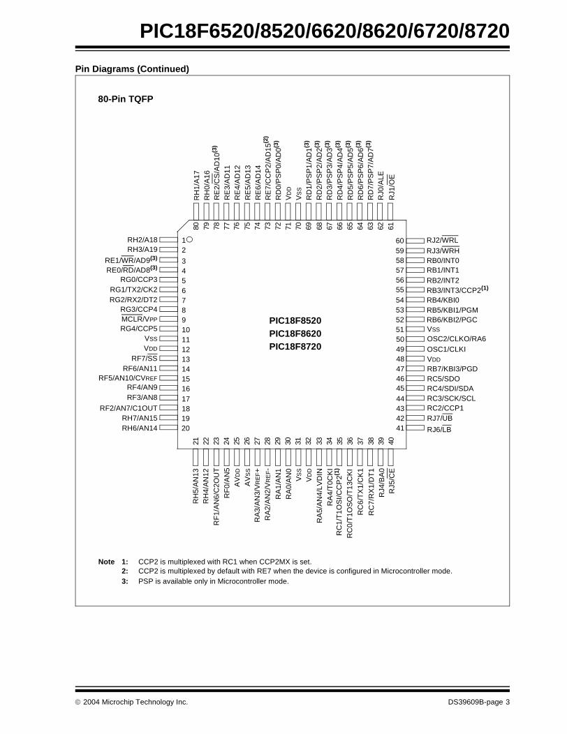
PIC18F6520/8520/6620/8620/6720/8720
Pin Diagrams (Continued)
PIC18F8620
345678910111213141516
4847464544434241
4039
64 63 62 61
21 22 23 24 25 26 27 28 29 30 31 32
RE
2/C
S/A
D10
(3)
RE
3/A
D11
RE
4/A
D12
RE
5/A
D13
RE
6/A
D14
RE
7/C
CP
2/A
D15
(2)
RD
0/P
SP
0/A
D0(3
)
VD
D
VS
S
RD
1/P
SP
1/A
D1(3
)
RD
2/P
SP
2/A
D2(3
)
RD
3/P
SP
3/A
D3(3
)
RD
4/P
SP
4/A
D4(3
)
RD
5/P
SP
5/A
D5(3
)
RD
6/P
SP
6/A
D6(3
)
RD
7/P
SP
7/A
D7(3
)
RE1/WR/AD9(3)
RE0/RD/AD8(3)
RG0/CCP3RG1/TX2/CK2RG2/RX2/DT2
RG3/CCP4MCLR/VPP
RG4/CCP5VSS
VDD
RF7/SSRF6/AN11
RF5/AN10/CVREF
RF4/AN9RF3/AN8
RF2/AN7/C1OUT
RB0/INT0RB1/INT1RB2/INT2RB3/INT3/CCP2(1)
RB4/KBI0RB5/KBI1/PGMRB6/KBI2/PGCVSS
OSC2/CLKO/RA6OSC1/CLKIVDD
RB7/KBI3/PGD
RC4/SDI/SDARC3/SCK/SCLRC2/CCP1
RF
0/A
N5
RF
1/A
N6/
C2O
UT
AV
DD
AV
SS
RA
3/A
N3/
VR
EF+
RA
2/A
N2/
VR
EF-
RA
1/A
N1
RA
0/A
N0
VS
S
VD
D
RA
4/T
0CK
IR
A5/
AN
4/LV
DIN
RC
1/T
1OS
I/CC
P2(1
)
RC
7/R
X1/
DT
1
RC
6/T
X1/
CK
1
RC5/SDOR
J0/A
LE
RJ1
/OE
RH
1/A
17R
H0/
A16
12
RH2/A18RH3/A19
1718
RH7/AN15RH6/AN14
RH
5/A
N13
RH
4/A
N12
RJ5
/CE
RJ4
/BA
0
37
RJ7/UB
RJ6/LB
5049
RJ2/WRL
RJ3/WRH
1920
33 34 35 36 38
5857565554535251
6059
68 67 66 6572 71 70 6974 7378 77 76 757980
80-Pin TQFP
PIC18F8720R
C0/
T1O
SO
/T13
CK
I
PIC18F8520
Note 1: CCP2 is multiplexed with RC1 when CCP2MX is set.2: CCP2 is multiplexed by default with RE7 when the device is configured in Microcontroller mode.3: PSP is available only in Microcontroller mode.
2004 Microchip Technology Inc. DS39609B-page 3

PIC18F6520/8520/6620/8620/6720/8720
Table of Contents
1.0 Device Overview .......................................................................................................................................................................... 72.0 Oscillator Configurations ............................................................................................................................................................ 213.0 Reset .......................................................................................................................................................................................... 294.0 Memory Organization ................................................................................................................................................................. 395.0 Flash Program Memory.............................................................................................................................................................. 616.0 External Memory Interface ......................................................................................................................................................... 717.0 Data EEPROM Memory ............................................................................................................................................................. 798.0 8 X 8 Hardware Multiplier ........................................................................................................................................................... 859.0 Interrupts .................................................................................................................................................................................... 8710.0 I/O Ports ................................................................................................................................................................................... 10311.0 Timer0 Module ......................................................................................................................................................................... 13112.0 Timer1 Module ......................................................................................................................................................................... 13513.0 Timer2 Module ......................................................................................................................................................................... 14114.0 Timer3 Module ......................................................................................................................................................................... 14315.0 Timer4 Module ......................................................................................................................................................................... 14716.0 Capture/Compare/PWM (CCP) Modules ................................................................................................................................. 14917.0 Master Synchronous Serial Port (MSSP) Module .................................................................................................................... 15718.0 Addressable Universal Synchronous Asynchronous Receiver Transmitter (USART).............................................................. 19719.0 10-Bit Analog-to-Digital Converter (A/D) Module ..................................................................................................................... 21320.0 Comparator Module.................................................................................................................................................................. 22321.0 Comparator Voltage Reference Module................................................................................................................................... 22922.0 Low-Voltage Detect .................................................................................................................................................................. 23323.0 Special Features of the CPU.................................................................................................................................................... 23924.0 Instruction Set Summary .......................................................................................................................................................... 25925.0 Development Support............................................................................................................................................................... 30126.0 Electrical Characteristics .......................................................................................................................................................... 30727.0 DC and AC Characteristics Graphs and Tables....................................................................................................................... 34328.0 Packaging Information.............................................................................................................................................................. 357Appendix A: Revision History............................................................................................................................................................. 361Appendix B: Device Differences......................................................................................................................................................... 361Appendix C: Conversion Considerations ........................................................................................................................................... 362Appendix D: Migration from Mid-Range to Enhanced Devices .......................................................................................................... 362Appendix E: Migration from High-End to Enhanced Devices............................................................................................................. 363Index .................................................................................................................................................................................................. 365On-Line Support................................................................................................................................................................................. 375Systems Information and Upgrade Hot Line ...................................................................................................................................... 375Reader Response .............................................................................................................................................................................. 376PIC18F6520/8520/6620/8620/6720/8720 Product Identification System .......................................................................................... 377
DS39609B-page 4 2004 Microchip Technology Inc.
PIC18F6520/8520/6620/8620/6720/8720
TO OUR VALUED CUSTOMERS
It is our intention to provide our valued customers with the best documentation possible to ensure successful use of your Microchipproducts. To this end, we will continue to improve our publications to better suit your needs. Our publications will be refined andenhanced as new volumes and updates are introduced.
If you have any questions or comments regarding this publication, please contact the Marketing Communications Department viaE-mail at [email protected] or fax the Reader Response Form in the back of this data sheet to (480) 792-4150.We welcome your feedback.
Most Current Data SheetTo obtain the most up-to-date version of this data sheet, please register at our Worldwide Web site at:
http://www.microchip.com
You can determine the version of a data sheet by examining its literature number found on the bottom outside corner of any page.The last character of the literature number is the version number, (e.g., DS30000A is version A of document DS30000).
ErrataAn errata sheet, describing minor operational differences from the data sheet and recommended workarounds, may exist for currentdevices. As device/documentation issues become known to us, we will publish an errata sheet. The errata will specify the revisionof silicon and revision of document to which it applies.
To determine if an errata sheet exists for a particular device, please check with one of the following:
• Microchip’s Worldwide Web site; http://www.microchip.com• Your local Microchip sales office (see last page)• The Microchip Corporate Literature Center; U.S. FAX: (480) 792-7277
When contacting a sales office or the literature center, please specify which device, revision of silicon and data sheet (include liter-ature number) you are using.
Customer Notification SystemRegister on our Web site at www.microchip.com/cn to receive the most current information on all of our products.
2004 Microchip Technology Inc. DS39609B-page 5

PIC18F6520/8520/6620/8620/6720/8720
NOTES:
DS39609B-page 6 2004 Microchip Technology Inc.

PIC18F6520/8520/6620/8620/6720/8720
1.0 DEVICE OVERVIEW
This document contains device specific information forthe following devices:
This family offers the same advantages of all PIC18microcontrollers – namely, high computationalperformance at an economical price – with the addition ofhigh endurance Enhanced Flash program memory. ThePIC18FXX20 family also provides an enhanced range ofprogram memory options and versatile analog featuresthat make it ideal for complex, high-performanceapplications.
1.1 Key Features
1.1.1 EXPANDED MEMORY
The PIC18FXX20 family introduces the widest range ofon-chip, Enhanced Flash program memory availableon PICmicro® microcontrollers – up to 128 Kbyte (or65,536 words), the largest ever offered by Microchip.For users with more modest code requirements, thefamily also includes members with 32 Kbyte or64 Kbyte.
Other memory features are:
• Data RAM and Data EEPROM: The PIC18FXX20 family also provides plenty of room for application data. Depending on the device, either 2048 or 3840 bytes of data RAM are available. All devices have 1024 bytes of data EEPROM for long-term retention of nonvolatile data.
• Memory Endurance: The Enhanced Flash cells for both program memory and data EEPROM are rated to last for many thousands of erase/write cycles – up to 100,000 for program memory and 1,000,000 for EEPROM. Data retention without refresh is conservatively estimated to be greater than 40 years.
1.1.2 EXTERNAL MEMORY INTERFACE
In the event that 128 Kbytes of program memory isinadequate for an application, the PIC18F8X20members of the family also implement an ExternalMemory Interface. This allows the controller’s internalprogram counter to address a memory space of up to2 Mbytes, permitting a level of data access that few8-bit devices can claim.
With the addition of new operating modes, the ExternalMemory Interface offers many new options, including:
• Operating the microcontroller entirely from externalmemory
• Using combinations of on-chip and externalmemory, up to the 2-Mbyte limit
• Using external Flash memory for reprogrammableapplication code, or large data tables
• Using external RAM devices for storing largeamounts of variable data
1.1.3 EASY MIGRATION
Regardless of the memory size, all devices share thesame rich set of peripherals, allowing for a smoothmigration path as applications grow and evolve.
The consistent pinout scheme used throughout theentire family also aids in migrating to the next largerdevice. This is true when moving between the 64-pinmembers, between the 80-pin members, or evenjumping from 64-pin to 80-pin devices.
1.1.4 OTHER SPECIAL FEATURES
• Communications: The PIC18FXX20 family incorporates a range of serial communications peripherals, including 2 independent USARTs and a Master SSP module, capable of both SPI and I2C (Master and Slave) modes of operation. For PIC18F8X20 devices, one of the general purpose I/O ports can be reconfigured as an 8-bit Parallel Slave Port for direct processor-to-processor communications.
• CCP Modules: All devices in the family incorporate five Capture/Compare/PWM modules to maximize flexibility in control applications. Up to four different time bases may be used to perform several different operations at once.
• Analog Features: All devices in the family feature 10-bit A/D converters, with up to 16 input channels, as well as the ability to perform conversions during Sleep mode. Also included are dual analog comparators with programmable input and output configuration, a programmable Low-Voltage Detect module and a programmable Brown-out Reset module.
• Self-programmability: These devices can write to their own program memory spaces under inter-nal software control. By using a bootloader routine located in the protected Boot Block at the top of program memory, it becomes possible to create an application that can update itself in the field.
• PIC18F6520 • PIC18F8520
• PIC18F6620 • PIC18F8620
• PIC18F6720 • PIC18F8720
2004 Microchip Technology Inc. DS39609B-page 7

PIC18F6520/8520/6620/8620/6720/8720
1.2 Details on Individual Family Members
The PIC18FXX20 devices are available in 64-pin and80-pin packages. They are differentiated from eachother in five ways:
1. Flash program memory (32 Kbytes forPIC18FX520 devices, 64 Kbytes forPIC18FX620 devices and 128 Kbytes forPIC18FX720 devices)
2. Data RAM (2048 bytes for PIC18FX520devices, 3840 bytes for PIC18FX620 andPIC18FX720 devices)
3. A/D channels (12 for PIC18F6X20 devices, 16 for PIC18F8X20)
4. I/O pins (52 on PIC18F6X20 devices, 68 onPIC18F8X20)
5. External program memory interface (presentonly on PIC18F8X20 devices)
All other features for devices in the PIC18FXX20 familyare identical. These are summarized in Table 1-1.
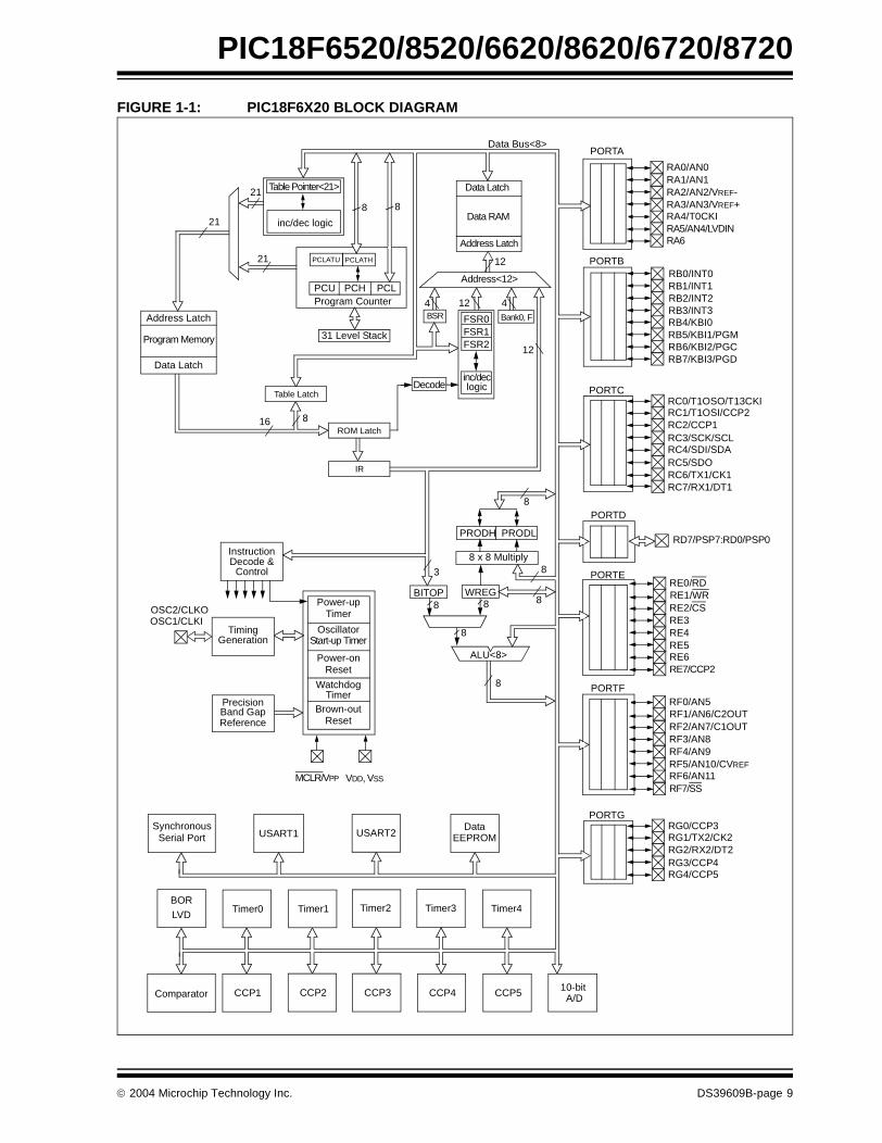
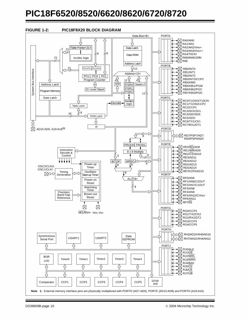
Block diagrams of the PIC18F6X20 and PIC18F8X20devices are provided in Figure 1-1 and Figure 1-2,respectively. The pinouts for these device families arelisted in Table 1-2.
TABLE 1-1: PIC18FXX20 DEVICE FEATURES
Features PIC18F6520 PIC18F6620 PIC18F6720 PIC18F8520 PIC18F8620 PIC18F8720
Operating Frequency DC – 40 MHz DC – 25 MHz DC – 25 MHz DC – 40 MHz DC – 25 MHz DC – 25 MHz
Program Memory (Bytes)
32K 64K 128K 32K 64K 128K
Program Memory (Instructions)
16384 32768 65536 16384 32768 65536
Data Memory (Bytes)
2048 3840 3840 2048 3840 3840
Data EEPROM Memory (Bytes)
1024 1024 1024 1024 1024 1024
External MemoryInterface
No No No Yes Yes Yes
Interrupt Sources 17 17 17 18 18 18
I/O Ports Ports A, B, C, D, E, F, G
Ports A, B, C, D, E, F, G
Ports A, B, C, D, E, F, G
Ports A, B, C, D, E, F, G, H, J
Ports A, B, C, D, E, F, G, H, J
Ports A, B, C, D, E, F, G, H, J
Timers 5 5 5 5 5 5
Capture/Compare/PWM Modules
5 5 5 5 5 5
Serial Communications MSSP, Addressable USART (2)
MSSP, Addressable USART (2)
MSSP, Addressable USART (2)
MSSP, Addressable USART (2)
MSSP, Addressable USART (2)
MSSP, Addressable USART (2)
Parallel Communications PSP PSP PSP PSP PSP PSP
10-bit Analog-to-Digital Module
12 input channels
12 input channels
12 input channels
16 input channels
16 input channels
16 input channels
Resets (and Delays) POR, BOR, RESET
Instruction, Stack Full,
Stack Underflow (PWRT, OST)
POR, BOR, RESET
Instruction, Stack Full,
Stack Underflow (PWRT, OST)
POR, BOR, RESET
Instruction, Stack Full,
Stack Underflow (PWRT, OST)
POR, BOR, RESET
Instruction, Stack Full,
Stack Underflow (PWRT, OST)
POR, BOR, RESET
Instruction, Stack Full,
Stack Underflow (PWRT, OST)
POR, BOR, RESET
Instruction, Stack Full,
Stack Underflow (PWRT, OST)
Programmable Low-Voltage Detect
Yes Yes Yes Yes Yes Yes
Programmable Brown-out Reset
Yes Yes Yes Yes Yes Yes
Instruction Set 77 Instructions 77 Instructions 77 Instructions 77 Instructions 77 Instructions 77 Instructions
Package 64-pin TQFP 64-pin TQFP 64-pin TQFP 80-pin TQFP 80-pin TQFP 80-pin TQFP
DS39609B-page 8 2004 Microchip Technology Inc.
PIC18F6520/8520/6620/8620/6720/8720
FIGURE 1-1: PIC18F6X20 BLOCK DIAGRAM
Power-upTimer
OscillatorStart-up Timer
Power-onReset
WatchdogTimer
InstructionDecode &
Control
OSC1/CLKIOSC2/CLKO
MCLR/VPP VDD, VSS
PORTA
PORTB
PORTC
RA4/T0CKIRA5/AN4/LVDIN
RB0/INT0
RC0/T1OSO/T13CKIRC1/T1OSI/CCP2RC2/CCP1RC3/SCK/SCLRC4/SDI/SDARC5/SDORC6/TX1/CK1RC7/RX1/DT1
Brown-outReset
USART1
Comparator
Synchronous
BOR
Serial Port
RA3/AN3/VREF+RA2/AN2/VREF-RA1/AN1RA0/AN0
TimingGeneration
RB1/INT1
Data Latch
Data RAM
Address Latch
Address<12>
12
Bank0, FBSR FSR0FSR1FSR2
inc/declogicDecode
4 12 4
PCH PCL
PCLATH
8
31 Level Stack
Program Counter
PRODLPRODH
8 x 8 Multiply
WREG
8
BITOP88
ALU<8>
8
Address Latch
Program Memory
Data Latch
21
21
16
8
8
8
Table Pointer<21>
inc/dec logic
218
Data Bus<8>
Table Latch
8
IR
12
3
ROM Latch
PORTD
RD7/PSP7:RD0/PSP0
RB2/INT2RB3/INT3
PCLATU
PCU
Precision
ReferenceBand Gap
PORTE
PORTF
PORTGRG0/CCP3RG1/TX2/CK2RG2/RX2/DT2RG3/CCP4RG4/CCP5
RF7/SS
RE6RE7/CCP2
RE5RE4RE3RE2/CS
RE0/RDRE1/WR
LVD
RA6
Timer0 Timer1 Timer2 Timer3 Timer4
CCP1 CCP2 CCP3 CCP4 CCP5
USART2
10-bit A/D
RF6/AN11RF5/AN10/CVREF
RF4/AN9RF3/AN8RF2/AN7/C1OUT
RF0/AN5RF1/AN6/C2OUT
RB4/KBI0RB5/KBI1/PGMRB6/KBI2/PGCRB7/KBI3/PGD
DataEEPROM
2004 Microchip Technology Inc. DS39609B-page 9
PIC18F6520/8520/6620/8620/6720/8720
FIGURE 1-2: PIC18F8X20 BLOCK DIAGRAM
Power-upTimer
OscillatorStart-up Timer
Power-onReset
WatchdogTimer
InstructionDecode &
Control
OSC1/CLKIOSC2/CLKO
MCLR/VPP VDD, VSS
PORTA
PORTB
PORTC
RA4/T0CKIRA5/AN4/LVDIN
RC0/T1OSO/T13CKIRC1/T1OSI/CCP2RC2/CCP1RC3/SCK/SCLRC4/SDI/SDARC5/SDORC6/TX1/CK1RC7/RX1/DT1
Brown-outReset
USART1
Comparator
Synchronous
BOR
Serial Port
RA3/AN3/VREF+RA2/AN2/VREF-RA1/AN1RA0/AN0
TimingGeneration
10-bit A/D
Data Latch
Data RAM
Address Latch
Address<12>
12
Bank0, FBSR FSR0FSR1FSR2
inc/declogicDecode
4 12 4
PCH PCL
PCLATH
8
31 Level Stack
Program Counter
PRODLPRODH
8 x 8 Multiply
WREG
8
BITOP88
ALU<8>
8
Address Latch
Program Memory
Data Latch
21
21
16
8
8
8
Table Pointer<21>
inc/dec logic
218
Data Bus<8>
Table Latch
8
IR
12
3
ROM Latch
PORTD
RD7/PSP7/AD7:
PCLATU
PCU
Precision
ReferenceBand Gap
PORTE
PORTF
PORTGRG0/CCP3RG1/TX2/CK2RG2/RX2/DT2RG3/CCP4RG4/CCP5
RF7/SS
RE6/AD14RE7/CCP2/AD15
RE5/AD13RE4/AD12RE3/AD11RE2/CS/AD10
RE0/RD/AD8RE1/WR/AD9
LVD
PORTH
PORTJRJ0/ALERJ1/OERJ2/WRLRJ3/WRH
RA6
Timer0 Timer1 Timer2 Timer3 Timer4
CCP1 CCP2 CCP3 CCP4 CCP5
USART2
Sys
tem
Bus
Inte
rfac
e
AD15:AD0, A19:A16(1)
Note 1: External memory interface pins are physically multiplexed with PORTD (AD7:AD0), PORTE (AD15:AD8) and PORTH (A19:A16).
RB0/INT0RB1/INT1RB2/INT2RB3/INT3/CCP2RB4/KBI0RB5/KBI1/PGMRB6/KBI2/PGCRB7/KBI3/PGD
RH7/AN15:RH4/AN12
RH3/AD19:RH0/AD16
RJ4/BA0RJ5/CERJ6/LBRJ7/UB
RF6/AN11RF5/AN10/CVREF
RF4/AN9RF3/AN8RF2/AN7/C1OUT
RF0/AN5RF1/AN6/C2OUT
DataEEPROM
RD0/PSP0/AD0
DS39609B-page 10 2004 Microchip Technology Inc.

PIC18F6520/8520/6620/8620/6720/8720
TABLE 1-2: PIC18FXX20 PINOUT I/O DESCRIPTIONS
Pin NamePin Number Pin
TypeBufferType
DescriptionPIC18F6X20 PIC18F8X20
MCLR/VPP
MCLR
VPP
7 9
I
P
ST
Master Clear (input) or programming voltage (output).
Master Clear (Reset) input. This pin is an active-low Reset to the device.Programming voltage input.
OSC1/CLKIOSC1
CLKI
39 49I
I
CMOS/ST
CMOS
Oscillator crystal or external clock input.Oscillator crystal input or external clock source input. ST buffer when configured in RC mode; otherwise CMOS.External clock source input. Always associated with pin function OSC1 (see OSC1/CLKI, OSC2/CLKO pins).
OSC2/CLKO/RA6OSC2
CLKO
RA6
40 50O
O
I/O
—
—
TTL
Oscillator crystal or clock output.Oscillator crystal output. Connects to crystal or resonator in Crystal Oscillator mode.In RC mode, OSC2 pin outputs CLKO, which has 1/4 the frequency of OSC1 and denotes the instruction cycle rate.General purpose I/O pin.
Legend: TTL = TTL compatible input CMOS = CMOS compatible input or output ST = Schmitt Trigger input with CMOS levels Analog = Analog input I = Input O = Output P = Power OD = Open-Drain (no P diode to VDD)
Note 1: Alternate assignment for CCP2 when CCP2MX is not selected (all operating modes except Microcontroller).
2: Default assignment when CCP2MX is set.3: External memory interface functions are only available on PIC18F8X20 devices.
4: CCP2 is multiplexed with this pin by default when configured in Microcontroller mode. Otherwise, it is multiplexed with either RB3 or RC1.
5: PORTH and PORTJ are only available on PIC18F8X20 (80-pin) devices.6: AVDD must be connected to a positive supply and AVSS must be connected to a ground reference for
proper operation of the part in user or ICSP modes. See parameter D001A for details.
2004 Microchip Technology Inc. DS39609B-page 11

PIC18F6520/8520/6620/8620/6720/8720
PORTA is a bidirectional I/O port.
RA0/AN0RA0AN0
24 30I/OI
TTLAnalog
Digital I/O.Analog input 0.
RA1/AN1RA1AN1
23 29I/OI
TTLAnalog
Digital I/O.Analog input 1.
RA2/AN2/VREF-RA2AN2VREF-
22 28I/OII
TTLAnalogAnalog
Digital I/O.Analog input 2.A/D reference voltage (Low) input.
RA3/AN3/VREF+RA3AN3VREF+
21 27I/OII
TTLAnalogAnalog
Digital I/O.Analog input 3.A/D reference voltage (High) input.
RA4/T0CKIRA4
T0CKI
28 34I/O
I
ST/OD
ST
Digital I/O – Open-drain when configured as output.Timer0 external clock input.
RA5/AN4/LVDINRA5AN4LVDIN
27 33I/OII
TTLAnalogAnalog
Digital I/O.Analog input 4.Low-Voltage Detect input.
RA6 See the OSC2/CLKO/RA6 pin.
TABLE 1-2: PIC18FXX20 PINOUT I/O DESCRIPTIONS (CONTINUED)
Pin NamePin Number Pin
TypeBufferType
DescriptionPIC18F6X20 PIC18F8X20
Legend: TTL = TTL compatible input CMOS = CMOS compatible input or output ST = Schmitt Trigger input with CMOS levels Analog = Analog input I = Input O = Output P = Power OD = Open-Drain (no P diode to VDD)
Note 1: Alternate assignment for CCP2 when CCP2MX is not selected (all operating modes except Microcontroller).
2: Default assignment when CCP2MX is set.3: External memory interface functions are only available on PIC18F8X20 devices.
4: CCP2 is multiplexed with this pin by default when configured in Microcontroller mode. Otherwise, it is multiplexed with either RB3 or RC1.
5: PORTH and PORTJ are only available on PIC18F8X20 (80-pin) devices.6: AVDD must be connected to a positive supply and AVSS must be connected to a ground reference for
proper operation of the part in user or ICSP modes. See parameter D001A for details.
DS39609B-page 12 2004 Microchip Technology Inc.

PIC18F6520/8520/6620/8620/6720/8720
PORTB is a bidirectional I/O port. PORTB can be software programmed for internal weak pull-ups on all inputs.
RB0/INT0RB0INT0
48 58I/OI
TTLST
Digital I/O.External interrupt 0.
RB1/INT1RB1INT1
47 57I/OI
TTLST
Digital I/O.External interrupt 1.
RB2/INT2RB2INT2
46 56I/OI
TTLST
Digital I/O.External interrupt 2.
RB3/INT3/CCP2RB3INT3CCP2(1)
45 55I/OI/OI/O
TTLSTST
Digital I/O.External interrupt 3.Capture2 input, Compare2 output, PWM2 output.
RB4/KBI0RB4KBI0
44 54I/OI
TTLST
Digital I/O.Interrupt-on-change pin.
RB5/KBI1/PGMRB5KBI1PGM
43 53I/OI
I/O
TTLSTST
Digital I/O.Interrupt-on-change pin.Low-Voltage ICSP Programming enable pin.
RB6/KBI2/PGCRB6KBI2PGC
42 52I/OI
I/O
TTLSTST
Digital I/O.Interrupt-on-change pin. In-Circuit Debugger and ICSP programming clock.
RB7/KBI3/PGDRB7KBI3PGD
37 47I/OI/O
TTLST
Digital I/O.Interrupt-on-change pin. In-Circuit Debugger andICSP programming data.
TABLE 1-2: PIC18FXX20 PINOUT I/O DESCRIPTIONS (CONTINUED)
Pin NamePin Number Pin
TypeBufferType
DescriptionPIC18F6X20 PIC18F8X20
Legend: TTL = TTL compatible input CMOS = CMOS compatible input or output ST = Schmitt Trigger input with CMOS levels Analog = Analog input I = Input O = Output P = Power OD = Open-Drain (no P diode to VDD)
Note 1: Alternate assignment for CCP2 when CCP2MX is not selected (all operating modes except Microcontroller).
2: Default assignment when CCP2MX is set.
3: External memory interface functions are only available on PIC18F8X20 devices.4: CCP2 is multiplexed with this pin by default when configured in Microcontroller mode. Otherwise, it is
multiplexed with either RB3 or RC1.5: PORTH and PORTJ are only available on PIC18F8X20 (80-pin) devices.6: AVDD must be connected to a positive supply and AVSS must be connected to a ground reference for
proper operation of the part in user or ICSP modes. See parameter D001A for details.
2004 Microchip Technology Inc. DS39609B-page 13

PIC18F6520/8520/6620/8620/6720/8720
PORTC is a bidirectional I/O port.
RC0/T1OSO/T13CKIRC0T1OSOT13CKI
30 36I/OOI
ST—ST
Digital I/O.Timer1 oscillator output. Timer1/Timer3 external clock input.
RC1/T1OSI/CCP2RC1T1OSICCP2(2)
29 35I/OI
I/O
STCMOS
ST
Digital I/O.Timer1 oscillator input.Capture2 input/Compare2 output/PWM2 output.
RC2/CCP1RC2CCP1
33 43I/OI/O
STST
Digital I/O.Capture1 input/Compare1 output/PWM1 output.
RC3/SCK/SCLRC3SCK
SCL
34 44I/OI/O
I/O
STST
ST
Digital I/O.Synchronous serial clock input/output for SPI mode.Synchronous serial clock input/output for I2C mode.
RC4/SDI/SDARC4SDISDA
35 45I/OI
I/O
STSTST
Digital I/O.SPI data in.I2C data I/O.
RC5/SDORC5SDO
36 46I/OO
ST—
Digital I/O.SPI data out.
RC6/TX1/CK1RC6TX1CK1
31 37I/OO
I/O
ST—ST
Digital I/O.USART 1 asynchronous transmit.USART 1 synchronous clock (see RX1/DT1).
RC7/RX1/DT1RC7RX1DT1
32 38I/OI
I/O
STSTST
Digital I/O.USART 1 asynchronous receive.USART 1 synchronous data (see TX1/CK1).
TABLE 1-2: PIC18FXX20 PINOUT I/O DESCRIPTIONS (CONTINUED)
Pin NamePin Number Pin
TypeBufferType
DescriptionPIC18F6X20 PIC18F8X20
Legend: TTL = TTL compatible input CMOS = CMOS compatible input or output ST = Schmitt Trigger input with CMOS levels Analog = Analog input I = Input O = Output P = Power OD = Open-Drain (no P diode to VDD)
Note 1: Alternate assignment for CCP2 when CCP2MX is not selected (all operating modes except Microcontroller).
2: Default assignment when CCP2MX is set.3: External memory interface functions are only available on PIC18F8X20 devices.4: CCP2 is multiplexed with this pin by default when configured in Microcontroller mode. Otherwise, it is
multiplexed with either RB3 or RC1.5: PORTH and PORTJ are only available on PIC18F8X20 (80-pin) devices.
6: AVDD must be connected to a positive supply and AVSS must be connected to a ground reference for proper operation of the part in user or ICSP modes. See parameter D001A for details.
DS39609B-page 14 2004 Microchip Technology Inc.

PIC18F6520/8520/6620/8620/6720/8720
PORTD is a bidirectional I/O port. These pins have TTL input buffers when external memory is enabled.
RD0/PSP0/AD0RD0PSP0AD0(3)
58 72I/OI/OI/O
STTTLTTL
Digital I/O.Parallel Slave Port data.External memory address/data 0.
RD1/PSP1/AD1RD1PSP1AD1(3)
55 69I/OI/OI/O
STTTLTTL
Digital I/O.Parallel Slave Port data.External memory address/data 1.
RD2/PSP2/AD2RD2PSP2AD2(3)
54 68I/OI/OI/O
STTTLTTL
Digital I/O.Parallel Slave Port data.External memory address/data 2.
RD3/PSP3/AD3RD3PSP3AD3(3)
53 67I/OI/OI/O
STTTLTTL
Digital I/O.Parallel Slave Port data.External memory address/data 3.
RD4/PSP4/AD4RD4PSP4AD4(3)
52 66I/OI/OI/O
STTTLTTL
Digital I/O.Parallel Slave Port data.External memory address/data 4.
RD5/PSP5/AD5RD5PSP5AD5(3)
51 65I/OI/OI/O
STTTLTTL
Digital I/O.Parallel Slave Port data.External memory address/data 5.
RD6/PSP6/AD6RD6PSP6AD6(3)
50 64I/OI/OI/O
STTTLTTL
Digital I/O.Parallel Slave Port data.External memory address/data 6.
RD7/PSP7/AD7RD7PSP7AD7(3)
49 63I/OI/OI/O
STTTLTTL
Digital I/O.Parallel Slave Port data.External memory address/data 7.
TABLE 1-2: PIC18FXX20 PINOUT I/O DESCRIPTIONS (CONTINUED)
Pin NamePin Number Pin
TypeBufferType
DescriptionPIC18F6X20 PIC18F8X20
Legend: TTL = TTL compatible input CMOS = CMOS compatible input or output ST = Schmitt Trigger input with CMOS levels Analog = Analog input I = Input O = Output P = Power OD = Open-Drain (no P diode to VDD)
Note 1: Alternate assignment for CCP2 when CCP2MX is not selected (all operating modes except Microcontroller).
2: Default assignment when CCP2MX is set.
3: External memory interface functions are only available on PIC18F8X20 devices.4: CCP2 is multiplexed with this pin by default when configured in Microcontroller mode. Otherwise, it is
multiplexed with either RB3 or RC1.5: PORTH and PORTJ are only available on PIC18F8X20 (80-pin) devices.6: AVDD must be connected to a positive supply and AVSS must be connected to a ground reference for
proper operation of the part in user or ICSP modes. See parameter D001A for details.
2004 Microchip Technology Inc. DS39609B-page 15

PIC18F6520/8520/6620/8620/6720/8720
PORTE is a bidirectional I/O port.
RE0/RD/AD8RE0RD
AD8(3)
2 4I/OI
I/O
STTTL
TTL
Digital I/O.Read control for Parallel Slave Port (see WR and CS pins).External memory address/data 8.
RE1/WR/AD9RE1WR
AD9(3)
1 3I/OI
I/O
STTTL
TTL
Digital I/O.Write control for Parallel Slave Port (see CS and RD pins).External memory address/data 9.
RE2/CS/AD10RE2CS
AD10(3)
64 78I/OI
I/O
STTTL
TTL
Digital I/O.Chip select control for Parallel Slave Port (see RD and WR).External memory address/data 10.
RE3/AD11RE3AD11(3)
63 77I/OI/O
STTTL
Digital I/O.External memory address/data 11.
RE4/AD12RE4AD12
62 76I/OI/O
STTTL
Digital I/O.External memory address/data 12.
RE5/AD13RE5AD13(3)
61 75I/OI/O
STTTL
Digital I/O.External memory address/data 13.
RE6/AD14RE6AD14(3)
60 74I/OI/O
STTTL
Digital I/O.External memory address/data 14.
RE7/CCP2/AD15RE7CCP2(1,4)
AD15(3)
59 73I/OI/O
I/O
STST
TTL
Digital I/O.Capture2 input/Compare2 output/PWM2 output.External memory address/data 15.
TABLE 1-2: PIC18FXX20 PINOUT I/O DESCRIPTIONS (CONTINUED)
Pin NamePin Number Pin
TypeBufferType
DescriptionPIC18F6X20 PIC18F8X20
Legend: TTL = TTL compatible input CMOS = CMOS compatible input or output ST = Schmitt Trigger input with CMOS levels Analog = Analog input I = Input O = Output P = Power OD = Open-Drain (no P diode to VDD)
Note 1: Alternate assignment for CCP2 when CCP2MX is not selected (all operating modes except Microcontroller).
2: Default assignment when CCP2MX is set.3: External memory interface functions are only available on PIC18F8X20 devices.
4: CCP2 is multiplexed with this pin by default when configured in Microcontroller mode. Otherwise, it is multiplexed with either RB3 or RC1.
5: PORTH and PORTJ are only available on PIC18F8X20 (80-pin) devices.6: AVDD must be connected to a positive supply and AVSS must be connected to a ground reference for
proper operation of the part in user or ICSP modes. See parameter D001A for details.
DS39609B-page 16 2004 Microchip Technology Inc.

PIC18F6520/8520/6620/8620/6720/8720
PORTF is a bidirectional I/O port.
RF0/AN5RF0AN5
18 24I/OI
STAnalog
Digital I/O.Analog input 5.
RF1/AN6/C2OUTRF1AN6C2OUT
17 23I/OIO
STAnalog
ST
Digital I/O.Analog input 6.Comparator 2 output.
RF2/AN7/C1OUTRF2AN7C1OUT
16 18I/OIO
STAnalog
ST
Digital I/O.Analog input 7.Comparator 1 output.
RF3/AN8RF1AN8
15 17I/OI
STAnalog
Digital I/O.Analog input 8.
RF4/AN9RF1AN9
14 16I/OI
STAnalog
Digital I/O.Analog input 9.
RF5/AN10/CVREF
RF1AN10CVREF
13 15I/OIO
STAnalogAnalog
Digital I/O.Analog input 10.Comparator VREF output.
RF6/AN11RF6AN11
12 14I/OI
STAnalog
Digital I/O.Analog input 11.
RF7/SSRF7SS
11 13I/OI
STTTL
Digital I/O.SPI slave select input.
TABLE 1-2: PIC18FXX20 PINOUT I/O DESCRIPTIONS (CONTINUED)
Pin NamePin Number Pin
TypeBufferType
DescriptionPIC18F6X20 PIC18F8X20
Legend: TTL = TTL compatible input CMOS = CMOS compatible input or output ST = Schmitt Trigger input with CMOS levels Analog = Analog input I = Input O = Output P = Power OD = Open-Drain (no P diode to VDD)
Note 1: Alternate assignment for CCP2 when CCP2MX is not selected (all operating modes except Microcontroller).
2: Default assignment when CCP2MX is set.3: External memory interface functions are only available on PIC18F8X20 devices.4: CCP2 is multiplexed with this pin by default when configured in Microcontroller mode. Otherwise, it is
multiplexed with either RB3 or RC1.5: PORTH and PORTJ are only available on PIC18F8X20 (80-pin) devices.
6: AVDD must be connected to a positive supply and AVSS must be connected to a ground reference for proper operation of the part in user or ICSP modes. See parameter D001A for details.
2004 Microchip Technology Inc. DS39609B-page 17

PIC18F6520/8520/6620/8620/6720/8720
PORTG is a bidirectional I/O port.
RG0/CCP3RG0CCP3
3 5I/OI/O
STST
Digital I/O.Capture3 input/Compare3 output/PWM3 output.
RG1/TX2/CK2RG1TX2CK2
4 6I/OO
I/O
ST—ST
Digital I/O.USART 2 asynchronous transmit.USART 2 synchronous clock (see RX2/DT2).
RG2/RX2/DT2RG2RX2DT2
5 7I/OI
I/O
STSTST
Digital I/O.USART 2 asynchronous receive.USART 2 synchronous data (see TX2/CK2).
RG3/CCP4RG3CCP4
6 8I/OI/O
STST
Digital I/O.Capture4 input/Compare4 output/PWM4 output.
RG4/CCP5RG4CCP5
8 10I/OI/O
STST
Digital I/O.Capture5 input/Compare5 output/PWM5 output.
TABLE 1-2: PIC18FXX20 PINOUT I/O DESCRIPTIONS (CONTINUED)
Pin NamePin Number Pin
TypeBufferType
DescriptionPIC18F6X20 PIC18F8X20
Legend: TTL = TTL compatible input CMOS = CMOS compatible input or output ST = Schmitt Trigger input with CMOS levels Analog = Analog input I = Input O = Output P = Power OD = Open-Drain (no P diode to VDD)
Note 1: Alternate assignment for CCP2 when CCP2MX is not selected (all operating modes except Microcontroller).
2: Default assignment when CCP2MX is set.
3: External memory interface functions are only available on PIC18F8X20 devices.4: CCP2 is multiplexed with this pin by default when configured in Microcontroller mode. Otherwise, it is
multiplexed with either RB3 or RC1.5: PORTH and PORTJ are only available on PIC18F8X20 (80-pin) devices.6: AVDD must be connected to a positive supply and AVSS must be connected to a ground reference for
proper operation of the part in user or ICSP modes. See parameter D001A for details.
DS39609B-page 18 2004 Microchip Technology Inc.
PIC18F6520/8520/6620/8620/6720/8720
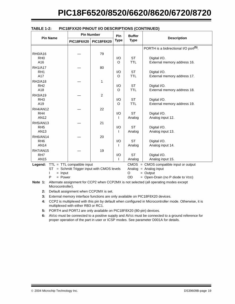
PORTH is a bidirectional I/O port(5).
RH0/A16RH0A16
— 79I/OO
STTTL
Digital I/O.External memory address 16.
RH1/A17RH1A17
— 80I/OO
STTTL
Digital I/O.External memory address 17.
RH2/A18RH2A18
— 1I/OO
STTTL
Digital I/O.External memory address 18.
RH3/A19RH3A19
— 2I/OO
STTTL
Digital I/O.External memory address 19.
RH4/AN12RH4AN12
— 22I/OI
STAnalog
Digital I/O.Analog input 12.
RH5/AN13RH5AN13
— 21I/OI
STAnalog
Digital I/O.Analog input 13.
RH6/AN14RH6AN14
— 20I/OI
STAnalog
Digital I/O.Analog input 14.
RH7/AN15RH7AN15
— 19I/OI
STAnalog
Digital I/O.Analog input 15.
TABLE 1-2: PIC18FXX20 PINOUT I/O DESCRIPTIONS (CONTINUED)
Pin NamePin Number Pin
TypeBufferType
DescriptionPIC18F6X20 PIC18F8X20
Legend: TTL = TTL compatible input CMOS = CMOS compatible input or output ST = Schmitt Trigger input with CMOS levels Analog = Analog input I = Input O = Output P = Power OD = Open-Drain (no P diode to VDD)
Note 1: Alternate assignment for CCP2 when CCP2MX is not selected (all operating modes except Microcontroller).
2: Default assignment when CCP2MX is set.
3: External memory interface functions are only available on PIC18F8X20 devices.4: CCP2 is multiplexed with this pin by default when configured in Microcontroller mode. Otherwise, it is
multiplexed with either RB3 or RC1.5: PORTH and PORTJ are only available on PIC18F8X20 (80-pin) devices.6: AVDD must be connected to a positive supply and AVSS must be connected to a ground reference for
proper operation of the part in user or ICSP modes. See parameter D001A for details.
2004 Microchip Technology Inc. DS39609B-page 19
PIC18F6520/8520/6620/8620/6720/8720
PORTJ is a bidirectional I/O port(5).
RJ0/ALERJ0ALE
— 62I/OO
STTTL
Digital I/O.External memory address latch enable.
RJ1/OERJ1OE
— 61I/OO
STTTL
Digital I/O.External memory output enable.
RJ2/WRLRJ2WRL
— 60I/OO
STTTL
Digital I/O.External memory write low control.
RJ3/WRHRJ3WRH
— 59I/OO
STTTL
Digital I/O.External memory write high control.
RJ4/BA0RJ4BA0
— 39I/OO
STTTL
Digital I/O.External memory Byte Address 0 control.
RJ5/CERJ5CE
— 40I/OO
STTTL
Digital I/O.External memory chip enable control.
RJ6/LBRJ6LB
— 41I/OO
STTTL
Digital I/O.External memory low byte select.
RJ7/UBRJ7UB
— 42I/OO
STTTL
Digital I/O.External memory high byte select.
VSS 9, 25, 41, 56
11, 31, 51, 70
P — Ground reference for logic and I/O pins.
VDD 10, 26, 38, 57
12, 32, 48, 71
P — Positive supply for logic and I/O pins.
AVSS(6) 20 26 P — Ground reference for analog modules.
AVDD(6) 19 25 P — Positive supply for analog modules.
TABLE 1-2: PIC18FXX20 PINOUT I/O DESCRIPTIONS (CONTINUED)
Pin NamePin Number Pin
TypeBufferType
DescriptionPIC18F6X20 PIC18F8X20
Legend: TTL = TTL compatible input CMOS = CMOS compatible input or output ST = Schmitt Trigger input with CMOS levels Analog = Analog input I = Input O = Output P = Power OD = Open-Drain (no P diode to VDD)
Note 1: Alternate assignment for CCP2 when CCP2MX is not selected (all operating modes except Microcontroller).
2: Default assignment when CCP2MX is set.3: External memory interface functions are only available on PIC18F8X20 devices.
4: CCP2 is multiplexed with this pin by default when configured in Microcontroller mode. Otherwise, it is multiplexed with either RB3 or RC1.
5: PORTH and PORTJ are only available on PIC18F8X20 (80-pin) devices.6: AVDD must be connected to a positive supply and AVSS must be connected to a ground reference for
proper operation of the part in user or ICSP modes. See parameter D001A for details.
DS39609B-page 20 2004 Microchip Technology Inc.

PIC18F6520/8520/6620/8620/6720/8720
2.0 OSCILLATOR CONFIGURATIONS
2.1 Oscillator Types
The PIC18FXX20 devices can be operated in eightdifferent oscillator modes. The user can program threeconfiguration bits (FOSC2, FOSC1 and FOSC0) toselect one of these eight modes:
1. LP Low-Power Crystal2. XT Crystal/Resonator3. HS High-Speed Crystal/Resonator
4. HS+PLL High-Speed Crystal/Resonator with PLL enabled
5. RC External Resistor/Capacitor6. RCIO External Resistor/Capacitor with
I/O pin enabled7. EC External Clock8. ECIO External Clock with I/O pin
enabled
2.2 Crystal Oscillator/Ceramic Resonators
In XT, LP, HS or HS+PLL Oscillator modes, a crystal orceramic resonator is connected to the OSC1 andOSC2 pins to establish oscillation. Figure 2-1 showsthe pin connections.
The PIC18FXX20 oscillator design requires the use ofa parallel cut crystal.
FIGURE 2-1: CRYSTAL/CERAMIC RESONATOR OPERATION (HS, XT OR LP CONFIGURATION)
TABLE 2-1: CAPACITOR SELECTION FOR CERAMIC RESONATORS
Note: Use of a series cut crystal may give a fre-quency out of the crystal manufacturer’sspecifications.
Note 1: See Table 2-1 and Table 2-2 for recommendedvalues of C1 and C2.
2: A series resistor (RS) may be required for ATstrip cut crystals.
3: RF varies with the oscillator mode chosen.
C1(1)
C2(1)
XTAL
OSC2
OSC1
RF(3)
Sleep
To
Logic
PIC18FXX20RS(2)
Internal
Ranges Tested:
Mode Freq C1 C2
XT 455 kHz2.0 MHz4.0 MHz
68-100 pF15-68 pF15-68 pF
68-100 pF15-68 pF15-68 pF
HS 8.0 MHz16.0 MHz
10-68 pF10-22 pF
10-68 pF10-22 pF
These values are for design guidance only. See notes following this table.
Resonators Used:
2.0 MHz Murata Erie CSA2.00MG ± 0.5%4.0 MHz Murata Erie CSA4.00MG ± 0.5%8.0 MHz Murata Erie CSA8.00MT ± 0.5%
16.0 MHz Murata Erie CSA16.00MX ± 0.5%All resonators used did not have built-in capacitors.
Note 1: Higher capacitance increases the stabilityof the oscillator, but also increases thestart-up time.
2: When operating below 3V VDD, or whenusing certain ceramic resonators at anyvoltage, it may be necessary to use highgain HS mode, try a lower frequencyresonator, or switch to a crystal oscillator.
3: Since each resonator/crystal has its owncharacteristics, the user should consultthe resonator/crystal manufacturer forappropriate values of externalcomponents, or verify oscillatorperformance.
2004 Microchip Technology Inc. DS39609B-page 21

PIC18F6520/8520/6620/8620/6720/8720
TABLE 2-2: CAPACITOR SELECTION FOR CRYSTAL OSCILLATOR
An external clock source may also be connected to theOSC1 pin in the HS, XT and LP modes, as shown inFigure 2-2.
FIGURE 2-2: EXTERNAL CLOCK INPUT OPERATION (HS, XT OR LP OSC CONFIGURATION)
2.3 RC Oscillator
For timing insensitive applications, the “RC” and“RCIO” device options offer additional cost savings.The RC oscillator frequency is a function of the supplyvoltage, the resistor (REXT) and capacitor (CEXT) val-ues and the operating temperature. In addition to this,the oscillator frequency will vary from unit to unit, dueto normal process parameter variation. Furthermore,the difference in lead frame capacitance between pack-age types will also affect the oscillation frequency,especially for low CEXT values. The user also needs totake into account variation due to tolerance of externalR and C components used. Figure 2-3 shows how theR/C combination is connected.
In the RC Oscillator mode, the oscillator frequencydivided by 4 is available on the OSC2 pin. This signalmay be used for test purposes or to synchronize otherlogic.
FIGURE 2-3: RC OSCILLATOR MODE
The RCIO Oscillator mode functions like the RC mode,except that the OSC2 pin becomes an additionalgeneral purpose I/O pin. The I/O pin becomes bit 6 ofPORTA (RA6).
Ranges Tested:
Mode Freq C1 C2
LP 32 kHz15-22 pF 15-22 pF
200 kHz
XT 1 MHz15-22 pF 15-22 pF
4 MHz
HS 4 MHz
15-22 pF 15-22 pF8 MHz
20 MHz
Capacitor values are for design guidance only.
These capacitors were tested with the above crystalfrequencies for basic start-up and operation. Thesevalues are not optimized.
Different capacitor values may be required to produceacceptable oscillator operation. The user should testthe performance of the oscillator over the expectedVDD and temperature range for the application.
See the notes following this table for additionalinformation.
Note 1: Higher capacitance increases the stabilityof the oscillator, but also increases thestart-up time.
2: When operating below 3V VDD, or whenusing certain ceramic resonators at anyvoltage, it may be necessary to use theHS mode or switch to a crystal oscillator.
3: Since each resonator/crystal has itsown characteristics, the user shouldconsult the resonator/crystal manufac-turer for appropriate values of externalcomponents, or verify oscillatorperformance.
4: RS may be required to avoid overdrivingcrystals with low drive level specification.
5: Always verify oscillator performance overthe VDD and temperature range that isexpected for the application.
OSC1
OSC2Open
Clock fromExt. System PIC18FXX20
OSC2/CLKO
CEXT
REXT
PIC18FXX20
OSC1
FOSC/4
InternalClock
VDD
VSS
Recommended values: 3 kΩ ≤ REXT ≤ 100 kΩ
CEXT > 20 pF
DS39609B-page 22 2004 Microchip Technology Inc.

PIC18F6520/8520/6620/8620/6720/8720
2.4 External Clock Input
The EC and ECIO Oscillator modes require an externalclock source to be connected to the OSC1 pin. Thefeedback device between OSC1 and OSC2 is turnedoff in these modes to save current. There is a maximum1.5 µs start-up required after a Power-on Reset, orwake-up from Sleep mode.
In the EC Oscillator mode, the oscillator frequencydivided by 4 is available on the OSC2 pin. This signalmay be used for test purposes or to synchronize otherlogic. Figure 2-4 shows the pin connections for the ECOscillator mode.
FIGURE 2-4: EXTERNAL CLOCK INPUT OPERATION (EC CONFIGURATION)
The ECIO Oscillator mode functions like the EC mode,except that the OSC2 pin becomes an additional gen-eral purpose I/O pin. The I/O pin becomes bit 6 ofPORTA (RA6). Figure 2-5 shows the pin connectionsfor the ECIO Oscillator mode.
FIGURE 2-5: EXTERNAL CLOCK INPUT OPERATION (ECIO CONFIGURATION)
2.5 HS/PLL
A Phase Locked Loop circuit (PLL) is provided as aprogrammable option for users that want to multiply thefrequency of the incoming crystal oscillator signal by 4.For an input clock frequency of 10 MHz, the internalclock frequency will be multiplied to 40 MHz. This isuseful for customers who are concerned with EMI dueto high-frequency crystals.
The PLL is one of the modes of the FOSC<2:0> config-uration bits. The oscillator mode is specified duringdevice programming.
The PLL can only be enabled when the oscillator con-figuration bits are programmed for HS mode. If they areprogrammed for any other mode, the PLL is notenabled and the system clock will come directly fromOSC1. Also, PLL operation cannot be changed “on-the-fly”. To enable or disable it, the controller musteither cycle through a Power-on Reset, or switch theclock source from the main oscillator to the Timer1oscillator and back again. See Section 2.6 “OscillatorSwitching Feature” for details on oscillator switching.
A PLL lock timer is used to ensure that the PLL haslocked before device execution starts. The PLL locktimer has a time-out that is called TPLL.
FIGURE 2-6: PLL BLOCK DIAGRAM
OSC1
OSC2FOSC/4
Clock fromExt. System PIC18FXX20
OSC1
I/O (OSC2)RA6
Clock fromExt. System PIC18FXX20
MU
X
VCOLoopFilter
Divide by 4
CrystalOsc
OSC2
OSC1
PLL Enable
FIN
FOUT
SYSCLK
PhaseComparator
(from Configuration HS Oscbit Register)
2004 Microchip Technology Inc. DS39609B-page 23

PIC18F6520/8520/6620/8620/6720/8720
2.6 Oscillator Switching Feature
The PIC18FXX20 devices include a feature that allowsthe system clock source to be switched from the mainoscillator to an alternate low-frequency clock source.For the PIC18FXX20 devices, this alternate clocksource is the Timer1 oscillator. If a low-frequencycrystal (32 kHz, for example) has been attached to theTimer1 oscillator pins and the Timer1 oscillator hasbeen enabled, the device can switch to a low-power
execution mode. Figure 2-7 shows a block diagram ofthe system clock sources. The clock switching featureis enabled by programming the Oscillator SwitchingEnable (OSCSEN) bit in Configuration Register 1H to a‘0’. Clock switching is disabled in an erased device.See Section 12.0 “Timer1 Module” for further detailsof the Timer1 oscillator. See Section 23.0 “SpecialFeatures of the CPU” for Configuration registerdetails.
FIGURE 2-7: DEVICE CLOCK SOURCES
PIC18FXX20
TOSC
4 x PLL
TT1P
TSCLK
ClockSource
MU
X
TOSC/4
Timer1 Oscillator
T1OSCENEnableOscillator
T1OSO
T1OSI
Clock Source Option for other Modules
OSC1
OSC2
Sleep
Main Oscillator
DS39609B-page 24 2004 Microchip Technology Inc.

PIC18F6520/8520/6620/8620/6720/8720
2.6.1 SYSTEM CLOCK SWITCH BIT
The system clock source switching is performed undersoftware control. The system clock switch bit, SCS(OSCCON<0>), controls the clock switching. When theSCS bit is ‘0’, the system clock source comes from themain oscillator that is selected by the FOSC configura-tion bits in Configuration Register 1H. When the SCSbit is set, the system clock source will come from theTimer1 oscillator. The SCS bit is cleared on all forms ofReset.
REGISTER 2-1: OSCCON REGISTER
Note: The Timer1 oscillator must be enabledand operating to switch the system clocksource. The Timer1 oscillator is enabledby setting the T1OSCEN bit in the Timer1Control register (T1CON). If the Timer1oscillator is not enabled, then any write tothe SCS bit will be ignored (SCS bit forcedcleared) and the main oscillator willcontinue to be the system clock source.
U-0 U-0 U-0 U-0 U-0 U-0 U-0 R/W-1
— — — — — — — SCSbit 7 bit 0
bit 7-1 Unimplemented: Read as ‘0’
bit 0 SCS: System Clock Switch bitWhen OSCSEN Configuration bit = 0 and T1OSCEN bit is set:1 = Switch to Timer1 oscillator/clock pin 0 = Use primary oscillator/clock input pin
When OSCSEN and T1OSCEN are in other states:Bit is forced clear.
Legend:
R = Readable bit W = Writable bit U = Unimplemented bit, read as ‘0’
- n = Value at POR ‘1’ = Bit is set ‘0’ = Bit is cleared x = Bit is unknown
2004 Microchip Technology Inc. DS39609B-page 25

PIC18F6520/8520/6620/8620/6720/8720
2.6.2 OSCILLATOR TRANSITIONS
PIC18FXX20 devices contain circuitry to prevent“glitches” when switching between oscillator sources.Essentially, the circuitry waits for eight rising edges ofthe clock source that the processor is switching to. Thisensures that the new clock source is stable and that itspulse width will not be less than the shortest pulsewidth of the two clock sources.
A timing diagram indicating the transition from the mainoscillator to the Timer1 oscillator is shown in Figure 2-8.The Timer1 oscillator is assumed to be running all thetime. After the SCS bit is set, the processor is frozen atthe next occurring Q1 cycle. After eight synchronizationcycles are counted from the Timer1 oscillator, operationresumes. No additional delays are required after thesynchronization cycles.
FIGURE 2-8: TIMING DIAGRAM FOR TRANSITION FROM OSC1 TO TIMER1 OSCILLATOR
The sequence of events that takes place when switch-ing from the Timer1 oscillator to the main oscillator willdepend on the mode of the main oscillator. In additionto eight clock cycles of the main oscillator, additionaldelays may take place.
If the main oscillator is configured for an externalcrystal (HS, XT, LP), then the transition will take placeafter an oscillator start-up time (TOST) has occurred. Atiming diagram, indicating the transition from theTimer1 oscillator to the main oscillator for HS, XT andLP modes, is shown in Figure 2-9.
FIGURE 2-9: TIMING FOR TRANSITION BETWEEN TIMER1 AND OSC1 (HS, XT, LP)
Q3Q2Q1Q4Q3Q2
OSC1
Internal
SCS(OSCCON<0>)Program PC + 2PC
Note 1: Delay on internal system clock is eight oscillator cycles for synchronization.
Q1
T1OSI
Q4 Q1
PC + 4
Q1
TSCS
Clock
Counter
System
Q2 Q3 Q4 Q1
TDLY
TT1P
TOSC
21 3 4 5 6 7 8
Q3Q3 Q4 Q1 Q2 Q3 Q4 Q1 Q2
OSC1
Internal
SCS(OSCCON<0>)
ProgramPC PC + 2
Note 1: TOST = 1024 TOSC (drawing not to scale).
T1OSI
System Clock
OSC2
TOST
Q1
PC + 6
TT1P
TOSC
TSCS
1 2 3 4 5 6 7 8
Counter
DS39609B-page 26 2004 Microchip Technology Inc.

PIC18F6520/8520/6620/8620/6720/8720
If the main oscillator is configured for HS-PLL mode, anoscillator start-up time (TOST), plus an additional PLLtime-out (TPLL), will occur. The PLL time-out is typically2 ms and allows the PLL to lock to the main oscillator
frequency. A timing diagram, indicating the transitionfrom the Timer1 oscillator to the main oscillator forHS-PLL mode, is shown in Figure 2-10.
FIGURE 2-10: TIMING FOR TRANSITION BETWEEN TIMER1 AND OSC1 (HS WITH PLL)
If the main oscillator is configured in the RC, RCIO, ECor ECIO modes, there is no oscillator start-up time-out.Operation will resume after eight cycles of the mainoscillator have been counted. A timing diagram,
indicating the transition from the Timer1 oscillator to themain oscillator for RC, RCIO, EC and ECIO modes, isshown in Figure 2-11.
FIGURE 2-11: TIMING FOR TRANSITION BETWEEN TIMER1 AND OSC1 (RC, EC)
Q4 Q1 Q1 Q2 Q3 Q4 Q1 Q2
OSC1
Internal System
SCS(OSCCON<0>)
Program Counter PC PC + 2
Note 1:TOST = 1024 TOSC (drawing not to scale).
T1OSI
Clock
TOST
Q3
PC + 4
TPLL
TOSC
TT1P
TSCS
Q4
OSC2
PLL ClockInput 1 2 3 4 5 6 7 8
Q3 Q4 Q1 Q1 Q2 Q3 Q4 Q1 Q2 Q3
OSC1
Internal System
SCS(OSCCON<0>)
ProgramPC PC + 2
Note 1:RC Oscillator mode assumed.
PC + 4
T1OSI
Clock
OSC2
Q4TT1P
TOSC
TSCS
1 2 3 4 5 6 7 8
Counter
2004 Microchip Technology Inc. DS39609B-page 27

PIC18F6520/8520/6620/8620/6720/8720
2.7 Effects of Sleep Mode on the On-Chip Oscillator
When the device executes a SLEEP instruction, the on-chip clocks and oscillator are turned off and the deviceis held at the beginning of an instruction cycle (Q1state). With the oscillator off, the OSC1 and OSC2signals will stop oscillating. Since all the transistorswitching currents have been removed, Sleep modeachieves the lowest current consumption of the device(only leakage currents). Enabling any on-chip featurethat will operate during Sleep will increase the currentconsumed during Sleep. The user can wake fromSleep through external Reset, Watchdog Timer Resetor through an interrupt.
2.8 Power-up Delays
Power up delays are controlled by two timers so that noexternal Reset circuitry is required for mostapplications. The delays ensure that the device is keptin Reset until the device power supply and clock arestable. For additional information on Reset operation,see Section 3.0 “Reset”.
The first timer is the Power-up Timer (PWRT), whichoptionally provides a fixed delay of 72 ms (nominal) onpower-up only (POR and BOR). The second timer isthe Oscillator Start-up Timer (OST), intended to keepthe chip in Reset until the crystal oscillator is stable.
With the PLL enabled (HS/PLL Oscillator mode), thetime-out sequence following a Power-on Reset is differ-ent from other oscillator modes. The time-out sequenceis as follows: First, the PWRT time-out is invoked aftera POR time delay has expired. Then, the OscillatorStart-up Timer (OST) is invoked. However, this is stillnot a sufficient amount of time to allow the PLL to lockat high frequencies. The PWRT timer is used to providean additional fixed 2 ms (nominal) time-out to allow thePLL ample time to lock to the incoming clock frequency.
TABLE 2-3: OSC1 AND OSC2 PIN STATES IN SLEEP MODE
OSC Mode OSC1 Pin OSC2 Pin
RC Floating, external resistor should pull high At logic low
RCIO Floating, external resistor should pull high Configured as PORTA, bit 6
ECIO Floating Configured as PORTA, bit 6
EC Floating At logic low
LP, XT and HS Feedback inverter disabled at quiescent voltage level
Feedback inverter disabled at quiescent voltage level
Note: See Table 3-1 in Section 3.0 “Reset” for time-outs due to Sleep and MCLR Reset.
DS39609B-page 28 2004 Microchip Technology Inc.

PIC18F6520/8520/6620/8620/6720/8720
3.0 RESET
The PIC18FXX20 devices differentiate betweenvarious kinds of Reset:
a) Power-on Reset (POR)
b) MCLR Reset during normal operationc) MCLR Reset during Sleep d) Watchdog Timer (WDT) Reset (during normal
operation)e) Programmable Brown-out Reset (PBOR)
f) RESET Instructiong) Stack Full Reseth) Stack Underflow Reset
Most registers are unaffected by a Reset. Their statusis unknown on POR and unchanged by all otherResets. The other registers are forced to a “Resetstate” on Power-on Reset, MCLR, WDT Reset, Brown-out Reset, MCLR Reset during Sleep and by theRESET instruction.
Most registers are not affected by a WDT wake-up,since this is viewed as the resumption of normaloperation. Status bits from the RCON register, RI, TO,PD, POR and BOR, are set or cleared differently indifferent Reset situations, as indicated in Table 3-2.These bits are used in software to determine the natureof the Reset. See Table 3-3 for a full description of theReset states of all registers.
A simplified block diagram of the On-Chip Reset Circuitis shown in Figure 3-1.
The Enhanced MCU devices have a MCLR noise filterin the MCLR Reset path. The filter will detect andignore small pulses. The MCLR pin is not driven low byany internal Resets, including the WDT.
FIGURE 3-1: SIMPLIFIED BLOCK DIAGRAM OF ON-CHIP RESET CIRCUIT
S
R Q
External Reset
MCLR
VDD
OSC1
WDTModule
VDD RiseDetect
OST/PWRT
On-chipRC OSC(1)
WDTTime-out
Power-on Reset
OST
10-bit Ripple Counter
PWRT
Chip_Reset
10-bit Ripple Counter
Reset
Enable OST(2)
Enable PWRT
Sleep
Note 1: This is a separate oscillator from the RC oscillator of the CLKI pin.
2: See Table 3-1 for time-out situations.
Brown-outReset
BOREN
RESET Instruction
StackPointer
Stack Full/Underflow Reset
2004 Microchip Technology Inc. DS39609B-page 29
PIC18F6520/8520/6620/8620/6720/8720
3.1 Power-on Reset (POR)
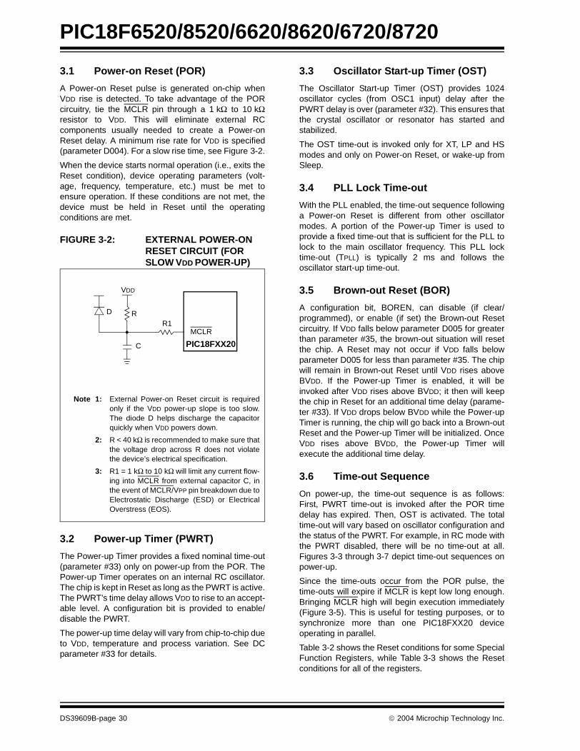
A Power-on Reset pulse is generated on-chip whenVDD rise is detected. To take advantage of the PORcircuitry, tie the MCLR pin through a 1 kΩ to 10 kΩresistor to VDD. This will eliminate external RCcomponents usually needed to create a Power-onReset delay. A minimum rise rate for VDD is specified(parameter D004). For a slow rise time, see Figure 3-2.
When the device starts normal operation (i.e., exits theReset condition), device operating parameters (volt-age, frequency, temperature, etc.) must be met toensure operation. If these conditions are not met, thedevice must be held in Reset until the operatingconditions are met.
FIGURE 3-2: EXTERNAL POWER-ON RESET CIRCUIT (FOR SLOW VDD POWER-UP)
3.2 Power-up Timer (PWRT)
The Power-up Timer provides a fixed nominal time-out(parameter #33) only on power-up from the POR. ThePower-up Timer operates on an internal RC oscillator.The chip is kept in Reset as long as the PWRT is active.The PWRT’s time delay allows VDD to rise to an accept-able level. A configuration bit is provided to enable/disable the PWRT.
The power-up time delay will vary from chip-to-chip dueto VDD, temperature and process variation. See DCparameter #33 for details.
3.3 Oscillator Start-up Timer (OST)
The Oscillator Start-up Timer (OST) provides 1024oscillator cycles (from OSC1 input) delay after thePWRT delay is over (parameter #32). This ensures thatthe crystal oscillator or resonator has started andstabilized.
The OST time-out is invoked only for XT, LP and HSmodes and only on Power-on Reset, or wake-up fromSleep.
3.4 PLL Lock Time-out
With the PLL enabled, the time-out sequence followinga Power-on Reset is different from other oscillatormodes. A portion of the Power-up Timer is used toprovide a fixed time-out that is sufficient for the PLL tolock to the main oscillator frequency. This PLL locktime-out (TPLL) is typically 2 ms and follows theoscillator start-up time-out.
3.5 Brown-out Reset (BOR)
A configuration bit, BOREN, can disable (if clear/programmed), or enable (if set) the Brown-out Resetcircuitry. If VDD falls below parameter D005 for greaterthan parameter #35, the brown-out situation will resetthe chip. A Reset may not occur if VDD falls belowparameter D005 for less than parameter #35. The chipwill remain in Brown-out Reset until VDD rises aboveBVDD. If the Power-up Timer is enabled, it will beinvoked after VDD rises above BVDD; it then will keepthe chip in Reset for an additional time delay (parame-ter #33). If VDD drops below BVDD while the Power-upTimer is running, the chip will go back into a Brown-outReset and the Power-up Timer will be initialized. OnceVDD rises above BVDD, the Power-up Timer willexecute the additional time delay.
3.6 Time-out Sequence
On power-up, the time-out sequence is as follows:First, PWRT time-out is invoked after the POR timedelay has expired. Then, OST is activated. The totaltime-out will vary based on oscillator configuration andthe status of the PWRT. For example, in RC mode withthe PWRT disabled, there will be no time-out at all.Figures 3-3 through 3-7 depict time-out sequences onpower-up.
Since the time-outs occur from the POR pulse, thetime-outs will expire if MCLR is kept low long enough.Bringing MCLR high will begin execution immediately(Figure 3-5). This is useful for testing purposes, or tosynchronize more than one PIC18FXX20 deviceoperating in parallel.
Table 3-2 shows the Reset conditions for some SpecialFunction Registers, while Table 3-3 shows the Resetconditions for all of the registers.
Note 1: External Power-on Reset circuit is requiredonly if the VDD power-up slope is too slow.The diode D helps discharge the capacitorquickly when VDD powers down.
2: R < 40 kΩ is recommended to make sure thatthe voltage drop across R does not violatethe device’s electrical specification.
3: R1 = 1 kΩ to 10 kΩ will limit any current flow-ing into MCLR from external capacitor C, inthe event of MCLR/VPP pin breakdown due toElectrostatic Discharge (ESD) or ElectricalOverstress (EOS).
C
R1RD
VDD
MCLR
PIC18FXX20
DS39609B-page 30 2004 Microchip Technology Inc.

PIC18F6520/8520/6620/8620/6720/8720
TABLE 3-1: TIME-OUT IN VARIOUS SITUATIONS
REGISTER 3-1: RCON REGISTER BITS AND POSITIONS
TABLE 3-2: STATUS BITS, THEIR SIGNIFICANCE AND THE INITIALIZATION CONDITION FOR RCON REGISTER
OscillatorConfiguration
Power-up(2)
Brown-out Wake-up from
Sleep orOscillator SwitchPWRTE = 0 PWRTE = 1
HS with PLL enabled(1) 72 ms + 1024 TOSC + 2ms
1024 TOSC + 2 ms
72 ms(2) + 1024 TOSC + 2 ms
1024 TOSC + 2 ms
HS, XT, LP 72 ms + 1024 TOSC 1024 TOSC 72 ms(2) + 1024 TOSC 1024 TOSC
EC 72 ms 1.5 µs 72 ms(2) 1.5 µs(3)
External RC 72 ms — 72 ms(2) —
Note 1: 2 ms is the nominal time required for the 4xPLL to lock.
2: 72 ms is the nominal power-up timer delay, if implemented.3: 1.5 µs is the recovery time from Sleep. There is no recovery time from oscillator switch.
R/W-0 U-0 U-0 R/W-1 R/W-1 R/W-1 R/W-1 R/W-1
IPEN — — RI TO PD POR BOR
bit 7 bit 0
Note 1: Refer to Section 4.14 “RCON Register” for bit definitions.
ConditionProgram Counter
RCONRegister
RI TO PD POR BOR STKFUL STKUNF
Power-on Reset 0000h 0--1 1100 1 1 1 0 0 u u
MCLR Reset during normal operation
0000h 0--u uuuu u u u u u u u
Software Reset during normal operation
0000h 0--0 uuuu 0 u u u u u u
Stack Full Reset during normal operation
0000h 0--u uu11 u u u u u u 1
Stack Underflow Reset during normal operation
0000h 0--u uu11 u u u u u 1 u
MCLR Reset during Sleep 0000h 0--u 10uu u 1 0 u u u u
WDT Reset 0000h 0--u 01uu 1 0 1 u u u u
WDT Wake-up PC + 2 u--u 00uu u 0 0 u u u u
Brown-out Reset 0000h 0--1 11u0 1 1 1 1 0 u u
Interrupt wake-up from Sleep PC + 2(1) u--u 00uu u 1 0 u u u u
Legend: u = unchanged, x = unknown, – = unimplemented bit, read as ‘0’Note 1: When the wake-up is due to an interrupt and the GIEH or GIEL bits are set, the PC is loaded with the
interrupt vector (0x000008h or 0x000018h).
2004 Microchip Technology Inc. DS39609B-page 31
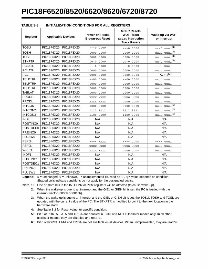
PIC18F6520/8520/6620/8620/6720/8720
TABLE 3-3: INITIALIZATION CONDITIONS FOR ALL REGISTERS
Register Applicable DevicesPower-on Reset,Brown-out Reset
MCLR ResetsWDT Reset
RESET InstructionStack Resets
Wake-up via WDT or Interrupt
TOSU PIC18F6X20 PIC18F8X20 ---0 0000 ---0 0000 ---0 uuuu(3)
TOSH PIC18F6X20 PIC18F8X20 0000 0000 0000 0000 uuuu uuuu(3)
TOSL PIC18F6X20 PIC18F8X20 0000 0000 0000 0000 uuuu uuuu(3)
STKPTR PIC18F6X20 PIC18F8X20 00-0 0000 uu-0 0000 uu-u uuuu(3)
PCLATU PIC18F6X20 PIC18F8X20 ---0 0000 ---0 0000 ---u uuuu
PCLATH PIC18F6X20 PIC18F8X20 0000 0000 0000 0000 uuuu uuuu
PCL PIC18F6X20 PIC18F8X20 0000 0000 0000 0000 PC + 2(2)
TBLPTRU PIC18F6X20 PIC18F8X20 --00 0000 --00 0000 --uu uuuu
TBLPTRH PIC18F6X20 PIC18F8X20 0000 0000 0000 0000 uuuu uuuu
TBLPTRL PIC18F6X20 PIC18F8X20 0000 0000 0000 0000 uuuu uuuu
TABLAT PIC18F6X20 PIC18F8X20 0000 0000 0000 0000 uuuu uuuu
PRODH PIC18F6X20 PIC18F8X20 xxxx xxxx uuuu uuuu uuuu uuuu
PRODL PIC18F6X20 PIC18F8X20 xxxx xxxx uuuu uuuu uuuu uuuu
INTCON PIC18F6X20 PIC18F8X20 0000 000x 0000 000u uuuu uuuu(1)
INTCON2 PIC18F6X20 PIC18F8X20 1111 1111 1111 1111 uuuu uuuu(1)
INTCON3 PIC18F6X20 PIC18F8X20 1100 0000 1100 0000 uuuu uuuu(1)
INDF0 PIC18F6X20 PIC18F8X20 N/A N/A N/APOSTINC0 PIC18F6X20 PIC18F8X20 N/A N/A N/APOSTDEC0 PIC18F6X20 PIC18F8X20 N/A N/A N/A
PREINC0 PIC18F6X20 PIC18F8X20 N/A N/A N/APLUSW0 PIC18F6X20 PIC18F8X20 N/A N/A N/AFSR0H PIC18F6X20 PIC18F8X20 ---- xxxx ---- uuuu ---- uuuu
FSR0L PIC18F6X20 PIC18F8X20 xxxx xxxx uuuu uuuu uuuu uuuu
WREG PIC18F6X20 PIC18F8X20 xxxx xxxx uuuu uuuu uuuu uuuu
INDF1 PIC18F6X20 PIC18F8X20 N/A N/A N/A
POSTINC1 PIC18F6X20 PIC18F8X20 N/A N/A N/APOSTDEC1 PIC18F6X20 PIC18F8X20 N/A N/A N/APREINC1 PIC18F6X20 PIC18F8X20 N/A N/A N/A
PLUSW1 PIC18F6X20 PIC18F8X20 N/A N/A N/ALegend: u = unchanged, x = unknown, - = unimplemented bit, read as ‘0’, q = value depends on condition.
Shaded cells indicate conditions do not apply for the designated device.Note 1: One or more bits in the INTCONx or PIRx registers will be affected (to cause wake-up).
2: When the wake-up is due to an interrupt and the GIEL or GIEH bit is set, the PC is loaded with the interrupt vector (0008h or 0018h).
3: When the wake-up is due to an interrupt and the GIEL or GIEH bit is set, the TOSU, TOSH and TOSL are updated with the current value of the PC. The STKPTR is modified to point to the next location in the hardware stack.
4: See Table 3-2 for Reset value for specific condition.5: Bit 6 of PORTA, LATA and TRISA are enabled in ECIO and RCIO Oscillator modes only. In all other
oscillator modes, they are disabled and read ‘0’. 6: Bit 6 of PORTA, LATA and TRISA are not available on all devices. When unimplemented, they are read ‘0’.
DS39609B-page 32 2004 Microchip Technology Inc.

PIC18F6520/8520/6620/8620/6720/8720
FSR1H PIC18F6X20 PIC18F8X20 ---- xxxx ---- uuuu ---- uuuu
FSR1L PIC18F6X20 PIC18F8X20 xxxx xxxx uuuu uuuu uuuu uuuu
BSR PIC18F6X20 PIC18F8X20 ---- 0000 ---- 0000 ---- uuuu
INDF2 PIC18F6X20 PIC18F8X20 N/A N/A N/APOSTINC2 PIC18F6X20 PIC18F8X20 N/A N/A N/APOSTDEC2 PIC18F6X20 PIC18F8X20 N/A N/A N/A
PREINC2 PIC18F6X20 PIC18F8X20 N/A N/A N/APLUSW2 PIC18F6X20 PIC18F8X20 N/A N/A N/AFSR2H PIC18F6X20 PIC18F8X20 ---- xxxx ---- uuuu ---- uuuu
FSR2L PIC18F6X20 PIC18F8X20 xxxx xxxx uuuu uuuu uuuu uuuu
STATUS PIC18F6X20 PIC18F8X20 ---x xxxx ---u uuuu ---u uuuu
TMR0H PIC18F6X20 PIC18F8X20 0000 0000 uuuu uuuu uuuu uuuu
TMR0L PIC18F6X20 PIC18F8X20 xxxx xxxx uuuu uuuu uuuu uuuu
T0CON PIC18F6X20 PIC18F8X20 1111 1111 1111 1111 uuuu uuuu
OSCCON PIC18F6X20 PIC18F8X20 ---- ---0 ---- ---0 ---- ---u
LVDCON PIC18F6X20 PIC18F8X20 --00 0101 --00 0101 --uu uuuu
WDTCON PIC18F6X20 PIC18F8X20 ---- ---0 ---- ---0 ---- ---u
RCON(4) PIC18F6X20 PIC18F8X20 0--q 11qq 0--q qquu u--u qquu
TMR1H PIC18F6X20 PIC18F8X20 xxxx xxxx uuuu uuuu uuuu uuuu
TMR1L PIC18F6X20 PIC18F8X20 xxxx xxxx uuuu uuuu uuuu uuuu
T1CON PIC18F6X20 PIC18F8X20 0-00 0000 u-uu uuuu u-uu uuuu
TMR2 PIC18F6X20 PIC18F8X20 0000 0000 0000 0000 uuuu uuuu
PR2 PIC18F6X20 PIC18F8X20 1111 1111 1111 1111 1111 1111
T2CON PIC18F6X20 PIC18F8X20 -000 0000 -000 0000 -uuu uuuu
SSPBUF PIC18F6X20 PIC18F8X20 xxxx xxxx uuuu uuuu uuuu uuuu
SSPADD PIC18F6X20 PIC18F8X20 0000 0000 0000 0000 uuuu uuuu
SSPSTAT PIC18F6X20 PIC18F8X20 0000 0000 0000 0000 uuuu uuuu
SSPCON1 PIC18F6X20 PIC18F8X20 0000 0000 0000 0000 uuuu uuuu
SSPCON2 PIC18F6X20 PIC18F8X20 0000 0000 0000 0000 uuuu uuuu
TABLE 3-3: INITIALIZATION CONDITIONS FOR ALL REGISTERS (CONTINUED)
Register Applicable DevicesPower-on Reset,Brown-out Reset
MCLR ResetsWDT Reset
RESET InstructionStack Resets
Wake-up via WDT or Interrupt
Legend: u = unchanged, x = unknown, - = unimplemented bit, read as ‘0’, q = value depends on condition.Shaded cells indicate conditions do not apply for the designated device.
Note 1: One or more bits in the INTCONx or PIRx registers will be affected (to cause wake-up).
2: When the wake-up is due to an interrupt and the GIEL or GIEH bit is set, the PC is loaded with the interrupt vector (0008h or 0018h).
3: When the wake-up is due to an interrupt and the GIEL or GIEH bit is set, the TOSU, TOSH and TOSL are updated with the current value of the PC. The STKPTR is modified to point to the next location in the hardware stack.
4: See Table 3-2 for Reset value for specific condition.
5: Bit 6 of PORTA, LATA and TRISA are enabled in ECIO and RCIO Oscillator modes only. In all other oscillator modes, they are disabled and read ‘0’.
6: Bit 6 of PORTA, LATA and TRISA are not available on all devices. When unimplemented, they are read ‘0’.
2004 Microchip Technology Inc. DS39609B-page 33

PIC18F6520/8520/6620/8620/6720/8720
ADRESH PIC18F6X20 PIC18F8X20 xxxx xxxx uuuu uuuu uuuu uuuu
ADRESL PIC18F6X20 PIC18F8X20 xxxx xxxx uuuu uuuu uuuu uuuu
ADCON0 PIC18F6X20 PIC18F8X20 --00 0000 --00 0000 --uu uuuu
ADCON1 PIC18F6X20 PIC18F8X20 --00 0000 --00 0000 --uu uuuu
ADCON2 PIC18F6X20 PIC18F8X20 0--- -000 0--- -000 u--- -uuu
CCPR1H PIC18F6X20 PIC18F8X20 xxxx xxxx uuuu uuuu uuuu uuuu
CCPR1L PIC18F6X20 PIC18F8X20 xxxx xxxx uuuu uuuu uuuu uuuu
CCP1CON PIC18F6X20 PIC18F8X20 --00 0000 --00 0000 --uu uuuu
CCPR2H PIC18F6X20 PIC18F8X20 xxxx xxxx uuuu uuuu uuuu uuuu
CCPR2L PIC18F6X20 PIC18F8X20 xxxx xxxx uuuu uuuu uuuu uuuu
CCP2CON PIC18F6X20 PIC18F8X20 --00 0000 --00 0000 --uu uuuu
CCPR3H PIC18F6X20 PIC18F8X20 xxxx xxxx uuuu uuuu uuuu uuuu
CCPR3L PIC18F6X20 PIC18F8X20 xxxx xxxx uuuu uuuu uuuu uuuu
CCP3CON PIC18F6X20 PIC18F8X20 0000 0000 0000 0000 uuuu uuuu
CVRCON PIC18F6X20 PIC18F8X20 0000 0000 0000 0000 uuuu uuuu
CMCON PIC18F6X20 PIC18F8X20 0000 0000 0000 0000 uuuu uuuu
TMR3H PIC18F6X20 PIC18F8X20 xxxx xxxx uuuu uuuu uuuu uuuu
TMR3L PIC18F6X20 PIC18F8X20 xxxx xxxx uuuu uuuu uuuu uuuu
T3CON PIC18F6X20 PIC18F8X20 0000 0000 uuuu uuuu uuuu uuuu
PSPCON PIC18F6X20 PIC18F8X20 0000 ---- 0000 ---- uuuu ----
SPBRG1 PIC18F6X20 PIC18F8X20 0000 0000 0000 0000 uuuu uuuu
RCREG1 PIC18F6X20 PIC18F8X20 0000 0000 0000 0000 uuuu uuuu
TXREG1 PIC18F6X20 PIC18F8X20 0000 0000 0000 0000 uuuu uuuu
TXSTA1 PIC18F6X20 PIC18F8X20 0000 -010 0000 -010 uuuu -uuu
RCSTA1 PIC18F6X20 PIC18F8X20 0000 000x 0000 000x uuuu uuuu
EEADRH PIC18F6X20 PIC18F8X20 ---- --00 ---- --00 ---- --uu
EEADR PIC18F6X20 PIC18F8X20 0000 0000 0000 0000 uuuu uuuu
EEDATA PIC18F6X20 PIC18F8X20 0000 0000 0000 0000 uuuu uuuu
EECON2 PIC18F6X20 PIC18F8X20 ---- ---- ---- ---- ---- ----
EECON1 PIC18F6X20 PIC18F8X20 xx-0 x000 uu-0 u000 uu-0 u000
TABLE 3-3: INITIALIZATION CONDITIONS FOR ALL REGISTERS (CONTINUED)
Register Applicable DevicesPower-on Reset,Brown-out Reset
MCLR ResetsWDT Reset
RESET InstructionStack Resets
Wake-up via WDT or Interrupt
Legend: u = unchanged, x = unknown, - = unimplemented bit, read as ‘0’, q = value depends on condition.Shaded cells indicate conditions do not apply for the designated device.
Note 1: One or more bits in the INTCONx or PIRx registers will be affected (to cause wake-up).2: When the wake-up is due to an interrupt and the GIEL or GIEH bit is set, the PC is loaded with the
interrupt vector (0008h or 0018h).3: When the wake-up is due to an interrupt and the GIEL or GIEH bit is set, the TOSU, TOSH and TOSL are
updated with the current value of the PC. The STKPTR is modified to point to the next location in the hardware stack.
4: See Table 3-2 for Reset value for specific condition.5: Bit 6 of PORTA, LATA and TRISA are enabled in ECIO and RCIO Oscillator modes only. In all other
oscillator modes, they are disabled and read ‘0’. 6: Bit 6 of PORTA, LATA and TRISA are not available on all devices. When unimplemented, they are read ‘0’.
DS39609B-page 34 2004 Microchip Technology Inc.
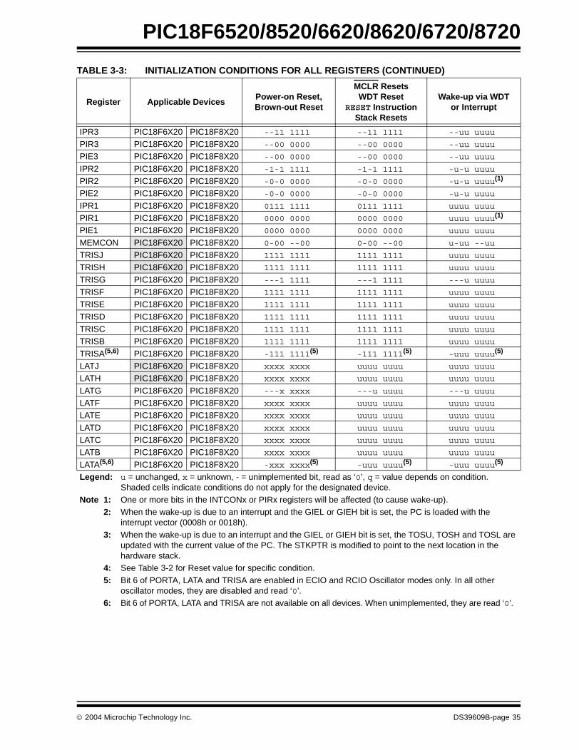
PIC18F6520/8520/6620/8620/6720/8720
IPR3 PIC18F6X20 PIC18F8X20 --11 1111 --11 1111 --uu uuuu
PIR3 PIC18F6X20 PIC18F8X20 --00 0000 --00 0000 --uu uuuu
PIE3 PIC18F6X20 PIC18F8X20 --00 0000 --00 0000 --uu uuuu
IPR2 PIC18F6X20 PIC18F8X20 -1-1 1111 -1-1 1111 -u-u uuuu
PIR2 PIC18F6X20 PIC18F8X20 -0-0 0000 -0-0 0000 -u-u uuuu(1)
PIE2 PIC18F6X20 PIC18F8X20 -0-0 0000 -0-0 0000 -u-u uuuu
IPR1 PIC18F6X20 PIC18F8X20 0111 1111 0111 1111 uuuu uuuu
PIR1 PIC18F6X20 PIC18F8X20 0000 0000 0000 0000 uuuu uuuu(1)
PIE1 PIC18F6X20 PIC18F8X20 0000 0000 0000 0000 uuuu uuuu
MEMCON PIC18F6X20 PIC18F8X20 0-00 --00 0-00 --00 u-uu --uu
TRISJ PIC18F6X20 PIC18F8X20 1111 1111 1111 1111 uuuu uuuu
TRISH PIC18F6X20 PIC18F8X20 1111 1111 1111 1111 uuuu uuuu
TRISG PIC18F6X20 PIC18F8X20 ---1 1111 ---1 1111 ---u uuuu
TRISF PIC18F6X20 PIC18F8X20 1111 1111 1111 1111 uuuu uuuu
TRISE PIC18F6X20 PIC18F8X20 1111 1111 1111 1111 uuuu uuuu
TRISD PIC18F6X20 PIC18F8X20 1111 1111 1111 1111 uuuu uuuu
TRISC PIC18F6X20 PIC18F8X20 1111 1111 1111 1111 uuuu uuuu
TRISB PIC18F6X20 PIC18F8X20 1111 1111 1111 1111 uuuu uuuu
TRISA(5,6) PIC18F6X20 PIC18F8X20 -111 1111(5) -111 1111(5) -uuu uuuu(5)
LATJ PIC18F6X20 PIC18F8X20 xxxx xxxx uuuu uuuu uuuu uuuu
LATH PIC18F6X20 PIC18F8X20 xxxx xxxx uuuu uuuu uuuu uuuu
LATG PIC18F6X20 PIC18F8X20 ---x xxxx ---u uuuu ---u uuuu
LATF PIC18F6X20 PIC18F8X20 xxxx xxxx uuuu uuuu uuuu uuuu
LATE PIC18F6X20 PIC18F8X20 xxxx xxxx uuuu uuuu uuuu uuuu
LATD PIC18F6X20 PIC18F8X20 xxxx xxxx uuuu uuuu uuuu uuuu
LATC PIC18F6X20 PIC18F8X20 xxxx xxxx uuuu uuuu uuuu uuuu
LATB PIC18F6X20 PIC18F8X20 xxxx xxxx uuuu uuuu uuuu uuuu
LATA(5,6) PIC18F6X20 PIC18F8X20 -xxx xxxx(5) -uuu uuuu(5) -uuu uuuu(5)
TABLE 3-3: INITIALIZATION CONDITIONS FOR ALL REGISTERS (CONTINUED)
Register Applicable DevicesPower-on Reset,Brown-out Reset
MCLR ResetsWDT Reset
RESET InstructionStack Resets
Wake-up via WDT or Interrupt
Legend: u = unchanged, x = unknown, - = unimplemented bit, read as ‘0’, q = value depends on condition.Shaded cells indicate conditions do not apply for the designated device.
Note 1: One or more bits in the INTCONx or PIRx registers will be affected (to cause wake-up).2: When the wake-up is due to an interrupt and the GIEL or GIEH bit is set, the PC is loaded with the
interrupt vector (0008h or 0018h).3: When the wake-up is due to an interrupt and the GIEL or GIEH bit is set, the TOSU, TOSH and TOSL are
updated with the current value of the PC. The STKPTR is modified to point to the next location in the hardware stack.
4: See Table 3-2 for Reset value for specific condition.5: Bit 6 of PORTA, LATA and TRISA are enabled in ECIO and RCIO Oscillator modes only. In all other
oscillator modes, they are disabled and read ‘0’. 6: Bit 6 of PORTA, LATA and TRISA are not available on all devices. When unimplemented, they are read ‘0’.
2004 Microchip Technology Inc. DS39609B-page 35
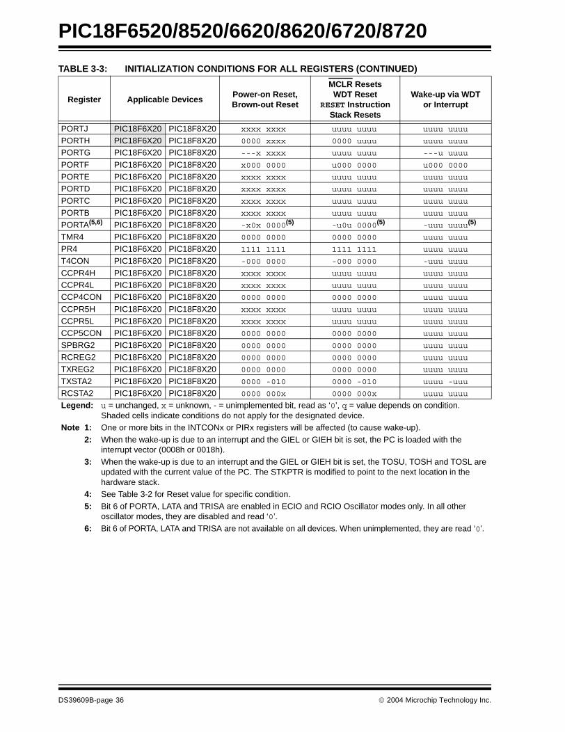
PIC18F6520/8520/6620/8620/6720/8720
PORTJ PIC18F6X20 PIC18F8X20 xxxx xxxx uuuu uuuu uuuu uuuu
PORTH PIC18F6X20 PIC18F8X20 0000 xxxx 0000 uuuu uuuu uuuu
PORTG PIC18F6X20 PIC18F8X20 ---x xxxx uuuu uuuu ---u uuuu
PORTF PIC18F6X20 PIC18F8X20 x000 0000 u000 0000 u000 0000
PORTE PIC18F6X20 PIC18F8X20 xxxx xxxx uuuu uuuu uuuu uuuu
PORTD PIC18F6X20 PIC18F8X20 xxxx xxxx uuuu uuuu uuuu uuuu
PORTC PIC18F6X20 PIC18F8X20 xxxx xxxx uuuu uuuu uuuu uuuu
PORTB PIC18F6X20 PIC18F8X20 xxxx xxxx uuuu uuuu uuuu uuuu
PORTA(5,6) PIC18F6X20 PIC18F8X20 -x0x 0000(5) -u0u 0000(5) -uuu uuuu(5)
TMR4 PIC18F6X20 PIC18F8X20 0000 0000 0000 0000 uuuu uuuu
PR4 PIC18F6X20 PIC18F8X20 1111 1111 1111 1111 uuuu uuuu
T4CON PIC18F6X20 PIC18F8X20 -000 0000 -000 0000 -uuu uuuu
CCPR4H PIC18F6X20 PIC18F8X20 xxxx xxxx uuuu uuuu uuuu uuuu
CCPR4L PIC18F6X20 PIC18F8X20 xxxx xxxx uuuu uuuu uuuu uuuu
CCP4CON PIC18F6X20 PIC18F8X20 0000 0000 0000 0000 uuuu uuuu
CCPR5H PIC18F6X20 PIC18F8X20 xxxx xxxx uuuu uuuu uuuu uuuu
CCPR5L PIC18F6X20 PIC18F8X20 xxxx xxxx uuuu uuuu uuuu uuuu
CCP5CON PIC18F6X20 PIC18F8X20 0000 0000 0000 0000 uuuu uuuu
SPBRG2 PIC18F6X20 PIC18F8X20 0000 0000 0000 0000 uuuu uuuu
RCREG2 PIC18F6X20 PIC18F8X20 0000 0000 0000 0000 uuuu uuuu
TXREG2 PIC18F6X20 PIC18F8X20 0000 0000 0000 0000 uuuu uuuu
TXSTA2 PIC18F6X20 PIC18F8X20 0000 -010 0000 -010 uuuu -uuu
RCSTA2 PIC18F6X20 PIC18F8X20 0000 000x 0000 000x uuuu uuuu
TABLE 3-3: INITIALIZATION CONDITIONS FOR ALL REGISTERS (CONTINUED)
Register Applicable DevicesPower-on Reset,Brown-out Reset
MCLR ResetsWDT Reset
RESET InstructionStack Resets
Wake-up via WDT or Interrupt
Legend: u = unchanged, x = unknown, - = unimplemented bit, read as ‘0’, q = value depends on condition.Shaded cells indicate conditions do not apply for the designated device.
Note 1: One or more bits in the INTCONx or PIRx registers will be affected (to cause wake-up).
2: When the wake-up is due to an interrupt and the GIEL or GIEH bit is set, the PC is loaded with the interrupt vector (0008h or 0018h).
3: When the wake-up is due to an interrupt and the GIEL or GIEH bit is set, the TOSU, TOSH and TOSL are updated with the current value of the PC. The STKPTR is modified to point to the next location in the hardware stack.
4: See Table 3-2 for Reset value for specific condition.
5: Bit 6 of PORTA, LATA and TRISA are enabled in ECIO and RCIO Oscillator modes only. In all other oscillator modes, they are disabled and read ‘0’.
6: Bit 6 of PORTA, LATA and TRISA are not available on all devices. When unimplemented, they are read ‘0’.
DS39609B-page 36 2004 Microchip Technology Inc.

PIC18F6520/8520/6620/8620/6720/8720
FIGURE 3-3: TIME-OUT SEQUENCE ON POWER-UP (MCLR TIED TO VDD VIA 1 kΩ RESISTOR)
FIGURE 3-4: TIME-OUT SEQUENCE ON POWER-UP (MCLR NOT TIED TO VDD): CASE 1
FIGURE 3-5: TIME-OUT SEQUENCE ON POWER-UP (MCLR NOT TIED TO VDD): CASE 2
TPWRT
TOST
VDD
MCLR
INTERNAL POR
PWRT TIME-OUT
OST TIME-OUT
INTERNAL RESET
TPWRT
TOST
VDD
MCLR
INTERNAL POR
PWRT TIME-OUT
OST TIME-OUT
INTERNAL RESET
VDD
MCLR
INTERNAL POR
PWRT TIME-OUT
OST TIME-OUT
INTERNAL RESET
TPWRT
TOST
2004 Microchip Technology Inc. DS39609B-page 37
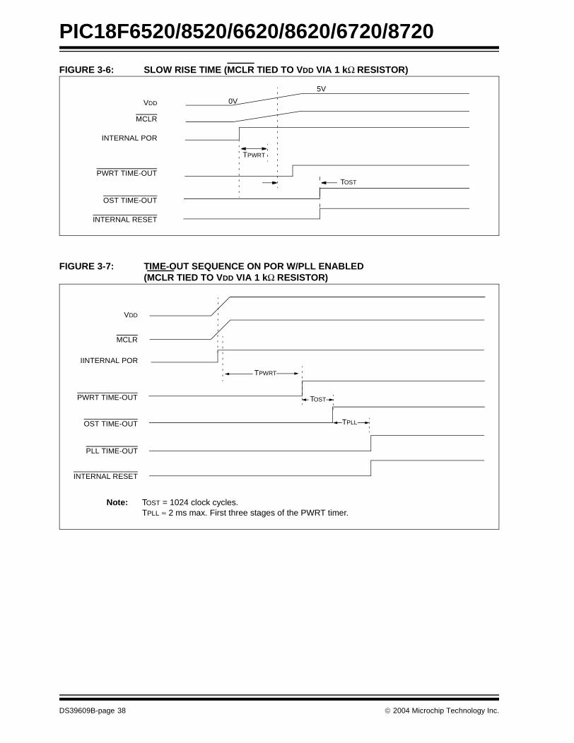
PIC18F6520/8520/6620/8620/6720/8720
FIGURE 3-6: SLOW RISE TIME (MCLR TIED TO VDD VIA 1 kΩ RESISTOR)
FIGURE 3-7: TIME-OUT SEQUENCE ON POR W/PLL ENABLED (MCLR TIED TO VDD VIA 1 kΩ RESISTOR)
VDD
MCLR
INTERNAL POR
PWRT TIME-OUT
OST TIME-OUT
INTERNAL RESET
0V
5V
TPWRT
TOST
TPWRT
TOST
VDD
MCLR
IINTERNAL POR
PWRT TIME-OUT
OST TIME-OUT
INTERNAL RESET
PLL TIME-OUT
TPLL
Note: TOST = 1024 clock cycles.TPLL ≈ 2 ms max. First three stages of the PWRT timer.
DS39609B-page 38 2004 Microchip Technology Inc.

PIC18F6520/8520/6620/8620/6720/8720
4.0 MEMORY ORGANIZATION
There are three memory blocks in PIC18FXX20devices. They are:
• Program Memory
• Data RAM• Data EEPROM
Data and program memory use separate busses,which allows for concurrent access of these blocks.Additional detailed information for Flash programmemory and data EEPROM is provided in Section 5.0“Flash Program Memory” and Section 7.0 “DataEEPROM Memory”, respectively.
In addition to on-chip Flash, the PIC18F8X20 devicesare also capable of accessing external program mem-ory through an external memory bus. Depending on theselected operating mode (discussed in Section 4.1.1“PIC18F8X20 Program Memory Modes”), the con-trollers may access either internal or external programmemory exclusively, or both internal and external mem-ory in selected blocks. Additional information on theExternal Memory Interface is provided in Section 6.0“External Memory Interface”.
4.1 Program Memory Organization
A 21-bit program counter is capable of addressing the2-Mbyte program memory space. Accessing a locationbetween the physically implemented memory and the2-Mbyte address will cause a read of all ‘0’s (a NOPinstruction).
Devices in the PIC18FXX20 family can be divided intothree groups, based on program memory size. ThePIC18FX520 devices (PIC18F6520 and PIC18F8520)have 32 Kbytes of on-chip Flash memory, equivalent to16,384 single-word instructions. The PIC18FX620devices (PIC18F6620 and PIC18F8620) have64 Kbytes of on-chip Flash memory, equivalent to32,768 single-word instructions. Finally, thePIC18FX720 devices (PIC18F6720 and PIC18F8720)have 128 Kbytes of on-chip Flash memory, equivalentto 65,536 single-word instructions.
For all devices, the Reset vector address is at 0000hand the interrupt vector addresses are at 0008h and0018h.
The program memory maps for all of the PIC18FXX20devices are compared in Figure 4-1.
4.1.1 PIC18F8X20 PROGRAM MEMORY MODES
PIC18F8X20 devices differ significantly from theirPIC18 predecessors in their utilization of programmemory. In addition to available on-chip Flash programmemory, these controllers can also address up to2 Mbytes of external program memory through theExternal Memory Interface. There are four distinctoperating modes available to the controllers:
• Microprocessor (MP)
• Microprocessor with Boot Block (MPBB)• Extended Microcontroller (EMC)• Microcontroller (MC)
The Program Memory mode is determined by settingthe two Least Significant bits of the CONFIG3L config-uration byte, as shown in Register 4-1. (See alsoSection 23.1 “Configuration Bits” for additionaldetails on the device configuration bits.)
The Program Memory modes operate as follows:
• The Microprocessor Mode permits access only to external program memory; the contents of the on-chip Flash memory are ignored. The 21-bit program counter permits access to a 2-Mbyte linear program memory space.
• The Microprocessor with Boot Block Mode accesses on-chip Flash memory from addresses 000000h to 0007FFh for PIC18F8520 devices and from 000000h to 0001FFh for PIC18F8620 and PIC18F8720 devices. Above this, external program memory is accessed all the way up to the 2-Mbyte limit. Program execution automati-cally switches between the two memories, as required.
• The Microcontroller Mode accesses only on-chip Flash memory. Attempts to read above the physical limit of the on-chip Flash (7FFFh for the PIC18F8520, 0FFFFh for the PIC18F8620, 1FFFFh for the PIC18F8720) causes a read of all ‘0’s (a NOP instruction). The Microcontroller mode is also the only operating mode available to PIC18F6X20 devices.
• The Extended Microcontroller Mode allows access to both internal and external program memories as a single block. The device can access its entire on-chip Flash memory; above this, the device accesses external program memory up to the 2-Mbyte program space limit. As with Boot Block mode, execution automatically switches between the two memories, as required.
In all modes, the microcontroller has complete accessto data RAM and EEPROM.
Figure 4-2 compares the memory maps of the differentProgram Memory modes. The differences between on-chip and external memory access limitations are morefully explained in Table 4-1.
2004 Microchip Technology Inc. DS39609B-page 39

PIC18F6520/8520/6620/8620/6720/8720
FIGURE 4-1: INTERNAL PROGRAM MEMORY MAP AND STACK FOR PIC18FXX20 DEVICES
TABLE 4-1: MEMORY ACCESS FOR PIC18F8X20 PROGRAM MEMORY MODES
PC<20:0>
Stack Level 1•
Stack Level 31
Reset Vector
Low Priority
••
CALL,RCALL,RETURNRETFIE,RETLW
21
On-Chip FlashProgram Memory
High Priority
Use
r M
emor
y S
pace
1FFFFFh
010000h00FFFFh
200000h
On-Chip FlashProgram Memory
On-Chip FlashProgram Memory
Read ‘0’ Read ‘0’ Read ‘0’
008000h007FFFh
020000h01FFFFh
000000h
000018h
000008h
1FFFFFh200000h
1FFFFFh200000h
PIC18FX520 PIC18FX620 PIC18FX720
Interrupt Vector
Interrupt Vector
000000h
000018h
000008h
000000h
000018h
000008h
Note: Size of memory regions not to scale.
(32 Kbyte) (64 Kbyte) (128 Kbyte)
Operating Mode
Internal Program Memory External Program Memory
ExecutionFrom
Table Read From
Table Write ToExecution
FromTable Read
FromTable Write To
Microprocessor No Access No Access No Access Yes Yes Yes
Microprocessor with Boot Block
Yes Yes Yes Yes Yes Yes
Microcontroller Yes Yes Yes No Access No Access No Access
Extended Microcontroller
Yes Yes Yes Yes Yes Yes
DS39609B-page 40 2004 Microchip Technology Inc.

PIC18F6520/8520/6620/8620/6720/8720
REGISTER 4-1: CONFIG3L CONFIGURATION BYTE
FIGURE 4-2: MEMORY MAPS FOR PIC18F8X20 PROGRAM MEMORY MODES
R/P-1 U-0 U-0 U-0 U-0 U-0 R/P-1 R/P-1
WAIT — — — — — PM1 PM0
bit 7 bit 0
bit 7 WAIT: External Bus Data Wait Enable bit1 = Wait selections unavailable, device will not wait 0 = Wait programmed by WAIT1 and WAIT0 bits of MEMCOM register (MEMCOM<5:4>)
bit 6-2 Unimplemented: Read as ‘0’
bit 1-0 PM1:PM0: Processor Data Memory Mode Select bits11 = Microcontroller mode10 = Microprocessor mode01 = Microcontroller with Boot Block mode 00 = Extended Microcontroller mode
Legend:
R = Readable bit P = Programmable bit U = Unimplemented bit, read as ‘0’
- n = Value after erase ‘1’ = Bit is set ‘0’ = Bit is cleared x = Bit is unknown
MicroprocessorMode (MP)
000000h
1FFFFFh
ExternalProgramMemory
ExternalProgramMemory
1FFFFFh
000000h
On-ChipProgramMemory
ExtendedMicrocontroller
Mode (EMC)
MicrocontrollerMode (MC)
000000h
External On-Chip
Pro
gra
m S
pace
Exe
cuti
on
On-ChipProgramMemory
1FFFFFh
Reads
Boot+1
1FFFFFh
Boot
Microprocessorwith Boot BlockMode (MPBB)
000000hOn-ChipProgramMemory
ExternalProgramMemory
Memory Flash
On-ChipProgramMemory
(Noaccess)
‘0’s
External On-ChipMemory Flash
On-ChipFlash
External On-ChipMemory Flash
Boundary Values for Microprocessor with Boot Block, Microcontroller and Extended Microcontroller modes(1)
Note 1: PIC18F6X20 devices are included here for completeness, to show the boundaries of their Boot Blocks and program memory spaces.
Device Boot Boot+1 Boundary Boundary+1 Available Memory Mode(s)
PIC18F6520 0007FFh 000800h 007FFFh 008000h MC
PIC18F6620 0001FFh 000200h 00FFFFh 010000h MC
PIC18F6720 0001FFh 000200h 01FFFFh 020000h MC
PIC18F8520 0007FFh 000800h 007FFFh 008000h MP, MPBB, MC, EMC
PIC18F8620 0001FFh 000200h 00FFFFh 010000h MP, MPBB, MC, EMC
PIC18F8720 0001FFh 000200h 01FFFFh 020000h MP, MPBB, MC, EMC
BoundaryBoundary+1
BoundaryBoundary+1
2004 Microchip Technology Inc. DS39609B-page 41

PIC18F6520/8520/6620/8620/6720/8720
4.2 Return Address Stack
The return address stack allows any combination of upto 31 program calls and interrupts to occur. The PC(Program Counter) is pushed onto the stack when aCALL or RCALL instruction is executed, or an interruptis Acknowledged. The PC value is pulled off the stackon a RETURN, RETLW or a RETFIE instruction. PCLATUand PCLATH are not affected by any of the RETURN orCALL instructions.
The stack operates as a 31-word by 21-bit RAM and a5-bit stack pointer, with the stack pointer initialized to00000b after all Resets. There is no RAM associatedwith stack pointer 00000b. This is only a Reset value.During a CALL type instruction, causing a push onto thestack, the stack pointer is first incremented and theRAM location pointed to by the stack pointer is writtenwith the contents of the PC. During a RETURN typeinstruction, causing a pop from the stack, the contentsof the RAM location pointed to by the STKPTR aretransferred to the PC and then the stack pointer isdecremented.
The stack space is not part of either program or dataspace. The stack pointer is readable and writable andthe address on the top of the stack is readable and writ-able through SFR registers. Data can also be pushedto, or popped from the stack using the top-of-stackSFRs. Status bits indicate if the stack pointer is at, orbeyond the 31 levels provided.
4.2.1 TOP-OF-STACK ACCESS
The top of the stack is readable and writable. Threeregister locations, TOSU, TOSH and TOSL, hold thecontents of the stack location pointed to by theSTKPTR register. This allows users to implement asoftware stack if necessary. After a CALL, RCALL orinterrupt, the software can read the pushed value byreading the TOSU, TOSH and TOSL registers. Thesevalues can be placed on a user defined software stack.At return time, the software can replace the TOSU,TOSH and TOSL and do a return.
The user must disable the global interrupt enable bitsduring this time to prevent inadvertent stackoperations.
4.2.2 RETURN STACK POINTER (STKPTR)
The STKPTR register contains the stack pointer value,the STKFUL (Stack Full) status bit and the STKUNF(Stack Underflow) status bits. Register 4-2 shows theSTKPTR register. The value of the stack pointer can be0 through 31. The stack pointer increments when val-ues are pushed onto the stack and decrements whenvalues are popped off the stack. At Reset, the stackpointer value will be ‘0’. The user may read and writethe stack pointer value. This feature can be used by aReal-Time Operating System for return stackmaintenance.
After the PC is pushed onto the stack 31 times (withoutpopping any values off the stack), the STKFUL bit isset. The STKFUL bit can only be cleared in software orby a POR.
The action that takes place when the stack becomesfull, depends on the state of the STVREN (Stack Over-flow Reset Enable) configuration bit. Refer toSection 24.0 “Instruction Set Summary” for adescription of the device configuration bits. If STVRENis set (default), the 31st push will push the (PC + 2)value onto the stack, set the STKFUL bit and reset thedevice. The STKFUL bit will remain set and the stackpointer will be set to ‘0’.
If STVREN is cleared, the STKFUL bit will be set on the31st push and the stack pointer will increment to 31.Any additional pushes will not overwrite the 31st pushand STKPTR will remain at 31.
When the stack has been popped enough times tounload the stack, the next pop will return a value of zeroto the PC and sets the STKUNF bit, while the stackpointer remains at ‘0’. The STKUNF bit will remain setuntil cleared in software or a POR occurs.
Note: Returning a value of zero to the PC on anunderflow has the effect of vectoring theprogram to the Reset vector, where thestack conditions can be verified andappropriate actions can be taken.
DS39609B-page 42 2004 Microchip Technology Inc.

PIC18F6520/8520/6620/8620/6720/8720
REGISTER 4-2: STKPTR REGISTER
FIGURE 4-3: RETURN ADDRESS STACK AND ASSOCIATED REGISTERS
4.2.3 PUSH AND POP INSTRUCTIONS
Since the Top-of-Stack (TOS) is readable and writable,the ability to push values onto the stack and pull valuesoff the stack, without disturbing normal programexecution, is a desirable option. To push the current PCvalue onto the stack, a PUSH instruction can beexecuted. This will increment the stack pointer and loadthe current PC value onto the stack. TOSU, TOSH andTOSL can then be modified to place a return addresson the stack.
The ability to pull the TOS value off of the stack andreplace it with the value that was previously pushedonto the stack, without disturbing normal execution, isachieved by using the POP instruction. The POPinstruction discards the current TOS by decrementingthe stack pointer. The previous value pushed onto thestack then becomes the TOS value.
4.2.4 STACK FULL/UNDERFLOW RESETS
These Resets are enabled by programming theSTVREN configuration bit. When the STVREN bit isdisabled, a full or underflow condition will set theappropriate STKFUL or STKUNF bit, but not cause adevice Reset. When the STVREN bit is enabled, a fullor underflow condition will set the appropriate STKFULor STKUNF bit and then cause a device Reset. TheSTKFUL or STKUNF bits are only cleared by the usersoftware or a POR Reset.
R/C-0 R/C-0 U-0 R/W-0 R/W-0 R/W-0 R/W-0 R/W-0
STKFUL(1) STKUNF(1) — SP4 SP3 SP2 SP1 SP0
bit 7 bit 0
bit 7 STKFUL: Stack Full Flag bit1 = Stack became full or overflowed 0 = Stack has not become full or overflowed
bit 6 STKUNF: Stack Underflow Flag bit
1 = Stack underflow occurred 0 = Stack underflow did not occur
bit 5 Unimplemented: Read as ‘0’
bit 4-0 SP4:SP0: Stack Pointer Location bits
Note 1: Bit 7 and bit 6 can only be cleared in user software or by a POR.
Legend:
R = Readable bit W = Writable bit U = Unimplemented bit, read as ‘0’
- n = Value at POR ‘1’ = Bit is set ‘0’ = Bit is cleared x = Bit is unknown
000110x001A34
111111111011101
000100000100000
00010
Return Address Stack
Top-of-Stack0x000D58
TOSLTOSHTOSU0x340x1A0x00
STKPTR<4:0>
2004 Microchip Technology Inc. DS39609B-page 43

PIC18F6520/8520/6620/8620/6720/8720
4.3 Fast Register Stack
A “fast interrupt return” option is available for interrupts.A Fast Register Stack is provided for the Status, WREGand BSR registers and is only one in depth. The stackis not readable or writable and is loaded with thecurrent value of the corresponding register when theprocessor vectors for an interrupt. The values in theregisters are then loaded back into the working regis-ters, if the FAST RETURN instruction is used to returnfrom the interrupt.
A low or high priority interrupt source will push valuesinto the stack registers. If both low and high priorityinterrupts are enabled, the stack registers cannot beused reliably for low priority interrupts. If a high priorityinterrupt occurs while servicing a low priority interrupt,the stack register values stored by the low priorityinterrupt will be overwritten.
If high priority interrupts are not disabled during lowpriority interrupts, users must save the key registers insoftware during a low priority interrupt.
If no interrupts are used, the fast register stack can beused to restore the Status, WREG and BSR registers atthe end of a subroutine call. To use the fast registerstack for a subroutine call, a FAST CALL instructionmust be executed.
Example 4-1 shows a source code example that usesthe fast register stack.
EXAMPLE 4-1: FAST REGISTER STACK CODE EXAMPLE
4.4 PCL, PCLATH and PCLATU
The program counter (PC) specifies the address of theinstruction to fetch for execution. The PC is 21 bitswide. The low byte is called the PCL register; this reg-ister is readable and writable. The high byte is calledthe PCH register. This register contains the PC<15:8>bits and is not directly readable or writable; updates tothe PCH register may be performed through thePCLATH register. The upper byte is called PCU. Thisregister contains the PC<20:16> bits and is not directlyreadable or writable; updates to the PCU register maybe performed through the PCLATU register.
The PC addresses bytes in the program memory. Toprevent the PC from becoming misaligned with wordinstructions, the LSB of the PCL is fixed to a value of‘0’. The PC increments by 2 to address sequentialinstructions in the program memory.
The CALL, RCALL, GOTO and program branchinstructions write to the program counter directly. Forthese instructions, the contents of PCLATH andPCLATU are not transferred to the program counter.
The contents of PCLATH and PCLATU will be trans-ferred to the program counter by an operation thatwrites PCL. Similarly, the upper two bytes of theprogram counter will be transferred to PCLATH andPCLATU by an operation that reads PCL. This is usefulfor computed offsets to the PC (see Section 4.8.1“Computed GOTO”).
4.5 Clocking Scheme/Instruction Cycle
The clock input (from OSC1) is internally divided byfour to generate four non-overlapping quadratureclocks, namely Q1, Q2, Q3 and Q4. Internally, theprogram counter (PC) is incremented every Q1, theinstruction is fetched from the program memory andlatched into the instruction register in Q4. The instruc-tion is decoded and executed during the following Q1through Q4. The clocks and instruction execution floware shown in Figure 4-4.
FIGURE 4-4: CLOCK/INSTRUCTION CYCLE
CALL SUB1, FAST ;STATUS, WREG, BSR;SAVED IN FAST REGISTER;STACK
••
SUB1 •••
RETURN FAST ;RESTORE VALUES SAVED;IN FAST REGISTER STACK
Q1 Q2 Q3 Q4 Q1 Q2 Q3 Q4 Q1 Q2 Q3 Q4
OSC1
Q1
Q2
Q3
Q4
PC
OSC2/CLKO(RC mode)
PC PC+2 PC+4
Fetch INST (PC)Execute INST (PC-2)
Fetch INST (PC+2)Execute INST (PC)
Fetch INST (PC+4)Execute INST (PC+2)
InternalPhaseClock
DS39609B-page 44 2004 Microchip Technology Inc.

PIC18F6520/8520/6620/8620/6720/8720
4.6 Instruction Flow/Pipelining
An “Instruction Cycle” consists of four Q cycles (Q1,Q2, Q3 and Q4). The instruction fetch and execute arepipelined, such that fetch takes one instruction cycle,while decode and execute takes another instructioncycle. However, due to the pipelining, each instructioneffectively executes in one cycle. If an instructioncauses the program counter to change (e.g., GOTO),then two cycles are required to complete the instruction(Example 4-2).
A fetch cycle begins with the program counter (PC)incrementing in Q1.
In the execution cycle, the fetched instruction is latchedinto the “Instruction Register” (IR) in cycle Q1. Thisinstruction is then decoded and executed during theQ2, Q3 and Q4 cycles. Data memory is read during Q2(operand read) and written during Q4 (destinationwrite).
EXAMPLE 4-2: INSTRUCTION PIPELINE FLOW
4.7 Instructions in Program Memory
The program memory is addressed in bytes. Instruc-tions are stored as two bytes or four bytes in programmemory. The Least Significant Byte of an instructionword is always stored in a program memory locationwith an even address (LSB = 0). Figure 4-5 shows anexample of how instruction words are stored in the pro-gram memory. To maintain alignment with instructionboundaries, the PC increments in steps of 2 and theLSB will always read ‘0’ (see Section 4.4 “PCL,PCLATH and PCLATU”).
The CALL and GOTO instructions have an absoluteprogram memory address embedded into theinstruction. Since instructions are always stored on
word boundaries, the data contained in the instructionis a word address. The word address is written toPC<20:1>, which accesses the desired byte address inprogram memory. Instruction #2 in Figure 4-5 showshow the instruction “GOTO 000006h” is encoded in theprogram memory. Program branch instructions, whichencode a relative address offset, operate in the samemanner. The offset value stored in a branch instructionrepresents the number of single-word instructions thatthe PC will be offset by. Section 24.0 “Instruction SetSummary” provides further details of the instructionset.
FIGURE 4-5: INSTRUCTIONS IN PROGRAM MEMORY
All instructions are single cycle, except for any program branches. These take two cycles since the fetch instruction is “flushed”from the pipeline, while the new instruction is being fetched and then executed.
TCY0 TCY1 TCY2 TCY3 TCY4 TCY5
1. MOVLW 55h Fetch 1 Execute 1
2. MOVWF PORTB Fetch 2 Execute 2
3. BRA SUB_1 Fetch 3 Execute 3
4. BSF PORTA, BIT3 (Forced NOP) Fetch 4 Flush (NOP)
5. Instruction @ address SUB_1 Fetch SUB_1 Execute SUB_1
Word AddressLSB = 1 LSB = 0 ↓
Program MemoryByte Locations →
000000h000002h000004h000006h
Instruction 1: MOVLW 055h 0Fh 55h 000008hInstruction 2: GOTO 000006h EFh 03h 00000Ah
F0h 00h 00000ChInstruction 3: MOVFF 123h, 456h C1h 23h 00000Eh
F4h 56h 000010h000012h000014h
2004 Microchip Technology Inc. DS39609B-page 45
PIC18F6520/8520/6620/8620/6720/8720
4.7.1 TWO-WORD INSTRUCTIONS
The PIC18FXX20 devices have four two-word instruc-tions: MOVFF, CALL, GOTO and LFSR. The second wordof these instructions has the 4 MSBs set to ‘1’s and isa special kind of NOP instruction. The lower 12 bits ofthe second word contain data to be used by the instruc-tion. If the first word of the instruction is executed, thedata in the second word is accessed. If the second
word of the instruction is executed by itself (first wordwas skipped), it will execute as a NOP. This action isnecessary when the two-word instruction is precededby a conditional instruction that changes the PC. A pro-gram example that demonstrates this concept is shownin Example 4-3. Refer to Section 24.0 “InstructionSet Summary” for further details of the instruction set.
EXAMPLE 4-3: TWO-WORD INSTRUCTIONS
4.8 Look-up Tables
Look-up tables are implemented two ways. These are:
• Computed GOTO • Table Reads
4.8.1 COMPUTED GOTO
A computed GOTO is accomplished by adding an offsetto the program counter (ADDWF PCL).
A look-up table can be formed with an ADDWF PCLinstruction and a group of RETLW 0xnn instructions.WREG is loaded with an offset into the table beforeexecuting a call to that table. The first instruction of thecalled routine is the ADDWF PCL instruction. The nextinstruction executed will be one of the RETLW 0xnninstructions, that returns the value 0xnn to the callingfunction.
The offset value (value in WREG) specifies the numberof bytes that the program counter should advance.
In this method, only one data byte may be stored ineach instruction location and room on the returnaddress stack is required.
4.8.2 TABLE READS/TABLE WRITES
A better method of storing data in program memoryallows 2 bytes of data to be stored in each instructionlocation.
Look-up table data may be stored 2 bytes per programword by using table reads and writes. The Table Pointer(TBLPTR) specifies the byte address and the TableLatch (TABLAT) contains the data that is read from, orwritten to program memory. Data is transferred to/fromprogram memory, one byte at a time.
A description of the table read/table write operation isshown in Section 5.0 “Flash Program Memory”.
CASE 1:
Object Code Source Code
0110 0110 0000 0000 TSTFSZ REG1 ; is RAM location 0?
1100 0001 0010 0011 MOVFF REG1, REG2 ; No, execute 2-word instruction
1111 0100 0101 0110 ; 2nd operand holds address of REG2
0010 0100 0000 0000 ADDWF REG3 ; continue code
CASE 2:
Object Code Source Code
0110 0110 0000 0000 TSTFSZ REG1 ; is RAM location 0?
1100 0001 0010 0011 MOVFF REG1, REG2 ; Yes
1111 0100 0101 0110 ; 2nd operand becomes NOP
0010 0100 0000 0000 ADDWF REG3 ; continue code
DS39609B-page 46 2004 Microchip Technology Inc.

PIC18F6520/8520/6620/8620/6720/8720
4.9 Data Memory Organization
The data memory is implemented as static RAM. Eachregister in the data memory has a 12-bit address,allowing up to 4096 bytes of data memory. The datamemory map is in turn divided into 16 banks of256 bytes each. The lower 4 bits of the Bank SelectRegister (BSR<3:0>) select which bank will beaccessed. The upper 4 bits of the BSR are notimplemented.
The data memory space contains both Special Func-tion Registers (SFR) and General Purpose Registers(GPR). The SFRs are used for control and status of thecontroller and peripheral functions, while GPRs areused for data storage and scratch pad operations in theuser’s application. The SFRs start at the last location ofBank 15 (0FFFh) and extend downwards. Any remain-ing space beyond the SFRs in the Bank may be imple-mented as GPRs. GPRs start at the first location ofBank 0 and grow upwards. Any read of anunimplemented location will read as ‘0’s.
PIC18FX520 devices have 2048 bytes of data RAM,extending from Bank 0 to Bank 7 (000h through 7FFh).PIC18FX620 and PIC18FX720 devices have3840 bytes of data RAM, extending from Bank 0 toBank 14 (000h through EFFh). The organization of thedata memory space for these devices is shown inFigure 4-6 and Figure 4-7.
The entire data memory may be accessed directly orindirectly. Direct addressing may require the use of theBSR register. Indirect addressing requires the use of aFile Select Register (FSRn) and a corresponding Indi-rect File Operand (INDFn). Each FSR holds a 12-bitaddress value that can be used to access any locationin the data memory map without banking.
The instruction set and architecture allow operationsacross all banks. This may be accomplished by indirectaddressing, or by the use of the MOVFF instruction. TheMOVFF instruction is a two-word/two-cycle instructionthat moves a value from one register to another.
To ensure that commonly used registers (SFRs andselect GPRs) can be accessed in a single cycle,regardless of the current BSR values, an Access Bankis implemented. A segment of Bank 0 and a segment ofBank 15 comprise the Access RAM. Section 4.10“Access Bank” provides a detailed description of theAccess RAM.
4.9.1 GENERAL PURPOSE REGISTER FILE
The register file can be accessed either directly or indi-rectly. Indirect addressing operates using a File SelectRegister and corresponding Indirect File Operand. Theoperation of indirect addressing is shown inSection 4.12 “Indirect Addressing, INDF and FSRRegisters”.
Enhanced MCU devices may have banked memory inthe GPR area. GPRs are not initialized by a Power-onReset and are unchanged on all other Resets.
Data RAM is available for use as General PurposeRegisters by all instructions. The top section of Bank 15(F60h to FFFh) contains SFRs. All other banks of datamemory contain GPR registers, starting with Bank 0.
4.9.2 SPECIAL FUNCTION REGISTERS
The Special Function Registers (SFRs) are registersused by the CPU and peripheral modules for controllingthe desired operation of the device. These registers areimplemented as static RAM. A list of these registers isgiven in Table 4-2 and Table 4-3.
The SFRs can be classified into two sets: those asso-ciated with the “core” function and those related to theperipheral functions. Those registers related to the“core” are described in this section, while those relatedto the operation of the peripheral features aredescribed in the section of that peripheral feature. TheSFRs are typically distributed among the peripheralswhose functions they control.
The unused SFR locations are unimplemented andread as ‘0’s. The addresses for the SFRs are listed inTable 4-2.
2004 Microchip Technology Inc. DS39609B-page 47

PIC18F6520/8520/6620/8620/6720/8720
FIGURE 4-6: DATA MEMORY MAP FOR PIC18FX520 DEVICES
Bank 0
Bank 1
Bank 6
Bank 15
Data Memory MapBSR<3:0>
= 0000
= 0001
= 1110
= 1111
060h05Fh
F60hFFFh
00h5Fh60h
FFh
Access Bank
When a = 0, the BSR is ignored and the Access Bank is used. The first 96 bytes are General Purpose RAM (from Bank 0). The second 160 bytes are Special Function Registers (from Bank 15).
When a = 1, the BSR is used to specify theRAM location that the instructionuses.
Bank 7
Bank 2
F5FhF00hEFFh
7FFh
300h2FFh
200h1FFh
100h0FFh
000h
= 0011
= 0010
Access RAM
FFh
00h
FFh
00h
FFh
00h
FFh
00h
FFh
00h
GPRs
GPRs
GPRs
SFRs
Unused
Access RAM High
Access RAM Low
Bank 3to
6FFh
800h
700h
= 0110
(SFRs)
GPRs
Unused,
GPRsFFh
00h
Bank 14
Bank 8to Read as ‘0’
= 0111
= 1000
•••
•
•
•
DS39609B-page 48 2004 Microchip Technology Inc.
PIC18F6520/8520/6620/8620/6720/8720
FIGURE 4-7: DATA MEMORY MAP FOR PIC18FX620 AND PIC18FX720 DEVICES
Bank 0
Bank 1
Bank 13
Bank 15
Data Memory MapBSR<3:0>
= 0000
= 0001
= 1110
= 1111
060h05Fh
F60hFFFh
00h5Fh60h
FFh
Access Bank
When a = 0, the BSR is ignored and the Access Bank is used. The first 96 bytes are General Purpose RAM (from Bank 0). The second 160 bytes are Special Function Registers (from Bank 15).
When a = 1, the BSR is used to specify theRAM location that the instructionuses.
Bank 4
Bank 3
Bank 2
F5FhF00hEFFh
3FFh
300h2FFh
200h1FFh
100h0FFh
000h
= 0011
= 0010
Access RAM
FFh
00h
FFh
00h
FFh
00h
FFh
00h
FFh
00h
FFh
00h
GPRs
GPRs
GPRs
GPRs
SFRs
Unused
Access RAM High
Access RAM Low
Bank 14
GPRs
GPRs
Bank 5to
4FFh
400h
DFFh
500h
E00h
= 0100
(SFRs)
GPRs
= 0101
= 1101
•
•
•
2004 Microchip Technology Inc. DS39609B-page 49

PIC18F6520/8520/6620/8620/6720/8720
TABLE 4-2: SPECIAL FUNCTION REGISTER MAP
Address Name Address Name Address Name Address Name
FFFh TOSU FDFh INDF2(3) FBFh CCPR1H F9Fh IPR1
FFEh TOSH FDEh POSTINC2(3) FBEh CCPR1L F9Eh PIR1
FFDh TOSL FDDh POSTDEC2(3) FBDh CCP1CON F9Dh PIE1
FFCh STKPTR FDCh PREINC2(3) FBCh CCPR2H F9Ch MEMCON(2)
FFBh PCLATU FDBh PLUSW2(3) FBBh CCPR2L F9Bh —(1)
FFAh PCLATH FDAh FSR2H FBAh CCP2CON F9Ah TRISJ
FF9h PCL FD9h FSR2L FB9h CCPR3H F99h TRISH
FF8h TBLPTRU FD8h STATUS FB8h CCPR3L F98h TRISG
FF7h TBLPTRH FD7h TMR0H FB7h CCP3CON F97h TRISF
FF6h TBLPTRL FD6h TMR0L FB6h —(1) F96h TRISE
FF5h TABLAT FD5h T0CON FB5h CVRCON F95h TRISD
FF4h PRODH FD4h —(1) FB4h CMCON F94h TRISC
FF3h PRODL FD3h OSCCON FB3h TMR3H F93h TRISB
FF2h INTCON FD2h LVDCON FB2h TMR3L F92h TRISA
FF1h INTCON2 FD1h WDTCON FB1h T3CON F91h LATJ
FF0h INTCON3 FD0h RCON FB0h PSPCON F90h LATH
FEFh INDF0(3) FCFh TMR1H FAFh SPBRG1 F8Fh LATG
FEEh POSTINC0(3) FCEh TMR1L FAEh RCREG1 F8Eh LATF
FEDh POSTDEC0(3) FCDh T1CON FADh TXREG1 F8Dh LATE
FECh PREINC0(3) FCCh TMR2 FACh TXSTA1 F8Ch LATD
FEBh PLUSW0(3) FCBh PR2 FABh RCSTA1 F8Bh LATC
FEAh FSR0H FCAh T2CON FAAh EEADRH F8Ah LATB
FE9h FSR0L FC9h SSPBUF FA9h EEADR F89h LATA
FE8h WREG FC8h SSPADD FA8h EEDATA F88h PORTJ
FE7h INDF1(3) FC7h SSPSTAT FA7h EECON2 F87h PORTH
FE6h POSTINC1(3) FC6h SSPCON1 FA6h EECON1 F86h PORTG
FE5h POSTDEC1(3) FC5h SSPCON2 FA5h IPR3 F85h PORTF
FE4h PREINC1(3) FC4h ADRESH FA4h PIR3 F84h PORTE
FE3h PLUSW1(3) FC3h ADRESL FA3h PIE3 F83h PORTD
FE2h FSR1H FC2h ADCON0 FA2h IPR2 F82h PORTC
FE1h FSR1L FC1h ADCON1 FA1h PIR2 F81h PORTB
FE0h BSR FC0h ADCON2 FA0h PIE2 F80h PORTA
Note 1: Unimplemented registers are read as ‘0’.2: This register is unused on PIC18F6X20 devices. Always maintain this register clear.3: This is not a physical register.
DS39609B-page 50 2004 Microchip Technology Inc.

PIC18F6520/8520/6620/8620/6720/8720
Address Name Address Name Address Name Address Name
F7Fh —(1) F5Fh —(1) F3Fh —(1) F1Fh —(1)
F7Eh —(1) F5Eh —(1) F3Eh —(1) F1Eh —(1)
F7Dh —(1) F5Dh —(1) F3Dh —(1) F1Dh —(1)
F7Ch —(1) F5Ch —(1) F3Ch —(1) F1Ch —(1)
F7Bh —(1) F5Bh —(1) F3Bh —(1) F1Bh —(1)
F7Ah —(1) F5Ah —(1) F3Ah —(1) F1Ah —(1)
F79h —(1) F59h —(1) F39h —(1) F19h —(1)
F78h TMR4 F58h —(1) F38h —(1) F18h —(1)
F77h PR4 F57h —(1) F37h —(1) F17h —(1)
F76h T4CON F56h —(1) F36h —(1) F16h —(1)
F75h CCPR4H F55h —(1) F35h —(1) F15h —(1)
F74h CCPR4L F54h —(1) F34h —(1) F14h —(1)
F73h CCP4CON F53h —(1) F33h —(1) F13h —(1)
F72h CCPR5H F52h —(1) F32h —(1) F12h —(1)
F71h CCPR5L F51h —(1) F31h —(1) F11h —(1)
F70h CCP5CON F50h —(1) F30h —(1) F10h —(1)
F6Fh SPBRG2 F4Fh —(1) F2Fh —(1) F0Fh —(1)
F6Eh RCREG2 F4Eh —(1) F2Eh —(1) F0Eh —(1)
F6Dh TXREG2 F4Dh —(1) F2Dh —(1) F0Dh —(1)
F6Ch TXSTA2 F4Ch —(1) F2Ch —(1) F0Ch —(1)
F6Bh RCSTA2 F4Bh —(1) F2Bh —(1) F0Bh —(1)
F6Ah —(1) F4Ah —(1) F2Ah —(1) F0Ah —(1)
F69h —(1) F49h —(1) F29h —(1) F09h —(1)
F68h —(1) F48h —(1) F28h —(1) F08h —(1)
F67h —(1) F47h —(1) F27h —(1) F07h —(1)
F66h —(1) F46h —(1) F26h —(1) F06h —(1)
F65h —(1) F45h —(1) F25h —(1) F05h —(1)
F64h —(1) F44h —(1) F24h —(1) F04h —(1)
F63h —(1) F43h —(1) F23h —(1) F03h —(1)
F62h —(1) F42h —(1) F22h —(1) F02h —(1)
F61h —(1) F41h —(1) F21h —(1) F01h —(1)
F60h —(1) F40h —(1) F20h —(1) F00h —(1)
Note 1: Unimplemented registers are read as ‘0’.2: This register is not available on PIC18F6X20 devices.3: This is not a physical register.
TABLE 4-2: SPECIAL FUNCTION REGISTER MAP (CONTINUED)
2004 Microchip Technology Inc. DS39609B-page 51

PIC18F6520/8520/6620/8620/6720/8720
TABLE 4-3: REGISTER FILE SUMMARY
File Name Bit 7 Bit 6 Bit 5 Bit 4 Bit 3 Bit 2 Bit 1 Bit 0Value on
POR, BORDetails
on page:
TOSU — — — Top-of-Stack Upper Byte (TOS<20:16>) ---0 0000 32, 42
TOSH Top-of-Stack High Byte (TOS<15:8>) 0000 0000 32, 42
TOSL Top-of-Stack Low Byte (TOS<7:0>) 0000 0000 32, 42
STKPTR STKFUL STKUNF — Return Stack Pointer 00-0 0000 32, 43
PCLATU — — bit 21 Holding Register for PC<20:16> --10 0000 32, 44
PCLATH Holding Register for PC<15:8> 0000 0000 32, 44
PCL PC Low Byte (PC<7:0>) 0000 0000 32, 44
TBLPTRU — — bit 21(2) Program Memory Table Pointer Upper Byte (TBLPTR<20:16>) --00 0000 32, 64
TBLPTRH Program Memory Table Pointer High Byte (TBLPTR<15:8>) 0000 0000 32, 64
TBLPTRL Program Memory Table Pointer Low Byte (TBLPTR<7:0>) 0000 0000 32, 64
TABLAT Program Memory Table Latch 0000 0000 32, 64
PRODH Product Register High Byte xxxx xxxx 32, 85
PRODL Product Register Low Byte xxxx xxxx 32, 85
INTCON GIE/GIEH PEIE/GIEL TMR0IE INT0IE RBIE TMR0IF INT0IF RBIF 0000 0000 32, 89
INTCON2 RBPU INTEDG0 INTEDG1 INTEDG2 INTEDG3 TMR0IP INT3IP RBIP 1111 1111 32, 90
INTCON3 INT2IP INT1IP INT3IE INT2IE INT1IE INT3IF INT2IF INT1IF 1100 0000 32, 91
INDF0 Uses contents of FSR0 to address data memory – value of FSR0 not changed (not a physical register) n/a 57
POSTINC0 Uses contents of FSR0 to address data memory – value of FSR0 post-incremented (not a physical register)
n/a 57
POSTDEC0 Uses contents of FSR0 to address data memory – value of FSR0 post-decremented (not a physical register)
n/a 57
PREINC0 Uses contents of FSR0 to address data memory – value of FSR0 pre-incremented (not a physical register) n/a 57
PLUSW0 Uses contents of FSR0 to address data memory – value of FSR0 pre-incremented (not a physical register) – value of FSR0 offset by value in WREG
n/a 57
FSR0H — — — — Indirect Data Memory Address Pointer 0 High Byte ---- 0000 32, 57
FSR0L Indirect Data Memory Address Pointer 0 Low Byte xxxx xxxx 32, 57
WREG Working Register xxxx xxxx 32
INDF1 Uses contents of FSR1 to address data memory – value of FSR1 not changed (not a physical register) n/a 57
POSTINC1 Uses contents of FSR1 to address data memory – value of FSR1 post-incremented (not a physical register)
n/a 57
POSTDEC1 Uses contents of FSR1 to address data memory – value of FSR1 post-decremented (not a physical register)
n/a 57
PREINC1 Uses contents of FSR1 to address data memory – value of FSR1 pre-incremented (not a physical register)
n/a 57
PLUSW1 Uses contents of FSR1 to address data memory – value of FSR1 pre-incremented (not a physical register) – value of FSR1 offset by value in WREG
n/a 57
FSR1H — — — — Indirect Data Memory Address Pointer 1 High Byte ---- 0000 33, 57
FSR1L Indirect Data Memory Address Pointer 1 Low Byte xxxx xxxx 33, 57
BSR — — — — Bank Select Register ---- 0000 33, 56
INDF2 Uses contents of FSR2 to address data memory – value of FSR2 not changed (not a physical register) n/a 57
POSTINC2 Uses contents of FSR2 to address data memory – value of FSR2 post-incremented (not a physical register)
n/a 57
POSTDEC2 Uses contents of FSR2 to address data memory – value of FSR2 post-decremented (not a physical register)
n/a 57
Legend: x = unknown, u = unchanged, – = unimplemented, q = value depends on conditionNote 1: RA6 and associated bits are configured as port pins in RCIO and ECIO Oscillator modes only and read ‘0’ in all other oscillator
modes.2: Bit 21 of the TBLPTRU allows access to the device configuration bits.3: These registers are unused on PIC18F6X20 devices; always maintain these clear.
DS39609B-page 52 2004 Microchip Technology Inc.

PIC18F6520/8520/6620/8620/6720/8720
PREINC2 Uses contents of FSR2 to address data memory – value of FSR2 pre-incremented (not a physical register)
n/a 57
PLUSW2 Uses contents of FSR2 to address data memory – value of FSR2 pre-incremented (not a physical register) – value of FSR2 offset by value in WREG
n/a 57
FSR2H — — — — Indirect Data Memory Address Pointer 2 High Byte ---- 0000 33, 57
FSR2L Indirect Data Memory Address Pointer 2 Low Byte xxxx xxxx 33, 57
STATUS — — — N OV Z DC C ---x xxxx 33, 59
TMR0H Timer0 Register High Byte 0000 0000 33, 133
TMR0L Timer0 Register Low Byte xxxx xxxx 33, 133
T0CON TMR0ON T08BIT T0CS T0SE PSA T0PS2 T0PS1 T0PS0 1111 1111 33, 131
OSCCON — — — — — — — SCS ---- ---0 25, 33
LVDCON — — IRVST LVDEN LVDL3 LVDL2 LVDL1 LVDL0 --00 0101 33, 235
WDTCON — — — — — — — SWDTE ---- ---0 33, 250
RCON IPEN — — RI TO PD POR BOR 0--1 11qq 33, 60, 101
TMR1H Timer1 Register High Byte xxxx xxxx 33, 135
TMR1L Timer1 Register Low Byte xxxx xxxx 33, 135
T1CON RD16 — T1CKPS1 T1CKPS0 T1OSCEN T1SYNC TMR1CS TMR1ON 0-00 0000 33, 135
TMR2 Timer2 Register 0000 0000 33, 141
PR2 Timer2 Period Register 1111 1111 33, 142
T2CON — T2OUTPS3 T2OUTPS2 T2OUTPS1 T2OUTPS0 TMR2ON T2CKPS1 T2CKPS0 -000 0000 33, 141
SSPBUF SSP Receive Buffer/Transmit Register xxxx xxxx 33, 157
SSPADD SSP Address Register in I2C Slave mode. SSP Baud Rate Reload Register in I2C Master mode. 0000 0000 33, 166
SSPSTAT SMP CKE D/A P S R/W UA BF 0000 0000 33, 158
SSPCON1 WCOL SSPOV SSPEN CKP SSPM3 SSPM2 SSPM1 SSPM0 0000 0000 33, 168
SSPCON2 GCEN ACKSTAT ACKDT ACKEN RCEN PEN RSEN SEN 0000 0000 33, 169
ADRESH A/D Result Register High Byte xxxx xxxx 34, 215
ADRESL A/D Result Register Low Byte xxxx xxxx 34, 215
ADCON0 — — CHS3 CHS2 CHS1 CHS0 GO/DONE ADON --00 0000 34, 213
ADCON1 — — VCFG1 VCFG0 PCFG3 PCFG2 PCFG1 PCFG0 --00 0000 34, 214
ADCON2 ADFM — — — — ADCS2 ADCS1 ADCS0 0--- -000 34, 215
CCPR1H Capture/Compare/PWM Register 1 High Byte xxxx xxxx 34, 151, 152
CCPR1L Capture/Compare/PWM Register 1 Low Byte xxxx xxxx 34, 151, 152
CCP1CON — — DC1B1 DC1B0 CCP1M3 CCP1M2 CCP1M1 CCP1M0 --00 0000 34, 149
CCPR2H Capture/Compare/PWM Register 2 High Byte xxxx xxxx 34, 151, 152
CCPR2L Capture/Compare/PWM Register 2 Low Byte xxxx xxxx 34, 151, 152
CCP2CON — — DC2B1 DC2B0 CCP2M3 CCP2M2 CCP2M1 CCP2M0 --00 0000 34, 149
TABLE 4-3: REGISTER FILE SUMMARY (CONTINUED)
File Name Bit 7 Bit 6 Bit 5 Bit 4 Bit 3 Bit 2 Bit 1 Bit 0Value on
POR, BORDetails
on page:
Legend: x = unknown, u = unchanged, – = unimplemented, q = value depends on conditionNote 1: RA6 and associated bits are configured as port pins in RCIO and ECIO Oscillator modes only and read ‘0’ in all other oscillator
modes.2: Bit 21 of the TBLPTRU allows access to the device configuration bits.3: These registers are unused on PIC18F6X20 devices; always maintain these clear.
2004 Microchip Technology Inc. DS39609B-page 53

PIC18F6520/8520/6620/8620/6720/8720
CCPR3H Capture/Compare/PWM Register 3 High Byte xxxx xxxx 34, 151, 152
CCPR3L Capture/Compare/PWM Register 3 Low Byte xxxx xxxx 34, 151, 152
CCP3CON — — DC3B1 DC3B0 CCP3M3 CCP3M2 CCP3M1 CCP3M0 --00 0000 34, 149
CVRCON CVREN CVROE CVRR CVRSS CVR3 CVR2 CVR1 CVR0 0000 0000 34, 229
CMCON C2OUT C1OUT C2INV C1INV CIS CM2 CM1 CM0 0000 0000 34, 223
TMR3H Timer3 Register High Byte xxxx xxxx 34, 143
TMR3L Timer3 Register Low Byte xxxx xxxx 34, 143
T3CON RD16 T3CCP2 T3CKPS1 T3CKPS0 T3CCP1 T3SYNC TMR3CS TMR3ON 0000 0000 34, 143
PSPCON IBF OBF IBOV PSPMODE — — — — 0000 ---- 34, 129
SPBRG1 USART1 Baud Rate Generator 0000 0000 34, 205
RCREG1 USART1 Receive Register 0000 0000 34, 206
TXREG1 USART1 Transmit Register 0000 0000 34, 204
TXSTA1 CSRC TX9 TXEN SYNC — BRGH TRMT TX9D 0000 -010 34, 198
RCSTA1 SPEN RX9 SREN CREN ADDEN FERR OERR RX9D 0000 000x 34, 199
EEADRH — — — — — — EE Adr Register High ---- --00 34, 79
EEADR Data EEPROM Address Register 0000 0000 34, 79
EEDATA Data EEPROM Data Register 0000 0000 34, 79
EECON2 Data EEPROM Control Register 2 (not a physical register) ---- ---- 34, 79
EECON1 EEPGD CFGS — FREE WRERR WREN WR RD xx-0 x000 34, 80
IPR3 — — RC2IP TX2IP TMR4IP CCP5IP CCP4IP CCP3IP --11 1111 35, 100
PIR3 — — RC2IF TX2IF TMR4IF CCP5IF CCP4IF CCP3IF --00 0000 35, 94
PIE3 — — RC2IE TX2IE TMR4IE CCP5IE CCP4IE CCP3IE --00 0000 35, 97
IPR2 — CMIP — EEIP BCLIP LVDIP TMR3IP CCP2IP -1-1 1111 35, 99
PIR2 — CMIF — EEIF BCLIF LVDIF TMR3IF CCP2IF -0-0 0000 35, 93
PIE2 — CMIE — EEIE BCLIE LVDIE TMR3IE CCP2IE -0-0 0000 35, 96
IPR1 PSPIP ADIP RCIP TXIP SSPIP CCP1IP TMR2IP TMR1IP 0111 1111 35, 98
PIR1 PSPIF ADIF RCIF TXIF SSPIF CCP1IF TMR2IF TMR1IF 0000 0000 35, 92
PIE1 PSPIE ADIE RCIE TXIE SSPIE CCP1IE TMR2IE TMR1IE 0000 0000 35, 95
MEMCON(3) EBDIS — WAIT1 WAIT0 — — WM1 WM0 0-00 --00 35, 71
TRISJ(3) Data Direction Control Register for PORTJ 1111 1111 35, 125
TRISH(3) Data Direction Control Register for PORTH 1111 1111 35, 122
TRISG — — — Data Direction Control Register for PORTG ---1 1111 35, 120
TRISF Data Direction Control Register for PORTF 1111 1111 35, 117
TRISE Data Direction Control Register for PORTE 1111 1111 35, 114
TRISD Data Direction Control Register for PORTD 1111 1111 35, 111
TRISC Data Direction Control Register for PORTC 1111 1111 35, 109
TRISB Data Direction Control Register for PORTB 1111 1111 35, 106
TRISA — TRISA6(1) Data Direction Control Register for PORTA -111 1111 35, 103
TABLE 4-3: REGISTER FILE SUMMARY (CONTINUED)
File Name Bit 7 Bit 6 Bit 5 Bit 4 Bit 3 Bit 2 Bit 1 Bit 0Value on
POR, BORDetails
on page:
Legend: x = unknown, u = unchanged, – = unimplemented, q = value depends on conditionNote 1: RA6 and associated bits are configured as port pins in RCIO and ECIO Oscillator modes only and read ‘0’ in all other oscillator
modes.2: Bit 21 of the TBLPTRU allows access to the device configuration bits.3: These registers are unused on PIC18F6X20 devices; always maintain these clear.
DS39609B-page 54 2004 Microchip Technology Inc.

PIC18F6520/8520/6620/8620/6720/8720
LATJ(3) Read PORTJ Data Latch, Write PORTJ Data Latch xxxx xxxx 35, 125
LATH(3) Read PORTH Data Latch, Write PORTH Data Latch xxxx xxxx 35, 122
LATG — — — Read PORTG Data Latch, Write PORTG Data Latch ---x xxxx 35, 120
LATF Read PORTF Data Latch, Write PORTF Data Latch xxxx xxxx 35, 117
LATE Read PORTE Data Latch, Write PORTE Data Latch xxxx xxxx 35, 114
LATD Read PORTD Data Latch, Write PORTD Data Latch xxxx xxxx 35, 111
LATC Read PORTC Data Latch, Write PORTC Data Latch xxxx xxxx 35, 109
LATB Read PORTB Data Latch, Write PORTB Data Latch xxxx xxxx 35, 106
LATA — LATA6(1) Read PORTA Data Latch, Write PORTA Data Latch(1) -xxx xxxx 35, 103
PORTJ(3) Read PORTJ pins, Write PORTJ Data Latch xxxx xxxx 36, 125
PORTH(3) Read PORTH pins, Write PORTH Data Latch xxxx xxxx 36, 122
PORTG — — — Read PORTG pins, Write PORTG Data Latch ---x xxxx 36, 120
PORTF Read PORTF pins, Write PORTF Data Latch xxxx xxxx 36, 117
PORTE Read PORTE pins, Write PORTE Data Latch xxxx xxxx 36, 114
PORTD Read PORTD pins, Write PORTD Data Latch xxxx xxxx 36, 111
PORTC Read PORTC pins, Write PORTC Data Latch xxxx xxxx 36, 109
PORTB Read PORTB pins, Write PORTB Data Latch xxxx xxxx 36, 106
PORTA — RA6(1) Read PORTA pins, Write PORTA Data Latch(1) -x0x 0000 36, 103
TMR4 Timer4 Register 0000 0000 36, 148
PR4 Timer4 Period Register 1111 1111 36, 148
T4CON — T4OUTPS3 T4OUTPS2 T4OUTPS1 T4OUTPS0 TMR4ON T4CKPS1 T4CKPS0 -000 0000 36, 147
CCPR4H Capture/Compare/PWM Register 4 High Byte xxxx xxxx 36, 151, 152
CCPR4L Capture/Compare/PWM Register 4 Low Byte xxxx xxxx 36, 151, 152
CCP4CON — — DC4B1 DC4B0 CCP4M3 CCP4M2 CCP4M1 CCP4M0 0000 0000 36, 149
CCPR5H Capture/Compare/PWM Register 5 High Byte xxxx xxxx 36, 151, 152
CCPR5L Capture/Compare/PWM Register 5 Low Byte xxxx xxxx 36, 151, 152
CCP5CON — — DC5B1 DC5B0 CCP5M3 CCP5M2 CCP5M1 CCP5M0 0000 0000 36, 149
SPBRG2 USART2 Baud Rate Generator 0000 0000 36, 205
RCREG2 USART2 Receive Register 0000 0000 36, 206
TXREG2 USART2 Transmit Register 0000 0000 36, 204
TXSTA2 CSRC TX9 TXEN SYNC — BRGH TRMT TX9D 0000 -010 36, 198
RCSTA2 SPEN RX9 SREN CREN ADDEN FERR OERR RX9D 0000 000x 36, 199
TABLE 4-3: REGISTER FILE SUMMARY (CONTINUED)
File Name Bit 7 Bit 6 Bit 5 Bit 4 Bit 3 Bit 2 Bit 1 Bit 0Value on
POR, BORDetails
on page:
Legend: x = unknown, u = unchanged, – = unimplemented, q = value depends on conditionNote 1: RA6 and associated bits are configured as port pins in RCIO and ECIO Oscillator modes only and read ‘0’ in all other oscillator
modes.2: Bit 21 of the TBLPTRU allows access to the device configuration bits.3: These registers are unused on PIC18F6X20 devices; always maintain these clear.
2004 Microchip Technology Inc. DS39609B-page 55

PIC18F6520/8520/6620/8620/6720/8720
4.10 Access Bank
The Access Bank is an architectural enhancement,which is very useful for C compiler code optimization.The techniques used by the C compiler may also beuseful for programs written in assembly.
This data memory region can be used for:
• Intermediate computational values
• Local variables of subroutines• Faster context saving/switching of variables• Common variables
• Faster evaluation/control of SFRs (no banking)
The Access Bank is comprised of the upper 160 bytesin Bank 15 (SFRs) and the lower 96 bytes in Bank 0.These two sections will be referred to as Access RAMHigh and Access RAM Low, respectively. Figure 4-7indicates the Access RAM areas.
A bit in the instruction word specifies if the operation isto occur in the bank specified by the BSR register or inthe Access Bank. This bit is denoted by the ‘a’ bit (foraccess bit).
When forced in the Access Bank (a = 0), the lastaddress in Access RAM Low is followed by the firstaddress in Access RAM High. Access RAM High mapsthe Special Function Registers, so that these registerscan be accessed without any software overhead. This isuseful for testing status flags and modifying control bits.
4.11 Bank Select Register (BSR)
The need for a large general purpose memory spacedictates a RAM banking scheme. The data memory ispartitioned into sixteen banks. When using directaddressing, the BSR should be configured for thedesired bank.
BSR<3:0> holds the upper 4 bits of the 12-bit RAMaddress. The BSR<7:4> bits will always read ‘0’s andwrites will have no effect.
A MOVLB instruction has been provided in theinstruction set to assist in selecting banks.
If the currently selected bank is not implemented, anyread will return all ‘0’s and all writes are ignored. TheStatus register bits will be set/cleared as appropriate forthe instruction performed.
Each Bank extends up to FFh (256 bytes). All datamemory is implemented as static RAM.
A MOVFF instruction ignores the BSR, since the 12-bitaddresses are embedded into the instruction word.
Section 4.12 “Indirect Addressing, INDF and FSRRegisters” provides a description of indirect address-ing, which allows linear addressing of the entire RAMspace.
FIGURE 4-8: DIRECT ADDRESSING
Note 1: For register file map detail, see Table 4-2.
2: The access bit of the instruction can be used to force an override of the selected bank (BSR<3:0>) to theregisters of the Access Bank.
3: The MOVFF instruction embeds the entire 12-bit address in the instruction.
DataMemory(1)
Direct Addressing
Bank Select(2) Location Select(3)
BSR<3:0> 7 0From Opcode(3)
00h 01h 0Eh 0Fh
Bank 0 Bank 1 Bank 14 Bank 15
1FFh
100h
0FFh
000h
EFFh
E00h
FFFh
F00h
DS39609B-page 56 2004 Microchip Technology Inc.

PIC18F6520/8520/6620/8620/6720/8720
4.12 Indirect Addressing, INDF and FSR Registers
Indirect addressing is a mode of addressing data mem-ory, where the data memory address in the instructionis not fixed. An FSR register is used as a pointer to thedata memory location that is to be read or written. Sincethis pointer is in RAM, the contents can be modified bythe program. This can be useful for data tables in thedata memory and for software stacks. Figure 4-9shows the operation of indirect addressing. This showsthe moving of the value to the data memory address,specified by the value of the FSR register.
Indirect addressing is possible by using one of theINDF registers. Any instruction using the INDF registeractually accesses the register pointed to by the FileSelect Register, FSR. Reading the INDF register itself,indirectly (FSR = 0), will read 00h. Writing to the INDFregister indirectly, results in a no operation. The FSRregister contains a 12-bit address, which is shown inFigure 4-10.
The INDFn register is not a physical register. Address-ing INDFn actually addresses the register whoseaddress is contained in the FSRn register (FSRn is apointer). This is indirect addressing.
Example 4-4 shows a simple use of indirect addressingto clear the RAM in Bank 1 (locations 100h-1FFh) in aminimum number of instructions.
EXAMPLE 4-4: HOW TO CLEAR RAM (BANK 1) USING INDIRECT ADDRESSING
There are three indirect addressing registers. Toaddress the entire data memory space (4096 bytes),these registers are 12 bits wide. To store the 12 bits ofaddressing information, two 8-bit registers arerequired. These indirect addressing registers are:
1. FSR0: composed of FSR0H:FSR0L2. FSR1: composed of FSR1H:FSR1L3. FSR2: composed of FSR2H:FSR2L
In addition, there are registers INDF0, INDF1 andINDF2, which are not physically implemented. Readingor writing to these registers activates indirect address-ing, with the value in the corresponding FSR registerbeing the address of the data. If an instruction writes avalue to INDF0, the value will be written to the addresspointed to by FSR0H:FSR0L. A read from INDF1 reads
the data from the address pointed to byFSR1H:FSR1L. INDFn can be used in code anywherean operand can be used.
If INDF0, INDF1 or INDF2 are read indirectly via anFSR, all ‘0’s are read (zero bit is set). Similarly, ifINDF0, INDF1 or INDF2 are written to indirectly, theoperation will be equivalent to a NOP instruction and theStatus bits are not affected.
4.12.1 INDIRECT ADDRESSING OPERATION
Each FSR register has an INDF register associatedwith it, plus four additional register addresses. Perform-ing an operation on one of these five registersdetermines how the FSR will be modified duringindirect addressing.
When data access is done to one of the five INDFnlocations, the address selected will configure the FSRnregister to:
• Do nothing to FSRn after an indirect access(no change) – INDFn.
• Auto-decrement FSRn after an indirect access (post-decrement) – POSTDECn.
• Auto-increment FSRn after an indirect access (post-increment) – POSTINCn.
• Auto-increment FSRn before an indirect access (pre-increment) – PREINCn.
• Use the value in the WREG register as an offset to FSRn. Do not modify the value of the WREG or the FSRn register after an indirect access(no change) – PLUSWn.
When using the auto-increment or auto-decrementfeatures, the effect on the FSR is not reflected in theStatus register. For example, if the indirect addresscauses the FSR to equal ‘0’, the Z bit will not be set.
Incrementing or decrementing an FSR affects all 12bits. That is, when FSRnL overflows from an increment,FSRnH will be incremented automatically.
Adding these features allows the FSRn to be used as astack pointer, in addition to its uses for table operationsin data memory.
Each FSR has an address associated with it thatperforms an indexed indirect access. When a dataaccess to this INDFn location (PLUSWn) occurs, theFSRn is configured to add the signed value in theWREG register and the value in FSR to form theaddress before an indirect access. The FSR value isnot changed.
If an FSR register contains a value that points to one ofthe INDFn, an indirect read will read 00h (zero bit isset), while an indirect write will be equivalent to a NOP(Status bits are not affected).
If an indirect addressing operation is done where the tar-get address is an FSRnH or FSRnL register, the writeoperation will dominate over the pre- or post-increment/decrement functions.
LFSR FSR0 ,0x100 ; NEXT CLRF POSTINC0 ; Clear INDF
; register and ; inc pointer
BTFSS FSR0H, 1 ; All done with; Bank 1?
GOTO NEXT ; NO, clear next CONTINUE ; YES, continue
2004 Microchip Technology Inc. DS39609B-page 57

PIC18F6520/8520/6620/8620/6720/8720
FIGURE 4-9: INDIRECT ADDRESSING OPERATION
FIGURE 4-10: INDIRECT ADDRESSING
Opcode Address
File Address = Access of an Indirect Addressing Register
FSR
InstructionExecuted
InstructionFetched
RAM
Opcode File
1212
12
BSR<3:0>
84
0h
FFFh
Note 1: For register file map detail, see Table 4-2.
DataMemory(1)
Indirect Addressing
FSR Register11 0
0FFFh
0000h
Location Select
DS39609B-page 58 2004 Microchip Technology Inc.

PIC18F6520/8520/6620/8620/6720/8720
4.13 Status Register
The Status register, shown in Register 4-3, contains thearithmetic status of the ALU. The Status register can bethe destination for any instruction, as with any other reg-ister. If the Status register is the destination for aninstruction that affects the Z, DC, C, OV or N bits, thenthe write to these five bits is disabled. These bits are setor cleared according to the device logic. Therefore, theresult of an instruction with the Status register asdestination may be different than intended.
For example, CLRF STATUS will clear the upper threebits and set the Z bit. This leaves the Status register as000u u1uu (where u = unchanged).
It is recommended, therefore, that only BCF, BSF,SWAPF, MOVFF and MOVWF instructions are used to alterthe Status register, because these instructions do notaffect the Z, C, DC, OV or N bits from the Status regis-ter. For other instructions not affecting any status bits,see Table 24-1.
REGISTER 4-3: STATUS REGISTER
Note: The C and DC bits operate as a borrowand digit borrow bit respectively, insubtraction.
U-0 U-0 U-0 R/W-x R/W-x R/W-x R/W-x R/W-x
— — — N OV Z DC C
bit 7 bit 0
bit 7-5 Unimplemented: Read as ‘0’
bit 4 N: Negative bit This bit is used for signed arithmetic (2’s complement). It indicates whether the result was negative (ALU MSB = 1).1 = Result was negative 0 = Result was positive
bit 3 OV: Overflow bit This bit is used for signed arithmetic (2’s complement). It indicates an overflow of the 7-bit magnitude, which causes the sign bit (bit 7) to change state.1 = Overflow occurred for signed arithmetic (in this arithmetic operation) 0 = No overflow occurred
bit 2 Z: Zero bit
1 = The result of an arithmetic or logic operation is zero 0 = The result of an arithmetic or logic operation is not zero
bit 1 DC: Digit carry/borrow bit For ADDWF, ADDLW, SUBLW and SUBWF instructions:
1 = A carry-out from the 4th low-order bit of the result occurred 0 = No carry-out from the 4th low-order bit of the result
Note: For borrow, the polarity is reversed. A subtraction is executed by adding the2’s complement of the second operand. For rotate (RRF, RLF) instructions, this bitis loaded with either bit 4 or bit 3 of the source register.
bit 0 C: Carry/borrow bit
For ADDWF, ADDLW, SUBLW and SUBWF instructions: 1 = A carry-out from the Most Significant bit of the result occurred 0 = No carry-out from the Most Significant bit of the result occurred
Note: For borrow, the polarity is reversed. A subtraction is executed by adding the2’s complement of the second operand. For rotate (RRF, RLF) instructions, this bitis loaded with either the high or low-order bit of the source register.
Legend:
R = Readable bit W = Writable bit U = Unimplemented bit, read as ‘0’
- n = Value at POR ‘1’ = Bit is set ‘0’ = Bit is cleared x = Bit is unknown
2004 Microchip Technology Inc. DS39609B-page 59

PIC18F6520/8520/6620/8620/6720/8720
4.14 RCON Register
The Reset Control (RCON) register contains flag bitsthat allow differentiation between the sources of adevice Reset. These flags include the TO, PD, POR,BOR and RI bits. This register is readable and writable.
REGISTER 4-4: RCON REGISTER
Note 1: If the BOREN configuration bit is set(Brown-out Reset enabled), the BOR bitis ‘1’ on a Power-on Reset. After a Brown-out Reset has occurred, the BOR bit willbe cleared and must be set by firmware toindicate the occurrence of the nextBrown-out Reset.
2: It is recommended that the POR bit be setafter a Power-on Reset has beendetected, so that subsequent Power-onResets may be detected.
R/W-0 U-0 U-0 R/W-1 R/W-1 R/W-1 R/W-0 R/W-0
IPEN — — RI TO PD POR BOR
bit 7 bit 0
bit 7 IPEN: Interrupt Priority Enable bit 1 = Enable priority levels on interrupts0 = Disable priority levels on interrupts (PIC16CXXX Compatibility mode)
bit 6-5 Unimplemented: Read as ‘0’
bit 4 RI: RESET Instruction Flag bit1 = The RESET instruction was not executed0 = The RESET instruction was executed causing a device Reset
(must be set in software after a Brown-out Reset occurs)
bit 3 TO: Watchdog Time-out Flag bit
1 = After power-up, CLRWDT instruction, or SLEEP instruction 0 = A WDT time-out occurred
bit 2 PD: Power-down Detection Flag bit 1 = After power-up or by the CLRWDT instruction 0 = By execution of the SLEEP instruction
bit 1 POR: Power-on Reset Status bit 1 = A Power-on Reset has not occurred 0 = A Power-on Reset occurred (must be set in software after a Power-on Reset occurs)
bit 0 BOR: Brown-out Reset Status bit
1 = A Brown-out Reset has not occurred 0 = A Brown-out Reset occurred (must be set in software after a Brown-out Reset occurs)
Legend:
R = Readable bit W = Writable bit U = Unimplemented bit, read as ‘0’
- n = Value at POR ‘1’ = Bit is set ‘0’ = Bit is cleared x = Bit is unknown
DS39609B-page 60 2004 Microchip Technology Inc.
PIC18F6520/8520/6620/8620/6720/8720
5.0 FLASH PROGRAM MEMORY
The Flash program memory is readable, writable anderasable, during normal operation over the entire VDD
range.
A read from program memory is executed on one byteat a time. A write to program memory is executed onblocks of 8 bytes at a time. Program memory is erasedin blocks of 64 bytes at a time. A bulk erase operationmay not be issued from user code.
Writing or erasing program memory will ceaseinstruction fetches until the operation is complete. Theprogram memory cannot be accessed during the writeor erase, therefore, code cannot execute. An internalprogramming timer terminates program memory writesand erases.
A value written to program memory does not need to bea valid instruction. Executing a program memorylocation that forms an invalid instruction results in aNOP.
5.1 Table Reads and Table Writes
In order to read and write program memory, there aretwo operations that allow the processor to move bytesbetween the program memory space and the dataRAM:
• Table Read (TBLRD)• Table Write (TBLWT)
The program memory space is 16 bits wide, while thedata RAM space is 8 bits wide. Table reads and tablewrites move data between these two memory spacesthrough an 8-bit register (TABLAT).
Table read operations retrieve data from program mem-ory and place it into the data RAM space. Figure 5-1shows the operation of a table read with programmemory and data RAM.
Table write operations store data from the data memoryspace into holding registers in program memory. Theprocedure to write the contents of the holding registersinto program memory is detailed in Section 5.5“Writing to Flash Program Memory”. Figure 5-2shows the operation of a table write with programmemory and data RAM.
Table operations work with byte entities. A table blockcontaining data, rather than program instructions, is notrequired to be word aligned. Therefore, a table blockcan start and end at any byte address. If a table write isbeing used to write executable code into programmemory, program instructions will need to be wordaligned.
FIGURE 5-1: TABLE READ OPERATION
Table Pointer(1)
Table Latch (8-bit)Program Memory
TBLPTRH TBLPTRLTABLAT
TBLPTRU
Instruction: TBLRD*
Note 1: Table Pointer points to a byte in program memory.
Program Memory(TBLPTR)
2004 Microchip Technology Inc. DS39609B-page 61

PIC18F6520/8520/6620/8620/6720/8720
FIGURE 5-2: TABLE WRITE OPERATION
5.2 Control Registers
Several control registers are used in conjunction withthe TBLRD and TBLWT instructions. These include the:
• EECON1 register
• EECON2 register• TABLAT register• TBLPTR registers
5.2.1 EECON1 AND EECON2 REGISTERS
EECON1 is the control register for memory accesses.
EECON2 is not a physical register. Reading EECON2will read all ‘0’s. The EECON2 register is usedexclusively in the memory write and erase sequences.
Control bit EEPGD determines if the access will be aprogram or data EEPROM memory access. Whenclear, any subsequent operations will operate on thedata EEPROM memory. When set, any subsequentoperations will operate on the program memory.
Control bit CFGS determines if the access will be to theconfiguration/calibration registers, or to programmemory/data EEPROM memory. When set, subse-quent operations will operate on configuration regis-ters, regardless of EEPGD (see Section 23.0 “SpecialFeatures of the CPU”). When clear, memory selectionaccess is determined by EEPGD.
The FREE bit, when set, will allow a program memoryerase operation. When the FREE bit is set, the eraseoperation is initiated on the next WR command. WhenFREE is clear, only writes are enabled.
The WREN bit, when set, will allow a write operation.On power-up, the WREN bit is clear. The WRERR bit isset when a write operation is interrupted by a MCLRReset, or a WDT Time-out Reset during normal opera-tion. In these situations, the user can check theWRERR bit and rewrite the location. It is necessary toreload the data and address registers (EEDATA andEEADR), due to Reset values of zero.
The WR control bit, initiates write operations. The bitcannot be cleared, only set, in software; it is cleared inhardware at the completion of the write operation. Theinability to clear the WR bit in software prevents theaccidental or premature termination of a writeoperation.
Table Pointer(1)Table Latch (8-bit)
TBLPTRH TBLPTRL TABLAT
Program Memory(TBLPTR)
TBLPTRU
Instruction: TBLWT*
Note 1: Table Pointer actually points to one of eight holding registers, the address of which is determined byTBLPTRL<2:0>. The process for physically writing data to the Program Memory Array is discussed inSection 5.5 “Writing to Flash Program Memory”.
Holding Registers Program Memory
Note: Interrupt flag bit, EEIF in the PIR2 register,is set when the write is complete. It mustbe cleared in software.
DS39609B-page 62 2004 Microchip Technology Inc.

PIC18F6520/8520/6620/8620/6720/8720
REGISTER 5-1: EECON1 REGISTER (ADDRESS FA6h) R/W-x R/W-x U-0 R/W-0 R/W-x R/W-0 R/S-0 R/S-0
EEPGD CFGS — FREE WRERR WREN WR RD
bit 7 bit 0
bit 7 EEPGD: Flash Program or Data EEPROM Memory Select bit1 = Access Flash program memory0 = Access data EEPROM memory
bit 6 CFGS: Flash Program/Data EEPROM or Configuration Select bit
1 = Access configuration registers0 = Access Flash program or data EEPROM memory
bit 5 Unimplemented: Read as ‘0’
bit 4 FREE: Flash Row Erase Enable bit1 = Erase the program memory row addressed by TBLPTR on the next WR command
(cleared by completion of erase operation)0 = Perform write only
bit 3 WRERR: Flash Program/Data EEPROM Error Flag bit1 = A write operation is prematurely terminated
(any Reset during self-timed programming in normal operation)0 = The write operation completed
Note: When a WRERR occurs, the EEPGD and CFGS bits are not cleared. This allows tracing of the error condition.
bit 2 WREN: Flash Program/Data EEPROM Write Enable bit1 = Allows write cycles to Flash program/data EEPROM0 = Inhibits write cycles to Flash program/data EEPROM
bit 1 WR: Write Control bit1 = Initiates a data EEPROM erase/write cycle or a program memory erase cycle or write
cycle. (The operation is self-timed and the bit is cleared by hardware once write iscomplete. The WR bit can only be set (not cleared) in software.)
0 = Write cycle to the EEPROM is complete
bit 0 RD: Read Control bit1 = Initiates an EEPROM read (Read takes one cycle. RD is cleared in hardware. The RD bit
can only be set (not cleared) in software. RD bit cannot be set when EEPGD = 1.)0 = Does not initiate an EEPROM read
Legend:
R = Readable bit W = Writable bit U = Unimplemented bit, read as ‘0’
- n = Value at POR ‘1’ = Bit is set ‘0’ = Bit is cleared x = Bit is unknown
2004 Microchip Technology Inc. DS39609B-page 63

PIC18F6520/8520/6620/8620/6720/8720
5.2.2 TABLAT – TABLE LATCH REGISTER
The Table Latch (TABLAT) is an 8-bit register mappedinto the SFR space. The Table Latch is used to hold8-bit data during data transfers between programmemory and data RAM.
5.2.3 TBLPTR – TABLE POINTER REGISTER
The Table Pointer (TBLPTR) addresses a byte withinthe program memory. The TBLPTR is comprised ofthree SFR registers: Table Pointer Upper Byte, TablePointer High Byte and Table Pointer Low Byte(TBLPTRU:TBLPTRH:TBLPTRL). These three regis-ters join to form a 22-bit wide pointer. The low-order 21bits allow the device to address up to 2 Mbytes ofprogram memory space. The 22nd bit allows access tothe Device ID, the User ID and the configuration bits.
The Table Pointer, TBLPTR, is used by the TBLRD andTBLWT instructions. These instructions can update theTBLPTR in one of four ways, based on the table oper-ation. These operations are shown in Table 5-1. Theseoperations on the TBLPTR only affect the low-order21 bits.
5.2.4 TABLE POINTER BOUNDARIES
TBLPTR is used in reads, writes and erases of theFlash program memory.
When a TBLRD is executed, all 22 bits of the TablePointer determine which byte is read from programmemory into TABLAT.
When a TBLWT is executed, the three LSbs of the TablePointer (TBLPTR<2:0>) determine which of the eightprogram memory holding registers is written to. Whenthe timed write to program memory (long write) begins,the 19 MSbs of the Table Pointer, TBLPTR(TBLPTR<21:3>), will determine which program mem-ory block of 8 bytes is written to. For more detail, seeSection 5.5 “Writing to Flash Program Memory”.
When an erase of program memory is executed, the16 MSbs of the Table Pointer (TBLPTR<21:6>) point tothe 64-byte block that will be erased. The LeastSignificant bits (TBLPTR<5:0>) are ignored.
Figure 5-3 describes the relevant boundaries ofTBLPTR based on Flash program memory operations.
TABLE 5-1: TABLE POINTER OPERATIONS WITH TBLRD AND TBLWT INSTRUCTIONS
FIGURE 5-3: TABLE POINTER BOUNDARIES BASED ON OPERATION
Example Operation on Table Pointer
TBLRD*TBLWT*
TBLPTR is not modified
TBLRD*+TBLWT*+
TBLPTR is incremented after the read/write
TBLRD*-TBLWT*-
TBLPTR is decremented after the read/write
TBLRD+*TBLWT+*
TBLPTR is incremented before the read/write
21 16 15 8 7 0
ERASE – TBLPTR<20:6>
WRITE – TBLPTR<21:3>
READ – TBLPTR<21:0>
TBLPTRLTBLPTRHTBLPTRU
DS39609B-page 64 2004 Microchip Technology Inc.

PIC18F6520/8520/6620/8620/6720/8720
5.3 Reading the Flash Program Memory
The TBLRD instruction is used to retrieve data fromprogram memory and places it into data RAM. Tablereads from program memory are performed one byte ata time.
TBLPTR points to a byte address in program space.Executing TBLRD places the byte pointed to intoTABLAT. In addition, TBLPTR can be modifiedautomatically for the next table read operation.
The internal program memory is typically organized bywords. The Least Significant bit of the address selectsbetween the high and low bytes of the word. Figure 5-4shows the interface between the internal programmemory and the TABLAT.
FIGURE 5-4: READS FROM FLASH PROGRAM MEMORY
EXAMPLE 5-1: READING A FLASH PROGRAM MEMORY WORD
(Even Byte Address)
Program Memory
(Odd Byte Address)
TBLRDTABLAT
TBLPTR = xxxxx1
FETCHInstruction Register
(IR) Read Register
TBLPTR = xxxxx0
MOVLW CODE_ADDR_UPPER ; Load TBLPTR with the baseMOVWF TBLPTRU ; address of the wordMOVLW CODE_ADDR_HIGHMOVWF TBLPTRHMOVLW CODE_ADDR_LOWMOVWF TBLPTRL
READ_WORDTBLRD*+ ; read into TABLAT and incrementMOVF TABLAT, W ; get dataMOVWF WORD_EVENTBLRD*+ ; read into TABLAT and incrementMOVFW TABLAT, W ; get dataMOVWF WORD_ODD
2004 Microchip Technology Inc. DS39609B-page 65
PIC18F6520/8520/6620/8620/6720/8720
5.4 Erasing Flash Program Memory
The minimum erase block is 32 words or 64 bytes. Onlythrough the use of an external programmer, or throughICSP control, can larger blocks of program memory bebulk erased. Word erase in the Flash array is notsupported.
When initiating an erase sequence from the micro-controller itself, a block of 64 bytes of program memoryis erased. The Most Significant 16 bits of theTBLPTR<21:6> point to the block being erased.TBLPTR<5:0> are ignored.
The EECON1 register commands the erase operation.The EEPGD bit must be set to point to the Flash pro-gram memory. The WREN bit must be set to enablewrite operations. The FREE bit is set to select an eraseoperation.
For protection, the write initiate sequence for EECON2must be used.
A long write is necessary for erasing the internal Flash.Instruction execution is halted while in a long writecycle. The long write will be terminated by the internalprogramming timer.
5.4.1 FLASH PROGRAM MEMORY ERASE SEQUENCE
The sequence of events for erasing a block of internalprogram memory location is:
1. Load Table Pointer with address of row being erased.
2. Set the EECON1 register for the erase operation:• set EEPGD bit to point to program memory;• clear the CFGS bit to access program
memory;• set WREN bit to enable writes;
• set FREE bit to enable the erase.3. Disable interrupts.4. Write 55h to EECON2.
5. Write AAh to EECON2.6. Set the WR bit. This will begin the row erase
cycle.7. The CPU will stall for duration of the erase
(about 2 ms using internal timer).8. Execute a NOP.9. Re-enable interrupts.
EXAMPLE 5-2: ERASING A FLASH PROGRAM MEMORY ROW
MOVLW CODE_ADDR_UPPER ; load TBLPTR with the baseMOVWF TBLPTRU ; address of the memory blockMOVLW CODE_ADDR_HIGHMOVWF TBLPTRH MOVLW CODE_ADDR_LOWMOVWF TBLPTRL
ERASE_ROW BSF EECON1, EEPGD ; point to Flash program memoryBCF EECON1, CFGS ; access Flash program memoryBSF EECON1, WREN ; enable write to memoryBSF EECON1, FREE ; enable Row Erase operationBCF INTCON, GIE ; disable interruptsMOVLW 55hMOVWF EECON2 ; write 55H
Required MOVLW AAhSequence MOVWF EECON2 ; write AAH
BSF EECON1, WR ; start erase (CPU stall)NOPBSF INTCON, GIE ; re-enable interrupts
DS39609B-page 66 2004 Microchip Technology Inc.

PIC18F6520/8520/6620/8620/6720/8720
5.5 Writing to Flash Program Memory
The minimum programming block is 4 words or 8 bytes.Word or byte programming is not supported.
Table writes are used internally to load the holding reg-isters needed to program the Flash memory. There are8 holding registers used by the table writes forprogramming.
Since the Table Latch (TABLAT) is only a single byte,the TBLWT instruction has to be executed 8 times foreach programming operation. All of the table writeoperations will essentially be short writes, because only
the holding registers are written. At the end of updating8 registers, the EECON1 register must be written to, tostart the programming operation with a long write.
The long write is necessary for programming the inter-nal Flash. Instruction execution is halted while in a longwrite cycle. The long write will be terminated by theinternal programming timer.
The EEPROM on-chip timer controls the write time.The write/erase voltages are generated by an on-chipcharge pump, rated to operate over the voltage rangeof the device for byte or word operations.
FIGURE 5-5: TABLE WRITES TO FLASH PROGRAM MEMORY
5.5.1 FLASH PROGRAM MEMORY WRITE SEQUENCE
The sequence of events for programming an internalprogram memory location should be:
1. Read 64 bytes into RAM.2. Update data values in RAM as necessary.
3. Load Table Pointer with address being erased.4. Do the row erase procedure.5. Load Table Pointer with address of first byte
being written.6. Write the first 8 bytes into the holding registers
with auto-increment.7. Set the EECON1 register for the write operation:
• set EEPGD bit to point to program memory• clear the CFGS bit to access program
memory• set WREN to enable byte writes
8. Disable interrupts.
9. Write 55h to EECON2.10. Write AAh to EECON2.
11. Set the WR bit. This will begin the write cycle.12. The CPU will stall for duration of the write (about
2 ms using internal timer).13. Execute a NOP.14. Re-enable interrupts.
15. Repeat steps 6-14 seven times, to write64 bytes.
16. Verify the memory (table read).
This procedure will require about 18 ms to update onerow of 64 bytes of memory. An example of the requiredcode is given in Example 5-3.
Holding Register
TABLAT
Holding Register
TBLPTR = xxxxx7
Holding Register
TBLPTR = xxxxx1
Holding Register
TBLPTR = xxxxx0
8 8 8 8
Write Register
TBLPTR = xxxxx2
Program Memory
Note: Before setting the WR bit, the TablePointer address needs to be within theintended address range of the eight bytesin the holding register.
2004 Microchip Technology Inc. DS39609B-page 67

PIC18F6520/8520/6620/8620/6720/8720
EXAMPLE 5-3: WRITING TO FLASH PROGRAM MEMORYMOVLW D’64 ; number of bytes in erase blockMOVWF COUNTERMOVLW BUFFER_ADDR_HIGH ; point to bufferMOVWF FSR0HMOVLW BUFFER_ADDR_LOWMOVWF FSR0LMOVLW CODE_ADDR_UPPER ; Load TBLPTR with the baseMOVWF TBLPTRU ; address of the memory blockMOVLW CODE_ADDR_HIGHMOVWF TBLPTRHMOVLW CODE_ADDR_LOWMOVWF TBLPTRL
READ_BLOCKTBLRD*+ ; read into TABLAT, and incMOVF TABLAT, W ; get dataMOVWF POSTINC0 ; store dataDECFSZ COUNTER ; done?BRA READ_BLOCK ; repeat
MODIFY_WORDMOVLW DATA_ADDR_HIGH ; point to bufferMOVWF FSR0HMOVLW DATA_ADDR_LOWMOVWF FSR0LMOVLW NEW_DATA_LOW ; update buffer wordMOVWF POSTINC0MOVLW NEW_DATA_HIGHMOVWF INDF0
ERASE_BLOCKMOVLW CODE_ADDR_UPPER ; load TBLPTR with the baseMOVWF TBLPTRU ; address of the memory blockMOVLW CODE_ADDR_HIGHMOVWF TBLPTRH MOVLW CODE_ADDR_LOWMOVWF TBLPTRL BSF EECON1, EEPGD ; point to Flash program memoryBCF EECON1, CFGS ; access Flash program memoryBSF EECON1, WREN ; enable write to memoryBSF EECON1, FREE ; enable Row Erase operationBCF INTCON, GIE ; disable interruptsMOVLW 55hMOVWF EECON2 ; write 55H
Required MOVLW AAhSequence MOVWF EECON2 ; write AAH
BSF EECON1, WR ; start erase (CPU stall)NOPBSF INTCON, GIE ; re-enable interruptsTBLRD*- ; dummy read decrement
WRITE_BUFFER_BACKMOVLW 8 ; number of write buffer groups of 8 bytesMOVWF COUNTER_HIMOVLW BUFFER_ADDR_HIGH ; point to bufferMOVWF FSR0HMOVLW BUFFER_ADDR_LOWMOVWF FSR0L
PROGRAM_LOOPMOVLW 8 ; number of bytes in holding registerMOVWF COUNTER
WRITE_WORD_TO_HREGSMOVFF POSTINC0, WREG ; get low byte of buffer data
; present data to table latchTBLWT+* ; write data, perform a short write
; to internal TBLWT holding register.DECFSZ COUNTER ; loop until buffers are fullBRA WRITE_WORD_TO_HREGS
DS39609B-page 68 2004 Microchip Technology Inc.

PIC18F6520/8520/6620/8620/6720/8720
EXAMPLE 5-3: WRITING TO FLASH PROGRAM MEMORY (CONTINUED)
5.5.2 WRITE VERIFY
Depending on the application, good programmingpractice may dictate that the value written to the mem-ory should be verified against the original value. Thisshould be used in applications where excessive writescan stress bits near the specification limit.
5.5.3 UNEXPECTED TERMINATION OF WRITE OPERATION
If a write is terminated by an unplanned event, such asloss of power or an unexpected Reset, the memorylocation just programmed should be verified and repro-grammed if needed. The WRERR bit is set when awrite operation is interrupted by a MCLR Reset, or aWDT Time-out Reset during normal operation. In thesesituations, users can check the WRERR bit and rewritethe location.
5.5.4 PROTECTION AGAINST SPURIOUS WRITES
To protect against spurious writes to Flash programmemory, the write initiate sequence must also befollowed. See Section 23.0 “Special Features of theCPU” for more detail.
5.6 Flash Program Operation During Code Protection
See Section 23.0 “Special Features of the CPU” fordetails on code protection of Flash program memory.
TABLE 5-2: REGISTERS ASSOCIATED WITH PROGRAM FLASH MEMORY
PROGRAM_MEMORYBSF EECON1, EEPGD ; point to Flash program memoryBCF EECON1, CFGS ; access Flash program memoryBSF EECON1, WREN ; enable write to memoryBCF INTCON, GIE ; disable interruptsMOVLW 55hMOVWF EECON2 ; write 55H
Required MOVLW AAhSequence MOVWF EECON2 ; write AAH
BSF EECON1, WR ; start program (CPU stall)NOPBSF INTCON, GIE ; re-enable interruptsDECFSZ COUNTER_HI ; loop until doneBRA PROGRAM_LOOPBCF EECON1, WREN ; disable write to memory
Name Bit 7 Bit 6 Bit 5 Bit 4 Bit 3 Bit 2 Bit 1 Bit 0Value on
POR, BOR
Value on all other Resets
TBLPTRU — — bit 21 Program Memory Table Pointer Upper Byte (TBLPTR<20:16>)
--00 0000 --00 0000
TBPLTRH Program Memory Table Pointer High Byte (TBLPTR<15:8>) 0000 0000 0000 0000
TBLPTRL Program Memory Table Pointer High Byte (TBLPTR<7:0>) 0000 0000 0000 0000
TABLAT Program Memory Table Latch 0000 0000 0000 0000
INTCON GIE/GIEH PEIE/GIEL TMR0IE INTE RBIE TMR0IF INTF RBIF 0000 0000 0000 0000
EECON2 EEPROM Control Register 2 (not a physical register) — —
EECON1 EEPGD CFGS — FREE WRERR WREN WR RD xx-0 x000 uu-0 u000
IPR2 — CMIP — EEIP BCLIP LVDIP TMR3IP CCP2IP ---1 1111 ---1 1111
PIR2 — CMIF — EEIF BCLIF LVDIF TMR3IF CCP2IF ---0 0000 ---0 0000
PIE2 — CMIE — EEIE BCLIE LVDIE TMR3IE CCP2IE ---0 0000 ---0 0000
Legend: x = unknown, u = unchanged, r = reserved, - = unimplemented, read as ‘0’. Shaded cells are not used during Flash/EEPROM access.
2004 Microchip Technology Inc. DS39609B-page 69
PIC18F6520/8520/6620/8620/6720/8720
NOTES:
DS39609B-page 70 2004 Microchip Technology Inc.
PIC18F6520/8520/6620/8620/6720/8720
6.0 EXTERNAL MEMORY INTERFACE
The External Memory Interface is a feature of thePIC18F8X20 devices that allows the controller toaccess external memory devices (such as Flash,EPROM, SRAM, etc.) as program or data memory.
The physical implementation of the interface uses 27pins. These pins are reserved for external address/databus functions; they are multiplexed with I/O port pins onfour ports. Three I/O ports are multiplexed with theaddress/data bus, while the fourth port is multiplexedwith the bus control signals. The I/O port functions areenabled when the EBDIS bit in the MEMCON registeris set (see Register 6-1). A list of the multiplexed pinsand their functions is provided in Table 6-1.
As implemented in the PIC18F8X20 devices, theinterface operates in a similar manner to the externalmemory interface introduced on PIC18C601/801microcontrollers. The most notable difference is thatthe interface on PIC18F8X20 devices only operates in16-bit modes. The 8-bit mode is not supported.
For a more complete discussion of the operating modesthat use the external memory interface, refer toSection 4.1.1 “PIC18F8X20 Program MemoryModes”.
6.1 Program Memory Modes and the External Memory Interface
As previously noted, PIC18F8X20 controllers arecapable of operating in any one of four programmemory modes, using combinations of on-chip andexternal program memory. The functions of the multi-plexed port pins depend on the program memorymode selected, as well as the setting of the EBDIS bit.
In Microprocessor Mode, the external bus is alwaysactive and the port pins have only the external busfunction.
In Microcontroller Mode, the bus is not active andthe pins have their port functions only. Writes to theMEMCOM register are not permitted.
In Microprocessor with Boot Block or ExtendedMicrocontroller Mode, the external program memorybus shares I/O port functions on the pins. When thedevice is fetching or doing table read/table writeoperations on the external program memory space, thepins will have the external bus function. If the device isfetching and accessing internal program memory loca-tions only, the EBDIS control bit will change the pinsfrom external memory to I/O port functions. WhenEBDIS = 0, the pins function as the external bus.When EBDIS = 1, the pins function as I/O ports.
REGISTER 6-1: MEMCON REGISTER
Note: The External Memory Interface is notimplemented on PIC18F6X20 (64-pin)devices.
Note: Maximum FOSC for the PIC18FX520 islimited to 25 MHz when using the externalmemory interface.
R/W-0 U-0 R/W-0 R/W-0 U-0 U-0 R/W-0 R/W-0
EBDIS — WAIT1 WAIT0 — — WM1 WM0
bit7 bit0
bit 7 EBDIS: External Bus Disable bit
1 = External system bus disabled, all external bus drivers are mapped as I/O ports0 = External system bus enabled and I/O ports are disabled
bit 6 Unimplemented: Read as ‘0’
bit 5-4 WAIT<1:0>: Table Reads and Writes Bus Cycle Wait Count bits11 = Table reads and writes will wait 0 TCY
10 = Table reads and writes will wait 1 TCY
01 = Table reads and writes will wait 2 TCY
00 = Table reads and writes will wait 3 TCY
bit 3-2 Unimplemented: Read as ‘0’
bit 1-0 WM<1:0>: TBLWRT Operation with 16-bit Bus bits
1x = Word Write mode: TABLAT<0> and TABLAT<1> word output, WRH active when TABLAT<1> written
01 = Byte Select mode: TABLAT data copied on both MSB and LSB, WRH and (UB or LB) will activate
00 = Byte Write mode: TABLAT data copied on both MSB and LSB, WRH or WRL will activate
Legend:
R = Readable bit W = Writable bit U = Unimplemented bit, read as ‘0’
- n = Value at POR ‘1’ = Bit is set ‘0’ = Bit is cleared x = Bit is unknown
2004 Microchip Technology Inc. DS39609B-page 71
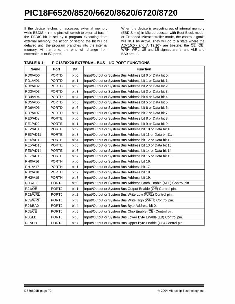
PIC18F6520/8520/6620/8620/6720/8720
If the device fetches or accesses external memorywhile EBDIS = 1, the pins will switch to external bus. Ifthe EBDIS bit is set by a program executing fromexternal memory, the action of setting the bit will bedelayed until the program branches into the internalmemory. At that time, the pins will change fromexternal bus to I/O ports.
When the device is executing out of internal memory(EBDIS = 0) in Microprocessor with Boot Block mode,or Extended Microcontroller mode, the control signalswill NOT be active. They will go to a state where theAD<15:0> and A<19:16> are tri-state; the CE, OE,WRH, WRL, UB and LB signals are ‘1’ and ALE andBA0 are ‘0’.
TABLE 6-1: PIC18F8X20 EXTERNAL BUS – I/O PORT FUNCTIONS
Name Port Bit Function
RD0/AD0 PORTD bit 0 Input/Output or System Bus Address bit 0 or Data bit 0.
RD1/AD1 PORTD bit 1 Input/Output or System Bus Address bit 1 or Data bit 1.
RD2/AD2 PORTD bit 2 Input/Output or System Bus Address bit 2 or Data bit 2.
RD3/AD3 PORTD bit 3 Input/Output or System Bus Address bit 3 or Data bit 3.
RD4/AD4 PORTD bit 4 Input/Output or System Bus Address bit 4 or Data bit 4.
RD5/AD5 PORTD bit 5 Input/Output or System Bus Address bit 5 or Data bit 5.
RD6/AD6 PORTD bit 6 Input/Output or System Bus Address bit 6 or Data bit 6.
RD7/AD7 PORTD bit 7 Input/Output or System Bus Address bit 7 or Data bit 7.
RE0/AD8 PORTE bit 0 Input/Output or System Bus Address bit 8 or Data bit 8.
RE1/AD9 PORTE bit 1 Input/Output or System Bus Address bit 9 or Data bit 9.
RE2/AD10 PORTE bit 2 Input/Output or System Bus Address bit 10 or Data bit 10.
RE3/AD11 PORTE bit 3 Input/Output or System Bus Address bit 11 or Data bit 11.
RE4/AD12 PORTE bit 4 Input/Output or System Bus Address bit 12 or Data bit 12.
RE5/AD13 PORTE bit 5 Input/Output or System Bus Address bit 13 or Data bit 13.
RE6/AD14 PORTE bit 6 Input/Output or System Bus Address bit 14 or Data bit 14.
RE7/AD15 PORTE bit 7 Input/Output or System Bus Address bit 15 or Data bit 15.
RH0/A16 PORTH bit 0 Input/Output or System Bus Address bit 16.
RH1/A17 PORTH bit 1 Input/Output or System Bus Address bit 17.
RH2/A18 PORTH bit 2 Input/Output or System Bus Address bit 18.
RH3/A19 PORTH bit 3 Input/Output or System Bus Address bit 19.
RJ0/ALE PORTJ bit 0 Input/Output or System Bus Address Latch Enable (ALE) Control pin.
RJ1/OE PORTJ bit 1 Input/Output or System Bus Output Enable (OE) Control pin.
RJ2/WRL PORTJ bit 2 Input/Output or System Bus Write Low (WRL) Control pin.
RJ3/WRH PORTJ bit 3 Input/Output or System Bus Write High (WRH) Control pin.
RJ4/BA0 PORTJ bit 4 Input/Output or System Bus Byte Address bit 0.
RJ5/CE PORTJ bit 5 Input/Output or System Bus Chip Enable (CE) Control pin.
RJ6/LB PORTJ bit 6 Input/Output or System Bus Lower Byte Enable (LB) Control pin.
RJ7/UB PORTJ bit 7 Input/Output or System Bus Upper Byte Enable (UB) Control pin.
DS39609B-page 72 2004 Microchip Technology Inc.

PIC18F6520/8520/6620/8620/6720/8720
6.2 16-bit Mode
The External Memory Interface implemented inPIC18F8X20 devices operates only in 16-bit mode.The mode selection is not software configurable, but isprogrammed via the configuration bits.
The WM<1:0> bits in the MEMCON register determinethree types of connections in 16-bit mode. They arereferred to as:
• 16-bit Byte Write• 16-bit Word Write• 16-bit Byte Select
These three different configurations allow the designermaximum flexibility in using 8-bit and 16-bit memorydevices.
For all 16-bit modes, the Address Latch Enable (ALE)pin indicates that the address bits A<15:0> areavailable on the External Memory Interface bus.Following the address latch, the Output Enable signal(OE) will enable both bytes of program memory at onceto form a 16-bit instruction word. The Chip Enablesignal (CE) is active at any time that the microcontrolleraccesses external memory, whether reading or writing;it is inactive (asserted high) whenever the device is inSleep mode.
In Byte Select mode, JEDEC standard Flash memorieswill require BA0 for the byte address line and one I/Oline to select between Byte and Word mode. The other16-bit modes do not need BA0. JEDEC standard staticRAM memories will use the UB or LB signals for byteselection.
6.2.1 16-BIT BYTE WRITE MODE
Figure 6-1 shows an example of 16-bit Byte Writemode for PIC18F8X20 devices. This mode is used fortwo separate 8-bit memories connected for 16-bit oper-ation. This generally includes basic EPROM and Flashdevices. It allows table writes to byte-wide externalmemories.
During a TBLWT instruction cycle, the TABLAT data ispresented on the upper and lower bytes of theAD15:AD0 bus. The appropriate WRH or WRL controlline is strobed on the LSb of the TBLPTR.
FIGURE 6-1: 16-BIT BYTE WRITE MODE EXAMPLE
AD<7:0>
A<19:16>
ALE
D<15:8>
373 A<x:0>
D<7:0>
A<19:0>A<x:0>
D<7:0>
373
OE
WRH
OE OEWR(1) WR(1)
CE CE
Note 1: This signal only applies to table writes. See Section 5.1 “Table Reads and Table Writes”.
WRL
D<7:0>
(LSB)(MSB)PIC18F8X20
D<7:0>
AD<15:8>
Address Bus
Data Bus
Control Lines
CE
2004 Microchip Technology Inc. DS39609B-page 73

PIC18F6520/8520/6620/8620/6720/8720
6.2.2 16-BIT WORD WRITE MODE
Figure 6-2 shows an example of 16-bit Word Writemode for PIC18F8X20 devices. This mode is used forword-wide memories, which includes some of theEPROM and Flash type memories. This mode allowsopcode fetches and table reads from all forms of 16-bitmemory and table writes to any type of word-wideexternal memories. This method makes a distinctionbetween TBLWT cycles to even or odd addresses.
During a TBLWT cycle to an even address(TBLPTR<0> = 0), the TABLAT data is transferred to aholding latch and the external address data bus istri-stated for the data portion of the bus cycle. No writesignals are activated.
During a TBLWT cycle to an odd address(TBLPTR<0> = 1), the TABLAT data is presented onthe upper byte of the AD15:AD0 bus. The contents ofthe holding latch are presented on the lower byte of theAD15:AD0 bus.
The WRH signal is strobed for each write cycle; theWRL pin is unused. The signal on the BA0 pin indicatesthe LSb of TBLPTR, but it is left unconnected. Instead,the UB and LB signals are active to select both bytes.The obvious limitation to this method is that the tablewrite must be done in pairs on a specific word boundaryto correctly write a word location.
FIGURE 6-2: 16-BIT WORD WRITE MODE EXAMPLE
AD<7:0>PIC18F8X20
AD<15:8>
ALE
373 A<20:1>
373
OE
WRH
A<19:16>
A<x:0>
D<15:0>
OE WR(1) CE
D<15:0>
JEDEC Word EPROM Memory
Address Bus
Data Bus
Control Lines
Note 1: This signal only applies to table writes. See Section 5.1 “Table Reads and Table Writes”.
CE
DS39609B-page 74 2004 Microchip Technology Inc.

PIC18F6520/8520/6620/8620/6720/8720
6.2.3 16-BIT BYTE SELECT MODE
Figure 6-3 shows an example of 16-bit Byte Selectmode for PIC18F8X20 devices. This mode allows tablewrite operations to word-wide external memories withbyte selection capability. This generally includes bothword-wide Flash and SRAM devices.
During a TBLWT cycle, the TABLAT data is presentedon the upper and lower byte of the AD15:AD0 bus. TheWRH signal is strobed for each write cycle; the WRLpin is not used. The BA0 or UB/LB signals are used toselect the byte to be written, based on the LeastSignificant bit of the TBLPTR register.
Flash and SRAM devices use different control signalcombinations to implement Byte Select mode. JEDECstandard Flash memories require that a controller I/Oport pin be connected to the memory’s BYTE/WORDpin to provide the select signal. They also use the BA0signal from the controller as a byte address. JEDECstandard static RAM memories, on the other hand, usethe UB or LB signals to select the byte.
FIGURE 6-3: 16-BIT BYTE SELECT MODE EXAMPLE
AD<7:0>PIC18F8X20
AD<15:8>
ALE
373 A<20:1>
373
OE
WRH
A<19:16>
WRL
BA0
JEDEC WordA<x:1>
D<15:0>
A<20:1>
CE
D<15:0>
I/O
OE WR(1)
A0
BYTE/WORD
Flash Memory
JEDEC WordA<x:1>
D<15:0>CE
D<15:0>
OE WR(1)
LB
UB
SRAM Memory
LB
UB
138
Address Bus
Data Bus
Control Lines
Note 1: This signal only applies to table writes. See Section 5.1 “Table Reads and Table Writes”.
2004 Microchip Technology Inc. DS39609B-page 75

PIC18F6520/8520/6620/8620/6720/8720
6.2.4 16-BIT MODE TIMING
The presentation of control signals on the externalmemory bus is different for the various operatingmodes. Typical signal timing diagrams are shown inFigure 6-4 through Figure 6-6.
FIGURE 6-4: EXTERNAL MEMORY BUS TIMING FOR TBLRD (MICROPROCESSOR MODE)
FIGURE 6-5: EXTERNAL MEMORY BUS TIMING FOR TBLRD (EXTENDED MICROCONTROLLER MODE)
Q2Q1 Q3 Q4 Q2Q1 Q3 Q4 Q4Q4 Q4 Q4
ALE
OE
3AABh
WRH
WRL
AD<15:0>
BA0
CF33h 9256h0E55h
‘1’ ‘1’
‘1’‘1’
Table Readof 92h
from 199E67h
1 TCY Wait
Q2Q1 Q3 Q4 Q2Q1 Q3 Q4 Q2Q1 Q3 Q4Apparent Q
Actual Q
A<19:16> 0Ch00h
CE ‘0’‘0’
MemoryCycle
InstructionExecution TBLRD Cycle 1 TBLRD Cycle 2
Opcode FetchMOVLW 55h
from 007556h
Q2Q1 Q3 Q4 Q2Q1 Q3 Q4 Q2Q1 Q3 Q4
A<19:16>
ALE
OE
AD<15:0>
CE
Opcode Fetch Opcode Fetch Opcode FetchTBLRD *
TBLRD Cycle 1
ADDLW 55hfrom 000100h
Q2Q1 Q3 Q4
0Ch
CF33h
TBLRD 92hfrom 199E67h
9256h
from 000104h
MemoryCycle
InstructionExecution INST(PC-2) TBLRD Cycle 2
MOVLW 55hfrom 000102h
MOVLW
DS39609B-page 76 2004 Microchip Technology Inc.

PIC18F6520/8520/6620/8620/6720/8720
FIGURE 6-6: EXTERNAL MEMORY BUS TIMING FOR SLEEP (MICROPROCESSOR MODE)
Q2Q1 Q3 Q4 Q2Q1 Q3 Q4
A<19:16>
ALE
OE
3AAAhAD<15:0>
00h 00h
CE
Opcode Fetch Opcode FetchSLEEP
SLEEP
from 007554h
Q1
Bus Inactive
0003h 3AABh 0E55h
MemoryCycle
InstructionExecution INST(PC-2)
Sleep Mode, MOVLW 55h
from 007556h
2004 Microchip Technology Inc. DS39609B-page 77
PIC18F6520/8520/6620/8620/6720/8720
NOTES:
DS39609B-page 78 2004 Microchip Technology Inc.

PIC18F6520/8520/6620/8620/6720/8720
7.0 DATA EEPROM MEMORY
The data EEPROM is readable and writable duringnormal operation over the entire VDD range. The datamemory is not directly mapped in the register filespace. Instead, it is indirectly addressed through theSpecial Function Registers (SFR).
There are five SFRs used to read and write theprogram and data EEPROM memory. These registersare:
• EECON1• EECON2• EEDATA
• EEADRH• EEADR
The EEPROM data memory allows byte read and write.When interfacing to the data memory block, EEDATAholds the 8-bit data for read/write. EEADR andEEADRH hold the address of the EEPROM locationbeing accessed. These devices have 1024 bytes ofdata EEPROM with an address range from 00h to3FFh.
The EEPROM data memory is rated for high erase/write cycles. A byte write automatically erases the loca-tion and writes the new data (erase-before-write). Thewrite time is controlled by an on-chip timer. The writetime will vary with voltage and temperature, as well asfrom chip to chip. Please refer to parameter D122 (seeSection 26.0 “Electrical Characteristics”) for exactlimits.
7.1 EEADR and EEADRH
The address register pair can address up to a maxi-mum of 1024 bytes of data EEPROM. The two MostSignificant bits of the address are stored in EEADRH,while the remaining eight Least Significant bits arestored in EEADR. The six Most Significant bits ofEEADRH are unused and are read as ‘0’.
7.2 EECON1 and EECON2 Registers
EECON1 is the control register for EEPROM memoryaccesses.
EECON2 is not a physical register. Reading EECON2will read all ‘0’s. The EECON2 register is usedexclusively in the EEPROM write sequence.
Control bits, RD and WR, initiate read and write opera-tions, respectively. These bits cannot be cleared, onlyset, in software. They are cleared in hardware at thecompletion of the read or write operation. The inabilityto clear the WR bit in software prevents the accidentalor premature termination of a write operation.
The WREN bit, when set, will allow a write operation.On power-up, the WREN bit is clear. The WRERR bit isset when a write operation is interrupted by a MCLRReset or a WDT Time-out Reset during normal opera-tion. In these situations, the user can check theWRERR bit and rewrite the location. It is necessary toreload the data and address registers (EEDATA andEEADR) due to the Reset condition forcing thecontents of the registers to zero.
Note: Interrupt flag bit, EEIF in the PIR2 register,is set when write is complete. It must becleared in software.
2004 Microchip Technology Inc. DS39609B-page 79

PIC18F6520/8520/6620/8620/6720/8720
REGISTER 7-1: EECON1 REGISTER (ADDRESS FA6h) R/W-x R/W-x U-0 R/W-0 R/W-x R/W-0 R/S-0 R/S-0
EEPGD CFGS — FREE WRERR WREN WR RD
bit 7 bit 0
bit 7 EEPGD: Flash Program/Data EEPROM Memory Select bit1 = Access Flash program memory0 = Access data EEPROM memory
bit 6 CFGS: Flash Program/Data EEPROM or Configuration Select bit
1 = Access configuration or calibration registers0 = Access Flash program or data EEPROM memory
bit 5 Unimplemented: Read as ‘0’
bit 4 FREE: Flash Row Erase Enable bit1 = Erase the program memory row addressed by TBLPTR on the next WR command
(cleared by completion of erase operation)0 = Perform write only
bit 3 WRERR: Flash Program/Data EEPROM Error Flag bit1 = A write operation is prematurely terminated
(any MCLR or any WDT Reset during self-timed programming in normal operation)0 = The write operation completed
Note: When a WRERR occurs, the EEPGD or FREE bits are not cleared. This allowstracing of the error condition.
bit 2 WREN: Flash Program/Data EEPROM Write Enable bit1 = Allows write cycles to Flash program/data EEPROM0 = Inhibits write cycles to Flash program/data EEPROM
bit 1 WR: Write Control bit1 = Initiates a data EEPROM erase/write cycle, or a program memory erase cycle or write cycle.
(The operation is self-timed and the bit is cleared by hardware once write is complete. TheWR bit can only be set (not cleared) in software.)
0 = Write cycle to the EEPROM is complete
bit 0 RD: Read Control bit1 = Initiates an EEPROM read. (Read takes one cycle. RD is cleared in hardware. The RD bit
can only be set (not cleared) in software. RD bit cannot be set when EEPGD = 1.)0 = Does not initiate an EEPROM read
Legend:
R = Readable bit W = Writable bit U = Unimplemented bit, read as ‘0’
- n = Value at POR ‘1’ = Bit is set ‘0’ = Bit is cleared x = Bit is unknown
DS39609B-page 80 2004 Microchip Technology Inc.

PIC18F6520/8520/6620/8620/6720/8720
7.3 Reading the Data EEPROM Memory
To read a data memory location, the user must write theaddress to the EEADRH:EEADR register pair, clear theEEPGD control bit (EECON1<7>), clear the CFGS
control bit (EECON1<6>) and then set the RD controlbit (EECON1<0>). The data is available for the verynext instruction cycle; therefore, the EEDATA registercan be read by the next instruction. EEDATA will holdthis value until another read operation, or until it iswritten to by the user (during a write operation).
EXAMPLE 7-1: DATA EEPROM READ
7.4 Writing to the Data EEPROM Memory
To write an EEPROM data location, the address mustfirst be written to the EEADRH:EEADR register pairand the data written to the EEDATA register. Then thesequence in Example 7-2 must be followed to initiatethe write cycle.
The write will not initiate if the above sequence is notexactly followed (write 55h to EECON2, write AAh toEECON2, then set WR bit) for each byte. It is stronglyrecommended that interrupts be disabled during thiscode segment.
Additionally, the WREN bit in EECON1 must be set toenable writes. This mechanism prevents accidentalwrites to data EEPROM due to unexpected codeexecution (i.e., runaway programs). The WREN bit
should be kept clear at all times, except when updatingthe EEPROM. The WREN bit is not clearedby hardware
After a write sequence has been initiated, EECON1,EEADRH, EEADR and EEDATA cannot be modified.The WR bit will be inhibited from being set unless theWREN bit is set. Both WR and WREN cannot be setwith the same instruction.
At the completion of the write cycle, the WR bit iscleared in hardware and the EEPROM Write CompleteInterrupt Flag bit (EEIF) is set. The user may eitherenable this interrupt, or poll this bit. EEIF must becleared by software.
EXAMPLE 7-2: DATA EEPROM WRITE
MOVLW DATA_EE_ADDRH ;MOVWF EEADRH ; Upper bits of Data Memory Address to readMOVLW DATA_EE_ADDR ;MOVWF EEADR ; Lower bits of Data Memory Address to readBCF EECON1, EEPGD ; Point to DATA memoryBCF EECON1, CFGS ; Access EEPROMBSF EECON1, RD ; EEPROM ReadMOVF EEDATA, W ; W = EEDATA
MOVLW DATA_EE_ADDRH ;MOVWF EEADRH ; Upper bits of Data Memory Address to writeMOVLW DATA_EE_ADDR ;MOVWF EEADR ; Lower bits of Data Memory Address to writeMOVLW DATA_EE_DATA ;MOVWF EEDATA ; Data Memory Value to writeBCF EECON1, EEPGD ; Point to DATA memoryBCF EECON1, CFGS ; Access EEPROMBSF EECON1, WREN ; Enable writes
BCF INTCON, GIE ; Disable InterruptsMOVLW 55h ;
Required MOVWF EECON2 ; Write 55hSequence MOVLW AAh ;
MOVWF EECON2 ; Write AAhBSF EECON1, WR ; Set WR bit to begin writeBSF INTCON, GIE ; Enable Interrupts
; User code executionBCF EECON1, WREN ; Disable writes on write complete (EEIF set)
2004 Microchip Technology Inc. DS39609B-page 81

PIC18F6520/8520/6620/8620/6720/8720
7.5 Write Verify
Depending on the application, good programmingpractice may dictate that the value written to the mem-ory should be verified against the original value. Thisshould be used in applications where excessive writescan stress bits near the specification limit.
7.6 Protection Against Spurious Write
There are conditions when the user may not want towrite to the data EEPROM memory. To protect againstspurious EEPROM writes, various mechanisms havebeen built-in. On power-up, the WREN bit is cleared.Also, the Power-up Timer (72 ms duration) preventsEEPROM write.
The write initiate sequence and the WREN bit togetherhelp prevent an accidental write during brown-out,power glitch, or software malfunction.
7.7 Operation During Code-Protect
Data EEPROM memory has its own code-protectmechanism. External read and write operations aredisabled if either of these mechanisms are enabled.
The microcontroller itself can both read and write to theinternal data EEPROM, regardless of the state of thecode-protect configuration bit. Refer to Section 23.0“Special Features of the CPU” for additionalinformation.
7.8 Using the Data EEPROM
The data EEPROM is a high endurance, byte address-able array that has been optimized for the storage offrequently changing information (e.g., program vari-ables or other data that are updated often). Frequentlychanging values will typically be updated more oftenthan specification D124. If this is not the case, an arrayrefresh must be performed. For this reason, variablesthat change infrequently (such as constants, IDs,calibration, etc.) should be stored in Flash programmemory.
A simple data EEPROM refresh routine is shown inExample 7-3.
EXAMPLE 7-3: DATA EEPROM REFRESH ROUTINE
Note: If data EEPROM is only used to storeconstants and/or data that changes rarely,an array refresh is likely not required. Seespecification D124.
CLRF EEADR ; Start at address 0CLRF EEADRH ;BCF EECON1, CFGS ; Set for memoryBCF EECON1, EEPGD ; Set for Data EEPROMBCF INTCON, GIE ; Disable interruptsBSF EECON1, WREN ; Enable writes
Loop ; Loop to refresh arrayBSF EECON1, RD ; Read current addressMOVLW 55h ;MOVWF EECON2 ; Write 55hMOVLW AAh ;MOVWF EECON2 ; Write AAhBSF EECON1, WR ; Set WR bit to begin writeBTFSC EECON1, WR ; Wait for write to completeBRA $-2INCFSZ EEADR, F ; Increment addressBRA Loop ; Not zero, do it againINCFSZ EEADRH, F ; Increment the high addressBRA Loop ; Not zero, do it again
BCF EECON1, WREN ; Disable writesBSF INTCON, GIE ; Enable interrupts
DS39609B-page 82 2004 Microchip Technology Inc.

PIC18F6520/8520/6620/8620/6720/8720
TABLE 7-1: REGISTERS ASSOCIATED WITH DATA EEPROM MEMORY
Name Bit 7 Bit 6 Bit 5 Bit 4 Bit 3 Bit 2 Bit 1 Bit 0Value on
POR, BOR
Value on all other Resets
INTCON GIE/GIEH PEIE/GIEL TMR0IE INT0IE RBIE TMR0IF INT0IF RBIF 0000 0000 0000 0000
EEADRH — — — — — — EE Addr Register High ---- --00 ---- --00
EEADR EEPROM Address Register 0000 0000 0000 0000
EEDATA EEPROM Data Register 0000 0000 0000 0000
EECON2 EEPROM Control Register 2 (not a physical register) ---- ---- ---- ----
EECON1 EEPGD CFGS — FREE WRERR WREN WR RD xx-0 x000 uu-0 u000
IPR2 — CMIP — EEIP BCLIP LVDIP TMR3IP CCP2IP ---1 1111 ---1 1111
PIR2 — CMIF — EEIF BCLIF LVDIF TMR3IF CCP2IF ---0 0000 ---0 0000
PIE2 — CMIE — EEIE BCLIE LVDIE TMR3IE CCP2IE ---0 0000 ---0 0000
Legend: x = unknown, u = unchanged, r = reserved, – = unimplemented, read as ‘0’. Shaded cells are not used during Flash/EEPROM access.
2004 Microchip Technology Inc. DS39609B-page 83

PIC18F6520/8520/6620/8620/6720/8720
NOTES:
DS39609B-page 84 2004 Microchip Technology Inc.

PIC18F6520/8520/6620/8620/6720/8720
8.0 8 X 8 HARDWARE MULTIPLIER
8.1 Introduction
An 8 x 8 hardware multiplier is included in the ALU ofthe PIC18FXX20 devices. By making the multiply ahardware operation, it completes in a single instructioncycle. This is an unsigned multiply that gives a 16-bitresult. The result is stored in the 16-bit product registerpair (PRODH:PRODL). The multiplier does not affectany flags in the ALUSTA register.
Making the 8 x 8 multiplier execute in a single cyclegives the following advantages:
• Higher computational throughput• Reduces code size requirements for multiply
algorithms
The performance increase allows the device to be usedin applications previously reserved for Digital SignalProcessors.
Table 8-1 shows a performance comparison betweenenhanced devices using the single-cycle hardwaremultiply and performing the same function without thehardware multiply.
8.2 Operation
Example 8-1 shows the sequence to do an 8 x 8unsigned multiply. Only one instruction is requiredwhen one argument of the multiply is already loaded inthe WREG register.
Example 8-2 shows the sequence to do an 8 x 8 signedmultiply. To account for the sign bits of the arguments,each argument’s Most Significant bit (MSb) is testedand the appropriate subtractions are done.
EXAMPLE 8-1: 8 x 8 UNSIGNED MULTIPLY ROUTINE
EXAMPLE 8-2: 8 x 8 SIGNED MULTIPLY ROUTINE
TABLE 8-1: PERFORMANCE COMPARISON
MOVF ARG1, W ; MULWF ARG2 ; ARG1 * ARG2 ->
; PRODH:PRODL
MOVF ARG1, W ;MULWF ARG2 ; ARG1 * ARG2 ->
; PRODH:PRODL BTFSC ARG2, SB ; Test Sign Bit SUBWF PRODH, F ; PRODH = PRODH
; - ARG1 MOVF ARG2, W ;BTFSC ARG1, SB ; Test Sign Bit SUBWF PRODH, F ; PRODH = PRODH
; - ARG2
Routine Multiply MethodProgramMemory(Words)
Cycles(Max)
Time
@ 40 MHz @ 10 MHz @ 4 MHz
8 x 8 unsignedWithout hardware multiply 13 69 6.9 µs 27.6 µs 69 µs
Hardware multiply 1 1 100 ns 400 ns 1 µs
8 x 8 signedWithout hardware multiply 33 91 9.1 µs 36.4 µs 91 µs
Hardware multiply 6 6 600 ns 2.4 µs 6 µs
16 x 16 unsignedWithout hardware multiply 21 242 24.2 µs 96.8 µs 242 µs
Hardware multiply 28 28 2.8 µs 11.2 µs 28 µs
16 x 16 signedWithout hardware multiply 52 254 25.4 µs 102.6 µs 254 µs
Hardware multiply 35 40 4.0 µs 16.0 µs 40 µs
2004 Microchip Technology Inc. DS39609B-page 85

PIC18F6520/8520/6620/8620/6720/8720
Example 8-3 shows the sequence to do a 16 x 16unsigned multiply. Equation 8-1 shows the algorithmthat is used. The 32-bit result is stored in four registers,RES3:RES0.
EQUATION 8-1: 16 x 16 UNSIGNED MULTIPLICATION ALGORITHM
EXAMPLE 8-3: 16 x 16 UNSIGNED MULTIPLY ROUTINE
Example 8-4 shows the sequence to do a 16 x 16signed multiply. Equation 8-2 shows the algorithmused. The 32-bit result is stored in four registers,RES3:RES0. To account for the sign bits of the argu-ments, each argument pairs’ Most Significant bit (MSb)is tested and the appropriate subtractions are done.
EQUATION 8-2: 16 x 16 SIGNED MULTIPLICATION ALGORITHM
EXAMPLE 8-4: 16 x 16 SIGNED MULTIPLY ROUTINE
MOVF ARG1L, W MULWF ARG2L ; ARG1L * ARG2L ->
; PRODH:PRODL MOVFF PRODH, RES1 ; MOVFF PRODL, RES0 ;
; MOVF ARG1H, W MULWF ARG2H ; ARG1H * ARG2H ->
; PRODH:PRODL MOVFF PRODH, RES3 ; MOVFF PRODL, RES2 ;
; MOVF ARG1L, W MULWF ARG2H ; ARG1L * ARG2H ->
; PRODH:PRODL MOVF PRODL, W ; ADDWF RES1, F ; Add cross MOVF PRODH, W ; products ADDWFC RES2, F ; CLRF WREG ; ADDWFC RES3, F ;
; MOVF ARG1H, W ; MULWF ARG2L ; ARG1H * ARG2L ->
; PRODH:PRODL MOVF PRODL, W ; ADDWF RES1, F ; Add cross MOVF PRODH, W ; products ADDWFC RES2, F ; CLRF WREG ; ADDWFC RES3, F ;
RES3:RES0 = ARG1H:ARG1L • ARG2H:ARG2L= (ARG1H • ARG2H • 216) +
(ARG1H • ARG2L • 28) +(ARG1L • ARG2H • 28) +(ARG1L • ARG2L)
MOVF ARG1L, W MULWF ARG2L ; ARG1L * ARG2L ->
; PRODH:PRODL MOVFF PRODH, RES1 ; MOVFF PRODL, RES0 ;
; MOVF ARG1H, W MULWF ARG2H ; ARG1H * ARG2H ->
; PRODH:PRODL MOVFF PRODH, RES3 ; MOVFF PRODL, RES2 ;
; MOVF ARG1L, W MULWF ARG2H ; ARG1L * ARG2H ->
; PRODH:PRODL MOVF PRODL, W ; ADDWF RES1, F ; Add cross MOVF PRODH, W ; products ADDWFC RES2, F ; CLRF WREG ; ADDWFC RES3, F ;
; MOVF ARG1H, W ; MULWF ARG2L ; ARG1H * ARG2L ->
; PRODH:PRODL MOVF PRODL, W ; ADDWF RES1, F ; Add cross MOVF PRODH, W ; products ADDWFC RES2, F ; CLRF WREG ; ADDWFC RES3, F ;
; BTFSS ARG2H, 7 ; ARG2H:ARG2L neg? BRA SIGN_ARG1 ; no, check ARG1 MOVF ARG1L, W ; SUBWF RES2 ; MOVF ARG1H, W ; SUBWFB RES3
; SIGN_ARG1
BTFSS ARG1H, 7 ; ARG1H:ARG1L neg? BRA CONT_CODE ; no, done MOVF ARG2L, W ; SUBWF RES2 ; MOVF ARG2H, W ; SUBWFB RES3
; CONT_CODE :
RES3:RES0= ARG1H:ARG1L • ARG2H:ARG2L= (ARG1H • ARG2H • 216) +
(ARG1H • ARG2L • 28) +(ARG1L • ARG2H • 28) +(ARG1L • ARG2L) +(-1 • ARG2H<7> • ARG1H:ARG1L • 216) +(-1 • ARG1H<7> • ARG2H:ARG2L • 216)
DS39609B-page 86 2004 Microchip Technology Inc.

PIC18F6520/8520/6620/8620/6720/8720
9.0 INTERRUPTS
The PIC18FXX20 devices have multiple interruptsources and an interrupt priority feature that allowseach interrupt source to be assigned a high or a lowpriority level. The high priority interrupt vector is at000008h, while the low priority interrupt vector is at000018h. High priority interrupt events will override anylow priority interrupts that may be in progress.
There are thirteen registers which are used to controlinterrupt operation. They are:
• RCON
• INTCON• INTCON2• INTCON3
• PIR1, PIR2, PIR3• PIE1, PIE2, PIE3• IPR1, IPR2, IPR3
It is recommended that the Microchip header files,supplied with MPLAB® IDE, be used for the symbolic bitnames in these registers. This allows the assembler/compiler to automatically take care of the placement ofthese bits within the specified register.
Each interrupt source has three bits to control itsoperation. The functions of these bits are:
• Flag bit to indicate that an interrupt event occurred
• Enable bit that allows program execution to branch to the interrupt vector address when the flag bit is set
• Priority bit to select high priority or low priority
The interrupt priority feature is enabled by setting theIPEN bit (RCON<7>). When interrupt priority isenabled, there are two bits which enable interruptsglobally. Setting the GIEH bit (INTCON<7>) enables allinterrupts that have the priority bit set. Setting the GIELbit (INTCON<6>) enables all interrupts that have thepriority bit cleared. When the interrupt flag, enable bitand appropriate global interrupt enable bit are set, theinterrupt will vector immediately to address 000008h or000018h, depending on the priority level. Individualinterrupts can be disabled through their correspondingenable bits.
When the IPEN bit is cleared (default state), theinterrupt priority feature is disabled and interrupts arecompatible with PICmicro® mid-range devices. In Com-patibility mode, the interrupt priority bits for each sourcehave no effect. INTCON<6> is the PEIE bit, whichenables/disables all peripheral interrupt sources.INTCON<7> is the GIE bit, which enables/disables allinterrupt sources. All interrupts branch to address000008h in Compatibility mode.
When an interrupt is responded to, the Global InterruptEnable bit is cleared to disable further interrupts. If theIPEN bit is cleared, this is the GIE bit. If interrupt prioritylevels are used, this will be either the GIEH or GIEL bit.High priority interrupt sources can interrupt a lowpriority interrupt.
The return address is pushed onto the stack and thePC is loaded with the interrupt vector address(000008h or 000018h). Once in the Interrupt ServiceRoutine, the source(s) of the interrupt can be deter-mined by polling the interrupt flag bits. The interruptflag bits must be cleared in software before re-enablinginterrupts to avoid recursive interrupts.
The “return from interrupt” instruction, RETFIE, exitsthe interrupt routine and sets the GIE bit (GIEH or GIELif priority levels are used), which re-enables interrupts.
For external interrupt events, such as the INT pins orthe PORTB input change interrupt, the interrupt latencywill be three to four instruction cycles. The exactlatency is the same for one or two-cycle instructions.Individual interrupt flag bits are set, regardless of thestatus of their corresponding enable bit or the GIE bit.
2004 Microchip Technology Inc. DS39609B-page 87

PIC18F6520/8520/6620/8620/6720/8720
FIGURE 9-1: INTERRUPT LOGIC
TMR0IE
GIEH/GIE
GIEL/PEIE
Wake-up if in Sleep mode
Interrupt to CPUVector to Location0008h
INT2IFINT2IEINT2IP
INT1IFINT1IEINT1IP
TMR0IFTMR0IETMR0IP
RBIFRBIERBIP
IPEN
TMR0IF
TMR0IP
INT1IFINT1IEINT1IPINT2IFINT2IEINT2IP
RBIFRBIERBIP
INT0IFINT0IE
GIEL/PEIE
Interrupt to CPUVector to Location
IPEN
IPEN
0018h
Peripheral Interrupt Flag bitPeripheral Interrupt Enable bitPeripheral Interrupt Priority bit
Peripheral Interrupt Flag bitPeripheral Interrupt Enable bitPeripheral Interrupt Priority bit
TMR1IFTMR1IETMR1IP
XXXXIFXXXXIEXXXXIP
Additional Peripheral Interrupts
TMR1IFTMR1IETMR1IP
High Priority Interrupt Generation
Low Priority Interrupt Generation
XXXXIFXXXXIEXXXXIP
Additional Peripheral Interrupts
GIE/GEIH
DS39609B-page 88 2004 Microchip Technology Inc.

PIC18F6520/8520/6620/8620/6720/8720
9.1 INTCON Registers
The INTCON registers are readable and writableregisters, which contain various enable, priority andflag bits.
REGISTER 9-1: INTCON REGISTER
Note: Interrupt flag bits are set when an interruptcondition occurs, regardless of the state ofits corresponding enable bit or the globalenable bit. User software should ensurethe appropriate interrupt flag bits are clearprior to enabling an interrupt. This featureallows for software polling.
R/W-0 R/W-0 R/W-0 R/W-0 R/W-0 R/W-0 R/W-0 R/W-x
GIE/GIEH PEIE/GIEL TMR0IE INT0IE RBIE TMR0IF INT0IF RBIF
bit 7 bit 0
bit 7 GIE/GIEH: Global Interrupt Enable bit
When IPEN (RCON<7>) = 0:1 = Enables all unmasked interrupts0 = Disables all interrupts When IPEN (RCON<7>) = 1:1 = Enables all high priority interrupts 0 = Disables all interrupts
bit 6 PEIE/GIEL: Peripheral Interrupt Enable bit
When IPEN (RCON<7>) = 0:1 = Enables all unmasked peripheral interrupts 0 = Disables all peripheral interrupts When IPEN (RCON<7>) = 1:1 = Enables all low priority peripheral interrupts 0 = Disables all low priority peripheral interrupts
bit 5 TMR0IE: TMR0 Overflow Interrupt Enable bit
1 = Enables the TMR0 overflow interrupt 0 = Disables the TMR0 overflow interrupt
bit 4 INT0IE: INT0 External Interrupt Enable bit 1 = Enables the INT0 external interrupt 0 = Disables the INT0 external interrupt
bit 3 RBIE: RB Port Change Interrupt Enable bit 1 = Enables the RB port change interrupt 0 = Disables the RB port change interrupt
bit 2 TMR0IF: TMR0 Overflow Interrupt Flag bit
1 = TMR0 register has overflowed (must be cleared in software) 0 = TMR0 register did not overflow
bit 1 INT0IF: INT0 External Interrupt Flag bit 1 = The INT0 external interrupt occurred (must be cleared in software) 0 = The INT0 external interrupt did not occur
bit 0 RBIF: RB Port Change Interrupt Flag bit 1 = At least one of the RB7:RB4 pins changed state (must be cleared in software) 0 = None of the RB7:RB4 pins have changed state
Note: A mismatch condition will continue to set this bit. Reading PORTB will end the mismatch condition and allow the bit to be cleared.
Legend:
R = Readable bit W = Writable bit U = Unimplemented bit, read as ‘0’
- n = Value at POR ‘1’ = Bit is set ‘0’ = Bit is cleared x = Bit is unknown
2004 Microchip Technology Inc. DS39609B-page 89

PIC18F6520/8520/6620/8620/6720/8720
REGISTER 9-2: INTCON2 REGISTER
R/W-1 R/W-1 R/W-1 R/W-1 R/W-1 R/W-1 R/W-1 R/W-1
RBPU INTEDG0 INTEDG1 INTEDG2 INTEDG3 TMR0IP INT3IP RBIP
bit 7 bit 0
bit 7 RBPU: PORTB Pull-up Enable bit 1 = All PORTB pull-ups are disabled 0 = PORTB pull-ups are enabled by individual port latch values
bit 6 INTEDG0: External Interrupt 0 Edge Select bit 1 = Interrupt on rising edge 0 = Interrupt on falling edge
bit 5 INTEDG1: External Interrupt 1 Edge Select bit
1 = Interrupt on rising edge 0 = Interrupt on falling edge
bit 4 INTEDG2: External Interrupt 2 Edge Select bit 1 = Interrupt on rising edge 0 = Interrupt on falling edge
bit 3 INTEDG3: External Interrupt 3 Edge Select bit 1 = Interrupt on rising edge 0 = Interrupt on falling edge
bit 2 TMR0IP: TMR0 Overflow Interrupt Priority bit
1 = High priority 0 = Low priority
bit 1 INT3IP: INT3 External Interrupt Priority bit1 = High priority 0 = Low priority
bit 0 RBIP: RB Port Change Interrupt Priority bit1 = High priority 0 = Low priority
Legend:
R = Readable bit W = Writable bit U = Unimplemented bit, read as ‘0’
- n = Value at POR ‘1’ = Bit is set ‘0’ = Bit is cleared x = Bit is unknown
Note: Interrupt flag bits are set when an interrupt condition occurs, regardless of the stateof its corresponding enable bit or the global enable bit. User software should ensurethe appropriate interrupt flag bits are clear prior to enabling an interrupt. This featureallows for software polling.
DS39609B-page 90 2004 Microchip Technology Inc.

PIC18F6520/8520/6620/8620/6720/8720
REGISTER 9-3: INTCON3 REGISTER
R/W-1 R/W-1 R/W-0 R/W-0 R/W-0 R/W-0 R/W-0 R/W-0
INT2IP INT1IP INT3IE INT2IE INT1IE INT3IF INT2IF INT1IF
bit 7 bit 0
bit 7 INT2IP: INT2 External Interrupt Priority bit1 = High priority 0 = Low priority
bit 6 INT1IP: INT1 External Interrupt Priority bit
1 = High priority 0 = Low priority
bit 5 INT3IE: INT3 External Interrupt Enable bit1 = Enables the INT3 external interrupt 0 = Disables the INT3 external interrupt
bit 4 INT2IE: INT2 External Interrupt Enable bit1 = Enables the INT2 external interrupt 0 = Disables the INT2 external interrupt
bit 3 INT1IE: INT1 External Interrupt Enable bit
1 = Enables the INT1 external interrupt 0 = Disables the INT1 external interrupt
bit 2 INT3IF: INT3 External Interrupt Flag bit1 = The INT3 external interrupt occurred (must be cleared in software) 0 = The INT3 external interrupt did not occur
bit 1 INT2IF: INT2 External Interrupt Flag bit1 = The INT2 external interrupt occurred (must be cleared in software) 0 = The INT2 external interrupt did not occur
bit 0 INT1IF: INT1 External Interrupt Flag bit
1 = The INT1 external interrupt occurred (must be cleared in software) 0 = The INT1 external interrupt did not occur
Legend:
R = Readable bit W = Writable bit U = Unimplemented bit, read as ‘0’
- n = Value at POR ‘1’ = Bit is set ‘0’ = Bit is cleared x = Bit is unknown
Note: Interrupt flag bits are set when an interrupt condition occurs, regardless of the stateof its corresponding enable bit or the global enable bit. User software should ensurethe appropriate interrupt flag bits are clear prior to enabling an interrupt. This featureallows for software polling.
2004 Microchip Technology Inc. DS39609B-page 91

PIC18F6520/8520/6620/8620/6720/8720
9.2 PIR Registers
The PIR registers contain the individual flag bits for theperipheral interrupts. Due to the number of peripheralinterrupt sources, there are three Peripheral InterruptFlag Registers (PIR1, PIR2 and PIR3).
REGISTER 9-4: PIR1: PERIPHERAL INTERRUPT REQUEST (FLAG) REGISTER 1
Note 1: Interrupt flag bits are set when an interruptcondition occurs, regardless of the state ofits corresponding enable bit or the globalenable bit, GIE (INTCON<7>).
2: User software should ensure the appropri-ate interrupt flag bits are cleared prior toenabling an interrupt and after servicingthat interrupt.
R/W-0 R/W-0 R-0 R-0 R/W-0 R/W-0 R/W-0 R/W-0
PSPIF(1) ADIF RC1IF TX1IF SSPIF CCP1IF TMR2IF TMR1IF
bit 7 bit 0
bit 7 PSPIF: Parallel Slave Port Read/Write Interrupt Flag bit(1)
1 = A read or a write operation has taken place (must be cleared in software) 0 = No read or write has occurred
bit 6 ADIF: A/D Converter Interrupt Flag bit 1 = An A/D conversion completed (must be cleared in software) 0 = The A/D conversion is not complete
bit 5 RC1IF: USART1 Receive Interrupt Flag bit
1 = The USART1 receive buffer, RCREG, is full (cleared when RCREG is read) 0 = The USART1 receive buffer is empty
bit 4 TX1IF: USART Transmit Interrupt Flag bit 1 = The USART1 transmit buffer, TXREG, is empty (cleared when TXREG is written) 0 = The USART1 transmit buffer is full
bit 3 SSPIF: Master Synchronous Serial Port Interrupt Flag bit 1 = The transmission/reception is complete (must be cleared in software)0 = Waiting to transmit/receive
bit 2 CCP1IF: CCP1 Interrupt Flag bit
Capture mode: 1 = A TMR1 register capture occurred (must be cleared in software) 0 = No TMR1 register capture occurred Compare mode: 1 = A TMR1 register compare match occurred (must be cleared in software) 0 = No TMR1 register compare match occurredPWM mode: Unused in this mode.
bit 1 TMR2IF: TMR2 to PR2 Match Interrupt Flag bit
1 = TMR2 to PR2 match occurred (must be cleared in software) 0 = No TMR2 to PR2 match occurred
bit 0 TMR1IF: TMR1 Overflow Interrupt Flag bit 1 = TMR1 register overflowed (must be cleared in software)0 = TMR1 register did not overflow
Note 1: Enabled only in Microcontroller mode for PIC18F8X20 devices.
Legend:
R = Readable bit W = Writable bit U = Unimplemented bit, read as ‘0’
- n = Value at POR ‘1’ = Bit is set ‘0’ = Bit is cleared x = Bit is unknown
DS39609B-page 92 2004 Microchip Technology Inc.
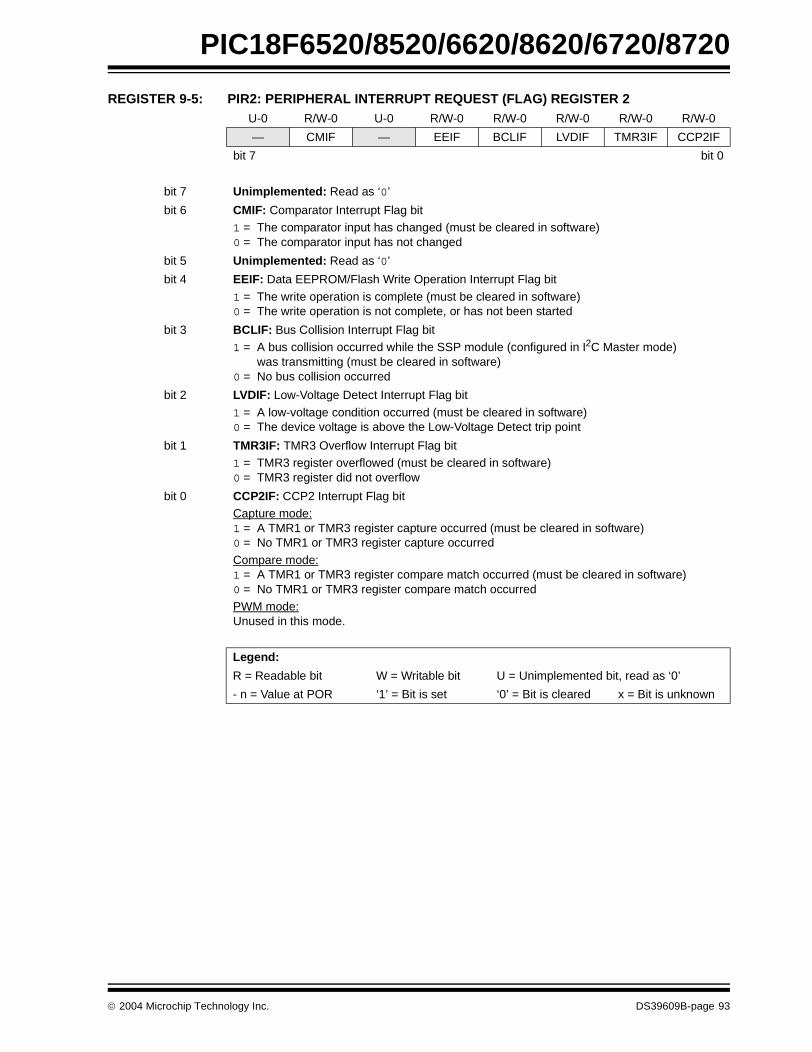
PIC18F6520/8520/6620/8620/6720/8720
REGISTER 9-5: PIR2: PERIPHERAL INTERRUPT REQUEST (FLAG) REGISTER 2 U-0 R/W-0 U-0 R/W-0 R/W-0 R/W-0 R/W-0 R/W-0
— CMIF — EEIF BCLIF LVDIF TMR3IF CCP2IF
bit 7 bit 0
bit 7 Unimplemented: Read as ‘0’
bit 6 CMIF: Comparator Interrupt Flag bit1 = The comparator input has changed (must be cleared in software)0 = The comparator input has not changed
bit 5 Unimplemented: Read as ‘0’
bit 4 EEIF: Data EEPROM/Flash Write Operation Interrupt Flag bit
1 = The write operation is complete (must be cleared in software)0 = The write operation is not complete, or has not been started
bit 3 BCLIF: Bus Collision Interrupt Flag bit 1 = A bus collision occurred while the SSP module (configured in I2C Master mode)
was transmitting (must be cleared in software)0 = No bus collision occurred
bit 2 LVDIF: Low-Voltage Detect Interrupt Flag bit
1 = A low-voltage condition occurred (must be cleared in software)0 = The device voltage is above the Low-Voltage Detect trip point
bit 1 TMR3IF: TMR3 Overflow Interrupt Flag bit1 = TMR3 register overflowed (must be cleared in software)0 = TMR3 register did not overflow
bit 0 CCP2IF: CCP2 Interrupt Flag bit Capture mode: 1 = A TMR1 or TMR3 register capture occurred (must be cleared in software) 0 = No TMR1 or TMR3 register capture occurred
Compare mode: 1 = A TMR1 or TMR3 register compare match occurred (must be cleared in software) 0 = No TMR1 or TMR3 register compare match occurredPWM mode:Unused in this mode.
Legend:
R = Readable bit W = Writable bit U = Unimplemented bit, read as ‘0’
- n = Value at POR ‘1’ = Bit is set ‘0’ = Bit is cleared x = Bit is unknown
2004 Microchip Technology Inc. DS39609B-page 93

PIC18F6520/8520/6620/8620/6720/8720
REGISTER 9-6: PIR3: PERIPHERAL INTERRUPT REQUEST (FLAG) REGISTER 3 U-0 U-0 R-0 R-0 R/W-0 R/W-0 R/W-0 R/W-0
— — RC2IF TX2IF TMR4IF CCP5IF CCP4IF CCP3IF
bit 7 bit 0
bit 7- 6 Unimplemented: Read as ‘0’
bit 5 RC2IF: USART2 Receive Interrupt Flag bit 1 = The USART2 receive buffer, RCREG, is full (cleared when RCREG is read) 0 = The USART2 receive buffer is empty
bit 4 TX2IF: USART2 Transmit Interrupt Flag bit 1 = The USART2 transmit buffer, TXREG, is empty (cleared when TXREG is written) 0 = The USART2 transmit buffer is full
bit 3 TMR4IF: TMR3 Overflow Interrupt Flag bit
1 = TMR4 register overflowed (must be cleared in software)0 = TMR4 register did not overflow
bit 2-0 CCPxIF: CCPx Interrupt Flag bit (CCP Modules 3, 4 and 5)Capture mode: 1 = A TMR1 or TMR3 register capture occurred (must be cleared in software) 0 = No TMR1 or TMR3 register capture occurred Compare mode: 1 = A TMR1 or TMR3 register compare match occurred (must be cleared in software) 0 = No TMR1 or TMR3 register compare match occurred
PWM mode:Unused in this mode.
Legend:
R = Readable bit W = Writable bit U = Unimplemented bit, read as ‘0’
- n = Value at POR ‘1’ = Bit is set ‘0’ = Bit is cleared x = Bit is unknown
DS39609B-page 94 2004 Microchip Technology Inc.

PIC18F6520/8520/6620/8620/6720/8720
9.3 PIE Registers
The PIE registers contain the individual enable bits forthe peripheral interrupts. Due to the number ofperipheral interrupt sources, there are three PeripheralInterrupt Enable registers (PIE1, PIE2 and PIE3).When the IPEN bit (RCON<7>) is ‘0’, the PEIE bit mustbe set to enable any of these peripheral interrupts.
REGISTER 9-7: PIE1: PERIPHERAL INTERRUPT ENABLE REGISTER 1 R/W-0 R/W-0 R/W-0 R/W-0 R/W-0 R/W-0 R/W-0 R/W-0
PSPIE(1) ADIE RC1IE TX1IE SSPIE CCP1IE TMR2IE TMR1IE
bit 7 bit 0
bit 7 PSPIE: Parallel Slave Port Read/Write Interrupt Enable bit(1)
1 = Enables the PSP read/write interrupt 0 = Disables the PSP read/write interrupt
bit 6 ADIE: A/D Converter Interrupt Enable bit 1 = Enables the A/D interrupt 0 = Disables the A/D interrupt
bit 5 RC1IE: USART1 Receive Interrupt Enable bit
1 = Enables the USART1 receive interrupt 0 = Disables the USART1 receive interrupt
bit 4 TX1IE: USART1 Transmit Interrupt Enable bit 1 = Enables the USART1 transmit interrupt 0 = Disables the USART1 transmit interrupt
bit 3 SSPIE: Master Synchronous Serial Port Interrupt Enable bit1 = Enables the MSSP interrupt 0 = Disables the MSSP interrupt
bit 2 CCP1IE: CCP1 Interrupt Enable bit
1 = Enables the CCP1 interrupt 0 = Disables the CCP1 interrupt
bit 1 TMR2IE: TMR2 to PR2 Match Interrupt Enable bit1 = Enables the TMR2 to PR2 match interrupt 0 = Disables the TMR2 to PR2 match interrupt
bit 0 TMR1IE: TMR1 Overflow Interrupt Enable bit1 = Enables the TMR1 overflow interrupt 0 = Disables the TMR1 overflow interrupt
Note 1: Enabled only in Microcontroller mode for PIC18F8X20 devices.
Legend:
R = Readable bit W = Writable bit U = Unimplemented bit, read as ‘0’
- n = Value at POR ‘1’ = Bit is set ‘0’ = Bit is cleared x = Bit is unknown
2004 Microchip Technology Inc. DS39609B-page 95
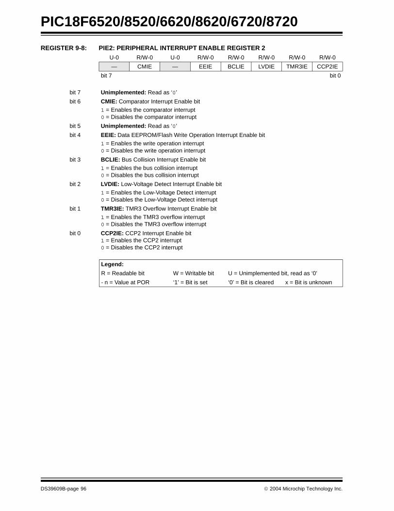
PIC18F6520/8520/6620/8620/6720/8720
REGISTER 9-8: PIE2: PERIPHERAL INTERRUPT ENABLE REGISTER 2 U-0 R/W-0 U-0 R/W-0 R/W-0 R/W-0 R/W-0 R/W-0
— CMIE — EEIE BCLIE LVDIE TMR3IE CCP2IE
bit 7 bit 0
bit 7 Unimplemented: Read as ‘0’
bit 6 CMIE: Comparator Interrupt Enable bit 1 = Enables the comparator interrupt0 = Disables the comparator interrupt
bit 5 Unimplemented: Read as ‘0’
bit 4 EEIE: Data EEPROM/Flash Write Operation Interrupt Enable bit 1 = Enables the write operation interrupt0 = Disables the write operation interrupt
bit 3 BCLIE: Bus Collision Interrupt Enable bit 1 = Enables the bus collision interrupt0 = Disables the bus collision interrupt
bit 2 LVDIE: Low-Voltage Detect Interrupt Enable bit
1 = Enables the Low-Voltage Detect interrupt0 = Disables the Low-Voltage Detect interrupt
bit 1 TMR3IE: TMR3 Overflow Interrupt Enable bit 1 = Enables the TMR3 overflow interrupt 0 = Disables the TMR3 overflow interrupt
bit 0 CCP2IE: CCP2 Interrupt Enable bit 1 = Enables the CCP2 interrupt 0 = Disables the CCP2 interrupt
Legend:
R = Readable bit W = Writable bit U = Unimplemented bit, read as ‘0’
- n = Value at POR ‘1’ = Bit is set ‘0’ = Bit is cleared x = Bit is unknown
DS39609B-page 96 2004 Microchip Technology Inc.

PIC18F6520/8520/6620/8620/6720/8720
REGISTER 9-9: PIE3: PERIPHERAL INTERRUPT ENABLE REGISTER 3 U-0 U-0 R/W-0 R/W-0 R/W-0 R/W-0 R/W-0 R/W-0
— — RC2IE TX2IE TMR4IE CCP5IE CCP4IE CCP3IE
bit 7 bit 0
bit 7-6 Unimplemented: Read as ‘0’
bit 5 RC2IE: USART2 Receive Interrupt Enable bit1 = Enables the USART2 receive interrupt 0 = Disables the USART2 receive interrupt
bit 4 TX2IE: USART2 Transmit Interrupt Enable bit
1 = Enables the USART2 transmit interrupt 0 = Disables the USART2 transmit interrupt
bit 3 TMR4IE: TMR4 to PR4 Match Interrupt Enable bit1 = Enables the TMR4 to PR4 match interrupt 0 = Disables the TMR4 to PR4 match interrupt
bit 2-0 CCPxIE: CCPx Interrupt Enable bit (CCP Modules 3, 4 and 5)1 = Enables the CCPx interrupt 0 = Disables the CCPx interrupt
Legend:
R = Readable bit W = Writable bit U = Unimplemented bit, read as ‘0’
- n = Value at POR ‘1’ = Bit is set ‘0’ = Bit is cleared x = Bit is unknown
2004 Microchip Technology Inc. DS39609B-page 97

PIC18F6520/8520/6620/8620/6720/8720
9.4 IPR Registers
The IPR registers contain the individual priority bits forthe peripheral interrupts. Due to the number ofperipheral interrupt sources, there are three PeripheralInterrupt Priority Registers (IPR1, IPR2 and IPR3). Theoperation of the priority bits requires that the InterruptPriority Enable (IPEN) bit be set.
REGISTER 9-10: IPR1: PERIPHERAL INTERRUPT PRIORITY REGISTER 1 R/W-1 R/W-1 R/W-1 R/W-1 R/W-1 R/W-1 R/W-1 R/W-1
PSPIP(1) ADIP RC1IP TX1IP SSPIP CCP1IP TMR2IP TMR1IP
bit 7 bit 0
bit 7 PSPIP: Parallel Slave Port Read/Write Interrupt Priority bit(1) 1 = High priority 0 = Low priority
bit 6 ADIP: A/D Converter Interrupt Priority bit 1 = High priority 0 = Low priority
bit 5 RC1IP: USART1 Receive Interrupt Priority bit 1 = High priority 0 = Low priority
bit 4 TX1IP: USART1 Transmit Interrupt Priority bit 1 = High priority 0 = Low priority
bit 3 SSPIP: Master Synchronous Serial Port Interrupt Priority bit 1 = High priority 0 = Low priority
bit 2 CCP1IP: CCP1 Interrupt Priority bit 1 = High priority 0 = Low priority
bit 1 TMR2IP: TMR2 to PR2 Match Interrupt Priority bit 1 = High priority 0 = Low priority
bit 0 TMR1IP: TMR1 Overflow Interrupt Priority bit 1 = High priority 0 = Low priority
Note 1: Enabled only in Microcontroller mode for PIC18F8X20 devices.
Legend:
R = Readable bit W = Writable bit U = Unimplemented bit, read as ‘0’
- n = Value at POR ‘1’ = Bit is set ‘0’ = Bit is cleared x = Bit is unknown
DS39609B-page 98 2004 Microchip Technology Inc.

PIC18F6520/8520/6620/8620/6720/8720
REGISTER 9-11: IPR2: PERIPHERAL INTERRUPT PRIORITY REGISTER 2 U-0 R/W-1 U-0 R/W-1 R/W-1 R/W-1 R/W-1 R/W-1
— CMIP — EEIP BCLIP LVDIP TMR3IP CCP2IP
bit 7 bit 0
bit 7 Unimplemented: Read as ‘0’
bit 6 CMIP: Comparator Interrupt Priority bit 1 = High priority0 = Low priority
bit 5 Unimplemented: Read as ‘0’
bit 4 EEIP: Data EEPROM/Flash Write Operation Interrupt Priority bit 1 = High priority0 = Low priority
bit 3 BCLIP: Bus Collision Interrupt Priority bit 1 = High priority 0 = Low priority
bit 2 LVDIP: Low-Voltage Detect Interrupt Priority bit 1 = High priority0 = Low priority
bit 1 TMR3IP: TMR3 Overflow Interrupt Priority bit 1 = High priority 0 = Low priority
bit 0 CCP2IP: CCP2 Interrupt Priority bit 1 = High priority 0 = Low priority
Legend:
R = Readable bit W = Writable bit U = Unimplemented bit, read as ‘0’
- n = Value at POR ‘1’ = Bit is set ‘0’ = Bit is cleared x = Bit is unknown
2004 Microchip Technology Inc. DS39609B-page 99
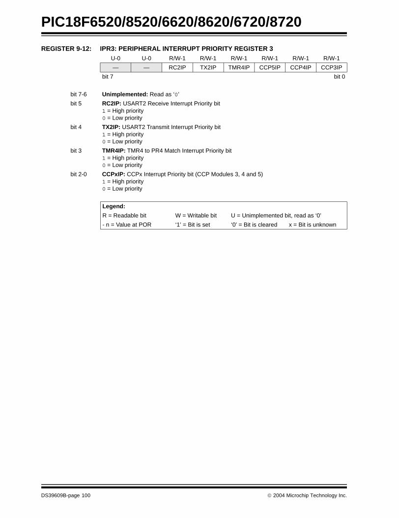
PIC18F6520/8520/6620/8620/6720/8720
REGISTER 9-12: IPR3: PERIPHERAL INTERRUPT PRIORITY REGISTER 3 U-0 U-0 R/W-1 R/W-1 R/W-1 R/W-1 R/W-1 R/W-1
— — RC2IP TX2IP TMR4IP CCP5IP CCP4IP CCP3IP
bit 7 bit 0
bit 7-6 Unimplemented: Read as ‘0’
bit 5 RC2IP: USART2 Receive Interrupt Priority bit 1 = High priority 0 = Low priority
bit 4 TX2IP: USART2 Transmit Interrupt Priority bit 1 = High priority 0 = Low priority
bit 3 TMR4IP: TMR4 to PR4 Match Interrupt Priority bit 1 = High priority 0 = Low priority
bit 2-0 CCPxIP: CCPx Interrupt Priority bit (CCP Modules 3, 4 and 5)1 = High priority 0 = Low priority
Legend:
R = Readable bit W = Writable bit U = Unimplemented bit, read as ‘0’
- n = Value at POR ‘1’ = Bit is set ‘0’ = Bit is cleared x = Bit is unknown
DS39609B-page 100 2004 Microchip Technology Inc.

PIC18F6520/8520/6620/8620/6720/8720
9.5 RCON Register
The RCON register contains the IPEN bit, which isused to enable prioritized interrupts. The functions ofthe other bits in this register are discussed in moredetail in Section 4.14 “RCON Register”.
REGISTER 9-13: RCON REGISTER R/W-0 U-0 U-0 R/W-1 R-1 R-1 R/W-0 R/W-0
IPEN — — RI TO PD POR BOR
bit 7 bit 0
bit 7 IPEN: Interrupt Priority Enable bit 1 = Enable priority levels on interrupts0 = Disable priority levels on interrupts (PIC16 Compatibility mode)
bit 6-5 Unimplemented: Read as ‘0’
bit 4 RI: RESET Instruction Flag bit For details of bit operation, see Register 4-4.
bit 3 TO: Watchdog Time-out Flag bit For details of bit operation, see Register 4-4.
bit 2 PD: Power-Down Detection Flag bit For details of bit operation, see Register 4-4.
bit 1 POR: Power-on Reset Status bitFor details of bit operation, see Register 4-4.
bit 0 BOR: Brown-out Reset Status bit For details of bit operation, see Register 4-4.
Legend:
R = Readable bit W = Writable bit U = Unimplemented bit, read as ‘0’
- n = Value at POR ‘1’ = Bit is set ‘0’ = Bit is cleared x = Bit is unknown
2004 Microchip Technology Inc. DS39609B-page 101
PIC18F6520/8520/6620/8620/6720/8720
9.6 INT0 Interrupt
External interrupts on the RB0/INT0, RB1/INT1,RB2/INT2 and RB3/INT3 pins are edge-triggered:either rising, if the corresponding INTEDGx bit is set inthe INTCON2 register, or falling, if the INTEDGx bit isclear. When a valid edge appears on the RBx/INTx pin,the corresponding flag bit, INTxF, is set. This interruptcan be disabled by clearing the corresponding enablebit, INTxE. Flag bit, INTxF, must be cleared in softwarein the Interrupt Service Routine before re-enabling theinterrupt. All external interrupts (INT0, INT1, INT2 andINT3) can wake-up the processor from Sleep if bitINTxIE was set prior to going into Sleep. If the GlobalInterrupt Enable bit, GIE, is set, the processor willbranch to the interrupt vector following wake-up.
The interrupt priority for INT, INT2 and INT3 is deter-mined by the value contained in the interrupt prioritybits: INT1IP (INTCON3<6>), INT2IP (INTCON3<7>)and INT3IP (INTCON2<1>). There is no priority bitassociated with INT0; it is always a high priorityinterrupt source.
9.7 TMR0 Interrupt
In 8-bit mode (which is the default), an overflow in theTMR0 register (FFh → 00h) will set flag bit TMR0IF. In16-bit mode, an overflow in the TMR0H:TMR0L regis-ters (FFFFh → 0000h) will set flag bit TMR0IF. Theinterrupt can be enabled/disabled by setting/clearingenable bit, TMR0IE (INTCON<5>). Interrupt priority forTimer0 is determined by the value contained in theinterrupt priority bit, TMR0IP (INTCON2<2>). SeeSection 11.0 “Timer0 Module” for further details onthe Timer0 module.
9.8 PORTB Interrupt-on-Change
An input change on PORTB<7:4> sets flag bit, RBIF(INTCON<0>). The interrupt can be enabled/disabledby setting/clearing enable bit, RBIE (INTCON<3>).Interrupt priority for PORTB interrupt-on-change isdetermined by the value contained in the interruptpriority bit, RBIP (INTCON2<0>).
9.9 Context Saving During Interrupts
During an interrupt, the return PC value is saved on thestack. Additionally, the WREG, Status and BSR registersare saved on the fast return stack. If a fast return frominterrupt is not used (see Section 4.3 “Fast RegisterStack”), the user may need to save the WREG, Statusand BSR registers in software. Depending on the user’sapplication, other registers may also need to be saved.Example 9-1 saves and restores the WREG, Status andBSR registers during an Interrupt Service Routine.
EXAMPLE 9-1: SAVING STATUS, WREG AND BSR REGISTERS IN RAM
MOVWF W_TEMP ; W_TEMP is in virtual bankMOVFF STATUS, STATUS_TEMP ; STATUS_TEMP located anywhereMOVFF BSR, BSR_TEMP ; BSR located anywhere;; USER ISR CODE;MOVFF BSR_TEMP, BSR ; Restore BSRMOVF W_TEMP, W ; Restore WREGMOVFF STATUS_TEMP, STATUS ; Restore STATUS
DS39609B-page 102 2004 Microchip Technology Inc.

PIC18F6520/8520/6620/8620/6720/8720
10.0 I/O PORTS
Depending on the device selected, there are eitherseven or nine I/O ports available on PIC18FXX20devices. Some of their pins are multiplexed with one ormore alternate functions from the other peripheral fea-tures on the device. In general, when a peripheral isenabled, that pin may not be used as a generalpurpose I/O pin.
Each port has three registers for its operation. Theseregisters are:
• TRIS register (data direction register)
• PORT register (reads the levels on the pins of the device)
• LAT register (output latch)
The Data Latch (LAT register) is useful for read-modify-write operations on the value that the I/O pins aredriving.
A simplified version of a generic I/O port and itsoperation is shown in Figure 10-1.
FIGURE 10-1: SIMPLIFIED BLOCK DIAGRAM OF PORT/LAT/TRIS OPERATION
10.1 PORTA, TRISA and LATA Registers
PORTA is a 7-bit wide, bidirectional port. The corre-sponding data direction register is TRISA. Setting aTRISA bit (= 1) will make the corresponding PORTA pinan input (i.e., put the corresponding output driver in ahigh-impedance mode). Clearing a TRISA bit (= 0) willmake the corresponding PORTA pin an output (i.e., putthe contents of the output latch on the selected pin).
Reading the PORTA register reads the status of thepins, whereas writing to it will write to the port latch.
The Data Latch register (LATA) is also memorymapped. Read-modify-write operations on the LATAregister, read and write the latched output value forPORTA.
The RA4 pin is multiplexed with the Timer0 moduleclock input to become the RA4/T0CKI pin. The RA4/T0CKI pin is a Schmitt Trigger input and an open-drainoutput. All other RA port pins have TTL input levels andfull CMOS output drivers.
The RA6 pin is only enabled as a general I/O pin inECIO and RCIO Oscillator modes.
The other PORTA pins are multiplexed with analoginputs and the analog VREF+ and VREF- inputs. Theoperation of each pin is selected by clearing/setting thecontrol bits in the ADCON1 register (A/D ControlRegister 1).
The TRISA register controls the direction of the RApins, even when they are being used as analog inputs.The user must ensure the bits in the TRISA register aremaintained set when using them as analog inputs.
EXAMPLE 10-1: INITIALIZING PORTA
QD
CK
WR LAT +
Data Latch
I/O pinRD Port
WR Port
TRIS
RD LAT
Data Bus
Note: On a Power-on Reset, RA5 and RA3:RA0are configured as analog inputs and readas ‘0’. RA6 and RA4 are configured asdigital inputs.
CLRF PORTA ; Initialize PORTA by; clearing output; data latches
CLRF LATA ; Alternate method; to clear output; data latches
MOVLW 0x0F ; Configure A/D MOVWF ADCON1 ; for digital inputsMOVLW 0xCF ; Value used to
; initialize data ; direction
MOVWF TRISA ; Set RA<3:0> as inputs; RA<5:4> as outputs
2004 Microchip Technology Inc. DS39609B-page 103

PIC18F6520/8520/6620/8620/6720/8720
FIGURE 10-2: BLOCK DIAGRAM OF RA3:RA0 AND RA5 PINS
FIGURE 10-3: BLOCK DIAGRAM OF RA4/T0CKI PIN
FIGURE 10-4: BLOCK DIAGRAM OF RA6 PIN (WHEN ENABLED AS I/O)
DataBus
QD
QCK
QD
QCK
Q D
EN
P
N
WR LATA
WR TRISA
Data Latch
TRIS Latch
RD TRISA
RD PORTA
VSS
VDD
I/O pin(1)
Note 1: I/O pins have protection diodes to VDD and VSS.
AnalogInputMode
TTLInputBuffer
To A/D Converter and LVD Modules
RD LATA
orPORTA
DataBus
WR TRISA
RD PORTA
Data Latch
TRIS Latch
SchmittTriggerInputBuffer
N
VSS
I/O pin(1)
TMR0 Clock Input
QD
QCK
QD
QCK
EN
Q D
EN
RD LATA
WR LATAorPORTA
Note 1: I/O pins have protection diodes to VDD and VSS.
RD TRISA
Data Bus
QD
QCK
Q D
EN
P
N
WR LATA
WR
Data Latch
TRIS Latch
RD
RD PORTA
VSS
VDD
I/O pin(1)
Note 1: I/O pins have protection diodes to VDD and VSS.
or PORTA
RD LATA
ECRA6 or
TTLInputBuffer
ECRA6 or RCRA6 Enable
RCRA6 Enable
TRISA
QD
QCK
TRISA
DS39609B-page 104 2004 Microchip Technology Inc.

PIC18F6520/8520/6620/8620/6720/8720
TABLE 10-1: PORTA FUNCTIONS
TABLE 10-2: SUMMARY OF REGISTERS ASSOCIATED WITH PORTA
Name Bit# Buffer Function
RA0/AN0 bit 0 TTL Input/output or analog input.
RA1/AN1 bit 1 TTL Input/output or analog input.
RA2/AN2/VREF- bit 2 TTL Input/output or analog input or VREF-.
RA3/AN3/VREF+ bit 3 TTL Input/output or analog input or VREF+.
RA4/T0CKI bit 4 ST Input/output or external clock input for Timer0.Output is open-drain type.
RA5/AN4/LVDIN bit 5 TTL Input/output or slave select input for synchronous serial port or analog input, or Low-Voltage Detect input.
OSC2/CLKO/RA6 bit 6 TTL OSC2 or clock output, or I/O pin.
Legend: TTL = TTL input, ST = Schmitt Trigger input
Name Bit 7 Bit 6 Bit 5 Bit 4 Bit 3 Bit 2 Bit 1 Bit 0Value on
POR, BOR
Value on all other Resets
PORTA — RA6 RA5 RA4 RA3 RA2 RA1 RA0 -x0x 0000 -u0u 0000
LATA — LATA Data Output Register -xxx xxxx -uuu uuuu
TRISA — PORTA Data Direction Register -111 1111 -111 1111
ADCON1 — — VCFG1 VCFG0 PCFG3 PCFG2 PCFG1 PCFG0 --00 0000 --00 0000
Legend: x = unknown, u = unchanged, – = unimplemented locations read as ‘0’. Shaded cells are not used by PORTA.
2004 Microchip Technology Inc. DS39609B-page 105
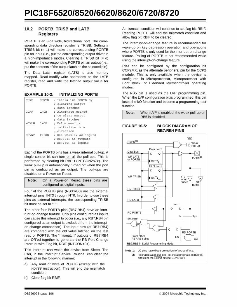
PIC18F6520/8520/6620/8620/6720/8720
10.2 PORTB, TRISB and LATB Registers
PORTB is an 8-bit wide, bidirectional port. The corre-sponding data direction register is TRISB. Setting aTRISB bit (= 1) will make the corresponding PORTBpin an input (i.e., put the corresponding output driver ina high-impedance mode). Clearing a TRISB bit (= 0)will make the corresponding PORTB pin an output (i.e.,put the contents of the output latch on the selected pin).
The Data Latch register (LATB) is also memorymapped. Read-modify-write operations on the LATBregister, read and write the latched output value forPORTB.
EXAMPLE 10-2: INITIALIZING PORTB
Each of the PORTB pins has a weak internal pull-up. Asingle control bit can turn on all the pull-ups. This isperformed by clearing bit RBPU (INTCON2<7>). Theweak pull-up is automatically turned off when the portpin is configured as an output. The pull-ups aredisabled on a Power-on Reset.
Four of the PORTB pins (RB3:RB0) are the externalinterrupt pins, INT3 through INT0. In order to use thesepins as external interrupts, the corresponding TRISBbit must be set to ‘1’.
The other four PORTB pins (RB7:RB4) have an inter-rupt-on-change feature. Only pins configured as inputscan cause this interrupt to occur (i.e., any RB7:RB4 pinconfigured as an output is excluded from the interrupt-on-change comparison). The input pins (of RB7:RB4)are compared with the old value latched on the lastread of PORTB. The “mismatch” outputs of RB7:RB4are OR’ed together to generate the RB Port ChangeInterrupt with Flag bit, RBIF (INTCON<0>).
This interrupt can wake the device from Sleep. Theuser, in the Interrupt Service Routine, can clear theinterrupt in the following manner:
a) Any read or write of PORTB (except with theMOVFF instruction). This will end the mismatchcondition.
b) Clear flag bit RBIF.
A mismatch condition will continue to set flag bit, RBIF.Reading PORTB will end the mismatch condition andallow flag bit RBIF to be cleared.
The interrupt-on-change feature is recommended forwake-up on key depression operation and operationswhere PORTB is only used for the interrupt-on-changefeature. Polling of PORTB is not recommended whileusing the interrupt-on-change feature.
RB3 can be configured by the configuration bitCCP2MX, as the alternate peripheral pin for the CCP2module. This is only available when the device isconfigured in Microprocessor, Microprocessor withBoot Block, or Extended Microcontroller operatingmodes.
The RB5 pin is used as the LVP programming pin.When the LVP configuration bit is programmed, this pinloses the I/O function and become a programming testfunction.
FIGURE 10-5: BLOCK DIAGRAM OFRB7:RB4 PINS
Note: On a Power-on Reset, these pins areconfigured as digital inputs.
CLRF PORTB ; Initialize PORTB by; clearing output; data latches
CLRF LATB ; Alternate method; to clear output; data latches
MOVLW 0xCF ; Value used to; initialize data ; direction
MOVWF TRISB ; Set RB<3:0> as inputs; RB<5:4> as outputs; RB<7:6> as inputs
Note: When LVP is enabled, the weak pull-up onRB5 is disabled.
Data Latch
From other
RBPU(2)
P
VDD
I/O pin(1)QD
CK
QD
CK
Q D
EN
Q D
EN
Data Bus
WR LATB
WR TRISB
Set RBIF
TRIS Latch
RD TRISB
RD PORTB
RB7:RB4 pins
WeakPull-up
RD PORTB
Latch
TTLInputBuffer ST
Buffer
RB7:RB5 in Serial Programming Mode
Q3
Q1
RD LATB
or PORTB
Note 1: I/O pins have diode protection to VDD and VSS.
2: To enable weak pull-ups, set the appropriate TRIS bit(s)and clear the RBPU bit (INTCON2<7>).
DS39609B-page 106 2004 Microchip Technology Inc.

PIC18F6520/8520/6620/8620/6720/8720
FIGURE 10-6: BLOCK DIAGRAM OF RB2:RB0 PINS
FIGURE 10-7: BLOCK DIAGRAM OF RB3 PIN
Data Latch
RBPU(2)
P
VDD
QD
CK
QD
CK
Q D
EN
Data Bus
WR Port
WR TRIS
RD TRIS
RD Port
WeakPull-up
RD Port
INTx
I/O pin(1)
TTLInputBuffer
Schmitt TriggerBuffer
TRIS Latch
Note 1: I/O pins have diode protection to VDD and VSS.
2: To enable weak pull-ups, set the appropriate TRIS bit(s) and clear the RBPU bit (OPTION_REG<7>).
Data Latch
P
VDD
QD
CK
Q D
EN
Data Bus
WR LATB or
WR TRISB
RD TRISB
RD PORTB
WeakPull-up
CCP2 or INT3
TTLInputBuffer
Schmitt TriggerBuffer
TRIS Latch
RD LATB
WR PORTB
RBPU(2)
CK
D
Enable(3) CCP Output
RD PORTB
CCP Output(3)1
0
P
N
VDD
VSS
I/O pin(1)
Q
CCP2MX
CCP2MX = 0
Note 1: I/O pin has diode protection to VDD and VSS.
2: To enable weak pull-ups, set the appropriate TRIS bit(s) and clear the RBPU bit (INTCON2<7>).
3: The CCP2 input/output is multiplexed with RB3 if the CCP2MX bit is enabled (= 0) in the Configuration register and the deviceis operating in Microprocessor, Microprocessor with Boot Block or Extended Microcontroller mode.
2004 Microchip Technology Inc. DS39609B-page 107

PIC18F6520/8520/6620/8620/6720/8720
TABLE 10-3: PORTB FUNCTIONS
TABLE 10-4: SUMMARY OF REGISTERS ASSOCIATED WITH PORTB
Name Bit# Buffer Function
RB0/INT0 bit 0 TTL/ST(1) Input/output pin or external interrupt input 0.Internal software programmable weak pull-up.
RB1/INT1 bit 1 TTL/ST(1) Input/output pin or external interrupt input 1. Internal software programmable weak pull-up.
RB2/INT2 bit 2 TTL/ST(1) Input/output pin or external interrupt input 2. Internal software programmable weak pull-up.
RB3/INT3/CCP2(3) bit 3 TTL/ST(4) Input/output pin or external interrupt input 3. Capture2 input/Compare2 output/PWM output (when CCP2MX configuration bit is enabled, all PIC18F8X20 operating modes except Microcontroller mode). Internal software programmable weak pull-up.
RB4/KBI0 bit 4 TTL Input/output pin (with interrupt-on-change). Internal software programmable weak pull-up.
RB5/KBI1/PGM bit 5 TTL/ST(2) Input/output pin (with interrupt-on-change). Internal software programmable weak pull-up.Low-voltage ICSP enable pin.
RB6/KBI2/PGC bit 6 TTL/ST(2) Input/output pin (with interrupt-on-change). Internal software programmable weak pull-up. Serial programming clock.
RB7/KBI3/PGD bit 7 TTL/ST(2) Input/output pin (with interrupt-on-change). Internal software programmable weak pull-up. Serial programming data.
Legend: TTL = TTL input, ST = Schmitt Trigger input
Note 1: This buffer is a Schmitt Trigger input when configured as the external interrupt.2: This buffer is a Schmitt Trigger input when used in Serial Programming mode.3: RC1 is the alternate assignment for CCP2 when CCP2MX is not set (all operating modes except
Microcontroller mode).4: This buffer is a Schmitt Trigger input when configured as the CCP2 input.
Name Bit 7 Bit 6 Bit 5 Bit 4 Bit 3 Bit 2 Bit 1 Bit 0Value on
POR, BOR
Value on all other Resets
PORTB RB7 RB6 RB5 RB4 RB3 RB2 RB1 RB0 xxxx xxxx uuuu uuuu
LATB LATB Data Output Register xxxx xxxx uuuu uuuu
TRISB PORTB Data Direction Register 1111 1111 1111 1111
INTCON GIE/GIEH
PEIE/GIEL
TMR0IE INT0IE RBIE TMR0IF INT0IF RBIF 0000 0000 0000 0000
INTCON2 RBPU INTEDG0 INTEDG1 INTEDG2 INTEDG3 TMR0IP INT3IP RBIP 1111 1111 1111 1111
INTCON3 INT2IP INT1IP INT3IE INT2IE INT1IE INT3IF INT2IF INT1IF 1100 0000 1100 0000
Legend: x = unknown, u = unchanged. Shaded cells are not used by PORTB.
DS39609B-page 108 2004 Microchip Technology Inc.

PIC18F6520/8520/6620/8620/6720/8720
10.3 PORTC, TRISC and LATC Registers
PORTC is an 8-bit wide, bidirectional port. The corre-sponding data direction register is TRISC. Setting aTRISC bit (= 1) will make the corresponding PORTCpin an input (i.e., put the corresponding output driver ina high-impedance mode). Clearing a TRISC bit (= 0)will make the corresponding PORTC pin an output (i.e.,put the contents of the output latch on the selected pin).
The Data Latch register (LATC) is also memorymapped. Read-modify-write operations on the LATCregister, read and write the latched output value forPORTC.
PORTC is multiplexed with several peripheral functions(Table 10-5). PORTC pins have Schmitt Trigger inputbuffers.
When enabling peripheral functions, care should betaken in defining TRIS bits for each PORTC pin. Someperipherals override the TRIS bit to make a pin anoutput, while other peripherals override the TRIS bit tomake a pin an input. The user should refer to thecorresponding peripheral section for the correct TRISbit settings.
The pin override value is not loaded into the TRISregister. This allows read-modify-write of the TRISregister, without concern due to peripheral overrides.
RC1 is normally configured by configuration bit,CCP2MX, as the default peripheral pin of the CCP2module (default/erased state, CCP2MX = 1).
EXAMPLE 10-3: INITIALIZING PORTC
FIGURE 10-8: PORTC BLOCK DIAGRAM (PERIPHERAL OUTPUT OVERRIDE)
Note: On a Power-on Reset, these pins areconfigured as digital inputs.
CLRF PORTC ; Initialize PORTC by; clearing output; data latches
CLRF LATC ; Alternate method; to clear output; data latches
MOVLW 0xCF ; Value used to ; initialize data ; direction
MOVWF TRISC ; Set RC<3:0> as inputs; RC<5:4> as outputs; RC<7:6> as inputs
PORTC/Peripheral Out Select
Data Bus
WR LATC
WR TRISC
Data Latch
TRIS Latch
RD TRISC
QD
QCK
Q D
EN
Peripheral Data Out0
1
QD
QCK
P
N
VDD
VSS
RD PORTC
Peripheral Data In
I/O pin(1)orWR PORTC
RD LATC
SchmittTrigger
Note 1: I/O pins have diode protection to VDD and VSS.
2: Peripheral Output Enable is only active if Peripheral Select is active.
TRISOverride
Peripheral Output
Logic
TRIS OVERRIDE
Pin Override Peripheral
RC0 Yes Timer1 Osc for Timer1/Timer3
RC1 Yes Timer1 Osc for Timer1/Timer3,
CCP2 I/O
RC2 Yes CCP1 I/O
RC3 Yes SPI/I2C Master Clock
RC4 Yes I2C Data Out
RC5 Yes SPI Data Out
RC6 Yes USART1 Async Xmit, Sync Clock
RC7 Yes USART1 Sync Data Out
Enable(2)
2004 Microchip Technology Inc. DS39609B-page 109
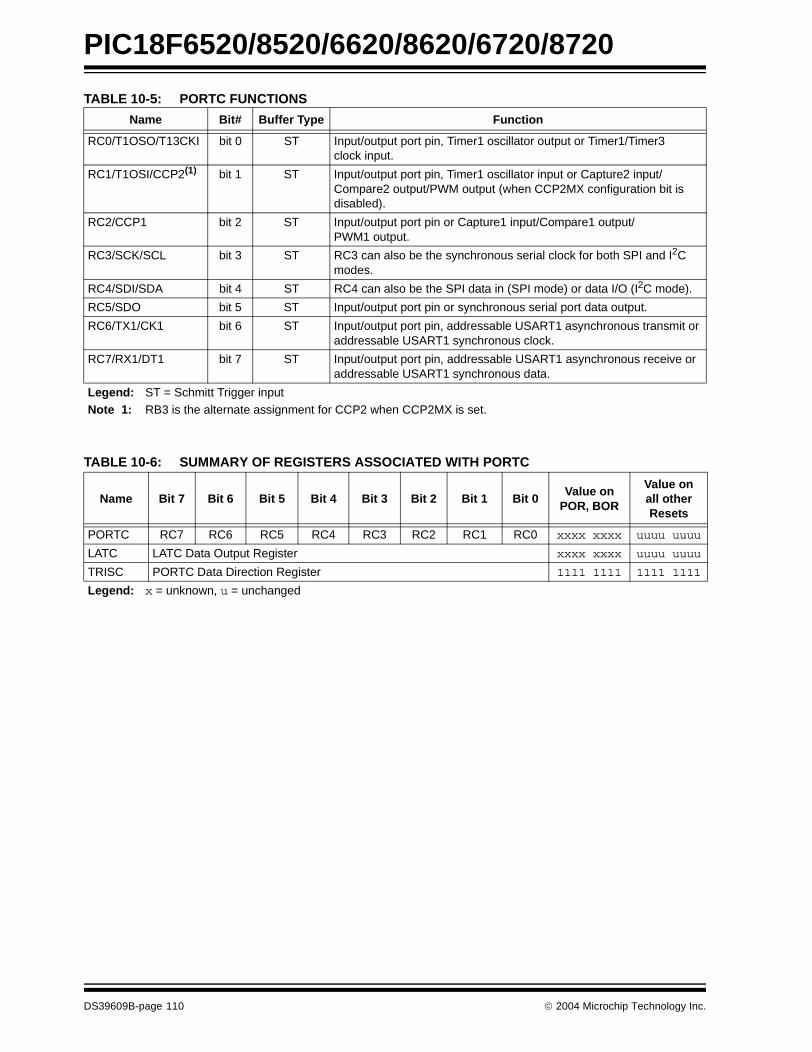
PIC18F6520/8520/6620/8620/6720/8720
TABLE 10-5: PORTC FUNCTIONS
TABLE 10-6: SUMMARY OF REGISTERS ASSOCIATED WITH PORTC
Name Bit# Buffer Type Function
RC0/T1OSO/T13CKI bit 0 ST Input/output port pin, Timer1 oscillator output or Timer1/Timer3clock input.
RC1/T1OSI/CCP2(1) bit 1 ST Input/output port pin, Timer1 oscillator input or Capture2 input/ Compare2 output/PWM output (when CCP2MX configuration bit is disabled).
RC2/CCP1 bit 2 ST Input/output port pin or Capture1 input/Compare1 output/PWM1 output.
RC3/SCK/SCL bit 3 ST RC3 can also be the synchronous serial clock for both SPI and I2C modes.
RC4/SDI/SDA bit 4 ST RC4 can also be the SPI data in (SPI mode) or data I/O (I2C mode).
RC5/SDO bit 5 ST Input/output port pin or synchronous serial port data output.
RC6/TX1/CK1 bit 6 ST Input/output port pin, addressable USART1 asynchronous transmit or addressable USART1 synchronous clock.
RC7/RX1/DT1 bit 7 ST Input/output port pin, addressable USART1 asynchronous receive or addressable USART1 synchronous data.
Legend: ST = Schmitt Trigger inputNote 1: RB3 is the alternate assignment for CCP2 when CCP2MX is set.
Name Bit 7 Bit 6 Bit 5 Bit 4 Bit 3 Bit 2 Bit 1 Bit 0Value on
POR, BOR
Value on all other Resets
PORTC RC7 RC6 RC5 RC4 RC3 RC2 RC1 RC0 xxxx xxxx uuuu uuuu
LATC LATC Data Output Register xxxx xxxx uuuu uuuu
TRISC PORTC Data Direction Register 1111 1111 1111 1111
Legend: x = unknown, u = unchanged
DS39609B-page 110 2004 Microchip Technology Inc.

PIC18F6520/8520/6620/8620/6720/8720
10.4 PORTD, TRISD and LATD Registers
PORTD is an 8-bit wide, bidirectional port. The corre-sponding data direction register is TRISD. Setting aTRISD bit (= 1) will make the corresponding PORTDpin an input (i.e., put the corresponding output driver ina high-impedance mode). Clearing a TRISD bit (= 0)will make the corresponding PORTD pin an output (i.e.,put the contents of the output latch on the selected pin).
The Data Latch register (LATD) is also memorymapped. Read-modify-write operations on the LATDregister, read and write the latched output value forPORTD.
PORTD is an 8-bit port with Schmitt Trigger input buff-ers. Each pin is individually configurable as an input oroutput.
PORTD is multiplexed with the system bus as theexternal memory interface; I/O port functions are onlyavailable when the system bus is disabled, by settingthe EBDIS bit in the MEMCOM register(MEMCON<7>). When operating as the external mem-ory interface, PORTD is the low-order byte of themultiplexed address/data bus (AD7:AD0).
PORTD can also be configured as an 8-bit wide micro-processor port (Parallel Slave Port) by setting controlbit PSPMODE (TRISE<4>). In this mode, the inputbuffers are TTL. See Section 10.10 “Parallel SlavePort” for additional information on the Parallel SlavePort (PSP).
EXAMPLE 10-4: INITIALIZING PORTD
FIGURE 10-9: PORTD BLOCK DIAGRAM IN I/O PORT MODE
Note: On a Power-on Reset, these pins areconfigured as digital inputs.
CLRF PORTD ; Initialize PORTD by ; clearing output ; data latchesCLRF LATD ; Alternate method
; to clear output; data latches
MOVLW 0xCF ; Value used to ; initialize data ; direction
MOVWF TRISD ; Set RD<3:0> as inputs; RD<5:4> as outputs; RD<7:6> as inputs
Data Bus
WR LATD
WR TRISD
Data Latch
TRIS Latch
RD TRISD
I/O pin(1)
QD
CK
QD
CK
EN
Q D
EN
RD LATD
or PORTD
0
1
Q
Q 0
1
P
N
VDD
VSS
0
1
RD PORTD
PSP Read
PSP Write
Note 1: I/O pins have diode protection to VDD and VSS.
TTL Buffer
Schmitt TriggerInput Buffer
PORTD/CCP1 Select
PSPMODE
2004 Microchip Technology Inc. DS39609B-page 111

PIC18F6520/8520/6620/8620/6720/8720
FIGURE 10-10: PORTD BLOCK DIAGRAM IN SYSTEM BUS MODE
Instruction Register
Bus Enable
Data/TRIS Out
Drive Bus
System BusControl
Data Bus
WR LATD
WR TRISD
RD PORTD
Data Latch
TRIS Latch
RD TRISD
TTLInputBuffer
I/O pin(1)
QD
CK
QD
CK
EN
Q D
EN
RD LATD
or PORTD
0
1
Port
Data
Instruction Read
Note 1: I/O pins have protection diodes to VDD and VSS.
DS39609B-page 112 2004 Microchip Technology Inc.

PIC18F6520/8520/6620/8620/6720/8720
TABLE 10-7: PORTD FUNCTIONS
TABLE 10-8: SUMMARY OF REGISTERS ASSOCIATED WITH PORTD
Name Bit# Buffer Type Function
RD0/PSP0/AD0 bit 0 ST/TTL(1) Input/output port pin, Parallel Slave Port bit 0 or address/data bus bit 0.
RD1/PSP1/AD1 bit 1 ST/TTL(1) Input/output port pin, Parallel Slave Port bit 1 or address/data bus bit 1.
RD2/PSP2/AD2 bit 2 ST/TTL(1) Input/output port pin, Parallel Slave Port bit 2 or address/data bus bit 2.
RD3/PSP3/AD3 bit 3 ST/TTL(1) Input/output port pin, Parallel Slave Port bit 3 or address/data bus bit 3.
RD4/PSP4/AD4 bit 4 ST/TTL(1) Input/output port pin, Parallel Slave Port bit 4 or address/data bus bit 4.
RD5/PSP5/AD5 bit 5 ST/TTL(1) Input/output port pin, Parallel Slave Port bit 5 or address/data bus bit 5.
RD6/PSP6/AD6 bit 6 ST/TTL(1) Input/output port pin, Parallel Slave Port bit 6 or address/data bus bit 6.
RD7/PSP7/AD7 bit 7 ST/TTL(1) Input/output port pin, Parallel Slave Port bit 7 or address/data bus bit 7.
Legend: ST = Schmitt Trigger input, TTL = TTL input Note 1: Input buffers are Schmitt Triggers when in I/O mode and TTL buffers when in System Bus or Parallel
Slave Port mode.
Name Bit 7 Bit 6 Bit 5 Bit 4 Bit 3 Bit 2 Bit 1 Bit 0Value on
POR, BOR
Value on all other Resets
PORTD RD7 RD6 RD5 RD4 RD3 RD2 RD1 RD0 xxxx xxxx uuuu uuuu
LATD LATD Data Output Register xxxx xxxx uuuu uuuu
TRISD PORTD Data Direction Register 1111 1111 1111 1111
PSPCON IBF OBF IBOV PSPMODE — — — — 0000 ---- 0000 ----
MEMCON EBDIS — WAIT1 WAIT0 — — WM1 WM0 0-00 --00 0-00 --00
Legend: x = unknown, u = unchanged, – = unimplemented, read as ‘0’. Shaded cells are not used by PORTD.
2004 Microchip Technology Inc. DS39609B-page 113
PIC18F6520/8520/6620/8620/6720/8720
10.5 PORTE, TRISE and LATE Registers
PORTE is an 8-bit wide, bidirectional port. The corre-sponding data direction register is TRISE. Setting aTRISE bit (= 1) will make the corresponding PORTEpin an input (i.e., put the corresponding output driver ina high-impedance mode). Clearing a TRISE bit (= 0)will make the corresponding PORTE pin an output (i.e.,put the contents of the output latch on the selected pin).
Read-modify-write operations on the LATE register,read and write the latched output value for PORTE.
PORTE is an 8-bit port with Schmitt Trigger input buff-ers. Each pin is individually configurable as an input oroutput. PORTE is multiplexed with the CCP module(Table 10-9).
On PIC18F8X20 devices, PORTE is also multiplexedwith the system bus as the external memory interface;the I/O bus is available only when the system bus isdisabled, by setting the EBDIS bit in the MEMCONregister (MEMCON<7>). If the device is configured inMicroprocessor or Extended Microcontroller mode,then the PORTE<7:0> becomes the high byte of theaddress/data bus for the external program memoryinterface. In Microcontroller mode, the PORTE<2:0>pins become the control inputs for the Parallel SlavePort when bit PSPMODE (PSPCON<4>) is set. (Referto Section 4.1.1 “PIC18F8X20 Program MemoryModes” for more information on program memorymodes.)
When the Parallel Slave Port is active, three PORTEpins (RE0/RD/AD8, RE1/WR/AD9 and RE2/CS/AD10)function as its control inputs. This automatically occurswhen the PSPMODE bit (PSPCON<4>) is set. Usersmust also make certain that bits TRISE<2:0> are set toconfigure the pins as digital inputs and the ADCON1register is configured for digital I/O. The PORTE PSPcontrol functions are summarized in Table 10-9.
Pin RE7 can be configured as the alternate peripheralpin for CCP module 2 when the device is operating inMicrocontroller mode. This is done by clearing theconfiguration bit, CCP2MX, in configuration register,CONFIG3H (CONFIG3H<0>).
EXAMPLE 10-5: INITIALIZING PORTE
Note: For PIC18F8X20 (80-pin) devices operat-ing in Extended Microcontroller mode,PORTE defaults to the system bus onPower-on Reset.
CLRF PORTE ; Initialize PORTE by; clearing output; data latches
CLRF LATE ; Alternate method; to clear output; data latches
MOVLW 0x03 ; Value used to ; initialize data ; direction
MOVWF TRISE ; Set RE1:RE0 as inputs; RE7:RE2 as outputs
DS39609B-page 114 2004 Microchip Technology Inc.
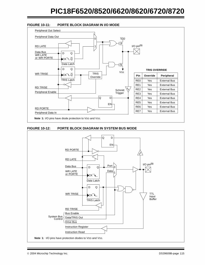
PIC18F6520/8520/6620/8620/6720/8720
FIGURE 10-11: PORTE BLOCK DIAGRAM IN I/O MODE
FIGURE 10-12: PORTE BLOCK DIAGRAM IN SYSTEM BUS MODE
Peripheral Out Select
Data BusWR LATE
WR TRISE
Data Latch
TRIS Latch
RD TRISE
QD
QCK
Q D
EN
Peripheral Data Out0
1
QD
QCK
P
N
VDD
VSS
RD PORTE
Peripheral Data In
I/O pin(1)
or WR PORTE
RD LATE
SchmittTrigger
Note 1: I/O pins have diode protection to VDD and VSS.
TRISOverride
Peripheral Enable
TRIS OVERRIDE
Pin Override Peripheral
RE0 Yes External Bus
RE1 Yes External Bus
RE2 Yes External Bus
RE3 Yes External Bus
RE4 Yes External Bus
RE5 Yes External Bus
RE6 Yes External Bus
RE7 Yes External Bus
Instruction Register
Bus Enable
Data/TRIS Out
Drive Bus
System BusControl
Data Bus
WR LATE
WR TRISE
RD PORTE
Data Latch
TRIS Latch
RD TRISE
TTLInputBuffer
I/O pin(1)
QD
CK
QD
CK
EN
Q D
EN
RD LATE
or PORTE
0
1
Port
Data
Instruction Read
Note 1: I/O pins have protection diodes to VDD and VSS.
2004 Microchip Technology Inc. DS39609B-page 115
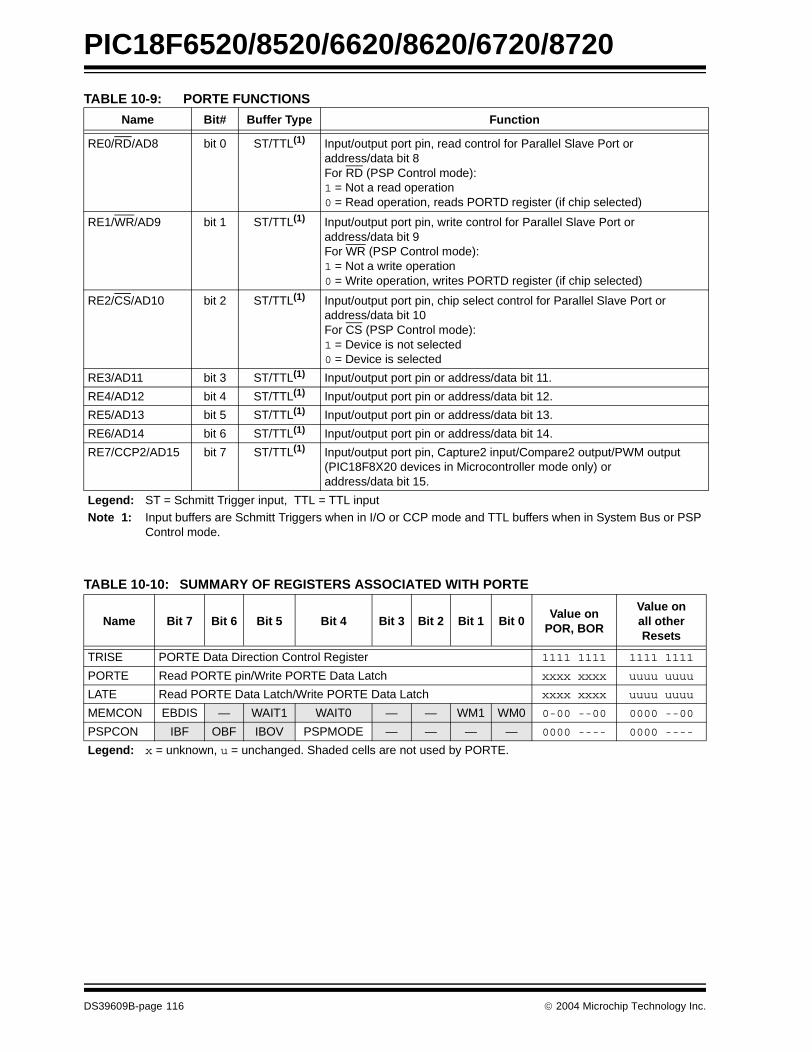
PIC18F6520/8520/6620/8620/6720/8720
TABLE 10-9: PORTE FUNCTIONS
TABLE 10-10: SUMMARY OF REGISTERS ASSOCIATED WITH PORTE
Name Bit# Buffer Type Function
RE0/RD/AD8 bit 0 ST/TTL(1) Input/output port pin, read control for Parallel Slave Port or address/data bit 8For RD (PSP Control mode):1 = Not a read operation0 = Read operation, reads PORTD register (if chip selected)
RE1/WR/AD9 bit 1 ST/TTL(1) Input/output port pin, write control for Parallel Slave Port or address/data bit 9For WR (PSP Control mode):1 = Not a write operation0 = Write operation, writes PORTD register (if chip selected)
RE2/CS/AD10 bit 2 ST/TTL(1) Input/output port pin, chip select control for Parallel Slave Port or address/data bit 10For CS (PSP Control mode):1 = Device is not selected0 = Device is selected
RE3/AD11 bit 3 ST/TTL(1) Input/output port pin or address/data bit 11.
RE4/AD12 bit 4 ST/TTL(1) Input/output port pin or address/data bit 12.
RE5/AD13 bit 5 ST/TTL(1) Input/output port pin or address/data bit 13.
RE6/AD14 bit 6 ST/TTL(1) Input/output port pin or address/data bit 14.
RE7/CCP2/AD15 bit 7 ST/TTL(1) Input/output port pin, Capture2 input/Compare2 output/PWM output (PIC18F8X20 devices in Microcontroller mode only) or address/data bit 15.
Legend: ST = Schmitt Trigger input, TTL = TTL inputNote 1: Input buffers are Schmitt Triggers when in I/O or CCP mode and TTL buffers when in System Bus or PSP
Control mode.
Name Bit 7 Bit 6 Bit 5 Bit 4 Bit 3 Bit 2 Bit 1 Bit 0Value on
POR, BOR
Value on all other Resets
TRISE PORTE Data Direction Control Register 1111 1111 1111 1111
PORTE Read PORTE pin/Write PORTE Data Latch xxxx xxxx uuuu uuuu
LATE Read PORTE Data Latch/Write PORTE Data Latch xxxx xxxx uuuu uuuu
MEMCON EBDIS — WAIT1 WAIT0 — — WM1 WM0 0-00 --00 0000 --00
PSPCON IBF OBF IBOV PSPMODE — — — — 0000 ---- 0000 ----
Legend: x = unknown, u = unchanged. Shaded cells are not used by PORTE.
DS39609B-page 116 2004 Microchip Technology Inc.

PIC18F6520/8520/6620/8620/6720/8720
10.6 PORTF, LATF and TRISF Registers
PORTF is an 8-bit wide, bidirectional port. The corre-sponding data direction register is TRISF. Setting aTRISF bit (= 1) will make the corresponding PORTF pinan input (i.e., put the corresponding output driver in ahigh-impedance mode). Clearing a TRISF bit (= 0) willmake the corresponding PORTF pin an output (i.e., putthe contents of the output latch on the selected pin).
Read-modify-write operations on the LATF register,read and write the latched output value for PORTF.
PORTF is multiplexed with several analog peripheralfunctions, including the A/D converter inputs andcomparator inputs, outputs and voltage reference.
EXAMPLE 10-6: INITIALIZING PORTF
FIGURE 10-13: PORTF RF1/AN6/C2OUT, RF2/AN7/C1OUT PINS BLOCK DIAGRAM
Note 1: On a Power-on Reset, the RF6:RF0 pinsare configured as inputs and read as ‘0’.
2: To configure PORTF as digital I/O, turn offcomparators and set ADCON1 value.
CLRF PORTF ; Initialize PORTF by ; clearing output ; data latches
CLRF LATF ; Alternate method ; to clear output ; data latches
MOVLW 0x07 ; MOVWF CMCON ; Turn off comparatorsMOVLW 0x0F ; MOVWF ADCON1 ; Set PORTF as digital I/OMOVLW 0xCF ; Value used to
; initialize data; direction
MOVWF TRISF ; Set RF3:RF0 as inputs; RF5:RF4 as outputs; RF7:RF6 as inputs
Port/Comparator Select
Data Bus
WR LATF
WR TRISF
Data Latch
TRIS Latch
RD TRISF
QD
QCK
Q D
EN
Comparator Data Out0
1
QD
QCK
P
N
VDD
VSS
RD PORTF
I/O pinorWR PORTF
RD LATF
SchmittTrigger
Note 1: I/O pins have diode protection to VDD and VSS.
AnalogInputMode
To A/D Converter
2004 Microchip Technology Inc. DS39609B-page 117

PIC18F6520/8520/6620/8620/6720/8720
FIGURE 10-14: RF6:RF3 AND RF0 PINS BLOCK DIAGRAM
FIGURE 10-15: RF7 PIN BLOCK DIAGRAM
DataBus
QD
QCK
QD
QCK
Q D
EN
P
N
WR LATF
WR TRISF
Data Latch
TRIS Latch
RD TRISF
RD PORTF
VSS
VDD
I/O pin
AnalogInputMode
STInputBuffer
To A/D Converter or Comparator Input
RD LATF
orWR PORTF
Note 1: I/O pins have diode protection to VDD and VSS.
DataBus
WR LATF
WR TRISF
RD PORTF
Data Latch
TRIS Latch
RD TRISF
SchmittTriggerInputBuffer
I/O pin
QD
CK
QD
CK
EN
Q D
EN
RD LATF
orWR PORTF
Note: I/O pins have diode protection to VDD and VSS.
TTLInputBuffer
SS Input
DS39609B-page 118 2004 Microchip Technology Inc.

PIC18F6520/8520/6620/8620/6720/8720
TABLE 10-11: PORTF FUNCTIONS
TABLE 10-12: SUMMARY OF REGISTERS ASSOCIATED WITH PORTF
Name Bit# Buffer Type Function
RF0/AN5 bit 0 ST Input/output port pin or analog input.
RF1/AN6/C2OUT bit 1 ST Input/output port pin, analog input or comparator 2 output.
RF2/AN7/C1OUT bit 2 ST Input/output port pin, analog input or comparator 1 output.
RF3/AN8 bit 3 ST Input/output port pin or analog input/comparator input.
RF4/AN9 bit 4 ST Input/output port pin or analog input/comparator input.
RF5/AN10/CVREF bit 5 ST Input/output port pin, analog input/comparator input or comparator reference output.
RF6/AN11 bit 6 ST Input/output port pin or analog input/comparator input.
RF7/SS bit 7 ST/TTL Input/output port pin or slave select pin for synchronous serial port.
Legend: ST = Schmitt Trigger input, TTL = TTL input
Name Bit 7 Bit 6 Bit 5 Bit 4 Bit 3 Bit 2 Bit 1 Bit 0Value on
POR, BOR
Value on all other Resets
TRISF PORTF Data Direction Control Register 1111 1111 1111 1111
PORTF Read PORTF pin/Write PORTF Data Latch xxxx xxxx uuuu uuuu
LATF Read PORTF Data Latch/Write PORTF Data Latch 0000 0000 uuuu uuuu
ADCON1 — — VCFG1 VCFG0 PCFG3 PCFG2 PCFG1 PCFG0 --00 0000 --00 0000
CMCON C2OUT C1OUT C2INV C1INV CIS CM2 CM1 CM0 0000 0000 0000 0000
CVRCON CVREN CVROE CVRR CVRSS CVR3 CVR2 CVR1 CVR0 0000 0000 0000 0000
Legend: x = unknown, u = unchanged. Shaded cells are not used by PORTF.
2004 Microchip Technology Inc. DS39609B-page 119
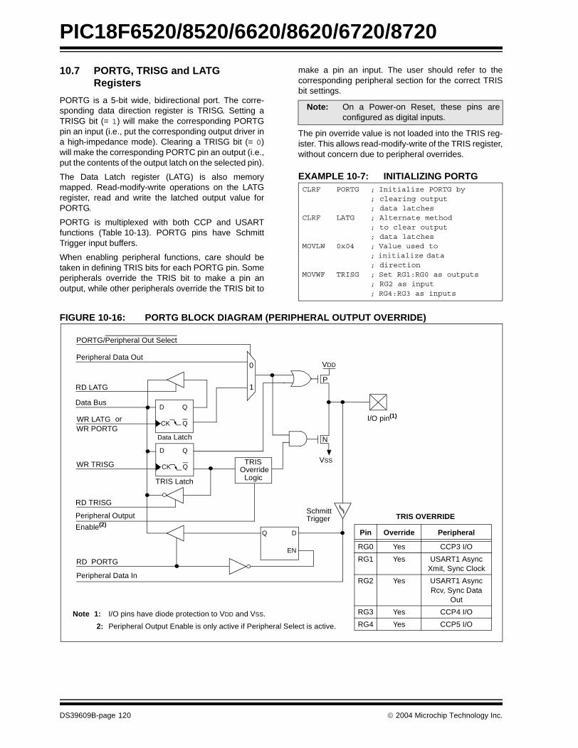
PIC18F6520/8520/6620/8620/6720/8720
10.7 PORTG, TRISG and LATG Registers
PORTG is a 5-bit wide, bidirectional port. The corre-sponding data direction register is TRISG. Setting aTRISG bit (= 1) will make the corresponding PORTGpin an input (i.e., put the corresponding output driver ina high-impedance mode). Clearing a TRISG bit (= 0)will make the corresponding PORTC pin an output (i.e.,put the contents of the output latch on the selected pin).
The Data Latch register (LATG) is also memorymapped. Read-modify-write operations on the LATGregister, read and write the latched output value forPORTG.
PORTG is multiplexed with both CCP and USARTfunctions (Table 10-13). PORTG pins have SchmittTrigger input buffers.
When enabling peripheral functions, care should betaken in defining TRIS bits for each PORTG pin. Someperipherals override the TRIS bit to make a pin anoutput, while other peripherals override the TRIS bit to
make a pin an input. The user should refer to thecorresponding peripheral section for the correct TRISbit settings.
The pin override value is not loaded into the TRIS reg-ister. This allows read-modify-write of the TRIS register,without concern due to peripheral overrides.
EXAMPLE 10-7: INITIALIZING PORTG
FIGURE 10-16: PORTG BLOCK DIAGRAM (PERIPHERAL OUTPUT OVERRIDE)
Note: On a Power-on Reset, these pins areconfigured as digital inputs.
CLRF PORTG ; Initialize PORTG by; clearing output; data latches
CLRF LATG ; Alternate method; to clear output; data latches
MOVLW 0x04 ; Value used to ; initialize data ; direction
MOVWF TRISG ; Set RG1:RG0 as outputs; RG2 as input; RG4:RG3 as inputs
PORTG/Peripheral Out Select
Data Bus
WR LATG
WR TRISG
Data Latch
TRIS Latch
RD TRISG
QD
QCK
Q D
EN
Peripheral Data Out0
1
QD
QCK
P
N
VDD
VSS
RD PORTG
Peripheral Data In
I/O pin(1)orWR PORTG
RD LATG
SchmittTrigger
Note 1: I/O pins have diode protection to VDD and VSS.
2: Peripheral Output Enable is only active if Peripheral Select is active.
TRISOverride
Peripheral Output
Logic
TRIS OVERRIDE
Pin Override Peripheral
RG0 Yes CCP3 I/O
RG1 Yes USART1 Async Xmit, Sync Clock
RG2 Yes USART1 Async Rcv, Sync Data
Out
RG3 Yes CCP4 I/O
RG4 Yes CCP5 I/O
Enable(2)
DS39609B-page 120 2004 Microchip Technology Inc.

PIC18F6520/8520/6620/8620/6720/8720
TABLE 10-13: PORTG FUNCTIONS
TABLE 10-14: SUMMARY OF REGISTERS ASSOCIATED WITH PORTG
Name Bit# Buffer Type Function
RG0/CCP3 bit 0 ST Input/output port pin or Capture3 input/Compare3 output/PWM3 output.
RG1/TX2/CK2 bit 1 ST Input/output port pin, addressable USART2 asynchronous transmit or addressable USART2 synchronous clock.
RG2/RX2/DT2 bit 2 ST Input/output port pin, addressable USART2 asynchronous receive or addressable USART2 synchronous data.
RG3/CCP4 bit 3 ST Input/output port pin or Capture4 input/Compare4 output/PWM4 output.
RG4/CCP5 bit 4 ST Input/output port pin or Capture5 input/Compare5 output/PWM5 output.
Legend: ST = Schmitt Trigger input
Name Bit 7 Bit 6 Bit 5 Bit 4 Bit 3 Bit 2 Bit 1 Bit 0Value on
POR, BOR
Value on all other Resets
PORTG — — — Read PORTF pin/Write PORTF Data Latch ---x xxxx ---u uuuu
LATG — — — LATG Data Output Register ---x xxxx ---u uuuu
TRISG — — — Data Direction Control Register for PORTG ---1 1111 ---1 1111
Legend: x = unknown, u = unchanged
2004 Microchip Technology Inc. DS39609B-page 121
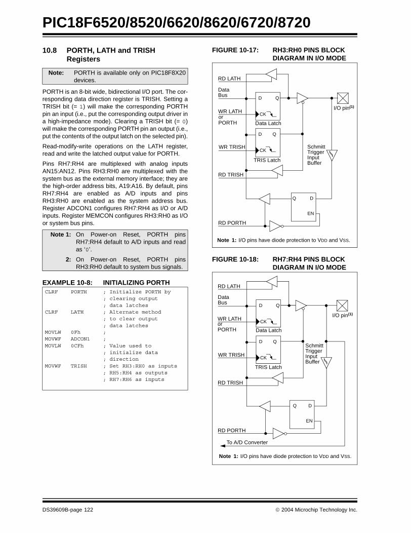
PIC18F6520/8520/6620/8620/6720/8720
10.8 PORTH, LATH and TRISH Registers
PORTH is an 8-bit wide, bidirectional I/O port. The cor-responding data direction register is TRISH. Setting aTRISH bit (= 1) will make the corresponding PORTHpin an input (i.e., put the corresponding output driver ina high-impedance mode). Clearing a TRISH bit (= 0)will make the corresponding PORTH pin an output (i.e.,put the contents of the output latch on the selected pin).
Read-modify-write operations on the LATH register,read and write the latched output value for PORTH.
Pins RH7:RH4 are multiplexed with analog inputsAN15:AN12. Pins RH3:RH0 are multiplexed with thesystem bus as the external memory interface; they arethe high-order address bits, A19:A16. By default, pinsRH7:RH4 are enabled as A/D inputs and pinsRH3:RH0 are enabled as the system address bus.Register ADCON1 configures RH7:RH4 as I/O or A/Dinputs. Register MEMCON configures RH3:RH0 as I/Oor system bus pins.
EXAMPLE 10-8: INITIALIZING PORTH
FIGURE 10-17: RH3:RH0 PINS BLOCK DIAGRAM IN I/O MODE
FIGURE 10-18: RH7:RH4 PINS BLOCK DIAGRAM IN I/O MODE
Note: PORTH is available only on PIC18F8X20devices.
Note 1: On Power-on Reset, PORTH pinsRH7:RH4 default to A/D inputs and readas ‘0’.
2: On Power-on Reset, PORTH pinsRH3:RH0 default to system bus signals.
CLRF PORTH ; Initialize PORTH by ; clearing output ; data latches CLRF LATH ; Alternate method ; to clear output ; data latches MOVLW 0Fh ; MOVWF ADCON1 ; MOVLW 0CFh ; Value used to ; initialize data ; direction MOVWF TRISH ; Set RH3:RH0 as inputs ; RH5:RH4 as outputs ; RH7:RH6 as inputs
DataBus
WR LATH
WR TRISH
RD PORTH
Data Latch
TRIS Latch
RD TRISH
SchmittTriggerInputBuffer
I/O pin(1)
QD
CK
QD
CK
EN
Q D
EN
RD LATH
orPORTH
Note 1: I/O pins have diode protection to VDD and VSS.
DataBus
WR LATH
WR TRISH
RD PORTH
Data Latch
TRIS Latch
RD TRISH
SchmittTriggerInputBuffer
I/O pin(1)
QD
CK
QD
CK
EN
Q D
EN
RD LATH
orPORTH
To A/D Converter
Note 1: I/O pins have diode protection to VDD and VSS.
DS39609B-page 122 2004 Microchip Technology Inc.

PIC18F6520/8520/6620/8620/6720/8720
FIGURE 10-19: RH3:RH0 PINS BLOCK DIAGRAM IN SYSTEM BUS MODE
To Instruction Register
External Enable
Address Out
Drive System
System BusControl
Data Bus
WR LATH
WR TRISH
RD PORTH
Data Latch
TRIS Latch
RD TRISH
TTLInputBuffer
I/O pin(1)
QD
CK
QD
CK
EN
Q D
EN
RD LATD
orPORTH
0
1
Port
Data
Instruction Read
Note 1: I/O pins have diode protection to VDD and VSS.
2004 Microchip Technology Inc. DS39609B-page 123

PIC18F6520/8520/6620/8620/6720/8720
TABLE 10-15: PORTH FUNCTIONS
TABLE 10-16: SUMMARY OF REGISTERS ASSOCIATED WITH PORTH
Name Bit# Buffer Type Function
RH0/A16 bit 0 ST/TTL(1) Input/output port pin or address bit 16 for external memory interface.
RH1/A17 bit 1 ST/TTL(1) Input/output port pin or address bit 17 for external memory interface.
RH2/A18 bit 2 ST/TTL(1) Input/output port pin or address bit 18 for external memory interface.
RH3/A19 bit 3 ST/TTL(1) Input/output port pin or address bit 19 for external memory interface.
RH4/AN12 bit 4 ST Input/output port pin or analog input channel 12.
RH5/AN13 bit 5 ST Input/output port pin or analog input channel 13.
RH6/AN14 bit 6 ST Input/output port pin or analog input channel 14.
RH7/AN15 bit 7 ST Input/output port pin or analog input channel 15.
Legend: ST = Schmitt Trigger input, TTL = TTL input Note 1: Input buffers are Schmitt Triggers when in I/O mode and TTL buffers when in System Bus or Parallel
Slave Port mode.
Name Bit 7 Bit 6 Bit 5 Bit 4 Bit 3 Bit 2 Bit 1 Bit 0Value on
POR, BOR
Value on all other Resets
TRISH PORTH Data Direction Control Register 1111 1111 1111 1111
PORTH Read PORTH pin/Write PORTH Data Latch xxxx xxxx uuuu uuuu
LATH Read PORTH Data Latch/Write PORTH Data Latch xxxx xxxx uuuu uuuu
ADCON1 — — VCFG1 VCFG0 PCFG3 PCFG2 PCFG1 PCFG0 --00 0000 --00 0000
MEMCON EBDIS — WAIT1 WAIT0 — — WM1 WM0 0-00 --00 0-00 --00
Legend: x = unknown, u = unchanged, – = unimplemented. Shaded cells are not used by PORTH.
DS39609B-page 124 2004 Microchip Technology Inc.

PIC18F6520/8520/6620/8620/6720/8720
10.9 PORTJ, TRISJ and LATJ Registers
PORTJ is an 8-bit wide, bidirectional port. The corre-sponding data direction register is TRISJ. Setting aTRISJ bit (= 1) will make the corresponding PORTJ pinan input (i.e., put the corresponding output driver in ahigh-impedance mode). Clearing a TRISJ bit (= 0) willmake the corresponding PORTJ pin an output (i.e., putthe contents of the output latch on the selected pin).
The Data Latch register (LATJ) is also memorymapped. Read-modify-write operations on the LATJregister, read and write the latched output value forPORTJ.
PORTJ is multiplexed with the system bus as the exter-nal memory interface; I/O port functions are only avail-able when the system bus is disabled. When operatingas the external memory interface, PORTJ provides thecontrol signal to external memory devices. The RJ5 pinis not multiplexed with any system bus functions.
When enabling peripheral functions, care should betaken in defining TRIS bits for each PORTJ pin. Someperipherals override the TRIS bit to make a pin anoutput, while other peripherals override the TRIS bit tomake a pin an input. The user should refer to the corre-sponding peripheral section for the correct TRIS bitsettings.
The pin override value is not loaded into the TRIS reg-ister. This allows read-modify-write of the TRIS register,without concern due to peripheral overrides.
EXAMPLE 10-9: INITIALIZING PORTJ
FIGURE 10-20: PORTJ BLOCK DIAGRAM IN I/O MODE
Note: PORTJ is available only on PIC18F8X20devices.
Note: On a Power-on Reset, these pins areconfigured as digital inputs.
CLRF PORTJ ; Initialize PORTG by; clearing output; data latches
CLRF LATJ ; Alternate method; to clear output; data latches
MOVLW 0xCF ; Value used to ; initialize data ; direction
MOVWF TRISJ ; Set RJ3:RJ0 as inputs; RJ5:RJ4 as output; RJ7:RJ6 as inputs
DataBus
WR LATJ
WR TRISJ
RD PORTJ
Data Latch
TRIS Latch
RD TRISJ
SchmittTriggerInputBuffer
I/O pin(1)
QD
CK
QD
CK
EN
Q D
EN
RD LATJ
orPORTJ
Note 1: I/O pins have diode protection to VDD and VSS.
2004 Microchip Technology Inc. DS39609B-page 125

PIC18F6520/8520/6620/8620/6720/8720
FIGURE 10-21: RJ4:RJ0 PINS BLOCK DIAGRAM IN SYSTEM BUS MODE
FIGURE 10-22: RJ7:RJ6 PINS BLOCK DIAGRAM IN SYSTEM BUS MODE
External Enable
Control Out
Drive System
System BusControl
Data Bus
WR LATJ
WR TRISJ
RD PORTJ
Data Latch
TRIS Latch
RD TRISJ
I/O pin(1)
QD
CK
QD
CK
EN
Q D
EN
RD LATJ
orPORTJ
0
1
Port
Data
Note 1: I/O pins have diode protection to VDD and VSS.
WM = 01
UB/LB Out
Drive SystemSystem Bus
Control
Data Bus
WR LATJ
WR TRISJ
RD PORTJ
Data Latch
TRIS Latch
RD TRISJ
I/O pin(1)
QD
CK
QD
CK
EN
Q D
EN
RD LATJ
orPORTJ
0
1
Port
Data
Note 1: I/O pins have diode protection to VDD and VSS.
DS39609B-page 126 2004 Microchip Technology Inc.

PIC18F6520/8520/6620/8620/6720/8720
TABLE 10-17: PORTJ FUNCTIONS
TABLE 10-18: SUMMARY OF REGISTERS ASSOCIATED WITH PORTJ
Name Bit# Buffer Type Function
RJ0/ALE bit 0 ST Input/output port pin or address latch enable control for external memory interface.
RJ1/OE bit 1 ST Input/output port pin or output enable control for external memory interface.
RJ2/WRL bit 2 ST Input/output port pin or write low byte control for external memory interface.
RJ3/WRH bit 3 ST Input/output port pin or write high byte control for external memory interface.
RJ4/BA0 bit 4 ST Input/output port pin or byte address 0 control for external memory interface.
RJ5/CE bit 5 ST Input/output port pin or chip enable control for external memory interface.
RJ6/LB bit 6 ST Input/output port pin or lower byte select control for external memory interface.
RJ7/UB bit 7 ST Input/output port pin or upper byte select control for external memory interface.
Legend: ST = Schmitt Trigger input
Name Bit 7 Bit 6 Bit 5 Bit 4 Bit 3 Bit 2 Bit 1 Bit 0Value on
POR, BOR
Value onall other Resets
PORTJ Read PORTJ pin/Write PORTJ Data Latch xxxx xxxx uuuu uuuu
LATJ LATJ Data Output Register xxxx xxxx uuuu uuuu
TRISJ Data Direction Control Register for PORTJ 1111 1111 1111 1111
Legend: x = unknown, u = unchanged
2004 Microchip Technology Inc. DS39609B-page 127

PIC18F6520/8520/6620/8620/6720/8720
10.10 Parallel Slave Port
PORTD also operates as an 8-bit wide Parallel SlavePort, or microprocessor port, when control bitPSPMODE (PSPCON<4>) is set. It is asynchronouslyreadable and writable by the external world through theRD control input pin, RE0/RD/AD8 and the WR controlinput pin, RE1/WR/AD9.
The PSP can directly interface to an 8-bit micro-processor data bus. The external microprocessor canread or write the PORTD latch as an 8-bit latch. Settingbit PSPMODE enables port pin RE0/RD/AD8 to be theRD input, RE1/WR/AD9 to be the WR input and RE2/CS/AD10 to be the CS (Chip Select) input. For thisfunctionality, the corresponding data direction bits ofthe TRISE register (TRISE<2:0>) must be configuredas inputs (set). The A/D port configuration bits,PCFG2:PCFG0 (ADCON1<2:0>), must be set whichwill configure pins RE2:RE0 as digital I/O.
A write to the PSP occurs when both the CS and WRlines are first detected low. A read from the PSP occurswhen both the CS and RD lines are first detected low.
The PORTE I/O pins become control inputs for themicroprocessor port when bit PSPMODE(PSPCON<4>) is set. In this mode, the user must makesure that the TRISE<2:0> bits are set (pins are config-ured as digital inputs) and the ADCON1 is configuredfor digital I/O. In this mode, the input buffers are TTL.
FIGURE 10-23: PORTD AND PORTE BLOCK DIAGRAM (PARALLEL SLAVE PORT)
Note: For PIC18F8X20 devices, the ParallelSlave Port is available only inMicrocontroller mode.
Data Bus
WR LATDRDx
QD
CK
EN
Q D
ENRD PORTD
pin
One bit of PORTD
Set Interrupt Flag
PSPIF (PIR1<7>)
Read
Chip Select
Write
RD
CS
WR
Note: I/O pin has protection diodes to VDD and VSS.
TTL
TTL
TTL
TTL
orPORTD
RD LATD
Data Latch
TRIS Latch
DS39609B-page 128 2004 Microchip Technology Inc.

PIC18F6520/8520/6620/8620/6720/8720
REGISTER 10-1: PSPCON REGISTER
FIGURE 10-24: PARALLEL SLAVE PORT WRITE WAVEFORMS
R-0 R-0 R/W-0 R/W-0 U-0 U-0 U-0 U-0
IBF OBF IBOV PSPMODE — — — —
bit 7 bit 0
bit 7 IBF: Input Buffer Full Status bit1 = A word has been received and is waiting to be read by the CPU0 = No word has been received
bit 6 OBF: Output Buffer Full Status bit
1 = The output buffer still holds a previously written word0 = The output buffer has been read
bit 5 IBOV: Input Buffer Overflow Detect bit1 = A write occurred when a previously input word has not been read
(must be cleared in software)0 = No overflow occurred
bit 4 PSPMODE: Parallel Slave Port Mode Select bit
1 = Parallel Slave Port mode0 = General Purpose I/O mode
bit 3-0 Unimplemented: Read as ‘0’
Legend:
R = Readable bit W = Writable bit U = Unimplemented bit, read as ‘0’
- n = Value at POR ‘1’ = Bit is set ‘0’ = Bit is cleared x = Bit is unknown
Q1 Q2 Q3 Q4
CS
Q1 Q2 Q3 Q4 Q1 Q2 Q3 Q4
WR
RD
IBF
OBF
PSPIF
PORTD<7:0>
2004 Microchip Technology Inc. DS39609B-page 129
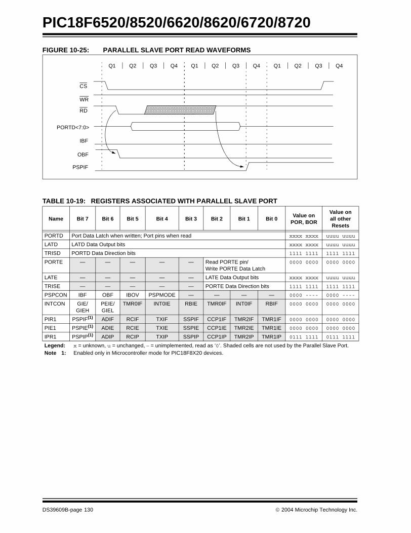
PIC18F6520/8520/6620/8620/6720/8720
FIGURE 10-25: PARALLEL SLAVE PORT READ WAVEFORMS
TABLE 10-19: REGISTERS ASSOCIATED WITH PARALLEL SLAVE PORT
Q1 Q2 Q3 Q4
CS
Q1 Q2 Q3 Q4 Q1 Q2 Q3 Q4
WR
IBF
PSPIF
RD
OBF
PORTD<7:0>
Name Bit 7 Bit 6 Bit 5 Bit 4 Bit 3 Bit 2 Bit 1 Bit 0Value on
POR, BOR
Value on all other Resets
PORTD Port Data Latch when written; Port pins when read xxxx xxxx uuuu uuuu
LATD LATD Data Output bits xxxx xxxx uuuu uuuu
TRISD PORTD Data Direction bits 1111 1111 1111 1111
PORTE — — — — — Read PORTE pin/Write PORTE Data Latch
0000 0000 0000 0000
LATE — — — — — LATE Data Output bits xxxx xxxx uuuu uuuu
TRISE — — — — — PORTE Data Direction bits 1111 1111 1111 1111
PSPCON IBF OBF IBOV PSPMODE — — — — 0000 ---- 0000 ----
INTCON GIE/GIEH
PEIE/GIEL
TMR0IF INT0IE RBIE TMR0IF INT0IF RBIF 0000 0000 0000 0000
PIR1 PSPIF(1) ADIF RCIF TXIF SSPIF CCP1IF TMR2IF TMR1IF 0000 0000 0000 0000
PIE1 PSPIE(1) ADIE RCIE TXIE SSPIE CCP1IE TMR2IE TMR1IE 0000 0000 0000 0000
IPR1 PSPIP(1) ADIP RCIP TXIP SSPIP CCP1IP TMR2IP TMR1IP 0111 1111 0111 1111
Legend: x = unknown, u = unchanged, – = unimplemented, read as ‘0’. Shaded cells are not used by the Parallel Slave Port.Note 1: Enabled only in Microcontroller mode for PIC18F8X20 devices.
DS39609B-page 130 2004 Microchip Technology Inc.

PIC18F6520/8520/6620/8620/6720/8720
11.0 TIMER0 MODULE
The Timer0 module has the following features:
• Software selectable as an 8-bit or 16-bit timer/counter
• Readable and writable• Dedicated 8-bit software programmable prescaler• Clock source selectable to be external or internal
• Interrupt-on-overflow from FFh to 00h in 8-bit mode and FFFFh to 0000h in 16-bit mode
• Edge select for external clock
Figure 11-1 shows a simplified block diagram of theTimer0 module in 8-bit mode and Figure 11-2 shows asimplified block diagram of the Timer0 module in 16-bitmode.
The T0CON register (Register 11-1) is a readable andwritable register that controls all the aspects of Timer0,including the prescale selection.
REGISTER 11-1: T0CON: TIMER0 CONTROL REGISTER R/W-1 R/W-1 R/W-1 R/W-1 R/W-1 R/W-1 R/W-1 R/W-1
TMR0ON T08BIT T0CS T0SE PSA T0PS2 T0PS1 T0PS0
bit 7 bit 0
bit 7 TMR0ON: Timer0 On/Off Control bit 1 = Enables Timer0 0 = Stops Timer0
bit 6 T08BIT: Timer0 8-bit/16-bit Control bit 1 = Timer0 is configured as an 8-bit timer/counter 0 = Timer0 is configured as a 16-bit timer/counter
bit 5 T0CS: Timer0 Clock Source Select bit
1 = Transition on T0CKI pin 0 = Internal instruction cycle clock (CLKO)
bit 4 T0SE: Timer0 Source Edge Select bit1 = Increment on high-to-low transition on T0CKI pin 0 = Increment on low-to-high transition on T0CKI pin
bit 3 PSA: Timer0 Prescaler Assignment bit 1 = TImer0 prescaler is NOT assigned. Timer0 clock input bypasses prescaler. 0 = Timer0 prescaler is assigned. Timer0 clock input comes from prescaler output.
bit 2-0 T0PS2:T0PS0: Timer0 Prescaler Select bits
111 = 1:256 prescale value110 = 1:128 prescale value101 = 1:64 prescale value100 = 1:32 prescale value011 = 1:16 prescale value010 = 1:8 prescale value001 = 1:4 prescale value000 = 1:2 prescale value
Legend:
R = Readable bit W = Writable bit U = Unimplemented bit, read as ‘0’
- n = Value at POR ‘1’ = Bit is set ‘0’ = Bit is cleared x = Bit is unknown
2004 Microchip Technology Inc. DS39609B-page 131
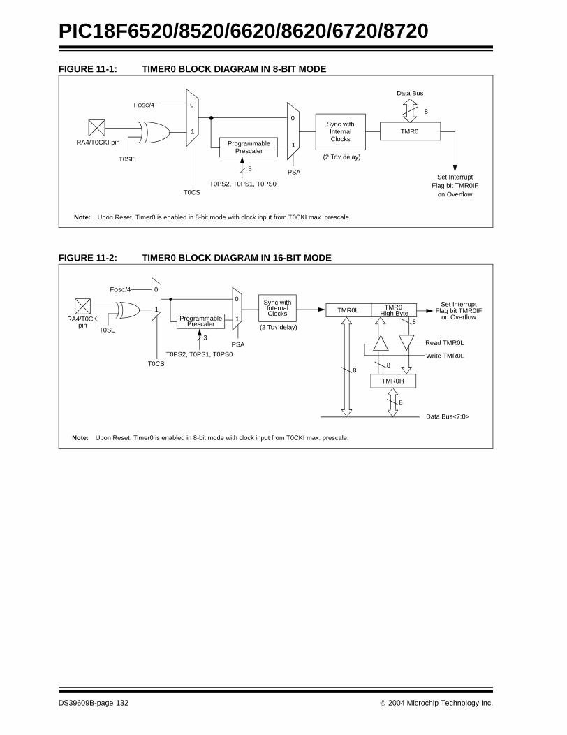
PIC18F6520/8520/6620/8620/6720/8720
FIGURE 11-1: TIMER0 BLOCK DIAGRAM IN 8-BIT MODE
FIGURE 11-2: TIMER0 BLOCK DIAGRAM IN 16-BIT MODE
Note: Upon Reset, Timer0 is enabled in 8-bit mode with clock input from T0CKI max. prescale.
RA4/T0CKI pin
T0SE
0
1
0
1
T0CS
FOSC/4
ProgrammablePrescaler
Sync withInternalClocks
TMR0
(2 TCY delay)
Data Bus
8
PSA
T0PS2, T0PS1, T0PS0Set Interrupt
Flag bit TMR0IFon Overflow
3
Note: Upon Reset, Timer0 is enabled in 8-bit mode with clock input from T0CKI max. prescale.
RA4/T0CKI
T0SE
0
1
0
1
T0CS
FOSC/4
ProgrammablePrescaler
Sync withInternalClocks TMR0L
(2 TCY delay)
Data Bus<7:0>
8
PSA
T0PS2, T0PS1, T0PS0
Set InterruptFlag bit TMR0IF
on Overflow
3
TMR0
TMR0H
High Byte
88
8
Read TMR0L
Write TMR0L
pin
DS39609B-page 132 2004 Microchip Technology Inc.

PIC18F6520/8520/6620/8620/6720/8720
11.1 Timer0 Operation
Timer0 can operate as a timer or as a counter.
Timer mode is selected by clearing the T0CS bit. InTimer mode, the Timer0 module will increment everyinstruction cycle (without prescaler). If the TMR0 regis-ter is written, the increment is inhibited for the followingtwo instruction cycles. The user can work around thisby writing an adjusted value to the TMR0 register.
Counter mode is selected by setting the T0CS bit. InCounter mode, Timer0 will increment, either on everyrising or falling edge of pin RA4/T0CKI. The increment-ing edge is determined by the Timer0 Source EdgeSelect bit (T0SE). Clearing the T0SE bit selects therising edge. Restrictions on the external clock input arediscussed below.
When an external clock input is used for Timer0, it mustmeet certain requirements. The requirements ensurethe external clock can be synchronized with the internalphase clock (TOSC). Also, there is a delay in the actualincrementing of Timer0 after synchronization.
11.2 Prescaler
An 8-bit counter is available as a prescaler for the Timer0module. The prescaler is not readable or writable.
The PSA and T0PS2:T0PS0 bits determine theprescaler assignment and prescale ratio.
Clearing bit PSA will assign the prescaler to the Timer0module. When the prescaler is assigned to the Timer0module, prescale values of 1:2, 1:4, ..., 1:256 areselectable.
When assigned to the Timer0 module, all instructionswriting to the TMR0 register (e.g., CLRF TMR0, MOVWFTMR0, BSF TMR0, x, ..., etc.) will clear the prescalercount.
11.2.1 SWITCHING PRESCALER ASSIGNMENT
The prescaler assignment is fully under softwarecontrol, (i.e., it can be changed “on-the-fly” duringprogram execution).
11.3 Timer0 Interrupt
The TMR0 interrupt is generated when the TMR0register overflows from FFh to 00h in 8-bit mode, orFFFFh to 0000h in 16-bit mode. This overflow sets theTMR0IF bit. The interrupt can be masked by clearingthe TMR0IE bit. The TMR0IF bit must be cleared insoftware by the Timer0 module Interrupt ServiceRoutine before re-enabling this interrupt. The TMR0interrupt cannot awaken the processor from Sleep,since the timer is shut-off during Sleep.
11.4 16-Bit Mode Timer Reads and Writes
TMR0H is not the high byte of the timer/counter in16-bit mode, but is actually a buffered version of thehigh byte of Timer0 (refer to Figure 11-2). The high byteof the Timer0 counter/timer is not directly readable norwritable. TMR0H is updated with the contents of thehigh byte of Timer0 during a read of TMR0L. This pro-vides the ability to read all 16 bits of Timer0 withouthaving to verify that the read of the high and low bytewere valid, due to a rollover between successive readsof the high and low byte.
A write to the high byte of Timer0 must also take placethrough the TMR0H Buffer register. Timer0 high byte isupdated with the contents of TMR0H when a writeoccurs to TMR0L. This allows all 16 bits of Timer0 to beupdated at once.
TABLE 11-1: REGISTERS ASSOCIATED WITH TIMER0
Note: Writing to TMR0 when the prescaler isassigned to Timer0, will clear theprescaler count, but will not change theprescaler assignment.
Name Bit 7 Bit 6 Bit 5 Bit 4 Bit 3 Bit 2 Bit 1 Bit 0Value on
POR, BOR
Value on all other Resets
TMR0L Timer0 Module Low Byte Register xxxx xxxx uuuu uuuu
TMR0H Timer0 Module High Byte Register 0000 0000 0000 0000
INTCON GIE/GIEH PEIE/GIEL TMR0IE INT0IE RBIE TMR0IF INT0IF RBIF 0000 0000 0000 0000
T0CON TMR0ON T08BIT T0CS T0SE PSA T0PS2 T0PS1 T0PS0 1111 1111 1111 1111
TRISA — PORTA Data Direction Register -111 1111 -111 1111
Legend: x = unknown, u = unchanged, – = unimplemented locations, read as ‘0’. Shaded cells are not used by Timer0.
2004 Microchip Technology Inc. DS39609B-page 133

PIC18F6520/8520/6620/8620/6720/8720
NOTES:
DS39609B-page 134 2004 Microchip Technology Inc.

PIC18F6520/8520/6620/8620/6720/8720
12.0 TIMER1 MODULE
The Timer1 module timer/counter has the followingfeatures:
• 16-bit timer/counter(two 8-bit registers: TMR1H and TMR1L)
• Readable and writable (both registers)
• Internal or external clock select• Interrupt-on-overflow from FFFFh to 0000h• Reset from CCP module special event trigger
Figure 12-1 is a simplified block diagram of the Timer1module.
Register 12-1 details the Timer1 Control register. Thisregister controls the operating mode of the Timer1module and contains the Timer1 Oscillator Enable bit(T1OSCEN). Timer1 can be enabled or disabled bysetting or clearing control bit, TMR1ON (T1CON<0>).
Timer1 can also be used to provide Real-Time Clock(RTC) functionality to applications, with only a minimaladdition of external components and code overhead.
REGISTER 12-1: T1CON: TIMER1 CONTROL REGISTER R/W-0 U-0 R/W-0 R/W-0 R/W-0 R/W-0 R/W-0 R/W-0
RD16 — T1CKPS1 T1CKPS0 T1OSCEN T1SYNC TMR1CS TMR1ON
bit 7 bit 0
bit 7 RD16: 16-bit Read/Write Mode Enable bit1 = Enables register read/write of Timer1 in one 16-bit operation0 = Enables register read/write of Timer1 in two 8-bit operations
bit 6 Unimplemented: Read as ‘0’
bit 5-4 T1CKPS1:T1CKPS0: Timer1 Input Clock Prescale Select bits11 = 1:8 Prescale value 10 = 1:4 Prescale value 01 = 1:2 Prescale value 00 = 1:1 Prescale value
bit 3 T1OSCEN: Timer1 Oscillator Enable bit1 = Timer1 oscillator is enabled 0 = Timer1 oscillator is shut offThe oscillator inverter and feedback resistor are turned off to eliminate power drain.
bit 2 T1SYNC: Timer1 External Clock Input Synchronization Select bit
When TMR1CS = 1: 1 = Do not synchronize external clock input 0 = Synchronize external clock inputWhen TMR1CS = 0: This bit is ignored. Timer1 uses the internal clock when TMR1CS = 0.
bit 1 TMR1CS: Timer1 Clock Source Select bit1 = External clock from pin RC0/T1OSO/T13CKI (on the rising edge) 0 = Internal clock (FOSC/4)
bit 0 TMR1ON: Timer1 On bit
1 = Enables Timer1 0 = Stops Timer1
Legend:
R = Readable bit W = Writable bit U = Unimplemented bit, read as ‘0’
- n = Value at POR ‘1’ = Bit is set ‘0’ = Bit is cleared x = Bit is unknown
2004 Microchip Technology Inc. DS39609B-page 135

PIC18F6520/8520/6620/8620/6720/8720
12.1 Timer1 Operation
Timer1 can operate in one of these modes:
• As a timer
• As a synchronous counter• As an asynchronous counter
The operating mode is determined by the clock selectbit, TMR1CS (T1CON<1>).
When TMR1CS = 0, Timer1 increments every instruc-tion cycle. When TMR1CS = 1, Timer1 increments onevery rising edge of the external clock input or theTimer1 oscillator, if enabled.
When the Timer1 oscillator is enabled (T1OSCEN isset), the RC1/T1OSI and RC0/T1OSO/T13CKI pinsbecome inputs. That is, the TRISC<1:0> value isignored and the pins are read as ‘0’.
Timer1 also has an internal “Reset input”. ThisReset can be generated by the CCP module(see Section 16.0 “Capture/Compare/PWM (CCP)Modules”).
FIGURE 12-1: TIMER1 BLOCK DIAGRAM
FIGURE 12-2: TIMER1 BLOCK DIAGRAM: 16-BIT READ/WRITE MODE
TMR1H TMR1L
T1SYNC
TMR1CS
T1CKPS1:T1CKPS0Sleep Input
FOSC/4InternalClock
TMR1ONOn/Off
Prescaler1, 2, 4, 8
Synchronize
det
1
0
0
1
SynchronizedClock Input
2
TMR1IFOverflow
TMR1CLR
CCP Special Event Trigger
T1OSCENEnableOscillator(1)
T1OSC
InterruptFlag Bit
Note 1: When enable bit T1OSCEN is cleared, the inverter and feedback resistor are turned off. This eliminates power drain.
T1OSI
T1OSO/T13CKI
Timer 1 TMR1L
T1OSCT1SYNC
TMR1CS
T1CKPS1:T1CKPS0
Sleep Input
T1OSCENEnableOscillator(1)
TMR1IFOverflowInterrupt
FOSC/4InternalClock
TMR1ONOn/Off
Prescaler1, 2, 4, 8
Synchronize
det
1
0
0
1
SynchronizedClock Input
2
T1OSO/T13CKI
T1OSI
TMR1
Flag bit
Note 1: When enable bit T1OSCEN is cleared, the inverter and feedback resistor are turned off. This eliminates power drain.
High Byte
Data Bus<7:0>
8
TMR1H
88
8
Read TMR1L
Write TMR1L
CLR
CCP Special Event Trigger
DS39609B-page 136 2004 Microchip Technology Inc.

PIC18F6520/8520/6620/8620/6720/8720
12.2 Timer1 Oscillator
A crystal oscillator circuit is built-in between pins T1OSI(input) and T1OSO (amplifier output). It is enabled bysetting control bit, T1OSCEN (T1CON<3>). The oscil-lator is a low-power oscillator, rated up to 200 kHz. Itwill continue to run during Sleep. It is primarily intendedfor a 32 kHz crystal. The circuit for a typical LP oscilla-tor is shown in Figure 12-3. Table 12-1 shows thecapacitor selection for the Timer1 oscillator.
The user must provide a software time delay to ensureproper start-up of the Timer1 oscillator
FIGURE 12-3: EXTERNAL COMPONENTS FOR THE TIMER1 LP OSCILLATOR
12.2.1 LOW-POWER TIMER1 OPTION (PIC18FX520 DEVICES ONLY)
The Timer1 oscillator for PIC18LFX520 devices incor-porates a low-power feature, which allows the oscillatorto automatically reduce its power consumption whenthe microcontroller is in Sleep mode.
As high noise environments may cause excessiveoscillator instability in Sleep mode, this option is bestsuited for low noise applications where powerconservation is an important design consideration. Dueto the low-power nature of the oscillator, it may also besensitive to rapidly changing signals in close proximity.
The oscillator circuit, shown in Figure 12-3, should belocated as close as possible to the microcontroller.There should be no circuits passing within the oscillatorcircuit boundaries other than VSS or VDD.
If a high-speed circuit must be located near the oscilla-tor (such as the CCP1 pin in output compare or PWMmode, or the primary oscillator using the OSC2 pin), agrounded guard ring around the oscillator circuit, asshown in Figure 12-4, may be helpful when used on asingle-sided PCB or in addition to a ground plane.
FIGURE 12-4: OSCILLATOR CIRCUIT WITH GROUNDED GUARD RING
TABLE 12-1: CAPACITOR SELECTION FOR THE ALTERNATE OSCILLATOR
Osc Type Freq C1 C2
LP 32 kHz TBD(1) TBD(1)
Crystal to be Tested:
32.768 kHz Epson C-001R32.768K-A ± 20 PPM
Note 1: Microchip suggests 33 pF as a startingpoint in validating the oscillator circuit.
2: Higher capacitance increases the stabilityof the oscillator, but also increases thestart-up time.
3: Since each resonator/crystal has its owncharacteristics, the user should consultthe resonator/crystal manufacturer forappropriate values of externalcomponents.
4: Capacitor values are for design guidanceonly.
Note: See the Notes with Table 12-1 for additionalinformation about capacitor selection.
C1
C2
XTAL
PIC18FXX20
T1OSI
T1OSO
32.768 kHz
33 pF
33 pF
Note: PIC18FX620/X720 devices have thestandard Timer1 oscillator permanentlyselected. PIC18LFX620/X720 deviceshave the low-power Timer1 oscillatorpermanently selected.
VDD
OSC1
VSS
OSC2
RC0
RC1
RC2
Note: Not drawn to scale.
2004 Microchip Technology Inc. DS39609B-page 137

PIC18F6520/8520/6620/8620/6720/8720
12.3 Timer1 Interrupt
The TMR1 register pair (TMR1H:TMR1L) incrementsfrom 0000h to FFFFh and rolls over to 0000h. TheTMR1 interrupt, if enabled, is generated on overflow,which is latched in interrupt flag bit, TMR1IF(PIR1<0>). This interrupt can be enabled/disabled bysetting/clearing TMR1 Interrupt Enable bit, TMR1IE(PIE1<0>).
12.4 Resetting Timer1 Using a CCP Trigger Output
If the CCP module is configured in Compare modeto generate a “special event trigger”(CCP1M3:CCP1M0 = 1011), this signal will resetTimer1 and start an A/D conversion (if the A/D moduleis enabled).
Timer1 must be configured for either Timer or Synchro-nized Counter mode to take advantage of this feature.If Timer1 is running in Asynchronous Counter mode,this Reset operation may not work.
In the event that a write to Timer1 coincides with aspecial event trigger from CCP1, the write will takeprecedence.
In this mode of operation, the CCPR1H:CCPR1Lregister pair effectively becomes the period register forTimer1.
12.5 Timer1 16-Bit Read/Write Mode
Timer1 can be configured for 16-bit reads and writes(see Figure 12-2). When the RD16 control bit(T1CON<7>) is set, the address for TMR1H is mappedto a buffer register for the high byte of Timer1. A readfrom TMR1L will load the contents of the high byte ofTimer1 into the Timer1 high byte buffer. This providesthe user with the ability to accurately read all 16 bits ofTimer1 without having to determine whether a read ofthe high byte, followed by a read of the low byte, isvalid, due to a rollover between reads.
A write to the high byte of Timer1 must also take placethrough the TMR1H Buffer register. Timer1 high byte isupdated with the contents of TMR1H when a writeoccurs to TMR1L. This allows a user to write all 16 bitsto both the high and low bytes of Timer1 at once.
The high byte of Timer1 is not directly readable or writ-able in this mode. All reads and writes must take placethrough the Timer1 High Byte Buffer register. Writes toTMR1H do not clear the Timer1 prescaler. Theprescaler is only cleared on writes to TMR1L.
12.6 Using Timer1 as a Real-Time Clock
Adding an external LP oscillator to Timer1 (such as theone described in Section 12.2 “Timer1 Oscillator”)gives users the option to include RTC functionality totheir applications. This is accomplished with an inex-pensive watch crystal to provide an accurate time baseand several lines of application code to calculate thetime. When operating in Sleep mode and using abattery or supercapacitor as a power source, it cancompletely eliminate the need for a separate RTCdevice and battery backup.
The application code routine, RTCisr, shown inExample 12-1, demonstrates a simple method to incre-ment a counter at one-second intervals using anInterrupt Service Routine. Incrementing the TMR1register pair to overflow, triggers the interrupt and callsthe routine, which increments the seconds counter byone; additional counters for minutes and hours areincremented as the previous counter overflow.
Since the register pair is 16 bits wide, counting up tooverflow the register directly from a 32.768 kHz clockwould take 2 seconds. To force the overflow at therequired one-second intervals, it is necessary topreload it; the simplest method is to set the MSb ofTMR1H with a BSF instruction. Note that the TMR1Lregister is never preloaded or altered; doing so mayintroduce cumulative error over many cycles.
For this method to be accurate, Timer1 must operate inAsynchronous mode and the Timer1 overflow interruptmust be enabled (PIE1<0> = 1), as shown in theroutine, RTCinit. The Timer1 oscillator must also beenabled and running at all times.
Note: The special event triggers from the CCP1module will not set interrupt flag bitTMR1IF (PIR1<0>).
DS39609B-page 138 2004 Microchip Technology Inc.

PIC18F6520/8520/6620/8620/6720/8720
EXAMPLE 12-1: IMPLEMENTING A REAL-TIME CLOCK USING A TIMER1 INTERRUPT SERVICE
TABLE 12-2: REGISTERS ASSOCIATED WITH TIMER1 AS A TIMER/COUNTER
RTCinitMOVLW 0x80 ; Preload TMR1 register pairMOVWF TMR1H ; for 1 second overflowCLRF TMR1LMOVLW b’00001111’ ; Configure for external clock,MOVWF T1OSC ; Asynchronous operation, external oscillatorCLRF secs ; Initialize timekeeping registersCLRF mins ; MOVLW .12MOVWF hoursBSF PIE1, TMR1IE ; Enable Timer1 interruptRETURN
RTCisrBSF TMR1H, 7 ; Preload for 1 sec overflowBCF PIR1, TMR1IF ; Clear interrupt flagINCF secs, F ; Increment secondsMOVLW .59 ; 60 seconds elapsed?CPFSGT secsRETURN ; No, doneCLRF secs ; Clear secondsINCF mins, F ; Increment minutesMOVLW .59 ; 60 minutes elapsed?CPFSGT minsRETURN ; No, doneCLRF mins ; clear minutesINCF hours, F ; Increment hoursMOVLW .23 ; 24 hours elapsed?CPFSGT hoursRETURN ; No, doneMOVLW .01 ; Reset hours to 1MOVWF hoursRETURN ; Done
Name Bit 7 Bit 6 Bit 5 Bit 4 Bit 3 Bit 2 Bit 1 Bit 0Value on
POR, BOR
Value on all other Resets
INTCON GIE/GIEH PEIE/GIEL TMR0IE INT0IE RBIE TMR0IF INT0IF RBIF 0000 0000 0000 0000
PIR1 PSPIF ADIF RCIF TXIF SSPIF CCP1IF TMR2IF TMR1IF 0000 0000 0000 0000
PIE1 PSPIE ADIE RCIE TXIE SSPIE CCP1IE TMR2IE TMR1IE 0000 0000 0000 0000
IPR1 PSPIP ADIP RCIP TXIP SSPIP CCP1IP TMR2IP TMR1IP 0111 1111 0111 1111
TMR1L Holding Register for the Least Significant Byte of the 16-bit TMR1 Register xxxx xxxx uuuu uuuu
TMR1H Holding Register for the Most Significant Byte of the 16-bit TMR1 Register xxxx xxxx uuuu uuuu
T1CON RD16 — T1CKPS1 T1CKPS0 T1OSCEN T1SYNC TMR1CS TMR1ON 0-00 0000 u-uu uuuu
Legend: x = unknown, u = unchanged, – = unimplemented, read as ‘0’. Shaded cells are not used by the Timer1 module.
2004 Microchip Technology Inc. DS39609B-page 139

PIC18F6520/8520/6620/8620/6720/8720
NOTES:
DS39609B-page 140 2004 Microchip Technology Inc.

PIC18F6520/8520/6620/8620/6720/8720
13.0 TIMER2 MODULE
The Timer2 module timer has the following features:
• 8-bit timer (TMR2 register)• 8-bit period register (PR2)• Readable and writable (both registers)
• Software programmable prescaler (1:1, 1:4, 1:16)• Software programmable postscaler (1:1 to 1:16)• Interrupt on TMR2 match of PR2
• SSP module optional use of TMR2 output to generate clock shift
Timer2 has a control register shown in Register 13-1.Timer2 can be shut-off by clearing control bit, TMR2ON(T2CON<2>), to minimize power consumption.Figure 13-1 is a simplified block diagram of the Timer2module. Register 13-1 shows the Timer2 Control regis-ter. The prescaler and postscaler selection of Timer2are controlled by this register.
13.1 Timer2 Operation
Timer2 can be used as the PWM time base for thePWM mode of the CCP module. The TMR2 register isreadable and writable and is cleared on any deviceReset. The input clock (FOSC/4) has a prescale optionof 1:1, 1:4 or 1:16, selected by control bits,T2CKPS1:T2CKPS0 (T2CON<1:0>). The match out-put of TMR2 goes through a 4-bit postscaler (whichgives a 1:1 to 1:16 scaling inclusive) to generate aTMR2 interrupt (latched in flag bit, TMR2IF (PIR1<1>)).
The prescaler and postscaler counters are clearedwhen any of the following occurs:
• a write to the TMR2 register
• a write to the T2CON register• any device Reset (Power-on Reset, MCLR Reset,
Watchdog Timer Reset or Brown-out Reset)
TMR2 is not cleared when T2CON is written.
REGISTER 13-1: T2CON: TIMER2 CONTROL REGISTER U-0 R/W-0 R/W-0 R/W-0 R/W-0 R/W-0 R/W-0 R/W-0
— T2OUTPS3 T2OUTPS2 T2OUTPS1 T2OUTPS0 TMR2ON T2CKPS1 T2CKPS0
bit 7 bit 0
bit 7 Unimplemented: Read as ‘0’
bit 6-3 T2OUTPS3:T2OUTPS0: Timer2 Output Postscale Select bits0000 = 1:1 Postscale 0001 = 1:2 Postscale • • • 1111 = 1:16 Postscale
bit 2 TMR2ON: Timer2 On bit1 = Timer2 is on 0 = Timer2 is off
bit 1-0 T2CKPS1:T2CKPS0: Timer2 Clock Prescale Select bits00 = Prescaler is 1 01 = Prescaler is 4 1x = Prescaler is 16
Legend:
R = Readable bit W = Writable bit U = Unimplemented bit, read as ‘0’
- n = Value at POR ‘1’ = Bit is set ‘0’ = Bit is cleared x = Bit is unknown
2004 Microchip Technology Inc. DS39609B-page 141

PIC18F6520/8520/6620/8620/6720/8720
13.2 Timer2 Interrupt
The Timer2 module has an 8-bit period register, PR2.Timer2 increments from 00h until it matches PR2 andthen resets to 00h on the next increment cycle. PR2 isa readable and writable register. The PR2 register isinitialized to FFh upon Reset.
13.3 Output of TMR2
The output of TMR2 (before the postscaler) is fed to thesynchronous serial port module, which optionally usesit to generate the shift clock.
FIGURE 13-1: TIMER2 BLOCK DIAGRAM
TABLE 13-1: REGISTERS ASSOCIATED WITH TIMER2 AS A TIMER/COUNTER
Name Bit 7 Bit 6 Bit 5 Bit 4 Bit 3 Bit 2 Bit 1 Bit 0Value on
POR, BOR
Value on all other Resets
INTCON GIE/GIEH PEIE/GIEL TMR0IE INT0IE RBIE TMR0IF INT0IF RBIF 0000 0000 0000 0000
PIR1 PSPIF ADIF RCIF TXIF SSPIF CCP1IF TMR2IF TMR1IF 0000 0000 0000 0000
PIE1 PSPIE ADIE RCIE TXIE SSPIE CCP1IE TMR2IE TMR1IE 0000 0000 0000 0000
IPR1 PSPIP ADIP RCIP TXIP SSPIP CCP1IP TMR2IP TMR1IP 0111 1111 0111 1111
TMR2 Timer2 Module Register 0000 0000 0000 0000
T2CON — T2OUTPS3 T2OUTPS2 T2OUTPS1 T2OUTPS0 TMR2ON T2CKPS1 T2CKPS0 -000 0000 -000 0000
PR2 Timer2 Period Register 1111 1111 1111 1111
Legend: x = unknown, u = unchanged, – = unimplemented, read as ‘0’. Shaded cells are not used by the Timer2 module.
Comparator
TMR2Sets Flag
TMR2
Output(1)
Reset
Postscaler
Prescaler
PR2
2
FOSC/4
1:1 to 1:16
1:1, 1:4, 1:16
EQ
4
bit TMR2IF
Note 1: TMR2 register output can be software selected by the SSP module as a baud clock.
T2OUTPS3:T2OUTPS0
T2CKPS1:T2CKPS0
DS39609B-page 142 2004 Microchip Technology Inc.

PIC18F6520/8520/6620/8620/6720/8720
14.0 TIMER3 MODULE
The Timer3 module timer/counter has the followingfeatures:
• 16-bit timer/counter(two 8-bit registers; TMR3H and TMR3L)
• Readable and writable (both registers)
• Internal or external clock select• Interrupt-on-overflow from FFFFh to 0000h• Reset from CCP module trigger
Figure 14-1 is a simplified block diagram of the Timer3module.
Register 14-1 shows the Timer3 Control register. Thisregister controls the operating mode of the Timer3module and sets the CCP clock source.
Register 12-1 shows the Timer1 Control register. Thisregister controls the operating mode of the Timer1module, as well as contains the Timer1 OscillatorEnable bit (T1OSCEN), which can be a clock source forTimer3.
REGISTER 14-1: T3CON: TIMER3 CONTROL REGISTER R/W-0 R/W-0 R/W-0 R/W-0 R/W-0 R/W-0 R/W-0 R/W-0
RD16 T3CCP2 T3CKPS1 T3CKPS0 T3CCP1 T3SYNC TMR3CS TMR3ON
bit 7 bit 0
bit 7 RD16: 16-bit Read/Write Mode Enable bit1 = Enables register read/write of Timer3 in one 16-bit operation0 = Enables register read/write of Timer3 in two 8-bit operations
bit 6, 3 T3CCP2:T3CCP1: Timer3 and Timer1 to CCPx Enable bits11 = Timer3 and Timer4 are the clock sources for CCP1 through CCP510 = Timer3 and Timer4 are the clock sources for CCP3 through CCP5;
Timer1 and Timer2 are the clock sources for CCP1 and CCP201 = Timer3 and Timer4 are the clock sources for CCP2 through CCP5;
Timer1 and Timer2 are the clock sources for CCP100 = Timer1 and Timer2 are the clock sources for CCP1 through CCP5
bit 5-4 T3CKPS1:T3CKPS0: Timer3 Input Clock Prescale Select bits11 = 1:8 Prescale value10 = 1:4 Prescale value01 = 1:2 Prescale value00 = 1:1 Prescale value
bit 2 T3SYNC: Timer3 External Clock Input Synchronization Control bit (Not usable if the system clock comes from Timer1/Timer3.)When TMR3CS = 1:1 = Do not synchronize external clock input0 = Synchronize external clock input
When TMR3CS = 0:This bit is ignored. Timer3 uses the internal clock when TMR3CS = 0.
bit 1 TMR3CS: Timer3 Clock Source Select bit1 = External clock input from Timer1 oscillator or T13CKI (on the rising edge after the
first falling edge)0 = Internal clock (FOSC/4)
bit 0 TMR3ON: Timer3 On bit
1 = Enables Timer3 0 = Stops Timer3
Legend:
R = Readable bit W = Writable bit U = Unimplemented bit, read as ‘0’
- n = Value at POR ‘1’ = Bit is set ‘0’ = Bit is cleared x = Bit is unknown
2004 Microchip Technology Inc. DS39609B-page 143

PIC18F6520/8520/6620/8620/6720/8720
14.1 Timer3 Operation
Timer3 can operate in one of these modes:
• As a timer
• As a synchronous counter• As an asynchronous counter
The operating mode is determined by the clock selectbit, TMR3CS (T3CON<1>).
When TMR3CS = 0, Timer3 increments every instruc-tion cycle. When TMR3CS = 1, Timer3 increments onevery rising edge of the Timer1 external clock input orthe Timer1 oscillator, if enabled.
When the Timer1 oscillator is enabled (T1OSCEN isset), the RC1/T1OSI and RC0/T1OSO/T13CKI pinsbecome inputs. That is, the TRISC<1:0> value isignored and the pins are read as ‘0’.
Timer3 also has an internal “Reset input”. This Resetcan be generated by the CCP module (see Section 14.0“Timer3 Module”).
FIGURE 14-1: TIMER3 BLOCK DIAGRAM
FIGURE 14-2: TIMER3 BLOCK DIAGRAM CONFIGURED IN 16-BIT READ/WRITE MODE
TMR3H TMR3L
T1OSC
T3SYNC
TMR3CS
T3CKPS1:T3CKPS0
Sleep Input
T1OSCENEnableOscillator(1)
TMR3IFOverflowInterrupt
FOSC/4InternalClock
TMR3ONOn/Off
Prescaler1, 2, 4, 8
Synchronize
det
1
0
0
1
SynchronizedClock Input
2
T1OSO/
T1OSI
Flag bit
(3)
Note 1: When enable bit T1OSCEN is cleared, the inverter and feedback resistor are turned off. This eliminates power drain.
T13CKI
CLR
CCP Special TriggerT3CCPx
Timer3TMR3L
T1OSCT3SYNC
TMR3CST3CKPS1:T3CKPS0
Sleep Input
T1OSCENEnableOscillator(1)
FOSC/4InternalClock
TMR3ONOn/Off
Prescaler1, 2, 4, 8
Synchronize
det
1
0
0
1
SynchronizedClock Input
2
T1OSO/
T1OSI
TMR3
T13CKI
CLR
CCP Special TriggerT3CCPx
To Timer1 Clock Input
Note 1: When the T1OSCEN bit is cleared, the inverter and feedback resistor are turned off. This eliminates power drain.
High Byte
Data Bus<7:0>
8
TMR3H
88
8
Read TMR3L
Write TMR3L
Set TMR3IF Flag biton Overflow
DS39609B-page 144 2004 Microchip Technology Inc.

PIC18F6520/8520/6620/8620/6720/8720
14.2 Timer1 Oscillator
The Timer1 oscillator may be used as the clock sourcefor Timer3. The Timer1 oscillator is enabled by settingthe T1OSCEN (T1CON<3>) bit. The oscillator is a low-power oscillator rated up to 200 kHz. See Section 12.0“Timer1 Module” for further details.
14.3 Timer3 Interrupt
The TMR3 register pair (TMR3H:TMR3L) incrementsfrom 0000h to FFFFh and rolls over to 0000h. TheTMR3 interrupt, if enabled, is generated on overflow,which is latched in interrupt flag bit, TMR3IF(PIR2<1>). This interrupt can be enabled/disabled bysetting/clearing TMR3 Interrupt Enable bit, TMR3IE(PIE2<1>).
14.4 Resetting Timer3 Using a CCP Trigger Output
If the CCP module is configured in Compare modeto generate a “special event trigger”(CCP1M3:CCP1M0 = 1011), this signal will resetTimer3.
Timer3 must be configured for either Timer or Synchro-nized Counter mode to take advantage of this feature.If Timer3 is running in Asynchronous Counter mode,this Reset operation may not work. In the event that awrite to Timer3 coincides with a special event triggerfrom CCP1, the write will take precedence. In this modeof operation, the CCPR1H:CCPR1L register paireffectively becomes the period register for Timer3.
TABLE 14-1: REGISTERS ASSOCIATED WITH TIMER3 AS A TIMER/COUNTER
Note: The special event triggers from the CCPmodule will not set interrupt flag bit,TMR3IF (PIR1<0>).
Name Bit 7 Bit 6 Bit 5 Bit 4 Bit 3 Bit 2 Bit 1 Bit 0Value on
POR, BOR
Value onall other Resets
INTCON GIE/GIEH PEIE/GIEL TMR0IE INT0IE RBIE TMR0IF INT0IF RBIF 0000 0000 0000 0000
PIR2 — — — EEIF BCLIF LVDIF TMR3IF CCP2IF ---0 0000 ---0 0000
PIE2 — — — EEIE BCLIE LVDIE TMR3IE CCP2IE ---0 0000 ---0 0000
IPR2 — — — EEIP BCLIP LVDIP TMR3IP CCP2IP ---1 1111 ---1 1111
TMR3L Holding Register for the Least Significant Byte of the 16-bit TMR3 Register xxxx xxxx uuuu uuuu
TMR3H Holding Register for the Most Significant Byte of the 16-bit TMR3 Register xxxx xxxx uuuu uuuu
T1CON RD16 — T1CKPS1 T1CKPS0 T1OSCEN T1SYNC TMR1CS TMR1ON 0-00 0000 u-uu uuuu
T3CON RD16 T3CCP2 T3CKPS1 T3CKPS0 T3CCP1 T3SYNC TMR3CS TMR3ON 0000 0000 uuuu uuuu
Legend: x = unknown, u = unchanged, – = unimplemented, read as ‘0’. Shaded cells are not used by the Timer3 module.
2004 Microchip Technology Inc. DS39609B-page 145

PIC18F6520/8520/6620/8620/6720/8720
NOTES:
DS39609B-page 146 2004 Microchip Technology Inc.

PIC18F6520/8520/6620/8620/6720/8720
15.0 TIMER4 MODULE
The Timer4 module timer has the following features:
• 8-bit timer (TMR4 register)• 8-bit period register (PR4)• Readable and writable (both registers)
• Software programmable prescaler (1:1, 1:4, 1:16)• Software programmable postscaler (1:1 to 1:16)• Interrupt on TMR4 match of PR4
Timer4 has a control register shown in Register 15-1.Timer4 can be shut-off by clearing control bit, TMR4ON(T4CON<2>), to minimize power consumption. Theprescaler and postscaler selection of Timer4 are alsocontrolled by this register. Figure 15-1 is a simplifiedblock diagram of the Timer4 module.
15.1 Timer4 Operation
Timer4 can be used as the PWM time base for thePWM mode of the CCP module. The TMR4 register isreadable and writable and is cleared on any deviceReset. The input clock (FOSC/4) has a prescale optionof 1:1, 1:4 or 1:16, selected by control bitsT4CKPS1:T4CKPS0 (T4CON<1:0>). The match out-put of TMR4 goes through a 4-bit postscaler (whichgives a 1:1 to 1:16 scaling inclusive) to generate aTMR4 interrupt, latched in flag bit, TMR4IF (PIR3<3>).
The prescaler and postscaler counters are clearedwhen any of the following occurs:
• a write to the TMR4 register
• a write to the T4CON register• any device Reset (Power-on Reset, MCLR Reset,
Watchdog Timer Reset or Brown-out Reset)
TMR4 is not cleared when T4CON is written.
REGISTER 15-1: T4CON: TIMER4 CONTROL REGISTER U-0 R/W-0 R/W-0 R/W-0 R/W-0 R/W-0 R/W-0 R/W-0
— T4OUTPS3 T4OUTPS2 T4OUTPS1 T4OUTPS0 TMR4ON T4CKPS1 T4CKPS0
bit 7 bit 0
bit 7 Unimplemented: Read as ‘0’
bit 6-3 T4OUTPS3:T4OUTPS0: Timer4 Output Postscale Select bits0000 = 1:1 Postscale 0001 = 1:2 Postscale • • • 1111 = 1:16 Postscale
bit 2 TMR4ON: Timer4 On bit1 = Timer4 is on 0 = Timer4 is off
bit 1-0 T4CKPS1:T4CKPS0: Timer4 Clock Prescale Select bits00 = Prescaler is 1 01 = Prescaler is 4 1x = Prescaler is 16
Legend:
R = Readable bit W = Writable bit U = Unimplemented bit, read as ‘0’
- n = Value at POR ‘1’ = Bit is set ‘0’ = Bit is cleared x = Bit is unknown
2004 Microchip Technology Inc. DS39609B-page 147
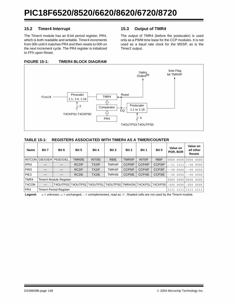
PIC18F6520/8520/6620/8620/6720/8720
15.2 Timer4 Interrupt
The Timer4 module has an 8-bit period register, PR4,which is both readable and writable. Timer4 incrementsfrom 00h until it matches PR4 and then resets to 00h onthe next increment cycle. The PR4 register is initializedto FFh upon Reset.
15.3 Output of TMR4
The output of TMR4 (before the postscaler) is usedonly as a PWM time base for the CCP modules. It is notused as a baud rate clock for the MSSP, as is theTimer2 output.
FIGURE 15-1: TIMER4 BLOCK DIAGRAM
TABLE 15-1: REGISTERS ASSOCIATED WITH TIMER4 AS A TIMER/COUNTER
Name Bit 7 Bit 6 Bit 5 Bit 4 Bit 3 Bit 2 Bit 1 Bit 0Value on
POR, BOR
Value on all other Resets
INTCON GIE/GIEH PEIE/GIEL TMR0IE INT0IE RBIE TMR0IF INT0IF RBIF 0000 0000 0000 0000
IPR3 — — RC2IP TX2IP TMR4IP CCP5IP CCP4IP CCP3IP --11 1111 --00 0000
PIR3 — — RC2IF TX2IF TMR4IF CCP5IF CCP4IF CCP3IF --00 0000 --00 0000
PIE3 — — RC2IE TX2IE TMR4IE CCP5IE CCP4IE CCP3IE --00 0000 --00 0000
TMR4 Timer4 Module Register 0000 0000 0000 0000
T4CON — T4OUTPS3 T4OUTPS2 T4OUTPS1 T4OUTPS0 TMR4ON T4CKPS1 T4CKPS0 -000 0000 -000 0000
PR4 Timer4 Period Register 1111 1111 1111 1111
Legend: x = unknown, u = unchanged, – = unimplemented, read as ‘0’. Shaded cells are not used by the Timer4 module.
Comparator
TMR4Sets Flag
TMR4
Output(1)
Reset
Postscaler
Prescaler
PR4
2
FOSC/4
1:1 to 1:16
1:1, 1:4, 1:16
EQ
4
bit TMR4IF
T4OUTPS3:T4OUTPS0
T4CKPS1:T4CKPS0
DS39609B-page 148 2004 Microchip Technology Inc.

PIC18F6520/8520/6620/8620/6720/8720
16.0 CAPTURE/COMPARE/PWM (CCP) MODULES
The PIC18FXX20 devices all have five CCP (Capture/Compare/PWM) modules. Each module contains a16-bit register, which can operate as a 16-bit Captureregister, a 16-bit Compare register or a Pulse WidthModulation (PWM) Master/Slave Duty Cycle register.Table 16-1 shows the timer resources of the CCPmodule modes.
The operation of all CCP modules are identical, withthe exception of the special event trigger present onCCP1 and CCP2.
For the sake of clarity, CCP module operation in thefollowing sections is described with respect to CCP1.The descriptions can be applied (with the exception ofthe special event triggers) to any of the modules.
REGISTER 16-1: CCPxCON REGISTER
Note: Throughout this section, references toregister and bit names that may be associ-ated with a specific CCP module arereferred to generically by the use of ‘x’ or‘y’ in place of the specific module number.Thus, “CCPxCON” might refer to thecontrol register for CCP1, CCP2, CCP3,CCP4 or CCP5.
U-0 U-0 R/W-0 R/W-0 R/W-0 R/W-0 R/W-0 R/W-0
— — DCxB1 DCxB0 CCPxM3 CCPxM2 CCPxM1 CCPxM0
bit 7 bit 0
bit 7-6 Unimplemented: Read as ‘0’
bit 5-4 DCxB1:DCxB0: PWM Duty Cycle bit 1 and bit 0 for CCP Module xCapture mode:Unused.Compare mode:Unused.PWM mode:These bits are the two Least Significant bits (bit 1 and bit 0) of the 10-bit PWM duty cycle. Theeight Most Significant bits (DCx9:DCx2) of the duty cycle are found in CCPRxL.
bit 3-0 CCPxM3:CCPxM0: CCP Module x Mode Select bits
0000 = Capture/Compare/PWM disabled (resets CCPx module) 0001 = Reserved 0010 = Compare mode, toggle output on match (CCPxIF bit is set) 0011 = Reserved 0100 = Capture mode, every falling edge 0101 = Capture mode, every rising edge0110 = Capture mode, every 4th rising edge 0111 = Capture mode, every 16th rising edge1000 = Compare mode, Initialize CCP pin Low; on compare match, force CCP pin High
(CCPIF bit is set) 1001 = Compare mode, Initialize CCP pin High; on compare match, force CCP pin Low
(CCPIF bit is set) 1010 = Compare mode, Generate software interrupt on compare match (CCPIF bit is set,
(CCP pin is unaffected) 1011 = Compare mode, trigger special event (CCPIF bit is set):
For CCP1 and CCP2: Timer1 or Timer3 is reset on event.For all other modules: CCPx pin is unaffected and is configured as an I/O port (same as CCPxM<3:0> = 1010, above).
11xx = PWM mode
Legend:
R = Readable bit W = Writable bit U = Unimplemented bit, read as ‘0’
- n = Value at POR ‘1’ = Bit is set ‘0’ = Bit is cleared x = Bit is unknown
2004 Microchip Technology Inc. DS39609B-page 149

PIC18F6520/8520/6620/8620/6720/8720
16.1 CCP Module Configuration
Each Capture/Compare/PWM module is associatedwith a control register (generically, CCPxCON) and adata register (CCPRx). The data register, in turn, iscomprised of two 8-bit registers: CCPRxL (low byte)and CCPRxH (high byte). All registers are bothreadable and writable.
16.1.1 CCP MODULES AND TIMER RESOURCES
The CCP modules utilize Timers 1, 2, 3 or 4, dependingon the mode selected. Timer1 and Timer3 are availableto modules in Capture or Compare modes, whileTimer2 and Timer4 are available for modules in PWMmode.
TABLE 16-1: CCP MODE – TIMER RESOURCE
The assignment of a particular timer to a module isdetermined by the Timer-to-CCP Enable bits in theT3CON register (Register 14-1). Depending on theconfiguration selected, up to four timers may be activeat once, with modules in the same configuration(Capture/Compare or PWM) sharing timer resources.The possible configurations are shown in Figure 16-1.
FIGURE 16-1: CCP AND TIMER INTERCONNECT CONFIGURATIONS
CCP Mode Timer Resource
CaptureCompare
PWM
Timer1 or Timer3Timer1 or Timer3Timer2 or Timer4
TMR1
CCP5
TMR2
TMR3
TMR4
CCP4
CCP3
CCP2
CCP1
TMR1
TMR2
TMR3
CCP5
TMR4
CCP4
CCP3
CCP2
CCP1
TMR1
TMR2
TMR3
CCP5
TMR4
CCP4
CCP3
CCP2
CCP1
TMR1
TMR2
TMR3
CCP5
TMR4
CCP4
CCP3
CCP2
CCP1
T3CCP<2:1> = 00 T3CCP<2:1> = 01 T3CCP<2:1> = 10 T3CCP<2:1> = 11
Timer1 is used for all Captureand Compare operations forall CCP modules. Timer2 isused for PWM operations forall CCP modules. Modulesmay share either timerresource as a common timebase.
Timer3 and Timer4 are notavailable.
Timer1 and Timer2 are usedfor Capture and Compare orPWM operations for CCP1only (depending on selectedmode).
All other modules use eitherTimer3 or Timer4. Modulesmay share either timerresource as a common timebase, if they are in Capture/Compare or PWM modes.
Timer1 and Timer2 are usedfor Capture and Compare orPWM operations for CCP1and CCP2 only (depending onthe mode selected for eachmodule). Both modules mayuse a timer as a common timebase if they are both inCapture/Compare or PWMmodes.
The other modules use eitherTimer3 or Timer4. Modulesmay share either timerresource as a common timebase if they are in Capture/Compare or PWM modes.
Timer3 is used for all Captureand Compare operations forall CCP modules. Timer4 isused for PWM operations forall CCP modules. Modulesmay share either timerresource as a common timebase.
Timer1 and Timer2 are notavailable.
DS39609B-page 150 2004 Microchip Technology Inc.

PIC18F6520/8520/6620/8620/6720/8720
16.2 Capture Mode
In Capture mode, CCPR1H:CCPR1L captures the 16-bitvalue of the TMR1 or TMR3 registers when an eventoccurs on pin RC2/CCP1. An event is defined as one ofthe following:
• every falling edge
• every rising edge• every 4th rising edge• every 16th rising edge
The event is selected by control bits, CCP1M3:CCP1M0(CCP1CON<3:0>). When a capture is made, the inter-rupt request flag bit, CCP1IF (PIR1<2>), is set; it mustbe cleared in software. If another capture occurs beforethe value in register CCPR1 is read, the old capturedvalue is overwritten by the new captured value.
16.2.1 CCP PIN CONFIGURATION
In Capture mode, the RC2/CCP1 pin should beconfigured as an input by setting the TRISC<2> bit.
16.2.2 TIMER1/TIMER3 MODE SELECTION
The timers that are to be used with the capture feature(Timer1 and/or Timer3) must be running in Timer mode,or Synchronized Counter mode. In AsynchronousCounter mode, the capture operation may not work. Thetimer to be used with each CCP module is selected in theT3CON register (see Section 16.1.1 “CCP Modulesand Timer Resources”).
16.2.3 SOFTWARE INTERRUPT
When the Capture mode is changed, a false captureinterrupt may be generated. The user should keep bitCCP1IE (PIE1<2>) clear to avoid false interrupts andshould clear the flag bit, CCP1IF, following any suchchange in operating mode.
16.2.4 CCP PRESCALER
There are four prescaler settings, specified by bitsCCP1M3:CCP1M0. Whenever the CCP module isturned off or the CCP module is not in Capture mode,the prescaler counter is cleared. This means that anyReset will clear the prescaler counter.
Switching from one capture prescaler to another maygenerate an interrupt. Also, the prescaler counter willnot be cleared, therefore, the first capture may be froma non-zero prescaler. Example 16-1 shows therecommended method for switching between captureprescalers. This example also clears the prescalercounter and will not generate the “false” interrupt.
EXAMPLE 16-1: CHANGING BETWEEN CAPTURE PRESCALERS
FIGURE 16-2: CAPTURE MODE OPERATION BLOCK DIAGRAM
Note: If the RC2/CCP1 is configured as an out-put, a write to the port can cause a capturecondition.
CLRF CCP1CON, F ; Turn CCP module offMOVLW NEW_CAPT_PS ; Load WREG with the
; new prescaler mode; value and CCP ON
MOVWF CCP1CON ; Load CCP1CON with; this value
CCPR1H CCPR1L
TMR1H TMR1L
Set Flag bit CCP1IF
TMR3Enable
Q’sCCP1CON<3:0>
CCP1 pin
Prescaler÷ 1, 4, 16
andEdge Detect
TMR3H TMR3L
TMR1Enable
T3CCP2
T3CCP2
2004 Microchip Technology Inc. DS39609B-page 151
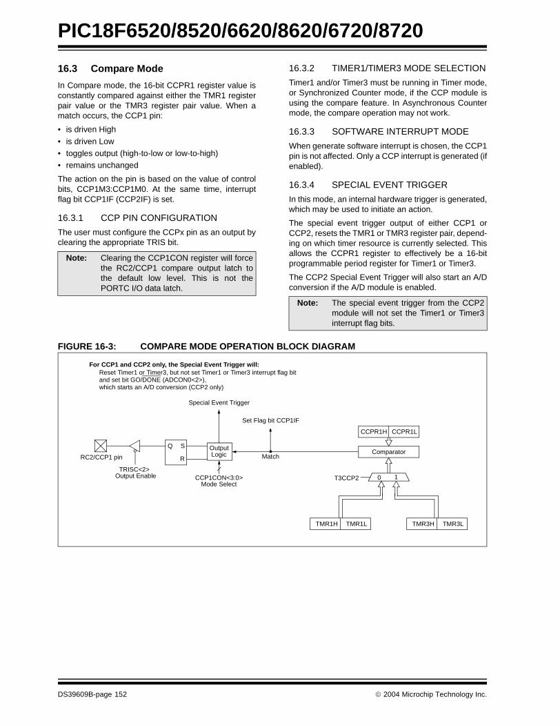
PIC18F6520/8520/6620/8620/6720/8720
16.3 Compare Mode
In Compare mode, the 16-bit CCPR1 register value isconstantly compared against either the TMR1 registerpair value or the TMR3 register pair value. When amatch occurs, the CCP1 pin:
• is driven High
• is driven Low• toggles output (high-to-low or low-to-high) • remains unchanged
The action on the pin is based on the value of controlbits, CCP1M3:CCP1M0. At the same time, interruptflag bit CCP1IF (CCP2IF) is set.
16.3.1 CCP PIN CONFIGURATION
The user must configure the CCPx pin as an output byclearing the appropriate TRIS bit.
16.3.2 TIMER1/TIMER3 MODE SELECTION
Timer1 and/or Timer3 must be running in Timer mode,or Synchronized Counter mode, if the CCP module isusing the compare feature. In Asynchronous Countermode, the compare operation may not work.
16.3.3 SOFTWARE INTERRUPT MODE
When generate software interrupt is chosen, the CCP1pin is not affected. Only a CCP interrupt is generated (ifenabled).
16.3.4 SPECIAL EVENT TRIGGER
In this mode, an internal hardware trigger is generated,which may be used to initiate an action.
The special event trigger output of either CCP1 orCCP2, resets the TMR1 or TMR3 register pair, depend-ing on which timer resource is currently selected. Thisallows the CCPR1 register to effectively be a 16-bitprogrammable period register for Timer1 or Timer3.
The CCP2 Special Event Trigger will also start an A/Dconversion if the A/D module is enabled.
FIGURE 16-3: COMPARE MODE OPERATION BLOCK DIAGRAM
Note: Clearing the CCP1CON register will forcethe RC2/CCP1 compare output latch tothe default low level. This is not thePORTC I/O data latch.
Note: The special event trigger from the CCP2module will not set the Timer1 or Timer3interrupt flag bits.
CCPR1H CCPR1L
TMR1H TMR1L
ComparatorQ S
R
OutputLogic
Special Event Trigger
Set Flag bit CCP1IF
MatchRC2/CCP1 pin
TRISC<2>CCP1CON<3:0>
Mode SelectOutput Enable
For CCP1 and CCP2 only, the Special Event Trigger will:Reset Timer1 or Timer3, but not set Timer1 or Timer3 interrupt flag bitand set bit GO/DONE (ADCON0<2>),which starts an A/D conversion (CCP2 only)
TMR3H TMR3L
T3CCP2 10
DS39609B-page 152 2004 Microchip Technology Inc.

PIC18F6520/8520/6620/8620/6720/8720
TABLE 16-2: REGISTERS ASSOCIATED WITH CAPTURE, COMPARE, TIMER1 AND TIMER3
Name Bit 7 Bit 6 Bit 5 Bit 4 Bit 3 Bit 2 Bit 1 Bit 0Value on
POR, BOR
Value onall otherResets
INTCON GIE/GIEH PEIE/GIEL TMR0IE INT0IE RBIE TMR0IF INT0IF RBIF 0000 0000 0000 0000
RCON IPEN — — RI TO PD POR BOR 0--1 11qq 0--q qquu
PIR1 PSPIF ADIF RCIF TXIF SSPIF CCP1IF TMR2IF TMR1IF 0000 0000 0000 0000
PIE1 PSPIE ADIE RCIE TXIE SSPIE CCP1IE TMR2IE TMR1IE 0000 0000 0000 0000
IPR1 PSPIP ADIP RCIP TXIP SSPIP CCP1IP TMR2IP TMR1IP 0111 1111 0111 1111
PIR2 — CMIE — EEIE BCLIF LVDIF TMR3IF CCP2IF -0-0 0000 ---0 0000
PIE2 — CMIF — EEIF BCLIE LVDIE TMR3IE CCP2IE -0-0 0000 ---0 0000
IPR2 — CMIP — EEIP BCLIP LVDIP TMR3IP CCP2IP -1-1 1111 ---1 1111
PIR3 — — RC2IF TX2IF TMR4IF CCP5IF CCP4IF CCP3IF --00 0000 --00 0000
PIE3 — — RC2IE TX2IE TMR4IE CCP5IE CCP4IE CCP3IE --00 0000 --00 0000
IPR3 — — RC2IP TX2IP TMR4IP CCP5IP CCP4IP CCP3IP --11 1111 --11 1111
TRISC PORTC Data Direction Register 1111 1111 1111 1111
TMR1L Holding Register for the Least Significant Byte of the 16-bit TMR1 Register xxxx xxxx uuuu uuuu
TMR1H Holding Register for the Most Significant Byte of the 16-bit TMR1 Register xxxx xxxx uuuu uuuu
T1CON RD16 — T1CKPS1 T1CKPS0 T1OSCEN T1SYNC TMR1CS TMR1ON 0-00 0000 u-uu uuuu
TMR3H Timer3 Register High Byte xxxx xxxx uuuu uuuu
TMR3L Timer3 Register Low Byte xxxx xxxx uuuu uuuu
T3CON RD16 T3CCP2 T3CKPS1 T3CKPS0 T3CCP1 T3SYNC TMR3CS TMR3ON 0000 0000 uuuu uuuu
CCPRxL(1) Capture/Compare/PWM Register x (LSB) xxxx xxxx uuuu uuuu
CCPRxH(1) Capture/Compare/PWM Register x (MSB) xxxx xxxx uuuu uuuu
CCPxCON(1) — — DCxB1 DCxB0 CCPxM3 CCPxM2 CCPxM1 CCPxM0 --00 0000 --00 0000
Legend: x = unknown, u = unchanged, – = unimplemented, read as ‘0’. Shaded cells are not used by Capture and Compare, Timer1 or Timer3.
Note 1: Generic term for all of the identical registers of this name for all CCP modules, where ‘x’ identifies the individual module (CCP1 through CCP5). Bit assignments and Reset values for all registers of the same generic name are identical.
2004 Microchip Technology Inc. DS39609B-page 153

PIC18F6520/8520/6620/8620/6720/8720
16.4 PWM Mode
In Pulse Width Modulation (PWM) mode, the CCP1 pinproduces up to a 10-bit resolution PWM output. Sincethe CCP1 pin is multiplexed with the PORTC data latch,the TRISC<2> bit must be cleared to make the CCP1pin an output.
Figure 16-4 shows a simplified block diagram of theCCP module in PWM mode.
For a step-by-step procedure on how to set up the CCPmodule for PWM operation, see Section 16.4.3“Setup for PWM Operation”.
FIGURE 16-4: SIMPLIFIED PWM BLOCK DIAGRAM
A PWM output (Figure 16-5) has a time base (period)and a time that the output stays high (duty cycle).The frequency of the PWM is the inverse of the period(1/period).
FIGURE 16-5: PWM OUTPUT
16.4.1 PWM PERIOD
The PWM period is specified by writing to the PR2register. The PWM period can be calculated using thefollowing formula:
EQUATION 16-1:
PWM frequency is defined as 1/[PWM period].
When TMR2 is equal to PR2, the following three eventsoccur on the next increment cycle:
• TMR2 is cleared• The CCP1 pin is set (exception: if PWM duty
cycle = 0%, the CCP1 pin will not be set)
• The PWM duty cycle is latched from CCPR1L into CCPR1H
16.4.2 PWM DUTY CYCLE
The PWM duty cycle is specified by writing to theCCPR1L register and to the CCP1CON<5:4> bits. Upto 10-bit resolution is available. The CCPR1L containsthe eight MSbs and the CCP1CON<5:4> contains thetwo LSbs. This 10-bit value is represented byCCPR1L:CCP1CON<5:4>. The following equation isused to calculate the PWM duty cycle in time:
EQUATION 16-2:
CCPR1L and CCP1CON<5:4> can be written to at anytime, but the duty cycle value is not latched intoCCPR1H until after a match between PR2 and TMR2occurs (i.e., the period is complete). In PWM mode,CCPR1H is a read-only register.
The CCPR1H register and a 2-bit internal latch areused to double-buffer the PWM duty cycle. Thisdoublebuffering is essential for glitchless PWMoperation.
When the CCPR1H and 2-bit latch match TMR2, con-catenated with an internal 2-bit Q clock or 2 bits of theTMR2 prescaler, the CCP1 pin is cleared.
Note: Clearing the CCP1CON register will forcethe CCP1 PWM output latch to the defaultlow level. This is not the PORTC I/O datalatch.
CCPR1L
CCPR1H (Slave)
Comparator
TMR2
Comparator
PR2
(Note 1)
R Q
S
Duty Cycle Registers CCP1CON<5:4>
Clear Timer,CCP1 pin and latch D.C.
TRISC<2>
RC2/CCP1
Note 1: 8-bit timer is concatenated with 2-bit internal Qclock or 2 bits of the prescaler to create 10-bittime base.
Period
Duty Cycle
TMR2 = PR2
TMR2 = Duty Cycle
TMR2 = PR2
Note: The Timer2 and Timer4 postscalers (seeSection 13.0 “Timer2 Module”) are notused in the determination of the PWMfrequency. The postscaler could be usedto have a servo update rate at a differentfrequency than the PWM output.
PWM Period = (PR2) + 1] • 4 • TOSC •(TMR2 Prescale Value)
PWM Duty Cycle = (CCPR1L:CCP1CON<5:4>) •TOSC • (TMR2 Prescale Value)
DS39609B-page 154 2004 Microchip Technology Inc.

PIC18F6520/8520/6620/8620/6720/8720
The maximum PWM resolution (bits) for a given PWMfrequency is given by the equation:
EQUATION 16-3:
16.4.3 SETUP FOR PWM OPERATION
The following steps should be taken when configuringthe CCP module for PWM operation:
1. Set the PWM period by writing to the PR2register.
2. Set the PWM duty cycle by writing to theCCPR1L register and CCP1CON<5:4> bits.
3. Make the CCP1 pin an output by clearing theTRISC<2> bit.
4. Set the TMR2 prescale value and enable Timer2by writing to T2CON.
5. Configure the CCP1 module for PWM operation.
TABLE 16-3: EXAMPLE PWM FREQUENCIES AND RESOLUTIONS AT 40 MHz
TABLE 16-4: REGISTERS ASSOCIATED WITH PWM, TIMER2 AND TIMER4
Note: If the PWM duty cycle value is longer thanthe PWM period, the CCP1 pin will not becleared.
FOSC
FPWM--------------- log
2( )log-----------------------------bits=PWM Resolution (max)
PWM Frequency 2.44 kHz 9.77 kHz 39.06 kHz 156.25 kHz 312.50 kHz 416.67 kHz
Timer Prescaler (1, 4, 16) 16 4 1 1 1 1
PR2 Value FFh FFh FFh 3Fh 1Fh 17h
Maximum Resolution (bits) 14 → 10 12 → 10 10 8 7 6.58
Name Bit 7 Bit 6 Bit 5 Bit 4 Bit 3 Bit 2 Bit 1 Bit 0Value on
POR, BOR
Value on all otherResets
INTCON GIE/GIEH PEIE/GIEL TMR0IE INT0IE RBIE TMR0IF INT0IF RBIF 0000 0000 0000 0000
RCON IPEN — — RI TO PD POR BOR 0--1 11qq 0--q qquu
PIR1 PSPIF ADIF RCIF TXIF SSPIF CCP1IF TMR2IF TMR1IF 0000 0000 0000 0000
PIE1 PSPIE ADIE RCIE TXIE SSPIE CCP1IE TMR2IE TMR1IE 0000 0000 0000 0000
IPR1 PSPIP ADIP RCIP TXIP SSPIP CCP1IP TMR2IP TMR1IP 0111 1111 0111 1111
PIR2 — CMIE — EEIE BCLIF LVDIF TMR3IF CCP2IF -0-0 0000 ---0 0000
PIE2 — CMIF — EEIF BCLIE LVDIE TMR3IE CCP2IE -0-0 0000 ---0 0000
IPR2 — CMIP — EEIP BCLIP LVDIP TMR3IP CCP2IP -1-1 1111 ---1 1111
PIR3 — — RC2IF TX2IF TMR4IF CCP5IF CCP4IF CCP3IF --00 0000 --00 0000
PIE3 — — RC2IE TX2IE TMR4IE CCP5IE CCP4IE CCP3IE --00 0000 --00 0000
IPR3 — — RC2IP TX2IP TMR4IP CCP5IP CCP4IP CCP3IP --11 1111 --11 1111
TMR2 Timer2 Module Register 0000 0000 0000 0000
PR2 Timer2 Module Period Register 1111 1111 1111 1111
T2CON — T2OUTPS3 T2OUTPS2 T2OUTPS1 T2OUTPS0 TMR2ON T2CKPS1 T2CKPS0 -000 0000 -000 0000
T3CON RD16 T3CCP2 T3CKPS1 T3CKPS0 T3CCP1 T3SYNC TMR3CS TMR3ON 0000 0000 uuuu uuuu
TMR4 Timer4 Register 0000 0000 uuuu uuuu
PR4 Timer4 Period Register 1111 1111 uuuu uuuu
T4CON — T4OUTPS3 T4OUTPS2 T4OUTPS1 T4OUTPS0 TMR4ON T4CKPS1 T4CKPS0 -000 0000 uuuu uuuu
CCPRxL(1) Capture/Compare/PWM Register x (LSB) xxxx xxxx uuuu uuuu
CCPRxH(1) Capture/Compare/PWM Register x (MSB) xxxx xxxx uuuu uuuu
CCPxCON(1) — — DCxB1 DCxB0 CCPxM3 CCPxM2 CCPxM1 CCPxM0 --00 0000 --00 0000
Legend: x = unknown, u = unchanged, – = unimplemented, read as ‘0’. Shaded cells are not used by PWM, Timer2, or Timer4.Note 1: Generic term for all of the identical registers of this name for all CCP modules, where ‘x’ identifies the individual module
(CCP1 through CCP5). Bit assignments and Reset values for all registers of the same generic name are identical.
2004 Microchip Technology Inc. DS39609B-page 155

PIC18F6520/8520/6620/8620/6720/8720
NOTES:
DS39609B-page 156 2004 Microchip Technology Inc.

PIC18F6520/8520/6620/8620/6720/8720
17.0 MASTER SYNCHRONOUS SERIAL PORT (MSSP) MODULE
17.1 Master SSP (MSSP) Module Overview
The Master Synchronous Serial Port (MSSP) module isa serial interface, useful for communicating with otherperipheral or microcontroller devices. These peripheraldevices may be serial EEPROMs, shift registers, dis-play drivers, A/D converters, etc. The MSSP modulecan operate in one of two modes:
• Serial Peripheral Interface (SPI)• Inter-Integrated Circuit (I2C)
- Full Master mode- Slave mode (with general address call)
The I2C interface supports the following modes inhardware:
• Master mode• Multi-Master mode• Slave mode
17.2 Control Registers
The MSSP module has three associated registers.These include a status register (SSPSTAT) and twocontrol registers (SSPCON1 and SSPCON2). The useof these registers and their individual configuration bitsdiffer significantly, depending on whether the MSSPmodule is operated in SPI or I2C mode.
Additional details are provided under the individualsections.
17.3 SPI Mode
The SPI mode allows 8 bits of data to be synchronouslytransmitted and received simultaneously. All four modesof SPI are supported. To accomplish communication,typically three pins are used:
• Serial Data Out (SDO) – RC5/SDO
• Serial Data In (SDI) – RC4/SDI/SDA• Serial Clock (SCK) – RC3/SCK/SCL
Additionally, a fourth pin may be used when in a Slavemode of operation:
• Slave Select (SS) – RF7/SS
Figure 17-1 shows the block diagram of the MSSPmodule when operating in SPI mode.
FIGURE 17-1: MSSP BLOCK DIAGRAM (SPI MODE)
( )
Read Write
InternalData Bus
SSPSR reg
SSPM3:SSPM0
bit0 ShiftClock
SS ControlEnable
EdgeSelect
Clock Select
TMR2 Output
TOSCPrescaler4, 16, 64
2EdgeSelect
2
4
Data to TX/RX in SSPSRTRIS bit
2SMP:CKE
RC5/SDO
SSPBUF reg
RC4/SDI/SDA
RF7/SS
RC3/SCK/SCL
2004 Microchip Technology Inc. DS39609B-page 157

PIC18F6520/8520/6620/8620/6720/8720
17.3.1 REGISTERS
The MSSP module has four registers for SPI modeoperation. These are:
• MSSP Control Register 1 (SSPCON1)• MSSP Status Register (SSPSTAT)
• Serial Receive/Transmit Buffer (SSPBUF)• MSSP Shift Register (SSPSR) – Not directly
accessible
SSPCON1 and SSPSTAT are the control and statusregisters in SPI mode operation. The SSPCON1 regis-ter is readable and writable. The lower 6 bits of theSSPSTAT are read-only. The upper two bits of theSSPSTAT are read/write.
SSPSR is the shift register used for shifting data in orout. SSPBUF is the buffer register to which data bytesare written to or read from.
In receive operations, SSPSR and SSPBUF togethercreate a double-buffered receiver. When SSPSRreceives a complete byte, it is transferred to SSPBUFand the SSPIF interrupt is set.
During transmission, the SSPBUF is not double-buffered. A write to SSPBUF will write to both SSPBUFand SSPSR.
REGISTER 17-1: SSPSTAT: MSSP STATUS REGISTER (SPI MODE)R/W-0 R/W-0 R-0 R-0 R-0 R-0 R-0 R-0
SMP CKE D/A P S R/W UA BF
bit 7 bit 0
bit 7 SMP: Sample bitSPI Master mode:1 = Input data sampled at end of data output time0 = Input data sampled at middle of data output timeSPI Slave mode:SMP must be cleared when SPI is used in Slave mode.
bit 6 CKE: SPI Clock Select bit
1 = Transmit occurs on transition from active to Idle clock state0 = Transmit occurs on transition from Idle to active clock state
Note: Polarity of clock state is set by the CKP bit (SSPCON1<4>).
bit 5 D/A: Data/Address bit Used in I2C mode only.
bit 4 P: Stop bit Used in I2C mode only. This bit is cleared when the MSSP module is disabled, SSPEN is cleared.
bit 3 S: Start bitUsed in I2C mode only.
bit 2 R/W: Read/Write bit informationUsed in I2C mode only.
bit 1 UA: Update Address bitUsed in I2C mode only.
bit 0 BF: Buffer Full Status bit (Receive mode only)1 = Receive complete, SSPBUF is full 0 = Receive not complete, SSPBUF is empty
Legend:
R = Readable bit W = Writable bit U = Unimplemented bit, read as ‘0’
- n = Value at POR ‘1’ = Bit is set ‘0’ = Bit is cleared x = Bit is unknown
DS39609B-page 158 2004 Microchip Technology Inc.

PIC18F6520/8520/6620/8620/6720/8720
REGISTER 17-2: SSPCON1: MSSP CONTROL REGISTER1 (SPI MODE)R/W-0 R/W-0 R/W-0 R/W-0 R/W-0 R/W-0 R/W-0 R/W-0
WCOL SSPOV SSPEN CKP SSPM3 SSPM2 SSPM1 SSPM0
bit 7 bit 0
bit 7 WCOL: Write Collision Detect bit (Transmit mode only)1 = The SSPBUF register is written while it is still transmitting the previous word
(must be cleared in software) 0 = No collision
bit 6 SSPOV: Receive Overflow Indicator bit SPI Slave mode:
1 = A new byte is received while the SSPBUF register is still holding the previous data. In caseof overflow, the data in SSPSR is lost. Overflow can only occur in Slave mode. The usermust read the SSPBUF, even if only transmitting data, to avoid setting overflow(must be cleared in software).
0 = No overflow
Note: In Master mode, the overflow bit is not set, since each new reception (andtransmission) is initiated by writing to the SSPBUF register.
bit 5 SSPEN: Synchronous Serial Port Enable bit 1 = Enables serial port and configures SCK, SDO, SDI and SS as serial port pins 0 = Disables serial port and configures these pins as I/O port pins
Note: When enabled, these pins must be properly configured as input or output.
bit 4 CKP: Clock Polarity Select bit
1 = Idle state for clock is a high level 0 = Idle state for clock is a low level
bit 3-0 SSPM3:SSPM0: Synchronous Serial Port Mode Select bits0101 = SPI Slave mode, clock = SCK pin, SS pin control disabled, SS can be used as I/O pin 0100 = SPI Slave mode, clock = SCK pin, SS pin control enabled0011 = SPI Master mode, clock = TMR2 output/2 0010 = SPI Master mode, clock = FOSC/64 0001 = SPI Master mode, clock = FOSC/16 0000 = SPI Master mode, clock = FOSC/4
Note: Bit combinations not specifically listed here are either reserved, or implemented inI2C mode only.
Legend:
R = Readable bit W = Writable bit U = Unimplemented bit, read as ‘0’
- n = Value at POR ‘1’ = Bit is set ‘0’ = Bit is cleared x = Bit is unknown
2004 Microchip Technology Inc. DS39609B-page 159

PIC18F6520/8520/6620/8620/6720/8720
17.3.2 OPERATION
When initializing the SPI, several options need to bespecified. This is done by programming the appropriatecontrol bits (SSPCON1<5:0> and SSPSTAT<7:6>).These control bits allow the following to be specified:
• Master mode (SCK is the clock output)
• Slave mode (SCK is the clock input)• Clock Polarity (Idle state of SCK)• Data input sample phase (middle or end of data
output time)• Clock edge (output data on rising/falling edge of
SCK)• Clock Rate (Master mode only)
• Slave Select mode (Slave mode only)
The MSSP consists of a Transmit/Receive Shift Regis-ter (SSPSR) and a Buffer register (SSPBUF). TheSSPSR shifts the data in and out of the device, MSbfirst. The SSPBUF holds the data that was written to theSSPSR until the received data is ready. Once the 8 bitsof data have been received, that byte is moved to theSSPBUF register. Then, the Buffer Full detect bit, BF(SSPSTAT<0>) and the interrupt flag bit, SSPIF, areset. This double-buffering of the received data(SSPBUF) allows the next byte to start reception before
reading the data that was just received. Any write to theSSPBUF register during transmission/reception of datawill be ignored and the Write Collision detect bit, WCOL(SSPCON1<7>), will be set. User software must clearthe WCOL bit so that it can be determined if the follow-ing write(s) to the SSPBUF register completedsuccessfully.
When the application software is expecting to receivevalid data, the SSPBUF should be read before the nextbyte of data to transfer is written to the SSPBUF. BufferFull bit, BF (SSPSTAT<0>), indicates when SSPBUFhas been loaded with the received data (transmissionis complete). When the SSPBUF is read, the BF bit iscleared. This data may be irrelevant if the SPI is only atransmitter. Generally, the MSSP interrupt is used todetermine when the transmission/reception has com-pleted. The SSPBUF must be read and/or written. If theinterrupt method is not going to be used, then softwarepolling can be done to ensure that a write collision doesnot occur. Example 17-1 shows the loading of theSSPBUF (SSPSR) for data transmission.
The SSPSR is not directly readable or writable and canonly be accessed by addressing the SSPBUF register.Additionally, the MSSP Status register (SSPSTAT)indicates the various status conditions.
EQUATION 17-1: LOADING THE SSPBUF (SSPSR) REGISTER LOOP BTFSS SSPSTAT, BF ;Has data been received (transmit complete)? BRA LOOP ;No MOVF SSPBUF, W ;WREG reg = contents of SSPBUF
MOVWF RXDATA ;Save in user RAM, if data is meaningful
MOVF TXDATA, W ;W reg = contents of TXDATA MOVWF SSPBUF ;New data to transmit
DS39609B-page 160 2004 Microchip Technology Inc.

PIC18F6520/8520/6620/8620/6720/8720
17.3.3 ENABLING SPI I/O
To enable the serial port, SSP Enable bit, SSPEN(SSPCON1<5>), must be set. To reset or reconfigureSPI mode, clear the SSPEN bit, reinitialize theSSPCON registers and then set the SSPEN bit. Thisconfigures the SDI, SDO, SCK and SS pins as serialport pins. For the pins to behave as the serial port func-tion, some must have their data direction bits (in theTRIS register) appropriately programmed as follows:
• SDI is automatically controlled by the SPI module • SDO must have TRISC<5> bit cleared
• SCK (Master mode) must have TRISC<3> bit cleared
• SCK (Slave mode) must have TRISC<3> bit set • SS must have TRISF<7> bit set
Any serial port function that is not desired may beoverridden by programming the corresponding datadirection (TRIS) register to the opposite value.
17.3.4 TYPICAL CONNECTION
Figure 17-2 shows a typical connection between twomicrocontrollers. The master controller (Processor 1)initiates the data transfer by sending the SCK signal.Data is shifted out of both shift registers on their pro-grammed clock edge and latched on the opposite edgeof the clock. Both processors should be programmed tothe same Clock Polarity (CKP), then both controllerswould send and receive data at the same time.Whether the data is meaningful (or dummy data)depends on the application software. This leads tothree scenarios for data transmission:
• Master sends data – Slave sends dummy data• Master sends data – Slave sends data
• Master sends dummy data – Slave sends data
FIGURE 17-2: SPI MASTER/SLAVE CONNECTION
Serial Input Buffer(SSPBUF)
Shift Register(SSPSR)
MSb LSb
SDO
SDI
PROCESSOR 1
SCK
SPI Master SSPM3:SSPM0 = 00xxb
Serial Input Buffer(SSPBUF)
Shift Register(SSPSR)
LSbMSb
SDI
SDO
PROCESSOR 2
SCK
SPI Slave SSPM3:SSPM0 = 010xb
Serial Clock
2004 Microchip Technology Inc. DS39609B-page 161

PIC18F6520/8520/6620/8620/6720/8720
17.3.5 MASTER MODE
The master can initiate the data transfer at any timebecause it controls the SCK. The master determineswhen the slave (Processor 2, Figure 17-2) is tobroadcast data by the software protocol.
In Master mode, the data is transmitted/received assoon as the SSPBUF register is written to. If the SPI isonly going to receive, the SDO output could be dis-abled (programmed as an input). The SSPSR registerwill continue to shift in the signal present on the SDI pinat the programmed clock rate. As each byte isreceived, it will be loaded into the SSPBUF register asif a normal received byte (interrupts and status bitsappropriately set). This could be useful in receiverapplications as a “Line Activity Monitor” mode.
The clock polarity is selected by appropriately program-ming the CKP bit (SSPCON1<4>). This then, wouldgive waveforms for SPI communication, as shown in
Figure 17-3, Figure 17-5 and Figure 17-6, where theMSB is transmitted first. In Master mode, the SPI clockrate (bit rate) is user-programmable to be one of thefollowing:
• FOSC/4 (or TCY)• FOSC/16 (or 4 • TCY)
• FOSC/64 (or 16 • TCY)• Timer2 output/2
This allows a maximum data rate (at 40 MHz) of10.00 Mbps.
Figure 17-3 shows the waveforms for Master mode.When the CKE bit is set, the SDO data is valid beforethere is a clock edge on SCK. The change of the inputsample is shown based on the state of the SMP bit. Thetime when the SSPBUF is loaded with the receiveddata is shown.
FIGURE 17-3: SPI MODE WAVEFORM (MASTER MODE)
SCK(CKP = 0
SCK(CKP = 1
SCK(CKP = 0
SCK(CKP = 1
4 ClockModes
InputSample
InputSample
SDI
bit 7 bit 0
SDO bit 7 bit 6 bit 5 bit 4 bit 3 bit 2 bit 1 bit 0
bit 7
SDI
SSPIF
(SMP = 1)
(SMP = 0)
(SMP = 1)
CKE = 1)
CKE = 0)
CKE = 1)
CKE = 0)
(SMP = 0)
Write toSSPBUF
SSPSR toSSPBUF
SDO bit 7 bit 6 bit 5 bit 4 bit 3 bit 2 bit 1 bit 0
(CKE = 0)
(CKE = 1)
Next Q4 cycleafter Q2↓
bit 0
DS39609B-page 162 2004 Microchip Technology Inc.

PIC18F6520/8520/6620/8620/6720/8720
17.3.6 SLAVE MODE
In Slave mode, the data is transmitted and received asthe external clock pulses appear on SCK. When thelast bit is latched, the SSPIF interrupt flag bit is set.
While in Slave mode, the external clock is supplied bythe external clock source on the SCK pin. This externalclock must meet the minimum high and low times asspecified in the electrical specifications.
While in Sleep mode, the slave can transmit/receivedata. When a byte is received, the device will wake-upfrom Sleep.
17.3.7 SLAVE SELECT SYNCHRONIZATION
The SS pin allows a Synchronous Slave mode. TheSPI must be in Slave mode with SS pin control enabled(SSPCON1<3:0> = 04h). The pin must not be drivenlow for the SS pin to function as an input. The DataLatch must be high. When the SS pin is low, transmis-sion and reception are enabled and the SDO pin isdriven. When the SS pin goes high, the SDO pin is no
longer driven, even if in the middle of a transmittedbyte and becomes a floating output. External pull-up/pull-down resistors may be desirable, depending on theapplication.
When the SPI module resets, the bit counter is forcedto ‘0’. This can be done by either forcing the SS pin toa high level or clearing the SSPEN bit.
To emulate two-wire communication, the SDO pin canbe connected to the SDI pin. When the SPI needs tooperate as a receiver, the SDO pin can be configuredas an input. This disables transmissions from the SDO.The SDI can always be left as an input (SDI function),since it cannot create a bus conflict.
FIGURE 17-4: SLAVE SYNCHRONIZATION WAVEFORM
Note 1: When the SPI is in Slave mode with SS pincontrol enabled (SSPCON<3:0> = 0100),the SPI module will reset if the SS pin is setto VDD.
2: If the SPI is used in Slave mode with CKEset, then the SS pin control must beenabled.
SCK(CKP = 1
SCK(CKP = 0
InputSample
SDI
bit 7
SDO bit 7 bit 6 bit 7
SSPIFInterrupt
(SMP = 0)
CKE = 0)
CKE = 0)
(SMP = 0)
Write toSSPBUF
SSPSR toSSPBUF
SS
Flag
bit 0
bit 7
bit 0
Next Q4 cycleafter Q2↓
2004 Microchip Technology Inc. DS39609B-page 163

PIC18F6520/8520/6620/8620/6720/8720
FIGURE 17-5: SPI MODE WAVEFORM (SLAVE MODE WITH CKE = 0)
FIGURE 17-6: SPI MODE WAVEFORM (SLAVE MODE WITH CKE = 1)
SCK(CKP = 1
SCK(CKP = 0
InputSample
SDI
bit 7
SDO bit 7 bit 6 bit 5 bit 4 bit 3 bit 2 bit 1 bit 0
SSPIFInterrupt
(SMP = 0)
CKE = 0)
CKE = 0)
(SMP = 0)
Write toSSPBUF
SSPSR toSSPBUF
SS
Flag
Optional
Next Q4 cycleafter Q2↓
bit 0
SCK(CKP = 1
SCK(CKP = 0
InputSample
SDI
bit 7 bit 0
SDO bit 7 bit 6 bit 5 bit 4 bit 3 bit 2 bit 1 bit 0
SSPIFInterrupt
(SMP = 0)
CKE = 1)
CKE = 1)
(SMP = 0)
Write toSSPBUF
SSPSR toSSPBUF
SS
Flag
Not Optional
Next Q4 cycleafter Q2↓
DS39609B-page 164 2004 Microchip Technology Inc.

PIC18F6520/8520/6620/8620/6720/8720
17.3.8 SLEEP OPERATION
In Master mode, all module clocks are halted and thetransmission/reception will remain in that state until thedevice wakes from Sleep. After the device returns tonormal mode, the module will continue to transmit/receive data.
In Slave mode, the SPI Transmit/Receive Shift registeroperates asynchronously to the device. This allows thedevice to be placed in Sleep mode and data to beshifted into the SPI Transmit/Receive Shift register.When all 8 bits have been received, the MSSP interruptflag bit will be set and if enabled, will wake the devicefrom Sleep.
17.3.9 EFFECTS OF A RESET
A Reset disables the MSSP module and terminates thecurrent transfer.
17.3.10 BUS MODE COMPATIBILITY
Table 17-1 shows the compatibility between thestandard SPI modes and the states of the CKP andCKE control bits.
TABLE 17-1: SPI BUS MODES
There is also an SMP bit, which controls when the datais sampled.
TABLE 17-2: REGISTERS ASSOCIATED WITH SPI OPERATION
Standard SPI Mode Terminology
Control Bits State
CKP CKE
0, 0 0 1
0, 1 0 0
1, 0 1 1
1, 1 1 0
Name Bit 7 Bit 6 Bit 5 Bit 4 Bit 3 Bit 2 Bit 1 Bit 0Value on
POR, BOR
Value onall otherResets
INTCON GIE/GIEH PEIE/GIEL TMR0IE INT0IE RBIE TMR0IF INT0IF RBIF 0000 0000 0000 0000
PIR1 PSPIF ADIF RCIF TXIF SSPIF CCP1IF TMR2IF TMR1IF 0000 0000 0000 0000
PIE1 PSPIE ADIE RCIE TXIE SSPIE CCP1IE TMR2IE TMR1IE 0000 0000 0000 0000
IPR1 PSPIP ADIP RCIP TXIP SSPIP CCP1IP TMR2IP TMR1IP 0111 1111 0111 1111
TRISC PORTC Data Direction Register 1111 1111 1111 1111
TRISF TRISF7 TRISF6 TRISF5 TRISF4 TRISF3 TRISF2 TRISF1 TRISF0 1111 1111 uuuu uuuu
SSPBUF Synchronous Serial Port Receive Buffer/Transmit Register xxxx xxxx uuuu uuuu
SSPCON WCOL SSPOV SSPEN CKP SSPM3 SSPM2 SSPM1 SSPM0 0000 0000 0000 0000
SSPSTAT SMP CKE D/A P S R/W UA BF 0000 0000 0000 0000
Legend: x = unknown, u = unchanged, – = unimplemented, read as ‘0’. Shaded cells are not used by the MSSP in SPI mode.
2004 Microchip Technology Inc. DS39609B-page 165

PIC18F6520/8520/6620/8620/6720/8720
17.4 I2C Mode
The MSSP module in I2C mode fully implements allmaster and slave functions (including general call sup-port) and provides interrupts on Start and Stop bits inhardware to determine a free bus (multi-masterfunction). The MSSP module implements the standardmode specifications, as well as 7-bit and 10-bitaddressing.
Two pins are used for data transfer:
• Serial clock (SCL) – RC3/SCK/SCL
• Serial data (SDA) – RC4/SDI/SDA
The user must configure these pins as inputs or outputsthrough the TRISC<4:3> bits.
FIGURE 17-7: MSSP BLOCK DIAGRAM (I2C MODE)
17.4.1 REGISTERS
The MSSP module has six registers for I2C operation.These are:
• MSSP Control Register 1 (SSPCON1)• MSSP Control Register 2 (SSPCON2)
• MSSP Status Register (SSPSTAT)• Serial Receive/Transmit Buffer (SSPBUF)• MSSP Shift Register (SSPSR) – Not directly
accessible• MSSP Address Register (SSPADD)
SSPCON, SSPCON2 and SSPSTAT are the controland status registers in I2C mode operation. TheSSPCON and SSPCON2 registers are readable andwritable. The lower six bits of the SSPSTAT areread-only. The upper two bits of the SSPSTAT areread/write.
SSPSR is the shift register used for shifting data in orout. SSPBUF is the buffer register to which data bytesare written to or read from.
SSPADD register holds the slave device addresswhen the SSP is configured in I2C Slave mode. Whenthe SSP is configured in Master mode, the lowerseven bits of SSPADD act as the Baud RateGenerator reload value.
In receive operations, SSPSR and SSPBUF together,create a double-buffered receiver. When SSPSRreceives a complete byte, it is transferred to SSPBUFand the SSPIF interrupt is set.
During transmission, the SSPBUF is not double-buffered. A write to SSPBUF will write to both SSPBUFand SSPSR.
Read Write
SSPSR reg
Match Detect
SSPADD reg
Start and Stop bit Detect
SSPBUF reg
InternalData Bus
Addr Match
Set, ResetS, P bits
(SSPSTAT reg)
RC3/SCK/SCL
RC4/
ShiftClock
MSbSDI/
LSb
SDA
DS39609B-page 166 2004 Microchip Technology Inc.
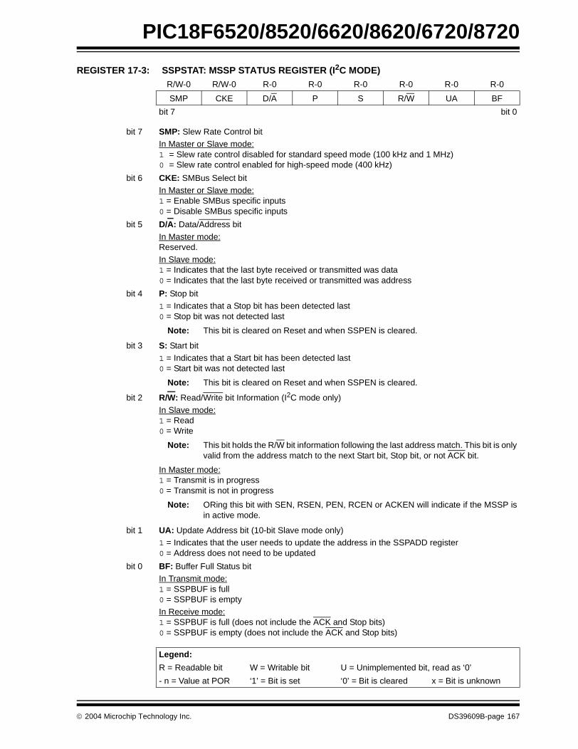
PIC18F6520/8520/6620/8620/6720/8720
REGISTER 17-3: SSPSTAT: MSSP STATUS REGISTER (I2C MODE)R/W-0 R/W-0 R-0 R-0 R-0 R-0 R-0 R-0
SMP CKE D/A P S R/W UA BF
bit 7 bit 0
bit 7 SMP: Slew Rate Control bitIn Master or Slave mode: 1 = Slew rate control disabled for standard speed mode (100 kHz and 1 MHz) 0 = Slew rate control enabled for high-speed mode (400 kHz)
bit 6 CKE: SMBus Select bitIn Master or Slave mode:1 = Enable SMBus specific inputs 0 = Disable SMBus specific inputs
bit 5 D/A: Data/Address bit
In Master mode:Reserved.
In Slave mode:1 = Indicates that the last byte received or transmitted was data0 = Indicates that the last byte received or transmitted was address
bit 4 P: Stop bit1 = Indicates that a Stop bit has been detected last0 = Stop bit was not detected last
Note: This bit is cleared on Reset and when SSPEN is cleared.
bit 3 S: Start bit1 = Indicates that a Start bit has been detected last 0 = Start bit was not detected last
Note: This bit is cleared on Reset and when SSPEN is cleared.
bit 2 R/W: Read/Write bit Information (I2C mode only)
In Slave mode:1 = Read0 = Write
Note: This bit holds the R/W bit information following the last address match. This bit is onlyvalid from the address match to the next Start bit, Stop bit, or not ACK bit.
In Master mode:1 = Transmit is in progress0 = Transmit is not in progress
Note: ORing this bit with SEN, RSEN, PEN, RCEN or ACKEN will indicate if the MSSP isin active mode.
bit 1 UA: Update Address bit (10-bit Slave mode only)1 = Indicates that the user needs to update the address in the SSPADD register 0 = Address does not need to be updated
bit 0 BF: Buffer Full Status bitIn Transmit mode: 1 = SSPBUF is full 0 = SSPBUF is empty
In Receive mode: 1 = SSPBUF is full (does not include the ACK and Stop bits)0 = SSPBUF is empty (does not include the ACK and Stop bits)
Legend:
R = Readable bit W = Writable bit U = Unimplemented bit, read as ‘0’
- n = Value at POR ‘1’ = Bit is set ‘0’ = Bit is cleared x = Bit is unknown
2004 Microchip Technology Inc. DS39609B-page 167
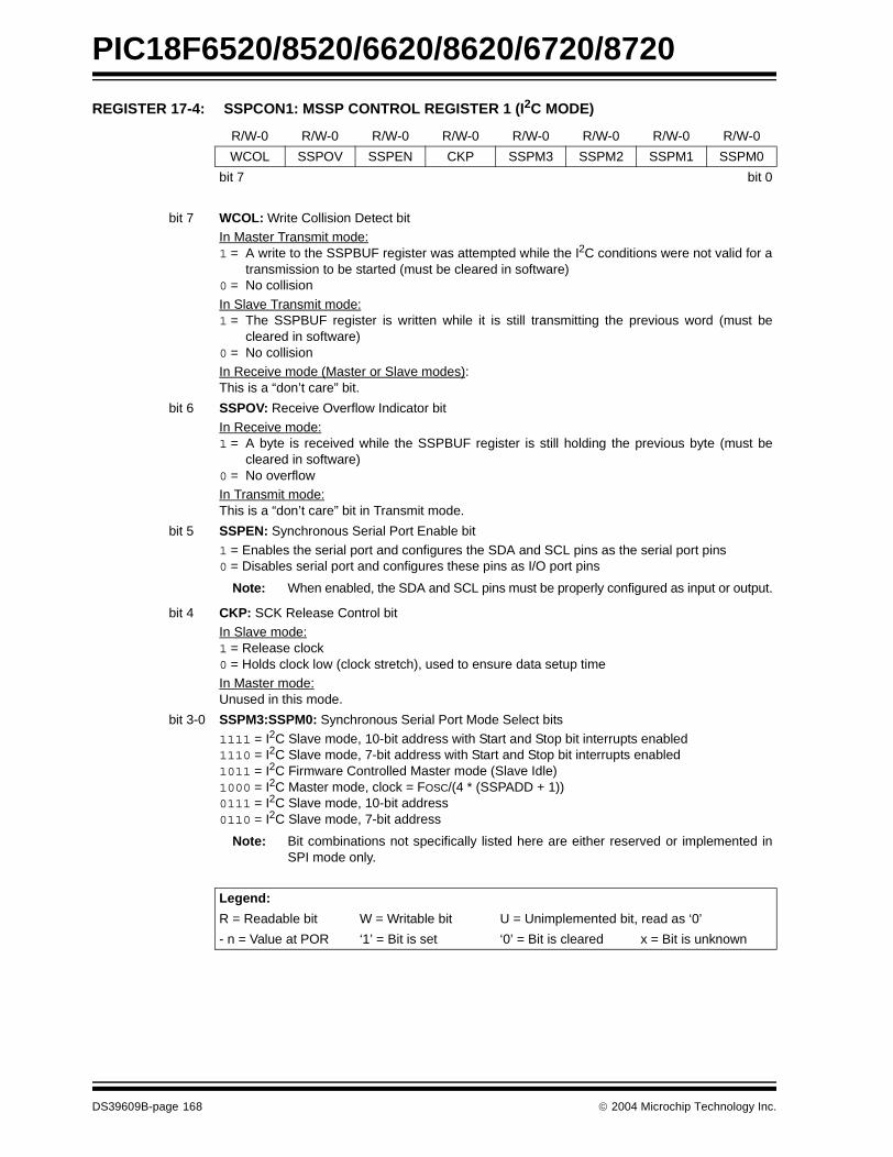
PIC18F6520/8520/6620/8620/6720/8720
REGISTER 17-4: SSPCON1: MSSP CONTROL REGISTER 1 (I2C MODE)
R/W-0 R/W-0 R/W-0 R/W-0 R/W-0 R/W-0 R/W-0 R/W-0
WCOL SSPOV SSPEN CKP SSPM3 SSPM2 SSPM1 SSPM0
bit 7 bit 0
bit 7 WCOL: Write Collision Detect bitIn Master Transmit mode: 1 = A write to the SSPBUF register was attempted while the I2C conditions were not valid for a
transmission to be started (must be cleared in software)0 = No collision
In Slave Transmit mode:1 = The SSPBUF register is written while it is still transmitting the previous word (must be
cleared in software) 0 = No collision In Receive mode (Master or Slave modes):This is a “don’t care” bit.
bit 6 SSPOV: Receive Overflow Indicator bit
In Receive mode: 1 = A byte is received while the SSPBUF register is still holding the previous byte (must be
cleared in software)0 = No overflowIn Transmit mode: This is a “don’t care” bit in Transmit mode.
bit 5 SSPEN: Synchronous Serial Port Enable bit
1 = Enables the serial port and configures the SDA and SCL pins as the serial port pins 0 = Disables serial port and configures these pins as I/O port pins
Note: When enabled, the SDA and SCL pins must be properly configured as input or output.
bit 4 CKP: SCK Release Control bit In Slave mode: 1 = Release clock 0 = Holds clock low (clock stretch), used to ensure data setup timeIn Master mode: Unused in this mode.
bit 3-0 SSPM3:SSPM0: Synchronous Serial Port Mode Select bits
1111 = I2C Slave mode, 10-bit address with Start and Stop bit interrupts enabled1110 = I2C Slave mode, 7-bit address with Start and Stop bit interrupts enabled1011 = I2C Firmware Controlled Master mode (Slave Idle)1000 = I2C Master mode, clock = FOSC/(4 * (SSPADD + 1)) 0111 = I2C Slave mode, 10-bit address0110 = I2C Slave mode, 7-bit address
Note: Bit combinations not specifically listed here are either reserved or implemented inSPI mode only.
Legend:
R = Readable bit W = Writable bit U = Unimplemented bit, read as ‘0’
- n = Value at POR ‘1’ = Bit is set ‘0’ = Bit is cleared x = Bit is unknown
DS39609B-page 168 2004 Microchip Technology Inc.

PIC18F6520/8520/6620/8620/6720/8720
REGISTER 17-5: SSPCON2: MSSP CONTROL REGISTER 2 (I2C MODE) R/W-0 R/W-0 R/W-0 R/W-0 R/W-0 R/W-0 R/W-0 R/W-0
GCEN ACKSTAT ACKDT ACKEN RCEN PEN RSEN SEN
bit 7 bit 0
bit 7 GCEN: General Call Enable bit (Slave mode only) 1 = Enable interrupt when a general call address (0000h) is received in the SSPSR 0 = General call address disabled
bit 6 ACKSTAT: Acknowledge Status bit (Master Transmit mode only)
1 = Acknowledge was not received from slave 0 = Acknowledge was received from slave
bit 5 ACKDT: Acknowledge Data bit (Master Receive mode only) 1 = Not Acknowledge 0 = Acknowledge
Note: Value that will be transmitted when the user initiates an Acknowledge sequence atthe end of a receive.
bit 4 ACKEN: Acknowledge Sequence Enable bit (Master Receive mode only)
1 = Initiate Acknowledge sequence on SDA and SCL pins and transmit ACKDT data bit.Automatically cleared by hardware.
0 = Acknowledge sequence Idle
bit 3 RCEN: Receive Enable bit (Master mode only) 1 = Enables Receive mode for I2C 0 = Receive Idle
bit 2 PEN: Stop Condition Enable bit (Master mode only)
1 = Initiate Stop condition on SDA and SCL pins. Automatically cleared by hardware. 0 = Stop condition Idle
bit 1 RSEN: Repeated Start Condition Enabled bit (Master mode only) 1 = Initiate Repeated Start condition on SDA and SCL pins. Automatically cleared by hardware.0 = Repeated Start condition Idle
bit 0 SEN: Start Condition Enabled/Stretch Enabled bitIn Master mode:1 = Initiate Start condition on SDA and SCL pins. Automatically cleared by hardware. 0 = Start condition Idle
In Slave mode:1 = Clock stretching is enabled for both Slave Transmit and Slave Receive (stretch enabled) 0 = Clock stretching is disabled
Note: For bits ACKEN, RCEN, PEN, RSEN, SEN: If the I2C module is not in the Idle mode,this bit may not be set (no spooling) and the SSPBUF may not be written (or writesto the SSPBUF are disabled).
Legend:
R = Readable bit W = Writable bit U = Unimplemented bit, read as ‘0’
- n = Value at POR ‘1’ = Bit is set ‘0’ = Bit is cleared x = Bit is unknown
2004 Microchip Technology Inc. DS39609B-page 169

PIC18F6520/8520/6620/8620/6720/8720
17.4.2 OPERATION
The MSSP module functions are enabled by settingMSSP Enable bit, SSPEN (SSPCON<5>).
The SSPCON1 register allows control of the I2C oper-ation. Four mode selection bits (SSPCON<3:0>) allowone of the following I2C modes to be selected:
• I2C Master mode, clock = (FOSC/4) x (SSPADD + 1)
• I2C Slave mode (7-bit address)• I2C Slave mode (10-bit address)• I2C Slave mode (7-bit address), with Start and
Stop bit interrupts enabled• I2C Slave mode (10-bit address), with Start and
Stop bit interrupts enabled• I2C Firmware Controlled Master mode, slave is
Idle
Selection of any I2C mode, with the SSPEN bit set,forces the SCL and SDA pins to be open-drain, pro-vided these pins are programmed to inputs by settingthe appropriate TRISC bits. To ensure proper operationof the module, pull-up resistors must be providedexternally to the SCL and SDA pins.
17.4.3 SLAVE MODE
In Slave mode, the SCL and SDA pins must be config-ured as inputs (TRISC<4:3> set). The MSSP modulewill override the input state with the output data whenrequired (slave-transmitter).
The I2C Slave mode hardware will always generate aninterrupt on an address match. Through the modeselect bits, the user can also choose to interrupt onStart and Stop bits
When an address is matched or the data transfer afteran address match is received, the hardware automati-cally will generate the Acknowledge (ACK) pulse andload the SSPBUF register with the received valuecurrently in the SSPSR register.
Any combination of the following conditions will causethe MSSP module not to give this ACK pulse:
• The Buffer Full bit BF (SSPSTAT<0>) was set before the transfer was received.
• The overflow bit SSPOV (SSPCON<6>) was set before the transfer was received.
In this case, the SSPSR register value is not loadedinto the SSPBUF, but bit SSPIF (PIR1<3>) is set. TheBF bit is cleared by reading the SSPBUF register, whilebit SSPOV is cleared through software.
The SCL clock input must have a minimum high andlow for proper operation. The high and low times of theI2C specification, as well as the requirement of theMSSP module, are shown in timing parameter #100and parameter #101.
17.4.3.1 Addressing
Once the MSSP module has been enabled, it waits fora Start condition to occur. Following the Start condition,the 8 bits are shifted into the SSPSR register. All incom-ing bits are sampled with the rising edge of the clock(SCL) line. The value of register SSPSR<7:1> iscompared to the value of the SSPADD register. Theaddress is compared on the falling edge of the eighthclock (SCL) pulse. If the addresses match and the BFand SSPOV bits are clear, the following events occur:
1. The SSPSR register value is loaded into theSSPBUF register.
2. The Buffer Full bit BF is set.3. An ACK pulse is generated.4. MSSP Interrupt Flag bit, SSPIF (PIR1<3>), is
set (interrupt is generated, if enabled) on thefalling edge of the ninth SCL pulse.
In 10-bit Address mode, two address bytes need to bereceived by the slave. The five Most Significant bits(MSbs) of the first address byte specify if this is a 10-bitaddress. Bit R/W (SSPSTAT<2>) must specify a writeso the slave device will receive the second addressbyte. For a 10-bit address, the first byte would equal‘11110 A9 A8 0’, where ‘A9’ and ‘A8’ are the twoMSbs of the address. The sequence of events for10-bit address is as follows, with steps 7 through 9 forthe slave-transmitter:
1. Receive first (high) byte of address (bits SSPIF,BF and bit UA (SSPSTAT<1>) are set).
2. Update the SSPADD register with second (low)byte of address (clears bit UA and releases theSCL line).
3. Read the SSPBUF register (clears bit BF) andclear flag bit SSPIF.
4. Receive second (low) byte of address (bitsSSPIF, BF and UA are set).
5. Update the SSPADD register with the first (high)byte of address. If match releases SCL line, thiswill clear bit UA.
6. Read the SSPBUF register (clears bit BF) andclear flag bit SSPIF.
7. Receive Repeated Start condition.8. Receive first (high) byte of address (bits SSPIF
and BF are set).9. Read the SSPBUF register (clears bit BF) and
clear flag bit SSPIF.
DS39609B-page 170 2004 Microchip Technology Inc.

PIC18F6520/8520/6620/8620/6720/8720
17.4.3.2 Reception
When the R/W bit of the address byte is clear and anaddress match occurs, the R/W bit of the SSPSTATregister is cleared. The received address is loaded intothe SSPBUF register and the SDA line is held low(ACK).
When the address byte overflow condition exists, thenthe no Acknowledge (ACK) pulse is given. An overflowcondition is defined as either bit BF (SSPSTAT<0>) isset, or bit SSPOV (SSPCON1<6>) is set.
An MSSP interrupt is generated for each data transferbyte. Flag bit SSPIF (PIR1<3>) must be cleared in soft-ware. The SSPSTAT register is used to determine thestatus of the byte.
If SEN is enabled (SSPCON1<0> = 1), RC3/SCK/SCLwill be held low (clock stretch) following each datatransfer. The clock must be released by setting bitCKP (SSPCON<4>). See Section 17.4.4 “ClockStretching” for more detail.
17.4.3.3 Transmission
When the R/W bit of the incoming address byte is setand an address match occurs, the R/W bit of theSSPSTAT register is set. The received address isloaded into the SSPBUF register. The ACK pulse willbe sent on the ninth bit and pin RC3/SCK/SCL is heldlow, regardless of SEN (see Section 17.4.4 “ClockStretching”, for more detail). By stretching the clock,the master will be unable to assert another clock pulseuntil the slave is done preparing the transmit data. Thetransmit data must be loaded into the SSPBUF register,which also loads the SSPSR register. Then pin RC3/SCK/SCL should be enabled by setting bit CKP(SSPCON1<4>). The eight data bits are shifted out onthe falling edge of the SCL input. This ensures that theSDA signal is valid during the SCL high time(Figure 17-9).
The ACK pulse from the master-receiver is latched onthe rising edge of the ninth SCL input pulse. If the SDAline is high (not ACK), then the data transfer iscomplete. In this case, when the ACK is latched by theslave, the slave logic is reset (resets SSPSTAT regis-ter) and the slave monitors for another occurrence ofthe Start bit. If the SDA line was low (ACK), the nexttransmit data must be loaded into the SSPBUF register.Again, pin RC3/SCK/SCL must be enabled by settingbit CKP.
An MSSP interrupt is generated for each data transferbyte. The SSPIF bit must be cleared in software andthe SSPSTAT register is used to determine the statusof the byte. The SSPIF bit is set on the falling edge ofthe ninth clock pulse.
2004 Microchip Technology Inc. DS39609B-page 171

PIC18F6520/8520/6620/8620/6720/8720
FIGURE 17-8: I2C SLAVE MODE TIMING WITH SEN = 0 (RECEPTION, 7-BIT ADDRESS)
SD
A
SC
L
SS
PIF
BF
(S
SP
STA
T<0
>)
SS
PO
V (
SS
PC
ON
<6>
)
S1
23
45
67
89
12
34
56
78
91
23
45
78
9P
A7
A6
A5
A4
A3
A2
A1
D7
D6
D5
D4
D3
D2
D1
D0
D7
D6
D5
D4
D3
D1
D0
AC
KR
ecei
ving
Dat
aA
CK
Rec
eivi
ng D
ata
R/W
= 0 A
CK
Rec
eivi
ng A
ddre
ss
Cle
ared
in s
oftw
are
SS
PB
UF
is r
ead
Bus
mas
ter
term
inat
estr
ansf
er
SS
PO
V is
set
beca
use
SS
PB
UF
isst
ill fu
ll. A
CK
is n
ot s
ent.
D2 6
(PIR
1<3>
)
CK
P(C
KP
doe
s no
t res
et to
‘0’ w
hen
SE
N =
0)
DS39609B-page 172 2004 Microchip Technology Inc.

PIC18F6520/8520/6620/8620/6720/8720
FIGURE 17-9: I2C SLAVE MODE TIMING (TRANSMISSION, 7-BIT ADDRESS)
SD
A
SC
L
SS
PIF
(P
IR1<
3>)
BF
(S
SP
STA
T<
0>)
A6
A5
A4
A3
A2
A1
D6
D5
D4
D3
D2
D1
D0
12
34
56
78
23
45
67
89
SS
PB
UF
is w
ritte
n in
sof
twar
e
Cle
ared
in s
oftw
are
SC
L he
ld lo
ww
hile
CP
Ure
spon
ds to
SS
PIF
Fro
m S
SP
IF IS
R
Dat
a in
sa
mpl
ed
S
AC
KTr
ansm
ittin
g D
ata
R/W
= 1
AC
K
Rec
eivi
ng A
ddre
ss
A7
D7
91
D6
D5
D4
D3
D2
D1
D0
23
45
67
89
SS
PB
UF
is w
ritte
n in
sof
twar
e
Cle
ared
in s
oftw
are
Fro
m S
SP
IF IS
R
Tran
smitt
ing
Dat
a
D7 1
CK
P
P
AC
K
CK
P is
set
in s
oftw
are
CK
P is
set
in s
oftw
are
2004 Microchip Technology Inc. DS39609B-page 173
PIC18F6520/8520/6620/8620/6720/8720
FIGURE 17-10: I2C SLAVE MODE TIMING WITH SEN = 0 (RECEPTION, 10-BIT ADDRESS)
SD
A
SC
L
SS
PIF
BF
(S
SP
STA
T<
0>)
S1
23
45
67
89
12
34
56
78
91
23
45
78
9P
11
11
0A
9A
8A
7A
6A
5A
4A
3A
2A
1A
0D
7D
6D
5D
4D
3D
1D
0
Rec
eive
Dat
a B
yte
AC
K
R/W
= 0 AC
K
Rec
eive
Firs
t Byt
e of
Add
ress
Cle
ared
in s
oftw
are
D2
6
(PIR
1<3>
)
Cle
ared
in s
oftw
are
Rec
eive
Sec
ond
Byt
e of
Add
ress
Cle
ared
by
hard
war
ew
hen
SS
PA
DD
is u
pdat
edw
ith lo
w b
yte
of a
ddre
ss
UA
(S
SP
STA
T<
1>)
Clo
ck is
hel
d lo
w u
ntil
upda
te o
f SS
PA
DD
has
ta
ken
plac
e
UA
is s
et in
dica
ting
that
the
SS
PA
DD
nee
ds to
be
upda
ted
UA
is s
et in
dica
ting
that
SS
PA
DD
nee
ds to
be
upda
ted
Cle
ared
by
hard
war
e w
hen
SS
PA
DD
is u
pdat
ed w
ith h
igh
byte
of a
ddre
ss
SS
PB
UF
is w
ritte
n w
ithco
nten
ts o
f SS
PS
RD
umm
y re
ad o
f SS
PB
UF
to c
lear
BF
flag
AC
K
CK
P
12
34
57
89
D7
D6
D5
D4
D3
D1
D0
Rec
eive
Dat
a B
yte
Bus
mas
ter
term
inat
estr
ansf
er
D2 6
AC
K
Cle
ared
in s
oftw
are
Cle
ared
in s
oftw
are
SS
PO
V (
SS
PC
ON
<6>
)
SS
PO
V is
set
beca
use
SS
PB
UF
isst
ill fu
ll. A
CK
is n
ot s
ent.
(CK
P d
oes
not r
eset
to ‘0
’ whe
n S
EN
= 0
)
Clo
ck is
hel
d lo
w u
ntil
upda
te o
f SS
PA
DD
has
ta
ken
plac
e
DS39609B-page 174 2004 Microchip Technology Inc.

PIC18F6520/8520/6620/8620/6720/8720
FIGURE 17-11: I2C SLAVE MODE TIMING (TRANSMISSION, 10-BIT ADDRESS)
SD
A
SC
L
SS
PIF
BF
(S
SP
STA
T<
0>)
S1
23
45
67
89
12
34
56
78
91
23
45
78
9P
11
11
0A
9A
8A
7A
6A
5A
4A
3A
2A
1A
01
11
10
A8
R/W
= 1 A
CK
AC
K
R/W
= 0
AC
K
Rec
eive
Firs
t Byt
e of
Add
ress
Cle
ared
in s
oftw
are
Bus
mas
ter
term
inat
estr
ansf
er
A9 6
(PIR
1<3>
)
Rec
eive
Sec
ond
Byt
e of
Add
ress
Cle
ared
by
hard
war
e w
hen
SS
PA
DD
is u
pdat
ed w
ith lo
wby
te o
f add
ress
UA
(S
SP
STA
T<
1>)
Clo
ck is
hel
d lo
w u
ntil
upda
te o
f SS
PA
DD
has
ta
ken
plac
e
UA
is s
et in
dica
ting
that
the
SS
PA
DD
nee
ds to
be
upda
ted
UA
is s
et in
dica
ting
that
SS
PA
DD
nee
ds to
be
upda
ted
Cle
ared
by
hard
war
e w
hen
SS
PA
DD
is u
pdat
ed w
ith h
igh
byte
of a
ddre
ss
SS
PB
UF
is w
ritte
n w
ithco
nten
ts o
f SS
PS
RD
umm
y re
ad o
f SS
PB
UF
to c
lear
BF
flag
Rec
eive
Firs
t Byt
e of
Add
ress
12
34
57
89
D7
D6
D5
D4
D3
D1
AC
K
D2
6
Tra
nsm
ittin
g D
ata
Byt
e
D0
Dum
my
read
of S
SP
BU
Fto
cle
ar B
F fl
ag
Sr
Cle
ared
in s
oftw
are
Writ
e of
SS
PB
UF
initi
ates
tran
smit
Cle
ared
in s
oftw
are
Com
plet
ion
of
clea
rs B
F fl
ag
CK
P (
SS
PC
ON
<4>
)
CK
P is
set
in s
oftw
are
CK
P is
aut
omat
ical
ly c
lear
ed in
har
dwar
e, h
oldi
ng S
CL
low
Clo
ck is
hel
d lo
w u
ntil
upda
te o
f SS
PA
DD
has
ta
ken
plac
e
data
tran
smis
sion
Clo
ck is
hel
d lo
w u
ntil
CK
P is
set
to ‘1
’
BF
flag
is c
lear
third
add
ress
seq
uenc
eat
the
end
of th
e
2004 Microchip Technology Inc. DS39609B-page 175

PIC18F6520/8520/6620/8620/6720/8720
17.4.4 CLOCK STRETCHING
Both 7- and 10-bit Slave modes implement automaticclock stretching during a transmit sequence.
The SEN bit (SSPCON2<0>) allows clock stretching tobe enabled during receives. Setting SEN will causethe SCL pin to be held low at the end of each datareceive sequence.
17.4.4.1 Clock Stretching for 7-bit Slave Receive Mode (SEN = 1)
In 7-bit Slave Receive mode, on the falling edge of theninth clock at the end of the ACK sequence, if the BFbit is set, the CKP bit in the SSPCON1 register isautomatically cleared, forcing the SCL output to beheld low. The CKP being cleared to ‘0’ will assert theSCL line low. The CKP bit must be set in the user’sISR before reception is allowed to continue. By holdingthe SCL line low, the user has time to service the ISRand read the contents of the SSPBUF before themaster device can initiate another receive sequence.This will prevent buffer overruns from occurring (seeFigure 17-13).
17.4.4.2 Clock Stretching for 10-bit Slave Receive Mode (SEN = 1)
In 10-bit Slave Receive mode, during the addresssequence, clock stretching automatically takes placebut CKP is not cleared. During this time, if the UA bit isset after the ninth clock, clock stretching is initiated.The UA bit is set after receiving the upper byte of the10-bit address and following the receive of the secondbyte of the 10-bit address with the R/W bit cleared to‘0’. The release of the clock line occurs upon updatingSSPADD. Clock stretching will occur on each datareceive sequence, as described in 7-bit mode.
17.4.4.3 Clock Stretching for 7-bit Slave Transmit Mode
7-bit Slave Transmit mode implements clock stretchingby clearing the CKP bit after the falling edge of theninth clock, if the BF bit is clear. This occurs,regardless of the state of the SEN bit.
The user’s ISR must set the CKP bit before transmis-sion is allowed to continue. By holding the SCL linelow, the user has time to service the ISR and load thecontents of the SSPBUF before the master device caninitiate another transmit sequence (see Figure 17-9).
17.4.4.4 Clock Stretching for 10-bit Slave Transmit Mode
In 10-bit Slave Transmit mode, clock stretching is con-trolled during the first two address sequences by thestate of the UA bit, just as it is in 10-bit Slave Receivemode. The first two addresses are followed by a thirdaddress sequence, which contains the high-order bitsof the 10-bit address and the R/W bit set to ‘1’. Afterthe third address sequence is performed, the UA bit isnot set, the module is now configured in Transmitmode and clock stretching is controlled as in 7-bitSlave Transmit mode (see Figure 17-11).
Note 1: If the user reads the contents of theSSPBUF before the falling edge of theninth clock, thus clearing the BF bit, theCKP bit will not be cleared and clockstretching will not occur.
2: The CKP bit can be set in software,regardless of the state of the BF bit. Theuser should be careful to clear the BF bitin the ISR before the next receivesequence, in order to prevent an overflowcondition.
Note: If the user polls the UA bit and clears it byupdating the SSPADD register before thefalling edge of the ninth clock occurs and ifthe user hasn’t cleared the BF bit by read-ing the SSPBUF register before that time,then the CKP bit will still NOT be assertedlow. Clock stretching on the basis of thestate of the BF bit only occurs during adata sequence, not an address sequence.
Note 1: If the user loads the contents of SSPBUF,setting the BF bit before the falling edge ofthe ninth clock, the CKP bit will not becleared and clock stretching will not occur.
2: The CKP bit can be set in software,regardless of the state of the BF bit.
DS39609B-page 176 2004 Microchip Technology Inc.

PIC18F6520/8520/6620/8620/6720/8720
17.4.4.5 Clock Synchronization and the CKP bit
When the CKP bit is cleared, the SCL output is forcedto ‘0’. However, clearing the CKP bit will not assert theSCL output low until the SCL output is already sam-pled low. Therefore, the CKP bit will not assert theSCL line until an external I2C master device has
already asserted the SCL line. The SCL output willremain low until the CKP bit is set and all otherdevices on the I2C bus have deasserted SCL. Thisensures that a write to the CKP bit will not violate theminimum high time requirement for SCL (seeFigure 17-12).
FIGURE 17-12: CLOCK SYNCHRONIZATION TIMING
SDA
SCL
DX-1DX
WR
Q1 Q2 Q3 Q4 Q1 Q2 Q3 Q4 Q1 Q2 Q3 Q4 Q1 Q2 Q3 Q4 Q1 Q2 Q3 Q4 Q1 Q2 Q3 Q4 Q1 Q2 Q3 Q4
SSPCON
CKP
Master devicedeasserts clock
Master deviceasserts clock
2004 Microchip Technology Inc. DS39609B-page 177

PIC18F6520/8520/6620/8620/6720/8720
FIGURE 17-13: I2C SLAVE MODE TIMING WITH SEN = 1 (RECEPTION, 7-BIT ADDRESS)
SD
A
SC
L
SS
PIF
BF
(S
SP
STA
T<
0>)
SS
PO
V (
SS
PC
ON
<6>
)
S1
23
45
67
89
12
34
56
78
91
23
45
78
9P
A7
A6
A5
A4
A3
A2
A1
D7
D6
D5
D4
D3
D2
D1
D0
D7
D6
D5
D4
D3
D1
D0
AC
KR
ecei
ving
Dat
aA
CK
Rec
eivi
ng D
ata
R/W
= 0 AC
K
Rec
eivi
ng A
ddre
ss
Cle
ared
in s
oftw
are
SS
PB
UF
is r
ead
Bus
mas
ter
term
inat
estr
ansf
er
SS
PO
V is
set
beca
use
SS
PB
UF
isst
ill fu
ll. A
CK
is n
ot s
ent.
D2 6
(PIR
1<3>
)
CK
P
CK
Pw
ritte
nto
‘1’ i
nIf
BF
is c
lear
edpr
ior
to th
e fa
lling
edge
of t
he 9
th c
lock
,C
KP
will
not
be
rese
tto
‘0’ a
nd n
o cl
ock
stre
tchi
ng w
ill o
ccur
softw
are
Clo
ck is
hel
d lo
w u
ntil
CK
P is
set
to ‘1
’
Clo
ck is
not
hel
d lo
wbe
caus
e bu
ffer
full
bit i
s cl
ear
prio
r to
falli
ng e
dge
of 9
th c
lock
C
lock
is n
ot h
eld
low
beca
use
AC
K =
1
BF
is s
et a
fter
falli
ng
edge
of t
he 9
th c
lock
,C
KP
is r
eset
to ‘0
’ and
cloc
k st
retc
hing
occ
urs
DS39609B-page 178 2004 Microchip Technology Inc.

PIC18F6520/8520/6620/8620/6720/8720
FIGURE 17-14: I2C SLAVE MODE TIMING SEN = 1 (RECEPTION, 10-BIT ADDRESS)
SD
A
SC
L
SS
PIF
BF
(S
SP
STA
T<
0>)
S1
23
45
67
89
12
34
56
78
91
23
45
78
9P
11
11
0A
9A
8A
7A
6A
5A
4A
3A
2A
1A
0D
7D
6D
5D
4D
3D
1D
0
Rec
eive
Dat
a B
yte
AC
K
R/W
= 0
AC
K
Rec
eive
Firs
t Byt
e of
Add
ress
Cle
ared
in s
oftw
are
D2
6
(PIR
1<3>
)
Cle
ared
in s
oftw
are
Rec
eive
Sec
ond
Byt
e of
Add
ress
Cle
ared
by
hard
war
e w
hen
SS
PA
DD
is u
pdat
ed w
ith lo
wby
te o
f add
ress
afte
r fa
lling
edg
e
UA
(S
SP
STA
T<
1>)
Clo
ck is
hel
d lo
w u
ntil
upda
te o
f SS
PA
DD
has
ta
ken
plac
e
UA
is s
et in
dica
ting
that
the
SS
PA
DD
nee
ds to
be
upda
ted
UA
is s
et in
dica
ting
that
SS
PA
DD
nee
ds to
be
upda
ted
Cle
ared
by
hard
war
e w
hen
SS
PA
DD
is u
pdat
ed w
ith h
igh
byte
of a
ddre
ss a
fter
falli
ng e
dge
SS
PB
UF
is w
ritte
n w
ithco
nten
ts o
f SS
PS
RD
umm
y re
ad o
f SS
PB
UF
to c
lear
BF
flag
AC
K
CK
P
12
34
57
89
D7
D6
D5
D4
D3
D1
D0
Rec
eive
Dat
a B
yte
Bus
mas
ter
term
inat
estr
ansf
er
D2 6
AC
K
Cle
ared
in s
oftw
are
Cle
ared
in s
oftw
are
SS
PO
V (
SS
PC
ON
<6>
)
CK
P w
ritte
n to
‘1’
No
te:
An
upda
te o
f the
SS
PA
DD
regi
ster
bef
ore
the
falli
nged
ge o
f the
nin
th c
lock
will
have
no
effe
ct o
n U
A a
ndU
A w
ill r
emai
n se
t
No
te:
An
upda
te o
f th
e S
SP
AD
Dre
gist
er b
efor
e th
e fa
lling
edge
of
the
nint
h cl
ock
will
have
no
effe
ct o
n U
A a
ndU
A w
ill r
emai
n se
tin
sof
twar
e
Clo
ck is
hel
d lo
w u
ntil
upda
te o
f SS
PA
DD
has
ta
ken
plac
e of n
inth
clo
ckof
nin
th c
lock
SS
PO
V is
set
beca
use
SS
PB
UF
isst
ill fu
ll. A
CK
is n
ot s
ent.
Dum
my
read
of S
SP
BU
Fto
cle
ar B
F fl
ag
Clo
ck is
hel
d lo
w u
ntil
CK
P is
set
to ‘1
’C
lock
is n
ot h
eld
low
beca
use
AC
K =
1
2004 Microchip Technology Inc. DS39609B-page 179

PIC18F6520/8520/6620/8620/6720/8720
17.4.5 GENERAL CALL ADDRESS SUPPORT
The addressing procedure for the I2C bus is such thatthe first byte after the Start condition usually deter-mines which device will be the slave addressed by themaster. The exception is the general call address,which can address all devices. When this address isused, all devices should, in theory, respond with anAcknowledge.
The general call address is one of eight addressesreserved for specific purposes by the I2C protocol. Itconsists of all ‘0’s with R/W = 0.
The general call address is recognized when the Gen-eral Call Enable bit (GCEN) is enabled (SSPCON2<7>set). Following a Start bit detect, 8 bits are shifted intothe SSPSR and the address is compared against theSSPADD. It is also compared to the general calladdress and fixed in hardware.
If the general call address matches, the SSPSR istransferred to the SSPBUF, the BF flag bit is set (eighthbit) and on the falling edge of the ninth bit (ACK bit), theSSPIF interrupt flag bit is set.
When the interrupt is serviced, the source for the inter-rupt can be checked by reading the contents of theSSPBUF. The value can be used to determine if theaddress was device specific or a general call address.
In 10-bit mode, the SSPADD is required to be updatedfor the second half of the address to match and the UAbit is set (SSPSTAT<1>). If the general call address issampled when the GCEN bit is set, while the slave isconfigured in 10-bit Address mode, then the secondhalf of the address is not necessary, the UA bit will notbe set and the slave will begin receiving data after theAcknowledge (Figure 17-15).
FIGURE 17-15: SLAVE MODE GENERAL CALL ADDRESS SEQUENCE (7 OR 10-BIT ADDRESS MODE)
SDA
SCL
S
SSPIF
BF (SSPSTAT<0>)
SSPOV (SSPCON1<6>)
Cleared in software
SSPBUF is read
R/W = 0ACKGeneral Call Address
Address is compared to General Call Address
GCEN (SSPCON2<7>)
Receiving Data ACK
1 2 3 4 5 6 7 8 9 1 2 3 4 5 6 7 8 9
D7 D6 D5 D4 D3 D2 D1 D0
after ACK, set interrupt
‘0’
‘1’
DS39609B-page 180 2004 Microchip Technology Inc.

PIC18F6520/8520/6620/8620/6720/8720
17.4.6 MASTER MODE
Master mode is enabled by setting and clearing theappropriate SSPM bits in SSPCON1 and by setting theSSPEN bit. In Master mode, the SCL and SDA linesare manipulated by the MSSP hardware.
Master mode of operation is supported by interruptgeneration on the detection of the Start and Stopconditions. The Stop (P) and Start (S) bits are clearedfrom a Reset, or when the MSSP module is disabled.Control of the I2C bus may be taken when the P bit isset or the bus is Idle, with both the S and P bits clear.
In Firmware Controlled Master mode, user codeconducts all I2C bus operations based on Start andStop bit conditions.
Once Master mode is enabled, the user has sixoptions.
1. Assert a Start condition on SDA and SCL.2. Assert a Repeated Start condition on SDA and
SCL.3. Write to the SSPBUF register initiating
transmission of data/address.4. Configure the I2C port to receive data.5. Generate an Acknowledge condition at the end
of a received byte of data.6. Generate a Stop condition on SDA and SCL.
The following events will cause SSP Interrupt Flag bit,SSPIF, to be set (SSP interrupt if enabled):
• Start Condition• Stop Condition
• Data Transfer Byte Transmitted/received• Acknowledge Transmit• Repeated Start
FIGURE 17-16: MSSP BLOCK DIAGRAM (I2C MASTER MODE)
Note: The MSSP module, when configured inI2C Master mode, does not allow queueingof events. For instance, the user is notallowed to initiate a Start condition andimmediately write the SSPBUF register toinitiate transmission before the Start condi-tion is complete. In this case, the SSPBUFwill not be written to and the WCOL bit willbe set, indicating that a write to theSSPBUF did not occur.
Read Write
SSPSR
Start bit, Stop bit,
Start bit Detect
SSPBUF
InternalData Bus
Set/Reset, S, P, WCOL (SSPSTAT)
ShiftClock
MSb LSb
SDA
AcknowledgeGenerate
Stop bit DetectWrite Collision Detect
Clock ArbitrationState Counter forend of XMIT/RCV
SCL
SCL In
Bus Collision
SDA In
Rec
eive
Ena
ble
Clo
ck C
ntl
Clo
ck A
rbitr
ate/
WC
OL
Det
ect
(hol
d of
f clo
ck s
ourc
e)
SSPADD<6:0>
Baud
Set SSPIF, BCLIFReset ACKSTAT, PEN (SSPCON2)
RateGenerator
SSPM3:SSPM0
2004 Microchip Technology Inc. DS39609B-page 181

PIC18F6520/8520/6620/8620/6720/8720
17.4.6.1 I2C Master Mode Operation
The master device generates all of the serial clockpulses and the Start and Stop conditions. A transfer isended with a Stop condition or with a Repeated Startcondition. Since the Repeated Start condition is alsothe beginning of the next serial transfer, the I2C bus willnot be released.
In Master Transmitter mode, serial data is outputthrough SDA, while SCL outputs the serial clock. Thefirst byte transmitted contains the slave address of thereceiving device (7 bits) and the Read/Write (R/W) bit.In this case, the R/W bit will be logic ‘0’. Serial data istransmitted 8 bits at a time. After each byte is transmit-ted, an Acknowledge bit is received. Start and Stopconditions are output to indicate the beginning and theend of a serial transfer.
In Master Receive mode, the first byte transmitted con-tains the slave address of the transmitting device(7 bits) and the R/W bit. In this case, the R/W bit will belogic ‘1’. Thus, the first byte transmitted is a 7-bit slaveaddress followed by a ‘1’ to indicate receive bit. Serialdata is received via SDA, while SCL outputs the serialclock. Serial data is received 8 bits at a time. After eachbyte is received, an Acknowledge bit is transmitted.Start and Stop conditions indicate the beginning andend of transmission.
The Baud Rate Generator used for the SPI modeoperation is used to set the SCL clock frequency foreither 100 kHz, 400 kHz or 1 MHz I2C operation. SeeSection 17.4.7 “Baud Rate Generator”, for moreinformation.
A typical transmit sequence would go as follows:
1. The user generates a Start condition by settingthe Start enable bit, SEN (SSPCON2<0>).
2. SSPIF is set. The MSSP module will wait therequired start time before any other operationtakes place.
3. The user loads the SSPBUF with the slaveaddress to transmit.
4. Address is shifted out the SDA pin until all 8 bitsare transmitted.
5. The MSSP module shifts in the ACK bit from theslave device and writes its value into theSSPCON2 register (SSPCON2<6>).
6. The MSSP module generates an interrupt at theend of the ninth clock cycle by setting the SSPIFbit.
7. The user loads the SSPBUF with eight bits ofdata.
8. Data is shifted out the SDA pin until all 8 bits aretransmitted.
9. The MSSP module shifts in the ACK bit from theslave device and writes its value into theSSPCON2 register (SSPCON2<6>).
10. The MSSP module generates an interrupt at theend of the ninth clock cycle by setting the SSPIFbit.
11. The user generates a Stop condition by settingthe Stop enable bit PEN (SSPCON2<2>).
12. Interrupt is generated once the Stop condition iscomplete.
DS39609B-page 182 2004 Microchip Technology Inc.

PIC18F6520/8520/6620/8620/6720/8720
17.4.7 BAUD RATE GENERATOR
In I2C Master mode, the Baud Rate Generator (BRG)reload value is placed in the lower 7 bits of theSSPADD register (Figure 17-17). When a write occursto SSPBUF, the Baud Rate Generator will automaticallybegin counting. The BRG counts down to ‘0’ and stopsuntil another reload has taken place. The BRG count isdecremented twice per instruction cycle (TCY) on theQ2 and Q4 clocks. In I2C Master mode, the BRG isreloaded automatically.
Once the given operation is complete (i.e., transmis-sion of the last data bit is followed by ACK), the internalclock will automatically stop counting and the SCL pinwill remain in its last state.
Table 15-3 demonstrates clock rates based oninstruction cycles and the BRG value loaded intoSSPADD.
FIGURE 17-17: BAUD RATE GENERATOR BLOCK DIAGRAM
TABLE 17-3: I2C CLOCK RATE W/BRG
SSPM3:SSPM0
BRG Down CounterCLKO FOSC/4
SSPADD<6:0>
SSPM3:SSPM0
SCL
Reload
Control
Reload
FCY FCY*2 BRG VALUEFSCL
(2 rollovers of BRG)
10 MHz 20 MHz 19h 400 kHz(1)
10 MHz 20 MHz 20h 312.5 kHz
10 MHz 20 MHz 3Fh 100 kHz
4 MHz 8 MHz 0Ah 400 kHz(1)
4 MHz 8 MHz 0Dh 308 kHz
4 MHz 8 MHz 28h 100 kHz
1 MHz 2 MHz 03h 333 kHz(1)
1 MHz 2 MHz 0Ah 100 kHz
1 MHz 2 MHz 00h 1 MHz(1)
Note 1: The I2C interface does not conform to the 400 kHz I2C specification (which applies to rates greater than 100 kHz) in all details, but may be used with care where higher rates are required by the application.
2004 Microchip Technology Inc. DS39609B-page 183

PIC18F6520/8520/6620/8620/6720/8720
17.4.7.1 Clock Arbitration
Clock arbitration occurs when the master, during anyreceive, transmit or Repeated Start/Stop condition,deasserts the SCL pin (SCL allowed to float high).When the SCL pin is allowed to float high, the BaudRate Generator (BRG) is suspended from countinguntil the SCL pin is actually sampled high. When the
SCL pin is sampled high, the Baud Rate Generator isreloaded with the contents of SSPADD<6:0> andbegins counting. This ensures that the SCL high timewill always be at least one BRG rollover count, in theevent that the clock is held low by an external device(Figure 15-18).
FIGURE 17-18: BAUD RATE GENERATOR TIMING WITH CLOCK ARBITRATION
SDA
SCL
SCL deasserted but slave holds
DX-1DX
BRG
SCL is sampled high, reload takesplace and BRG starts its count
03h 02h 01h 00h (hold off) 03h 02h
Reload
BRGValue
SCL low (clock arbitration)SCL allowed to transition high
BRG decrements onQ2 and Q4 cycles
DS39609B-page 184 2004 Microchip Technology Inc.

PIC18F6520/8520/6620/8620/6720/8720
17.4.8 I2C MASTER MODE START CONDITION TIMING
To initiate a Start condition, the user sets the Start Con-dition Enable bit, SEN (SSPCON2<0>). If the SDA andSCL pins are sampled high, the Baud Rate Generatoris reloaded with the contents of SSPADD<6:0> andstarts its count. If SCL and SDA are both sampled highwhen the Baud Rate Generator times out (TBRG), theSDA pin is driven low. The action of the SDA beingdriven low, while SCL is high, is the Start condition andcauses the S bit (SSPSTAT<3>) to be set. Followingthis, the Baud Rate Generator is reloaded with the con-tents of SSPADD<6:0> and resumes its count. Whenthe Baud Rate Generator times out (TBRG), the SEN bit(SSPCON2<0>) will be automatically cleared byhardware, the Baud Rate Generator is suspended,leaving the SDA line held low and the Start condition iscomplete.
17.4.8.1 WCOL Status Flag
If the user writes the SSPBUF when a Start sequenceis in progress, the WCOL is set and the contents of thebuffer are unchanged (the write doesn’t occur).
FIGURE 17-19: FIRST START BIT TIMING
Note: If at the beginning of the Start condition,the SDA and SCL pins are already sam-pled low, or if during the Start condition theSCL line is sampled low before the SDAline is driven low, a bus collision occurs,the Bus Collision Interrupt Flag, BCLIF, isset, the Start condition is aborted and theI2C module is reset into its Idle state.
Note: Because queueing of events is notallowed, writing to the lower 5 bits ofSSPCON2 is disabled until the Startcondition is complete.
SDA
SCL
S
TBRG
1st bit 2nd bit
TBRG
SDA = 1, At completion of Start bit,SCL = 1
Write to SSPBUF occurs hereTBRG
hardware clears SEN bit
TBRG
Write to SEN bit occurs hereSet S bit (SSPSTAT<3>)
and sets SSPIF bit
2004 Microchip Technology Inc. DS39609B-page 185

PIC18F6520/8520/6620/8620/6720/8720
17.4.9 I2C MASTER MODE REPEATED START CONDITION TIMING
A Repeated Start condition occurs when the RSEN bit(SSPCON2<1>) is programmed high and the I2C logicmodule is in the Idle state. When the RSEN bit is set,the SCL pin is asserted low. When the SCL pin is sam-pled low, the Baud Rate Generator is loaded with thecontents of SSPADD<5:0> and begins counting. TheSDA pin is released (brought high) for one Baud RateGenerator count (TBRG). When the Baud Rate Genera-tor times out, if SDA is sampled high, the SCL pin willbe deasserted (brought high). When SCL is sampledhigh, the Baud Rate Generator is reloaded with thecontents of SSPADD<6:0> and begins counting. SDAand SCL must be sampled high for one TBRG. Thisaction is then followed by assertion of the SDA pin(SDA = 0) for one TBRG, while SCL is high. Followingthis, the RSEN bit (SSPCON2<1>) will be automaticallycleared and the Baud Rate Generator will not bereloaded, leaving the SDA pin held low. As soon as aStart condition is detected on the SDA and SCL pins,the S bit (SSPSTAT<3>) will be set. The SSPIF bit willnot be set until the Baud Rate Generator has timed out.
Immediately following the setting of the SSPIF bit, theuser may write the SSPBUF with the 7-bit address in7-bit mode, or the default first address in 10-bit mode.After the first eight bits are transmitted and an ACK isreceived, the user may then transmit an additional eightbits of address (10-bit mode) or eight bits of data (7-bitmode).
17.4.9.1 WCOL Status Flag
If the user writes the SSPBUF when a Repeated Startsequence is in progress, the WCOL is set and thecontents of the buffer are unchanged (the write doesnot occur).
FIGURE 17-20: REPEAT START CONDITION WAVEFORM
Note 1: If RSEN is programmed while any otherevent is in progress, it will not take effect.
2: A bus collision during the Repeated Startcondition occurs if:
• SDA is sampled low when SCL goes from low-to-high.
• SCL goes low before SDA is asserted low. This may indicate that another master is attempting to transmit a data ‘1’.
Note: Because queueing of events is notallowed, writing of the lower 5 bits ofSSPCON2 is disabled until the RepeatedStart condition is complete.
SDA
SCL
Sr = Repeated Start
Write to SSPCON2
Write to SSPBUF occurs hereFalling edge of ninth clockEnd of Xmit
At completion of Start bit, hardware clears RSEN bit
1st bit
S bit set by hardware (SSPSTAT<3>)
TBRG
TBRG
SDA = 1,
SDA = 1,
SCL (no change).
SCL = 1occurs here.
TBRG TBRG TBRG
and sets SSPIF
RSEN bit set
DS39609B-page 186 2004 Microchip Technology Inc.

PIC18F6520/8520/6620/8620/6720/8720
17.4.10 I2C MASTER MODE TRANSMISSION
Transmission of a data byte, a 7-bit address, or theother half of a 10-bit address is accomplished by simplywriting a value to the SSPBUF register. This action willset the Buffer Full flag bit, BF and allow the Baud RateGenerator to begin counting and start the next trans-mission. Each bit of address/data will be shifted outonto the SDA pin after the falling edge of SCL isasserted (see data hold time specification parameter#106). SCL is held low for one Baud Rate Generatorrollover count (TBRG). Data should be valid before SCLis released high (see data setup time specificationparameter #107). When the SCL pin is released high, itis held that way for TBRG. The data on the SDA pinmust remain stable for that duration and some holdtime, after the next falling edge of SCL. After the eighthbit is shifted out (the falling edge of the eighth clock),the BF flag is cleared and the master releases SDA.This allows the slave device being addressed torespond with an ACK bit during the ninth bit time if anaddress match occurred, or if data was received prop-erly. The status of ACK is written into the ACKDT bit onthe falling edge of the ninth clock. If the master receivesan Acknowledge, the Acknowledge Status bit,ACKSTAT, is cleared. If not, the bit is set. After the ninthclock, the SSPIF bit is set and the master clock (BaudRate Generator) is suspended until the next data byteis loaded into the SSPBUF, leaving SCL low and SDAunchanged (Figure 17-21).
After the write to the SSPBUF, each address bit will beshifted out on the falling edge of SCL, until all sevenaddress bits and the R/W bit are completed. On the fall-ing edge of the eighth clock, the master will deassertthe SDA pin, allowing the slave to respond with anAcknowledge. On the falling edge of the ninth clock, themaster will sample the SDA pin to see if the addresswas recognized by a slave. The status of the ACK bit isloaded into the ACKSTAT status bit (SSPCON2<6>).Following the falling edge of the ninth clock transmis-sion of the address, the SSPIF is set, the BF flag iscleared and the Baud Rate Generator is turned off untilanother write to the SSPBUF takes place, holding SCLlow and allowing SDA to float.
17.4.10.1 BF Status Flag
In Transmit mode, the BF bit (SSPSTAT<0>) is setwhen the CPU writes to SSPBUF and is cleared whenall 8 bits are shifted out.
17.4.10.2 WCOL Status Flag
If the user writes the SSPBUF when a transmit isalready in progress (i.e., SSPSR is still shifting out adata byte), the WCOL is set and the contents of thebuffer are unchanged (the write doesn’t occur).
WCOL must be cleared in software.
17.4.10.3 ACKSTAT Status Flag
In Transmit mode, the ACKSTAT bit (SSPCON2<6>) iscleared when the slave has sent an Acknowledge(ACK = 0) and is set when the slave does not Acknowl-edge (ACK = 1). A slave sends an Acknowledge whenit has recognized its address (including a general call),or when the slave has properly received its data.
17.4.11 I2C MASTER MODE RECEPTION
Master mode reception is enabled by programming theReceive Enable bit, RCEN (SSPCON2<3>).
The Baud Rate Generator begins counting and on eachrollover, the state of the SCL pin changes (high-to-low/low-to-high) and data is shifted into the SSPSR. Afterthe falling edge of the eighth clock, the receive enableflag is automatically cleared, the contents of theSSPSR are loaded into the SSPBUF, the BF flag bit isset, the SSPIF flag bit is set and the Baud Rate Gener-ator is suspended from counting, holding SCL low. TheMSSP is now in Idle state, awaiting the next command.When the buffer is read by the CPU, the BF flag bit isautomatically cleared. The user can then send anAcknowledge bit at the end of reception by setting theAcknowledge Sequence Enable bit, ACKEN(SSPCON2<4>).
17.4.11.1 BF Status Flag
In receive operation, the BF bit is set when an addressor data byte is loaded into SSPBUF from SSPSR. It iscleared when the SSPBUF register is read.
17.4.11.2 SSPOV Status Flag
In receive operation, the SSPOV bit is set when 8 bitsare received into the SSPSR and the BF flag bit isalready set from a previous reception.
17.4.11.3 WCOL Status Flag
If the user writes the SSPBUF when a receive isalready in progress (i.e., SSPSR is still shifting in a databyte), the WCOL bit is set and the contents of the bufferare unchanged (the write doesn’t occur).
Note: The MSSP module must be in an Idle statebefore the RCEN bit is set, or the RCENbit will be disregarded.
2004 Microchip Technology Inc. DS39609B-page 187

PIC18F6520/8520/6620/8620/6720/8720
FIGURE 17-21: I2C MASTER MODE WAVEFORM (TRANSMISSION, 7 OR 10-BIT ADDRESS)
SD
A
SC
L
SS
PIF
BF
(S
SP
STA
T<
0>)
SE
N
A7
A6
A5
A4
A3
A2
A1
AC
K =
0D
7D
6D
5D
4D
3D
2D
1D
0
AC
KT
rans
mitt
ing
Dat
a or
Sec
ond
Hal
fR
/W =
0Tr
ansm
it A
ddre
ss to
Sla
ve
12
34
56
78
91
23
45
67
89
P
Cle
ared
in s
oftw
are
serv
ice
rout
ine
SS
PB
UF
is w
ritte
n in
sof
twar
e
from
SS
P in
terr
upt
Afte
r S
tart
con
ditio
n, S
EN
cle
ared
by
hard
war
e
S
SS
PB
UF
writ
ten
with
7-b
it ad
dres
s an
d R
/W,
star
t tra
nsm
it
SC
L he
ld lo
ww
hile
CP
Ure
spon
ds to
SS
PIF
SE
N =
0
of 1
0-bi
t Add
ress
Writ
e S
SP
CO
N2<
0> S
EN
= 1
,S
tart
con
ditio
n be
gins
Fro
m s
lave
, cle
ar A
CK
STA
T b
it S
SP
CO
N2<
6>
AC
KS
TAT
in
SS
PC
ON
2 =
1
Cle
ared
in s
oftw
are
SS
PB
UF
writ
ten
PE
N
Cle
ared
in s
oftw
are
R/W
DS39609B-page 188 2004 Microchip Technology Inc.
PIC18F6520/8520/6620/8620/6720/8720
FIGURE 17-22: I2C MASTER MODE WAVEFORM (RECEPTION, 7-BIT ADDRESS)
P9
87
65
D0
D1
D2
D3
D4
D5
D6
D7
S
A7
A6
A5
A4
A3
A2
A1
SD
A
SC
L1
23
45
67
89
12
34
56
78
91
23
4
Bus
mas
ter
term
inat
estr
ansf
er
AC
K
Rec
eivi
ng D
ata
from
Sla
veR
ecei
ving
Dat
a fr
om S
lave
D0
D1
D2
D3
D4
D5
D6
D7
AC
K
R/W
= 1
Tra
nsm
it A
ddre
ss to
Sla
ve
SS
PIF
BF
AC
K is
not
sen
t
Writ
e to
SS
PC
ON
2<0>
(SE
N =
1),
Writ
e to
SS
PB
UF
occ
urs
here
AC
K fr
om S
laveM
aste
r co
nfig
ured
as
a re
ceiv
erby
pro
gram
min
g S
SP
CO
N2<
3> (
RC
EN
= 1
)P
EN
bit
= 1
writ
ten
here
Dat
a sh
ifted
in o
n fa
lling
edg
e of
CLK
Cle
ared
in s
oftw
are
Sta
rt X
MIT
SE
N =
0
SS
PO
V
SD
A =
0, S
CL
= 1
whi
le C
PU
(SS
PS
TAT
<0>
)
AC
K
Last
bit
is s
hifte
d in
to S
SP
SR
and
cont
ents
are
unl
oade
d in
to S
SP
BU
F
Cle
ared
in s
oftw
are
Cle
ared
in s
oftw
are
Set
SS
PIF
inte
rrup
tat
end
of r
ecei
ve
Set
P b
it (S
SP
STA
T<
4>)
and
SS
PIF
Cle
ared
inso
ftwar
e
AC
K fr
om M
aste
r
Set
SS
PIF
at e
nd
Set
SS
PIF
inte
rrup
tat
end
of A
ckno
wle
dge
sequ
ence
Set
SS
PIF
inte
rrup
tat
end
of A
ckno
w-
ledg
e se
quen
ce
of r
ecei
ve
Set
AC
KE
N, s
tart
Ack
now
ledg
e se
quen
ce
SS
PO
V is
set
bec
ause
SS
PB
UF
is s
till f
ull
SD
A =
AC
KD
T =
1
RC
EN
cle
ared
auto
mat
ical
lyR
CE
N =
1
Sta
rt n
ext r
ecei
ve
Writ
e to
SS
PC
ON
2<4>
to s
tart
Ack
now
ledg
e se
quen
ceS
DA
= A
CK
DT
(S
SP
CO
N2<
5>)
= 0
RC
EN
cle
ared
auto
mat
ical
ly
resp
onds
to S
SP
IF
AC
KE
Nbegi
n S
tart
Con
ditio
n
Cle
ared
in s
oftw
are
SD
A =
AC
KD
T =
0
2004 Microchip Technology Inc. DS39609B-page 189

PIC18F6520/8520/6620/8620/6720/8720
17.4.12 ACKNOWLEDGE SEQUENCE TIMING
An Acknowledge sequence is enabled by setting theAcknowledge Sequence Enable bit, ACKEN(SSPCON2<4>). When this bit is set, the SCL pin ispulled low and the contents of the Acknowledge data bitare presented on the SDA pin. If the user wishes to gen-erate an Acknowledge, then the ACKDT bit should becleared. If not, the user should set the ACKDT bit beforestarting an Acknowledge sequence. The Baud RateGenerator then counts for one rollover period (TBRG)and the SCL pin is deasserted (pulled high). When theSCL pin is sampled high (clock arbitration), the BaudRate Generator counts for TBRG. The SCL pin is thenpulled low. Following this, the ACKEN bit is automaticallycleared, the Baud Rate Generator is turned off and theMSSP module then goes into Idle mode (Figure 17-23).
17.4.12.1 WCOL Status Flag
If the user writes the SSPBUF when an Acknowledgesequence is in progress, then WCOL is set and thecontents of the buffer are unchanged (the write doesn’toccur).
17.4.13 STOP CONDITION TIMING
A Stop bit is asserted on the SDA pin at the end of areceive/transmit by setting the Stop Sequence Enablebit, PEN (SSPCON2<2>). At the end of a receive/transmit, the SCL line is held low after the falling edgeof the ninth clock. When the PEN bit is set, the masterwill assert the SDA line low. When the SDA line is sam-pled low, the Baud Rate Generator is reloaded andcounts down to ‘0’. When the Baud Rate Generatortimes out, the SCL pin will be brought high and oneTBRG (Baud Rate Generator rollover count) later, theSDA pin will be deasserted. When the SDA pin is sam-pled high while SCL is high, the P bit (SSPSTAT<4>) isset. A TBRG later, the PEN bit is cleared and the SSPIFbit is set (Figure 17-24).
17.4.13.1 WCOL Status Flag
If the user writes the SSPBUF when a Stop sequenceis in progress, then the WCOL bit is set and thecontents of the buffer are unchanged (the write doesn’toccur).
FIGURE 17-23: ACKNOWLEDGE SEQUENCE WAVEFORM
FIGURE 17-24: STOP CONDITION RECEIVE OR TRANSMIT MODE
SDA
SCL
SSPIF set at the end
Acknowledge sequence starts here,Write to SSPCON2
ACKEN automatically cleared
Cleared in
TBRG TBRG
of receive
8
ACKEN = 1, ACKDT = 0
D0
9
SSPIF
software SSPIF set at the endof Acknowledge sequence
Cleared insoftware
Note: TBRG = one Baud Rate Generator period.
ACK
SCL
SDA
SDA asserted low before rising edge of clock
Write to SSPCON2Set PEN
Falling edge of
SCL = 1 for TBRG, followed by SDA = 1 for TBRG
9th clock
SCL brought high after TBRG
Note: TBRG = one Baud Rate Generator period.
TBRG TBRG
after SDA sampled high. P bit (SSPSTAT<4>) is set.
TBRG
to setup Stop condition
ACK
PTBRG
PEN bit (SSPCON2<2>) is cleared by hardware and the SSPIF bit is set
DS39609B-page 190 2004 Microchip Technology Inc.

PIC18F6520/8520/6620/8620/6720/8720
17.4.14 SLEEP OPERATION
While in Sleep mode, the I2C module can receiveaddresses or data and when an address match orcomplete byte transfer occurs, wake the processorfrom Sleep (if the MSSP interrupt is enabled).
17.4.15 EFFECT OF A RESET
A Reset disables the MSSP module and terminates thecurrent transfer.
17.4.16 MULTI-MASTER MODE
In Multi-Master mode, the interrupt generation on thedetection of the Start and Stop conditions allows thedetermination of when the bus is free. The Stop (P) andStart (S) bits are cleared from a Reset or when theMSSP module is disabled. Control of the I2C bus maybe taken when the P bit (SSPSTAT<4>) is set, or thebus is idle with both the S and P bits clear. When thebus is busy, enabling the SSP interrupt will generatethe interrupt when the Stop condition occurs.
In multi-master operation, the SDA line must be moni-tored for arbitration, to see if the signal level is theexpected output level. This check is performed inhardware, with the result placed in the BCLIF bit.
The states where arbitration can be lost are:
• Address Transfer
• Data Transfer• A Start Condition • A Repeated Start Condition
• An Acknowledge Condition
17.4.17 MULTI -MASTER COMMUNICATION, BUS COLLISION AND BUS ARBITRATION
Multi-Master mode support is achieved by bus arbitra-tion. When the master outputs address/data bits ontothe SDA pin, arbitration takes place when the masteroutputs a ‘1’ on SDA, by letting SDA float high andanother master asserts a ‘0’. When the SCL pin floatshigh, data should be stable. If the expected data onSDA is a ‘1’ and the data sampled on the SDA pin = 0,then a bus collision has taken place. The master will setthe Bus Collision Interrupt Flag, BCLIF and reset theI2C port to its Idle state (Figure 17-25).
If a transmit was in progress when the bus collisionoccurred, the transmission is halted, the BF flag iscleared, the SDA and SCL lines are deasserted and theSSPBUF can be written to. When the user services thebus collision Interrupt Service Routine and if the I2Cbus is free, the user can resume communication byasserting a Start condition.
If a Start, Repeated Start, Stop, or Acknowledge condi-tion was in progress when the bus collision occurred,the condition is aborted, the SDA and SCL lines aredeasserted and the respective control bits in theSSPCON2 register are cleared. When the user ser-vices the bus collision Interrupt Service Routine and ifthe I2C bus is free, the user can resume communicationby asserting a Start condition.
The master will continue to monitor the SDA and SCLpins. If a Stop condition occurs, the SSPIF bit will be set.
A write to the SSPBUF will start the transmission ofdata at the first data bit, regardless of where thetransmitter left off when the bus collision occurred.
In Multi-Master mode, the interrupt generation on thedetection of Start and Stop conditions allows the determi-nation of when the bus is free. Control of the I2C bus canbe taken when the P bit is set in the SSPSTAT register, orthe bus is Idle and the S and P bits are cleared.
FIGURE 17-25: BUS COLLISION TIMING FOR TRANSMIT AND ACKNOWLEDGE
SDA
SCL
BCLIF
SDA released
SDA line pulled lowby another source
Sample SDA. While SCL is high,data doesn’t match what is driven
Bus collision has occurred.
Set bus collisioninterrupt (BCLIF)
by the master.
by master
Data changeswhile SCL = 0
2004 Microchip Technology Inc. DS39609B-page 191

PIC18F6520/8520/6620/8620/6720/8720
17.4.17.1 Bus Collision During a Start Condition
During a Start condition, a bus collision occurs if:
a) SDA or SCL are sampled low at the beginning ofthe Start condition (Figure 17-26).
b) SCL is sampled low before SDA is asserted low(Figure 17-27).
During a Start condition, both the SDA and the SCLpins are monitored.
If the SDA pin is already low, or the SCL pin is alreadylow, then all of the following occur:
• the Start condition is aborted, • the BCLIF flag is set and• the MSSP module is reset to its Idle state
(Figure 17-26).
The Start condition begins with the SDA and SCL pinsdeasserted. When the SDA pin is sampled high, theBaud Rate Generator is loaded from SSPADD<6:0>and counts down to ‘0’. If the SCL pin is sampled lowwhile SDA is high, a bus collision occurs, because it isassumed that another master is attempting to drive adata ‘1’ during the Start condition.
If the SDA pin is sampled low during this count, theBRG is reset and the SDA line is asserted early(Figure 17-28). If, however, a ‘1’ is sampled on the SDApin, the SDA pin is asserted low at the end of the BRGcount. The Baud Rate Generator is then reloaded andcounts down to ‘0’ and during this time, if the SCL pinis sampled as ‘0’, a bus collision does not occur. At theend of the BRG count, the SCL pin is asserted low.
FIGURE 17-26: BUS COLLISION DURING START CONDITION (SDA ONLY)
Note: The reason that bus collision is not a factorduring a Start condition is that no two busmasters can assert a Start condition at theexact same time. Therefore, one masterwill always assert SDA before the other.This condition does not cause a bus colli-sion because the two masters must beallowed to arbitrate the first address fol-lowing the Start condition. If the address isthe same, arbitration must be allowed tocontinue into the data portion, RepeatedStart or Stop conditions.
SDA
SCL
SEN
SDA sampled low before
SDA goes low before the SEN bit is set.
S bit and SSPIF set because
SSP module reset into Idle state.SEN cleared automatically because of bus collision.
S bit and SSPIF set because
Set SEN, enable Startcondition if SDA = 1, SCL = 1
SDA = 0, SCL = 1.
BCLIF
S
SSPIF
SDA = 0, SCL = 1.
SSPIF and BCLIF arecleared in software
SSPIF and BCLIF arecleared in software
Set BCLIF,
Start condition. Set BCLIF.
DS39609B-page 192 2004 Microchip Technology Inc.

PIC18F6520/8520/6620/8620/6720/8720
FIGURE 17-27: BUS COLLISION DURING START CONDITION (SCL = 0)
FIGURE 17-28: BRG RESET DUE TO SDA ARBITRATION DURING START CONDITION
SDA
SCL
SENbus collision occurs. Set BCLIF.SCL = 0 before SDA = 0,
Set SEN, enable Startsequence if SDA = 1, SCL = 1
TBRG TBRG
SDA = 0, SCL = 1
BCLIF
S
SSPIF
Interrupt clearedin software
bus collision occurs. Set BCLIF.SCL = 0 before BRG time-out,
‘0’ ‘0’
‘0’‘0’
SDA
SCL
SEN
Set S
Set SEN, enable Startsequence if SDA = 1, SCL = 1
Less than TBRGTBRG
SDA = 0, SCL = 1
BCLIF
S
SSPIF
S
Interrupts clearedin softwareSet SSPIF
SDA = 0, SCL = 1
SCL pulled low after BRGTime-out
Set SSPIF
‘0’
SDA pulled low by other master.Reset BRG and assert SDA.
2004 Microchip Technology Inc. DS39609B-page 193

PIC18F6520/8520/6620/8620/6720/8720
17.4.17.2 Bus Collision During a Repeated Start Condition
During a Repeated Start condition, a bus collisionoccurs if:
a) A low level is sampled on SDA when SCL goesfrom low level to high level.
b) SCL goes low before SDA is asserted low,indicating that another master is attempting totransmit a data ‘1’.
When the user deasserts SDA and the pin is allowed tofloat high, the BRG is loaded with SSPADD<6:0> andcounts down to ‘0’. The SCL pin is then deasserted andwhen sampled high, the SDA pin is sampled.
If SDA is low, a bus collision has occurred (i.e., anothermaster is attempting to transmit a data ‘0’, Figure 17-29).If SDA is sampled high, the BRG is reloaded and beginscounting. If SDA goes from high-to-low before the BRGtimes out, no bus collision occurs because no twomasters can assert SDA at exactly the same time.
If SCL goes from high-to-low before the BRG times outand SDA has not already been asserted, a bus collisionoccurs. In this case, another master is attempting totransmit a data ‘1’ during the Repeated Start condition,Figure 17-30.
If, at the end of the BRG time-out, both SCL and SDAare still high, the SDA pin is driven low and the BRG isreloaded and begins counting. At the end of the count,regardless of the status of the SCL pin, the SCL pin isdriven low and the Repeated Start condition is complete.
FIGURE 17-29: BUS COLLISION DURING A REPEATED START CONDITION (CASE 1)
FIGURE 17-30: BUS COLLISION DURING REPEATED START CONDITION (CASE 2)
SDA
SCL
RSEN
BCLIF
S
SSPIF
Sample SDA when SCL goes high.If SDA = 0, set BCLIF and release SDA and SCL.
Cleared in software
‘0’
‘0’
SDA
SCL
BCLIF
RSEN
S
SSPIF
Interrupt clearedin software
SCL goes low before SDA,Set BCLIF. Release SDA and SCL.
TBRG TBRG
‘0’
DS39609B-page 194 2004 Microchip Technology Inc.
PIC18F6520/8520/6620/8620/6720/8720
17.4.17.3 Bus Collision During a Stop Condition
Bus collision occurs during a Stop condition if:
a) After the SDA pin has been deasserted andallowed to float high, SDA is sampled low afterthe BRG has timed out.
b) After the SCL pin is deasserted, SCL is sampledlow before SDA goes high.
The Stop condition begins with SDA asserted low.When SDA is sampled low, the SCL pin is allowed tofloat. When the pin is sampled high (clock arbitration),the Baud Rate Generator is loaded with SSPADD<6:0>and counts down to ‘0’. After the BRG times out, SDAis sampled. If SDA is sampled low, a bus collision hasoccurred. This is due to another master attempting todrive a data ‘0’ (Figure 17-31). If the SCL pin issampled low before SDA is allowed to float high, a buscollision occurs. This is another case of another masterattempting to drive a data ‘0’ (Figure 17-32).
FIGURE 17-31: BUS COLLISION DURING A STOP CONDITION (CASE 1)
FIGURE 17-32: BUS COLLISION DURING A STOP CONDITION (CASE 2)
SDA
SCL
BCLIF
PEN
P
SSPIF
TBRG TBRG TBRG
SDA asserted low
SDA sampledlow after TBRG,set BCLIF
‘0’
‘0’
SDA
SCL
BCLIF
PEN
P
SSPIF
TBRG TBRG TBRG
Assert SDA SCL goes low before SDA goes high,set BCLIF
‘0’
‘0’
2004 Microchip Technology Inc. DS39609B-page 195

PIC18F6520/8520/6620/8620/6720/8720
NOTES:
DS39609B-page 196 2004 Microchip Technology Inc.

PIC18F6520/8520/6620/8620/6720/8720
18.0 ADDRESSABLE UNIVERSAL SYNCHRONOUS ASYNCHRONOUS RECEIVER TRANSMITTER (USART)
The Universal Synchronous Asynchronous ReceiverTransmitter (USART) module (also known as a SerialCommunications Interface or SCI) is one of the twotypes of serial I/O modules available on PIC18FXX20devices. Each device has two USARTs, which can beconfigured independently of each other. Each can beconfigured as a full-duplex asynchronous system thatcan communicate with peripheral devices, such asCRT terminals and personal computers, or as a half-duplex synchronous system that can communicatewith peripheral devices, such as A/D or D/A integratedcircuits, serial EEPROMs, etc.
The USART can be configured in the following modes:
• Asynchronous (full-duplex)• Synchronous – Master (half-duplex)
• Synchronous – Slave (half-duplex)
The pins of USART1 and USART2 are multiplexed withthe functions of PORTC (RC6/TX1/CK1 and RC7/RX1/DT1) and PORTG (RG1/TX2/CK2 and RG2/RX2/DT2),respectively. In order to configure these pins as aUSART:
• For USART1:
- bit SPEN (RCSTA1<7>) must be set (= 1)- bit TRISC<7> must be set (= 1)- bit TRISC<6> must be cleared (= 0) for
Asynchronous and Synchronous Master modes
- bit TRISC<6> must be set (= 1) for Synchronous Slave mode
• For USART2:- bit SPEN (RCSTA2<7>) must be set (= 1)
- bit TRISG<2> must be set (= 1)- bit TRISG<1> must be cleared (= 0) for
Asynchronous and Synchronous Master modes
- bit TRISC<6> must be set (= 1) for Synchronous Slave mode
Register 18-1 shows the layout of the Transmit Statusand Control registers (TXSTAx) and Register 18-2shows the layout of the Receive Status and Controlregisters (RCSTAx). USART1 and USART2 each havetheir own independent and distinct pairs of transmit andreceive control registers, which are identical to eachother apart from their names. Similarly, each USARThas its own distinct set of transmit, receive and baudrate registers.
Note: Throughout this section, references toregister and bit names that may be associ-ated with a specific USART module arereferred to generically by the use of ‘x’ inplace of the specific module number.Thus, “RCSTAx” might refer to the receivestatus register for either USART1 orUSART2.
2004 Microchip Technology Inc. DS39609B-page 197

PIC18F6520/8520/6620/8620/6720/8720
REGISTER 18-1: TXSTAx: TRANSMIT STATUS AND CONTROL REGISTER R/W-0 R/W-0 R/W-0 R/W-0 U-0 R/W-0 R-1 R/W-0CSRC TX9 TXEN SYNC — BRGH TRMT TX9D
bit 7 bit 0
bit 7 CSRC: Clock Source Select bitAsynchronous mode: Don’t care.Synchronous mode: 1 = Master mode (clock generated internally from BRG) 0 = Slave mode (clock from external source)
bit 6 TX9: 9-bit Transmit Enable bit 1 = Selects 9-bit transmission 0 = Selects 8-bit transmission
bit 5 TXEN: Transmit Enable bit 1 = Transmit enabled 0 = Transmit disabled
Note: SREN/CREN overrides TXEN in Sync mode.
bit 4 SYNC: USART Mode Select bit
1 = Synchronous mode 0 = Asynchronous mode
bit 3 Unimplemented: Read as ‘0’
bit 2 BRGH: High Baud Rate Select bit Asynchronous mode: 1 = High speed 0 = Low speed
Synchronous mode: Unused in this mode.
bit 1 TRMT: Transmit Shift Register Status bit 1 = TSR empty 0 = TSR full
bit 0 TX9D: 9th bit of Transmit DataCan be address/data bit or a parity bit.
Legend:
R = Readable bit W = Writable bit U = Unimplemented bit, read as ‘0’
- n = Value at POR ‘1’ = Bit is set ‘0’ = Bit is cleared x = Bit is unknown
DS39609B-page 198 2004 Microchip Technology Inc.

PIC18F6520/8520/6620/8620/6720/8720
REGISTER 18-2: RCSTAx: RECEIVE STATUS AND CONTROL REGISTER R/W-0 R/W-0 R/W-0 R/W-0 R/W-0 R-0 R-0 R-xSPEN RX9 SREN CREN ADDEN FERR OERR RX9D
bit 7 bit 0
bit 7 SPEN: Serial Port Enable bit 1 = Serial port enabled (configures RX/DT and TX/CK pins as serial port pins) 0 = Serial port disabled
bit 6 RX9: 9-bit Receive Enable bit
1 = Selects 9-bit reception 0 = Selects 8-bit reception
bit 5 SREN: Single Receive Enable bit Asynchronous mode: Don’t care.Synchronous mode – Master: 1 = Enables single receive0 = Disables single receive This bit is cleared after reception is complete.
Synchronous mode – Slave: Don’t care.
bit 4 CREN: Continuous Receive Enable bit Asynchronous mode: 1 = Enables receiver 0 = Disables receiverSynchronous mode: 1 = Enables continuous receive until enable bit CREN is cleared (CREN overrides SREN) 0 = Disables continuous receive
bit 3 ADDEN: Address Detect Enable bitAsynchronous mode 9-bit (RX9 = 1):1 = Enables address detection, enables interrupt and load of the receive buffer when RSR<8>
is set0 = Disables address detection, all bytes are received and ninth bit can be used as parity bit
bit 2 FERR: Framing Error bit 1 = Framing error (can be updated by reading RCREG register and receive next valid byte) 0 = No framing error
bit 1 OERR: Overrun Error bit 1 = Overrun error (can be cleared by clearing bit CREN) 0 = No overrun error
bit 0 RX9D: 9th bit of Received Data
This can be address/data bit or a parity bit and must be calculated by user firmware.
Legend:
R = Readable bit W = Writable bit U = Unimplemented bit, read as ‘0’
- n = Value at POR ‘1’ = Bit is set ‘0’ = Bit is cleared x = Bit is unknown
2004 Microchip Technology Inc. DS39609B-page 199

PIC18F6520/8520/6620/8620/6720/8720
18.1 USART Baud Rate Generator (BRG)
The BRG supports both the Asynchronous andSynchronous modes of the USARTs. It is a dedicated8-bit Baud Rate Generator. The SPBRG registercontrols the period of a free running 8-bit timer. In Asyn-chronous mode, bit BRGH (TXSTAx<2>) also controlsthe baud rate. In Synchronous mode, bit BRGH isignored. Table 18-1 shows the formula for computationof the baud rate for different USART modes, which onlyapply in Master mode (internal clock).
Given the desired baud rate and FOSC, the nearestinteger value for the SPBRGx register can be calcu-lated using the formula in Table 18-1. From this, theerror in baud rate can be determined.
Example 18-1 shows the calculation of the baud rateerror for the following conditions:
• FOSC = 16 MHz• Desired Baud Rate = 9600• BRGH = 0
• SYNC = 0
It may be advantageous to use the high baud rate(BRGH = 1) even for slower baud clocks. This isbecause the equation in Example 18-1 can reduce thebaud rate error in some cases.
Writing a new value to the SPBRGx register causes theBRG timer to be reset (or cleared). This ensures theBRG does not wait for a timer overflow beforeoutputting the new baud rate.
18.1.1 SAMPLING
The data on the RXx pin (either RC7/RX1/DT1 or RG2/RX2/DT2) is sampled three times by a majority detectcircuit to determine if a high or a low level is present atthe pin.
EXAMPLE 18-1: CALCULATING BAUD RATE ERROR
TABLE 18-1: BAUD RATE FORMULA
TABLE 18-2: REGISTERS ASSOCIATED WITH BAUD RATE GENERATOR
SYNC BRGH = 0 (Low Speed) BRGH = 1 (High Speed)
01
(Asynchronous) Baud Rate = FOSC/(64(X + 1))(Synchronous) Baud Rate = FOSC/(4(X + 1))
Baud Rate = FOSC/(16(X + 1))N/A
Legend: X = value in SPBRGx (0 to 255)
Name Bit 7 Bit 6 Bit 5 Bit 4 Bit 3 Bit 2 Bit 1 Bit 0Value on
POR, BOR
Value on all other Resets
TXSTAx CSRC TX9 TXEN SYNC — BRGH TRMT TX9D 0000 -010 0000 -010
RCSTAx SPEN RX9 SREN CREN ADDEN FERR OERR RX9D 0000 000x 0000 000x
SPBRGx Baud Rate Generator Register 0000 0000 0000 0000
Legend: x = unknown, – = unimplemented, read as ‘0’. Shaded cells are not used by the BRG.Note 1: Register names generically refer to both of the identically named registers for the two USART modules,
where ‘x’ indicates the particular module. Bit names and Reset values are identical between modules.
Desired Baud Rate = FOSC/(64 (X + 1))
Solving for X:
X = ((FOSC/Desired Baud Rate)/64 ) – 1X = ((16000000/9600)/64) – 1 X = [25.042] = 25
Calculated Baud Rate = 16000000/(64 (25 + 1)) = 9615
Error = (Calculated Baud Rate – Desired Baud Rate) Desired Baud Rate = (9615 – 9600)/9600 = 0.16%
DS39609B-page 200 2004 Microchip Technology Inc.

PIC18F6520/8520/6620/8620/6720/8720
TABLE 18-3: BAUD RATES FOR SYNCHRONOUS MODE
BAUDRATE(Kbps)
FOSC = 40 MHz 33 MHz 25 MHz 20 MHz
KBAUD%
ERROR
SPBRGvalue
(decimal) KBAUD%
ERROR
SPBRGvalue
(decimal) KBAUD%
ERROR
SPBRGvalue
(decimal) KBAUD%
ERROR
SPBRGvalue
(decimal)
0.3 NA - - NA - - NA - - NA - -
1.2 NA - - NA - - NA - - NA - -
2.4 NA - - NA - - NA - - NA - -
9.6 NA - - NA - - NA - - NA - -
19.2 NA - - NA - - NA - - NA - -
76.8 76.92 +0.16 129 77.10 +0.39 106 77.16 +0.47 80 76.92 +0.16 64
96 96.15 +0.16 103 95.93 -0.07 85 96.15 +0.16 64 96.15 +0.16 51
300 303.03 +1.01 32 294.64 -1.79 27 297.62 -0.79 20 294.12 -1.96 16
500 500 0 19 485.30 -2.94 16 480.77 -3.85 12 500 0 9
HIGH 10000 - 0 8250 - 0 6250 - 0 5000 - 0
LOW 39.06 - 255 32.23 - 255 24.41 - 255 19.53 - 255
BAUDRATE(Kbps)
FOSC = 16 MHz 10 MHz 7.15909 MHz 5.0688 MHz
KBAUD%
ERROR
SPBRGvalue
(decimal) KBAUD%
ERROR
SPBRGvalue
(decimal) KBAUD%
ERROR
SPBRGvalue
(decimal) KBAUD%
ERROR
SPBRGvalue
(decimal)
0.3 NA - - NA - - NA - - NA - -
1.2 NA - - NA - - NA - - NA - -
2.4 NA - - NA - - NA - - NA - -
9.6 NA - - NA - - 9.62 +0.23 185 9.60 0 131
19.2 19.23 +0.16 207 19.23 +0.16 129 19.24 +0.23 92 19.20 0 65
76.8 76.92 +0.16 51 75.76 -1.36 32 77.82 +1.32 22 74.54 -2.94 16
96 95.24 -0.79 41 96.15 +0.16 25 94.20 -1.88 18 97.48 +1.54 12
300 307.70 +2.56 12 312.50 +4.17 7 298.35 -0.57 5 316.80 +5.60 3
500 500 0 7 500 0 4 447.44 -10.51 3 422.40 -15.52 2
HIGH 4000 - 0 2500 - 0 1789.80 - 0 1267.20 - 0
LOW 15.63 - 255 9.77 - 255 6.99 - 255 4.95 - 255
BAUDRATE(Kbps)
FOSC = 4 MHz 3.579545 MHz 1 MHz 32.768 kHz
KBAUD%
ERROR
SPBRGvalue
(decimal) KBAUD%
ERROR
SPBRGvalue
(decimal) KBAUD%
ERROR
SPBRGvalue
(decimal) KBAUD%
ERROR
SPBRGvalue
(decimal)
0.3 NA - - NA - - NA - - 0.30 +1.14 26
1.2 NA - - NA - - 1.20 +0.16 207 1.17 -2.48 6
2.4 NA - - NA - - 2.40 +0.16 103 2.73 +13.78 2
9.6 9.62 +0.16 103 9.62 +0.23 92 9.62 +0.16 25 8.20 -14.67 0
19.2 19.23 +0.16 51 19.04 -0.83 46 19.23 +0.16 12 NA - -
76.8 76.92 +0.16 12 74.57 -2.90 11 83.33 +8.51 2 NA - -
96 1000 +4.17 9 99.43 +3.57 8 83.33 -13.19 2 NA - -
300 333.33 +11.11 2 298.30 -0.57 2 250 -16.67 0 NA - -
500 500 0 1 447.44 -10.51 1 NA - - NA - -
HIGH 1000 - 0 894.89 - 0 250 - 0 8.20 - 0
LOW 3.91 - 255 3.50 - 255 0.98 - 255 0.03 - 255
2004 Microchip Technology Inc. DS39609B-page 201

PIC18F6520/8520/6620/8620/6720/8720
TABLE 18-4: BAUD RATES FOR ASYNCHRONOUS MODE (BRGH = 0)
BAUDRATE(Kbps)
FOSC = 40 MHz 33 MHz 25 MHz 20 MHz
KBAUD%
ERROR
SPBRGvalue
(decimal) KBAUD%
ERROR
SPBRGvalue
(decimal) KBAUD%
ERROR
SPBRGvalue
(decimal) KBAUD%
ERROR
SPBRGvalue
(decimal)
0.3 NA - - NA - - NA - - NA - -
1.2 NA - - NA - - NA - - NA - -
2.4 NA - - 2.40 -0.07 214 2.40 -0.15 162 2.40 +0.16 129
9.6 9.62 +0.16 64 9.55 -0.54 53 9.53 -0.76 40 9.47 -1.36 32
19.2 18.94 -1.36 32 19.10 -0.54 26 19.53 +1.73 19 19.53 +1.73 15
76.8 78.13 +1.73 7 73.66 -4.09 6 78.13 +1.73 4 78.13 +1.73 3
96 89.29 -6.99 6 103.13 +7.42 4 97.66 +1.73 3 104.17 +8.51 2
300 312.50 +4.17 1 257.81 -14.06 1 NA - - 312.50 +4.17 0
500 625 +25.00 0 NA - - NA - - NA - -
HIGH 625 - 0 515.63 - 0 390.63 - 0 312.50 - 0
LOW 2.44 - 255 2.01 - 255 1.53 - 255 1.22 - 255
BAUDRATE(Kbps)
FOSC = 16 MHz 10 MHz 7.15909 MHz 5.0688 MHz
KBAUD%
ERROR
SPBRGvalue
(decimal) KBAUD%
ERROR
SPBRGvalue
(decimal) KBAUD%
ERROR
SPBRGvalue
(decimal) KBAUD%
ERROR
SPBRGvalue
(decimal)
0.3 NA - - NA - - NA - - NA - -
1.2 1.20 +0.16 207 1.20 +0.16 129 1.20 +0.23 92 1.20 0 65
2.4 2.40 +0.16 103 2.40 +0.16 64 2.38 -0.83 46 2.40 0 32
9.6 9.62 +0.16 25 9.77 +1.73 15 9.32 -2.90 11 9.90 +3.13 7
19.2 19.23 +0.16 12 19.53 +1.73 7 18.64 -2.90 5 19.80 +3.13 3
76.8 83.33 +8.51 2 78.13 +1.73 1 111.86 +45.65 0 79.20 +3.13 0
96 83.33 -13.19 2 78.13 -18.62 1 NA - - NA - -
300 250 -16.67 0 156.25 -47.92 0 NA - - NA - -
500 NA - - NA - - NA - - NA - -
HIGH 250 - 0 156.25 - 0 111.86 - 0 79.20 - 0
LOW 0.98 - 255 0.61 - 255 0.44 - 255 0.31 - 255
BAUDRATE(Kbps)
FOSC = 4 MHz 3.579545 MHz 1 MHz 32.768 kHz
KBAUD%
ERROR
SPBRGvalue
(decimal) KBAUD%
ERROR
SPBRGvalue
(decimal) KBAUD%
ERROR
SPBRGvalue
(decimal) KBAUD%
ERROR
SPBRGvalue
(decimal)
0.3 0.30 -0.16 207 0.30 +0.23 185 0.30 +0.16 51 0.26 -14.67 1
1.2 1.20 +1.67 51 1.19 -0.83 46 1.20 +0.16 12 NA - -
2.4 2.40 +1.67 25 2.43 +1.32 22 2.23 -6.99 6 NA - -
9.6 8.93 -6.99 6 9.32 -2.90 5 7.81 -18.62 1 NA - -
19.2 20.83 +8.51 2 18.64 -2.90 2 15.63 -18.62 0 NA - -
76.8 62.50 -18.62 0 55.93 -27.17 0 NA - - NA - -
96 NA - - NA - - NA - - NA - -
300 NA - - NA - - NA - - NA - -
500 NA - - NA - - NA - - NA - -
HIGH 62.50 - 0 55.93 - 0 15.63 - 0 0.51 - 0
LOW 0.24 - 255 0.22 - 255 0.06 - 255 0.002 - 255
DS39609B-page 202 2004 Microchip Technology Inc.
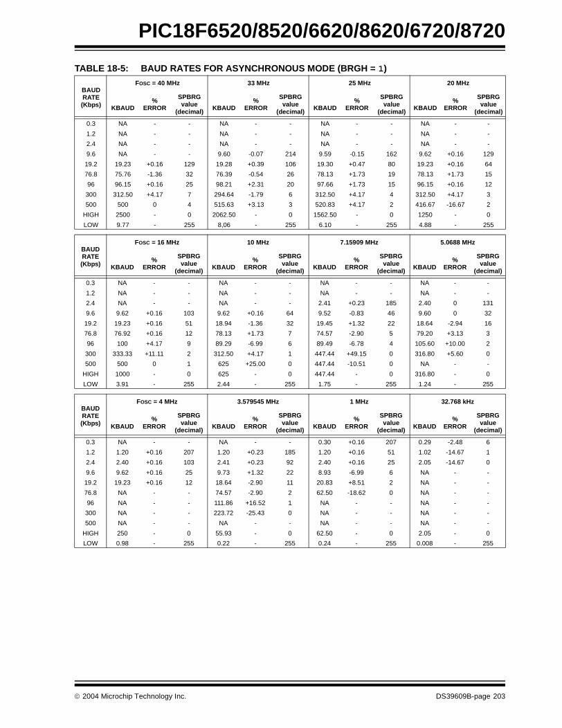
PIC18F6520/8520/6620/8620/6720/8720
TABLE 18-5: BAUD RATES FOR ASYNCHRONOUS MODE (BRGH = 1)
BAUDRATE(Kbps)
FOSC = 40 MHz 33 MHz 25 MHz 20 MHz
KBAUD%
ERROR
SPBRGvalue
(decimal) KBAUD%
ERROR
SPBRGvalue
(decimal) KBAUD%
ERROR
SPBRGvalue
(decimal) KBAUD%
ERROR
SPBRGvalue
(decimal)
0.3 NA - - NA - - NA - - NA - -
1.2 NA - - NA - - NA - - NA - -
2.4 NA - - NA - - NA - - NA - -
9.6 NA - - 9.60 -0.07 214 9.59 -0.15 162 9.62 +0.16 129
19.2 19.23 +0.16 129 19.28 +0.39 106 19.30 +0.47 80 19.23 +0.16 64
76.8 75.76 -1.36 32 76.39 -0.54 26 78.13 +1.73 19 78.13 +1.73 15
96 96.15 +0.16 25 98.21 +2.31 20 97.66 +1.73 15 96.15 +0.16 12
300 312.50 +4.17 7 294.64 -1.79 6 312.50 +4.17 4 312.50 +4.17 3
500 500 0 4 515.63 +3.13 3 520.83 +4.17 2 416.67 -16.67 2
HIGH 2500 - 0 2062.50 - 0 1562.50 - 0 1250 - 0
LOW 9.77 - 255 8,06 - 255 6.10 - 255 4.88 - 255
BAUDRATE(Kbps)
FOSC = 16 MHz 10 MHz 7.15909 MHz 5.0688 MHz
KBAUD%
ERROR
SPBRGvalue
(decimal) KBAUD%
ERROR
SPBRGvalue
(decimal) KBAUD%
ERROR
SPBRGvalue
(decimal) KBAUD%
ERROR
SPBRGvalue
(decimal)
0.3 NA - - NA - - NA - - NA - -
1.2 NA - - NA - - NA - - NA - -
2.4 NA - - NA - - 2.41 +0.23 185 2.40 0 131
9.6 9.62 +0.16 103 9.62 +0.16 64 9.52 -0.83 46 9.60 0 32
19.2 19.23 +0.16 51 18.94 -1.36 32 19.45 +1.32 22 18.64 -2.94 16
76.8 76.92 +0.16 12 78.13 +1.73 7 74.57 -2.90 5 79.20 +3.13 3
96 100 +4.17 9 89.29 -6.99 6 89.49 -6.78 4 105.60 +10.00 2
300 333.33 +11.11 2 312.50 +4.17 1 447.44 +49.15 0 316.80 +5.60 0
500 500 0 1 625 +25.00 0 447.44 -10.51 0 NA - -
HIGH 1000 - 0 625 - 0 447.44 - 0 316.80 - 0
LOW 3.91 - 255 2.44 - 255 1.75 - 255 1.24 - 255
BAUDRATE(Kbps)
FOSC = 4 MHz 3.579545 MHz 1 MHz 32.768 kHz
KBAUD%
ERROR
SPBRGvalue
(decimal) KBAUD%
ERROR
SPBRGvalue
(decimal) KBAUD%
ERROR
SPBRGvalue
(decimal) KBAUD%
ERROR
SPBRGvalue
(decimal)
0.3 NA - - NA - - 0.30 +0.16 207 0.29 -2.48 6
1.2 1.20 +0.16 207 1.20 +0.23 185 1.20 +0.16 51 1.02 -14.67 1
2.4 2.40 +0.16 103 2.41 +0.23 92 2.40 +0.16 25 2.05 -14.67 0
9.6 9.62 +0.16 25 9.73 +1.32 22 8.93 -6.99 6 NA - -
19.2 19.23 +0.16 12 18.64 -2.90 11 20.83 +8.51 2 NA - -
76.8 NA - - 74.57 -2.90 2 62.50 -18.62 0 NA - -
96 NA - - 111.86 +16.52 1 NA - - NA - -
300 NA - - 223.72 -25.43 0 NA - - NA - -
500 NA - - NA - - NA - - NA - -
HIGH 250 - 0 55.93 - 0 62.50 - 0 2.05 - 0
LOW 0.98 - 255 0.22 - 255 0.24 - 255 0.008 - 255
2004 Microchip Technology Inc. DS39609B-page 203

PIC18F6520/8520/6620/8620/6720/8720
18.2 USART Asynchronous Mode
In this mode, the USARTs use standard Non-Return-to-Zero (NRZ) format (one Start bit, eight or nine data bitsand one Stop bit). The most common data format is8 bits. An on-chip dedicated 8-bit Baud Rate Generatorcan be used to derive standard baud rate frequenciesfrom the oscillator. The USART transmits and receivesthe LSb first. The USART’s transmitter and receiver arefunctionally independent, but use the same data formatand baud rate. The Baud Rate Generator produces aclock, either 16 or 64 times the bit shift rate, dependingon bit BRGH (TXSTAx<2>). Parity is not supported bythe hardware, but can be implemented in software (andstored as the ninth data bit). Asynchronous mode isstopped during Sleep.
Asynchronous mode is selected by clearing bit SYNC(TXSTAx<4>).
The USART Asynchronous module consists of thefollowing important elements:
• Baud Rate Generator
• Sampling Circuit• Asynchronous Transmitter• Asynchronous Receiver
18.2.1 USART ASYNCHRONOUS TRANSMITTER
The USART transmitter block diagram is shown inFigure 18-1. The heart of the transmitter is the Transmit(Serial) Shift Register (TSR). The shift register obtainsits data from the Read/Write Transmit Buffer register,TXREGx. The TXREGx register is loaded with data insoftware. The TSR register is not loaded until the Stopbit has been transmitted from the previous load. Assoon as the Stop bit is transmitted, the TSR is loadedwith new data from the TXREGx register (if available).Once the TXREGx register transfers the data to theTSR register (occurs in one TCY), the TXREGx registeris empty and flag bit, TXx1IF (PIR1<4> for USART1,
PIR3<4> for USART2), is set. This interrupt can beenabled/disabled by setting/clearing enable bit, TXxIE(PIE1<4> for USART1, PIE<4> for USART2). Flag bitTXxIF will be set, regardless of the state of enable bitTXxIE and cannot be cleared in software. It will resetonly when new data is loaded into the TXREGx register.While flag bit TXIF indicates the status of the TXREGxregister, another bit, TRMT (TXSTAx<1>), shows thestatus of the TSR register. Status bit TRMT is a read-onlybit, which is set when the TSR register is empty. Nointerrupt logic is tied to this bit, so the user has to poll thisbit in order to determine if the TSR register is empty.
To set up an Asynchronous Transmission:
1. Initialize the SPBRGx register for the appropri-ate baud rate. If a high-speed baud rate isdesired, set bit BRGH (Section 18.1 “USARTBaud Rate Generator (BRG)”).
2. Enable the asynchronous serial port by clearingbit SYNC and setting bit SPEN.
3. If interrupts are desired, set enable bit TXxIE inthe appropriate PIE register.
4. If 9-bit transmission is desired, set transmit bitTX9. Can be used as address/data bit.
5. Enable the transmission by setting bit TXEN,which will also set bit TXxIF.
6. If 9-bit transmission is selected, the ninth bitshould be loaded in bit TX9D.
7. Load data to the TXREGx register (startstransmission).
FIGURE 18-1: USART TRANSMIT BLOCK DIAGRAM
Note 1: The TSR register is not mapped in datamemory, so it is not available to the user.
2: Flag bit TXIF is set when enable bit TXENis set.
Note: TXIF is not cleared immediately uponloading data into the transmit bufferTXREG. The flag bit becomes valid in thesecond instruction cycle following the loadinstruction.
TXIFTXIE
Interrupt
TXEN Baud Rate CLK
SPBRG
Baud Rate GeneratorTX9D
MSb LSb
Data Bus
TXREG Register
TSR Register
(8) 0
TX9
TRMT SPEN
TX pin
Pin Bufferand Control
8
• • •
DS39609B-page 204 2004 Microchip Technology Inc.

PIC18F6520/8520/6620/8620/6720/8720
FIGURE 18-2: ASYNCHRONOUS TRANSMISSION
FIGURE 18-3: ASYNCHRONOUS TRANSMISSION (BACK TO BACK)
TABLE 18-6: REGISTERS ASSOCIATED WITH ASYNCHRONOUS TRANSMISSION
Word 1Stop bit
Word 1Transmit Shift Reg
Start bit bit 0 bit 1 bit 7/8
Write to TXREGWord 1
BRG Output(Shift Clock)
RC6/TX1/CK1 (pin)
TXIF bit(Transmit Buffer
Reg. Empty Flag)
TRMT bit(Transmit ShiftReg. Empty Flag)
Transmit Shift Reg.
Write to TXREG
BRG Output(Shift Clock)
RC6/TX1/CK1 (pin)
TXIF bit(Interrupt Reg. Flag)
TRMT bit(Transmit Shift
Reg. Empty Flag)
Word 1 Word 2
Word 1 Word 2
Start bit Stop bit Start bit
Transmit Shift Reg.
Word 1 Word 2bit 0 bit 1 bit 7/8 bit 0
Note: This timing diagram shows two consecutive transmissions.
Name Bit 7 Bit 6 Bit 5 Bit 4 Bit 3 Bit 2 Bit 1 Bit 0Value on
POR, BOR
Value onall otherResets
INTCON GIE/GIEH PEIE/GIEL TMR0IE INT0IE RBIE TMR0IF INT0IF RBIF 0000 0000 0000 0000
PIR1 PSPIF ADIF RC1IF TX1IF SSPIF CCP1IF TMR2IF TMR1IF 0000 0000 0000 0000
PIE1 PSPIE ADIE RC1IE TX1IE SSPIE CCP1IE TMR2IE TMR1IE 0000 0000 0000 0000
IPR1 PSPIP ADIP RC1IP TX1IP SSPIP CCP1IP TMR2IP TMR1IP 0111 1111 0111 1111
PIR3 — — RC2IF TX2IF TMR4IF CCP5IF CCP4IF CCP3IF --00 0000 --00 0000
PIE3 — — RC2IE TX2IE TMR4IE CCP5IE CCP4IE CCP3IE --00 0000 --00 0000
IPR3 — — RC2IP TX2IP TMR4IP CCP5IP CCP4IP CCP3IP --11 1111 --11 1111
RCSTAx(1) SPEN RX9 SREN CREN ADDEN FERR OERR RX9D 0000 000x 0000 000x
TXREGx(1) USART Transmit Register 0000 0000 0000 0000
TXSTAx(1) CSRC TX9 TXEN SYNC — BRGH TRMT TX9D 0000 -010 0000 -010
SPBRGx(1) Baud Rate Generator Register 0000 0000 0000 0000
Legend: x = unknown, – = unimplemented locations read as ‘0’. Shaded cells are not used for asynchronous transmission.Note 1: Register names generically refer to both of the identically named registers for the two USART modules, where ‘x’
indicates the particular module. Bit names and Reset values are identical between modules.
2004 Microchip Technology Inc. DS39609B-page 205

PIC18F6520/8520/6620/8620/6720/8720
18.2.2 USART ASYNCHRONOUS RECEIVER
The USART receiver block diagram is shown inFigure 18-4. The data is received on the pin (RC7/RX1/DT1 or RG2/RX2/DT2) and drives the data recoveryblock. The data recovery block is actually a high-speedshifter operating at 16 times the baud rate, whereas themain receive serial shifter operates at the bit rate or atFOSC. This mode would typically be used in RS-232systems.
To set up an Asynchronous Reception:
1. Initialize the SPBRG register for the appropriatebaud rate. If a high-speed baud rate is desired,set bit BRGH (Section 18.1 “USART BaudRate Generator (BRG)”).
2. Enable the asynchronous serial port by clearingbit SYNC and setting bit SPEN.
3. If interrupts are desired, set enable bit RCxIE.
4. If 9-bit reception is desired, set bit RX9.5. Enable the reception by setting bit CREN.6. Flag bit RCxIF will be set when reception is com-
plete and an interrupt will be generated if enablebit RCxIE was set.
7. Read the RCSTAx register to get the ninth bit (ifenabled) and determine if any error occurredduring reception.
8. Read the 8-bit received data by reading theRCREG register.
9. If any error occurred, clear the error by clearingenable bit CREN.
10. If using interrupts, ensure that the GIE and PEIEbits in the INTCON register (INTCON<7:6>) areset.
18.2.3 SETTING UP 9-BIT MODE WITH ADDRESS DETECT
This mode would typically be used in RS-485 systems.To set up an Asynchronous Reception with AddressDetect Enable:
1. Initialize the SPBRGx register for the appropri-ate baud rate. If a high-speed baud rate isrequired, set the BRGH bit.
2. Enable the asynchronous serial port by clearingthe SYNC bit and setting the SPEN bit.
3. If interrupts are required, set the RCEN bit andselect the desired priority level with the RCIP bit.
4. Set the RX9 bit to enable 9-bit reception.
5. Set the ADDEN bit to enable address detect. 6. Enable reception by setting the CREN bit.7. The RCxIF bit will be set when reception is
complete. The interrupt will be Acknowledged ifthe RCxIE and GIE bits are set.
8. Read the RCSTAx register to determine if anyerror occurred during reception, as well as readbit 9 of data (if applicable).
9. Read RCREGx to determine if the device isbeing addressed.
10. If any error occurred, clear the CREN bit. 11. If the device has been addressed, clear the
ADDEN bit to allow all received data into thereceive buffer and interrupt the CPU.
FIGURE 18-4: USART RECEIVE BLOCK DIAGRAM
x64 Baud Rate CLK
SPBRG
Baud Rate Generator
RX pin
Pin Bufferand Control
SPEN
DataRecovery
CREN OERR FERR
RSR RegisterMSb LSb
RX9D RCREG RegisterFIFO
Interrupt RCIF
RCIE
Data Bus
8
÷ 64
÷ 16or
Stop Start(8) 7 1 0
RX9
• • •
DS39609B-page 206 2004 Microchip Technology Inc.

PIC18F6520/8520/6620/8620/6720/8720
FIGURE 18-5: ASYNCHRONOUS RECEPTION
TABLE 18-7: REGISTERS ASSOCIATED WITH ASYNCHRONOUS RECEPTION
Startbit bit 7/8bit 1bit 0 bit 7/8 bit 0Stop
bit
Startbit
Startbitbit 7/8 Stop
bit
RX (pin)
RegRcv Buffer Reg
Rcv Shift
Read RcvBuffer RegRCREG
RCIF(Interrupt Flag)
OERR bit
CREN
Word 1RCREG
Word 2RCREG
Stopbit
Note: This timing diagram shows three words appearing on the RX input. The RCREG (receive buffer) is read after the third word, causing the OERR (overrun) bit to be set.
Name Bit 7 Bit 6 Bit 5 Bit 4 Bit 3 Bit 2 Bit 1 Bit 0Value on
POR, BOR
Value onall otherResets
INTCON GIE/GIEH
PEIE/GIEL
TMR0IE INT0IE RBIE TMR0IF INT0IF RBIF 0000 0000 0000 0000
PIR1 PSPIF ADIF RC1IF TXIF SSPIF CCP1IF TMR2IF TMR1IF 0000 0000 0000 0000
PIE1 PSPIE ADIE RC1IE TXIE SSPIE CCP1IE TMR2IE TMR1IE 0000 0000 0000 0000
IPR1 PSPIP ADIP RC1IP TXIP SSPIP CCP1IP TMR2IP TMR1IP 0111 1111 0111 1111
PIR3 — — RC2IF TX2IF TMR4IF CCP5IF CCP4IF CCP3IF --00 0000 --00 0000
PIE3 — — RC2IE TX2IE TMR4IE CCP5IE CCP4IE CCP3IE --00 0000 --00 0000
IPR3 — — RC2IP TX2IP TMR4IP CCP5IP CCP4IP CCP3IP --11 1111 --11 1111
RCSTAx(1) SPEN RX9 SREN CREN ADDEN FERR OERR RX9D 0000 000x 0000 000x
RCREGx(1) USART Receive Register 0000 0000 0000 0000
TXSTAx(1) CSRC TX9 TXEN SYNC — BRGH TRMT TX9D 0000 -010 0000 -010
SPBRGx(1) Baud Rate Generator Register 0000 0000 0000 0000
Legend: x = unknown, – = unimplemented locations read as ‘0’. Shaded cells are not used for asynchronous reception.Note 1: Register names generically refer to both of the identically named registers for the two USART modules, where ‘x’
indicates the particular module. Bit names and Reset values are identical between modules.
2004 Microchip Technology Inc. DS39609B-page 207
PIC18F6520/8520/6620/8620/6720/8720
18.3 USART Synchronous Master Mode
In Synchronous Master mode, the data is transmitted ina half-duplex manner (i.e., transmission and receptiondo not occur at the same time). When transmitting data,the reception is inhibited and vice versa. Synchronousmode is entered by setting bit SYNC (TXSTAx<4>). Inaddition, enable bit SPEN (RCSTAx<7>) is set in orderto configure the appropriate I/O pins to CK (clock) andDT (data) lines, respectively. The Master mode indi-cates that the processor transmits the master clock onthe CK line. The Master mode is entered by setting bitCSRC (TXSTAx<7>).
18.3.1 USART SYNCHRONOUS MASTER TRANSMISSION
The USART transmitter block diagram is shown inFigure 18-1. The heart of the transmitter is the Transmit(Serial) Shift Register (TSR). The shift register obtainsits data from the Read/Write Transmit Buffer register,TXREG. The TXREGx register is loaded with data insoftware. The TSR register is not loaded until the lastbit has been transmitted from the previous load. Assoon as the last bit is transmitted, the TSR is loadedwith new data from the TXREGx (if available). Once theTXREGx register transfers the data to the TSR register(occurs in one TCYCLE), the TXREGx is empty andinterrupt bit TXxIF (PIR1<4> for USART1, PIR3<4> forUSART2) is set. The interrupt can be enabled/disabledby setting/clearing enable bit TXxIE (PIE1<4> forUSART1, PIE3<4> for USART2). Flag bit TXxIF will be
set, regardless of the state of enable bit TXxIE and can-not be cleared in software. It will reset only when newdata is loaded into the TXREGx register. While flag bitTXxIF indicates the status of the TXREGx register,another bit TRMT (TXSTAx<1>) shows the status of theTSR register. TRMT is a read-only bit, which is setwhen the TSR is empty. No interrupt logic is tied to thisbit, so the user has to poll this bit in order to determineif the TSR register is empty. The TSR is not mapped indata memory, so it is not available to the user.
To set up a Synchronous Master Transmission:
1. Initialize the SPBRG register for the appropriatebaud rate (Section 18.1 “USART Baud RateGenerator (BRG)”).
2. Enable the synchronous master serial port bysetting bits SYNC, SPEN and CSRC.
3. If interrupts are desired, set enable bit TXxIE inthe appropriate PIE register.
4. If 9-bit transmission is desired, set bit TX9.5. Enable the transmission by setting bit TXEN.6. If 9-bit transmission is selected, the ninth bit
should be loaded in bit TX9D.7. Start transmission by loading data to the
TXREGx register.
TABLE 18-8: REGISTERS ASSOCIATED WITH SYNCHRONOUS MASTER TRANSMISSION
Note: TXIF is not cleared immediately uponloading data into the transmit bufferTXREG. The flag bit becomes valid in thesecond instruction cycle following the loadinstruction.
Name Bit 7 Bit 6 Bit 5 Bit 4 Bit 3 Bit 2 Bit 1 Bit 0Value on
POR, BOR
Value on all other Resets
INTCON GIE/GIEH
PEIE/GIEL
TMR0IE INT0IE RBIE TMR0IF INT0IF RBIF 0000 0000 0000 0000
PIR1 PSPIF ADIF RCIF TXIF SSPIF CCP1IF TMR2IF TMR1IF 0000 0000 0000 0000
PIE1 PSPIE ADIE RCIE TXIE SSPIE CCP1IE TMR2IE TMR1IE 0000 0000 0000 0000
IPR1 PSPIP ADIP RCIP TXIP SSPIP CCP1IP TMR2IP TMR1IP 0111 1111 0111 1111
PIR3 — — RC2IF TX2IF TMR4IF CCP5IF CCP4IF CCP3IF --00 0000 --00 0000
PIE3 — — RC2IE TX2IE TMR4IE CCP5IE CCP4IE CCP3IE --00 0000 --00 0000
IPR3 — — RC2IP TX2IP TMR4IP CCP5IP CCP4IP CCP3IP --11 1111 --11 1111
RCSTAx(1) SPEN RX9 SREN CREN ADDEN FERR OERR RX9D 0000 000x 0000 000x
TXREGx(1) USART Transmit Register 0000 0000 0000 0000
TXSTAx(1) CSRC TX9 TXEN SYNC — BRGH TRMT TX9D 0000 -010 0000 -010
SPBRGx(1) Baud Rate Generator Register 0000 0000 0000 0000
Legend: x = unknown, – = unimplemented, read as ‘0’. Shaded cells are not used for synchronous master transmission.Note 1: Register names generically refer to both of the identically named registers for the two USART modules, where ‘x’
indicates the particular module. Bit names and Reset values are identical between modules.
DS39609B-page 208 2004 Microchip Technology Inc.

PIC18F6520/8520/6620/8620/6720/8720
FIGURE 18-6: SYNCHRONOUS TRANSMISSION
FIGURE 18-7: SYNCHRONOUS TRANSMISSION (THROUGH TXEN)
bit 0 bit 1 bit 7
Word 1
Q1 Q2 Q3Q4 Q1 Q2Q3 Q4 Q1 Q2Q3 Q4Q1 Q2 Q3 Q4Q1 Q2 Q3Q4 Q3Q4 Q1 Q2 Q3Q4 Q1Q2 Q3 Q4 Q1Q2 Q3 Q4Q1 Q2 Q3 Q4Q1 Q2Q3 Q4 Q1 Q2Q3 Q4
bit 2 bit 0 bit 1 bit 7RC7/RX1/DT1
RC6/TX1/CK1
Write toTXREG Reg
TXIF bit(Interrupt Flag)
TRMT
TXEN bit‘1’ ‘1’
Word 2
TRMT bit
Write Word 1 Write Word 2
Note: Sync Master mode; SPBRG = 0. Continuous transmission of two 8-bit words.
pin
pin
RC7/RX1/DT1 pin
RC6/TX1/CK1 pin
Write toTXREG reg
TXIF bit
TRMT bit
bit 0 bit 1 bit 2 bit 6 bit 7
TXEN bit
2004 Microchip Technology Inc. DS39609B-page 209

PIC18F6520/8520/6620/8620/6720/8720
18.3.2 USART SYNCHRONOUS MASTER RECEPTION
Once Synchronous mode is selected, reception isenabled by setting either enable bit SREN(RCSTAx<5>) or enable bit CREN (RCSTAx<4>). Datais sampled on the RXx pin (RC7/RX1/DT1 or RG2/RX2/DT2) on the falling edge of the clock. If enable bit SRENis set, only a single word is received. If enable bit CRENis set, the reception is continuous until CREN is cleared.If both bits are set, then CREN takes precedence.
To set up a Synchronous Master Reception:
1. Initialize the SPBRGx register for the appropri-ate baud rate (Section 18.1 “USART BaudRate Generator (BRG)”).
2. Enable the synchronous master serial port bysetting bits SYNC, SPEN and CSRC.
3. Ensure bits CREN and SREN are clear.
4. If interrupts are desired, set enable bit RCxIE inthe appropriate PIE register.
5. If 9-bit reception is desired, set bit RX9.6. If a single reception is required, set bit SREN.
For continuous reception, set bit CREN.7. Interrupt flag bit RCxIF will be set when
reception is complete and an interrupt will begenerated if the enable bit RCxIE was set.
8. Read the RCSTAx register to get the ninth bit (ifenabled) and determine if any error occurredduring reception.
9. Read the 8-bit received data by reading theRCREGx register.
10. If any error occurred, clear the error by clearingbit CREN.
11. If using interrupts, ensure that the GIE and PEIEbits in the INTCON register (INTCON<7:6>) areset.
TABLE 18-9: REGISTERS ASSOCIATED WITH SYNCHRONOUS MASTER RECEPTION
FIGURE 18-8: SYNCHRONOUS RECEPTION (MASTER MODE, SREN)
Name Bit 7 Bit 6 Bit 5 Bit 4 Bit 3 Bit 2 Bit 1 Bit 0Value on
POR, BOR
Value on all other Resets
INTCON GIE/GIEH PEIE/GIEL TMR0IE INT0IE RBIE TMR0IF INT0IF RBIF 0000 0000 0000 0000
PIR1 PSPIF ADIF RC1IF TX1IF SSPIF CCP1IF TMR2IF TMR1IF 0000 0000 0000 0000
PIE1 PSPIE ADIE RC1IE TX1IE SSPIE CCP1IE TMR2IE TMR1IE 0000 0000 0000 0000
IPR1 PSPIP ADIP RC1IP TX1IP SSPIP CCP1IP TMR2IP TMR1IP 0111 1111 0111 1111
PIR3 — — RC2IF TX2IF TMR4IF CCP5IF CCP4IF CCP3IF --00 0000 --00 0000
PIE3 — — RC2IE TX2IE TMR4IE CCP5IE CCP4IE CCP3IE --00 0000 --00 0000
IPR3 — — RC2IP TX2IP TMR4IP CCP5IP CCP4IP CCP3IP --11 1111 --11 1111
RCSTAx(1) SPEN RX9 SREN CREN ADDEN FERR OERR RX9D 0000 000x 0000 000x
RCREGx(1) USART Receive Register 0000 0000 0000 0000
TXSTAx(1) CSRC TX9 TXEN SYNC — BRGH TRMT TX9D 0000 -010 0000 -010
SPBRGx(1) Baud Rate Generator Register 0000 0000 0000 0000
Legend: x = unknown, – = unimplemented, read as ‘0’. Shaded cells are not used for synchronous master reception.Note 1: Register names generically refer to both of the identically named registers for the two USART modules, where ‘x’
indicates the particular module. Bit names and Reset values are identical between modules.
CREN bit
RC7/RX1/DT1 pin
RC6/TX1/CK1 pin
Write tobit SREN
SREN bit
RCIF bit(Interrupt)
ReadRXREG
Q3 Q4 Q1 Q2 Q3 Q4 Q1 Q2 Q3 Q4Q2 Q1 Q2 Q3 Q4 Q1 Q2 Q3 Q4 Q1 Q2 Q3 Q4 Q1 Q2 Q3 Q4 Q1 Q2 Q3 Q4 Q1 Q2 Q3 Q4 Q1 Q2 Q3 Q4
‘0’
bit 0 bit 1 bit 2 bit 3 bit 4 bit 5 bit 6 bit 7
‘0’
Q1 Q2 Q3 Q4
Note: Timing diagram demonstrates Sync Master mode with bit SREN = 1 and bit BRGH = 0.
DS39609B-page 210 2004 Microchip Technology Inc.

PIC18F6520/8520/6620/8620/6720/8720
18.4 USART Synchronous Slave Mode
Synchronous Slave mode differs from the Master modein the fact that the shift clock is supplied externally atthe TXx pin (RC6/TX1/CK1 or RG1/TX2/CK2), insteadof being supplied internally in Master mode. TRISC<6>must be set for this mode. This allows the device totransfer or receive data while in Sleep mode. Slavemode is entered by clearing bit CSRC (TXSTAx<7>).
18.4.1 USART SYNCHRONOUS SLAVE TRANSMIT
The operation of the Synchronous Master and Slavemodes are identical, except in the case of the Sleepmode.
If two words are written to the TXREG and then theSLEEP instruction is executed, the following will occur:
a) The first word will immediately transfer to theTSR register and transmit.
b) The second word will remain in TXREG register.
c) Flag bit TXxIF will not be set. d) When the first word has been shifted out of TSR,
the TXREGx register will transfer the secondword to the TSR and flag bit TXxIF will now beset.
e) If enable bit TXxIE is set, the interrupt will wakethe chip from Sleep. If the global interrupt isenabled, the program will branch to the interruptvector.
To set up a Synchronous Slave Transmission:
1. Enable the synchronous slave serial port bysetting bits SYNC and SPEN and clearing bitCSRC.
2. Clear bits CREN and SREN.3. If interrupts are desired, set enable bit TXxIE.4. If 9-bit transmission is desired, set bit TX9.
5. Enable the transmission by setting enable bitTXEN.
6. If 9-bit transmission is selected, the ninth bitshould be loaded in bit TX9D.
7. Start transmission by loading data to theTXREGx register.
8. If using interrupts, ensure that the GIE and PEIEbits in the INTCON register (INTCON<7:6>) areset.
TABLE 18-10: REGISTERS ASSOCIATED WITH SYNCHRONOUS SLAVE TRANSMISSION
Name Bit 7 Bit 6 Bit 5 Bit 4 Bit 3 Bit 2 Bit 1 Bit 0Value on
POR, BOR
Value on all other Resets
INTCON GIE/GIEH
PEIE/GIEL
TMR0IE INT0IE RBIE TMR0IF INT0IF RBIF 0000 0000 0000 0000
PIR1 PSPIF ADIF RC1IF TX1IF SSPIF CCP1IF TMR2IF TMR1IF 0000 0000 0000 0000
PIE1 PSPIE ADIE RC1IE TX1IE SSPIE CCP1IE TMR2IE TMR1IE 0000 0000 0000 0000
IPR1 PSPIP ADIP RC1IP TX1IP SSPIP CCP1IP TMR2IP TMR1IP 0111 1111 0111 1111
PIR3 — — RC2IF TX2IF TMR4IF CCP5IF CCP4IF CCP3IF --00 0000 --00 0000
PIE3 — — RC2IE TX2IE TMR4IE CCP5IE CCP4IE CCP3IE --00 0000 --00 0000
IPR3 — — RC2IP TX2IP TMR4IP CCP5IP CCP4IP CCP3IP --11 1111 --11 1111
RCSTAx(1) SPEN RX9 SREN CREN ADDEN FERR OERR RX9D 0000 000x 0000 000x
TXREGx(1) USART Transmit Register 0000 0000 0000 0000
TXSTAx(1) CSRC TX9 TXEN SYNC — BRGH TRMT TX9D 0000 -010 0000 -010
SPBRGx(1) Baud Rate Generator Register 0000 0000 0000 0000
Legend: x = unknown, – = unimplemented, read as ‘0’. Shaded cells are not used for synchronous slave transmission.Note 1: Register names generically refer to both of the identically named registers for the two USART modules, where ‘x’
indicates the particular module. Bit names and Reset values are identical between modules.
2004 Microchip Technology Inc. DS39609B-page 211

PIC18F6520/8520/6620/8620/6720/8720
18.4.2 USART SYNCHRONOUS SLAVE RECEPTION
The operation of the Synchronous Master and Slavemodes is identical, except in the case of the Sleepmode and bit SREN, which is a “don’t care” in Slavemode.
If receive is enabled by setting bit CREN prior to theSLEEP instruction, then a word may be received duringSleep. On completely receiving the word, the RSR reg-ister will transfer the data to the RCREG register and ifenable bit RCxIE bit is set, the interrupt generated willwake the chip from Sleep. If the global interrupt isenabled, the program will branch to the interrupt vector.
To set up a Synchronous Slave Reception:
1. Enable the synchronous master serial port bysetting bits SYNC and SPEN and clearing bitCSRC.
2. If interrupts are desired, set enable bit RCxIE.3. If 9-bit reception is desired, set bit RX9.4. To enable reception, set enable bit CREN.
5. Flag bit RCxIF will be set when reception iscomplete. An interrupt will be generated ifenable bit RCxIE was set.
6. Read the RCSTAx register to get the ninth bit (ifenabled) and determine if any error occurredduring reception.
7. Read the 8-bit received data by reading theRCREGx register.
8. If any error occurred, clear the error by clearingbit CREN.
9. If using interrupts, ensure that the GIE and PEIEbits in the INTCON register (INTCON<7:6>) areset.
TABLE 18-11: REGISTERS ASSOCIATED WITH SYNCHRONOUS SLAVE RECEPTION
Name Bit 7 Bit 6 Bit 5 Bit 4 Bit 3 Bit 2 Bit 1 Bit 0Value on
POR, BOR
Value on all other Resets
INTCON GIE/GIEH
PEIE/GIEL
TMR0IE INT0IE RBIE TMR0IF INT0IF RBIF 0000 0000 0000 0000
PIR1 PSPIF ADIF RC1IF TX1IF SSPIF CCP1IF TMR2IF TMR1IF 0000 0000 0000 0000
PIE1 PSPIE ADIE RC1IE TX1IE SSPIE CCP1IE TMR2IE TMR1IE 0000 0000 0000 0000
IPR1 PSPIP ADIP RC1IP TX1IP SSPIP CCP1IP TMR2IP TMR1IP 0111 1111 0111 1111
PIR3 — — RC2IF TX2IF TMR4IF CCP5IF CCP4IF CCP3IF --00 0000 --00 0000
PIE3 — — RC2IE TX2IE TMR4IE CCP5IE CCP4IE CCP3IE --00 0000 --00 0000
IPR3 — — RC2IP TX2IP TMR4IP CCP5IP CCP4IP CCP3IP --11 1111 --11 1111
RCSTAx(1) SPEN RX9 SREN CREN ADDEN FERR OERR RX9D 0000 000x 0000 000x
RCREGx(1) USART Receive Register 0000 0000 0000 0000
TXSTAx(1) CSRC TX9 TXEN SYNC — BRGH TRMT TX9D 0000 -010 0000 -010
SPBRGx(1) Baud Rate Generator Register 0000 0000 0000 0000
Legend: x = unknown, – = unimplemented, read as ‘0’. Shaded cells are not used for synchronous slave reception.Note 1: Register names generically refer to both of the identically named registers for the two USART modules, where ‘x’
indicates the particular module. Bit names and Reset values are identical between modules.
DS39609B-page 212 2004 Microchip Technology Inc.

PIC18F6520/8520/6620/8620/6720/8720
19.0 10-BIT ANALOG-TO-DIGITAL CONVERTER (A/D) MODULE
The analog-to-digital (A/D) converter module has 12inputs for the PIC18F6X20 devices and 16 for thePIC18F8X20 devices. This module allows conversionof an analog input signal to a corresponding 10-bitdigital number.
The module has five registers:
• A/D Result High Register (ADRESH)• A/D Result Low Register (ADRESL)
• A/D Control Register 0 (ADCON0)• A/D Control Register 1 (ADCON1)• A/D Control Register 2 (ADCON2)
The ADCON0 register, shown in Register 19-1, con-trols the operation of the A/D module. The ADCON1register, shown in Register 19-2, configures the func-tions of the port pins. The ADCON2 register, shown inRegister 19-3, configures the A/D clock source andjustification.
REGISTER 19-1: ADCON0 REGISTER U-0 U-0 R/W-0 R/W-0 R/W-0 R/W-0 R/W-0 R/W-0
— — CHS3 CHS2 CHS1 CHS0 GO/DONE ADON
bit 7 bit 0
bit 7-6 Unimplemented: Read as ‘0’
bit 5-2 CHS3:CHS0: Analog Channel Select bits0000 = Channel 0 (AN0) 0001 = Channel 1 (AN1) 0010 = Channel 2 (AN2) 0011 = Channel 3 (AN3) 0100 = Channel 4 (AN4) 0101 = Channel 5 (AN5) 0110 = Channel 6 (AN6) 0111 = Channel 7 (AN7) 1000 = Channel 8 (AN8) 1001 = Channel 9 (AN9) 1010 = Channel 10 (AN10) 1011 = Channel 11 (AN11) 1100 = Channel 12 (AN12)(1) 1101 = Channel 13 (AN13)(1) 1110 = Channel 14 (AN14)(1) 1111 = Channel 15 (AN15)(1)
Note 1: These channels are not available on the PIC18F6X20 (64-pin) devices.
bit 1 GO/DONE: A/D Conversion Status bitWhen ADON = 1: 1 = A/D conversion in progress (setting this bit starts the A/D conversion, which is automatically
cleared by hardware when the A/D conversion is complete)0 = A/D conversion not in progress
bit 0 ADON: A/D On bit1 = A/D converter module is enabled 0 = A/D converter module is disabled
Legend:
R = Readable bit W = Writable bit U = Unimplemented bit, read as ‘0’
- n = Value at POR ‘1’ = Bit is set ‘0’ = Bit is cleared x = Bit is unknown
2004 Microchip Technology Inc. DS39609B-page 213
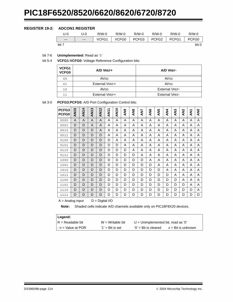
PIC18F6520/8520/6620/8620/6720/8720
REGISTER 19-2: ADCON1 REGISTER U-0 U-0 R/W-0 R/W-0 R/W-0 R/W-0 R/W-0 R/W-0
— — VCFG1 VCFG0 PCFG3 PCFG2 PCFG1 PCFG0
bit 7 bit 0
bit 7-6 Unimplemented: Read as ‘0’
bit 5-4 VCFG1:VCFG0: Voltage Reference Configuration bits:
bit 3-0 PCFG3:PCFG0: A/D Port Configuration Control bits:
Legend:
R = Readable bit W = Writable bit U = Unimplemented bit, read as ‘0’
- n = Value at POR ‘1’ = Bit is set ‘0’ = Bit is cleared x = Bit is unknown
VCFG1VCFG0
A/D VREF+ A/D VREF-
00 AVDD AVSS
01 External VREF+ AVSS
10 AVDD External VREF-
11 External VREF+ External VREF-
A = Analog input D = Digital I/O
Note: Shaded cells indicate A/D channels available only on PIC18F8X20 devices.
PCFG3PCFG0 A
N15
AN
14
AN
13
AN
12
AN
11
AN
10
AN
9
AN
8
AN
7
AN
6
AN
5
AN
4
AN
3
AN
2
AN
1
AN
0
0000 A A A A A A A A A A A A A A A A0001 D D A A A A A A A A A A A A A A
0010 D D D A A A A A A A A A A A A A0011 D D D D A A A A A A A A A A A A0100 D D D D D A A A A A A A A A A A
0101 D D D D D D A A A A A A A A A A0110 D D D D D D D A A A A A A A A A0111 D D D D D D D D A A A A A A A A
1000 D D D D D D D D D A A A A A A A1001 D D D D D D D D D D A A A A A A1010 D D D D D D D D D D D A A A A A
1011 D D D D D D D D D D D D A A A A1100 D D D D D D D D D D D D D A A A1101 D D D D D D D D D D D D D D A A
1110 D D D D D D D D D D D D D D D A1111 D D D D D D D D D D D D D D D D
DS39609B-page 214 2004 Microchip Technology Inc.
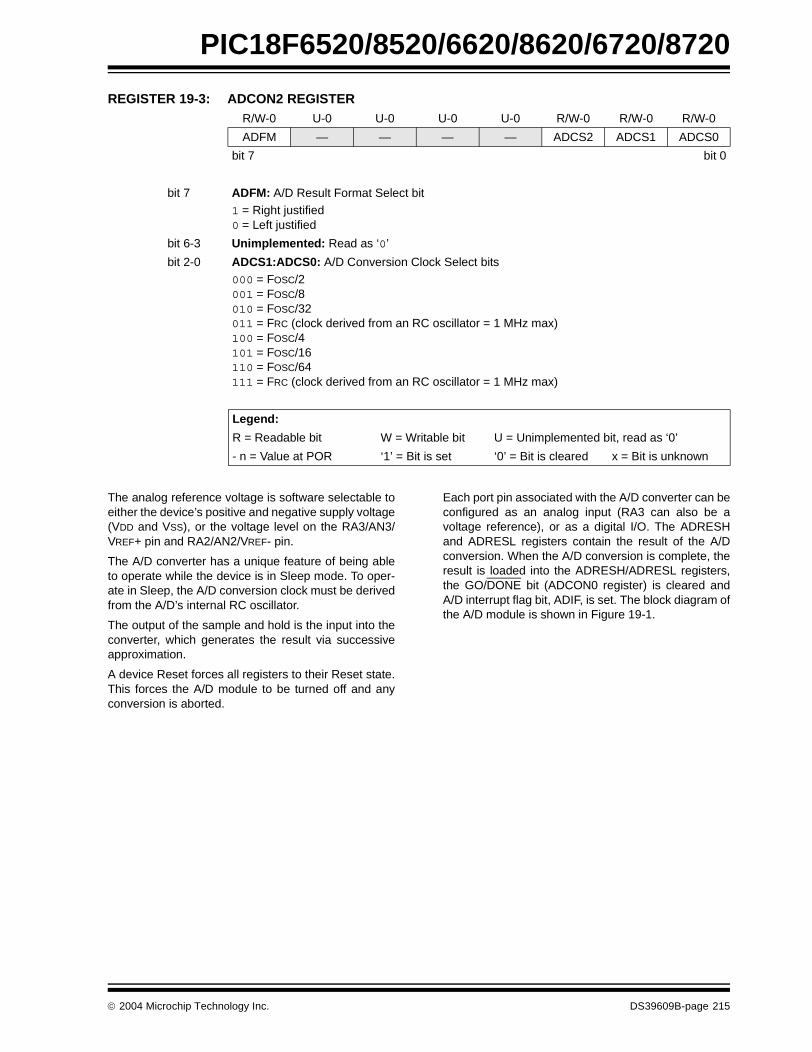
PIC18F6520/8520/6620/8620/6720/8720
REGISTER 19-3: ADCON2 REGISTER
The analog reference voltage is software selectable toeither the device’s positive and negative supply voltage(VDD and VSS), or the voltage level on the RA3/AN3/VREF+ pin and RA2/AN2/VREF- pin.
The A/D converter has a unique feature of being ableto operate while the device is in Sleep mode. To oper-ate in Sleep, the A/D conversion clock must be derivedfrom the A/D’s internal RC oscillator.
The output of the sample and hold is the input into theconverter, which generates the result via successiveapproximation.
A device Reset forces all registers to their Reset state.This forces the A/D module to be turned off and anyconversion is aborted.
Each port pin associated with the A/D converter can beconfigured as an analog input (RA3 can also be avoltage reference), or as a digital I/O. The ADRESHand ADRESL registers contain the result of the A/Dconversion. When the A/D conversion is complete, theresult is loaded into the ADRESH/ADRESL registers,the GO/DONE bit (ADCON0 register) is cleared andA/D interrupt flag bit, ADIF, is set. The block diagram ofthe A/D module is shown in Figure 19-1.
R/W-0 U-0 U-0 U-0 U-0 R/W-0 R/W-0 R/W-0
ADFM — — — — ADCS2 ADCS1 ADCS0
bit 7 bit 0
bit 7 ADFM: A/D Result Format Select bit1 = Right justified 0 = Left justified
bit 6-3 Unimplemented: Read as ‘0’
bit 2-0 ADCS1:ADCS0: A/D Conversion Clock Select bits000 = FOSC/2 001 = FOSC/8 010 = FOSC/32 011 = FRC (clock derived from an RC oscillator = 1 MHz max) 100 = FOSC/4 101 = FOSC/16 110 = FOSC/64 111 = FRC (clock derived from an RC oscillator = 1 MHz max)
Legend:
R = Readable bit W = Writable bit U = Unimplemented bit, read as ‘0’
- n = Value at POR ‘1’ = Bit is set ‘0’ = Bit is cleared x = Bit is unknown
2004 Microchip Technology Inc. DS39609B-page 215

PIC18F6520/8520/6620/8620/6720/8720
FIGURE 19-1: A/D BLOCK DIAGRAM
(Input Voltage)
VAIN
VREF+ReferenceVoltage
VDD
VCFG1:VCFG0
CHS3:CHS0
AN7
AN6
AN5
AN4
AN3
AN2
AN1
AN0
0111
0110
0101
0100
0011
0010
0001
0000
10-bitConverter
VREF-
VSS
A/D
AN15(1)
AN14(1)
AN13(1)
AN12(1)
AN11
AN10
AN9
AN8
1111
1110
1101
1100
1011
1010
1001
1000
Note 1: Channels AN15 through AN12 are not available on PIC18F6X20 devices.
2: I/O pins have diode protection to VDD and VSS.
DS39609B-page 216 2004 Microchip Technology Inc.

PIC18F6520/8520/6620/8620/6720/8720
The value in the ADRESH/ADRESL registers is notmodified for a Power-on Reset. The ADRESH/ADRESL registers will contain unknown data after aPower-on Reset.
After the A/D module has been configured as desired,the selected channel must be acquired before the con-version is started. The analog input channels musthave their corresponding TRIS bits selected as aninput. To determine acquisition time, see Section 19.1“A/D Acquisition Requirements”. After this acquisi-tion time has elapsed, the A/D conversion can bestarted.
The following steps should be followed to do an A/Dconversion:
1. Configure the A/D module:
• Configure analog pins, voltage reference and digital I/O (ADCON1)
• Select A/D input channel (ADCON0)• Select A/D conversion clock (ADCON2)• Turn on A/D module (ADCON0)
2. Configure A/D interrupt (if desired):• Clear ADIF bit • Set ADIE bit • Set GIE bit
3. Wait the required acquisition time.4. Start conversion:
• Set GO/DONE bit (ADCON0 register)
5. Wait for A/D conversion to complete, by either:• Polling for the GO/DONE bit to be clearedOR• Waiting for the A/D interrupt
6. Read A/D Result registers (ADRESH:ADRESL);clear bit ADIF, if required.
7. For the next conversion, go to step 1 or step 2,as required. The A/D conversion time per bit isdefined as TAD. A minimum wait of 2 TAD isrequired before the next acquisition starts.
FIGURE 19-2: ANALOG INPUT MODEL
VAINCPIN
Rs ANx
5 pF
VDD
VT = 0.6V
VT = 0.6VILEAKAGE
RIC ≤ 1k
SamplingSwitch
SS RSS
CHOLD = 120 pF
VSS
6V
Sampling Switch
5V4V3V2V
5 6 7 8 9 10 11
(kΩ)
VDD
± 500 nA
Legend: CPIN
VT
ILEAKAGE
RIC
SSCHOLD
= input capacitance
= threshold voltage= leakage current at the pin due to
= interconnect resistance= sampling switch= sample/hold capacitance (from DAC)
various junctions
= sampling switch resistanceRSS
2004 Microchip Technology Inc. DS39609B-page 217

PIC18F6520/8520/6620/8620/6720/8720
19.1 A/D Acquisition Requirements
For the A/D converter to meet its specified accuracy,the charge holding capacitor (CHOLD) must be allowedto fully charge to the input channel voltage level. Theanalog input model is shown in Figure 19-2. Thesource impedance (RS) and the internal samplingswitch (RSS) impedance directly affect the timerequired to charge the capacitor CHOLD. The samplingswitch (RSS) impedance varies over the device voltage(VDD). The source impedance affects the offset voltageat the analog input (due to pin leakage current). Themaximum recommended impedance for analogsources is 2.5 kΩ. After the analog input channel isselected (changed), this acquisition must be donebefore the conversion can be started.
To calculate the minimum acquisition time,Equation 19-1 may be used. This equation assumesthat 1/2 LSb error is used (1024 steps for the A/D). The1/2 LSb error is the maximum error allowed for the A/Dto meet its specified resolution.
Example 19-1 shows the calculation of the minimumrequired acquisition time, TACQ. This calculation isbased on the following application systemassumptions:
CHOLD = 120 pF Rs = 2.5 kΩ Conversion Error ≤ 1/2 LSb VDD = 5V → Rss = 7 kΩ Temperature = 50°C (system max.) VHOLD = 0V @ time = 0
EQUATION 19-1: ACQUISITION TIME
EQUATION 19-2: A/D MINIMUM CHARGING TIME
EXAMPLE 19-1: CALCULATING THE MINIMUM REQUIRED ACQUISITION TIME
Note: When the conversion is started, theholding capacitor is disconnected from theinput pin.
Note: When using external voltage references withthe A/D converter, the source impedance ofthe external voltage references must be lessthan 20Ω to obtain the A/D performancespecified in parameters A01-A06. Higherreference source impedances will increaseboth offset and gain errors. Resistive voltagedividers will not provide a sufficiently lowsource impedance.
To maintain the best possible performance inA/D conversions, external VREF inputs shouldbe buffered with an operational amplifier orother low output impedance circuit.
If deviating from the operating conditionsspecified for parameters A03-A06, the effectof parameter A50 (VREF input current) mustbe considered.
TACQ = Amplifier Settling Time + Holding Capacitor Charging Time + Temperature Coefficient
= TAMP + TC + TCOFF
VHOLD = (VREF – (VREF/2048)) • (1 – e(-Tc/CHOLD(RIC + RSS + RS))) or TC = -(120 pF)(1 kΩ + RSS + RS) ln(1/2047)
TACQ = TAMP + TC + TCOFF
Temperature coefficient is only required for temperatures > 25°C.
TACQ = 2 µs + TC + [(Temp – 25°C)(0.05 µs/°C)]
TC = -CHOLD (RIC + RSS + RS) ln(1/2047) -120 pF (1 kΩ + 7 kΩ + 2.5 kΩ) ln(0.0004885) -120 pF (10.5 kΩ) ln(0.0004885) -1.26 µs (-7.6241) 9.61 µs
TACQ = 2 µs + 9.61 µs + [(50°C – 25°C)(0.05 µs/°C)] 11.61 µs + 1.25 µs 12.86 µs
DS39609B-page 218 2004 Microchip Technology Inc.
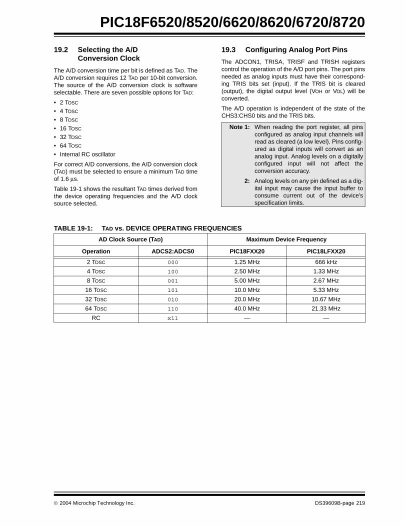
PIC18F6520/8520/6620/8620/6720/8720
19.2 Selecting the A/D Conversion Clock
The A/D conversion time per bit is defined as TAD. TheA/D conversion requires 12 TAD per 10-bit conversion.The source of the A/D conversion clock is softwareselectable. There are seven possible options for TAD:
• 2 TOSC
• 4 TOSC
• 8 TOSC
• 16 TOSC
• 32 TOSC • 64 TOSC
• Internal RC oscillator
For correct A/D conversions, the A/D conversion clock(TAD) must be selected to ensure a minimum TAD timeof 1.6 µs.
Table 19-1 shows the resultant TAD times derived fromthe device operating frequencies and the A/D clocksource selected.
19.3 Configuring Analog Port Pins
The ADCON1, TRISA, TRISF and TRISH registerscontrol the operation of the A/D port pins. The port pinsneeded as analog inputs must have their correspond-ing TRIS bits set (input). If the TRIS bit is cleared(output), the digital output level (VOH or VOL) will beconverted.
The A/D operation is independent of the state of theCHS3:CHS0 bits and the TRIS bits.
TABLE 19-1: TAD vs. DEVICE OPERATING FREQUENCIES
Note 1: When reading the port register, all pinsconfigured as analog input channels willread as cleared (a low level). Pins config-ured as digital inputs will convert as ananalog input. Analog levels on a digitallyconfigured input will not affect theconversion accuracy.
2: Analog levels on any pin defined as a dig-ital input may cause the input buffer toconsume current out of the device’sspecification limits.
AD Clock Source (TAD) Maximum Device Frequency
Operation ADCS2:ADCS0 PIC18FXX20 PIC18LFXX20
2 TOSC 000 1.25 MHz 666 kHz
4 TOSC 100 2.50 MHz 1.33 MHz
8 TOSC 001 5.00 MHz 2.67 MHz
16 TOSC 101 10.0 MHz 5.33 MHz
32 TOSC 010 20.0 MHz 10.67 MHz
64 TOSC 110 40.0 MHz 21.33 MHz
RC x11 — —
2004 Microchip Technology Inc. DS39609B-page 219

PIC18F6520/8520/6620/8620/6720/8720
19.4 A/D Conversions
Figure 19-3 shows the operation of the A/D converterafter the GO bit has been set. Clearing the GO/DONEbit during a conversion will abort the current conver-sion. The A/D Result register pair will NOT be updatedwith the partially completed A/D conversion sample.That is, the ADRESH:ADRESL registers will continueto contain the value of the last completed conversion(or the last value written to the ADRESH:ADRESL reg-isters). After the A/D conversion is aborted, a 2 TAD waitis required before the next acquisition is started. Afterthis 2 TAD wait, acquisition on the selected channel isautomatically started.
19.5 Use of the CCP2 Trigger
An A/D conversion can be started by the “special eventtrigger” of the CCP2 module. This requires that theCCP2M3:CCP2M0 bits (CCP2CON<3:0>) be pro-grammed as ‘1011’ and that the A/D module is enabled(ADON bit is set). When the trigger occurs, the GO/DONE bit will be set, starting the A/D conversion andthe Timer1 (or Timer3) counter will be reset to zero.Timer1 (or Timer3) is reset to automatically repeat theA/D acquisition period with minimal software overhead(moving ADRESH/ADRESL to the desired location).The appropriate analog input channel must be selectedand the minimum acquisition done before the “specialevent trigger” sets the GO/DONE bit (starts aconversion).
If the A/D module is not enabled (ADON is cleared), the“special event trigger” will be ignored by the A/D module,but will still reset the Timer1 (or Timer3) counter.
FIGURE 19-3: A/D CONVERSION TAD CYCLES
Note: The GO/DONE bit should NOT be set inthe same instruction that turns on the A/D.
TAD1 TAD2 TAD3 TAD4 TAD5 TAD6 TAD7 TAD8 TAD11
Set GO bit
Holding capacitor is disconnected from analog input (typically 100 ns)
b9 b8 b7 b6 b5 b4 b3 b2
TAD9 TAD10
b1 b0
TCY - TAD
Next Q4: ADRESH/ADRESL is loaded, GO bit is cleared, ADIF bit is set, holding capacitor is connected to analog input.
Conversion starts
b0
DS39609B-page 220 2004 Microchip Technology Inc.
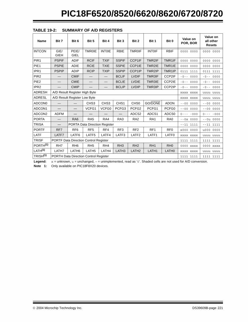
PIC18F6520/8520/6620/8620/6720/8720
TABLE 19-2: SUMMARY OF A/D REGISTERS
Name Bit 7 Bit 6 Bit 5 Bit 4 Bit 3 Bit 2 Bit 1 Bit 0Value on
POR, BOR
Value on all other Resets
INTCON GIE/GIEH
PEIE/GIEL
TMR0IE INT0IE RBIE TMR0IF INT0IF RBIF 0000 0000 0000 0000
PIR1 PSPIF ADIF RCIF TXIF SSPIF CCP1IF TMR2IF TMR1IF 0000 0000 0000 0000
PIE1 PSPIE ADIE RCIE TXIE SSPIE CCP1IE TMR2IE TMR1IE 0000 0000 0000 0000
IPR1 PSPIP ADIP RCIP TXIP SSPIP CCP1IP TMR2IP TMR1IP 0111 1111 0111 1111
PIR2 — CMIF — — BCLIF LVDIF TMR3IF CCP2IF -0-- 0000 -0-- 0000
PIE2 — CMIE — — BCLIE LVDIE TMR3IE CCP2IE -0-- 0000 -0-- 0000
IPR2 — CMIP — — BCLIP LVDIP TMR3IP CCP2IP -0-- 0000 -0-- 0000
ADRESH A/D Result Register High Byte xxxx xxxx uuuu uuuu
ADRESL A/D Result Register Low Byte xxxx xxxx uuuu uuuu
ADCON0 — — CHS3 CHS3 CHS1 CHS0 GO/DONE ADON --00 0000 --00 0000
ADCON1 — — VCFG1 VCFG0 PCFG3 PCFG2 PCFG1 PCFG0 --00 0000 --00 0000
ADCON2 ADFM — — — — ADCS2 ADCS1 ADCS0 0--- -000 0--- -000
PORTA — RA6 RA5 RA4 RA3 RA2 RA1 RA0 --0x 0000 --0u 0000
TRISA — PORTA Data Direction Register --11 1111 --11 1111
PORTF RF7 RF6 RF5 RF4 RF3 RF2 RF1 RF0 x000 0000 u000 0000
LATF LATF7 LATF6 LATF5 LATF4 LATF3 LATF2 LATF1 LATF0 xxxx xxxx uuuu uuuu
TRISF PORTF Data Direction Control Register 1111 1111 1111 1111
PORTH(1) RH7 RH6 RH5 RH4 RH3 RH2 RH1 RH0 0000 xxxx 0000 xxxx
LATH(1) LATH7 LATH6 LATH5 LATH4 LATH3 LATH2 LATH1 LATH0 xxxx xxxx uuuu uuuu
TRISH(1) PORTH Data Direction Control Register 1111 1111 1111 1111
Legend: x = unknown, u = unchanged, – = unimplemented, read as ‘0’. Shaded cells are not used for A/D conversion.Note 1: Only available on PIC18F8X20 devices.
2004 Microchip Technology Inc. DS39609B-page 221

PIC18F6520/8520/6620/8620/6720/8720
NOTES:
DS39609B-page 222 2004 Microchip Technology Inc.
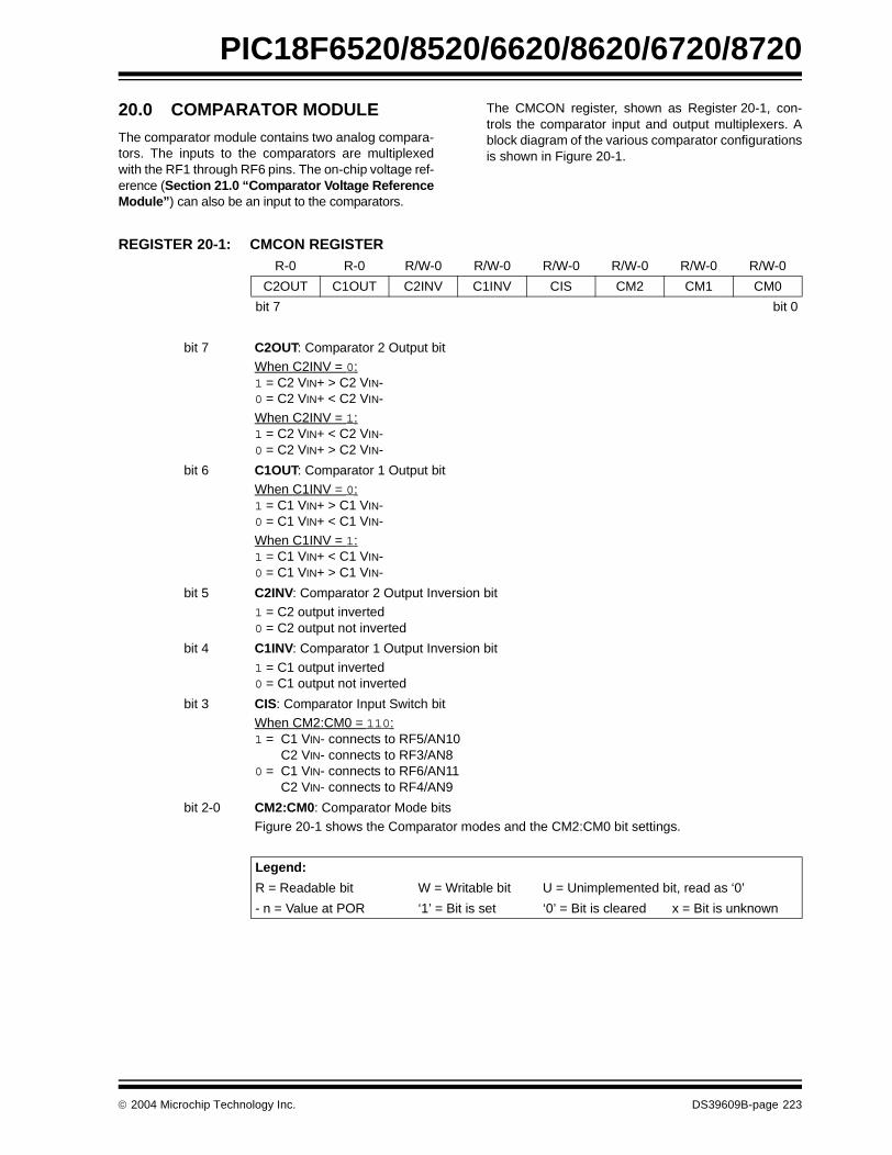
PIC18F6520/8520/6620/8620/6720/8720
20.0 COMPARATOR MODULE
The comparator module contains two analog compara-tors. The inputs to the comparators are multiplexedwith the RF1 through RF6 pins. The on-chip voltage ref-erence (Section 21.0 “Comparator Voltage ReferenceModule”) can also be an input to the comparators.
The CMCON register, shown as Register 20-1, con-trols the comparator input and output multiplexers. Ablock diagram of the various comparator configurationsis shown in Figure 20-1.
REGISTER 20-1: CMCON REGISTER R-0 R-0 R/W-0 R/W-0 R/W-0 R/W-0 R/W-0 R/W-0
C2OUT C1OUT C2INV C1INV CIS CM2 CM1 CM0
bit 7 bit 0
bit 7 C2OUT: Comparator 2 Output bitWhen C2INV = 0:1 = C2 VIN+ > C2 VIN-0 = C2 VIN+ < C2 VIN-
When C2INV = 1:1 = C2 VIN+ < C2 VIN-0 = C2 VIN+ > C2 VIN-
bit 6 C1OUT: Comparator 1 Output bitWhen C1INV = 0:1 = C1 VIN+ > C1 VIN-0 = C1 VIN+ < C1 VIN-
When C1INV = 1:1 = C1 VIN+ < C1 VIN-0 = C1 VIN+ > C1 VIN-
bit 5 C2INV: Comparator 2 Output Inversion bit1 = C2 output inverted0 = C2 output not inverted
bit 4 C1INV: Comparator 1 Output Inversion bit
1 = C1 output inverted0 = C1 output not inverted
bit 3 CIS: Comparator Input Switch bitWhen CM2:CM0 = 110:1 = C1 VIN- connects to RF5/AN10
C2 VIN- connects to RF3/AN80 = C1 VIN- connects to RF6/AN11
C2 VIN- connects to RF4/AN9
bit 2-0 CM2:CM0: Comparator Mode bitsFigure 20-1 shows the Comparator modes and the CM2:CM0 bit settings.
Legend:
R = Readable bit W = Writable bit U = Unimplemented bit, read as ‘0’
- n = Value at POR ‘1’ = Bit is set ‘0’ = Bit is cleared x = Bit is unknown
2004 Microchip Technology Inc. DS39609B-page 223

PIC18F6520/8520/6620/8620/6720/8720
20.1 Comparator Configuration
There are eight modes of operation for the compara-tors. The CMCON register is used to select thesemodes. Figure 20-1 shows the eight possible modes.The TRISF register controls the data direction of thecomparator pins for each mode. If the Comparatormode is changed, the comparator output level may not
be valid for the specified mode change delay shown inthe Electrical Specifications (Section 26.0 “ElectricalCharacteristics”).
FIGURE 20-1: COMPARATOR I/O OPERATING MODES
Note: Comparator interrupts should be disabledduring a Comparator mode change.Otherwise, a false interrupt may occur.
C1RF6/AN11 VIN-
VIN+RF5/AN10Off (Read as ‘0’)
Comparators Reset (POR Default Value)
A
A
CM2:CM0 = 000
C2RF4/AN9 VIN-
VIN+RF3/AN8Off (Read as ‘0’)
A
A
C1RF6/AN11 VIN-
VIN+RF5/AN10C1OUT
Two Independent Comparators
A
A
CM2:CM0 = 010
C2RF4/AN9 VIN-
VIN+RF3/AN8C2OUT
A
A
C1RF6/AN11 VIN-
VIN+RF5/AN10C1OUT
Two Common Reference Comparators
A
A
CM2:CM0 = 100
C2RF4/AN9 VIN-
VIN+RF3/AN8C2OUT
A
D
C2RF4/AN9 VIN-
VIN+RF3/AN8Off (Read as ‘0’)
One Independent Comparator with Output
D
D
CM2:CM0 = 001
C1RF6/AN11 VIN-
VIN+RF5/AN10C1OUT
A
A
C1RF6/AN11 VIN-
VIN+RF5/AN10Off (Read as ‘0’)
Comparators Off
D
D
CM2:CM0 = 111
C2RF4/AN9 VIN-
VIN+RF3/AN8Off (Read as ‘0’)
D
D
C1
RF6/AN11 VIN-
VIN+RF5/AN10 C1OUT
Four Inputs Multiplexed to Two Comparators
A
A
CM2:CM0 = 110
C2
RF4/AN9 VIN-
VIN+RF3/AN8 C2OUT
A
A
From VREF Module
CIS = 0CIS = 1
CIS = 0CIS = 1
C1RF6/AN11 VIN-
VIN+RF5/AN10C1OUT
Two Common Reference Comparators with Outputs
A
A
CM2:CM0 = 101
C2RF4/AN9 VIN-
VIN+RF3/AN8C2OUT
A
D
A = Analog Input, port reads zeros always D = Digital Input CIS (CMCON<3>) is the Comparator Input Switch
CVREF
C1RF6/AN11 VIN-
VIN+RF5/AN10C1OUT
Two Independent Comparators with Outputs
A
A
CM2:CM0 = 011
C2RF4/AN9 VIN-
VIN+RF3/AN8C2OUT
A
A
RF2/AN7/C1OUT
RF1/AN6/C2OUT
RF2/AN7/C1OUT
RF1/AN6/C2OUT
RF2/AN7/C1OUT
DS39609B-page 224 2004 Microchip Technology Inc.

PIC18F6520/8520/6620/8620/6720/8720
20.2 Comparator Operation
A single comparator is shown in Figure 20-2, along withthe relationship between the analog input levels andthe digital output. When the analog input at VIN+ is lessthan the analog input VIN-, the output of the comparatoris a digital low level. When the analog input at VIN+ isgreater than the analog input VIN-, the output of thecomparator is a digital high level. The shaded areas ofthe output of the comparator in Figure 20-2 representthe uncertainty, due to input offsets and response time.
20.3 Comparator Reference
An external or internal reference signal may be used,depending on the comparator operating mode. Theanalog signal present at VIN- is compared to the signalat VIN+ and the digital output of the comparator isadjusted accordingly (Figure 20-2).
FIGURE 20-2: SINGLE COMPARATOR
20.3.1 EXTERNAL REFERENCE SIGNAL
When external voltage references are used, thecomparator module can be configured to have the com-parators operate from the same, or different referencesources. However, threshold detector applications mayrequire the same reference. The reference signal mustbe between VSS and VDD and can be applied to eitherpin of the comparator(s).
20.3.2 INTERNAL REFERENCE SIGNAL
The comparator module also allows the selection of aninternally generated voltage reference for the compara-tors. Section 21.0 “Comparator Voltage ReferenceModule” contains a detailed description of the compar-ator voltage reference module that provides this signal.The internal reference signal is used when comparatorsare in mode CM<2:0> = 110 (Figure 20-1). In thismode, the internal voltage reference is applied to theVIN+ pin of both comparators.
20.4 Comparator Response Time
Response time is the minimum time, after selecting anew reference voltage or input source, before the com-parator output has a valid level. If the internal referenceis changed, the maximum delay of the internal voltagereference must be considered when using the compar-ator outputs. Otherwise, the maximum delay of thecomparators should be used (Section 26.0 “ElectricalCharacteristics”).
20.5 Comparator Outputs
The comparator outputs are read through the CMCONregister. These bits are read-only. The comparatoroutputs may also be directly output to the RF1 and RF2I/O pins. When enabled, multiplexors in the output pathof the RF1 and RF2 pins will switch and the output ofeach pin will be the unsynchronized output of the com-parator. The uncertainty of each of the comparators isrelated to the input offset voltage and the response timegiven in the specifications. Figure 20-3 shows thecomparator output block diagram.
The TRISF bits will still function as an output enable/disable for the RF1 and RF2 pins while in this mode.
The polarity of the comparator outputs can be changedusing the C2INV and C1INV bits (CMCON<4:5>).
–
+VIN+
VIN-Output
VIN–
VIN+
OutputOutput
VIN+
VIN-
Note 1: When reading the port register, all pinsconfigured as analog inputs will read as a‘0’. Pins configured as digital inputs willconvert an analog input, according to theSchmitt Trigger input specification.
2: Analog levels on any pin defined as a dig-ital input may cause the input buffer toconsume more current than is specified.
2004 Microchip Technology Inc. DS39609B-page 225

PIC18F6520/8520/6620/8620/6720/8720
FIGURE 20-3: COMPARATOR OUTPUT BLOCK DIAGRAM
20.6 Comparator Interrupts
The comparator interrupt flag is set whenever there isa change in the output value of either comparator.Software will need to maintain information about thestatus of the output bits, as read from CMCON<7:6>, todetermine the actual change that occurred. The CMIFbit (PIR registers) is the Comparator Interrupt Flag. TheCMIF bit must be reset by clearing ‘0’. Since it is alsopossible to write a ‘1’ to this register, a simulatedinterrupt may be initiated.
The CMIE bit (PIE registers) and the PEIE bit (INTCONregister) must be set to enable the interrupt. In addition,the GIE bit must also be set. If any of these bits areclear, the interrupt is not enabled, though the CMIF bitwill still be set if an interrupt condition occurs.
The user, in the Interrupt Service Routine, can clear theinterrupt in the following manner:
a) Any read or write of CMCON will end themismatch condition.
b) Clear flag bit CMIF.
A mismatch condition will continue to set flag bit CMIF.Reading CMCON will end the mismatch condition andallow flag bit CMIF to be cleared.
DQ
EN
To RF1 orRF2 pin
BusData
Read CMCON
Set
MULTIPLEX
CMIFbit
-+
DQ
EN
CL
Port pins
Read CMCON
Reset
FromOtherComparator
CxINV
Note: If a change in the CMCON register(C1OUT or C2OUT) should occur when aread operation is being executed (start ofthe Q2 cycle), then the CMIF (PIRregisters) interrupt flag may not get set.
DS39609B-page 226 2004 Microchip Technology Inc.

PIC18F6520/8520/6620/8620/6720/8720
20.7 Comparator Operation During Sleep
When a comparator is active and the device is placedin Sleep mode, the comparator remains active and theinterrupt is functional, if enabled. This interrupt willwake-up the device from Sleep mode, when enabled.While the comparator is powered up, higher Sleepcurrents than shown in the power-down currentspecification will occur. Each operational comparatorwill consume additional current, as shown in the com-parator specifications. To minimize power consumptionwhile in Sleep mode, turn off the comparators(CM<2:0> = 111) before entering Sleep. If the devicewakes up from Sleep, the contents of the CMCONregister are not affected.
20.8 Effects of a Reset
A device Reset forces the CMCON register to its Resetstate, causing the comparator module to be in the Com-parator Reset mode, CM<2:0> = 000. This ensuresthat all potential inputs are analog inputs. Device cur-rent is minimized when analog inputs are present atReset time. The comparators will be powered downduring the Reset interval.
20.9 Analog Input ConnectionConsiderations
A simplified circuit for an analog input is shown inFigure 20-4. Since the analog pins are connected to adigital output, they have reverse biased diodes to VDD
and VSS. The analog input, therefore, must be betweenVSS and VDD. If the input voltage deviates from thisrange by more than 0.6V in either direction, one of thediodes is forward biased and a latch-up condition mayoccur. A maximum source impedance of 10 kΩ isrecommended for the analog sources. Any externalcomponent connected to an analog input pin, such asa capacitor or a Zener diode, should have very littleleakage current.
FIGURE 20-4: COMPARATOR ANALOG INPUT MODEL
VA
RS < 10k
AIN
CPIN5 pF
VDD
VT = 0.6V
VT = 0.6V
RIC
ILEAKAGE±500 nA
VSS
Legend: CPIN = Input CapacitanceVT = Threshold VoltageILEAKAGE = Leakage Current at the pin due to various junctionsRIC = Interconnect ResistanceRS = Source ImpedanceVA = Analog Voltage
ComparatorInput
2004 Microchip Technology Inc. DS39609B-page 227

PIC18F6520/8520/6620/8620/6720/8720
TABLE 20-1: REGISTERS ASSOCIATED WITH COMPARATOR MODULE
Name Bit 7 Bit 6 Bit 5 Bit 4 Bit 3 Bit 2 Bit 1 Bit 0Value on
POR
Value onall otherResets
CMCON C2OUT C1OUT C2INV C1INV CIS CM2 CM1 CM0 0000 0000 0000 0000
CVRCON CVREN CVROE CVRR CVRSS CVR3 CVR2 CVR1 CVR0 0000 0000 0000 0000
INTCON GIE/GIEH
PEIE/GIEL
TMR0IE INT0IE RBIE TMR0IF INT0IF RBIF 0000 0000 0000 0000
PIR2 — CMIF — — BCLIF LVDIF TMR3IF CCP2IF -0-- 0000 -0-- 0000
PIE2 — CMIE — — BCLIE LVDIE TMR3IE CCP2IE -0-- 0000 -0-- 0000
IPR2 — CMIP — — BCLIP LVDIP TMR3IP CCP2IP -1-- 1111 -1-- 1111
PORTF RF7 RF6 RF5 RF4 RF3 RF2 RF1 RF0 x000 0000 u000 0000
LATF LATF7 LATF6 LATF5 LATF4 LATF3 LATF2 LATF1 LATF0 xxxx xxxx uuuu uuuu
TRISF TRISF7 TRISF6 TRISF5 TRISF4 TRISF3 TRISF2 TRISF1 TRISF0 1111 1111 1111 1111
Legend: x = unknown, u = unchanged, – = unimplemented, read as ‘0’.Shaded cells are unused by the comparator module.
DS39609B-page 228 2004 Microchip Technology Inc.

PIC18F6520/8520/6620/8620/6720/8720
21.0 COMPARATOR VOLTAGE REFERENCE MODULE
The comparator voltage reference is a 16-tap resistorladder network that provides a selectable voltage refer-ence. The resistor ladder is segmented to provide tworanges of CVREF values and has a power-down functionto conserve power when the reference is not being used.The CVRCON register controls the operation of thereference as shown in Register 21-1. The block diagramis given in Figure 21-1.
The comparator reference supply voltage can comefrom either VDD or VSS, or the external VREF+ andVREF- that are multiplexed with RA3 and RA2. Thecomparator reference supply voltage is controlled bythe CVRSS bit.
21.1 Configuring the Comparator Voltage Reference
The comparator voltage reference can output 16 distinctvoltage levels for each range. The equations used tocalculate the output of the comparator voltage referenceare as follows:
If CVRR = 1: CVREF = (CVR<3:0>/24) x CVRSRC
If CVRR = 0: CVREF = (CVRSRC x 1/4) + (CVR<3:0>/32) x CVRSRC
The settling time of the comparator voltage referencemust be considered when changing the CVREF output(Section 26.0 “Electrical Characteristics”).
REGISTER 21-1: CVRCON REGISTER
Note: In order to select external VREF+ and VREF-supply voltages, the Voltage Reference Con-figuration bits (VCFG1:VCFG0) of theADCON1 register must be set appropriately.
R/W-0 R/W-0 R/W-0 R/W-0 R/W-0 R/W-0 R/W-0 R/W-0
CVREN CVROE CVRR CVRSS CVR3 CVR2 CVR1 CVR0
bit 7 bit 0
bit 7 CVREN: Comparator Voltage Reference Enable bit1 = CVREF circuit powered on 0 = CVREF circuit powered down
bit 6 CVROE: Comparator VREF Output Enable bit(1)
1 = CVREF voltage level is also output on the RF5/AN10/CVREF pin 0 = CVREF voltage is disconnected from the RF5/AN10/CVREF pin
bit 5 CVRR: Comparator VREF Range Selection bit1 = 0.00 CVRSRC to 0.667 CVRSRC, with CVRSRC/24 step size (low range) 0 = 0.25 CVRSRC to 0.75 CVRSRC, with CVRSRC/32 step size (high range)
bit 4 CVRSS: Comparator VREF Source Selection bit(2)
1 = Comparator reference source CVRSRC = VREF+ – VREF-0 = Comparator reference source CVRSRC = VDD – VSS
bit 3-0 CVR3:CVR0: Comparator VREF Value Selection bits (0 ≤ VR3:VR0 ≤ 15)
When CVRR = 1: CVREF = (CVR<3:0>/24) • (CVRSRC)
When CVRR = 0: CVREF = 1/4 • (CVRSRC) + (CVR3:CVR0/32) • (CVRSRC)
Note 1: If enabled for output, RF5 must also be configured as an input by setting TRISF<5>to ‘1’.
2: In order to select external VREF+ and VREF- supply voltages, the VoltageReference Configuration bits (VCFG1:VCFG0) of the ADCON1 register must beset appropriately.
Legend:
R = Readable bit W = Writable bit U = Unimplemented bit, read as ‘0’
- n = Value at POR ‘1’ = Bit is set ‘0’ = Bit is cleared x = Bit is unknown
2004 Microchip Technology Inc. DS39609B-page 229

PIC18F6520/8520/6620/8620/6720/8720
FIGURE 21-1: VOLTAGE REFERENCE BLOCK DIAGRAM
21.2 Voltage Reference Accuracy/Error
The full range of voltage reference cannot be realizeddue to the construction of the module. The transistorson the top and bottom of the resistor ladder network(Figure 21-1) keep CVREF from approaching the refer-ence source rails. The voltage reference is derivedfrom the reference source; therefore, the CVREF outputchanges with fluctuations in that source. The testedabsolute accuracy of the voltage reference can befound in Section 26.0 “Electrical Characteristics”.
21.3 Operation During Sleep
When the device wakes up from Sleep through aninterrupt or a Watchdog Timer time-out, the contents ofthe CVRCON register are not affected. To minimizecurrent consumption in Sleep mode, the voltagereference should be disabled.
21.4 Effects of a Reset
A device Reset disables the voltage reference byclearing bit CVREN (CVRCON<7>). This Reset alsodisconnects the reference from the RA2 pin by clearingbit CVROE (CVRCON<6>) and selects the high-voltage range by clearing bit CVRR (CVRCON<5>).The VRSS value select bits, CVRCON<3:0>, are alsocleared.
21.5 Connection Considerations
The voltage reference module operates independentlyof the comparator module. The output of the referencegenerator may be connected to the RF5 pin if theTRISF<5> bit is set and the CVROE bit is set. Enablingthe voltage reference output onto the RF5 pin,configured as a digital input, will increase currentconsumption. Connecting RF5 as a digital output withVRSS enabled will also increase current consumption.
The RF5 pin can be used as a simple D/A output withlimited drive capability. Due to the limited current drivecapability, a buffer must be used on the voltage refer-ence output for external connections to VREF.Figure 21-2 shows an example buffering technique.
Note: R is defined in Section 26.0 “Electrical Characteristics”.
CVRR8R
CVR3
CVR0(From CVRCON<3:0>)16-1 Analog Mux
8R R R R RCVREN
CVREF
16 StagesCVRSS = 0
VDD VREF+
CVRSS = 0
CVRSS = 1
VREF-
CVRSS = 1
DS39609B-page 230 2004 Microchip Technology Inc.

PIC18F6520/8520/6620/8620/6720/8720
FIGURE 21-2: VOLTAGE REFERENCE OUTPUT BUFFER EXAMPLE
TABLE 21-1: REGISTERS ASSOCIATED WITH COMPARATOR VOLTAGE REFERENCE
CVREF Output+–
CVREF
Module
Voltage Reference
Output Impedance
R(1) RF5
Note 1: R is dependent upon the Comparator Voltage Reference Configuration bits CVRCON<3:0> and CVRCON<5>.
Name Bit 7 Bit 6 Bit 5 Bit 4 Bit 3 Bit 2 Bit 1 Bit 0Value on
POR
Value onall otherResets
CVRCON CVREN CVROE CVRR CVRSS CVR3 CVR2 CVR1 CVR0 0000 0000 0000 0000
CMCON C2OUT C1OUT C2INV C1INV CIS CM2 CM1 CM0 0000 0000 0000 0000
TRISF TRISF7 TRISF6 TRISF5 TRISF4 TRISF3 TRISF2 TRISF1 TRISF0 1111 1111 1111 1111
Legend: x = unknown, u = unchanged, – = unimplemented, read as ‘0’. Shaded cells are not used with the comparator voltage reference.
2004 Microchip Technology Inc. DS39609B-page 231

PIC18F6520/8520/6620/8620/6720/8720
NOTES:
DS39609B-page 232 2004 Microchip Technology Inc.
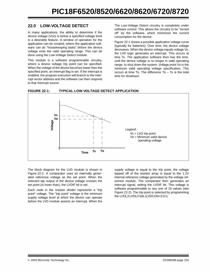
PIC18F6520/8520/6620/8620/6720/8720
22.0 LOW-VOLTAGE DETECT
In many applications, the ability to determine if thedevice voltage (VDD) is below a specified voltage levelis a desirable feature. A window of operation for theapplication can be created, where the application soft-ware can do “housekeeping tasks” before the devicevoltage exits the valid operating range. This can bedone using the Low-Voltage Detect module.
This module is a software programmable circuitry,where a device voltage trip point can be specified.When the voltage of the device becomes lower then thespecified point, an interrupt flag is set. If the interrupt isenabled, the program execution will branch to the inter-rupt vector address and the software can then respondto that interrupt source.
The Low-Voltage Detect circuitry is completely undersoftware control. This allows the circuitry to be “turnedoff” by the software, which minimizes the currentconsumption for the device.
Figure 22-1 shows a possible application voltage curve(typically for batteries). Over time, the device voltagedecreases. When the device voltage equals voltage VA,the LVD logic generates an interrupt. This occurs attime TA. The application software then has the time,until the device voltage is no longer in valid operatingrange, to shut down the system. Voltage point VB is theminimum valid operating voltage specification. Thisoccurs at time TB. The difference TB – TA is the totaltime for shutdown.
FIGURE 22-1: TYPICAL LOW-VOLTAGE DETECT APPLICATION
The block diagram for the LVD module is shown inFigure 22-2. A comparator uses an internally gener-ated reference voltage as the set point. When theselected tap output of the device voltage crosses theset point (is lower than), the LVDIF bit is set.
Each node in the resistor divider represents a “trippoint” voltage. The “trip point” voltage is the minimumsupply voltage level at which the device can operatebefore the LVD module asserts an interrupt. When the
supply voltage is equal to the trip point, the voltagetapped off of the resistor array is equal to the 1.2Vinternal reference voltage generated by the voltage ref-erence module. The comparator then generates aninterrupt signal, setting the LVDIF bit. This voltage issoftware programmable to any one of 16 values (seeFigure 22-2). The trip point is selected by programmingthe LVDL3:LVDL0 bits (LVDCON<3:0>).
Time
Volta
ge
VAVB
TA TB
VA = LVD trip pointVB = Minimum valid device operating voltage
Legend:
2004 Microchip Technology Inc. DS39609B-page 233
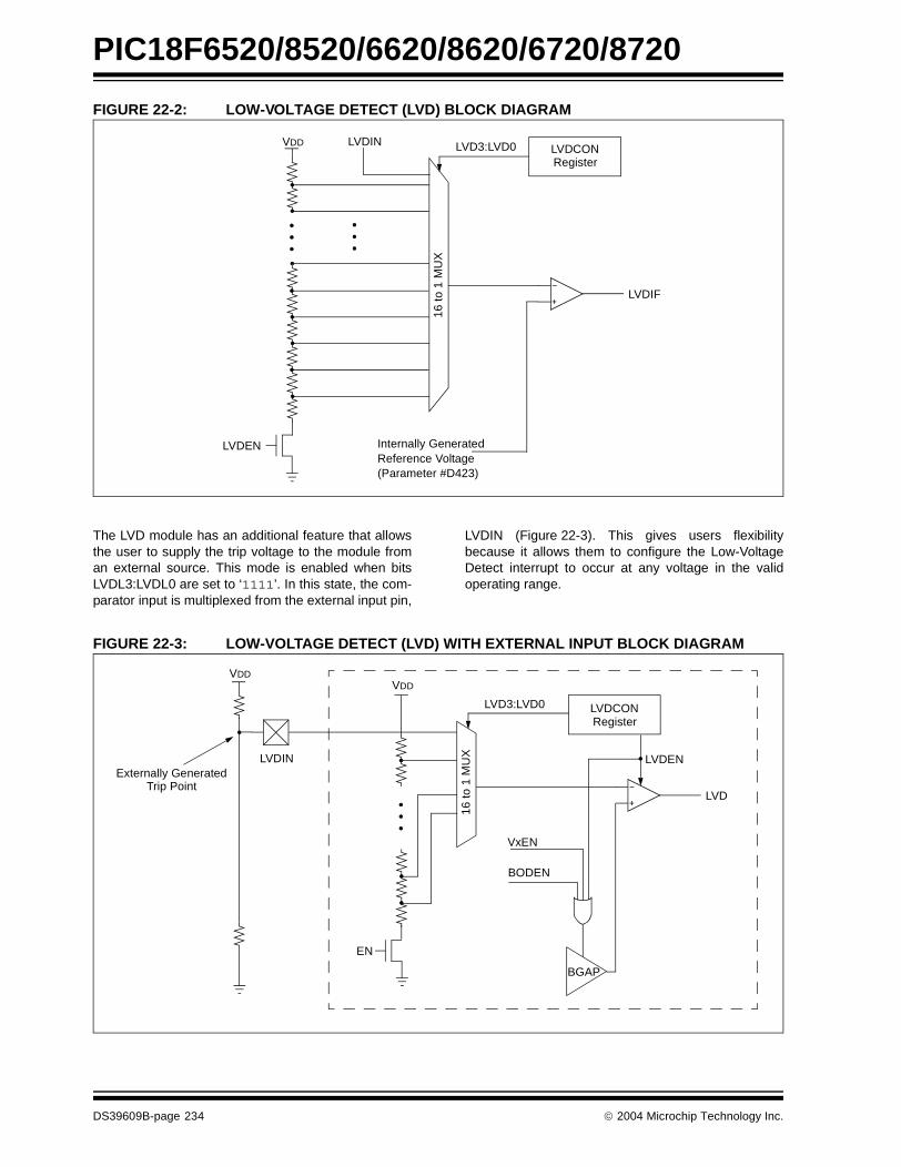
PIC18F6520/8520/6620/8620/6720/8720
FIGURE 22-2: LOW-VOLTAGE DETECT (LVD) BLOCK DIAGRAM
The LVD module has an additional feature that allowsthe user to supply the trip voltage to the module froman external source. This mode is enabled when bitsLVDL3:LVDL0 are set to ‘1111’. In this state, the com-parator input is multiplexed from the external input pin,
LVDIN (Figure 22-3). This gives users flexibilitybecause it allows them to configure the Low-VoltageDetect interrupt to occur at any voltage in the validoperating range.
FIGURE 22-3: LOW-VOLTAGE DETECT (LVD) WITH EXTERNAL INPUT BLOCK DIAGRAM
LVDIF
VDD
16 to
1 M
UX
LVDEN
LVDCON
Internally GeneratedReference Voltage
LVDIN
(Parameter #D423)
LVD3:LVD0Register
LVD
EN
16 to
1 M
UX
BGAP
BODEN
LVDEN
VxEN
LVDIN
VDDVDD
Externally GeneratedTrip Point
LVD3:LVD0 LVDCONRegister
DS39609B-page 234 2004 Microchip Technology Inc.

PIC18F6520/8520/6620/8620/6720/8720
22.1 Control Register
The Low-Voltage Detect Control register controls theoperation of the Low-Voltage Detect circuitry.
REGISTER 22-1: LVDCON REGISTER U-0 U-0 R-0 R/W-0 R/W-0 R/W-1 R/W-0 R/W-1
— — IRVST LVDEN LVDL3 LVDL2 LVDL1 LVDL0
bit 7 bit 0
bit 7-6 Unimplemented: Read as ‘0’
bit 5 IRVST: Internal Reference Voltage Stable Flag bit1 = Indicates that the Low-Voltage Detect logic will generate the interrupt flag at the specified
voltage range0 = Indicates that the Low-Voltage Detect logic will not generate the interrupt flag at the
specified voltage range and the LVD interrupt should not be enabled
bit 4 LVDEN: Low-Voltage Detect Power Enable bit1 = Enables LVD, powers up LVD circuit 0 = Disables LVD, powers down LVD circuit
bit 3-0 LVDL3:LVDL0: Low-Voltage Detection Limit bits(2)
1111 = External analog input is used (input comes from the LVDIN pin) 1110 = 4.64V1101 = 4.33V1100 = 4.13V1011 = 3.92V1010 = 3.72V 1001 = 3.61V1000 = 3.41V0111 = 3.1V0110 = 2.89V0101 = 2.78V0100 = 2.58V0011 = 2.47V0010 = 2.27V0001 = 2.06V0000 = Reserved
Note 1: LVDL3:LVDL0 modes which result in a trip point below the valid operating voltageof the device are not tested.
2: Typical values shown, see parameter D420 in Table 26-3 for more information.
Legend:
R = Readable bit W = Writable bit U = Unimplemented bit, read as ‘0’
- n = Value at POR ‘1’ = Bit is set ‘0’ = Bit is cleared x = Bit is unknown
2004 Microchip Technology Inc. DS39609B-page 235

PIC18F6520/8520/6620/8620/6720/8720
22.2 Operation
Depending on the power source for the device voltage,the voltage normally decreases relatively slowly. Thismeans that the LVD module does not need to be con-stantly operating. To decrease the current require-ments, the LVD circuitry only needs to be enabled forshort periods, where the voltage is checked. Afterdoing the check, the LVD module may be disabled.
Each time that the LVD module is enabled, the circuitryrequires some time to stabilize. After the circuitry hasstabilized, all status flags may be cleared. The modulewill then indicate the proper state of the system.
The following steps are needed to set up the LVDmodule:
1. Write the value to the LVDL3:LVDL0 bits(LVDCON register), which selects the desiredLVD trip point.
2. Ensure that LVD interrupts are disabled (theLVDIE bit is cleared or the GIE bit is cleared).
3. Enable the LVD module (set the LVDEN bit inthe LVDCON register).
4. Wait for the LVD module to stabilize (the IRVSTbit to become set).
5. Clear the LVD interrupt flag, which may havefalsely become set, until the LVD module hasstabilized (clear the LVDIF bit).
6. Enable the LVD interrupt (set the LVDIE and theGIE bits).
Figure 22-4 shows typical waveforms that the LVDmodule may be used to detect.
FIGURE 22-4: LOW-VOLTAGE DETECT WAVEFORMS
VLVD
VDD
LVDIF
VLVD
VDD
Enable LVD
Internally Generated TIVRST
LVDIF may not be set
Enable LVD
LVDIF
LVDIF cleared in software
LVDIF cleared in software
LVDIF cleared in software,
CASE 1:
CASE 2:
LVDIF remains set since LVD condition still exists
Reference Stable
Internally GeneratedReference Stable
TIVRST
DS39609B-page 236 2004 Microchip Technology Inc.
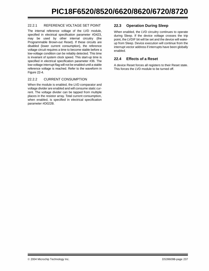
PIC18F6520/8520/6620/8620/6720/8720
22.2.1 REFERENCE VOLTAGE SET POINT
The internal reference voltage of the LVD module,specified in electrical specification parameter #D423,may be used by other internal circuitry (theProgrammable Brown-out Reset). If these circuits aredisabled (lower current consumption), the referencevoltage circuit requires a time to become stable before alow-voltage condition can be reliably detected. This timeis invariant of system clock speed. This start-up time isspecified in electrical specification parameter #36. Thelow-voltage interrupt flag will not be enabled until a stablereference voltage is reached. Refer to the waveform inFigure 22-4.
22.2.2 CURRENT CONSUMPTION
When the module is enabled, the LVD comparator andvoltage divider are enabled and will consume static cur-rent. The voltage divider can be tapped from multipleplaces in the resistor array. Total current consumption,when enabled, is specified in electrical specificationparameter #D022B.
22.3 Operation During Sleep
When enabled, the LVD circuitry continues to operateduring Sleep. If the device voltage crosses the trippoint, the LVDIF bit will be set and the device will wake-up from Sleep. Device execution will continue from theinterrupt vector address if interrupts have been globallyenabled.
22.4 Effects of a Reset
A device Reset forces all registers to their Reset state.This forces the LVD module to be turned off.
2004 Microchip Technology Inc. DS39609B-page 237

PIC18F6520/8520/6620/8620/6720/8720
NOTES:
DS39609B-page 238 2004 Microchip Technology Inc.

PIC18F6520/8520/6620/8620/6720/8720
23.0 SPECIAL FEATURES OF THE CPU
There are several features intended to maximize sys-tem reliability, minimize cost through elimination ofexternal components, provide power saving operatingmodes and offer code protection. These are:
• Oscillator Selection
• Reset- Power-on Reset (POR)- Power-up Timer (PWRT)
- Oscillator Start-up Timer (OST)- Brown-out Reset (BOR)
• Interrupts
• Watchdog Timer (WDT)• Sleep• Code Protection
• ID Locations• In-Circuit Serial Programming
All PIC18FXX20 devices have a Watchdog Timer,which is permanently enabled via the configuration bits,or software controlled. It runs off its own RC oscillatorfor added reliability. There are two timers that offernecessary delays on power-up. One is the OscillatorStart-up Timer (OST), intended to keep the chip inReset until the crystal oscillator is stable. The other isthe Power-up Timer (PWRT), which provides a fixeddelay on power-up only, designed to keep the part inReset while the power supply stabilizes. With these twotimers on-chip, most applications need no externalReset circuitry.
Sleep mode is designed to offer a very low currentpower-down mode. The user can wake-up from Sleepthrough external Reset, Watchdog Timer Wake-up orthrough an interrupt. Several oscillator options are alsomade available to allow the part to fit the application.The RC oscillator option saves system cost, while theLP crystal option saves power. A set of configurationbits is used to select various options.
23.1 Configuration Bits
The configuration bits can be programmed (read as‘0’), or left unprogrammed (read as ‘1’), to select vari-ous device configurations. These bits are mapped,starting at program memory location 300000h.
The user will note that address 300000h is beyond theuser program memory space. In fact, it belongs to theconfiguration memory space (300000h through3FFFFFh), which can only be accessed using tablereads and table writes.
Programming the configuration registers is done in amanner similar to programming the Flash memory. TheEECON1 register WR bit starts a self-timed write to theconfiguration register. In normal operation mode, aTBLWT instruction with the TBLPTR pointed to theconfiguration register sets up the address and the datafor the configuration register write. Setting the WR bitstarts a long write to the configuration register. Theconfiguration registers are written a byte at a time. Towrite or erase a configuration cell, a TBLWT instructioncan write a ‘1’ or a ‘0’ into the cell.
2004 Microchip Technology Inc. DS39609B-page 239

PIC18F6520/8520/6620/8620/6720/8720
TABLE 23-1: CONFIGURATION BITS AND DEVICE IDS
REGISTER 23-1: CONFIG1H: CONFIGURATION REGISTER 1 HIGH (BYTE ADDRESS 300001h)
File Name Bit 7 Bit 6 Bit 5 Bit 4 Bit 3 Bit 2 Bit 1 Bit 0Default/
UnprogrammedValue
300001h CONFIG1H — — OSCSEN — — FOSC2 FOSC1 FOSC0 --1- -111
300002h CONFIG2L — — — — BORV1 BORV0 BODEN PWRTEN ---- 1111
300003h CONFIG2H — — — — WDTPS2 WDTPS1 WDTPS0 WDTEN ---- 1111
300004h(1) CONFIG3L WAIT — — — — — PM1 PM0 1--- --11
300005h CONFIG3H — — — — — — r(3) CCP2MX ---- --11
300006h CONFIG4L DEBUG — — — — LVP — STVREN 1--- -1-1
300008h CONFIG5L CP7(2) CP6(2) CP5(2) CP4(2) CP3 CP2 CP1 CP0 1111 1111
300009h CONFIG5H CPD CPB — — — — — — 11-- ----
30000Ah CONFIG6L WRT7(2) WRT6(2) WRT5(2) WRT4(2) WRT3 WRT2 WRT1 WRT0 1111 1111
30000Bh CONFIG6H WRTD WRTB WRTC — — — — — 111- ----
30000Ch CONFIG7L EBTR7(2) EBTR6(2) EBTR5(2) EBTR4(2) EBTR3 EBTR2 EBTR1 EBTR0 1111 1111
30000Dh CONFIG7H — EBTRB — — — — — — -1-- ----
3FFFFEh DEVID1 DEV2 DEV1 DEV0 REV4 REV3 REV2 REV1 REV0 (4)
3FFFFFh DEVID2 DEV10 DEV9 DEV8 DEV7 DEV6 DEV5 DEV4 DEV3 0000 0110
Legend: x = unknown, u = unchanged, – = unimplemented, q = value depends on condition, r = reserved. Shaded cells are unimplemented, read as ‘0’.
Note 1: Unimplemented in PIC18F6X20 devices; maintain this bit set.2: Unimplemented in PIC18FX520 and PIC18FX620 devices; maintain this bit set.3: Unimplemented in PIC18FX620 and PIC18FX720 devices; maintain this bit set.4: See Register 23-13 for DEVID1 values.
U-0 U-0 R/P-1 U-0 U-0 R/P-1 R/P-1 R/P-1
— — OSCSEN — — FOSC2 FOSC1 FOSC0
bit 7 bit 0
bit 7-6 Unimplemented: Read as ‘0’
bit 5 OSCSEN: Oscillator System Clock Switch Enable bit1 = Oscillator system clock switch option is disabled (main oscillator is source)0 = Timer1 Oscillator system clock switch option is enabled (oscillator switching is enabled)
bit 4-3 Unimplemented: Read as ‘0’
bit 2-0 FOSC2:FOSC0: Oscillator Selection bits111 = RC oscillator w/ OSC2 configured as RA6 110 = HS oscillator with PLL enabled; clock frequency = (4 x FOSC) 101 = EC oscillator w/ OSC2 configured as RA6 100 = EC oscillator w/ OSC2 configured as divide-by-4 clock output 011 = RC oscillator w/ OSC2 configured as divide-by-4 clock output010 = HS oscillator 001 = XT oscillator 000 = LP oscillator
Legend:
R = Readable bit P = Programmable bit U = Unimplemented bit, read as ‘0’
- n = Value when device is unprogrammed u = Unchanged from programmed state
DS39609B-page 240 2004 Microchip Technology Inc.

PIC18F6520/8520/6620/8620/6720/8720
REGISTER 23-2: CONFIG2L: CONFIGURATION REGISTER 2 LOW (BYTE ADDRESS 300002h)
REGISTER 23-3: CONFIG2H: CONFIGURATION REGISTER 2 HIGH (BYTE ADDRESS 300003h)
U-0 U-0 U-0 U-0 R/P-1 R/P-1 R/P-1 R/P-1
— — — — BORV1 BORV0 BOREN PWRTEN
bit 7 bit 0
bit 7-4 Unimplemented: Read as ‘0’
bit 3-2 BORV1:BORV0: Brown-out Reset Voltage bits11 = VBOR set to 2.5V 10 = VBOR set to 2.7V 01 = VBOR set to 4.2V 00 = VBOR set to 4.5V
bit 1 BOREN: Brown-out Reset Enable bit1 = Brown-out Reset enabled 0 = Brown-out Reset disabled
bit 0 PWRTEN: Power-up Timer Enable bit
1 = PWRT disabled 0 = PWRT enabled
Legend:
R = Readable bit P = Programmable bit U = Unimplemented bit, read as ‘0’
- n = Value when device is unprogrammed u = Unchanged from programmed state
U-0 U-0 U-0 U-0 R/P-1 R/P-1 R/P-1 R/P-1
— — — — WDTPS2 WDTPS1 WDTPS0 WDTEN
bit 7 bit 0
bit 7-4 Unimplemented: Read as ‘0’
bit 3-1 WDTPS2:WDTPS0: Watchdog Timer Postscale Select bits
111 = 1:128 110 = 1:64101 = 1:32 100 = 1:16011 = 1:8 010 = 1:4 001 = 1:2 000 = 1:1
bit 0 WDTEN: Watchdog Timer Enable bit
1 = WDT enabled 0 = WDT disabled (control is placed on the SWDTEN bit)
Legend:
R = Readable bit P = Programmable bit U = Unimplemented bit, read as ‘0’
- n = Value when device is unprogrammed u = Unchanged from programmed state
2004 Microchip Technology Inc. DS39609B-page 241

PIC18F6520/8520/6620/8620/6720/8720
REGISTER 23-4: CONFIG3L: CONFIGURATION REGISTER 3 LOW (BYTE ADDRESS 300004h)(1)
REGISTER 23-5: CONFIG3H: CONFIGURATION REGISTER 3 HIGH (BYTE ADDRESS 300005h)
R/P-1 U-0 U-0 U-0 U-0 U-0 R/P-1 R/P-1
WAIT — — — — — PM1 PM0
bit 7 bit 0
bit 7 WAIT: External Bus Data Wait Enable bit
1 = Wait selections unavailable for table reads and table writes 0 = Wait selections for table reads and table writes are determined by the WAIT1:WAIT0 bits
(MEMCOM<5:4>)
bit 6-2 Unimplemented: Read as ‘0’
bit 1-0 PM1:PM0: Processor Mode Select bits
11 = Microcontroller mode 10 = Microprocessor mode 01 = Microprocessor with Boot Block mode 00 = Extended Microcontroller mode
Note 1: This register is unimplemented in PIC18F6X20 devices; maintain these bits set.
Legend:
R = Readable bit P = Programmable bit U = Unimplemented bit, read as ‘0’
- n = Value when device is unprogrammed u = Unchanged from programmed state
U-0 U-0 U-0 U-0 U-0 U-0 R/P-1 R/P-1
— — — — — — r(1) CCP2MX
bit 7 bit 0
bit 7-2 Unimplemented: Read as ‘0’
bit 1 Reserved: Read as unknown(1)
bit 0 CCP2MX: CCP2 Mux bit
In Microcontroller mode:1 = CCP2 input/output is multiplexed with RC1 0 = CCP2 input/output is multiplexed with RE7 In Microprocessor, Microprocessor with Boot Block and Extended Microcontroller modes(PIC18F8X20 devices only):1 = CCP2 input/output is multiplexed with RC1 0 = CCP2 input/output is multiplexed with RB3
Note 1: Unimplemented in PIC18FX620 and PIC18FX720 devices; read as ‘0’.
Legend:
R = Readable bit P = Programmable bit U = Unimplemented bit, read as ‘0’
- n = Value when device is unprogrammed u = Unchanged from programmed state
DS39609B-page 242 2004 Microchip Technology Inc.

PIC18F6520/8520/6620/8620/6720/8720
REGISTER 23-6: CONFIG4L: CONFIGURATION REGISTER 4 LOW (BYTE ADDRESS 300006h) R/P-1 U-0 U-0 U-0 U-0 R/P-1 U-0 R/P-1
DEBUG — — — — LVP — STVREN
bit 7 bit 0
bit 7 DEBUG: Background Debugger Enable bit1 = Background debugger disabled. RB6 and RB7 configured as general purpose I/O pins. 0 = Background debugger enabled. RB6 and RB7 are dedicated to In-Circuit Debug.
bit 6-3 Unimplemented: Read as ‘0’
bit 2 LVP: Low-Voltage ICSP Enable bit
1 = Low-voltage ICSP enabled 0 = Low-voltage ICSP disabled
bit 1 Unimplemented: Read as ‘0’
bit 0 STVREN: Stack Full/Underflow Reset Enable bit1 = Stack full/underflow will cause Reset 0 = Stack full/underflow will not cause Reset
Legend:
R = Readable bit P = Programmable bit U = Unimplemented bit, read as ‘0’
- n = Value when device is unprogrammed u = Unchanged from programmed state
2004 Microchip Technology Inc. DS39609B-page 243

PIC18F6520/8520/6620/8620/6720/8720
REGISTER 23-7: CONFIG5L: CONFIGURATION REGISTER 5 LOW (BYTE ADDRESS 300008h)
R/P-1 R/P-1 R/P-1 R/P-1 R/P-1 R/P-1 R/P-1 R/P-1
CP7(1) CP6(1) CP5(1) CP4(1) CP3 CP2 CP1 CP0
bit 7 bit 0
bit 7 CP7: Code Protection bit(1)
1 = Block 7 (01C000-01FFFFh) not code-protected 0 = Block 7 (01C000-01FFFFh) code-protected
bit 6 CP6: Code Protection bit(1)
1 = Block 6 (018000-01BFFFh) not code-protected 0 = Block 6 (018000-01BFFFh) code-protected
bit 5 CP5: Code Protection bit(1)
1 = Block 5 (014000-017FFFh) not code-protected 0 = Block 5 (014000-017FFFh) code-protected
bit 4 CP4: Code Protection bit(1)
1 = Block 4 (010000-013FFFh) not code-protected 0 = Block 4 (010000-013FFFh) code-protected
bit 3 CP3: Code Protection bit
For PIC18FX520 devices:1 = Block 3 (006000-007FFFh) not code-protected 0 = Block 3 (006000-007FFFh) code-protected For PIC18FX620 and PIC18FX720 devices:1 = Block 3 (00C000-00FFFFh) not code-protected 0 = Block 3 (00C000-00FFFFh) code-protected
bit 2 CP2: Code Protection bitFor PIC18FX520 devices:1 = Block 2 (004000-005FFFh) not code-protected 0 = Block 2 (004000-005FFFh) code-protected For PIC18FX620 and PIC18FX720 devices:1 = Block 2 (008000-00BFFFh) not code-protected 0 = Block 2 (008000-00BFFFh) code-protected
bit 1 CP1: Code Protection bitFor PIC18FX520 devices:1 = Block 1 (002000-003FFFh) not code-protected 0 = Block 1 (002000-003FFFh) code-protected
For PIC18FX620 and PIC18FX720 devices:1 = Block 1 (004000-007FFFh) not code-protected 0 = Block 1 (004000-007FFFh) code-protected
bit 0 CP0: Code Protection bit
For PIC18FX520 devices:1 = Block 0 (000800-001FFFh) not code-protected 0 = Block 0 (000800-001FFFh) code-protected For PIC18FX620 and PIC18FX720 devices:1 = Block 0 (000200-003FFFh) not code-protected 0 = Block 0 (000200-003FFFh) code-protected
Note 1: Unimplemented in PIC18FX520 and PIC18FX620 devices; maintain this bit set.
Legend:R = Readable bit P = Programmable bit U = Unimplemented bit, read as ‘0’
- n = Value when device is unprogrammed u = Unchanged from programmed state
DS39609B-page 244 2004 Microchip Technology Inc.

PIC18F6520/8520/6620/8620/6720/8720
REGISTER 23-8: CONFIG5H: CONFIGURATION REGISTER 5 HIGH (BYTE ADDRESS 300009h) R/C-1 R/C-1 U-0 U-0 U-0 U-0 U-0 U-0CPD CPB — — — — — —
bit 7 bit 0
bit 7 CPD: Data EEPROM Code Protection bit1 = Data EEPROM not code-protected0 = Data EEPROM code-protected
bit 6 CPB: Boot Block Code Protection bit
For PIC18FX520 devices:1 = Boot Block (000000-0007FFh) not code-protected0 = Boot Block (000000-0007FFh) code-protectedFor PIC18FX620 and PIC18FX720 devices:1 = Boot Block (000000-0001FFh) not code-protected0 = Boot Block (000000-0001FFh) code-protected
bit 5-0 Unimplemented: Read as ‘0’
Legend:R = Readable bit C = Clearable bit U = Unimplemented bit, read as ‘0’- n = Value when device is unprogrammed u = Unchanged from programmed state
2004 Microchip Technology Inc. DS39609B-page 245

PIC18F6520/8520/6620/8620/6720/8720
REGISTER 23-9: CONFIG6L: CONFIGURATION REGISTER 6 LOW (BYTE ADDRESS 30000Ah) R/P-1 R/P-1 R/P-1 R/P-1 R/P-1 R/P-1 R/P-1 R/P-1
WRT7(1) WRT6(1) WRT5(1) WRT4(1) WRT3 WRT2 WRT1 WRT0
bit 7 bit 0
bit 7 WR7: Write Protection bit(1)
1 = Block 7 (01C000-01FFFFh) not write-protected 0 = Block 7 (01C000-01FFFFh) write-protected
bit 6 WR6: Write Protection bit(1)
1 = Block 6 (018000-01BFFFh) not write-protected 0 = Block 6 (018000-01BFFFh) write-protected
bit 5 WR5: Write Protection bit(1)
1 = Block 5 (014000-017FFFh) not write-protected 0 = Block 5 (014000-017FFFh) write-protected
bit 4 WR4: Write Protection bit(1)
1 = Block 4 (010000-013FFFh) not write-protected 0 = Block 4 (010000-013FFFh) write-protected
bit 3 WR3: Write Protection bit
For PIC18FX520 devices:1 = Block 3 (006000-007FFFh) not write-protected 0 = Block 3 (006000-007FFFh) write-protected For PIC18FX620 and PIC18FX720 devices:1 = Block 3 (00C000-00FFFFh) not write-protected 0 = Block 3 (00C000-00FFFFh) write-protected
bit 2 WR2: Write Protection bit
For PIC18FX520 devices:1 = Block 2 (004000-005FFFh) not write-protected 0 = Block 2 (004000-005FFFh) write-protected For PIC18FX620 and PIC18FX720 devices:1 = Block 2 (008000-00BFFFh) not write-protected 0 = Block 2 (008000-00BFFFh) write-protected
bit 1 WR1: Write Protection bit
For PIC18FX520 devices:1 = Block 1 (002000-003FFFh) not write-protected 0 = Block 1 (002000-003FFFh) write-protected For PIC18FX620 and PIC18FX720 devices:1 = Block 1 (004000-007FFFh) not write-protected 0 = Block 1 (004000-007FFFh) write-protected
bit 0 WR0: Write Protection bit
For PIC18FX520 devices:1 = Block 0 (000800-001FFFh) not write-protected 0 = Block 0 (000800-001FFFh) write-protected For PIC18FX620 and PIC18FX720 devices:1 = Block 0 (000200-003FFFh) not write-protected 0 = Block 0 (000200-003FFFh) write-protected
Note 1: Unimplemented in PIC18FX520 and PIC18FX620 devices; maintain this bit set.
Legend:
R = Readable bit P = Programmable bit U = Unimplemented bit, read as ‘0’
- n = Value when device is unprogrammed u = Unchanged from programmed state
DS39609B-page 246 2004 Microchip Technology Inc.
PIC18F6520/8520/6620/8620/6720/8720
REGISTER 23-10: CONFIG6H: CONFIGURATION REGISTER 6 HIGH (BYTE ADDRESS 30000Bh)
R/P-1 R/P-1 R-1 U-0 U-0 U-0 U-0 U-0
WRTD WRTB WRTC(1) — — — — —
bit 7 bit 0
bit 7 WRTD: Data EEPROM Write Protection bit1 = Data EEPROM not write-protected0 = Data EEPROM write-protected
bit 6 WRTB: Boot Block Write Protection bit
For PIC18FX520 devices:1 = Boot Block (000000-0007FFh) not write-protected0 = Boot Block (000000-0007FFh) write-protectedFor PIC18FX620 and PIC18FX720 devices:1 = Boot Block (000000-0001FFh) not write-protected0 = Boot Block (000000-0001FFh) write-protected
bit 5 WRTC: Configuration Register Write Protection bit(1)
1 = Configuration registers (300000-3000FFh) not write-protected0 = Configuration registers (300000-3000FFh) write-protected
Note 1: This bit is read-only and cannot be changed in user mode.
bit 4-0 Unimplemented: Read as ‘0’
Legend:
R = Readable bit P = Programmable bit U = Unimplemented bit, read as ‘0’
- n = Value when device is unprogrammed u = Unchanged from programmed state
2004 Microchip Technology Inc. DS39609B-page 247

PIC18F6520/8520/6620/8620/6720/8720
REGISTER 23-11: CONFIG7L: CONFIGURATION REGISTER 7 LOW (BYTE ADDRESS 30000Ch) R/P-1 R/P-1 R/P-1 R/P-1 R/P-1 R/P-1 R/P-1 R/P-1
EBTR7(1) EBTR6(1) EBTR5(1) EBTR4(1) EBTR3 EBTR2 EBTR1 EBTR0
bit 7 bit 0
bit 7 EBTR7: Table Read Protection bit(1)
1 = Block 3 (01C000-01FFFFh) not protected from table reads executed in other blocks0 = Block 3 (01C000-01FFFFh) protected from table reads executed in other blocks
bit 6 EBTR6: Table Read Protection bit(1)
1 = Block 2 (018000-01BFFFh) not protected from table reads executed in other blocks 0 = Block 2 (018000-01BFFFh) protected from table reads executed in other blocks
bit 5 EBTR5: Table Read Protection bit(1)
1 = Block 1 (014000-017FFFh) not protected from table reads executed in other blocks 0 = Block 1 (014000-017FFFh) protected from table reads executed in other blocks
bit 4 EBTR4: Table Read Protection bit(1)
1 = Block 0 (010000-013FFFh) not protected from table reads executed in other blocks 0 = Block 0 (010000-013FFFh) protected from table reads executed in other blocks
bit 3 EBTR3: Table Read Protection bit
For PIC18FX520 devices:1 = Block 3 (006000-007FFFh) not protected from table reads executed in other blocks0 = Block 3 (006000-007FFFh) protected from table reads executed in other blocks For PIC18FX620 and PIC18FX720 devices:1 = Block 3 (00C000-00FFFFh) not protected from table reads executed in other blocks0 = Block 3 (00C000-00FFFFh) protected from table reads executed in other blocks
bit 2 EBTR2: Table Read Protection bit
For PIC18FX520 devices:1 = Block 2 (004000-005FFFh) not protected from table reads executed in other blocks 0 = Block 2 (004000-005FFFh) protected from table reads executed in other blocks For PIC18FX620 and PIC18FX720 devices:1 = Block 2 (008000-00BFFFh) not protected from table reads executed in other blocks 0 = Block 2 (008000-00BFFFh) protected from table reads executed in other blocks
bit 1 EBTR1: Table Read Protection bit
For PIC18FX520 devices:1 = Block 1 (002000-003FFFh) not protected from table reads executed in other blocks 0 = Block 1 (002000-003FFFh) protected from table reads executed in other blocks For PIC18FX620 and PIC18FX720 devices:1 = Block 1 (004000-007FFFh) not protected from table reads executed in other blocks 0 = Block 1 (004000-007FFFh) protected from table reads executed in other blocks
bit 0 EBTR0: Table Read Protection bit
For PIC18FX520 devices:1 = Block 0 (000800-001FFFh) not protected from table reads executed in other blocks 0 = Block 0 (000800-001FFFh) protected from table reads executed in other blocks For PIC18FX620 and PIC18FX720 devices:1 = Block 0 (000200-003FFFh) not protected from table reads executed in other blocks 0 = Block 0 (000200-003FFFh) protected from table reads executed in other blocks
Note 1: Unimplemented in PIC18FX520 and PIC18FX620 devices; maintain this bit set.
Legend:
R = Readable bit P = Programmable bit U = Unimplemented bit, read as ‘0’
- n = Value when device is unprogrammed u = Unchanged from programmed state
DS39609B-page 248 2004 Microchip Technology Inc.
PIC18F6520/8520/6620/8620/6720/8720
REGISTER 23-12: CONFIG7H: CONFIGURATION REGISTER 7 HIGH (BYTE ADDRESS 30000Dh)
REGISTER 23-13: DEVICE ID REGISTER 1 FOR PIC18FXX20 DEVICES (ADDRESS 3FFFFEh)
REGISTER 23-14: DEVICE ID REGISTER 2 FOR PIC18FXX20 DEVICES (ADDRESS 3FFFFFh)
U-0 R/P-1 U-0 U-0 U-0 U-0 U-0 U-0
— EBTRB — — — — — —
bit 7 bit 0
bit 7 Unimplemented: Read as ‘0’
bit 6 EBTRB: Boot Block Table Read Protection bitFor PIC18FX520 devices:1 = Boot Block (000000-0007FFh) not protected from table reads executed in other blocks0 = Boot Block (000000-0007FFh) protected from table reads executed in other blocks
For PIC18FX620 and PIC18FX720 devices:1 = Boot Block (000000-0001FFh) not protected from table reads executed in other blocks0 = Boot Block (000000-0001FFh) protected from table reads executed in other blocks
bit 5-0 Unimplemented: Read as ‘0’
Legend:
R = Readable bit P = Programmable bit U = Unimplemented bit, read as ‘0’
- n = Value when device is unprogrammed u = Unchanged from programmed state
R R R R R R R R
DEV2 DEV1 DEV0 REV4 REV3 REV2 REV1 REV0
bit 7 bit 0
bit 7-5 DEV2:DEV0: Device ID bits000 = PIC18F8720001 = PIC18F6720010 = PIC18F8620011 = PIC18F6620
bit 4-0 REV4:REV0: Revision ID bitsThese bits are used to indicate the device revision.
Legend:
R = Readable bit P = Programmable bit U = Unimplemented bit, read as ‘0’
- n = Value when device is unprogrammed u = Unchanged from programmed state
R R R R R R R R
DEV10 DEV9 DEV8 DEV7 DEV6 DEV5 DEV4 DEV3
bit 7 bit 0
bit 7-0 DEV10:DEV3: Device ID bitsThese bits are used with the DEV2:DEV0 bits in the Device ID Register 1 to identify the part number.
Legend:
R = Readable bit P = Programmable bit U = Unimplemented bit, read as ‘0’
- n = Value when device is unprogrammed u = Unchanged from programmed state
2004 Microchip Technology Inc. DS39609B-page 249

PIC18F6520/8520/6620/8620/6720/8720
23.2 Watchdog Timer (WDT)
The Watchdog Timer is a free running, on-chip RCoscillator, which does not require any external com-ponents. This RC oscillator is separate from the RCoscillator of the OSC1/CLKI pin. That means that theWDT will run, even if the clock on the OSC1/CLKI andOSC2/CLKO/RA6 pins of the device has been stopped,for example, by execution of a SLEEP instruction.
During normal operation, a WDT time-out generates adevice Reset (Watchdog Timer Reset). If the device isin Sleep mode, a WDT time-out causes the device towake-up and continue with normal operation (Watch-dog Timer wake-up). The TO bit in the RCON registerwill be cleared upon a WDT time-out.
The Watchdog Timer is enabled/disabled by a deviceconfiguration bit. If the WDT is enabled, software exe-cution may not disable this function. When the WDTENconfiguration bit is cleared, the SWDTEN bit enables/disables the operation of the WDT.
The WDT time-out period values may be found in theElectrical Specifications section under parameter #31.Values for the WDT postscaler may be assigned usingthe configuration bits.
23.2.1 CONTROL REGISTER
Register 23-15 shows the WDTCON register. This is areadable and writable register, which contains a controlbit that allows software to override the WDT enableconfiguration bit, only when the configuration bit hasdisabled the WDT.
REGISTER 23-15: WDTCON REGISTER
Note 1: The CLRWDT and SLEEP instructionsclear the WDT and the postscaler, ifassigned to the WDT and prevent it fromtiming out and generating a device Resetcondition.
2: When a CLRWDT instruction is executedand the postscaler is assigned to theWDT, the postscaler count will be cleared,but the postscaler assignment is notchanged.
U-0 U-0 U-0 U-0 U-0 U-0 U-0 R/W-0
— — — — — — — SWDTEN
bit 7 bit 0
bit 7-1 Unimplemented: Read as ‘0’
bit 0 SWDTEN: Software Controlled Watchdog Timer Enable bit
1 = Watchdog Timer is on0 = Watchdog Timer is turned off if the WDTEN configuration bit in the configuration register = 0
Legend:
R = Readable bit W = Writable bit U = Unimplemented bit, read as ‘0’
- n = Value at POR ‘1’ = Bit is set ‘0’ = Bit is cleared x = Bit is unknown
DS39609B-page 250 2004 Microchip Technology Inc.
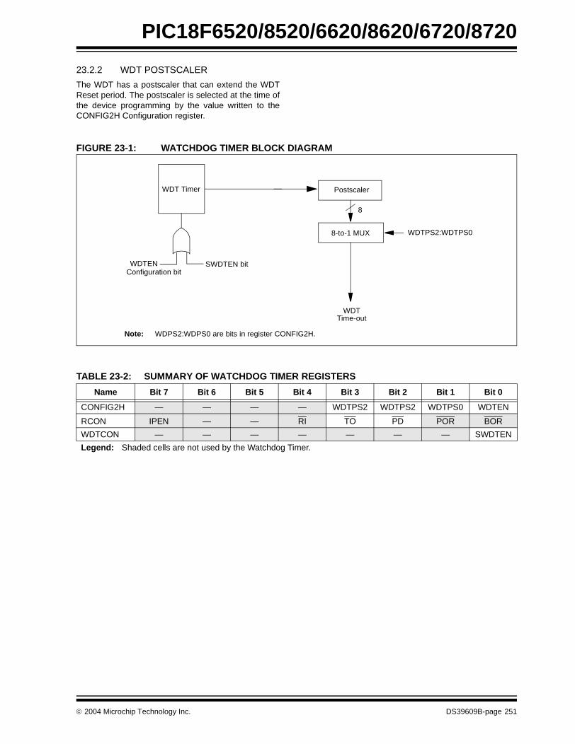
PIC18F6520/8520/6620/8620/6720/8720
23.2.2 WDT POSTSCALER
The WDT has a postscaler that can extend the WDTReset period. The postscaler is selected at the time ofthe device programming by the value written to theCONFIG2H Configuration register.
FIGURE 23-1: WATCHDOG TIMER BLOCK DIAGRAM
TABLE 23-2: SUMMARY OF WATCHDOG TIMER REGISTERS
PostscalerWDT Timer
WDTEN
8-to-1 MUX WDTPS2:WDTPS0
WDTTime-out
8
SWDTEN bit Configuration bit
Note: WDPS2:WDPS0 are bits in register CONFIG2H.
Name Bit 7 Bit 6 Bit 5 Bit 4 Bit 3 Bit 2 Bit 1 Bit 0
CONFIG2H — — — — WDTPS2 WDTPS2 WDTPS0 WDTEN
RCON IPEN — — RI TO PD POR BOR
WDTCON — — — — — — — SWDTEN
Legend: Shaded cells are not used by the Watchdog Timer.
2004 Microchip Technology Inc. DS39609B-page 251
PIC18F6520/8520/6620/8620/6720/8720
23.3 Power-down Mode (Sleep)
Power-down mode is entered by executing a SLEEPinstruction.
If enabled, the Watchdog Timer will be cleared, butkeeps running, the PD bit (RCON<3>) is cleared, theTO (RCON<4>) bit is set and the oscillator driver isturned off. The I/O ports maintain the status they hadbefore the SLEEP instruction was executed (drivinghigh, low or high-impedance).
For lowest current consumption in this mode, place allI/O pins at either VDD or VSS, ensure no external cir-cuitry is drawing current from the I/O pin, power-downthe A/D and disable external clocks. Pull all I/O pinsthat are high-impedance inputs, high or low externally,to avoid switching currents caused by floating inputs.The T0CKI input should also be at VDD or VSS for low-est current consumption. The contribution from on-chippull-ups on PORTB should be considered.
The MCLR pin must be at a logic high level (VIHMC).
23.3.1 WAKE-UP FROM SLEEP
The device can wake-up from Sleep through one of thefollowing events:
1. External Reset input on MCLR pin.2. Watchdog Timer Wake-up (if WDT was
enabled).3. Interrupt from INT pin, RB port change or a
peripheral interrupt.
The following peripheral interrupts can wake the devicefrom Sleep:
1. PSP read or write.2. TMR1 interrupt. Timer1 must be operating as an
asynchronous counter.3. TMR3 interrupt. Timer3 must be operating as an
asynchronous counter.4. CCP Capture mode interrupt.5. Special event trigger (Timer1 in Asynchronous
mode using an external clock).6. MSSP (Start/Stop) bit detect interrupt.
7. MSSP transmit or receive in Slave mode (SPI/I2C).
8. USART RX or TX (Synchronous Slave mode).9. A/D conversion (when A/D clock source is RC).10. EEPROM write operation complete.
11. LVD interrupt.
Other peripherals cannot generate interrupts, sinceduring Sleep, no on-chip clocks are present.
External MCLR Reset will cause a device Reset. Allother events are considered a continuation of programexecution and will cause a “wake-up”. The TO and PDbits in the RCON register can be used to determine thecause of the device Reset. The PD bit, which is set onpower-up, is cleared when Sleep is invoked. The TO bitis cleared if a WDT time-out occurred (and causedwake-up).
When the SLEEP instruction is being executed, the nextinstruction (PC + 2) is prefetched. For the device towake-up through an interrupt event, the correspondinginterrupt enable bit must be set (enabled). Wake-up isregardless of the state of the GIE bit. If the GIE bit isclear (disabled), the device continues execution at theinstruction after the SLEEP instruction. If the GIE bit isset (enabled), the device executes the instruction afterthe SLEEP instruction and then branches to the inter-rupt address. In cases where the execution of theinstruction following SLEEP is not desirable, the usershould have a NOP after the SLEEP instruction.
23.3.2 WAKE-UP USING INTERRUPTS
When global interrupts are disabled (GIE cleared) andany interrupt source has both its interrupt enable bitand interrupt flag bit set, one of the following will occur:
• If an interrupt condition (interrupt flag bit and interrupt enable bits are set) occurs before the execution of a SLEEP instruction, the SLEEP instruction will complete as a NOP. Therefore, the WDT and WDT postscaler will not be cleared, the TO bit will not be set and PD bits will not be cleared.
• If the interrupt condition occurs during or after the execution of a SLEEP instruction, the device will immediately wake-up from Sleep. The SLEEP instruction will be completely executed before the wake-up. Therefore, the WDT and WDT postscaler will be cleared, the TO bit will be set and the PD bit will be cleared.
Even if the flag bits were checked before executing aSLEEP instruction, it may be possible for flag bits tobecome set before the SLEEP instruction completes. Todetermine whether a SLEEP instruction executed, testthe PD bit. If the PD bit is set, the SLEEP instructionwas executed as a NOP.
To ensure that the WDT is cleared, a CLRWDT instructionshould be executed before a SLEEP instruction.
DS39609B-page 252 2004 Microchip Technology Inc.

PIC18F6520/8520/6620/8620/6720/8720
FIGURE 23-2: WAKE-UP FROM SLEEP THROUGH INTERRUPT(1,2)
23.4 Program Verification and Code Protection
The overall structure of the code protection on thePIC18 Flash devices differs significantly from otherPICmicro® devices. The user program memory isdivided on binary boundaries into individual blocks,each of which has three separate code protection bitsassociated with it:
• Code-Protect bit (CPn)• Write-Protect bit (WRTn)• External Block Table Read bit (EBTRn)
The code protection bits are located in ConfigurationRegisters 5L through 7H. Their locations within theregisters are summarized in Table 23-3.
In the PIC18FXX20 family, the block size varies withthe size of the user program memory. For PIC18FX520devices, program memory is divided into four blocks of8 Kbytes each. The first block is further divided into aboot block of 2 Kbytes and a second block (Block 0) of6 Kbytes, for a total of five blocks. The organization ofthe blocks and their associated code protection bits areshown in Figure 23-3.
For PIC18FX620 and PIC18FX720 devices, programmemory is divided into blocks of 16 Kbytes. The firstblock is further divided into a boot block of 512 bytesand a second block (Block 0) of 15.5 Kbytes, for a totalof nine blocks. This produces five blocks for 64-Kbytedevices and nine for 128-Kbyte devices. The organiza-tion of the blocks and their associated code protectionbits are shown in Figure 23-4.
TABLE 23-3: SUMMARY OF CODE PROTECTION REGISTERS
Q1 Q2 Q3 Q4 Q1 Q2 Q3 Q4 Q1 Q1 Q2 Q3 Q4 Q1 Q2 Q3 Q4 Q1 Q2 Q3 Q4 Q1 Q2 Q3 Q4
OSC1
CLKO(4)
INT pin
INTF flag(INTCON<1>)
GIEH bit(INTCON<7>)
INSTRUCTION FLOW
PC
InstructionFetched
InstructionExecuted
PC PC+2 PC+4
Inst(PC) = Sleep
Inst(PC - 1)
Inst(PC + 2)
Sleep
Processor inSleep
Interrupt Latency(3)
Inst(PC + 4)
Inst(PC + 2)
Inst(0008h) Inst(000Ah)
Inst(0008h)Dummy Cycle
PC + 4 0008h 000Ah
Dummy Cycle
TOST(2)
PC+4
Note 1: XT, HS or LP Oscillator mode assumed.2: GIE = 1 assumed. In this case, after wake-up, the processor jumps to the interrupt routine. If GIE = 0, execution will continue in-line.3: TOST = 1024 TOSC (drawing not to scale). This delay will not occur for RC and EC Oscillator modes.4: CLKO is not available in these oscillator modes, but shown here for timing reference.
File Name Bit 7 Bit 6 Bit 5 Bit 4 Bit 3 Bit 2 Bit 1 Bit 0
300008h CONFIG5L CP7(1) CP6(1) CP5(1) CP4(1) CP3 CP2 CP1 CP0
300009h CONFIG5H CPD CPB — — — — — —
30000Ah CONFIG6L WRT7(1) WRT6(1) WRT5(1) WRT4(1) WRT3 WRT2 WRT1 WRT0
30000Bh CONFIG6H WRTD WRTB WRTC — — — — —
30000Ch CONFIG7L EBTR7(1) EBTR6(1) EBTR5(1) EBTR4(1) EBTR3 EBTR2 EBTR1 EBTR0
30000Dh CONFIG7H — EBTRB — — — — — —
Legend: Shaded cells are unimplemented.Note 1: Unimplemented in PIC18FX520 and PIC18FX620 devices.
2004 Microchip Technology Inc. DS39609B-page 253

PIC18F6520/8520/6620/8620/6720/8720
FIGURE 23-3: CODE-PROTECTED PROGRAM MEMORY FOR PIC18FX520 DEVICES
FIGURE 23-4: CODE-PROTECTED PROGRAM MEMORY FOR PIC18FX620/X720 DEVICES
32 Kbytes Address
RangeBlock Code Protection
Controlled By:
Boot Block000000h0007FFh
CPB, WRTB, EBTRB
Block 0000800h001FFFh
CP0, WRT0, EBTR0
Block 1002000h
003FFFhCP1, WRT1, EBTR1
Block 2004000h
005FFFhCP2, WRT2, EBTR2
Block 3006000h
007FFFhCP3, WRT3, EBTR3
UnimplementedRead ‘0’s
008000h
1FFFFFh
MEMORY SIZE/DEVICE Block Code Protection
Controlled By:64 Kbytes(PIC18FX620)
128 Kbytes(PIC18FX720)
Address Range
Boot Block Boot Block000000h0001FFh
CPB, WRTB, EBTRB
Block 0 Block 0000200h003FFFh
CP0, WRT0, EBTR0
Block 1 Block 1004000h
007FFFhCP1, WRT1, EBTR1
Block 2 Block 2008000h
00BFFFhCP2, WRT2, EBTR2
Block 3 Block 300C000h
00FFFFhCP3, WRT3, EBTR3
UnimplementedRead ‘0’s
Block 4010000h
013FFFhCP4, WRT4, EBTR4
Block 5014000h
017FFFhCP5, WRT5, EBTR5
Block 6018000h
01BFFFhCP6, WRT6, EBTR6
Block 701C000h
01FFFFhCP7, WRT7, EBTR7
DS39609B-page 254 2004 Microchip Technology Inc.
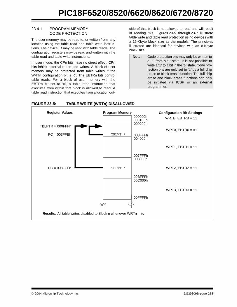
PIC18F6520/8520/6620/8620/6720/8720
23.4.1 PROGRAM MEMORYCODE PROTECTION
The user memory may be read to, or written from, anylocation using the table read and table write instruc-tions. The device ID may be read with table reads. Theconfiguration registers may be read and written with thetable read and table write instructions.
In user mode, the CPn bits have no direct effect. CPnbits inhibit external reads and writes. A block of usermemory may be protected from table writes if theWRTn configuration bit is ‘0’. The EBTRn bits controltable reads. For a block of user memory with theEBTRn bit set to ‘0’, a table read instruction thatexecutes from within that block is allowed to read. Atable read instruction that executes from a location out-
side of that block is not allowed to read and will resultin reading ‘0’s. Figures 23-5 through 23-7 illustratetable write and table read protection using devices witha 16-Kbyte block size as the models. The principlesillustrated are identical for devices with an 8-Kbyteblock size.
FIGURE 23-5: TABLE WRITE (WRTn) DISALLOWED
Note: Code protection bits may only be written toa ‘0’ from a ‘1’ state. It is not possible towrite a ‘1’ to a bit in the ‘0’ state. Code pro-tection bits are only set to ‘1’ by a full chiperase or block erase function. The full chiperase and block erase functions can onlybe initiated via ICSP or an externalprogrammer.
000000h0001FFh000200h
003FFFh004000h
007FFFh008000h
00BFFFh00C000h
00FFFFh
WRTB, EBTRB = 11
WRT0, EBTR0 = 01
WRT1, EBTR1 = 11
WRT2, EBTR2 = 11
WRT3, EBTR3 = 11
TBLWT *
TBLPTR = 000FFFh
PC = 003FFEh
TBLWT *PC = 008FFEh
Register Values Program Memory Configuration Bit Settings
Results: All table writes disabled to Block n whenever WRTn = 0.
2004 Microchip Technology Inc. DS39609B-page 255

PIC18F6520/8520/6620/8620/6720/8720
FIGURE 23-6: EXTERNAL BLOCK TABLE READ (EBTRn) DISALLOWED
FIGURE 23-7: EXTERNAL BLOCK TABLE READ (EBTRn) ALLOWED
WRTB, EBTRB = 11
WRT0, EBTR0 = 10
WRT1, EBTR1 = 11
WRT2, EBTR2 = 11
WRT3, EBTR3 = 11
TBLRD *
TBLPTR = 000FFFh
PC = 004FFEh
Results: All table reads from external blocks to Block n are disabled whenever EBTRn = 0.TABLAT register returns a value of ‘0’.
Register Values Program Memory Configuration Bit Settings
0001FFh000200h
003FFFh004000h
007FFFh008000h
00BFFFh00C000h
00FFFFh
000000h
WRTB, EBTRB = 11
WRT0, EBTR0 = 10
WRT1, EBTR1 = 11
WRT2, EBTR2 = 11
WRT3, EBTR3 = 11
TBLRD *
TBLPTR = 000FFFh
PC = 003FFEh
Register Values Program Memory Configuration Bit Settings
Results: Table reads permitted within Block n, even when EBTRBn = 0.TABLAT register returns the value of the data at the location TBLPTR.
0001FFh000200h
003FFFh004000h
007FFFh008000h
00BFFFh00C000h
00FFFFh
000000h
DS39609B-page 256 2004 Microchip Technology Inc.

PIC18F6520/8520/6620/8620/6720/8720
23.4.2 DATA EEPROM CODE PROTECTION
The entire data EEPROM is protected from externalreads and writes by two bits: CPD and WRTD. CPDinhibits external reads and writes of data EEPROM.WRTD inhibits external writes to data EEPROM. TheCPU can continue to read and write data EEPROM,regardless of the protection bit settings.
23.4.3 CONFIGURATION REGISTER PROTECTION
The configuration registers can be write-protected. TheWRTC bit controls protection of the configuration regis-ters. In user mode, the WRTC bit is readable only.WRTC can only be written via ICSP or an externalprogrammer.
23.5 ID Locations
Eight memory locations (200000h-200007h) aredesignated as ID locations, where the user can storechecksum or other code identification numbers. Theselocations are accessible during normal executionthrough the TBLRD and TBLWT instructions or duringprogram/verify. The ID locations can be read when thedevice is code-protected.
23.6 In-Circuit Serial Programming
PIC18FX520/X620/X720 microcontrollers can be seri-ally programmed while in the end application circuit.This is simply done with two lines for clock and dataand three other lines for power, ground and theprogramming voltage. This allows customers to manu-facture boards with unprogrammed devices and thenprogram the microcontroller just before shipping theproduct. This also allows the most recent firmware or acustom firmware to be programmed.
23.7 In-Circuit Debugger
When the DEBUG bit in the CONFIG4L Configurationregister is programmed to a ‘0’, the In-Circuit Debuggerfunctionality is enabled. This function allows simpledebugging functions when used with MPLAB® IDE.When the microcontroller has this feature enabled,some of the resources are not available for generaluse. Table 23-4 shows which features are consumedby the background debugger.
TABLE 23-4: DEBUGGER RESOURCES
To use the In-Circuit Debugger function of the micro-controller, the design must implement In-Circuit SerialProgramming connections to MCLR/VPP, VDD, GND,RB7 and RB6. This will interface to the In-CircuitDebugger module available from Microchip or one ofthe third party development tool companies.
23.8 Low-Voltage ICSP Programming
The LVP bit in the CONFIG4L Configuration registerenables Low-Voltage ICSP Programming. This modeallows the microcontroller to be programmed via ICSPusing a VDD source in the operating voltage range. Thisonly means that VPP does not have to be brought toVIHH, but can instead be left at the normal operatingvoltage. In this mode, the RB5/PGM pin is dedicated tothe programming function and ceases to be a generalpurpose I/O pin. During programming, VDD is applied tothe MCLR/VPP pin. To enter Programming mode, VDD
must be applied to the RB5/PGM pin, provided the LVPbit is set. The LVP bit defaults to a ‘1’ from the factory.
If Low-Voltage Programming mode is not used, the LVPbit can be programmed to a ‘0’ and RB5/PGM becomesa digital I/O pin. However, the LVP bit may only beprogrammed when programming is entered with VIHH
on MCLR/VPP.
It should be noted that once the LVP bit is programmedto ‘0’, only the High-Voltage Programming mode isavailable and only High-Voltage Programming modecan be used to program the device.
When using Low-Voltage ICSP Programming, the partmust be supplied 4.5V to 5.5V if a bulk erase will beexecuted. This includes reprogramming of the code-protect bits from an on state to an off state. For all othercases of Low-Voltage ICSP, the part may beprogrammed at the normal operating voltage. Thismeans unique user IDs or user code can bereprogrammed or added.
Note: When performing In-Circuit SerialProgramming, verify that power is con-nected to all VDD and AVDD pins of themicrocontroller and that all VSS and AVSS
pins are grounded.
I/O pins RB6, RB7Stack 2 levelsProgram Memory Last 576 bytesData Memory Last 10 bytes
Note 1: The High-Voltage Programming mode isalways available, regardless of the stateof the LVP bit, by applying VIHH to theMCLR pin.
2: While in Low-Voltage ICSP mode, theRB5 pin can no longer be used as ageneral purpose I/O pin and should beheld low during normal operation.
3: When using Low-Voltage ICSP Program-ming (LVP) and the pull-ups on PORTB areenabled, bit 5 in the TRISB register must becleared to disable the pull-up on RB5 andensure the proper operation of the device.
2004 Microchip Technology Inc. DS39609B-page 257

PIC18F6520/8520/6620/8620/6720/8720
NOTES:
DS39609B-page 258 2004 Microchip Technology Inc.
PIC18F6520/8520/6620/8620/6720/8720
24.0 INSTRUCTION SET SUMMARY
The PIC18 instruction set adds many enhancements tothe previous PICmicro instruction sets, while maintain-ing an easy migration from these PICmicro instructionsets.
Most instructions are a single program memory word(16 bits), but there are three instructions that requiretwo program memory locations.
Each single-word instruction is a 16-bit word dividedinto an opcode, which specifies the instruction type andone or more operands, which further specify theoperation of the instruction.
The instruction set is highly orthogonal and is groupedinto four basic categories:
• Byte-oriented operations• Bit-oriented operations• Literal operations
• Control operations
The PIC18 instruction set summary in Table 24-1 listsbyte-oriented, bit-oriented, literal and controloperations. Table 24-1 shows the opcode fielddescriptions.
Most byte-oriented instructions have three operands:
1. The file register (specified by ‘f’) 2. The destination of the result
(specified by ‘d’) 3. The accessed memory
(specified by ‘a’)
The file register designator ‘f’ specifies which fileregister is to be used by the instruction.
The destination designator ‘d’ specifies where theresult of the operation is to be placed. If ‘d’ is zero, theresult is placed in the WREG register. If ‘d’ is one, theresult is placed in the file register specified in theinstruction.
All bit-oriented instructions have three operands:
1. The file register (specified by ‘f’) 2. The bit in the file register
(specified by ‘b’) 3. The accessed memory
(specified by ‘a’)
The bit field designator ‘b’ selects the number of the bitaffected by the operation, while the file register desig-nator ‘f’ represents the number of the file in which thebit is located.
The literal instructions may use some of the followingoperands:
• A literal value to be loaded into a file register (specified by ‘k’)
• The desired FSR register to load the literal value into (specified by ‘f’)
• No operand required (specified by ‘—’)
The control instructions may use some of the followingoperands:
• A program memory address (specified by ‘n’)• The mode of the CALL or RETURN instructions
(specified by ‘s’)• The mode of the table read and table write
instructions (specified by ‘m’)• No operand required
(specified by ‘—’)
All instructions are a single word, except for threedouble-word instructions. These three instructionswere made double-word instructions so that all therequired information is available in these 32 bits. In thesecond word, the 4 MSbs are ‘1’s. If this second wordis executed as an instruction (by itself), it will executeas a NOP.
All single-word instructions are executed in a singleinstruction cycle, unless a conditional test is true or theprogram counter is changed as a result of the instruc-tion. In these cases, the execution takes two instructioncycles, with the additional instruction cycle(s) executedas a NOP.
The double-word instructions execute in two instructioncycles.
One instruction cycle consists of four oscillator periods.Thus, for an oscillator frequency of 4 MHz, the normalinstruction execution time is 1 µs. If a conditional test istrue, or the program counter is changed as a result ofan instruction, the instruction execution time is 2 µs.Two-word branch instructions (if true) would take 3 µs.
Figure 24-1 shows the general formats that theinstructions can have.
All examples use the format ‘nnh’ to represent a hexa-decimal number, where ‘h’ signifies a hexadecimaldigit.
The Instruction Set Summary, shown in Table 24-1,lists the instructions recognized by the MicrochipAssembler (MPASMTM).
Section 24.1 “Instruction Set” provides a descriptionof each instruction.
2004 Microchip Technology Inc. DS39609B-page 259

PIC18F6520/8520/6620/8620/6720/8720
TABLE 24-1: OPCODE FIELD DESCRIPTIONS
Field Description
a RAM access bita = 0: RAM location in Access RAM (BSR register is ignored)a = 1: RAM bank is specified by BSR register
bbb Bit address within an 8-bit file register (0 to 7).
BSR Bank Select Register. Used to select the current RAM bank.
d Destination select bitd = 0: store result in WREGd = 1: store result in file register f
dest Destination either the WREG register or the specified register file location.
f 8-bit Register file address (0x00 to 0xFF).
fs 12-bit Register file address (0x000 to 0xFFF). This is the source address.
fd 12-bit Register file address (0x000 to 0xFFF). This is the destination address.
k Literal field, constant data or label (may be either an 8-bit, 12-bit or a 20-bit value).
label Label name.
mm The mode of the TBLPTR register for the table read and table write instructions.Only used with table read and table write instructions:
* No Change to register (such as TBLPTR with table reads and writes)*+ Post-Increment register (such as TBLPTR with table reads and writes)*- Post-Decrement register (such as TBLPTR with table reads and writes)+* Pre-Increment register (such as TBLPTR with table reads and writes)
n The relative address (2’s complement number) for relative branch instructions, or the direct address for Call/Branch and Return instructions.
PRODH Product of Multiply High Byte.
PRODL Product of Multiply Low Byte.
s Fast Call/Return mode select bits = 0: do not update into/from shadow registerss = 1: certain registers loaded into/from shadow registers (Fast mode)
u Unused or Unchanged.
WREG Working register (accumulator).
x Don’t care (‘0’ or ‘1’).The assembler will generate code with x = 0. It is the recommended form of use for compatibility with all Microchip software tools.
TBLPTR 21-bit Table Pointer (points to a Program Memory location).
TABLAT 8-bit Table Latch.
TOS Top-of-Stack.
PC Program Counter.
PCL Program Counter Low Byte.
PCH Program Counter High Byte.
PCLATH Program Counter High Byte Latch.
PCLATU Program Counter Upper Byte Latch.
GIE Global Interrupt Enable bit.
WDT Watchdog Timer.
TO Time-out bit.
PD Power-down bit.
C, DC, Z, OV, N ALU Status bits: Carry, Digit Carry, Zero, Overflow, Negative.
[ ] Optional.
( ) Contents.
→ Assigned to.
< > Register bit field.
∈ In the set of.
italics User defined term (font is courier).
DS39609B-page 260 2004 Microchip Technology Inc.
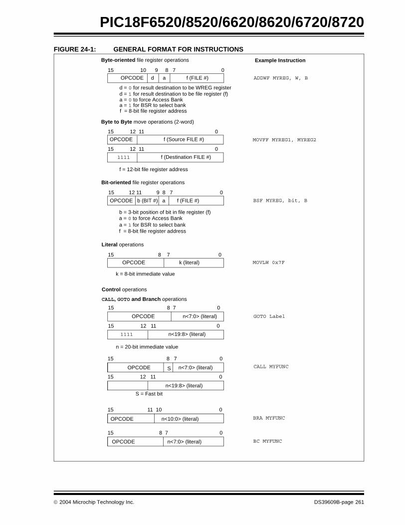
PIC18F6520/8520/6620/8620/6720/8720
FIGURE 24-1: GENERAL FORMAT FOR INSTRUCTIONS
Byte-oriented file register operations
15 10 9 8 7 0
d = 0 for result destination to be WREG register
OPCODE d a f (FILE #)
d = 1 for result destination to be file register (f)a = 0 to force Access Bank
Bit-oriented file register operations
15 12 11 9 8 7 0
OPCODE b (BIT #) a f (FILE #)
b = 3-bit position of bit in file register (f)
Literal operations
15 8 7 0
OPCODE k (literal)
k = 8-bit immediate value
Byte to Byte move operations (2-word)
15 12 11 0
OPCODE f (Source FILE #)
CALL, GOTO and Branch operations
15 8 7 0
OPCODE n<7:0> (literal)
n = 20-bit immediate value
a = 1 for BSR to select bankf = 8-bit file register address
a = 0 to force Access Banka = 1 for BSR to select bankf = 8-bit file register address
15 12 11 0
1111 n<19:8> (literal)
15 12 11 0
1111 f (Destination FILE #)
f = 12-bit file register address
Control operations
Example Instruction
ADDWF MYREG, W, B
MOVFF MYREG1, MYREG2
BSF MYREG, bit, B
MOVLW 0x7F
GOTO Label
15 8 7 0
OPCODE n<7:0> (literal)
15 12 11 0
n<19:8> (literal)
CALL MYFUNC
15 11 10 0
OPCODE n<10:0> (literal)
S = Fast bit
BRA MYFUNC
15 8 7 0
OPCODE n<7:0> (literal) BC MYFUNC
S
2004 Microchip Technology Inc. DS39609B-page 261

PIC18F6520/8520/6620/8620/6720/8720
TABLE 24-1: PIC18FXXXX INSTRUCTION SET
Mnemonic,Operands
Description Cycles16-Bit Instruction Word Status
AffectedNotes
MSb LSb
BYTE-ORIENTED FILE REGISTER OPERATIONS
ADDWFADDWFCANDWFCLRFCOMFCPFSEQCPFSGTCPFSLTDECFDECFSZDCFSNZINCFINCFSZINFSNZIORWFMOVFMOVFF
MOVWFMULWFNEGFRLCFRLNCFRRCFRRNCFSETFSUBFWB
SUBWFSUBWFB
SWAPFTSTFSZXORWF
f, d, af, d, af, d, af, af, d, af, af, af, af, d, af, d, af, d, af, d, af, d, af, d, af, d, af, d, afs, fd
f, af, af, af, d, af, d, af, d, af, d, af, af, d, a
f, d, af, d, a
f, d, af, af, d, a
Add WREG and fAdd WREG and Carry bit to fAND WREG with fClear fComplement fCompare f with WREG, skip =Compare f with WREG, skip >Compare f with WREG, skip <Decrement fDecrement f, Skip if 0Decrement f, Skip if Not 0Increment fIncrement f, Skip if 0Increment f, Skip if Not 0Inclusive OR WREG with fMove fMove fs (source) to 1st word
fd (destination) 2nd wordMove WREG to fMultiply WREG with fNegate fRotate Left f through CarryRotate Left f (No Carry)Rotate Right f through CarryRotate Right f (No Carry)Set fSubtract f from WREG with borrow Subtract WREG from fSubtract WREG from f with borrowSwap nibbles in fTest f, skip if 0Exclusive OR WREG with f
111111 (2 or 3)1 (2 or 3)1 (2 or 3)11 (2 or 3)1 (2 or 3)11 (2 or 3)1 (2 or 3)112
111111111
11
11 (2 or 3)1
001000100001011000010110011001100000001001000010001101000001010111001111011000000110001101000011010001100101
01010101
001101100001
01da00da01da101a11da001a010a000a01da11da11da10da11da10da00da00daffffffff111a001a110a01da01da00da00da100a01da
11da10da
10da011a10da
ffffffffffffffffffffffffffffffffffffffffffffffffffffffffffffffffffffffffffffffffffffffffffffffffffffffffffff
ffffffff
ffffffffffff
ffffffffffffffffffffffffffffffffffffffffffffffffffffffffffffffffffffffffffffffffffffffffffffffffffffffffffff
ffffffff
ffffffffffff
C, DC, Z, OV, NC, DC, Z, OV, NZ, NZZ, NNoneNoneNoneC, DC, Z, OV, NNoneNoneC, DC, Z, OV, NNoneNoneZ, NZ, NNone
NoneNoneC, DC, Z, OV, NC, Z, NZ, NC, Z, NZ, NNoneC, DC, Z, OV, N
C, DC, Z, OV, NC, DC, Z, OV, N
NoneNoneZ, N
1, 21, 21,221, 2441, 21, 2, 3, 41, 2, 3, 41, 21, 2, 3, 441, 21, 21
1, 2
1, 2
1, 2
1, 2
41, 2
BIT-ORIENTED FILE REGISTER OPERATIONS
BCFBSFBTFSCBTFSSBTG
f, b, af, b, af, b, af, b, af, d, a
Bit Clear fBit Set fBit Test f, Skip if ClearBit Test f, Skip if SetBit Toggle f
111 (2 or 3)1 (2 or 3)1
10011000101110100111
bbbabbbabbbabbbabbba
ffffffffffffffffffff
ffffffffffffffffffff
NoneNoneNoneNoneNone
1, 21, 23, 43, 41, 2
Note 1: When a Port register is modified as a function of itself (e.g., MOVF PORTB, 1, 0), the value used will be that value present on the pins themselves. For example, if the data latch is ‘1’ for a pin configured as input and is driven low by an external device, the data will be written back with a ‘0’.
2: If this instruction is executed on the TMR0 register (and where applicable, d = 1), the prescaler will be cleared if assigned.
3: If Program Counter (PC) is modified or a conditional test is true, the instruction requires two cycles. The second cycle is executed as a NOP.
4: Some instructions are 2-word instructions. The second word of these instructions will be executed as a NOP unless the first word of the instruction retrieves the information embedded in these 16 bits. This ensures that all program memory locations have a valid instruction.
5: If the table write starts the write cycle to internal memory, the write will continue until terminated.
DS39609B-page 262 2004 Microchip Technology Inc.
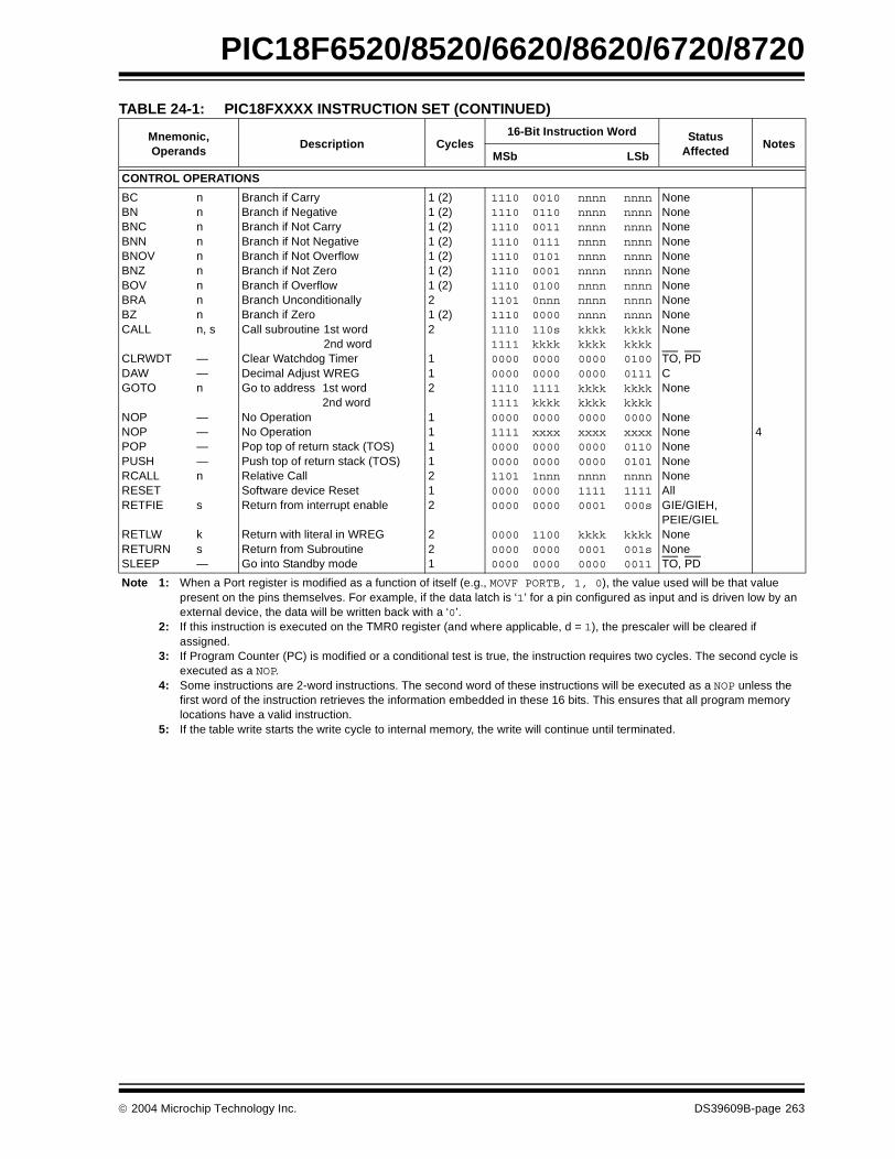
PIC18F6520/8520/6620/8620/6720/8720
CONTROL OPERATIONS
BCBNBNCBNNBNOVBNZBOVBRABZCALL
CLRWDTDAWGOTO
NOPNOPPOPPUSHRCALLRESETRETFIE
RETLWRETURNSLEEP
nnnnnnnnnn, s
——n
————n
s
ks—
Branch if CarryBranch if NegativeBranch if Not CarryBranch if Not NegativeBranch if Not OverflowBranch if Not ZeroBranch if OverflowBranch Unconditionally Branch if ZeroCall subroutine 1st word
2nd wordClear Watchdog TimerDecimal Adjust WREGGo to address 1st word
2nd wordNo OperationNo OperationPop top of return stack (TOS)Push top of return stack (TOS)Relative CallSoftware device ResetReturn from interrupt enable
Return with literal in WREG Return from SubroutineGo into Standby mode
1 (2)1 (2)1 (2)1 (2)1 (2)1 (2)1 (2)21 (2)2
112
1111212
221
1110111011101110111011101110110111101110111100000000111011110000111100000000110100000000
000000000000
00100110001101110101000101000nnn0000110skkkk000000001111kkkk0000xxxx000000001nnn00000000
110000000000
nnnnnnnnnnnnnnnnnnnnnnnnnnnnnnnnnnnnkkkkkkkk00000000kkkkkkkk0000xxxx00000000nnnn11110001
kkkk00010000
nnnnnnnnnnnnnnnnnnnnnnnnnnnnnnnnnnnnkkkkkkkk01000111kkkkkkkk0000xxxx01100101nnnn1111000s
kkkk001s0011
NoneNoneNoneNoneNoneNoneNoneNoneNoneNone
TO, PDCNone
NoneNoneNoneNoneNoneAllGIE/GIEH, PEIE/GIELNoneNoneTO, PD
4
TABLE 24-1: PIC18FXXXX INSTRUCTION SET (CONTINUED)
Mnemonic,Operands
Description Cycles16-Bit Instruction Word Status
AffectedNotes
MSb LSb
Note 1: When a Port register is modified as a function of itself (e.g., MOVF PORTB, 1, 0), the value used will be that value present on the pins themselves. For example, if the data latch is ‘1’ for a pin configured as input and is driven low by an external device, the data will be written back with a ‘0’.
2: If this instruction is executed on the TMR0 register (and where applicable, d = 1), the prescaler will be cleared if assigned.
3: If Program Counter (PC) is modified or a conditional test is true, the instruction requires two cycles. The second cycle is executed as a NOP.
4: Some instructions are 2-word instructions. The second word of these instructions will be executed as a NOP unless the first word of the instruction retrieves the information embedded in these 16 bits. This ensures that all program memory locations have a valid instruction.
5: If the table write starts the write cycle to internal memory, the write will continue until terminated.
2004 Microchip Technology Inc. DS39609B-page 263
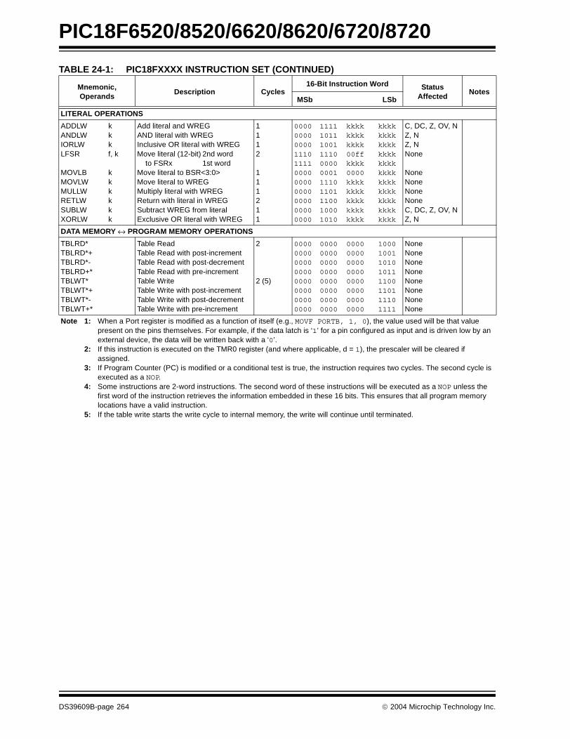
PIC18F6520/8520/6620/8620/6720/8720
LITERAL OPERATIONS
ADDLWANDLWIORLWLFSR
MOVLBMOVLWMULLWRETLWSUBLWXORLW
kkkf, k
kkkkkk
Add literal and WREGAND literal with WREGInclusive OR literal with WREGMove literal (12-bit) 2nd word to FSRx 1st wordMove literal to BSR<3:0>Move literal to WREGMultiply literal with WREGReturn with literal in WREG Subtract WREG from literalExclusive OR literal with WREG
1112
111211
00000000000011101111000000000000000000000000
11111011100111100000000111101101110010001010
kkkkkkkkkkkk00ffkkkk0000kkkkkkkkkkkkkkkkkkkk
kkkkkkkkkkkkkkkkkkkkkkkkkkkkkkkkkkkkkkkkkkkk
C, DC, Z, OV, NZ, NZ, NNone
NoneNoneNoneNoneC, DC, Z, OV, NZ, N
DATA MEMORY ↔ PROGRAM MEMORY OPERATIONS
TBLRD*TBLRD*+TBLRD*-TBLRD+*TBLWT*TBLWT*+TBLWT*-TBLWT+*
Table ReadTable Read with post-incrementTable Read with post-decrementTable Read with pre-incrementTable WriteTable Write with post-incrementTable Write with post-decrementTable Write with pre-increment
2
2 (5)
00000000000000000000000000000000
00000000000000000000000000000000
00000000000000000000000000000000
10001001101010111100110111101111
NoneNoneNoneNoneNoneNoneNoneNone
TABLE 24-1: PIC18FXXXX INSTRUCTION SET (CONTINUED)
Mnemonic,Operands
Description Cycles16-Bit Instruction Word Status
AffectedNotes
MSb LSb
Note 1: When a Port register is modified as a function of itself (e.g., MOVF PORTB, 1, 0), the value used will be that value present on the pins themselves. For example, if the data latch is ‘1’ for a pin configured as input and is driven low by an external device, the data will be written back with a ‘0’.
2: If this instruction is executed on the TMR0 register (and where applicable, d = 1), the prescaler will be cleared if assigned.
3: If Program Counter (PC) is modified or a conditional test is true, the instruction requires two cycles. The second cycle is executed as a NOP.
4: Some instructions are 2-word instructions. The second word of these instructions will be executed as a NOP unless the first word of the instruction retrieves the information embedded in these 16 bits. This ensures that all program memory locations have a valid instruction.
5: If the table write starts the write cycle to internal memory, the write will continue until terminated.
DS39609B-page 264 2004 Microchip Technology Inc.

PIC18F6520/8520/6620/8620/6720/8720
24.1 Instruction Set
ADDLW ADD literal to W
Syntax: [ label ] ADDLW k
Operands: 0 ≤ k ≤ 255
Operation: (W) + k → W
Status Affected: N, OV, C, DC, Z
Encoding: 0000 1111 kkkk kkkk
Description: The contents of W are added to the 8-bit literal ‘k’ and the result is placed in W.
Words: 1
Cycles: 1
Q Cycle Activity:Q1 Q2 Q3 Q4
Decode Readliteral ‘k’
Process Data
Write to W
Example: ADDLW 0x15
Before InstructionW = 0x10
After InstructionW = 0x25
ADDWF ADD W to f
Syntax: [ label ] ADDWF f [,d [,a] f [,d [,a]
Operands: 0 ≤ f ≤ 255d ∈ [0,1]a ∈ [0,1]
Operation: (W) + (f) → dest
Status Affected: N, OV, C, DC, Z
Encoding: 0010 01da ffff ffff
Description: Add W to register ‘f’. If ‘d’ is ‘0’, the result is stored in W. If ‘d’ is ‘1’, the result is stored back in register ‘f’ (default). If ‘a’ is ‘0’, the Access Bank will be selected. If ‘a’ is ‘1’, the BSR is used.
Words: 1
Cycles: 1
Q Cycle Activity:
Q1 Q2 Q3 Q4Decode Read
register ‘f’Process
DataWrite to
destination
Example: ADDWF REG, 0, 0
Before InstructionW = 0x17REG = 0xC2
After InstructionW = 0xD9REG = 0xC2
2004 Microchip Technology Inc. DS39609B-page 265

PIC18F6520/8520/6620/8620/6720/8720
ADDWFC ADD W and Carry bit to f
Syntax: [ label ] ADDWFC f [,d [,a]
Operands: 0 ≤ f ≤ 255d ∈ [0,1]a ∈ [0,1]
Operation: (W) + (f) + (C) → dest
Status Affected: N, OV, C, DC, Z
Encoding: 0010 00da ffff ffff
Description: Add W, the Carry flag and data memory location ‘f’. If ‘d’ is ‘0’, the result is placed in W. If ‘d’ is ‘1’, the result is placed in data memory location ‘f’. If ‘a’ is ‘0’, the Access Bank will be selected. If ‘a’ is ‘1’, the BSR will not be overridden.
Words: 1
Cycles: 1
Q Cycle Activity:
Q1 Q2 Q3 Q4Decode Read
register ‘f’Process
DataWrite to
destination
Example: ADDWFC REG, 0, 1
Before InstructionCarry bit = 1REG = 0x02W = 0x4D
After InstructionCarry bit = 0REG = 0x02W = 0x50
ANDLW AND literal with W
Syntax: [ label ] ANDLW k
Operands: 0 ≤ k ≤ 255
Operation: (W) .AND. k → W
Status Affected: N, Z
Encoding: 0000 1011 kkkk kkkk
Description: The contents of W are AND’ed with the 8-bit literal ‘k’. The result is placed in W.
Words: 1
Cycles: 1
Q Cycle Activity:
Q1 Q2 Q3 Q4Decode Read literal
‘k’Process
DataWrite to W
Example: ANDLW 0x5F
Before InstructionW = 0xA3
After InstructionW = 0x03
DS39609B-page 266 2004 Microchip Technology Inc.

PIC18F6520/8520/6620/8620/6720/8720
ANDWF AND W with f
Syntax: [ label ] ANDWF f [,d [,a]
Operands: 0 ≤ f ≤ 255d ∈ [0,1]a ∈ [0,1]
Operation: (W) .AND. (f) → dest
Status Affected: N, Z
Encoding: 0001 01da ffff ffff
Description: The contents of W are AND’ed with register ‘f’. If ‘d’ is ‘0’, the result is stored in W. If ‘d’ is ‘1’, the result is stored back in register ‘f’ (default). If ‘a’ is ‘0’, the Access Bank will be selected. If ‘a’ is ‘1’, the BSR will not be overridden (default).
Words: 1
Cycles: 1
Q Cycle Activity:
Q1 Q2 Q3 Q4Decode Read
register ‘f’Process
DataWrite to
destination
Example: ANDWF REG, 0, 0
Before InstructionW = 0x17REG = 0xC2
After Instruction
W = 0x02REG = 0xC2
BC Branch if Carry
Syntax: [ label ] BC n
Operands: -128 ≤ n ≤ 127
Operation: if Carry bit is ‘1’ (PC) + 2 + 2n → PC
Status Affected: None
Encoding: 1110 0010 nnnn nnnn
Description: If the Carry bit is ‘1’, then the program will branch.The 2’s complement number ‘2n’ is added to the PC. Since the PC will have incremented to fetch the next instruction, the new address will be PC+2+2n. This instruction is then a two-cycle instruction.
Words: 1
Cycles: 1(2)
Q Cycle Activity:If Jump:
Q1 Q2 Q3 Q4Decode Read literal
‘n’Process
DataWrite to PC
No operation
No operation
No operation
No operation
If No Jump:
Q1 Q2 Q3 Q4Decode Read literal
‘n’Process
DataNo
operation
Example: HERE BC 5
Before InstructionPC = address (HERE)
After InstructionIf Carry = 1;
PC = address (HERE+12)If Carry = 0;
PC = address (HERE+2)
2004 Microchip Technology Inc. DS39609B-page 267

PIC18F6520/8520/6620/8620/6720/8720
BCF Bit Clear f
Syntax: [ label ] BCF f,b[,a]
Operands: 0 ≤ f ≤ 2550 ≤ b ≤ 7a ∈ [0,1]
Operation: 0 → f<b>
Status Affected: None
Encoding: 1001 bbba ffff ffff
Description: Bit ‘b’ in register ‘f’ is cleared. If ‘a’ is ‘0’, the Access Bank will be selected, overriding the BSR value. If ‘a’ = 1, then the bank will be selected as per the BSR value (default).
Words: 1
Cycles: 1
Q Cycle Activity:Q1 Q2 Q3 Q4
Decode Readregister ‘f’
Process Data
Writeregister ‘f’
Example: BCF FLAG_REG, 7, 0
Before InstructionFLAG_REG = 0xC7
After InstructionFLAG_REG = 0x47
BN Branch if Negative
Syntax: [ label ] BN n
Operands: -128 ≤ n ≤ 127
Operation: if Negative bit is ‘1’(PC) + 2 + 2n → PC
Status Affected: None
Encoding: 1110 0110 nnnn nnnn
Description: If the Negative bit is ‘1’, then the program will branch.The 2’s complement number ‘2n’ is added to the PC. Since the PC will have incremented to fetch the next instruction, the new address will be PC+2+2n. This instruction is then a two-cycle instruction.
Words: 1
Cycles: 1(2)
Q Cycle Activity:If Jump:
Q1 Q2 Q3 Q4Decode Read literal
‘n’Process
DataWrite to PC
No operation
No operation
No operation
No operation
If No Jump:
Q1 Q2 Q3 Q4Decode Read literal
‘n’Process
DataNo
operation
Example: HERE BN Jump
Before InstructionPC = address (HERE)
After InstructionIf Negative = 1;
PC = address (Jump)If Negative = 0;
PC = address (HERE+2)
DS39609B-page 268 2004 Microchip Technology Inc.

PIC18F6520/8520/6620/8620/6720/8720
BNC Branch if Not Carry
Syntax: [ label ] BNC n
Operands: -128 ≤ n ≤ 127
Operation: if Carry bit is ‘0’(PC) + 2 + 2n → PC
Status Affected: None
Encoding: 1110 0011 nnnn nnnn
Description: If the Carry bit is ‘0’, then the program will branch.The 2’s complement number ‘2n’ is added to the PC. Since the PC will have incremented to fetch the next instruction, the new address will be PC+2+2n. This instruction is then a two-cycle instruction.
Words: 1
Cycles: 1(2)
Q Cycle Activity:If Jump:
Q1 Q2 Q3 Q4Decode Read literal
‘n’Process
DataWrite to PC
No operation
No operation
No operation
No operation
If No Jump:
Q1 Q2 Q3 Q4Decode Read literal
‘n’Process
DataNo
operation
Example: HERE BNC Jump
Before InstructionPC = address (HERE)
After InstructionIf Carry = 0;
PC = address (Jump)If Carry = 1;
PC = address (HERE+2)
BNN Branch if Not Negative
Syntax: [ label ] BNN n
Operands: -128 ≤ n ≤ 127
Operation: if Negative bit is ‘0’(PC) + 2 + 2n → PC
Status Affected: None
Encoding: 1110 0111 nnnn nnnn
Description: If the Negative bit is ‘0’, then the program will branch.The 2’s complement number ‘2n’ is added to the PC. Since the PC will have incremented to fetch the next instruction, the new address will be PC+2+2n. This instruction is then a two-cycle instruction.
Words: 1
Cycles: 1(2)
Q Cycle Activity:If Jump:
Q1 Q2 Q3 Q4Decode Read literal
‘n’Process
DataWrite to PC
No operation
No operation
No operation
No operation
If No Jump:
Q1 Q2 Q3 Q4Decode Read literal
‘n’Process
DataNo
operation
Example: HERE BNN Jump
Before InstructionPC = address (HERE)
After InstructionIf Negative = 0;
PC = address (Jump)If Negative = 1;
PC = address (HERE+2)
2004 Microchip Technology Inc. DS39609B-page 269

PIC18F6520/8520/6620/8620/6720/8720
BNOV Branch if Not Overflow
Syntax: [ label ] BNOV n
Operands: -128 ≤ n ≤ 127
Operation: if Overflow bit is ‘0’(PC) + 2 + 2n → PC
Status Affected: None
Encoding: 1110 0101 nnnn nnnn
Description: If the Overflow bit is ‘0’, then the program will branch.The 2’s complement number ‘2n’ is added to the PC. Since the PC will have incremented to fetch the next instruction, the new address will be PC+2+2n. This instruction is then a two-cycle instruction.
Words: 1
Cycles: 1(2)
Q Cycle Activity:If Jump:
Q1 Q2 Q3 Q4Decode Read literal
‘n’Process
DataWrite to PC
No operation
No operation
No operation
No operation
If No Jump:
Q1 Q2 Q3 Q4Decode Read literal
‘n’Process
DataNo
operation
Example: HERE BNOV Jump
Before InstructionPC = address (HERE)
After InstructionIf Overflow = 0;
PC = address (Jump)If Overflow = 1;
PC = address (HERE+2)
BNZ Branch if Not Zero
Syntax: [ label ] BNZ n
Operands: -128 ≤ n ≤ 127
Operation: if Zero bit is ‘0’(PC) + 2 + 2n → PC
Status Affected: None
Encoding: 1110 0001 nnnn nnnn
Description: If the Zero bit is ‘0’, then the program will branch.The 2’s complement number ‘2n’ is added to the PC. Since the PC will have incremented to fetch the next instruction, the new address will be PC+2+2n. This instruction is then a two-cycle instruction.
Words: 1
Cycles: 1(2)
Q Cycle Activity:If Jump:
Q1 Q2 Q3 Q4Decode Read literal
‘n’Process
DataWrite to PC
No operation
No operation
No operation
No operation
If No Jump:
Q1 Q2 Q3 Q4Decode Read literal
‘n’Process
DataNo
operation
Example: HERE BNZ Jump
Before InstructionPC = address (HERE)
After InstructionIf Zero = 0;
PC = address (Jump)If Zero = 1;
PC = address (HERE+2)
DS39609B-page 270 2004 Microchip Technology Inc.
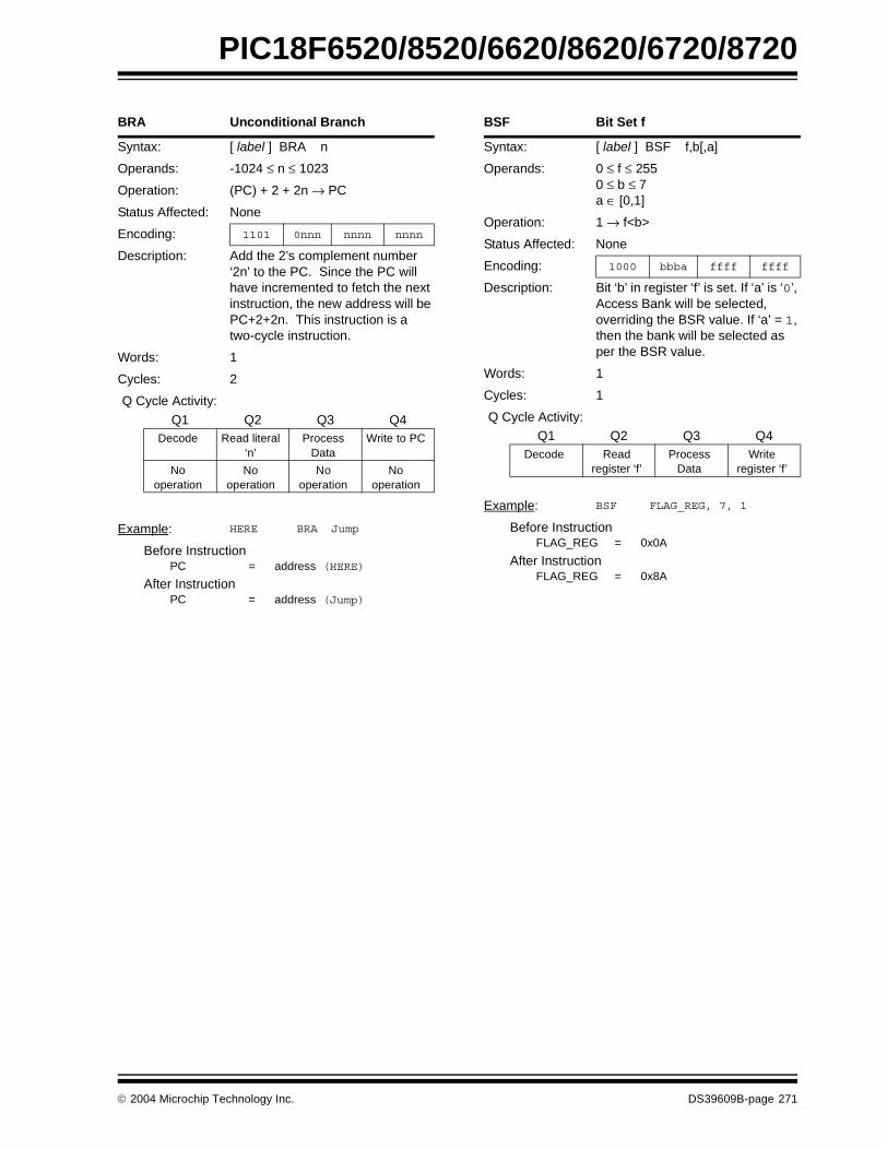
PIC18F6520/8520/6620/8620/6720/8720
BRA Unconditional Branch
Syntax: [ label ] BRA n
Operands: -1024 ≤ n ≤ 1023
Operation: (PC) + 2 + 2n → PC
Status Affected: None
Encoding: 1101 0nnn nnnn nnnn
Description: Add the 2’s complement number ‘2n’ to the PC. Since the PC will have incremented to fetch the next instruction, the new address will be PC+2+2n. This instruction is a two-cycle instruction.
Words: 1
Cycles: 2
Q Cycle Activity:
Q1 Q2 Q3 Q4Decode Read literal
‘n’Process
DataWrite to PC
No operation
No operation
No operation
No operation
Example: HERE BRA Jump
Before InstructionPC = address (HERE)
After InstructionPC = address (Jump)
BSF Bit Set f
Syntax: [ label ] BSF f,b[,a]
Operands: 0 ≤ f ≤ 2550 ≤ b ≤ 7a ∈ [0,1]
Operation: 1 → f<b>
Status Affected: None
Encoding: 1000 bbba ffff ffff
Description: Bit ‘b’ in register ‘f’ is set. If ‘a’ is ‘0’, Access Bank will be selected, overriding the BSR value. If ‘a’ = 1, then the bank will be selected as per the BSR value.
Words: 1
Cycles: 1
Q Cycle Activity:Q1 Q2 Q3 Q4
Decode Readregister ‘f’
Process Data
Writeregister ‘f’
Example: BSF FLAG_REG, 7, 1
Before InstructionFLAG_REG = 0x0A
After InstructionFLAG_REG = 0x8A
2004 Microchip Technology Inc. DS39609B-page 271

PIC18F6520/8520/6620/8620/6720/8720
BTFSC Bit Test File, Skip if Clear
Syntax: [ label ] BTFSC f,b[,a]
Operands: 0 ≤ f ≤ 2550 ≤ b ≤ 7a ∈ [0,1]
Operation: skip if (f<b>) = 0
Status Affected: None
Encoding: 1011 bbba ffff ffff
Description: If bit ‘b’ in register ‘f’ is ‘0’, then the next instruction is skipped.If bit ‘b’ is ‘0’, then the next instruction fetched during the current instruction execution is discarded and a NOP is executed instead, making this a two-cycle instruction. If ‘a’ is ‘0’, the Access Bank will be selected, overriding the BSR value. If ‘a’ = 1, then the bank will be selected as per the BSR value (default).
Words: 1
Cycles: 1(2)Note: 3 cycles if skip and followed
by a 2-word instruction.
Q Cycle Activity:
Q1 Q2 Q3 Q4Decode Read
register ‘f’Process
DataNo
operation
If skip:
Q1 Q2 Q3 Q4No
operationNo
operationNo
operationNo
operation
If skip and followed by 2-word instruction:
Q1 Q2 Q3 Q4No
operationNo
operationNo
operationNo
operation
No operation
No operation
No operation
No operation
Example: HEREFALSETRUE
BTFSC::
FLAG, 1, 0
Before InstructionPC = address (HERE)
After InstructionIf FLAG<1> = 0;
PC = address (TRUE)If FLAG<1> = 1;
PC = address (FALSE)
BTFSS Bit Test File, Skip if Set
Syntax: [ label ] BTFSS f,b[,a]
Operands: 0 ≤ f ≤ 2550 ≤ b < 7a ∈ [0,1]
Operation: skip if (f<b>) = 1
Status Affected: None
Encoding: 1010 bbba ffff ffff
Description: If bit ‘b’ in register ‘f’ is ‘1’, then the next instruction is skipped.If bit ‘b’ is ‘1’, then the next instruction fetched during the current instruction execution is discarded and a NOP is executed instead, making this a two-cycle instruction. If ‘a’ is ‘0’, the Access Bank will be selected, overriding the BSR value. If ‘a’ = 1, then the bank will be selected as per the BSR value (default).
Words: 1
Cycles: 1(2)Note: 3 cycles if skip and followed
by a 2-word instruction.
Q Cycle Activity:
Q1 Q2 Q3 Q4Decode Read
register ‘f’Process
DataNo
operation
If skip:
Q1 Q2 Q3 Q4No
operationNo
operationNo
operationNo
operation
If skip and followed by 2-word instruction:
Q1 Q2 Q3 Q4No
operationNo
operationNo
operationNo
operation
No operation
No operation
No operation
No operation
Example: HEREFALSETRUE
BTFSS::
FLAG, 1, 0
Before InstructionPC = address (HERE)
After InstructionIf FLAG<1> = 0;
PC = address (FALSE)If FLAG<1> = 1;
PC = address (TRUE)
DS39609B-page 272 2004 Microchip Technology Inc.
PIC18F6520/8520/6620/8620/6720/8720
BTG Bit Toggle f
Syntax: [ label ] BTG f,b[,a]
Operands: 0 ≤ f ≤ 2550 ≤ b < 7a ∈ [0,1]
Operation: (f<b>) → f<b>
Status Affected: None
Encoding: 0111 bbba ffff ffff
Description: Bit ‘b’ in data memory location ‘f’ is inverted. If ‘a’ is ‘0’, the Access Bank will be selected, overriding the BSR value. If ‘a’ = 1, then the bank will be selected as per the BSR value (default).
Words: 1
Cycles: 1
Q Cycle Activity:Q1 Q2 Q3 Q4
Decode Readregister ‘f’
Process Data
Writeregister ‘f’
Example: BTG PORTC, 4, 0
Before Instruction:PORTC = 0111 0101 [0x75]
After Instruction:PORTC = 0110 0101 [0x65]
BOV Branch if Overflow
Syntax: [ label ] BOV n
Operands: -128 ≤ n ≤ 127
Operation: if Overflow bit is ‘1’(PC) + 2 + 2n → PC
Status Affected: None
Encoding: 1110 0100 nnnn nnnn
Description: If the Overflow bit is ‘1’, then the program will branch.The 2’s complement number ‘2n’ is added to the PC. Since the PC will have incremented to fetch the next instruction, the new address will be PC+2+2n. This instruction is then a two-cycle instruction.
Words: 1
Cycles: 1(2)
Q Cycle Activity:If Jump:
Q1 Q2 Q3 Q4Decode Read literal
‘n’Process
DataWrite to PC
No operation
No operation
No operation
No operation
If No Jump:
Q1 Q2 Q3 Q4Decode Read literal
‘n’Process
DataNo
operation
Example: HERE BOV Jump
Before InstructionPC = address (HERE)
After InstructionIf Overflow = 1;
PC = address (Jump)If Overflow = 0;
PC = address (HERE+2)
2004 Microchip Technology Inc. DS39609B-page 273

PIC18F6520/8520/6620/8620/6720/8720
BZ Branch if Zero
Syntax: [ label ] BZ n
Operands: -128 ≤ n ≤ 127
Operation: if Zero bit is ‘1’(PC) + 2 + 2n → PC
Status Affected: None
Encoding: 1110 0000 nnnn nnnn
Description: If the Zero bit is ‘1’, then the program will branch.The 2’s complement number ‘2n’ is added to the PC. Since the PC will have incremented to fetch the next instruction, the new address will be PC+2+2n. This instruction is then a two-cycle instruction.
Words: 1
Cycles: 1(2)
Q Cycle Activity:If Jump:
Q1 Q2 Q3 Q4Decode Read literal
‘n’Process
DataWrite to PC
No operation
No operation
No operation
No operation
If No Jump:
Q1 Q2 Q3 Q4Decode Read literal
‘n’Process
DataNo
operation
Example: HERE BZ Jump
Before InstructionPC = address (HERE)
After InstructionIf Zero = 1;
PC = address (Jump)If Zero = 0;
PC = address (HERE+2)
CALL Subroutine Call
Syntax: [ label ] CALL k [,s]
Operands: 0 ≤ k ≤ 1048575s ∈ [0,1]
Operation: (PC) + 4 → TOS,k → PC<20:1>,if s = 1(W) → WS,(STATUS) → STATUSS,(BSR) → BSRS
Status Affected: None
Encoding:1st word (k<7:0>)2nd word(k<19:8>)
11101111
110sk19kkk
k7kkkkkkk
kkkk0kkkk8
Description: Subroutine call of entire 2-Mbyte memory range. First, return address (PC+ 4) is pushed onto the return stack. If ‘s’ = 1, the W, Status and BSR registers are also pushed into their respective shadow registers, WS, STATUSS and BSRS. If ‘s’ = 0, no update occurs (default). Then, the 20-bit value ‘k’ is loaded into PC<20:1>. CALL is a two-cycle instruction.
Words: 2
Cycles: 2
Q Cycle Activity:Q1 Q2 Q3 Q4
Decode Read literal ‘k’<7:0>
Push PC to stack
Read literal ‘k’<19:8>,
Write to PC
No operation
No operation
No operation
No operation
Example: HERE CALL THERE,1
Before InstructionPC = address (HERE)
After InstructionPC = address (THERE)TOS = address (HERE + 4)WS = WBSRS = BSRSTATUSS = STATUS
DS39609B-page 274 2004 Microchip Technology Inc.

PIC18F6520/8520/6620/8620/6720/8720
CLRF Clear f
Syntax: [ label ] CLRF f [,a]
Operands: 0 ≤ f ≤ 255a ∈ [0,1]
Operation: 000h → f1 → Z
Status Affected: Z
Encoding: 0110 101a ffff ffff
Description: Clears the contents of the specified register. If ‘a’ is ‘0’, the Access Bank will be selected, overriding the BSR value. If ‘a’ = 1, then the bank will be selected as per the BSR value (default).
Words: 1
Cycles: 1
Q Cycle Activity:Q1 Q2 Q3 Q4
Decode Readregister ‘f’
Process Data
Writeregister ‘f’
Example: CLRF FLAG_REG,1
Before InstructionFLAG_REG = 0x5A
After InstructionFLAG_REG = 0x00
CLRWDT Clear Watchdog Timer
Syntax: [ label ] CLRWDT
Operands: None
Operation: 000h → WDT,000h → WDT postscaler,1 → TO,1 → PD
Status Affected: TO, PD
Encoding: 0000 0000 0000 0100
Description: CLRWDT instruction resets the Watchdog Timer. It also resets the postscaler of the WDT. Status bits TO and PD are set.
Words: 1
Cycles: 1
Q Cycle Activity:Q1 Q2 Q3 Q4
Decode No operation
Process Data
No operation
Example: CLRWDT
Before InstructionWDT Counter = ?
After InstructionWDT Counter = 0x00WDT Postscaler = 0TO = 1PD = 1
2004 Microchip Technology Inc. DS39609B-page 275

PIC18F6520/8520/6620/8620/6720/8720
COMF Complement f
Syntax: [ label ] COMF f [,d [,a]
Operands: 0 ≤ f ≤ 255d ∈ [0,1]a ∈ [0,1]
Operation: → dest
Status Affected: N, Z
Encoding: 0001 11da ffff ffff
Description: The contents of register ‘f’ are com-plemented. If ‘d’ is ‘0’, the result is stored in W. If ‘d’ is ‘1’, the result is stored back in register ‘f’ (default). If ‘a’ is ‘0’, the Access Bank will be selected, overriding the BSR value. If ‘a’ = 1, then the bank will be selected as per the BSR value (default).
Words: 1
Cycles: 1
Q Cycle Activity:Q1 Q2 Q3 Q4
Decode Readregister ‘f’
Process Data
Write todestination
Example: COMF REG, 0, 0
Before InstructionREG = 0x13
After InstructionREG = 0x13W = 0xEC
( f )
CPFSEQ Compare f with W, skip if f = W
Syntax: [ label ] CPFSEQ f [,a]
Operands: 0 ≤ f ≤ 255a ∈ [0,1]
Operation: (f) – (W), skip if (f) = (W) (unsigned comparison)
Status Affected: None
Encoding: 0110 001a ffff ffff
Description: Compares the contents of data memory location ‘f’ to the contents of W by performing an unsigned subtraction.If ‘f’ = W, then the fetched instruction is discarded and a NOP is executed instead, making this a two-cycle instruction. If ‘a’ is ‘0’, the Access Bank will be selected, overriding the BSR value. If ‘a’ = 1, then the bank will be selected as per the BSR value (default).
Words: 1
Cycles: 1(2)Note: 3 cycles if skip and followed
by a 2-word instruction.
Q Cycle Activity:Q1 Q2 Q3 Q4
Decode Readregister ‘f’
Process Data
No operation
If skip:Q1 Q2 Q3 Q4No
operationNo
operationNo
operationNo
operation
If skip and followed by 2-word instruction:Q1 Q2 Q3 Q4No
operationNo
operationNo
operationNo
operation
No operation
No operation
No operation
No operation
Example: HERE CPFSEQ REG, 0NEQUAL :EQUAL :
Before InstructionPC Address = HERE
W = ?REG = ?
After InstructionIf REG = W;
PC = Address (EQUAL)If REG ≠ W;
PC = Address (NEQUAL)
DS39609B-page 276 2004 Microchip Technology Inc.

PIC18F6520/8520/6620/8620/6720/8720
CPFSGT Compare f with W, skip if f > W
Syntax: [ label ] CPFSGT f [,a]
Operands: 0 ≤ f ≤ 255a ∈ [0,1]
Operation: (f) − (W),skip if (f) > (W) (unsigned comparison)
Status Affected: None
Encoding: 0110 010a ffff ffff
Description: Compares the contents of data memory location ‘f’ to the contents of W by performing an unsigned subtraction.If the contents of ‘f’ are greater than the contents of WREG, then the fetched instruction is discarded and a NOP is executed instead, making this a two-cycle instruction. If ‘a’ is ‘0’, the Access Bank will be selected, overriding the BSR value. If ‘a’ = 1, then the bank will be selected as per the BSR value (default).
Words: 1
Cycles: 1(2)Note: 3 cycles if skip and followed
by a 2-word instruction.
Q Cycle Activity:Q1 Q2 Q3 Q4
Decode Readregister ‘f’
Process Data
No operation
If skip:Q1 Q2 Q3 Q4No
operationNo
operationNo
operationNo
operation
If skip and followed by 2-word instruction:Q1 Q2 Q3 Q4No
operationNo
operationNo
operationNo
operation
No operation
No operation
No operation
No operation
Example: HERE CPFSGT REG, 0NGREATER :GREATER :
Before InstructionPC = Address (HERE)W = ?
After InstructionIf REG > W;
PC = Address (GREATER)If REG ≤ W;
PC = Address (NGREATER)
CPFSLT Compare f with W, skip if f < W
Syntax: [ label ] CPFSLT f [,a]
Operands: 0 ≤ f ≤ 255a ∈ [0,1]
Operation: (f) – (W),skip if (f) < (W) (unsigned comparison)
Status Affected: None
Encoding: 0110 000a ffff ffff
Description: Compares the contents of data memory location ‘f’ to the contents of W by performing an unsigned subtraction.If the contents of ‘f’ are less than the contents of W, then the fetched instruction is discarded and a NOP is executed instead, making this a two-cycle instruction. If ‘a’ is ‘0’, the Access Bank will be selected. If ‘a’ is ‘1’, the BSR will not be overridden (default).
Words: 1
Cycles: 1(2)Note: 3 cycles if skip and followed
by a 2-word instruction.
Q Cycle Activity:Q1 Q2 Q3 Q4
Decode Readregister ‘f’
Process Data
No operation
If skip:Q1 Q2 Q3 Q4No
operationNo
operationNo
operationNo
operation
If skip and followed by 2-word instruction:Q1 Q2 Q3 Q4No
operationNo
operationNo
operationNo
operation
No operation
No operation
No operation
No operation
Example: HERE CPFSLT REG, 1NLESS :LESS :
Before InstructionPC = Address (HERE)W = ?
After InstructionIf REG < W;PC = Address (LESS)If REG ≥ W;PC = Address (NLESS)
2004 Microchip Technology Inc. DS39609B-page 277
PIC18F6520/8520/6620/8620/6720/8720
DAW Decimal Adjust W Register
Syntax: [ label ] DAW
Operands: None
Operation: If [W<3:0> >9] or [DC = 1] then(W<3:0>) + 6 → W<3:0>;else (W<3:0>) → W<3:0>;
If [W<7:4> >9] or [C = 1] then(W<7:4>) + 6 → W<7:4>;else (W<7:4>) → W<7:4>;
Status Affected: C
Encoding: 0000 0000 0000 0111
Description: DAW adjusts the eight-bit value in W, resulting from the earlier addition of two variables (each in packed BCD format) and produces a correct packed BCD result.
Words: 1
Cycles: 1
Q Cycle Activity:Q1 Q2 Q3 Q4
Decode Readregister W
Process Data
WriteW
Example1: DAW
Before InstructionW = 0xA5C = 0DC = 0
After InstructionW = 0x05C = 1DC = 0
Example 2:
Before InstructionW = 0xCEC = 0DC = 0
After InstructionW = 0x34C = 1DC = 0
DECF Decrement f
Syntax: [ label ] DECF f [,d [,a]
Operands: 0 ≤ f ≤ 255d ∈ [0,1]a ∈ [0,1]
Operation: (f) – 1 → dest
Status Affected: C, DC, N, OV, Z
Encoding: 0000 01da ffff ffff
Description: Decrement register ‘f’. If ‘d’ is ‘0’, the result is stored in W. If ‘d’ is ‘1’, the result is stored back in register ‘f’ (default). If ‘a’ is ‘0’, the Access Bank will be selected, overriding the BSR value. If ‘a’ = 1, then the bank will be selected as per the BSR value (default).
Words: 1
Cycles: 1
Q Cycle Activity:Q1 Q2 Q3 Q4
Decode Readregister ‘f’
Process Data
Write to destination
Example: DECF CNT, 1, 0
Before InstructionCNT = 0x01Z = 0
After InstructionCNT = 0x00Z = 1
DS39609B-page 278 2004 Microchip Technology Inc.

PIC18F6520/8520/6620/8620/6720/8720
DECFSZ Decrement f, skip if 0
Syntax: [ label ] DECFSZ f [,d [,a]]
Operands: 0 ≤ f ≤ 255d ∈ [0,1]a ∈ [0,1]
Operation: (f) – 1 → dest,skip if result = 0
Status Affected: None
Encoding: 0010 11da ffff ffff
Description: The contents of register ‘f’ are decremented. If ‘d’ is ‘0’, the result is placed in W. If ‘d’ is ‘1’, the result is placed back in register ‘f’ (default).If the result is ‘0’, the next instruction which is already fetched is discarded and a NOP is executed instead, making it a two-cycle instruction. If ‘a’ is ‘0’, the Access Bank will be selected, overriding the BSR value. If ‘a’ = 1, then the bank will be selected as per the BSR value (default).
Words: 1
Cycles: 1(2)Note: 3 cycles if skip and followed
by a 2-word instruction.
Q Cycle Activity:Q1 Q2 Q3 Q4
Decode Readregister ‘f’
Process Data
Write to destination
If skip:Q1 Q2 Q3 Q4No
operationNo
operationNo
operationNo
operation
If skip and followed by 2-word instruction:Q1 Q2 Q3 Q4No
operationNo
operationNo
operationNo
operation
No operation
No operation
No operation
No operation
Example: HERE DECFSZ CNT, 1, 1 GOTO LOOPCONTINUE
Before InstructionPC = Address (HERE)
After InstructionCNT = CNT - 1If CNT = 0;
PC = Address (CONTINUE)If CNT ≠ 0;
PC = Address (HERE+2)
DCFSNZ Decrement f, skip if not 0
Syntax: [ label ] DCFSNZ f [,d [,a]
Operands: 0 ≤ f ≤ 255d ∈ [0,1]a ∈ [0,1]
Operation: (f) – 1 → dest,skip if result ≠ 0
Status Affected: None
Encoding: 0100 11da ffff ffff
Description: The contents of register ‘f’ are decremented. If ‘d’ is ‘0’, the result is placed in W. If ‘d’ is ‘1’, the result is placed back in register ‘f’ (default).If the result is not ‘0’, the next instruction which is already fetched is discarded and a NOP is executed instead, making it a two-cycle instruction. If ‘a’ is ‘0’, the Access Bank will be selected, overriding the BSR value. If ‘a’ = 1, then the bank will be selected as per the BSR value (default).
Words: 1
Cycles: 1(2)Note: 3 cycles if skip and followed
by a 2-word instruction.
Q Cycle Activity:Q1 Q2 Q3 Q4
Decode Readregister ‘f’
Process Data
Write to destination
If skip:Q1 Q2 Q3 Q4No
operationNo
operationNo
operationNo
operation
If skip and followed by 2-word instruction:Q1 Q2 Q3 Q4No
operationNo
operationNo
operationNo
operation
No operation
No operation
No operation
No operation
Example: HERE DCFSNZ TEMP, 1, 0ZERO : NZERO :
Before InstructionTEMP = ?
After InstructionTEMP = TEMP - 1,If TEMP = 0;
PC = Address (ZERO)If TEMP ≠ 0;
PC = Address (NZERO)
2004 Microchip Technology Inc. DS39609B-page 279

PIC18F6520/8520/6620/8620/6720/8720
GOTO Unconditional Branch
Syntax: [ label ] GOTO k
Operands: 0 ≤ k ≤ 1048575
Operation: k → PC<20:1>
Status Affected: None
Encoding:1st word (k<7:0>)2nd word(k<19:8>)
11101111
1111k19kkk
k7kkkkkkk
kkkk0kkkk8
Description: GOTO allows an unconditional branch anywhere within the entire 2-Mbyte memory range. The 20-bit value ‘k’ is loaded into PC<20:1>. GOTO is always a two-cycle instruction.
Words: 2
Cycles: 2
Q Cycle Activity:Q1 Q2 Q3 Q4
Decode Read literal ‘k’<7:0>
No operation
Read literal ’k’<19:8>,
Write to PC
No operation
No operation
No operation
No operation
Example: GOTO THERE
After InstructionPC = Address (THERE)
INCF Increment f
Syntax: [ label ] INCF f [,d [,a]
Operands: 0 ≤ f ≤ 255d ∈ [0,1]a ∈ [0,1]
Operation: (f) + 1 → dest
Status Affected: C, DC, N, OV, Z
Encoding: 0010 10da ffff ffff
Description: The contents of register ‘f’ are incremented. If ‘d’ is ‘0’, the result is placed in W. If ‘d’ is ‘1’, the result is placed back in register ‘f’ (default). If ‘a’ is ‘0’, the Access Bank will be selected, overriding the BSR value. If ‘a’ = 1, then the bank will be selected as per the BSR value (default).
Words: 1
Cycles: 1
Q Cycle Activity:Q1 Q2 Q3 Q4
Decode Readregister ‘f’
Process Data
Write to destination
Example: INCF CNT, 1, 0
Before InstructionCNT = 0xFFZ = 0C = ?DC = ?
After InstructionCNT = 0x00Z = 1C = 1DC = 1
DS39609B-page 280 2004 Microchip Technology Inc.

PIC18F6520/8520/6620/8620/6720/8720
INCFSZ Increment f, skip if 0
Syntax: [ label ] INCFSZ f [,d [,a]
Operands: 0 ≤ f ≤ 255d ∈ [0,1]a ∈ [0,1]
Operation: (f) + 1 → dest,skip if result = 0
Status Affected: None
Encoding: 0011 11da ffff ffff
Description: The contents of register ‘f’ are incremented. If ‘d’ is ‘0’, the result is placed in W. If ‘d’ is ‘1’, the result is placed back in register ‘f’ (default).If the result is ‘0’, the next instruction which is already fetched is discarded and a NOP is executed instead, making it a two-cycle instruction. If ‘a’ is ‘0’, the Access Bank will be selected, overriding the BSR value. If ‘a’ = 1, then the bank will be selected as per the BSR value (default).
Words: 1
Cycles: 1(2)Note: 3 cycles if skip and followed
by a 2-word instruction.
Q Cycle Activity:Q1 Q2 Q3 Q4
Decode Readregister ‘f’
Process Data
Write to destination
If skip:Q1 Q2 Q3 Q4No
operationNo
operationNo
operationNo
operation
If skip and followed by 2-word instruction:Q1 Q2 Q3 Q4No
operationNo
operationNo
operationNo
operation
No operation
No operation
No operation
No operation
Example: HERE INCFSZ CNT, 1, 0NZERO : ZERO :
Before InstructionPC = Address (HERE)
After InstructionCNT = CNT + 1If CNT = 0;PC = Address (ZERO)If CNT ≠ 0;PC = Address (NZERO)
INFSNZ Increment f, skip if not 0
Syntax: [ label ] INFSNZ f [,d [,a]
Operands: 0 ≤ f ≤ 255d ∈ [0,1]a ∈ [0,1]
Operation: (f) + 1 → dest, skip if result ≠ 0
Status Affected: None
Encoding: 0100 10da ffff ffff
Description: The contents of register ‘f’ are incremented. If ‘d’ is ‘0’, the result is placed in W. If ‘d’ is ‘1’, the result is placed back in register ‘f’ (default).If the result is not ‘0’, the next instruction which is already fetched is discarded and a NOP is executed instead, making it a two-cycle instruction. If ‘a’ is ‘0’, the Access Bank will be selected, overriding the BSR value. If ‘a’ = 1, then the bank will be selected as per the BSR value (default).
Words: 1
Cycles: 1(2)Note: 3 cycles if skip and followed
by a 2-word instruction.
Q Cycle Activity:Q1 Q2 Q3 Q4
Decode Readregister ‘f’
Process Data
Write to destination
If skip:Q1 Q2 Q3 Q4No
operationNo
operationNo
operationNo
operation
If skip and followed by 2-word instruction:Q1 Q2 Q3 Q4No
operationNo
operationNo
operationNo
operation
No operation
No operation
No operation
No operation
Example: HERE INFSNZ REG, 1, 0ZERONZERO
Before InstructionPC = Address (HERE)
After InstructionREG = REG + 1If REG ≠ 0;PC = Address (NZERO)If REG = 0;PC = Address (ZERO)
2004 Microchip Technology Inc. DS39609B-page 281

PIC18F6520/8520/6620/8620/6720/8720
IORLW Inclusive OR literal with W
Syntax: [ label ] IORLW k
Operands: 0 ≤ k ≤ 255
Operation: (W) .OR. k → W
Status Affected: N, Z
Encoding: 0000 1001 kkkk kkkk
Description: The contents of W are OR’ed with the eight-bit literal ‘k’. The result is placed in W.
Words: 1
Cycles: 1
Q Cycle Activity:
Q1 Q2 Q3 Q4Decode Read
literal ‘k’Process
DataWrite to W
Example: IORLW 0x35
Before InstructionW = 0x9A
After InstructionW = 0xBF
IORWF Inclusive OR W with f
Syntax: [ label ] IORWF f [,d [,a]
Operands: 0 ≤ f ≤ 255d ∈ [0,1]a ∈ [0,1]
Operation: (W) .OR. (f) → dest
Status Affected: N, Z
Encoding: 0001 00da ffff ffff
Description: Inclusive OR W with register ‘f’. If ‘d’ is ‘0’, the result is placed in W. If ‘d’ is ‘1’, the result is placed back in register ‘f’ (default). If ‘a’ is ‘0’, the Access Bank will be selected, over-riding the BSR value. If ‘a’ = 1, then the bank will be selected as per the BSR value (default).
Words: 1
Cycles: 1
Q Cycle Activity:Q1 Q2 Q3 Q4
Decode Readregister ‘f’
Process Data
Write to destination
Example: IORWF RESULT, 0, 1
Before InstructionRESULT = 0x13W = 0x91
After InstructionRESULT = 0x13W = 0x93
DS39609B-page 282 2004 Microchip Technology Inc.

PIC18F6520/8520/6620/8620/6720/8720
LFSR Load FSR
Syntax: [ label ] LFSR f,k
Operands: 0 ≤ f ≤ 20 ≤ k ≤ 4095
Operation: k → FSRf
Status Affected: None
Encoding: 11101111
11100000
00ffk7kkk
k11kkkkkkk
Description: The 12-bit literal ‘k’ is loaded into the File Select Register pointed to by ‘f’.
Words: 2
Cycles: 2
Q Cycle Activity:Q1 Q2 Q3 Q4
Decode Read literal ‘k’ MSB
Process Data
Write literal ‘k’ MSB to
FSRfH
Decode Read literal ‘k’ LSB
Process Data
Write literal ‘k’ to FSRfL
Example: LFSR 2, 0x3AB
After InstructionFSR2H = 0x03FSR2L = 0xAB
MOVF Move f
Syntax: [ label ] MOVF f [,d [,a]
Operands: 0 ≤ f ≤ 255d ∈ [0,1]a ∈ [0,1]
Operation: f → dest
Status Affected: N, Z
Encoding: 0101 00da ffff ffff
Description: The contents of register ‘f’ are moved to a destination dependent upon the status of ‘d’. If ‘d’ is ‘0’, the result is placed in W. If ‘d’ is ‘1’, the result is placed back in register ‘f’ (default). Location ‘f’ can be anywhere in the 256-byte bank. If ‘a’ is ‘0’, the Access Bank will be selected, overriding the BSR value. If ‘a’ = 1, then the bank will be selected as per the BSR value (default).
Words: 1
Cycles: 1
Q Cycle Activity:Q1 Q2 Q3 Q4
Decode Readregister ‘f’
Process Data
Write W
Example: MOVF REG, 0, 0
Before InstructionREG = 0x22W = 0xFF
After InstructionREG = 0x22W = 0x22
2004 Microchip Technology Inc. DS39609B-page 283

PIC18F6520/8520/6620/8620/6720/8720
MOVFF Move f to f
Syntax: [ label ] MOVFF fs,fdOperands: 0 ≤ fs ≤ 4095
0 ≤ fd ≤ 4095
Operation: (fs) → fdStatus Affected: None
Encoding:1st word (source)2nd word (destin.)
11001111
ffffffff
ffffffff
ffffsffffd
Description: The contents of source register ‘fs’ are moved to destination register ‘fd’. Location of source ‘fs’ can be anywhere in the 4096-byte data space (000h to FFFh) and location of destination ‘fd’ can also be anywhere from 000h to FFFh.Either source or destination can be W (a useful special situation).MOVFF is particularly useful for transferring a data memory location to a peripheral register (such as the transmit buffer or an I/O port).The MOVFF instruction cannot use the PCL, TOSU, TOSH or TOSL as the destination register.
Words: 2
Cycles: 2 (3)
Q Cycle Activity:Q1 Q2 Q3 Q4
Decode Readregister ‘f’
(src)
Process Data
No operation
Decode No operation,
No dummy read
No operation
Write register ‘f’
(dest)
Example: MOVFF REG1, REG2
Before InstructionREG1 = 0x33REG2 = 0x11
After InstructionREG1 = 0x33,REG2 = 0x33
MOVLB Move literal to low nibble in BSR
Syntax: [ label ] MOVLB k
Operands: 0 ≤ k ≤ 255
Operation: k → BSR
Status Affected: None
Encoding: 0000 0001 kkkk kkkk
Description: The 8-bit literal ‘k’ is loaded into the Bank Select Register (BSR).
Words: 1
Cycles: 1
Q Cycle Activity:Q1 Q2 Q3 Q4
Decode Read literal ‘k’
Process Data
Writeliteral ‘k’ to
BSR
Example: MOVLB 5
Before InstructionBSR register = 0x02
After InstructionBSR register = 0x05
DS39609B-page 284 2004 Microchip Technology Inc.
PIC18F6520/8520/6620/8620/6720/8720
MOVLW Move literal to W
Syntax: [ label ] MOVLW k
Operands: 0 ≤ k ≤ 255
Operation: k → W
Status Affected: None
Encoding: 0000 1110 kkkk kkkk
Description: The eight-bit literal ‘k’ is loaded into W.
Words: 1
Cycles: 1
Q Cycle Activity:Q1 Q2 Q3 Q4
Decode Readliteral ‘k’
Process Data
Write to W
Example: MOVLW 0x5A
After InstructionW = 0x5A
MOVWF Move W to f
Syntax: [ label ] MOVWF f [,a]
Operands: 0 ≤ f ≤ 255a ∈ [0,1]
Operation: (W) → f
Status Affected: None
Encoding: 0110 111a ffff ffff
Description: Move data from W to register ‘f’. Location ‘f’ can be anywhere in the 256-byte bank. If ‘a’ is ‘0’, the Access Bank will be selected, overriding the BSR value. If ‘a’ = 1, then the bank will be selected as per the BSR value (default).
Words: 1
Cycles: 1
Q Cycle Activity:Q1 Q2 Q3 Q4
Decode Readregister ‘f’
Process Data
Writeregister ‘f’
Example: MOVWF REG, 0
Before InstructionW = 0x4FREG = 0xFF
After InstructionW = 0x4FREG = 0x4F
2004 Microchip Technology Inc. DS39609B-page 285

PIC18F6520/8520/6620/8620/6720/8720
MULLW Multiply Literal with W
Syntax: [ label ] MULLW k
Operands: 0 ≤ k ≤ 255
Operation: (W) x k → PRODH:PRODL
Status Affected: None
Encoding: 0000 1101 kkkk kkkk
Description: An unsigned multiplication is carried out between the contents of W and the 8-bit literal ‘k’. The 16-bit result is placed in PRODH:PRODL register pair. PRODH contains the high byte.W is unchanged.None of the status flags are affected.Note that neither overflow nor carry is possible in this operation. A zero result is possible but not detected.
Words: 1
Cycles: 1
Q Cycle Activity:Q1 Q2 Q3 Q4
Decode Read literal ‘k’
Process Data
Write registers PRODH:PRODL
Example: MULLW 0xC4
Before InstructionW = 0xE2PRODH = ?PRODL = ?
After Instruction
W = 0xE2PRODH = 0xADPRODL = 0x08
MULWF Multiply W with f
Syntax: [ label ] MULWF f [,a]
Operands: 0 ≤ f ≤ 255a ∈ [0,1]
Operation: (W) x (f) → PRODH:PRODL
Status Affected: None
Encoding: 0000 001a ffff ffff
Description An unsigned multiplication is carried out between the contents of W and the register file location ‘f’. The 16-bit result is stored in the PRODH:PRODL register pair. PRODH contains the high byte.Both W and ‘f’ are unchanged.None of the status flags are affected.Note that neither overflow nor carry is possible in this operation. A zero result is possible but not detected. If ‘a’ is ‘0’, the Access Bank will be selected, overriding the BSR value. If ‘a’= 1, then the bank will be selected as per the BSR value (default).
Words: 1
Cycles: 1
Q Cycle Activity:Q1 Q2 Q3 Q4
Decode Readregister ‘f’
Process Data
Writeregisters PRODH:PRODL
Example: MULWF REG, 1
Before InstructionW = 0xC4REG = 0xB5PRODH = ?PRODL = ?
After InstructionW = 0xC4REG = 0xB5PRODH = 0x8APRODL = 0x94
DS39609B-page 286 2004 Microchip Technology Inc.

PIC18F6520/8520/6620/8620/6720/8720
NEGF Negate f
Syntax: [ label ] NEGF f [,a]
Operands: 0 ≤ f ≤ 255a ∈ [0,1]
Operation: ( f ) + 1 → f
Status Affected: N, OV, C, DC, Z
Encoding: 0110 110a ffff ffff
Description: Location ‘f’ is negated using two’s complement. The result is placed in the data memory location ‘f’. If ‘a’ is ‘0’, the Access Bank will be selected, overriding the BSR value. If ‘a’ = 1, then the bank will be selected as per the BSR value.
Words: 1
Cycles: 1
Q Cycle Activity:Q1 Q2 Q3 Q4
Decode Readregister ‘f’
Process Data
Write register ‘f’
Example: NEGF REG, 1
Before InstructionREG = 0011 1010 [0x3A]
After InstructionREG = 1100 0110 [0xC6]
NOP No Operation
Syntax: [ label ] NOP
Operands: None
Operation: No operation
Status Affected: None
Encoding: 00001111
0000xxxx
0000xxxx
0000xxxx
Description: No operation.
Words: 1
Cycles: 1
Q Cycle Activity:Q1 Q2 Q3 Q4
Decode No operation
No operation
No operation
Example:
None.
2004 Microchip Technology Inc. DS39609B-page 287
PIC18F6520/8520/6620/8620/6720/8720
POP Pop Top of Return Stack
Syntax: [ label ] POP
Operands: None
Operation: (TOS) → bit bucket
Status Affected: None
Encoding: 0000 0000 0000 0110
Description: The TOS value is pulled off the return stack and is discarded. The TOS value then becomes the previous value that was pushed onto the return stack.This instruction is provided to enable the user to properly manage the return stack to incorporate a software stack.
Words: 1
Cycles: 1
Q Cycle Activity:Q1 Q2 Q3 Q4
Decode Nooperation
POP TOS value
Nooperation
Example: POPGOTO NEW
Before InstructionTOS = 0031A2hStack (1 level down) = 014332h
After InstructionTOS = 014332hPC = NEW
PUSH Push Top of Return Stack
Syntax: [ label ] PUSH
Operands: None
Operation: (PC+2) → TOS
Status Affected: None
Encoding: 0000 0000 0000 0101
Description: The PC+2 is pushed onto the top of the return stack. The previous TOS value is pushed down on the stack.This instruction allows implementing a software stack by modifying TOS and then pushing it onto the return stack.
Words: 1
Cycles: 1
Q Cycle Activity:Q1 Q2 Q3 Q4
Decode PUSH PC+2 onto return
stack
No operation
No operation
Example: PUSH
Before InstructionTOS = 00345AhPC = 000124h
After InstructionPC = 000126hTOS = 000126hStack (1 level down) = 00345Ah
DS39609B-page 288 2004 Microchip Technology Inc.

PIC18F6520/8520/6620/8620/6720/8720
RCALL Relative Call
Syntax: [ label ] RCALL n
Operands: -1024 ≤ n ≤ 1023
Operation: (PC) + 2 → TOS,(PC) + 2 + 2n → PC
Status Affected: None
Encoding: 1101 1nnn nnnn nnnn
Description: Subroutine call with a jump up to 1K from the current location. First, return address (PC+2) is pushed onto the stack. Then, add the 2’s complement number ‘2n’ to the PC. Since the PC will have incremented to fetch the next instruction, the new address will be PC+2+2n. This instruction is a two-cycle instruction.
Words: 1
Cycles: 2
Q Cycle Activity:Q1 Q2 Q3 Q4
Decode Read literal ‘n’
Push PC to stack
Process Data
Write to PC
No operation
No operation
No operation
No operation
Example: HERE RCALL Jump
Before InstructionPC = Address (HERE)
After InstructionPC = Address (Jump)TOS = Address (HERE+2)
RESET Reset
Syntax: [ label ] RESET
Operands: None
Operation: Reset all registers and flags that are affected by a MCLR Reset.
Status Affected: All
Encoding: 0000 0000 1111 1111
Description: This instruction provides a way to execute a MCLR Reset in software.
Words: 1
Cycles: 1
Q Cycle Activity:
Q1 Q2 Q3 Q4Decode Start
ResetNo
operationNo
operation
Example: RESET
After InstructionRegisters = Reset ValueFlags* = Reset Value
2004 Microchip Technology Inc. DS39609B-page 289

PIC18F6520/8520/6620/8620/6720/8720
RETFIE Return from Interrupt
Syntax: [ label ] RETFIE [s]
Operands: s ∈ [0,1]
Operation: (TOS) → PC,1 → GIE/GIEH or PEIE/GIEL,if s = 1(WS) → W,(STATUSS) → STATUS,(BSRS) → BSR,PCLATU, PCLATH are unchanged
Status Affected: GIE/GIEH, PEIE/GIEL.
Encoding: 0000 0000 0001 000s
Description: Return from Interrupt. Stack is popped and Top-of-Stack (TOS) is loaded into the PC. Interrupts are enabled by setting either the high or low priority global interrupt enable bit. If ‘s’ = 1, the contents of the shadow registers, WS, STATUSS and BSRS, are loaded into their corresponding registers, W, Status and BSR. If ‘s’ = 0, no update of these registers occurs (default).
Words: 1
Cycles: 2
Q Cycle Activity:
Q1 Q2 Q3 Q4Decode No
operationNo
operationPop PC
from stack
Set GIEH or GIEL
No operation
No operation
No operation
No operation
Example: RETFIE 1
After InterruptPC = TOSW = WSBSR = BSRSSTATUS = STATUSSGIE/GIEH, PEIE/GIEL = 1
RETLW Return Literal to W
Syntax: [ label ] RETLW k
Operands: 0 ≤ k ≤ 255
Operation: k → W,(TOS) → PC,PCLATU, PCLATH are unchanged
Status Affected: None
Encoding: 0000 1100 kkkk kkkk
Description: W is loaded with the eight-bit literal ‘k’. The program counter is loaded from the top of the stack (the return address). The high address latch (PCLATH) remains unchanged.
Words: 1
Cycles: 2
Q Cycle Activity:Q1 Q2 Q3 Q4
Decode Readliteral ‘k’
Process Data
Pop PC from stack, Write to W
No operation
No operation
No operation
No operation
Example: CALL TABLE ; W contains table ; offset value ; W now has ; table value :TABLE
ADDWF PCL ; W = offsetRETLW k0 ; Begin tableRETLW k1 ;
: :
RETLW kn ; End of table
Before InstructionW = 0x07
After InstructionW = value of kn
DS39609B-page 290 2004 Microchip Technology Inc.

PIC18F6520/8520/6620/8620/6720/8720
RETURN Return from Subroutine
Syntax: [ label ] RETURN [s]
Operands: s ∈ [0,1]
Operation: (TOS) → PC,if s = 1(WS) → W,(STATUSS) → STATUS,(BSRS) → BSR,PCLATU, PCLATH are unchanged
Status Affected: None
Encoding: 0000 0000 0001 001s
Description: Return from subroutine. The stack is popped and the top of the stack (TOS) is loaded into the program counter. If ‘s’ = 1, the contents of the shadow registers, WS, STATUSS and BSRS, are loaded into their corresponding registers, W, Status and BSR. If ‘s’ = 0, no update of these registers occurs (default).
Words: 1
Cycles: 2
Q Cycle Activity:
Q1 Q2 Q3 Q4Decode No
operationProcess
DataPop PC
from stack
No operation
No operation
No operation
No operation
Example: RETURN
After InterruptPC = TOS
RLCF Rotate Left f through Carry
Syntax: [ label ] RLCF f [,d [,a]
Operands: 0 ≤ f ≤ 255d ∈ [0,1]a ∈ [0,1]
Operation: (f<n>) → dest<n+1>,(f<7>) → C,(C) → dest<0>
Status Affected: C, N, Z
Encoding: 0011 01da ffff ffff
Description: The contents of register ‘f’ are rotated one bit to the left through the Carry flag. If ‘d’ is ‘0’, the result is placed in W. If ‘d’ is ‘1’, the result is stored back in register ‘f’ (default). If ‘a’ is ‘0’, the Access Bank will be selected, overriding the BSR value. If ‘a’ = 1, then the bank will be selected as per the BSR value (default).
Words: 1
Cycles: 1
Q Cycle Activity:
Q1 Q2 Q3 Q4Decode Read
register ‘f’Process
DataWrite to
destination
Example: RLCF REG, 0, 0
Before InstructionREG = 1110 0110C = 0
After InstructionREG = 1110 0110W = 1100 1100C = 1
C register f
2004 Microchip Technology Inc. DS39609B-page 291

PIC18F6520/8520/6620/8620/6720/8720
RLNCF Rotate Left f (no carry)
Syntax: [ label ] RLNCF f [,d [,a]
Operands: 0 ≤ f ≤ 255d ∈ [0,1]a ∈ [0,1]
Operation: (f<n>) → dest<n+1>,(f<7>) → dest<0>
Status Affected: N, Z
Encoding: 0100 01da ffff ffff
Description: The contents of register ‘f’ are rotated one bit to the left. If ‘d’ is ‘0’, the result is placed in W. If ‘d’ is ‘1’, the result is stored back in register ‘f’ (default). If ‘a’ is ‘0’, the Access Bank will be selected, overriding the BSR value. If ‘a’ is ‘1’, then the bank will be selected as per the BSR value (default).
Words: 1
Cycles: 1
Q Cycle Activity:Q1 Q2 Q3 Q4
Decode Readregister ‘f’
Process Data
Write to destination
Example: RLNCF REG, 1, 0
Before InstructionREG = 1010 1011
After InstructionREG = 0101 0111
register f
RRCF Rotate Right f through Carry
Syntax: [ label ] RRCF f [,d [,a]
Operands: 0 ≤ f ≤ 255d ∈ [0,1]a ∈ [0,1]
Operation: (f<n>) → dest<n-1>,(f<0>) → C,(C) → dest<7>
Status Affected: C, N, Z
Encoding: 0011 00da ffff ffff
Description: The contents of register ‘f’ are rotated one bit to the right through the Carry flag. If ‘d’ is ‘0’, the result is placed in W. If ‘d’ is ‘1’, the result is placed back in register ‘f’ (default). If ‘a’ is ‘0’, the Access Bank will be selected, overriding the BSR value. If ‘a’ is ‘1’, then the bank will be selected as per the BSR value (default).
Words: 1
Cycles: 1
Q Cycle Activity:
Q1 Q2 Q3 Q4Decode Read
register ‘f’Process
DataWrite to
destination
Example: RRCF REG, 0, 0
Before InstructionREG = 1110 0110C = 0
After InstructionREG = 1110 0110W = 0111 0011C = 0
C register f
DS39609B-page 292 2004 Microchip Technology Inc.

PIC18F6520/8520/6620/8620/6720/8720
RRNCF Rotate Right f (no carry)
Syntax: [ label ] RRNCF f [,d [,a]
Operands: 0 ≤ f ≤ 255d ∈ [0,1]a ∈ [0,1]
Operation: (f<n>) → dest<n-1>,(f<0>) → dest<7>
Status Affected: N, Z
Encoding: 0100 00da ffff ffff
Description: The contents of register ‘f’ are rotated one bit to the right. If ‘d’ is ‘0’, the result is placed in W. If ‘d’ is ‘1’, the result is placed back in register ‘f’ (default). If ‘a’ is ‘0’, the Access Bank will be selected, overriding the BSR value. If ‘a’ is ‘1’, then the bank will be selected as per the BSR value (default).
Words: 1
Cycles: 1
Q Cycle Activity:Q1 Q2 Q3 Q4
Decode Readregister ‘f’
Process Data
Write to destination
Example 1: RRNCF REG, 1, 0
Before InstructionREG = 1101 0111
After InstructionREG = 1110 1011
Example 2: RRNCF REG, 0, 0
Before InstructionW = ?REG = 1101 0111
After InstructionW = 1110 1011REG = 1101 0111
register f
SETF Set f
Syntax: [ label ] SETF f [,a]
Operands: 0 ≤ f ≤ 255a ∈ [0,1]
Operation: FFh → f
Status Affected: None
Encoding: 0110 100a ffff ffff
Description: The contents of the specified register are set to FFh. If ‘a’ is ‘0’, the Access Bank will be selected, overriding the BSR value. If ‘a’ is ‘1’, then the bank will be selected as per the BSR value (default).
Words: 1
Cycles: 1
Q Cycle Activity:Q1 Q2 Q3 Q4
Decode Readregister ‘f’
Process Data
Writeregister ‘f’
Example: SETF REG,1
Before InstructionREG = 0x5A
After InstructionREG = 0xFF
2004 Microchip Technology Inc. DS39609B-page 293

PIC18F6520/8520/6620/8620/6720/8720
SLEEP Enter SLEEP mode
Syntax: [ label ] SLEEP
Operands: None
Operation: 00h → WDT,0 → WDT postscaler,1 → TO,0 → PD
Status Affected: TO, PD
Encoding: 0000 0000 0000 0011
Description: The Power-down status bit (PD) is cleared. The Time-out status bit (TO) is set. Watchdog Timer and its postscaler are cleared.The processor is put into Sleep mode with the oscillator stopped.
Words: 1
Cycles: 1
Q Cycle Activity:Q1 Q2 Q3 Q4
Decode No operation
Process Data
Go toSleep
Example: SLEEP
Before InstructionTO = ?PD = ?
After InstructionTO = 1 †PD = 0
† If WDT causes wake-up, this bit is cleared.
SUBFWB Subtract f from W with borrow
Syntax: [ label ] SUBFWB f [,d [,a]
Operands: 0 ≤ f ≤ 255d ∈ [0,1]a ∈ [0,1]
Operation: (W) – (f) – (C) → dest
Status Affected: N, OV, C, DC, Z
Encoding: 0101 01da ffff ffff
Description: Subtract register ‘f’ and Carry flag (borrow) from W (2’s complement method). If ‘d’ is ‘0’, the result is stored in W. If ‘d’ is ‘1’, the result is stored in register ‘f’ (default). If ‘a’ is ‘0’, the Access Bank will be selected, overriding the BSR value. If ‘a’ is ‘1’, then the bank will be selected as per the BSR value (default).
Words: 1
Cycles: 1
Q Cycle Activity:Q1 Q2 Q3 Q4
Decode Readregister ‘f’
Process Data
Write to destination
Example 1: SUBFWB REG, 1, 0
Before InstructionREG = 3W = 2C = 1
After InstructionREG = FFW = 2C = 0Z = 0N = 1 ; result is negative
Example 2: SUBFWB REG, 0, 0
Before InstructionREG = 2W = 5C = 1
After InstructionREG = 2W = 3C = 1Z = 0N = 0 ; result is positive
Example 3: SUBFWB REG, 1, 0
Before InstructionREG = 1W = 2C = 0
After InstructionREG = 0W = 2C = 1Z = 1 ; result is zeroN = 0
DS39609B-page 294 2004 Microchip Technology Inc.

PIC18F6520/8520/6620/8620/6720/8720
SUBLW Subtract W from literal
Syntax: [ label ] SUBLW k
Operands: 0 ≤ k ≤ 255
Operation: k – (W) → W
Status Affected: N, OV, C, DC, Z
Encoding: 0000 1000 kkkk kkkk
Description: W is subtracted from the eight-bit literal ‘k’. The result is placed in W.
Words: 1
Cycles: 1
Q Cycle Activity:Q1 Q2 Q3 Q4
Decode Readliteral ‘k’
Process Data
Write to W
Example 1: SUBLW 0x02
Before InstructionW = 1C = ?
After InstructionW = 1C = 1 ; result is positiveZ = 0N = 0
Example 2: SUBLW 0x02
Before InstructionW = 2C = ?
After InstructionW = 0C = 1 ; result is zeroZ = 1N = 0
Example 3: SUBLW 0x02
Before InstructionW = 3C = ?
After InstructionW = FF ; (2’s complement)C = 0 ; result is negativeZ = 0N = 1
SUBWF Subtract W from f
Syntax: [ label ] SUBWF f [,d [,a]
Operands: 0 ≤ f ≤ 255d ∈ [0,1]a ∈ [0,1]
Operation: (f) – (W) → dest
Status Affected: N, OV, C, DC, Z
Encoding: 0101 11da ffff ffff
Description: Subtract W from register ‘f’ (2’s complement method). If ‘d’ is ‘0’, the result is stored in W. If ‘d’ is ‘1’, the result is stored back in register ‘f’ (default). If ‘a’ is ‘0’, the Access Bank will be selected, overriding the BSR value. If ‘a’ is ‘1’, then the bank will be selected as per the BSR value (default).
Words: 1
Cycles: 1
Q Cycle Activity:
Q1 Q2 Q3 Q4Decode Read
register ‘f’Process
DataWrite to
destination
Example 1: SUBWF REG, 1, 0
Before InstructionREG = 3W = 2C = ?
After InstructionREG = 1W = 2C = 1 ; result is positiveZ = 0N = 0
Example 2: SUBWF REG, 0, 0
Before InstructionREG = 2W = 2C = ?
After InstructionREG = 2W = 0C = 1 ; result is zeroZ = 1N = 0
Example 3: SUBWF REG, 1, 0
Before InstructionREG = 1W = 2C = ?
After InstructionREG = FFh ;(2’s complement)W = 2C = 0 ; result is negativeZ = 0N = 1
2004 Microchip Technology Inc. DS39609B-page 295

PIC18F6520/8520/6620/8620/6720/8720
SUBWFB Subtract W from f with Borrow
Syntax: [ label ] SUBWFB f [,d [,a]
Operands: 0 ≤ f ≤ 255d ∈ [0,1]a ∈ [0,1]
Operation: (f) – (W) – (C) → dest
Status Affected: N, OV, C, DC, Z
Encoding: 0101 10da ffff ffff
Description: Subtract W and the Carry flag (borrow) from register ‘f’ (2’s com-plement method). If ‘d’ is ‘0’, the result is stored in W. If ‘d’ is ‘1’, the result is stored back in register ‘f’ (default). If ‘a’ is ‘0’, the Access Bank will be selected, overriding the BSR value. If ‘a’ is ‘1’, then the bank will be selected as per the BSR value (default).
Words: 1
Cycles: 1
Q Cycle Activity:Q1 Q2 Q3 Q4
Decode Readregister ‘f’
Process Data
Write to destination
Example 1: SUBWFB REG, 1, 0
Before InstructionREG = 0x19 (0001 1001)W = 0x0D (0000 1101)C = 1
After InstructionREG = 0x0C (0000 1011)W = 0x0D (0000 1101)C = 1Z = 0N = 0 ; result is positive
Example 2: SUBWFB REG, 0, 0
Before InstructionREG = 0x1B (0001 1011)W = 0x1A (0001 1010)C = 0
After InstructionREG = 0x1B (0001 1011)W = 0x00C = 1Z = 1 ; result is zeroN = 0
Example 3: SUBWFB REG, 1, 0
Before InstructionREG = 0x03 (0000 0011)W = 0x0E (0000 1101)C = 1
After InstructionREG = 0xF5 (1111 0100)
; [2’s comp]W = 0x0E (0000 1101)C = 0Z = 0N = 1 ; result is negative
SWAPF Swap f
Syntax: [ label ] SWAPF f [,d [,a]
Operands: 0 ≤ f ≤ 255d ∈ [0,1]a ∈ [0,1]
Operation: (f<3:0>) → dest<7:4>,(f<7:4>) → dest<3:0>
Status Affected: None
Encoding: 0011 10da ffff ffff
Description: The upper and lower nibbles of register ‘f’ are exchanged. If ‘d’ is ‘0’, the result is placed in W. If ‘d’ is ‘1’, the result is placed in register ‘f’ (default). If ‘a’ is ‘0’, the Access Bank will be selected, overriding the BSR value. If ‘a’ is ‘1’, then the bank will be selected as per the BSR value (default).
Words: 1
Cycles: 1
Q Cycle Activity:Q1 Q2 Q3 Q4
Decode Readregister ‘f’
Process Data
Write to destination
Example: SWAPF REG, 1, 0
Before InstructionREG = 0x53
After InstructionREG = 0x35
DS39609B-page 296 2004 Microchip Technology Inc.
PIC18F6520/8520/6620/8620/6720/8720
TBLRD Table Read
Syntax: [ label ] TBLRD ( *; *+; *-; +*)
Operands: None
Operation: if TBLRD *,(Prog Mem (TBLPTR)) → TABLAT;TBLPTR – No Change;if TBLRD *+,(Prog Mem (TBLPTR)) → TABLAT;(TBLPTR) + 1 → TBLPTR;if TBLRD *-,(Prog Mem (TBLPTR)) → TABLAT;(TBLPTR) – 1 → TBLPTR;if TBLRD +*,(TBLPTR) + 1 → TBLPTR;(Prog Mem (TBLPTR)) → TABLAT;
Status Affected:None
Encoding: 0000 0000 0000 10nn nn=0 * =1 *+ =2 *- =3 +*
Description: This instruction is used to read the contents of Program Memory (P.M.). To address the Program Memory, a pointer called Table Pointer (TBLPTR) is used.The TBLPTR (a 21-bit pointer) points to each byte in the program memory. TBLPTR has a 2-Mbyte address range.
TBLPTR[0] = 0: Least Significant Byte of Program Memory Word
TBLPTR[0] = 1: Most Significant Byte of Program Memory Word
The TBLRD instruction can modify the value of TBLPTR as follows:• no change• post-increment• post-decrement• pre-increment
Words: 1
Cycles: 2
Q Cycle Activity:
Q1 Q2 Q3 Q4Decode No
operationNo
operationNo
operation
No operation
No operation(Read Program
Memory)
No operation
No operation(Write TABLAT)
TBLRD Table Read (Continued)
Example 1: TBLRD *+ ;
Before InstructionTABLAT = 0x55TBLPTR = 0x00A356MEMORY(0x00A356) = 0x34
After InstructionTABLAT = 0x34TBLPTR = 0x00A357
Example 2: TBLRD +* ;
Before InstructionTABLAT = 0xAATBLPTR = 0x01A357MEMORY(0x01A357) = 0x12MEMORY(0x01A358) = 0x34
After InstructionTABLAT = 0x34TBLPTR = 0x01A358
2004 Microchip Technology Inc. DS39609B-page 297

PIC18F6520/8520/6620/8620/6720/8720
TBLWT Table Write
Syntax: [ label ] TBLWT ( *; *+; *-; +*)
Operands: None
Operation: if TBLWT*,(TABLAT) → Holding Register;TBLPTR – No Change;if TBLWT*+,(TABLAT) → Holding Register;(TBLPTR) + 1 → TBLPTR;if TBLWT*-,(TABLAT) → Holding Register;(TBLPTR) – 1 → TBLPTR;if TBLWT+*,(TBLPTR) + 1 → TBLPTR;(TABLAT) → Holding Register;
Status Affected: None
Encoding: 0000 0000 0000 11nn nn=0 * =1 *+ =2 *- =3 +*
Description: This instruction uses the 3 LSBs of TBLPTR to determine which of the 8 holding registers the TABLAT is written to. The holding registers are used to program the contents of Program Memory (P.M.). (Refer to Section 5.0 “Flash Program Memory” for additional details on programming Flash memory.)The TBLPTR (a 21-bit pointer) points to each byte in the Program Memory. TBLPTR has a 2-Mbyte address range. The LSb of the TBLPTR selects which byte of the program memory location to access.
TBLPTR[0] = 0: Least Significant Byte of Program Memory Word
TBLPTR[0] = 1: Most Significant Byte of Program Memory Word
The TBLWT instruction can modify the value of TBLPTR as follows:
• no change• post-increment• post-decrement
• pre-increment
TBLWT Table Write (Continued)
Words: 1
Cycles: 2
Q Cycle Activity:
Q1 Q2 Q3 Q4
Decode No operation
No operation
No operation
No operation
No operation
(ReadTABLAT)
No operation
No operation(Write to Holding
Register )
Example 1: TBLWT *+;
Before InstructionTABLAT = 0x55TBLPTR = 0x00A356HOLDING REGISTER (0x00A356) = 0xFF
After Instructions (table write completion)TABLAT = 0x55TBLPTR = 0x00A357HOLDING REGISTER (0x00A356) = 0x55
Example 2: TBLWT +*;
Before InstructionTABLAT = 0x34TBLPTR = 0x01389AHOLDING REGISTER (0x01389A) = 0xFFHOLDING REGISTER (0x01389B) = 0xFF
After Instruction (table write completion)TABLAT = 0x34TBLPTR = 0x01389BHOLDING REGISTER (0x01389A) = 0xFFHOLDING REGISTER (0x01389B) = 0x34
DS39609B-page 298 2004 Microchip Technology Inc.

PIC18F6520/8520/6620/8620/6720/8720
TSTFSZ Test f, skip if 0
Syntax: [ label ] TSTFSZ f [,a]
Operands: 0 ≤ f ≤ 255a ∈ [0,1]
Operation: skip if f = 0
Status Affected: None
Encoding: 0110 011a ffff ffff
Description: If ‘f’ = 0, the next instruction, fetched during the current instruction execution is discarded and a NOP is executed, making this a two-cycle instruction. If ‘a’ is ‘0’, the Access Bank will be selected, overriding the BSR value. If ‘a’ is ‘1’, then the bank will be selected as per the BSR value (default).
Words: 1
Cycles: 1(2)Note: 3 cycles if skip and followed
by a 2-word instruction.
Q Cycle Activity:
Q1 Q2 Q3 Q4Decode Read
register ‘f’Process
DataNo
operation
If skip:
Q1 Q2 Q3 Q4No
operationNo
operationNo
operationNo
operation
If skip and followed by 2-word instruction:
Q1 Q2 Q3 Q4No
operationNo
operationNo
operationNo
operation
No operation
No operation
No operation
No operation
Example: HERE TSTFSZ CNT, 1NZERO :ZERO :
Before InstructionPC = Address (HERE)
After InstructionIf CNT = 0x00,PC = Address (ZERO)If CNT ≠ 0x00,PC = Address (NZERO)
XORLW Exclusive OR literal with W
Syntax: [ label ] XORLW k
Operands: 0 ≤ k ≤ 255
Operation: (W) .XOR. k → W
Status Affected: N, Z
Encoding: 0000 1010 kkkk kkkk
Description: The contents of W are XOR’ed with the 8-bit literal ‘k’. The result is placed in W.
Words: 1
Cycles: 1
Q Cycle Activity:Q1 Q2 Q3 Q4
Decode Readliteral ‘k’
Process Data
Write to W
Example: XORLW 0xAF
Before Instruction
W = 0xB5
After Instruction
W = 0x1A
2004 Microchip Technology Inc. DS39609B-page 299

PIC18F6520/8520/6620/8620/6720/8720
XORWF Exclusive OR W with f
Syntax: [ label ] XORWF f [,d [,a]
Operands: 0 ≤ f ≤ 255d ∈ [0,1]a ∈ [0,1]
Operation: (W) .XOR. (f) → dest
Status Affected: N, Z
Encoding: 0001 10da ffff ffff
Description: Exclusive OR the contents of W with register ‘f’. If ‘d’ is ‘0’, the result is stored in W. If ‘d’ is ‘1’, the result is stored back in register ‘f’ (default). If ‘a’ is ‘0’, the Access Bank will be selected, overriding the BSR value. If ‘a’ is ‘1’, then the bank will be selected as per the BSR value (default).
Words: 1
Cycles: 1
Q Cycle Activity:Q1 Q2 Q3 Q4
Decode Readregister ‘f’
Process Data
Write to destination
Example: XORWF REG, 1, 0
Before InstructionREG = 0xAFW = 0xB5
After InstructionREG = 0x1AW = 0xB5
DS39609B-page 300 2004 Microchip Technology Inc.

PIC18F6520/8520/6620/8620/6720/8720
25.0 DEVELOPMENT SUPPORT
The PICmicro® microcontrollers are supported with afull range of hardware and software development tools:
• Integrated Development Environment
- MPLAB® IDE Software• Assemblers/Compilers/Linkers
- MPASMTM Assembler
- MPLAB C17 and MPLAB C18 C Compilers- MPLINKTM Object Linker/
MPLIBTM Object Librarian- MPLAB C30 C Compiler- MPLAB ASM30 Assembler/Linker/Library
• Simulators- MPLAB SIM Software Simulator- MPLAB dsPIC30 Software Simulator
• Emulators- MPLAB ICE 2000 In-Circuit Emulator- MPLAB ICE 4000 In-Circuit Emulator
• In-Circuit Debugger- MPLAB ICD 2
• Device Programmers
- PRO MATE® II Universal Device Programmer- PICSTART® Plus Development Programmer- MPLAB PM3 Device Programmer
• Low-Cost Demonstration Boards- PICDEMTM 1 Demonstration Board- PICDEM.netTM Demonstration Board
- PICDEM 2 Plus Demonstration Board- PICDEM 3 Demonstration Board- PICDEM 4 Demonstration Board
- PICDEM 17 Demonstration Board- PICDEM 18R Demonstration Board- PICDEM LIN Demonstration Board
- PICDEM USB Demonstration Board• Evaluation Kits
- KEELOQ®
- PICDEM MSC- microID®
- CAN
- PowerSmart®
- Analog
25.1 MPLAB Integrated Development Environment Software
The MPLAB IDE software brings an ease of softwaredevelopment previously unseen in the 8/16-bit micro-controller market. The MPLAB IDE is a Windows®
based application that contains:
• An interface to debugging tools- simulator- programmer (sold separately)
- emulator (sold separately)- in-circuit debugger (sold separately)
• A full-featured editor with color coded context
• A multiple project manager• Customizable data windows with direct edit of
contents• High-level source code debugging• Mouse over variable inspection
• Extensive on-line help
The MPLAB IDE allows you to:
• Edit your source files (either assembly or C)• One touch assemble (or compile) and download
to PICmicro emulator and simulator tools (automatically updates all project information)
• Debug using:- source files (assembly or C)- mixed assembly and C
- machine code
MPLAB IDE supports multiple debugging tools in asingle development paradigm, from the cost effectivesimulators, through low-cost in-circuit debuggers, tofull-featured emulators. This eliminates the learningcurve when upgrading to tools with increasing flexibilityand power.
25.2 MPASM Assembler
The MPASM assembler is a full-featured, universalmacro assembler for all PICmicro MCUs.
The MPASM assembler generates relocatable objectfiles for the MPLINK object linker, Intel® standard HEXfiles, MAP files to detail memory usage and symbol ref-erence, absolute LST files that contain source lines andgenerated machine code and COFF files fordebugging.
The MPASM assembler features include:
• Integration into MPLAB IDE projects• User defined macros to streamline assembly code
• Conditional assembly for multi-purpose source files
• Directives that allow complete control over the assembly process
2004 Microchip Technology Inc. DS39609B-page 301

PIC18F6520/8520/6620/8620/6720/8720
25.3 MPLAB C17 and MPLAB C18 C Compilers
The MPLAB C17 and MPLAB C18 Code DevelopmentSystems are complete ANSI C compilers forMicrochip’s PIC17CXXX and PIC18CXXX family ofmicrocontrollers. These compilers provide powerfulintegration capabilities, superior code optimization andease of use not found with other compilers.
For easy source level debugging, the compilers providesymbol information that is optimized to the MPLAB IDEdebugger.
25.4 MPLINK Object Linker/MPLIB Object Librarian
The MPLINK object linker combines relocatableobjects created by the MPASM assembler and theMPLAB C17 and MPLAB C18 C compilers. It can linkrelocatable objects from precompiled libraries, usingdirectives from a linker script.
The MPLIB object librarian manages the creation andmodification of library files of precompiled code. Whena routine from a library is called from a source file, onlythe modules that contain that routine will be linked inwith the application. This allows large libraries to beused efficiently in many different applications.
The object linker/library features include:
• Efficient linking of single libraries instead of many smaller files
• Enhanced code maintainability by grouping related modules together
• Flexible creation of libraries with easy module listing, replacement, deletion and extraction
25.5 MPLAB C30 C Compiler
The MPLAB C30 C compiler is a full-featured, ANSIcompliant, optimizing compiler that translates standardANSI C programs into dsPIC30F assembly languagesource. The compiler also supports many commandline options and language extensions to take fulladvantage of the dsPIC30F device hardware capabili-ties and afford fine control of the compiler codegenerator.
MPLAB C30 is distributed with a complete ANSI Cstandard library. All library functions have been vali-dated and conform to the ANSI C library standard. Thelibrary includes functions for string manipulation,dynamic memory allocation, data conversion, time-keeping and math functions (trigonometric, exponentialand hyperbolic). The compiler provides symbolicinformation for high-level source debugging with theMPLAB IDE.
25.6 MPLAB ASM30 Assembler, Linker and Librarian
MPLAB ASM30 assembler produces relocatablemachine code from symbolic assembly language fordsPIC30F devices. MPLAB C30 compiler uses theassembler to produce it’s object file. The assemblergenerates relocatable object files that can then bearchived or linked with other relocatable object files andarchives to create an executable file. Notable featuresof the assembler include:
• Support for the entire dsPIC30F instruction set
• Support for fixed-point and floating-point data• Command line interface• Rich directive set
• Flexible macro language• MPLAB IDE compatibility
25.7 MPLAB SIM Software Simulator
The MPLAB SIM software simulator allows code devel-opment in a PC hosted environment by simulating thePICmicro series microcontrollers on an instructionlevel. On any given instruction, the data areas can beexamined or modified and stimuli can be applied froma file, or user defined key press, to any pin. The execu-tion can be performed in Single-Step, Execute UntilBreak or Trace mode.
The MPLAB SIM simulator fully supports symbolicdebugging using the MPLAB C17 and MPLAB C18C Compilers, as well as the MPASM assembler. Thesoftware simulator offers the flexibility to develop anddebug code outside of the laboratory environment,making it an excellent, economical softwaredevelopment tool.
25.8 MPLAB SIM30 Software Simulator
The MPLAB SIM30 software simulator allows codedevelopment in a PC hosted environment by simulatingthe dsPIC30F series microcontrollers on an instructionlevel. On any given instruction, the data areas can beexamined or modified and stimuli can be applied froma file, or user defined key press, to any of the pins.
The MPLAB SIM30 simulator fully supports symbolicdebugging using the MPLAB C30 C Compiler andMPLAB ASM30 assembler. The simulator runs in eithera Command Line mode for automated tasks, or fromMPLAB IDE. This high-speed simulator is designed todebug, analyze and optimize time intensive DSProutines.
DS39609B-page 302 2004 Microchip Technology Inc.

PIC18F6520/8520/6620/8620/6720/8720
25.9 MPLAB ICE 2000 High-Performance Universal In-Circuit Emulator
The MPLAB ICE 2000 universal in-circuit emulator isintended to provide the product development engineerwith a complete microcontroller design tool set forPICmicro microcontrollers. Software control of theMPLAB ICE 2000 in-circuit emulator is advanced bythe MPLAB Integrated Development Environment,which allows editing, building, downloading and sourcedebugging from a single environment.
The MPLAB ICE 2000 is a full-featured emulator sys-tem with enhanced trace, trigger and data monitoringfeatures. Interchangeable processor modules allow thesystem to be easily reconfigured for emulation of differ-ent processors. The universal architecture of theMPLAB ICE in-circuit emulator allows expansion tosupport new PICmicro microcontrollers.
The MPLAB ICE 2000 in-circuit emulator system hasbeen designed as a real-time emulation system withadvanced features that are typically found on moreexpensive development tools. The PC platform andMicrosoft® Windows 32-bit operating system werechosen to best make these features available in asimple, unified application.
25.10 MPLAB ICE 4000 High-Performance Universal In-Circuit Emulator
The MPLAB ICE 4000 universal in-circuit emulator isintended to provide the product development engineerwith a complete microcontroller design tool set for high-end PICmicro microcontrollers. Software control of theMPLAB ICE in-circuit emulator is provided by theMPLAB Integrated Development Environment, whichallows editing, building, downloading and sourcedebugging from a single environment.
The MPLAB ICD 4000 is a premium emulator system,providing the features of MPLAB ICE 2000, but withincreased emulation memory and high-speed perfor-mance for dsPIC30F and PIC18XXXX devices. Itsadvanced emulator features include complex triggeringand timing, up to 2 Mb of emulation memory and theability to view variables in real-time.
The MPLAB ICE 4000 in-circuit emulator system hasbeen designed as a real-time emulation system withadvanced features that are typically found on moreexpensive development tools. The PC platform andMicrosoft Windows 32-bit operating system werechosen to best make these features available in asimple, unified application.
25.11 MPLAB ICD 2 In-Circuit Debugger
Microchip’s In-Circuit Debugger, MPLAB ICD 2, is apowerful, low-cost, run-time development tool,connecting to the host PC via an RS-232 or high-speedUSB interface. This tool is based on the FlashPICmicro MCUs and can be used to develop for theseand other PICmicro microcontrollers. The MPLABICD 2 utilizes the in-circuit debugging capability builtinto the Flash devices. This feature, along withMicrochip’s In-Circuit Serial ProgrammingTM (ICSPTM)protocol, offers cost effective in-circuit Flash debuggingfrom the graphical user interface of the MPLABIntegrated Development Environment. This enables adesigner to develop and debug source code by settingbreakpoints, single-stepping and watching variables,CPU status and peripheral registers. Running at fullspeed enables testing hardware and applications inreal-time. MPLAB ICD 2 also serves as a developmentprogrammer for selected PICmicro devices.
25.12 PRO MATE II Universal Device Programmer
The PRO MATE II is a universal, CE compliant deviceprogrammer with programmable voltage verification atVDDMIN and VDDMAX for maximum reliability. It featuresan LCD display for instructions and error messagesand a modular detachable socket assembly to supportvarious package types. In Stand-Alone mode, thePRO MATE II device programmer can read, verify andprogram PICmicro devices without a PC connection. Itcan also set code protection in this mode.
25.13 MPLAB PM3 Device Programmer
The MPLAB PM3 is a universal, CE compliant deviceprogrammer with programmable voltage verification atVDDMIN and VDDMAX for maximum reliability. It featuresa large LCD display (128 x 64) for menus and errormessages and a modular detachable socket assemblyto support various package types. The ICSP™ cableassembly is included as a standard item. In Stand-Alone mode, the MPLAB PM3 device programmer canread, verify and program PICmicro devices without aPC connection. It can also set code protection in thismode. MPLAB PM3 connects to the host PC via anRS-232 or USB cable. MPLAB PM3 has high-speedcommunications and optimized algorithms for quickprogramming of large memory devices and incorpo-rates an SD/MMC card for file storage and secure dataapplications.
2004 Microchip Technology Inc. DS39609B-page 303
PIC18F6520/8520/6620/8620/6720/8720
25.14 PICSTART Plus Development Programmer
The PICSTART Plus development programmer is aneasy-to-use, low-cost, prototype programmer. It con-nects to the PC via a COM (RS-232) port. MPLABIntegrated Development Environment software makesusing the programmer simple and efficient. ThePICSTART Plus development programmer supportsmost PICmicro devices up to 40 pins. Larger pin countdevices, such as the PIC16C92X and PIC17C76X,may be supported with an adapter socket. ThePICSTART Plus development programmer is CEcompliant.
25.15 PICDEM 1 PICmicroDemonstration Board
The PICDEM 1 demonstration board demonstrates thecapabilities of the PIC16C5X (PIC16C54 toPIC16C58A), PIC16C61, PIC16C62X, PIC16C71,PIC16C8X, PIC17C42, PIC17C43 and PIC17C44. Allnecessary hardware and software is included to runbasic demo programs. The sample microcontrollersprovided with the PICDEM 1 demonstration board canbe programmed with a PRO MATE II device program-mer or a PICSTART Plus development programmer.The PICDEM 1 demonstration board can be connectedto the MPLAB ICE in-circuit emulator for testing. Aprototype area extends the circuitry for additional appli-cation components. Features include an RS-232interface, a potentiometer for simulated analog input,push button switches and eight LEDs.
25.16 PICDEM.net Internet/Ethernet Demonstration Board
The PICDEM.net demonstration board is an Internet/Ethernet demonstration board using the PIC18F452microcontroller and TCP/IP firmware. The boardsupports any 40-pin DIP device that conforms to thestandard pinout used by the PIC16F877 orPIC18C452. This kit features a user friendly TCP/IPstack, web server with HTML, a 24L256 SerialEEPROM for Xmodem download to web pages intoSerial EEPROM, ICSP/MPLAB ICD 2 interface con-nector, an Ethernet interface, RS-232 interface and a16 x 2 LCD display. Also included is the book andCD-ROM “TCP/IP Lean, Web Servers for EmbeddedSystems,” by Jeremy Bentham
25.17 PICDEM 2 Plus Demonstration Board
The PICDEM 2 Plus demonstration board supportsmany 18, 28 and 40-pin microcontrollers, includingPIC16F87X and PIC18FXX2 devices. All the neces-sary hardware and software is included to run the dem-onstration programs. The sample microcontrollersprovided with the PICDEM 2 demonstration board canbe programmed with a PRO MATE II device program-mer, PICSTART Plus development programmer, orMPLAB ICD 2 with a Universal Programmer Adapter.The MPLAB ICD 2 and MPLAB ICE in-circuit emulatorsmay also be used with the PICDEM 2 demonstrationboard to test firmware. A prototype area extends thecircuitry for additional application components. Someof the features include an RS-232 interface, a 2 x 16LCD display, a piezo speaker, an on-board temperaturesensor, four LEDs and sample PIC18F452 andPIC16F877 Flash microcontrollers.
25.18 PICDEM 3 PIC16C92X Demonstration Board
The PICDEM 3 demonstration board supports thePIC16C923 and PIC16C924 in the PLCC package. Allthe necessary hardware and software is included to runthe demonstration programs.
25.19 PICDEM 4 8/14/18-Pin Demonstration Board
The PICDEM 4 can be used to demonstrate the capa-bilities of the 8, 14 and 18-pin PIC16XXXX andPIC18XXXX MCUs, including the PIC16F818/819,PIC16F87/88, PIC16F62XA and the PIC18F1320family of microcontrollers. PICDEM 4 is intended toshowcase the many features of these low pin countparts, including LIN and Motor Control using ECCP.Special provisions are made for low-power operationwith the supercapacitor circuit and jumpers allow on-board hardware to be disabled to eliminate currentdraw in this mode. Included on the demo board are pro-visions for Crystal, RC or Canned Oscillator modes, afive volt regulator for use with a nine volt wall adapteror battery, DB-9 RS-232 interface, ICD connector forprogramming via ICSP and development with MPLABICD 2, 2 x 16 liquid crystal display, PCB footprints forH-Bridge motor driver, LIN transceiver and EEPROM.Also included are: header for expansion, eight LEDs,four potentiometers, three push buttons and a proto-typing area. Included with the kit is a PIC16F627A anda PIC18F1320. Tutorial firmware is included along withthe User’s Guide.
DS39609B-page 304 2004 Microchip Technology Inc.

PIC18F6520/8520/6620/8620/6720/8720
25.20 PICDEM 17 Demonstration Board
The PICDEM 17 demonstration board is an evaluationboard that demonstrates the capabilities of severalMicrochip microcontrollers, including PIC17C752,PIC17C756A, PIC17C762 and PIC17C766. A pro-grammed sample is included. The PRO MATE II deviceprogrammer, or the PICSTART Plus development pro-grammer, can be used to reprogram the device for usertailored application development. The PICDEM 17demonstration board supports program download andexecution from external on-board Flash memory. Agenerous prototype area is available for user hardwareexpansion.
25.21 PICDEM 18R PIC18C601/801 Demonstration Board
The PICDEM 18R demonstration board serves to assistdevelopment of the PIC18C601/801 family of Microchipmicrocontrollers. It provides hardware implementationof both 8-bit Multiplexed/Demultiplexed and 16-bitMemory modes. The board includes 2 Mb externalFlash memory and 128 Kb SRAM memory, as well asserial EEPROM, allowing access to the wide range ofmemory types supported by the PIC18C601/801.
25.22 PICDEM LIN PIC16C43X Demonstration Board
The powerful LIN hardware and software kit includes aseries of boards and three PICmicro microcontrollers.The small footprint PIC16C432 and PIC16C433 areused as slaves in the LIN communication and featureon-board LIN transceivers. A PIC16F874 Flashmicrocontroller serves as the master. All three micro-controllers are programmed with firmware to provideLIN bus communication.
25.23 PICkitTM 1 Flash Starter Kit
A complete “development system in a box”, the PICkitFlash Starter Kit includes a convenient multi-sectionboard for programming, evaluation and development of8/14-pin Flash PIC® microcontrollers. Powered viaUSB, the board operates under a simple Windows GUI.The PICkit 1 Starter Kit includes the User’s Guide (onCD ROM), PICkit 1 tutorial software and code forvarious applications. Also included are MPLAB® IDE(Integrated Development Environment) software,software and hardware “Tips 'n Tricks for 8-pin FlashPIC® Microcontrollers” Handbook and a USB interfacecable. Supports all current 8/14-pin Flash PICmicrocontrollers, as well as many future planneddevices.
25.24 PICDEM USB PIC16C7X5 Demonstration Board
The PICDEM USB Demonstration Board shows off thecapabilities of the PIC16C745 and PIC16C765 USBmicrocontrollers. This board provides the basis forfuture USB products.
25.25 Evaluation and Programming Tools
In addition to the PICDEM series of circuits, Microchiphas a line of evaluation kits and demonstration softwarefor these products.
• KEELOQ evaluation and programming tools for Microchip’s HCS Secure Data Products
• CAN developers kit for automotive network applications
• Analog design boards and filter design software
• PowerSmart battery charging evaluation/calibration kits
• IrDA® development kit• microID development and rfLabTM development
software• SEEVAL® designer kit for memory evaluation and
endurance calculations• PICDEM MSC demo boards for Switching mode
power supply, high-power IR driver, delta sigma ADC and flow rate sensor
Check the Microchip web page and the latest ProductSelector Guide for the complete list of demonstrationand evaluation kits.
2004 Microchip Technology Inc. DS39609B-page 305

PIC18F6520/8520/6620/8620/6720/8720
NOTES:
DS39609B-page 306 2004 Microchip Technology Inc.

PIC18F6520/8520/6620/8620/6720/8720
26.0 ELECTRICAL CHARACTERISTICS
Absolute Maximum Ratings (†)
Ambient temperature under bias............................................................................................................ .-55°C to +125°C
Storage temperature .............................................................................................................................. -65°C to +150°C
Voltage on any pin with respect to VSS (except VDD, MCLR and RA4) .......................................... -0.3V to (VDD + 0.3V)
Voltage on VDD with respect to VSS ......................................................................................................... -0.3V to +5.5V
Voltage on MCLR with respect to VSS (Note 2) ......................................................................................... 0V to +13.25V
Voltage on RA4 with respect to Vss ............................................................................................................... 0V to +8.5V
Total power dissipation (Note 1) ...............................................................................................................................1.0W
Maximum current out of VSS pin ...........................................................................................................................300 mA
Maximum current into VDD pin ..............................................................................................................................250 mA
Input clamp current, IIK (VI < 0 or VI > VDD)...................................................................................................................... ±20 mA
Output clamp current, IOK (VO < 0 or VO > VDD) .............................................................................................................. ±20 mA
Maximum output current sunk by any I/O pin..........................................................................................................25 mA
Maximum output current sourced by any I/O pin ....................................................................................................25 mA
Maximum current sunk by all ports .......................................................................................................................200 mA
Maximum current sourced by all ports ..................................................................................................................200 mA
Note 1: Power dissipation is calculated as follows: Pdis = VDD x IDD – ∑ IOH + ∑ (VDD – VOH) x IOH + ∑(VOL x IOL)
2: Voltage spikes below VSS at the MCLR/VPP pin, inducing currents greater than 80 mA, may cause latch-up.Thus, a series resistor of 50-100Ω should be used when applying a “low” level to the MCLR/VPP pin, ratherthan pulling this pin directly to VSS.
† NOTICE: Stresses above those listed under “Absolute Maximum Ratings” may cause permanent damage to the device. This is a stress rating only and functional operation of the device at those or any other conditions above those indicated in the operation listings of this specification is not implied. Exposure to maximum rating conditions for extended periods may affect device reliability.
2004 Microchip Technology Inc. DS39609B-page 307

PIC18F6520/8520/6620/8620/6720/8720
FIGURE 26-1: PIC18F6520/8520 VOLTAGE-FREQUENCY GRAPH (INDUSTRIAL, EXTENDED)
FIGURE 26-2: PIC18LF6520/8520 VOLTAGE-FREQUENCY GRAPH (INDUSTRIAL)
Frequency
Vo
ltag
e
6.0V
5.5V
4.5V
4.0V
2.0V
FMAX
5.0V
3.5V
3.0V
2.5V
4.2V
FMAX (Extended)
PIC18FX520
FMAX = 40 MHz for PIC18F6520/8520 in Microcontroller mode.FMAX (Extended) = 25 MHz for PIC18F6520/8520 in modes other than Microcontroller mode.
Frequency
Vo
ltag
e
6.0V
5.5V
4.5V
4.0V
2.0V
FMAX
5.0V
3.5V
3.0V
2.5V
PIC18LFX520
For PIC18F6520/8520 in Microcontroller mode:
4 MHz
4.2V
FMAX = (16.36 MHz/V) (VDDAPPMIN – 2.0V) + 4 MHz, if VDDAPPMIN ≤ 4.2V;FMAX = 40 MHz, if VDDAPPMIN > 4.2V.
For PIC18F8X8X in modes other than Microcontroller mode:FMAX = (9.55 MHz/V) (VDDAPPMIN – 2.0V) + 4 MHz, if VDDAPPMIN ≤ 4.2V;FMAX = 25 MHz, if VDDAPPMIN > 4.2V.
Note: VDDAPPMIN is the minimum voltage of the Picmicro® device in the application.
DS39609B-page 308 2004 Microchip Technology Inc.

PIC18F6520/8520/6620/8620/6720/8720
FIGURE 26-3: PIC18F6620/6720/8620/8720 VOLTAGE-FREQUENCY GRAPH (INDUSTRIAL, EXTENDED)
FIGURE 26-4: PIC18LF6620/6720/8620/8720 VOLTAGE-FREQUENCY GRAPH (INDUSTRIAL)
Frequency
Vo
ltag
e
6.0V
5.5V
4.5V
4.0V
2.0V
FMAX
5.0V
3.5V
3.0V
2.5V
PIC18FX620/X720
4.2V
FMAX (Extended)
FMAX = 25 MHz in Microcontroller mode.FMAX (Extended) = 16 MHz for PIC18F6520/8520 in modes other than Microcontroller mode.
Frequency
Volta
ge
6.0V
5.5V
4.5V
4.0V
2.0V
FMAX
5.0V
3.5V
3.0V
2.5V
PIC18LFX620/X720
4 MHz
4.2V
In Microcontroller mode:FMAX = (9.55 MHz/V) (VDDAPPMIN – 2.0V) + 4 MHz, if VDDAPPMIN ≤ 4.2V;FMAX = 25 MHz, if VDDAPPMIN > 4.2V.
In modes other than Microcontroller mode:FMAX = (5.45 MHz/V) (VDDAPPMIN – 2.0V) + 4 MHz, if VDDAPPMIN ≤ 4.2V;FMAX = 16 MHz, if VDDAPPMIN > 4.2V.
Note: VDDAPPMIN is the minimum voltage of the Picmicro® device in the application.
2004 Microchip Technology Inc. DS39609B-page 309
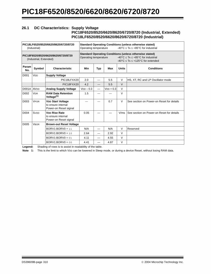
PIC18F6520/8520/6620/8620/6720/8720
26.1 DC Characteristics: Supply VoltagePIC18F6520/8520/6620/8620/6720/8720 (Industrial, Extended) PIC18LF6520/8520/6620/8620/6720/8720 (Industrial)
PIC18LF6520/8520/6620/8620/6720/8720 (Industrial)
Standard Operating Conditions (unless otherwise stated)Operating temperature -40°C ≤ TA ≤ +85°C for industrial
PIC18F6520/8520/6620/8620/6720/8720 (Industrial, Extended)
Standard Operating Conditions (unless otherwise stated)Operating temperature -40°C ≤ TA ≤ +85°C for industrial
-40°C ≤ TA ≤ +125°C for extended
Param No.
Symbol Characteristic Min Typ Max Units Conditions
D001 VDD Supply Voltage
PIC18LFXX20 2.0 — 5.5 V HS, XT, RC and LP Oscillator mode
PIC18FXX20 4.2 — 5.5 V
D001A AVDD Analog Supply Voltage VDD – 0.3 — VDD + 0.3 V
D002 VDR RAM Data RetentionVoltage(1)
1.5 — — V
D003 VPOR VDD Start Voltage to ensure internal Power-on Reset signal
— — 0.7 V See section on Power-on Reset for details
D004 SVDD VDD Rise Rateto ensure internal Power-on Reset signal
0.05 — — V/ms See section on Power-on Reset for details
D005 VBOR Brown-out Reset Voltage
BORV1:BORV0 = 11 N/A — N/A V Reserved
BORV1:BORV0 = 10 2.64 — 2.92 V
BORV1:BORV0 = 01 4.11 — 4.55 V
BORV1:BORV0 = 00 4.41 — 4.87 V
Legend: Shading of rows is to assist in readability of the table.Note 1: This is the limit to which VDD can be lowered in Sleep mode, or during a device Reset, without losing RAM data.
DS39609B-page 310 2004 Microchip Technology Inc.
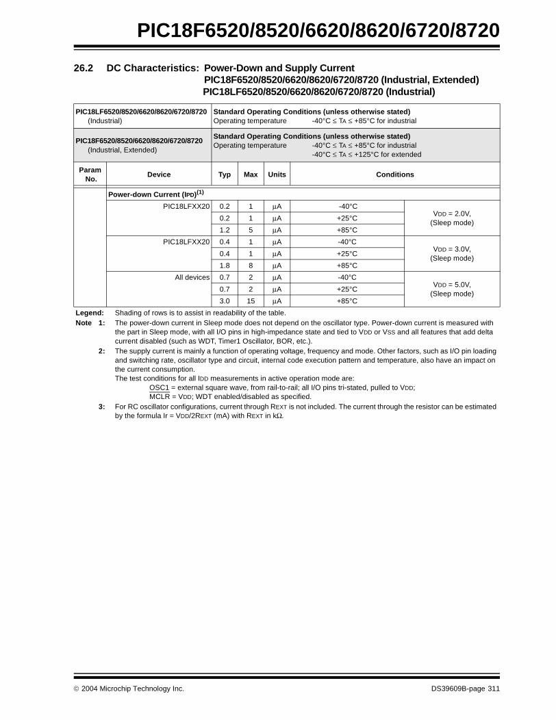
PIC18F6520/8520/6620/8620/6720/8720
26.2 DC Characteristics: Power-Down and Supply CurrentPIC18F6520/8520/6620/8620/6720/8720 (Industrial, Extended) PIC18LF6520/8520/6620/8620/6720/8720 (Industrial)
PIC18LF6520/8520/6620/8620/6720/8720 (Industrial)
Standard Operating Conditions (unless otherwise stated)Operating temperature -40°C ≤ TA ≤ +85°C for industrial
PIC18F6520/8520/6620/8620/6720/8720 (Industrial, Extended)
Standard Operating Conditions (unless otherwise stated)Operating temperature -40°C ≤ TA ≤ +85°C for industrial
-40°C ≤ TA ≤ +125°C for extended
Param No.
Device Typ Max Units Conditions
Power-down Current (IPD)(1)
PIC18LFXX20 0.2 1 µA -40°CVDD = 2.0V,
(Sleep mode)0.2 1 µA +25°C
1.2 5 µA +85°C
PIC18LFXX20 0.4 1 µA -40°CVDD = 3.0V,
(Sleep mode)0.4 1 µA +25°C
1.8 8 µA +85°C
All devices 0.7 2 µA -40°CVDD = 5.0V,
(Sleep mode)0.7 2 µA +25°C
3.0 15 µA +85°C
Legend: Shading of rows is to assist in readability of the table.Note 1: The power-down current in Sleep mode does not depend on the oscillator type. Power-down current is measured with
the part in Sleep mode, with all I/O pins in high-impedance state and tied to VDD or VSS and all features that add delta current disabled (such as WDT, Timer1 Oscillator, BOR, etc.).
2: The supply current is mainly a function of operating voltage, frequency and mode. Other factors, such as I/O pin loading and switching rate, oscillator type and circuit, internal code execution pattern and temperature, also have an impact on the current consumption.The test conditions for all IDD measurements in active operation mode are:
OSC1 = external square wave, from rail-to-rail; all I/O pins tri-stated, pulled to VDD;MCLR = VDD; WDT enabled/disabled as specified.
3: For RC oscillator configurations, current through REXT is not included. The current through the resistor can be estimated by the formula Ir = VDD/2REXT (mA) with REXT in kΩ.
2004 Microchip Technology Inc. DS39609B-page 311

PIC18F6520/8520/6620/8620/6720/8720
Supply Current (IDD)(2,3)
PIC18LFXX20 165 350 µA -40°C
VDD = 2.0V
FOSC = 1 MHZ,EC oscillator
165 350 µA +25°C
170 350 µA +85°C
PIC18LFXX20 360 750 µA -40°C
VDD = 3.0V340 750 µA +25°C
300 750 µA +85°C
All devices 800 1700 µA -40°C
VDD = 5.0V730 1700 µA +25°C
700 1700 µA +85°C
PIC18LFXX20 600 1200 µA -40°C
VDD = 2.0V
FOSC = 4 MHz,EC oscillator
600 1200 µA +25°C
640 1300 µA +85°C
PIC18LFXX20 1000 2500 µA -40°C
VDD = 3.0V1000 2500 µA +25°C
1000 2500 µA +85°C
All devices 2.2 5.0 mA -40°C
VDD = 5.0V2.1 5.0 mA +25°C
2.0 5.0 mA +85°C
26.2 DC Characteristics: Power-Down and Supply CurrentPIC18F6520/8520/6620/8620/6720/8720 (Industrial, Extended) PIC18LF6520/8520/6620/8620/6720/8720 (Industrial) (Continued)
PIC18LF6520/8520/6620/8620/6720/8720 (Industrial)
Standard Operating Conditions (unless otherwise stated)Operating temperature -40°C ≤ TA ≤ +85°C for industrial
PIC18F6520/8520/6620/8620/6720/8720 (Industrial, Extended)
Standard Operating Conditions (unless otherwise stated)Operating temperature -40°C ≤ TA ≤ +85°C for industrial
-40°C ≤ TA ≤ +125°C for extended
Param No.
Device Typ Max Units Conditions
Legend: Shading of rows is to assist in readability of the table.Note 1: The power-down current in Sleep mode does not depend on the oscillator type. Power-down current is measured with
the part in Sleep mode, with all I/O pins in high-impedance state and tied to VDD or VSS and all features that add delta current disabled (such as WDT, Timer1 Oscillator, BOR, etc.).
2: The supply current is mainly a function of operating voltage, frequency and mode. Other factors, such as I/O pin loading and switching rate, oscillator type and circuit, internal code execution pattern and temperature, also have an impact on the current consumption.The test conditions for all IDD measurements in active operation mode are:
OSC1 = external square wave, from rail-to-rail; all I/O pins tri-stated, pulled to VDD;MCLR = VDD; WDT enabled/disabled as specified.
3: For RC oscillator configurations, current through REXT is not included. The current through the resistor can be estimated by the formula Ir = VDD/2REXT (mA) with REXT in kΩ.
DS39609B-page 312 2004 Microchip Technology Inc.
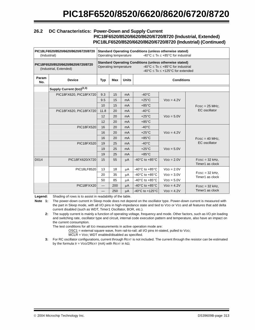
PIC18F6520/8520/6620/8620/6720/8720
Supply Current (IDD)(2,3)
PIC18FX620, PIC18FX720 9.3 15 mA -40°C
VDD = 4.2V
FOSC = 25 MHZ,EC oscillator
9.5 15 mA +25°C
10 15 mA +85°C
PIC18FX620, PIC18FX720 11.8 20 mA -40°C
VDD = 5.0V12 20 mA +25°C
12 20 mA +85°C
PIC18FX520 16 20 mA -40°C
VDD = 4.2V
FOSC = 40 MHZ,EC oscillator
16 20 mA +25°C
16 20 mA +85°C
PIC18FX520 19 25 mA -40°C
VDD = 5.0V19 25 mA +25°C
19 25 mA +85°C
D014 PIC18FX620/X720 15 55 µA -40°C to +85°C VDD = 2.0V FOSC = 32 kHz, Timer1 as clock
PIC18LF8520 13 18 µA -40°C to +85°C VDD = 2.0VFOSC = 32 kHz, Timer1 as clock
20 35 µA -40°C to +85°C VDD = 3.0V
50 85 µA -40°C to +85°C VDD = 5.0V
PIC18FXX20 — 200 µA -40°C to +85°C VDD = 4.2V FOSC = 32 kHz, Timer1 as clock— 250 µA -40°C to +125°C VDD = 4.2V
26.2 DC Characteristics: Power-Down and Supply CurrentPIC18F6520/8520/6620/8620/6720/8720 (Industrial, Extended) PIC18LF6520/8520/6620/8620/6720/8720 (Industrial) (Continued)
PIC18LF6520/8520/6620/8620/6720/8720 (Industrial)
Standard Operating Conditions (unless otherwise stated)Operating temperature -40°C ≤ TA ≤ +85°C for industrial
PIC18F6520/8520/6620/8620/6720/8720 (Industrial, Extended)
Standard Operating Conditions (unless otherwise stated)Operating temperature -40°C ≤ TA ≤ +85°C for industrial
-40°C ≤ TA ≤ +125°C for extended
Param No.
Device Typ Max Units Conditions
Legend: Shading of rows is to assist in readability of the table.Note 1: The power-down current in Sleep mode does not depend on the oscillator type. Power-down current is measured with
the part in Sleep mode, with all I/O pins in high-impedance state and tied to VDD or VSS and all features that add delta current disabled (such as WDT, Timer1 Oscillator, BOR, etc.).
2: The supply current is mainly a function of operating voltage, frequency and mode. Other factors, such as I/O pin loading and switching rate, oscillator type and circuit, internal code execution pattern and temperature, also have an impact on the current consumption.The test conditions for all IDD measurements in active operation mode are:
OSC1 = external square wave, from rail-to-rail; all I/O pins tri-stated, pulled to VDD;MCLR = VDD; WDT enabled/disabled as specified.
3: For RC oscillator configurations, current through REXT is not included. The current through the resistor can be estimated by the formula Ir = VDD/2REXT (mA) with REXT in kΩ.
2004 Microchip Technology Inc. DS39609B-page 313

PIC18F6520/8520/6620/8620/6720/8720
Module Differential Currents (∆IWDT, ∆IBOR, ∆ILVD, ∆IOSCB, ∆IAD)
D022(∆IWDT)
Watchdog Timer <1 2.0 µA -40°C
VDD = 2.0V<1 1.5 µA +25°C
<1 3 µA +85°C
3 10 µA -40°C
VDD = 3.0V2.5 6 µA +25°C
3 15 µA +85°C
15 25 µA -40°C
VDD = 5.0V12 20 µA +25°C
12 40 µA +85°C
D022A(∆IBOR)
Brown-out Reset 35 50 µA -40°C to +85°C VDD = 3.0V
45 65 µA -40°C to +85°C VDD = 5.0V
D022B(∆ILVD)
Low-Voltage Detect 33 45 µA -40°C to +85°C VDD = 2.0V
35 50 µA -40°C to +85°C VDD = 3.0V
45 65 µA -40°C to +85°C VDD = 5.0V
D025(∆IOSCB)
Timer1 Oscillator 5.2 30 µA +25°C VDD = 2.0V
32 kHz on Timer1PIC18LF8720/8620 5.2 40 µA -40°C to +85°C VDD = 2.0V
6.5 50 µA -40°C to +125°C VDD = 4.2V
PIC18F8520/8620/8720 6.5 40 µA +25°C
VDD = 4.2V 32 kHz on Timer16.5 50 µA -40°C to +85°C
6.5 65 µA -40°C to +125°C
PIC18LF8520 1.8 2.2 µA +25°C VDD = 2.0V
32 kHz on Timer12.9 3.8 µA -40°C to +85°C VDD = 3.0V
3.4 7.0 µA -40°C to +125°C VDD = 5.0V
D026(∆IAD)
A/D Converter <1 2 µA +25°C VDD = 2.0VA/D on, not converting.
Device is in Sleep.<1 2 µA +25°C VDD = 3.0V
<1 2 µA +25°C VDD = 5.0V
26.2 DC Characteristics: Power-Down and Supply CurrentPIC18F6520/8520/6620/8620/6720/8720 (Industrial, Extended) PIC18LF6520/8520/6620/8620/6720/8720 (Industrial) (Continued)
PIC18LF6520/8520/6620/8620/6720/8720 (Industrial)
Standard Operating Conditions (unless otherwise stated)Operating temperature -40°C ≤ TA ≤ +85°C for industrial
PIC18F6520/8520/6620/8620/6720/8720 (Industrial, Extended)
Standard Operating Conditions (unless otherwise stated)Operating temperature -40°C ≤ TA ≤ +85°C for industrial
-40°C ≤ TA ≤ +125°C for extended
Param No.
Device Typ Max Units Conditions
Legend: Shading of rows is to assist in readability of the table.Note 1: The power-down current in Sleep mode does not depend on the oscillator type. Power-down current is measured with
the part in Sleep mode, with all I/O pins in high-impedance state and tied to VDD or VSS and all features that add delta current disabled (such as WDT, Timer1 Oscillator, BOR, etc.).
2: The supply current is mainly a function of operating voltage, frequency and mode. Other factors, such as I/O pin loading and switching rate, oscillator type and circuit, internal code execution pattern and temperature, also have an impact on the current consumption.The test conditions for all IDD measurements in active operation mode are:
OSC1 = external square wave, from rail-to-rail; all I/O pins tri-stated, pulled to VDD;MCLR = VDD; WDT enabled/disabled as specified.
3: For RC oscillator configurations, current through REXT is not included. The current through the resistor can be estimated by the formula Ir = VDD/2REXT (mA) with REXT in kΩ.
DS39609B-page 314 2004 Microchip Technology Inc.

PIC18F6520/8520/6620/8620/6720/8720
26.3 DC Characteristics: PIC18F6520/8520/6620/8620/6720/8720 (Industrial, Extended) PIC18LF6520/8520/6620/8620/6720/8720 (Industrial)
DC CHARACTERISTICSStandard Operating Conditions (unless otherwise stated)Operating temperature -40°C ≤ TA ≤ +85°C for industrial
-40°C ≤ TA ≤ +125°C for extended
ParamNo.
Sym Characteristic Min Max Units Conditions
VIL Input Low Voltage
I/O ports:
D030 with TTL buffer VSS 0.15 VDD V VDD < 4.5V
D030A — 0.8 V 4.5V ≤ VDD ≤ 5.5V
D031 with Schmitt Trigger bufferRC3 and RC4
VSS
VSS
0.2 VDD
0.3 VDD
VV
D032 MCLR VSS 0.2 VDD V
D032A OSC1 (in XT, HS and LP modes) and T1OSI
VSS 0.2 VDD V
D033 OSC1 (in RC and EC mode)(1) VSS 0.2 VDD V
VIH Input High Voltage
I/O ports:
D040 with TTL buffer 0.25 VDD + 0.8V VDD V VDD < 4.5V
D040A 2.0 VDD V 4.5V ≤ VDD ≤ 5.5V
D041 with Schmitt Trigger bufferRC3 and RC4
0.8 VDD
0.7 VDD
VDD
VDD
VV
D042 MCLR, OSC1 (EC mode) 0.8 VDD VDD V
D042A OSC1 and T1OSI 1.6 VDD V LP, XT, HS, HSPLL modes(1)
D043 OSC1 (RC mode)(1) 0.9 VDD VDD V
IIL Input Leakage Current(2,3)
D060 I/O ports — ±1 µA VSS ≤ VPIN ≤ VDD, Pin at high-impedance
D061 MCLR — ±5 µA VSS ≤ VPIN ≤ VDD
D063 OSC1 — ±5 µA VSS ≤ VPIN ≤ VDD
IPU Weak Pull-up Current
D070 IPURB PORTB weak pull-up current 50 400 µA VDD = 5V, VPIN = VSS
Note 1: In RC oscillator configuration, the OSC1/CLKI pin is a Schmitt Trigger input. It is not recommended that the PICmicro device be driven with an external clock while in RC mode.
2: The leakage current on the MCLR pin is strongly dependent on the applied voltage level. The specified levels represent normal operating conditions. Higher leakage current may be measured at different input voltages.
3: Negative current is defined as current sourced by the pin.
4: Parameter is characterized but not tested.
2004 Microchip Technology Inc. DS39609B-page 315

PIC18F6520/8520/6620/8620/6720/8720
VOL Output Low Voltage
D080 I/O ports — 0.6 V IOL = 8.5 mA, VDD = 4.5V, -40°C to +85°C
D080A — 0.6 V IOL = 7.0 mA, VDD = 4.5V, -40°C to +125°C
D083 OSC2/CLKO (RC mode)
— 0.6 V IOL = 1.6 mA, VDD = 4.5V, -40°C to +85°C
D083A — 0.6 V IOL = 1.2 mA, VDD = 4.5V, -40°C to +125°C
VOH Output High Voltage(3)
D090 I/O ports VDD – 0.7 — V IOH = -3.0 mA, VDD = 4.5V, -40°C to +85°C
D090A VDD – 0.7 — V IOH = -2.5 mA, VDD = 4.5V, -40°C to +125°C
D092 OSC2/CLKO (RC mode)
VDD – 0.7 — V IOH = -1.3 mA, VDD = 4.5V, -40°C to +85°C
D092A VDD – 0.7 — V IOH = -1.0 mA, VDD = 4.5V, -40°C to +125°C
D150 VOD Open-Drain High Voltage — 8.5 V RA4 pin
Capacitive Loading Specson Output Pins
D100(4) COSC2 OSC2 pin — 15 pF In XT, HS and LP modes when external clock is used to drive OSC1
D101 CIO All I/O pins and OSC2 (in RC mode)
— 50 pF To meet the AC Timing Specifications
D102 CB SCL, SDA — 400 pF In I2C mode
26.3 DC Characteristics: PIC18F6520/8520/6620/8620/6720/8720 (Industrial, Extended) PIC18LF6520/8520/6620/8620/6720/8720 (Industrial) (Continued)
DC CHARACTERISTICSStandard Operating Conditions (unless otherwise stated)Operating temperature -40°C ≤ TA ≤ +85°C for industrial
-40°C ≤ TA ≤ +125°C for extended
ParamNo.
Sym Characteristic Min Max Units Conditions
Note 1: In RC oscillator configuration, the OSC1/CLKI pin is a Schmitt Trigger input. It is not recommended that the PICmicro device be driven with an external clock while in RC mode.
2: The leakage current on the MCLR pin is strongly dependent on the applied voltage level. The specified levels represent normal operating conditions. Higher leakage current may be measured at different input voltages.
3: Negative current is defined as current sourced by the pin.
4: Parameter is characterized but not tested.
DS39609B-page 316 2004 Microchip Technology Inc.

PIC18F6520/8520/6620/8620/6720/8720
TABLE 26-1: COMPARATOR SPECIFICATIONS
TABLE 26-2: VOLTAGE REFERENCE SPECIFICATIONS
Operating Conditions: 3.0V < VDD < 5.5V, -40°C < TA < +125°C (unless otherwise stated).
ParamNo.
Sym Characteristics Min Typ Max Units Comments
D300 VIOFF Input Offset Voltage — ± 5.0 ± 10 mV
D301 VICM Input Common Mode Voltage 0 — VDD – 1.5 V
D302 CMRR Common Mode Rejection Ratio 55 — — dB
300300A
TRESP Response Time(1) — 150 400600
nsns
PIC18FXX20PIC18LFXX20
301 TMC2OV Comparator Mode Change to Output Valid
— — 10 µs
Note 1: Response time measured with one comparator input at (VDD – 1.5)/2, while the other input transitions from VSS to VDD.
Operating Conditions: 3.0V < VDD < 5.5V, -40°C < TA < +125°C (unless otherwise stated).
ParamNo.
Sym Characteristics Min Typ Max Units Comments
D310 VRES Resolution VDD/24 — VDD/32 LSb
D311 VRAA Absolute Accuracy ——
——
1/41/2
LSbLSb
Low Range (VRR = 1)High Range (VRR = 0)
D312 VRUR Unit Resistor Value (R) — 2k — Ω310 TSET Settling Time(1) — — 10 µs
Note 1: Settling time measured while VRR = 1 and VR<3:0> transitions from ‘0000’ to ‘1111’.
2004 Microchip Technology Inc. DS39609B-page 317

PIC18F6520/8520/6620/8620/6720/8720
FIGURE 26-5: LOW-VOLTAGE DETECT CHARACTERISTICS
TABLE 26-3: LOW-VOLTAGE DETECT CHARACTERISTICS
VLVD
LVDIF
VDD
(LVDIF set by hardware)
(LVDIF can be cleared in software)
Standard Operating Conditions (unless otherwise stated)Operating temperature -40°C ≤ TA ≤ +85°C for industrial
-40°C ≤ TA ≤ +125°C for extended
Param No.
Symbol Characteristic Min Typ† Max Units Conditions
D420 LVD Voltage on VDD Transition high-to-low
LVV = 0001 1.96 2.06 2.16 V
LVV = 0010 2.16 2.27 2.38 V
LVV = 0011 2.35 2.47 2.59 V
LVV = 0100 2.45 2.58 2.71 V
LVV = 0101 2.64 2.78 2.92 V
LVV = 0110 2.75 2.89 3.03 V
LVV = 0111 2.95 3.1 3.26 V
LVV = 1000 3.24 3.41 3.58 V
LVV = 1001 3.43 3.61 3.79 V
LVV = 1010 3.53 3.72 3.91 V
LVV = 1011 3.72 3.92 4.12 V
LVV = 1100 3.92 4.13 4.34 V
LVV = 1101 4.11 4.33 4.55 V
LVV = 1110 4.41 4.64 4.87 V
D423 VBG Band Gap Reference Voltage Value — 1.22 — V
† Production tested at TAMB = 25°C. Specifications over temperature limits ensured by characterization.
DS39609B-page 318 2004 Microchip Technology Inc.

PIC18F6520/8520/6620/8620/6720/8720
TABLE 26-4: MEMORY PROGRAMMING REQUIREMENTS
DC CharacteristicsStandard Operating Conditions (unless otherwise stated)Operating temperature -40°C ≤ TA ≤ +85°C for industrial
-40°C ≤ TA ≤ +125°C for extended
ParamNo.
Sym Characteristic Min Typ† Max Units Conditions
Internal Program Memory Programming Specifications(Note 1)
D110 VPP Voltage on MCLR/VPP pin 9.00 — 13.25 V (Note 2)
D112 IPP Current into MCLR/VPP pin — — 5 µA
D113 IDDP Supply Current during Programming
— — 10 mA
Data EEPROM Memory
D120 ED Cell Endurance 100K 1M — E/W -40°C to +85°CD120A ED Cell Endurance 10K 100K — E/W +85°C to +125°CD121 VDRW VDD for Read/Write VMIN — 5.5 V Using EECON to read/write
VMIN = Minimum operating voltage
D122 TDEW Erase/Write Cycle Time — 4 — ms
D123 TRETD Characteristic Retention 40 — — Year -40°C to +85°C (Note 3)
D123A TRETD Characteristic Retention 100 — — Year 25°C (Note 3)
Program Flash Memory
D130 EP Cell Endurance 10K 100K — E/W -40°C to +85°CD130A EP Cell Endurance 1000 10K — E/W +85°C to +125°CD131 VPR VDD for Read VMIN — 5.5 V VMIN = Minimum operating
voltage
D132 VIE VDD for Block Erase 4.5 — 5.5 V Using ICSP port
D132A VIW VDD for Externally Timed Erase or Write
4.5 — 5.5 V Using ICSP port
D132B VPEW VDD for Self-Timed Write VMIN — 5.5 V VMIN = Minimum operating voltage
D133 TIE ICSP Block Erase Cycle Time — 5 — ms VDD > 4.5V
D133A TIW ICSP Erase or Write Cycle Time (externally timed)
1 — — ms VDD > 4.5V
D133A TIW Self-Timed Write Cycle Time — 2.5 — ms
D134 TRETD Characteristic Retention 40 — — Year -40°C to +85°C (Note 3)
D134A TRETD Characteristic Retention 100 — — Year 25°C (Note 3)
† Data in “Typ” column is at 5.0V, 25°C unless otherwise stated. These parameters are for design guidance only and are not tested.
Note 1: These specifications are for programming the on-chip program memory through the use of table write instructions.
2: The pin may be kept in this range at times other than programming, but it is not recommended.
3: Retention time is valid, provided no other specifications are violated.
2004 Microchip Technology Inc. DS39609B-page 319

PIC18F6520/8520/6620/8620/6720/8720
26.4 AC (Timing) Characteristics
26.4.1 TIMING PARAMETER SYMBOLOGY
The timing parameter symbols have been createdusing one of the following formats:
1. TppS2ppS 3. TCC:ST (I2C specifications only)2. TppS 4. Ts (I2C specifications only)T
F Frequency T TimeLowercase letters (pp) and their meanings:pp
cc CCP1 osc OSC1ck CLKO rd RDcs CS rw RD or WR
di SDI sc SCKdo SDO ss SSdt Data in t0 T0CKI
io I/O port t1 T1CKImc MCLR wr WR
Uppercase letters and their meanings:
SF Fall P PeriodH High R Rise
I Invalid (High-Impedance) V ValidL Low Z High-Impedance
I2C only
AA output access High HighBUF Bus free Low Low
TCC:ST (I2C specifications only)
CCHD Hold SU Setup
ST
DAT DATA input hold STO Stop conditionSTA Start condition
DS39609B-page 320 2004 Microchip Technology Inc.

PIC18F6520/8520/6620/8620/6720/8720
26.4.2 TIMING CONDITIONS
The temperature and voltages specified in Table 26-5apply to all timing specifications unless otherwisenoted. Figure 26-6 specifies the load conditions for thetiming specifications.
TABLE 26-5: TEMPERATURE AND VOLTAGE SPECIFICATIONS – AC
FIGURE 26-6: LOAD CONDITIONS FOR DEVICE TIMING SPECIFICATIONS
AC CHARACTERISTICS
Standard Operating Conditions (unless otherwise stated)Operating temperature -40°C ≤ TA ≤ +85°C for industrial
-40°C ≤ TA ≤ +125°C for extendedOperating voltage VDD range as described in DC spec Section 26.1 and Section 26.3. LC parts operate for industrial temperatures only.
VDD/2
CL
RL
Pin
Pin
VSS
VSS
CL
RL = 464Ω
CL = 50 pF for all pins except OSC2/CLKOand including D and E outputs as ports
Load condition 1 Load condition 2
2004 Microchip Technology Inc. DS39609B-page 321

PIC18F6520/8520/6620/8620/6720/8720
26.4.3 TIMING DIAGRAMS AND SPECIFICATIONS
FIGURE 26-7: EXTERNAL CLOCK TIMING (ALL MODES EXCEPT PLL)
TABLE 26-6: EXTERNAL CLOCK TIMING REQUIREMENTS Param
No.Symbol Characteristic Min Max Units Conditions
1A FOSC External CLKI Frequency(1) DC 25 MHz EC, ECIO, PIC18FX620/X720(-40°C to +85°C)
DC 40 MHz EC, ECIO, PIC18FX520 (-40°C to +85°C)
DC 25 MHz EC, ECIO, PIC18FX520 using external memory interface (-40°C to +85°C)
Oscillator Frequency(1) DC 4 MHz RC oscillator
0.1 4 MHz XT oscillator
4 25 MHz HS oscillator
4 10 MHz HS + PLL oscillator, PIC18FX520
4 6.25 MHz HS + PLL oscillator, PIC18FX520 using external memory interface
4 6.25 MHz HS + PLL oscillator, PIC18FX620/X720
5 33 kHz LP Oscillator mode
1 TOSC External CLKI Period(1) 40 — ns EC, ECIO, PIC18FX620/X720(-40°C to +85°C)
25
40
—
—
ns
ns
EC, ECIO, PIC18FX520 (-40°C to +85°C)
EC, ECIO, PIC18FX520 using external memory interface (-40°C to +85°C)
Oscillator Period(1) 250 — ns RC oscillator
250 10,000 ns XT oscillator
40
100
160
250
250
250
ns
ns
ns
HS oscillator
HS + PLL oscillator, PIC18FX520
HS + PLL oscillator, PIC18FX620/X720
30 200 µs LP oscillator
2 TCY Instruction Cycle Time(1) 100 — ns TCY = 4/FOSC
3 TOSL,TOSH
External Clock in (OSC1) High or Low Time
30 — ns XT oscillator
2.5 — µs LP oscillator
10 — ns HS oscillator
4 TOSR,TOSF
External Clock in (OSC1) Rise or Fall Time
— 20 ns XT oscillator
— 50 ns LP oscillator
— 7.5 ns HS oscillator
Note 1: Instruction cycle period (TCY) equals four times the input oscillator time base period for all configurations except PLL. All specified values are based on characterization data for that particular oscillator type under standard operating conditions with the device executing code. Exceeding these specified limits may result in an unstable oscillator operation and/or higher than expected current consumption. All devices are tested to operate at “min.” values with an external clock applied to the OSC1/CLKI pin. When an external clock input is used, the “max.” cycle time limit is “DC” (no clock) for all devices.
OSC1
CLKO
Q4 Q1 Q2 Q3 Q4 Q1
1
2
3 3 4 4
DS39609B-page 322 2004 Microchip Technology Inc.
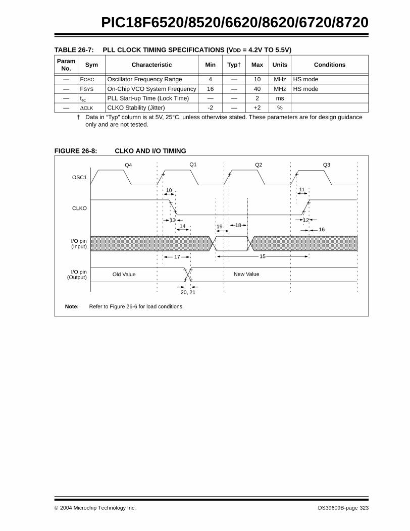
PIC18F6520/8520/6620/8620/6720/8720
TABLE 26-7: PLL CLOCK TIMING SPECIFICATIONS (VDD = 4.2V TO 5.5V)
FIGURE 26-8: CLKO AND I/O TIMING
Param No.
Sym Characteristic Min Typ† Max Units Conditions
— FOSC Oscillator Frequency Range 4 — 10 MHz HS mode
— FSYS On-Chip VCO System Frequency 16 — 40 MHz HS mode
— trc PLL Start-up Time (Lock Time) — — 2 ms
— ∆CLK CLKO Stability (Jitter) -2 — +2 %
† Data in “Typ” column is at 5V, 25°C, unless otherwise stated. These parameters are for design guidance only and are not tested.
Note: Refer to Figure 26-6 for load conditions.
OSC1
CLKO
I/O pin(Input)
I/O pin(Output)
Q4 Q1 Q2 Q3
10
1314
17
20, 21
19 18
15
11
12
16
Old Value New Value
2004 Microchip Technology Inc. DS39609B-page 323

PIC18F6520/8520/6620/8620/6720/8720
TABLE 26-8: CLKO AND I/O TIMING REQUIREMENTS
FIGURE 26-9: PROGRAM MEMORY READ TIMING DIAGRAM
Param No.
Symbol Characteristic Min Typ Max Units Conditions
10 TOSH2CKL OSC1 ↑ to CLKO ↓ — 75 200 ns (Note 1)
11 TOSH2CKH OSC1 ↑ to CLKO ↑ — 75 200 ns (Note 1)
12 TCKR CLKO Rise Time — 35 100 ns (Note 1)
13 TCKF CLKO Fall Time — 35 100 ns (Note 1)
14 TCKL2IOV CLKO ↓ to Port Out Valid — — 0.5 TCY + 20 ns (Note 1)
15 TIOV2CKH Port In Valid before CLKO ↑ 0.25 TCY + 25 — — ns (Note 1)
16 TCKH2IOI Port In Hold after CLKO ↑ 0 — — ns (Note 1)
17 TOSH2IOV OSC1 ↑ (Q1 cycle) to Port Out Valid — 50 150 ns
18 TOSH2IOI OSC1 ↑ (Q2 cycle) to Port Input Invalid (I/O in hold time)
PIC18FXX20 100 — — ns
18A PIC18LFXX20 200 — — ns VDD = 2.0V
19 TIOV2OSH Port Input Valid to OSC1 ↑ (I/O in setup time) 0 — — ns
20 TIOR Port Output Rise Time PIC18FXX20 — 10 25 ns
20A PIC18LFXX20 — — 60 ns VDD = 2.0V
21 TIOF Port Output Fall Time PIC18FXX20 — 10 25 ns
21A PIC18LFXX20 — — 60 ns VDD = 2.0V
22† TINP INT pin High or Low Time TCY — — ns
23† TRBP RB7:RB4 Change INT High or Low Time TCY — — ns
24† TRCP RC7:RC4 Change INT High or Low Time 20 — — ns
† These parameters are asynchronous events not related to any internal clock edges.Note 1: Measurements are taken in RC mode, where CLKO output is 4 x TOSC.
Q1 Q2 Q3 Q4 Q1 Q2
OSC1(1)
ALE
OE
Address Data from External
166
160
165
161151 162
163
AD<15:0>
167168
155
Address
Address
150
A<19:16> Address
169
BA0
CE171
171A
164
Operating Conditions: 2.0V < VCC < 5.5V, -40°C < TA < +125°C unless otherwise stated.Note 1: Maximum speed of FOSC is 25 MHz for external program memory read.
DS39609B-page 324 2004 Microchip Technology Inc.

PIC18F6520/8520/6620/8620/6720/8720
TABLE 26-9: CLKO AND I/O TIMING REQUIREMENTS
FIGURE 26-10: PROGRAM MEMORY WRITE TIMING DIAGRAM
Param No.
Symbol Characteristics Min Typ Max Units
150 TADV2ALL Address Out Valid to ALE ↓ (address setup time)
0.25 TCY – 10 — — ns
151 TALL2ADL ALE ↓ to Address Out Invalid (address hold time) 5 — — ns
155 TALL2OEL ALE ↓ to OE ↓ 10 0.125 TCY — ns
160 TADZ2OEL AD high-Z to OE ↓ (bus release to OE) 0 — — ns
161 TOEH2ADD OE ↑ to AD Driven 0.125 TCY – 5 — — ns
162 TADV2OEH LS Data Valid before OE ↑ (data setup time) 20 — — ns
163 TOEH2ADL OE ↑ to Data In Invalid (data hold time) 0 — — ns
164 TALH2ALL ALE Pulse Width — 0.25 TCY — ns
165 TOEL2OEH OE Pulse Width 0.5 TCY – 5 0.5 TCY — ns
166 TALH2ALH ALE ↑ to ALE ↑ (cycle time) — TCY — ns
167 TACC Address Valid to Data Valid 0.75 TCY – 25 — — ns
168 TOE OE ↓ to Data Valid — 0.5 TCY – 25 ns
169 TALL2OEH ALE ↓ to OE ↑ 0.625 TCY – 10 — 0.625 TCY + 10 ns
171 TALH2CSL Chip Enable Active to ALE ↓ — — 10 ns
171A TUBL2OEH AD Valid to Chip Enable Active 0.25 TCY – 20 — — ns
Q1 Q2 Q3 Q4 Q1 Q2
OSC1(1)
ALE
Address Data
156150
151
153
AD<15:0> Address
WRH orWRL
UB orLB
157
154
157A
AddressA<19:16> Address
BA0
166
CE
171
171A
Operating Conditions: 2.0V < VCC < 5.5V, -40°C < TA < +125°C unless otherwise stated.Note 1: Maximum speed of FOSC is 25 MHz for external program memory read.
2004 Microchip Technology Inc. DS39609B-page 325

PIC18F6520/8520/6620/8620/6720/8720
TABLE 26-10: PROGRAM MEMORY WRITE TIMING REQUIREMENTS
FIGURE 26-11: RESET, WATCHDOG TIMER, OSCILLATOR START-UP TIMER AND POWER-UP TIMER TIMING
Param No.
Symbol Characteristics Min Typ Max Units
150 TADV2ALL Address Out Valid to ALE ↓ (address setup time) 0.25 TCY – 10 — — ns
151 TALL2ADL ALE ↓ to Address Out Invalid (address hold time) 5 — — ns
153 TWRH2ADL WRn ↑ to Data Out Invalid (data hold time) 5 — — ns
154 TWRL WRn Pulse Width 0.5 TCY – 5 0.5 TCY — ns
156 TADV2WRH Data Valid before WRn ↑ (data setup time) 0.5 TCY – 10 — — ns
157 TBSV2WRL Byte Select Valid before WRn ↓ (byte select setup time)
0.25 TCY — — ns
157A TWRH2BSI WRn ↑ to Byte Select Invalid (byte select hold time) 0.125 TCY – 5 — — ns
166 TALH2ALH ALE ↑ to ALE ↑ (cycle time) — TCY — ns
171 TALH2CSL Chip Enable Active to ALE ↓ — — 10 ns
171A TUBL2OEH AD Valid to Chip Enable Active 0.25 TCY – 20 — — ns
VDD
MCLR
InternalPOR
PWRTTime-out
OSCTime-out
InternalReset
WatchdogTimerReset
33
32
30
3134
I/O Pins
34
Note: Refer to Figure 26-6 for load conditions.
DS39609B-page 326 2004 Microchip Technology Inc.

PIC18F6520/8520/6620/8620/6720/8720
FIGURE 26-12: BROWN-OUT RESET TIMING
TABLE 26-11: RESET, WATCHDOG TIMER, OSCILLATOR START-UP TIMER, POWER-UP TIMER AND BROWN-OUT RESET REQUIREMENTS
FIGURE 26-13: TIMER0 AND TIMER1 EXTERNAL CLOCK TIMINGS
VDDBVDD
35VBGAP = 1.2V
VIRVST
Enable Internal
Internal Reference 36
Reference Voltage
Voltage Stable
ParamNo.
Symbol Characteristic Min Typ Max Units Conditions
30 TMCL MCLR Pulse Width (low) 2 — — µs
31 TWDT Watchdog Timer Time-out Period (no postscaler)
7 18 33 ms
32 TOST Oscillation Start-up Timer Period 1024 TOSC — 1024 TOSC — TOSC = OSC1 period
33 TPWRT Power-up Timer Period 28 72 132 ms
34 TIOZ I/O High-Impedance from MCLR Low or Watchdog Timer Reset
— 2 — µs
35 TBOR Brown-out Reset Pulse Width 200 — — µs VDD ≤ BVDD (see D005)
36 TIVRST Time for Internal Reference Voltage to become stable
— 20 50 µs
37 TLVD Low-Voltage Detect Pulse Width 200 — — µs VDD ≤ VLVD
Note: Refer to Figure 26-6 for load conditions.
46
47
45
48
41
42
40
T0CKI
T1OSO/T13CKI
TMR0 orTMR1
2004 Microchip Technology Inc. DS39609B-page 327

PIC18F6520/8520/6620/8620/6720/8720
TABLE 26-12: TIMER0 AND TIMER1 EXTERNAL CLOCK REQUIREMENTS
FIGURE 26-14: CAPTURE/COMPARE/PWM TIMINGS (ALL CCP MODULES)
ParamNo.
Symbol Characteristic Min Max Units Conditions
40 TT0H T0CKI High Pulse Width No prescaler 0.5 TCY + 20 — ns
With prescaler 10 — ns
41 TT0L T0CKI Low Pulse Width No prescaler 0.5 TCY + 20 — ns
With prescaler 10 — ns
42 TT0P T0CKI Period No prescaler TCY + 10 — ns
With prescaler Greater of:20 ns or TCY + 40
N
— ns N = prescalevalue (1, 2, 4,..., 256)
45 TT1H T13CKI High Time
Synchronous, no prescaler 0.5 TCY + 20 — ns
Synchronous,with prescaler
PIC18FXX20 10 — ns
PIC18LFXX20 25 — ns
Asynchronous PIC18FXX20 30 — ns
PIC18LFXX20 50 — ns
46 TT1L T13CKI Low Time
Synchronous, no prescaler 0.5 TCY + 5 — ns
Synchronous, with prescaler
PIC18FXX20 10 — ns
PIC18LFXX20 25 — ns
Asynchronous PIC18FXX20 30 — ns
PIC18LFXX20 TBD TBD ns
47 TT1P T13CKI Input Period
Synchronous Greater of:20 ns or TCY + 40
N
— ns N = prescalevalue (1, 2, 4, 8)
Asynchronous 60 — ns
FT1 T13CKI Oscillator Input Frequency Range DC 50 kHz
48 TCKE2TMRI Delay from External T13CKI Clock Edge to Timer Increment
2 TOSC 7 TOSC —
Note: Refer to Figure 26-6 for load conditions.
CCPx(Capture Mode)
50 51
52
CCPx
53 54
(Compare or PWM Mode)
DS39609B-page 328 2004 Microchip Technology Inc.

PIC18F6520/8520/6620/8620/6720/8720
TABLE 26-13: CAPTURE/COMPARE/PWM REQUIREMENTS (ALL CCP MODULES)
FIGURE 26-15: PARALLEL SLAVE PORT TIMING (PIC18F8X20)
ParamNo.
Symbol Characteristic Min Max Units Conditions
50 TCCL CCPx Input Low Time
No prescaler 0.5 TCY + 20 — ns
With prescaler
PIC18FXX20 10 — ns
PIC18LFXX20 20 — ns
51 TCCH CCPx Input High Time
No prescaler 0.5 TCY + 20 — ns
Withprescaler
PIC18FXX20 10 — ns
PIC18LFXX20 20 — ns
52 TCCP CCPx Input Period 3 TCY + 40N
— ns N = prescale value (1, 4 or 16)
53 TCCR CCPx Output Rise Time PIC18FXX20 — 25 ns
PIC18LFXX20 — 45 ns VDD = 2.0V
54 TCCF CCPx Output Fall Time PIC18FXX20 — 25 ns
PIC18LFXX20 — 45 ns VDD = 2.0V
Note: Refer to Figure 26-6 for load conditions.
RE2/CS
RE0/RD
RE1/WR
RD7:RD0
62
63
64
65
2004 Microchip Technology Inc. DS39609B-page 329
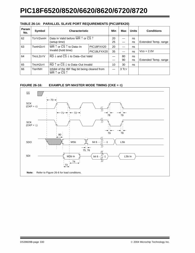
PIC18F6520/8520/6620/8620/6720/8720
TABLE 26-14: PARALLEL SLAVE PORT REQUIREMENTS (PIC18F8X20)
FIGURE 26-16: EXAMPLE SPI MASTER MODE TIMING (CKE = 0)
ParamNo.
Symbol Characteristic Min Max Units Conditions
62 TDTV2WRH Data In Valid before WR ↑ or CS ↑ (setup time)
2025
——
nsns Extended Temp. range
63 TWRH2DTI WR ↑ or CS ↑ to Data–In Invalid (hold time)
PIC18FXX20 20 — ns
PIC18LFXX20 35 — ns VDD = 2.0V
64 TRDL2DTV RD ↓ and CS ↓ to Data–Out Valid ——
8090
nsns Extended Temp. range
65 TRDH2DTI RD ↑ or CS ↓ to Data–Out Invalid 10 30 ns
66 TIBFINH Inhibit of the IBF flag bit being cleared from WR ↑ or CS ↑
— 3 TCY
SS
SCK(CKP = 0)
SCK(CKP = 1)
SDO
SDI
70
71 72
7374
75, 76
787980
7978
MSb LSbbit 6 - - - - - -1
MSb In LSb Inbit 6 - - - -1
Note: Refer to Figure 26-6 for load conditions.
DS39609B-page 330 2004 Microchip Technology Inc.

PIC18F6520/8520/6620/8620/6720/8720
TABLE 26-15: EXAMPLE SPI MODE REQUIREMENTS (MASTER MODE, CKE = 0)
FIGURE 26-17: EXAMPLE SPI MASTER MODE TIMING (CKE = 1)
ParamNo.
Symbol Characteristic Min Max Units Conditions
70 TSSL2SCH, TSSL2SCL
SS ↓ to SCK ↓ or SCK ↑ Input TCY — ns
71 TSCH SCK Input High Time (Slave mode)
Continuous 1.25 TCY + 30 — ns
71A Single Byte 40 — ns (Note 1)
72 TSCL SCK Input Low Time (Slave mode)
Continuous 1.25 TCY + 30 — ns
72A Single Byte 40 — ns (Note 1)
73 TDIV2SCH, TDIV2SCL
Setup Time of SDI Data Input to SCK Edge 100 — ns
73A TB2B Last Clock Edge of Byte 1 to the 1st Clock Edge of Byte 2 1.5 TCY + 40 — ns (Note 2)
74 TSCH2DIL, TSCL2DIL
Hold Time of SDI Data Input to SCK Edge 100 — ns
75 TDOR SDO Data Output Rise Time PIC18FXX20 — 25 ns
PIC18LFXX20 — 45 ns VDD = 2.0V
76 TDOF SDO Data Output Fall Time — 25 ns
78 TSCR SCK Output Rise Time (Master mode)
PIC18FXX20 — 25 ns
PIC18LFXX20 — 45 ns VDD = 2.0V
79 TSCF SCK Output Fall Time (Master mode) — 25 ns
80 TSCH2DOV,TSCL2DOV
SDO Data Output Valid after SCK Edge
PIC18FXX20 — 50 ns
PIC18LFXX20 — 100 ns VDD = 2.0V
Note 1: Requires the use of Parameter #73A.2: Only if Parameter #71A and #72A are used.
SS
SCK(CKP = 0)
SCK(CKP = 1)
SDO
SDI
81
71 72
74
75, 76
78
80
MSb
7973
MSb In
bit 6 - - - - - -1
LSb Inbit 6 - - - -1
LSb
Note: Refer to Figure 26-6 for load conditions.
2004 Microchip Technology Inc. DS39609B-page 331

PIC18F6520/8520/6620/8620/6720/8720
TABLE 26-16: EXAMPLE SPI MODE REQUIREMENTS (MASTER MODE, CKE = 1)
FIGURE 26-18: EXAMPLE SPI SLAVE MODE TIMING (CKE = 0)
Param No.
Symbol Characteristic Min Max Units Conditions
71 TSCH SCK Input High Time (Slave mode)
Continuous 1.25 TCY + 30 — ns
71A Single Byte 40 — ns (Note 1)
72 TSCL SCK Input Low Time (Slave mode)
Continuous 1.25 TCY + 30 — ns
72A Single Byte 40 — ns (Note 1)
73 TDIV2SCH, TDIV2SCL
Setup Time of SDI Data Input to SCK Edge 100 — ns
73A TB2B Last Clock Edge of Byte 1 to the 1st Clock Edge of Byte 2 1.5 TCY + 40 — ns (Note 2)
74 TSCH2DIL, TSCL2DIL
Hold Time of SDI Data Input to SCK Edge 100 — ns
75 TDOR SDO Data Output Rise Time PIC18FXX20 — 25 ns
PIC18LFXX20 — 45 ns VDD = 2.0V
76 TDOF SDO Data Output Fall Time — 25 ns
78 TSCR SCK Output Rise Time (Master mode)
PIC18FXX20 — 25 ns
PIC18LFXX20 — 45 ns VDD = 2.0V
79 TSCF SCK Output Fall Time (Master mode) — 25 ns
80 TSCH2DOV,TSCL2DOV
SDO Data Output Valid after SCK Edge
PIC18FXX20 — 50 ns
PIC18LFXX20 — 100 ns VDD = 2.0V
81 TDOV2SCH,TDOV2SCL
SDO Data Output Setup to SCK Edge TCY — ns
Note 1: Requires the use of Parameter #73A.
2: Only if Parameter #71A and #72A are used.
SS
SCK(CKP = 0)
SCK(CKP = 1)
SDO
SDI
70
71 72
7374
75, 76 77
787980
7978
SDI
MSb LSbbit 6 - - - - - -1
MSb In bit 6 - - - -1 LSb In
83
Note: Refer to Figure 26-6 for load conditions.
DS39609B-page 332 2004 Microchip Technology Inc.
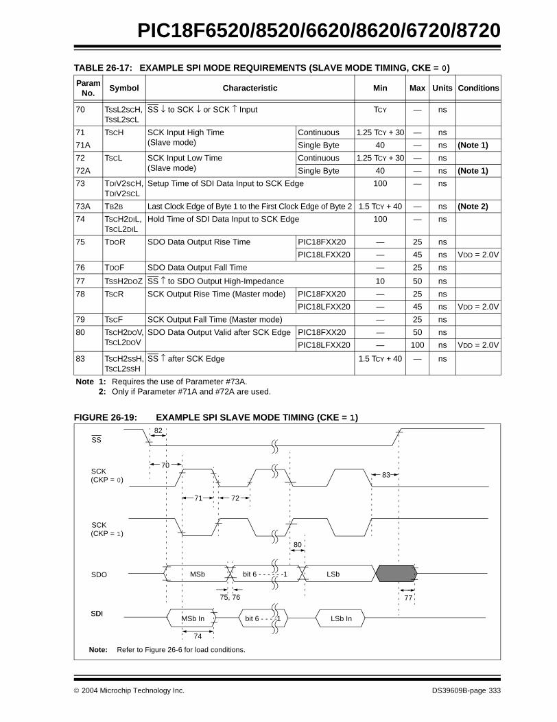
PIC18F6520/8520/6620/8620/6720/8720
TABLE 26-17: EXAMPLE SPI MODE REQUIREMENTS (SLAVE MODE TIMING, CKE = 0)
FIGURE 26-19: EXAMPLE SPI SLAVE MODE TIMING (CKE = 1)
ParamNo.
Symbol Characteristic Min Max Units Conditions
70 TSSL2SCH, TSSL2SCL
SS ↓ to SCK ↓ or SCK ↑ Input TCY — ns
71 TSCH SCK Input High Time (Slave mode)
Continuous 1.25 TCY + 30 — ns
71A Single Byte 40 — ns (Note 1)
72 TSCL SCK Input Low Time (Slave mode)
Continuous 1.25 TCY + 30 — ns
72A Single Byte 40 — ns (Note 1)
73 TDIV2SCH, TDIV2SCL
Setup Time of SDI Data Input to SCK Edge 100 — ns
73A TB2B Last Clock Edge of Byte 1 to the First Clock Edge of Byte 2 1.5 TCY + 40 — ns (Note 2)
74 TSCH2DIL, TSCL2DIL
Hold Time of SDI Data Input to SCK Edge 100 — ns
75 TDOR SDO Data Output Rise Time PIC18FXX20 — 25 ns
PIC18LFXX20 — 45 ns VDD = 2.0V
76 TDOF SDO Data Output Fall Time — 25 ns
77 TSSH2DOZ SS ↑ to SDO Output High-Impedance 10 50 ns
78 TSCR SCK Output Rise Time (Master mode) PIC18FXX20 — 25 ns
PIC18LFXX20 — 45 ns VDD = 2.0V
79 TSCF SCK Output Fall Time (Master mode) — 25 ns
80 TSCH2DOV,TSCL2DOV
SDO Data Output Valid after SCK Edge PIC18FXX20 — 50 ns
PIC18LFXX20 — 100 ns VDD = 2.0V
83 TSCH2SSH,TSCL2SSH
SS ↑ after SCK Edge 1.5 TCY + 40 — ns
Note 1: Requires the use of Parameter #73A.2: Only if Parameter #71A and #72A are used.
SS
SCK(CKP = 0)
SCK(CKP = 1)
SDO
SDI
70
71 72
82
SDI
74
75, 76
MSb bit 6 - - - - - -1 LSb
77
MSb In bit 6 - - - -1 LSb In
80
83
Note: Refer to Figure 26-6 for load conditions.
2004 Microchip Technology Inc. DS39609B-page 333

PIC18F6520/8520/6620/8620/6720/8720
TABLE 26-18: EXAMPLE SPI SLAVE MODE REQUIREMENTS (CKE = 1)
FIGURE 26-20: I2C BUS START/STOP BITS TIMING
ParamNo.
Symbol Characteristic Min Max Units Conditions
70 TSSL2SCH, TSSL2SCL
SS ↓ to SCK ↓ or SCK ↑ Input TCY — ns
71 TSCH SCK Input High Time (Slave mode)
Continuous 1.25 TCY + 30 — ns
71A Single Byte 40 — ns (Note 1)
72 TSCL SCK Input Low Time (Slave mode)
Continuous 1.25 TCY + 30 — ns
72A Single Byte 40 — ns (Note 1)
73A TB2B Last Clock Edge of Byte 1 to the First Clock Edge of Byte 2 1.5 TCY + 40 — ns (Note 2)
74 TSCH2DIL, TSCL2DIL
Hold Time of SDI Data Input to SCK Edge 100 — ns
75 TDOR SDO Data Output Rise Time PIC18FXX20 — 25 ns
PIC18LFXX20 — 45 ns VDD = 2.0V
76 TDOF SDO Data Output Fall Time — 25 ns
77 TSSH2DOZ SS ↑ to SDO Output High-Impedance 10 50 ns
78 TSCR SCK Output Rise Time (Master mode)
PIC18FXX20 — 25 ns
PIC18LFXX20 — 45 ns VDD = 2.0V
79 TSCF SCK Output Fall Time (Master mode) — 25 ns
80 TSCH2DOV,TSCL2DOV
SDO Data Output Valid after SCK Edge
PIC18FXX20 — 50 ns
PIC18LFXX20 — 100 ns VDD = 2.0V
82 TSSL2DOV SDO Data Output Valid after SS ↓ Edge
PIC18FXX20 — 50 ns
PIC18LFXX20 — 100 ns VDD = 2.0V
83 TSCH2SSH,TSCL2SSH
SS ↑ after SCK Edge 1.5 TCY + 40 — ns
Note 1: Requires the use of Parameter #73A.2: Only if Parameter #71A and #72A are used.
Note: Refer to Figure 26-6 for load conditions.
91
92
93SCL
SDA
StartCondition
StopCondition
90
DS39609B-page 334 2004 Microchip Technology Inc.

PIC18F6520/8520/6620/8620/6720/8720
TABLE 26-19: I2C BUS START/STOP BITS REQUIREMENTS (SLAVE MODE)
FIGURE 26-21: I2C BUS DATA TIMING
ParamNo.
Symbol Characteristic Min Max Units Conditions
90 TSU:STA Start Condition 100 kHz mode 4700 — ns Only relevant for Repeated Start conditionSetup Time 400 kHz mode 600 —
91 THD:STA Start Condition 100 kHz mode 4000 — ns After this period, the first clock pulse is generatedHold Time 400 kHz mode 600 —
92 TSU:STO Stop Condition 100 kHz mode 4700 — ns
Setup Time 400 kHz mode 600 —
93 THD:STO Stop Condition 100 kHz mode 4000 — ns
Hold Time 400 kHz mode 600 —
Note: Refer to Figure 26-6 for load conditions.
90
91 92
100
101
103
106 107
109 109110
102
SCL
SDAIn
SDAOut
2004 Microchip Technology Inc. DS39609B-page 335
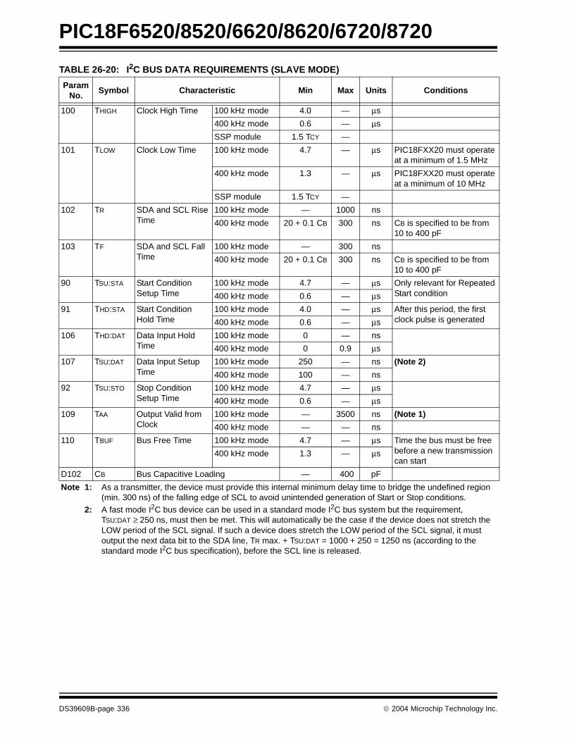
PIC18F6520/8520/6620/8620/6720/8720
TABLE 26-20: I2C BUS DATA REQUIREMENTS (SLAVE MODE)
ParamNo.
Symbol Characteristic Min Max Units Conditions
100 THIGH Clock High Time 100 kHz mode 4.0 — µs
400 kHz mode 0.6 — µs
SSP module 1.5 TCY —
101 TLOW Clock Low Time 100 kHz mode 4.7 — µs PIC18FXX20 must operate at a minimum of 1.5 MHz
400 kHz mode 1.3 — µs PIC18FXX20 must operate at a minimum of 10 MHz
SSP module 1.5 TCY —
102 TR SDA and SCL Rise Time
100 kHz mode — 1000 ns
400 kHz mode 20 + 0.1 CB 300 ns CB is specified to be from 10 to 400 pF
103 TF SDA and SCL Fall Time
100 kHz mode — 300 ns
400 kHz mode 20 + 0.1 CB 300 ns CB is specified to be from 10 to 400 pF
90 TSU:STA Start Condition Setup Time
100 kHz mode 4.7 — µs Only relevant for Repeated Start condition400 kHz mode 0.6 — µs
91 THD:STA Start Condition Hold Time
100 kHz mode 4.0 — µs After this period, the first clock pulse is generated400 kHz mode 0.6 — µs
106 THD:DAT Data Input Hold Time
100 kHz mode 0 — ns
400 kHz mode 0 0.9 µs
107 TSU:DAT Data Input Setup Time
100 kHz mode 250 — ns (Note 2)
400 kHz mode 100 — ns
92 TSU:STO Stop Condition Setup Time
100 kHz mode 4.7 — µs
400 kHz mode 0.6 — µs
109 TAA Output Valid from Clock
100 kHz mode — 3500 ns (Note 1)
400 kHz mode — — ns
110 TBUF Bus Free Time 100 kHz mode 4.7 — µs Time the bus must be free before a new transmission can start
400 kHz mode 1.3 — µs
D102 CB Bus Capacitive Loading — 400 pF
Note 1: As a transmitter, the device must provide this internal minimum delay time to bridge the undefined region (min. 300 ns) of the falling edge of SCL to avoid unintended generation of Start or Stop conditions.
2: A fast mode I2C bus device can be used in a standard mode I2C bus system but the requirement, TSU:DAT ≥ 250 ns, must then be met. This will automatically be the case if the device does not stretch the LOW period of the SCL signal. If such a device does stretch the LOW period of the SCL signal, it must output the next data bit to the SDA line, TR max. + TSU:DAT = 1000 + 250 = 1250 ns (according to the standard mode I2C bus specification), before the SCL line is released.
DS39609B-page 336 2004 Microchip Technology Inc.

PIC18F6520/8520/6620/8620/6720/8720
FIGURE 26-22: MASTER SSP I2C BUS START/STOP BITS TIMING WAVEFORMS
TABLE 26-21: MASTER SSP I2C BUS START/STOP BITS REQUIREMENTS
FIGURE 26-23: MASTER SSP I2C BUS DATA TIMING
Note: Refer to Figure 26-6 for load conditions.
91 93SCL
SDA
StartCondition
StopCondition
90 92
ParamNo.
Symbol Characteristic Min Max Units Conditions
90 TSU:STA Start Condition Setup Time
100 kHz mode 2(TOSC)(BRG + 1) — ns Only relevant for Repeated Start condition400 kHz mode 2(TOSC)(BRG + 1) —
1 MHz mode(1) 2(TOSC)(BRG + 1) —
91 THD:STA Start Condition Hold Time
100 kHz mode 2(TOSC)(BRG + 1) — ns After this period, the first clock pulse is generated400 kHz mode 2(TOSC)(BRG + 1) —
1 MHz mode(1) 2(TOSC)(BRG + 1) —
92 TSU:STO Stop ConditionSetup Time
100 kHz mode 2(TOSC)(BRG + 1) — ns
400 kHz mode 2(TOSC)(BRG + 1) —
1 MHz mode(1) 2(TOSC)(BRG + 1) —
93 THD:STO Stop ConditionHold Time
100 kHz mode 2(TOSC)(BRG + 1) — ns
400 kHz mode 2(TOSC)(BRG + 1) —
1 MHz mode(1) 2(TOSC)(BRG + 1) —
Note 1: Maximum pin capacitance = 10 pF for all I2C pins.
Note: Refer to Figure 26-6 for load conditions.
9091 92
100
101
103
106107
109 109 110
102
SCL
SDAIn
SDAOut
2004 Microchip Technology Inc. DS39609B-page 337

PIC18F6520/8520/6620/8620/6720/8720
TABLE 26-22: MASTER SSP I2C BUS DATA REQUIREMENTS Param
No.Symbol Characteristic Min Max Units Conditions
100 THIGH Clock High Time 100 kHz mode 2(TOSC)(BRG + 1) — ms
400 kHz mode 2(TOSC)(BRG + 1) — ms
1 MHz mode(1) 2(TOSC)(BRG + 1) — ms
101 TLOW Clock Low Time 100 kHz mode 2(TOSC)(BRG + 1) — ms
400 kHz mode 2(TOSC)(BRG + 1) — ms
1 MHz mode(1) 2(TOSC)(BRG + 1) — ms
102 TR SDA and SCL Rise Time
100 kHz mode — 1000 ns CB is specified to be from 10 to 400 pF 400 kHz mode 20 + 0.1 CB 300 ns
1 MHz mode(1) — 300 ns
103 TF SDA and SCL Fall Time
100 kHz mode — 300 ns CB is specified to be from 10 to 400 pF 400 kHz mode 20 + 0.1 CB 300 ns
1 MHz mode(1) — 100 ns
90 TSU:STA Start Condition Setup Time
100 kHz mode 2(TOSC)(BRG + 1) — ms Only relevant for Repeated Start condition400 kHz mode 2(TOSC)(BRG + 1) — ms
1 MHz mode(1) 2(TOSC)(BRG + 1) — ms
91 THD:STA Start Condition Hold Time
100 kHz mode 2(TOSC)(BRG + 1) — ms After this period, the first clock pulse is generated400 kHz mode 2(TOSC)(BRG + 1) — ms
1 MHz mode(1) 2(TOSC)(BRG + 1) — ms
106 THD:DAT Data Input Hold Time
100 kHz mode 0 — ns
400 kHz mode 0 0.9 ms
1 MHz mode(1) TBD — ns
107 TSU:DAT Data Input Setup Time
100 kHz mode 250 — ns (Note 2)
400 kHz mode 100 — ns
1 MHz mode(1) TBD — ns
92 TSU:STO Stop Condition Setup Time
100 kHz mode 2(TOSC)(BRG + 1) — ms
400 kHz mode 2(TOSC)(BRG + 1) — ms
1 MHz mode(1) 2(TOSC)(BRG + 1) — ms
109 TAA Output Valid from Clock
100 kHz mode — 3500 ns
400 kHz mode — 1000 ns
1 MHz mode(1) — — ns
110 TBUF Bus Free Time 100 kHz mode 4.7 — ms Time the bus must be free before a new transmission can start
400 kHz mode 1.3 — ms
1 MHz mode(1) TBD — ms
D102 CB Bus Capacitive Loading — 400 pF
Note 1: Maximum pin capacitance = 10 pF for all I2C pins.
2: A fast mode I2C bus device can be used in a standard mode I2C bus system, but parameter #107 ≥ 250 ns, must then be met. This will automatically be the case if the device does not stretch the LOW period of the SCL signal. If such a device does stretch the LOW period of the SCL signal, it must output the next data bit to the SDA line, parameter #102 + parameter #107 = 1000 + 250 = 1250 ns (for 100 kHz mode), before the SCL line is released.
DS39609B-page 338 2004 Microchip Technology Inc.

PIC18F6520/8520/6620/8620/6720/8720
FIGURE 26-24: USART SYNCHRONOUS TRANSMISSION (MASTER/SLAVE) TIMING
TABLE 26-23: USART SYNCHRONOUS TRANSMISSION REQUIREMENTS
FIGURE 26-25: USART SYNCHRONOUS RECEIVE (MASTER/SLAVE) TIMING
TABLE 26-24: USART SYNCHRONOUS RECEIVE REQUIREMENTS
121 121
120122
RC6/TX1/CK1
RC7/RX1/DT1pin
pin
Note: Refer to Figure 26-6 for load conditions.
ParamNo.
Symbol Characteristic Min Max Units Conditions
120 TCKH2DTV SYNC XMIT (MASTER & SLAVE)Clock High to Data Out Valid PIC18FXX20 — 40 ns
PIC18LFXX20 — 100 ns VDD = 2.0V
121 TCKRF Clock Out Rise Time and Fall Time (Master mode)
PIC18FXX20 — 20 ns
PIC18LFXX20 — 50 ns VDD = 2.0V
122 TDTRF Data Out Rise Time and Fall Time PIC18FXX20 — 20 ns
PIC18LFXX20 — 50 ns VDD = 2.0V
125
126
RC6/TX1/CK1
RC7/RX1/DT1
pin
pin
Note: Refer to Figure 26-6 for load conditions.
ParamNo.
Symbol Characteristic Min Max Units Conditions
125 TDTV2CKL SYNC RCV (MASTER & SLAVE)Data Hold before CK ↓ (DT hold time) 10 — ns
126 TCKL2DTL Data Hold after CK ↓ (DT hold time) 15 — ns
2004 Microchip Technology Inc. DS39609B-page 339

PIC18F6520/8520/6620/8620/6720/8720
TABLE 26-25: A/D CONVERTER CHARACTERISTICS: PIC18FXX20 (INDUSTRIAL, EXTENDED) PIC18LFXX20 (INDUSTRIAL)
FIGURE 26-26: A/D CONVERSION TIMING
ParamNo.
Symbol Characteristic Min Typ Max Units Conditions
A01 NR Resolution — — 10 bit
A03 EIL Integral Linearity Error — — <±1 LSb VREF = VDD = 5.0V
A04 EDL Differential Linearity Error — — <±1 LSb VREF = VDD = 5.0V
A05 EG Gain Error — — <±1 LSb VREF = VDD = 5.0V
A06 EOFF Offset Error — — <±1.5 LSb VREF = VDD = 5.0V
A10 — Monotonicity guaranteed(2) — VSS ≤ VAIN ≤ VREF
A20A20A
VREF Reference Voltage(VREFH – VREFL)
1.8V3V
——
——
VV
VDD < 3.0VVDD ≥ 3.0V
A21 VREFH Reference Voltage High AVSS — AVDD + 0.3V V
A22 VREFL Reference Voltage Low AVSS – 0.3V(5) — VREFH V
A25 VAIN Analog Input Voltage AVSS – 0.3V(5) — AVDD + 0.3V(5) V VDD ≥ 2.5V (Note 3)
A30 ZAIN Recommended Impedance of Analog Voltage Source
— — 2.5 kΩ (Note 4)
A50 IREF VREF Input Current (Note 1) ——
——
5150
µAµA
During VAIN acquisition. During A/D conversion cycle.
Note 1: Vss ≤ VAIN ≤ VREF
2: The A/D conversion result never decreases with an increase in the input voltage and has no missing codes.3: For VDD < 2.5V, VAIN should be limited to <.5 VDD.4: Maximum allowed impedance for analog voltage source is 10 kΩ. This requires higher acquisition times.5: IVDD – AVDDI must be <3.0V and IAVSS – VSSI must be <0.3V.
131
130
132
BSF ADCON0, GO
Q4
A/D CLK
A/D DATA
ADRES
ADIF
GO
SAMPLE
OLD_DATA
SAMPLING STOPPED
DONE
NEW_DATA
(Note 2)
9 8 7 2 1 0
Note 1: If the A/D clock source is selected as RC, a time of TCY is added before the A/D clock starts. This allows the SLEEP instruction to beexecuted.
2: This is a minimal RC delay (typically 100 ns), which also disconnects the holding capacitor from the analog input.
. . . . . .
TCY
DS39609B-page 340 2004 Microchip Technology Inc.

PIC18F6520/8520/6620/8620/6720/8720
TABLE 26-26: A/D CONVERSION REQUIREMENTS
ParamNo.
Symbol Characteristic Min Max Units Conditions
130 TAD A/D Clock Period PIC18FXX20 1.6 20(5) µs TOSC based, VREF ≥ 3.0V
PIC18LFXX20 3.0 20(5) µs TOSC based, VREF full range
PIC18FXX20 2.0 6.0 µs A/D RC mode
PIC18LFXX20 3.0 9.0 µs A/D RC mode
131 TCNV Conversion Time (not including acquisition time) (Note 1)
11 12 TAD
132 TACQ Acquisition Time (Note 3) 1510
——
µsµs
-40°C ≤ Temp ≤ +125°C0°C ≤ Temp ≤ +125°C
135 TSWC Switching Time from Convert → Sample — (Note 4)
136 TAMP Amplifier Settling Time (Note 2) 1 — µs This may be used if the “new” input voltage has not changed by more than 1 LSb (i.e., 5 mV @ 5.12V) from the last sampled voltage (as stated on CHOLD).
Note 1: ADRES register may be read on the following TCY cycle.2: See Section 19.0 “10-Bit Analog-to-Digital Converter (A/D) Module” for minimum conditions when
input voltage has changed more than 1 LSb.3: The time for the holding capacitor to acquire the “New” input voltage when the voltage changes full scale
after the conversion (AVDD to AVSS, or AVSS to AVDD). The source impedance (RS) on the input channels is 50Ω.
4: On the next Q4 cycle of the device clock. 5: The time of the A/D clock period is dependent on the device frequency and the TAD clock divider.
2004 Microchip Technology Inc. DS39609B-page 341

PIC18F6520/8520/6620/8620/6720/8720
NOTES:
DS39609B-page 342 2004 Microchip Technology Inc.

PIC18F6520/8520/6620/8620/6720/8720
27.0 DC AND AC CHARACTERISTICS GRAPHS AND TABLES
“Typical” represents the mean of the distribution at 25°C. “Maximum” or “minimum” represents (mean + 3σ) or (mean –‘3σ) respectively, where σ is a standard deviation, over the whole temperature range.
FIGURE 27-1: TYPICAL IDD vs. FOSC OVER VDD (HS MODE)
FIGURE 27-2: MAXIMUM IDD vs. FOSC OVER VDD (HS MODE) INDUSTRIAL
Note: The graphs and tables provided following this note are a statistical summary based on a limited number ofsamples and are provided for informational purposes only. The performance characteristics listed hereinare not tested or guaranteed. In some graphs or tables, the data presented may be outside the specifiedoperating range (e.g., outside specified power supply range) and therefore, outside the warranted range.
0
2
4
6
8
10
12
14
16
18
20
4 6 8 10 12 14 16 18 20 22 24 26
FOSC (MHz)
IDD
(m
A)
2.0V
2.5V
3.0V
3.5V
4.0V
4.5V
5.0V
5.5V
Typical: statistical mean @ 25°CMaximum: mean + 3σ (-40°C to +125°C) Minimum: mean – 3σ (-40°C to +125°C)
0
2
4
6
8
10
12
14
16
18
20
4 6 8 10 12 14 16 18 20 22 24 26
FOSC (MHz)
IDD
(m
A)
2.0V
2.5V
3.0V
3.5V
4.0V
4.5V
5.0V
5.5V
Typical: statistical mean @ 25°CMaximum: mean + 3σ (-40°C to +85°C) Minimum: mean – 3σ (-40°C to +85°C)
2004 Microchip Technology Inc. DS39609B-page 343
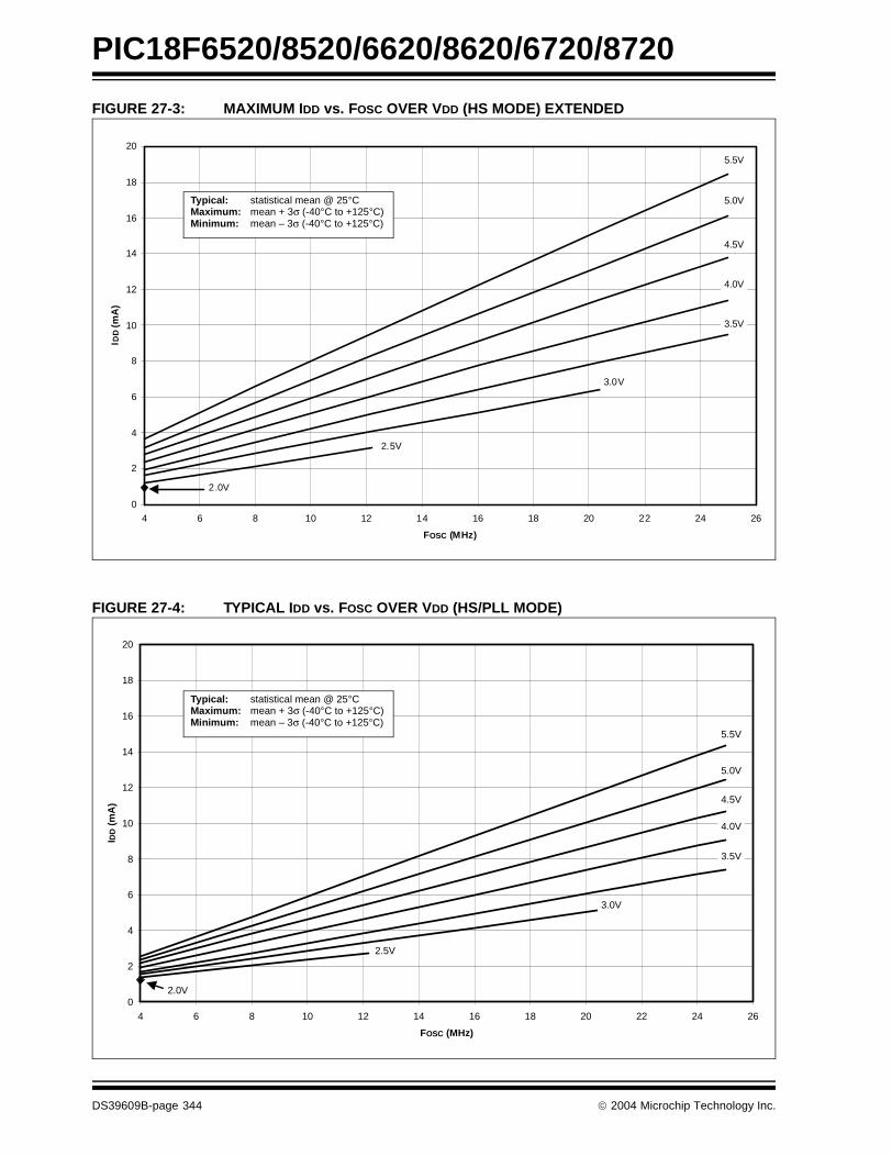
PIC18F6520/8520/6620/8620/6720/8720
FIGURE 27-3: MAXIMUM IDD vs. FOSC OVER VDD (HS MODE) EXTENDED
FIGURE 27-4: TYPICAL IDD vs. FOSC OVER VDD (HS/PLL MODE)
0
2
4
6
8
10
12
14
16
18
20
4 6 8 10 12 14 16 18 20 22 24 26
FOSC (MHz)
IDD (
mA
)
2.0V
2.5V
3.0V
3.5V
4.0V
4.5V
5.0V
5.5V
Typical: statistical mean @ 25°CMaximum: mean + 3σ (-40°C to +125°C) Minimum: mean – 3σ (-40°C to +125°C)
0
2
4
6
8
10
12
14
16
18
20
4 6 8 10 12 14 16 18 20 22 24 26
FOSC (MHz)
IDD
(m
A)
2.0V
2.5V
3.0V
3.5V
4.0V
4.5V
5.0V
5.5V
Typical: statistical mean @ 25°CMaximum: mean + 3σ (-40°C to +125°C) Minimum: mean – 3σ (-40°C to +125°C)
DS39609B-page 344 2004 Microchip Technology Inc.
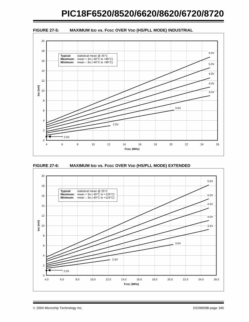
PIC18F6520/8520/6620/8620/6720/8720
FIGURE 27-5: MAXIMUM IDD vs. FOSC OVER VDD (HS/PLL MODE) INDUSTRIAL
FIGURE 27-6: MAXIMUM IDD vs. FOSC OVER VDD (HS/PLL MODE) EXTENDED
0
2
4
6
8
10
12
14
16
18
20
4 6 8 10 12 14 16 18 20 22 24 26
FOSC (MHz)
IDD
(m
A)
2.0V
2.5V
3.0V
3.5V
4.0V
4.5V
5.0V
5.5VTypical: statistical mean @ 25°CMaximum: mean + 3σ (-40°C to +85°C) Minimum: mean – 3σ (-40°C to +85°C)
0
2
4
6
8
10
12
14
16
18
20
4.0 6.0 8.0 10.0 12.0 14.0 16.0 18.0 20.0 22.0 24.0 26.0
FOSC (MHz)
IDD
(m
A)
2.0V
2.5V
3.0V
3.5V
4.0V
4.5V
5.0V
5.5V
Typical: statistical mean @ 25°CMaximum: mean + 3σ (-40°C to +125°C) Minimum: mean – 3σ (-40°C to +125°C)
2004 Microchip Technology Inc. DS39609B-page 345
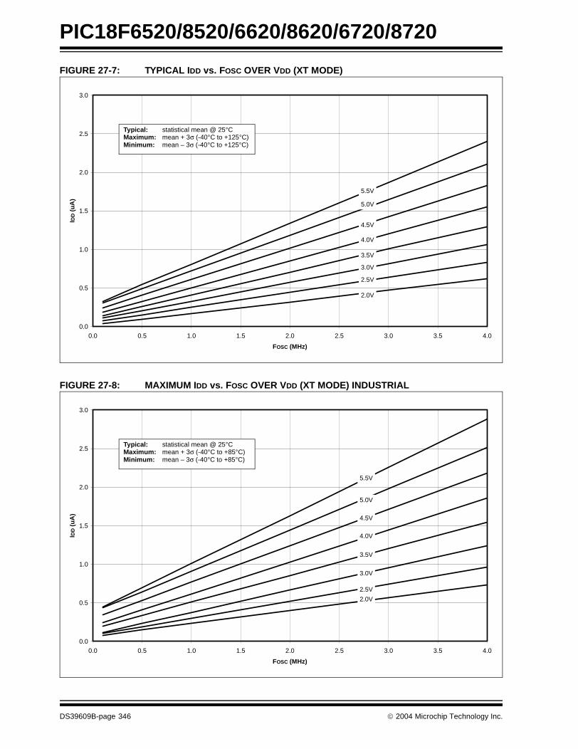
PIC18F6520/8520/6620/8620/6720/8720
FIGURE 27-7: TYPICAL IDD vs. FOSC OVER VDD (XT MODE)
FIGURE 27-8: MAXIMUM IDD vs. FOSC OVER VDD (XT MODE) INDUSTRIAL
0.0
0.5
1.0
1.5
2.0
2.5
3.0
0.0 0.5 1.0 1.5 2.0 2.5 3.0 3.5 4.0
FOSC (MHz)
IDD
(u
A)
4.0V
4.5V
3.0V
3.5V
2.0V
2.5V
5.0V
5.5V
Typical: statistical mean @ 25°CMaximum: mean + 3σ (-40°C to +125°C) Minimum: mean – 3σ (-40°C to +125°C)
0.0
0.5
1.0
1.5
2.0
2.5
3.0
0.0 0.5 1.0 1.5 2.0 2.5 3.0 3.5 4.0
FOSC (MHz)
IDD
(u
A)
4.0V
4.5V
3.0V
3.5V
2.0V
2.5V
5.0V
5.5V
Typical: statistical mean @ 25°CMaximum: mean + 3σ (-40°C to +85°C) Minimum: mean – 3σ (-40°C to +85°C)
DS39609B-page 346 2004 Microchip Technology Inc.

PIC18F6520/8520/6620/8620/6720/8720
FIGURE 27-9: TYPICAL IDD vs. FOSC OVER VDD (LP MODE)
FIGURE 27-10: MAXIMUM IDD vs. FOSC OVER VDD (LP MODE) INDUSTRIAL
0
10
20
30
40
50
60
70
80
90
100
0 10 20 30 40 50 60 70 80 90 100
FOSC (kHz)
IDD
(u
A)
2.0V
2.5V
3.0V
3.5V
4.0V
4.5V
5.0V
5.5V
Typical: statistical mean @ 25°CMaximum: mean + 3σ (-40°C to +125°C) Minimum: mean – 3σ (-40°C to +125°C)
0
20
40
60
80
100
120
0 10 20 30 40 50 60 70 80 90 100
FOSC (kHz)
IDD
(u
A)
2.0V
2.5V
3.0V
3.5V
4.0V
4.5V
5.0V
5.5V
Typical: statistical mean @ 25°CMaximum: mean + 3σ (-40°C to +85°C) Minimum: mean – 3σ (-40°C to +85°C)
2004 Microchip Technology Inc. DS39609B-page 347

PIC18F6520/8520/6620/8620/6720/8720
FIGURE 27-11: MAXIMUM IDD vs. FOSC OVER VDD (LP MODE) EXTENDED
FIGURE 27-12: TYPICAL IDD vs. FOSC OVER VDD (EC MODE)
0
50
100
150
200
250
300
0 10 20 30 40 50 60 70 80 90 100
FOSC (kHz)
IDD
(u
A)
2.0V
2.5V
3.0V
3.5V
4.0V
4.5V
5.0V
5.5VTypical: statistical mean @ 25°CMaximum: mean + 3σ (-40°C to +125°C) Minimum: mean – 3σ (-40°C to +125°C)
0
2
4
6
8
10
12
14
16
18
4 6 8 10 12 14 16 18 20 22 24 26
FOSC (MHz)
IDD
(m
A)
4.0V
4.5V
3.0V
3.5V
2.0V
2.5V
5.0V
5.5V
Typical: statistical mean @ 25°CMaximum: mean + 3σ (-40°C to +125°C) Minimum: mean – 3σ (-40°C to +125°C)
DS39609B-page 348 2004 Microchip Technology Inc.

PIC18F6520/8520/6620/8620/6720/8720
FIGURE 27-13: MAXIMUM IDD vs. FOSC OVER VDD (EC MODE)
FIGURE 27-14: MAXIMUM IPD vs. VDD OVER TEMPERATURE
0
2
4
6
8
10
12
14
16
18
4 6 8 10 12 14 16 18 20 22 24 26
FOSC (MHz)
IDD
(m
A)
5.0V
5.5V
4.0V
4.5V
3.0V
3.5V
2.0V
2.5V
Typical: statistical mean @ 25°CMaximum: mean + 3σ (-40°C to +125°C) Minimum: mean – 3σ (-40°C to +125°C)
0.01
0.1
1
10
100
2.0 2.5 3.0 3.5 4.0 4.5 5.0 5.5
VDD (V)
IPD
(u
A)
Typ(25°C)
Max(-40°C:+85°C)
Max(-40°C:+125°C)
Typical: statistical mean @ 25°CMaximum: mean + 3σ (-40°C to +125°C) Minimum: mean – 3σ (-40°C to +125°C)
2004 Microchip Technology Inc. DS39609B-page 349

PIC18F6520/8520/6620/8620/6720/8720
FIGURE 27-15: TYPICAL AND MAXIMUM IPD vs. VDD OVER TEMPERATURE (TIMER1 AS MAIN OSCILLATOR, 32.768 kHz, C1 AND C2 = 47 pF)
FIGURE 27-16: TYPICAL AND MAXIMUM ∆IWDT vs. VDD OVER TEMPERATURE (WDT ENABLED)
1
10
100
1000
2.0 2.5 3.0 3.5 4.0 4.5 5.0 5.5
VDD (V)
IPD
(u
A)
Typ(25°C)
Max(-40°C:+85°C)
Max(-40°C:+125°C)
Typical: statistical mean @ 25°CMaximum: mean + 3σ (-40°C to +125°C) Minimum: mean – 3σ (-40°C to +125°C)
0.1
1
10
100
1000
2.0 2.5 3.0 3.5 4.0 4.5 5.0 5.5
VDD (V)
IPD
(u
A)
Typ(25°C)
Max(-40°C:+85°C)
Max(-40°C:+125°C)
Typical: statistical mean @ 25°CMaximum: mean + 3σ (-40°C to +125°C) Minimum: mean – 3σ (-40°C to +125°C)
DS39609B-page 350 2004 Microchip Technology Inc.

PIC18F6520/8520/6620/8620/6720/8720
FIGURE 27-17: TYPICAL IDD vs. FOSC OVER VDD (EC MODE)
FIGURE 27-18: MAXIMUM IDD vs. FOSC OVER VDD (EC MODE)
0.00
0.05
0.10
0.15
0.20
0.25
0.30
0.35
0.40
0.45
0.50
0.55
0.00 0.02 0.04 0.06 0.08 0.10 0.12 0.14 0.16 0.18 0.20
FOSC (MHz)
IDD
(m
A)
4.0V
4.5V
3.0V
3.5V
2.0V
2.5V
5.0V
5.5V
Typical: statistical mean @ 25°CMaximum: mean + 3σ (-40°C to +125°C) Minimum: mean – 3σ (-40°C to +125°C)
0.00
0.05
0.10
0.15
0.20
0.25
0.30
0.35
0.40
0.45
0.50
0.55
0.00 0.02 0.04 0.06 0.08 0.10 0.12 0.14 0.16 0.18 0.20
FOSC (MHz)
IDD
(m
A)
4.0V
4.5V
3.0V
3.5V
2.0V
2.5V
5.0V
5.5VTypical: statistical mean @ 25°CMaximum: mean + 3σ (-40°C to +125°C) Minimum: mean – 3σ (-40°C to +125°C)
2004 Microchip Technology Inc. DS39609B-page 351

PIC18F6520/8520/6620/8620/6720/8720
FIGURE 27-19: TYPICAL IDD vs. FOSC OVER VDD (EC MODE) (PIC18F8520 DEVICES ONLY)
FIGURE 27-20: MAXIMUM IDD vs. FOSC OVER VDD (EC MODE) INDUSTRIAL (PIC18F8520 DEVICES ONLY)
0
5
10
15
20
25
30
4 8 12 16 20 24 28 32 36 40
FOSC (MHz)
IDD
(m
A)
4.0V
4.5V
3.0V
3.5V
2.0V
2.5V
5.0V
5.5V
4.2V
Typical: statistical mean @ 25°CMaximum: mean + 3σ (-40°C to +125°C) Minimum: mean – 3σ (-40°C to +125°C)
0
5
10
15
20
25
30
4 8 12 16 20 24 28 32 36 40
FOSC (MHz)
IDD
(m
A)
5.0V
5.5V
4.2V
4.5V
3.0V
3.5V
2.0V
2.5V
4.0V
Typical: statistical mean @ 25°CMaximum: mean + 3σ (-40°C to +85°C) Minimum: mean – 3σ (-40°C to +85°C)
DS39609B-page 352 2004 Microchip Technology Inc.

PIC18F6520/8520/6620/8620/6720/8720
FIGURE 27-21: MAXIMUM IDD vs. FOSC OVER VDD (EC MODE) EXTENDED (PIC18F8520 DEVICES ONLY)
FIGURE 27-22: TYPICAL IDD vs. FOSC OVER VDD (HS/PLL MODE)(PIC18F8520 DEVICES ONLY)
0
2
4
6
8
10
12
14
16
18
20
4 6 8 10 12 14 16 18 20 22 24 26
FOSC (MHz)
IDD
(m
A)
5.0V
5.5V
4.2V
4.5V
3.0V
3.5V
2.0V
2.5V
4.0V
Typical: statistical mean @ 25°CMaximum: mean + 3σ (-40°C to +125°C) Minimum: mean – 3σ (-40°C to +125°C)
0
3
6
9
12
15
18
21
24
27
30
4 8 12 16 20 24 28 32 36 40
FOSC (MHz)
IDD
(m
A)
2.0V
2.5V
3.0V
3.5V
4.0V
4.5V
5.0V
5.5V
4.2V
Typical: statistical mean @ 25°CMaximum: mean + 3σ (-40°C to +125°C) Minimum: mean – 3σ (-40°C to +125°C)
2004 Microchip Technology Inc. DS39609B-page 353

PIC18F6520/8520/6620/8620/6720/8720
FIGURE 27-23: MAXIMUM IDD vs. FOSC OVER VDD (HS/PLL MODE) INDUSTRIAL(PIC18F8520 DEVICES ONLY)
FIGURE 27-24: MAXIMUM IDD vs. FOSC OVER VDD (HS/PLL MODE) EXTENDED(PIC18F8520 DEVICES ONLY)
0
3
6
9
12
15
18
21
24
27
30
4 8 12 16 20 24 28 32 36 40
FOSC (MHz)
IDD
(m
A)
2.0V
2.5V
3.0V
3.5V
4.0V
4.5V
5.0V
5.5V
4.2V
Typical: statistical mean @ 25°CMaximum: mean + 3σ (-40°C to +85°C) Minimum: mean – 3σ (-40°C to +85°C)
0
2
4
6
8
10
12
14
16
18
20
4 6 8 10 12 14 16 18 20 22 24 26
FOSC (MHz)
IDD
(m
A)
2.0V
2.5V
3.0V
3.5V
4.0V
4.5V
5.0V
5.5V
4.2V
Typical: statistical mean @ 25°CMaximum: mean + 3σ (-40°C to +125°C) Minimum: mean – 3σ (-40°C to +125°C)
DS39609B-page 354 2004 Microchip Technology Inc.

PIC18F6520/8520/6620/8620/6720/8720
FIGURE 27-25: A/D NONLINEARITY vs. VREFH (VDD = VREFH, -40°C TO +125°C)
FIGURE 27-26: A/D NONLINEARITY vs. VREFH (VDD = 5V, -40°C TO +125°C)
0
0.5
1
1.5
2
2.5
3
3.5
4
2 2.5 3 3.5 4 4.5 5 5.5
VDD and VREFH (V)
Dif
fere
nti
al o
r In
teg
ral N
on
linea
rity
(L
SB
)
-40C
25C
85C
125C
-40°C
+25°C
+85°C
+125°C
0
0.5
1
1.5
2
2.5
3
2 2.5 3 3.5 4 4.5 5 5.5
VREFH (V)
Dif
fere
nti
al o
r In
teg
ral N
on
linea
rilt
y (L
SB
)
Max (-40C to 125C)
Typ (25C)Typ (+25°C)
Max (-40°C to +125°C)
2004 Microchip Technology Inc. DS39609B-page 355

PIC18F6520/8520/6620/8620/6720/8720
NOTES:
DS39609B-page 356 2004 Microchip Technology Inc.

PIC18F6520/8520/6620/8620/6720/8720
28.0 PACKAGING INFORMATION
28.1 Package Marking Information
64-Lead TQFP
XXXXXXXXXXXXXXXXXXXXXXXXXXXXXX
YYWWNNN
Example
PIC18F6620-I/PT
0410017
80-Lead TQFP
XXXXXXXXXXXXXXXXXXXXXXXX
YYWWNNN
Example
PIC18F8720-E/PT
0410017
Legend: XX...X Customer specific information*Y Year code (last digit of calendar year)YY Year code (last 2 digits of calendar year)WW Week code (week of January 1 is week ‘01’)NNN Alphanumeric traceability code
Note: In the event the full Microchip part number cannot be marked on one line, it willbe carried over to the next line thus limiting the number of available charactersfor customer specific information.
* Standard PICmicro device marking consists of Microchip part number, year code, week code, andtraceability code. For PICmicro device marking beyond this, certain price adders apply. Please checkwith your Microchip Sales Office. For QTP devices, any special marking adders are included in QTPprice.
2004 Microchip Technology Inc. DS39609B-page 357

PIC18F6520/8520/6620/8620/6720/8720
28.2 Package Details The following sections give the technical details of the packages.
64-Lead Plastic Thin Quad Flatpack (PT) 10x10x1 mm Body, 1.0/0.10 mm Lead Form (TQFP)
* Controlling Parameter
Notes:Dimensions D1 and E1 do not include mold flash or protrusions. Mold flash or protrusions shall not exceed.010” (0.254mm) per side.JEDEC Equivalent: MS-026Drawing No. C04-085
1510515105βMold Draft Angle Bottom1510515105αMold Draft Angle Top
0.270.220.17.011.009.007BLead Width0.230.180.13.009.007.005cLead Thickness
1616n1Pins per Side
10.1010.009.90.398.394.390D1Molded Package Length10.1010.009.90.398.394.390E1Molded Package Width12.2512.0011.75.482.472.463DOverall Length12.2512.0011.75.482.472.463EOverall Width
73.5073.50φFoot Angle
0.750.600.45.030.024.018LFoot Length0.250.150.05.010.006.002A1Standoff §1.051.000.95.041.039.037A2Molded Package Thickness1.201.101.00.047.043.039AOverall Height
0.50.020pPitch6464nNumber of Pins
MAXNOMMINMAXNOMMINDimension LimitsMILLIMETERS*INCHESUnits
c
21
n
DD1
B
p
#leads=n1
E1
E
A2
A1
A
L
CH x 45°
βφ
α
(F)
Footprint (Reference) (F) .039 1.00
Pin 1 Corner Chamfer CH .025 .035 .045 0.64 0.89 1.14
§ Significant Characteristic
DS39609B-page 358 2004 Microchip Technology Inc.

PIC18F6520/8520/6620/8620/6720/8720
80-Lead Plastic Thin Quad Flatpack (PT) 12x12x1 mm Body, 1.0/0.10 mm Lead Form (TQFP)
* Controlling Parameter
Notes:Dimensions D1 and E1 do not include mold flash or protrusions. Mold flash or protrusions shall not exceed .010” (0.254mm) per side.JEDEC Equivalent: MS-026Drawing No. C04-092
1.101.00.043.039
1.140.890.64.045.035.025CHPin 1 Corner Chamfer
1.00.039(F)Footprint (Reference)
(F)
EE1
#leads=n1
p
B
D1 D
n
12
φ
c
βL
A
A1A2
α
Units INCHES MILLIMETERS*Dimension Limits MIN NOM MAX MIN NOM MAX
Number of Pins n 80 80Pitch p .020 0.50
Overall Height A .047 1.20Molded Package Thickness A2 .037 .039 .041 0.95 1.00 1.05Standoff § A1 .002 .004 .006 0.05 0.10 0.15Foot Length L .018 .024 .030 0.45 0.60 0.75
Foot Angle φ 0 3.5 7 0 3.5 7Overall Width E .541 .551 .561 13.75 14.00 14.25Overall Length D .541 .551 .561 13.75 14.00 14.25Molded Package Width E1 .463 .472 .482 11.75 12.00 12.25Molded Package Length D1 .463 .472 .482 11.75 12.00 12.25
Pins per Side n1 20 20
Lead Thickness c .004 .006 .008 0.09 0.15 0.20Lead Width B .007 .009 .011 0.17 0.22 0.27
Mold Draft Angle Top α 5 10 15 5 10 15Mold Draft Angle Bottom β 5 10 15 5 10 15
CH x 45°
§ Significant Characteristic
2004 Microchip Technology Inc. DS39609B-page 359

PIC18F6520/8520/6620/8620/6720/8720
NOTES:
DS39609B-page 360 2004 Microchip Technology Inc.
PIC18F6520/8520/6620/8620/6720/8720
APPENDIX A: REVISION HISTORY
Revision A (January 2003)
Original data sheet for the PIC18FXX20 family whichincludes PIC18F6520, PIC18F6620, PIC18F6720,PIC18F8520, PIC18F8620 and PIC18F8720 devices.
This data sheet is based on the previous PIC18FXX20Data Sheet (DS39580).
Revision B (January 2004)
This revision includes the DC and AC CharacteristicsGraphs and Tables. The Electrical Specifications inSection 26.0 “Electrical Characteristics” have beenupdated and there have been minor corrections to thedata sheet text.
APPENDIX B: DEVICE DIFFERENCES
The differences between the devices listed in this datasheet are shown in Table B-1.
TABLE B-1: DEVICE DIFFERENCES
Feature PIC18F6520 PIC18F6620 PIC18F6720 PIC18F8520 PIC18F8620 PIC18F8720
On-Chip Program Memory (Kbytes)
32 64 128 32 64 128
Data Memory (bytes) 2048 3840 3840 2048 3840 3840
Boot Block (bytes) 2048 512 512 2048 512 512
Timer1 Low-Power Option Yes No No Yes No No
I/O Ports Ports A, B, C, D, E, F, G
Ports A, B, C, D, E, F, G
Ports A, B, C, D, E, F, G
Ports A, B, C, D, E, F, G, H, J
Ports A, B, C, D, E, F, G, H, J
Ports A, B, C, D, E, F, G, H, J
A/D Channels 12 12 12 16 16 16
External Memory Interface No No No Yes Yes Yes
Maximum Operating Frequency (MHz)
40 25 25 40 25 25
Package Types 64-pin TQFP 64-pin TQFP 64-pin TQFP 80-pin TQFP 80-pin TQFP 80-pin TQFP
2004 Microchip Technology Inc. DS39609B-page 361

PIC18F6520/8520/6620/8620/6720/8720
APPENDIX C: CONVERSION CONSIDERATIONS
This appendix discusses the considerations forconverting from previous versions of a device to theones listed in this data sheet. Typically, these changesare due to the differences in the process technologyused. An example of this type of conversion is from aPIC17C756 to a PIC18F8720.
Not Currently Available
APPENDIX D: MIGRATION FROM MID-RANGE TO ENHANCED DEVICES
A detailed discussion of the differences between themid-range MCU devices (i.e., PIC16CXXX) and theenhanced devices (i.e., PIC18FXXX) is provided inAN716, “Migrating Designs from PIC16C74A/74B toPIC18C442”. The changes discussed, while devicespecific, are generally applicable to all mid-range toenhanced device migrations.
This Application Note is available as Literature NumberDS00716.
DS39609B-page 362 2004 Microchip Technology Inc.

PIC18F6520/8520/6620/8620/6720/8720
APPENDIX E: MIGRATION FROM HIGH-END TO ENHANCED DEVICES
A detailed discussion of the migration pathway and dif-ferences between the high-end MCU devices (i.e.,PIC17CXXX) and the enhanced devices (i.e.,PIC18FXXXX) is provided in AN726, “PIC17CXXX toPIC18CXXX Migration”. This Application Note isavailable as Literature Number DS00726.
2004 Microchip Technology Inc. DS39609B-page 363

PIC18F6520/8520/6620/8620/6720/8720
NOTES:
DS39609B-page 364 2004 Microchip Technology Inc.

PIC18F6520/8520/6620/8620/6720/8720
INDEX
AA/D ................................................................................... 213
A/D Converter Interrupt, Configuring ....................... 217Acquisition Requirements ........................................ 218Acquisition Time ....................................................... 218ADCON0 Register .................................................... 213ADCON1 Register .................................................... 213ADCON2 Register .................................................... 213ADRESH Register ............................................ 213, 215ADRESL Register ............................................ 213, 215Analog Port Pins ...................................................... 128Analog Port Pins, Configuring .................................. 219Associated Register Summary ................................. 221Calculating Minimum Required
Acquisition Time (Example) ............................. 218CCP2 Trigger ........................................................... 220Configuring the Module ............................................ 217Conversion Clock (TAD) ........................................... 219Conversion Requirements ....................................... 341Conversion Status (GO/DONE Bit) .......................... 215Conversion TAD Cycles ............................................ 220Conversions ............................................................. 220Converter Characteristics ........................................ 340Equations ................................................................. 218Minimum Charging Time .......................................... 218Special Event Trigger (CCP) .................................... 152Special Event Trigger (CCP2) .................................. 220TAD vs. Device Operating Frequencies (Table) ....... 219
Absolute Maximum Ratings ............................................. 307AC (Timing) Characteristics ............................................. 320
Load Conditions for Device Timing Specifications ....................................... 321
Parameter Symbology ............................................. 320Temperature and Voltage Specifications ................. 321Timing Conditions .................................................... 321
ACKSTAT Status Flag ..................................................... 187ADCON0 Register ............................................................ 213
GO/DONE Bit ........................................................... 215ADCON1 Register ............................................................ 213ADCON2 Register ............................................................ 213ADDLW ............................................................................ 265Addressable Universal Synchronous Asynchronous
Receiver Transmitter (USART) ................................ 197ADDWF ............................................................................ 265ADDWFC ......................................................................... 266ADRESH Register .................................................... 213, 215ADRESL Register .................................................... 213, 215Analog-to-Digital Converter. See A/D.ANDLW ............................................................................ 266ANDWF ............................................................................ 267Assembler
MPASM Assembler .................................................. 301
BBaud Rate Generator ....................................................... 183BC .................................................................................... 267BCF .................................................................................. 268BF Status Flag ................................................................. 187Block Diagrams
16-bit Byte Select Mode ............................................. 7516-bit Byte Write Mode .............................................. 7316-bit Word Write Mode ............................................. 74A/D ........................................................................... 216
Analog Input Model .................................................. 217Baud Rate Generator .............................................. 183Capture Mode Operation ......................................... 151Comparator Analog Input Model .............................. 227Comparator I/O Operating Modes (Diagram) .......... 224Comparator Output .................................................. 226Comparator Voltage Reference ............................... 230Compare Mode Operation ....................................... 152Low-Voltage Detect (LVD) ....................................... 234Low-Voltage Detect (LVD) with External Input ........ 234MSSP (I2C Master Mode) ........................................ 181MSSP (I2C Mode) .................................................... 166MSSP (SPI Mode) ................................................... 157On-Chip Reset Circuit ................................................ 29PIC18F6X20 Architecture ............................................ 9PIC18F8X20 Architecture .......................................... 10PLL ............................................................................ 23PORT/LAT/TRIS Operation ..................................... 103PORTA
RA3:RA0 and RA5 Pins ................................... 104RA4/T0CKI Pin ................................................ 104RA6 Pin (as I/O) .............................................. 104
PORTBRB2:RB0 Pins .................................................. 107RB3 Pin ........................................................... 107RB7:RB4 Pins .................................................. 106
PORTC (Peripheral Output Override) ...................... 109PORTD and PORTE
Parallel Slave Port ........................................... 128PORTD in I/O Port Mode ......................................... 111PORTD in System Bus Mode .................................. 112PORTE in I/O Mode ................................................. 115PORTE in System Bus Mode .................................. 115PORTF
RF1/AN6/C2OUT and RF2/AN5/C1OUT Pins ............................ 117
RF6/RF3 and RF0 Pins ................................... 118RF7 Pin ........................................................... 118
PORTG (Peripheral Output Override) ..................... 120PORTH
RH3:RH0 Pins in System Bus Mode ....... 123RH3:RH0 Pins in I/O Mode .............................. 122RH7:RH4 Pins in I/O Mode .............................. 122
PORTJRJ4:RJ0 Pins in System Bus Mode ................. 126RJ7:RJ6 Pins in System Bus Mode ................. 126
PORTJ in I/O Mode ................................................. 125PWM Operation (Simplified) .................................... 154Reads from Flash Program Memory ......................... 65Single Comparator ................................................... 225Table Read Operation ............................................... 61Table Write Operation ............................................... 62Table Writes to Flash Program Memory .................... 67Timer0 in 16-bit Mode .............................................. 132Timer0 in 8-bit Mode ................................................ 132Timer1 ..................................................................... 136Timer1 (16-bit R/W Mode) ....................................... 136Timer2 ..................................................................... 142Timer3 ..................................................................... 144Timer3 in 16-bit R/W Mode ...................................... 144Timer4 ..................................................................... 148USART Receive ...................................................... 206
2004 Microchip Technology Inc. DS39609B-page 365

PIC18F6520/8520/6620/8620/6720/8720
USART Transmit ...................................................... 204Voltage Reference Output Buffer Example .............. 231Watchdog Timer ....................................................... 251
BN .................................................................................... 268BNC .................................................................................. 269BNN .................................................................................. 269BNOV ............................................................................... 270BNZ .................................................................................. 270BOR. See Brown-out Reset.BOV .................................................................................. 273BRA .................................................................................. 271BRG. See Baud Rate Generator.Brown-out Reset (BOR) ..................................................... 30BSF .................................................................................. 271BTFSC ............................................................................. 272BTFSS .............................................................................. 272BTG .................................................................................. 273BZ ..................................................................................... 274
CC Compilers
MPLAB C17 ............................................................. 302MPLAB C18 ............................................................. 302MPLAB C30 ............................................................. 302
CALL ................................................................................ 274Capture (CCP Module) ..................................................... 151
Associated Registers ............................................... 153CCP Pin Configuration ............................................. 151CCPR1H:CCPR1L Registers ................................... 151Software Interrupt .................................................... 151Timer1/Timer3 Mode Selection ................................ 151
Capture/Compare/PWM (CCP) ........................................ 149Capture Mode. See Capture.CCP Mode and Timer Resources ............................ 150CCPRxH Register .................................................... 150CCPRxL Register ..................................................... 150Compare Mode. See Compare.Interconnect Configurations ..................................... 150Module Configuration ............................................... 150PWM Mode. See PWM.
Capture/Compare/PWM Requirements (All CCP Modules) ................................................... 329
CLKO and I/O Timing Requirements ....................... 324, 325Clocking Scheme/Instruction Cycle .................................... 44CLRF ................................................................................ 275CLRWDT .......................................................................... 275Code Examples
16 x 16 Signed Multiply Routine ................................ 8616 x 16 Unsigned Multiply Routine ............................ 868 x 8 Signed Multiply Routine .................................... 858 x 8 Unsigned Multiply Routine ................................ 85Changing Between Capture Prescalers ................... 151Data EEPROM Read ................................................. 81Data EEPROM Refresh Routine ................................ 82Data EEPROM Write ................................................. 81Erasing a Flash Program Memory Row ..................... 66Fast Register Stack .................................................... 44How to Clear RAM (Bank 1)
Using Indirect Addressing .................................. 57Implementing a Real-Time Clock Using a
Timer1 Interrupt Service .................................. 139Initializing PORTA .................................................... 103Initializing PORTB .................................................... 106Initializing PORTC .................................................... 109Initializing PORTD .................................................... 111Initializing PORTE .................................................... 114
Initializing PORTF .................................................... 117Initializing PORTG ................................................... 120Initializing PORTH ................................................... 122Initializing PORTJ .................................................... 125Loading the SSPBUF (SSPSR) Register ................. 160Reading a Flash Program Memory Word .................. 65Saving Status, WREG and BSR Registers
in RAM ............................................................. 102Writing to Flash Program Memory ....................... 68–69
Code Protection ............................................................... 239COMF .............................................................................. 276Comparator ...................................................................... 223
Analog Input Connection Considerations ................ 227Associated Registers ............................................... 228Configuration ........................................................... 224Effects of a Reset .................................................... 227Interrupts ................................................................. 226Operation ................................................................. 225Operation During Sleep ........................................... 227Outputs .................................................................... 225Reference ................................................................ 225
External Signal ................................................ 225Internal Signal .................................................. 225
Response Time ........................................................ 225Comparator Specifications ............................................... 317Comparator Voltage Reference ....................................... 229
Accuracy and Error .................................................. 230Associated Registers ............................................... 231Configuring .............................................................. 229Connection Considerations ...................................... 230Effects of a Reset .................................................... 230Operation During Sleep ........................................... 230
Compare (CCP Module) .................................................. 152Associated Registers ............................................... 153CCP Pin Configuration ............................................. 152CCPR1 Register ...................................................... 152Software Interrupt .................................................... 152Special Event Trigger .............................. 138, 145, 152Timer1/Timer3 Mode Selection ................................ 152
Compare (CCP2 Module)Special Event Trigger .............................................. 220
Configuration Bits ............................................................ 239Context Saving During Interrupts ..................................... 102Control Registers
EECON1 and EECON2 ............................................. 62TABLAT (Table Latch) Register ................................. 64TBLPTR (Table Pointer) Register .............................. 64
Conversion Considerations .............................................. 362CPFSEQ .......................................................................... 276CPFSGT .......................................................................... 277CPFSLT ........................................................................... 277
DData EEPROM Memory
Associated Registers ................................................. 83EEADR Register ........................................................ 79EEADRH Register ..................................................... 79EECON1 Register ...................................................... 79EECON2 Register ...................................................... 79Operation During Code-Protect ................................. 82Protection Against Spurious Write ............................. 82Reading ..................................................................... 81Using ......................................................................... 82Write Verify ................................................................ 82Writing ....................................................................... 81
DS39609B-page 366 2004 Microchip Technology Inc.

PIC18F6520/8520/6620/8620/6720/8720
Data Memory ..................................................................... 47General Purpose Registers ........................................ 47Map for PIC18FX520 Devices ................................... 48Map for PIC18FX620/X720 Devices .......................... 49Special Function Registers ........................................ 47
DAW ................................................................................. 278DC and AC Characteristics
Graphs and Tables .................................................. 343DC Characteristics
PIC18FXX20 (Industrial and Extended), PIC18LFXX20 (Industrial) ................................ 315
Power-Down and Supply Current ............................ 311Supply Voltage ......................................................... 310
DCFSNZ .......................................................................... 279DECF ............................................................................... 278DECFSZ ........................................................................... 279Demonstration Boards
PICDEM 1 ................................................................ 304PICDEM 17 .............................................................. 304PICDEM 18R ........................................................... 305PICDEM 2 Plus ........................................................ 304PICDEM 3 ................................................................ 304PICDEM 4 ................................................................ 304PICDEM LIN ............................................................ 305PICDEM USB ........................................................... 305PICDEM.net Internet/Ethernet ................................. 304
Development Support ...................................................... 301Device Differences ........................................................... 361Direct Addressing ............................................................... 58
Direct Addressing ....................................................... 56
EElectrical Characteristics .................................................. 307Errata ................................................................................... 5Evaluation and Programming Tools ................................. 305Example SPI Mode Requirements
(Master Mode, CKE = 0) .......................................... 331Example SPI Mode Requirements
(Master Mode, CKE = 1) .......................................... 332Example SPI Mode Requirements
(Slave Mode, CKE = 0) ............................................ 333Example SPI Slave Mode Requirements (CKE = 1) ........ 334Extended Microcontroller Mode ......................................... 71External Clock Timing Requirements ............................... 322External Memory Interface ................................................. 71
16-bit Byte Select Mode ............................................. 7516-bit Byte Write Mode .............................................. 7316-bit Mode ................................................................ 7316-bit Mode Timing .................................................... 7616-bit Word Write Mode ............................................. 74PIC18F8X20 External Bus - I/O Port Functions ......... 72Program Memory Modes and
External Memory Interface ................................. 71
FFirmware Instructions ....................................................... 259Flash Program Memory ..................................................... 61
Associated Registers ................................................. 69Control Registers ....................................................... 62Erase Sequence ........................................................ 66Erasing ....................................................................... 66Operation During Code-Protect ................................. 69Reading ...................................................................... 65Table Pointer
Boundaries Based on Operation ........................ 64Table Pointer Boundaries .......................................... 64
Table Reads and Table Writes .................................. 61Write Sequence ......................................................... 67Writing To .................................................................. 67
Protection Against Spurious Writes ................... 69Unexpected Termination ................................... 69Write Verify ........................................................ 69
GGeneral Call Address Support ......................................... 180GOTO .............................................................................. 280
HHardware Multiplier ............................................................ 85
Introduction ................................................................ 85Operation ................................................................... 85Performance Comparison .......................................... 85
HS/PLL .............................................................................. 23
II/O Ports .......................................................................... 103I2C Bus Data Requirements (Slave Mode) ...................... 336I2C Bus Start/Stop Bits Requirements (Slave Mode) ....... 335I2C Mode
General Call Address Support ................................. 180Master Mode
Operation ......................................................... 182Read/Write Bit Information (R/W Bit) ............... 170, 171Serial Clock (RC3/SCK/SCL) .................................. 171
ID Locations ............................................................. 239, 257INCF ................................................................................ 280INCFSZ ............................................................................ 281In-Circuit Debugger .......................................................... 257
Resources (Table) ................................................... 257In-Circuit Serial Programming (ICSP) ...................... 239, 257Indirect Addressing ............................................................ 58
INDF and FSR Registers ........................................... 57Operation ................................................................... 57
Indirect Addressing Operation ........................................... 58Indirect File Operand ......................................................... 47INFSNZ ............................................................................ 281Instruction Cycle ................................................................ 44Instruction Flow/Pipelining ................................................. 45Instruction Format ............................................................ 261Instruction Set .................................................................. 259
ADDLW .................................................................... 265ADDWF ................................................................... 265ADDWFC ................................................................. 266ANDLW .................................................................... 266ANDWF ................................................................... 267BC ............................................................................ 267BCF ......................................................................... 268BN ............................................................................ 268BNC ......................................................................... 269BNN ......................................................................... 269BNOV ...................................................................... 270BNZ ......................................................................... 270BOV ......................................................................... 273BRA ......................................................................... 271BSF .......................................................................... 271BTFSC ..................................................................... 272BTFSS ..................................................................... 272BTG ......................................................................... 273BZ ............................................................................ 274CALL ........................................................................ 274CLRF ....................................................................... 275CLRWDT ................................................................. 275
2004 Microchip Technology Inc. DS39609B-page 367

PIC18F6520/8520/6620/8620/6720/8720
COMF ...................................................................... 276CPFSEQ .................................................................. 276CPFSGT .................................................................. 277CPFSLT ................................................................... 277DAW ......................................................................... 278DCFSNZ .................................................................. 279DECF ....................................................................... 278DECFSZ ................................................................... 279GOTO ...................................................................... 280INCF ......................................................................... 280INCFSZ .................................................................... 281INFSNZ .................................................................... 281IORLW ..................................................................... 282IORWF ..................................................................... 282LFSR ........................................................................ 283MOVF ....................................................................... 283MOVFF .................................................................... 284MOVLB .................................................................... 284MOVLW ................................................................... 285MOVWF ................................................................... 285MULLW .................................................................... 286MULWF .................................................................... 286NEGF ....................................................................... 287NOP ......................................................................... 287POP ......................................................................... 288PUSH ....................................................................... 288RCALL ..................................................................... 289RESET ..................................................................... 289RETFIE .................................................................... 290RETLW .................................................................... 290RETURN .................................................................. 291RLCF ........................................................................ 291RLNCF ..................................................................... 292RRCF ....................................................................... 292RRNCF .................................................................... 293SETF ........................................................................ 293SLEEP ..................................................................... 294SUBFWB .................................................................. 294SUBLW .................................................................... 295SUBWF .................................................................... 295SUBWFB .................................................................. 296SWAPF .................................................................... 296TBLRD ..................................................................... 297TBLWT ..................................................................... 298TSTFSZ ................................................................... 299XORLW .................................................................... 299XORWF .................................................................... 300Summary Table ........................................................ 262INT Interrupt (RB0/INT). See Interrupt Sources.INTCON Registers ............................................................. 89Inter-Integrated Circuit. See I2C.Interrupt Sources .............................................................. 239
A/D Conversion Complete ....................................... 217Capture Complete (CCP) ......................................... 151Compare Complete (CCP) ....................................... 152INT0 ......................................................................... 102Interrupt-on-Change (RB7:RB4) .............................. 106PORTB, Interrupt-on-Change .................................. 102RB0/INT Pin, External .............................................. 102TMR0 ....................................................................... 102TMR0 Overflow ........................................................ 133TMR1 Overflow ................................................ 135, 138TMR2 to PR2 Match ................................................ 142TMR2 to PR2 Match (PWM) ............................ 141, 154TMR3 Overflow ................................................ 143, 145TMR4 to PR4 Match ................................................ 148TMR4 to PR4 Match (PWM) .................................... 147
Interrupts ............................................................................ 87Control Registers ....................................................... 89Enable Registers ....................................................... 95Flag Registers ............................................................ 92Logic .......................................................................... 88Priority Registers ....................................................... 98Reset Control Registers ........................................... 101
IORLW ............................................................................. 282IORWF ............................................................................. 282IPR Registers ..................................................................... 98
KKey Features
Easy Migration ............................................................. 7Expanded Memory ....................................................... 7External Memory Interface ........................................... 7Other Special Features ................................................ 7
LLFSR ................................................................................ 283Low-Voltage Detect ......................................................... 233
Characteristics ......................................................... 318Converter Characteristics ........................................ 318Effects of a Reset .................................................... 237Operation ................................................................. 236
Current Consumption ...................................... 237During Sleep .................................................... 237Reference Voltage Set Point ........................... 237
Typical Application ................................................... 233Low-Voltage ICSP Programming ..................................... 257LVD. See Low-Voltage Detect.
MMaster SSP (MSSP) Module
Overview .................................................................. 157Master SSP I2C Bus Data Requirements ........................ 338Master SSP I2C Bus Start/Stop Bits Requirements ......... 337Master Synchronous Serial Port (MSSP). See MSSP.Memory Organization
Data Memory ............................................................. 47Memory Programming Requirements .............................. 319Microcontroller Mode ......................................................... 71Microprocessor Mode ........................................................ 71Microprocessor with Boot Block Mode ............................... 71Migration from High-End to Enhanced Devices ............... 363Migration from Mid-Range to Enhanced Devices ............ 362MOVF .............................................................................. 283MOVFF ............................................................................ 284MOVLB ............................................................................ 284MOVLW ........................................................................... 285MOVWF ........................................................................... 285MPLAB ASM30 Assembler, Linker, Librarian .................. 302MPLAB ICD 2 In-Circuit Debugger .................................. 303MPLAB ICE 2000 High-Performance
Universal In-Circuit Emulator ................................... 303MPLAB ICE 4000 High-Performance
Universal In-Circuit Emulator ................................... 303MPLAB Integrated Development
Environment Software ............................................. 301MPLINK Object Linker/MPLIB Object Librarian ............... 302MSSP ............................................................................... 157
ACK Pulse ....................................................... 170, 171Clock Stretching ....................................................... 176
10-bit Slave Receive Mode (SEN = 1) ............. 17610-bit Slave Transmit Mode ............................. 1767-bit Slave Receive Mode (SEN = 1) ............... 1767-bit Slave Transmit Mode ............................... 176
DS39609B-page 368 2004 Microchip Technology Inc.

PIC18F6520/8520/6620/8620/6720/8720
Clock Synchronization and the CKP bit ................... 177Control Registers (general) ...................................... 157Enabling SPI I/O ...................................................... 161I2C Mode .................................................................. 166Acknowledge Sequence Timing ...................... 190Baud Rate Generator ....................................... 183Bus Collision
During a Repeated Start Condition .......... 194Bus Collision During a Start Condition ............. 192Bus Collision During a Stop Condition ............. 195Clock Arbitration .............................................. 184Effect of a Reset .............................................. 191I2C Clock Rate w/BRG ..................................... 183Master Mode .................................................... 181
Reception ................................................. 187Repeated Start Timing ............................. 186
Master Mode Start Condition ........................... 185Master Mode Transmission ............................. 187Multi-Master Communication, Bus Collision
and Arbitration ......................................... 191Multi-Master Mode ........................................... 191Registers .......................................................... 166Sleep Operation ............................................... 191Stop Condition Timing ..................................... 190
I2C Mode. See I2C.Module Operation .................................................... 170Operation ................................................................. 160Slave Mode .............................................................. 170
Addressing ....................................................... 170Reception ......................................................... 171Transmission ................................................... 171
SPIMaster Mode .................................................... 162SPI Clock ......................................................... 162
SPI Master Mode ..................................................... 162SPI Mode ................................................................. 157SPI Mode. See SPI.SPI Slave Mode ....................................................... 163
Select Synchronization .................................... 163SSPBUF Register .................................................... 162SSPSR Register ...................................................... 162Typical Connection .................................................. 161
MSSP ModuleSPI Master/Slave Connection .................................. 161
MULLW ............................................................................ 286MULWF ............................................................................ 286
NNEGF ............................................................................... 287NOP ................................................................................. 287
OOpcode Field Descriptions ............................................... 260OPTION_REG Register
PSA Bit ..................................................................... 133T0CS Bit ................................................................... 133T0PS2:T0PS0 Bits ................................................... 133T0SE Bit ................................................................... 133
Oscillator Configuration ...................................................... 21EC .............................................................................. 21ECIO .......................................................................... 21HS .............................................................................. 21HS + PLL ................................................................... 21LP ............................................................................... 21RC .............................................................................. 21RCIO .......................................................................... 21XT .............................................................................. 21
Oscillator Selection .......................................................... 239Oscillator Switching Feature .............................................. 24
Oscillator Transitions ................................................. 26System Clock Switch Bit ............................................ 25
Oscillator, Timer1 ............................................. 135, 137, 145Oscillator, Timer3 ............................................................. 143Oscillator, WDT ................................................................ 250
PPackaging Information ..................................................... 357
Details ...................................................................... 358Marking .................................................................... 357
Parallel Slave Port (PSP) ......................................... 111, 128Associated Registers ............................................... 130RE0/RD/AN5 Pin ..................................................... 128RE1/WR/AN6 Pin .................................................... 128RE2/CS/AN7 Pin ..................................................... 128Read Waveforms ..................................................... 130Select (PSPMODE Bit) .................................... 111, 128Write Waveforms ..................................................... 129
Parallel Slave Port Requirements (PIC18F8X20) ............ 330PICkit 1 Flash Starter Kit ................................................. 305PICSTART Plus Development Programmer .................... 303PIE Registers ..................................................................... 95Pin Functions
AVDD .......................................................................... 20AVSS .......................................................................... 20MCLR/VPP ................................................................. 11OSC1/CLKI ................................................................ 11OSC2/CLKO/RA6 ...................................................... 11RA0/AN0 .................................................................... 12RA1/AN1 .................................................................... 12RA2/AN2/VREF- ......................................................... 12RA3/AN3/VREF+ ........................................................ 12RA4/T0CKI ................................................................ 12RA5/AN4/LVDIN ........................................................ 12RA6 ............................................................................ 12RB0/INT0 ................................................................... 13RB1/INT1 ................................................................... 13RB2/INT2 ................................................................... 13RB3/INT3/CCP2 ........................................................ 13RB4/KBI0 ................................................................... 13RB5/KBI1/PGM .......................................................... 13RB6/KBI2/PGC .......................................................... 13RB7/KBI3/PGD .......................................................... 13RC0/T1OSO/T13CKI ................................................. 14RC1/T1OSI/CCP2 ..................................................... 14RC2/CCP1 ................................................................. 14RC3/SCK/SCL ........................................................... 14RC4/SDI/SDA ............................................................ 14RC5/SDO ................................................................... 14RC6/TX1/CK1 ............................................................ 14RC7/RX1/DT1 ............................................................ 14RD0/PSP0/AD0 ......................................................... 15RD1/PSP1/AD1 ......................................................... 15RD2/PSP2/AD2 ......................................................... 15RD3/PSP3/AD3 ......................................................... 15RD4/PSP4/AD4 ......................................................... 15RD5/PSP5/AD5 ......................................................... 15RD6/PSP6/AD6 ......................................................... 15RD7/PSP7/AD7 ......................................................... 15RE0/RD/AD8 ............................................................. 16RE1/WR/AD9 ............................................................. 16RE2/CS/AD10 ............................................................ 16RE3/AD11 .................................................................. 16
2004 Microchip Technology Inc. DS39609B-page 369

PIC18F6520/8520/6620/8620/6720/8720
RE4/AD12 .................................................................. 16RE5/AD13 .................................................................. 16RE6/AD14 .................................................................. 16RE7/CCP2/AD15 ....................................................... 16RF0/AN5 .................................................................... 17RF1/AN6/C2OUT ....................................................... 17RF2/AN7/C1OUT ....................................................... 17RF3/AN8 .................................................................... 17RF4/AN9 .................................................................... 17RF5/AN10/CVREF ....................................................... 17RF6/AN11 .................................................................. 17RF7/SS ...................................................................... 17RG0/CCP3 ................................................................. 18RG1/TX2/CK2 ............................................................ 18RG2/RX2/DT2 ............................................................ 18RG3/CCP4 ................................................................. 18RG4/CCP5 ................................................................. 18RH0/A16 .................................................................... 19RH1/A17 .................................................................... 19RH2/A18 .................................................................... 19RH3/A19 .................................................................... 19RH4/AN12 .................................................................. 19RH5/AN13 .................................................................. 19RH6/AN14 .................................................................. 19RH7/AN15 .................................................................. 19RJ0/ALE ..................................................................... 20RJ1/OE ...................................................................... 20RJ2/WRL .................................................................... 20RJ3/WRH ................................................................... 20RJ4/BA0 ..................................................................... 20RJ5/CE ....................................................................... 20RJ6/LB ....................................................................... 20RJ7/UB ....................................................................... 20VDD ............................................................................. 20VSS ............................................................................. 20
PIR Registers ..................................................................... 92PLL Clock Timing Specifications ...................................... 323PLL Lock Time-out ............................................................. 30Pointer, FSR ....................................................................... 57POP .................................................................................. 288POR. See Power-on Reset.PORTA
Associated Registers ............................................... 105Functions ................................................................. 105LATA Register .......................................................... 103PORTA Register ...................................................... 103TRISA Register ........................................................ 103
PORTBAssociated Registers ............................................... 108Functions ................................................................. 108LATB Register .......................................................... 106PORTB Register ...................................................... 106RB0/INT Pin, External .............................................. 102TRISB Register ........................................................ 106
PORTCAssociated Registers ............................................... 110Functions ................................................................. 110LATC Register ......................................................... 109PORTC Register ...................................................... 109RC3/SCK/SCL Pin ................................................... 171TRISC Register ................................................ 109, 197
PORTD ............................................................................ 128Associated Registers ............................................... 113Functions ................................................................. 113LATD Register ......................................................... 111Parallel Slave Port (PSP) Function .......................... 111PORTD Register ...................................................... 111TRISD Register ........................................................ 111
PORTEAnalog Port Pins ...................................................... 128Associated Registers ............................................... 116Functions ................................................................. 116LATE Register ......................................................... 114PORTE Register ...................................................... 114PSP Mode Select (PSPMODE Bit) .................. 111, 128RE0/RD/AN5 Pin ..................................................... 128RE1/WR/AN6 Pin ..................................................... 128RE2/CS/AN7 Pin ...................................................... 128TRISE Register ........................................................ 114
PORTFAssociated Registers ............................................... 119Functions ................................................................. 119LATF Register .......................................................... 117PORTF Register ...................................................... 117TRISF Register ........................................................ 117
PORTGAssociated Registers ............................................... 121Functions ................................................................. 121LATG Register ......................................................... 120PORTG Register ...................................................... 120TRISG Register ............................................... 120, 197
PORTHAssociated Registers ............................................... 124Functions ................................................................. 124LATH Register ......................................................... 122PORTH Register ...................................................... 122TRISH Register ........................................................ 122
PORTJAssociated Registers ............................................... 127Functions ................................................................. 127LATJ Register .......................................................... 125PORTJ Register ....................................................... 125TRISJ Register ........................................................ 125
Postscaler, WDTAssignment (PSA Bit) .............................................. 133Rate Select (T0PS2:T0PS0 Bits) ............................. 133Switching Between Timer0 and WDT ...................... 133
Power-down Mode. See Sleep.Power-on Reset (POR) ...................................................... 30
Oscillator Start-up Timer (OST) ................................. 30Power-up Timer (PWRT) ........................................... 30Time-out Sequence ................................................... 30
Prescaler, Capture ........................................................... 151Prescaler, Timer0 ............................................................ 133
Assignment (PSA Bit) .............................................. 133Rate Select (T0PS2:T0PS0 Bits) ............................. 133Switching Between Timer0 and WDT ...................... 133
Prescaler, Timer2 ............................................................ 154PRO MATE II Universal Device Programmer .................. 303Product Identification System .......................................... 377Program Counter
PCL, PCLATH and PCLATU Registers ..................... 44
DS39609B-page 370 2004 Microchip Technology Inc.

PIC18F6520/8520/6620/8620/6720/8720
Program Memory ............................................................... 39Access for PIC18F8X20 Program Memory Modes .................................................. 40
Instructions ................................................................. 45Interrupt Vector .......................................................... 39Map and Stack for PIC18FXX20 ................................ 40Maps for PIC18F8X20 Program Memory Modes ....... 41PIC18F8X20 Modes ................................................... 39Reset Vector .............................................................. 39
Program Memory Write Timing Requirements ................. 326Program Verification and Code Protection ....................... 253
Associated Registers ............................................... 253Configuration Register Protection ............................ 257Data EEPROM Code Protection .............................. 257Memory Code Protection ......................................... 255
Programming, Device Instructions ................................... 259PSP. See Parallel Slave Port.Pulse Width Modulation. See PWM (CCP Module).PUSH ............................................................................... 288PWM (CCP Module) ........................................................ 154
Associated Registers ............................................... 155CCPR1H:CCPR1L Registers ................................... 154Duty Cycle ................................................................ 154Example Frequencies/Resolutions .......................... 155Period ....................................................................... 154Setup for PWM Operation ........................................ 155TMR2 to PR2 Match ........................................ 141, 154TMR4 to PR4 Match ................................................ 147
QQ Clock ............................................................................ 154
RRAM. See Data Memory.RC Oscillator ...................................................................... 22RCALL ............................................................................. 289RCON Registers .............................................................. 101RCSTA Register
SPEN Bit .................................................................. 197Register File ....................................................................... 47Registers
ADCON0 (A/D Control 0) ......................................... 213ADCON1 (A/D Control 1) ......................................... 214ADCON2 (A/D Control 2) ......................................... 215CCPxCON (Capture/Compare/PWM Control) ......... 149CMCON (Comparator Control) ................................ 223CONFIG1H (Configuration 1 High) .......................... 240CONFIG2H (Configuration 2 High) .......................... 241CONFIG2L (Configuration 2 Low) ............................ 241CONFIG3H (Configuration 3 High) .......................... 242CONFIG3L (Configuration 3 Low) ............................ 242CONFIG3L (Configuration Byte) ................................ 41CONFIG4L (Configuration 4 Low) ............................ 243CONFIG5H (Configuration 5 High) .......................... 245CONFIG5L (Configuration 5 Low) ............................ 244CONFIG6H (Configuration 6 High) .......................... 247CONFIG6L (Configuration 6 Low) ............................ 246CONFIG7H (Configuration 7 High) .......................... 249CONFIG7L (Configuration 7 Low) ............................ 248CVRCON (Comparator Voltage
Reference Control) .......................................... 229Device ID 1 .............................................................. 249Device ID 2 .............................................................. 249EECON1 (Data EEPROM Control 1) ................... 63, 80INTCON (Interrupt Control) ........................................ 89INTCON2 (Interrupt Control 2) ................................... 90INTCON3 (Interrupt Control 3) ................................... 91
IPR1 (Peripheral Interrupt Priority 1) ......................... 98IPR2 (Peripheral Interrupt Priority 2) ......................... 99IPR3 (Peripheral Interrupt Priority 3) ....................... 100LVDCON (Low-Voltage Detect Control) .................. 235MEMCON (Memory Control) ..................................... 71OSCCON ................................................................... 25PIE1 (Peripheral Interrupt Enable 1) ......................... 95PIE2 (Peripheral Interrupt Enable 2) ......................... 96PIE3 (Peripheral Interrupt Enable 3) ......................... 97PIR1 (Peripheral Interrupt Request 1) ....................... 92PIR2 (Peripheral Interrupt Request 2) ....................... 93PIR3 (Peripheral Interrupt Request 3) ....................... 94PSPCON (Parallel Slave Port Control)
Register ........................................................... 129RCON ........................................................................ 31RCON (Reset Control) ....................................... 60, 101RCSTAx (Receive Status and Control) ................... 199SSPCON2 (MSSP Control 2, I2C Mode) ................. 169SSPSTAT (MSSP Status, I2C Mode) ...................... 167SSPSTAT (MSSP Status, SPI Mode) ...................... 158Status ........................................................................ 59STKPTR (Stack Pointer) ............................................ 43Summary ............................................................. 52–55T1CON (Timer 1 Control) ........................................ 135T3CON (Timer3 Control) ......................................... 143TXSTAx (Transmit Status and Control) ................... 198WDTCON (Watchdog Timer Control) ...................... 250
Reset ................................................................. 29, 239, 289Brown-out Reset (BOR) ........................................... 239MCLR Reset .............................................................. 29MCLR Reset during Sleep ......................................... 29Oscillator Start-up Timer (OST) ............................... 239Power-on Reset (POR) ...................................... 29, 239Power-up Timer (PWRT) ......................................... 239Programmable Brown-out Reset (PBOR) .................. 29Reset Instruction ........................................................ 29Stack Full Reset ........................................................ 29Stack Underflow Reset .............................................. 29Watchdog Timer (WDT) Reset .................................. 29
Reset, Watchdog Timer, Oscillator Start-up Timer, Power-up Timer and Brown-out Reset Requirements .......................................................... 327
RETFIE ............................................................................ 290RETLW ............................................................................ 290RETURN .......................................................................... 291Return Address Stack
and Associated Registers .......................................... 43Revision History ............................................................... 361RLCF ............................................................................... 291RLNCF ............................................................................. 292RRCF ............................................................................... 292RRNCF ............................................................................ 293
SSCI. See USART.SCK ................................................................................. 157SDI ................................................................................... 157SDO ................................................................................. 157Serial Clock, SCK ............................................................ 157Serial Communication Interface. See USART.Serial Data In, SDI ........................................................... 157Serial Data Out, SDO ...................................................... 157Serial Peripheral Interface. See SPI.SETF ............................................................................... 293Slave Select, SS .............................................................. 157SLEEP ............................................................................. 294Sleep ....................................................................... 239, 252
2004 Microchip Technology Inc. DS39609B-page 371

PIC18F6520/8520/6620/8620/6720/8720
Software Simulator (MPLAB SIM) .................................... 302Software Simulator (MPLAB SIM30) ................................ 302Special Event Trigger. See CompareSpecial Features of the CPU ............................................ 239
Configuration Registers ................................... 240–249Special Function Registers ................................................ 47
Map ............................................................................ 50SPI
Serial Clock .............................................................. 157Serial Data In ........................................................... 157Serial Data Out ........................................................ 157Slave Select ............................................................. 157SPI Mode ................................................................. 157
SPI Master/Slave Connection .......................................... 161SPI Module
Associated Registers ............................................... 165Bus Mode Compatibility ........................................... 165Effects of a Reset ..................................................... 165Master/Slave Connection ......................................... 161Slave Mode .............................................................. 163Sleep Operation ....................................................... 165
SS .................................................................................... 157SSP
TMR2 Output for Clock Shift ............................ 141, 142TMR4 Output for Clock Shift .................................... 148
SSPOV Status Flag .......................................................... 187SSPSTAT Register
R/W Bit ............................................................. 170, 171Status Bits
Significance and Initialization Condition for RCON Register ............................................. 31
SUBFWB .......................................................................... 294SUBLW ............................................................................ 295SUBWF ............................................................................ 295SUBWFB .......................................................................... 296SWAPF ............................................................................ 296
TTable Pointer Operations (table) ........................................ 64TBLRD ............................................................................. 297TBLWT ............................................................................. 298Time-out in Various Situations ........................................... 31Timer0 .............................................................................. 131
16-bit Mode Timer Reads and Writes ...................... 133Associated Registers ............................................... 133Clock Source Edge Select (T0SE Bit) ...................... 133Clock Source Select (T0CS Bit) ............................... 133Operation ................................................................. 133Overflow Interrupt .................................................... 133Prescaler. See Prescaler, Timer0.
Timer0 and Timer1 External Clock Requirements ........................................................... 328
Timer1 .............................................................................. 13516-bit Read/Write Mode ........................................... 138Associated Registers ............................................... 139Operation ................................................................. 136Oscillator .......................................................... 135, 137Overflow Interrupt ............................................ 135, 138Special Event Trigger (CCP) ............................ 138, 152TMR1H Register ...................................................... 135TMR1L Register ....................................................... 135Use as a Real-Time Clock ....................................... 138
Timer2 .............................................................................. 141Associated Registers ............................................... 142Operation ................................................................. 141Postscaler. See Postscaler, Timer2.PR2 Register ................................................... 141, 154Prescaler. See Prescaler, Timer2.SSP Clock Shift ............................................... 141, 142TMR2 Register ......................................................... 141TMR2 to PR2 Match Interrupt .................. 141, 142, 154
Timer3 .............................................................................. 143Associated Registers ............................................... 145Operation ................................................................. 144Oscillator .......................................................... 143, 145Overflow Interrupt ............................................ 143, 145Special Event Trigger (CCP) ................................... 145TMR3H Register ...................................................... 143TMR3L Register ....................................................... 143
Timer4 .............................................................................. 147Associated Registers ............................................... 148Operation ................................................................. 147Postscaler. See Postscaler, Timer4.PR4 Register ........................................................... 147Prescaler. See Prescaler, Timer4.SSP Clock Shift ....................................................... 148TMR4 Register ......................................................... 147TMR4 to PR4 Match Interrupt .......................... 147, 148
Timing DiagramsA/D Conversion ........................................................ 340Acknowledge Sequence .......................................... 190Baud Rate Generator with Clock Arbitration ............ 184BRG Reset Due to SDA Arbitration
During Start Condition ..................................... 193Brown-out Reset (BOR) ........................................... 327Bus Collision During a Repeated
Start Condition (Case 1) .................................. 194Bus Collision During a Repeated
Start Condition (Case 2) .................................. 194Bus Collision During a Stop Condition
(Case 1) ........................................................... 195Bus Collision During a Stop Condition
(Case 2) ........................................................... 195Bus Collision During Start Condition
(SCL = 0) ......................................................... 193Bus Collision During Start Condition
(SDA only) ....................................................... 192Bus Collision for Transmit and Acknowledge .......... 191Capture/Compare/PWM (All CCP Modules) ............ 328CLKO and I/O .......................................................... 323Clock Synchronization ............................................. 177Clock/Instruction Cycle .............................................. 44Example SPI Master Mode (CKE = 0) ..................... 330Example SPI Master Mode (CKE = 1) ..................... 331Example SPI Slave Mode (CKE = 0) ....................... 332Example SPI Slave Mode (CKE = 1) ....................... 333External Clock (All Modes except PLL) ................... 322External Memory Bus for Sleep
(Microprocessor Mode) ...................................... 77External Memory Bus for TBLRD
(Extended Microcontroller Mode) ...................... 76External Memory Bus for TBLRD
(Microprocessor Mode) ...................................... 76I2C Bus Data ............................................................ 335I2C Bus Start/Stop Bits ............................................ 334I2C Master Mode (7 or 10-bit Transmission) ............ 188I2C Master Mode (7-bit Reception) .......................... 189
DS39609B-page 372 2004 Microchip Technology Inc.

PIC18F6520/8520/6620/8620/6720/8720
I2C Master Mode First Start Bit Timing .................... 185I2C Slave Mode (10-bit Reception, SEN = 0) ........... 174I2C Slave Mode (10-bit Reception, SEN = 1) ........... 179I2C Slave Mode (10-bit Transmission) ..................... 175I2C Slave Mode (7-bit Reception, SEN = 0) ............. 172I2C Slave Mode (7-bit Reception, SEN = 1) ............. 178I2C Slave Mode (7-bit Transmission) ....................... 173Low-Voltage Detect .................................................. 236Master SSP I2C Bus Data ........................................ 337Master SSP I2C Bus Start/Stop Bits ........................ 337Parallel Slave Port (PIC18F8X20) ........................... 329Program Memory Read ............................................ 324Program Memory Write ............................................ 325PWM Output ............................................................ 154Repeat Start Condition ............................................. 186Reset, Watchdog Timer (WDT),
Oscillator Start-up Timer (OST) and Power-up Timer (PWRT) ................................. 326
Slave Mode General Call Address Sequence (7 or 10-bit Address Mode) .............................. 180
Slave Synchronization ............................................. 163Slow Rise Time (MCLR Tied to VDD
via 1 kOhm Resistor) ......................................... 38SPI Mode (Master Mode) ......................................... 162SPI Mode (Slave Mode with CKE = 0) ..................... 164SPI Mode (Slave Mode with CKE = 1) ..................... 164Stop Condition Receive or Transmit Mode .............. 190Synchronous Reception
(Master Mode, SREN) ..................................... 210Synchronous Transmission ...................................... 209Synchronous Transmission (Through TXEN) .......... 209Time-out Sequence on POR w/PLL Enabled
(MCLR Tied to VDD via 1 kOhm Resistor) ......... 38Time-out Sequence on Power-up
(MCLR Not Tied to VDD)Case 1 ............................................................... 37Case 2 ............................................................... 37
Time-out Sequence on Power-up (MCLR Tied to VDD via 1 kOhm Resistor) .............................. 37
Timer0 and Timer1 External Clock .......................... 327Timing for Transition Between Timer1 and
OSC1 (HS with PLL) .......................................... 27Transition Between Timer1 and OSC1
(HS, XT, LP) ...................................................... 26Transition Between Timer1 and OSC1 (RC, EC) ....... 27Transition from OSC1 to Timer1 Oscillator ................ 26USART Asynchronous Reception ............................ 207USART Asynchronous Transmission ....................... 205USART Asynchronous Transmission
(Back to Back) ................................................. 205USART Synchronous Receive ( Master/Slave) ....... 339USART Synchronous Transmission
(Master/Slave) ................................................. 339Wake-up from Sleep via Interrupt ............................ 253
TRISE RegisterPSPMODE Bit .................................................. 111, 128
TSTFSZ ........................................................................... 299Two-Word Instructions
Example Cases .......................................................... 46TXSTA Register
BRGH Bit ................................................................. 200
UUniversal Synchronous Asynchronous Receiver
Transmitter. See USART.USART
Asynchronous Mode ................................................ 204Associated Registers, Receive ........................ 207Associated Registers, Transmit ....................... 205Receiver .......................................................... 206Setting up 9-bit Mode with Address Detect ..... 206Transmitter ...................................................... 204
Baud Rate Generator (BRG) ................................... 200Associated Registers ....................................... 200Baud Rate Error, Calculating ........................... 200Baud Rate Formula ......................................... 200Baud Rates for Asynchronous Mode
(BRGH = 0) .............................................. 202Baud Rates for Asynchronous Mode
(BRGH = 1) .............................................. 203Baud Rates for Synchronous Mode ................. 201High Baud Rate Select (BRGH Bit) ................. 200Sampling ......................................................... 200
Serial Port Enable (SPEN Bit) ................................. 197Synchronous Master Mode ...................................... 208
Associated Registers, Reception ..................... 210Associated Registers, Transmit ....................... 208Reception ........................................................ 210Transmission ................................................... 208
Synchronous Slave Mode ........................................ 211Associated Registers, Receive ........................ 212Associated Registers, Transmit ....................... 211Reception ........................................................ 212Transmission ................................................... 211
USART Synchronous Receive Requirements ................. 339USART Synchronous Transmission Requirements ......... 339
VVoltage Reference Specifications .................................... 317
WWake-up from Sleep ................................................ 239, 252
Using Interrupts ....................................................... 252Watchdog Timer (WDT) ........................................... 239, 250
Associated Registers ............................................... 251Control Register ....................................................... 250Postscaler ................................................................ 251Programming Considerations .................................. 250RC Oscillator ........................................................... 250Time-out Period ....................................................... 250
WCOL .............................................................................. 185WCOL Status Flag ................................... 185, 186, 187, 190WDT Postscaler ............................................................... 250WWW, On-Line Support ...................................................... 5
XXORLW ........................................................................... 299XORWF ........................................................................... 300
2004 Microchip Technology Inc. DS39609B-page 373

PIC18F6520/8520/6620/8620/6720/8720
NOTES:
DS39609B-page 374 2004 Microchip Technology Inc.

PIC18F6520/8520/6620/8620/6720/8720
ON-LINE SUPPORT
Microchip provides on-line support on the MicrochipWorld Wide Web site.
The web site is used by Microchip as a means to makefiles and information easily available to customers. Toview the site, the user must have access to the Internetand a web browser, such as Netscape® or Microsoft®
Internet Explorer. Files are also available for FTPdownload from our FTP site.
Connecting to the Microchip Internet Web Site
The Microchip web site is available at the followingURL:
www.microchip.com
The file transfer site is available by using an FTPservice to connect to:
ftp://ftp.microchip.com
The web site and file transfer site provide a variety ofservices. Users may download files for the latestDevelopment Tools, Data Sheets, Application Notes,User’s Guides, Articles and Sample Programs. Avariety of Microchip specific business information isalso available, including listings of Microchip salesoffices, distributors and factory representatives. Otherdata available for consideration is:
• Latest Microchip Press Releases• Technical Support Section with Frequently Asked
Questions • Design Tips
• Device Errata• Job Postings• Microchip Consultant Program Member Listing
• Links to other useful web sites related to Microchip Products
• Conferences for products, Development Systems, technical information and more
• Listing of seminars and events
SYSTEMS INFORMATION AND UPGRADE HOT LINE
The Systems Information and Upgrade Line providessystem users a listing of the latest versions of all ofMicrochip’s development systems software products.Plus, this line provides information on how customerscan receive the most current upgrade kits. The Hot LineNumbers are:
1-800-755-2345 for U.S. and most of Canada, and
1-480-792-7302 for the rest of the world.
042003
2004 Microchip Technology Inc. DS39609B-page 375

PIC18F6520/8520/6620/8620/6720/8720
READER RESPONSE
It is our intention to provide you with the best documentation possible to ensure successful use of your Microchip prod-uct. If you wish to provide your comments on organization, clarity, subject matter, and ways in which our documentationcan better serve you, please FAX your comments to the Technical Publications Manager at (480) 792-4150.
Please list the following information, and use this outline to provide us with your comments about this document.
To: Technical Publications Manager
RE: Reader Response
Total Pages Sent ________
From: Name
Company
Address
City / State / ZIP / Country
Telephone: (_______) _________ - _________
Application (optional):
Would you like a reply? Y N
Device: Literature Number:
Questions:
FAX: (______) _________ - _________
DS39609BPIC18F6520/8520/6620/8620/6720/8720
1. What are the best features of this document?
2. How does this document meet your hardware and software development needs?
3. Do you find the organization of this document easy to follow? If not, why?
4. What additions to the document do you think would enhance the structure and subject?
5. What deletions from the document could be made without affecting the overall usefulness?
6. Is there any incorrect or misleading information (what and where)?
7. How would you improve this document?
DS39609B-page 376 2004 Microchip Technology Inc.
2004 Microchip Technology Inc. DS39609B-page 377
PIC18F6520/8520/6620/8620/6720/8720
PIC18F6520/8520/6620/8620/6720/8720 PRODUCT IDENTIFICATION SYSTEM
To order or obtain information, e.g., on pricing or delivery, refer to the factory or the listed sales office.
PART NO. − X /XX XXX
PatternPackageTemperatureRange
Device
Device PIC18F6520/8520/6620/8620/6720/8720(1), PIC18F6520/8520/6620/8620/6720/8720T(2);
VDD range 4.2V to 5.5V
PIC18LF6520/8520/6620/8620/6720/8720(1), PIC18LF6520/8520/6620/8620/6720/8720T(2);
VDD range 2.0V to 5.5V
Temperature Range
I = -40°C to +85°C (Industrial)E = -40°C to +125°C (Extended)
Package PT = TQFP (Thin Quad Flatpack)
Pattern QTP, SQTP, Code or Special Requirements (blank otherwise)
Examples:
a) PIC18LF6620-I/PT 301 = Industrial temp., TQFP package, Extended VDD limits, QTP pattern #301.
b) PIC18F8720-I/PT = Industrial temp., TQFP package, normal VDD limits.
c) PIC18F8620-E/PT = Extended temp., TQFP package, standard VDD limits.
Note 1: F = Standard Voltage RangeLF = Extended Voltage Range
2: T = in tape and reel

DS39609B-page 378 2004 Microchip Technology Inc.
AMERICASCorporate Office2355 West Chandler Blvd.Chandler, AZ 85224-6199Tel: 480-792-7200 Fax: 480-792-7277Technical Support: 480-792-7627Web Address: http://www.microchip.com
Atlanta3780 Mansell Road, Suite 130Alpharetta, GA 30022Tel: 770-640-0034 Fax: 770-640-0307
Boston2 Lan Drive, Suite 120Westford, MA 01886Tel: 978-692-3848 Fax: 978-692-3821
Chicago333 Pierce Road, Suite 180Itasca, IL 60143Tel: 630-285-0071 Fax: 630-285-0075
Dallas4570 Westgrove Drive, Suite 160Addison, TX 75001Tel: 972-818-7423 Fax: 972-818-2924
DetroitTri-Atria Office Building 32255 Northwestern Highway, Suite 190Farmington Hills, MI 48334Tel: 248-538-2250Fax: 248-538-2260
Kokomo2767 S. Albright Road Kokomo, IN 46902Tel: 765-864-8360Fax: 765-864-8387
Los Angeles18201 Von Karman, Suite 1090Irvine, CA 92612Tel: 949-263-1888 Fax: 949-263-1338
Phoenix2355 West Chandler Blvd.Chandler, AZ 85224-6199Tel: 480-792-7966 Fax: 480-792-4338
San Jose1300 Terra Bella AvenueMountain View, CA 94043Tel: 650-215-1444
Toronto6285 Northam Drive, Suite 108Mississauga, Ontario L4V 1X5, CanadaTel: 905-673-0699 Fax: 905-673-6509
ASIA/PACIFICAustraliaSuite 22, 41 Rawson StreetEpping 2121, NSWAustraliaTel: 61-2-9868-6733 Fax: 61-2-9868-6755China - BeijingUnit 706BWan Tai Bei Hai Bldg.No. 6 Chaoyangmen Bei Str. Beijing, 100027, ChinaTel: 86-10-85282100 Fax: 86-10-85282104China - ChengduRm. 2401-2402, 24th Floor, Ming Xing Financial TowerNo. 88 TIDU StreetChengdu 610016, ChinaTel: 86-28-86766200 Fax: 86-28-86766599China - FuzhouUnit 28F, World Trade PlazaNo. 71 Wusi RoadFuzhou 350001, ChinaTel: 86-591-7503506 Fax: 86-591-7503521China - Hong Kong SARUnit 901-6, Tower 2, Metroplaza223 Hing Fong RoadKwai Fong, N.T., Hong KongTel: 852-2401-1200 Fax: 852-2401-3431China - ShanghaiRoom 701, Bldg. BFar East International PlazaNo. 317 Xian Xia RoadShanghai, 200051Tel: 86-21-6275-5700 Fax: 86-21-6275-5060China - ShenzhenRm. 1812, 18/F, Building A, United PlazaNo. 5022 Binhe Road, Futian DistrictShenzhen 518033, ChinaTel: 86-755-82901380 Fax: 86-755-8295-1393China - ShundeRoom 401, Hongjian Building, No. 2 Fengxiangnan Road, Ronggui Town, ShundeDistrict, Foshan City, Guangdong 528303, ChinaTel: 86-757-28395507 Fax: 86-757-28395571China - QingdaoRm. B505A, Fullhope Plaza,No. 12 Hong Kong Central Rd.Qingdao 266071, ChinaTel: 86-532-5027355 Fax: 86-532-5027205IndiaDivyasree Chambers1 Floor, Wing A (A3/A4)No. 11, O’Shaugnessey RoadBangalore, 560 025, IndiaTel: 91-80-2290061 Fax: 91-80-2290062JapanBenex S-1 6F3-18-20, ShinyokohamaKohoku-Ku, Yokohama-shiKanagawa, 222-0033, JapanTel: 81-45-471- 6166 Fax: 81-45-471-6122
Korea168-1, Youngbo Bldg. 3 FloorSamsung-Dong, Kangnam-KuSeoul, Korea 135-882Tel: 82-2-554-7200 Fax: 82-2-558-5932 or 82-2-558-5934Singapore200 Middle Road#07-02 Prime CentreSingapore, 188980Tel: 65-6334-8870 Fax: 65-6334-8850TaiwanKaohsiung Branch30F - 1 No. 8Min Chuan 2nd RoadKaohsiung 806, TaiwanTel: 886-7-536-4818Fax: 886-7-536-4803TaiwanTaiwan Branch11F-3, No. 207Tung Hua North RoadTaipei, 105, TaiwanTel: 886-2-2717-7175 Fax: 886-2-2545-0139
EUROPEAustriaDurisolstrasse 2A-4600 WelsAustriaTel: 43-7242-2244-399Fax: 43-7242-2244-393DenmarkRegus Business CentreLautrup hoj 1-3Ballerup DK-2750 DenmarkTel: 45-4420-9895 Fax: 45-4420-9910FranceParc d’Activite du Moulin de Massy43 Rue du Saule TrapuBatiment A - ler Etage91300 Massy, FranceTel: 33-1-69-53-63-20 Fax: 33-1-69-30-90-79GermanySteinheilstrasse 10D-85737 Ismaning, GermanyTel: 49-89-627-144-0 Fax: 49-89-627-144-44ItalyVia Quasimodo, 1220025 Legnano (MI)Milan, Italy Tel: 39-0331-742611 Fax: 39-0331-466781NetherlandsP. A. De Biesbosch 14NL-5152 SC Drunen, NetherlandsTel: 31-416-690399 Fax: 31-416-690340United Kingdom505 Eskdale RoadWinnersh TriangleWokingham Berkshire, England RG41 5TUTel: 44-118-921-5869Fax: 44-118-921-5820
01/08/04
WORLDWIDE SALES AND SERVICE