pic18f47j13 family 28/44-pin, high-performance
TRANSCRIPT

2010-2016 Microchip Technology Inc. DS30009974B-page 1
PIC18F47J13 FAMILY
Power Management Features with XLP for eXtreme Low Power:• Deep Sleep mode: CPU Off, Peripherals Off, SRAM Off,
Currents Down to 9 nA and 700 nA with RTCC:- Able to wake-up on external triggers, programmable WDT
or RTCC alarm- Ultra Low-Power Wake-up (ULPWU)
• Sleep mode: CPU Off, Peripherals Off, SRAM On, Fast Wake-up, Currents Down to 0.2 A, 2V Typical
• Idle: CPU Off, SRAM On, Currents Down to 1.7 A Typical
• Run: CPU On, SRAM On, Currents Down to 5.8 A Typical
• Timer1 Oscillator w/RTCC: 0.7 A, 32 kHz Typical• Watchdog Timer: 0.33 A, 2V Typical
Flexible Oscillator Structure:• Two External Clock modes, Up to 48 MHz (12 MIPS)• Integrated Crystal/Resonator Driver• Low-Power 31 kHz Internal RC Oscillator• Tunable Internal Oscillator (31 kHz to 8 MHz,
±0.15% Typical, ±1% Max.)• Precision 48 MHz PLL or 4x PLL Options• Low-Power Secondary Oscillator using Timer1 @ 32 kHz• Fail-Safe Clock Monitor (FSCM):
- Allows for safe shutdown if any clock stops• Programmable Reference Clock Output Generator
Peripheral Highlights:• Peripheral Pin Select:
- Allows independent I/O mapping of many peripherals- Continuous hardware integrity checking and safety
interlocks prevent unintentional configuration changes• Hardware Real-Time Clock/Calendar (RTCC):
- Provides clock, calendar and alarm functions• High-Current Sink/Source 25 mA/25mA
(PORTB and PORTC)• Four Programmable External Interrupts• Four Input Change Interrupts• Three Enhanced Capture/Compare/PWM
(ECCP) modules:- One, two or four PWM outputs- Selectable polarity- Programmable dead time- Auto-shutdown and auto-restart- Pulse steering control
Peripheral Highlights (cont.):• Seven Capture/Compare/PWM (CCP) modules• Two Master Synchronous Serial Port (MSSP) modules
featuring: - 3-wire SPI (all 4 modes)- SPI Direct Memory Access (DMA) channel
w/1024 byte count- I2C Master and Slave modes
• 8-Bit Parallel Master Port/Enhanced Parallel Slave Port• Three Analog Comparators with Input Multiplexing• 12-Bit Analog-to-Digital (A/D) Converter module:
- Up to 13 input channels- Auto-acquisition capability- 10-bit mode for 100 ksps conversion speed- Conversion available during Sleep
• High/Low-Voltage Detect module• Charge Time Measurement Unit (CTMU):
- Provides a precise resolution time measurement for both flow measurement and simple temperature sensing
- Supports capacitive touch sensing for touch screens and capacitive switches
• Two Enhanced USART modules:- Supports RS-485, RS-232 and LIN/J2602- Auto-wake-up on Start bit- Auto-Baud Detect (ABD)
Special Microcontroller Features:• 5.5V Tolerant Inputs (digital only pins)• Low-Power, High-Speed CMOS Flash Technology• C Compiler Optimized Architecture for Re-Entrant Code• Priority Levels for Interrupts• Self-Programmable under Software Control• 8 x 8 Single-Cycle Hardware Multiplier• Extended Watchdog Timer (WDT):
- Programmable period from 4 ms to 131s• Single-Supply In-Circuit Serial Programming™ (ICSP™)
via Two Pins• In-Circuit Debug (ICD) with 3 Breakpoints via Two Pins• Operating Voltage Range of 2.0V to 3.6V• On-Chip 2.5V Regulator• Flash Program Memory of 10,000 Erase/Write Cycles
Minimum and 20-Year Data Retention
PIC18F47J13 Family 28/44-Pin, High-Performance Microcontrollerswith XLP Technology

PIC18FX7J13
DS30009974B-page 2 2010-2016 Microchip Technology Inc.
TABLE 1: PIC18F47J13 FAMILY TYPES
PIC18FDevice P
ins
Pro
gra
m
Mem
ory
(b
ytes
)
SR
AM
(b
ytes
)
Rem
app
able
P
ins
Tim
ers
8/16
-Bit
EC
CP
/CC
P
EU
SA
RT
MSSP
12-B
it
A/D
(ch
)
Co
mp
arat
ors
Dee
p S
leep
PM
P/P
SP
CT
MU
RT
CC
SPI w/DMA I2 C
PIC18F26J13 28 64K 3760 19 4/4 3/7 2 2 Y Y 10 3 Y N Y Y
PIC18F27J13 28 128K 3760 19 4/4 3/7 2 2 Y Y 10 3 Y N Y Y
PIC18F46J13 44 64K 3760 25 4/4 3/7 2 2 Y Y 13 3 Y Y Y Y
PIC18F47J13 44 128K 3760 25 4/4 3/7 2 2 Y Y 13 3 Y Y Y Y
PIC18LF26J13 28 64K 3760 19 4/4 3/7 2 2 Y Y 10 3 N N Y Y
PIC18LF27J13 28 128K 3760 19 4/4 3/7 2 2 Y Y 10 3 N N Y Y
PIC18LF46J13 44 64K 3760 25 4/4 3/7 2 2 Y Y 13 3 N Y Y Y
PIC18LF47J13 44 128K 3760 25 4/4 3/7 2 2 Y Y 13 3 N Y Y Y

2010-2016 Microchip Technology Inc. DS30009974B-page 3
PIC18FX7J13
Pin Diagrams
44-Pin TQFP
Legend: RPn represents remappable pins.Some input and output functions are routed through the Peripheral Pin Select (PPS) module and can be dynamically assigned to any of the RPn pins. For a list of the input and output functions, see Table 10-13 and Table 10-14, respectively. For details on configuring the PPS module, see Section 10.7 “Peripheral Pin Select (PPS)”.
1011
23
6
1
18
19
20
21
2212
13
14
15
38
87
44
43
42
41
40
39
16
17
2930313233
232425262728
36
34
35
9
PIC18F4XJ13
37
RA
3/A
N3
/C1I
NB
/VR
EF+
RA
2/A
N2
/C2I
NB
/C1I
ND
/C3I
NB
/VR
EF-/
CV
RE
F
RA
1/A
N1/
C2
INA
/VB
G/C
TD
IN/P
MA
7/R
P1
RA
0/A
N0/
C1
INA
/UL
PW
U/P
MA
6/R
P0
MC
LR
NC
RB
7/C
CP
7/K
BI3
/PG
D/R
P10
RB
6/C
CP
6/K
BI2
/PG
C/R
P9
RB
5/C
CP
5/P
MA
0/K
BI1
/RP
8R
B4/
CC
P4/
PM
A1
/KB
I0/R
P7
NC
RC
6/C
CP
9/P
MA
5/T
X1/
CK
1/R
P17
RC
5/S
DO
1/R
P16
RC
4/S
DI1
/SD
A1
/RP
15R
D3
/PM
D3
/RP
20R
D2
/PM
D2
/RP
19R
D1
/PM
D1
/SD
A2
RD
0/P
MD
0/S
CL2
RC
3/S
CK
1/S
CL
1/R
P14
RC
2/A
N11
/C2I
ND
/CT
PLS
/RP
13
RC
1/C
CP
8/T
1O
SI/R
P12
NC
NCRC0/T1OSO/T1CKI/RP11OSC2/CLKO/RA6OSC1/CLKI/RA7VSS2VDD2RE2/AN7/PMCSRE1/AN6/PMWRRE0/AN5/PMRDRA5/AN4/C1INC/SS1/HLVDIN/RP2VDDCORE/VCAP
RC7/CCP10/PMA4/RX1/DT1/RP18RD4/PMD4/RP21RD5/PMD5/RP22RD6/PMD6/RP23
VSS1VDD1
RB0/AN12/C3IND/INT0/RP3RB1/AN10/C3INC/PMBE/RTCC/RP4
RB2/AN8/C2INC/CTED1/PMA3/REFO/RP5RB3/AN9/C3INA/CTED2/PMA2/RP6
RD7/PMD7/RP24 5
4
= Pins are up to 5.5V tolerant

PIC18FX7J13
DS30009974B-page 4 2010-2016 Microchip Technology Inc.
Pin Diagrams (Continued)
44-Pin QFN
Legend: RPn represents remappable pins.Some input and output functions are routed through the Peripheral Pin Select (PPS) module and can be dynamically assigned to any of the RPn pins. For a list of the input and output functions, see Table 10-13 and Table 10-14, respectively. For details on configuring the PPS module, see Section 10.7 “Peripheral Pin Select (PPS)”.
Note: For the QFN package, it is recommended that the bottom pad be connected to VSS.
1011
23
6
1
18
19
20
21
2212
13 14
15
38
87
44
43
42
41
40
39
16
17
2930313233
232425262728
36
34
35
9
PIC18F4XJ13
37
RA
3/A
N3
/C1I
NB
/VR
EF+
RA
2/A
N2/
C2I
NB
/C1
IND
/C3
INB
/VR
EF-/
CV
RE
F
RA
1/A
N1/
C2
INA
/VB
G/C
TD
IN/P
MA
7/R
P1
RA
0/A
N0/
C1
INA
/ULP
WU
/PM
A6
/RP
0M
CLR
RB
7/C
CP
7/K
BI3
/PG
D/R
P10
RB
6/C
CP
6/K
BI2
/PG
C/R
P9
RB
5/C
CP
5/P
MA
0/K
BI1
/RP
8R
B4/
CC
P4
/PM
A1/
KB
I0/R
P7
NC
RC
6/C
CP
9/P
MA
5/T
X1
/CK
1/R
P17
RC
5/S
DO
1/R
P16
RC
4/S
DI1
/SD
A1/
RP
15
RD
3/P
MD
3/R
P2
0R
D2/
PM
D2/
RP
1R
D1/
PM
D1/
SD
A2
RD
0/P
MD
0/S
CL
2R
C3/
SC
K1
/SC
L1/R
P1
4R
C2/
AN
11/C
2IN
D/C
TP
LS
/RP
13R
C1/
CC
P8
/T1O
SI/R
P1
2R
C0/
T1
OS
O/T
1CK
I/RP
11
OSC2/CLKO/RA6OSC1/CLKI/RA7VSS2
AVDD2RE2/AN7/PMCSRE1/AN6/PMWRRE0/AN5/PMRDRA5/AN4/C1INC/SS1/HLVDIN/RP2VDDCORE/VCAP
RC7/CCP10/PMA4/RX1/DT1/RP18RD4/PMD4/RP21RD5/PMD5/RP22RD6/PMD6/RP23
VSS1
VDD1RB0/AN12/C3IND/INT0/RP3
RB1/AN10/C3INC/PMBE/RTCC/RP4RB2/AN8/C2INC/CTED1/PMA3/REFO/RP5
RB
3/A
N9/
C3I
NA
/CT
ED
2/P
MA
2/R
P6
RD7/PMD7/RP24 5
4 AVSS1VDD2
AVDD1
= Pins are up to 5.5V tolerant

2010-2016 Microchip Technology Inc. DS30009974B-page 5
PIC18FX7J13
Pin Diagrams (Continued)
28-Pin SPDIP/SOIC/SSOP
28-Pin QFN
Legend: RPn represents remappable pins.Some input and output functions are routed through the Peripheral Pin Select (PPS) module and can be dynamically assigned to any of the RPn pins. For a list of the input and output functions, see Table 10-13 and Table 10-14, respectively. For details on configuring the PPS module, see Section 10.7 “Peripheral Pin Select (PPS)”.
Note: For the QFN package, it is recommended that the bottom pad be connected to VSS.
PIC
18F
2XJ1
3
1011
2
345
6
1
87
9
12
1314 15
16
17
181920
232425
262728
2221
MCLRRA0/AN0/C1INA/ULPWU/RP0
RA1/AN1/C2INA/VBG/CTDIN/RP1RA2/AN2/C2INB/C1IND/C3INB/VREF-/CVREF
RA3/AN3/C1INB/VREF+VDDCORE/VCAP
RA5/AN4/C1INC/SS1/HLVDIN/RP2VSS1
OSC1/CLKI/RA7OSC2/CLKO/RA6
RC0/T1OSO/T1CKI/RP11RC1/CCP8/T1OSI/RP12
RC2/AN11/C2IND/CTPLS/RP13RC3/SCK1/SCL1/RP14
RB7/CCP7/KBI3/PGD/RP10RB6/CCP6/KBI2/PGC/RP9RB5/CCP5/KBI1/SDA2/RP8RB4/CCP4/KBI0/SCL2/RP7RB3/AN9/C3INA/CTED2/RP6RB2/AN8/C2INC/CTED1/REFO/RP5RB1/AN10/C3INC/RTCC/RP4RB0/AN12/C3IND/INT0/RP3VDD
VSS2RC7/CCP10/RX1/DT1/RP18RC6/CCP9/TX1/CK1/RP17RC5/SDO1/RP16RC4/SDI1/SDA1/RP15
= Pins are up to 5.5V tolerant
10 11
23
6
1
18192021
22
12 13 1415
87
1617
232425262728
9
PIC18F2XJ13
RC
0/T
1OS
O/T
1C
KI/R
P11
54
RB
7/C
CP
7/K
BI3
/PG
D/R
P10
RB
6/C
CP
6/K
BI2
/PG
C/R
P9
RB
5/C
CP
5/K
BI1
/SD
A2
/RP
8R
B4/
CC
P4
/KB
I0/S
CL
2/R
P7
RB3/AN9/C3INA/CTED2/RP6RB2/AN8/C2INC/CTED1/REFO/RP5RB1/AN10/C3INC/RTCC/RP4RB0/AN12/C3IND/INT0/RP3VDD
VSS2RC7/CCP10/RX1/DT1/RP18
RC
6/C
CP
9/T
X1/
CK
1/R
P17
RC
5/S
DO
1/R
P16
RC
4/S
DI1
/SD
A1
/RP
15
MC
LRR
A0/
AN
0/C
1IN
A/U
LPW
U/R
P0
RA
1/A
N1/
C2I
NA
/VB
G/C
TD
IN/R
P1
RA2/AN2/C1INB/C1IND/C3INB/VREF-/CVREF
RA3/AN3/C1INB/VREF+VDDCORE/VCAP
RA5/AN4/C1INC/SS1/HLVDIN/RP2VSS1
OSC1/CLKI/RA7OSC2/CLKO/RA6
RC
1/C
CP
8/T
1OS
I/R
P12
RC
2/A
N11
/C2I
ND
/CT
PL
S/R
P13
RC
3/S
CK
1/S
CL1
/RP
14

PIC18FX7J13
DS30009974B-page 6 2010-2016 Microchip Technology Inc.
Table of Contents
1.0 Device Overview .......................................................................................................................................................................... 82.0 Guidelines for Getting Started with PIC18FJ Microcontrollers ................................................................................................... 273.0 Oscillator Configurations ............................................................................................................................................................ 314.0 Low-Power Modes...................................................................................................................................................................... 425.0 Reset .......................................................................................................................................................................................... 596.0 Memory Organization ................................................................................................................................................................. 747.0 Flash Program Memory............................................................................................................................................................ 1008.0 8 x 8 Hardware Multiplier.......................................................................................................................................................... 1109.0 Interrupts .................................................................................................................................................................................. 11210.0 I/O Ports ................................................................................................................................................................................... 13211.0 Parallel Master Port (PMP)....................................................................................................................................................... 17212.0 Timer0 Module ......................................................................................................................................................................... 19713.0 Timer1 Module ......................................................................................................................................................................... 20114.0 Timer2 Module ......................................................................................................................................................................... 21115.0 Timer3/5 Module ...................................................................................................................................................................... 21316.0 Timer4/6/8 Module ................................................................................................................................................................... 22517.0 Real-Time Clock and Calendar (RTCC) ................................................................................................................................... 22818.0 Capture/Compare/PWM (CCP) Modules ................................................................................................................................. 24719.0 Enhanced Capture/Compare/PWM (ECCP) Module................................................................................................................ 25920.0 Master Synchronous Serial Port (MSSP) Module .................................................................................................................... 29121.0 Enhanced Universal Synchronous Asynchronous Receiver Transmitter (EUSART) ............................................................... 34522.0 10/12-bit Analog-to-Digital Converter (A/D) Module................................................................................................................. 35723.0 Comparator Module.................................................................................................................................................................. 36624.0 Comparator Voltage Reference Module................................................................................................................................... 37425.0 High/Low Voltage Detect (HLVD) ............................................................................................................................................. 37726.0 Charge Time Measurement Unit (CTMU) ................................................................................................................................ 38327.0 Special Features of the CPU.................................................................................................................................................... 40028.0 Instruction Set Summary .......................................................................................................................................................... 41729.0 Development Support............................................................................................................................................................... 46730.0 Electrical Characteristics .......................................................................................................................................................... 47131.0 Packaging Information.............................................................................................................................................................. 513Appendix A: Revision History............................................................................................................................................................. 530Appendix B: Migration From PIC18F46J11 to PIC18F47J13............................................................................................................. 531The Microchip Website....................................................................................................................................................................... 532Customer Change Notification Service .............................................................................................................................................. 532Customer Support .............................................................................................................................................................................. 532Product Identification System............................................................................................................................................................. 533

2010-2016 Microchip Technology Inc. DS30009974B-page 7
PIC18FX7J13
TO OUR VALUED CUSTOMERS
It is our intention to provide our valued customers with the best documentation possible to ensure successful use of your Microchipproducts. To this end, we will continue to improve our publications to better suit your needs. Our publications will be refined andenhanced as new volumes and updates are introduced.
If you have any questions or comments regarding this publication, please contact the Marketing Communications Department viaE-mail at [email protected]. We welcome your feedback.
Most Current Data Sheet
To obtain the most up-to-date version of this data sheet, please register at our Worldwide Website at:
http://www.microchip.com
You can determine the version of a data sheet by examining its literature number found on the bottom outside corner of any page.The last character of the literature number is the version number, (e.g., DS30000000A is version A of document DS30000000).
Errata
An errata sheet, describing minor operational differences from the data sheet and recommended workarounds, may exist for currentdevices. As device/documentation issues become known to us, we will publish an errata sheet. The errata will specify the revisionof silicon and revision of document to which it applies.
To determine if an errata sheet exists for a particular device, please check with one of the following:
• Microchip’s Worldwide Website; http://www.microchip.com• Your local Microchip sales office (see last page)When contacting a sales office, please specify which device, revision of silicon and data sheet (include literature number) you areusing.
Customer Notification System
Register on our website at www.microchip.com to receive the most current information on all of our products.

PIC18FX7J13
DS30009974B-page 8 2010-2016 Microchip Technology Inc.
NOTES:

2010-2016 Microchip Technology Inc. DS30009974B-page 9
PIC18F47J13 FAMILY
1.0 DEVICE OVERVIEW
This document contains device-specific information forthe following devices:
1.1 Core Features
1.1.1 XLP TECHNOLOGY
All of the devices in the PIC18F47J13 Family incorpo-rate a range of features that can significantly reducepower consumption during operation. Key features are:
• Alternate Run Modes: By clocking the controller from the Timer1 source or the internal RC oscillator, power consumption during code execution can be reduced by as much as 90%.
• Multiple Idle Modes: The controller can also run with its CPU core disabled but the peripherals still active. In these states, power consumption can be reduced even further, to as little as 4% of normal operational requirements.
• On-the-Fly Mode Switching: The power-managed modes are invoked by user code during operation, allowing the users to incorporate power-saving ideas into their application’s software design.
• Deep Sleep: The 2.5V internal core voltage regu-lator on F parts can be shutdown to cut power consumption to as low as 15 nA (typical). Certain features can remain operating during Deep Sleep, such as the Real-Time Clock Calendar.
• Ultra Low Power Wake-Up: Waking from Sleep or Deep Sleep modes after a period of time can be done without an oscillator/clock source, saving power for applications requiring periodic activity.
1.1.2 OSCILLATOR OPTIONS AND FEATURES
All of the devices in the PIC18F47J13 Family offer fivedifferent oscillator options, allowing users a range ofchoices in developing application hardware. Theseinclude:
• Two Crystal modes, using crystals or ceramic resonators.
• Two External Clock modes, offering the option of a divide-by-4 clock output.
• An internal oscillator block, which provides an 8 MHz clock and an INTRC source (approxi-mately 31 kHz, stable over temperature and VDD), as well as a range of six user selectable clock frequencies, between 125 kHz to 4 MHz, for a total of eight clock frequencies. This option frees an oscillator pin for use as an additional general purpose I/O.
• A Phase Lock Loop (PLL) frequency multiplier available to the high-speed crystal, and external and internal oscillators, providing a clock speed up to 48 MHz.
The internal oscillator block provides a stable referencesource that gives the PIC18F47J13 Family additionalfeatures for robust operation:
• Fail-Safe Clock Monitor: This option constantly monitors the main clock source against a reference signal provided by the internal oscillator. If a clock failure occurs, the controller is switched to the internal oscillator, allowing for continued low-speed operation or a safe application shutdown.
• Two-Speed Start-up: This option allows the internal oscillator to serve as the clock source from Power-on Reset (POR), or wake-up from Sleep mode, until the primary clock source is available.
• PIC18F26J13 • PIC18LF26J13
• PIC18F27J13 • PIC18LF27J13
• PIC18F46J13 • PIC18LF46J13
• PIC18F47J13 • PIC18LF47J13

PIC18F47J13 FAMILY
DS30009974B-page 10 2010-2016 Microchip Technology Inc.
1.1.3 EXPANDED MEMORY
The PIC18F47J13 Family provides ample room forapplication code, from 64 Kbytes to 128 Kbytes of codespace. The Flash cells for program memory are ratedto last in excess of 10000 erase/write cycles. Dataretention without refresh is conservatively estimated tobe greater than 20 years.
The Flash program memory is readable and writableduring normal operation. The PIC18F47J13 Familyalso provides plenty of room for dynamic applicationdata with up to 3.8 Kbytes of data RAM.
1.1.4 EXTENDED INSTRUCTION SET
The PIC18F47J13 Family implements the optionalextension to the PIC18 instruction set, adding eightnew instructions and an Indexed Addressing mode.Enabled as a device configuration option, the extensionhas been specifically designed to optimize re-entrantapplication code originally developed in high-levellanguages, such as C.
1.1.5 EASY MIGRATION
Regardless of the memory size, all devices share thesame rich set of peripherals, allowing for a smoothmigration path as applications grow and evolve.
The consistent pinout scheme used throughout the entirefamily also aids in migrating to the next larger device.
The PIC18F47J13 Family is also pin compatible withother PIC18 families, such as the PIC18F4550,PIC18F2450 and PIC18F46J50. This allows a newdimension to the evolution of applications, allowingdevelopers to select different price points withinMicrochip’s PIC18 portfolio, while maintaining thesame feature set.
1.2 Other Special Features
• Communications: The PIC18F47J13 Family incorporates a range of serial and parallel com-munication peripherals. This device includes two independent Enhanced USARTs and two Master Synchronous Serial Port (MSSP) modules, capable of both Serial Peripheral Interface (SPI) and I2C (Master and Slave) modes of operation. The device also has a parallel port and can be configured to serve as either a Parallel Master Port (PMP) or as a Parallel Slave Port (PSP).
• CCP/ECCP Modules: All devices in the family incorporate seven Capture/Compare/PWM (CCP) modules and three Enhanced Capture/Com-pare/PWM (ECCP) modules to maximize flexibility in control applications. ECCPs offer up to four PWM output signals each. The ECCPs also offer many beneficial features, including polarity selection, programmable dead time, auto-shutdown and restart and Half-Bridge and Full-Bridge Output modes.
• 10/12-Bit A/D Converter: This module incorpo-rates programmable acquisition time, allowing for a channel to be selected and a conversion to be initiated without waiting for a sampling period, and thus, reducing code overhead.
• Extended Watchdog Timer (WDT): This enhanced version incorporates a 16-bit prescaler, allowing an extended time-out range that is stable across operating voltage and temperature. See Section 30.0 “Electrical Characteristics” for time-out periods.
1.3 Details on Individual Family Devices
Devices in the PIC18F47J13 Family are available in28-pin and 44-pin packages. Block diagrams for thetwo groups are shown in Figure 1-1 and Figure 1-2.The devices are differentiated from each other intwo ways:
• Flash program memory (two sizes: 64 Kbytes for the PIC18FX6J13 and 128 Kbytes for PIC18FX-7J13)
• I/O ports (three bidirectional ports on 28-pin devices, five bidirectional ports on 44-pin devices)
All other features for devices in this family are identical.These are summarized in Table 1-1 and Table 1-2.
The pinouts for the PIC18F2XJ13 devices are listed inTable 1-3. The pinouts for the PIC18F4XJ13 devicesare shown in Table 1-4.
The PIC18F47J13 Family of devices provides anon-chip voltage regulator to supply the correct voltagelevels to the core. Parts designated with an “F” partnumber (such as PIC18F47J13) have the voltageregulator enabled.
These parts can run from 2.15V-3.6V on VDD, but shouldhave the VDDCORE pin connected to VSS through alow-ESR capacitor. Parts designated with an “LF” partnumber (such as PIC18LF47J13) do not enable the volt-age regulator nor support Deep Sleep mode. For “LF”parts, an external supply of 2.0V-2.7V has to be suppliedto the VDDCORE pin while 2.0V-3.6V can be supplied toVDD (VDDCORE should never exceed VDD).
For more details about the internal voltage regulator,see Section 27.3 “On-Chip Voltage Regulator”.

2010-2016 Microchip Technology Inc. DS30009974B-page 11
PIC18F47J13 FAMILY
TABLE 1-1: DEVICE FEATURES FOR THE PIC18F2XJ13 (28-PIN DEVICES)
TABLE 1-2: DEVICE FEATURES FOR THE PIC18F4XJ13 (44-PIN DEVICES)
Features PIC18F26J13 PIC18F27J13
Operating Frequency DC – 48 MHz DC – 48 MHz
Program Memory (Kbytes) 64 128
Program Memory (Instructions) 32,768 65,536
Data Memory (Kbytes) 3.8 3.8
Interrupt Sources 30
I/O Ports Ports A, B, C
Timers 8
Enhanced Capture/Compare/PWM Modules 3 ECCP and 7 CCP
Serial Communications MSSP (2), Enhanced USART (2)
Parallel Communications (PMP/PSP) No
10/12-Bit Analog-to-Digital Module 10 Input Channels
Resets (and Delays) POR, BOR, RESET Instruction, Stack Full, Stack Underflow, MCLR, WDT (PWRT, OST)
Instruction Set 75 Instructions, 83 with Extended Instruction Set Enabled
Packages 28-Pin QFN, SOIC, SSOP and SPDIP (300 mil)
Features PIC18F46J13 PIC18F47J13
Operating Frequency DC – 48 MHz DC – 48 MHz
Program Memory (Kbytes) 64 128
Program Memory (Instructions) 32,768 65,536
Data Memory (Kbytes) 3.8 3.8
Interrupt Sources 30
I/O Ports Ports A, B, C, D, E
Timers 8
Enhanced Capture/Compare/PWM Modules 3 ECCP and 7 CCP
Serial Communications MSSP (2), Enhanced USART (2)
Parallel Communications (PMP/PSP) Yes
10/12-Bit Analog-to-Digital Module 13 Input Channels
Resets (and Delays) POR, BOR, RESET Instruction, Stack Full, Stack Underflow, MCLR, WDT (PWRT, OST)
Instruction Set 75 Instructions, 83 with Extended Instruction Set Enabled
Packages 44-Pin QFN and TQFP

PIC18F47J13 FAMILY
DS30009974B-page 12 2010-2016 Microchip Technology Inc.
FIGURE 1-1: PIC18F2XJ13 (28-PIN) BLOCK DIAGRAM
InstructionDecode and
Control
PORTAData Latch
Data Memory(3.8 Kbytes)
Address Latch
Data Address<12>
12
AccessBSR FSR0FSR1FSR2
inc/declogic
Address
4 12 4
PCH PCL
PCLATH
8
31-Level Stack
Program Counter
PRODLPRODH
8 x 8 Multiply
8
BITOP88
ALU<8>
Address Latch
Program Memory
Data Latch
20
8
8
Table Pointer<21>
inc/dec logic
21
8
Data Bus<8>
Table Latch8
IR
12
3
PCLATU
PCU
Note 1: See Table 1-3 for I/O port pin descriptions.
2: BOR functionality is provided when the on-board voltage regulator is enabled.
EUSART1
Comparators
MSSP1
Timer2Timer1 Timer3Timer0ADC
W
Instruction Bus <16>
STKPTR Bank
8
State MachineControl Signals
Decode
8
8
EUSART2
ROM Latch
MSSP2
PORTC
RA0:RA7(1)
RC0:RC7(1)
PORTB
RB0:RB7(1)
Timer4
OSC1/CLKIOSC2/CLKO
VDD,
8 MHzINTOSC
VSS MCLR
Power-upTimer
OscillatorStart-up Timer
Power-onReset
WatchdogTimer
Brown-outReset(2)
Precision
ReferenceBand Gap
INTRCOscillator
RegulatorVoltage
VDDCORE/VCAP
CTMU
TimingGeneration
HLVDRTCC
ECCP1 ECCP2 ECCP3 CCP4 CCP5 CCP6 CCP7 CCP8 CCP9 CCP10
Timer5 Timer6 Timer8

2010-2016 Microchip Technology Inc. DS30009974B-page 13
PIC18F47J13 FAMILY
FIGURE 1-2: PIC18F4XJ13 (44-PIN) BLOCK DIAGRAM
PRODLPRODH
8 x 8 Multiply
8
BITOP88
ALU<8>
8
83
W8
8
8
InstructionDecode and
Control
Data Latch
Address Latch
Data Address<12>
12
AccessBSR FSR0FSR1FSR2
inc/declogic
Address
4 12 4
PCH PCL
PCLATH
8
31-Level Stack
Program Counter
Address Latch
Program Memory
Data Latch
20
Table Pointer<21>
inc/dec logic
21
8
Data Bus<8>
Table Latch
8
IR
12
ROM Latch
PCLATU
PCU
Instruction Bus <16>
STKPTR Bank
State MachineControl Signals
Decode
Sys
tem
Bus
Int
erf
ace
AD<15:0>, A<19:16>(Multiplexed with PORTDand PORTE)
PORTA
PORTC
PORTD
PORTE
RA0:RA7(1)
RC0:RC7(1)
RD0:RD7(1)
RE0:RE2(1)
PORTB
RB0:RB7(1)
Note 1: See Table 1-3 for I/O port pin descriptions.
2: The on-chip voltage regulator is always enabled by default.
Data Memory(3.8 Kbytes)
OSC1/CLKIOSC2/CLKO
VDD,VSS MCLR
Power-upTimer
OscillatorStart-up Timer
Power-onReset
WatchdogTimer
Brown-outReset(2)
VDDCORE/VCAP
EUSART1
Comparators
MSSP1
Timer2Timer1 Timer3Timer0ADC
EUSART2 MSSP2
Timer4
CTMU
HLVDRTCC
ECCP1 ECCP2 ECCP3 CCP4 CCP5 CCP6 CCP7 CCP8 CCP9 CCP10
Timer5 Timer6 Timer8
8 MHzINTOSC
Precision
ReferenceBand Gap
INTRCOscillator
RegulatorVoltage
TimingGeneration

PIC18F47J13 FAMILY
DS30009974B-page 14 2010-2016 Microchip Technology Inc.
TABLE 1-3: PIC18F2XJ13 PINOUT I/O DESCRIPTIONS
Pin Name
Pin Number
PinType
BufferType
Description28-SPDIP/SSOP/SOIC
28-QFN
MCLR 1(2) 26(2) I ST Master Clear (Reset) input. This pin is an active-low Reset to the device.
OSC1/CLKI/RA7OSC1
CLKI
RA7(1)
9 6I
I
I/O
ST
CMOS
TTL/DIG
Oscillator crystal or external clock input.Oscillator crystal input or external clock source input. ST buffer when configured in RC mode; CMOS otherwise. Main oscillator input connection.External clock source input; always associated with pin function, OSC1 (see related OSC1/CLKI pins).Digital I/O.
OSC2/CLKO/RA6OSC2
CLKO
RA6(1)
10 7O
O
I/O
—
DIG
TTL/DIG
Oscillator crystal or clock output.Oscillator crystal output. Connects to crystal or resonator in Crystal Oscillator mode.Main oscillator feedback output connection.In RC mode, OSC2 pin outputs CLKO, which has 1/4 the frequency of OSC1 and denotes the instruction cycle rate. Digital I/O.
Legend: TTL = TTL compatible input CMOS = CMOS compatible input or output ST = Schmitt Trigger input with CMOS levels Analog = Analog input I = Input O = Output P = Power OD = Open-Drain (no P diode to VDD)DIG = Digital output I2C = Open-Drain, I2C specific
Note 1: RA7 and RA6 will be disabled if OSC1 and OSC2 are used for the clock function.
2: 5.5V tolerant.

2010-2016 Microchip Technology Inc. DS30009974B-page 15
PIC18F47J13 FAMILY
PORTA is a bidirectional I/O port.
RA0/AN0/C1INA/ULPWU/RP0RA0AN0C1INAULPWURP0
2 27I/OIII
I/O
TTL/DIGAnalogAnalogAnalogST/DIG
Digital I/O.Analog Input 0.Comparator 1 Input A.Ultra low-power wake-up input.Remappable Peripheral Pin 0 input/output.
RA1/AN1/C2INA/VBG/CTDIN/RP1
RA1AN1C2INAVBG
CTDINRP1
3 28
I/OOIOI
I/O
TTL/DIGAnalogAnalogAnalog
STST/DIG
Digital I/O.Analog Input 1.Comparator 2 Input A.Band Gap Reference Voltage (VBG) output.CTMU pulse delay input.Remappable Peripheral Pin 1 input/output.
RA2/AN2/C2INB/C1IND/C3INB/VREF-/CVREF
RA2AN2C2INBC1INDC3INBVREF-CVREF
4 1
I/OIIIIOI
TTL/DIGAnalogAnalogAnalogAnalogAnalogAnalog
Digital I/O.Analog Input 2.Comparator 2 Input B.Comparator 1 Input D.Comparator 3 Input B.A/D reference voltage (low) input.Comparator reference voltage output.
RA3/AN3/C1INB/VREF+RA3AN3C1INBVREF+
5 2I/OIII
TTL/DIGAnalogAnalogAnalog
Digital I/O.Analog Input 3.Comparator 1 Input B.A/D reference voltage (high) input.
RA5/AN4/C1INC/SS1/HLVDIN/RP2
RA5AN4C1INCSS1HLVDINRP2
7 4
I/OIIII
I/O
TTL/DIGAnalogAnalog
TTLAnalogST/DIG
Digital I/O.Analog Input 4.Comparator 1 Input C.SPI slave select input.High/Low-Voltage Detect input.Remappable Peripheral Pin 2 input/output.
RA6(1)
RA7(1)See the OSC2/CLKO/RA6 pin.See the OSC1/CLKI/RA7 pin.
TABLE 1-3: PIC18F2XJ13 PINOUT I/O DESCRIPTIONS (CONTINUED)
Pin Name
Pin Number
PinType
BufferType
Description28-SPDIP/SSOP/SOIC
28-QFN
Legend: TTL = TTL compatible input CMOS = CMOS compatible input or output ST = Schmitt Trigger input with CMOS levels Analog = Analog input I = Input O = Output P = Power OD = Open-Drain (no P diode to VDD)DIG = Digital output I2C = Open-Drain, I2C specific
Note 1: RA7 and RA6 will be disabled if OSC1 and OSC2 are used for the clock function.
2: 5.5V tolerant.

PIC18F47J13 FAMILY
DS30009974B-page 16 2010-2016 Microchip Technology Inc.
PORTB is a bidirectional I/O port. PORTB can be software programmed for internal weak pull-ups on all inputs.
RB0/AN12/C3IND/INT0/RP3RB0AN12C3INDINT0RP3
21 18I/OIII
I/O
TTL/DIGAnalogAnalog
STST/DIG
Digital I/O.Analog Input 12.Comparator 3 Input D.External Interrupt 0.Remappable Peripheral Pin 3 input/output.
RB1/AN10/C3INC/RTCC/RP4RB1AN10C3INCRTCCRP4
22 19I/OIIO
I/O
TTL/DIGAnalogAnalog
DIGST/DIG
Digital I/O.Analog Input 10.Comparator 3 input.Real-Time Clock Calendar output.Remappable Peripheral Pin 4 input/output.
RB2/AN8/C2INC/CTED1/REFO/RP5
RB2AN8C2INCCTED1REFORP5
23 20
I/OIIIO
I/O
TTL/DIGAnalogAnalog
STDIG
ST/DIG
Digital I/O.Analog Input 8.Comparator 2 Input C.CTMU Edge 1 input.Reference output clock.Remappable Peripheral Pin 5 input/output.
RB3/AN9/C3INA/CTED2/RP6
RB3AN9C3INACTED2RP6
24 21
I/OIIII
TTL/DIGAnalogAnalog
STST/DIG
Digital I/O.Analog Input 9.Comparator 3 Input A.CTMU edge 2 Input.Remappable Peripheral Pin 6 input/output.
TABLE 1-3: PIC18F2XJ13 PINOUT I/O DESCRIPTIONS (CONTINUED)
Pin Name
Pin Number
PinType
BufferType
Description28-SPDIP/SSOP/SOIC
28-QFN
Legend: TTL = TTL compatible input CMOS = CMOS compatible input or output ST = Schmitt Trigger input with CMOS levels Analog = Analog input I = Input O = Output P = Power OD = Open-Drain (no P diode to VDD)DIG = Digital output I2C = Open-Drain, I2C specific
Note 1: RA7 and RA6 will be disabled if OSC1 and OSC2 are used for the clock function.
2: 5.5V tolerant.

2010-2016 Microchip Technology Inc. DS30009974B-page 17
PIC18F47J13 FAMILY
PORTB (continued)
RB4/CCP4/KBI0/SCL2/RP7RB4CCP4KBI0SCL2RP7
25(2) 22(2) I/OI/OI
I/OI/O
TTL/DIGST/DIG
TTLI2C
ST/DIG
Digital I/O.Capture/Compare/PWM input/output.Interrupt-on-change pin.I2C clock input/output.Remappable Peripheral Pin 7 input/output.
RB5/CCP5/KBI1/SDA2/RP8RB5CCP5KBI1SDA2RP8
26(2) 23(2) I/OI/OI
I/OI/O
TTL/DIGST/DIG
TTLI2C
ST/DIG
Digital I/O.Capture/Compare/PWM input/output.Interrupt-on-change pin.I2C data input/output.Remappable Peripheral Pin 8 input/output.
RB6/CCP6/KBI2/PGC/RP9RB6CCP6KBI2PGCRP9
27(2) 24(2) I/OI/OII
I/O
TTL/DIGST/DIG
TTLST
ST/DIG
Digital I/O.Capture/Compare/PWM input/output.Interrupt-on-change pin.ICSP™ clock input.Remappable Peripheral Pin 9 input/output.
RB7/CCP7/KBI3/PGD/RP10RB7CCP7KBI3PGD
RP10
28(2) 25(2)
I/OI/OI
I/O
I/O
TTL/DIGST/DIG
TTLST/DIG
ST/DIG
Digital I/O.Capture/Compare/PWM input/output.Interrupt-on-change pin.In-Circuit Debugger and ICSP programming data pin.Remappable Peripheral Pin 10 input/output.
TABLE 1-3: PIC18F2XJ13 PINOUT I/O DESCRIPTIONS (CONTINUED)
Pin Name
Pin Number
PinType
BufferType
Description28-SPDIP/SSOP/SOIC
28-QFN
Legend: TTL = TTL compatible input CMOS = CMOS compatible input or output ST = Schmitt Trigger input with CMOS levels Analog = Analog input I = Input O = Output P = Power OD = Open-Drain (no P diode to VDD)DIG = Digital output I2C = Open-Drain, I2C specific
Note 1: RA7 and RA6 will be disabled if OSC1 and OSC2 are used for the clock function.
2: 5.5V tolerant.

PIC18F47J13 FAMILY
DS30009974B-page 18 2010-2016 Microchip Technology Inc.
PORTC is a bidirectional I/O port.
RC0/T1OSO/T1CKI/RP11RC0T1OSOT1CKIRP11
11 8I/OOI
I/O
ST/DIGAnalog
STST/DIG
Digital I/O.Timer1 oscillator output.Timer1 external digital clock input.Remappable Peripheral Pin 11 input/output.
RC1/CCP8/T1OSI/RP12RC1CCP8T1OSIRP12
12 9I/OI/OI
I/O
ST/DIGST/DIGAnalogST/DIG
Digital I/O.Capture/Compare/PWM input/output.Timer1 oscillator input.Remappable Peripheral Pin 12 input/output.
RC2/AN11/C2IND/CTPLS/RP13RC2AN11C2INDCTPLSRP13
13 10I/OIIO
I/O
ST/DIGAnalogAnalog
DIGST/DIG
Digital I/O.Analog Input 11.Comparator 2 Input D.CTMU pulse generator output.Remappable Peripheral Pin 13 input/output.
RC3/SCK1/SCL1/RP14RC3SCK1SCL1RP14
14 11I/OI/OI/OI/O
ST/DIGST/DIG
I2CST/DIG
Digital I/O.SPI clock input/output.I2C clock input/output.Remappable Peripheral Pin 14 input/output.
RC4/SDI1/SDA1/RP15RC4SDI1SDA1RP15
15 12I/OI
I/OI/O
ST/DIGSTI2C
ST/DIG
Digital I/O.SPI data input.I2C data input/output.Remappable Peripheral Pin 15 input/output.
RC5/SDO1/RP16RC5SDO1RP16
16 13I/OO
I/O
ST/DIGDIG
ST/DIG
Digital I/O.SPI data output.Remappable Peripheral Pin 16 input/output.
RC6/CCP9/TX1/CK1/RP17RC6CCP9TX1CK1
RP17
17(2) 14(2) I/OI/OO
I/O
I/O
ST/DIGST/DIG
DIGST/DIG
ST/DIG
Digital I/O.Capture/Compare/PWM input/output.EUSART1 asynchronous transmit.EUSART1 synchronous clock (see related RX1/DT1).Remappable Peripheral Pin 17 input/output.
RC7/CCP10/RX1/DT1/RP18RC7CCP10RX1DT1RP18
18(2) 15(2) I/OI/OI
I/OI/O
ST/DIGST/DIG
STST/DIGST/DIG
Digital I/O.Capture/Compare/PWM input/output.Asynchronous serial receive data input.Synchronous serial data output/input.Remappable Peripheral Pin 18 input/output.
TABLE 1-3: PIC18F2XJ13 PINOUT I/O DESCRIPTIONS (CONTINUED)
Pin Name
Pin Number
PinType
BufferType
Description28-SPDIP/SSOP/SOIC
28-QFN
Legend: TTL = TTL compatible input CMOS = CMOS compatible input or output ST = Schmitt Trigger input with CMOS levels Analog = Analog input I = Input O = Output P = Power OD = Open-Drain (no P diode to VDD)DIG = Digital output I2C = Open-Drain, I2C specific
Note 1: RA7 and RA6 will be disabled if OSC1 and OSC2 are used for the clock function.
2: 5.5V tolerant.

2010-2016 Microchip Technology Inc. DS30009974B-page 19
PIC18F47J13 FAMILY
VSS1 8 5 P — Ground reference for logic and I/O pins.
VSS2 19 16 — —
VDD 20 17 P — Positive supply for peripheral digital logic and I/O pins.
VDDCORE/VCAP
VDDCORE
VCAP
6 3 —
P
P
—
—
—
Core logic power or external filter capacitor connection.
Positive supply for microcontroller core logic (regulator disabled).External filter capacitor connection (regulator enabled).
TABLE 1-3: PIC18F2XJ13 PINOUT I/O DESCRIPTIONS (CONTINUED)
Pin Name
Pin Number
PinType
BufferType
Description28-SPDIP/SSOP/SOIC
28-QFN
Legend: TTL = TTL compatible input CMOS = CMOS compatible input or output ST = Schmitt Trigger input with CMOS levels Analog = Analog input I = Input O = Output P = Power OD = Open-Drain (no P diode to VDD)DIG = Digital output I2C = Open-Drain, I2C specific
Note 1: RA7 and RA6 will be disabled if OSC1 and OSC2 are used for the clock function.
2: 5.5V tolerant.

PIC18F47J13 FAMILY
DS30009974B-page 20 2010-2016 Microchip Technology Inc.
TABLE 1-4: PIC18F4XJ13 PINOUT I/O DESCRIPTIONS
Pin Name
Pin NumberPin
TypeBufferType
Description44-QFN
44-TQFP
MCLR 18(3) 18 I ST Master Clear (Reset) input; this is an active-low Reset to the device.
OSC1/CLKI/RA7OSC1
CLKI
RA7(1)
32 30I
I
I/O
ST
CMOS
TTL/DIG
Oscillator crystal or external clock input.Oscillator crystal input or external clock source input. ST buffer when configured in RC mode; otherwise CMOS. Main oscillator input connection.External clock source input; always associated with pin function, OSC1 (see related OSC1/CLKI pins).Digital I/O.
OSC2/CLKO/RA6OSC2
CLKO
RA6(1)
33 31O
O
I/O
—
—
TTL/DIG
Oscillator crystal or clock output.Oscillator crystal output. Connects to crystal orresonator in Crystal Oscillator mode.Main oscillator feedback output connectionin RC mode, OSC2 pin outputs CLKO, which has 1/4 the frequency of OSC1 and denotes the instruction cycle rate. Digital I/O.
Legend: TTL = TTL compatible input CMOS = CMOS compatible input or output ST = Schmitt Trigger input with CMOS levels Analog = Analog input I = Input O = Output P = Power OD = Open-Drain (no P diode to VDD)DIG = Digital output I2C = Open-Drain, I2C specific
Note 1: RA7 and RA6 will be disabled if OSC1 and OSC2 are used for the clock function.
2: Available only on 44-pin devices (PIC18F46J13, PIC18F47J13, PIC18LF46J13 and PIC18LF47J13).
3: 5.5V tolerant.

2010-2016 Microchip Technology Inc. DS30009974B-page 21
PIC18F47J13 FAMILY
PORTA is a bidirectional I/O port.
RA0/AN0/C1INA/ULPWU/PMA6/RP0
RA0AN0C1INAULPWUPMA6
RP0
19 19
I/OIII
I/O
I/O
TTL/DIGAnalogAnalogAnalogST/TTL/
DIGST/DIG
Digital I/O.Analog Input 0.Comparator 1 Input A.Ultra low-power wake-up input.Parallel Master Port digital I/O.
Remappable Peripheral Pin 0 input/output.
RA1/AN1/C2INA/VBG/CTDIN/PMA7/RP1
RA1AN1C2INAVBG
CTDINPMA7
RP1
20 20
I/OOIOI
I/O
I/O
TTL/DIGAnalogAnalogAnalog
STST/TTL/
DIGST/DIG
Digital I/O.Analog Input 1.Comparator 2 Input A.Band Gap Reference Voltage (VBG) output.CTMU pulse delay input.Parallel Master Port digital I/O.
Remappable Peripheral Pin 1 input/output.
RA2/AN2/C2INB/C1IND/C3INB/VREF-/CVREF
RA2AN2C2INBC1INDC3INBVREF-CVREF
21 21
I/OIIIIII
TTL/DIGAnalogAnalogAnalogAnalogAnalogAnalog
Digital I/O.Analog Input 2.Comparator 2 Input B.Comparator 1 Input D.Comparator 3 Input B.A/D reference voltage (low) input.Comparator reference voltage output.
RA3/AN3/C1INB/VREF+RA3AN3C1INBVREF+
22 22I/OIII
TTL/DIGAnalogAnalogAnalog
Digital I/O.Analog Input 3.Comparator 1 Input B.A/D reference voltage (high) input.
RA5/AN4/C1INC/SS1/HLVDIN/RP2RA5AN4C1INCSS1HLVDINRP2
24 24I/OIIII
I/O
TTL/DIGAnalogAnalog
TTLAnalogST/DIG
Digital I/O.Analog Input 4.SPI slave select input.Comparator 1 Input C.High/Low-Voltage Detect input.Remappable Peripheral Pin 2 input/output.
RA6(1)
RA7(1)See the OSC2/CLKO/RA6 pin.See the OSC1/CLKI/RA7 pin.
TABLE 1-4: PIC18F4XJ13 PINOUT I/O DESCRIPTIONS (CONTINUED)
Pin Name
Pin NumberPin
TypeBufferType
Description44-QFN
44-TQFP
Legend: TTL = TTL compatible input CMOS = CMOS compatible input or output ST = Schmitt Trigger input with CMOS levels Analog = Analog input I = Input O = Output P = Power OD = Open-Drain (no P diode to VDD)DIG = Digital output I2C = Open-Drain, I2C specific
Note 1: RA7 and RA6 will be disabled if OSC1 and OSC2 are used for the clock function.
2: Available only on 44-pin devices (PIC18F46J13, PIC18F47J13, PIC18LF46J13 and PIC18LF47J13).
3: 5.5V tolerant.

PIC18F47J13 FAMILY
DS30009974B-page 22 2010-2016 Microchip Technology Inc.
PORTB is a bidirectional I/O port. PORTB can be software programmed for internal weak pull-ups on all inputs.
RB0/AN12/C3IND/INT0/RP3RB0AN12C3INDINT0RP3
9 8I/OIII
I/O
TTL/DIGAnalogAnalog
STST/DIG
Digital I/O.Analog Input 12.Comparator 3 Input D.External Interrupt 0.Remappable Peripheral Pin 3 input/output.
RB1/AN10/C3INC/PMBE/RTCC/RP4
RB1AN10C3INCPMBE(2) RTCCRP4
10 9
I/OIIOO
I/O
TTL/DIGAnalogAnalog
DIGDIG
ST/DIG
Digital I/O.Analog Input 10.Comparator 3 Input C.Parallel Master Port byte enable.Asynchronous serial transmit data output.Remappable Peripheral Pin 4 input/output.
RB2/AN8/C2INC/CTED1/PMA3/REFO/RP5
RB2AN8C2INCCTED1PMA3(2)
REFORP5
11 10
I/OIIIOO
I/O
TTL/DIGAnalogAnalog
STDIGDIG
ST/DIG
Digital I/O.Analog Input 8.Comparator 2 Input C.CTMU Edge 1 input.Parallel Master Port address.Reference output clock.Remappable Peripheral Pin 5 input/output.
RB3/AN9/C3INA/CTED2/PMA2/RP6
RB3AN9C3INACTED2PMA2(2) RP6
12 11
I/OIIIO
I/O
TTL/DIGAnalogAnalog
STDIG
ST/DIG
Digital I/O.Analog Input 9.Comparator 3 Input A.CTMU Edge 2 input.Parallel Master Port address.Remappable Peripheral Pin 6 input/output.
TABLE 1-4: PIC18F4XJ13 PINOUT I/O DESCRIPTIONS (CONTINUED)
Pin Name
Pin NumberPin
TypeBufferType
Description44-QFN
44-TQFP
Legend: TTL = TTL compatible input CMOS = CMOS compatible input or output ST = Schmitt Trigger input with CMOS levels Analog = Analog input I = Input O = Output P = Power OD = Open-Drain (no P diode to VDD)DIG = Digital output I2C = Open-Drain, I2C specific
Note 1: RA7 and RA6 will be disabled if OSC1 and OSC2 are used for the clock function.
2: Available only on 44-pin devices (PIC18F46J13, PIC18F47J13, PIC18LF46J13 and PIC18LF47J13).
3: 5.5V tolerant.

2010-2016 Microchip Technology Inc. DS30009974B-page 23
PIC18F47J13 FAMILY
PORTB (continued)
RB4/CCP4/PMA1/KBI0/RP7RB4CCP4(2) PMA1(2)
KBI0RP7
14(3) 14(3)
I/OI/OI/O
II/O
TTL/DIGST/DIGST/TTL/
DIGTTL
ST/DIG
Digital I/O.Capture/Compare/PWM input/output.Parallel Master Port address.
Interrupt-on-change pin.Remappable Peripheral Pin 7 input/output.
RB5/CCP5/PMA0/KBI1/RP8RB5CCP5PMA0(2)
KBI1RP8
15(3) 15(3)
I/OI/OI/O
II/O
TTL/DIGST/DIGST/TTL/
DIGTTL
ST/DIG
Digital I/O.Capture/Compare/PWM input/output.Parallel Master Port address.
Interrupt-on-change pin.Remappable Peripheral Pin 8 input/output.
RB6/CCP6/KBI2/PGC/RP9RB6CCP6KBI2PGCRP9
16(3) 16(3)
I/OI/OII
I/O
TTL/DIGST/DIG
TTLST
ST/DIG
Digital I/O.Capture/Compare/PWM input/output.Interrupt-on-change pin.ICSP™ clock input.Remappable Peripheral Pin 9 input/output.
RB7/CCP7/KBI3/PGD/RP10RB7CCP7KBI3PGD
RP10
17(3) 17(3)
I/OI/OI
I/O
I/O
TTL/DIGST/DIG
TTLST/DIG
ST/DIG
Digital I/O.Capture/Compare/PWM input/output.Interrupt-on-change pin.In-Circuit Debugger and ICSP programming data pin.Remappable Peripheral Pin 10 input/output.
TABLE 1-4: PIC18F4XJ13 PINOUT I/O DESCRIPTIONS (CONTINUED)
Pin Name
Pin NumberPin
TypeBufferType
Description44-QFN
44-TQFP
Legend: TTL = TTL compatible input CMOS = CMOS compatible input or output ST = Schmitt Trigger input with CMOS levels Analog = Analog input I = Input O = Output P = Power OD = Open-Drain (no P diode to VDD)DIG = Digital output I2C = Open-Drain, I2C specific
Note 1: RA7 and RA6 will be disabled if OSC1 and OSC2 are used for the clock function.
2: Available only on 44-pin devices (PIC18F46J13, PIC18F47J13, PIC18LF46J13 and PIC18LF47J13).
3: 5.5V tolerant.

PIC18F47J13 FAMILY
DS30009974B-page 24 2010-2016 Microchip Technology Inc.
PORTC is a bidirectional I/O port.
RC0/T1OSO/T1CKI/RP11RC0T1OSOT1CKIRP11
34 32I/OOI
I/O
STDIGAnalog
STST/DIG
Digital I/O.Timer1 oscillator output.Timer1/Timer3 external clock input.Remappable Peripheral Pin 11 input/output.
RC1/CCP8/T1OSI/RP12RC1CCP8T1OSIRP12
35 35I/OI/OI
I/O
ST/DIGST/DIGAnalogST/DIG
Digital I/O.Capture/Compare/PWM input/output.Timer1 oscillator input.Remappable Peripheral Pin 12 input/output.
RC2/AN11/C2IND/CTPLS/RP13RC2AN11C2INDCTPLSRP13
36 36I/OIIO
I/O
ST/DIGAnalogAnalog
DIGST/DIG
Digital I/O.Analog Input 11.Comparator 2 Input D.CTMU pulse generator output.Remappable Peripheral Pin 13 input/output.
RC3/SCK1/SCL1/RP14RC3SCK1SCL1RP14
37 37I/OI/OI/OI/O
ST/DIGST/DIG
I2CST/DIG
Digital I/O.SPI clock input/output.I2C clock input/output.Remappable Peripheral Pin 14 input/output.
RC4/SDI1/SDA1/RP15RC4SDI1SDA1RP15
42 42I/OI
I/OI/O
ST/DIGSTI2C
ST/DIG
Digital I/O.SPI data input.I2C data input/output.Remappable Peripheral Pin 15 input/output.
RC5/SDO1/RP16RC5SDO1RP16
43 43I/OO
I/O
ST/DIGDIG
ST/DIG
Digital I/O.SPI data output.Remappable Peripheral Pin 16 input/output.
TABLE 1-4: PIC18F4XJ13 PINOUT I/O DESCRIPTIONS (CONTINUED)
Pin Name
Pin NumberPin
TypeBufferType
Description44-QFN
44-TQFP
Legend: TTL = TTL compatible input CMOS = CMOS compatible input or output ST = Schmitt Trigger input with CMOS levels Analog = Analog input I = Input O = Output P = Power OD = Open-Drain (no P diode to VDD)DIG = Digital output I2C = Open-Drain, I2C specific
Note 1: RA7 and RA6 will be disabled if OSC1 and OSC2 are used for the clock function.
2: Available only on 44-pin devices (PIC18F46J13, PIC18F47J13, PIC18LF46J13 and PIC18LF47J13).
3: 5.5V tolerant.

2010-2016 Microchip Technology Inc. DS30009974B-page 25
PIC18F47J13 FAMILY
PORTC (continued)
RC6/CCP9/PMA5/TX1/CK1/RP17RC6CCP9PMA5TX1
CK1
RP17
44(3) 44(3)
I/OI/OI/OO
I/O
I/O
ST/DIGST/DIG
DIGST/TTL/
DIGST/DIG
ST/DIG
Digital I/O.Capture/Compare/PWM input/output.Parallel Master Port address.EUSART1 asynchronous transmit.
EUSART1 synchronous clock (see related RX1/DT1).Remappable Peripheral Pin 17 input/output.
RC7/CCP10/PMA4/RX1/DT1/RP18RC7CCP10PMA4
RX1DT1
RP18
1(3) 1(3)
I/OI/OI/O
II/O
I/O
ST/DIGST/DIGST/TTL/
DIGST
ST/DIG
ST/DIG
Digital I/O.Capture/Compare/PWM input/output.Parallel Master Port address.
EUSART1 asynchronous receive.EUSART Synchronous data (see related TX1/CK1).Remappable Peripheral Pin 18 input/output.
TABLE 1-4: PIC18F4XJ13 PINOUT I/O DESCRIPTIONS (CONTINUED)
Pin Name
Pin NumberPin
TypeBufferType
Description44-QFN
44-TQFP
Legend: TTL = TTL compatible input CMOS = CMOS compatible input or output ST = Schmitt Trigger input with CMOS levels Analog = Analog input I = Input O = Output P = Power OD = Open-Drain (no P diode to VDD)DIG = Digital output I2C = Open-Drain, I2C specific
Note 1: RA7 and RA6 will be disabled if OSC1 and OSC2 are used for the clock function.
2: Available only on 44-pin devices (PIC18F46J13, PIC18F47J13, PIC18LF46J13 and PIC18LF47J13).
3: 5.5V tolerant.

PIC18F47J13 FAMILY
DS30009974B-page 26 2010-2016 Microchip Technology Inc.
PORTD is a bidirectional I/O port.
RD0/PMD0/SCL2RD0PMD0
SCL2
38(3) 38(3)
I/OI/O
I/O
ST/DIGST/TTL/
DIGI2C
Digital I/O.Parallel Master Port data.
I2C data input/output.
RD1/PMD1/SDA2RD1PMD1
SDA2
39(3) 39(3)
I/OI/O
I/O
ST/DIGST/TTL/
DIGI2C
Digital I/O.Parallel Master Port data.
I2C data input/output.
RD2/PMD2/RP19RD2PMD2
RP19
40(3) 40(3)
I/OI/O
I/O
ST/DIGST/TTL/
DIGST/DIG
Digital I/O.Parallel Master Port data.
Remappable Peripheral Pin 19 input/output.
RD3/PMD3/RP20RD3PMD3
RP20
41(3) 41(3)
I/OI/O
I/O
ST/DIGST/TTL/
DIGST/DIG
Digital I/O.Parallel Master Port data.
Remappable Peripheral Pin 20 input/output.
RD4/PMD4/RP21RD4PMD4
RP21
2(3) 2(3)
I/OI/O
I/O
ST/DIGST/TTL/
DIGST/DIG
Digital I/O.Parallel Master Port data.
Remappable Peripheral Pin 21 input/output.
RD5/PMD5/RP22RD5PMD5
RP22
3(3) 3(3)
I/OI/O
I/O
ST/DIGST/TTL/
DIGST/DIG
Digital I/O.Parallel Master Port data.
Remappable Peripheral Pin 22 input/output.
RD6/PMD6/RP23RD6PMD6
RP23
4(3) 4(3)
I/OI/O
I/O
ST/DIGST/TTL/
DIGST/DIG
Digital I/O.Parallel Master Port data.
Remappable Peripheral Pin 23 input/output.
RD7/PMD7/RP24RD7PMD7
RP24
5(3) 5(3)
I/OI/O
I/O
ST/DIGST/TTL/
DIGST/DIG
Digital I/O.Parallel Master Port data.
Remappable Peripheral Pin 24 input/output.
TABLE 1-4: PIC18F4XJ13 PINOUT I/O DESCRIPTIONS (CONTINUED)
Pin Name
Pin NumberPin
TypeBufferType
Description44-QFN
44-TQFP
Legend: TTL = TTL compatible input CMOS = CMOS compatible input or output ST = Schmitt Trigger input with CMOS levels Analog = Analog input I = Input O = Output P = Power OD = Open-Drain (no P diode to VDD)DIG = Digital output I2C = Open-Drain, I2C specific
Note 1: RA7 and RA6 will be disabled if OSC1 and OSC2 are used for the clock function.
2: Available only on 44-pin devices (PIC18F46J13, PIC18F47J13, PIC18LF46J13 and PIC18LF47J13).
3: 5.5V tolerant.
2010-2016 Microchip Technology Inc. DS30009974B-page 27
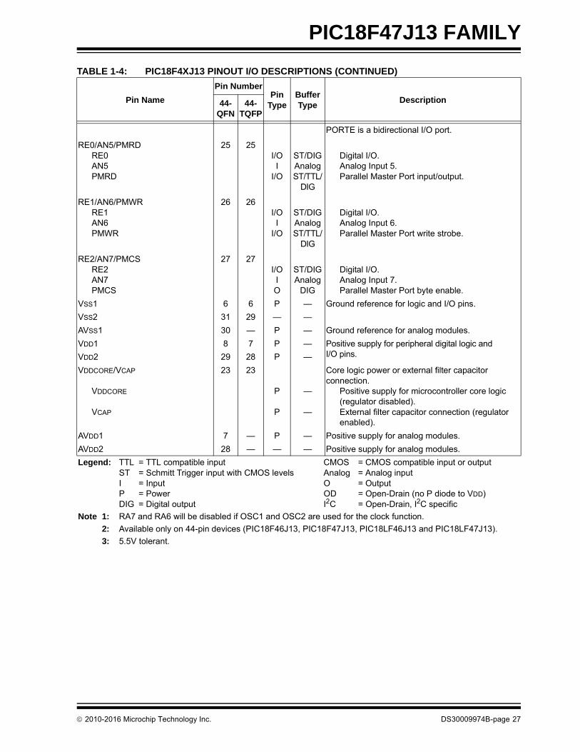
PIC18F47J13 FAMILY
PORTE is a bidirectional I/O port.
RE0/AN5/PMRDRE0AN5PMRD
25 25I/OI
I/O
ST/DIGAnalogST/TTL/
DIG
Digital I/O.Analog Input 5.Parallel Master Port input/output.
RE1/AN6/PMWRRE1AN6PMWR
26 26I/OI
I/O
ST/DIGAnalogST/TTL/
DIG
Digital I/O.Analog Input 6.Parallel Master Port write strobe.
RE2/AN7/PMCSRE2AN7PMCS
27 27I/OIO
ST/DIGAnalog
DIG
Digital I/O.Analog Input 7.Parallel Master Port byte enable.
VSS1 6 6 P — Ground reference for logic and I/O pins.
VSS2 31 29 — —
AVSS1 30 — P — Ground reference for analog modules.
VDD1 8 7 P — Positive supply for peripheral digital logic and I/O pins.VDD2 29 28 P —
VDDCORE/VCAP
VDDCORE
VCAP
23 23
P
P
—
—
Core logic power or external filter capacitor connection.
Positive supply for microcontroller core logic (regulator disabled).External filter capacitor connection (regulatorenabled).
AVDD1 7 — P — Positive supply for analog modules.
AVDD2 28 — — — Positive supply for analog modules.
TABLE 1-4: PIC18F4XJ13 PINOUT I/O DESCRIPTIONS (CONTINUED)
Pin Name
Pin NumberPin
TypeBufferType
Description44-QFN
44-TQFP
Legend: TTL = TTL compatible input CMOS = CMOS compatible input or output ST = Schmitt Trigger input with CMOS levels Analog = Analog input I = Input O = Output P = Power OD = Open-Drain (no P diode to VDD)DIG = Digital output I2C = Open-Drain, I2C specific
Note 1: RA7 and RA6 will be disabled if OSC1 and OSC2 are used for the clock function.
2: Available only on 44-pin devices (PIC18F46J13, PIC18F47J13, PIC18LF46J13 and PIC18LF47J13).
3: 5.5V tolerant.

PIC18F47J13 FAMILY
DS30009974B-page 28 2010-2016 Microchip Technology Inc.
2.0 GUIDELINES FOR GETTING STARTED WITH PIC18FJ MICROCONTROLLERS
2.1 Basic Connection Requirements
Getting started with the PIC18F47J13 Family of 8-bitmicrocontrollers requires attention to a minimal set ofdevice pin connections before proceeding withdevelopment.
The following pins must always be connected:
• All VDD and VSS pins (see Section 2.2 “Power Supply Pins”)
• All AVDD and AVSS pins, regardless of whether or not the analog device features are used (see Section 2.2 “Power Supply Pins”)
• MCLR pin (see Section 2.3 “Master Clear (MCLR) Pin”)
• VCAP/VDDCORE pins (see Section 2.4 “Voltage Regulator Pins (VCAP/VDDCORE)”)
These pins must also be connected if they are beingused in the end application:
• PGC/PGD pins used for In-Circuit Serial Programming™ (ICSP™) and debugging purposes (see Section 2.5 “ICSP Pins”)
• OSCI and OSCO pins when an external oscillator source is used (see Section 2.6 “External Oscillator Pins”)
Additionally, the following pins may be required:
• VREF+/VREF- pins are used when external voltage reference for analog modules is implemented
The minimum mandatory connections are shown inFigure 2-1.
FIGURE 2-1: RECOMMENDED MINIMUM CONNECTIONS
Note: On 44-pin QFN packages, the AVDD andAVSS pins must always be connected,regardless of whether any of the analogmodules are being used. On other pack-age types, the AVDD and AVSS pins areinternally connected to the VDD/VSS pins.
PIC18FXXJXX
VD
D
VS
S
VDD
VSS
VSS
VDD
AV
DD
AV
SS
VD
D
VS
S
C1
R1
VDD
MCLRVCAP/VDDCORE
R2
C7
C2(2)
C3(2)
C4(2)C5(2)
C6(2)
Key (all values are recommendations):
C1 through C6: 0.1 F, 20V ceramic
C7: 10 F, 6.3V or greater, tantalum or ceramic
R1: 10 kΩ
R2: 100Ω to 470Ω
Note 1: See Section 2.4 “Voltage Regulator Pins (VCAP/VDDCORE)” for explanation of VCAP/VDDCORE connections.
2: The example shown is for a PIC18F device with five VDD/VSS and AVDD/AVSS pairs. Other devices may have more or less pairs; adjust the number of decoupling capacitors appropriately.
(1)

2010-2016 Microchip Technology Inc. DS30009974B-page 29
PIC18F47J13 FAMILY
2.2 Power Supply Pins
2.2.1 DECOUPLING CAPACITORS
The use of decoupling capacitors on every pair ofpower supply pins, such as VDD, VSS, AVDD andAVSS, is required.
Consider the following criteria when using decouplingcapacitors:
• Value and type of capacitor: A 0.1 F (100 nF), 10-20V capacitor is recommended. The capacitor should be a low-ESR device, with a resonance frequency in the range of 200 MHz and higher. Ceramic capacitors are recommended.
• Placement on the printed circuit board: The decoupling capacitors should be placed as close to the pins as possible. It is recommended to place the capacitors on the same side of the board as the device. If space is constricted, the capacitor can be placed on another layer on the PCB using a via; however, ensure that the trace length from the pin to the capacitor is no greater than 0.25 inch (6 mm).
• Handling high-frequency noise: If the board is experiencing high-frequency noise (upward of tens of MHz), add a second ceramic type capaci-tor in parallel to the above described decoupling capacitor. The value of the second capacitor can be in the range of 0.01 F to 0.001 F. Place this second capacitor next to each primary decoupling capacitor. In high-speed circuit designs, consider implementing a decade pair of capacitances as close to the power and ground pins as possible (e.g., 0.1 F in parallel with 0.001 F).
• Maximizing performance: On the board layout from the power supply circuit, run the power and return traces to the decoupling capacitors first, and then to the device pins. This ensures that the decoupling capacitors are first in the power chain. Equally important is to keep the trace length between the capacitor and the power pins to a minimum, thereby reducing PCB trace inductance.
2.2.2 TANK CAPACITORS
On boards with power traces running longer thansix inches in length, it is suggested to use a tank capac-itor for integrated circuits, including microcontrollers, tosupply a local power source. The value of the tankcapacitor should be determined based on the traceresistance that connects the power supply source tothe device, and the maximum current drawn by thedevice in the application. In other words, select the tankcapacitor so that it meets the acceptable voltage sag atthe device. Typical values range from 4.7 F to 47 F.
2.3 Master Clear (MCLR) Pin
The MCLR pin provides two specific devicefunctions: Device Reset, and Device Programmingand Debugging. If programming and debugging arenot required in the end application, a directconnection to VDD may be all that is required. Theaddition of other components, to help increase theapplication’s resistance to spurious Resets fromvoltage sags, may be beneficial. A typicalconfiguration is shown in Figure 2-1. Other circuitdesigns may be implemented, depending on theapplication’s requirements.
During programming and debugging, the resistanceand capacitance that can be added to the pin mustbe considered. Device programmers and debuggersdrive the MCLR pin. Consequently, specific voltagelevels (VIH and VIL) and fast signal transitions mustnot be adversely affected. Therefore, specific valuesof R1 and C1 will need to be adjusted based on theapplication and PCB requirements. For example, it isrecommended that the capacitor, C1, be isolatedfrom the MCLR pin during programming anddebugging operations by using a jumper (Figure 2-2).The jumper is replaced for normal run-timeoperations.
Any components associated with the MCLR pinshould be placed within 0.25 inch (6 mm) of the pin.
FIGURE 2-2: EXAMPLE OF MCLR PIN CONNECTIONS
Note 1: R1 10 k is recommended. A suggestedstarting value is 10 k. Ensure that theMCLR pin VIH and VIL specifications are met.
2: R2 470 will limit any current flowing intoMCLR from the external capacitor, C, in theevent of MCLR pin breakdown, due toElectrostatic Discharge (ESD) or ElectricalOverstress (EOS). Ensure that the MCLR pinVIH and VIL specifications are met.
C1
R2R1
VDD
MCLR
PIC18FXXJXXJP

PIC18F47J13 FAMILY
DS30009974B-page 30 2010-2016 Microchip Technology Inc.
2.4 Voltage Regulator Pins (VCAP/VDDCORE)
On “F” devices, a low-ESR (< 5Ω) capacitor is requiredon the VCAP/VDDCORE pin to stabilize the voltageregulator output voltage. The VCAP/VDDCORE pin mustnot be connected to VDD and must use a capacitor of 10F connected to ground. The type can be ceramic ortantalum. A suitable example is the MurataGRM21BF50J106ZE01 (10 F, 6.3V) or equivalent.Designers may use Figure 2-3 to evaluate ESRequivalence of candidate devices.
It is recommended that the trace length not exceed0.25 inch (6 mm). Refer to Section 30.0 “ElectricalCharacteristics” for additional information.
On “LF” devices, the VCAP/VDDCORE pin must be tied toa voltage supply at the VDDCORE level. Refer toSection 30.0 “Electrical Characteristics” forinformation on VDD and VDDCORE.
Note that the “LF” versions of these devices areprovided with the voltage regulator permanentlydisabled; they must always be provided with a supplyvoltage on the VDDCORE pin.
FIGURE 2-3: FREQUENCY vs. ESR PERFORMANCE FOR SUGGESTED VCAP
2.5 ICSP Pins
The PGC and PGD pins are used for In-Circuit SerialProgramming™ (ICSP™) and debugging purposes. Itis recommended to keep the trace length between theICSP connector and the ICSP pins on the device asshort as possible. If the ICSP connector is expected toexperience an ESD event, a series resistor is recom-mended, with the value in the range of a few tens ofohms, not to exceed 100Ω.
Pull-up resistors, series diodes, and capacitors on thePGC and PGD pins are not recommended as they willinterfere with the programmer/debugger communica-tions to the device. If such discrete components are anapplication requirement, they should be removed fromthe circuit during programming and debugging. Alter-natively, refer to the AC/DC characteristics and timingrequirements information in the respective deviceFlash programming specification for information oncapacitive loading limits, and pin input voltage high(VIH) and input low (VIL) requirements.
For device emulation, ensure that the “CommunicationChannel Select” (i.e., PGCx/PGDx pins) programmedinto the device matches the physical connections forthe ICSP to the Microchip debugger/emulator tool.
For more information on available Microchipdevelopment tools connection requirements, refer toSection 29.0 “Development Support”.
10
1
0.1
0.01
0.0010.01 0.1 1 10 100 1000 10,000
Frequency (MHz)
ES
R (
)
Note: Data for Murata GRM21BF50J106ZE01 shown.Measurements at 25°C, 0V DC bias.

2010-2016 Microchip Technology Inc. DS30009974B-page 31
PIC18F47J13 FAMILY
2.6 External Oscillator Pins
Many microcontrollers have options for at least twooscillators: a high-frequency primary oscillator and alow-frequency secondary oscillator (refer toSection 3.0 “Oscillator Configurations” for details).
The oscillator circuit should be placed on the sameside of the board as the device. Place the oscillatorcircuit close to the respective oscillator pins with nomore than 0.5 inch (12 mm) between the circuitcomponents and the pins. The load capacitors shouldbe placed next to the oscillator itself, on the same sideof the board.
Use a grounded copper pour around the oscillator cir-cuit to isolate it from surrounding circuits. Thegrounded copper pour should be routed directly to theMCU ground. Do not run any signal traces or powertraces inside the ground pour. Also, if using a two-sidedboard, avoid any traces on the other side of the boardwhere the crystal is placed.
Layout suggestions are shown in Figure 2-4. In-linepackages may be handled with a single-sided layoutthat completely encompasses the oscillator pins. Withfine-pitch packages, it is not always possible to com-pletely surround the pins and components. A suitablesolution is to tie the broken guard sections to a mirroredground layer. In all cases, the guard trace(s) must bereturned to ground.
In planning the application’s routing and I/O assign-ments, ensure that adjacent port pins and other signalsin close proximity to the oscillator are benign (i.e., freeof high frequencies, short rise and fall times, and othersimilar noise).
For additional information and design guidance onoscillator circuits, please refer to these MicrochipApplication Notes, available at the corporate website(www.microchip.com):
• AN826, Crystal Oscillator Basics and Crystal Selection for rfPIC™ and PICmicro® Devices
• AN849, Basic PICmicro® Oscillator Design
• AN943, Practical PICmicro® Oscillator Analysis and Design
• AN949, Making Your Oscillator Work
2.7 Unused I/Os
Unused I/O pins should be configured as outputs anddriven to a logic low state. Alternatively, connect a 1 kΩto 10 kΩ resistor to VSS on unused pins and drive theoutput to logic low.
FIGURE 2-4: SUGGESTED PLACEMENT OF THE OSCILLATOR CIRCUIT
GND
`
`
`
OSC1
OSC2
T1OSO
T1OS I
Copper Pour Primary OscillatorCrystal
Timer1 OscillatorCrystal
DEVICE PINS
PrimaryOscillator
C1
C2
T1 Oscillator: C1 T1 Oscillator: C2
(tied to ground)
Single-Sided and In-Line Layouts:
Fine-Pitch (Dual-Sided) Layouts:
GND
OSCO
OSCI
Bottom LayerCopper Pour
OscillatorCrystal
Top Layer Copper Pour
C2
C1
DEVICE PINS
(tied to ground)
(tied to ground)

PIC18F47J13 FAMILY
DS30009974B-page 32 2010-2016 Microchip Technology Inc.
3.0 OSCILLATOR CONFIGURATIONS
3.1 Overview
Devices in the PIC18F47J13 Family incorporate adifferent oscillator and microcontroller clock systemthan general purpose PIC18F devices.
The PIC18F47J13 Family has additional prescalers andpostscalers, which have been added to accommodate awide range of oscillator frequencies. The PIC18F47J13provides two PLL circuits: a 4x multiplier PLL and a96 MHz PLL enabling 48 MHz operation from the 8 MHzinternal oscillator. Figure 3-1 provides an overview of theoscillator structure.
Other oscillator features used in PIC18 enhancedmicrocontrollers, such as the internal oscillator blockand clock switching, remain the same. They arediscussed later in this chapter.
3.1.1 OSCILLATOR CONTROL
The operation of the oscillator in PIC18F47J13 Familydevices is controlled through three Configuration regis-ters and two control registers. Configuration registers,CONFIG1L, CONFIG1H and CONFIG2L, select theoscillator mode, PLL prescaler and CPU divideroptions. As Configuration bits, these are set when thedevice is programmed and left in that configuration untilthe device is reprogrammed.
The OSCCON register (Register 3-2) selects the ActiveClock mode. It is primarily used in controlling clockswitching in power-managed modes. Its use isdiscussed in Section 3.3.1 “Oscillator ControlRegister”.
The OSCTUNE register (Register 3-1) is used to trim theINTOSC frequency source and select the low-frequencyclock source that drives several special features. TheOSCTUNE register is also used to activate or disable thePhase Locked Loop (PLL). Its use is described inSection 3.2.5.1 “OSCTUNE Register”.
3.2 Oscillator Types
PIC18F47J13 Family devices can be operated in eightdistinct oscillator modes. Users can program theFOSC<2:0> Configuration bits to select one of themodes listed in Table 3-1. For oscillator modes whichproduce a clock output (CLKO) on pin, RA6, the outputfrequency will be one fourth of the peripheral clockfrequency. The clock output stops when in Sleep mode,but will continue during Idle mode (see Figure 3-1).
3.2.1 OSCILLATOR MODES
A network of MUXes, clock dividers and two PLLcircuits have been provided, which can be used toderive various microcontroller frequencies. Figure 3-1helps in understanding the oscillator structure of thePIC18F47J13 Family of devices.
TABLE 3-1: OSCILLATOR MODES
Mode Description
ECPLL External Clock Input mode, the PLL can be enabled or disabled in software, CLKO on RA6, apply external clock signal to RA7.
EC External Clock Input mode, the PLL is always disabled, CLKO on RA6, apply external clock signal to RA7.
HSPLL High-Speed Crystal/Resonator mode, PLL can be enabled or disabled in software, crystal/resonator connected between RA6 and RA7.
HS High-Speed Crystal/Resonator mode, PLL always disabled, crystal/resonator connected between RA6 and RA7.
INTOSCPLLO Internal Oscillator mode, PLL can be enabled or disabled in software, CLKO on RA6, port function on RA7, the internal oscillator block is used to derive both the primary clock source and the postscaled internal clock.
INTOSCPLL Internal Oscillator mode, PLL can be enabled or disabled in software, port function on RA6 and RA7, the internal oscillator block is used to derive both the primary clock source and the postscaled internal clock.
INTOSCO Internal Oscillator mode, PLL is always disabled, CLKO on RA6, port function on RA7, the output of the INTOSC postscaler serves as both the postscaled internal clock and the primary clock source.
INTOSC Internal Oscillator mode, PLL is always disabled, port function on RA6 and RA7, the output of the INTOSC postscaler serves as both the postscaled internal clock and the primary clock source.

2010-2016 Microchip Technology Inc. DS30009974B-page 33
PIC18F47J13 FAMILY
FIGURE 3-1: PIC18F47J13 FAMILY CLOCK DIAGRAM
OSC1
OSC2
Primary Oscillator
CPU
Peripherals
IDLE
INT
OS
C P
ost
scal
er
8 MHz
4 MHz
2 MHz
1 MHz
500 kHz
125 kHz
250 kHz
111
110
101
100
011
010
001
00031 kHz
INTRC31 kHz
InternalOscillator
Block
8 MHz8 MHz
01
OSCTUNE<7>
PLLDIV<2:0>
4 MHz
WDT, PWRT, FSCMand Two-Speed Start-up
OSCCON<6:4>
PLLEN
1
0
FOSC<2>
1
0
PL
L P
resc
ale
r
96 MHzPLL(1) 2
00
FOSC<2:1>
Oth
er
00
01
OSCCON<1:0>
11 4
RA6
CLKOEnabled Modes
Timer1 Clock(3)
PostscaledInternal Clock
T1OSI
T1OSO
Secondary Oscillator
Note 1: The 96 MHz PLL requires a 4 MHz input and it produces a 96 MHz output. The 96 MHz PLL prescaler enables source clocks of 4, 8, 12, 16, 20, 24, 40 or 48 MHz to provide the 4 MHz input.
2: The 4x PLL requires an input clock source between 4 and 12 MHz. When using INTOSC to provide the 4x PLL input, the INTOSC postscaler must be set to either 8 MHz or 4 MHz. Selecting other INTOSC postscaler settings will operate the PLL outside of the specification.
3: Selecting the Timer1 clock or postscaled internal clock will turn off the primary oscillator (unless required by the reference clock of Section 3.4 “Reference Clock Output”) and PLL.
12 10 6 5 4 3 2 1
000001010011100101110111
48 MHz
Primary ClockSource
CFGPLLEN1
0
0
1
4x PLL(2)
PLLSEL
FOSC<2>

PIC18F47J13 FAMILY
DS30009974B-page 34 2010-2016 Microchip Technology Inc.
3.2.2 CRYSTAL OSCILLATOR/CERAMIC RESONATORS
In HS and HSPLL Oscillator modes, a crystal orceramic resonator is connected to the OSC1 andOSC2 pins to establish oscillation. Figure 3-2 displaysthe pin connections.
The oscillator design requires the use of a parallelresonant crystal.
FIGURE 3-2: CRYSTAL/CERAMIC RESONATOR OPERATION (HS OR HSPLL CONFIGURATION)
TABLE 3-2: CAPACITOR SELECTION FOR CERAMIC RESONATORS
TABLE 3-3: CAPACITOR SELECTION FOR CRYSTAL OSCILLATOR
An internal postscaler allows users to select a clockfrequency other than that of the crystal or resonator.Frequency division is determined by the CPDIVConfiguration bits. Users may select a clock frequencyof the oscillator frequency, or 1/2, 1/3 or 1/6 of thefrequency.
Note: Use of a series resonant crystal may givea frequency out of the crystalmanufacturer’s specifications.
Typical Capacitor Values Used:
Mode Freq OSC1 OSC2
HS 8.0 MHz16.0 MHz
27 pF22 pF
27 pF22 pF
Capacitor values are for design guidance only.
These capacitors were tested with the resonatorslisted below for basic start-up and operation. Thesevalues are not optimized.
Different capacitor values may be required to produceacceptable oscillator operation. The user should testthe performance of the oscillator over the expectedVDD and temperature range for the application.
See the notes following Table 3-3 for additionalinformation.
Resonators Used:
4.0 MHz
8.0 MHz
16.0 MHz
Note 1: See Table 3-2 and Table 3-3 for initial values of C1 and C2.
2: RS may be required to avoid overdriving crystals with low drive level specifications.
C1(1)
C2(1)
XTAL
OSC2
OSC1
Sleep
To
Logic
RS(2)
Internal
PIC18F47J13
Osc TypeCrystal
Freq
Typical Capacitor Values Tested:
C1 C2
HS 4 MHz 27 pF 27 pF
8 MHz 22 pF 22 pF
16 MHz 18 pF 18 pF
Capacitor values are for design guidance only.
These capacitors were tested with the crystals listedbelow for basic start-up and operation. These valuesare not optimized.
Different capacitor values may be required to produceacceptable oscillator operation. The user should testthe performance of the oscillator over the expectedVDD and temperature range for the application.
See the notes following this table for additionalinformation.
Crystals Used:
4 MHz
8 MHz
16 MHz
Note 1: Higher capacitance not only increasesthe stability of oscillator, but alsoincreases the start-up time.
2: Since each resonator/crystal has its owncharacteristics, the user should consultthe resonator/crystal manufacturer forappropriate values of externalcomponents.
3: Rs may be required to avoid overdrivingcrystals with low drive level specification.
4: Always verify oscillator performance overthe VDD and temperature range that isexpected for the application.

2010-2016 Microchip Technology Inc. DS30009974B-page 35
PIC18F47J13 FAMILY
3.2.3 EXTERNAL CLOCK INPUT
The EC and ECPLL Oscillator modes require anexternal clock source to be connected to the OSC1 pin.There is no oscillator start-up time required after aPower-on Reset (POR) or after an exit from Sleep mode.
In the EC Oscillator mode, the oscillator frequency,divided by 4, is available on the OSC2 pin. In theECPLL Oscillator mode, the PLL output, divided by 4,is available on the OSC2 pin. This signal may be usedfor test purposes or to synchronize other logic.Figure 3-3 displays the pin connections for the ECOscillator mode.
FIGURE 3-3: EXTERNAL CLOCK INPUT OPERATION (EC AND ECPLL CONFIGURATION)
3.2.4 PLL FREQUENCY MULTIPLIER
A Phase Locked Loop (PLL) circuit provides an option forusers who want to use a low-frequency oscillator circuitor clock the device up to its highest rated frequency froma crystal oscillator. This may be useful for customers whoare concerned with EMI due to high-frequency crystals orusers who require higher clock speeds from the internaloscillator. PIC18F47J13 Family devices include two PLLcircuits: a 4x PLL and a 96 MHz PLL.
Either PLL can be enabled in HSPLL, ECPLL,INTOSCPLL and INTOSCPLLO Oscillator modes bysetting the PLLEN bit (OSCTUNE<6>) or by clearingthe CFGPLLEN bit (CONFIG1L<4>).
The 96 MHz PLL is designed to produce a fixed96 MHz reference clock from a fixed 4 MHz input. Theoutput can then be divided and used for producing a48 MHz microcontroller core clock. Because the PLLhas a fixed frequency input and output, there are eightprescaling options to match the oscillator input fre-quency to the PLL. This prescaler allows the PLL to beused with crystals, resonators and external clocks,which are integer multiple frequencies of 4 MHz. Forexample, a 12 MHz crystal could be used in a prescalerDivide-by-Three mode to drive the 96 MHz PLL.
The 4x PLL is designed to produce variable referenceclocks of 16 to 48 MHz from any input clock between4 and 12 MHz. The PLLSEL (CONFIG3H<2>) Config-uration bit is used to select which PLL circuit will beused by the application.
3.2.5 INTERNAL OSCILLATOR BLOCK
The PIC18F47J13 Family devices include an internaloscillator block which generates two different clocksignals; either can be used as the microcontroller’sclock source. The internal oscillator may eliminate theneed for external oscillator circuits on the OSC1 and/orOSC2 pins.
The main output (INTOSC) is an 8 MHz clock sourcewhich can be used to directly drive the device clock. Italso drives the INTOSC postscaler which can provide arange of clock frequencies from 31 kHz to 8 MHz.Additionally, the INTOSC may be used in conjunctionwith a PLL to generate clock frequencies up to 48 MHz.
The other clock source is the internal RC oscillator(INTRC) which provides a nominal 31 kHz output.INTRC is enabled if it is selected as the device clocksource. It is also enabled automatically when any of thefollowing are enabled:
• Power-up Timer
• Fail-Safe Clock Monitor
• Watchdog Timer
• Two-Speed Start-up
These features are discussed in larger detail inSection 27.0 “Special Features of the CPU”.
The clock source frequency (INTOSC direct, INTRCdirect or INTOSC postscaler) is selected by configuringthe IRCF bits of the OSCCON register (page 39).
OSC1/CLKI
OSC2/CLKOFOSC/4
Clock fromExt. System PIC18F47J13

PIC18F47J13 FAMILY
DS30009974B-page 36 2010-2016 Microchip Technology Inc.
3.2.5.1 OSCTUNE Register
The internal oscillator’s output has been calibrated atthe factory but can be adjusted in the user’s applica-tion. This is done by writing to the OSCTUNE register(Register 3-1).
When the OSCTUNE register is modified, the INTOSCfrequency will begin shifting to the new frequency. TheINTOSC clock will typically stabilize within 1 s. Codeexecution continues during this shift. There is noindication that the shift has occurred.
The OSCTUNE register also contains the INTSRC bit.The INTSRC bit allows users to select which internaloscillator provides the clock source when the 31 kHzfrequency option is selected. This is covered in largerdetail in Section 3.3.1 “Oscillator Control Register”.
The PLLEN bit, contained in the OSCTUNE register,can be used to enable or disable the internal PLLwhen running in one of the PLL type oscillator modes(e.g., INTOSCPLL). Oscillator modes that do not con-tain “PLL” in their name cannot be used with the PLL.In these modes, the PLL is always disabled regardlessof the setting of the PLLEN bit.
When configured for one of the PLL enabled modes, set-ting the PLLEN bit does not immediately switch thedevice clock to the PLL output. The PLL requires up toelectrical parameter, trc, to start-up and lock, duringwhich time, the device continues to be clocked. Once thePLL output is ready, the microcontroller core willautomatically switch to the PLL derived frequency.
3.2.5.2 Internal Oscillator Output Frequency and Drift
The internal oscillator block is calibrated at the factoryto produce an INTOSC output frequency of 8.0 MHz.However, this frequency may drift as VDD or tempera-ture changes, which can affect the controller operationin a variety of ways.
The low-frequency INTRC oscillator operates inde-pendently of the INTOSC source. Any changes inINTOSC across voltage and temperature are not nec-essarily reflected by changes in INTRC and vice versa.
3.2.5.3 Compensating for INTOSC Drift
It is possible to adjust the INTOSC frequency bymodifying the value in the OSCTUNE register. This hasno effect on the INTRC clock source frequency.
Tuning the INTOSC source requires knowing when tomake the adjustment, in which direction it should bemade, and in some cases, how large a change isneeded. When using the EUSART, for example, anadjustment may be required when it begins to generateframing errors or receives data with errors while inAsynchronous mode. Framing errors indicate that thedevice clock frequency is too high; to adjust for this,decrement the value in OSCTUNE to reduce the clockfrequency. On the other hand, errors in data may sug-gest that the clock speed is too low; to compensate,increment OSCTUNE to increase the clock frequency.
It is also possible to verify device clock speed againsta reference clock. Two timers may be used: one timeris clocked by the peripheral clock, while the other isclocked by a fixed reference source, such as the Tim-er1 oscillator. Both timers are cleared, but the timerclocked by the reference generates interrupts. Whenan interrupt occurs, the internally clocked timer is readand both timers are cleared. If the internally clockedtimer value is greater than expected, then the internaloscillator block is running too fast. To adjust for this,decrement the OSCTUNE register.
Finally, an ECCP module can use free-running Timer1(or Timer3), clocked by the internal oscillator block andan external event with a known period (i.e., AC powerfrequency). The time of the first event is captured in theCCPRxH:CCPRxL registers and is recorded for uselater. When the second event causes a capture, thetime of the first event is subtracted from the time of thesecond event. Since the period of the external event isknown, the time difference between events can becalculated.
If the measured time is greater than the calculated time,the internal oscillator block is running too fast; tocompensate, decrement the OSCTUNE register. If themeasured time is less than the calculated time, the inter-nal oscillator block is running too slow; to compensate,increment the OSCTUNE register.

2010-2016 Microchip Technology Inc. DS30009974B-page 37
PIC18F47J13 FAMILY REGISTER 3-1: OSCTUNE: OSCILLATOR TUNING REGISTER (ACCESS F9Bh)
R/W-0 R/W-0 R/W-0 R/W-0 R/W-0 R/W-0 R/W-0 R/W-0
INTSRC PLLEN(1) TUN5 TUN4 TUN3 TUN2 TUN1 TUN0
bit 7 bit 0
Legend:
R = Readable bit W = Writable bit U = Unimplemented bit, read as ‘0’
-n = Value at POR ‘1’ = Bit is set ‘0’ = Bit is cleared x = Bit is unknown
bit 7 INTSRC: Internal Oscillator Low-Frequency Source Select bit
1 = 31.25 kHz device clock derived from 8 MHz INTOSC source (divide-by-256 enabled)0 = 31 kHz device clock derived directly from INTRC internal oscillator
bit 6 PLLEN: Frequency Multiplier Enable bit(1)
1 = PLL is enabled0 = PLL is disabled
bit 5-0 TUN<5:0>: Frequency Tuning bits
011111 = Maximum frequency011110•••000001000000 = Center frequency; oscillator module is running at the calibrated frequency111111•••100000 = Minimum frequency
Note 1: When the CFGPLLEN Configuration bit is used to enable the PLL, clearing OSCTUNE<6> will not disable the PLL.

PIC18F47J13 FAMILY
DS30009974B-page 38 2010-2016 Microchip Technology Inc.
3.3 Clock Sources and Oscillator Switching
Like previous PIC18 enhanced devices, thePIC18F47J13 Family includes a feature that allows thedevice clock source to be switched from the mainoscillator to an alternate, low-frequency clock source.PIC18F47J13 Family devices offer two alternate clocksources. When an alternate clock source is enabled,the various power-managed operating modes areavailable.
Essentially, there are three clock sources for thesedevices:
• Primary Oscillators
• Secondary Oscillators
• Internal Oscillator Block
The Primary Oscillators include the External Crystaland Resonator modes, the External Clock modes andthe internal oscillator block. The particular mode isdefined by the FOSC<2:0> Configuration bits. Thedetails of these modes are covered earlier in thischapter.
The Secondary Oscillators are external sources thatare not connected to the OSC1 or OSC2 pins. Thesesources may continue to operate even after thecontroller is placed in a power-managed mode.
PIC18F47J13 Family devices offer the Timer1 oscillatoras a secondary oscillator. This oscillator, in allpower-managed modes, is often the time base forfunctions such as a Real-Time Clock (RTC). Most often,a 32.768 kHz watch crystal is connected between theRC0/T1OSO/T1CKI/RP11 and RC1/CCP8/T1OSI/RP12pins. Like the HS Oscillator mode circuits, loadingcapacitors are also connected from each pin to ground.The Timer1 oscillator is discussed in larger detail inSection 13.5 “Timer1 Oscillator”.
In addition to being a primary clock source, thepostscaled internal clock is available as apower-managed mode clock source. The INTRCsource is also used as the clock source for severalspecial features, such as the WDT and Fail-Safe ClockMonitor (FSCM).
3.3.1 OSCILLATOR CONTROL REGISTER
The OSCCON register (Register 3-2) controls severalaspects of the device clock’s operation, both infull-power operation and in power-managed modes.
The System Clock Select bits, SCS<1:0>, select theclock source. The available clock sources are theprimary clock (defined by the FOSC<2:0> Configura-tion bits), the secondary clock (Timer1 oscillator) andthe postscaled internal clock.The clock source changesimmediately, after one or more of the bits is written to,following a brief clock transition interval. The SCS bitsare cleared on all forms of Reset.
The Internal Oscillator Frequency Select bits,IRCF<2:0>, select the frequency output provided on thepostscaled internal clock line. The choices are theINTRC source, the INTOSC source (8 MHz) or one ofthe frequencies derived from the INTOSC postscaler(31 kHz to 4 MHz). If the postscaled internal clock issupplying the device clock, changing the states of thesebits will have an immediate change on the internal oscil-lator’s output. On device Resets, the default outputfrequency of the INTOSC postscaler is set at 4 MHz.
When an output frequency of 31 kHz is selected(IRCF<2:0> = 000), users may choose the internaloscillator, which acts as the source. This is done withthe INTSRC bit in the OSCTUNE register(OSCTUNE<7>). Setting this bit selects INTOSC as a31.25 kHz clock source by enabling the divide-by-256output of the INTOSC postscaler. Clearing INTSRCselects INTRC (nominally 31 kHz) as the clock source.
This option allows users to select the tunable and moreprecise INTOSC as a clock source, while maintainingpower savings with a very low clock speed. Regardlessof the setting of INTSRC, INTRC always remains theclock source for features such as the WDT and theFSCM.
The OSTS and SOSCRUN bits indicate which clocksource is currently providing the device clock. The OSTSbit indicates that the Oscillator Start-up Timer (OST) hastimed out and the primary clock is providing the deviceclock in primary clock modes. The SOSCRUN bit (OSC-CON2<6>) indicates when the Timer1 oscillator isproviding the device clock in secondary clock modes. Inpower-managed modes, only one of these bits will be setat any time. If none of these bits are set, the INTRC isproviding the clock or the internal oscillator block has juststarted and is not yet stable.
The IDLEN bit determines if the device goes into Sleepmode, or one of the Idle modes, when the SLEEPinstruction is executed.

2010-2016 Microchip Technology Inc. DS30009974B-page 39
PIC18F47J13 FAMILY
The use of the flag and control bits in the OSCCONregister is discussed in more detail in Section 4.0“Low-Power Modes”.
3.3.2 OSCILLATOR TRANSITIONS
PIC18F47J13 Family devices contain circuitry toprevent clock “glitches” when switching between clocksources. A short pause in the device clock occursduring the clock switch. The length of this pause is thesum of two cycles of the old clock source and three tofour cycles of the new clock source. This formulaassumes that the new clock source is stable.
Clock transitions are discussed in more detail inSection 4.1.2 “Entering Power-Managed Modes”.
Note 1: The Timer1 crystal driver is enabled bysetting the T1OSCEN bit in the Timer1Control register (T1CON<3>). If the Tim-er1 oscillator is not enabled, then anyattempt to select the Timer1 clock sourcewill be ignored, unless the CONFIG2Lregister’s SOSCSEL<1:0> bits are set toDigital mode.
2: If Timer1 is driving a crystal, it is recom-mended that the Timer1 oscillator beoperating and stable prior to switching toit as the clock source; otherwise, a verylong delay may occur while the Timer1oscillator starts.
REGISTER 3-2: OSCCON: OSCILLATOR CONTROL REGISTER (ACCESS FD3h)
R/W-0 R/W-1 R/W-1 R/W-0 R-1(1) U-1 R/W-0 R/W-0
IDLEN IRCF2 IRCF1 IRCF0 OSTS — SCS1 SCS0
bit 7 bit 0
Legend:
R = Readable bit W = Writable bit U = Unimplemented bit
-n = Value at POR ‘1’ = Bit is set ‘0’ = Bit is cleared x = Bit is unknown
bit 7 IDLEN: Idle Enable bit1 = Device enters Idle mode on SLEEP instruction0 = Device enters Sleep mode on SLEEP instruction
bit 6-4 IRCF<2:0>: Internal Oscillator Frequency Select bitsWhen using INTOSC to drive the 4x PLL, select 8 MHz or 4 MHz only to avoid operating the 4x PLL outside of specification.
111 = 8 MHz (INTOSC drives clock directly)110 = 4 MHz(2)
101 = 2 MHz 100 = 1 MHz 011 = 500 kHz 010 = 250 kHz001 = 125 kHz000 = 31 kHz (from either INTOSC/256 or INTRC directly)(3)
bit 3 OSTS: Oscillator Start-up Time-out Status bit(1)
1 = Oscillator Start-up Timer time-out has expired; primary oscillator is running0 = Oscillator Start-up Timer time-out is running; primary oscillator is not ready
bit 2 Unimplemented: Read as ‘1’
bit 1-0 SCS<1:0>: System Clock Select bits11 = Postscaled internal clock (INTRC/INTOSC derived)10 = Reserved01 = Timer1 oscillator00 = Primary clock source (INTOSC postscaler output when FOSC<2:0> = 001 or 000)00 = Primary clock source (CPU divider output for other values of FOSC<2:0>)
Note 1: Reset value is ‘0’ when Two-Speed Start-up is enabled and ‘1’ if disabled.2: Default output frequency of INTOSC on Reset (4 MHz).3: Source selected by the INTSRC bit (OSCTUNE<7>).

PIC18F47J13 FAMILY
DS30009974B-page 40 2010-2016 Microchip Technology Inc.
REGISTER 3-3: OSCCON2: OSCILLATOR CONTROL REGISTER 2 (ACCESS F87h)
U-0 R-0(2) U-0 R/W-1 R/W-0(2) R/W-1 U-0 U-0
— SOSCRUN — SOSCDRV SOSCGO(3) — — —
bit 7 bit 0
Legend:
R = Readable bit W = Writable bit U = Unimplemented bit, read as ‘0’
-n = Value at POR ‘1’ = Bit is set ‘0’ = Bit is cleared x = Bit is unknown
bit 7 Unimplemented: Read as ‘0’
bit 6 SOSCRUN: SOSC Run Status bit
1 = System clock comes from secondary SOSC0 = System clock comes from an oscillator other than SOSC
bit 5 Unimplemented: Read as ‘0’
bit 4 SOSCDRV: SOSC Drive Control bit
1 = T1OSC/SOSC oscillator drive circuit is selected by Configuration bits, CONFIG2L<4:3>0 = Low-power T1OSC/SOSC circuit is selected
bit 3 SOSCGO: Oscillator Start Control bit(3)
1 = Turns on the oscillator, even if no peripherals are requesting it 0 = Oscillator is shut off unless peripherals are requesting it
bit 2 Reserved: Maintain as ‘1’
bit 1-0 Unimplemented: Read as ‘0’
Note 1: Reset value is ‘0’ when Two-Speed Start-up is enabled and ‘1’ if disabled.
2: Default output frequency of INTOSC on Reset (4 MHz).
3: When the SOSC is selected to run from a digital clock input, rather than an external crystal, this bit has no effect.

2010-2016 Microchip Technology Inc. DS30009974B-page 41
PIC18F47J13 FAMILY
3.4 Reference Clock Output
In addition to the peripheral clock/4 output in certainoscillator modes, the device clock in the PIC18F47J13Family can also be configured to provide a referenceclock output signal to a port pin. This feature is avail-able in all oscillator configurations and allows the userto select a greater range of clock submultiples to driveexternal devices in the application.
This reference clock output is controlled by theREFOCON register (Register 3-4). Setting the ROONbit (REFOCON<7>) makes the clock signal availableon the REFO (RB2) pin. The RODIV<3:0> bits enablethe selection of 16 different clock divider options.
The ROSSLP and ROSEL bits (REFOCON<5:4>)control the availability of the reference output duringSleep mode. The ROSEL bit determines if the oscillatoris on OSC1 and OSC2, or the current system clocksource is used for the reference clock output. TheROSSLP bit determines if the reference source isavailable on RB2 when the device is in Sleep mode.
To use the reference clock output in Sleep mode, boththe ROSSLP and ROSEL bits must be set. The deviceclock must also be configured for an EC or HS mode;otherwise, the oscillator on OSC1 and OSC2 will bepowered down when the device enters Sleep mode.Clearing the ROSEL bit allows the reference outputfrequency to change as the system clock changesduring any clock switches.
REGISTER 3-4: REFOCON: REFERENCE OSCILLATOR CONTROL REGISTER (BANKED F3Dh)
R/W-0 U-0 R/W-0 R/W-0 R/W-0 R/W-0 R/W-0 R/W-0
ROON — ROSSLP ROSEL RODIV3 RODIV2 RODIV1 RODIV0
bit 7 bit 0
Legend:
R = Readable bit W = Writable bit U = Unimplemented bit, read as ‘0’
-n = Value at POR ‘1’ = Bit is set ‘0’ = Bit is cleared x = Bit is unknown
bit 7 ROON: Reference Oscillator Output Enable bit
1 = Reference oscillator is enabled on REFO pin0 = Reference oscillator is disabled
bit 6 Unimplemented: Read as ‘0’
bit 5 ROSSLP: Reference Oscillator Output Stop in Sleep bit
1 = Reference oscillator continues to run in Sleep0 = Reference oscillator is disabled in Sleep
bit 4 ROSEL: Reference Oscillator Source Select bit
1 = Primary oscillator crystal/resonator is used as the base clock(1)
0 = System clock (FOSC) is used as the base clock; the base clock reflects any clock switching of the device
bit 3-0 RODIV<3:0>: Reference Oscillator Divisor Select bits
1111 = Base clock value divided by 32,7681110 = Base clock value divided by 16,3841101 = Base clock value divided by 8,1921100 = Base clock value divided by 4,0961011 = Base clock value divided by 2,0481010 = Base clock value divided by 1,0241001 = Base clock value divided by 5121000 = Base clock value divided by 2560111 = Base clock value divided by 1280110 = Base clock value divided by 640101 = Base clock value divided by 320100 = Base clock value divided by 160011 = Base clock value divided by 80010 = Base clock value divided by 40001 = Base clock value divided by 20000 = Base clock value
Note 1: The crystal oscillator must be enabled using the FOSC<2:0> bits; the crystal maintains the operation in Sleep mode.

PIC18F47J13 FAMILY
DS30009974B-page 42 2010-2016 Microchip Technology Inc.
3.5 Effects of Power-Managed Modes on Various Clock Sources
When the PRI_IDLE mode is selected, the designatedprimary oscillator continues to run without interruption.For all other power-managed modes, the oscillatorusing the OSC1 pin is disabled.
In secondary clock modes (SEC_RUN and SEC_I-DLE), the Timer1 oscillator is operating and providingthe device clock. The Timer1 oscillator may also run inall power-managed modes if required to clock Timer1,Timer3 or Timer5.
In internal oscillator modes (RC_RUN and RC_IDLE),the internal oscillator block provides the device clocksource. The 31 kHz INTRC output can be used directlyto provide the clock and may be enabled to supportvarious special features regardless of thepower-managed mode (see Section 27.2 “WatchdogTimer (WDT)”, Section 27.4 “Two-Speed Start-up”and Section 27.5 “Fail-Safe Clock Monitor” for moreinformation on WDT, FSCM and Two-Speed Start-up).The INTOSC output at 8 MHz may be used directly toclock the device or may be divided down by the posts-caler. The INTOSC output is disabled if the clock is pro-vided directly from the INTRC output.
If Sleep mode is selected, all clock sources which areno longer required are stopped. Since all the transistorswitching currents have been stopped, Sleep modeachieves the lowest current consumption of the device(only leakage currents) outside of Deep Sleep.
Enabling any on-chip feature that will operate duringSleep mode increases the current consumed duringSleep mode. The INTRC is required to support WDToperation. The Timer1 oscillator may be operating tosupport an RTC. Other features may be operating thatdo not require a device clock source (i.e., MSSP slave,PMP, INTx pins, etc.). Peripherals that may addsignificant current consumption are listed inSection 30.2 “DC Characteristics: Power-Down andSupply Current PIC18F47J13 Family (Industrial)”.
3.6 Power-up Delays
Power-up delays are controlled by two timers so that noexternal Reset circuitry is required for most applica-tions. The delays ensure that the device is kept inReset until the device power supply is stable undernormal circumstances and the primary clock is operat-ing and stable. For additional information on power-updelays, see Section 5.6 “Power-up Timer (PWRT)”.
The first timer is the Power-up Timer (PWRT), whichprovides a fixed delay on power-up (parameter 33,Table 30-14).
The second timer is the Oscillator Start-up Timer(OST), intended to keep the chip in Reset until thecrystal oscillator is stable (HS mode). The OST doesthis by counting 1024 oscillator cycles before allowingthe oscillator to clock the device.
There is a delay of interval, TCSD (parameter 38,Table 30-14), following POR, while the controllerbecomes ready to execute instructions. This delay runsconcurrently with any other delays. This may be the onlydelay that occurs when any of the internal oscillator orEC modes are used as the primary clock source.

2010-2016 Microchip Technology Inc. DS30009974B-page 43
PIC18F47J13 FAMILY
4.0 LOW-POWER MODES
The PIC18F47J13 Family devices can manage powerconsumption through clocking to the CPU and theperipherals. In general, reducing the clock frequencyand number of circuits being clocked reduces powerconsumption.
For managing power in an application, the primarymodes of operation are:
• Run Mode
• Idle Mode
• Sleep Mode
• Deep Sleep Mode
Additionally, there is an Ultra Low-Power Wake-up(ULPWU) mode for generating an interrupt-on-changeon RA0.
These modes define which portions of the device areclocked and at what speed.
• The Run and Idle modes can use any of the three available clock sources (primary, secondary or internal oscillator blocks).
• The Sleep mode does not use a clock source.
The ULPWU mode on RA0 allows a slow falling voltageto generate an interrupt-on-change on RA0 withoutexcess current consumption. See Section 4.7 “UltraLow-Power Wake-up”.
The power-managed modes include severalpower-saving features offered on previous PIC®
devices, such as clock switching, ULPWU and Sleepmode. In addition, the PIC18F47J13 Family deviceshave added a new power-managed Deep Sleep mode.
4.1 Selecting Power-Managed Modes
Selecting a power-managed mode requires thesedecisions:
• Will the CPU be clocked?
• If so, which clock source will be used?
The IDLEN bit (OSCCON<7>) controls CPU clockingand the SCS<1:0> bits (OSCCON<1:0>) select theclock source. The individual modes, bit settings, clocksources and affected modules are summarized inTable 4-1.
4.1.1 CLOCK SOURCES
The SCS<1:0> bits allow the selection of one of threeclock sources for power-managed modes. They are:
• Primary clock source – Defined by the FOSC<2:0> Configuration bits
• Timer1 clock – Provided by the secondary oscillator
• Postscaled internal clock – Derived from the internal oscillator block
4.1.2 ENTERING POWER-MANAGED MODES
Switching from one clock source to another begins byloading the OSCCON register. The SCS<1:0> bitsselect the clock source.
Changing these bits causes an immediate switch to thenew clock source, assuming that it is running. Theswitch also may be subject to clock transition delays.These delays are discussed in Section 4.1.3 “ClockTransitions and Status Indicators” and subsequentsections.
Entry to the power-managed Idle or Sleep modes istriggered by the execution of a SLEEP instruction. Theactual mode that results depends on the status of theIDLEN bit.
Depending on the current mode and the mode beingswitched to, a change to a power-managed mode doesnot always require setting all of these bits. Many transi-tions may be done by changing the oscillator selectbits, the IDLEN bit or the DSEN bit prior to issuing aSLEEP instruction.
If the IDLEN and DSEN bits are already configuredcorrectly, it may only be necessary to perform a SLEEPinstruction to switch to the desired mode.

PIC18F47J13 FAMILY
DS30009974B-page 44 2010-2016 Microchip Technology Inc.
TABLE 4-1: LOW-POWER MODES
4.1.3 CLOCK TRANSITIONS AND STATUS INDICATORS
The length of the transition between clock sources isthe sum of two cycles of the old clock source and threeto four cycles of the new clock source. This formulaassumes that the new clock source is stable.
Two bits indicate the current clock source and itsstatus: OSTS (OSCCON<3>) and SOSCRUN (OSC-CON2<6>). In general, only one of these bits will be setin a given power-managed mode. When the OSTS bitis set, the primary clock would be providing the deviceclock. When the SOSCRUN bit is set, the Timer1 oscil-lator would be providing the clock. If neither of thesebits is set, INTRC would be clocking the device.
4.1.4 MULTIPLE SLEEP COMMANDS
The power-managed mode that is invoked with theSLEEP instruction is determined by the setting of theIDLEN and DSEN bits at the time the instruction is exe-cuted. If another SLEEP instruction is executed, thedevice will enter the power-managed mode specifiedby IDLEN and DSEN at that time. If IDLEN or DSENhave changed, the device will enter the newpower-managed mode specified by the new setting.
ModeDSCONH<7> OSCCON<7,1:0> Module Clocking
Available Clock and Oscillator SourceDSEN(1) IDLEN(1) SCS<1:0> CPU Peripherals
Sleep 0 0 N/A Off Off Timer1 oscillator and/or RTCC may optionally be enabled
Deep Sleep(3)
1 0 N/A Powered off(2)
Powered off RTCC can run uninterrupted using the Timer1 or internal low-power RC oscillator
PRI_RUN 0 N/A 00 Clocked Clocked The normal, full-power execution mode; primary clock source (defined by FOSC<2:0>)
SEC_RUN 0 N/A 01 Clocked Clocked Secondary – Timer1 oscillator
RC_RUN 0 N/A 11 Clocked Clocked Postscaled internal clock
PRI_IDLE 0 1 00 Off Clocked Primary clock source (defined by FOSC<2:0>)
SEC_IDLE 0 1 01 Off Clocked Secondary – Timer1 oscillator
RC_IDLE 0 1 11 Off Clocked Postscaled internal clock
Note 1: IDLEN and DSEN reflect their values when the SLEEP instruction is executed.2: Deep Sleep turns off the internal core voltage regulator to power down core logic. See Section 4.6 “Deep Sleep
Mode” for more information.3: Deep Sleep mode is only available on “F” devices, not “LF” devices.
Note: Executing a SLEEP instruction does notnecessarily place the device into Sleepmode. It acts as the trigger to place thecontroller into either the Sleep or DeepSleep mode, or one of the Idle modes,depending on the setting of the IDLEN bit.

2010-2016 Microchip Technology Inc. DS30009974B-page 45
PIC18F47J13 FAMILY
4.2 Run Modes
In the Run modes, clocks to both the core andperipherals are active. The difference between thesemodes is the clock source.
4.2.1 PRI_RUN MODE
The PRI_RUN mode is the normal, full-power execu-tion mode of the microcontroller. This is also the defaultmode upon a device Reset unless Two-Speed Start-upis enabled (see Section 27.4 “Two-Speed Start-up”for details). In this mode, the OSTS bit is set (seeSection 3.3.1 “Oscillator Control Register”).
4.2.2 SEC_RUN MODE
The SEC_RUN mode is the compatible mode to the“clock switching” feature offered in other PIC18devices. In this mode, the CPU and peripherals areclocked from the Timer1 oscillator. This gives users theoption of low-power consumption while still using ahigh-accuracy clock source.
SEC_RUN mode is entered by setting the SCS<1:0>bits to ‘01’. The device clock source is switched to theTimer1 oscillator (see Figure 4-1), the primaryoscillator is shut down, the SOSCRUN bit (OSC-CON2<6>) is set and the OSTS bit is cleared.
On transitions from SEC_RUN mode to PRI_RUNmode, the peripherals and CPU continue to be clockedfrom the Timer1 oscillator while the primary clock isstarted. When the primary clock becomes ready, aclock switch back to the primary clock occurs (seeFigure 4-2). When the clock switch is complete, theSOSCRUN bit is cleared, the OSTS bit is set and theprimary clock would be providing the clock. The IDLENand SCS bits are not affected by the wake-up; theTimer1 oscillator continues to run.
FIGURE 4-1: TRANSITION TIMING FOR ENTRY TO SEC_RUN MODE
FIGURE 4-2: TRANSITION TIMING FROM SEC_RUN MODE TO PRI_RUN MODE (HSPLL)
Note: The Timer1 oscillator should already berunning prior to entering SEC_RUNmode. If the T1OSCEN bit is not set whenthe SCS<1:0> bits are set to ‘01’, entry toSEC_RUN mode will not occur. If theTimer1 oscillator is enabled, but not yetrunning, device clocks will be delayed untilthe oscillator has started. In such situa-tions, initial oscillator operation is far fromstable and unpredictable operation mayresult.
Q4Q3Q2
OSC1
Peripheral
Program
Q1
T1OSI
Q1
Counter
Clock
CPUClock
PC + 2PC
1 2 3 n-1 n
Clock Transition
Q4Q3Q2 Q1 Q3Q2
PC + 4
Q1 Q3 Q4
OSC1
Peripheral
Program PC
T1OSI
PLL Clock
Q1
PC + 4
Q2
Output
Q3 Q4 Q1
CPU Clock
PC + 2
Clock
Counter
Q2 Q2 Q3
Note 1: TOST = 1024 TOSC; TPLL = 2 ms (approx). These intervals are not shown to scale.
SCS<1:0> Bits Changed
TPLL(1)
1 2 n-1 n
Clock
OSTS Bit Set
Transition
TOST(1)

PIC18F47J13 FAMILY
DS30009974B-page 46 2010-2016 Microchip Technology Inc.
4.2.3 RC_RUN MODE
In RC_RUN mode, the CPU and peripherals areclocked from the internal oscillator; the primary clock isshut down. This mode provides the best power conser-vation of all the Run modes while still executing code.It works well for user applications, which are not highlytiming-sensitive or do not require high-speed clocks atall times.
This mode is entered by setting the SCS<1:0> bits(OSCCON<1:0>) to ‘11’. When the clock source isswitched to the internal oscillator block (seeFigure 4-3), the primary oscillator is shut down and theOSTS bit is cleared.
On transitions from RC_RUN mode to PRI_RUN mode,the device continues to be clocked from the INTOSCblock while the primary clock is started. When theprimary clock becomes ready, a clock switch to theprimary clock occurs (see Figure 4-4). When the clockswitch is complete, the OSTS bit is set and the primaryclock is providing the device clock. The IDLEN andSCS bits are not affected by the switch. The INTRCclock source will continue to run if either the WDT or theFSCM is enabled.
FIGURE 4-3: TRANSITION TIMING TO RC_RUN MODE
FIGURE 4-4: TRANSITION TIMING FROM RC_RUN MODE TO PRI_RUN MODE
Q4Q3Q2
OSC1
Peripheral
Program
Q1
INTRC
Q1
Counter
Clock
CPUClock
PC + 2PC
1 2 3 n-1 n
Clock Transition
Q4Q3Q2 Q1 Q3Q2
PC + 4
Q1 Q3 Q4
OSC1
Peripheral
Program PC
INTRC
PLL Clock
Q1
PC + 4
Q2
Output
Q3 Q4 Q1
CPU Clock
PC + 2
Clock
Counter
Q2 Q2 Q3
Note 1: TOST = 1024 TOSC; TPLL = 2 ms (approx). These intervals are not shown to scale.
SCS<1:0> Bits Changed
TPLL(1)
1 2 n-1 n
Clock
OSTS Bit Set
Transition
TOST(1)

2010-2016 Microchip Technology Inc. DS30009974B-page 47
PIC18F47J13 FAMILY
4.3 Sleep Mode
The power-managed Sleep mode is identical to thelegacy Sleep mode offered in all other PIC devices. It isentered by clearing the IDLEN bit (the default state ondevice Reset) and executing the SLEEP instruction.This shuts down the selected oscillator (Figure 4-5). Allclock source status bits are cleared.
Entering the Sleep mode from any other mode does notrequire a clock switch. This is because no clocks areneeded once the controller has entered Sleep mode. Ifthe WDT is selected, the INTRC source will continue tooperate. If the Timer1 oscillator is enabled, it will alsocontinue to run.
When a wake event occurs in Sleep mode (by interrupt,Reset or WDT time-out), the device will not be clockeduntil the clock source selected by the SCS<1:0> bitsbecomes ready (see Figure 4-6), or it will be clockedfrom the internal oscillator if either the Two-SpeedStart-up or the FSCM is enabled (see Section 27.0“Special Features of the CPU”). In either case, theOSTS bit is set when the primary clock is providing thedevice clocks. The IDLEN and SCS bits are notaffected by the wake-up.
FIGURE 4-5: TRANSITION TIMING FOR ENTRY TO SLEEP MODE
FIGURE 4-6: TRANSITION TIMING FOR WAKE FROM SLEEP (HSPLL)
Q4Q3Q2
OSC1
Peripheral
Sleep
Program
Q1Q1
Counter
Clock
CPUClock
PC + 2PC
Q3 Q4 Q1 Q2
OSC1
Peripheral
Program PC
PLL Clock
Q3 Q4
Output
CPU Clock
Q1 Q2 Q3 Q4 Q1 Q2
Clock
Counter PC + 6PC + 4
Q1 Q2 Q3 Q4
Wake Event
Note 1: TOST = 1024 TOSC; TPLL = 2 ms (approx). These intervals are not shown to scale.
TOST(1) TPLL(1)
OSTS Bit Set
PC + 2

PIC18F47J13 FAMILY
DS30009974B-page 48 2010-2016 Microchip Technology Inc.
4.4 Idle Modes
The Idle modes allow the controller’s CPU to beselectively shut down while the peripherals continue tooperate. Selecting a particular Idle mode allows usersto further manage power consumption.
If the IDLEN bit is set to ‘1’ when a SLEEP instruction isexecuted, the peripherals will be clocked from the clocksource selected using the SCS<1:0> bits; however, theCPU will not be clocked. The clock source status bits arenot affected. Setting IDLEN and executing a SLEEPinstruction provides a quick method of switching from agiven Run mode to its corresponding Idle mode.
If the WDT is selected, the INTRC source will continueto operate. If the Timer1 oscillator is enabled, it will alsocontinue to run.
Since the CPU is not executing instructions, the onlyexits from any of the Idle modes are by interrupt, WDTtime-out or a Reset. When a wake event occurs, CPUexecution is delayed by an interval of TCSD
(parameter 38, Table 30-14) while it becomes ready toexecute code. When the CPU begins executing code,it resumes with the same clock source for the currentIdle mode. For example, when waking from RC_IDLEmode, the internal oscillator block will clock the CPUand peripherals (in other words, RC_RUN mode). TheIDLEN and SCS bits are not affected by the wake-up.
While in any Idle or Sleep mode, a WDT time-out willresult in a WDT wake-up to the Run mode currentlyspecified by the SCS<1:0> bits.
4.4.1 PRI_IDLE MODE
This mode is unique among the three low-power Idlemodes, in that it does not disable the primary deviceclock. For timing-sensitive applications, this allows forthe fastest resumption of device operation with its moreaccurate primary clock source, since the clock sourcedoes not have to “warm up” or transition from anotheroscillator.
PRI_IDLE mode is entered from PRI_RUN mode bysetting the IDLEN bit and executing a SLEEP instruc-tion. If the device is in another Run mode, set IDLENfirst, then set the SCS bits to ‘00’ and execute SLEEP.Although the CPU is disabled, the peripherals continueto be clocked from the primary clock source specifiedby the FOSC<1:0> Configuration bits. The OSTS bitremains set (see Figure 4-7).
When a wake event occurs, the CPU is clocked from theprimary clock source. A delay of interval, TCSD, isrequired between the wake event and when codeexecution starts. This is required to allow the CPU tobecome ready to execute instructions. After thewake-up, the OSTS bit remains set. The IDLEN andSCS bits are not affected by the wake-up (seeFigure 4-8).
4.4.2 SEC_IDLE MODE
In SEC_IDLE mode, the CPU is disabled but theperipherals continue to be clocked from the Timer1oscillator. This mode is entered from SEC_RUN by set-ting the IDLEN bit and executing a SLEEP instruction. Ifthe device is in another Run mode, set IDLEN first, thenset SCS<1:0> to ‘01’ and execute SLEEP. When theclock source is switched to the Timer1 oscillator, theprimary oscillator is shut down, the OSTS bit is clearedand the SOSCRUN bit is set.
When a wake event occurs, the peripherals continue tobe clocked from the Timer1 oscillator. After an intervalof TCSD following the wake event, the CPU begins exe-cuting code being clocked by the Timer1 oscillator. TheIDLEN and SCS bits are not affected by the wake-up;the Timer1 oscillator continues to run (see Figure 4-8).
Note: The Timer1 oscillator should already berunning prior to entering SEC_IDLEmode. If the T1OSCEN bit is not set whenthe SLEEP instruction is executed, theSLEEP instruction will be ignored andentry to SEC_IDLE mode will not occur. Ifthe Timer1 oscillator is enabled, but notyet running, peripheral clocks will bedelayed until the oscillator has started. Insuch situations, initial oscillator operationis far from stable and unpredictable oper-ation may result.

2010-2016 Microchip Technology Inc. DS30009974B-page 49
PIC18F47J13 FAMILY
FIGURE 4-7: TRANSITION TIMING FOR ENTRY TO IDLE MODE
FIGURE 4-8: TRANSITION TIMING FOR WAKE FROM IDLE TO RUN MODE
Q1
Peripheral
Program PC PC + 2
OSC1
Q3 Q4 Q1
CPU Clock
Clock
Counter
Q2
OSC1
Peripheral
Program PC
CPU Clock
Q1 Q3 Q4
Clock
Counter
Q2
Wake Event
TCSD

PIC18F47J13 FAMILY
DS30009974B-page 50 2010-2016 Microchip Technology Inc.
4.4.3 RC_IDLE MODE
In RC_IDLE mode, the CPU is disabled but theperipherals continue to be clocked from the internaloscillator block. This mode allows for controllablepower conservation during Idle periods.
From RC_RUN, this mode is entered by setting theIDLEN bit and executing a SLEEP instruction. If thedevice is in another Run mode, first set IDLEN, thenclear the SCS bits and execute SLEEP. When the clocksource is switched to the INTOSC block, the primaryoscillator is shut down and the OSTS bit is cleared.
When a wake event occurs, the peripherals continue tobe clocked from the internal oscillator block. After adelay of TCSD, following the wake event, the CPUbegins executing code being clocked by the INTRC.The IDLEN and SCS bits are not affected by thewake-up. The INTRC source will continue to run ifeither the WDT or the FSCM is enabled.
4.5 Exiting Idle and Sleep Modes
An exit from Sleep mode, or any of the Idle modes, istriggered by an interrupt, a Reset or a WDT time-out.This section discusses the triggers that cause exitsfrom power-managed modes. The clocking subsystemactions are discussed in each of the power-managedmodes sections (see Section 4.2 “Run Modes”,Section 4.3 “Sleep Mode” and Section 4.4 “IdleModes”).
4.5.1 EXIT BY INTERRUPT
Any of the available interrupt sources can cause thedevice to exit from an Idle mode, or the Sleep mode, toa Run mode. To enable this functionality, an interruptsource must be enabled by setting its enable bit in oneof the INTCON or PIE registers. The exit sequence isinitiated when the corresponding interrupt flag bit is set.
On all exits from Idle or Sleep modes by interrupt, codeexecution branches to the interrupt vector if theGIE/GIEH bit (INTCON<7>) is set. Otherwise, codeexecution continues or resumes without branching(see Section 9.0 “Interrupts”).
A fixed delay of interval, TCSD, following the wakeevent, is required when leaving Sleep mode. This delayis required for the CPU to prepare for execution.Instruction execution resumes on the first clock cyclefollowing this delay.
4.5.2 EXIT BY WDT TIME-OUT
A WDT time-out will cause different actions dependingon which power-managed mode the device is, whenthe time-out occurs.
If the device is not executing code (all Idle modes andSleep mode), the time-out will result in an exit from thepower-managed mode (see Section 4.2 “RunModes” and Section 4.3 “Sleep Mode”). If the deviceis executing code (all Run modes), the time-out willresult in a WDT Reset (see Section 27.2 “WatchdogTimer (WDT)”).
The WDT and postscaler are cleared by one of thefollowing events:
• Executing a SLEEP or CLRWDT instruction
• The loss of a currently selected clock source (if the FSCM is enabled)
4.5.3 EXIT BY RESET
Exiting an Idle or Sleep mode by Reset automaticallyforces the device to run from the INTRC.

2010-2016 Microchip Technology Inc. DS30009974B-page 51
PIC18F47J13 FAMILY
4.5.4 EXIT WITHOUT AN OSCILLATOR START-UP DELAY
Certain exits from power-managed modes do notinvoke the OST at all. There are two cases:
• PRI_IDLE mode (where the primary clock source is not stopped) and the primary clock source is the EC mode
• PRI_IDLE mode and the primary clock source is the ECPLL mode
In these instances, the primary clock source eitherdoes not require an oscillator start-up delay, since it isalready running (PRI_IDLE), or normally does notrequire an oscillator start-up delay (EC). However, afixed delay of interval, TCSD, following the wake event,is still required when leaving Sleep and Idle modes toallow the CPU to prepare for execution. Instructionexecution resumes on the first clock cycle following thisdelay.
4.6 Deep Sleep Mode
Deep Sleep mode brings the device into its lowestpower consumption state without requiring the use ofexternal switches to remove power from the device.During Deep Sleep, the on-chip VDDCORE voltage reg-ulator is powered down, effectively disconnectingpower to the core logic of the microcontroller.
On devices that support it, the Deep Sleep mode isentered by:
• Setting the REGSLP (WDTCON<7>) bit
• Clearing the IDLEN bit
• Clearing the GIE bit
• Setting the DSEN bit (DSCONH<7>)
• Executing one single-cycle NOP instruction
• Executing the SLEEP instruction immediately after setting DSEN and the single NOP (no interrupts in between)
In order to minimize the possibility of inadvertently enter-ing Deep Sleep, the DSEN bit is cleared in hardwaretwo instruction cycles after having been set. Therefore,in order to enter Deep Sleep, the SLEEP instruction mustbe executed in the immediate instruction cycle after set-ting DSEN. If DSEN is not set when SLEEP is executed,the device will enter conventional Sleep mode instead.
During Deep Sleep, the core logic circuitry of themicrocontroller is powered down to reduce leakagecurrent. Therefore, most peripherals and functions ofthe microcontroller become unavailable during DeepSleep. However, a few specific peripherals and func-tions are powered directly from the VDD supply rail ofthe microcontroller, and therefore, can continue tofunction in Deep Sleep.
Entering Deep Sleep mode clears the DSWAKELregister. However, if the Real-Time Clock and Calendar(RTCC) is enabled prior to entering Deep Sleep, it willcontinue to operate uninterrupted.
The device has a dedicated Brown-out Reset (DSBOR)and Watchdog Timer Reset (DSWDT) for monitoringvoltage and time-out events in Deep Sleep. TheDSBOR and DSWDT are independent of the standardBOR and WDT used with other power-managed modes(Run, Idle and Sleep).
When a wake event occurs in Deep Sleep mode (byMCLR Reset, RTCC alarm, INT0 interrupt, ULPWU orDSWDT), the device will exit Deep Sleep mode andperform a Power-on Reset (POR). When the device isreleased from Reset, code execution will resume at thedevice’s Reset vector.
4.6.1 PREPARING FOR DEEP SLEEP
Because VDDCORE could fall below the SRAM retentionvoltage while in Deep Sleep mode, SRAM data couldbe lost in Deep Sleep. Exiting Deep Sleep modecauses a POR; as a result, most Special FunctionRegisters will reset to their default POR values.
Applications needing to save a small amount of datathroughout a Deep Sleep cycle can save the data to thegeneral purpose DSGPR0 and DSGPR1 registers. Thecontents of these registers are preserved while thedevice is in Deep Sleep, and will remain valid throughoutan entire Deep Sleep entry and wake-up sequence.
Note: Since Deep Sleep mode powers down themicrocontroller by turning off the on-chipVDDCORE voltage regulator, Deep Sleepcapability is available only on PIC18FXXJmembers in the device family. The on-chipvoltage regulator is not available inPIC18LFXXJ members of the devicefamily, and therefore, they do not supportDeep Sleep.

PIC18F47J13 FAMILY
DS30009974B-page 52 2010-2016 Microchip Technology Inc.
4.6.2 I/O PINS DURING DEEP SLEEP
During Deep Sleep, the general purpose I/O pins willretain their previous states.
Pins that are configured as inputs (TRISx bit set) priorto entry into Deep Sleep will remain high-impedanceduring Deep Sleep.
Pins that are configured as outputs (TRISx bit clear)prior to entry into Deep Sleep will remain as output pinsduring Deep Sleep. While in this mode, they will drivethe output level determined by their corresponding LATbit at the time of entry into Deep Sleep.
When the device wakes back up, the I/O pin behaviordepends on the type of wake up source.
If the device wakes back up by an RTCC alarm, INT0interrupt, DSWDT or ULPWU event, all I/O pins willcontinue to maintain their previous states, even after thedevice has finished the POR sequence and is executingapplication code again. Pins configured as inputs duringDeep Sleep will remain high-impedance, and pinsconfigured as outputs will continue to drive their previousvalue.
After waking up, the TRIS and LAT registers will bereset, but the I/O pins will still maintain their previousstates. If firmware modifies the TRIS and LAT valuesfor the I/O pins, they will not immediately go to thenewly configured states. Once the firmware clears theRELEASE bit (DSCONL<0>), the I/O pins will be“released”. This causes the I/O pins to take the statesconfigured by their respective TRIS and LAT bit values.
If the Deep Sleep BOR (DSBOR) circuit is enabled, andVDD drops below the DSBOR and VDD rail POR thresh-olds, the I/O pins will be immediately released similar toclearing the RELEASE bit. All previous state informa-tion will be lost, including the general purpose DSGPR0and DSGPR1 contents. See Section 4.6.5 “DeepSleep Brown-out Reset (DSBOR)” for additionaldetails regarding this scenario.
If a MCLR Reset event occurs during Deep Sleep, theI/O pins will also be released automatically, but in thiscase, the DSGPR0 and DSGPR1 contents will remainvalid.
In all other Deep Sleep wake-up cases, applicationfirmware needs to clear the RELEASE bit in order toreconfigure the I/O pins.
4.6.3 DEEP SLEEP WAKE-UP SOURCES
The device can be awakened from Deep Sleep mode bya MCLR, POR, RTCC, INT0 I/O pin interrupt, DSWDT orULPWU event. After waking, the device performs aPOR. When the device is released from Reset, codeexecution will begin at the device’s Reset vector.
The software can determine if the wake-up was causedfrom an exit from Deep Sleep mode by reading the DSbit (WDTCON<3>). If this bit is set, the POR wascaused by a Deep Sleep exit. The DS bit must bemanually cleared by the software.
The software can determine the wake event source byreading the DSWAKEH and DSWAKEL registers.When the application firmware is done using theDSWAKEH and DSWAKEL status registers, individualbits do not need to be manually cleared before enteringDeep Sleep again. When entering Deep Sleep mode,these registers are automatically cleared.
4.6.3.1 Wake-up Event Considerations
Deep Sleep wake-up events are only monitored whilethe processor is fully in Deep Sleep mode. If a wake-upevent occurs before Deep Sleep mode is entered, theevent status will not be reflected in the DSWAKEregisters. If the wake-up source asserts prior to enteringDeep Sleep, the CPU will either go to the interrupt vector(if the wake source has an interrupt bit and the interruptis fully enabled) or will abort the Deep Sleep entrysequence by executing past the SLEEP instruction, if theinterrupt was not enabled. In this case, a wake-up eventhandler should be placed after the SLEEP instruction toprocess the event and re-attempt entry into Deep Sleepif desired.
When the device is in Deep Sleep with more than onewake-up source simultaneously enabled, only the firstwake-up source to assert will be detected and loggedin the DSWAKEH/DSWAKEL status registers.
4.6.4 DEEP SLEEP WATCHDOG TIMER (DSWDT)
Deep Sleep has its own dedicated WDT (DSWDT) witha postscaler for time-outs of 2.1 ms to 25.7 days,configurable through the bits, DSWDTPS<3:0>.
The DSWDT can be clocked from either the INTRC orthe T1OSC/T1CKI input. If the T1OSC/T1CKI sourcewill be used with a crystal, the T1OSCEN bit in theT1CON register needs to be set prior to entering DeepSleep. The reference clock source is configured throughthe DSWDTOSC bit.
DSWDT is enabled through the DSWDTEN bit. EnteringDeep Sleep mode automatically clears the DSWDT. SeeSection 27.0 “Special Features of the CPU” for moreinformation.

2010-2016 Microchip Technology Inc. DS30009974B-page 53
PIC18F47J13 FAMILY
4.6.5 DEEP SLEEP BROWN-OUT RESET (DSBOR)
The Deep Sleep module contains a dedicated Deep SleepBOR (DSBOR) circuit. This circuit may be optionallyenabled through the DSBOREN Configuration bit.
The DSBOR circuit monitors the VDD supply railvoltage. The behavior of the DSBOR circuit isdescribed in Section 5.4 “Brown-out Reset (BOR)”.
4.6.6 RTCC PERIPHERAL AND DEEP SLEEP
The RTCC can operate uninterrupted during DeepSleep mode. It can wake the device from Deep Sleepby configuring an alarm.
The RTCC clock source is configured with theRTCOSC bit (CONFIG3L<1>). The available referenceclock sources are the INTRC and T1OSC/T1CKI. If theINTRC is used, the RTCC accuracy will directly dependon the INTRC tolerance. For more information onconfiguring the RTCC peripheral, see Section 17.0“Real-Time Clock and Calendar (RTCC)”.
4.6.7 TYPICAL DEEP SLEEP SEQUENCE
This section gives the typical sequence for using the DeepSleep mode. Optional steps are indicated and additionalinformation is given in notes at the end of the procedure.
1. Enable DSWDT (optional).(1)
2. Configure the DSWDT clock source (optional).(2)
3. Enable DSBOR (optional).(1)
4. Enable RTCC (optional).(3)
5. Configure the RTCC peripheral (optional).(3)
6. Configure the ULPWU peripheral (optional).(4)
7. Enable the INT0 Interrupt (optional).
8. Context save SRAM data by writing to theDSGPR0 and DSGPR1 registers (optional).
9. Set the REGSLP bit (WDTCON<7>) and clearthe IDLEN bit (OSCCON<7>).
10. If using an RTCC alarm for wake-up, wait untilthe RTCSYNC bit (RTCCFG<4>) is clear.
11. Enter Deep Sleep mode by setting the DSEN bit(DSCONH<7>), execute a NOP and issue aSLEEP instruction. The SLEEP instruction mustbe executed within 2 instruction cycles of settingthe DSEN bit.
12. Once a wake-up event occurs, the device willperform a POR Reset sequence. Code executionresumes at the device’s Reset vector.
13. Determine if the device exited Deep Sleep byreading the Deep Sleep bit, DS (WDTCON<3>).This bit will be set if there was an exit from DeepSleep mode.
14. Clear the Deep Sleep bit, DS (WDTCON<3>).
15. Determine the wake-up source by reading theDSWAKEH and DSWAKEL registers.
16. Determine if a DSBOR event occurred duringDeep Sleep mode by reading the DSBOR bit(DSCONL<1>).
17. Read the DSGPR0 and DSGPR1 context saveregisters (optional).
18. Clear the RELEASE bit (DSCONL<0>).
4.6.8 DEEP SLEEP FAULT DETECTION
If during Deep Sleep, the device is subjected tounusual operating conditions, such as an ElectrostaticDischarge (ESD) event, it is possible that internal cir-cuit states used by the Deep Sleep module couldbecome corrupted. If this were to happen, the devicemay exhibit unexpected behavior, such as a failure towake back up.
In order to prevent this type of scenario from occurring,the Deep Sleep module includes automaticself-monitoring capability. During Deep Sleep, criticalinternal nodes are continuously monitored in order todetect possible Fault conditions (which would notordinarily occur). If a Fault condition is detected, thecircuitry will set the DSFLT status bit (DSWAKEL<7>)and automatically wake the microcontroller from DeepSleep, causing a POR Reset.
During Deep Sleep, the Fault detection circuitry isalways enabled and does not require any specificconfiguration prior to entering Deep Sleep.
Note 1: DSWDT and DSBOR are enabledthrough the devices’ Configuration bits.For more information, see Section 27.1“Configuration Bits”.
2: The DSWDT and RTCC clock sourcesare selected through the devices’ Con-figuration bits. For more information, seeSection 27.1 “Configuration Bits”.
3: For more information, see Section 17.0“Real-Time Clock and Calendar(RTCC)”.
4: For more information on configuring thisperipheral, see Section 4.7 “UltraLow-Power Wake-up”.

PIC18F47J13 FAMILY
DS30009974B-page 54 2010-2016 Microchip Technology Inc.
4.6.9 DEEP SLEEP MODE REGISTERS
Deep Sleep mode registers are provided inRegister 4-1 through Register 4-6.
REGISTER 4-1: DSCONH: DEEP SLEEP CONTROL HIGH BYTE REGISTER (BANKED F4Dh)
R/W-0 U-0 U-0 U-0 U-0 R/W-0 R/W-0 R/W-0
DSEN(1) — — — — r DSULPEN RTCWDIS
bit 7 bit 0
Legend: r = Reserved bit
R = Readable bit W = Writable bit U = Unimplemented bit, read as ‘0’
-n = Value at POR ‘1’ = Bit is set ‘0’ = Bit is cleared x = Bit is unknown
bit 7 DSEN: Deep Sleep Enable bit(1)
1 = Deep Sleep mode is entered on a SLEEP command0 = Sleep mode is entered on a SLEEP command
bit 6-3 Unimplemented: Read as ‘0’
bit 2 Reserved: Maintain as ‘0’
bit 1 DSULPEN: Ultra Low-Power Wake-up Module Enable bit
1 = ULPWU module is enabled in Deep Sleep0 = ULPWU module is disabled in Deep Sleep
bit 0 RTCWDIS: RTCC Wake-up Disable bit
1 = Wake-up from RTCC is disabled0 = Wake-up from RTCC is enabled
Note 1: In order to enter Deep Sleep, Sleep must be executed within 2 instruction cycles after setting DSEN.
REGISTER 4-2: DSCONL: DEEP SLEEP LOW BYTE CONTROL REGISTER (BANKED F4Ch)
U-0 U-0 U-0 U-0 U-0 R/W-0 R/W-0(1) R/W-0(1)
— — — — — ULPWDIS DSBOR RELEASE
bit 7 bit 0
Legend:
R = Readable bit W = Writable bit U = Unimplemented bit, read as ‘0’
-n = Value at POR ‘1’ = Bit is set ‘0’ = Bit is cleared x = Bit is unknown
bit 7-3 Unimplemented: Read as ‘0’
bit 2 ULPWDIS: Ultra Low-Power Wake-up Disable bit
1 = ULPWU wake-up source is disabled0 = ULPWU wake-up source is enabled (must also set DSULPEN = 1)
bit 1 DSBOR: Deep Sleep BOR Event Status bit
1 = DSBOREN was enabled and VDD dropped below the DSBOR arming voltage during Deep Sleep,but did not fall below VDSBOR
0 = DSBOREN was disabled or VDD did not drop below the DSBOR arming voltage during DeepSleep
bit 0 RELEASE: I/O Pin State Release bit
Upon waking from Deep Sleep, the I/O pins maintain their previous states. Clearing this bit will release the I/O pins and allow their respective TRIS and LAT bits to control their states.
Note 1: This is the value when VDD is initially applied.

2010-2016 Microchip Technology Inc. DS30009974B-page 55
PIC18F47J13 FAMILY
REGISTER 4-3: DSGPR0: DEEP SLEEP PERSISTENT GENERAL PURPOSE REGISTER 0 (BANKED F4Eh)
R/W-xxxx(1)
Deep Sleep Persistent General Purpose bits
bit 7 bit 0
Legend:
R = Readable bit W = Writable bit U = Unimplemented bit, read as ‘0’
-n = Value at POR ‘1’ = Bit is set ‘0’ = Bit is cleared x = Bit is unknown
bit 7-0 Deep Sleep Persistent General Purpose bits
Contents are retained even in Deep Sleep mode.
Note 1: All register bits are maintained unless VDDCORE drops below the normal BOR threshold outside of Deep Sleep, or the device is in Deep Sleep and the dedicated DSBOR is enabled and VDD drops below the DSBOR threshold, or DSBOR is enabled or disabled, but VDD is hard cycled to near VSS.
REGISTER 4-4: DSGPR1: DEEP SLEEP PERSISTENT GENERAL PURPOSE REGISTER 1 (BANKED F4Fh)
R/W-xxxx(1)
Deep Sleep Persistent General Purpose bits
bit 7 bit 0
Legend:
R = Readable bit W = Writable bit U = Unimplemented bit, read as ‘0’
-n = Value at POR ‘1’ = Bit is set ‘0’ = Bit is cleared x = Bit is unknown
bit 7-0 Deep Sleep Persistent General Purpose bits
Contents are retained even in Deep Sleep mode.
Note 1: All register bits are maintained unless VDDCORE drops below the normal BOR threshold outside of Deep Sleep, or the device is in Deep Sleep and the dedicated DSBOR is enabled and VDD drops below the DSBOR threshold, or DSBOR is enabled or disabled, but VDD is hard cycled to near VSS.
REGISTER 4-5: DSWAKEH: DEEP SLEEP WAKE HIGH BYTE REGISTER (BANKED F4Bh)
U-0 U-0 U-0 U-0 U-0 U-0 U-0 R/W-0
— — — — — — — DSINT0
bit 7 bit 0
Legend:
R = Readable bit W = Writable bit U = Unimplemented bit, read as ‘0’
-n = Value at POR ‘1’ = Bit is set ‘0’ = Bit is cleared x = Bit is unknown
bit 7-1 Unimplemented: Read as ‘0’
bit 0 DSINT0: Interrupt-on-Change bit
1 = Interrupt-on-change was asserted during Deep Sleep0 = Interrupt-on-change was not asserted during Deep Sleep

PIC18F47J13 FAMILY
DS30009974B-page 56 2010-2016 Microchip Technology Inc.
REGISTER 4-6: DSWAKEL: DEEP SLEEP WAKE LOW BYTE REGISTER (BANKED F4Ah)
R/W-0 U-0 R/W-0 R/W-0 R/W-0 R/W-0 U-0 R/W-1
DSFLT — DSULP DSWDT DSRTC DSMCLR — DSPOR
bit 7 bit 0
Legend:
R = Readable bit W = Writable bit U = Unimplemented bit, read as ‘0’
-n = Value at POR ‘1’ = Bit is set ‘0’ = Bit is cleared x = Bit is unknown
bit 7 DSFLT: Deep Sleep Fault Detected bit
1 = A Deep Sleep Fault was detected during Deep Sleep0 = A Deep Sleep Fault was not detected during Deep Sleep
bit 6 Unimplemented: Read as ‘0’
bit 5 DSULP: Ultra Low-Power Wake-up Status bit
1 = An ultra low-power wake-up event occurred during Deep Sleep0 = An ultra low-power wake-up event did not occur during Deep Sleep
bit 4 DSWDT: Deep Sleep Watchdog Timer Time-out bit
1 = The Deep Sleep Watchdog Timer timed out during Deep Sleep0 = The Deep Sleep Watchdog Timer did not time out during Deep Sleep
bit 3 DSRTC: Real-Time Clock and Calendar Alarm bit
1 = The Real-Time Clock/Calendar triggered an alarm during Deep Sleep0 = The Real-Time Clock /Calendar did not trigger an alarm during Deep Sleep
bit 2 DSMCLR: MCLR Event bit
1 = The MCLR pin was asserted during Deep Sleep0 = The MCLR pin was not asserted during Deep Sleep
bit 1 Unimplemented: Read as ‘0’
bit 0 DSPOR: Power-on Reset Event bit
1 = The VDD supply POR circuit was active and a POR event was detected(1)
0 = The VDD supply POR circuit was not active, or was active, but did not detect a POR event
Note 1: Unlike the other bits in this register, this bit can be set outside of Deep Sleep.

2010-2016 Microchip Technology Inc. DS30009974B-page 57
PIC18F47J13 FAMILY
4.7 Ultra Low-Power Wake-up
The Ultra Low-Power Wake-up (ULPWU) on RA0 allowsa slow falling voltage to generate an interrupt-on-changewithout excess current consumption.
Follow these steps to use this feature:
1. Configure a remappable output pin to output theULPOUT signal.
2. Map an INTx interrupt-on-change input function tothe same pin as used for the ULPOUT output func-tion. Alternatively, in Step 1, configure ULPOUT tooutput onto a PORTB interrupt-on-change pin.
3. Charge the capacitor on RA0 by configuring theRA0 pin to an output and setting it to ‘1’.
4. Enable interrupt-on-change (PIE bit) for thecorresponding pin selected in Step 2.
5. Stop charging the capacitor by configuring RA0as an input.
6. Discharge the capacitor by setting the ULPENand ULPSINK bits in the WDTCON register.
7. Configure Sleep mode.
8. Enter Sleep mode.
When the voltage on RA0 drops below VIL, an interruptwill be generated, which will cause the device towake-up and execute the next instruction.
This feature provides a low-power technique forperiodically waking up the device from Sleep mode.The time-out is dependent on the discharge time of theRC circuit on RA0.
When the ULPWU module causes the device towake-up from Sleep mode, the ULPLVL (WDTCON<5>)bit is set. When the ULPWU module causes the deviceto wake-up from Deep Sleep, the DSULP(DSWAKEL<5>) bit is set. Software can check these bitsupon wake-up to determine the wake-up source. Also inSleep mode, only the remappable output function,ULPWU, will output this bit value to an RPn pin forexternally detecting wake-up events.
See Example 4-1 for initializing the ULPWU module.
Note: For module related bit definitions, see theWDTCON register in Section 27.2“Watchdog Timer (WDT)” and theDSWAKEL register (Register 4-6).

PIC18F47J13 FAMILY
DS30009974B-page 58 2010-2016 Microchip Technology Inc.
EXAMPLE 4-1: ULTRA LOW-POWER WAKE-UP INITIALIZATION
//*********************************************************************************//Configure a remappable output pin with interrupt capability//for ULPWU function (RP21 => RD4/INT1 in this example)//*********************************************************************************RPOR21 = 13;// ULPWU function mapped to RP21/RD4RPINR1 = 21;// INT1 mapped to RP21 (RD4)
//***************************//Charge the capacitor on RA0//***************************TRISAbits.TRISA0 = 0;PORTAbits.RA0 = 1;for(i = 0; i < 10000; i++) Nop();
//**********************************//Stop Charging the capacitor on RA0//**********************************TRISAbits.TRISA0 = 1;
//*****************************************//Enable the Ultra Low Power Wakeup module//and allow capacitor discharge//*****************************************WDTCONbits.ULPEN = 1;WDTCONbits.ULPSINK = 1;
//******************************************//Enable Interrupt for ULPW//******************************************//For Sleep//(assign the ULPOUT signal in the PPS module to a pin //which has also been assigned an interrupt capability, //such as INT1)INTCON3bits.INT1IF = 0;INTCON3bits.INT1IE = 1;
//********************//Configure Sleep Mode//********************//For SleepOSCCONbits.IDLEN = 0;
//For Deep SleepOSCCONbits.IDLEN = 0; // enable deep sleepDSCONHbits.DSEN = 1; // Note: must be set just before executing Sleep(); //****************//Enter Sleep Mode//****************Sleep();// for sleep, execution will resume here
// for deep sleep, execution will restart at reset vector (use WDTCONbits.DS to detect)

2010-2016 Microchip Technology Inc. DS30009974B-page 59
PIC18F47J13 FAMILY
A series resistor between RA0 and the externalcapacitor provides overcurrent protection for theRA0/AN0/C1INA/ULPWU/RP0 pin and can allow forsoftware calibration of the time-out (see Figure 4-9).
FIGURE 4-9: SERIAL RESISTOR
A timer can be used to measure the charge time anddischarge time of the capacitor. The charge time canthen be adjusted to provide the desired interrupt delay.This technique will compensate for the affects oftemperature, voltage and component accuracy. TheULPWU peripheral can also be configured as a simpleProgrammable Low-Voltage Detect (LVD) ortemperature sensor.
4.8 Peripheral Module Disable
All peripheral modules (except for I/O ports) also havea second control bit that can disable their functionality.These bits, known as the Peripheral Module Disable(PMD) bits, are generically named “xxxMD” (using“xxx” as the mnemonic version of the module’s name).
These bits are located in the PMDISx special functionregisters. In contrast to the module enable bits (gener-ically named “xxxEN” and located in bit position sevenof the control registers), the PMD bits must be set (= 1)to disable the modules.
While the PMD and module enable bits both disable aperipheral’s functionality, the PMD bit completely shutsdown the peripheral, effectively powering down allcircuits and removing all clock sources. This has theadditional effect of making any of the module’s controland buffer registers, mapped in the SFR space,unavailable for operations. Essentially, the peripheralceases to exist until the PMD bit is cleared.
This differs from using the module enable bit, whichallows the peripheral to be reconfigured and bufferregisters preloaded, even when the peripheral’soperations are disabled.
The PMD bits are most useful in highly power-sensitiveapplications. In these cases, the bits can be set beforethe main body of the application to remove peripheralsthat will not be needed at all.
Note: For more information, refer to AN879,Using the Microchip Ultra Low-PowerWake-up Module application note(DS00879).
R1
C1
RA0
TABLE 4-2: LOW-POWER MODE REGISTERS
Register Bit 7 Bit 6 Bit 5 Bit 4 Bit 3 Bit 2 Bit 1 Bit 0 Value on
POR, BOR
PMDIS3 CCP10MD CCP9MD CCP8MD CCP7MD CCP6MD CCP5MD CCP4MD — 0000 000–
PMDIS2 — TMR8MD — TMR6MD TMR5MD CMP3MD CMP2MD CMP1MD –0–0 0000
PMDIS1 PSPMD(1) CTMUMD RTCCMD(2) TMR4MD TMR3MD TMR2MD TMR1MD — 0000 000–
PMDIS0 ECCP3MD ECCP2MD ECCP1MD UART2MD UART1MD SPI2MD SP11MD ADCMD 0000 0000
Note 1: Not implemented on 28-pin devices (PIC18F26J13, PIC18F27J13, PIC18LF26J13 and PIC18LF27J13).2: To prevent accidental RTCC changes, the RTCCMD bit is normally locked. Use the following unlock sequence (with
interrupts disabled) to successfully modify the RTCCMD bit:
1. Write 55h to EECON2.
2. Write 0AAh to EECON2.
3. Immediately write the modified RTCCMD setting to PMDIS1.

PIC18F47J13 FAMILY
DS30009974B-page 60 2010-2016 Microchip Technology Inc.
5.0 RESETThe PIC18F47J13 Family of devices differentiatesamong various kinds of Reset:
a) Power-on Reset (POR)
b) MCLR Reset during normal operation
c) MCLR Reset during power-managed modes
d) Watchdog Timer (WDT) Reset (duringexecution)
e) Configuration Mismatch (CM)
f) Brown-out Reset (BOR)
g) RESET Instruction
h) Stack Full Reset
i) Stack Underflow Reset
j) Deep Sleep Reset
This section discusses Resets generated by MCLR,POR and BOR, and covers the operation of the variousstart-up timers.
For information on WDT Resets, see Section 27.2“Watchdog Timer (WDT)”. For Stack Reset events,see Section 6.1.4.4 “Stack Full and UnderflowResets” and for Deep Sleep mode, see Section 4.6“Deep Sleep Mode”.
Figure 5-1 provides a simplified block diagram of theon-chip Reset circuit.
5.1 RCON Register
Device Reset events are tracked through the RCONregister (Register 5-1). The lower five bits of the registerindicate that a specific Reset event has occurred. Inmost cases, these bits can only be set by the event andmust be cleared by the application after the event. Thestate of these flag bits, taken together, can be read toindicate the type of Reset that just occurred. This isdescribed in more detail in Section 5.7 “Reset State ofRegisters”.
The RCON register also has a control bit for settinginterrupt priority (IPEN). Interrupt priority is discussedin Section 9.0 “Interrupts”.
FIGURE 5-1: SIMPLIFIED BLOCK DIAGRAM OF ON-CHIP RESET CIRCUIT
External Reset
MCLR
VDD
WDTTime-out
VDD RiseDetect
PWRT
INTRC
POR Pulse
Chip_Reset
Brown-outReset(1)
RESET Instruction
StackPointer
Stack Full/Underflow Reset
Sleep
( )_IDLE
PWRT
S
R Q
Configuration Word Mismatch
Deep Sleep Reset
Note 1: The VDD monitoring BOR circuit can be enabled or disabled on “LF” devices based on the CONFIG3L<DSBOREN>Configuration bit. On “F” devices, the VDD monitoring BOR circuit is only enabled during Deep Sleep mode by CON-FIG3L<DSBOREN>.
2: The VDDCORE monitoring BOR circuit is only implemented on “F” devices. It is always used, except while in DeepSleep mode. The VDDCORE monitoring BOR circuit has a trip point threshold of VBOR (parameter D005).
VDDCORE
Brown-outReset(2)
LF: 11-Bit Ripple CounterF: 4-Bit Ripple Counter

2010-2016 Microchip Technology Inc. DS30009974B-page 61
PIC18F47J13 FAMILY
REGISTER 5-1: RCON: RESET CONTROL REGISTER (ACCESS FD0h)
R/W-0 U-0 R/W-1 R/W-1 R-1 R-1 R/W-0 R/W-0
IPEN — CM RI TO PD POR BOR
bit 7 bit 0
Legend:
R = Readable bit W = Writable bit U = Unimplemented bit, read as ‘0’
-n = Value at POR ‘1’ = Bit is set ‘0’ = Bit is cleared x = Bit is unknown
bit 7 IPEN: Interrupt Priority Enable bit
1 = Enable priority levels on interrupts0 = Disable priority levels on interrupts (PIC16CXXX Compatibility mode)
bit 6 Unimplemented: Read as ‘0’
bit 5 CM: Configuration Mismatch Flag bit
1 = A Configuration Mismatch Reset has not occurred0 = A Configuration Mismatch Reset has occurred (must be set in software after a Configuration
Mismatch Reset occurs)
bit 4 RI: RESET Instruction Flag bit
1 = The RESET instruction was not executed (set by firmware only)0 = The RESET instruction was executed causing a device Reset (must be set in software after a
Brown-out Reset occurs)
bit 3 TO: Watchdog Time-out Flag bit
1 = Set by power-up, CLRWDT instruction or SLEEP instruction0 = A WDT time-out occurred
bit 2 PD: Power-Down Detection Flag bit
1 = Set by power-up or by the CLRWDT instruction0 = Set by execution of the SLEEP instruction
bit 1 POR: Power-on Reset Status bit
1 = A Power-on Reset has not occurred (set by firmware only)0 = A Power-on Reset occurred (must be set in software after a Power-on Reset occurs)
bit 0 BOR: Brown-out Reset Status bit
1 = A Brown-out Reset has not occurred (set by firmware only)0 = A Brown-out Reset occurred (must be set in software after a Brown-out Reset occurs)
Note 1: It is recommended that the POR bit be set after a Power-on Reset has been detected, so that subsequentPower-on Resets may be detected.
2: If the on-chip voltage regulator is disabled, BOR remains ‘0’ at all times. See Section 5.4.1 “DetectingBOR” for more information.
3: Brown-out Reset is said to have occurred when BOR is ‘0’ and POR is ‘1’ (assuming that POR was set to‘1’ by software immediately after a Power-on Reset).

PIC18F47J13 FAMILY
DS30009974B-page 62 2010-2016 Microchip Technology Inc.
5.2 Master Clear (MCLR)
The Master Clear Reset (MCLR) pin provides a methodfor triggering a hard external Reset of the device. AReset is generated by holding the pin low. PIC18extended microcontroller devices have a noise filter inthe MCLR Reset path, which detects and ignores smallpulses.
The MCLR pin is not driven low by any internal Resets,including the WDT.
5.3 Power-on Reset (POR)
A POR condition is generated on-chip whenever VDD
rises above a certain threshold. This allows the deviceto start in the initialized state when VDD is adequate foroperation.
To take advantage of the POR circuitry, tie the MCLRpin through a resistor (1 k to 10 k) to VDD. This willeliminate external RC components usually needed tocreate a POR delay.
When the device starts normal operation (i.e., exits theReset condition), device operating parameters(voltage, frequency, temperature, etc.) must be met toensure operation. If these conditions are not met, thedevice must be held in Reset until the operatingconditions are met.
POR events are captured by the POR bit (RCON<1>).The state of the bit is set to ‘0’ whenever a Power-onReset occurs; it does not change for any other Resetevent. POR is not reset to ‘1’ by any hardware event.To capture multiple events, the user manually resetsthe bit to ‘1’ in software following any POR.
5.4 Brown-out Reset (BOR)
The “F” devices in the PIC18F47J13 Family incorpo-rate two types of BOR circuits: one which monitorsVDDCORE and one which monitors VDD. Only one BORcircuit can be active at a time. When in normal Runmode, Idle or normal Sleep modes, the BOR circuit thatmonitors VDDCORE is active and will cause the deviceto be held in BOR if VDDCORE drops below VBOR
(parameter D005). Once VDDCORE rises back aboveVBOR, the device will be held in Reset until theexpiration of the Power-up Timer, with period, TPWRT
(parameter 33).
During Deep Sleep operation, the on-chip core voltageregulator is disabled and VDDCORE is allowed to drop toVSS. If the Deep Sleep BOR circuit is enabled by theDSBOREN bit (CONFIG3L<2> = 1), it will monitor VDD.
If VDD drops below the VDSBOR threshold, the devicewill be held in a Reset state similar to POR. All registerswill be set back to their POR Reset values and the con-tents of the DSGPR0 and DSGPR1 holding registerswill be lost. Additionally, if any I/O pins had beenconfigured as outputs during Deep Sleep, these pinswill be tri-stated and the device will no longer be held inDeep Sleep. Once the VDD voltage recovers backabove the VDSBOR threshold, and once the corevoltage regulator achieves a VDDCORE voltage aboveVBOR, the device will begin executing code againnormally, but the DS bit in the WDTCON register willnot be set. The device behavior will be similar to hardcycling all power to the device.
On “LF” devices (ex: PIC18LF47J13), the VDDCORE
BOR circuit is always disabled because the internalcore voltage regulator is disabled. Instead of monitor-ing VDDCORE, PIC18LF devices in this family can stilluse the VDD BOR circuit to monitor VDD excursionsbelow the VDSBOR threshold. The VDD BOR circuit canbe disabled by setting the DSBOREN bit = 0.
The VDD BOR circuit is enabled when DSBOREN = 1on “LF” devices, or on “F” devices while in Deep Sleepwith DSBOREN = 1. When enabled, the VDD BOR cir-cuit is extremely low power (typ. 200nA) during normaloperation above ~2.3V on VDD. If VDD drops below thisDSBOR arming level when the VDD BOR circuit isenabled, the device may begin to consume additionalcurrent (typ. 50 A) as internal features of the circuitpower-up. The higher current is necessary to achievemore accurate sensing of the VDD level. However, thedevice will not enter Reset until VDD falls below theVDSBOR threshold.
5.4.1 DETECTING BOR
The BOR bit always resets to ‘0’ on any VDDCORE
Brown-out Reset or Power-on Reset event. This makesit difficult to determine if a Brown-out Reset event hasoccurred just by reading the state of BOR alone. Amore reliable method is to simultaneously check thestate of both POR and BOR. This assumes that thePOR bit is reset to ‘1’ in software immediately after anyPower-on Reset event. If BOR is ‘0’ while POR is ‘1’, itcan be reliably assumed that a Brown-out Reset eventhas occurred.
If the voltage regulator is disabled (LF device), theVDDCORE BOR functionality is disabled. In this case,the BOR bit cannot be used to determine a Brown-outReset event. The BOR bit is still cleared by a Power-onReset event.

2010-2016 Microchip Technology Inc. DS30009974B-page 63
PIC18F47J13 FAMILY
5.5 Configuration Mismatch (CM)
The Configuration Mismatch (CM) Reset is designed todetect, and attempt to recover from, random memorycorrupting events. These include ElectrostaticDischarge (ESD) events, which can cause widespreadsingle bit changes throughout the device and result incatastrophic failure.
In PIC18FXXJ Flash devices, the device Configurationregisters (located in the configuration memory space)are continuously monitored during operation by com-paring their values to complimentary shadow registers.If a mismatch is detected between the two sets ofregisters, a CM Reset automatically occurs. Theseevents are captured by the CM bit (RCON<5>). Thestate of the bit is set to ‘0’ whenever a CM event occurs;it does not change for any other Reset event.
A CM Reset behaves similarly to MCLR, RESETinstruction, WDT time-out or Stack Event Resets. Aswith all hard and power Reset events, the deviceConfiguration Words are reloaded from the FlashConfiguration Words in program memory as the devicerestarts.
5.6 Power-up Timer (PWRT)
PIC18F47J13 Family devices incorporate an on-chipPWRT to help regulate the POR process. The PWRT isalways enabled. The main function is to ensure that thedevice voltage is stable before code is executed.
The Power-up Timer (PWRT) of the PIC18F47J13 Fam-ily devices is a counter which uses the INTRC source asthe clock input. While the PWRT is counting, the deviceis held in Reset.
The power-up time delay depends on the INTRC clockand will vary from chip-to-chip due to temperature andprocess variation. See DC parameter 33 (TPWRT) fordetails.
5.6.1 TIME-OUT SEQUENCE
The PWRT time-out is invoked after the POR pulse hascleared. The total time-out will vary based on the statusof the PWRT. Figure 5-2, Figure 5-3, Figure 5-4 andFigure 5-5 all depict time-out sequences on power-upwith the PWRT.
Since the time-outs occur from the POR pulse, if MCLRis kept low long enough, the PWRT will expire. BringingMCLR high will begin execution immediately if a clocksource is available (Figure 5-4). This is useful fortesting purposes or to synchronize more than onePIC18F device operating in parallel.
FIGURE 5-2: TIME-OUT SEQUENCE ON POWER-UP (MCLR TIED TO VDD, VDD RISE < TPWRT)
TPWRT
VDD
MCLR
INTERNAL POR
PWRT TIME-OUT
INTERNAL RESET

PIC18F47J13 FAMILY
DS30009974B-page 64 2010-2016 Microchip Technology Inc.
FIGURE 5-3: TIME-OUT SEQUENCE ON POWER-UP (MCLR NOT TIED TO VDD): CASE 1
FIGURE 5-4: TIME-OUT SEQUENCE ON POWER-UP (MCLR NOT TIED TO VDD): CASE 2
FIGURE 5-5: SLOW RISE TIME (MCLR TIED TO VDD, VDD RISE > TPWRT)
TPWRT
VDD
MCLR
INTERNAL POR
PWRT TIME-OUT
INTERNAL RESET
VDD
MCLR
INTERNAL POR
PWRT TIME-OUT
INTERNAL RESET
TPWRT
VDD
MCLR
INTERNAL POR
PWRT TIME-OUT
INTERNAL RESET
0V 1V
3.3V
TPWRT

2010-2016 Microchip Technology Inc. DS30009974B-page 65
PIC18F47J13 FAMILY
5.7 Reset State of Registers
Most registers are unaffected by a Reset. Their statusis unknown on POR and unchanged by all otherResets. The other registers are forced to a “Resetstate” depending on the type of Reset that occurred.
Most registers are not affected by a WDT wake-up,since this is viewed as the resumption of normaloperation. Status bits from the RCON register (CM, RI,
TO, PD, POR and BOR) are set or cleared differently indifferent Reset situations, as indicated in Table 5-1.These bits are used in software to determine the natureof the Reset.
Table 5-2 describes the Reset states for all of theSpecial Function Registers. These are categorized byPOR and BOR, MCLR and WDT Resets and WDTwake-ups.
TABLE 5-1: STATUS BITS, THEIR SIGNIFICANCE AND THE INITIALIZATION CONDITION FOR RCON REGISTER
ConditionProgram
Counter(1)
RCON Register STKPTR Register
CM RI TO PD POR BOR STKFUL STKUNF
Power-on Reset 0000h 1 1 1 1 0 0 0 0
RESET instruction 0000h u 0 u u u u u u
Brown-out Reset 0000h 1 1 1 1 u 0 u u
Configuration Mismatch Reset 0000h 0 u u u u u u u
MCLR Reset during power-managed Run modes
0000h u u 1 u u u u u
MCLR Reset during power-managed Idle modes and Sleep mode
0000h u u 1 0 u u u u
MCLR Reset during full-power execution
0000h u u u u u u u u
Stack Full Reset (STVREN = 1) 0000h u u u u u u 1 u
Stack Underflow Reset (STVREN = 1)
0000h u u u u u u u 1
Stack Underflow Error (not an actual Reset, STVREN = 0)
0000h u u u u u u u 1
WDT time-out during full-power or power-managed Run modes
0000h u u 0 u u u u u
WDT time-out during power-managed Idle or Sleep modes
PC + 2 u u 0 0 u u u u
Interrupt exit from power-managed modes
PC + 2 u u u 0 u u u u
Legend: u = unchanged
Note 1: When the wake-up is due to an interrupt and the GIEH or GIEL bit is set, the PC is loaded with the interrupt vector (0008h or 0018h).

PIC18F47J13 FAMILY
DS30009974B-page 66 2010-2016 Microchip Technology Inc.
TABLE 5-2: INITIALIZATION CONDITIONS FOR ALL REGISTERS
Register Applicable Devices
Power-on Reset,Brown-out Reset,Wake From Deep
Sleep
MCLR ResetsWDT Reset
RESET InstructionStack ResetsCM Resets
Wake-up via WDT or Interrupt
TOSU PIC18F2XJ13 PIC18F4XJ13 ---0 0000 ---0 0000 ---u uuuu(1)
TOSH PIC18F2XJ13 PIC18F4XJ13 0000 0000 0000 0000 uuuu uuuu(1)
TOSL PIC18F2XJ13 PIC18F4XJ13 0000 0000 0000 0000 uuuu uuuu(1)
STKPTR PIC18F2XJ13 PIC18F4XJ13 00-0 0000 uu-0 0000 uu-u uuuu(1)
PCLATU PIC18F2XJ13 PIC18F4XJ13 ---0 0000 ---0 0000 ---u uuuu
PCLATH PIC18F2XJ13 PIC18F4XJ13 0000 0000 0000 0000 uuuu uuuu
PCL PIC18F2XJ13 PIC18F4XJ13 0000 0000 0000 0000 PC + 2(2)
TBLPTRU PIC18F2XJ13 PIC18F4XJ13 --00 0000 --00 0000 --uu uuuu
TBLPTRH PIC18F2XJ13 PIC18F4XJ13 0000 0000 0000 0000 uuuu uuuu
TBLPTRL PIC18F2XJ13 PIC18F4XJ13 0000 0000 0000 0000 uuuu uuuu
TABLAT PIC18F2XJ13 PIC18F4XJ13 0000 0000 0000 0000 uuuu uuuu
PRODH PIC18F2XJ13 PIC18F4XJ13 xxxx xxxx uuuu uuuu uuuu uuuu
PRODL PIC18F2XJ13 PIC18F4XJ13 xxxx xxxx uuuu uuuu uuuu uuuu
INTCON PIC18F2XJ13 PIC18F4XJ13 0000 000x 0000 000u uuuu uuuu(3)
INTCON2 PIC18F2XJ13 PIC18F4XJ13 1111 1111 1111 1111 uuuu uuuu(3)
INTCON3 PIC18F2XJ13 PIC18F4XJ13 1100 0000 1100 0000 uuuu uuuu(3)
INDF0 PIC18F2XJ13 PIC18F4XJ13 N/A N/A N/A
POSTINC0 PIC18F2XJ13 PIC18F4XJ13 N/A N/A N/A
POSTDEC0 PIC18F2XJ13 PIC18F4XJ13 N/A N/A N/A
PREINC0 PIC18F2XJ13 PIC18F4XJ13 N/A N/A N/A
PLUSW0 PIC18F2XJ13 PIC18F4XJ13 N/A N/A N/A
FSR0H PIC18F2XJ13 PIC18F4XJ13 ---- 0000 ---- 0000 ---- uuuu
FSR0L PIC18F2XJ13 PIC18F4XJ13 xxxx xxxx uuuu uuuu uuuu uuuu
WREG PIC18F2XJ13 PIC18F4XJ13 xxxx xxxx uuuu uuuu uuuu uuuu
INDF1 PIC18F2XJ13 PIC18F4XJ13 N/A N/A N/A
POSTINC1 PIC18F2XJ13 PIC18F4XJ13 N/A N/A N/A
POSTDEC1 PIC18F2XJ13 PIC18F4XJ13 N/A N/A N/A
PREINC1 PIC18F2XJ13 PIC18F4XJ13 N/A N/A N/A
PLUSW1 PIC18F2XJ13 PIC18F4XJ13 N/A N/A N/A
FSR1H PIC18F2XJ13 PIC18F4XJ13 ---- 0000 ---- 0000 ---- uuuu
FSR1L PIC18F2XJ13 PIC18F4XJ13 xxxx xxxx uuuu uuuu uuuu uuuu
BSR PIC18F2XJ13 PIC18F4XJ13 ---- 0000 ---- 0000 ---- uuuu
Legend: u = unchanged, x = unknown, - = unimplemented bit, read as ‘0’, q = value depends on condition.
Note 1: When the wake-up is due to an interrupt and the GIEL or GIEH bit is set, the TOSU, TOSH and TOSL are updated with the current value of the PC. The STKPTR is modified to point to the next location in the hardware stack.
2: When the wake-up is due to an interrupt and the GIEL or GIEH bit is set, the PC is loaded with the interrupt vector (0008h or 0018h).
3: One or more bits in the INTCONx or PIRx registers will be affected (to cause wake-up).
4: See Table 5-1 for the Reset value for a specific condition.
5: Not implemented on PIC18F2XJ13 devices.
6: Not implemented on “LF” devices.

2010-2016 Microchip Technology Inc. DS30009974B-page 67
PIC18F47J13 FAMILY
INDF2 PIC18F2XJ13 PIC18F4XJ13 N/A N/A N/A
POSTINC2 PIC18F2XJ13 PIC18F4XJ13 N/A N/A N/A
POSTDEC2 PIC18F2XJ13 PIC18F4XJ13 N/A N/A N/A
PREINC2 PIC18F2XJ13 PIC18F4XJ13 N/A N/A N/A
PLUSW2 PIC18F2XJ13 PIC18F4XJ13 N/A N/A N/A
FSR2H PIC18F2XJ13 PIC18F4XJ13 ---- 0000 ---- 0000 ---- uuuu
FSR2L PIC18F2XJ13 PIC18F4XJ13 xxxx xxxx uuuu uuuu uuuu uuuu
STATUS PIC18F2XJ13 PIC18F4XJ13 ---x xxxx ---u uuuu ---u uuuu
TMR0H PIC18F2XJ13 PIC18F4XJ13 0000 0000 0000 0000 uuuu uuuu
TMR0L PIC18F2XJ13 PIC18F4XJ13 xxxx xxxx uuuu uuuu uuuu uuuu
T0CON PIC18F2XJ13 PIC18F4XJ13 1111 1111 1111 1111 uuuu uuuu
OSCCON PIC18F2XJ13 PIC18F4XJ13 0110 q100 0110 q100 0110 q1uu
CM1CON PIC18F2XJ13 PIC18F4XJ13 0001 1111 0001 1111 uuuu uuuu
CM2CON PIC18F2XJ13 PIC18F4XJ13 0001 1111 0001 1111 uuuu uuuu
RCON(4) PIC18F2XJ13 PIC18F4XJ13 0-11 11qq 0-qq qquu u-qq qquu
TMR1H PIC18F2XJ13 PIC18F4XJ13 xxxx xxxx uuuu uuuu uuuu uuuu
TMR1L PIC18F2XJ13 PIC18F4XJ13 xxxx xxxx uuuu uuuu uuuu uuuu
T1CON PIC18F2XJ13 PIC18F4XJ13 0000 0000 uuuu uuuu uuuu uuuu
TMR2 PIC18F2XJ13 PIC18F4XJ13 0000 0000 0000 0000 uuuu uuuu
PR2 PIC18F2XJ13 PIC18F4XJ13 1111 1111 1111 1111 uuuu uuuu
T2CON PIC18F2XJ13 PIC18F4XJ13 -000 0000 -000 0000 -uuu uuuu
SSP1BUF PIC18F2XJ13 PIC18F4XJ13 xxxx xxxx uuuu uuuu uuuu uuuu
SSP1ADD PIC18F2XJ13 PIC18F4XJ13 0000 0000 0000 0000 uuuu uuuu
SSP1MSK PIC18F2XJ13 PIC18F4XJ13 1111 1111 1111 1111 uuuu uuuu
SSP1STAT PIC18F2XJ13 PIC18F4XJ13 0000 0000 0000 0000 uuuu uuuu
SSP1CON1 PIC18F2XJ13 PIC18F4XJ13 0000 0000 0000 0000 uuuu uuuu
SSP1CON2 PIC18F2XJ13 PIC18F4XJ13 0000 0000 0000 0000 uuuu uuuu
ADRESH PIC18F2XJ13 PIC18F4XJ13 xxxx xxxx uuuu uuuu uuuu uuuu
ADRESL PIC18F2XJ13 PIC18F4XJ13 xxxx xxxx uuuu uuuu uuuu uuuu
ADCON0 PIC18F2XJ13 PIC18F4XJ13 0000 0000 0000 0000 uuuu uuuu
ADCON1 PIC18F2XJ13 PIC18F4XJ13 0000 0000 0000 0000 uuuu uuuu
WDTCON PIC18F2XJ13 PIC18F4XJ13 1qq0 q000 1qq0 0000 uqqu uuuu
TABLE 5-2: INITIALIZATION CONDITIONS FOR ALL REGISTERS (CONTINUED)
Register Applicable Devices
Power-on Reset,Brown-out Reset,Wake From Deep
Sleep
MCLR ResetsWDT Reset
RESET InstructionStack ResetsCM Resets
Wake-up via WDT or Interrupt
Legend: u = unchanged, x = unknown, - = unimplemented bit, read as ‘0’, q = value depends on condition.
Note 1: When the wake-up is due to an interrupt and the GIEL or GIEH bit is set, the TOSU, TOSH and TOSL are updated with the current value of the PC. The STKPTR is modified to point to the next location in the hardware stack.
2: When the wake-up is due to an interrupt and the GIEL or GIEH bit is set, the PC is loaded with the interrupt vector (0008h or 0018h).
3: One or more bits in the INTCONx or PIRx registers will be affected (to cause wake-up).
4: See Table 5-1 for the Reset value for a specific condition.
5: Not implemented on PIC18F2XJ13 devices.
6: Not implemented on “LF” devices.

PIC18F47J13 FAMILY
DS30009974B-page 68 2010-2016 Microchip Technology Inc.
PSTR1CON PIC18F2XJ13 PIC18F4XJ13 00-0 0001 00-0 0001 uu-u uuuu
ECCP1AS PIC18F2XJ13 PIC18F4XJ13 0000 0000 0000 0000 uuuu uuuu
ECCP1DEL PIC18F2XJ13 PIC18F4XJ13 0000 0000 0000 0000 uuuu uuuu
CCPR1H PIC18F2XJ13 PIC18F4XJ13 xxxx xxxx uuuu uuuu uuuu uuuu
CCPR1L PIC18F2XJ13 PIC18F4XJ13 xxxx xxxx uuuu uuuu uuuu uuuu
CCP1CON PIC18F2XJ13 PIC18F4XJ13 0000 0000 0000 0000 uuuu uuuu
PSTR2CON PIC18F2XJ13 PIC18F4XJ13 00-0 0001 00-0 0001 uu-u uuuu
ECCP2AS PIC18F2XJ13 PIC18F4XJ13 0000 0000 0000 0000 uuuu uuuu
ECCP2DEL PIC18F2XJ13 PIC18F4XJ13 0000 0000 0000 0000 uuuu uuuu
CCPR2H PIC18F2XJ13 PIC18F4XJ13 xxxx xxxx uuuu uuuu uuuu uuuu
CCPR2L PIC18F2XJ13 PIC18F4XJ13 xxxx xxxx uuuu uuuu uuuu uuuu
CCP2CON PIC18F2XJ13 PIC18F4XJ13 0000 0000 0000 0000 uuuu uuuu
CTMUCONH PIC18F2XJ13 PIC18F4XJ13 0-00 0000 0-00 0000 u-uu uuuu
CTMUCONL PIC18F2XJ13 PIC18F4XJ13 0000 00xx 0000 00xx uuuu uuuu
CTMUICON PIC18F2XJ13 PIC18F4XJ13 0000 0000 0000 0000 uuuu uuuu
SPBRG1 PIC18F2XJ13 PIC18F4XJ13 0000 0000 0000 0000 uuuu uuuu
RCREG1 PIC18F2XJ13 PIC18F4XJ13 0000 0000 0000 0000 uuuu uuuu
TXREG1 PIC18F2XJ13 PIC18F4XJ13 0000 0000 0000 0000 uuuu uuuu
TXSTA1 PIC18F2XJ13 PIC18F4XJ13 0000 0010 0000 0010 uuuu uuuu
RCSTA1 PIC18F2XJ13 PIC18F4XJ13 0000 0000 0000 0000 uuuu uuuu
SPBRG2 PIC18F2XJ13 PIC18F4XJ13 0000 0000 0000 0000 uuuu uuuu
RCREG2 PIC18F2XJ13 PIC18F4XJ13 0000 0000 0000 0000 uuuu uuuu
TXREG2 PIC18F2XJ13 PIC18F4XJ13 0000 0000 0000 0000 uuuu uuuu
TXSTA2 PIC18F2XJ13 PIC18F4XJ13 0000 0010 0000 0010 uuuu uuuu
EECON2 PIC18F2XJ13 PIC18F4XJ13 ---- ---- ---- ---- ---- ----
EECON1 PIC18F2XJ13 PIC18F4XJ13 --00 x00- --00 q00- --00 u00-
IPR3 PIC18F2XJ13 PIC18F4XJ13 1111 1111 1111 1111 uuuu uuuu
PIR3 PIC18F2XJ13 PIC18F4XJ13 0000 0000 0000 0000 uuuu uuuu(3)
PIE3 PIC18F2XJ13 PIC18F4XJ13 0000 0000 0000 0000 uuuu uuuu
IPR2 PIC18F2XJ13 PIC18F4XJ13 111- 1111 111- 1111 uuu- uuuu
PIR2 PIC18F2XJ13 PIC18F4XJ13 000- 0000 000- 0000 uuu- uuuu(3)
PIE2 PIC18F2XJ13 PIC18F4XJ13 000- 0000 000- 0000 uuu- uuuu
TABLE 5-2: INITIALIZATION CONDITIONS FOR ALL REGISTERS (CONTINUED)
Register Applicable Devices
Power-on Reset,Brown-out Reset,Wake From Deep
Sleep
MCLR ResetsWDT Reset
RESET InstructionStack ResetsCM Resets
Wake-up via WDT or Interrupt
Legend: u = unchanged, x = unknown, - = unimplemented bit, read as ‘0’, q = value depends on condition.
Note 1: When the wake-up is due to an interrupt and the GIEL or GIEH bit is set, the TOSU, TOSH and TOSL are updated with the current value of the PC. The STKPTR is modified to point to the next location in the hardware stack.
2: When the wake-up is due to an interrupt and the GIEL or GIEH bit is set, the PC is loaded with the interrupt vector (0008h or 0018h).
3: One or more bits in the INTCONx or PIRx registers will be affected (to cause wake-up).
4: See Table 5-1 for the Reset value for a specific condition.
5: Not implemented on PIC18F2XJ13 devices.
6: Not implemented on “LF” devices.

2010-2016 Microchip Technology Inc. DS30009974B-page 69
PIC18F47J13 FAMILY
IPR1 PIC18F2XJ13 PIC18F4XJ13 1111 1111 1111 1111 uuuu uuuu
PIR1 PIC18F2XJ13 PIC18F4XJ13 0000 0000 0000 0000 uuuu uuuu(3)
PIE1 PIC18F2XJ13 PIC18F4XJ13 0000 0000 0000 0000 uuuu uuuu
RCSTA2 PIC18F2XJ13 PIC18F4XJ13 0000 0000 0000 0000 uuuu uuuu
OSCTUNE PIC18F2XJ13 PIC18F4XJ13 0000 0000 0000 0000 uuuu uuuu
T1GCON PIC18F2XJ13 PIC18F4XJ13 0000 0x00 0000 0x00 uuuu uxuu
T3GCON PIC18F2XJ13 PIC18F4XJ13 0000 0x00 uuuu uxuu uuuu uxuu
TRISE(5) — PIC18F4XJ13 00-- -111 00-- -111 uu-- -uuu
TRISD(5) — PIC18F4XJ13 1111 1111 1111 1111 uuuu uuuu
TRISC PIC18F2XJ13 PIC18F4XJ13 1111 1111 1111 1111 uuuu uuuu
TRISB PIC18F2XJ13 PIC18F4XJ13 1111 1111 1111 1111 uuuu uuuu
TRISA PIC18F2XJ13 PIC18F4XJ13 111- 1111 111- 1111 uuu- uuuu
PIE5 PIC18F2XJ13 PIC18F4XJ13 --00 0000 --00 0000 --uu uuuu
IPR4 PIC18F2XJ13 PIC18F4XJ13 1111 1111 1111 1111 uuuu uuuu
PIR4 PIC18F2XJ13 PIC18F4XJ13 0000 0000 0000 0000 uuuu uuuu
PIE4 PIC18F2XJ13 PIC18F4XJ13 0000 0000 0000 0000 uuuu uuuu
LATE(5) — PIC18F4XJ13 ---- -xxx ---- -uuu ---- -uuu
LATD(5) — PIC18F4XJ13 xxxx xxxx uuuu uuuu uuuu uuuu
LATC PIC18F2XJ13 PIC18F4XJ13 xxxx xxxx uuuu uuuu uuuu uuuu
LATB PIC18F2XJ13 PIC18F4XJ13 xxxx xxxx uuuu uuuu uuuu uuuu
LATA PIC18F2XJ13 PIC18F4XJ13 xxx- xxxx uuu- uuuu uuu- uuuu
DMACON1 PIC18F2XJ13 PIC18F4XJ13 0000 0000 0000 0000 uuuu uuuu
OSCCON2 PIC18F2XJ13 PIC18F4XJ13 -0-1 01-- -0-1 u1-- -u-u uu--
DMACON2 PIC18F2XJ13 PIC18F4XJ13 0000 0000 0000 0000 uuuu uuuu
HLVDCON PIC18F2XJ13 PIC18F4XJ13 0000 0000 0000 0000 uuuu uuuu
PORTE(5) — PIC18F4XJ13 ---- -xxx ---- -uuu ---- -uuu
PORTD(5) — PIC18F4XJ13 xxxx xxxx uuuu uuuu uuuu uuuu
PORTC PIC18F2XJ13 PIC18F4XJ13 xxxx xxxx uuuu uuuu uuuu uuuu
PORTB PIC18F2XJ13 PIC18F4XJ13 xxxx xxxx uuuu uuuu uuuu uuuu
PORTA PIC18F2XJ13 PIC18F4XJ13 xxx- xxxx uuu- uuuu uuu- uuuu
SPBRGH1 PIC18F2XJ13 PIC18F4XJ13 0000 0000 0000 0000 uuuu uuuu
BAUDCON1 PIC18F2XJ13 PIC18F4XJ13 0100 0-00 0100 0-00 uuuu u-uu
TABLE 5-2: INITIALIZATION CONDITIONS FOR ALL REGISTERS (CONTINUED)
Register Applicable Devices
Power-on Reset,Brown-out Reset,Wake From Deep
Sleep
MCLR ResetsWDT Reset
RESET InstructionStack ResetsCM Resets
Wake-up via WDT or Interrupt
Legend: u = unchanged, x = unknown, - = unimplemented bit, read as ‘0’, q = value depends on condition.
Note 1: When the wake-up is due to an interrupt and the GIEL or GIEH bit is set, the TOSU, TOSH and TOSL are updated with the current value of the PC. The STKPTR is modified to point to the next location in the hardware stack.
2: When the wake-up is due to an interrupt and the GIEL or GIEH bit is set, the PC is loaded with the interrupt vector (0008h or 0018h).
3: One or more bits in the INTCONx or PIRx registers will be affected (to cause wake-up).
4: See Table 5-1 for the Reset value for a specific condition.
5: Not implemented on PIC18F2XJ13 devices.
6: Not implemented on “LF” devices.

PIC18F47J13 FAMILY
DS30009974B-page 70 2010-2016 Microchip Technology Inc.
SPBRGH2 PIC18F2XJ13 PIC18F4XJ13 0000 0000 0000 0000 uuuu uuuu
BAUDCON2 PIC18F2XJ13 PIC18F4XJ13 0100 0-00 0100 0-00 uuuu u-uu
TMR3H PIC18F2XJ13 PIC18F4XJ13 xxxx xxxx uuuu uuuu uuuu uuuu
TMR3L PIC18F2XJ13 PIC18F4XJ13 xxxx xxxx uuuu uuuu uuuu uuuu
T3CON PIC18F2XJ13 PIC18F4XJ13 0000 0000 uuuu uuuu uuuu uuuu
TMR4 PIC18F2XJ13 PIC18F4XJ13 0000 0000 uuuu uuuu uuuu uuuu
PR4 PIC18F2XJ13 PIC18F4XJ13 1111 1111 1111 1111 uuuu uuuu
T4CON PIC18F2XJ13 PIC18F4XJ13 -000 0000 -000 0000 -uuu uuuu
SSP2BUF PIC18F2XJ13 PIC18F4XJ13 xxxx xxxx uuuu uuuu uuuu uuuu
SSP2ADD PIC18F2XJ13 PIC18F4XJ13 0000 0000 0000 0000 uuuu uuuu
SSP2MSK PIC18F2XJ13 PIC18F4XJ13 1111 1111 1111 1111 uuuu uuuu
SSP2STAT PIC18F2XJ13 PIC18F4XJ13 0000 0000 0000 0000 uuuu uuuu
SSP2CON1 PIC18F2XJ13 PIC18F4XJ13 0000 0000 0000 0000 uuuu uuuu
SSP2CON2 PIC18F2XJ13 PIC18F4XJ13 0000 0000 0000 0000 uuuu uuuu
CMSTAT PIC18F2XJ13 PIC18F4XJ13 ---- -111 ---- -111 ---- -uuu
PMADDRH(5) — PIC18F4XJ13 0000 0000 0000 0000 uuuu uuuu
PMDOUT1H(5) — PIC18F4XJ13 0000 0000 0000 0000 uuuu uuuu
PMADDRL — PIC18F4XJ13 0000 0000 0000 0000 uuuu uuuu
PMDOUT1L — PIC18F4XJ13 0000 0000 0000 0000 uuuu uuuu
PMDIN1H — PIC18F4XJ13 0000 0000 0000 0000 uuuu uuuu
PMDIN1L — PIC18F4XJ13 0000 0000 0000 0000 uuuu uuuu
TXADDRL PIC18F2XJ13 PIC18F4XJ13 0000 0000 0000 0000 uuuu uuuu
TXADDRH PIC18F2XJ13 PIC18F4XJ13 ---- 0000 ---- 0000 ---- uuuu
RXADDRL PIC18F2XJ13 PIC18F4XJ13 0000 0000 0000 0000 uuuu uuuu
RXADDRH PIC18F2XJ13 PIC18F4XJ13 ---- 0000 ---- 0000 ---- uuuu
DMABCL PIC18F2XJ13 PIC18F4XJ13 0000 0000 0000 0000 uuuu uuuu
DMABCH PIC18F2XJ13 PIC18F4XJ13 ---- --00 ---- --00 ---- --uu
PMCONH PIC18F2XJ13 PIC18F4XJ13 0--0 0000 0--0 0000 u--u uuuu
PMCONL — PIC18F4XJ13 000- 0000 000- 0000 uuu- uuuu
PMMODEH — PIC18F4XJ13 0000 0000 0000 0000 uuuu uuuu
PMMODEL — PIC18F4XJ13 0000 0000 0000 0000 uuuu uuuu
PMDOUT2H — PIC18F4XJ13 0000 0000 0000 0000 uuuu uuuu
TABLE 5-2: INITIALIZATION CONDITIONS FOR ALL REGISTERS (CONTINUED)
Register Applicable Devices
Power-on Reset,Brown-out Reset,Wake From Deep
Sleep
MCLR ResetsWDT Reset
RESET InstructionStack ResetsCM Resets
Wake-up via WDT or Interrupt
Legend: u = unchanged, x = unknown, - = unimplemented bit, read as ‘0’, q = value depends on condition.
Note 1: When the wake-up is due to an interrupt and the GIEL or GIEH bit is set, the TOSU, TOSH and TOSL are updated with the current value of the PC. The STKPTR is modified to point to the next location in the hardware stack.
2: When the wake-up is due to an interrupt and the GIEL or GIEH bit is set, the PC is loaded with the interrupt vector (0008h or 0018h).
3: One or more bits in the INTCONx or PIRx registers will be affected (to cause wake-up).
4: See Table 5-1 for the Reset value for a specific condition.
5: Not implemented on PIC18F2XJ13 devices.
6: Not implemented on “LF” devices.

2010-2016 Microchip Technology Inc. DS30009974B-page 71
PIC18F47J13 FAMILY
PMDOUT2L — PIC18F4XJ13 0000 0000 0000 0000 uuuu uuuu
PMDIN2H — PIC18F4XJ13 0000 0000 0000 0000 uuuu uuuu
PMDIN2L — PIC18F4XJ13 0000 0000 0000 0000 uuuu uuuu
PMEH — PIC18F4XJ13 0000 0000 0000 0000 uuuu uuuu
PMEL — PIC18F4XJ13 0000 0000 0000 0000 uuuu uuuu
PMSTATH — PIC18F4XJ13 00-- 0000 00-- 0000 uu-- uuuu
PMSTATL — PIC18F4XJ13 10-- 1111 10-- 1111 uu-- uuuu
CVRCON PIC18F2XJ13 PIC18F4XJ13 0000 0000 0000 0000 uuuu uuuu
CCPTMRS0 PIC18F2XJ13 PIC18F4XJ13 0000 0000 uuuu uuuu uuuu uuuu
CCPTMRS1 PIC18F2XJ13 PIC18F4XJ13 00-0 -000 uu-u -uuu uu-u -uuu
CCPTMRS2 PIC18F2XJ13 PIC18F4XJ13 ---0 -000 ---u -uuu ---u -uuu
DSGPR1(6) PIC18F2XJ13 PIC18F4XJ13 uuuu uuuu uuuu uuuu uuuu uuuu
DSGPR0(6) PIC18F2XJ13 PIC18F4XJ13 uuuu uuuu uuuu uuuu uuuu uuuu
DSCONH(6) PIC18F2XJ13 PIC18F4XJ13 0--- -000 0--- -uuu u--- -uuu
DSCONL(6) PIC18F2XJ13 PIC18F4XJ13 ---- -000 ---- -u00 ---- -uuu
DSWAKEH(6) PIC18F2XJ13 PIC18F4XJ13 ---- ---0 ---- ---0 ---- ---u
DSWAKEL(6) PIC18F2XJ13 PIC18F4XJ13 0-00 00-1 0-00 00-0 u-uu uu-u
ANCON1 PIC18F2XJ13 PIC18F4XJ13 00-0 0000 00-0 0000 uu-u uuuu
ANCON0 PIC18F2XJ13 PIC18F4XJ13 0000 0000 0000 0000 uuuu uuuu
ALRMCFG PIC18F2XJ13 PIC18F4XJ13 0000 0000 uuuu uuuu uuuu uuuu
ALRMRPT PIC18F2XJ13 PIC18F4XJ13 0000 0000 uuuu uuuu uuuu uuuu
ALRMVALH PIC18F2XJ13 PIC18F4XJ13 xxxx xxxx uuuu uuuu uuuu uuuu
ALRMVALL PIC18F2XJ13 PIC18F4XJ13 xxxx xxxx uuuu uuuu uuuu uuuu
ODCON1 PIC18F2XJ13 PIC18F4XJ13 0000 0000 0000 0000 uuuu uuuu
ODCON2 PIC18F2XJ13 PIC18F4XJ13 ---- 0000 ---- 0000 ---- uuuu
ODCON3 PIC18F2XJ13 PIC18F4XJ13 0--- --00 0--- --00 u--- --uu
RTCCFG PIC18F2XJ13 PIC18F4XJ13 0-00 0000 u-uu uuuu u-uu uuuu
RTCCAL PIC18F2XJ13 PIC18F4XJ13 0000 0000 uuuu uuuu uuuu uuuu
REFOCON PIC18F2XJ13 PIC18F4XJ13 0-00 0000 0-00 0000 u-uu uuuu
PADCFG1 PIC18F2XJ13 PIC18F4XJ13 ---- -000 ---- -000 ---- -uuu
RTCVALH PIC18F2XJ13 PIC18F4XJ13 0xxx xxxx 0uuu uuuu 0uuu uuuu
RTCVALL PIC18F2XJ13 PIC18F4XJ13 0xxx xxxx 0uuu uuuu 0uuu uuuu
TABLE 5-2: INITIALIZATION CONDITIONS FOR ALL REGISTERS (CONTINUED)
Register Applicable Devices
Power-on Reset,Brown-out Reset,Wake From Deep
Sleep
MCLR ResetsWDT Reset
RESET InstructionStack ResetsCM Resets
Wake-up via WDT or Interrupt
Legend: u = unchanged, x = unknown, - = unimplemented bit, read as ‘0’, q = value depends on condition.
Note 1: When the wake-up is due to an interrupt and the GIEL or GIEH bit is set, the TOSU, TOSH and TOSL are updated with the current value of the PC. The STKPTR is modified to point to the next location in the hardware stack.
2: When the wake-up is due to an interrupt and the GIEL or GIEH bit is set, the PC is loaded with the interrupt vector (0008h or 0018h).
3: One or more bits in the INTCONx or PIRx registers will be affected (to cause wake-up).
4: See Table 5-1 for the Reset value for a specific condition.
5: Not implemented on PIC18F2XJ13 devices.
6: Not implemented on “LF” devices.

PIC18F47J13 FAMILY
DS30009974B-page 72 2010-2016 Microchip Technology Inc.
CM3CON PIC18F2XJ13 PIC18F4XJ13 0001 1111 0001 1111 uuuu uuuu
TMR5H PIC18F2XJ13 PIC18F4XJ13 xxxx xxxx uuuu uuuu uuuu uuuu
TMR5L PIC18F2XJ13 PIC18F4XJ13 xxxx xxxx uuuu uuuu uuuu uuuu
T5CON PIC18F2XJ13 PIC18F4XJ13 0000 0000 uuuu uuuu uuuu uuuu
T5GCON PIC18F2XJ13 PIC18F4XJ13 0000 0x00 uuuu uquu uuuu uquu
TMR6 PIC18F2XJ13 PIC18F4XJ13 0000 0000 0000 0000 uuuu uuuu
PR6 PIC18F2XJ13 PIC18F4XJ13 1111 1111 1111 1111 uuuu uuuu
T6CON PIC18F2XJ13 PIC18F4XJ13 -000 0000 -000 0000 -uuu uuuu
TMR8 PIC18F2XJ13 PIC18F4XJ13 0000 0000 0000 0000 uuuu uuuu
PR8 PIC18F2XJ13 PIC18F4XJ13 1111 1111 1111 1111 uuuu uuuu
T8CON PIC18F2XJ13 PIC18F4XJ13 -000 0000 -000 0000 -uuu uuuu
PSTR3CON PIC18F2XJ13 PIC18F4XJ13 00-0 0001 00-0 0001 uu-u uuuu
ECCP3AS PIC18F2XJ13 PIC18F4XJ13 0000 0000 0000 0000 uuuu uuuu
ECCP3DEL PIC18F2XJ13 PIC18F4XJ13 0000 0000 0000 0000 uuuu uuuu
CCPR3H PIC18F2XJ13 PIC18F4XJ13 xxxx xxxx uuuu uuuu uuuu uuuu
CCPR3L PIC18F2XJ13 PIC18F4XJ13 xxxx xxxx uuuu uuuu uuuu uuuu
CCP3CON PIC18F2XJ13 PIC18F4XJ13 0000 0000 0000 0000 uuuu uuuu
CCPR4H PIC18F2XJ13 PIC18F4XJ13 xxxx xxxx uuuu uuuu uuuu uuuu
CCPR4L PIC18F2XJ13 PIC18F4XJ13 xxxx xxxx uuuu uuuu uuuu uuuu
CCP4CON PIC18F2XJ13 PIC18F4XJ13 --00 0000 --00 0000 --uu uuuu
CCPR5H PIC18F2XJ13 PIC18F4XJ13 xxxx xxxx uuuu uuuu uuuu uuuu
CCPR5L PIC18F2XJ13 PIC18F4XJ13 xxxx xxxx uuuu uuuu uuuu uuuu
CCP5CON PIC18F2XJ13 PIC18F4XJ13 --00 0000 --00 0000 --uu uuuu
CCPR6H PIC18F2XJ13 PIC18F4XJ13 xxxx xxxx uuuu uuuu uuuu uuuu
CCPR6L PIC18F2XJ13 PIC18F4XJ13 xxxx xxxx uuuu uuuu uuuu uuuu
CCP6CON PIC18F2XJ13 PIC18F4XJ13 --00 0000 --00 0000 --uu uuuu
CCPR7H PIC18F2XJ13 PIC18F4XJ13 xxxx xxxx uuuu uuuu uuuu uuuu
CCPR7L PIC18F2XJ13 PIC18F4XJ13 xxxx xxxx uuuu uuuu uuuu uuuu
CCP7CON PIC18F2XJ13 PIC18F4XJ13 --00 0000 --00 0000 --00 0000
CCPR8H PIC18F2XJ13 PIC18F4XJ13 xxxx xxxx uuuu uuuu uuuu uuuu
CCPR8L PIC18F2XJ13 PIC18F4XJ13 xxxx xxxx uuuu uuuu uuuu uuuu
CCP8CON PIC18F2XJ13 PIC18F4XJ13 --00 0000 --00 0000 --uu uuuu
TABLE 5-2: INITIALIZATION CONDITIONS FOR ALL REGISTERS (CONTINUED)
Register Applicable Devices
Power-on Reset,Brown-out Reset,Wake From Deep
Sleep
MCLR ResetsWDT Reset
RESET InstructionStack ResetsCM Resets
Wake-up via WDT or Interrupt
Legend: u = unchanged, x = unknown, - = unimplemented bit, read as ‘0’, q = value depends on condition.
Note 1: When the wake-up is due to an interrupt and the GIEL or GIEH bit is set, the TOSU, TOSH and TOSL are updated with the current value of the PC. The STKPTR is modified to point to the next location in the hardware stack.
2: When the wake-up is due to an interrupt and the GIEL or GIEH bit is set, the PC is loaded with the interrupt vector (0008h or 0018h).
3: One or more bits in the INTCONx or PIRx registers will be affected (to cause wake-up).
4: See Table 5-1 for the Reset value for a specific condition.
5: Not implemented on PIC18F2XJ13 devices.
6: Not implemented on “LF” devices.

2010-2016 Microchip Technology Inc. DS30009974B-page 73
PIC18F47J13 FAMILY
CCPR9H PIC18F2XJ13 PIC18F4XJ13 xxxx xxxx uuuu uuuu uuuu uuuu
CCPR9L PIC18F2XJ13 PIC18F4XJ13 xxxx xxxx uuuu uuuu uuuu uuuu
CCP9CON PIC18F2XJ13 PIC18F4XJ13 --00 0000 --00 0000 --uu uuuu
CCPR10H PIC18F2XJ13 PIC18F4XJ13 xxxx xxxx uuuu uuuu uuuu uuuu
CCPR10L PIC18F2XJ13 PIC18F4XJ13 xxxx xxxx uuuu uuuu uuuu uuuu
CCP10CON PIC18F2XJ13 PIC18F4XJ13 --00 0000 --00 0000 --uu uuuu
RPINR24 PIC18F2XJ13 PIC18F4XJ13 ---1 1111 ---1 1111 ---u uuuu
RPINR23 PIC18F2XJ13 PIC18F4XJ13 ---1 1111 ---1 1111 ---u uuuu
RPINR22 PIC18F2XJ13 PIC18F4XJ13 ---1 1111 ---1 1111 ---u uuuu
RPINR21 PIC18F2XJ13 PIC18F4XJ13 ---1 1111 ---1 1111 ---u uuuu
RPINR17 PIC18F2XJ13 PIC18F4XJ13 ---1 1111 ---1 1111 ---u uuuu
RPINR16 PIC18F2XJ13 PIC18F4XJ13 ---1 1111 ---1 1111 ---u uuuu
RPINR14 PIC18F2XJ13 PIC18F4XJ13 ---1 1111 ---1 1111 ---u uuuu
RPINR13 PIC18F2XJ13 PIC18F4XJ13 ---1 1111 ---1 1111 ---u uuuu
RPINR12 PIC18F2XJ13 PIC18F4XJ13 ---1 1111 ---1 1111 ---u uuuu
RPINR9 PIC18F2XJ13 PIC18F4XJ13 ---1 1111 ---1 1111 ---u uuuu
RPINR8 PIC18F2XJ13 PIC18F4XJ13 ---1 1111 ---1 1111 ---u uuuu
RPINR7 PIC18F2XJ13 PIC18F4XJ13 ---1 1111 ---1 1111 ---u uuuu
RPINR15 PIC18F2XJ13 PIC18F4XJ13 ---1 1111 ---1 1111 ---u uuuu
RPINR6 PIC18F2XJ13 PIC18F4XJ13 ---1 1111 ---1 1111 ---u uuuu
RPINR4 PIC18F2XJ13 PIC18F4XJ13 ---1 1111 ---1 1111 ---u uuuu
RPINR3 PIC18F2XJ13 PIC18F4XJ13 ---1 1111 ---1 1111 ---u uuuu
RPINR2 PIC18F2XJ13 PIC18F4XJ13 ---1 1111 ---1 1111 ---u uuuu
RPINR1 PIC18F2XJ13 PIC18F4XJ13 ---1 1111 ---1 1111 ---u uuuu
RPOR24 — PIC18F4XJ13 ---0 0000 ---0 0000 ---u uuuu
RPOR23 — PIC18F4XJ13 ---0 0000 ---0 0000 ---u uuuu
RPOR22 — PIC18F4XJ13 ---0 0000 ---0 0000 ---u uuuu
RPOR21 — PIC18F4XJ13 ---0 0000 ---0 0000 ---u uuuu
RPOR20 — PIC18F4XJ13 ---0 0000 ---0 0000 ---u uuuu
RPOR19 — PIC18F4XJ13 ---0 0000 ---0 0000 ---u uuuu
RPOR18 PIC18F2XJ13 PIC18F4XJ13 ---0 0000 ---0 0000 ---u uuuu
RPOR17 PIC18F2XJ13 PIC18F4XJ13 ---0 0000 ---0 0000 ---u uuuu
TABLE 5-2: INITIALIZATION CONDITIONS FOR ALL REGISTERS (CONTINUED)
Register Applicable Devices
Power-on Reset,Brown-out Reset,Wake From Deep
Sleep
MCLR ResetsWDT Reset
RESET InstructionStack ResetsCM Resets
Wake-up via WDT or Interrupt
Legend: u = unchanged, x = unknown, - = unimplemented bit, read as ‘0’, q = value depends on condition.
Note 1: When the wake-up is due to an interrupt and the GIEL or GIEH bit is set, the TOSU, TOSH and TOSL are updated with the current value of the PC. The STKPTR is modified to point to the next location in the hardware stack.
2: When the wake-up is due to an interrupt and the GIEL or GIEH bit is set, the PC is loaded with the interrupt vector (0008h or 0018h).
3: One or more bits in the INTCONx or PIRx registers will be affected (to cause wake-up).
4: See Table 5-1 for the Reset value for a specific condition.
5: Not implemented on PIC18F2XJ13 devices.
6: Not implemented on “LF” devices.

PIC18F47J13 FAMILY
DS30009974B-page 74 2010-2016 Microchip Technology Inc.
RPOR16 PIC18F2XJ13 PIC18F4XJ13 ---0 0000 ---0 0000 ---u uuuu
RPOR15 PIC18F2XJ13 PIC18F4XJ13 ---0 0000 ---0 0000 ---u uuuu
RPOR14 PIC18F2XJ13 PIC18F4XJ13 ---0 0000 ---0 0000 ---u uuuu
RPOR13 PIC18F2XJ13 PIC18F4XJ13 ---0 0000 ---0 0000 ---u uuuu
RPOR12 PIC18F2XJ13 PIC18F4XJ13 ---0 0000 ---0 0000 ---u uuuu
RPOR11 PIC18F2XJ13 PIC18F4XJ13 ---0 0000 ---0 0000 ---u uuuu
RPOR10 PIC18F2XJ13 PIC18F4XJ13 ---0 0000 ---0 0000 ---u uuuu
RPOR9 PIC18F2XJ13 PIC18F4XJ13 ---0 0000 ---0 0000 ---u uuuu
RPOR8 PIC18F2XJ13 PIC18F4XJ13 ---0 0000 ---0 0000 ---u uuuu
RPOR7 PIC18F2XJ13 PIC18F4XJ13 ---0 0000 ---0 0000 ---u uuuu
RPOR6 PIC18F2XJ13 PIC18F4XJ13 ---0 0000 ---0 0000 ---u uuuu
RPOR5 PIC18F2XJ13 PIC18F4XJ13 ---0 0000 ---0 0000 ---u uuuu
RPOR4 PIC18F2XJ13 PIC18F4XJ13 ---0 0000 ---0 0000 ---u uuuu
RPOR3 PIC18F2XJ13 PIC18F4XJ13 ---0 0000 ---0 0000 ---u uuuu
RPOR2 PIC18F2XJ13 PIC18F4XJ13 ---0 0000 ---0 0000 ---u uuuu
RPOR1 PIC18F2XJ13 PIC18F4XJ13 ---0 0000 ---0 0000 ---u uuuu
RPOR0 PIC18F2XJ13 PIC18F4XJ13 ---0 0000 ---0 0000 ---u uuuu
PPSCON PIC18F2XJ13 PIC18F4XJ13 ---- ---0 ---- ---0 ---- ---u
PMDIS3 PIC18F2XJ13 PIC18F4XJ13 0000 0000 0000 0000 uuuu uuuu
PMDIS2 PIC18F2XJ13 PIC18F4XJ13 -0-0 0000 -0-0 0000 -u-u uuuu
PMDIS1 PIC18F2XJ13 PIC18F4XJ13 0000 000- 0000 000- uuuu uuu-
PMDIS0 PIC18F2XJ13 PIC18F4XJ13 0000 0000 0000 0000 uuuu uuuu
ADCTRIG PIC18F2XJ13 PIC18F4XJ13 ---- --00 ---- --00 ---- --uu
TABLE 5-2: INITIALIZATION CONDITIONS FOR ALL REGISTERS (CONTINUED)
Register Applicable Devices
Power-on Reset,Brown-out Reset,Wake From Deep
Sleep
MCLR ResetsWDT Reset
RESET InstructionStack ResetsCM Resets
Wake-up via WDT or Interrupt
Legend: u = unchanged, x = unknown, - = unimplemented bit, read as ‘0’, q = value depends on condition.
Note 1: When the wake-up is due to an interrupt and the GIEL or GIEH bit is set, the TOSU, TOSH and TOSL are updated with the current value of the PC. The STKPTR is modified to point to the next location in the hardware stack.
2: When the wake-up is due to an interrupt and the GIEL or GIEH bit is set, the PC is loaded with the interrupt vector (0008h or 0018h).
3: One or more bits in the INTCONx or PIRx registers will be affected (to cause wake-up).
4: See Table 5-1 for the Reset value for a specific condition.
5: Not implemented on PIC18F2XJ13 devices.
6: Not implemented on “LF” devices.

2010-2016 Microchip Technology Inc. DS30009974B-page 75
PIC18F47J13 FAMILY
6.0 MEMORY ORGANIZATION
There are two types of memory in PIC18 Flashmicrocontrollers:
• Program Memory
• Data RAM
As Harvard architecture devices, the data and programmemories use separate busses; this allows forconcurrent access of the two memory spaces.
Section 7.0 “Flash Program Memory” providesadditional information on the operation of the Flashprogram memory.
6.1 Program Memory Organization
PIC18 microcontrollers implement a 21-bit programcounter, which is capable of addressing a 2-Mbyteprogram memory space. Accessing a location betweenthe upper boundary of the physically implementedmemory and the 2-Mbyte address returns all ‘0’s (aNOP instruction).
The PIC18F47J13 Family offers a range of on-chipFlash program memory sizes, from 64 Kbytes (up to32,768 single-word instructions) to 128 Kbytes(65,536 single-word instructions).
Figure 6-1 provides the program memory maps forindividual family devices.
FIGURE 6-1: MEMORY MAPS FOR PIC18F47J13 FAMILY DEVICES
Note: Sizes of memory areas are not to scale. Sizes of program memory areas are enhanced to show detail.
Unimplemented
Read as ‘0’
Unimplemented
Read as ‘0’
000000h
1FFFFFF
00FFFFh
01FFFFh
PC<20:0>
Stack Level 1
Stack Level 31
CALL, CALLW, RCALL,RETURN, RETFIE, RETLW,
21
Use
r M
em
ory
Sp
ace
On-ChipMemory
On-ChipMemory
ADDULNK, SUBULNK
Config. Words
Config. Words
PIC18FX6J13 PIC18FX7J13

PIC18F47J13 FAMILY
DS30009974B-page 76 2010-2016 Microchip Technology Inc.
6.1.1 HARD MEMORY VECTORS
All PIC18 devices have a total of three hard-codedreturn vectors in their program memory space. TheReset vector address is the default value to which theprogram counter returns on all device Resets; it islocated at 0000h.
PIC18 devices also have two interrupt vectoraddresses for handling high-priority and low-priorityinterrupts. The high-priority interrupt vector is located at0008h and the low-priority interrupt vector at 0018h.Figure 6-2 provides their locations in relation to theprogram memory map.
FIGURE 6-2: HARD VECTOR AND CONFIGURATION WORD LOCATIONS FOR PIC18F47J13 FAMILY DEVICES
6.1.2 FLASH CONFIGURATION WORDS
Because PIC18F47J13 Family devices do not havepersistent configuration memory, the top four words ofon-chip program memory are reserved for configurationinformation. On Reset, the configuration information iscopied into the Configuration registers.
The Configuration Words are stored in their programmemory location in numerical order, starting with thelower byte of CONFIG1 at the lowest address andending with the upper byte of CONFIG4.
Table 6-1 provides the actual addresses of the FlashConfiguration Word for devices in the PIC18F47J13Family. Figure 6-2 displays their location in the memorymap with other memory vectors.
Additional details on the device Configuration Wordsare provided in Section 27.1 “Configuration Bits”.
TABLE 6-1: FLASH CONFIGURATION WORD FOR PIC18F47J13 FAMILY DEVICESReset Vector
Low-Priority Interrupt Vector
0000h
0018h
On-ChipProgram Memory
High-Priority Interrupt Vector 0008h
1FFFFFh
(Top of Memory)(Top of Memory-7)Flash Configuration Words
Read as ‘0’
Legend: (Top of Memory) represents upper boundary of on-chip program memory space (see Figure 6-1 for device-specific values). Shaded area represents unimplemented memory. Areas are not shown to scale.
DeviceProgram Memory (Kbytes)
Configuration Word Addresses
PIC18F26J1364 FFF8h to FFFFh
PIC18F46J13
PIC18F27J13128 1FFF8h to 1FFFFh
PIC18F47J13

2010-2016 Microchip Technology Inc. DS30009974B-page 77
PIC18F47J13 FAMILY
6.1.3 PROGRAM COUNTER
The Program Counter (PC) specifies the address of theinstruction to fetch for execution. The PC is 21 bits wideand is contained in three separate 8-bit registers. Thelow byte, known as the PCL register, is both readableand writable. The high byte, or PCH register, containsthe PC<15:8> bits; it is not directly readable or writable.Updates to the PCH register are performed through thePCLATH register. The upper byte is called PCU. Thisregister contains the PC<20:16> bits; it is also notdirectly readable or writable. Updates to the PCUregister are performed through the PCLATU register.
The contents of PCLATH and PCLATU are transferredto the program counter by any operation that writes toPCL. Similarly, the upper 2 bytes of the programcounter are transferred to PCLATH and PCLATU by anoperation that reads PCL. This is useful for computedoffsets to the PC (see Section 6.1.6.1 “ComputedGOTO”).
The PC addresses bytes in the program memory. Toprevent the PC from becoming misaligned with wordinstructions, the Least Significant bit (LSb) of PCL isfixed to a value of ‘0’. The PC increments by two toaddress sequential instructions in the programmemory.
The CALL, RCALL, GOTO and program branchinstructions write to the program counter directly. Forthese instructions, the contents of PCLATH andPCLATU are not transferred to the program counter.
6.1.4 RETURN ADDRESS STACK
The return address stack allows any combination of upto 31 program calls and interrupts to occur. The PC ispushed onto the stack when a CALL or RCALL instruc-tion is executed, or an interrupt is Acknowledged. ThePC value is pulled off the stack on a RETURN, RETLWor a RETFIE instruction (and on ADDULNK andSUBULNK instructions if the extended instruction set isenabled). PCLATU and PCLATH are not affected byany of the RETURN or CALL instructions.
The stack operates as a 31-word by 21-bit RAM and a5-bit Stack Pointer (SP), STKPTR. The stack space isnot part of either program or data space. The StackPointer is readable and writable and the address on thetop of the stack is readable and writable through theTop-of-Stack Special Function Registers (SFRs). Datacan also be pushed to, or popped from, the stack usingthese registers.
A CALL type instruction causes a push onto the stack.The Stack Pointer is first incremented and the locationpointed to by the Stack Pointer is written with thecontents of the PC (already pointing to the instructionfollowing the CALL). A RETURN type instruction causesa pop from the stack. The contents of the locationpointed to by the STKPTR are transferred to the PCand then the Stack Pointer is decremented.
The Stack Pointer is initialized to ‘00000’ after allResets. There is no RAM associated with the locationcorresponding to a Stack Pointer value of ‘00000’; thisis only a Reset value. Status bits indicate if the stack isfull, has overflowed or has underflowed.
6.1.4.1 Top-of-Stack Access
Only the top of the return address stack (TOS) isreadable and writable. A set of three registers,TOSU:TOSH:TOSL, holds the contents of the stacklocation pointed to by the STKPTR register (Figure 6-3).This allows users to implement a software stack ifnecessary. After a CALL, RCALL or interrupt (andADDULNK and SUBULNK instructions if the extendedinstruction set is enabled), the software can read thepushed value by reading the TOSU:TOSH:TOSLregisters. These values can be placed on a user-definedsoftware stack. At return time, the software can returnthese values to TOSU:TOSH:TOSL and do a return.
The user must disable the global interrupt enable bitswhile accessing the stack to prevent inadvertent stackcorruption.
FIGURE 6-3: RETURN ADDRESS STACK AND ASSOCIATED REGISTERS
00011001A34h
111111111011101
000100000100000
00010
Return Address Stack<20:0>
Top-of-Stack000D58h
TOSLTOSHTOSU34h1Ah00h
STKPTR<4:0>
Top-of-Stack Registers Stack Pointer

PIC18F47J13 FAMILY
DS30009974B-page 78 2010-2016 Microchip Technology Inc.
6.1.4.2 Return Stack Pointer (STKPTR)
The STKPTR register (Register 6-1) contains the StackPointer value, the STKFUL (Stack Full) and the STKUNF(Stack Underflow) status bits. The value of the StackPointer can be 0 through 31. The Stack Pointerincrements before values are pushed onto the stack anddecrements after values are popped off of the stack. OnReset, the Stack Pointer value will be zero. The usermay read and write the Stack Pointer value. This featurecan be used by a Real-Time Operating System (RTOS)for return stack maintenance.
After the PC is pushed onto the stack 31 times (withoutpopping any values off the stack), the STKFUL bit isset. The STKFUL bit is cleared by software or by aPower-on Reset (POR).
The action that takes place when the stack becomesfull depends on the state of the Stack Overflow ResetEnable (STVREN) Configuration bit.
Refer to Section 27.1 “Configuration Bits” for thedevice Configuration bits’ description.
If STVREN is set (default), the 31st push will push the(PC + 2) value onto the stack, set the STKFUL bit andreset the device. The STKFUL bit will remain set andthe Stack Pointer will be set to zero.
If STVREN is cleared, the STKFUL bit will be set on the31st push and the Stack Pointer will increment to 31.Any additional pushes will not overwrite the 31st pushand the STKPTR will remain at 31.
When the stack has been popped enough times tounload the stack, the next pop will return zero to the PCand set the STKUNF bit, while the Stack Pointerremains at zero. The STKUNF bit will remain set untilcleared by software or until a POR occurs.
6.1.4.3 PUSH and POP Instructions
Since the Top-of-Stack (TOS) is readable and writable,the ability to push values onto the stack and pull valuesoff of the stack, without disturbing normal program exe-cution, is necessary. The PIC18 instruction set includestwo instructions, PUSH and POP, that permit the TOS tobe manipulated under software control. TOSU, TOSHand TOSL can be modified to place data or a returnaddress on the stack.
The PUSH instruction places the current PC value ontothe stack. This increments the Stack Pointer and loadsthe current PC value onto the stack.
The POP instruction discards the current TOS bydecrementing the Stack Pointer. The previous valuepushed onto the stack then becomes the TOS value.
Note: Returning a value of zero to the PC on anunderflow has the effect of vectoring theprogram to the Reset vector, where thestack conditions can be verified andappropriate actions can be taken. This isnot the same as a Reset, as the contentsof the SFRs are not affected.
REGISTER 6-1: STKPTR: STACK POINTER REGISTER (ACCESS FFCh)
R/C-0 R/C-0 U-0 R/W-0 R/W-0 R/W-0 R/W-0 R/W-0
STKFUL(1) STKUNF(1) — SP4 SP3 SP2 SP1 SP0
bit 7 bit 0
Legend: C = Clearable bit
R = Readable bit W = Writable bit U = Unimplemented bit, read as ‘0’
-n = Value at POR ‘1’ = Bit is set ‘0’ = Bit is cleared x = Bit is unknown
bit 7 STKFUL: Stack Full Flag bit(1)
1 = Stack became full or overflowed 0 = Stack has not become full or overflowed
bit 6 STKUNF: Stack Underflow Flag bit(1)
1 = Stack underflow occurred0 = Stack underflow did not occur
bit 5 Unimplemented: Read as ‘0’
bit 4-0 SP<4:0>: Stack Pointer Location bits
Note 1: Bits 7 and 6 are cleared by user software or by a POR.

2010-2016 Microchip Technology Inc. DS30009974B-page 79
PIC18F47J13 FAMILY
6.1.4.4 Stack Full and Underflow Resets
Device Resets on stack overflow and stack underflowconditions are enabled by setting the STVREN bit inConfiguration Register 1L. When STVREN is set, a fullor underflow condition sets the appropriate STKFUL orSTKUNF bit and then causes a device Reset. WhenSTVREN is cleared, a full or underflow condition setsthe appropriate STKFUL or STKUNF bit, but does notcause a device Reset. The STKFUL or STKUNF bitsare cleared by the user software or a POR.
6.1.5 FAST REGISTER STACK (FRS)
A Fast Register Stack (FRS) is provided for theSTATUS, WREG and BSR registers to provide a “fastreturn” option for interrupts. This stack is only one leveldeep and is neither readable nor writable. It is loadedwith the current value of the corresponding registerwhen the processor vectors for an interrupt. All inter-rupt sources push values into the Stack registers. Thevalues in the registers are then loaded back into theworking registers if the RETFIE, FAST instruction isused to return from the interrupt.
If both low-priority and high-priority interrupts areenabled, the Stack registers cannot be used reliably toreturn from low-priority interrupts. If a high-priorityinterrupt occurs while servicing a low-priority interrupt,the Stack register values stored by the low-priorityinterrupt will be overwritten. In these cases, users mustsave the key registers in software during a low-priorityinterrupt.
If interrupt priority is not used, all interrupts may use theFRS for returns from interrupt. If no interrupts are used,the FRS can be used to restore the STATUS, WREGand BSR registers at the end of a subroutine call. Touse the Fast Register Stack for a subroutine call, aCALL label, FAST instruction must be executed tosave the STATUS, WREG and BSR registers to theFast Register Stack. A RETURN, FAST instruction isthen executed to restore these registers from the FRS.
Example 6-1 provides a source code example thatuses the FRS during a subroutine call and return.
EXAMPLE 6-1: FAST REGISTER STACK CODE EXAMPLE
6.1.6 LOOK-UP TABLES IN PROGRAM MEMORY
There may be programming situations that require thecreation of data structures or look-up tables in programmemory. For PIC18 devices, look-up tables can beimplemented in two ways:
• Computed GOTO
• Table Reads
6.1.6.1 Computed GOTO
A computed GOTO is accomplished by adding an offsetto the PC. An example is shown in Example 6-2.
A look-up table can be formed with an ADDWF PCLinstruction and a group of RETLW nn instructions. TheW register is loaded with an offset into the table beforeexecuting a call to that table. The first instruction of thecalled routine is the ADDWF PCL instruction. The nextexecuted instruction will be one of the RETLW nninstructions that returns the value, ‘nn’, to the callingfunction.
The offset value (in WREG) specifies the number ofbytes that the PC should advance and should bemultiples of 2 (LSb = 0).
In this method, only one byte may be stored in eachinstruction location, but room on the return addressstack is required.
EXAMPLE 6-2: COMPUTED GOTO USING AN OFFSET VALUE
6.1.6.2 Table Reads
A better method of storing data in program memoryallows two bytes to be stored in each instructionlocation.
Look-up table data may be stored two bytes perprogram word while programming. The Table Pointer(TBLPTR) specifies the byte address and the TableLatch (TABLAT) contains the data that is read from theprogram memory. Data is transferred from programmemory, one byte at a time.
Table read operation is discussed further inSection 7.1 “Table Reads and Table Writes”.
CALL SUB1, FAST ;STATUS, WREG, BSR;SAVED IN FAST REGISTER;STACK
··
SUB1 ··
RETURN FAST ;RESTORE VALUES SAVED;IN FAST REGISTER STACK
MOVF OFFSET, WCALL TABLE
ORG nn00hTABLE ADDWF PCL
RETLW nnhRETLW nnhRETLW nnh...

PIC18F47J13 FAMILY
DS30009974B-page 80 2010-2016 Microchip Technology Inc.
6.2 PIC18 Instruction Cycle
6.2.1 CLOCKING SCHEME
The microcontroller clock input, whether from aninternal or external source, is internally divided by fourto generate four non-overlapping quadrature clocks(Q1, Q2, Q3 and Q4). Internally, the PC is incrementedon every Q1; the instruction is fetched from theprogram memory and latched into the InstructionRegister (IR) during Q4. The instruction is decoded andexecuted during the following Q1 through Q4.Figure 6-4 illustrates the clocks and instructionexecution flow.
6.2.2 INSTRUCTION FLOW/PIPELINING
An “Instruction Cycle” consists of four Q cycles, Q1through Q4. The instruction fetch and execute are pipe-lined in such a manner that a fetch takes one instructioncycle, while the decode and execute take anotherinstruction cycle. However, due to the pipelining, eachinstruction effectively executes in one cycle. If aninstruction causes the PC to change (e.g., GOTO), thentwo cycles are required to complete the instruction(Example 6-3).
A fetch cycle begins with the PC incrementing in Q1.
In the execution cycle, the fetched instruction is latchedinto the IR in cycle, Q1. This instruction is then decodedand executed during the Q2, Q3 and Q4 cycles. Datamemory is read during Q2 (operand read) and writtenduring Q4 (destination write).
FIGURE 6-4: CLOCK/INSTRUCTION CYCLE
EXAMPLE 6-3: INSTRUCTION PIPELINE FLOW
Q1 Q2 Q3 Q4 Q1 Q2 Q3 Q4 Q1 Q2 Q3 Q4
OSC1
Q1
Q2
Q3
Q4
PC
OSC2/CLKO(RC mode)
PC PC + 2 PC + 4
Fetch INST (PC)Execute INST (PC – 2)
Fetch INST (PC + 2)Execute INST (PC)
Fetch INST (PC + 4)Execute INST (PC + 2)
InternalPhaseClock
Note: All instructions are single-cycle, except for any program branches. These take two cycles since the fetch instructionis “flushed” from the pipeline while the new instruction is being fetched and then executed.
TCY0 TCY1 TCY2 TCY3 TCY4 TCY5
1. MOVLW 55h Fetch 1 Execute 1
2. MOVWF LATB Fetch 2 Execute 2
3. BRA SUB_1 Fetch 3 Execute 3
4. BSF LATA, BIT3 (Forced NOP) Fetch 4 Flush (NOP)
5. Instruction @ address SUB_1 Fetch SUB_1 Execute SUB_1

2010-2016 Microchip Technology Inc. DS30009974B-page 81
PIC18F47J13 FAMILY
6.2.3 INSTRUCTIONS IN PROGRAM MEMORY
The program memory is addressed in bytes. Instruc-tions are stored as 2 bytes or 4 bytes in programmemory. The Least Significant Byte (LSB) of aninstruction word is always stored in a program memorylocation with an even address (LSB = 0). To maintainalignment with instruction boundaries, the PCincrements in steps of 2 and the LSB will always read‘0’ (see Section 6.1.3 “Program Counter”).
Figure 6-5 provides an example of how instructionwords are stored in the program memory.
The CALL and GOTO instructions have the absoluteprogram memory address embedded into the instruc-tion. Since instructions are always stored on wordboundaries, the data contained in the instruction is aword address. The word address is written to PC<20:1>,which accesses the desired byte address in programmemory. Instruction #2 in Figure 6-5 displays how theinstruction, GOTO 0006h, is encoded in the programmemory. Program branch instructions, which encode arelative address offset, operate in the same manner. Theoffset value stored in a branch instruction represents thenumber of single-word instructions that the PC will beoffset by. Section 28.0 “Instruction Set Summary”provides further details of the instruction set.
FIGURE 6-5: INSTRUCTIONS IN PROGRAM MEMORY
6.2.4 TWO-WORD INSTRUCTIONS
The standard PIC18 instruction set has four, two-wordinstructions: CALL, MOVFF, GOTO and LSFR. In allcases, the second word of the instructions always has‘1111’ as its four Most Significant bits (MSbs); the other12 bits are literal data, usually a data memory address.
The use of ‘1111’ in the 4 MSbs of an instructionspecifies a special form of NOP. If the instruction isexecuted in proper sequence immediately after the firstword, the data in the second word is accessed and
used by the instruction sequence. If the first word isskipped for some reason, and the second word isexecuted by itself, a NOP is executed instead. This isnecessary for cases when the two-word instruction ispreceded by a conditional instruction that changes thePC. Example 6-4 illustrates how this works.
EXAMPLE 6-4: TWO-WORD INSTRUCTIONS
Word AddressLSB = 1 LSB = 0
Program MemoryByte Locations
000000h000002h000004h000006h
Instruction 1: MOVLW 055h 0Fh 55h 000008hInstruction 2: GOTO 0006h EFh 03h 00000Ah
F0h 00h 00000ChInstruction 3: MOVFF 123h, 456h C1h 23h 00000Eh
F4h 56h 000010h000012h000014h
Note: See Section 6.5 “Program Memory andthe Extended Instruction Set” for infor-mation on two-word instructions in theextended instruction set.
CASE 1:
Object Code Source Code
0110 0110 0000 0000 TSTFSZ REG1 ; is RAM location 0?
1100 0001 0010 0011 MOVFF REG1, REG2 ; No, skip this word
1111 0100 0101 0110 ; Execute this word as a NOP
0010 0100 0000 0000 ADDWF REG3 ; continue code
CASE 2:
Object Code Source Code
0110 0110 0000 0000 TSTFSZ REG1 ; is RAM location 0?
1100 0001 0010 0011 MOVFF REG1, REG2 ; Yes, execute this word
1111 0100 0101 0110 ; 2nd word of instruction
0010 0100 0000 0000 ADDWF REG3 ; continue code

PIC18F47J13 FAMILY
DS30009974B-page 82 2010-2016 Microchip Technology Inc.
6.3 Data Memory Organization
The data memory in PIC18 devices is implemented asstatic RAM. Each register in the data memory has a12-bit address, allowing up to 4096 bytes of datamemory. The memory space is divided into as many as16 banks that contain 256 bytes each. ThePIC18F47J13 Family implements all available banksand provides 3.8 Kbytes of data memory available tothe user. Figure 6-6 provides the data memoryorganization for the devices.
The data memory contains Special Function Registers(SFRs) and General Purpose Registers (GPRs). TheSFRs are used for control and status of the controllerand peripheral functions, while GPRs are used for datastorage and scratchpad operations in the user’sapplication. Any read of an unimplemented location willread as ‘0’s.
The instruction set and architecture allow operationsacross all banks. The entire data memory may beaccessed by Direct, Indirect or Indexed Addressingmodes. Addressing modes are discussed later in thissection.
To ensure that commonly used registers (select SFRsand select GPRs) can be accessed in a single cycle,PIC18 devices implement an Access Bank. This is a256-byte memory space that provides fast access toselect SFRs and the lower portion of GPR Bank 0 with-out using the BSR. Section 6.3.2 “Access Bank”provides a detailed description of the Access RAM.
6.3.1 BANK SELECT REGISTER
Large areas of data memory require an efficientaddressing scheme to make rapid access to anyaddress possible. Ideally, this means that an entireaddress does not need to be provided for each read orwrite operation. For PIC18 devices, this is accom-plished with a RAM banking scheme. This divides thememory space into 16 contiguous banks of 256 bytes.Depending on the instruction, each location can beaddressed directly by its full 12-bit address, or an 8-bitlow-order address and a 4-bit Bank Pointer.
Most instructions in the PIC18 instruction set make useof the Bank Pointer, known as the Bank Select Register(BSR). This SFR holds the 4 MSbs of a location’saddress; the instruction itself includes the 8 LSbs. Onlythe four lower bits of the BSR are implemented(BSR<3:0>). The upper four bits are unused; they willalways read ‘0’ and cannot be written to. The BSR canbe loaded directly by using the MOVLB instruction.
The value of the BSR indicates the bank in datamemory. The 8 bits in the instruction show the locationin the bank and can be thought of as an offset from thebank’s lower boundary. The relationship between theBSR’s value and the bank division in data memory isillustrated in Figure 6-7.
Because up to 16 registers can share the samelow-order address, the user must always be careful toensure that the proper bank is selected before perform-ing a data read or write. For example, writing whatshould be program data to an 8-bit address of F9h,while the BSR is 0Fh, will end up resetting the PC.
While any bank can be selected, only those banks thatare actually implemented can be read or written to.Writes to unimplemented banks are ignored, whilereads from unimplemented banks will return ‘0’s. Evenso, the STATUS register will still be affected as if theoperation was successful. The data memory map inFigure 6-6 indicates which banks are implemented.
In the core PIC18 instruction set, only the MOVFFinstruction fully specifies the 12-bit address of thesource and target registers. This instruction ignores theBSR completely when it executes. All other instructionsinclude only the low-order address as an operand andmust use either the BSR or the Access Bank to locatetheir target registers.
Note: The operation of some aspects of datamemory are changed when the PIC18extended instruction set is enabled. SeeSection 6.6 “Data Memory and theExtended Instruction Set” for moreinformation.

2010-2016 Microchip Technology Inc. DS30009974B-page 83
PIC18F47J13 FAMILY
FIGURE 6-6: DATA MEMORY MAP FOR PIC18F47J13 FAMILY DEVICES
Bank 0
Bank 1
Bank 14
Bank 15
BSR3:BSR0
= 0000
= 0001
= 1111
060h05Fh
F5Fh
FFFh
00h
5Fh60h
FFh
Access Bank
When a = 0:
The BSR is ignored and theAccess Bank is used.
The first 96 bytes are generalpurpose RAM (from Bank 0).
The remaining 160 bytes areSpecial Function Registers(from Bank 15).
When a = 1:
The BSR specifies the bankused by the instruction.
EAFh
F00hEFFh
1FFh
100h0FFh
000hAccess RAM
FFh
00h
FFh
00h
FFh
00h
GPR
GPR
Access RAM High
Access RAM Low
Bank 2= 0010
(SFRs)
2FFh
200h
Bank 3
FFh
00h
GPR
FFh
= 0011
= 1101
GPR
GPR
GPR
GPR
GPR
GPR
GPR
GPR
GPR
GPR
4FFh
400h
5FFh
500h
3FFh
300h
FFh
00h
FFh
00h
FFh
00h
FFh
00h
FFh
00h
FFh
00h
FFh
00h
FFh
00h
FFh
00h
FFh
00h
FFh
00h
00h
GPR, BDT
GPR
= 0110
= 0111
= 1010
= 1100
= 1000
= 0101
= 1001
= 1011
= 0100Bank 4
Bank 5
Bank 6
Bank 7
Bank 8
Bank 9
Bank 10
Bank 11
Bank 12
Bank 13
= 1110
6FFh
600h
7FFh
700h
8FFh
800h
9FFh
900h
AFFh
A00h
BFFh
B00h
CFFh
C00h
DFFh
D00h
E00h
Note 1: Addresses, EB0h through F5Fh, are not part of the Access Bank. Either the BANKED or the MOVFFinstruction should be used to access these SFRs.
C0h
60h
Access SFRs
Non-Access SFR(1)
Non-Access SFR(1)
EB0h

PIC18F47J13 FAMILY
DS30009974B-page 84 2010-2016 Microchip Technology Inc.
FIGURE 6-7: USE OF THE BANK SELECT REGISTER (DIRECT ADDRESSING)
6.3.2 ACCESS BANK
While the use of the BSR with an embedded 8-bitaddress allows users to address the entire range of datamemory, it also means that the user must always ensurethat the correct bank is selected. Otherwise, data maybe read from, or written to, the wrong location. This canbe disastrous if a GPR is the intended target of an oper-ation, but an SFR is written to instead. Verifying and/orchanging the BSR for each read or write to data memorycan become very inefficient.
To streamline access for the most commonly used datamemory locations, the data memory is configured withan Access Bank, which allows users to access amapped block of memory without specifying a BSR.The Access Bank consists of the first 96 bytes ofmemory (00h-5Fh) in Bank 0 and the last 160 bytes ofmemory (60h-FFh) in Bank 15. The lower half is knownas the Access RAM and is composed of GPRs. Theupper half is where the device’s SFRs are mapped.These two areas are mapped contiguously in theAccess Bank and can be addressed in a linear fashionby an 8-bit address (Figure 6-6).
The Access Bank is used by core PIC18 instructionsthat include the Access RAM bit (the ‘a’ parameter inthe instruction). When ‘a’ is equal to ‘1’, the instructionuses the BSR and the 8-bit address included in theopcode for the data memory address. When ‘a’ is ‘0’,however, the instruction is forced to use the AccessBank address map; the current value of the BSR isignored entirely.
Using this “forced” addressing allows the instruction tooperate on a data address in a single cycle withoutupdating the BSR first. For 8-bit addresses of 60h andabove, this means that users can evaluate and operateon SFRs more efficiently. The Access RAM below 60his a good place for data values that the user might needto access rapidly, such as immediate computationalresults or common program variables. Access RAMalso allows for faster and more code efficient contextsaving and switching of variables.
The mapping of the Access Bank is slightly differentwhen the extended instruction set is enabled (XINSTConfiguration bit = 1). This is discussed in more detailin Section 6.6.3 “Mapping the Access Bank inIndexed Literal Offset Mode”.
6.3.3 GENERAL PURPOSE REGISTER FILE
PIC18 devices may have banked memory in the GPRarea. This is data RAM, which is available for use by allinstructions. GPRs start at the bottom of Bank 0(address 000h) and grow upward toward the bottom ofthe SFR area. GPRs are not initialized by a POR andare unchanged on all other Resets.
Note 1: The Access RAM bit of the instruction can be used to force an override of the selected bank (BSR<3:0>) to the registers of the Access Bank.
2: The MOVFF instruction embeds the entire 12-bit address in the instruction.
Data Memory
Bank Select(2)
7 0From Opcode(2)
0 0 0 0
000h
100h
200h
300h
F00h
E00h
FFFh
Bank 0
Bank 1
Bank 2
Bank 14
Bank 15
00h
FFh00h
FFh00h
FFh
00h
FFh00h
FFh
00h
FFh
Bank 3throughBank 13
0 0 1 0 1 1 1 1 1 1 1 1
7 0BSR(1)
1 1 1 1 1 1 1 1

2010-2016 Microchip Technology Inc. DS30009974B-page 85
PIC18F47J13 FAMILY
6.3.4 SPECIAL FUNCTION REGISTERS
The SFRs are registers used by the CPU and periph-eral modules for controlling the desired operation of thedevice. These registers are implemented as staticRAM. SFRs start at the top of data memory (FFFh) andextend downward to occupy more than the top half ofBank 15 (F40h to FFFh). Table 6-2, Table 6-3 andTable 6-4 provide a list of these registers.
The SFRs can be classified into two sets: thoseassociated with the “core” device functionality (ALU,Resets and interrupts) and those related to theperipheral functions. The Reset and Interrupt registersare described in their corresponding chapters, while the
ALU’s STATUS register is described later in this section.Registers related to the operation of the peripheralfeatures are described in the chapter for that peripheral.
The SFRs are typically distributed among theperipherals whose functions they control. Unused SFRlocations are unimplemented and read as ‘0’s
Note: The SFRs located between EB0h andF5Fh are not part of the Access Bank.Either BANKED instructions (using BSR) orthe MOVFF instruction should be used toaccess these locations. When program-ming in MPLAB® C18, the compiler willautomatically use the appropriateaddressing mode.
TABLE 6-2: ACCESS BANK SPECIAL FUNCTION REGISTER MAP
Address Name Address Name Address Name Address Name Address Name
FFFh TOSU FDFh INDF2(1) FBFh PSTR1CON F9Fh IPR1 F7Fh SPBRGH1
FFEh TOSH FDEh POSTINC2(1) FBEh ECCP1AS F9Eh PIR1 F7Eh BAUDCON1
FFDh TOSL FDDh POSTDEC2(1) FBDh ECCP1DEL F9Dh PIE1 F7Dh SPBRGH2
FFCh STKPTR FDCh PREINC2(1) FBCh CCPR1H F9Ch RCSTA2 F7Ch BAUDCON2
FFBh PCLATU FDBh PLUSW2(1) FBBh CCPR1L F9Bh OSCTUNE F7Bh TMR3H
FFAh PCLATH FDAh FSR2H FBAh CCP1CON F9Ah T1GCON F7Ah TMR3L
FF9h PCL FD9h FSR2L FB9h PSTR2CON F99h IPR5 F79h T3CON
FF8h TBLPTRU FD8h STATUS FB8h ECCP2AS F98h PIR5 F78h TMR4
FF7h TBLPTRH FD7h TMR0H FB7h ECCP2DEL F97h T3GCON F77h PR4
FF6h TBLPTRL FD6h TMR0L FB6h CCPR2H F96h TRISE F76h T4CON
FF5h TABLAT FD5h T0CON FB5h CCPR2L F95h TRISD F75h SSP2BUF
FF4h PRODH FD4h —(5) FB4h CCP2CON F94h TRISC F74h SSP2ADD(3)
FF3h PRODL FD3h OSCCON FB3h CTMUCONH F93h TRISB F73h SSP2STAT
FF2h INTCON FD2h CM1CON FB2h CTMUCONL F92h TRISA F72h SSP2CON1
FF1h INTCON2 FD1h CM2CON FB1h CTMUICON F91h PIE5 F71h SSP2CON2
FF0h INTCON3 FD0h RCON FB0h SPBRG1 F90h IPR4 F70h CMSTAT
FEFh INDF0(1) FCFh TMR1H FAFh RCREG1 F8Fh PIR4 F6Fh PMADDRH(2,4)
FEEh POSTINC0(1) FCEh TMR1L FAEh TXREG1 F8Eh PIE4 F6Eh PMADDRL(2,4)
FEDh POSTDEC0(1) FCDh T1CON FADh TXSTA1 F8Dh LATE(2) F6Dh PMDIN1H(2)
FECh PREINC0(1) FCCh TMR2 FACh RCSTA1 F8Ch LATD(2) F6Ch PMDIN1L(2)
FEBh PLUSW0(1) FCBh PR2 FABh SPBRG2 F8Bh LATC F6Bh TXADDRL
FEAh FSR0H FCAh T2CON FAAh RCREG2 F8Ah LATB F6Ah TXADDRH
FE9h FSR0L FC9h SSP1BUF FA9h TXREG2 F89h LATA F69h RXADDRL
FE8h WREG FC8h SSP1ADD(3) FA8h TXSTA2 F88h DMACON1 F68h RXADDRH
FE7h INDF1(1) FC7h SSP1STAT FA7h EECON2 F87h OSCCON2(5) F67h DMABCL
FE6h POSTINC1(1) FC6h SSP1CON1 FA6h EECON1 F86h DMACON2 F66h DMABCH
FE5h POSTDEC1(1) FC5h SSP1CON2 FA5h IPR3 F85h HLVDCON F65h —
FE4h PREINC1(1) FC4h ADRESH FA4h PIR3 F84h PORTE(2) F64h —
FE3h PLUSW1(1) FC3h ADRESL FA3h PIE3 F83h PORTD(2) F63h —
FE2h FSR1H FC2h ADCON0 FA2h IPR2 F82h PORTC F62h —
FE1h FSR1L FC1h ADCON1 FA1h PIR2 F81h PORTB F61h —
FE0h BSR FC0h WDTCON FA0h PIE2 F80h PORTA F60h —
Note 1: This is not a physical register.2: This register is not available on 28-pin devices.3: SSPxADD and SSPxMSK share the same address.4: PMADDRH and PMDOUTH share the same address, and PMADDRL and PMDOUTL share the same address.
PMADDRx is used in Master modes and PMDOUTx is used in Slave modes.5: Reserved; do not write to this location.

PIC18F47J13 FAMILY
DS30009974B-page 86 2010-2016 Microchip Technology Inc.
TABLE 6-3: NON-ACCESS BANK SPECIAL FUNCTION REGISTER MAP
Address Name Address Name Address Name Address Name Address Name Address Name
F5Fh PMCONH F3Fh RTCCFG F1Fh PR6 EFFh RPINR24 EDFh — EBFh PPSCON
F5Eh PMCONL F3Eh RTCCAL F1Eh T6CON EFEh RPINR23 EDEh — EBEh —
F5Dh PMMODEH F3Dh REFOCON F1Dh TMR8 EFDh RPINR22 EDDh — EBDh —
F5Ch PMMODEL F3Ch PADCFG1 F1Ch PR8 EFCh RPINR21 EDCh — EBCh PMDIS3
F5Bh PMDOUT2H F3Bh RTCVALH F1Bh T8CON EFBh — EDBh — EBBh PMDIS2
F5Ah PMDOUT2L F3Ah RTCVALL F1Ah PSTR3CON EFAh — EDAh — EBAh PMDIS1
F59h PMDIN2H F39h — F19h ECCP3AS EF9h — ED9h — EB9h PMDIS0
F58h PMDIN2L F38h — F18h ECCP3DEL EF8h RPINR17 ED8h RPOR24 EB8h ADCTRIG
F57h PMEH F37h — F17h CCPR3H EF7h RPINR16 ED7h RPOR23 EB7h —
F56h PMEL F36h — F16h CCPR3L EF6h — ED6h RPOR22 EB6h —
F55h PMSTATH F35h — F15h CCP3CON EF5h — ED5h RPOR21 EB5h —
F54h PMSTATL F34h — F14h CCPR4H EF4h RPINR14 ED4h RPOR20 EB4h —
F53h CVRCON F33h — F13h CCPR4L EF3h RPINR13 ED3h RPOR19 EB3h —
F52h CCPTMRS0 F32h — F12h CCP4CON EF2h RPINR12 ED2h RPOR18 EB2h —
F51h CCPTMRS1 F31h — F11h CCPR5H EF1h — ED1h RPOR17 EB1h —
F50h CCPTMRS2 F30h — F10h CCPR5L EF0h — ED0h RPOR16 EB0h —
F4Fh DSGPR1 F2Fh — F0Fh CCP5CON EEFh — ECFh RPOR15
F4Eh DSGPR0 F2Eh — F0Eh CCPR6H EEEh — ECEh RPOR14
F4Dh DSCONH F2Dh — F0Dh CCPR6L EEDh — ECDh RPOR13
F4Ch DSCONL F2Ch — F0Ch CCP6CON EECh — ECCh RPOR12
F4Bh DSWAKEH F2Bh — F0Bh CCPR7H EEBh — ECBh RPOR11
F4Ah DSWAKEL F2Ah — F0Ah CCPR7L EEAh RPINR9 ECAh RPOR10
F49h ANCON1 F29h — F09h CCP7CON EE9h RPINR8 EC9h RPOR9
F48h ANCON0 F28h — F08h CCPR8H EE8h RPINR7 EC8h RPOR8
F47h ALRMCFG F27h — F07h CCPR8L EE7h RPINR15 EC7h RPOR7
F46h ALRMRPT F26h — F06h CCP8CON EE6h RPINR6 EC6h RPOR6
F45h ALRMVALH F25h CM3CON F05h CCPR9H EE5h — EC5h RPOR5
F44h ALRMVALL F24h TMR5H F04h CCPR9L EE4h RPINR4 EC4h RPOR4
F43h — F23h TMR5L F03h CCP9CON EE3h RPINR3 EC3h RPOR3
F42h ODCON1 F22h T5CON F02h CCPR10H EE2h RPINR2 EC2h RPOR2
F41h ODCON2 F21h T5GCON F01h CCPR10L EE1h RPINR1 EC1h RPOR1
F40h ODCON3 F20h TMR6 F00h CCP10CON EE0h — EC0h RPOR0

2010-2016 Microchip Technology Inc. DS30009974B-page 87
PIC18F47J13 FAMILY
6.3.4.1 Context Defined SFRs
There are several registers that share the sameaddress in the SFR space. The register's definition andusage depends on the operating mode of its associatedperipheral. These registers are:
• SSPxADD and SSPxMSK: These are two separate hardware registers, accessed through a single SFR address. The operating mode of the MSSP modules determines which register is being accessed. See Section 20.5.3.4 “7-Bit Address Masking Mode” for additional details.
• PMADDRH/L and PMDOUT2H/L: In this case, these named buffer pairs are actually the same physical registers. The Parallel Master Port (PMP) module’s operating mode determines what func-tion the registers take on. See Section 11.1.2 “Data Registers” for additional details.
TABLE 6-4: REGISTER FILE SUMMARY (PIC18F47J13 FAMILY)
Addr. File Name Bit 7 Bit 6 Bit 5 Bit 4 Bit 3 Bit 2 Bit 1 Bit 0Value on
POR, BOR
FFFh TOSU — — — Top-of-Stack Upper Byte (TOS<20:16>) ---0 0000
FFEh TOSH Top-of-Stack High Byte (TOS<15:8>) 0000 0000
FFDh TOSL Top-of-Stack Low Byte (TOS<7:0>) 0000 0000
FFCh STKPTR STKFUL STKUNF — SP4 SP3 SP2 SP1 SP0 00-0 0000
FFBh PCLATU — — — Holding Register for PC<20:16> ---0 0000
FFAh PCLATH Holding Register for PC<15:8> 0000 0000
FF9h PCL PC Low Byte (PC<7:0>) 0000 0000
FF8h TBLPTRU — — — Program Memory Table Pointer Upper Byte (TBLPTR<20:16>) --00 0000
FF7h TBLPTRH Program Memory Table Pointer High Byte (TBLPTR<15:8>) 0000 0000
FF6h TBLPTRL Program Memory Table Pointer Low Byte (TBLPTR<7:0>) 0000 0000
FF5h TABLAT Program Memory Table Latch 0000 0000
FF4h PRODH Product Register High Byte xxxx xxxx
FF3h PRODL Product Register Low Byte xxxx xxxx
FF2h INTCON GIE/GIEH PEIE/GIEL TMR0IE INT0IE RBIE TMR0IF INT0IF RBIF 0000 000x
FF1h INTCON2 RBPU INTEDG0 INTEDG1 INTEDG2 INTEDG3 TMR0IP INT3IP RBIP 1111 1111
FF0h INTCON3 INT2IP INT1IP INT3IE INT2IE INT1IE INT3IF INT2IF INT1IF 1100 0000
FEFh INDF0 Uses contents of FSR0 to address data memory – value of FSR0 not changed (not a physical register) N/A
FEEh POSTINC0 Uses contents of FSR0 to address data memory – value of FSR0 post-incremented (not a physical register) N/A
FEDh POSTDEC0 Uses contents of FSR0 to address data memory – value of FSR0 post-decremented (not a physical register) N/A
FECh PREINC0 Uses contents of FSR0 to address data memory – value of FSR0 pre-incremented (not a physical register) N/A
FEBh PLUSW0 Uses contents of FSR0 to address data memory – value of FSR0 pre-incremented (not a physical register) – value of FSR0 offset by W
N/A
FEAh FSR0H — — — — Indirect Data Memory Address Pointer 0 High Byte ---- 0000
FE9h FSR0L Indirect Data Memory Address Pointer 0 Low Byte xxxx xxxx
FE8h WREG Working Register xxxx xxxx
FE7h INDF1 Uses contents of FSR1 to address data memory – value of FSR1 not changed (not a physical register) N/A
FE6h POSTINC1 Uses contents of FSR1 to address data memory – value of FSR1 post-incremented (not a physical register) N/A
FE5h POSTDEC1 Uses contents of FSR1 to address data memory – value of FSR1 post-decremented (not a physical register) N/A
FE4h PREINC1 Uses contents of FSR1 to address data memory – value of FSR1 pre-incremented (not a physical register) N/A
FE3h PLUSW1 Uses contents of FSR1 to address data memory – value of FSR1 pre-incremented (not a physical register) – value of FSR1 offset by W
N/A
FE2h FSR1H — — — — Indirect Data Memory Address Pointer 1 High Byte ---- 0000
FE1h FSR1L Indirect Data Memory Address Pointer 1 Low Byte xxxx xxxx
FE0h BSR — — — — Bank Select Register ---- 0000
FDFh INDF2 Uses contents of FSR2 to address data memory – value of FSR2 not changed (not a physical register) N/A
FDEh POSTINC2 Uses contents of FSR2 to address data memory – value of FSR2 post-incremented (not a physical register) N/A
FDDh POSTDEC2 Uses contents of FSR2 to address data memory – value of FSR2 post-decremented (not a physical register) N/A
FDCh PREINC2 Uses contents of FSR2 to address data memory – value of FSR2 pre-incremented (not a physical register) N/A
Note 1: Applicable for 28-pin devices (PIC18F26J13, PIC18F27J13, PIC18LF26J13 and PIC18LF27J13).2: Applicable for 44-pin devices (PIC18F46J13, PIC18F47J13, PIC18LF46J13 and PIC18LF47J13).3: Value on POR, BOR.

PIC18F47J13 FAMILY
DS30009974B-page 88 2010-2016 Microchip Technology Inc.
FDBh PLUSW2 Uses contents of FSR2 to address data memory – value of FSR2 pre-incremented (not a physical register) – value of FSR2 offset by W
N/A
FDAh FSR2H — — — — Indirect Data Memory Address Pointer 2 High Byte ---- 0000
FD9h FSR2L Indirect Data Memory Address Pointer 2 Low Byte xxxx xxxx
FD8h STATUS — — — N OV Z DC C ---x xxxx
FD7h TMR0H Timer0 Register High Byte 0000 0000
FD6h TMR0L Timer0 Register Low Byte xxxx xxxx
FD5h T0CON TMR0ON T08BIT T0CS T0SE PSA T0PS2 T0PS1 T0PS0 1111 1111
FD3h OSCCON IDLEN IRCF2 IRCF1 IRCF0 OSTS — SCS1 SCS0 0110 q100
FD2h CM1CON CON COE CPOL EVPOL1 EVPOL0 CREF CCH1 CCH0 0001 1111
FD1h CM2CON CON COE CPOL EVPOL1 EVPOL0 CREF CCH1 CCH0 0001 1111
FD0h RCON IPEN — CM RI TO PD POR BOR 0-11 11qq
FCFh TMR1H Timer1 Register High Byte xxxx xxxx
FCEh TMR1L Timer1 Register Low Bytes xxxx xxxx
FCDh T1CON TMR1CS1 TMR1CS0 T1CKPS1 T1CKPS0 T1OSCEN T1SYNC RD16 TMR1ON 0000 0000
FCCh TMR2 Timer2 Register 0000 0000
FCBh PR2 Timer2 Period Register 1111 1111
FCAh T2CON — T2OUTPS3 T2OUTPS2 T2OUTPS1 T2OUTPS0 TMR2ON T2CKPS1 T2CKPS0 -000 0000
FC9h SSP1BUF MSSP1 Receive Buffer/Transmit Register xxxx xxxx
FC8h SSP1ADD MSSP1 Address Register (I2C Slave mode). MSSP1 Baud Rate Reload Register (I2C Master mode). 0000 0000
FC8h SSP1MSK MSK7 MSK6 MSK5 MSK4 MSK3 MSK2 MSK1 MSK0 1111 1111
FC7h SSP1STAT SMP CKE D/A P S R/W UA BF 0000 0000
FC6h SSP1CON1 WCOL SSPOV SSPEN CKP SSPM3 SSPM2 SSPM1 SSPM0 0000 0000
FC5h SSP1CON2 GCEN ACKSTAT ACKDT ACKEN RCEN PEN RSEN SEN 0000 0000
FC5h SSP1CON2 GCEN ACKSTAT ADMSK5 ADMSK4 ADMSK3 ADMSK2 ADMSK1 SEN 0000 0000
FC4h ADRESH A/D Result Register High Byte xxxx xxxx
FC3h ADRESL A/D Result Register Low Byte xxxx xxxx
FC2h ADCON0 VCFG1 VCFG0 CHS3 CHS2 CHS1 CHS0 GO/DONE ADON 0000 0000
FC1h ADCON1 ADFM ADCAL ACQT2 ACQT1 ACQT0 ADCS2 ADCS1 ADCS0 0000 0000
FC0h WDTCON REGSLP LVDSTAT ULPLVL VBGOE DS ULPEN ULPSINK SWDTEN 1qq0 q000
FBFh PSTR1CON CMPL1 CMPL0 — STRSYNC STRD STRC STRB STRA 00-0 0001
FBEh ECCP1AS ECCP1ASE ECCP1AS2 ECCP1AS1 ECCP1AS0 PSS1AC1 PSS1AC0 PSS1BD1 PSS1BD0 0000 0000
FBDh ECCP1DEL P1RSEN P1DC6 P1DC5 P1DC4 P1DC3 P1DC2 P1DC1 P1DC0 0000 0000
FBCh CCPR1H Capture/Compare/PWM Register 1 High Byte xxxx xxxx
FBBh CCPR1L Capture/Compare/PWM Register 1 Low Byte xxxx xxxx
FBAh CCP1CON P1M1 P1M0 DC1B1 DC1B0 CCP1M3 CCP1M2 CCP1M1 CCP1M0 0000 0000
FB9h PSTR2CON CMPL1 CMPL0 — STRSYNC STRD STRC STRB STRA 00-0 0001
FB8h ECCP2AS ECCP2ASE ECCP2AS2 ECCP2AS1 ECCP2AS0 PSS2AC1 PSS2AC0 PSS2BD1 PSS2BD0 0000 0000
FB7h ECCP2DEL P2RSEN P2DC6 P2DC5 P2DC4 P2DC3 P2DC2 P2DC1 P2DC0 0000 0000
FB6h CCPR2H Capture/Compare/PWM Register 2 High Byte xxxx xxxx
FB5h CCPR2L Capture/Compare/PWM Register 2 Low Byte xxxx xxxx
FB4h CCP2CON P2M1 P2M0 DC2B1 DC2B0 CCP2M3 CCP2M2 CCP2M1 CCP2M0 0000 0000
FB3h CTMUCONH CTMUEN — CTMUSIDL TGEN EDGEN EDGSEQEN IDISSEN CTTRIG 0-00 0000
FB2h CTMUCONL EDG2POL EDG2SEL1 EDG2SEL0 EDG1POL EDG1SEL1 EDG1SEL0 EDG2STAT EDG1STAT 0000 00xx
FB1h CTMUICON ITRIM5 ITRIM4 ITRIM3 ITRIM2 ITRIM1 ITRIM0 IRNG1 IRNG0 0000 0000
FB0h SPBRG1 EUSART1 Baud Rate Generator Register Low Byte 0000 0000
FAFh RCREG1 EUSART1 Receive Register 0000 0000
FAEh TXREG1 EUSART1 Transmit Register 0000 0000
FADh TXSTA1 CSRC TX9 TXEN SYNC SENDB BRGH TRMT TX9D 0000 0010
TABLE 6-4: REGISTER FILE SUMMARY (PIC18F47J13 FAMILY) (CONTINUED)
Addr. File Name Bit 7 Bit 6 Bit 5 Bit 4 Bit 3 Bit 2 Bit 1 Bit 0Value on
POR, BOR
Note 1: Applicable for 28-pin devices (PIC18F26J13, PIC18F27J13, PIC18LF26J13 and PIC18LF27J13).2: Applicable for 44-pin devices (PIC18F46J13, PIC18F47J13, PIC18LF46J13 and PIC18LF47J13).3: Value on POR, BOR.

2010-2016 Microchip Technology Inc. DS30009974B-page 89
PIC18F47J13 FAMILY
FACh RCSTA1 SPEN RX9 SREN CREN ADDEN FERR OERR RX9D 0000 0000
FABh SPBRG2 EUSART2 Baud Rate Generator Register Low Byte 0000 0000
FAAh RCREG2 EUSART2 Receive Register 0000 0000
FA9h TXREG2 EUSART2 Transmit Register 0000 0000
FA8h TXSTA2 CSRC TX9 TXEN SYNC SENDB BRGH TRMT TX9D 0000 0010
FA7h EECON2 Flash Self-Program Control Register (not a physical register) ---- ----
FA6h EECON1 — — WPROG FREE WRERR WREN WR — --00 x00-
FA5h IPR3 SSP2IP BCL2IP RC2IP TX2IP TMR4IP CTMUIP TMR3GIP RTCCIP 1111 1111
FA4h PIR3 SSP2IF BCL2IF RC2IF TX2IF TMR4IF CTMUIF TMR3GIF RTCCIF 0000 0000
FA3h PIE3 SSP2IE BCL2IE RC2IE TX2IE TMR4IE CTMUIE TMR3GIE RTCCIE 0000 0000
FA2h IPR2 OSCFIP CM2IP CM1IP — BCL1IP HLVDIP TMR3IP CCP2IP 111- 1111
FA1h PIR2 OSCFIF CM2IF CM1IF — BCL1IF HLVDIF TMR3IF CCP2IF 000- 0000
FA0h PIE2 OSCFIE CM2IE CM1IE — BCL1IE HLVDIE TMR3IE CCP2IE 000- 0000
F9Fh IPR1 PMPIP(2) ADIP RC1IP TX1IP SSP1IP CCP1IP TMR2IP TMR1IP 1111 1111
F9Eh PIR1 PMPIF(2) ADIF RC1IF TX1IF SSP1IF CCP1IF TMR2IF TMR1IF 0000 0000
F9Dh PIE1 PMPIE(2) ADIE RC1IE TX1IE SSP1IE CCP1IE TMR2IE TMR1IE 0000 0000
F9Ch RCSTA2 SPEN RX9 SREN CREN ADDEN FERR OERR RX9D 0000 0000
F9Bh OSCTUNE INTSRC PLLEN TUN5 TUN4 TUN3 TUN2 TUN1 TUN0 0000 0000
F9Ah T1GCON TMR1GE T1GPOL T1GTM T1GSPM T1GGO/T1DONE
T1GVAL T1GSS1 T1GSS0 0000 0x00
F99h IPR5 — — CM3IP TMR8IP TMR6IP TMR5IP TMR5GIP TMR1GIP --11 1111
F98h PIR5 — — CM3IF TMR8IF TMR6IF TMR5IF TMR5GIF TMR1GIF --00 0000
F97h T3GCON TMR3GE T3GPOL T3GTM T3GSPM T3GGO/T3DONE
T3GVAL T3GSS1 T3GSS0 0000 0x00
F96h TRISE(2) RDPU REPU — — — TRISE2 TRISE1 TRISE0 00-- -111
F95h TRISD(2) TRISD7 TRISD6 TRISD5 TRISD4 TRISD3 TRISD2 TRISD1 TRISD0 1111 1111
F94h TRISC TRISC7 TRISC6 TRISC5 TRISC4 TRISC3 TRISC2 TRISC1 TRISC0 1111 1111
F93h TRISB TRISB7 TRISB6 TRISB5 TRISB4 TRISB3 TRISB2 TRISB1 TRISB0 1111 1111
F92h TRISA TRISA7 TRISA6 TRISA5 — TRISA3 TRISA2 TRISA1 TRISA0 111- 1111
F91h PIE5 — — CM3IE TMR8IE TMR6IE TMR5IE TMR5GIE TMR1GIE --00 0000
F90h IPR4 CCP10IP CCP9IP CCP8IP CCP7IP CCP6IP CCP5IP CCP4IP CCP3IP 1111 1111
F8Fh PIR4 CCP10IF CCP9IF CCP8IF CCP7IF CCP6IF CCP5IF CCP4IF CCP3IF 0000 0000
F8Eh PIE4 CCP10IE CCP9IE CCP8IE CCP7IE CCP6IE CCP5IE CCP4IE CCP3IE 0000 0000
F8Dh LATE(2) — — — — — LATE2 LATE1 LATE0 ---- -xxx
F8Ch LATD(2) LATD7 LATD6 LATD5 LATD4 LATD3 LATD2 LATD1 LATD0 xxxx xxxx
F8Bh LATC LATC7 LATC6 LATC5 LATC4 LATC3 LATC2 LATC1 LATC0 xxxx xxxx
F8Ah LATB LATB7 LATB6 LATB5 LATB4 LATB3 LATB2 LATB1 LATB0 xxxx xxxx
F89h LATA LATA7 LATA6 LATA5 — LATA3 LATA2 LATA1 LATA0 xxx- xxxx
F88h DMACON1 SSCON1 SSCON0 TXINC RXINC DUPLEX1 DUPLEX0 DLYINTEN DMAEN 0000 0000
F87h OSCCON2 — SOSCRUN — SOSCDRV SOSCGO PRISD — — -0-1 01--
F86h DMACON2 DLYCYC3 DLYCYC2 DLYCYC1 DLYCYC0 INTLVL3 INTLVL2 INTLVL1 INTLVL0 0000 0000
F85h HLVDCON VDIRMAG BGVST IRVST HLVDEN HLVDL3 HLVDL2 HLVDL1 HLVDL0 0000 0000
F84h PORTE(2) — — — — — RE2 RE1 RE0 ---- -xxx
F83h PORTD RD7 RD6 RD5 RD4 RD3 RD2 RD1 RD0 xxxx xxxx
F82h PORTC RC7 RC6 RC5 RC4 RC3 RC2 RC1 RC0 xxxx xxxx
F81h PORTB RB7 RB6 RB5 RB4 RB3 RB2 RB1 RB0 xxxx xxxx
F80h PORTA RA7 RA6 RA5 — RA3 RA2 RA1 RA0 xxx- xxxx
F7Fh SPBRGH1 EUSART1 Baud Rate Generator High Byte 0000 0000
F7Eh BAUDCON1 ABDOVF RCIDL RXDTP TXCKP BRG16 — WUE ABDEN 0100 0-00
TABLE 6-4: REGISTER FILE SUMMARY (PIC18F47J13 FAMILY) (CONTINUED)
Addr. File Name Bit 7 Bit 6 Bit 5 Bit 4 Bit 3 Bit 2 Bit 1 Bit 0Value on
POR, BOR
Note 1: Applicable for 28-pin devices (PIC18F26J13, PIC18F27J13, PIC18LF26J13 and PIC18LF27J13).2: Applicable for 44-pin devices (PIC18F46J13, PIC18F47J13, PIC18LF46J13 and PIC18LF47J13).3: Value on POR, BOR.

PIC18F47J13 FAMILY
DS30009974B-page 90 2010-2016 Microchip Technology Inc.
F7Dh SPBRGH2 EUSART2 Baud Rate Generator High Byte 0000 0000
F7Ch BAUDCON2 ABDOVF RCIDL RXDTP TXCKP BRG16 — WUE ABDEN 0100 0-00
F7Bh TMR3H Timer3 Register High Byte xxxx xxxx
F7Ah TMR3L Timer3 Register Low Byte xxxx xxxx
F79h T3CON TMR3CS1 TMR3CS0 T3CKPS1 T3CKPS0 T3OSCEN T3SYNC RD16 TMR3ON 0000 0000
F78h TMR4 Timer4 Register 0000 0000
F77h PR4 Timer4 Period Register 1111 1111
F76H T4CON — T4OUTPS3 T4OUTPS2 T4OUTPS1 T4OUTPS0 TMR4ON T4CKPS1 T4CKPS0 -000 0000
F75h SSP2BUF MSSP2 Receive Buffer/Transmit Register xxxx xxxx
F74h SSP2ADD MSSP2 Address Register (I2C Slave mode)/MSSP2 Baud Rate Reload Register (I2C Master mode) 0000 0000
F74h SSP2MSK MSK7 MSK6 MSK5 MSK4 MSK3 MSK2 MSK1 MSK0 1111 1111
F73h SSP2STAT SMP CKE D/A P S R/W UA BF 0000 0000
F72h SSP2CON1 WCOL SSPOV SSPEN CKP SSPM3 SSPM2 SSPM1 SSPM0 0000 0000
F71h SSP2CON2 GCEN ACKSTAT ACKDTADMSK5
ACKENADMSK4
RCENADMSK3
PENADMSK2
RSENADMSK1
SEN 0000 0000
F70h CMSTAT — — — — — COUT3 COUT2 COUT1 ---- -111
F6Fh PMADDRH/PMDOUT1H(2)
— CS1 Parallel Master Port Address High Byte -000 0000
Parallel Port Out Data High Byte (Buffer 1) 0000 0000
F6Eh PMADDRL/PMDOUT1L(2)
Parallel Master Port Address Low Byte/Parallel Port Out Data Low Byte (Buffer 1)
0000 0000
F6Dh PMDIN1H(2) Parallel Port In Data High Byte (Buffer 1) 0000 0000
F6Ch PMDIN1L(2) Parallel Port In Data Low Byte (Buffer 1) 0000 0000
F6Bh TXADDRL SPI DMA Transmit Data Pointer Low Byte 0000 0000
F6Ah TXADDRH — — — — SPI DMA Transmit Data Pointer High Byte ---- 0000
F69h RXADDRL SPI DMA Receive Data Pointer Low Byte 0000 0000
F68h RXADDRH — — — — SPI DMA Receive Data Pointer High Byte ---- 0000
F67h DMABCL SPI DMA Byte Count Low Byte 0000 0000
F66h DMABCH — — — — — — SPI DMA Byte Count High Byte
---- --00
F5Fh PMCONH(2) PMPEN — — ADRMUX1 ADRMUX0 PTBEEN PTWREN PTRDEN 0--0 0000
F5Eh PMCONL(2) CSF1 CSF0 ALP — CS1P BEP WRSP RDSP 000- 0000
F5Dh PMMODEH(2) BUSY IRQM1 IRQM0 INCM1 INCM0 MODE16 MODE1 MODE0 0000 0000
F5Ch PMMODEL(2) WAITB1 WAITB0 WAITM3 WAITM2 WAITM1 WAITM0 WAITE1 WAITE0 0000 0000
F5Bh PMDOUT2H(2) Parallel Port Out Data High Byte (Buffer 2) 0000 0000
F5Ah PMDOUT2L(2) Parallel Port Out Data Low Byte (Buffer 2) 0000 0000
F59h PMDIN2H(2) Parallel Port In Data High Byte (Buffer 2) 0000 0000
F58h PMDIN2L(2) Parallel Port In Data Low Byte (Buffer 2) 0000 0000
F57h PMEH(2) PTEN15 PTEN14 PTEN13 PTEN12 PTEN11 PTEN10 PTEN9 PTEN8 0000 0000
F56h PMEL(2) PTEN7 PTEN6 PTEN5 PTEN4 PTEN3 PTEN2 PTEN1 PTEN0 0000 0000
F55h PMSTATH(2) IBF IBOV — — IB3F IB2F IB1F IB0F 00-- 0000
F54h PMSTATL(2) OBE OBUF — — OB3E OB2E OB1E OB0E 10-- 1111
F53h CVRCON CVREN CVROE CVRR CVRSS CVR3 CVR2 CVR1 CVR0 0000 0000
F52h CCPTMRS0 C3TSEL1 C3TSEL0 C2TSEL2 C2TSEL1 C2TSEL0 C1TSEL2 C1TSEL1 C1TSEL0 0000 0000
F51h CCPTMRS1 C7TSEL1 C7TSEL0 — C6TSEL0 — C5TSEL0 C4TSEL1 C4TSEL0 00-0 -000
F50h CCPTMRS2 — — — C10TSEL0 — C9TSEL0 C8TSEL1 C8TSEL0 ---0 -000
F4Fh DSGPR1 Deep Sleep Persistent General Purpose Register (contents retained even in Deep Sleep) xxxx xxxx
F4Eh DSGPR0 Deep Sleep Persistent General Purpose Register (contents retained even in Deep Sleep) xxxx xxxx
F4Dh DSCONH DSEN — — — — CFGPER2 DSULPEN RTCWDIS 0--- -000
F4Ch DSCONL — — — — — ULPWDIS DSBOR RELEASE ---- -000
TABLE 6-4: REGISTER FILE SUMMARY (PIC18F47J13 FAMILY) (CONTINUED)
Addr. File Name Bit 7 Bit 6 Bit 5 Bit 4 Bit 3 Bit 2 Bit 1 Bit 0Value on
POR, BOR
Note 1: Applicable for 28-pin devices (PIC18F26J13, PIC18F27J13, PIC18LF26J13 and PIC18LF27J13).2: Applicable for 44-pin devices (PIC18F46J13, PIC18F47J13, PIC18LF46J13 and PIC18LF47J13).3: Value on POR, BOR.

2010-2016 Microchip Technology Inc. DS30009974B-page 91
PIC18F47J13 FAMILY
F4Bh DSWAKEH — — — — — — — DSINT0 ---- ---0
F4Ah DSWAKEL DSFLT — DSULP DSWDT DSRTC DSMCLR — DSPOR 0-00 00-1
F49h ANCON1 VBGEN — — PCFG12 PCFG11 PCFG10 PCFG9 PCFG8 0--0 0000
F48h ANCON0 PCFG7(2) PCFG6(2) PCFG5(2) PCFG4 PCFG3 PCFG2 PCFG1 PCFG0 0000 0000
F47h ALRMCFG ALRMEN CHIME AMASK3 AMASK2 AMASK1 AMASK0 ALRMPTR1 ALRMPTR0 0000 0000
F46h ALRMRPT ARPT7 ARPT6 ARPT5 ARPT4 ARPT3 ARPT2 ARPT1 ARPT0 0000 0000
F45h ALRMVALH Alarm Value High Register Window based on ALRMPTR<1:0> xxxx xxxx
F44h ALRMVALL Alarm Value Low Register Window based on ALRMPTR<1:0> xxxx xxxx
F43h — — — — — — — — — ---- ----
F42h ODCON1 CCP8OD CCP7OD CCP6OD CCP5OD CCP4OD ECCP3OD ECCP2OD ECCP1OD 0000 0000
F41h ODCON2 — — — — CCP10OD CCP9OD U2OD U1OD ---- 0000
F40h ODCON3 CTMUDS — — — — — SPI2OD SPI1OD 0--- --00
F3Fh RTCCFG RTCEN — RTCWREN RTCSYNC HALFSEC RTCOE RTCPTR1 RTCPTR0 0-00 0000
F3Eh RTCCAL CAL7 CAL6 CAL5 CAL4 CAL3 CAL2 CAL1 CAL0 0000 0000
F3Dh REFOCON ROON — ROSSLP ROSEL RODIV3 RODIV2 RODIV1 RODIV0 0-00 0000
F3Ch PADCFG1 — — — — — RTSECSEL1 RTSECSEL0 PMPTTL(2) ---- -000
F3Bh RTCVALH RTCC Value High Register Window based on RTCPTR<1:0> 0xxx xxxx
F3Ah RTCVALL RTCC Value Low Register Window based on RTCPTR<1:0> 0xxx xxxx
F25h CM3CON CON COE CPOL EVPOL1 EVPOL0 CREF CCH1 CCH0 0001 1111
F24h TMR5H Timer5 Register High Byte xxxx xxxx
F23h TMR5L Timer5 Register Low Bytes xxxx xxxx
F22h T5CON TMR5CS1 TMR5CS0 T5CKPS1 T5CKPS0 T5OSCEN T5SYNC RD16 TMR5ON 0000 0000
F21h T5GCON TMR5GE T5GPOL T5GTM T5GSPM T5GGO/T5DONE
T5GVAL T5GSS1 T5GSS0 0000 0x00
F20h TMR6 Timer6 Register 0000 0000
F1Fh PR6 Timer6 Period Register 1111 1111
F1Eh T6CON — T6OUTPS3 T6OUTPS2 T6OUTPS1 T6OUTPS0 TMR6ON T6CKPS1 T6CKPS0 -000 0000
F1Dh TMR8 Timer8 Register 0000 0000
F1Ch PR8 Timer8 Period Register 1111 1111
F1Bh T8CON — T8OUTPS3 T8OUTPS2 T8OUTPS1 T8OUTPS0 TMR8ON T8CKPS1 T8CKPS0 -000 0000
F1Ah PSTR3CON CMPL1 CMPL0 — STRSYNC STRD STRC STRB STRA 00-0 0001
F19h ECCP3AS ECCP3ASE ECCP3AS2 ECCP3AS1 ECCP3AS0 PSS3AC1 PSS3AC0 PSS3BD1 PSS3BD0 0000 0000
F18h ECCP3DEL P3RSEN P3DC6 P3DC5 P3DC4 P3DC3 P3DC2 P3DC1 P3DC0 0000 0000
F17h CCPR3H Capture/Compare/PWM Register 3 High Byte xxxx xxxx
F16h CCPR3L Capture/Compare/PWM Register 3 Low Byte xxxx xxxx
F15h CCP3CON P3M1 P3M0 DC3B1 DC3B0 CCP3M3 CCP3M2 CCP3M1 CCP3M0 0000 0000
F14h CCPR4H Capture/Compare/PWM Register 4 High Byte xxxx xxxx
F13h CCPR4L Capture/Compare/PWM Register 4 Low Byte xxxx xxxx
F12h CCP4CON — — DC4B1 DC4B0 CCP4M3 CCP4M2 CCP4M1 CCP4M0 --00 0000
F11h CCPR5H Capture/Compare/PWM Register 5 High Byte xxxx xxxx
F10h CCPR5L Capture/Compare/PWM Register 5 Low Byte xxxx xxxx
F0Fh CCP5CON — — DC5B1 DC5B0 CCP5M3 CCP5M2 CCP5M1 CCP5M0 --00 0000
F0Eh CCPR6H Capture/Compare/PWM Register 6 High Byte xxxx xxxx
F0Dh CCPR6L Capture/Compare/PWM Register 6 Low Byte xxxx xxxx
F0Ch CCP6CON — — DC6B1 DC6B0 CCP6M3 CCP6M2 CCP6M1 CCP6M0 --00 0000
F0Bh CCPR7H Capture/Compare/PWM Register 7 High Byte xxxx xxxx
F0Ah CCPR7L Capture/Compare/PWM Register 7 Low Byte xxxx xxxx
F09h CCP7CON — — DC7B1 DC7B0 CCP7M3 CCP7M2 CCP7M1 CCP7M0 --00 0000
F08h CCPR8H Capture/Compare/PWM Register 8 High Byte xxxx xxxx
TABLE 6-4: REGISTER FILE SUMMARY (PIC18F47J13 FAMILY) (CONTINUED)
Addr. File Name Bit 7 Bit 6 Bit 5 Bit 4 Bit 3 Bit 2 Bit 1 Bit 0Value on
POR, BOR
Note 1: Applicable for 28-pin devices (PIC18F26J13, PIC18F27J13, PIC18LF26J13 and PIC18LF27J13).2: Applicable for 44-pin devices (PIC18F46J13, PIC18F47J13, PIC18LF46J13 and PIC18LF47J13).3: Value on POR, BOR.

PIC18F47J13 FAMILY
DS30009974B-page 92 2010-2016 Microchip Technology Inc.
F07h CCPR8L Capture/Compare/PWM Register 8 Low Byte xxxx xxxx
F06h CCP8CON — — DC8B1 DC8B0 CCP8M3 CCP8M2 CCP8M1 CCP8M0 --00 0000
F05h CCPR9H Capture/Compare/PWM Register 9 High Byte xxxx xxxx
F04h CCPR9L Capture/Compare/PWM Register 9 Low Byte xxxx xxxx
F03h CCP9CON — — DC9B1 DC9B0 CCP9M3 CCP9M2 CCP9M1 CCP9M0 --00 0000
F02h CCPR10H Capture/Compare/PWM Register 10 High Byte xxxx xxxx
F01h CCPR10L Capture/Compare/PWM Register 10 Low Byte xxxx xxxx
F00h CCP10CON — — DC10B1 DC10B0 CCP10M3 CCP10M2 CCP10M1 CCP10M0 --00 0000
EFFh RPINR24 — — — PWM Fault Input (FLT0) to Input Pin Mapping bits ---1 1111
EFEh RPINR23 — — — SPI2 Slave Select Input (SS2) to Input Pin Mapping bits ---1 1111
EFDh RPINR22 — — — SPI2 Clock Input (SCK2) to Input Pin Mapping bits ---1 1111
EFCh RPINR21 — — — SPI2 Data Input (SDI2) to Input Pin Mapping bits ---1 1111
EFBh — — — — — — — — — (3)
EFAh — — — — — — — — — (3)
EF9h — — — — — — — — — (3)
EF8h RPINR17 — — — EUSART2 Clock Input (CK2) to Input Pin Mapping bits ---1 1111
EF7h RPINR16 — — — EUSART2 RX2/DT2 to Input Pin Mapping bits ---1 1111
EF6h — — — — — — — — — (3)
EF5h — — — — — — — — — (3)
EF4h RPINR14 — — — Timer5 Gate Input (T5G) to Input Pin Mapping bits ---1 1111
EF3h RPINR13 — — — Timer3 Gate Input (T3G) to Input Pin Mapping bits ---1 1111
EF2h RPINR12 — — — Timer1 Gate Input (T1G) to Input Pin Mapping bits ---1 1111
EF1h — — — — — — — — — (3)
EF0h — — — — — — — — — (3)
EEFh — — — — — — — — — (3)
EEEh — — — — — — — — — (3)
EEDh — — — — — — — — — (3)
EECh — — — — — — — — — (3)
EEBh — — — — — — — — — (3)
EEAh RPINR9 — — — ECCP3 Input Capture (IC3) to Input Pin Mapping bits ---1 1111
EE9h RPINR8 — — — ECCP2 Input Capture (IC2) to Input Pin Mapping bits ---1 1111
EE8h RPINR7 — — — ECCP1 Input Capture (IC1) to Input Pin Mapping bits ---1 1111
EE7h RPINR15 — — — Timer5 External Clock Input (T5CKI) to Input Pin Mapping bits ---1 1111
EE6h RPINR6 — — — Timer3 External Clock Input (T3CKI) to Input Pin Mapping bits ---1 1111
EE5h — — — — — — — — — (3)
EE4h RPINR4 — — — Timer0 External Clock Input (T0CKI) to Input Pin Mapping bits ---1 1111
EE3h RPINR3 — — — External Interrupt (INT3) to Input Pin Mapping bits ---1 1111
EE2h RPINR2 — — — External Interrupt (INT2) to Input Pin Mapping bits ---1 1111
EE1h RPINR1 — — — External Interrupt (INT1) to Input Pin Mapping bits ---1 1111
EE0h — — — — — — — — — (3)
EDFh — — — — — — — — — (3)
EDEh — — — — — — — — — (3)
EDDh — — — — — — — — — (3)
EDCh — — — — — — — — — (3)
EDBh — — — — — — — — — (3)
EDAh — — — — — — — — — (3)
ED9h — — — — — — — — — (3)
ED8h RPOR24(2) — — — Remappable Pin RP24 Output Signal Select bits ---0 0000
ED7h RPOR23(2) — — — Remappable Pin RP23 Output Signal Select bits ---0 0000
TABLE 6-4: REGISTER FILE SUMMARY (PIC18F47J13 FAMILY) (CONTINUED)
Addr. File Name Bit 7 Bit 6 Bit 5 Bit 4 Bit 3 Bit 2 Bit 1 Bit 0Value on
POR, BOR
Note 1: Applicable for 28-pin devices (PIC18F26J13, PIC18F27J13, PIC18LF26J13 and PIC18LF27J13).2: Applicable for 44-pin devices (PIC18F46J13, PIC18F47J13, PIC18LF46J13 and PIC18LF47J13).3: Value on POR, BOR.

2010-2016 Microchip Technology Inc. DS30009974B-page 93
PIC18F47J13 FAMILY
ED6h RPOR22(2) — — — Remappable Pin RP22 Output Signal Select bits ---0 0000
ED5h RPOR21(2) — — — Remappable Pin RP21 Output Signal Select bits ---0 0000
ED4h RPOR20(2) — — — Remappable Pin RP20 Output Signal Select bits ---0 0000
ED3h RPOR19(2) — — — Remappable Pin RP19 Output Signal Select bits ---0 0000
ED2h RPOR18 — — — Remappable Pin RP18 Output Signal Select bits ---0 0000
ED1h RPOR17 — — — Remappable Pin RP17 Output Signal Select bits ---0 0000
ED0h RPOR16 — — — Remappable Pin RP16 Output Signal Select bits ---0 0000
ECFh RPOR15 — — — Remappable Pin RP15 Output Signal Select bits ---0 0000
ECEh RPOR14 — — — Remappable Pin RP14 Output Signal Select bits ---0 0000
ECDh RPOR13 — — — Remappable Pin RP13 Output Signal Select bits ---0 0000
ECCh RPOR12 — — — Remappable Pin RP12 Output Signal Select bits ---0 0000
ECBh RPOR11 — — — Remappable Pin RP11 Output Signal Select bits ---0 0000
ECAh RPOR10 — — — Remappable Pin RP10 Output Signal Select bits ---0 0000
EC9h RPOR9 — — — Remappable Pin RP9 Output Signal Select bits ---0 0000
EC8h RPOR8 — — — Remappable Pin RP8 Output Signal Select bits ---0 0000
EC7h RPOR7 — — — Remappable Pin RP7 Output Signal Select bits ---0 0000
EC6h RPOR6 — — — Remappable Pin RP6 Output Signal Select bits ---0 0000
EC5h RPOR5 — — — Remappable Pin RP5 Output Signal Select bits ---0 0000
EC4h RPOR4 — — — Remappable Pin RP4 Output Signal Select bits ---0 0000
EC3h RPOR3 — — — Remappable Pin RP3 Output Signal Select bits ---0 0000
EC2h RPOR2 — — — Remappable Pin RP2 Output Signal Select bits ---0 0000
EC1h RPOR1 — — — Remappable Pin RP1 Output Signal Select bits ---0 0000
EC0h RPOR0 — — — Remappable Pin RP0 Output Signal Select bits ---0 0000
EBFh PPSCON — — — — — — — IOLOCK ---- ---0
EBEh — — — — — — — — — (3)
EBDh — — — — — — — — — (3)
EBCh PMDIS3 CCP10MD CCP9MD CCP8MD CCP7MD CCP6MD CCP5MD CCP4MD — 0000 000-
EBBh PMDIS2 — TMR8MD — TMR6MD TMR5MD CMP3MD CMP2MD CMP1MD -0-0 0000
EBAh PMDIS1 PSPMD(2) CTMUMD RTCCMD TMR4MD TMR3MD TMR2MD TMR1MD — 0000 000-
EB9h PMDIS0 ECCP3MD ECCP2MD ECCP1MD UART2MD UART1MD SPI2MD SPI1MD ADCMD 0000 0000
EB8h ADCTRIG — — — — — — SRC1 SRC0 ---- --00
EB7h — — — — — — — — — (3)
EB6h — — — — — — — — — (3)
EB5h — — — — — — — — — (3)
EB4h — — — — — — — — — (3)
EB3h — — — — — — — — — (3)
EB2h — — — — — — — — — (3)
EB1h — — — — — — — — — (3)
EB0h — — — — — — — — — (3)
TABLE 6-4: REGISTER FILE SUMMARY (PIC18F47J13 FAMILY) (CONTINUED)
Addr. File Name Bit 7 Bit 6 Bit 5 Bit 4 Bit 3 Bit 2 Bit 1 Bit 0Value on
POR, BOR
Note 1: Applicable for 28-pin devices (PIC18F26J13, PIC18F27J13, PIC18LF26J13 and PIC18LF27J13).2: Applicable for 44-pin devices (PIC18F46J13, PIC18F47J13, PIC18LF46J13 and PIC18LF47J13).3: Value on POR, BOR.

PIC18F47J13 FAMILY
DS30009974B-page 94 2010-2016 Microchip Technology Inc.
6.3.5 STATUS REGISTER
The STATUS register, shown in Register 6-2, containsthe arithmetic status of the ALU. The STATUS registercan be the operand for any instruction, as with anyother register. If the STATUS register is the destinationfor an instruction that affects the Z, DC, C, OV or N bits,then the write to these five bits is disabled.
These bits are set or cleared according to the devicelogic. Therefore, the result of an instruction with theSTATUS register as destination may be different thanintended. For example, CLRF STATUS will set the Z bitbut leave the other bits unchanged. The STATUS
register then reads back as ‘000u u1uu’. It is recom-mended, therefore, that only BCF, BSF, SWAPF, MOVFFand MOVWF instructions are used to alter the STATUSregister because these instructions do not affect the Z,C, DC, OV or N bits in the STATUS register.
For other instructions not affecting any Status bits, seethe instruction set summary in Table 28-2 andTable 28-3.
Note: The C and DC bits operate as Borrow andDigit Borrow bits, respectively insubtraction.
REGISTER 6-2: STATUS REGISTER (ACCESS FDBh)
U-0 U-0 U-0 R/W-x R/W-x R/W-x R/W-x R/W-x
— — — N OV Z DC(1) C(2)
bit 7 bit 0
Legend:
R = Readable bit W = Writable bit U = Unimplemented bit, read as ‘0’
-n = Value at POR ‘1’ = Bit is set ‘0’ = Bit is cleared x = Bit is unknown
bit 7-5 Unimplemented: Read as ‘0’
bit 4 N: Negative bit
This bit is used for signed arithmetic (2’s complement). It indicates whether the result was negative (ALU MSB = 1).
1 = Result was negative0 = Result was positive
bit 3 OV: Overflow bit
This bit is used for signed arithmetic (2’s complement). It indicates an overflow of the 7-bit magnitude, which causes the sign bit (Bit 7) to change state.
1 = Overflow occurred for signed arithmetic (in this arithmetic operation)0 = No overflow occurred
bit 2 Z: Zero bit
1 = The result of an arithmetic or logic operation is zero0 = The result of an arithmetic or logic operation is not zero
bit 1 DC: Digit Carry/Digit Borrow bit(1)
For ADDWF, ADDLW, SUBLW and SUBWF instructions: 1 = A carry out from the 4th low-order bit of the result occurred0 = No carry out from the 4th low-order bit of the result
bit 0 C: Carry/Borrow bit(2)
For ADDWF, ADDLW, SUBLW and SUBWF instructions:1 = A carry out from the MSb of the result occurred0 = No carry out from the MSb of the result occurred
Note 1: For Digit Borrow, the polarity is reversed. A subtraction is executed by adding the 2’s complement of the second operand. For rotate (RRF, RLF) instructions, this bit is loaded with either bit 4 or bit 3 of the source register.
2: For Borrow, the polarity is reversed. A subtraction is executed by adding the 2’s complement of the sec-ond operand. For rotate (RRF, RLF) instructions, this bit is loaded with either the high or low-order bit of the source register.

2010-2016 Microchip Technology Inc. DS30009974B-page 95
PIC18F47J13 FAMILY
6.4 Data Addressing Modes
While the program memory can be addressed in onlyone way through the PC, information in the data mem-ory space can be addressed in several ways. For mostinstructions, the addressing mode is fixed. Otherinstructions may use up to three modes, depending onwhich operands are used and whether or not theextended instruction set is enabled.
The addressing modes are:
• Inherent
• Literal
• Direct
• Indirect
An additional addressing mode, Indexed Literal Offset,is available when the extended instruction set isenabled (XINST Configuration bit = 1). Its operation isdiscussed in more detail in Section 6.6.1 “IndexedAddressing with Literal Offset”.
6.4.1 INHERENT AND LITERAL ADDRESSING
Many PIC18 control instructions do not need anyargument at all; they either perform an operation thatglobally affects the device, or they operate implicitly onone register. This addressing mode is known asInherent Addressing. Examples include SLEEP, RESETand DAW.
Other instructions work in a similar way, but require anadditional explicit argument in the opcode. This isknown as Literal Addressing mode, because theyrequire some literal value as an argument. Examplesinclude ADDLW and MOVLW, which respectively, add ormove a literal value to the W register. Other examplesinclude CALL and GOTO, which include a 20-bitprogram memory address.
6.4.2 DIRECT ADDRESSING
Direct Addressing specifies all or part of the sourceand/or destination address of the operation within theopcode itself. The options are specified by thearguments accompanying the instruction.
In the core PIC18 instruction set, bit-oriented andbyte-oriented instructions use some version of DirectAddressing by default. All of these instructions includesome 8-bit literal address as their LSB. This addressspecifies either a register address in one of the banksof data RAM (Section 6.3.3 “General Purpose
Register File”) or a location in the Access Bank(Section 6.3.2 “Access Bank”) as the data source forthe instruction.
The Access RAM bit, ‘a’, determines how the addressis interpreted. When ‘a’ is ‘1’, the contents of the BSR(Section 6.3.1 “Bank Select Register”) are used withthe address to determine the complete 12-bit addressof the register. When ‘a’ is ‘0’, the address is interpretedas being a register in the Access Bank. Addressing thatuses the Access RAM is sometimes also known asDirect Forced Addressing mode.
A few instructions, such as MOVFF, include the entire12-bit address (either source or destination) in theiropcodes. In these cases, the BSR is ignored entirely.
The destination of the operation’s results is determinedby the destination bit, ‘d’. When ‘d’ is ‘1’, the results arestored back in the source register, overwriting itsoriginal contents. When ‘d’ is ‘0’, the results are storedin the W register. Instructions without the ‘d’ argumenthave a destination that is implicit in the instruction; theirdestination is either the target register being operatedon or the W register.
6.4.3 INDIRECT ADDRESSING
Indirect Addressing allows the user to access a locationin data memory without giving a fixed address in theinstruction. This is done by using File Select Registers(FSRs) as pointers to the locations to be read or writtento. Since the FSRs are themselves located in RAM asSFRs, they can also be directly manipulated underprogram control. This makes FSRs very useful inimplementing data structures such as tables and arraysin data memory.
The registers for Indirect Addressing are alsoimplemented with Indirect File Operands (INDFs) thatpermit automatic manipulation of the pointer value withauto-incrementing, auto-decrementing or offsettingwith another value. This allows for efficient code usingloops, such as the example of clearing an entire RAMbank in Example 6-5. It also enables users to performIndexed Addressing and other Stack Pointeroperations for program memory in data memory.
EXAMPLE 6-5: HOW TO CLEAR RAM (BANK 1) USING INDIRECT ADDRESSING
Note: The execution of some instructions in thecore PIC18 instruction set are changedwhen the PIC18 extended instruction set isenabled. See Section 6.6 “Data Memoryand the Extended Instruction Set” formore information.
LFSR FSR0, 0x100; NEXT CLRF POSTINC0 ; Clear INDF
; register then ; inc pointer
BTFSS FSR0H, 1 ; All done with; Bank1?
BRA NEXT ; NO, clear next CONTINUE ; YES, continue

PIC18F47J13 FAMILY
DS30009974B-page 96 2010-2016 Microchip Technology Inc.
6.4.3.1 FSR Registers and the INDF Operand (INDF)
At the core of Indirect Addressing are three sets ofregisters: FSR0, FSR1 and FSR2. Each represents apair of 8-bit registers, FSRnH and FSRnL. The fourupper bits of the FSRnH register are not used, so eachFSR pair holds a 12-bit value. This represents a valuethat can address the entire range of the data memoryin a linear fashion. The FSR register pairs, then, serveas pointers to data memory locations.
Indirect Addressing is accomplished with a set of INDFoperands: INDF0 through INDF2. These can be pre-sumed as “virtual” registers; they are mapped in the
SFR space but are not physically implemented. Read-ing or writing to a particular INDF register actuallyaccesses its corresponding FSR register pair. A readfrom INDF1, for example, reads the data at the addressindicated by FSR1H:FSR1L. Instructions that use theINDF registers as operands actually use the contentsof their corresponding FSR as a pointer to the instruc-tion’s target. The INDF operand is just a convenientway of using the pointer.
Because Indirect Addressing uses a full 12-bit address,data RAM banking is not necessary. Thus, the currentcontents of the BSR and the Access RAM bit have noeffect on determining the target address.
FIGURE 6-8: INDIRECT ADDRESSING
FSR1H:FSR1L
07
Data Memory
000h
100h
200h
300h
F00h
E00h
FFFh
Bank 0
Bank 1
Bank 2
Bank 14
Bank 15
Bank 3throughBank 13
ADDWF, INDF1, 1
07
Using an instruction with one of theIndirect Addressing registers as theoperand....
...uses the 12-bit address stored inthe FSR pair associated with thatregister....
...to determine the data memorylocation to be used in that operation.
In this case, the FSR1 pair containsFCCh. This means the contents oflocation, FCCh, will be added to thatof the W register and stored back inFCCh.
x x x x 1 1 1 1 1 1 0 0 1 1 0 0

2010-2016 Microchip Technology Inc. DS30009974B-page 97
PIC18F47J13 FAMILY
6.4.3.2 FSR Registers and POSTINC, POSTDEC, PREINC and PLUSW
In addition to the INDF operand, each FSR register pairalso has four additional indirect operands. Like INDF,these are “virtual” registers that cannot be indirectlyread or written to. Accessing these registers actuallyaccesses the associated FSR register pair, but alsoperforms a specific action on its stored value. They are:
• POSTDEC: accesses the FSR value, then automatically decrements it by one thereafter
• POSTINC: accesses the FSR value, then automatically increments it by one thereafter
• PREINC: increments the FSR value by one, then uses it in the operation
• PLUSW: adds the signed value of the W register (range of -128 to +127) to that of the FSR and uses the new value in the operation
In this context, accessing an INDF register uses thevalue in the FSR registers without changing them.Similarly, accessing a PLUSW register gives the FSRvalue offset by the value in the W register; neither valueis actually changed in the operation. Accessing theother virtual registers changes the value of the FSRregisters.
Operations on the FSRs with POSTDEC, POSTINCand PREINC affect the entire register pair; that is, roll-overs of the FSRnL register from FFh to 00h carry overto the FSRnH register. On the other hand, results ofthese operations do not change the value of any flagsin the STATUS register (e.g., Z, N, OV, etc.).
The PLUSW register can be used to implement a formof Indexed Addressing in the data memory space. Bymanipulating the value in the W register, users canreach addresses that are fixed offsets from pointeraddresses. In some applications, this can be used toimplement some powerful program control structure,such as software stacks, inside of data memory.
6.4.3.3 Operations by FSRs on FSRs
Indirect Addressing operations that target other FSRsor virtual registers represent special cases. Forexample, using an FSR to point to one of the virtualregisters will not result in successful operations. As aspecific case, assume that FSR0H:FSR0L containsFE7h, the address of INDF1. Attempts to read thevalue of the INDF1, using INDF0 as an operand, willreturn 00h. Attempts to write to INDF1, using INDF0 asthe operand, will result in a NOP.
On the other hand, using the virtual registers to write toan FSR pair may not occur as planned. In these cases,the value will be written to the FSR pair but without anyincrementing or decrementing. Thus, writing to INDF2or POSTDEC2 will write the same value to theFSR2H:FSR2L.
Since the FSRs are physical registers mapped in theSFR space, they can be manipulated through all directoperations. Users should proceed cautiously whenworking on these registers, particularly if their codeuses Indirect Addressing.
Similarly, operations by Indirect Addressing are gener-ally permitted on all other SFRs. Users should exerciseappropriate caution that they do not inadvertentlychange settings that might affect the operation of thedevice.
6.5 Program Memory and the Extended Instruction Set
The operation of program memory is unaffected by theuse of the extended instruction set.
Enabling the extended instruction set adds fiveadditional two-word commands to the existing PIC18instruction set: ADDFSR, CALLW, MOVSF, MOVSS andSUBFSR. These instructions are executed as describedin Section 6.2.4 “Two-Word Instructions”.

PIC18F47J13 FAMILY
DS30009974B-page 98 2010-2016 Microchip Technology Inc.
6.6 Data Memory and the Extended Instruction Set
Enabling the PIC18 extended instruction set (XINSTConfiguration bit = 1) significantly changes certainaspects of data memory and its addressing. Specifically,the use of the Access Bank for many of the core PIC18instructions is different. This is due to the introduction ofa new addressing mode for the data memory space.This mode also alters the behavior of IndirectAddressing using FSR2 and its associated operands.
What does not change is just as important. The size ofthe data memory space is unchanged, as well as itslinear addressing. The SFR map remains the same.Core PIC18 instructions can still operate in both Directand Indirect Addressing mode; inherent and literalinstructions do not change at all. Indirect Addressingwith FSR0 and FSR1 also remains unchanged.
6.6.1 INDEXED ADDRESSING WITH LITERAL OFFSET
Enabling the PIC18 extended instruction set changesthe behavior of Indirect Addressing using the FSR2register pair and its associated file operands. Underproper conditions, instructions that use the AccessBank, that is, most bit and byte-oriented instructions,can invoke a form of Indexed Addressing using anoffset specified in the instruction. This special address-ing mode is known as Indexed Addressing with LiteralOffset or Indexed Literal Offset mode.
When using the extended instruction set, thisaddressing mode requires the following:
• The use of the Access Bank is forced (‘a’ = 0); and
• The file address argument is less than or equal to 5Fh.
Under these conditions, the file address of theinstruction is not interpreted as the lower byte of anaddress (used with the BSR in Direct Addressing) or asan 8-bit address in the Access Bank. Instead, the valueis interpreted as an offset value to an Address Pointerspecified by FSR2. The offset and the contents ofFSR2 are added to obtain the target address of theoperation.
6.6.2 INSTRUCTIONS AFFECTED BY INDEXED LITERAL OFFSET MODE
Any of the core PIC18 instructions that can use DirectAddressing are potentially affected by the IndexedLiteral Offset Addressing mode. This includes all byteand bit-oriented instructions, or almost one half of thestandard PIC18 instruction set. Instructions that onlyuse Inherent or Literal Addressing modes areunaffected.
Additionally, byte and bit-oriented instructions are notaffected if they do not use the Access Bank (AccessRAM bit is ‘1’) or include a file address of 60h or above.Instructions meeting these criteria will continue toexecute as before. A comparison of the differentpossible addressing modes when the extendedinstruction set is enabled is provided in Figure 6-9.
Those who desire to use byte or bit-oriented instruc-tions in the Indexed Literal Offset mode should note thechanges to assembler syntax for this mode. This isdescribed in more detail in Section 28.2.1 “ExtendedInstruction Syntax”.

2010-2016 Microchip Technology Inc. DS30009974B-page 99
PIC18F47J13 FAMILY
FIGURE 6-9: COMPARING ADDRESSING OPTIONS FOR BIT-ORIENTED AND BYTE-ORIENTED INSTRUCTIONS (EXTENDED INSTRUCTION SET ENABLED)
Example Instruction: ADDWF, f, d, a (Opcode: 0010 01da ffff ffff)
When a = 0 and f 60h:
The instruction executes inDirect Forced mode. ‘f’ isinterpreted as a location in theAccess RAM between 060hand FFFh. This is the same aslocations, F60h to FFFh(Bank 15), of data memory.
Locations below 060h are notavailable in this addressingmode.
When a = 0 and f 5Fh:
The instruction executes inIndexed Literal Offset mode. ‘f’is interpreted as an offset to theaddress value in FSR2. Thetwo are added together toobtain the address of the targetregister for the instruction. Theaddress can be anywhere inthe data memory space.
Note that in this mode, thecorrect syntax is:ADDWF [k], dwhere ‘k’ is the same as ‘f’.
When a = 1 (all values of f):
The instruction executes inDirect mode (also known asDirect Long mode). ‘f’ isinterpreted as a location inone of the 16 banks of the datamemory space. The bank isdesignated by the Bank SelectRegister (BSR). The addresscan be in any implementedbank in the data memoryspace.
000h
060h
100h
F00h
F60h
FFFh
Valid Range
00h
60h
FFh
Data Memory
Access RAM
Bank 0
Bank 1throughBank 14
Bank 15
SFRs
000h
060h
100h
F00h
F60h
FFFhData Memory
Bank 0
Bank 1throughBank 14
Bank 15
SFRs
FSR2H FSR2L
ffffffff001001da
ffffffff001001da
000h
060h
100h
F00h
F60h
FFFhData Memory
Bank 0
Bank 1throughBank 14
Bank 15
SFRs
for ‘f’
BSR00000000

PIC18F47J13 FAMILY
DS30009974B-page 100 2010-2016 Microchip Technology Inc.
6.6.3 MAPPING THE ACCESS BANK IN INDEXED LITERAL OFFSET MODE
The use of Indexed Literal Offset Addressing modeeffectively changes how the lower part of Access RAM(00h to 5Fh) is mapped. Rather than containing just thecontents of the bottom part of Bank 0, this mode mapsthe contents from Bank 0 and a user-defined “window”that can be located anywhere in the data memoryspace. The value of FSR2 establishes the lowerboundary of the addresses mapped to the window,while the upper boundary is defined by FSR2 plus 95(5Fh). Addresses in the Access RAM above 5Fh aremapped as previously described (see Section 6.3.2“Access Bank”). Figure 6-10 provides an example ofAccess Bank remapping in this addressing mode.
Remapping of the Access Bank applies only to opera-tions using the Indexed Literal Offset mode. Operationsthat use the BSR (Access RAM bit is ‘1’) will continueto use Direct Addressing as before. Any Indirect orIndexed Addressing operation that explicitly uses anyof the indirect file operands (including FSR2) will con-tinue to operate as standard Indirect Addressing. Anyinstruction that uses the Access Bank, but includes aregister address of greater than 05Fh, will use DirectAddressing and the normal Access Bank map.
6.6.4 BSR IN INDEXED LITERAL OFFSET MODE
Although the Access Bank is remapped when theextended instruction set is enabled, the operation of theBSR remains unchanged. Direct Addressing, using theBSR to select the data memory bank, operates in thesame manner as previously described.
FIGURE 6-10: REMAPPING THE ACCESS BANK WITH INDEXED LITERAL OFFSET ADDRESSING
Data Memory
000h
100h
200h
F60h
F00h
FFFh
Bank 1
Bank 15
Bank 2throughBank 14
SFRs
05FhADDWF f, d, a
FSR2H:FSR2L = 120h
Locations in the regionfrom the FSR2 Pointer(120h) to the pointer plus05Fh (17Fh) are mappedto the bottom of theAccess RAM (000h-05Fh).
Special Function Registersat F60h through FFFh aremapped to 60h throughFFh, as usual.
Bank 0 addresses below5Fh are not available inthis mode. They can stillbe addressed by using theBSR.
Access Bank
00h
FFh
Bank 0
SFRs
Bank 1 “Window”
Not Accessible
Window
Example Situation:
120h17Fh
5Fh60h

2010-2016 Microchip Technology Inc. DS30009974B-page 101
PIC18F47J13 FAMILY
7.0 FLASH PROGRAM MEMORY
The Flash program memory is readable, writable anderasable during normal operation over the entire VDD
range.
A read from program memory is executed on 1 byte ata time. A write to program memory is executed onblocks of 64 bytes at a time or 2 bytes at a time.Program memory is erased in blocks of 1024 bytes ata time. A bulk erase operation may not be issued fromuser code.
Writing or erasing program memory will ceaseinstruction fetches until the operation is complete. Theprogram memory cannot be accessed during the writeor erase, therefore, code cannot execute. An internalprogramming timer terminates program memory writesand erases.
A value written to program memory does not need to bea valid instruction. Executing a program memorylocation that forms an invalid instruction results in aNOP.
7.1 Table Reads and Table Writes
In order to read and write program memory, there aretwo operations that allow the processor to move bytesbetween the program memory space and the data RAM:
• Table Read (TBLRD)
• Table Write (TBLWT)
The program memory space is 16 bits wide, while thedata RAM space is 8 bits wide. Table reads and tablewrites move data between these two memory spacesthrough an 8-bit register (TABLAT).
Table read operations retrieve data from programmemory and place it into the data RAM space.Figure 7-1 illustrates the operation of a table read withprogram memory and data RAM.
Table write operations store data from the data memoryspace into holding registers in program memory. Theprocedure to write the contents of the holding registersinto program memory is detailed in Section 7.5 “Writingto Flash Program Memory”. Figure 7-2 illustrates theoperation of a table write with program memory and dataRAM.
Table operations work with byte entities. A table blockcontaining data, rather than program instructions, is notrequired to be word-aligned. Therefore, a table block canstart and end at any byte address. If a table write is beingused to write executable code into program memory,program instructions will need to be word-aligned.
FIGURE 7-1: TABLE READ OPERATION
Table Pointer(1)
Table Latch (8-bit)Program Memory
TBLPTRH TBLPTRLTABLAT
TBLPTRU
Instruction: TBLRD*
Note 1: The Table Pointer register points to a byte in program memory.
Program Memory(TBLPTR)

PIC18F47J13 FAMILY
DS30009974B-page 102 2010-2016 Microchip Technology Inc.
FIGURE 7-2: TABLE WRITE OPERATION
7.2 Control Registers
Several control registers are used in conjunction withthe TBLRD and TBLWT instructions. Those are:
• EECON1 register
• EECON2 register
• TABLAT register
• TBLPTR registers
7.2.1 EECON1 AND EECON2 REGISTERS
The EECON1 register (Register 7-1) is the controlregister for memory accesses. The EECON2 register isnot a physical register; it is used exclusively in thememory write and erase sequences. ReadingEECON2 will read all ‘0’s.
The WPROG bit, when set, will allow programmingtwo bytes per word on the execution of the WRcommand. If this bit is cleared, the WR command willresult in programming on a block of 64 bytes.
The FREE bit, when set, will allow a program memoryerase operation. When FREE is set, the eraseoperation is initiated on the next WR command. WhenFREE is clear, only writes are enabled.
The WREN bit, when set, will allow a write operation.On power-up, the WREN bit is clear. The WRERR bit isset in hardware when the WR bit is set, and clearedwhen the internal programming timer expires and thewrite operation is complete.
The WR control bit initiates write operations. The bitcannot be cleared, only set, in software. It is cleared inhardware at the completion of the write operation.
Table Pointer(1)Table Latch (8-bit)
TBLPTRH TBLPTRL TABLAT
Program Memory(TBLPTR)
TBLPTRU
Instruction: TBLWT*
Note 1: The Table Pointer actually points to one of 64 holding registers, the address of which is determined by TBLPTRL<5:0>. The process for physically writing data to the program memory array is discussed in Section 7.5 “Writing to Flash Program Memory”.
Holding Registers Program Memory
Note: During normal operation, the WRERR isread as ‘1’. This can indicate that a writeoperation was prematurely terminated bya Reset or a write operation wasattempted improperly.

2010-2016 Microchip Technology Inc. DS30009974B-page 103
PIC18F47J13 FAMILY
REGISTER 7-1: EECON1: EEPROM CONTROL REGISTER 1 (ACCESS FA6h)
U-0 U-0 R/W-0 R/W-0 R/W-x R/W-0 R/S-0 U-0
— — WPROG FREE WRERR WREN WR —
bit 7 bit 0
Legend: S = Settable bit (cannot be cleared in software)
R = Readable bit W = Writable bit U = Unimplemented bit, read as ‘0’
-n = Value at POR ‘1’ = Bit is set ‘0’ = Bit is cleared x = Bit is unknown
bit 7-6 Unimplemented: Read as ‘0’
bit 5 WPROG: One Word-Wide Program bit
1 = Program 2 bytes on the next WR command0 = Program 64 bytes on the next WR command
bit 4 FREE: Flash Erase Enable bit
1 = Perform an erase operation on the next WR command (cleared by hardware after completion of erase)0 = Perform write-only
bit 3 WRERR: Flash Program Error Flag bit
1 = A write operation is prematurely terminated (any Reset during self-timed programming in normaloperation or an improper write attempt)
0 = The write operation completed
bit 2 WREN: Flash Program Write Enable bit
1 = Allows write cycles to Flash program memory0 = Inhibits write cycles to Flash program memory
bit 1 WR: Write-Control bit
1 = Initiates a program memory erase cycle or write cycle(The operation is self-timed and the bit is cleared by hardware once the write is complete. The WRbit can only be set (not cleared) in software.)
0 = Write cycle is complete
bit 0 Unimplemented: Read as ‘0’

PIC18F47J13 FAMILY
DS30009974B-page 104 2010-2016 Microchip Technology Inc.
7.2.2 TABLE LATCH REGISTER (TABLAT)
The Table Latch (TABLAT) is an 8-bit register mappedinto the Special Function Register (SFR) space. TheTable Latch register is used to hold 8-bit data duringdata transfers between program memory and dataRAM.
7.2.3 TABLE POINTER REGISTER (TBLPTR)
The Table Pointer (TBLPTR) register addresses a bytewithin the program memory. The TBLPTR comprisesthree SFR registers: Table Pointer Upper Byte, TablePointer High Byte and Table Pointer Low Byte(TBLPTRU:TBLPTRH:TBLPTRL). These three registersjoin to form a 22-bit wide pointer. The low-order 21 bitsallow the device to address up to 2 Mbytes of programmemory space. The 22nd bit allows access to the DeviceID, the User ID and the Configuration bits.
The Table Pointer register, TBLPTR, is used by theTBLRD and TBLWT instructions. These instructions canupdate the TBLPTR in one of four ways based on thetable operation.
Table 7-1 displays these operations. On the TBLPTRT,these operations only affect the low-order 21 bits.
7.2.4 TABLE POINTER BOUNDARIES
TBLPTR is used in reads, writes and erases of theFlash program memory.
When a TBLRD is executed, all 22 bits of the TBLPTRdetermine which byte is read from program memoryinto TABLAT.
When a TBLWT is executed, the seven Least Significantbits (LSbs) of the Table Pointer register (TBLPTR<6:0>)determine which of the 64 program memory holdingregisters is written to. When the timed write to programmemory begins (via the WR bit), the 12 Most Significantbits (MSbs) of the TBLPTR (TBLPTR<21:10>)determine which program memory block of 1024 bytesis written to. For more information, see Section 7.5“Writing to Flash Program Memory”.
When an erase of program memory is executed, the12 MSbs of the Table Pointer register point to the1024-byte block that will be erased. The LSbs areignored.
Figure 7-3 illustrates the relevant boundaries of theTBLPTR based on Flash program memory operations.
TABLE 7-1: TABLE POINTER OPERATIONS WITH TBLRD AND TBLWT INSTRUCTIONS
FIGURE 7-3: TABLE POINTER BOUNDARIES BASED ON OPERATION
Example Operation on Table Pointer
TBLRD*TBLWT*
TBLPTR is not modified
TBLRD*+TBLWT*+
TBLPTR is incremented after the read/write
TBLRD*-TBLWT*-
TBLPTR is decremented after the read/write
TBLRD+*TBLWT+*
TBLPTR is incremented before the read/write
21 16 15 8 7 0
ERASE: TBLPTR<20:10>
TABLE WRITE: TBLPTR<20:6>
TABLE READ: TBLPTR<21:0>
TBLPTRLTBLPTRHTBLPTRU

2010-2016 Microchip Technology Inc. DS30009974B-page 105
PIC18F47J13 FAMILY
7.3 Reading the Flash Program Memory
The TBLRD instruction is used to retrieve data fromprogram memory and places it into data RAM. Tablereads from program memory are performed one byte ata time.
The TBLPTR points to a byte address in programspace. Executing TBLRD places the byte pointed to intoTABLAT. In addition, the TBLPTR can be modifiedautomatically for the next table read operation.
The internal program memory is typically organized bywords. The LSb of the address selects between the highand low bytes of the word.
Figure 7-4 illustrates the interface between the internalprogram memory and the TABLAT.
FIGURE 7-4: READS FROM FLASH PROGRAM MEMORY
EXAMPLE 7-1: READING A FLASH PROGRAM MEMORY WORD
(Even Byte Address)
Program Memory
(Odd Byte Address)
TBLRDTABLAT
TBLPTR = xxxxx1
FETCHInstruction Register
(IR) Read Register
TBLPTR = xxxxx0
MOVLW CODE_ADDR_UPPER ; Load TBLPTR with the baseMOVWF TBLPTRU ; address of the wordMOVLW CODE_ADDR_HIGHMOVWF TBLPTRHMOVLW CODE_ADDR_LOWMOVWF TBLPTRL
READ_WORDTBLRD*+ ; read into TABLAT and incrementMOVF TABLAT, W ; get dataMOVWF WORD_EVENTBLRD*+ ; read into TABLAT and incrementMOVF TABLAT, W ; get dataMOVWF WORD_ODD

PIC18F47J13 FAMILY
DS30009974B-page 106 2010-2016 Microchip Technology Inc.
7.4 Erasing Flash Program Memory
The minimum erase block is 512 words or 1024 bytes.Only through the use of an external programmer, orthrough ICSP control, can larger blocks of programmemory be bulk erased. Word erase in the Flash arrayis not supported.
When initiating an erase sequence from the micro-controller itself, a block of 1024 bytes of programmemory is erased. The Most Significant 12 bits of theTBLPTR<21:10> point to the block being erased;TBLPTR<9:0> are ignored.
The EECON1 register commands the erase operation.The WREN bit must be set to enable write operations.The FREE bit is set to select an erase operation. Forprotection, the write initiate sequence for EECON2must be used.
A long write is necessary for erasing the internal Flash.Instruction execution is Halted while in a long writecycle. The long write will be terminated by the internalprogramming timer.
7.4.1 FLASH PROGRAM MEMORY ERASE SEQUENCE
The sequence of events for erasing a block of internalprogram memory location is:
1. Load Table Pointer register with address of rowbeing erased.
2. Set the WREN and FREE bits (EECON1<2,4>)to enable the erase operation.
3. Disable interrupts.
4. Write 55h to EECON2.
5. Write 0AAh to EECON2.
6. Set the WR bit; this will begin the erase cycle.
7. The CPU will stall for the duration of the erasefor TIE (see parameter D133B).
8. Re-enable interrupts.
EXAMPLE 7-2: ERASING FLASH PROGRAM MEMORY
MOVLW CODE_ADDR_UPPER ; load TBLPTR with the baseMOVWF TBLPTRU ; address of the memory blockMOVLW CODE_ADDR_HIGHMOVWF TBLPTRH MOVLW CODE_ADDR_LOWMOVWF TBLPTRL
ERASE_ROW BSF EECON1, WREN ; enable write to memoryBSF EECON1, FREE ; enable Erase operationBCF INTCON, GIE ; disable interrupts
Required MOVLW 0x55Sequence MOVWF EECON2 ; write 55h
MOVLW 0xAAMOVWF EECON2 ; write 0AAhBSF EECON1, WR ; start erase (CPU stall)BSF INTCON, GIE ; re-enable interrupts

2010-2016 Microchip Technology Inc. DS30009974B-page 107
PIC18F47J13 FAMILY
7.5 Writing to Flash Program Memory
The programming block is 32 words or 64 bytes.Programming one word or 2 bytes at a time is alsosupported.
Table writes are used internally to load the holdingregisters needed to program the Flash memory. Thereare 64 holding registers used by the table writes forprogramming.
Since the Table Latch (TABLAT) is only a single byte, theTBLWT instruction may need to be executed 64 times foreach programming operation (if WPROG = 0). All of thetable write operations will essentially be short writesbecause only the holding registers are written. At theend of updating the 64 holding registers, the EECON1register must be written to in order to start theprogramming operation with a long write.
The long write is necessary for programming theinternal Flash. Instruction execution is Halted while in along write cycle. The long write will be terminated bythe internal programming timer.
The on-chip timer controls the write time. Thewrite/erase voltages are generated by an on-chipcharge pump, rated to operate over the voltage rangeof the device.
FIGURE 7-5: TABLE WRITES TO FLASH PROGRAM MEMORY
7.5.1 FLASH PROGRAM MEMORY WRITE SEQUENCE
The sequence of events for programming an internalprogram memory location should be:
1. Read 1024 bytes into RAM.
2. Update data values in RAM as necessary.
3. Load the Table Pointer register with addressbeing erased.
4. Execute the erase procedure.
5. Load the Table Pointer register with the addressof the first byte being written, minus 1.
6. Write the 64 bytes into the holding registers withauto-increment.
7. Set the WREN bit (EECON1<2>) to enable bytewrites.
8. Disable interrupts.
9. Write 55h to EECON2.
10. Write 0AAh to EECON2.
11. Set the WR bit; this will begin the write cycle.
12. The CPU will stall for the duration of the write forTIW (see parameter D133A).
13. Re-enable interrupts.
14. Repeat Steps 6 through 13 until all 1024 bytesare written to program memory.
15. Verify the memory (table read).
An example of the required code is provided inExample 7-3 on the following page.
Note 1: Unlike previous PIC® devices, devices ofthe PIC18F47J13 Family do not reset theholding registers after a write occurs. Theholding registers must be cleared oroverwritten before a programmingsequence.
2: To maintain the endurance of the pro-gram memory cells, each Flash byteshould not be programmed more thanonce between erase operations. Beforeattempting to modify the contents of thetarget cell a second time, an erase of thetarget page, or a bulk erase of the entirememory, must be performed.
TABLAT
TBLPTR = xxxx3FTBLPTR = xxxxx1TBLPTR = xxxxx0
Write Register
TBLPTR = xxxxx2
Program Memory
Holding Register Holding Register Holding Register Holding Register
8 8 8 8
Note: Before setting the WR bit, the TablePointer address needs to be within theintended address range of the 64 bytes inthe holding register.

PIC18F47J13 FAMILY
DS30009974B-page 108 2010-2016 Microchip Technology Inc.
EXAMPLE 7-3: WRITING TO FLASH PROGRAM MEMORYMOVLW CODE_ADDR_UPPER ; Load TBLPTR with the base addressMOVWF TBLPTRU ; of the memory block, minus 1MOVLW CODE_ADDR_HIGHMOVWF TBLPTRHMOVLW CODE_ADDR_LOWMOVWF TBLPTRL
ERASE_BLOCKBSF EECON1, WREN ; enable write to memoryBSF EECON1, FREE ; enable Erase operationBCF INTCON, GIE ; disable interruptsMOVLW 0x55MOVWF EECON2 ; write 55hMOVLW 0xAAMOVWF EECON2 ; write 0AAhBSF EECON1, WR ; start erase (CPU stall)BSF INTCON, GIE ; re-enable interruptsMOVLW D'16'MOVWF WRITE_COUNTER ; Need to write 16 blocks of 64 to write
; one erase block of 1024RESTART_BUFFER
MOVLW D'64'MOVWF COUNTERMOVLW BUFFER_ADDR_HIGH ; point to bufferMOVWF FSR0HMOVLW BUFFER_ADDR_LOWMOVWF FSR0L
FILL_BUFFER... ; read the new data from I2C, SPI,
; PSP, USART, etc. WRITE_BUFFER
MOVLW D'64' ; number of bytes in holding registerMOVWF COUNTER
WRITE_BYTE_TO_HREGSMOVFF POSTINC0, WREG ; get low byte of buffer dataMOVWF TABLAT ; present data to table latchTBLWT+* ; write data, perform a short write
; to internal TBLWT holding register.DECFSZ COUNTER ; loop until buffers are fullBRA WRITE_BYTE_TO_HREGS
PROGRAM_MEMORYBSF EECON1, WREN ; enable write to memoryBCF INTCON, GIE ; disable interruptsMOVLW 0x55
Required MOVWF EECON2 ; write 55hSequence MOVLW 0xAA
MOVWF EECON2 ; write 0AAhBSF EECON1, WR ; start program (CPU stall)BSF INTCON, GIE ; re-enable interruptsBCF EECON1, WREN ; disable write to memory
DECFSZ WRITE_COUNTER ; done with one write cycleBRA RESTART_BUFFER ; if not done replacing the erase block

2010-2016 Microchip Technology Inc. DS30009974B-page 109
PIC18F47J13 FAMILY
7.5.2 FLASH PROGRAM MEMORY WRITE SEQUENCE (WORD PROGRAMMING)
The PIC18F47J13 Family of devices has a feature thatallows programming a single word (two bytes). Thisfeature is enabled when the WPROG bit is set. If thememory location is already erased, the followingsequence is required to enable this feature:
1. Load the Table Pointer register with the addressof the data to be written. (It must be an evenaddress.)
2. Write the 2 bytes into the holding registers byperforming table writes. (Do not post-increment
on the second table write.)
3. Set the WREN bit (EECON1<2>) to enablewrites and the WPROG bit (EECON1<5>) toselect Word Write mode.
4. Disable interrupts.
5. Write 55h to EECON2.
6. Write 0AAh to EECON2.
7. Set the WR bit; this will begin the write cycle.
8. The CPU will stall for the duration of the write forTIW (see parameter D133A).
9. Re-enable interrupts.
EXAMPLE 7-4: SINGLE-WORD WRITE TO FLASH PROGRAM MEMORYMOVLW CODE_ADDR_UPPER ; Load TBLPTR with the base addressMOVWF TBLPTRUMOVLW CODE_ADDR_HIGHMOVWF TBLPTRHMOVLW CODE_ADDR_LOW ; The table pointer must be loaded with an even
addressMOVWF TBLPTRL
MOVLW DATA0 ; LSB of word to be writtenMOVWF TABLATTBLWT*+MOVLW DATA1 ; MSB of word to be writtenMOVWF TABLATTBLWT* ; The last table write must not increment the table
pointer! The table pointer needs to point to the MSB before starting the write operation.
PROGRAM_MEMORYBSF EECON1, WPROG ; enable single word writeBSF EECON1, WREN ; enable write to memoryBCF INTCON, GIE ; disable interruptsMOVLW 0x55
Required MOVWF EECON2 ; write 55hSequence MOVLW 0xAA
MOVWF EECON2 ; write AAhBSF EECON1, WR ; start program (CPU stall)BSF INTCON, GIE ; re-enable interruptsBCF EECON1, WPROG ; disable single word writeBCF EECON1, WREN ; disable write to memory

PIC18F47J13 FAMILY
DS30009974B-page 110 2010-2016 Microchip Technology Inc.
7.5.3 WRITE VERIFY
Depending on the application, good programmingpractice may dictate that the value written to thememory should be verified against the original value.This should be used in applications where excessivewrites can stress bits near the specification limit.
7.5.4 UNEXPECTED TERMINATION OF WRITE OPERATION
If a write is terminated by an unplanned event, such asloss of power or an unexpected Reset, the memorylocation just programmed should be verified and
reprogrammed if needed. If the write operation isinterrupted by a MCLR Reset, or a WDT time-out Resetduring normal operation, the user can check theWRERR bit and rewrite the location(s) as needed.
7.6 Flash Program Operation During Code Protection
See Section 27.6 “Program Verification and CodeProtection” for details on code protection of Flashprogram memory.
TABLE 7-2: REGISTERS ASSOCIATED WITH PROGRAM FLASH MEMORY
Name Bit 7 Bit 6 Bit 5 Bit 4 Bit 3 Bit 2 Bit 1 Bit 0
TBLPTRU — — bit 21 Program Memory Table Pointer Upper Byte (TBLPTR<20:16>)
TBPLTRH Program Memory Table Pointer High Byte (TBLPTR<15:8>)
TBLPTRL Program Memory Table Pointer Low Byte (TBLPTR<7:0>)
TABLAT Program Memory Table Latch
INTCON GIE/GIEH PEIE/GIEL TMR0IE INT0IE RBIE TMR0IF INT0IF RBIF
EECON2 Program Memory Control Register 2 (not a physical register)
EECON1 — — WPROG FREE WRERR WREN WR —
Legend: — = unimplemented, read as ‘0’. Shaded cells are not used during Flash program memory access.

2010-2016 Microchip Technology Inc. DS30009974B-page 111
PIC18F47J13 FAMILY
8.0 8 x 8 HARDWARE MULTIPLIER
8.1 Introduction
All PIC18 devices include an 8 x 8 hardware multiplieras part of the ALU. The multiplier performs an unsignedoperation and yields a 16-bit result that is stored in theproduct register pair, PRODH:PRODL. The multiplier’soperation does not affect any flags in the STATUSregister.
Making multiplication a hardware operation allows it tobe completed in a single instruction cycle. This has theadvantages of higher computational throughput andreduced code size for multiplication algorithms andallows the PIC18 devices to be used in many applica-tions previously reserved for digital signal processors.Table 8-1 provides a comparison of various hardwareand software multiply operations, along with thesavings in memory and execution time.
8.2 Operation
Example 8-1 provides the instruction sequence for an8 x 8 unsigned multiplication. Only one instruction isrequired when one of the arguments is already loadedin the WREG register.
Example 8-2 provides the instruction sequence for an8 x 8 signed multiplication. To account for the sign bitsof the arguments, each argument’s Most Significant bit(MSb) is tested and the appropriate subtractions aredone.
EXAMPLE 8-1: 8 x 8 UNSIGNED MULTIPLY ROUTINE
EXAMPLE 8-2: 8 x 8 SIGNED MULTIPLY ROUTINE
TABLE 8-1: PERFORMANCE COMPARISON FOR VARIOUS MULTIPLY OPERATIONS
MOVF ARG1, W ; MULWF ARG2 ; ARG1 * ARG2 ->
; PRODH:PRODL
MOVF ARG1, W MULWF ARG2 ; ARG1 * ARG2 ->
; PRODH:PRODL BTFSC ARG2, SB ; Test Sign Bit SUBWF PRODH, F ; PRODH = PRODH
; - ARG1 MOVF ARG2, WBTFSC ARG1, SB ; Test Sign Bit SUBWF PRODH, F ; PRODH = PRODH
; - ARG2
Routine Multiply MethodProgramMemory(Words)
Cycles(Max)
Time
@ 48 MHz @ 10 MHz @ 4 MHz
8 x 8 unsignedWithout hardware multiply 13 69 5.7 s 27.6 s 69 s
Hardware multiply 1 1 83.3 ns 400 ns 1 s
8 x 8 signedWithout hardware multiply 33 91 7.5 s 36.4 s 91 s
Hardware multiply 6 6 500 ns 2.4 s 6 s
16 x 16 unsignedWithout hardware multiply 21 242 20.1 s 96.8 s 242 s
Hardware multiply 28 28 2.3 s 11.2 s 28 s
16 x 16 signedWithout hardware multiply 52 254 21.6 s 102.6 s 254 s
Hardware multiply 35 40 3.3 s 16.0 s 40 s

PIC18F47J13 FAMILY
DS30009974B-page 112 2010-2016 Microchip Technology Inc.
Example 8-3 provides the instruction sequence for a16 x 16 unsigned multiplication. Equation 8-1 providesthe algorithm that is used. The 32-bit result is stored infour registers (RES3:RES0).
EQUATION 8-1: 16 x 16 UNSIGNED MULTIPLICATION ALGORITHM
EXAMPLE 8-3: 16 x 16 UNSIGNED MULTIPLY ROUTINE
Example 8-4 provides the sequence to do a 16 x 16signed multiply. Equation 8-2 provides the algorithmused. The 32-bit result is stored in four registers(RES3:RES0). To account for the sign bits of thearguments, the MSb for each argument pair is testedand the appropriate subtractions are done.
EQUATION 8-2: 16 x 16 SIGNED MULTIPLICATION ALGORITHM
EXAMPLE 8-4: 16 x 16 SIGNED MULTIPLY ROUTINE
RES3:RES0 = ARG1H:ARG1L · ARG2H:ARG2L= (ARG1H · ARG2H · 216) +
(ARG1H · ARG2L · 28) +(ARG1L · ARG2H · 28) +(ARG1L · ARG2L)
MOVF ARG1L, W MULWF ARG2L ; ARG1L * ARG2L->
; PRODH:PRODL MOVFF PRODH, RES1 ; MOVFF PRODL, RES0 ;
MOVF ARG1H, W MULWF ARG2H ; ARG1H * ARG2H->
; PRODH:PRODL MOVFF PRODH, RES3 ; MOVFF PRODL, RES2 ;
MOVF ARG1L, W MULWF ARG2H ; ARG1L * ARG2H->
; PRODH:PRODL MOVF PRODL, W ; ADDWF RES1, F ; Add cross MOVF PRODH, W ; products ADDWFC RES2, F ; CLRF WREG ; ADDWFC RES3, F ;
MOVF ARG1H, W ; MULWF ARG2L ; ARG1H * ARG2L->
; PRODH:PRODL MOVF PRODL, W ; ADDWF RES1, F ; Add cross MOVF PRODH, W ; products ADDWFC RES2, F ; CLRF WREG ; ADDWFC RES3, F ;
RES3:RES0 = ARG1H:ARG1L · ARG2H:ARG2L= (ARG1H · ARG2H · 216) +
(ARG1H · ARG2L · 28) +(ARG1L · ARG2H · 28) +(ARG1L · ARG2L) +(-1 · ARG2H<7> · ARG1H:ARG1L · 216) +(-1 · ARG1H<7> · ARG2H:ARG2L · 216)
MOVF ARG1L, W MULWF ARG2L ; ARG1L * ARG2L ->
; PRODH:PRODL MOVFF PRODH, RES1 ; MOVFF PRODL, RES0 ;
MOVF ARG1H, W MULWF ARG2H ; ARG1H * ARG2H ->
; PRODH:PRODL MOVFF PRODH, RES3 ; MOVFF PRODL, RES2 ;
MOVF ARG1L, W MULWF ARG2H ; ARG1L * ARG2H ->
; PRODH:PRODL MOVF PRODL, W ; ADDWF RES1, F ; Add cross MOVF PRODH, W ; products ADDWFC RES2, F ; CLRF WREG ; ADDWFC RES3, F ;
MOVF ARG1H, W ; MULWF ARG2L ; ARG1H * ARG2L ->
; PRODH:PRODL MOVF PRODL, W ; ADDWF RES1, F ; Add cross MOVF PRODH, W ; products ADDWFC RES2, F ; CLRF WREG ; ADDWFC RES3, F ;
BTFSS ARG2H, 7 ; ARG2H:ARG2L neg? BRA SIGN_ARG1 ; no, check ARG1 MOVF ARG1L, W ; SUBWF RES2 ; MOVF ARG1H, W ; SUBWFB RES3
SIGN_ARG1 BTFSS ARG1H, 7 ; ARG1H:ARG1L neg? BRA CONT_CODE ; no, done MOVF ARG2L, W ; SUBWF RES2 ; MOVF ARG2H, W ; SUBWFB RES3
CONT_CODE :

2010-2016 Microchip Technology Inc. DS30009974B-page 113
PIC18F47J13 FAMILY
9.0 INTERRUPTS
Devices of the PIC18F47J13 Family have multipleinterrupt sources and an interrupt priority feature thatallows most interrupt sources to be assigned a high-pri-ority level or a low-priority level. The high-priority inter-rupt vector is at 0008h and the low-priority interruptvector is at 0018h. High-priority interrupt events willinterrupt any low-priority interrupts that may be in prog-ress.
There are 19 registers, which are used to controlinterrupt operation. These registers are:
• RCON
• INTCON
• INTCON2
• INTCON3
• PIR1, PIR2, PIR3, PIR4, PIR5
• PIE1, PIE2, PIE3, PIE4, PIE5
• IPR1, IPR2, IPR3, IPR4, IPR5
It is recommended that the Microchip header filessupplied with MPLAB® IDE be used for the symbolic bitnames in these registers. This allows theassembler/compiler to automatically take care of theplacement of these bits within the specified register.
In general, interrupt sources have three bits to controltheir operation. They are:
• Flag bit to indicate that an interrupt event occurred
• Enable bit that allows program execution to branch to the interrupt vector address when the flag bit is set
• Priority bit to select high priority or low priority
The interrupt priority feature is enabled by setting theIPEN bit (RCON<7>). When interrupt priority isenabled, there are two bits which enable interruptsglobally. Setting the GIEH bit (INTCON<7>) enables allinterrupts that have the priority bit set (high priority).Setting the GIEL bit (INTCON<6>) enables allinterrupts that have the priority bit cleared (low priority).When the interrupt flag, enable bit and appropriateglobal interrupt enable bit are set, the interrupt willvector immediately to address, 0008h or 0018h,depending on the priority bit setting. Individualinterrupts can be disabled through their correspondingenable bits.
When the IPEN bit is cleared (default state), theinterrupt priority feature is disabled and interrupts arecompatible with PIC® mid-range devices. InCompatibility mode, the interrupt priority bits for eachsource have no effect. INTCON<6> is the PEIE bit,which enables/disables all peripheral interrupt sources.INTCON<7> is the GIE bit, which enables/disables allinterrupt sources. All interrupts branch to address0008h in Compatibility mode.
When an interrupt is responded to, the global interruptenable bit is cleared to disable further interrupts. If theIPEN bit is cleared, this is the GIE bit. If interrupt prioritylevels are used, this will be either the GIEH or GIEL bit.High-priority interrupt sources can interrupt alow-priority interrupt. Low-priority interrupts are notprocessed while high-priority interrupts are in progress.
The return address is pushed onto the stack and thePC is loaded with the interrupt vector address (0008hor 0018h). Once in the Interrupt Service Routine (ISR),the source(s) of the interrupt can be determined by poll-ing the interrupt flag bits. The interrupt flag bits must becleared in software before re-enabling interrupts toavoid recursive interrupts.
The “return from interrupt” instruction, RETFIE, exitsthe interrupt routine and sets the GIE bit (GIEH or GIELif priority levels are used), which re-enables interrupts.
For external interrupt events, such as the INTx pins orthe PORTB input change interrupt, the interrupt latencywill be three to four instruction cycles. The exactlatency is the same for one or two-cycle instructions.Individual interrupt flag bits are set regardless of thestatus of their corresponding enable bit or the GIE bit.
Note: Do not use the MOVFF instruction tomodify any of the Interrupt Controlregisters while any interrupt is enabled.Doing so may cause erraticmicrocontroller behavior.

PIC18F47J13 FAMILY
DS30009974B-page 114 2010-2016 Microchip Technology Inc.
FIGURE 9-1: PIC18F47J13 FAMILY INTERRUPT LOGIC
TMR0IE
GIE/GIEH
PEIE/GIEL
Wake-up if in
Interrupt to CPUVector to Location0008h
INT2IFINT2IEINT2IP
INT1IFINT1IEINT1IP
TMR0IFTMR0IETMR0IP
RBIFRBIERBIP
IPEN
TMR0IF
TMR0IP
INT1IFINT1IEINT1IPINT2IFINT2IEINT2IP
RBIFRBIERBIP
INT0IFINT0IE
PEIE/GIEL
Interrupt to CPUVector to Location
IPEN
IPEN
0018h
PIR1<7:0>PIE1<7:0> IPR1<7:0>
High-Priority Interrupt Generation
Low-Priority Interrupt Generation
Idle or Sleep modes
GIE/GIEH
INT3IFINT3IEINT3IP
INT3IFINT3IEINT3IP
PIR2<7:0>PIE2<7:0> IPR2<7:0>
PIR3<7:0>PIE3<7:0> IPR3<7:0>
PIR1<7:0>PIE1<7:0> IPR1<7:0>
PIR2<7:0>PIE2<7:0> IPR2<7:0>
PIR3<7:0>PIE3<7:0> IPR3<7:0>
IPEN
PIR4<7:0>PIE4<7:0> IPR4<7:0>
PIR5<5:0>PIE5<5:0> IPR5<5:0>
IPR5<5:0>PIE5<5:0> PIR5<5:0>
IPR4<7:0>PIE4<7:0> PIR4<7:0>

2010-2016 Microchip Technology Inc. DS30009974B-page 115
PIC18F47J13 FAMILY
9.1 INTCON Registers
The INTCON registers are readable and writableregisters, which contain various enable, priority andflag bits.
Note: Interrupt flag bits are set when an interruptcondition occurs, regardless of the state ofits corresponding enable bit or the globalinterrupt enable bit. User software shouldensure the appropriate interrupt flag bitsare clear prior to enabling an interrupt.This feature allows for software polling.
REGISTER 9-1: INTCON: INTERRUPT CONTROL REGISTER (ACCESS FF2h)
R/W-0 R/W-0 R/W-0 R/W-0 R/W-0 R/W-0 R/W-0 R/W-x
GIE/GIEH PEIE/GIEL TMR0IE INT0IE RBIE TMR0IF INT0IF RBIF(1)
bit 7 bit 0
Legend:
R = Readable bit W = Writable bit U = Unimplemented bit, read as ‘0’
-n = Value at POR ‘1’ = Bit is set ‘0’ = Bit is cleared x = Bit is unknown
bit 7 GIE/GIEH: Global Interrupt Enable bit
When IPEN = 0:1 = Enables all unmasked interrupts0 = Disables all interrupts
When IPEN = 1:1 = Enables all high-priority interrupts0 = Disables all interrupts
bit 6 PEIE/GIEL: Peripheral Interrupt Enable bit
When IPEN = 0:1 = Enables all unmasked peripheral interrupts0 = Disables all peripheral interrupts
When IPEN = 1:1 = Enables all low-priority peripheral interrupts0 = Disables all low-priority peripheral interrupts
bit 5 TMR0IE: TMR0 Overflow Interrupt Enable bit
1 = Enables the TMR0 overflow interrupt0 = Disables the TMR0 overflow interrupt
bit 4 INT0IE: INT0 External Interrupt Enable bit
1 = Enables the INT0 external interrupt0 = Disables the INT0 external interrupt
bit 3 RBIE: RB Port Change Interrupt Enable bit
1 = Enables the RB port change interrupt0 = Disables the RB port change interrupt
bit 2 TMR0IF: TMR0 Overflow Interrupt Flag bit
1 = The TMR0 register has overflowed (must be cleared in software)0 = The TMR0 register did not overflow
bit 1 INT0IF: INT0 External Interrupt Flag bit
1 = The INT0 external interrupt occurred (must be cleared in software)0 = The INT0 external interrupt did not occur
bit 0 RBIF: RB Port Change Interrupt Flag bit(1)
1 = At least one of the RB<7:4> pins changed state (must be cleared in software)0 = None of the RB<7:4> pins have changed state
Note 1: A mismatch condition will continue to set this bit. Reading PORTB and waiting 1 TCY will end the mismatch condition and allow the bit to be cleared.

PIC18F47J13 FAMILY
DS30009974B-page 116 2010-2016 Microchip Technology Inc.
REGISTER 9-2: INTCON2: INTERRUPT CONTROL REGISTER 2 (ACCESS FF1h)
R/W-1 R/W-1 R/W-1 R/W-1 R/W-1 R/W-1 R/W-1 R/W-1
RBPU INTEDG0 INTEDG1 INTEDG2 INTEDG3 TMR0IP INT3IP RBIP
bit 7 bit 0
Legend:
R = Readable bit W = Writable bit U = Unimplemented bit, read as ‘0’
-n = Value at POR ‘1’ = Bit is set ‘0’ = Bit is cleared x = Bit is unknown
bit 7 RBPU: PORTB Pull-up Enable bit
1 = All PORTB pull-ups are disabled0 = PORTB pull-ups are enabled by individual port latch values
bit 6 INTEDG0: External Interrupt 0 Edge Select bit
1 = Interrupt on rising edge0 = Interrupt on falling edge
bit 5 INTEDG1: External Interrupt 1 Edge Select bit
1 = Interrupt on rising edge0 = Interrupt on falling edge
bit 4 INTEDG2: External Interrupt 2 Edge Select bit
1 = Interrupt on rising edge0 = Interrupt on falling edge
bit 3 INTEDG3: External Interrupt 3 Edge Select bit
1 = Interrupt on rising edge0 = Interrupt on falling edge
bit 2 TMR0IP: TMR0 Overflow Interrupt Priority bit
1 = High priority0 = Low priority
bit 1 INT3IP: INT3 External Interrupt Priority bit
1 = High priority0 = Low priority
bit 0 RBIP: RB Port Change Interrupt Priority bit
1 = High priority0 = Low priority
Note: Interrupt flag bits are set when an interrupt condition occurs, regardless of the state of its correspondingenable bit or the global interrupt enable bit. User software should ensure the appropriate interrupt flag bitsare clear prior to enabling an interrupt. This feature allows for software polling.

2010-2016 Microchip Technology Inc. DS30009974B-page 117
PIC18F47J13 FAMILY
REGISTER 9-3: INTCON3: INTERRUPT CONTROL REGISTER 3 (ACCESS FF0h)
R/W-1 R/W-1 R/W-0 R/W-0 R/W-0 R/W-0 R/W-0 R/W-0
INT2IP INT1IP INT3IE INT2IE INT1IE INT3IF INT2IF INT1IF
bit 7 bit 0
Legend:
R = Readable bit W = Writable bit U = Unimplemented bit, read as ‘0’
-n = Value at POR ‘1’ = Bit is set ‘0’ = Bit is cleared x = Bit is unknown
bit 7 INT2IP: INT2 External Interrupt Priority bit
1 = High priority0 = Low priority
bit 6 INT1IP: INT1 External Interrupt Priority bit
1 = High priority0 = Low priority
bit 5 INT3IE: INT3 External Interrupt Enable bit
1 = Enables the INT3 external interrupt0 = Disables the INT3 external interrupt
bit 4 INT2IE: INT2 External Interrupt Enable bit
1 = Enables the INT2 external interrupt0 = Disables the INT2 external interrupt
bit 3 INT1IE: INT1 External Interrupt Enable bit
1 = Enables the INT1 external interrupt0 = Disables the INT1 external interrupt
bit 2 INT3IF: INT3 External Interrupt Flag bit
1 = The INT3 external interrupt occurred (must be cleared in software)0 = The INT3 external interrupt did not occur
bit 1 INT2IF: INT2 External Interrupt Flag bit
1 = The INT2 external interrupt occurred (must be cleared in software)0 = The INT2 external interrupt did not occur
bit 0 INT1IF: INT1 External Interrupt Flag bit
1 = The INT1 external interrupt occurred (must be cleared in software)0 = The INT1 external interrupt did not occur
Note: Interrupt flag bits are set when an interrupt condition occurs, regardless of the state of its correspondingenable bit or the global interrupt enable bit. User software should ensure the appropriate interrupt flag bitsare clear prior to enabling an interrupt. This feature allows for software polling.

PIC18F47J13 FAMILY
DS30009974B-page 118 2010-2016 Microchip Technology Inc.
9.2 PIR Registers
The PIR registers contain the individual flag bits for theperipheral interrupts. Due to the number of peripheralinterrupt sources, there are three Peripheral InterruptRequest (Flag) registers (PIR1, PIR2, PIR3).
Note 1: Interrupt flag bits are set when an inter-rupt condition occurs, regardless of thestate of its corresponding enable bit or theGlobal Interrupt Enable bit, GIE (INT-CON<7>).
2: User software should ensure theappropriate interrupt flag bits are clearedprior to enabling an interrupt and afterservicing that interrupt.
REGISTER 9-4: PIR1: PERIPHERAL INTERRUPT REQUEST (FLAG) REGISTER 1 (ACCESS F9Eh)
R/W-0 R/W-0 R-0 R-0 R/W-0 R/W-0 R/W-0 R/W-0
PMPIF(1) ADIF RC1IF TX1IF SSP1IF CCP1IF TMR2IF TMR1IF
bit 7 bit 0
Legend:
R = Readable bit W = Writable bit U = Unimplemented bit, read as ‘0’
-n = Value at POR ‘1’ = Bit is set ‘0’ = Bit is cleared x = Bit is unknown
bit 7 PMPIF: Parallel Master Port Read/Write Interrupt Flag bit(1)
1 = A read or a write operation has taken place (must be cleared in software)0 = No read or write has occurred
bit 6 ADIF: A/D Converter Interrupt Flag bit
1 = An A/D conversion completed (must be cleared in software)0 = The A/D conversion is not complete
bit 5 RC1IF: EUSART1 Receive Interrupt Flag bit
1 = The EUSART1 receive buffer, RCREG1, is full (cleared when RCREG1 is read)0 = The EUSART1 receive buffer is empty
bit 4 TX1IF: EUSART1 Transmit Interrupt Flag bit
1 = The EUSART1 transmit buffer, TXREG1, is empty (cleared when TXREG1 is written)0 = The EUSART1 transmit buffer is full
bit 3 SSP1IF: Master Synchronous Serial Port 1 Interrupt Flag bit
1 = The transmission/reception is complete (must be cleared in software)0 = Waiting to transmit/receive
bit 2 CCP1IF: ECCP1 Interrupt Flag bit
Capture mode:1 = A TMR1/TMR3 register capture occurred (must be cleared in software)0 = No TMR1/TMR3 register capture occurred
Compare mode:1 = A TMR1/TMR3 register compare match occurred (must be cleared in software)0 = No TMR1/TMR3 register compare match occurred
PWM mode: Unused in this mode.
bit 1 TMR2IF: TMR2 to PR2 Match Interrupt Flag bit
1 = TMR2 to PR2 match occurred (must be cleared in software)0 = No TMR2 to PR2 match occurred
bit 0 TMR1IF: TMR1 Overflow Interrupt Flag bit
1 = TMR1 register overflowed (must be cleared in software)0 = TMR1 register did not overflow
Note 1: These bits are unimplemented on 28-pin devices.

2010-2016 Microchip Technology Inc. DS30009974B-page 119
PIC18F47J13 FAMILY
REGISTER 9-5: PIR2: PERIPHERAL INTERRUPT REQUEST (FLAG) REGISTER 2 (ACCESS FA1h)
R/W-0 R/W-0 R/W-0 U-0 R/W-0 R/W-0 R/W-0 R/W-0
OSCFIF CM2IF CM1IF — BCL1IF HLVDIF TMR3IF CCP2IF
bit 7 bit 0
Legend:
R = Readable bit W = Writable bit U = Unimplemented bit, read as ‘0’
-n = Value at POR ‘1’ = Bit is set ‘0’ = Bit is cleared x = Bit is unknown
bit 7 OSCFIF: Oscillator Fail Interrupt Flag bit
1 = The device oscillator failed, clock input has changed to INTOSC (must be cleared in software)0 = The device clock operating
bit 6 CM2IF: Comparator 2 Interrupt Flag bit
1 = The comparator input has changed (must be cleared in software)0 = The comparator input has not changed
bit 5 CM1IF: Comparator 1 Interrupt Flag bit
1 = The comparator input has changed (must be cleared in software)0 = The comparator input has not changed
bit 4 Unimplemented: Read as ‘0’
bit 3 BCL1IF: Bus Collision Interrupt Flag bit (MSSP1 module)
1 = A bus collision occurred (must be cleared in software)0 = No bus collision occurred
bit 2 HLVDIF: High/Low-Voltage Detect (HLVD) Interrupt Flag bit
1 = A High/Low-Voltage condition occurred (must be cleared in software)0 = An HLVD event has not occurred
bit 1 TMR3IF: TMR3 Overflow Interrupt Flag bit
1 = The TMR3 register overflowed (must be cleared in software)0 = The TMR3 register did not overflow
bit 0 CCP2IF: ECCP2 Interrupt Flag bit
Capture mode:1 = A TMR1/TMR3 register capture occurred (must be cleared in software)0 = No TMR1/TMR3 register capture occurred
Compare mode:1 = A TMR1/TMR3 register compare match occurred (must be cleared in software)0 = No TMR1/TMR3 register compare match occurred
PWM mode:Unused in this mode.

PIC18F47J13 FAMILY
DS30009974B-page 120 2010-2016 Microchip Technology Inc.
REGISTER 9-6: PIR3: PERIPHERAL INTERRUPT REQUEST (FLAG) REGISTER 3 (ACCESS FA4h)
R/W-0 R/W-0 R-0 R-0 R/W-0 R/W-0 R/W-0 R/W-0
SSP2IF BCL2IF RC2IF TX2IF TMR4IF CTMUIF TMR3GIF RTCCIF
bit 7 bit 0
Legend:
R = Readable bit W = Writable bit U = Unimplemented bit, read as ‘0’
-n = Value at POR ‘1’ = Bit is set ‘0’ = Bit is cleared x = Bit is unknown
bit 7 SSP2IF: Master Synchronous Serial Port 2 Interrupt Flag bit
1 = The transmission/reception is complete (must be cleared in software)0 = Waiting to transmit/receive
bit 6 BCL2IF: Bus Collision Interrupt Flag bit (MSSP2 module)
1 = A bus collision occurred (must be cleared in software)0 = No bus collision occurred
bit 5 RC2IF: EUSART2 Receive Interrupt Flag bit
1 = The EUSART2 receive buffer, RCREG2, is full (cleared when RCREG2 is read)0 = The EUSART2 receive buffer is empty
bit 4 TX2IF: EUSART2 Transmit Interrupt Flag bit
1 = The EUSART2 transmit buffer, TXREG2, is empty (cleared when TXREG2 is written)0 = The EUSART2 transmit buffer is full
bit 3 TMR4IF: TMR4 to PR4 Match Interrupt Flag bit
1 = A TMR4 to PR4 match occurred (must be cleared in software)0 = No TMR4 to PR4 match occurred
bit 2 CTMUIF: Charge Time Measurement Unit Interrupt Flag bit
1 = A CTMU event has occurred (must be cleared in software)0 = A CTMU event has not occurred
bit 1 TMR3GIF: Timer3 Gate Event Interrupt Flag bit
1 = A Timer3 gate event completed (must be cleared in software)0 = No Timer3 gate event completed
bit 0 RTCCIF: RTCC Interrupt Flag bit
1 = An RTCC interrupt occurred (must be cleared in software)0 = No RTCC interrupt occurred

2010-2016 Microchip Technology Inc. DS30009974B-page 121
PIC18F47J13 FAMILY
REGISTER 9-7: PIR4: PERIPHERAL INTERRUPT REQUEST (FLAG) REGISTER 4 (ACCESS F8Fh)
R/W-0 R/W-0 R/W-0 R/W-0 R/W-0 R/W-0 R/W-0 R/W-0
CCP10IF CCP9IF CCP8IF CCP7IF CCP6IF CCP5IF CCP4IF CCP3IF
bit 7 bit 0
Legend:
R = Readable bit W = Writable bit U = Unimplemented bit, read as ‘0’
-n = Value at POR ‘1’ = Bit is set ‘0’ = Bit is cleared x = Bit is unknown
bit 7-1 CCP10IF:CCP4IF: CCP<10:4> Interrupt Flag bits
Capture Mode1 = A TMR register capture occurred (must be cleared in software)0 = No TMR register capture occurred
Compare Mode1 = A TMR register compare match occurred (must be cleared in software)0 = No TMR register compare match occurred
PWM ModeUnused in this mode.
bit 0 CCP3IF: ECCP3 Interrupt Flag bit
Capture Mode1 = A TMR register capture occurred (must be cleared in software)0 = No TMR register capture occurred
Compare Mode1 = A TMR register compare match occurred (must be cleared in software)0 = No TMR register compare match occurred
PWM ModeUnused in this mode.

PIC18F47J13 FAMILY
DS30009974B-page 122 2010-2016 Microchip Technology Inc.
REGISTER 9-8: PIR5: PERIPHERAL INTERRUPT REQUEST (FLAG) REGISTER 5 (ACCESS F98h)
U-0 U-0 R-0 R/W-0 R/W-0 R/W-0 R/W-0 R/W-0
— — CM3IF TMR8IF TMR6IF TMR5IF TMR5GIF TMR1GIF
bit 7 bit 0
Legend:
R = Readable bit W = Writable bit U = Unimplemented bit, read as ‘0’
-n = Value at POR ‘1’ = Bit is set ‘0’ = Bit is cleared x = Bit is unknown
bit 7-6 Unimplemented: Read as ‘0’
bit 5 CM3IF: Comparator Interrupt Flag bit
1 = Comparator 3 input has changed (must be cleared in software)0 = Comparator 3 input has not changed
bit 4 TMR8IF: TMR8 to PR8 Match Interrupt Flag bit
1 = TMR8 to PR8 match occurred (must be cleared in software)0 = No TMR8 to PR8 match occurred
bit 3 TMR6IF: TMR6 to PR6 Match Interrupt Flag bit
1 = TMR6 to PR6 match occurred (must be cleared in software)0 = No TMR6 to PR6 match occurred
bit 2 TMR5IF: TMR3 Overflow Interrupt Flag bit
1 = TMR3 register overflowed (must be cleared in software)0 = TMR3 register did not overflow
bit 1 TMR5GIF: TMR5 Gate Interrupt Flag bits
1 = TMR gate interrupt occurred (must be cleared in software)0 = No TMR gate interrupt occurred
bit 0 TMR1GIF: TMR5 Gate Interrupt Flag bits
1 = TMR gate interrupt occurred (must be cleared in software)0 = No TMR gate interrupt occurred

2010-2016 Microchip Technology Inc. DS30009974B-page 123
PIC18F47J13 FAMILY
9.3 PIE Registers
The PIE registers contain the individual enable bits forthe peripheral interrupts. Due to the number ofperipheral interrupt sources, there are three PeripheralInterrupt Enable registers (PIE1, PIE2, PIE3). WhenIPEN = 0, the PEIE bit must be set to enable any ofthese peripheral interrupts.
REGISTER 9-9: PIE1: PERIPHERAL INTERRUPT ENABLE REGISTER 1 (ACCESS F9Dh)
R/W-0 R/W-0 R/W-0 R/W-0 R/W-0 R/W-0 R/W-0 R/W-0
PMPIE(1) ADIE RC1IE TX1IE SSP1IE CCP1IE TMR2IE TMR1IE
bit 7 bit 0
Legend:
R = Readable bit W = Writable bit U = Unimplemented bit, read as ‘0’
-n = Value at POR ‘1’ = Bit is set ‘0’ = Bit is cleared x = Bit is unknown
bit 7 PMPIE: Parallel Master Port Read/Write Interrupt Enable bit(1)
1 = Enables the PMP read/write interrupt0 = Disables the PMP read/write interrupt
bit 6 ADIE: A/D Converter Interrupt Enable bit
1 = Enables the A/D interrupt0 = Disables the A/D interrupt
bit 5 RC1IE: EUSART1 Receive Interrupt Enable bit
1 = Enables the EUSART1 receive interrupt0 = Disables the EUSART1 receive interrupt
bit 4 TX1IE: EUSART1 Transmit Interrupt Enable bit
1 = Enables the EUSART1 transmit interrupt0 = Disables the EUSART1 transmit interrupt
bit 3 SSP1IE: Master Synchronous Serial Port 1 Interrupt Enable bit
1 = Enables the MSSP1 interrupt0 = Disables the MSSP1 interrupt
bit 2 CCP1IE: ECCP1 Interrupt Enable bit
1 = Enables the ECCP1 interrupt0 = Disables the ECCP1 interrupt
bit 1 TMR2IE: TMR2 to PR2 Match Interrupt Enable bit
1 = Enables the TMR2 to PR2 match interrupt0 = Disables the TMR2 to PR2 match interrupt
bit 0 TMR1IE: TMR1 Overflow Interrupt Enable bit
1 = Enables the TMR1 overflow interrupt0 = Disables the TMR1 overflow interrupt
Note 1: These bits are unimplemented on 28-pin devices.

PIC18F47J13 FAMILY
DS30009974B-page 124 2010-2016 Microchip Technology Inc.
REGISTER 9-10: PIE2: PERIPHERAL INTERRUPT ENABLE REGISTER 2 (ACCESS FA0h)
R/W-0 R/W-0 R/W-0 U-0 R/W-0 R/W-0 R/W-0 R/W-0
OSCFIE CM2IE CM1IE — BCL1IE HLVDIE TMR3IE CCP2IE
bit 7 bit 0
Legend:
R = Readable bit W = Writable bit U = Unimplemented bit, read as ‘0’
-n = Value at POR ‘1’ = Bit is set ‘0’ = Bit is cleared x = Bit is unknown
bit 7 OSCFIE: Oscillator Fail Interrupt Enable bit
1 = Enabled0 = Disabled
bit 6 CM2IE: Comparator 2 Interrupt Enable bit
1 = Enabled0 = Disabled
bit 5 CM1IE: Comparator 1 Interrupt Enable bit
1 = Enabled0 = Disabled
bit 4 Unimplemented: Read as ‘0’
bit 3 BCL1IE: Bus Collision Interrupt Enable bit (MSSP1 module)
1 = Enabled0 = Disabled
bit 2 HLVDIE: High/Low-Voltage Detect Interrupt Enable bit
1 = Enabled0 = Disabled
bit 1 TMR3IE: TMR3 Overflow Interrupt Enable bit
1 = Enabled0 = Disabled
bit 0 CCP2IE: ECCP2 Interrupt Enable bit
1 = Enabled0 = Disabled

2010-2016 Microchip Technology Inc. DS30009974B-page 125
PIC18F47J13 FAMILY
REGISTER 9-11: PIE3: PERIPHERAL INTERRUPT ENABLE REGISTER 3 (ACCESS FA3h)
R/W-0 R/W-0 R/W-0 R/W-0 R/W-0 R/W-0 R/W-0 R/W-0
SSP2IE BCL2IE RC2IE TX2IE TMR4IE CTMUIE TMR3GIE RTCCIE
bit 7 bit 0
Legend:
R = Readable bit W = Writable bit U = Unimplemented bit, read as ‘0’
-n = Value at POR ‘1’ = Bit is set ‘0’ = Bit is cleared x = Bit is unknown
bit 7 SSP2IE: Master Synchronous Serial Port 2 Interrupt Enable bit
1 = Enabled0 = Disabled
bit 6 BCL2IE: Bus Collision Interrupt Enable bit (MSSP2 module)
1 = Enabled0 = Disabled
bit 5 RC2IE: EUSART2 Receive Interrupt Enable bit
1 = Enabled0 = Disabled
bit 4 TX2IE: EUSART2 Transmit Interrupt Enable bit
1 = Enabled0 = Disabled
bit 3 TMR4IE: TMR4 to PR4 Match Interrupt Enable bit
1 = Enabled0 = Disabled
bit 2 CTMUIE: Charge Time Measurement Unit (CTMU) Interrupt Enable bit
1 = Enabled0 = Disabled
bit 1 TMR3GIE: Timer3 Gate Interrupt Enable bit
1 = Enabled0 = Disabled
bit 0 RTCCIE: RTCC Interrupt Enable bit
1 = Enabled0 = Disabled

PIC18F47J13 FAMILY
DS30009974B-page 126 2010-2016 Microchip Technology Inc.
REGISTER 9-12: PIE4: PERIPHERAL INTERRUPT ENABLE REGISTER 4 (ACCESS F8Eh)
R/W-0 R/W-0 R/W-0 R/W-0 R/W-0 R/W-0 R/W-0 R/W-0
CCP10IE CCP9IE CCP8IE CCP7IE CCP6IE CCP5IE CCP4IE CCP3IE
bit 7 bit 0
Legend:
R = Readable bit W = Writable bit U = Unimplemented bit, read as ‘0’
-n = Value at POR ‘1’ = Bit is set ‘0’ = Bit is cleared x = Bit is unknown
bit 7-1 CCP10IE:CCP4IE: CCP<10:4> Interrupt Enable bits
1 = Enabled0 = Disabled
bit 0 CCP3IE: ECCP3 Interrupt Enable bit
1 = Enabled0 = Disabled
REGISTER 9-13: PIE5: PERIPHERAL INTERRUPT ENABLE REGISTER 5 (ACCESS F91h)
U-0 U-0 R/W-0 R/W-0 R/W-0 R/W-0 R/W-0 R/W-0
— — CM3IE TMR8IE TMR6IE TMR5IE TMR5GIE TMR1GIE
bit 7 bit 0
Legend:
R = Readable bit W = Writable bit U = Unimplemented bit, read as ‘0’
-n = Value at POR ‘1’ = Bit is set ‘0’ = Bit is cleared x = Bit is unknown
bit 7-6 Unimplemented: Read as ‘0’
bit 5 CM3IE: Comparator 3 Receive Interrupt Enable bit
1 = Enabled0 = Disabled
bit 4 TMR8IE: TMR8 to PR8 Match Interrupt Enable bit
1 = Enabled0 = Disabled
bit 3 TMR6IE: TMR6 to PR6 Match Interrupt Enable bit
1 = Enabled0 = Disabled
bit 2 TMR5IE: TMR5 Overflow Interrupt Enable bit
1 = Enabled0 = Disabled
bit 1 TMR5GIE: TMR5 Gate Interrupt Enable bit
1 = Enabled0 = Disabled
bit 0 TMR1GIE: TMR1 Gate Interrupt Enable bit
1 = Enabled0 = Disabled

2010-2016 Microchip Technology Inc. DS30009974B-page 127
PIC18F47J13 FAMILY
9.4 IPR Registers
The IPR registers contain the individual priority bits forthe peripheral interrupts. Due to the number ofperipheral interrupt sources, there are three PeripheralInterrupt Priority registers (IPR1, IPR2, IPR3). Usingthe priority bits requires that the Interrupt PriorityEnable (IPEN) bit be set.
REGISTER 9-14: IPR1: PERIPHERAL INTERRUPT PRIORITY REGISTER 1 (ACCESS F9Fh)
R/W-1 R/W-1 R/W-1 R/W-1 R/W-1 R/W-1 R/W-1 R/W-1
PMPIP(1) ADIP RC1IP TX1IP SSP1IP CCP1IP TMR2IP TMR1IP
bit 7 bit 0
Legend:
R = Readable bit W = Writable bit U = Unimplemented bit, read as ‘0’
-n = Value at POR ‘1’ = Bit is set ‘0’ = Bit is cleared x = Bit is unknown
bit 7 PMPIP: Parallel Master Port Read/Write Interrupt Priority bit(1)
1 = High priority0 = Low priority
bit 6 ADIP: A/D Converter Interrupt Priority bit
1 = High priority0 = Low priority
bit 5 RC1IP: EUSART1 Receive Interrupt Priority bit
1 = High priority0 = Low priority
bit 4 TX1IP: EUSART1 Transmit Interrupt Priority bit
1 = High priority0 = Low priority
bit 3 SSP1IP: Master Synchronous Serial Port Interrupt Priority bit (MSSP1 module)
1 = High priority0 = Low priority
bit 2 CCP1IP: ECCP1 Interrupt Priority bit
1 = High priority0 = Low priority
bit 1 TMR2IP: TMR2 to PR2 Match Interrupt Priority bit
1 = High priority0 = Low priority
bit 0 TMR1IP: TMR1 Overflow Interrupt Priority bit
1 = High priority0 = Low priority
Note 1: These bits are unimplemented on 28-pin devices.

PIC18F47J13 FAMILY
DS30009974B-page 128 2010-2016 Microchip Technology Inc.
REGISTER 9-15: IPR2: PERIPHERAL INTERRUPT PRIORITY REGISTER 2 (ACCESS FA2h)
R/W-1 R/W-1 R/W-1 U-0 R/W-1 R/W-1 R/W-1 R/W-1
OSCFIP CM2IP CM1IP — BCL1IP HLVDIP TMR3IP CCP2IP
bit 7 bit 0
Legend:
R = Readable bit W = Writable bit U = Unimplemented bit, read as ‘0’
-n = Value at POR ‘1’ = Bit is set ‘0’ = Bit is cleared x = Bit is unknown
bit 7 OSCFIP: Oscillator Fail Interrupt Priority bit
1 = High priority0 = Low priority
bit 6 CM2IP: Comparator 2 Interrupt Priority bit
1 = High priority0 = Low priority
bit 5 C12IP: Comparator 1 Interrupt Priority bit
1 = High priority0 = Low priority
bit 4 Unimplemented: Read as ‘0’
bit 3 BCL1IP: Bus Collision Interrupt Priority bit (MSSP1 module)
1 = High priority0 = Low priority
bit 2 HLVDIP: High/Low-Voltage Detect Interrupt Priority bit
1 = High priority0 = Low priority
bit 1 TMR3IP: TMR3 Overflow Interrupt Priority bit
1 = High priority0 = Low priority
bit 0 CCP2IP: ECCP2 Interrupt Priority bit
1 = High priority0 = Low priority

2010-2016 Microchip Technology Inc. DS30009974B-page 129
PIC18F47J13 FAMILY
REGISTER 9-16: IPR3: PERIPHERAL INTERRUPT PRIORITY REGISTER 3 (ACCESS FA5h)
R/W-1 R/W-1 R/W-1 R/W-1 R/W-1 R/W-1 R/W-1 R/W-1
SSP2IP BCL2IP RC2IP TX2IP TMR4IP CTMUIP TMR3GIP RTCCIP
bit 7 bit 0
Legend:
R = Readable bit W = Writable bit U = Unimplemented bit, read as ‘0’
-n = Value at POR ‘1’ = Bit is set ‘0’ = Bit is cleared x = Bit is unknown
bit 7 SSP2IP: Master Synchronous Serial Port 2 Interrupt Priority bit
1 = High priority0 = Low priority
bit 6 BCL2IP: Bus Collision Interrupt Priority bit (MSSP2 module)
1 = High priority0 = Low priority
bit 5 RC2IP: EUSART2 Receive Interrupt Priority bit
1 = High priority0 = Low priority
bit 4 TX2IP: EUSART2 Transmit Interrupt Priority bit
1 = High priority0 = Low priority
bit 3 TMR4IE: TMR4 to PR4 Interrupt Priority bit
1 = High priority0 = Low priority
bit 2 CTMUIP: Charge Time Measurement Unit (CTMU) Interrupt Priority bit
1 = High priority0 = Low priority
bit 1 TMR3GIP: Timer3 Gate Interrupt Priority bit
1 = High priority0 = Low priority
bit 0 RTCCIP: RTCC Interrupt Priority bit
1 = High priority0 = Low priority

PIC18F47J13 FAMILY
DS30009974B-page 130 2010-2016 Microchip Technology Inc.
REGISTER 9-17: IPR4: PERIPHERAL INTERRUPT PRIORITY REGISTER 4 (ACCESS F90h)
R/W-1 R/W-1 R/W-1 R/W-1 R/W-1 R/W-1 R/W-1 R/W-1
CCP10IP CCP9IP CCP8IP CCP7IP CCP6IP CCP5IP CCP4IP CCP3IP
bit 7 bit 0
Legend:
R = Readable bit W = Writable bit U = Unimplemented bit, read as ‘0’
-n = Value at POR ‘1’ = Bit is set ‘0’ = Bit is cleared x = Bit is unknown
bit 7-1 CCP10IP:CCP4IP: CCP<10:4> Interrupt Priority bits
1 = High priority0 = Low priority
bit 0 CCP3IP: ECCP3 Interrupt Priority bit
1 = High priority0 = Low priority
REGISTER 9-18: IPR5: PERIPHERAL INTERRUPT PRIORITY REGISTER 5 (ACCESS F99h)
U-0 U-0 R/W-1 R/W-1 R/W-1 R/W-1 R/W-1 R/W-1
— — CM3IP TMR8IP TMR6IP TMR5IP TMR5GIP TMR1GIP
bit 7 bit 0
Legend:
R = Readable bit W = Writable bit U = Unimplemented bit, read as ‘0’
-n = Value at POR ‘1’ = Bit is set ‘0’ = Bit is cleared x = Bit is unknown
bit 7-6 Unimplemented: Read as ‘0’
bit 5 CM3IP: Comparator 3 Interrupt Priority bit
1 = High priority0 = Low priority
bit 4 TMR8IP: TMR8 to PR8 Match Interrupt Priority bit
1 = High priority0 = Low priority
bit 3 TMR6IP: TMR6 to PR6 Match Interrupt Priority bit
1 = High priority0 = Low priority
bit 2 TMR5IP: TMR5 Overflow Interrupt Priority bit
1 = High priority0 = Low priority
bit 1 TMR5GIP: TMR5 Gate Interrupt Priority bit
1 = High priority0 = Low priority
bit 0 TMR1GIP: TMR1 Gate Interrupt Priority bit
1 = High priority0 = Low priority

2010-2016 Microchip Technology Inc. DS30009974B-page 131
PIC18F47J13 FAMILY
9.5 RCON Register
The RCON register contains bits used to determine thecause of the last Reset or wake-up from Idle or Sleepmode. RCON also contains the bit that enablesinterrupt priorities (IPEN).
REGISTER 9-19: RCON: RESET CONTROL REGISTER (ACCESS FD0h)
R/W-0 U-0 R/W-1 R/W-1 R-1 R-1 R/W-0 R/W-0
IPEN — CM RI TO PD POR BOR
bit 7 bit 0
Legend:
R = Readable bit W = Writable bit U = Unimplemented bit, read as ‘0’
-n = Value at POR ‘1’ = Bit is set ‘0’ = Bit is cleared x = Bit is unknown
bit 7 IPEN: Interrupt Priority Enable bit
1 = Enable priority levels on interrupts0 = Disable priority levels on interrupts (PIC16CXXX Compatibility mode)
bit 6 Unimplemented: Read as ‘0’
bit 5 CM: Configuration Mismatch Flag bit
For details on bit operation, see Register 5-1.
bit 4 RI: RESET Instruction Flag bit
For details on bit operation, see Register 5-1.
bit 3 TO: Watchdog Timer Time-out Flag bit
For details on bit operation, see Register 5-1.
bit 2 PD: Power-Down Detection Flag bit
For details on bit operation, see Register 5-1.
bit 1 POR: Power-on Reset Status bit
For details on bit operation, see Register 5-1.
bit 0 BOR: Brown-out Reset Status bit
For details on bit operation, see Register 5-1.

PIC18F47J13 FAMILY
DS30009974B-page 132 2010-2016 Microchip Technology Inc.
9.6 INTx Pin Interrupts
External interrupts on the INT0, INT1, INT2 and INT3pins are edge-triggered. If the corresponding INTEDGxbit in the INTCON2 register is set (= 1), the interrupt istriggered by a rising edge; if the bit is clear, the triggeris on the falling edge. When a valid edge appears onthe INTx pin, the corresponding flag bit and INTxIF areset. This interrupt can be disabled by clearing thecorresponding enable bit, INTxIE. Flag bit, INTxIF,must be cleared in software in the Interrupt ServiceRoutine before re-enabling the interrupt.
All external interrupts (INT0, INT1, INT2 and INT3) canwake up the processor from the Sleep and Idle modesif bit, INTxIE, was set prior to going into thepower-managed modes. Deep Sleep mode can wakeup from INT0, but the processor will start executionfrom the Power-on Reset vector rather than branch tothe interrupt vector.
Interrupt priority for INT1, INT2 and INT3 is determinedby the value contained in the Interrupt Priority bits,INT1IP (INTCON3<6>), INT2IP (INTCON3<7>) andINT3IP (INTCON2<1>). There is no priority bitassociated with INT0; It is always a high-priorityinterrupt source.
9.7 TMR0 Interrupt
In 8-bit mode (which is the default), an overflow in theTMR0 register (FFh 00h) will set flag bit, TMR0IF. In16-bit mode, an overflow in the TMR0H:TMR0L register
pair (FFFFh 0000h) will set TMR0IF. The interruptcan be enabled/disabled by setting/clearing enable bit,TMR0IE (INTCON<5>). Interrupt priority for Timer0 isdetermined by the value contained in the interruptpriority bit, TMR0IP (INTCON2<2>). See Section 12.0“Timer0 Module” for further details on the Timer0module.
9.8 PORTB Interrupt-on-Change
An input change on PORTB<7:4> sets flag bit, RBIF(INTCON<0>). The interrupt can be enabled/disabledby setting/clearing enable bit, RBIE (INTCON<3>).Interrupt priority for PORTB interrupt-on-change isdetermined by the value contained in the interruptpriority bit, RBIP (INTCON2<0>).
9.9 Context Saving During Interrupts
During interrupts, the return PC address is saved onthe stack. Additionally, the WREG, STATUS and BSRregisters are saved on the Fast Return Stack. If a fastreturn from interrupt is not used (see Section 6.3“Data Memory Organization”), the user may need tosave the WREG, STATUS and BSR registers on entryto the Interrupt Service Routine. Depending on theuser’s application, other registers may also need to besaved. Example 9-1 saves and restores the WREG,STATUS and BSR registers during an Interrupt ServiceRoutine (ISR).
EXAMPLE 9-1: SAVING STATUS, WREG AND BSR REGISTERS IN RAM
MOVWF W_TEMP ; W_TEMP is in virtual bankMOVFF STATUS, STATUS_TEMP ; STATUS_TEMP located anywhereMOVFF BSR, BSR_TEMP ; BSR_TMEP located anywhere;; USER ISR CODE;MOVFF BSR_TEMP, BSR ; Restore BSRMOVF W_TEMP, W ; Restore WREGMOVFF STATUS_TEMP, STATUS ; Restore STATUS

2010-2016 Microchip Technology Inc. DS30009974B-page 133
PIC18F47J13 FAMILY
10.0 I/O PORTS
Depending on the device selected and featuresenabled, there are up to five ports available. Some pinsof the I/O ports are multiplexed with an alternatefunction from the peripheral features on the device. Ingeneral, when a peripheral is enabled, that pin may notbe used as a general purpose I/O pin.
Each port has three registers for its operation. Theseregisters are:
• TRIS register (Data Direction register)
• PORT register (reads the levels on the pins of the device)
• LAT register (Data Latch)
The Data Latch (LAT register) is useful for read-modify-write operations on the value that the I/O pins aredriving.
Figure 10-1 displays a simplified model of a generic I/Oport, without the interfaces to other peripherals.
FIGURE 10-1: GENERIC I/O PORT OPERATION
10.1 I/O Port Pin Capabilities
When developing an application, the capabilities of theport pins must be considered. Outputs on some pinshave higher output drive strength than others. Similarly,some pins can tolerate higher than VDD input levels.
10.1.1 PIN OUTPUT DRIVE
The output pin drive strengths vary for groups of pinsintended to meet the needs for a variety of applications.PORTB and PORTC are designed to drive higherloads, such as LEDs. All other ports are designed forsmall loads, typically indication only. Table 10-1 sum-marizes the output capabilities. Refer to Section 30.0“Electrical Characteristics” for more details.
TABLE 10-1: OUTPUT DRIVE LEVELS
10.1.2 INPUT PINS AND VOLTAGE CONSIDERATIONS
The voltage tolerance of pins used as device inputs isdependent on the pin’s input function. Pins that are usedas digital only inputs are able to handle DC voltages upto 5.5V; a level typical for digital logic circuits. In contrast,pins that also have analog input functions of any kindcan only tolerate voltages up to VDD. Voltage excur-sions beyond VDD on these pins should be avoided.Table 10-2 summarizes the input capabilities. Refer toSection 30.0 “Electrical Characteristics” for moredetails.
TABLE 10-2: INPUT VOLTAGE LEVELS
DataBus
WR LAT
WR TRIS
RD PORT
Data Latch
TRIS Latch
RD TRIS
InputBuffer
I/O Pin(1)
QD
CK
QD
CK
EN
Q D
EN
RD LAT
or PORT
Note 1: I/O pins have diode protection to VDD andVSS.
Port Drive Description
PORTA
Minimum Intended for indication.PORTD
PORTE
PORTBHigh
Suitable for direct LED drive levels.PORTC
Port or PinTolerated
InputDescription
PORTA<7:0>
VDDOnly VDD input levels are tolerated.
PORTB<3:0>
PORTC<2:0>
PORTE<2:0>
PORTB<7:4>
5.5VTolerates input levels above VDD, useful for most standard logic.
PORTC<7:3>
PORTD<7:0>

PIC18F47J13 FAMILY
DS30009974B-page 134 2010-2016 Microchip Technology Inc.
10.1.3 INTERFACING TO A 5V SYSTEM
Though the VDDMAX of the PIC18F47J13 Family is3.6V, these devices are still capable of interfacing with5V systems, even if the VIH of the target system isabove 3.6V. This is accomplished by adding a pull-upresistor to the port pin (Figure 10-2), clearing the LATbit for that pin and manipulating the correspondingTRISx bit (Figure 10-1) to either allow the line to bepulled high or to drive the pin low. Only port pins thatare tolerant of voltages up to 5.5V can be used for thistype of interface (refer to Section 10.1.2 “Input Pinsand Voltage Considerations”).
FIGURE 10-2: +5V SYSTEM HARDWARE INTERFACE
EXAMPLE 10-1: COMMUNICATING WITH THE +5V SYSTEM
10.1.4 OPEN-DRAIN OUTPUTS
The output pins for several peripherals are alsoequipped with a configurable, open-drain output option.This allows the peripherals to communicate withexternal digital logic operating at a higher voltage level,without the use of level translators.
The open-drain option is implemented on port pinsspecifically associated with the data and clock outputsof the EUSARTs, the MSSP modules (in SPI mode) and
the ECCP modules. It is selectively enabled by settingthe open-drain control bit for the corresponding modulein the ODCON registers (Register 10-1, Register 10-2and Register 10-3). Their configuration is discussed inmore detail with the individual port where theseperipherals are multiplexed. Output functions that arerouted through the PPS module may also use theopen-drain option. The open-drain functionality willfollow the I/O pin assignment in the PPS module.
When the open-drain option is required, the output pinmust also be tied through an external pull-up resistorprovided by the user to a higher voltage level, up to5.5V (Figure 10-3). When a digital logic high signal isoutput, it is pulled up to the higher voltage level.
FIGURE 10-3: USING THE OPEN-DRAIN OUTPUT (USART SHOWN AS EXAMPLE)
10.1.5 TTL INPUT BUFFER OPTION
Many of the digital I/O ports use Schmitt Trigger (ST)input buffers. While this form of buffering works wellwith many types of input, some applications mayrequire TTL level signals to interface with external logicdevices. This is particularly true for the Parallel MasterPort (PMP), which is likely to be interfaced to TTL levellogic or memory devices.
The inputs for the PMP can be optionally configured forTTL buffers with the PMPTTL bit in the PADCFG1 reg-ister (Register 10-4). Setting this bit configures all dataand control input pins for the PMP to use TTL buffers.By default, these PMP inputs use the port’s ST buffers.
RD7
+5V Device+5VPIC18F47J13
BCF LATD, 7 ; set up LAT register so; changing TRIS bit will; drive line low
BCF TRISD, 7 ; send a 0 to the 5V systemBSF TRISD, 7 ; send a 1 to the 5V system
TXX
+5V
(at logic ‘1’)
3.3V
VDD 5V
PIC18F47J13

2010-2016 Microchip Technology Inc. DS30009974B-page 135
PIC18F47J13 FAMILY
REGISTER 10-1: ODCON1: PERIPHERAL OPEN-DRAIN CONTROL REGISTER 1 (BANKED F42h)
R/W-0 R/W-0 R/W-0 R/W-0 R/W-0 R/W-0 R/W-0 R/W-0
CCP8OD CCP7OD CCP6OD CCP5OD CCP4OD ECCP3OD ECCP2OD ECCP1OD
bit 7 bit 0
Legend:
R = Readable bit W = Writable bit U = Unimplemented bit, read as ‘0’
-n = Value at POR ‘1’ = Bit is set ‘0’ = Bit is cleared x = Bit is unknown
bit 7 CCP8OD: CCP8 Open-Drain Output Enable bit
1 = Open-drain capability is enabled0 = Open-drain capability is disabled
bit 6 CCP7OD: CCP7 Open-Drain Output Enable bit
1 = Open-drain capability is enabled0 = Open-drain capability is disabled
bit 5 CCP6OD: CCP6 Open-Drain Output Enable bit
1 = Open-drain capability is enabled0 = Open-drain capability is disabled
bit 4 CCP5OD: CCP5 Open-Drain Output Enable bit
1 = Open-drain capability is enabled0 = Open-drain capability is disabled
bit 3 CCP4OD: CCP4 Open-Drain Output Enable bit
1 = Open-drain capability is enabled0 = Open-drain capability is disabled
bit 2 ECCP3OD: ECCP3 Open-Drain Output Enable bit
1 = Open-drain capability is enabled0 = Open-drain capability is disabled
bit 1 ECCP2OD: ECCP2 Open-Drain Output Enable bit
1 = Open-drain capability is enabled0 = Open-drain capability is disabled
bit 0 ECCP1OD: ECCP1 Open-Drain Output Enable bit
1 = Open-drain capability is enabled0 = Open-drain capability is disabled

PIC18F47J13 FAMILY
DS30009974B-page 136 2010-2016 Microchip Technology Inc.
REGISTER 10-2: ODCON2: PERIPHERAL OPEN-DRAIN CONTROL REGISTER 2 (BANKED F41h)
U-0 U-0 U-0 U-0 R/W-0 R/W-0 R/W-0 R/W-0
— — — — CCP10OD CCP9OD U2OD U1OD
bit 7 bit 0
Legend:
R = Readable bit W = Writable bit U = Unimplemented bit, read as ‘0’
-n = Value at POR ‘1’ = Bit is set ‘0’ = Bit is cleared x = Bit is unknown
bit 7-4 Unimplemented: Read as ‘0’
bit 3 CCP10OD: CCP10 Open-Drain Output Enable bit
1 = Open-drain capability is enabled0 = Open-drain capability is disabled
bit 2 CCP9OD: CCP9 Open-Drain Output Enable bit
1 = Open-drain capability is enabled0 = Open-drain capability is disabled
bit 1 U2OD: USART2 Open-Drain Output Enable bit
1 = Open-drain capability is enabled0 = Open-drain capability is disabled
bit 0 U1OD: USART1 Open-Drain Output Enable bit
1 = Open-drain capability is enabled0 = Open-drain capability is disabled
REGISTER 10-3: ODCON3: PERIPHERAL OPEN-DRAIN CONTROL REGISTER 3 (BANKED F40h)
R/W-0 U-0 U-0 U-0 U-0 U-0 R/W-0 R/W-0
CTMUDS — — — — — SPI2OD SPI1OD
bit 7 bit 0
Legend:
R = Readable bit W = Writable bit U = Unimplemented bit, read as ‘0’
-n = Value at POR ‘1’ = Bit is set ‘0’ = Bit is cleared x = Bit is unknown
bit 7 CTMUDS: CTMU Pulse Delay Enable bit
1 = Pulse delay input for CTMU enabled on pin, RA1
bit 6-2 Unimplemented: Read as ‘0’
bit 1 SPI2OD: SPI2 Open-Drain Output Enable bit
1 = Open-drain capability is enabled0 = Open-drain capability is disabled
bit 0 SPI1OD: SPI1 Open-Drain Output Enable bit
1 = Open-drain capability is enabled0 = Open-drain capability is disabled

2010-2016 Microchip Technology Inc. DS30009974B-page 137
PIC18F47J13 FAMILY
10.2 PORTA, TRISA and LATA Registers
PORTA is a 7-bit wide, bidirectional port. It mayfunction as a 5-bit port, depending on the oscillatormode selected. Setting a TRISA bit (= 1) will make thecorresponding PORTA pin an input (i.e., put thecorresponding output driver in a High-Impedancemode). Clearing a TRISA bit (= 0) will make thecorresponding PORTA pin an output (i.e., put thecontents of the output latch on the selected pin).
Reading the PORTA register reads the status of thepins, whereas writing to it, will write to the port latch.
The Data Latch (LATA) register is also memory mapped.Read-modify-write operations on the LATA register readand write the latched output value for PORTA.
The other PORTA pins are multiplexed with analoginputs, the analog VREF+ and VREF- inputs and the com-parator voltage reference output. The operation of pins,RA<3:0> and RA5, as A/D Converter inputs is selectedby clearing or setting the control bits in the ANCON0register (A/D Port Configuration Register 0).
The RAx pins may also be used as comparator inputsby setting the appropriate bits in the CMxCON registers.To use RAx as digital inputs, it is necessary to turn offthe comparators.
All PORTA pins have TTL input levels and full CMOSoutput drivers.
The TRISA register controls the direction of the PORTApins, even when they are being used as analog inputs.The user must ensure the bits in the TRISA register aremaintained set when using them as analog inputs.
EXAMPLE 10-2: INITIALIZING PORTA
REGISTER 10-4: PADCFG1: PAD CONFIGURATION CONTROL REGISTER 1 (BANKED F3Ch)
U-0 U-0 U-0 U-0 U-0 R/W-0 R/W-0 R/W-0
— — — — — RTSECSEL1(1) RTSECSEL0(1) PMPTTL
bit 7 bit 0
Legend:
R = Readable bit W = Writable bit U = Unimplemented bit, read as ‘0’
-n = Value at POR ‘1’ = Bit is set ‘0’ = Bit is cleared x = Bit is unknown
bit 7-3 Unimplemented: Read as ‘0’
bit 2-1 RTSECSEL<1:0>: RTCC Seconds Clock Output Select bits(1)
11 = Reserved; do not use10 = RTCC source clock is selected for the RTCC pin (can be INTRC, T1OSC or T1CKI depending
upon the RTCOSC (CONFIG3L<1>) and T1OSCEN (T1CON<3>) bit settings)01 = RTCC seconds clock is selected for the RTCC pin00 = RTCC alarm pulse is selected for the RTCC pin
bit 0 PMPTTL: PMP Module TTL Input Buffer Select bit
1 = PMP module uses TTL input buffers0 = PMP module uses Schmitt Trigger input buffers
Note 1: To enable the actual RTCC output, the RTCOE (RTCCFG<2>) bit needs to be set.
Note: On a Power-on Reset (POR), RA5 andRA<3:0> are configured as analog inputsand read as ‘0’.
CLRF PORTA ; Initialize PORTA by; clearing output; data latches
CLRF LATA ; Alternate method; to clear output; data latches
MOVLB 0x0F ; ANCONx register not in ; Access Bank
MOVLW 0x0F ; Configure A/DMOVWF ANCON0 ; for digital inputsMOVLW 0xCF ; Value used to
; initialize data ; direction
MOVWF TRISA ; Set RA<3:0> as inputs; RA<5:4> as outputs

PIC18F47J13 FAMILY
DS30009974B-page 138 2010-2016 Microchip Technology Inc.
TABLE 10-3: PORTA I/O SUMMARY
Pin FunctionTRIS
SettingI/O
I/OType
Description
RA0/AN0/C1INA/ULPWU/PMA6/RP0
RA0 1 I TTL PORTA<0> data input; disabled when analog input is enabled.
0 O DIG LATA<0> data output; not affected by analog input.
AN0 1 I ANA A/D Input Channel 0 and Comparator C1- input. Default input configuration on POR; does not affect digital output.
C1INA 1 I ANA Comparator 1 Input A.
ULPWU 1 I ANA Ultra low-power wake-up input.
PMA6(1) x I/O ST/TTL/DIG
Parallel Master Port digital I/O.
RP0 1 I ST Remappable Peripheral Pin 0 input.
0 O DIG Remappable Peripheral Pin 0 output.
RA1/AN1/C2INA/VBG/CTDIN/PMA7/RP1
RA1 1 I TTL PORTA<1> data input; disabled when analog input is enabled.
0 O DIG LATA<1> data output; not affected by analog input.
AN1 1 I ANA A/D Input Channel 1 and Comparator C2- input. Default input configuration on POR; does not affect digital output.
C2INA 1 I ANA Comparator 1 Input A.
VBG x O ANA Band Gap Voltage Reference output. (Enabled by setting the VBGOE bit (WDTCON<4>.)
CTDIN 1 I ST CTMU pulse delay input.
PMA7(1) 1 I ST/TTL Parallel Master Port (io_addr_in[7]).
0 O DIG Parallel Master Port address.
RP1 1 I ST Remappable Peripheral Pin 1 input.
0 O DIG Remappable Peripheral Pin 1 output
RA2/AN2/C2INB/C1IND/C3INB/VREF-/CVREF
RA2 0 O DIG LATA<2> data output; not affected by analog input. Disabled when CVREF output is enabled.
1 I TTL PORTA<2> data input. Disabled when analog functions are enabled; disabled when CVREF output is enabled.
AN2 1 I ANA A/D Input Channel 2 and Comparator C2+ input. Default input configuration on POR; not affected by analog output.
C2INB 1 I ANA Comparator 2 Input B.
0 O ANA CTMU pulse generator charger for the C2INB comparator input.
C1IND 1 I ANA Comparator 1 Input D.
C3INB 1 I ANA Comparator 3 Input B.
VREF- 1 I ANA A/D and comparator voltage reference low input.
CVREF x O ANA Comparator voltage reference output. Enabling this feature disables digital I/O.
RA3/AN3/C1INB/VREF+
RA3 0 O DIG LATA<3> data output; not affected by analog input.
1 I TTL PORTA<3> data input; disabled when analog input is enabled.
AN3 1 I ANA A/D Input Channel 3 and Comparator C1+ input. Default input configuration on POR.
C1INB 1 I ANA Comparator 1 Input B
VREF+ 1 I ANA A/D and comparator voltage reference high input.
Legend: DIG = Digital level output; TTL = TTL input buffer; ST = Schmitt Trigger input buffer; ANA = Analog level input/output; x = Don’t care (TRISx bit does not affect port direction or is overridden for this option)
Note 1: This bit is only available on 44-pin devices (PIC18F46J13, PIC18F47J13, PIC18LF46J13 and PIC18LF47J13).

2010-2016 Microchip Technology Inc. DS30009974B-page 139
PIC18F47J13 FAMILY
TABLE 10-4: SUMMARY OF REGISTERS ASSOCIATED WITH PORTA
RA5/AN4/C1INC/SS1/HLVDIN/RP2
RA5 0 O DIG LATA<5> data output; not affected by analog input.
1 I TTL PORTA<5> data input; disabled when analog input is enabled.
AN4 1 I ANA A/D Input Channel 4. Default configuration on POR.
C1INC 0 O DIG Comparator 1 Input C.
SS1 1 I TTL Slave select input for MSSP1.
HLVDIN 1 I ANA High/Low-Voltage Detect external trip point reference input.
RP2 1 I ST Remappable Peripheral Pin 2 input.
0 O DIG Remappable Peripheral Pin 2 output.
OSC2/CLKO/RA6
OSC2 x O ANA Main oscillator feedback output connection (HS mode).
CLKO x O DIG System cycle clock output (FOSC/4) in RC and EC Oscillator modes.
RA6 1 I TTL PORTA<6> data input.
0 O DIG LATA<6> data output.
OSC1/CLKI/RA7 OSC1 1 I ANA Main oscillator input connection.
CLKI 1 I ANA Main clock input connection.
RA7 1 I TTL PORTA<6> data input.
0 O DIG LATA<6> data output.
Name Bit 7 Bit 6 Bit 5 Bit 4 Bit 3 Bit 2 Bit 1 Bit 0
PORTA RA7 RA6 RA5 — RA3 RA2 RA1 RA0
LATA LAT7 LAT6 LAT5 — LAT3 LAT2 LAT1 LAT0
TRISA TRIS7 TRIS6 TRISA5 — TRISA3 TRISA2 TRISA1 TRISA0
ANCON0 PCFG7(1) PCFG6(1) PCFG5(1) PCFG4 PCFG3 PCFG2 PCFG1 PCFG0
CMxCON CON COE CPOL EVPOL1 EVPOL0 CREF CCH1 CCH0
CVRCON CVREN CVROE CVRR CVRSS CVR3 CVR2 CVR1 CVR0
WDTCON REGSLP LVDSTAT ULPLVL VBGOE DS ULPEN ULPSINK SWDTEN
HLVDCON VDIRMAG BGVST IRVST HLVDEN HLVDL3 HLVDL2 HLVDL1 HLVDL0
Legend: — = unimplemented, read as ‘0’. Shaded cells are not used by PORTA.
Note 1: These bits are only available in 44-pin devices (PIC18F46J13, PIC18F47J13, PIC18LF46J13 and PIC18LF47J13).
TABLE 10-3: PORTA I/O SUMMARY (CONTINUED)
Pin FunctionTRIS
SettingI/O
I/OType
Description
Legend: DIG = Digital level output; TTL = TTL input buffer; ST = Schmitt Trigger input buffer; ANA = Analog level input/output; x = Don’t care (TRISx bit does not affect port direction or is overridden for this option)
Note 1: This bit is only available on 44-pin devices (PIC18F46J13, PIC18F47J13, PIC18LF46J13 and PIC18LF47J13).

PIC18F47J13 FAMILY
DS30009974B-page 140 2010-2016 Microchip Technology Inc.
10.3 PORTB, TRISB and LATB Registers
PORTB is an 8-bit wide, bidirectional port. The corre-sponding Data Direction register is TRISB. Setting aTRISB bit (= 1) will make the corresponding PORTBpin an input (i.e., put the corresponding output driver ina High-Impedance mode). Clearing a TRISB bit (= 0)will make the corresponding PORTB pin an output (i.e.,put the contents of the output latch on the selected pin).
The Data Latch register (LATB) is also memorymapped. Read-modify-write operations on the LATBregister read and write the latched output value forPORTB.
EXAMPLE 10-3: INITIALIZING PORTB
Each of the PORTB pins has a weak internal pull-up. Asingle control bit can turn on all the pull-ups. This isperformed by clearing bit, RBPU (INTCON2<7>). Theweak pull-up is automatically turned off when the portpin is configured as an output. The pull-ups aredisabled on a POR. The integrated weak pull-upsconsist of a semiconductor structure similar to, butsomewhat different from, a discrete resistor. On anunloaded I/O pin, the weak pull-ups are intended toprovide logic high indication, but will not necessarilypull the pin all the way to VDD levels.
Four of the PORTB pins (RB<7:4>) have an interrupt-on-change feature. Only pins configured as inputs cancause this interrupt to occur (i.e., any RB<7:4> pinconfigured as an output is excluded from the interrupt-on-change comparison). The input pins (of RB<7:4>)are compared with the old value latched on the lastread of PORTB. The “mismatch” outputs of RB<7:4>are ORed together to generate the RB Port ChangeInterrupt with Flag bit, RBIF (INTCON<0>).
This interrupt can wake the device from Sleep mode orany of the Idle modes. Application software can clearthe interrupt flag by following these steps:
1. Any read or write of PORTB (except with theMOVFF (ANY), PORTB instruction).
2. Wait one instruction cycle (such as executing aNOP instruction).
3. Clear flag bit, RBIF.
A mismatch condition continues to set flag bit, RBIF.Reading PORTB will end the mismatch condition andallow flag bit, RBIF, to be cleared after one instructioncycle of delay.
The interrupt-on-change feature is recommended forwake-up on key depression operation and operationswhere PORTB is only used for the interrupt-on-changefeature. Polling of PORTB is not recommended whileusing the interrupt-on-change feature.
The RB5 pin is multiplexed with the Timer0 moduleclock input and one of the comparator outputs tobecome the RB5/CCP5/PMA0/KBI1/RP8 pin.
Note: On a POR, the RB<3:0> bits areconfigured as analog inputs by default andread as ‘0’; RB<7:4> bits are configuredas digital inputs.
CLRF PORTB ; Initialize PORTB by; clearing output; data latches
CLRF LATB ; Alternate method; to clear output; data latches
MOVLB 0x0F ; ANCON1 not in Access; Bank
MOVLW 0x17 ; Configure as digital I/OMOVWF ANCON1 ; pins in this example
MOVLW 0xCF ; Value used to; initialize data ; direction
MOVWF TRISB ; Set RB<3:0> as inputs; RB<5:4> as outputs; RB<7:6> as inputs

2010-2016 Microchip Technology Inc. DS30009974B-page 141
PIC18F47J13 FAMILY
TABLE 10-5: PORTB I/O SUMMARY
Pin FunctionTRIS
SettingI/O
I/OType
Description
RB0/AN12/C3IND/INT0/RP3
RB0 1 I TTL PORTB<0> data input; weak pull-up when the RBPU bit is cleared. Disabled when analog input is enabled.(1)
0 O DIG LATB<0> data output; not affected by an analog input.
AN12 1 I ANA A/D Input Channel 12.(1)
C3IND 1 I ANA Comparator 3 Input D.
INT0 1 I ST External Interrupt 0 input.
RP3 1 I ST Remappable Peripheral Pin 3 input.
0 O DIG Remappable Peripheral Pin 3 output.
RB1/AN10/C3INC/PMBE/RTCC/RP4
RB1 1 I TTL PORTB<1> data input; weak pull-up when the RBPU bit is cleared. Disabled when an analog input is enabled.(1)
0 O DIG LATB<1> data output; not affected by an analog input.
AN10 1 I ANA A/D Input Channel 10.(1)
C3INC 1 I ANA Comparator 3 Input C.
PMBE(3) x O DIG Parallel Master Port byte enable.
RTCC 0 O DIG Asynchronous serial transmit data output (USART module).
RP4 1 I ST Remappable Peripheral Pin 4 input.
0 O DIG Remappable Peripheral Pin 4 output.
RB2/AN8/C2INC/CTED1/PMA3/REFO/RP5
RB2 1 I TTL PORTB<2> data input; weak pull-up when the RBPU bit is cleared. Disabled when an analog input is enabled.(1)
0 O DIG LATB<2> data output; not affected by an analog input.
AN8 1 I ANA A/D Input Channel 8.(1)
C2INC 1 I ANA Comparator 2 Input C.
CTED1 1 I ST CTMU Edge 1 input.
PMA3(3) x O DIG Parallel Master Port address.
REFO 0 O DIG Reference output clock.
RP5 1 I ST Remappable Peripheral Pin 5 input.
0 O DIG Remappable Peripheral Pin 5 output.
RB3/AN9/C3INA/CTED2/PMA2/RP6
RB3 0 O DIG LATB<3> data output; not affected by analog input.
1 I TTL PORTB<3> data input; weak pull-up when the RBPU bit is cleared. Disabled when analog input is enabled.(1)
AN9 1 I ANA A/D Input Channel 9.(1)
C3INA 1 I ANA Comparator 3 Input A.
CTED2 1 I ST CTMU Edge 2 input.
PMA2(3) x O DIG Parallel Master Port address.
RP6 1 I ST Remappable Peripheral Pin 6 input.
0 O DIG Remappable Peripheral Pin 6 output.
Legend: DIG = Digital level output; TTL = TTL input buffer; ST = Schmitt Trigger input buffer; ANA = Analog level input/output; x = Don’t care (TRISx bit does not affect port direction or is overridden for this option)
Note 1: Pins are configured as analog inputs by default on POR. Using these pins for digital inputs requires setting the appropriate bits in the ANCON1 register.
2: All other pin functions are disabled when ICSP™ or ICD is enabled.
3: Only on 44-pin devices (PIC18F46J13, PIC18F47J13, PIC18LF46J13 and PIC18LF47J13).
4: Only on 28-pin devices (PIC18F26J13, PIC18F27J13, PIC18LF26J13 and PIC18LF27J13).

PIC18F47J13 FAMILY
DS30009974B-page 142 2010-2016 Microchip Technology Inc.
RB4/CCP4/PMA1/KBI0/SCL2(4)/RP7
RB4 0 O DIG LATB<4> data output; not affected by an analog input.
1 I TTL PORTB<4> data input; weak pull-up when the RBPU bit is cleared. Disabled when an analog input is enabled.(1)
CCP4(3) 1 I ST Capture input.
0 O DIG Compare/PWM output.
PMA1 x I/O ST/TTL/DIG
Parallel Master Port address.
KBI0 1 I TTL Interrupt-on-change pin.
SCL2(4) 1 I I2C/SMBus
I2C clock input (MSSP2 module).
RP7 1 I ST Remappable Peripheral Pin 7 input.
0 O DIG Remappable Peripheral Pin 7 output.
RB5/CCP5/PMA0/KBI1/SDA2(4)/RP8
RB5 0 O DIG LATB<5> data output.
1 I TTL PORTB<5> data input; weak pull-up when the RBPU bit is cleared.
CCP5(3) 1 I ST Capture input.
0 O DIG Compare/PWM output.
PMA0(3) x I/O ST/TTL/DIG
Parallel Master Port address.
KBI1 1 I TTL Interrupt-on-change pin.
SDA2(4) 1 I I2C/SMBus
I2C data input (MSSP2 module).
RP8 1 I ST Remappable Peripheral Pin 8 input.
0 O DIG Remappable Peripheral Pin 8 output.
RB6/CCP6/KBI2/PGC/RP9
RB6 0 O DIG LATB<6> data output.
1 I TTL PORTB<6> data input; weak pull-up when the RBPU bit is cleared.
CCP6(3) 1 I ST Capture input.
0 O DIG Compare/PWM output.
KBI2 1 I TTL Interrupt-on-change pin.
PGC x I ST Serial execution (ICSP™) clock input for ICSP and ICD operation.(2)
RP9 1 I ST Remappable Peripheral Pin 9 input.
0 O DIG Remappable Peripheral Pin 9 output.
TABLE 10-5: PORTB I/O SUMMARY (CONTINUED)
Pin FunctionTRIS
SettingI/O
I/OType
Description
Legend: DIG = Digital level output; TTL = TTL input buffer; ST = Schmitt Trigger input buffer; ANA = Analog level input/output; x = Don’t care (TRISx bit does not affect port direction or is overridden for this option)
Note 1: Pins are configured as analog inputs by default on POR. Using these pins for digital inputs requires setting the appropriate bits in the ANCON1 register.
2: All other pin functions are disabled when ICSP™ or ICD is enabled.
3: Only on 44-pin devices (PIC18F46J13, PIC18F47J13, PIC18LF46J13 and PIC18LF47J13).
4: Only on 28-pin devices (PIC18F26J13, PIC18F27J13, PIC18LF26J13 and PIC18LF27J13).

2010-2016 Microchip Technology Inc. DS30009974B-page 143
PIC18F47J13 FAMILY
TABLE 10-6: SUMMARY OF REGISTERS ASSOCIATED WITH PORTB
RB7/CCP7/KBI3/PGD/RP10
RB7 0 O DIG LATB<7> data output.
1 I TTL PORTB<7> data input; weak pull-up when the RBPU bit is cleared.
CCP7 1 I ST Capture input.
0 O DIG Compare/PWM output.
KBI3 1 O TTL Interrupt-on-change pin.
PGD x O DIG Serial execution data output for ICSP and ICD operation.(2)
x I ST Serial execution data input for ICSP and ICD operation.(2)
RP10 1 I ST Remappable Peripheral Pin 10 input.
0 O DIG Remappable Peripheral Pin 10 output.
Name Bit 7 Bit 6 Bit 5 Bit 4 Bit 3 Bit 2 Bit 1 Bit 0
PORTB RB7 RB6 RB5 RB4 RB3 RB2 RB1 RB0
LATB LATB7 LATB6 LATB5 LATB4 LATB3 LATB2 LATB1 LATB0
TRISB TRISB7 TRISB6 TRISB5 TRISB4 TRISB3 TRISB2 TRISB1 TRISB0
INTCON GIE/GIEH PEIE/GIEL TMR0IE INT0IE RBIE TMR0IF INT0IF RBIF
INTCON2 RBPU INTEDG0 INTEDG1 INTEDG2 INTEDG3 TMR0IP INT3IP RBIP
INTCON3 INT2IP INT1IP INT3IE INT2IE INT1IE INT3IF INT2IF INT1IF
ANCON1 VBGEN — — PCFG12 PCFG11 PCFG10 PCFG9 PCFG8
REFOCON ROON — ROSSLP ROSEL RODIV3 RODIV2 RODIV1 RODIV0
CM3CON CON COE CPOL EVPOL1 EVPOL0 CREF CCH1 CCH0
PADCFG1 — — — — — RTSECSEL1 RTSECSEL0 PMPTTL
RTCCFG RTCEN — RTCWREN RTCSYNC HALFSEC RTCOE RTCPTR1 RTCPTR0
Legend: — = unimplemented, read as ‘0’. Shaded cells are not used by PORTB.
TABLE 10-5: PORTB I/O SUMMARY (CONTINUED)
Pin FunctionTRIS
SettingI/O
I/OType
Description
Legend: DIG = Digital level output; TTL = TTL input buffer; ST = Schmitt Trigger input buffer; ANA = Analog level input/output; x = Don’t care (TRISx bit does not affect port direction or is overridden for this option)
Note 1: Pins are configured as analog inputs by default on POR. Using these pins for digital inputs requires setting the appropriate bits in the ANCON1 register.
2: All other pin functions are disabled when ICSP™ or ICD is enabled.
3: Only on 44-pin devices (PIC18F46J13, PIC18F47J13, PIC18LF46J13 and PIC18LF47J13).
4: Only on 28-pin devices (PIC18F26J13, PIC18F27J13, PIC18LF26J13 and PIC18LF27J13).

PIC18F47J13 FAMILY
DS30009974B-page 144 2010-2016 Microchip Technology Inc.
10.4 PORTC, TRISC and LATC Registers
PORTC is an 8-bit wide, bidirectional port. The corre-sponding Data Direction register is TRISC. Setting aTRISC bit (= 1) will make the corresponding PORTCpin an input (i.e., put the corresponding output driver ina high-impedance mode). Clearing a TRISC bit (= 0)will make the corresponding PORTC pin an output (i.e.,put the contents of the output latch on the selected pin).
The Data Latch register (LATC) is also memorymapped. Read-modify-write operations on the LATCregister read and write the latched output value forPORTC.
PORTC is multiplexed with several peripheral functions(see Table 10-7). The pins have Schmitt Trigger inputbuffers.
When enabling peripheral functions, care should betaken in defining TRISx bits for each PORTC pin. Someperipherals override the TRISx bit to make a pin an out-put, while other peripherals override the TRISx bit tomake a pin an input. The user should refer to thecorresponding peripheral section for additionalinformation.
The contents of the TRISC register are affected byperipheral overrides. Reading TRISC always returnsthe current contents, even though a peripheral devicemay be overriding one or more of the pins.
EXAMPLE 10-4: INITIALIZING PORTC
Note: On a Power-on Reset, PORTC pins(except RC2) are configured as digitalinputs. RC2 will default as an analog input(controlled by the ANCON1 register).
CLRF PORTC ; Initialize PORTC by; clearing output; data latches
CLRF LATC ; Alternate method; to clear output; data latches
MOVLW 0x3F ; Value used to ; initialize data ; direction
MOVWF TRISC ; Set RC<5:0> as inputs; RC<7:6> as outputs
MOVLB 0x0F ; ANCON register is not in Access Bank
BSF ANCON1,PCFG11;Configure RC2/AN11 as digital input

2010-2016 Microchip Technology Inc. DS30009974B-page 145
PIC18F47J13 FAMILY
TABLE 10-7: PORTC I/O SUMMARY
Pin FunctionTRIS
SettingI/O
I/OType
Description
RC0/T1OSO/T1CKI/RP11
RC0 1 I ST PORTC<0> data input.
0 O DIG LATC<0> data output.
T1OSO x O ANA Timer1 oscillator output; enabled when Timer1 oscillator is enabled. Disables digital I/O.
T1CKI 1 I ST Timer1 digital clock input.
RP11 1 I ST Remappable Peripheral Pin 11 input.
0 O DIG Remappable Peripheral Pin 11 output.
RC1/CCP8/T1OSI/RP12
RC1 1 I ST PORTC<1> data input.
0 O DIG LATC<1> data output.
CCP8 1 I ST Capture input.
0 O DIG Compare/PWM output.
T1OSI x I ANA Timer1 oscillator input; enabled when Timer1 oscillator is enabled. Disables digital I/O.
RP12 1 I ST Remappable Peripheral Pin 12 input.
0 O DIG Remappable Peripheral Pin 12 output.
RC2/AN11/C2IND/CTPLS/RP13
RC2 1 I ST PORTC<2> data input.
0 O DIG PORTC<2> data output.
AN11 1 I ANA A/D Input Channel 11.
C2IND 1 I ANA Comparator 2 Input D.
CTPLS 0 O DIG CTMU pulse generator output.
RP13 1 I ST Remappable Peripheral Pin 13 input.
0 O DIG Remappable Peripheral Pin 13 output.
RC3/SCK1/SCL1/RP14
RC3 1 I ST PORTC<3> data input.
0 O DIG PORTC<3> data output.
SCK1 1 I ST SPI clock input (MSSP1 module).
0 O DIG SPI clock output (MSSP1 module).
SCL1 1 I I2C/SMBus
I2C clock input (MSSP1 module).
0 O DIG I2C clock output (MSSP1 module).
RP14 1 I ST Remappable Peripheral Pin 14 input.
0 O DIG Remappable Peripheral Pin 14 output.
RC4/SDI1/SDA1/RP15
RC4 0 O DIG PORTC<4> data output.
SDI1 1 I ST SPI data input (MSSP1 module).
SDA1 1 I I2C/SMBus
I2C data input (MSSP1 module).
0 O DIG I2C data output (MSSP1 module).
RP15 1 I ST Remappable Peripheral Pin 15 input.
0 O DIG Remappable Peripheral Pin 15 output.
Legend: DIG = Digital level output; TTL = TTL input buffer; ST = Schmitt Trigger input buffer; ANA = Analog level input/output; I2C/SMB = I2C/SMBus input buffer; x = Don’t care (TRISx bit does not affect port direction or is overridden for this option)
Note 1: This bit is only available on 44-pin devices (PIC18F46J13, PIC18F47J13, PIC18LF46J13 and PIC18LF47J13).

PIC18F47J13 FAMILY
DS30009974B-page 146 2010-2016 Microchip Technology Inc.
TABLE 10-8: SUMMARY OF REGISTERS ASSOCIATED WITH PORTC
RC5/SDO1/RP16
RC5 0 O DIG PORTC<5> data output.
SDO1 x O DIG SPI data output (MSSP1 module).
RP16 1 I ST Remappable Peripheral Pin 16 input.
0 O DIG Remappable Peripheral Pin 16 output.
RC6/CCP9/PMA5/TX1/CK1/RP17
RC6 1 I ST PORTC<6> data input.
0 O DIG LATC<6> data output.
CCP9 1 I ST Capture input.
0 O DIG Compare/PWM output.
PMA5(1) 1 I ST/TTL Parallel Master Port io_addr_in<5>.
0 O DIG Parallel Master Port address.
TX1 0 O DIG Asynchronous serial transmit data output (EUSART module); takes priority over port data. User must configure as an output.
CK1 1 I ST Synchronous serial clock input (EUSART module).
0 O DIG Synchronous serial clock output (EUSART module); takes priority over port data.
RP17 1 I ST Remappable Peripheral Pin 17 input.
0 O DIG Remappable Peripheral Pin 17 output.
RC7/CCP10/PMA4/RX1/DT1/RP18
RC7 1 I ST PORTC<7> data input.
0 O DIG LATC<7> data output.
CCP10 1 I ST Capture input.
0 O DIG Compare/PWM output.
PMA4(1) x I/O ST/TTL/DIG
Parallel Master Port address.
RX1 1 I ST Asynchronous serial receive data input (EUSART module).
DT1 1 1 ST Synchronous serial data input (EUSART module). User must configure as an input.
0 O DIG Synchronous serial data output (EUSART module); takes priority over port data.
RP18 1 I ST Remappable Peripheral Pin 18 input.
0 O DIG Remappable Peripheral Pin 18 output.
Name Bit 7 Bit 6 Bit 5 Bit 4 Bit 3 Bit 2 Bit 1 Bit 0
PORTC RC7 RC6 RC5 RC4 RC3 RC2 RC1 RC0
LATC LATC7 LATC6 LATC5 LATC4 LATC3 LATC2 LATC1 LATC0
TRISC TRISC7 TRISC6 TRISC5 TRISC4 TRISC3 TRISC2 TRISC1 TRISC0
ANCON1 VBGEN — — PCFG12 PCFG11 PCFG10 PCFG9 PCFG8
CM2CON CON COE CPOL EVPOL1 EVPOL0 CREF CCH1 CCH0
RTCCFG RTCEN — RTCWREN RTCSYNC HALFSEC RTCOE RTCPTR1 RTCPTR0
TABLE 10-7: PORTC I/O SUMMARY (CONTINUED)
Pin FunctionTRIS
SettingI/O
I/OType
Description
Legend: DIG = Digital level output; TTL = TTL input buffer; ST = Schmitt Trigger input buffer; ANA = Analog level input/output; I2C/SMB = I2C/SMBus input buffer; x = Don’t care (TRISx bit does not affect port direction or is overridden for this option)
Note 1: This bit is only available on 44-pin devices (PIC18F46J13, PIC18F47J13, PIC18LF46J13 and PIC18LF47J13).

2010-2016 Microchip Technology Inc. DS30009974B-page 147
PIC18F47J13 FAMILY
10.5 PORTD, TRISD and LATD Registers
PORTD is an 8-bit wide, bidirectional port. The corre-sponding Data Direction register is TRISD. Setting aTRISD bit (= 1) will make the corresponding PORTDpin an input (i.e., put the corresponding output driver ina High-Impedance mode). Clearing a TRISD bit (= 0)will make the corresponding PORTD pin an output (i.e.,put the contents of the output latch on the selected pin).
The Data Latch register (LATD) is also memorymapped. Read-modify-write operations on the LATDregister read and write the latched output value forPORTD.
All pins on PORTD are implemented with Schmitt Triggerinput buffers. Each pin is individually configurable as aninput or output.
EXAMPLE 10-5: INITIALIZING PORTD
Each of the PORTD pins has a weak internal pull-up. Asingle control bit can turn on all the pull-ups. This is per-formed by clearing bit, RDPU (TRISE<7>). The weakpull-up is automatically turned off when the port pin isconfigured as an output. The pull-ups are disabled on aPOR. The integrated weak pull-ups consist of a semi-conductor structure similar to, but somewhat differentfrom, a discrete resistor. On an unloaded I/O pin, theweak pull-ups are intended to provide logic high indica-tion, but will not necessarily pull the pin all the way toVDD levels.
Note that the pull-ups can be used for any set offeatures, similar to the pull-ups found on PORTB.
Note: PORTD is available only in 44-pindevices.
Note: On a POR, these pins are configured asdigital inputs.
CLRF PORTD ; Initialize PORTD by ; clearing output ; data latchesCLRF LATD ; Alternate method
; to clear output; data latches
MOVLW 0xCF ; Value used to ; initialize data ; direction
MOVWF TRISD ; Set RD<3:0> as inputs; RD<5:4> as outputs; RD<7:6> as inputs

PIC18F47J13 FAMILY
DS30009974B-page 148 2010-2016 Microchip Technology Inc.
TABLE 10-9: PORTD I/O SUMMARY
Pin FunctionTRIS
SettingI/O
I/OType
Description
RD0/PMD0/SCL2
RD0 1 I ST PORTD<0> data input.
0 O DIG LATD<0> data output.
PMD0(1) 1 I ST/TTL Parallel Master Port data in.
0 O DIG Parallel Master Port data out.
SCL2(1) 1 I I2C/SMB
I2C clock input (MSSP2 module); input type depends on the module setting.
0 O DIG I2C clock output (MSSP2 module); takes priority over port data.
RD1/PMD1/SDA2
RD1 1 I ST PORTD<1> data input.
0 O DIG LATD<1> data output.
PMD1(1) 1 I ST/TTL Parallel Master Port data in.
0 O DIG Parallel Master Port data out.
SDA2(1) 1 I I2C/SMB
I2C data input (MSSP2 module); input type depends on the module setting.
0 O DIG I2C data output (MSSP2 module); takes priority over port data.
RD2/PMD2/RP19
RD2 1 I ST PORTD<2> data input.
0 O DIG LATD<2> data output.
PMD2(1) 1 I ST/TTL Parallel Master Port data in.
0 O DIG Parallel Master Port data out.
RP19 1 I ST Remappable Peripheral Pin 19 input.
0 O DIG Remappable Peripheral Pin 19 output.
RD3/PMD3/RP20
RD3 1 I ST PORTD<3> data input.
0 O DIG LATD<3> data output.
PMD3(1) 1 I ST/TTL Parallel Master Port data in.
0 O DIG Parallel Master Port data out.
RP20 1 I ST Remappable Peripheral Pin 20 input.
0 O DIG Remappable Peripheral Pin 20 output.
RD4/PMD4/RP21
RD4 1 I ST PORTD<4> data input.
0 O DIG LATD<4> data output.
PMD4(1) 1 I ST/TTL Parallel Master Port data in.
0 O DIG Parallel Master Port data out.
RP21 1 I ST Remappable Peripheral Pin 21 input.
0 O DIG Remappable Peripheral Pin 21 output.
RD5/PMD5/RP22
RD5 1 I ST PORTD<5> data input.
0 O DIG LATD<5> data output.
PMD5(1) 1 I ST/TTL Parallel Master Port data in.
0 O DIG Parallel Master Port data out.
RP22 1 I ST Remappable Peripheral Pin 22 input.
0 O DIG Remappable Peripheral Pin 22 output.
Legend: DIG = Digital level output; TTL = TTL input buffer; ST = Schmitt Trigger input buffer; I2C/SMB = I2C/SMBus input buffer; x = Don’t care (TRISx bit does not affect port direction or is overridden for this option).
Note 1: Only on 44-pin devices (PIC18F46J13, PIC18F47J13, PIC18LF46J13 and PIC18LF47J13).

2010-2016 Microchip Technology Inc. DS30009974B-page 149
PIC18F47J13 FAMILY
TABLE 10-10: SUMMARY OF REGISTERS ASSOCIATED WITH PORTD
RD6/PMD6/RP23
RD6 1 I ST PORTD<6> data input.
0 O DIG LATD<6> data output.
PMD6(1) 1 I ST/TTL Parallel Master Port data in.
0 O DIG Parallel Master Port data out.
RP23 1 I ST Remappable Peripheral Pin 23 input.
0 O DIG Remappable Peripheral Pin 23 output.
RD7/PMD7/RP24
RD7 1 I ST PORTD<7> data input.
0 O DIG LATD<7> data output.
PMD7(1) 1 I ST/TTL Parallel Master Port data in.
0 O DIG Parallel Master Port data out.
RP24 1 I ST Remappable Peripheral Pin 24 input.
0 O DIG Remappable Peripheral Pin 24 output.
Name Bit 7 Bit 6 Bit 5 Bit 4 Bit 3 Bit 2 Bit 1 Bit 0
PORTD(1) RD7 RD6 RD5 RD4 RD3 RD2 RD1 RD0
LATD(1) LATD7 LATD6 LATD5 LATD4 LATD3 LATD2 LATD1 LATD0
TRISD(1) TRISD7 TRISD6 TRISD5 TRISD4 TRISD3 TRISD2 TRISD1 TRISD0
Legend: — = unimplemented, read as ‘0’. Shaded cells are not used by PORTD.
Note 1: These registers are not available in 28-pin devices (PIC18F26J13, PIC18F27J13, PIC18LF26J13 and PIC18LF26J13).
TABLE 10-9: PORTD I/O SUMMARY (CONTINUED)
Pin FunctionTRIS
SettingI/O
I/OType
Description
Legend: DIG = Digital level output; TTL = TTL input buffer; ST = Schmitt Trigger input buffer; I2C/SMB = I2C/SMBus input buffer; x = Don’t care (TRISx bit does not affect port direction or is overridden for this option).
Note 1: Only on 44-pin devices (PIC18F46J13, PIC18F47J13, PIC18LF46J13 and PIC18LF47J13).

PIC18F47J13 FAMILY
DS30009974B-page 150 2010-2016 Microchip Technology Inc.
10.6 PORTE, TRISE and LATE Registers
Depending on the particular PIC18F47J13 Familydevice selected, PORTE is implemented in twodifferent ways.
For 44-pin devices, PORTE is a 3-bit wide port. Threepins (RE0/AN5/PMRD, RE1/AN6/PMWR and RE2/AN7/PMCS) are individually configurable as inputs oroutputs. These pins have Schmitt Trigger input buffers.When selected as analog inputs, these pins will read as‘0’s.
The corresponding Data Direction register is TRISE.Setting a TRISE bit (= 1) will make the correspondingPORTE pin an input (i.e., put the corresponding outputdriver in a High-Impedance mode). Clearing a TRISEbit (= 0) will make the corresponding PORTE pin anoutput (i.e., put the contents of the output latch on theselected pin).
TRISE controls the direction of the RE pins, even whenthey are being used as analog inputs. The user mustmake sure to keep the pins configured as inputs whenusing them as analog inputs.
The Data Latch register (LATE) is also memorymapped. Read-modify-write operations on the LATEregister read and write the latched output value forPORTE.
EXAMPLE 10-6: INITIALIZING PORTE
Each of the PORTE pins has a weak internal pull-up. Asingle control bit can turn on all the pull-ups. This is per-formed by clearing bit, REPU (TRISE<6>). The weakpull-up is automatically turned off when the port pin isconfigured as an output. The pull-ups are disabled on aPOR. The integrated weak pull-ups consist of a semi-conductor structure similar to, but somewhat different,from a discrete resistor. On an unloaded I/O pin, theweak pull-ups are intended to provide logic high indica-tion, but will not necessarily pull the pin all the way toVDD levels.
Note that the pull-ups can be used for any set offeatures, similar to the pull-ups found on PORTB.
Note: PORTE is available only in 44-pindevices.
Note: On a POR, RE<2:0> are configured asanalog inputs.
CLRF PORTE ; Initialize PORTE by; clearing output; data latches
CLRF LATE ; Alternate method; to clear output; data latches
MOVLW 0xE0 ; Configure RExMOVWF ANCON0 ; for digital inputsMOVLW 0x03 ; Value used to
; initialize data ; direction
MOVWF TRISE ; Set RE<0> as inputs; RE<1> as outputs; RE<2> as inputs

2010-2016 Microchip Technology Inc. DS30009974B-page 151
PIC18F47J13 FAMILY
TABLE 10-11: PORTE I/O SUMMARY
TABLE 10-12: SUMMARY OF REGISTERS ASSOCIATED WITH PORTE
Pin FunctionTRIS
SettingI/O
I/OType
Description
RE0/AN5/PMRD
RE0 1 I ST PORTE<0> data input; disabled when analog input is enabled.
0 O DIG LATE<0> data output; not affected by analog input.
AN5 1 I ANA A/D Input Channel 5; default input configuration on POR.
PMRD 1 I ST/TTL Parallel Master Port (io_rd_in).
0 O DIG Parallel Master Port read strobe.
RE1/AN6/PMWR
RE1 1 I ST PORTE<1> data input; disabled when analog input is enabled.
0 O DIG LATE<1> data output; not affected by analog input.
AN6 1 I ANA A/D Input Channel 6; default input configuration on POR.
PMWR 1 I ST/TTL Parallel Master Port (io_wr_in).
0 O DIG Parallel Master Port write strobe.
RE2/AN7/PMCS
RE2 1 I ST PORTE<2> data input; disabled when analog input is enabled.
0 O DIG LATE<2> data output; not affected by an analog input.
AN7 1 I ANA A/D Input Channel 7; default input configuration on POR.
PMCS 0 O DIG Parallel Master Port byte enable.
Legend: DIG = Digital level output; TTL = TTL input buffer; ST = Schmitt Trigger input buffer; ANA = Analog level I = Input; O = Output; P = Power
Name Bit 7 Bit 6 Bit 5 Bit 4 Bit 3 Bit 2 Bit 1 Bit 0
PORTE(1) — — — — — RE2 RE1 RE0
LATE(1) — — — — — LATE2 LATE1 LATE0
TRISE(1) RDPU REPU — — — TRISE2 TRISE1 TRISE0
ANCON0 PCFG7(1) PCFG6(1) PCFG5(1) PCFG4 PCFG3 PCFG2 PCFG1 PCFG0
Legend: — = unimplemented, read as ‘0’. Shaded cells are not used by PORTE.
Note 1: These registers and/or bits are not available in 28-pin devices (PIC18F26J13, PIC18F27J13, PIC18LF26J13 and PIC18LF26J13).
Note: bit 7 RDPU: PORTD Pull-up Enable bit
0 = All PORTD pull-ups are disabled1 = PORTD pull-ups are enabled for any input padbit 6 REPU: PORTE Pull-up Enable bit
0 = All PORTE pull-ups are disabled1 = PORTE pull-ups are enabled for any input pad

PIC18F47J13 FAMILY
DS30009974B-page 152 2010-2016 Microchip Technology Inc.
10.7 Peripheral Pin Select (PPS)
A major challenge in general purpose devices is provid-ing the largest possible set of peripheral features whileminimizing the conflict of features on I/O pins. Thechallenge is even greater on low pin count devicessimilar to the PIC18F47J13 Family. In an applicationthat needs to use more than one peripheral, multi-plexed on a single pin, inconvenient work arounds inapplication code or a complete redesign may be theonly option.
The Peripheral Pin Select (PPS) feature provides analternative to these choices by enabling the user’speripheral set selection and its placement on a widerange of I/O pins. By increasing the pinout optionsavailable on a particular device, users can better tailorthe microcontroller to their entire application, rather thantrimming the application to fit the device.
The PPS feature operates over a fixed subset of digitalI/O pins. Users may independently map the input and/or output of any one of the many digital peripherals toany one of these I/O pins. PPS is performed insoftware, and generally, does not require the device tobe reprogrammed. Hardware safeguards are includedthat prevent accidental or spurious changes to theperipheral mapping once it has been established.
10.7.1 AVAILABLE PINS
The PPS feature is used with a range of up to 22 pins.The number of available pins is dependent on theparticular device and its pin count. Pins that support thePPS feature include the designation “RPn” in their fullpin designation, where “RP” designates a remappableperipheral and “n” is the remappable pin number. SeeTable 1-3 and Table 1-4 for pinout options in eachpackage offering.
10.7.2 AVAILABLE PERIPHERALS
The peripherals managed by the PPS are all digitalonly peripherals. These include general serial commu-nications (UART and SPI), general purpose timer clockinputs, timer-related peripherals (input capture andoutput compare) and external interrupt inputs. Alsoincluded are the outputs of the comparator module,since these are discrete digital signals.
The PPS module is not applied to I2C, change notifica-tion inputs, RTCC alarm outputs or peripherals withanalog inputs. Additionally, the MSSP1 and EUSART1modules are not routed through the PPS module.
A key difference between pin select and non-pin selectperipherals is that pin select peripherals are not asso-ciated with a default I/O pin. The peripheral mustalways be assigned to a specific I/O pin before it can beused. In contrast, non-pin select peripherals are alwaysavailable on a default pin, assuming that the peripheralis active and not conflicting with another peripheral.
10.7.2.1 Peripheral Pin Select Function Priority
When a pin selectable peripheral is active on a given I/Opin, it takes priority over all other digital I/O and digitalcommunication peripherals associated with the pin.Priority is given regardless of the type of peripheral thatis mapped. Pin select peripherals never take priorityover any analog functions associated with the pin.
10.7.3 CONTROLLING PERIPHERAL PIN SELECT
PPS features are controlled through two sets of SpecialFunction Registers (SFRs): one to map peripheralinputs and the other to map outputs. Because they areseparately controlled, a particular peripheral’s inputand output (if the peripheral has both) can be placed onany selectable function pin without constraint.
The association of a peripheral to a peripheral selectablepin is handled in two different ways, depending onwhether an input or an output is being mapped.

2010-2016 Microchip Technology Inc. DS30009974B-page 153
PIC18F47J13 FAMILY
10.7.3.1 Input Mapping
The inputs of the PPS options are mapped on the basisof the peripheral; that is, a control register associatedwith a peripheral dictates the pin it will be mapped to. TheRPINRx registers are used to configure peripheral inputmapping (see Register 10-6 through Register 10-23).Each register contains a 5-bit field which is associated
with one of the pin selectable peripherals. Programminga given peripheral’s bit field with an appropriate 5-bitvalue maps the RPn pin with that value to that peripheral.For any given device, the valid range of values for any ofthe bit fields corresponds to the maximum number ofPeripheral Pin Selections supported by the device.
TABLE 10-13: SELECTABLE INPUT SOURCES (MAPS INPUT TO FUNCTION)(1)
Input Name Function Name RegisterConfiguration
Bits
External Interrupt 1 INT1 RPINR1 INTR1R<4:0>
External Interrupt 2 INT2 RPINR2 INTR2R<4:0>
External Interrupt 3 INT3 RPINR3 INTR3R<4:0>
Timer0 External Clock Input T0CKI RPINR4 T0CKR<4:0>
Timer3 External Clock Input T3CKI RPINR6 T3CKR<4:0>
Timer5 External Clock Input T5CKI RPINR15 T5CKR<4:0>
Input Capture 1 CCP1 RPINR7 IC1R<4:0>
Input Capture 2 CCP2 RPINR8 IC2R<4:0>
Input Capture 3 CCP3 RPINR9 IC3R<4:0>
Timer1 Gate Input T1G RPINR12 T1GR<4:0>
Timer3 Gate Input T3G RPINR13 T3GR<4:0>
Timer5 Gate Input T5G RPINR14 T5GR<4:0>
EUSART2 Asynchronous Receive/Synchronous Receive
RX2/DT2 RPINR16 RX2DT2R<4:0>
EUSART2 Asynchronous Clock Input CK2 RPINR17 CK2R<4:0>
SPI2 Data Input SDI2 RPINR21 SDI2R<4:0>
SPI2 Clock Input SCK2IN RPINR22 SCK2R<4:0>
SPI2 Slave Select Input SS2IN RPINR23 SS2R<4:0>
PWM Fault Input FLT0 RPINR24 OCFAR<4:0>
Note 1: Unless otherwise noted, all inputs use the Schmitt Trigger input buffers.

PIC18F47J13 FAMILY
DS30009974B-page 154 2010-2016 Microchip Technology Inc.
10.7.3.2 Output Mapping
In contrast to inputs, the outputs of the PPS options aremapped on the basis of the pin. In this case, a control reg-ister associated with a particular pin dictates the periph-eral output to be mapped. The RPORx registers are usedto control output mapping. The value of the bit field corre-sponds to one of the peripherals and that peripheral’soutput is mapped to the pin (see Table 10-14).
Because of the mapping technique, the list ofperipherals for output mapping also includes a null valueof ‘00000’. This permits any given pin to remain discon-nected from the output of any of the pin selectableperipherals.
TABLE 10-14: SELECTABLE OUTPUT SOURCES (MAPS FUNCTION TO OUTPUT)
FunctionOutput Function
Number(1) Output Name
NULL 0 NULL(2)
C1OUT 1 Comparator 1 Output
C2OUT 2 Comparator 2 Output
C3OUT 3 Comparator 3 Output
TX2/CK2 6 EUSART2 Asynchronous Transmit/Asynchronous Clock Output
DT2 7 EUSART2 Synchronous Transmit
SDO2 10 SPI2 Data Output
SCK2 11 SPI2 Clock Output
SSDMA 12 SPI DMA Slave Select
ULPOUT 13 Ultra Low-Power Wake-up Event
CCP1/P1A 14 ECCP1 Compare or PWM Output Channel A
P1B 15 ECCP1 Enhanced PWM Output, Channel B
P1C 16 ECCP1 Enhanced PWM Output, Channel C
P1D 17 ECCP1 Enhanced PWM Output, Channel D
CCP2/P2A 18 ECCP2 Compare or PWM Output
P2B 19 ECCP2 Enhanced PWM Output, Channel B
P2C 20 ECCP2 Enhanced PWM Output, Channel C
P2D 21 ECCP2 Enhanced PWM Output, Channel D
CCP3/P3A 22 ECCP3 Compare or PWM Output
P3B 23 ECCP3 Enhanced PWM Output, Channel B
P3C 24 ECCP3 Enhanced PWM Output, Channel C
P3D 25 ECCP3 Enhanced PWM Output, Channel D
Note 1: Value assigned to the RP<4:0> pins corresponds to the peripheral output function number.
2: The NULL function is assigned to all RPn outputs at device Reset and disables the RPn output function.

2010-2016 Microchip Technology Inc. DS30009974B-page 155
PIC18F47J13 FAMILY
10.7.3.3 Mapping Limitations
The control schema of the PPS is extremely flexible.Other than systematic blocks that prevent signal con-tention caused by two physical pins being configuredas the same functional input or two functional outputsconfigured as the same pin, there are no hardwareenforced lockouts. The flexibility extends to the point ofallowing a single input to drive multiple peripherals or asingle functional output to drive multiple output pins.
10.7.4 CONTROLLING CONFIGURATION CHANGES
Because peripheral remapping can be changed duringrun time, some restrictions on peripheral remappingare needed to prevent accidental configurationchanges. PIC18F devices include three features toprevent alterations to the peripheral map:
• Control register lock sequence
• Continuous state monitoring
• Configuration bit remapping lock
10.7.4.1 Control Register Lock
Under normal operation, writes to the RPINRx andRPORx registers are not allowed. Attempted writes willappear to execute normally, but the contents of theregisters will remain unchanged. To change these reg-isters, they must be unlocked in hardware. The registerlock is controlled by the IOLOCK bit (PPSCON<0>).Setting IOLOCK prevents writes to the controlregisters; clearing IOLOCK allows writes.
To set or clear IOLOCK, a specific command sequencemust be executed:
1. Write 55h to EECON2<7:0>.
2. Write AAh to EECON2<7:0>.
3. Clear (or set) IOLOCK as a single operation.
IOLOCK remains in one state until changed. Thisallows all of the PPS registers to be configured with asingle unlock sequence followed by an update to allcontrol registers, then locked with a second locksequence.
10.7.4.2 Continuous State Monitoring
In addition to being protected from direct writes, thecontents of the RPINRx and RPORx registers areconstantly monitored in hardware by shadow registers.If an unexpected change in any of the registers occurs(such as cell disturbances caused by ESD or otherexternal events), a Configuration Mismatch Reset willbe triggered.
10.7.4.3 Configuration Bit Pin Select Lock
As an additional level of safety, the device can be con-figured to prevent more than one write session to theRPINRx and RPORx registers. The IOL1WAY (CON-FIG3H<0>) Configuration bit blocks the IOLOCK bitfrom being cleared after it has been set once. IfIOLOCK remains set, the register unlock procedure willnot execute and the PPS Control registers cannot bewritten to. The only way to clear the bit and re-enableperipheral remapping is to perform a device Reset.
In the default (unprogrammed) state, IOL1WAY is set,restricting users to one write session. ProgrammingIOL1WAY allows users unlimited access (with theproper use of the unlock sequence) to the PPSregisters.
10.7.5 CONSIDERATIONS FOR PERIPHERAL PIN SELECTION
The ability to control Peripheral Pin Selection intro-duces several considerations into application designthat could be overlooked. This is particularly true forseveral common peripherals that are available only asremappable peripherals.
The main consideration is that the PPS is not availableon default pins in the device’s default (Reset) state.Since all RPINRx registers reset to ‘11111’ and allRPORx registers reset to ‘00000’, all PPS inputs aretied to RP31 and all PPS outputs are disconnected.
This situation requires the user to initialize the devicewith the proper peripheral configuration before anyother application code is executed. Since the IOLOCKbit resets in the unlocked state, it is not necessary toexecute the unlock sequence after the device hascome out of Reset.
For application safety, however, it is best to setIOLOCK and lock the configuration after writing to thecontrol registers.
The unlock sequence is timing-critical. Therefore, it isrecommended that the unlock sequence be executedas an assembly language routine with interruptstemporarily disabled. If the bulk of the application iswritten in C or another high-level language, the unlocksequence should be performed by writing in-lineassembly.
Note: In tying PPS inputs to RP31, RP31 doesnot have to exist on a device for theregisters to be reset to it.

PIC18F47J13 FAMILY
DS30009974B-page 156 2010-2016 Microchip Technology Inc.
Choosing the configuration requires the review of allPPSs and their pin assignments, especially those thatwill not be used in the application. In all cases, unusedpin selectable peripherals should be disabled com-pletely. Unused peripherals should have their inputsassigned to an unused RPn pin function. I/O pins withunused RPn functions should be configured with thenull peripheral output.
The assignment of a peripheral to a particular pin doesnot automatically perform any other configuration of thepin’s I/O circuitry. In theory, this means adding a pinselectable output to a pin may mean inadvertentlydriving an existing peripheral input when the output isdriven. Users must be familiar with the behavior ofother fixed peripherals that share a remappable pin andknow when to enable or disable them. To be safe, fixeddigital peripherals that share the same pin should bedisabled when not in use.
Along these lines, configuring a remappable pin for aspecific peripheral does not automatically turn thatfeature on. The peripheral must be specifically config-ured for operation and enabled, as if it were tied to afixed pin. Where this happens in the application code(immediately following device Reset and peripheralconfiguration or inside the main application routine)depends on the peripheral and its use in theapplication.
A final consideration is that the PPS functions neitheroverride analog inputs nor reconfigure pins with analogfunctions for digital I/O. If a pin is configured as ananalog input on device Reset, it must be explicitlyreconfigured as digital I/O when used with a PPS.
Example 10-7 provides a configuration for bidirectionalcommunication with flow control using EUSART2. Thefollowing input and output functions are used:
• Input Function RX2
• Output Function TX2
EXAMPLE 10-7: CONFIGURING EUSART2 INPUT AND OUTPUT FUNCTIONS
Note: If the Configuration bit, IOL1WAY = 1,once the IOLOCK bit is set, it cannot becleared, preventing any future RP registerchanges. The IOLOCK bit is cleared backto ‘0’ on any device Reset.
;*************************************; Unlock Registers;*************************************MOVLB 0x0E ; PPS registers in BANK 14BCF INTCON, GIE ; Disable interruptsMOVLW 0x55MOVWF EECON2, 0MOVLW 0xAAMOVWF EECON2, 0; Turn off PPS Write ProtectBCF PPSCON, IOLOCK, BANKED
;***************************; Configure Input Functions; (See Table 10-13);*************************** ;*************************** ; Assign RX2 To Pin RP0 ;***************************MOVLW 0x00MOVWF RPINR16, BANKED
;***************************; Configure Output Functions; (See Table 10-14);*************************** ;*************************** ; Assign TX2 To Pin RP1 ;***************************MOVLW 0x06MOVWF RPOR1, BANKED
;*************************************; Lock Registers;*************************************BCF INTCON, GIE MOVLW 0x55MOVWF EECON2, 0MOVLW 0xAAMOVWF EECON2, 0
; Write Protect PPSBSF PPSCON, IOLOCK, BANKED

2010-2016 Microchip Technology Inc. DS30009974B-page 157
PIC18F47J13 FAMILY
10.7.6 PERIPHERAL PIN SELECT REGISTERS
The PIC18F47J13 Family of devices implements a totalof 37 registers for remappable peripheral configurationof 44-pin devices. The 28-pin devices have 31 registersfor remappable peripheral configuration.
Note: Input and output register values can onlybe changed if IOLOCK (PPSCON<0>) = 0.See Example 10-7 for a specific commandsequence.
REGISTER 10-5: PPSCON: PERIPHERAL PIN SELECT INPUT REGISTER 0 (BANKED EBFh)(1)
U-0 U-0 U-0 U-0 U-0 U-0 U-0 R/W-0
— — — — — — — IOLOCK
bit 7 bit 0
Legend:
R = Readable bit W = Writable bit U = Unimplemented bit, read as ‘0’
-n = Value at POR ‘1’ = Bit is set ‘0’ = Bit is cleared x = Bit is unknown
bit 7-1 Unimplemented: Read as ‘0’
bit 0 IOLOCK: I/O Lock Enable bit
1 = I/O lock is active, RPORx and RPINRx registers are write-protected0 = I/O lock is not active, pin configurations can be changed
Note 1: Register values can only be changed if IOLOCK (PPSCON<0>) = 0.
REGISTER 10-6: RPINR1: PERIPHERAL PIN SELECT INPUT REGISTER 1 (BANKED EE1h)
U-0 U-0 U-0 R/W-1 R/W-1 R/W-1 R/W-1 R/W-1
— — — INTR1R4 INTR1R3 INTR1R2 INTR1R1 INTR1R0
bit 7 bit 0
Legend: R/W = Readable bit, Writable bit if IOLOCK = 0
R = Readable bit W = Writable bit U = Unimplemented bit, read as ‘0’
-n = Value at POR ‘1’ = Bit is set ‘0’ = Bit is cleared x = Bit is unknown
bit 7-5 Unimplemented: Read as ‘0’
bit 4-0 INTR1R<4:0>: Assign External Interrupt 1 (INT1) to the Corresponding RPn Pin bits
REGISTER 10-7: RPINR2: PERIPHERAL PIN SELECT INPUT REGISTER 2 (BANKED EE2h)
U-0 U-0 U-0 R/W-1 R/W-1 R/W-1 R/W-1 R/W-1
— — — INTR2R4 INTR2R3 INTR2R2 INTR2R1 INTR2R0
bit 7 bit 0
Legend: R/W = Readable bit, Writable bit if IOLOCK = 0
R = Readable bit W = Writable bit U = Unimplemented bit, read as ‘0’
-n = Value at POR ‘1’ = Bit is set ‘0’ = Bit is cleared x = Bit is unknown
bit 7-5 Unimplemented: Read as ‘0’
bit 4-0 INTR2R<4:0>: Assign External Interrupt 2 (INT2) to the Corresponding RPn Pin bits

PIC18F47J13 FAMILY
DS30009974B-page 158 2010-2016 Microchip Technology Inc.
REGISTER 10-8: RPINR3: PERIPHERAL PIN SELECT INPUT REGISTER 3 (BANKED EE3h)
U-0 U-0 U-0 R/W-1 R/W-1 R/W-1 R/W-1 R/W-1
— — — INTR3R4 INTR3R3 INTR3R2 INTR3R1 INTR3R0
bit 7 bit 0
Legend: R/W = Readable bit, Writable bit if IOLOCK = 0
R = Readable bit W = Writable bit U = Unimplemented bit, read as ‘0’
-n = Value at POR ‘1’ = Bit is set ‘0’ = Bit is cleared x = Bit is unknown
bit 7-5 Unimplemented: Read as ‘0’
bit 4-0 INTR3R<4:0>: Assign External Interrupt 3 (INT3) to the Corresponding RPn Pin bits
REGISTER 10-9: RPINR4: PERIPHERAL PIN SELECT INPUT REGISTER 4 (BANKED EE4h)
U-0 U-0 U-0 R/W-1 R/W-1 R/W-1 R/W-1 R/W-1
— — — T0CKR4 T0CKR3 T0CKR2 T0CKR1 T0CKR0
bit 7 bit 0
Legend: R/W = Readable bit, Writable bit if IOLOCK = 0
R = Readable bit W = Writable bit U = Unimplemented bit, read as ‘0’
-n = Value at POR ‘1’ = Bit is set ‘0’ = Bit is cleared x = Bit is unknown
bit 7-5 Unimplemented: Read as ‘0’
bit 4-0 T0CKR<4:0>: Timer0 External Clock Input (T0CKI) to the Corresponding RPn Pin bits
REGISTER 10-10: RPINR6: PERIPHERAL PIN SELECT INPUT REGISTER 6 (BANKED EE6h)
U-0 U-0 U-0 R/W-1 R/W-1 R/W-1 R/W-1 R/W-1
— — — T3CKR4 T3CKR3 T3CKR2 T3CKR1 T3CKR0
bit 7 bit 0
Legend: R/W = Readable bit, Writable bit if IOLOCK = 0
R = Readable bit W = Writable bit U = Unimplemented bit, read as ‘0’
-n = Value at POR ‘1’ = Bit is set ‘0’ = Bit is cleared x = Bit is unknown
bit 7-5 Unimplemented: Read as ‘0’
bit 4-0 T3CKR<4:0>: Timer3 External Clock Input (T3CKI) to the Corresponding RPn Pin bits

2010-2016 Microchip Technology Inc. DS30009974B-page 159
PIC18F47J13 FAMILY
REGISTER 10-11: RPINR7: PERIPHERAL PIN SELECT INPUT REGISTER 7 (BANKED EE8h)
U-0 U-0 U-0 R/W-1 R/W-1 R/W-1 R/W-1 R/W-1
— — — IC1R4 IC1R3 IC1R2 IC1R1 IC1R0
bit 7 bit 0
Legend: R/W = Readable bit, Writable bit if IOLOCK = 0
R = Readable bit W = Writable bit U = Unimplemented bit, read as ‘0’
-n = Value at POR ‘1’ = Bit is set ‘0’ = Bit is cleared x = Bit is unknown
bit 7-5 Unimplemented: Read as ‘0’
bit 4-0 IC1R<4:0>: Assign Input Capture 1 (ECCP1) to the Corresponding RPn Pin bits
REGISTER 10-12: RPINR8: PERIPHERAL PIN SELECT INPUT REGISTER 8 (BANKED EE9h)
U-0 U-0 U-0 R/W-1 R/W-1 R/W-1 R/W-1 R/W-1
— — — IC2R4 IC2R3 IC2R2 IC2R1 IC2R0
bit 7 bit 0
Legend: R/W = Readable bit, Writable bit if IOLOCK = 0
R = Readable bit W = Writable bit U = Unimplemented bit, read as ‘0’
-n = Value at POR ‘1’ = Bit is set ‘0’ = Bit is cleared x = Bit is unknown
bit 7-5 Unimplemented: Read as ‘0’
bit 4-0 IC2R<4:0>: Assign Input Capture 2 (ECCP2) to the Corresponding RPn Pin bits
REGISTER 10-13: RPINR9: PERIPHERAL PIN SELECT INPUT REGISTER 9 (BANKED EEAh)
U-0 U-0 U-0 R/W-1 R/W-1 R/W-1 R/W-1 R/W-1
— — — IC3R4 IC3R3 IC3R2 IC3R1 IC3R0
bit 7 bit 0
Legend: R/W = Readable bit, Writable bit if IOLOCK = 0
R = Readable bit W = Writable bit U = Unimplemented bit, read as ‘0’
-n = Value at POR ‘1’ = Bit is set ‘0’ = Bit is cleared x = Bit is unknown
bit 7-5 Unimplemented: Read as ‘0’
bit 4-0 IC3R<4:0>: Assign Input Capture 3 (ECCP3) to the Corresponding RPn Pin bits

PIC18F47J13 FAMILY
DS30009974B-page 160 2010-2016 Microchip Technology Inc.
REGISTER 10-14: RPINR12: PERIPHERAL PIN SELECT INPUT REGISTER 12 (BANKED EF2h)
U-0 U-0 U-0 R/W-1 R/W-1 R/W-1 R/W-1 R/W-1
— — — T1GR4 T1GR3 T1GR2 T1GR1 T1GR0
bit 7 bit 0
Legend: R/W = Readable bit, Writable bit if IOLOCK = 0
R = Readable bit W = Writable bit U = Unimplemented bit, read as ‘0’
-n = Value at POR ‘1’ = Bit is set ‘0’ = Bit is cleared x = Bit is unknown
bit 7-5 Unimplemented: Read as ‘0’
bit 4-0 T1GR<4:0>: Timer1 Gate Input (T1G) to the Corresponding RPn Pin bits
REGISTER 10-15: RPINR13: PERIPHERAL PIN SELECT INPUT REGISTER 13 (BANKED EF3h)
U-0 U-0 U-0 R/W-1 R/W-1 R/W-1 R/W-1 R/W-1
— — — T3GR4 T3GR3 T3GR2 T3GR1 T3GR0
bit 7 bit 0
Legend: R/W = Readable bit, Writable bit if IOLOCK = 0
R = Readable bit W = Writable bit U = Unimplemented bit, read as ‘0’
-n = Value at POR ‘1’ = Bit is set ‘0’ = Bit is cleared x = Bit is unknown
bit 7-5 Unimplemented: Read as ‘0’
bit 4-0 T3GR<4:0>: Timer3 Gate Input (T3G) to the Corresponding RPn Pin bits
REGISTER 10-16: RPINR14: PERIPHERAL PIN SELECT INPUT REGISTER 14 (BANKED EF4h)
U-0 U-0 U-0 R/W-1 R/W-1 R/W-1 R/W-1 R/W-1
— — — T5GR4 T5GR3 T5GR2 T5GR1 T5GR0
bit 7 bit 0
Legend: R/W = Readable bit, Writable bit if IOLOCK = 0
R = Readable bit W = Writable bit U = Unimplemented bit, read as ‘0’
-n = Value at POR ‘1’ = Bit is set ‘0’ = Bit is cleared x = Bit is unknown
bit 7-5 Unimplemented: Read as ‘0’
bit 4-0 T5GR<4:0>: Timer5 Gate Input (T5G) to the Corresponding RPn Pin bits

2010-2016 Microchip Technology Inc. DS30009974B-page 161
PIC18F47J13 FAMILY
REGISTER 10-17: RPINR16: PERIPHERAL PIN SELECT INPUT REGISTER 16 (BANKED EF7h)
U-0 U-0 U-0 R/W-1 R/W-1 R/W-1 R/W-1 R/W-1
— — — RX2DT2R4 RX2DT2R3 RX2DT2R2 RX2DT2R1 RX2DT2R0
bit 7 bit 0
Legend: R/W = Readable bit, Writable bit if IOLOCK = 0
R = Readable bit W = Writable bit U = Unimplemented bit, read as ‘0’
-n = Value at POR ‘1’ = Bit is set ‘0’ = Bit is cleared x = Bit is unknown
bit 7-5 Unimplemented: Read as ‘0’
bit 4-0 RX2DT2R<4:0>: EUSART2 Synchronous/Asynchronous Receive (RX2/DT2) to the Corresponding RPn Pin bits
REGISTER 10-18: RPINR15: PERIPHERAL PIN SELECT INPUT REGISTER 15 (BANKED EE7h)
U-0 U-0 U-0 R/W-1 R/W-1 R/W-1 R/W-1 R/W-1
— — — T5CKR4 T5CKR3 T5CKR2 T5CKR1 T5CKR0
bit 7 bit 0
Legend: R/W = Readable bit, Writable bit if IOLOCK = 0
R = Readable bit W = Writable bit U = Unimplemented bit, read as ‘0’
-n = Value at POR ‘1’ = Bit is set ‘0’ = Bit is cleared x = Bit is unknown
bit 7-5 Unimplemented: Read as ‘0’
bit 4-0 T5CKR<4:0>: Timer5 External Clock Input (T5CKI) to the Corresponding RPn Pin bits
REGISTER 10-19: RPINR17: PERIPHERAL PIN SELECT INPUT REGISTER 17 (BANKED EF8h)
U-0 U-0 U-0 R/W-1 R/W-1 R/W-1 R/W-1 R/W-1
— — — CK2R4 CK2R3 CK2R2 CK2R1 CK2R0
bit 7 bit 0
Legend: R/W = Readable bit, Writable bit if IOLOCK = 0
R = Readable bit W = Writable bit U = Unimplemented bit, read as ‘0’
-n = Value at POR ‘1’ = Bit is set ‘0’ = Bit is cleared x = Bit is unknown
bit 7-5 Unimplemented: Read as ‘0’
bit 4-0 CK2R<4:0>: EUSART2 Clock Input (CK2) to the Corresponding RPn Pin bits

PIC18F47J13 FAMILY
DS30009974B-page 162 2010-2016 Microchip Technology Inc.
REGISTER 10-20: RPINR21: PERIPHERAL PIN SELECT INPUT REGISTER 21 (BANKED EFCh)
U-0 U-0 U-0 R/W-1 R/W-1 R/W-1 R/W-1 R/W-1
— — — SDI2R4 SDI2R3 SDI2R2 SDI2R1 SDI2R0
bit 7 bit 0
Legend: R/W = Readable bit, Writable bit if IOLOCK = 0
R = Readable bit W = Writable bit U = Unimplemented bit, read as ‘0’
-n = Value at POR ‘1’ = Bit is set ‘0’ = Bit is cleared x = Bit is unknown
bit 7-5 Unimplemented: Read as ‘0’
bit 4-0 SDI2R<4:0>: Assign SPI2 Data Input (SDI2) to the Corresponding RPn Pin bits
REGISTER 10-21: RPINR22: PERIPHERAL PIN SELECT INPUT REGISTER 22 (BANKED EFDh)
U-0 U-0 U-0 R/W-1 R/W-1 R/W-1 R/W-1 R/W-1
— — — SCK2R4 SCK2R3 SCK2R2 SCK2R1 SCK2R0
bit 7 bit 0
Legend: R/W = Readable bit, Writable bit if IOLOCK = 0
R = Readable bit W = Writable bit U = Unimplemented bit, read as ‘0’
-n = Value at POR ‘1’ = Bit is set ‘0’ = Bit is cleared x = Bit is unknown
bit 7-5 Unimplemented: Read as ‘0’
bit 4-0 SCK2R<4:0>: Assign SPI2 Clock Input (SCK2) to the Corresponding RPn Pin bits
REGISTER 10-22: RPINR23: PERIPHERAL PIN SELECT INPUT REGISTER 23 (BANKED EFEh)
U-0 U-0 U-0 R/W-1 R/W-1 R/W-1 R/W-1 R/W-1
— — — SS2R4 SS2R3 SS2R2 SS2R1 SS2R0
bit 7 bit 0
Legend: R/W = Readable bit, Writable bit if IOLOCK = 0
R = Readable bit W = Writable bit U = Unimplemented bit, read as ‘0’
-n = Value at POR ‘1’ = Bit is set ‘0’ = Bit is cleared x = Bit is unknown
bit 7-5 Unimplemented: Read as ‘0’
bit 4-0 SS2R<4:0>: Assign SPI2 Slave Select Input (SS2) to the Corresponding RPn Pin bits

2010-2016 Microchip Technology Inc. DS30009974B-page 163
PIC18F47J13 FAMILY
REGISTER 10-23: RPINR24: PERIPHERAL PIN SELECT INPUT REGISTER 24 (BANKED EFFh)
U-0 U-0 U-0 R/W-0 R/W-0 R/W-0 R/W-0 R/W-0
— — — OCFAR4 OCFAR3 OCFAR2 OCFAR1 OCFAR0
bit 7 bit 0
Legend: R/W = Readable bit, Writable bit if IOLOCK = 0
R = Readable bit W = Writable bit U = Unimplemented bit, read as ‘0’
-n = Value at POR ‘1’ = Bit is set ‘0’ = Bit is cleared x = Bit is unknown
bit 7-5 Unimplemented: Read as ‘0’
bit 4-0 OCFAR<4:0>: Assign PWM Fault Input (FLT0) to the Corresponding RPn Pin bits

PIC18F47J13 FAMILY
DS30009974B-page 164 2010-2016 Microchip Technology Inc.
REGISTER 10-24: RPOR0: PERIPHERAL PIN SELECT OUTPUT REGISTER 0 (BANKED EC1h)
U-0 U-0 U-0 R/W-0 R/W-0 R/W-0 R/W-0 R/W-0
— — — RP0R4 RP0R3 RP0R2 RP0R1 RP0R0
bit 7 bit 0
Legend: R/W = Readable bit, Writable bit if IOLOCK = 0
R = Readable bit W = Writable bit U = Unimplemented bit, read as ‘0’
-n = Value at POR ‘1’ = Bit is set ‘0’ = Bit is cleared x = Bit is unknown
bit 7-5 Unimplemented: Read as ‘0’
bit 4-0 RP0R<4:0>: Peripheral Output Function is Assigned to RP0 Output Pin bits (see Table 10-14 for peripheral function numbers)
REGISTER 10-25: RPOR1: PERIPHERAL PIN SELECT OUTPUT REGISTER 1 (BANKED EC7h)
U-0 U-0 U-0 R/W-0 R/W-0 R/W-0 R/W-0 R/W-0
— — — RP1R4 RP1R3 RP1R2 RP1R1 RP1R0
bit 7 bit 0
Legend: R/W = Readable bit, Writable bit if IOLOCK = 0
R = Readable bit W = Writable bit U = Unimplemented bit, read as ‘0’
-n = Value at POR ‘1’ = Bit is set ‘0’ = Bit is cleared x = Bit is unknown
bit 7-5 Unimplemented: Read as ‘0’
bit 4-0 RP1R<4:0>: Peripheral Output Function is Assigned to RP1 Output Pin bits (see Table 10-14 for peripheral function numbers)
REGISTER 10-26: RPOR2: PERIPHERAL PIN SELECT OUTPUT REGISTER 2 (BANKED EC3h)
U-0 U-0 U-0 R/W-0 R/W-0 R/W-0 R/W-0 R/W-0
— — — RP2R4 RP2R3 RP2R2 RP2R1 RP2R0
bit 7 bit 0
Legend: R/W = Readable bit, Writable bit if IOLOCK = 0
R = Readable bit W = Writable bit U = Unimplemented bit, read as ‘0’
-n = Value at POR ‘1’ = Bit is set ‘0’ = Bit is cleared x = Bit is unknown
bit 7-5 Unimplemented: Read as ‘0’
bit 4-0 RP2R<4:0>: Peripheral Output Function is Assigned to RP2 Output Pin bits (see Table 10-14 for peripheral function numbers)

2010-2016 Microchip Technology Inc. DS30009974B-page 165
PIC18F47J13 FAMILY
REGISTER 10-27: RPOR3: PERIPHERAL PIN SELECT OUTPUT REGISTER 3 (BANKED EC3h)
U-0 U-0 U-0 R/W-0 R/W-0 R/W-0 R/W-0 R/W-0
— — — RP3R4 RP3R3 RP3R2 RP3R1 RP3R0
bit 7 bit 0
Legend: R/W = Readable bit, Writable bit if IOLOCK = 0
R = Readable bit W = Writable bit U = Unimplemented bit, read as ‘0’
-n = Value at POR ‘1’ = Bit is set ‘0’ = Bit is cleared x = Bit is unknown
bit 7-5 Unimplemented: Read as ‘0’
bit 4-0 RP3R<4:0>: Peripheral Output Function is Assigned to RP3 Output Pin bits (see Table 10-14 for peripheral function numbers)
REGISTER 10-28: RPOR4: PERIPHERAL PIN SELECT OUTPUT REGISTER 4 (BANKED EC4h)
U-0 U-0 U-0 R/W-0 R/W-0 R/W-0 R/W-0 R/W-0
— — — RP4R4 RP4R3 RP4R2 RP4R1 RP4R0
bit 7 bit 0
Legend: R/W = Readable bit, Writable bit if IOLOCK = 0
R = Readable bit W = Writable bit U = Unimplemented bit, read as ‘0’
-n = Value at POR ‘1’ = Bit is set ‘0’ = Bit is cleared x = Bit is unknown
bit 7-5 Unimplemented: Read as ‘0’
bit 4-0 RP4R<4:0>: Peripheral Output Function is Assigned to RP4 Output Pin bits (see Table 10-14 for peripheral function numbers)
REGISTER 10-29: RPOR5: PERIPHERAL PIN SELECT OUTPUT REGISTER 5 (BANKED EC5h)
U-0 U-0 U-0 R/W-0 R/W-0 R/W-0 R/W-0 R/W-0
— — — RP5R4 RP5R3 RP5R2 RP5R1 RP5R0
bit 7 bit 0
Legend: R/W = Readable bit, Writable bit if IOLOCK = 0
R = Readable bit W = Writable bit U = Unimplemented bit, read as ‘0’
-n = Value at POR ‘1’ = Bit is set ‘0’ = Bit is cleared x = Bit is unknown
bit 7-5 Unimplemented: Read as ‘0’
bit 4-0 RP5R<4:0>: Peripheral Output Function is Assigned to RP5 Output Pin bits (see Table 10-14 for peripheral function numbers)

PIC18F47J13 FAMILY
DS30009974B-page 166 2010-2016 Microchip Technology Inc.
REGISTER 10-30: RPOR6: PERIPHERAL PIN SELECT OUTPUT REGISTER 6 (BANKED EC6h)
U-0 U-0 U-0 R/W-0 R/W-0 R/W-0 R/W-0 R/W-0
— — — RP6R4 RP6R3 RP6R2 RP6R1 RP6R0
bit 7 bit 0
Legend: R/W = Readable bit, Writable bit if IOLOCK = 0
R = Readable bit W = Writable bit U = Unimplemented bit, read as ‘0’
-n = Value at POR ‘1’ = Bit is set ‘0’ = Bit is cleared x = Bit is unknown
bit 7-5 Unimplemented: Read as ‘0’
bit 4-0 RP6R<4:0>: Peripheral Output Function is Assigned to RP6 Output Pin bits (see Table 10-14 for peripheral function numbers)
REGISTER 10-31: RPOR7: PERIPHERAL PIN SELECT OUTPUT REGISTER 7 (BANKED EC7h)
U-0 U-0 U-0 R/W-0 R/W-0 R/W-0 R/W-0 R/W-0
— — — RP7R4 RP7R3 RP7R2 RP7R1 RP7R0
bit 7 bit 0
Legend: R/W = Readable bit, Writable bit if IOLOCK = 0
R = Readable bit W = Writable bit U = Unimplemented bit, read as ‘0’
-n = Value at POR ‘1’ = Bit is set ‘0’ = Bit is cleared x = Bit is unknown
bit 7-5 Unimplemented: Read as ‘0’
bit 4-0 RP7R<4:0>: Peripheral Output Function is Assigned to RP7 Output Pin bits (see Table 10-14 for peripheral function numbers)
REGISTER 10-32: RPOR8: PERIPHERAL PIN SELECT OUTPUT REGISTER 8 (BANKED EC8h)
U-0 U-0 U-0 R/W-0 R/W-0 R/W-0 R/W-0 R/W-0
— — — RP8R4 RP8R3 RP8R2 RP8R1 RP8R0
bit 7 bit 0
Legend: R/W = Readable bit, Writable bit if IOLOCK = 0
R = Readable bit W = Writable bit U = Unimplemented bit, read as ‘0’
-n = Value at POR ‘1’ = Bit is set ‘0’ = Bit is cleared x = Bit is unknown
bit 7-5 Unimplemented: Read as ‘0’
bit 4-0 RP8R<4:0>: Peripheral Output Function is Assigned to RP8 Output Pin bits (see Table 10-14 for peripheral function numbers)

2010-2016 Microchip Technology Inc. DS30009974B-page 167
PIC18F47J13 FAMILY
REGISTER 10-33: RPOR9: PERIPHERAL PIN SELECT OUTPUT REGISTER 9 (BANKED EC9h)
U-0 U-0 U-0 R/W-0 R/W-0 R/W-0 R/W-0 R/W-0
— — — RP9R4 RP9R3 RP9R2 RP9R1 RP9R0
bit 7 bit 0
Legend: R/W = Readable bit, Writable bit if IOLOCK = 0
R = Readable bit W = Writable bit U = Unimplemented bit, read as ‘0’
-n = Value at POR ‘1’ = Bit is set ‘0’ = Bit is cleared x = Bit is unknown
bit 7-5 Unimplemented: Read as ‘0’
bit 4-0 RP9R<4:0>: Peripheral Output Function is Assigned to RP9 Output Pin bits (see Table 10-14 for peripheral function numbers)
REGISTER 10-34: RPOR10: PERIPHERAL PIN SELECT OUTPUT REGISTER 10 (BANKED ECAh)
U-0 U-0 U-0 R/W-0 R/W-0 R/W-0 R/W-0 R/W-0
— — — RP10R4 RP10R3 RP10R2 RP10R1 RP10R0
bit 7 bit 0
Legend: R/W = Readable bit, Writable bit if IOLOCK = 0
R = Readable bit W = Writable bit U = Unimplemented bit, read as ‘0’
-n = Value at POR ‘1’ = Bit is set ‘0’ = Bit is cleared x = Bit is unknown
bit 7-5 Unimplemented: Read as ‘0’
bit 4-0 RP10R<4:0>: Peripheral Output Function is Assigned to RP10 Output Pin bits (see Table 10-14 for peripheral function numbers)
REGISTER 10-35: RPOR11: PERIPHERAL PIN SELECT OUTPUT REGISTER 11 (BANKED ECBh)
U-0 U-0 U-0 R/W-0 R/W-0 R/W-0 R/W-0 R/W-0
— — — RP11R4 RP11R3 RP11R2 RP11R1 RP11R0
bit 7 bit 0
Legend: R/W = Readable bit, Writable bit if IOLOCK = 0
R = Readable bit W = Writable bit U = Unimplemented bit, read as ‘0’
-n = Value at POR ‘1’ = Bit is set ‘0’ = Bit is cleared x = Bit is unknown
bit 7-5 Unimplemented: Read as ‘0’
bit 4-0 RP11R<4:0>: Peripheral Output Function is Assigned to RP11 Output Pin bits (see Table 10-14 for peripheral function numbers)

PIC18F47J13 FAMILY
DS30009974B-page 168 2010-2016 Microchip Technology Inc.
REGISTER 10-36: RPOR12: PERIPHERAL PIN SELECT OUTPUT REGISTER 12 (BANKED ECCh)
U-0 U-0 U-0 R/W-0 R/W-0 R/W-0 R/W-0 R/W-0
— — — RP12R4 RP12R3 RP12R2 RP12R1 RP12R0
bit 7 bit 0
Legend: R/W = Readable bit, Writable bit if IOLOCK = 0
R = Readable bit W = Writable bit U = Unimplemented bit, read as ‘0’
-n = Value at POR ‘1’ = Bit is set ‘0’ = Bit is cleared x = Bit is unknown
bit 7-5 Unimplemented: Read as ‘0’
bit 4-0 RP12R<4:0>: Peripheral Output Function is Assigned to RP12 Output Pin bits (see Table 10-14 for peripheral function numbers)
REGISTER 10-37: RPOR13: PERIPHERAL PIN SELECT OUTPUT REGISTER 13 (BANKED ECDh)
U-0 U-0 U-0 R/W-0 R/W-0 R/W-0 R/W-0 R/W-0
— — — RP13R4 RP13R3 RP13R2 RP13R1 RP13R0
bit 7 bit 0
Legend: R/W = Readable bit, Writable bit if IOLOCK = 0
R = Readable bit W = Writable bit U = Unimplemented bit, read as ‘0’
-n = Value at POR ‘1’ = Bit is set ‘0’ = Bit is cleared x = Bit is unknown
bit 7-5 Unimplemented: Read as ‘0’
bit 4-0 RP13R<4:0>: Peripheral Output Function is Assigned to RP13 Output Pin bits (see Table 10-14 for peripheral function numbers)
REGISTER 10-38: RPOR14: PERIPHERAL PIN SELECT OUTPUT REGISTER 14 (BANKED ECEh)
U-0 U-0 U-0 R/W-0 R/W-0 R/W-0 R/W-0 R/W-0
— — — RP14R4 RP14R3 RP14R2 RP14R1 RP14R0
bit 7 bit 0
Legend: R/W = Readable bit, Writable bit if IOLOCK = 0
R = Readable bit W = Writable bit U = Unimplemented bit, read as ‘0’
-n = Value at POR ‘1’ = Bit is set ‘0’ = Bit is cleared x = Bit is unknown
bit 7-5 Unimplemented: Read as ‘0’
bit 4-0 RP14R<4:0>: Peripheral Output Function is Assigned to RP14 Output Pin bits (see Table 10-14 for peripheral function numbers)

2010-2016 Microchip Technology Inc. DS30009974B-page 169
PIC18F47J13 FAMILY
REGISTER 10-39: RPOR15: PERIPHERAL PIN SELECT OUTPUT REGISTER 15 (BANKED ECFh)
U-0 U-0 U-0 R/W-0 R/W-0 R/W-0 R/W-0 R/W-0
— — — RP15R4 RP15R3 RP15R2 RP15R1 RP15R0
bit 7 bit 0
Legend: R/W = Readable bit, Writable bit if IOLOCK = 0
R = Readable bit W = Writable bit U = Unimplemented bit, read as ‘0’
-n = Value at POR ‘1’ = Bit is set ‘0’ = Bit is cleared x = Bit is unknown
bit 7-5 Unimplemented: Read as ‘0’
bit 4-0 RP15R<4:0>: Peripheral Output Function is Assigned to RP15 Output Pin bits (see Table 10-14 for peripheral function numbers)
REGISTER 10-40: RPOR16: PERIPHERAL PIN SELECT OUTPUT REGISTER 16 (BANKED ED0h)
U-0 U-0 U-0 R/W-0 R/W-0 R/W-0 R/W-0 R/W-0
— — — RP16R4 RP16R3 RP16R2 RP16R1 RP16R0
bit 7 bit 0
Legend: R/W = Readable bit, Writable bit if IOLOCK = 0
R = Readable bit W = Writable bit U = Unimplemented bit, read as ‘0’
-n = Value at POR ‘1’ = Bit is set ‘0’ = Bit is cleared x = Bit is unknown
bit 7-5 Unimplemented: Read as ‘0’
bit 4-0 RP16R<4:0>: Peripheral Output Function is Assigned to RP16 Output Pin bits (see Table 10-14 for peripheral function numbers)
REGISTER 10-41: RPOR17: PERIPHERAL PIN SELECT OUTPUT REGISTER 17 (BANKED ED1h)
U-0 U-0 U-0 R/W-0 R/W-0 R/W-0 R/W-0 R/W-0
— — — RP17R4 RP17R3 RP17R2 RP17R1 RP17R0
bit 7 bit 0
Legend: R/W = Readable bit, Writable bit if IOLOCK = 0
R = Readable bit W = Writable bit U = Unimplemented bit, read as ‘0’
-n = Value at POR ‘1’ = Bit is set ‘0’ = Bit is cleared x = Bit is unknown
bit 7-5 Unimplemented: Read as ‘0’
bit 4-0 RP17R<4:0>: Peripheral Output Function is Assigned to RP17 Output Pin bits (see Table 10-14 for peripheral function numbers)

PIC18F47J13 FAMILY
DS30009974B-page 170 2010-2016 Microchip Technology Inc.
REGISTER 10-42: RPOR18: PERIPHERAL PIN SELECT OUTPUT REGISTER 18 (BANKED ED2h)
U-0 U-0 U-0 R/W-0 R/W-0 R/W-0 R/W-0 R/W-0
— — — RP18R4 RP18R3 RP18R2 RP18R1 RP18R0
bit 7 bit 0
Legend: R/W = Readable bit, Writable bit if IOLOCK = 0
R = Readable bit W = Writable bit U = Unimplemented bit, read as ‘0’
-n = Value at POR ‘1’ = Bit is set ‘0’ = Bit is cleared x = Bit is unknown
bit 7-5 Unimplemented: Read as ‘0’
bit 4-0 RP18R<4:0>: Peripheral Output Function is Assigned to RP18 Output Pin bits (see Table 10-14 for peripheral function numbers)
REGISTER 10-43: RPOR19: PERIPHERAL PIN SELECT OUTPUT REGISTER 19 (BANKED ED3h)(1)
U-0 U-0 U-0 R/W-0 R/W-0 R/W-0 R/W-0 R/W-0
— — — RP19R4 RP19R3 RP19R2 RP19R1 RP19R0
bit 7 bit 0
Legend: R/W = Readable bit, Writable bit if IOLOCK = 0
R = Readable bit W = Writable bit U = Unimplemented bit, read as ‘0’
-n = Value at POR ‘1’ = Bit is set ‘0’ = Bit is cleared x = Bit is unknown
bit 7-5 Unimplemented: Read as ‘0’
bit 4-0 RP19R<4:0>: Peripheral Output Function is Assigned to RP19 Output Pin bits (see Table 10-14 for peripheral function numbers)
Note 1: RP19 pins are not available on 28-pin devices.
REGISTER 10-44: RPOR20: PERIPHERAL PIN SELECT OUTPUT REGISTER 20 (BANKED ED4h)(1)
U-0 U-0 U-0 R/W-0 R/W-0 R/W-0 R/W-0 R/W-0
— — — RP20R4 RP20R3 RP20R2 RP20R1 RP20R0
bit 7 bit 0
Legend: R/W = Readable bit, Writable bit if IOLOCK = 0
R = Readable bit W = Writable bit U = Unimplemented bit, read as ‘0’
-n = Value at POR ‘1’ = Bit is set ‘0’ = Bit is cleared x = Bit is unknown
bit 7-5 Unimplemented: Read as ‘0’
bit 4-0 RP20R<4:0>: Peripheral Output Function is Assigned to RP20 Output Pin bits (see Table 10-14 for peripheral function numbers)
Note 1: RP20 pins are not available on 28-pin devices.

2010-2016 Microchip Technology Inc. DS30009974B-page 171
PIC18F47J13 FAMILY
REGISTER 10-45: RPOR21: PERIPHERAL PIN SELECT OUTPUT REGISTER 21 (BANKED ED5h)(1)
U-0 U-0 U-0 R/W-0 R/W-0 R/W-0 R/W-0 R/W-0
— — — RP21R4 RP21R3 RP21R2 RP21R1 RP21R0
bit 7 bit 0
Legend: R/W = Readable bit, Writable bit if IOLOCK = 0
R = Readable bit W = Writable bit U = Unimplemented bit, read as ‘0’
-n = Value at POR ‘1’ = Bit is set ‘0’ = Bit is cleared x = Bit is unknown
bit 7-5 Unimplemented: Read as ‘0’
bit 4-0 RP21R<4:0>: Peripheral Output Function is Assigned to RP21 Output Pin bits (see Table 10-14 for peripheral function numbers)
Note 1: RP21 pins are not available on 28-pin devices.
REGISTER 10-46: RPOR22: PERIPHERAL PIN SELECT OUTPUT REGISTER 22 (BANKED ED6h)(1)
U-0 U-0 U-0 R/W-0 R/W-0 R/W-0 R/W-0 R/W-0
— — — RP22R4 RP22R3 RP22R2 RP22R1 RP22R0
bit 7 bit 0
Legend: R/W = Readable bit, Writable bit if IOLOCK = 0
R = Readable bit W = Writable bit U = Unimplemented bit, read as ‘0’
-n = Value at POR ‘1’ = Bit is set ‘0’ = Bit is cleared x = Bit is unknown
bit 7-5 Unimplemented: Read as ‘0’
bit 4-0 RP22R<4:0>: Peripheral Output Function is Assigned to RP22 Output Pin bits (see Table 10-14 for peripheral function numbers)
Note 1: RP22 pins are not available on 28-pin devices.
REGISTER 10-47: RPOR23: PERIPHERAL PIN SELECT OUTPUT REGISTER 23 (BANKED ED7h)(1)
U-0 U-0 U-0 R/W-0 R/W-0 R/W-0 R/W-0 R/W-0
— — — RP23R4 RP23R3 RP23R2 RP23R1 RP23R0
bit 7 bit 0
Legend: R/W = Readable bit, Writable bit if IOLOCK = 0
R = Readable bit W = Writable bit U = Unimplemented bit, read as ‘0’
-n = Value at POR ‘1’ = Bit is set ‘0’ = Bit is cleared x = Bit is unknown
bit 7-5 Unimplemented: Read as ‘0’
bit 4-0 RP23R<4:0>: Peripheral Output Function is Assigned to RP23 Output Pin bits (see Table 10-14 for peripheral function numbers)
Note 1: RP23 pins are not available on 28-pin devices.

PIC18F47J13 FAMILY
DS30009974B-page 172 2010-2016 Microchip Technology Inc.
REGISTER 10-48: RPOR24: PERIPHERAL PIN SELECT OUTPUT REGISTER 24 (BANKED ED8h)(1)
U-0 U-0 U-0 R/W-0 R/W-0 R/W-0 R/W-0 R/W-0
— — — RP24R4 RP24R3 RP24R2 RP24R1 RP24R0
bit 7 bit 0
Legend: R/W = Readable bit, Writable bit if IOLOCK = 0
R = Readable bit W = Writable bit U = Unimplemented bit, read as ‘0’
-n = Value at POR ‘1’ = Bit is set ‘0’ = Bit is cleared x = Bit is unknown
bit 7-5 Unimplemented: Read as ‘0’
bit 4-0 RP24R<4:0>: Peripheral Output Function is Assigned to RP24 Output Pin bits (see Table 10-14 for peripheral function numbers)
Note 1: RP24 pins are not available on 28-pin devices.

2010-2016 Microchip Technology Inc. DS30009974B-page 173
PIC18F47J13 FAMILY
11.0 PARALLEL MASTER PORT (PMP)
The Parallel Master Port module (PMP) is an 8-bitparallel I/O module, specifically designed to communi-cate with a wide variety of parallel devices, such ascommunication peripherals, LCDs, external memorydevices and microcontrollers. Because the interface toparallel peripherals varies significantly, the PMP ishighly configurable. The PMP module can beconfigured to serve as either a PMP or as a ParallelSlave Port (PSP).
Key features of the PMP module are:
• Up to 16 bits of Addressing when using Data/Address Multiplexing
• Up to 8 Programmable Address Lines
• One Chip Select Line
• Programmable Strobe Options:
- Individual Read and Write Strobes or;
- Read/Write Strobe with Enable Strobe
• Address Auto-Increment/Auto-Decrement
• Programmable Address/Data Multiplexing
• Programmable Polarity on Control Signals
• Legacy Parallel Slave Port Support
• Enhanced Parallel Slave Support:
- Address Support
- 4-Byte Deep, Auto-Incrementing Buffer
• Programmable Wait States
• Selectable Input Voltage Levels
FIGURE 11-1: PMP MODULE OVERVIEW
Note: The PMP module is not implemented on28-pin devices. It is available onlyon the PIC18F46J13, PIC18F47J13,PIC18LF46J13 and PIC18LF47J13.
PMA<0>
PMBE
PMRD
PMWR
PMD<7:0>
PMENB
PMRD/PMWR
PMCS
PMA<1>
PMA<7:2>
PMALL
PMALH
PMA<7:0>
EEPROM
Address Bus
Data Bus
Control LinesPIC18
LCDFIFOMicrocontroller
8-Bit Data
Up to 8-Bit Address
Parallel Master Port
Buffer
PMA<15:8>

PIC18F47J13 FAMILY
DS30009974B-page 174 2010-2016 Microchip Technology Inc.
11.1 Module Registers
The PMP module has a total of 14 Special FunctionRegisters (SFRs) for its operation, plus one additionalregister to set configuration options. Of these, eightregisters are used for control and six are used for PMPdata transfer.
11.1.1 CONTROL REGISTERS
The eight PMP Control registers are:
• PMCONH and PMCONL
• PMMODEH and PMMODEL
• PMSTATL and PMSTATH
• PMEH and PMEL
The PMCON registers (Register 11-1 andRegister 11-2) control basic module operations, includ-ing turning the module on or off. They also configureaddress multiplexing and control strobe configuration.
The PMMODE registers (Register 11-3 andRegister 11-4) configure the various Master and Slavemodes, the data width and interrupt generation.
The PMEH and PMEL registers (Register 11-5 andRegister 11-6) configure the module’s operation at thehardware (I/O pin) level.
The PMSTAT registers (Register 11-5 andRegister 11-6) provide status flags for the module’sinput and output buffers, depending on the operatingmode.
REGISTER 11-1: PMCONH: PARALLEL PORT CONTROL REGISTER HIGH BYTE (BANKED F5Fh)(1)
R/W-0 U-0 U-0 R/W-0 R/W-0 R/W-0 R/W-0 R/W-0
PMPEN — — ADRMUX1 ADRMUX0 PTBEEN PTWREN PTRDEN
bit 7 bit 0
Legend:
R = Readable bit W = Writable bit U = Unimplemented bit, read as ‘0’
-n = Value at POR ‘1’ = Bit is set ‘0’ = Bit is cleared x = Bit is unknown
bit 7 PMPEN: Parallel Master Port Enable bit
1 = PMP enabled0 = PMP disabled, no off-chip access performed
bit 6-5 Unimplemented: Read as ‘0’
bit 4-3 ADRMUX<1:0>: Address/Data Multiplexing Selection bits
11 = Reserved10 = All 16 bits of address are multiplexed on PMD<7:0> pins01 = Lower 8 bits of address are multiplexed on PMD<7:0> pins (only eight bits of address are
available in this mode)00 = Address and data appear on separate pins (only eight bits of address are available in this mode)
bit 2 PTBEEN: Byte Enable Port Enable bit (16-Bit Master mode)
1 = PMBE port enabled0 = PMBE port disabled
bit 1 PTWREN: Write Enable Strobe Port Enable bit
1 = PMWR/PMENB port enabled0 = PMWR/PMENB port disabled
bit 0 PTRDEN: Read/Write Strobe Port Enable bit
1 = PMRD/PMWR port enabled0 = PMRD/PMWR port disabled
Note 1: This register is only available on 44-pin devices.

2010-2016 Microchip Technology Inc. DS30009974B-page 175
PIC18F47J13 FAMILY
REGISTER 11-2: PMCONL: PARALLEL PORT CONTROL REGISTER LOW BYTE (BANKED F5Eh)(1)
R/W-0 R/W-0 R/W-0(2) U-0 R/W-0(2) R/W-0 R/W-0 R/W-0
CSF1 CSF0 ALP — CS1P BEP WRSP RDSP
bit 7 bit 0
Legend:
R = Readable bit W = Writable bit U = Unimplemented bit, read as ‘0’
-n = Value at POR ‘1’ = Bit is set ‘0’ = Bit is cleared x = Bit is unknown
bit 7-6 CSF<1:0>: Chip Select Function bits
11 = Reserved10 = Chip select function is enabled and PMCS acts as chip select (in Master mode). Up to
13 address bits only can be generated.01 = Reserved00 = Chip select function is disabled (in Master mode). All 16 address bits can be generated.
bit 5 ALP: Address Latch Polarity bit(2)
1 = Active-high (PMALL and PMALH)0 = Active-low (PMALL and PMALH)
bit 4 Unimplemented: Maintain as ‘0’
bit 3 CS1P: Chip Select Polarity bit(2)
1 = Active-high (PMCS)0 = Active-low (PMCS)
bit 2 BEP: Byte Enable Polarity bit
1 = Byte enable active-high (PMBE)0 = Byte enable active-low (PMBE)
bit 1 WRSP: Write Strobe Polarity bit
For Slave modes and Master Mode 2 (PMMODEH<1:0> = 00,01,10):1 = Write strobe active-high (PMWR)0 = Write strobe active-low (PMWR)
For Master Mode 1 (PMMODEH<1:0> = 11):1 = Enable strobe active-high (PMENB)0 = Enable strobe active-low (PMENB)
bit 0 RDSP: Read Strobe Polarity bit
For Slave modes and Master Mode 2 (PMMODEH<1:0> = 00,01,10):1 = Read strobe active-high (PMRD)0 = Read strobe active-low (PMRD)
For Master Mode 1 (PMMODEH<1:0> = 11):1 = Read/write strobe active-high (PMRD/PMWR)0 = Read/write strobe active-low (PMRD/PMWR)
Note 1: This register is only available on 44-pin devices.
2: These bits have no effect when their corresponding pins are used as address lines.

PIC18F47J13 FAMILY
DS30009974B-page 176 2010-2016 Microchip Technology Inc.
REGISTER 11-3: PMMODEH: PARALLEL PORT MODE REGISTER HIGH BYTE (BANKED F5Dh)(1)
R-0 R/W-0 R/W-0 R/W-0 R/W-0 R/W-0 R/W-0 R/W-0
BUSY IRQM1 IRQM0 INCM1 INCM0 MODE16 MODE1 MODE0
bit 7 bit 0
Legend:
R = Readable bit W = Writable bit U = Unimplemented bit, read as ‘0’
-n = Value at POR ‘1’ = Bit is set ‘0’ = Bit is cleared x = Bit is unknown
bit 7 BUSY: Busy bit (Master mode only)
1 = Port is busy0 = Port is not busy
bit 6-5 IRQM<1:0>: Interrupt Request Mode bits
11 = Interrupt generated when Read Buffer 3 is read or Write Buffer 3 is written (Buffered PSP mode)or on a read or write operation when PMA<1:0> = 11 (Addressable PSP mode only)
10 = No interrupt generated, processor stall activated01 = Interrupt generated at the end of the read/write cycle00 = No interrupt generated
bit 4-3 INCM<1:0>: Increment Mode bits
11 = PSP read and write buffers auto-increment (Legacy PSP mode only)10 = Decrement ADDR<15,13:0> by 1 every read/write cycle01 = Increment ADDR<15,13:0> by 1 every read/write cycle00 = No increment or decrement of address
bit 2 MODE16: 8/16-Bit Mode bit
1 = 16-bit mode: Data register is 16 bits; a read or write to the Data register invokes two 8-bit transfers0 = 8-bit mode: Data register is 8 bits; a read or write to the Data register invokes one 8-bit transfer
bit 1-0 MODE<1:0>: Parallel Port Mode Select bits
11 = Master Mode 1 (PMCS, PMRD/PMWR, PMENB, PMBE, PMA<x:0> and PMD<7:0>)10 = Master Mode 2 (PMCS, PMRD, PMWR, PMBE, PMA<x:0> and PMD<7:0>)01 = Enhanced PSP, control signals (PMRD, PMWR, PMCS, PMD<7:0> and PMA<1:0>)00 = Legacy Parallel Slave Port, control signals (PMRD, PMWR, PMCS and PMD<7:0>)
Note 1: This register is only available on 44-pin devices.

2010-2016 Microchip Technology Inc. DS30009974B-page 177
PIC18F47J13 FAMILY
REGISTER 11-4: PMMODEL: PARALLEL PORT MODE REGISTER LOW BYTE (BANKED F5Ch)(1)
R/W-0 R/W-0 R/W-0 R/W-0 R/W-0 R/W-0 R/W-0 R/W-0
WAITB1(2) WAITB0(2) WAITM3 WAITM2 WAITM1 WAITM0 WAITE1(2) WAITE0(2)
bit 7 bit 0
Legend:
R = Readable bit W = Writable bit U = Unimplemented bit, read as ‘0’
-n = Value at POR ‘1’ = Bit is set ‘0’ = Bit is cleared x = Bit is unknown
bit 7-6 WAITB<1:0>: Data Setup to Read/Write Wait State Configuration bits(2)
11 = Data Wait of 4 TCY; multiplexed address phase of 4 TCY
10 = Data Wait of 3 TCY; multiplexed address phase of 3 TCY
01 = Data Wait of 2 TCY; multiplexed address phase of 2 TCY
00 = Data Wait of 1 TCY; multiplexed address phase of 1 TCY
bit 5-2 WAITM<3:0>: Read to Byte Enable Strobe Wait State Configuration bits
1111 = Wait of additional 15 TCY
.
.
.0001 = Wait of additional 1 TCY
0000 = No additional Wait cycles (operation forced into one TCY)
bit 1-0 WAITE<1:0>: Data Hold After Strobe Wait State Configuration bits(2)
11 = Wait of 4 TCY
10 = Wait of 3 TCY
01 = Wait of 2 TCY
00 = Wait of 1 TCY
Note 1: This register is only available on 44-pin devices.
2: WAITBx and WAITEx bits are ignored whenever WAITM<3:0> = 0000.

PIC18F47J13 FAMILY
DS30009974B-page 178 2010-2016 Microchip Technology Inc.
REGISTER 11-5: PMEH: PARALLEL PORT ENABLE REGISTER HIGH BYTE (BANKED F57h)(1)
R/W-0 R/W-0 R/W-0 R/W-0 R/W-0 R/W-0 R/W-0 R/W-0
PTEN15 PTEN14 PTEN13 PTEN12 PTEN11 PTEN10 PTEN9 PTEN8
bit 7 bit 0
Legend:
R = Readable bit W = Writable bit U = Unimplemented bit, read as ‘0’
-n = Value at POR ‘1’ = Bit is set ‘0’ = Bit is cleared x = Bit is unknown
bit 7-6 PTEN<15:14>: PMCS Port Enable bits
1 = PMA<15:14> function as either PMA<15:14> or PMCS0 = PMA<15:14> function as port I/O
bit 5-0 PTEN<13:8>: PMP Address Port Enable bits
1 = PMA<13:8> function as PMP address lines0 = PMA<13:8> function as port I/O
Note 1: This register is only available on 44-pin devices.
REGISTER 11-6: PMEL: PARALLEL PORT ENABLE REGISTER LOW BYTE (BANKED F56h)(1)
R/W-0 R/W-0 R/W-0 R/W-0 R/W-0 R/W-0 R/W-0 R/W-0
PTEN7 PTEN6 PTEN5 PTEN4 PTEN3 PTEN2 PTEN1 PTEN0
bit 7 bit 0
Legend:
R = Readable bit W = Writable bit U = Unimplemented bit, read as ‘0’
-n = Value at POR ‘1’ = Bit is set ‘0’ = Bit is cleared x = Bit is unknown
bit 7-2 PTEN<7:2>: PMP Address Port Enable bits
1 = PMA<7:2> function as PMP address lines0 = PMA<7:2> function as port I/O
bit 1-0 PTEN<1:0>: PMALH/PMALL Strobe Enable bits
1 = PMA<1:0> function as either PMA<1:0> or PMALH and PMALL0 = PMA<1:0> pads functions as port I/O
Note 1: This register is only available on 44-pin devices.

2010-2016 Microchip Technology Inc. DS30009974B-page 179
PIC18F47J13 FAMILY
REGISTER 11-7: PMSTATH: PARALLEL PORT STATUS REGISTER HIGH BYTE (BANKED F55h)(1)
R-0 R/W-0 U-0 U-0 R-0 R-0 R-0 R-0
IBF IBOV — — IB3F IB2F IB1F IB0F
bit 7 bit 0
Legend:
R = Readable bit W = Writable bit U = Unimplemented bit, read as ‘0’
-n = Value at POR ‘1’ = Bit is set ‘0’ = Bit is cleared x = Bit is unknown
bit 7 IBF: Input Buffer Full Status bit
1 = All writable Input Buffer registers are full0 = Some or all of the writable Input Buffer registers are empty
bit 6 IBOV: Input Buffer Overflow Status bit
1 = A write attempt to a full Input Byte register occurred (must be cleared in software)0 = No overflow occurred
bit 5-4 Unimplemented: Read as ‘0’
bit 3-0 IB<3:0>F: Input Buffer x Status Full bits
1 = Input buffer contains data that has not been read (reading the buffer will clear this bit)0 = Input buffer does not contain any unread data
Note 1: This register is only available on 44-pin devices.
REGISTER 11-8: PMSTATL: PARALLEL PORT STATUS REGISTER LOW BYTE (BANKED F54h)(1)
R-1 R/W-0 U-0 U-0 R-1 R-1 R-1 R-1
OBE OBUF — — OB3E OB2E OB1E OB0E
bit 7 bit 0
Legend:
R = Readable bit W = Writable bit U = Unimplemented bit, read as ‘0’
-n = Value at POR ‘1’ = Bit is set ‘0’ = Bit is cleared x = Bit is unknown
bit 7 OBE: Output Buffer Empty Status bit
1 = All readable Output Buffer registers are empty0 = Some or all of the readable Output Buffer registers are full
bit 6 OBUF: Output Buffer Underflow Status bit
1 = A read occurred from an empty Output Byte register (must be cleared in software)0 = No underflow occurred
bit 5-4 Unimplemented: Read as ‘0’
bit 3-0 OB<3:0>E: Output Buffer x Status Empty bits
1 = Output buffer is empty (writing data to the buffer will clear this bit)0 = Output buffer contains data that has not been transmitted
Note 1: This register is only available on 44-pin devices.

PIC18F47J13 FAMILY
DS30009974B-page 180 2010-2016 Microchip Technology Inc.
11.1.2 DATA REGISTERS
The PMP module uses eight registers for transferringdata into and out of the microcontroller. They arearranged as four pairs to allow the option of 16-bit dataoperations:
• PMDIN1H and PMDIN1L
• PMDIN2H and PMDIN2L
• PMADDRH/PMDOUT1H and PMADDRL/PMDOUT1L
• PMDOUT2H and PMDOUT2L
The PMDIN1 registers are used for incoming data inSlave modes, and both input and output data in Mastermodes. The PMDIN2 registers are used for bufferinginput data in select Slave modes.
The PMADDR/PMDOUT1 registers are actually asingle register pair; the name and function are dictatedby the module’s operating mode. In Master modes, theregisters function as the PMADDRH and PMADDRLregisters, and contain the address of any incoming oroutgoing data. In Slave modes, the registers functionas PMDOUT1H and PMDOUT1L, and are used foroutgoing data.
PMADDRH differs from PMADDRL in that it can alsohave limited PMP control functions. When the module isoperating in select Master mode configurations, theupper two bits of the register can be used to determinethe operation of chip select signals. If these are notused, PMADDR simply functions to hold the upper 8 bitsof the address. Register 11-9 provides the function ofthe individual bits in PMADDRH.
The PMDOUT2H and PMDOUT2L registers are onlyused in Buffered Slave modes and serve as a buffer foroutgoing data.
11.1.3 PAD CONFIGURATION CONTROL REGISTER
In addition to the module level configuration options,the PMP module can also be configured at the I/O pinfor electrical operation. This option allows users toselect either the normal Schmitt Trigger input buffer ondigital I/O pins shared with the PMP, or use TTL levelcompatible buffers instead. Buffer configuration iscontrolled by the PMPTTL bit in the PADCFG1 register.

2010-2016 Microchip Technology Inc. DS30009974B-page 181
PIC18F47J13 FAMILY
REGISTER 11-9: PMADDRH: PARALLEL PORT ADDRESS REGISTER HIGH BYTE (MASTER MODES ONLY) (ACCESS F6Fhh)(1)
U0 R/W-0 R/W-0 R/W-0 R/W-0 R/W-0 R/W-0 R/W-0
— CS1 Parallel Master Port Address High Byte<13:8>
bit 7 bit 0
Legend:
R = Readable bit W = Writable bit U = Unimplemented bit, read as ‘0’ r = Reserved
-n = Value at POR ‘1’ = Bit is set ‘0’ = Bit is cleared x = Bit is unknown
bit 7 Unimplemented: Read as ‘0’
bit 6 CS1: Chip Select bit
If PMCON<7:6> = 10:1 = Chip select is active0 = Chip select is inactive
If PMCON<7:6> = 11 or 00:Bits function as ADDR<14>.
bit 5-0 Parallel Master Port Address: High Byte<13:8> bits
Note 1: In Enhanced Slave mode, PMADDRH functions as PMDOUT1H, one of the Output Data Buffer registers.
REGISTER 11-10: PMADDRL: PARALLEL PORT ADDRESS REGISTER LOW BYTE (MASTER MODES ONLY) (ACCESS F6Eh)(1)
R/W-0 R/W-0 R/W-0 R/W-0 R/W-0 R/W-0 R/W-0 R/W-0
Parallel Master Port Address Low Byte<7:0>
bit 7 bit 0
Legend:
R = Readable bit W = Writable bit U = Unimplemented bit, read as ‘0’ r = Reserved
-n = Value at POR ‘1’ = Bit is set ‘0’ = Bit is cleared x = Bit is unknown
bit 7-0 Parallel Master Port Address: Low Byte<7:0> bits
Note 1: In Enhanced Slave mode, PMADDRL functions as PMDOUT1L, one of the Output Data Buffer registers.

PIC18F47J13 FAMILY
DS30009974B-page 182 2010-2016 Microchip Technology Inc.
11.2 Slave Port Modes
The primary mode of operation for the module isconfigured using the MODE<1:0> bits in thePMMODEH register. The setting affects whether themodule acts as a slave or a master and it determinesthe usage of the control pins.
11.2.1 LEGACY MODE (PSP)
In Legacy mode (PMMODEH<1:0> = 00 andPMPEN = 1), the module is configured as a ParallelSlave Port (PSP) with the associated enabled module
pins dedicated to the module. In this mode, an externaldevice, such as another microcontroller or micro-processor, can asynchronously read and write datausing the 8-bit data bus (PMD<7:0>), the read (PMRD),write (PMWR) and chip select (PMCS) inputs. It acts asa slave on the bus and responds to the read/writecontrol signals.
Figure 11-2 displays the connection of the PSP.When chip select is active and a write strobe occurs(PMCS = 1 and PMWR = 1), the data fromPMD<7:0> is captured into the PMDIN1L register.
FIGURE 11-2: LEGACY PARALLEL SLAVE PORT EXAMPLE
PMD<7:0>
PMRD
PMWR
MasterAddress Bus
Data Bus
Control Lines
PMCS
PMD<7:0>
PMRD
PMWR
PIC18 Slave
PMCS

2010-2016 Microchip Technology Inc. DS30009974B-page 183
PIC18F47J13 FAMILY
11.2.2 WRITE TO SLAVE PORT
When chip select is active and a write strobe occurs(PMCS = 1 and PMWR = 1), the data from PMD<7:0>is captured into the lower PMDIN1L register. ThePMPIF and IBF flag bits are set when the writeends.The timing for the control signals in Write mode isdisplayed in Figure 11-3. The polarity of the controlsignals are configurable.
11.2.3 READ FROM SLAVE PORT
When chip select is active and a read strobe occurs(PMCS = 1 and PMRD = 1), the data from the PMD-OUT1L register (PMDOUT1L<7:0>) is presented on toPMD<7:0>. Figure 11-4 provides the timing for the con-trol signals in Read mode.
FIGURE 11-3: PARALLEL SLAVE PORT WRITE WAVEFORMS
FIGURE 11-4: PARALLEL SLAVE PORT READ WAVEFORMS
PMCS
| Q4 | Q1 | Q2 | Q3 | Q4
PMWR
PMRD
PMD<7:0>
IBF
OBE
PMPIF
PMCS
| Q4 | Q1 | Q2 | Q3 | Q4
PMWR
PMRD
PMD<7:0>
IBF
OBE
PMPIF

PIC18F47J13 FAMILY
DS30009974B-page 184 2010-2016 Microchip Technology Inc.
11.2.4 BUFFERED PARALLEL SLAVE PORT MODE
Buffered Parallel Slave Port mode is functionallyidentical to the Legacy PSP mode with one exception,the implementation of 4-level read and write buffers.Buffered PSP mode is enabled by setting the INCM bitsin the PMMODEH register. If the INCM<1:0> bits areset to ‘11’, the PMP module will act as the bufferedPSP.
When the Buffered PSP mode is active, the PMDIN1L,PMDIN1H, PMDIN2L and PMDIN2H registers becomethe write buffers and the PMDOUT1L, PMDOUT1H,PMDOUT2L and PMDOUT2H registers become theread buffers. Buffers are numbered, 0 through 3, start-ing with the lower byte of PMDIN1L to PMDIN2H as theread buffers and PMDOUT1L to PMDOUT2H as thewrite buffers.
11.2.4.1 READ FROM SLAVE PORT
For read operations, the bytes will be sent outsequentially, starting with Buffer 0 (PMDOUT1L<7:0>)and ending with Buffer 3 (PMDOUT2H<7:0>) for everyread strobe. The module maintains an internal pointerto keep track of which buffer is to be read. Each bufferhas a corresponding read status bit, OBxE, in thePMSTATL register. This bit is cleared when a buffercontains data that has not been written to the bus andis set when data is written to the bus. If the current buf-fer location being read from is empty, a buffer underflowis generated and the Buffer Overflow Flag bit, OBUF, isset. If all four OBxE status bits are set, then the OutputBuffer Empty flag (OBE) will also be set.
11.2.4.2 WRITE TO SLAVE PORT
For write operations, the data has to be storedsequentially, starting with Buffer 0 (PMDIN1L<7:0>)and ending with Buffer 3 (PMDIN2H<7:0>). As withread operations, the module maintains an internalpointer to the buffer that is to be written next.
The input buffers have their own write status bits: IBxFin the PMSTATH register. The bit is set when the buffercontains unread incoming data and cleared when thedata has been read. The flag bit is set on the writestrobe. If a write occurs on a buffer when its associatedIBxF bit is set, the Buffer Overflow flag, IBOV, is set;any incoming data in the buffer will be lost. If all fourIBxF flags are set, the Input Buffer Full Flag (IBF) is set.
In Buffered Slave mode, the module can be configuredto generate an interrupt on every read or write strobe(IRQM<1:0> = 01). It can be configured to generate aninterrupt on a read from Read Buffer 3 or a write toWrite Buffer 3, which is essentially an interrupt everyfourth read or write strobe (RQM<1:0> = 11). Wheninterrupting every fourth byte for input data, all InputBuffer registers should be read to clear the IBxF flags.If these flags are not cleared, then there is a risk ofhitting an overflow condition.
FIGURE 11-5: PARALLEL MASTER/SLAVE CONNECTION BUFFERED EXAMPLE
PMD<7:0>
PMRD
PMWR
PMCS
Data Bus
Control Lines
PMRD
PMWR
PIC18 Slave
PMCS
PMDOUT1L (0)
PMDOUT1H (1)
PMDOUT2L (2)
PMDOUT2H (3)
PMDIN1L (0)
PMDIN1H (1)
PMDIN2L (2)
PMDIN2H (3)
PMD<7:0> WriteAddressPointer
ReadAddressPointer
Master

2010-2016 Microchip Technology Inc. DS30009974B-page 185
PIC18F47J13 FAMILY
11.2.5 ADDRESSABLE PARALLEL SLAVE PORT MODE
In the Addressable Parallel Slave Port mode(PMMODEH<1:0> = 01), the module is configured withtwo extra inputs, PMA<1:0>, which are the AddressLines 1 and 0. This makes the 4-byte buffer spacedirectly addressable as fixed pairs of read and writebuffers. As with Legacy Buffered mode, data is outputfrom PMDOUT1L, PMDOUT1H, PMDOUT2L andPMDOUT2H, and is read in PMDIN1L, PMDIN1H,PMDIN2L and PMDIN2H. Table 11-1 provides thebuffer addressing for the incoming address to the inputand output registers.
TABLE 11-1: SLAVE MODE BUFFER ADDRESSING
FIGURE 11-6: PARALLEL MASTER/SLAVE CONNECTION ADDRESSED BUFFER EXAMPLE
11.2.5.1 READ FROM SLAVE PORT
When chip select is active and a read strobe occurs(PMCS = 1 and PMRD = 1), the data from one of thefour output bytes is presented onto PMD<7:0>. Whichbyte is read depends on the 2-bit address placed onADDR<1:0>. Table 11-1 provides the corresponding
output registers and their associated address. When anoutput buffer is read, the corresponding OBxE bit is set.The OBxE flag bit is set when all the buffers are empty.If any buffer is already empty (OBxE = 1), the next readto that buffer will generate an OBUF event.
FIGURE 11-7: PARALLEL SLAVE PORT READ WAVEFORMS
PMA<1:0>Output
Register (Buffer)
Input Register (Buffer)
00 PMDOUT1L (0) PMDIN1L (0)
01 PMDOUT1H (1) PMDIN1H (1)
10 PMDOUT2L (2) PMDIN2L (2)
11 PMDOUT2H((3) PMDIN2H (3)
PMD<7:0>
PMRD
PMWR
Master
PMCS
PMA<1:0>
Address Bus
Data Bus
Control Lines
PMRD
PMWR
PIC18F Slave
PMCS
PMDOUT1L (0)
PMDOUT1H (1)
PMDOUT2L (2)
PMDOUT2H (3)
PMDIN1L (0)
PMDIN1H (1)
PMDIN2L (2)
PMDIN2H (3)
PMD<7:0> WriteAddressDecode
ReadAddressDecode
PMA<1:0>
| Q4 | Q1 | Q2 | Q3 | Q4
PMCS
PMWR
PMRD
PMD<7:0>
PMA<1:0>
OBE
PMPIF

PIC18F47J13 FAMILY
DS30009974B-page 186 2010-2016 Microchip Technology Inc.
11.2.5.2 WRITE TO SLAVE PORT
When chip select is active and a write strobe occurs(PMCS = 1 and PMWR = 1), the data from PMD<7:0>is captured into one of the four input buffer bytes.Which byte is written depends on the 2-bit addressplaced on ADDRL<1:0>.
Table 11-1 provides the corresponding input registersand their associated address.
When an input buffer is written, the corresponding IBxFbit is set. The IBF flag bit is set when all the buffers arewritten. If any buffer is already written (IBxF = 1), thenext write strobe to that buffer will generate an OBUFevent and the byte will be discarded.
FIGURE 11-8: PARALLEL SLAVE PORT WRITE WAVEFORMS
PMCS
| Q4 | Q1 | Q2 | Q3 | Q4
PMWR
PMRD
PMD<7:0>
IBF
PMPIF
PMA<1:0>

2010-2016 Microchip Technology Inc. DS30009974B-page 187
PIC18F47J13 FAMILY
11.3 MASTER PORT MODES
In its Master modes, the PMP module provides an 8-bitdata bus, up to 16 bits of address, and all the necessarycontrol signals to operate a variety of external paralleldevices, such as memory devices, peripherals andslave microcontrollers. To use the PMP as a master,the module must be enabled (PMPEN = 1) and themode must be set to one of the two possible Mastermodes (PMMODEH<1:0> = 10 or 11).
Because there are a number of parallel devices with avariety of control methods, the PMP module is designedto be extremely flexible to accommodate a range ofconfigurations. Some of these features include:
• 8-Bit and 16-Bit Data modes on an 8-bit data bus
• Configurable address/data multiplexing
• Up to two chip select lines
• Up to 16 selectable address lines
• Address auto-increment and auto-decrement
• Selectable polarity on all control lines
• Configurable Wait states at different stages of the read/write cycle
11.3.1 PMP AND I/O PIN CONTROL
Multiple control bits are used to configure the presenceor absence of control and address signals in themodule. These bits are PTBEEN, PTWREN, PTRDENand PTEN<15:0>. They give the user the ability to con-serve pins for other functions and allow flexibility tocontrol the external address. When any one of thesebits is set, the associated function is present on itsassociated pin; when clear, the associated pin revertsto its defined I/O port function.
Setting a PTENx bit will enable the associated pin asan address pin and drive the corresponding datacontained in the PMADDR register. Clearing a PTENxbit will force the pin to revert to its original I/O function.
For the pins configured as chip select (PMCS) with thecorresponding PTENx bit set, the PTEN0 and PTEN1bits will also control the PMALL and PMALH signals.When multiplexing is used, the associated addresslatch signals should be enabled.
11.3.2 READ/WRITE-CONTROL
The PMP module supports two distinct read/writesignaling methods. In Master Mode 1, read and writestrobes are combined into a single control line,PMRD/PMWR. A second control line, PMENB, deter-mines when a read or write action is to be taken. InMaster Mode 2, separate read and write strobes(PMRD and PMWR) are supplied on separate pins.
All control signals (PMRD, PMWR, PMBE, PMENB,PMAL and PMCS) can be individually configured aseither positive or negative polarity. Configuration iscontrolled by separate bits in the PMCONL register.Note that the polarity of control signals that share the
same output pin (for example, PMWR and PMENB) arecontrolled by the same bit; the configuration dependson which Master Port mode is being used.
11.3.3 DATA WIDTH
The PMP supports data widths of both 8 bits and16 bits. The data width is selected by the MODE16 bit(PMMODEH<2>). Because the data path into and outof the module is only 8 bits wide, 16-bit operations arealways handled in a multiplexed fashion, with the LeastSignificant Byte (LSB) of data being presented first. Todifferentiate data bytes, the byte enable control strobe,PMBE, is used to signal when the Most Significant Byte(MSB) of data is being presented on the data lines.
11.3.4 ADDRESS MULTIPLEXING
In either of the Master modes (PMMODEH<1:0> = 1x),the user can configure the address bus to be multiplexedtogether with the data bus. This is accomplished byusing the ADRMUX<1:0> bits (PMCONH<4:3>). Thereare three address multiplexing modes available. Typicalpinout configurations for these modes are displayed inFigure 11-9, Figure 11-10 and Figure 11-11.
In Demultiplexed mode (PMCONH<4:3> = 00), data andaddress information are completely separated. Data bitsare presented on PMD<7:0>, and address bits arepresented on PMADDRH<6:0> and PMADDRL<7:0>.
In Partially Multiplexed mode (PMCONH<4:3> = 01), thelower eight bits of the address are multiplexed with thedata pins on PMD<7:0>. The upper eight bits of theaddress are unaffected and are presented onPMADDRH<6:0>. The PMA0 pin is used as an addresslatch and presents the Address Latch Low (PMALL)enable strobe. The read and write sequences areextended by a complete CPU cycle during which theaddress is presented on the PMD<7:0> pins.
In Fully Multiplexed mode (PMCONH<4:3> = 10), theentire 16 bits of the address are multiplexed with thedata pins on PMD<7:0>. The PMA0 and PMA1 pins areused to present Address Latch Low (PMALL) enableand Address Latch High (PMALH) enable strobes,respectively. The read and write sequences areextended by two complete CPU cycles. During the firstcycle, the lower eight bits of the address are presentedon the PMD<7:0> pins with the PMALL strobe active.During the second cycle, the upper eight bits of theaddress are presented on the PMD<7:0> pins with thePMALH strobe active. In the event the upper addressbits are configured as chip select pins, thecorresponding address bits are automatically forcedto ‘0’.

PIC18F47J13 FAMILY
DS30009974B-page 188 2010-2016 Microchip Technology Inc.
FIGURE 11-9: DEMULTIPLEXED ADDRESSING MODE (SEPARATE READ AND WRITE STROBES WITH CHIP SELECT)
FIGURE 11-10: PARTIALLY MULTIPLEXED ADDRESSING MODE (SEPARATE READ AND WRITE STROBES WITH CHIP SELECT)
FIGURE 11-11: FULLY MULTIPLEXED ADDRESSING MODE (SEPARATE READ AND WRITE STROBES WITH CHIP SELECT)
PMRD
PMWR
PMD<7:0>
PMCS
PMA<7:0>PIC18F
Address Bus
Data Bus
Control Lines
PMRD
PMWR
PMD<7:0>
PMCS
PMALL
PMA<7:0>
PIC18F
Address Bus
MultiplexedData andAddress Bus
Control Lines
PMRD
PMWR
PMD<7:0>
PMCS
PMALH
PMA<13:8>PIC18F
MultiplexedData andAddress Bus
Control Lines
PMALL

2010-2016 Microchip Technology Inc. DS30009974B-page 189
PIC18F47J13 FAMILY
11.3.5 CHIP SELECT FEATURES
A chip select line, PMCS, is available for the Mastermodes of the PMP. The chip select line is multiplexedwith the second Most Significant bit (MSb) of theaddress bus (PMADDRH<6>). When configured forchip select, the PMADDRH<7:6> bits are not includedin any address auto-increment/decrement. The func-tion of the chip select signal is configured using the chipselect function bits (PMCONL<7:6>).
11.3.6 AUTO-INCREMENT/DECREMENT
While the module is operating in one of the Mastermodes, the INCMx bits (PMMODEH<4:3>) control thebehavior of the address value. The address can bemade to automatically increment or decrement aftereach read and write operation. The address incrementsonce each operation is completed and the BUSY bitgoes to ‘0’. If the chip select signals are disabled andconfigured as address bits, the bits will participate inthe increment and decrement operations; otherwise,the CS1 bit values will be unaffected.
11.3.7 WAIT STATES
In Master mode, the user has control over the durationof the read, write and address cycles by configuring themodule Wait states. Three portions of the cycle, thebeginning, middle and end, are configured using thecorresponding WAITBx, WAITMx and WAITEx bits inthe PMMODEL register.
The WAITBx bits (PMMODEL<7:6>) set the number ofWait cycles for the data setup prior to thePMRD/PMWT strobe in Mode 10, or prior to thePMENB strobe in Mode 11. The WAITMx bits(PMMODEL<5:2>) set the number of Wait cycles forthe PMRD/PMWT strobe in Mode 10, or for the PMENBstrobe in Mode 11. When this Wait state setting is ‘0’,then WAITB and WAITE have no effect. The WAITEbits (PMMODEL<1:0>) define the number of Waitcycles for the data hold time after the PMRD/PMWTstrobe in Mode 10 or after the PMENB strobe inMode 11.
11.3.8 READ OPERATION
To perform a read on the PMP, the user reads thePMDIN1L register. This causes the PMP to output thedesired values on the chip select lines and the addressbus. Then, the read line (PMRD) is strobed. The readdata is placed into the PMDIN1L register.
If the 16-bit mode is enabled (MODE16 = 1), the readof the low byte of the PMDIN1L register will initiate twobus reads. The first read data byte is placed into thePMDIN1L register and the second read data byte isplaced into the PMDIN1H.
Note that the read data obtained from the PMDIN1Lregister is actually the read value from the previousread operation. Hence, the first user read will be adummy read to initiate the first bus read and fill the readregister. Also, the requested read value will not beready until after the BUSY bit is observed low. Thus, ina back-to-back read operation, the data read from theregister will be the same for both reads. The next readof the register will yield the new value.
11.3.9 WRITE OPERATION
To perform a write onto the parallel bus, the user writesto the PMDIN1L register. This causes the module tofirst output the desired values on the chip select linesand the address bus. The write data from the PMDIN1Lregister is placed onto the PMD<7:0> data bus. Then,the write line (PMWR) is strobed. If the 16-bit mode isenabled (MODE16 = 1), the write to the PMDIN1Lregister will initiate two bus writes. The first write willconsist of the data contained in PMDIN1L and thesecond write will contain the PMDIN1H.
11.3.10 PARALLEL MASTER PORT STATUS
11.3.10.1 The BUSY Bit
In addition to the PMP interrupt, a BUSY bit is providedto indicate the status of the module. This bit is usedonly in Master mode. While any read or write operationis in progress, the BUSY bit is set for all but the very lastCPU cycle of the operation. In effect, if a single-cycleread or write operation is requested, the BUSY bit willnever be active. This allows back-to-back transfers.While the bit is set, any request by the user to initiate anew operation will be ignored (i.e., writing or readingthe lower byte of the PMDIN1L register will neitherinitiate a read nor a write).
11.3.10.2 Interrupts
When the PMP module interrupt is enabled for Mastermode, the module will interrupt on every completedread or write cycle; otherwise, the BUSY bit is availableto query the status of the module.

PIC18F47J13 FAMILY
DS30009974B-page 190 2010-2016 Microchip Technology Inc.
11.3.11 MASTER MODE TIMING
This section contains a number of timing examples thatrepresent the common Master mode configurationoptions. These options vary from 8-bit to 16-bit data,fully demultiplexed to fully multiplexed address andWait states.
FIGURE 11-12: READ AND WRITE TIMING, 8-BIT DATA, DEMULTIPLEXED ADDRESS
FIGURE 11-13: READ TIMING, 8-BIT DATA, PARTIALLY MULTIPLEXED ADDRESS
FIGURE 11-14: READ TIMING, 8-BIT DATA, WAIT STATES ENABLED, PARTIALLY MULTIPLEXED ADDRESS
PMWR
PMRD
PMPIF
PMD<7:0>
PMCS
PMA<7:0>
Q2 Q3 Q4Q1 Q2 Q3 Q4Q1 Q2 Q3 Q4Q1Q2 Q3 Q4Q1 Q2 Q3 Q4Q1 Q2 Q3 Q4Q1
BUSY
Q2 Q3 Q4Q1
PMWR
PMRD
PMALL
PMD<7:0>
PMCS
Q2 Q3 Q4Q1 Q2 Q3 Q4Q1 Q2 Q3 Q4Q1Q2 Q3 Q4Q1 Q2 Q3 Q4Q1 Q2 Q3 Q4Q1
PMPIF
BUSY
Address<7:0> Data
PMRD
PMWR
PMALL
PMD<7:0>
PMCS
Q1- - -
PMPIF
Q1- - - Q1- - - Q1- - - Q1- - - Q1- - - Q1- - - Q1- - - Q1- - - Q1- - - Q1- - - Q1- - - Q1- - - Q1- - -
WAITM<3:0> = 0010WAITE<1:0> = 00WAITB<1:0> = 01
BUSY
Address<7:0> Data

2010-2016 Microchip Technology Inc. DS30009974B-page 191
PIC18F47J13 FAMILY
FIGURE 11-15: WRITE TIMING, 8-BIT DATA, PARTIALLY MULTIPLEXED ADDRESS
FIGURE 11-16: WRITE TIMING, 8-BIT DATA, WAIT STATES ENABLED, PARTIALLY MULTIPLEXED ADDRESS
FIGURE 11-17: READ TIMING, 8-BIT DATA, PARTIALLY MULTIPLEXED ADDRESS, ENABLE STROBE
PMWR
PMRD
PMALL
PMD<7:0>
PMCS
Q2 Q3 Q4Q1 Q2 Q3 Q4Q1 Q2 Q3 Q4Q1Q2 Q3 Q4Q1 Q2 Q3 Q4Q1 Q2 Q3 Q4Q1
PMPIF
Data
BUSY
Address<7:0>
PMWR
PMRD
PMALL
PMD<7:0>
PMCS
Q1- - -
PMPIF
Data
Q1- - - Q1- - - Q1- - - Q1- - - Q1- - - Q1- - - Q1- - - Q1- - - Q1- - - Q1- - - Q1- - - Q1- - - Q1- - -
WAITM<3:0> = 0010
WAITE<1:0> = 00WAITB<1:0> = 01
BUSY
Address<7:0>
PMRD/PMWRPMENB
PMALL
PMD<7:0>
PMCS
Q2 Q3 Q4Q1 Q2 Q3 Q4Q1 Q2 Q3 Q4Q1Q2 Q3 Q4Q1 Q2 Q3 Q4Q1 Q2 Q3 Q4Q1
PMPIF
BUSY
Address<7:0> Data

PIC18F47J13 FAMILY
DS30009974B-page 192 2010-2016 Microchip Technology Inc.
FIGURE 11-18: WRITE TIMING, 8-BIT DATA, PARTIALLY MULTIPLEXED ADDRESS, ENABLE STROBE
FIGURE 11-19: READ TIMING, 8-BIT DATA, FULLY MULTIPLEXED 16-BIT ADDRESS
FIGURE 11-20: WRITE TIMING, 8-BIT DATA, FULLY MULTIPLEXED 16-BIT ADDRESS
PMRD/PMWR
PMENB
PMALL
PMD<7:0>
PMCS
Q2 Q3 Q4Q1 Q2 Q3 Q4Q1 Q2 Q3 Q4Q1Q2 Q3 Q4Q1 Q2 Q3 Q4Q1 Q2 Q3 Q4Q1
PMPIF
Data
BUSY
Address<7:0>
PMWR
PMRD
PMALL
PMD<7:0>
PMCS
Q2 Q3 Q4Q1 Q2 Q3 Q4Q1 Q2 Q3 Q4Q1Q2 Q3 Q4Q1 Q2 Q3 Q4Q1 Q2 Q3 Q4Q1
PMALH
Data
PMPIF
BUSY
Address<7:0> Address<13:8>
PMWR
PMRD
PMALL
PMD<7:0>
PMCS
Q2 Q3 Q4Q1 Q2 Q3 Q4Q1 Q2 Q3 Q4Q1Q2 Q3 Q4Q1 Q2 Q3 Q4Q1 Q2 Q3 Q4Q1
PMALH
Data
PMPIF
BUSY
Address<7:0> Address<13:8>

2010-2016 Microchip Technology Inc. DS30009974B-page 193
PIC18F47J13 FAMILY
FIGURE 11-21: READ TIMING, 16-BIT DATA, DEMULTIPLEXED ADDRESS
FIGURE 11-22: WRITE TIMING, 16-BIT DATA, DEMULTIPLEXED ADDRESS
FIGURE 11-23: READ TIMING, 16-BIT MULTIPLEXED DATA, PARTIALLY MULTIPLEXED ADDRESS
PMWR
PMRD
PMD<7:0>
PMCS
PMA<7:0>
Q2 Q3 Q4Q1 Q2 Q3 Q4Q1 Q2 Q3 Q4Q1Q2 Q3 Q4Q1 Q2 Q3 Q4Q1 Q2 Q3 Q4Q1
PMPIF
PMBE
BUSY
MSBLSB
PMWR
PMRD
PMD<7:0>
PMCS
PMA<7:0>
Q2 Q3 Q4Q1 Q2 Q3 Q4Q1 Q2 Q3 Q4Q1Q2 Q3 Q4Q1 Q2 Q3 Q4Q1 Q2 Q3 Q4Q1
PMPIF
LSB MSB
PMBE
BUSY
PMWR
PMRD
PMALL
PMD<7:0>
PMCS
Q2 Q3 Q4Q1 Q2 Q3 Q4Q1 Q2 Q3 Q4Q1Q2 Q3 Q4Q1 Q2 Q3 Q4Q1 Q2 Q3 Q4Q1
PMPIF
PMBE
BUSY
Address<7:0> LSB MSB

PIC18F47J13 FAMILY
DS30009974B-page 194 2010-2016 Microchip Technology Inc.
FIGURE 11-24: WRITE TIMING, 16-BIT MULTIPLEXED DATA, PARTIALLY MULTIPLEXED ADDRESS
FIGURE 11-25: READ TIMING, 16-BIT MULTIPLEXED DATA, FULLY MULTIPLEXED 16-BIT ADDRESS
FIGURE 11-26: WRITE TIMING, 16-BIT MULTIPLEXED DATA, FULLY MULTIPLEXED 16-BIT ADDRESS
PMWR
PMRD
PMALL
PMD<7:0>
PMCS
Q2 Q3 Q4Q1 Q2 Q3 Q4Q1 Q2 Q3 Q4Q1Q2 Q3 Q4Q1 Q2 Q3 Q4Q1 Q2 Q3 Q4Q1
PMPIF
LSB MSB
PMBE
BUSY
Address<7:0>
PMWR
PMRD
PMBE
PMD<7:0>
PMCS
Q2 Q3 Q4Q1 Q2 Q3 Q4Q1 Q2 Q3 Q4Q1Q2 Q3 Q4Q1 Q2 Q3 Q4Q1 Q2 Q3 Q4Q1
PMALH
PMPIF
PMALL
BUSY
Q2 Q3 Q4Q1
Address<7:0> LSBAddress<13:8> MSB
PMWR
PMRD
PMBE
PMD<7:0>
PMCS
Q2 Q3 Q4Q1 Q2 Q3 Q4Q1 Q2 Q3 Q4Q1Q2 Q3 Q4Q1 Q2 Q3 Q4Q1 Q2 Q3 Q4Q1
PMALH
PMALL
MSBLSB
PMPIF
BUSY
Q2 Q3 Q4Q1
Address<7:0> Address<13:8>

2010-2016 Microchip Technology Inc. DS30009974B-page 195
PIC18F47J13 FAMILY
11.4 Application Examples
This section introduces some potential applications forthe PMP module.
11.4.1 MULTIPLEXED MEMORY OR PERIPHERAL
Figure 11-27 demonstrates the hookup of a memory oranother addressable peripheral in Full Multiplex mode.Consequently, this mode achieves the best pin savingfrom the microcontroller perspective. However, for thisconfiguration, there needs to be some external latchesto maintain the address.
FIGURE 11-27: MULTIPLEXED ADDRESSING APPLICATION EXAMPLE
11.4.2 PARTIALLY MULTIPLEXED MEMORY OR PERIPHERAL
Partial multiplexing implies using more pins; however,for a few extra pins, some extra performance can beachieved. Figure 11-28 provides an example of amemory or peripheral that is partially multiplexed with
an external latch. If the peripheral has internal latches,as displayed in Figure 11-29, then no extra circuitry isrequired except for the peripheral itself.
FIGURE 11-28: EXAMPLE OF A PARTIALLY MULTIPLEXED ADDRESSING APPLICATION
FIGURE 11-29: EXAMPLE OF AN 8-BIT MULTIPLEXED ADDRESS AND DATA APPLICATION
PMD<7:0>
PMALH
D<7:0>
373 A<13:0>
D<7:0>
A<7:0>
373
PMRD
PMWR
OE WR
CE
PIC18F
Address Bus
Data Bus
Control Lines
PMCS
PMALL
A<15:8>
D<7:0>
373 A<7:0>
D<7:0>
A<7:0>
PMRD
PMWR
OE WR
CE
PIC18F
Address Bus
Data Bus
Control Lines
PMCS
PMALL
PMD<7:0>
ALE
PMRD
PMWR
RD
WR
CS
PIC18F
Address Bus
Data Bus
Control Lines
PMCS
PMALLAD<7:0>
Parallel Peripheral
PMD<7:0>

PIC18F47J13 FAMILY
DS30009974B-page 196 2010-2016 Microchip Technology Inc.
11.4.3 PARALLEL EEPROM EXAMPLE
Figure 11-30 provides an example connecting parallelEEPROM to the PMP. Figure 11-31 demonstrates aslight variation to this, configuring the connection for16-bit data from a single EEPROM.
FIGURE 11-30: PARALLEL EEPROM EXAMPLE (UP TO 15-BIT ADDRESS, 8-BIT DATA)
FIGURE 11-31: PARALLEL EEPROM EXAMPLE (UP TO 15-BIT ADDRESS, 16-BIT DATA)
11.4.4 LCD CONTROLLER EXAMPLE
The PMP module can be configured to connect to atypical LCD controller interface, as displayed inFigure 11-32. In this case the PMP module is config-ured for active-high control signals since common LCDdisplays require active-high control.
FIGURE 11-32: LCD CONTROL EXAMPLE (BYTE MODE OPERATION)
PMA<n:0> A<n:0>
D<7:0>
PMRD
PMWR
OE
WR
CE
PIC18F
Address Bus
Data Bus
Control Lines
PMCS
PMD<7:0>
Parallel EEPROM
PMA<n:0> A<n:1>
D<7:0>
PMRD
PMWR
OE
WR
CE
PIC18F
Address Bus
Data Bus
Control Lines
PMCS
PMD<7:0>
Parallel EEPROM
PMBE A0
PMRD/PMWR
D<7:0>
PIC18F
Address Bus
Data Bus
Control Lines
PMA0
R/W
RS
E
LCD Controller
PMCS
PM<7:0>

2010-2016 Microchip Technology Inc. DS30009974B-page 197
PIC18F47J13 FAMILY
TABLE 11-2: REGISTERS ASSOCIATED WITH PMP MODULE Name Bit 7 Bit 6 Bit 5 Bit 4 Bit 3 Bit 2 Bit 1 Bit 0
INTCON GIE/GIEH PEIE/GIEL TMR0IE INT0IE RBIE TMR0IF INT0IF RBIF
PIR1 PMPIF(2) ADIF RC1IF TX1IF SSP1IF CCP1IF TMR2IF TMR1IF
PIE1 PMPIE(2) ADIE RC1IE TX1IE SSP1IE CCP1IE TMR2IE TMR1IE
IPR1 PMPIP(2) ADIP RC1IP TX1IP SSP1IP CCP1IP TMR2IP TMR1IP
PMCONH(2) PMPEN — — ADRMUX1 ADRMUX0 PTBEEN PTWREN PTRDEN
PMCONL(2) CSF1 CSF0 ALP — CS1P BEP WRSP RDSP
PMADDRH(1,2)/ — CS1 Parallel Master Port Address High Byte
PMDOUT1H(1,2) Parallel Port Out Data High Byte (Buffer 1)
PMADDRL(1,2)/ Parallel Master Port Address Low Byte
PMDOUT1L(1,2) Parallel Port Out Data Low Byte (Buffer 0)
PMDOUT2H(2) Parallel Port Out Data High Byte (Buffer 3)
PMDOUT2L(2) Parallel Port Out Data Low Byte (Buffer 2)
PMDIN1H(2) Parallel Port In Data High Byte (Buffer 1)
PMDIN1L(2) Parallel Port In Data Low Byte (Buffer 0)
PMDIN2H(2) Parallel Port In Data High Byte (Buffer 3)
PMDIN2L(2) Parallel Port In Data Low Byte (Buffer 2)
PMMODEH(2) BUSY IRQM1 IRQM0 INCM1 INCM0 MODE16 MODE1 MODE0
PMMODEL(2) WAITB1 WAITB0 WAITM3 WAITM2 WAITM1 WAITM0 WAITE1 WAITE0
PMEH(2) PTEN15 PTEN14 PTEN13 PTEN12 PTEN11 PTEN10 PTEN9 PTEN8
PMEL(2) PTEN7 PTEN6 PTEN5 PTEN4 PTEN3 PTEN2 PTEN1 PTEN0
PMSTATH(2) IBF IBOV — — IB3F IB2F IB1F IB0F
PMSTATL(2) OBE OBUF — — OB3E OB2E OB1E OB0E
PADCFG1 — — — — — RTSECSEL1 RTSECSEL0 PMPTTL
Legend: — = unimplemented, read as ‘0’. Shaded cells are not used during PMP operation.Note 1: The PMADDRH/PMDOUT1H and PMADDRL/PMDOUT1L register pairs share the physical registers and
addresses, but have different functions determined by the module’s operating mode.2: These bits and/or registers are only available in 44-pin devices.

PIC18F47J13 FAMILY
DS30009974B-page 198 2010-2016 Microchip Technology Inc.
12.0 TIMER0 MODULE
The Timer0 module incorporates the following features:
• Software selectable operation as a timer or counter in both 8-bit or 16-bit modes
• Readable and writable registers
• Dedicated 8-bit, software programmable prescaler
• Selectable clock source (internal or external)
• Edge select for external clock
• Interrupt-on-overflow
The T0CON register (Register 12-1) controls allaspects of the module’s operation, including theprescale selection. It is both readable and writable.
Figure 12-1 provides a simplified block diagram of theTimer0 module in 8-bit mode. Figure 12-2 provides asimplified block diagram of the Timer0 module in 16-bitmode.
REGISTER 12-1: T0CON: TIMER0 CONTROL REGISTER (ACCESS FD5h)
R/W-1 R/W-1 R/W-1 R/W-1 R/W-1 R/W-1 R/W-1 R/W-1
TMR0ON T08BIT T0CS T0SE PSA T0PS2 T0PS1 T0PS0
bit 7 bit 0
Legend:
R = Readable bit W = Writable bit U = Unimplemented bit, read as ‘0’
-n = Value at POR ‘1’ = Bit is set ‘0’ = Bit is cleared x = Bit is unknown
bit 7 TMR0ON: Timer0 On/Off Control bit
1 = Enables Timer00 = Stops Timer0
bit 6 T08BIT: Timer0 8-Bit/16-Bit Control bit
1 = Timer0 is configured as an 8-bit timer/counter0 = Timer0 is configured as a 16-bit timer/counter
bit 5 T0CS: Timer0 Clock Source Select bit
1 = Transition on T0CKI pin input edge0 = Internal clock (FOSC/4)
bit 4 T0SE: Timer0 Source Edge Select bit
1 = Increment on high-to-low transition on T0CKI pin0 = Increment on low-to-high transition on T0CKI pin
bit 3 PSA: Timer0 Prescaler Assignment bit
1 = Timer0 prescaler is not assigned. Timer0 clock input bypasses prescaler.0 = Timer0 prescaler is assigned. Timer0 clock input comes from the prescaler output.
bit 2-0 T0PS<2:0>: Timer0 Prescaler Select bits
111 = 1:256 Prescale value110 = 1:128 Prescale value101 = 1:64 Prescale value100 = 1:32 Prescale value011 = 1:16 Prescale value010 = 1:8 Prescale value001 = 1:4 Prescale value000 = 1:2 Prescale value

2010-2016 Microchip Technology Inc. DS30009974B-page 199
PIC18F47J13 FAMILY
12.1 Timer0 Operation
Timer0 can operate as either a timer or a counter. Themode is selected with the T0CS bit (T0CON<5>). InTimer mode (T0CS = 0), the module increments onevery clock by default unless a different prescaler valueis selected (see Section 12.3 “Prescaler”). If theTMR0 register is written to, the increment is inhibitedfor the following two instruction cycles. The user canwork around this by writing an adjusted value to theTMR0 register.
The Counter mode is selected by setting the T0CS bit(= 1). In this mode, Timer0 increments either on everyrising edge or falling edge of the pin, T0CKI. Theincrementing edge is determined by the Timer0 SourceEdge Select bit, T0SE (T0CON<4>); clearing this bitselects the rising edge. Restrictions on the externalclock input are discussed below.
An external clock source can be used to drive Timer0;however, it must meet certain requirements to ensurethat the external clock can be synchronized with the
internal phase clock (TOSC). There is a delay betweensynchronization and the onset of incrementing thetimer/counter.
12.2 Timer0 Reads and Writes in 16-Bit Mode
TMR0H is not the actual high byte of Timer0 in 16-bitmode. It is actually a buffered version of the real highbyte of Timer0, which is not directly readable norwritable (refer to Figure 12-2). TMR0H is updated withthe contents of the high byte of Timer0 during a read ofTMR0L. This provides the ability to read all 16 bits ofTimer0 without having to verify that the read of the highand low byte were valid, due to a rollover betweensuccessive reads of the high and low byte.
Similarly, a write to the high byte of Timer0 must alsotake place through the TMR0H Buffer register. The highbyte is updated with the contents of TMR0H when awrite occurs to TMR0L. This allows all 16 bits of Timer0to be updated at once.
FIGURE 12-1: TIMER0 BLOCK DIAGRAM (8-BIT MODE)
FIGURE 12-2: TIMER0 BLOCK DIAGRAM (16-BIT MODE)
Note: Upon Reset, Timer0 is enabled in 8-bit mode with clock input from T0CKI max. prescale.
T0CKI Pin
T0SE
0
1
1
0
T0CS
FOSC/4
ProgrammablePrescaler
Sync withInternalClocks
TMR0L
(2 TCY Delay)
Internal Data BusPSA
T0PS<2:0>
Set TMR0IFon Overflow
3 8
8
Note: Upon Reset, Timer0 is enabled in 8-bit mode with clock input from T0CKI max. prescale.
T0CKI Pin
T0SE
0
1
1
0
T0CS
FOSC/4
Sync withInternalClocks
TMR0L
(2 TCY Delay)
Internal Data Bus
8
PSA
T0PS<2:0>
Set TMR0IFon Overflow
3
TMR0
TMR0H
High Byte
88
8
Read TMR0L
Write TMR0L
8
ProgrammablePrescaler

PIC18F47J13 FAMILY
DS30009974B-page 200 2010-2016 Microchip Technology Inc.
12.3 Prescaler
An 8-bit counter is available as a prescaler for the Timer0module. The prescaler is not directly readable or writable.Its value is set by the PSA and T0PS<2:0> bits(T0CON<3:0>), which determine the prescalerassignment and prescale ratio.
Clearing the PSA bit assigns the prescaler to the Tim-er0 module. When it is assigned, prescale values from1:2 through 1:256, in power-of-2 increments, areselectable.
When assigned to the Timer0 module, all instructionswriting to the TMR0 register (e.g., CLRF TMR0, MOVWFTMR0, BSF TMR0, etc.) clear the prescaler count.
12.3.1 SWITCHING PRESCALER ASSIGNMENT
The prescaler assignment is fully under softwarecontrol and can be changed “on-the-fly” during programexecution.
12.4 Timer0 Interrupt
The TMR0 interrupt is generated when the TMR0register overflows from FFh to 00h in 8-bit mode, orfrom FFFFh to 0000h in 16-bit mode. This overflow setsthe TMR0IF flag bit. The interrupt can be masked byclearing the TMR0IE bit (INTCON<5>). Beforere-enabling the interrupt, the TMR0IF bit must becleared in software by the Interrupt Service Routine(ISR).
Since Timer0 is shut down in Sleep mode, the TMR0interrupt cannot awaken the processor from Sleep.
TABLE 12-1: REGISTERS ASSOCIATED WITH TIMER0
Note: Writing to TMR0 when the prescaler isassigned to Timer0 will clear the prescalercount but will not change the prescalerassignment.
Name Bit 7 Bit 6 Bit 5 Bit 4 Bit 3 Bit 2 Bit 1 Bit 0
TMR0L Timer0 Register Low Byte
TMR0H Timer0 Register High Byte
INTCON GIE/GIEH PEIE/GIEL TMR0IE INT0IE RBIE TMR0IF INT0IF RBIF
T0CON TMR0ON T08BIT T0CS T0SE PSA T0PS2 T0PS1 T0PS0
Legend: Shaded cells are not used by Timer0.

2010-2016 Microchip Technology Inc. DS30009974B-page 201
PIC18F47J13 FAMILY
NOTES:

PIC18F47J13 FAMILY
DS30009974B-page 202 2010-2016 Microchip Technology Inc.
13.0 TIMER1 MODULE
The Timer1 timer/counter module incorporates thesefeatures:
• Software selectable operation as a 16-bit timer or counter
• Readable and writable 8-bit registers (TMR1H and TMR1L)
• Selectable clock source (internal or external) with device clock or Timer1 oscillator internal options
• Interrupt-on-overflow• Reset on ECCP Special Event Trigger• Device clock status flag (SOSCRUN)• Timer with gated control
Figure 13-1 displays a simplified block diagram of theTimer1 module.
The module incorporates its own low-power oscillatorto provide an additional clocking option. The Timer1oscillator can also be used as a low-power clock sourcefor the microcontroller in power-managed operation.
Timer1 is controlled through the T1CON Controlregister (Register 13-1). It also contains the Timer1Oscillator Enable bit (T1OSCEN). Timer1 can beenabled or disabled by setting or clearing control bit,TMR1ON (T1CON<0>).
The FOSC clock source (TMR1CS<1:0> = 01) should notbe used with the ECCP capture/compare features. If thetimer will be used with the capture or compare features,always select one of the other timer clocking options.
REGISTER 13-1: T1CON: TIMER1 CONTROL REGISTER (ACCESS FCDh)
R/W-0 R/W-0 R/W-0 R/W-0 R/W-0 R/W-0 R/W-0 R/W-0
TMR1CS1 TMR1CS0 T1CKPS1 T1CKPS0 T1OSCEN T1SYNC RD16 TMR1ON
bit 7 bit 0
Legend:
R = Readable bit W = Writable bit U = Unimplemented bit, read as ‘0’
-n = Value at POR ‘1’ = Bit is set ‘0’ = Bit is cleared x = Bit is unknown
bit 7-6 TMR1CS<1:0>: Timer1 Clock Source Select bits10 = Timer1 clock source is the T1OSC or T1CKI pin01 = Timer1 clock source is the system clock (FOSC)(1)
00 = Timer1 clock source is the instruction clock (FOSC/4)
bit 5-4 T1CKPS<1:0>: Timer1 Input Clock Prescale Select bits11 = 1:8 Prescale value10 = 1:4 Prescale value01 = 1:2 Prescale value00 = 1:1 Prescale value
bit 3 T1OSCEN: Timer1 Oscillator Source Select bitWhen TMR1CS<1:0> = 10:1 = Power up the Timer1 crystal driver and supply the Timer1 clock from the crystal output0 = Timer1 crystal driver is off, Timer1 clock is from the T1CKI input pin(2)
When TMR1CS<1:0> = 0x:1 = Power up the Timer1 crystal driver0 = Timer1 crystal driver is off(2)
bit 2 T1SYNC: Timer1 External Clock Input Synchronization Select bitTMR1CS<1:0> = 10:1 = Do not synchronize external clock input0 = Synchronize external clock inputTMR1CS<1:0> = 0x: This bit is ignored. Timer1 uses the internal clock when TMR1CS<1:0> = 0x.
bit 1 RD16: 16-Bit Read/Write Mode Enable bit1 = Enables register read/write of Timer1 in one 16-bit operation0 = Enables register read/write of Timer1 in two 8-bit operations
bit 0 TMR1ON: Timer1 On bit1 = Enables Timer10 = Stops Timer1
Note 1: The FOSC clock source should not be selected if the timer will be used with the ECCP capture/compare features.2: The Timer1 oscillator crystal driver is powered whenever T1OSCEN (T1CON<3>) or T3OSCEN
(T3CON<3>) = 1. The circuit is enabled by the logical OR of these two bits. When disabled, the inverter and feedback resistor are disabled to eliminate power drain. The TMR1ON and TMR3ON bits do not have to be enabled to power up the crystal driver.

2010-2016 Microchip Technology Inc. DS30009974B-page 203
PIC18F47J13 FAMILY
13.1 Timer1 Gate Control Register
The Timer1 Gate Control register (T1GCON),displayed in Register 13-2, is used to control the Tim-er1 gate.
REGISTER 13-2: T1GCON: TIMER1 GATE CONTROL REGISTER (ACCESS F9Ah)(1)
R/W-0 R/W-0 R/W-0 R/W-0 R/W-0 R-x R/W-0 R/W-0
TMR1GE T1GPOL T1GTM T1GSPM T1GGO/T1DONE T1GVAL T1GSS1 T1GSS0
bit 7 bit 0
Legend:
R = Readable bit W = Writable bit U = Unimplemented bit, read as ‘0’
-n = Value at POR ‘1’ = Bit is set ‘0’ = Bit is cleared x = Bit is unknown
bit 7 TMR1GE: Timer1 Gate Enable bit
If TMR1ON = 0:This bit is ignored.
If TMR1ON = 1:1 = Timer1 counting is controlled by the Timer1 gate function0 = Timer1 counts regardless of the Timer1 gate function
bit 6 T1GPOL: Timer1 Gate Polarity bit
1 = Timer1 gate is active-high (Timer1 counts when gate is high)0 = Timer1 gate is active-low (Timer1 counts when gate is low)
bit 5 T1GTM: Timer1 Gate Toggle Mode bit
1 = Timer1 Gate Toggle mode is enabled0 = Timer1 Gate Toggle mode is disabled and toggle flip-flop is clearedTimer1 gate flip-flop toggles on every rising edge.
bit 4 T1GSPM: Timer1 Gate Single Pulse Mode bit
1 = Timer1 Gate Single Pulse mode is enabled and is controlling the Timer1 gate0 = Timer1 Gate Single Pulse mode is disabled
bit 3 T1GGO/T1DONE: Timer1 Gate Single Pulse Acquisition Status bit
1 = Timer1 gate single pulse acquisition is ready, waiting for an edge0 = Timer1 gate single pulse acquisition has completed or has not been startedThis bit is automatically cleared when T1GSPM is cleared.
bit 2 T1GVAL: Timer1 Gate Current State bit
Indicates the current state of the Timer1 gate that could be provided to TMR1H:TMR1L; unaffected byTimer1 Gate Enable (TMR1GE) bit.
bit 1-0 T1GSS<1:0>: Timer1 Gate Source Select bits
00 = Timer1 gate pin 01 = TMR2 to match PR2 output10 = Comparator 1 output11 = Comparator 2 output
Note 1: Programming the T1GCON prior to T1CON is recommended.

PIC18F47J13 FAMILY
DS30009974B-page 204 2010-2016 Microchip Technology Inc.
13.2 Timer1 Operation
The Timer1 module is an 8-bit or 16-bit incrementingcounter, which is accessed through theTMR1H:TMR1L register pair.
When used with an internal clock source, the module isa timer and increments on every instruction cycle.When used with an external clock source, the modulecan be used as either a timer or counter andincrements on every selected edge of the externalsource.
Timer1 is enabled by configuring the TMR1ON andTMR1GE bits in the T1CON and T1GCON registers,respectively.
When Timer1 is enabled, the RC1/CCP8/T1OSI/RP12and RC0/T1OSO/T1CKI/RP11 pins become inputs.This means the values of TRISC<1:0> are ignored andthe pins are read as ‘0’.
13.3 Clock Source Selection
The TMR1CS<1:0> and T1OSCEN bits of the T1CONregister are used to select the clock source for Timer1.Register 13-1 displays the clock source selections.
13.3.1 INTERNAL CLOCK SOURCE
When the internal clock source is selected, theTMR1H:TMR1L register pair will increment on multiplesof FOSC as determined by the Timer1 prescaler.
13.3.2 EXTERNAL CLOCK SOURCE
When the external clock source is selected, the Timer1module may work as a timer or a counter.
When enabled to count, Timer1 is incremented on therising edge of the external clock input, T1CKI, or thecapacitive sensing oscillator signal. Either of theseexternal clock sources can be synchronized to themicrocontroller system clock or they can runasynchronously.
When used as a timer with a clock oscillator, anexternal 32.768 kHz crystal can be used in conjunctionwith the dedicated internal oscillator circuit.
TABLE 13-1: TIMER1 CLOCK SOURCE SELECTION
Note: In Counter mode, a falling edge must beregistered by the counter prior to the firstincrementing rising edge after any one ormore of the following conditions:
• Timer1 enabled after POR Reset• Write to TMR1H or TMR1L• Timer1 is disabled• Timer1 is disabled (TMR1ON = 0)
when T1CKI is high, then Timer1 isenabled (TMR1ON = 1) when T1CKI islow.
TMR1CS1 TMR1CS0 T1OSCEN Clock Source
0 1 x Clock Source (FOSC)
0 0 x Instruction Clock (FOSC/4)
1 0 0 External Clock on T1CKI Pin
1 0 1 Oscillator Circuit on T1OSI/T1OSO Pin

2010-2016 Microchip Technology Inc. DS30009974B-page 205
PIC18F47J13 FAMILY
FIGURE 13-1: TIMER1 BLOCK DIAGRAM
TMR1H TMR1L
T1SYNC
T1CKPS<1:0>
Prescaler1, 2, 4, 8
0
1
SynchronizedClock Input
2
Set Flag bitTMR1IF onOverflow
TMR1(2)
TMR1ON
Note 1: ST buffer is high-speed type when using T1CKI.2: Timer1 register increments on the rising edge.3: Synchronization does not operate while in Sleep.
T1G
T1OSC
FOSC/4Internal
Clock
T1OSO/T1CKI
T1OSI
T1OSCEN
1
0
T1CKI
TMR1CS<1:0>
(1)
Synchronize(3)
det
Sleep Input
TMR1GE
0
1
00
01
10
From Timer2
Comparator 1
T1GPOL
D
QCK
Q
0
1
T1GVAL
T1GTM
Single Pulse
Acq. Control
T1GSPM
T1GGO/T1DONE
T1GSS<1:0>
EN
OUT
10
00
01FOSC
InternalClock
Output
Match PR2
R
D
EN
Q
Q1RDT1GCON
Data Bus
det
Interrupt
TMR1GIFSet
T1CLK
FOSC/2Internal
Clock
D
EN
Q
T1G_IN
TMR1ON
SOSCGOT1OSCENT3OSCENT5OSCEN
Output
11Comparator 2OutputOutput

PIC18F47J13 FAMILY
DS30009974B-page 206 2010-2016 Microchip Technology Inc.
13.4 Timer1 16-Bit Read/Write Mode
Timer1 can be configured for 16-bit reads and writes.When the RD16 control bit (T1CON<1>) is set, theaddress for TMR1H is mapped to a buffer register forthe high byte of Timer1. A read from TMR1L loads thecontents of the high byte of Timer1 into the Timer1 HighByte Buffer register. This provides the user with theability to accurately read all 16 bits of Timer1 withouthaving to determine whether a read of the high byte,followed by a read of the low byte, has become invaliddue to a rollover between reads.
A write to the high byte of Timer1 must also take placethrough the TMR1H Buffer register. The Timer1 highbyte is updated with the contents of TMR1H when awrite occurs to TMR1L. This allows a user to write all16 bits to both the high and low bytes of Timer1 at once.
The high byte of Timer1 is not directly readable orwritable in this mode. All reads and writes must takeplace through the Timer1 High Byte Buffer register.Writes to TMR1H do not clear the Timer1 prescaler.The prescaler is only cleared on writes to TMR1L.
13.5 Timer1 Oscillator
An on-chip crystal oscillator circuit is incorporatedbetween pins, T1OSI (input) and T1OSO (amplifieroutput). It is enabled by setting the Timer1 OscillatorEnable bit, T1OSCEN (T1CON<3>). The oscillator is alow-power circuit rated for 32 kHz crystals. It willcontinue to run during all power-managed modes. Thecircuit for a typical LP oscillator is depicted inFigure 13-2. Table 13-2 provides the capacitor selectionfor the Timer1 oscillator.
The user must provide a software time delay to ensureproper start-up of the Timer1 oscillator.
FIGURE 13-2: EXTERNAL COMPONENTS FOR THE TIMER1 LP OSCILLATOR
TABLE 13-2: CAPACITOR SELECTION FOR THE TIMER OSCILLATOR(2,3,4,5)
The Timer1 crystal oscillator drive level is determinedbased on the SOSCSEL (CONFIG2L<3:4>) Configura-tion bit. The Higher Drive Level mode,SOSCSEL = 0b11, is intended to drive a wide varietyof 32.768 kHz crystals with a variety of load capaci-tance (CL) ratings.
The Lower Drive Level mode is highly optimized forextremely low-power consumption. It is not intended todrive all types of 32.768 kHz crystals. In the Low DriveLevel mode, the crystal oscillator circuit may not workcorrectly if excessively large discrete capacitors areplaced on the T1OSI and T1OSO pins. This mode isonly designed to work with discrete capacitances ofapproximately 3 pF-10 pF on each pin.
Crystal manufacturers usually specify a CL (loadcapacitance) rating for their crystals. This value isrelated to, but not necessarily the same as, the valuesthat should be used for C1 and C2 in Figure 13-2. Seethe crystal manufacturer’s applications information formore details on how to select the optimum C1 and C2for a given crystal. The optimum value depends in parton the amount of parasitic capacitance in the circuit,which is often unknown. Therefore, after values havebeen selected, it is highly recommended that thoroughtesting and validation of the oscillator be performed.
Note: See the Notes with Table 13-2 for additionalinformation about capacitor selection.
C1
C2
XTAL
T1OSI
T1OSO
32.768 kHz
12 pF
12 pF
PIC18F47J13
Oscillator Type
Freq. C1 C2
LP 32 kHz 12 pF(1) 12 pF(1)
Note 1: Microchip suggests these values as astarting point in validating the oscillatorcircuit.
2: Higher capacitance increases the stabil-ity of the oscillator but also increases thestart-up time.
3: Since each resonator/crystal has its owncharacteristics, the user should consultthe resonator/crystal manufacturer forappropriate values of externalcomponents.
4: Capacitor values are for design guid-ance only. Values listed would be typicalof a CL = 10 pF rated crystal whenSOSCSEL = 0b11.
5: Incorrect capacitance value may result ina frequency not meeting the crystalmanufacturer’s tolerance specification.

2010-2016 Microchip Technology Inc. DS30009974B-page 207
PIC18F47J13 FAMILY
13.5.1 USING TIMER1 AS A CLOCK SOURCE
The Timer1 oscillator is also available as a clock sourcein power-managed modes. By setting the clock selectbits, SCS<1:0> (OSCCON<1:0>), to ‘01’, the deviceswitches to SEC_RUN mode. Both the CPU andperipherals are clocked from the Timer1 oscillator. If theIDLEN bit (OSCCON<7>) is cleared and a SLEEPinstruction is executed, the device enters SEC_IDLEmode. Additional details are available in Section 4.0“Low-Power Modes”.
Whenever the Timer1 oscillator is providing the clocksource, the Timer1 system clock status flag,SOSCRUN (OSCCON2<6>), is set. This can be usedto determine the controller’s current clocking mode. Itcan also indicate the clock source currently being usedby the Fail-Safe Clock Monitor. If the Clock Monitor isenabled and the Timer1 oscillator fails while providingthe clock, polling the SOSCRUN bit will indicatewhether the clock is being provided by the Timer1oscillator or another source.
13.5.2 TIMER1 OSCILLATOR LAYOUT CONSIDERATIONS
The Timer1 oscillator circuit draws very little powerduring operation. Due to the low-power nature of theoscillator, it may also be sensitive to rapidly changingsignals in close proximity. This is especially true whenthe oscillator is configured for extremely Low-Powermode (SOSCSEL = 0b01).
The oscillator circuit, displayed in Figure 13-2, shouldbe located as close as possible to the microcontroller.There should be no circuits passing within the oscillatorcircuit boundaries other than VSS or VDD.
If a high-speed circuit must be located near theoscillator (such as the ECCP1 pin in Output Compareor PWM mode, or the primary oscillator using theOSC2 pin), a grounded guard ring around the oscillatorcircuit, as displayed in Figure 13-3, may be helpfulwhen used on a single-sided PCB or in addition to aground plane.
FIGURE 13-3: OSCILLATOR CIRCUIT WITH GROUNDED GUARD RING
In the Low Drive Level mode, SOSCSEL = 0b01, it iscritical that the RC2 I/O pin signals be kept away fromthe oscillator circuit. Configuring RC2 as a digital out-put, and toggling it, can potentially disturb the oscillatorcircuit, even with relatively good PCB layout. Ifpossible, it is recommended to either leave RC2unused, or use it as an input pin with a slew rate limitedsignal source. If RC2 must be used as a digital output,it may be necessary to use the Higher Drive LevelOscillator mode (SOSCSEL = 0b11) with many PCBlayouts. Even in the High Drive Level mode, careful lay-out procedures should still be followed when designingthe oscillator circuit.
In addition to dV/dt induced noise considerations, it isalso important to ensure that the circuit board is clean.Even a very small amount of conductive soldering fluxresidue can cause PCB leakage currents which canoverwhelm the oscillator circuit.
13.6 Timer1 Interrupt
The TMR1 register pair (TMR1H:TMR1L) incrementsfrom 0000h to FFFFh and rolls over to 0000h. The Tim-er1 interrupt, if enabled, is generated on overflow whichis latched in interrupt flag bit, TMR1IF (PIR1<0>). Thisinterrupt can be enabled or disabled by setting or clear-ing the Timer1 Interrupt Enable bit, TMR1IE (PIE1<0>).
VDD
OSC1
VSS
OSC2
RC0
RC1
RC2
Note: Not drawn to scale.

PIC18F47J13 FAMILY
DS30009974B-page 208 2010-2016 Microchip Technology Inc.
13.7 Resetting Timer1 Using the ECCP Special Event Trigger
If ECCP1 or ECCP2 is configured to use Timer1 and togenerate a Special Event Trigger in Compare mode(CCPxM<3:0> = 1011), this signal will reset Timer3.The trigger from ECCP2 will also start an A/D conver-sion if the A/D module is enabled (see Section 19.3.4“Special Event Trigger” for more information).
The module must be configured as either a timer or asynchronous counter to take advantage of this feature.When used this way, the CCPRxH:CCPRxL registerpair effectively becomes a period register for Timer1.
If Timer1 is running in Asynchronous Counter mode,this Reset operation may not work.
In the event that a write to Timer1 coincides with aSpecial Event Trigger, the write operation will takeprecedence.
13.8 Timer1 Gate
The Timer1 can be configured to count freely or the countcan be enabled and disabled using the Timer1 gatecircuitry. This is also referred to as Timer1 gate countenable.
The Timer1 gate can also be driven by multipleselectable sources.
13.8.1 TIMER1 GATE COUNT ENABLE
The Timer1 Gate Enable mode is enabled by settingthe TMR1GE bit of the T1GCON register. The polarityof the Timer1 Gate Enable mode is configured usingthe T1GPOL bit of the T1GCON register.
When Timer1 Gate Enable mode is enabled, Timer1will increment on the rising edge of the Timer1 clocksource. When Timer1 Gate Enable mode is disabled,no incrementing will occur and Timer1 will hold thecurrent count. See Figure 13-4 for timing details.
TABLE 13-3: TIMER1 GATE ENABLE SELECTIONS
FIGURE 13-4: TIMER1 GATE COUNT ENABLE MODE
Note: The Special Event Trigger from theECCPx module will not set the TMR1IFinterrupt flag bit (PIR1<0>).
T1CLK T1GPOL T1G Timer1 Operation
0 0 Counts
0 1 Holds Count
1 0 Holds Count
1 1 Counts
TMR1GE
T1GPOL
T1G_IN
T1CKI
T1GVAL
Timer1 N N + 1 N + 2 N + 3 N + 4

2010-2016 Microchip Technology Inc. DS30009974B-page 209
PIC18F47J13 FAMILY
13.8.2 TIMER1 GATE SOURCE SELECTION
The Timer1 gate source can be selected from one offour different sources. Source selection is controlled bythe T1GSSx bits of the T1GCON register. The polarityfor each available source is also selectable. Polarityselection is controlled by the T1GPOL bit of theT1GCON register.
TABLE 13-4: TIMER1 GATE SOURCES
13.8.2.1 T1G Pin Gate Operation
The T1G pin is one source for Timer1 gate control. Itcan be used to supply an external source to the Timer1gate circuitry.
13.8.2.2 Timer2 Match Gate Operation
The TMR2 register will increment until it matches thevalue in the PR2 register. On the very next incrementcycle, TMR2 will be reset to 00h. When this Reset
occurs, a low-to-high pulse will automatically begenerated and internally supplied to the Timer1 gatecircuitry. The pulse remains high for one instructioncycle and returns to low until the next match.
When T1GPOL = 1, Timer1 increments for a singleinstruction cycle following TMR2 matching PR2. WithT1GPOL = 0, Timer1 increments except during thecycle following the match.
13.8.3 TIMER1 GATE TOGGLE MODE
When Timer1 Gate Toggle mode is enabled, it ispossible to measure the full cycle length of a Timer1gate signal, as opposed to the duration of a single levelpulse.
The Timer1 gate source is routed through a flip-flop thatchanges state on every incrementing edge of thesignal. See Figure 13-5 for timing details.
The T1GVAL bit will indicate when the Toggled mode isactive and the timer is counting.
The Timer1 Gate Toggle mode is enabled by setting theT1GTM bit of the T1GCON register. When the T1GTMbit is cleared, the flip-flop is cleared and held clear. Thisis necessary in order to control which edge ismeasured.
FIGURE 13-5: TIMER1 GATE TOGGLE MODE
T1GSS<1:0> Timer1 Gate Source
00 Timer1 Gate Pin
01 TMR2 matches PR2
10 Comparator 1 output
11 Comparator 2 output
TMR1GE
T1GPOL
T1GTM
T1G_IN
T1CKI
T1GVAL
Timer1 N N + 1 N + 2 N + 3 N + 4 N + 5 N + 6 N + 7 N + 8

PIC18F47J13 FAMILY
DS30009974B-page 210 2010-2016 Microchip Technology Inc.
13.8.4 TIMER1 GATE SINGLE PULSE MODE
When Timer1 Gate Single Pulse mode is enabled, it ispossible to capture a single pulse gate event. Timer1Gate Single Pulse mode is first enabled by setting theT1GSPM bit in the T1GCON register. Next, theT1GGO/T1DONE bit in the T1GCON register must beset. The Timer1 will be fully enabled on the next incre-menting edge. On the next trailing edge of the pulse,the T1GGO/T1DONE bit will automatically be cleared.No other gate events will be allowed to increment Tim-er1 until the T1GGO/T1DONE bit is once again set insoftware.
Clearing the T1GSPM bit of the T1GCON register willalso clear the T1GGO/T1DONE bit. See Figure 13-6for timing details.
Enabling the Toggle mode and the Single Pulse mode,simultaneously, will permit both sections to work together.This allows the cycle times on the Timer1 gate source tobe measured. See Figure 13-7 for timing details.
13.8.5 TIMER1 GATE VALUE STATUS
When the Timer1 gate value status is utilized, it ispossible to read the most current level of the gatecontrol value. The value is stored in the T1GVAL bit inthe T1GCON register. The T1GVAL bit is valid evenwhen the Timer1 gate is not enabled (TMR1GE bit iscleared).
FIGURE 13-6: TIMER1 GATE SINGLE PULSE MODE
TMR1GE
T1GPOL
T1G_IN
T1CKI
T1GVAL
Timer1 N N + 1 N + 2
T1GSPM
T1GGO/
T1DONE
Set by SoftwareCleared by Hardware onFalling Edge of T1GVAL
Set by Hardware onFalling Edge of T1GVAL
Cleared by SoftwareCleared bySoftwareTMR1GIF
Counting Enabled onRising Edge of T1G

2010-2016 Microchip Technology Inc. DS30009974B-page 211
PIC18F47J13 FAMILY
FIGURE 13-7: TIMER1 GATE SINGLE PULSE AND TOGGLE COMBINED MODE
TABLE 13-5: REGISTERS ASSOCIATED WITH TIMER1 AS A TIMER/COUNTER
Name Bit 7 Bit 6 Bit 5 Bit 4 Bit 3 Bit 2 Bit 1 Bit 0
INTCON GIE/GIEH PEIE/GIEL TMR0IE INT0IE RBIE TMR0IF INT0IF RBIF
PIR1 PMPIF(1) ADIF RC1IF TX1IF SSP1IF CCP1IF TMR2IF TMR1IF
PIE1 PMPIE(1) ADIE RC1IE TX1IE SSP1IE CCP1IE TMR2IE TMR1IE
IPR1 PMPIP(1) ADIP RC1IP TX1IP SSP1IP CCP1IP TMR2IP TMR1IP
TMR1L Timer1 Register Low Byte
TMR1H Timer1 Register High Byte
T1CON TMR1CS1 TMR1CS0 T1CKPS1 T1CKPS0 T1OSCEN T1SYNC RD16 TMR1ON
T1GCON TMR1GE T1GPOL T1GTM T1GSPM T1GGO/T1DONE
T1GVAL T1GSS1 T1GSS0
OSCCON2 — SOSCRUN — SOSCDRV SOSCGO — — —
Legend: — = unimplemented, read as ‘0’. Shaded cells are not used by the Timer1 module.
Note 1: These bits are only available in 44-pin devices.
TMR1GE
T1GPOL
T1G_IN
T1CKI
T1GVAL
Timer1 N N + 1 N + 2
T1GSPM
T1GGO/
T1DONE
Set by SoftwareCleared by Hardware onFalling Edge of T1GVAL
Set by Hardware onFalling Edge of T1GVALCleared by Software
Cleared bySoftwareTMR1GIF
T1GTM
Counting Enabled onRising Edge of T1G
N + 4N + 3

PIC18F47J13 FAMILY
DS30009974B-page 212 2010-2016 Microchip Technology Inc.
14.0 TIMER2 MODULE
The Timer2 module incorporates the following features:
• 8-bit Timer and Period registers (TMR2 and PR2, respectively)
• Readable and writable (both registers)
• Software programmable prescaler (1:1, 1:4 and 1:16)
• Software programmable postscaler (1:1 through 1:16)
• Interrupt on TMR2 to PR2 match
• Optional use as the shift clock for the MSSP modules
The module is controlled through the T2CON register(Register 14-1) which enables or disables the timer andconfigures the prescaler and postscaler. Timer2 can beshut off by clearing control bit, TMR2ON (T2CON<2>),to minimize power consumption.
A simplified block diagram of the module is shown inFigure 14-1.
14.1 Timer2 Operation
In normal operation, TMR2 is incremented from 00h oneach clock (FOSC/4). A 4-bit counter/prescaler on theclock input gives direct input, divide-by-4 anddivide-by-16 prescale options. These are selected bythe prescaler control bits, T2CKPS<1:0>(T2CON<1:0>). The value of TMR2 is compared to thatof the Period register, PR2, on each clock cycle. Whenthe two values match, the comparator generates amatch signal as the timer output. This signal also resetsthe value of TMR2 to 00h on the next cycle and drivesthe output counter/postscaler (see Section 14.2 “Tim-er2 Interrupt”).
The TMR2 and PR2 registers are both directly readableand writable. The TMR2 register is cleared on anydevice Reset, while the PR2 register initializes at FFh.Both the prescaler and postscaler counters are clearedon the following events:
• a write to the TMR2 register
• a write to the T2CON register
• any device Reset (Power-on Reset (POR), MCLR Reset, Watchdog Timer Reset (WDTR) or Brown-out Reset (BOR))
TMR2 is not cleared when T2CON is written.
REGISTER 14-1: T2CON: TIMER2 CONTROL REGISTER (ACCESS FCAh)
U-0 R/W-0 R/W-0 R/W-0 R/W-0 R/W-0 R/W-0 R/W-0
— T2OUTPS3 T2OUTPS2 T2OUTPS1 T2OUTPS0 TMR2ON T2CKPS1 T2CKPS0
bit 7 bit 0
Legend:
R = Readable bit W = Writable bit U = Unimplemented bit, read as ‘0’
-n = Value at POR ‘1’ = Bit is set ‘0’ = Bit is cleared x = Bit is unknown
bit 7 Unimplemented: Read as ‘0’
bit 6-3 T2OUTPS<3:0>: Timer2 Output Postscale Select bits
0000 = 1:1 Postscale0001 = 1:2 Postscale• • • 1111 = 1:16 Postscale
bit 2 TMR2ON: Timer2 On bit
1 = Timer2 is on0 = Timer2 is off
bit 1-0 T2CKPS<1:0>: Timer2 Clock Prescale Select bits
00 = Prescaler is 101 = Prescaler is 410 = Prescaler is 16

2010-2016 Microchip Technology Inc. DS30009974B-page 213
PIC18F47J13 FAMILY
14.2 Timer2 Interrupt
Timer2 can also generate an optional device interrupt.The Timer2 output signal (TMR2 to PR2 match) pro-vides the input for the 4-bit output counter/postscaler.This counter generates the TMR2 Match Interrupt Flag,which is latched in TMR2IF (PIR1<1>). The interrupt isenabled by setting the TMR2 Match Interrupt Enablebit, TMR2IE (PIE1<1>).
A range of 16 postscaler options (from 1:1 through 1:16inclusive) can be selected with the postscaler controlbits, T2OUTPS<3:0> (T2CON<6:3>).
14.3 Timer2 Output
The unscaled output of TMR2 is available primarily tothe ECCP modules, where it is used as a time base foroperations in PWM mode.
Timer2 can be optionally used as the shift clock sourcefor the MSSP modules operating in SPI mode.Additional information is provided in Section 20.0“Master Synchronous Serial Port (MSSP) Module”.
FIGURE 14-1: TIMER2 BLOCK DIAGRAM
TABLE 14-1: REGISTERS ASSOCIATED WITH TIMER2 AS A TIMER/COUNTER
Name Bit 7 Bit 6 Bit 5 Bit 4 Bit 3 Bit 2 Bit 1 Bit 0
INTCON GIE/GIEH PEIE/GIEL TMR0IE INT0IE RBIE TMR0IF INT0IF RBIF
PIR1 PMPIF(1) ADIF RC1IF TX1IF SSP1IF CCP1IF TMR2IF TMR1IF
PIE1 PMPIE(1) ADIE RC1IE TX1IE SSP1IE CCP1IE TMR2IE TMR1IE
IPR1 PMPIP(1) ADIP RC1IP TX1IP SSP1IP CCP1IP TMR2IP TMR1IP
TMR2 Timer2 Register
T2CON — T2OUTPS3 T2OUTPS2 T2OUTPS1 T2OUTPS0 TMR2ON T2CKPS1 T2CKPS0
PR2 Timer2 Period Register
Legend: — = unimplemented, read as ‘0’. Shaded cells are not used by the Timer2 module.
Note 1: These bits are only available in 44-pin devices.
Comparator
TMR2 Output
TMR2
Postscaler
PrescalerPR2
2
FOSC/4
1:1 to 1:16
1:1, 1:4, 1:16
4T2OUTPS<3:0>
T2CKPS<1:0>
Set TMR2IF
Internal Data Bus8
ResetTMR2/PR2
88
(to PWM or MSSPx)
Match

PIC18F47J13 FAMILY
DS30009974B-page 214 2010-2016 Microchip Technology Inc.
15.0 TIMER3/5 MODULE
The Timer3/5 timer/counter modules incorporate thesefeatures:
• Software selectable operation as a 16-bit timer or counter
• Readable and writable 8-bit registers (TMRxH and TMRxL)
• Selectable clock source (internal or external) with device clock or Timer1 oscillator internal options
• Interrupt-on-overflow
• Module Reset on ECCP Special Event Trigger
A simplified block diagram of the Timer3/5 module isshown in Figure 15-1.
The Timer3/5 module is controlled through the TxCONregister (Register 15-1). It also selects the clock sourceoptions for the ECCP modules. (For more information,see Section 19.1.1 “ECCP Module and TimerResources”.)
The FOSC clock source should not be used with theECCP capture/compare features. If the timer will beused with the capture or compare features, alwaysselect one of the other timer clocking options.
Note: Throughout this section, generic referencesare used for register and bit names that are thesame – except for an ‘x’ variable that indicatesthe item’s association with the Timer3 or Tim-er5 module. For example, the control registeris named TxCON, and refers to T3CON andT5CON.

2010-2016 Microchip Technology Inc. DS30009974B-page 215
PIC18F47J13 FAMILY
REGISTER 15-1: TxCON: TIMER3/5 CONTROL REGISTER (ACCESS F79h, BANKED F22h)
R/W-0 R/W-0 R/W-0 R/W-0 R/W-0 R/W-0 R/W-0 R/W-0
TMRxCS1 TMRxCS0 TxCKPS1 TxCKPS0 TxOSCEN TxSYNC RD16 TMRxON
bit 7 bit 0
Legend:
R = Readable bit W = Writable bit U = Unimplemented bit, read as ‘0’
-n = Value at POR ‘1’ = Bit is set ‘0’ = Bit is cleared x = Bit is unknown
bit 7-6 TMRxCS<1:0>: Clock Source Select bits
10 = Clock source is the pin or TxCKI input pin01 = Clock source is the system clock (FOSC)(1)
00 = Clock source is the instruction clock (FOSC/4)
bit 5-4 TxCKPS<1:0>: Timerx Input Clock Prescale Select bits
11 = 1:8 Prescale value10 = 1:4 Prescale value01 = 1:2 Prescale value00 = 1:1 Prescale value
bit 3 TxOSCEN: Timer Oscillator Enable bit
1 = T1OSC/SOSC oscillator used as clock source0 = TxCKI digital input pin used as clock source
bit 2 TxSYNC: External Clock Input Synchronization Control bit (Not usable if the device clock comes from Timer1/Timer3.)
When TMRxCS1:TMRxCS0 = 10:1 = Do not synchronize external clock input0 = Synchronize external clock input
When TMRxCS1:TMRxCS0 = 0x:This bit is ignored; Timer3 uses the internal clock.
bit 1 RD16: 16-Bit Read/Write Mode Enable bit
1 = Enables register read/write of timer in one 16-bit operation0 = Enables register read/write of timer in two eight-bit operations
bit 0 TMRxON: Timer On bit
1 = Enables Timer 0 = Stops Timer
Note 1: The FOSC clock source should not be selected if the timer will be used with the ECCP capture/compare features.

PIC18F47J13 FAMILY
DS30009974B-page 216 2010-2016 Microchip Technology Inc.
15.1 Timer3/5 Gate Control Register
The Timer3/5 Gate Control register (TxGCON),provided in Register 14-2, is used to control the Timerxgate.
REGISTER 15-2: TxGCON: TIMER3/5 GATE CONTROL REGISTER(1) (ACCESS F97h, BANKED F21h)
R/W-0 R/W-0 R/W-0 R/W-0 R/W-0 R-x R/W-0 R/W-0
TMRxGE TxGPOL TxGTM TxGSPM TxGGO/TxDONE TxGVAL TxGSS1 TxGSS0
bit 7 bit 0
Legend:
R = Readable bit W = Writable bit U = Unimplemented bit, read as ‘0’
-n = Value at POR ‘1’ = Bit is set ‘0’ = Bit is cleared x = Bit is unknown
bit 7 TMRxGE: Timer Gate Enable bit
If TMRxON = 0:This bit is ignored.
If TMRxON = 1:1 = Timer counting is controlled by the Timerx gate function0 = Timer counts regardless of the Timerx gate function
bit 6 TxGPOL: Gate Polarity bit
1 = Timer gate is active-high (Timerx counts when the gate is high)0 = Timer gate is active-low (Timerx counts when the gate is low)
bit 5 TxGTM: Gate Toggle Mode bit
1 = Timer Gate Toggle mode is enabled.0 = Timer Gate Toggle mode is disabled and toggle flip-flop is clearedTimerx gate flip-flop toggles on every rising edge.
bit 4 TxGSPM: Timer Gate Single Pulse Mode bit
1 = Timer Gate Single Pulse mode is enabled and is controlling Timerx gate0 = Timer Gate Single Pulse mode is disabled
bit 3 TxGGO/TxDONE: Timer Gate Single Pulse Acquisition Status bit
1 = Timer gate single pulse acquisition is ready, waiting for an edge0 = Timer gate single pulse acquisition has completed or has not been startedThis bit is automatically cleared when TxGSPM is cleared.
bit 2 TxGVAL: Timer Gate Current State bit
Indicates the current state of the Timer gate that could be provided to TMRxH:TMRxL. Unaffected by theTimer Gate Enable bit (TMRxGE).
bit 1-0 TxGSS<1:0>: Timer Gate Source Select bits
11 = Comparator 2 output10 = Comparator 1 output01 = TMR4/6 to match PR4/6 output00 = T3G/T5G gate input pin
Note 1: Programming the TxGCON prior to TxCON is recommended.

2010-2016 Microchip Technology Inc. DS30009974B-page 217
PIC18F47J13 FAMILY
REGISTER 15-3: OSCCON2: OSCILLATOR CONTROL REGISTER 2 (ACCESS F87h)
U-0 R-0(2) U-0 R/W-1 R/W-0(2) R/W-1 U-0 U-0
— SOSCRUN — SOSCDRV SOSCGO(3) PRISD — —
bit 7 bit 0
Legend:
R = Readable bit W = Writable bit U = Unimplemented bit, read as ‘0’
-n = Value at POR ‘1’ = Bit is set ‘0’ = Bit is cleared x = Bit is unknown
bit 7 Unimplemented: Read as ‘0’
bit 6 SOSCRUN: SOSC Run Status bit
1 = System clock comes from secondary SOSC0 = System clock comes from an oscillator other than SOSC
bit 5 Unimplemented: Read as ‘0’
bit 4 SOSCDRV: SOSC Drive Control bit
1 = T1OSC/SOSC oscillator drive circuit is selected by Configuration bits, CONFIG2L<4:3>0 = Low-power T1OSC/SOSC circuit is selected
bit 3 SOSCGO: Oscillator Start Control bit
1 = Turns on the oscillator, even if no peripherals are requesting it0 = Oscillator is shut off unless peripherals are requesting it
bit 2 PRISD: Primary Oscillator Drive Circuit Shutdown bit
1 = Oscillator drive circuit is on0 = Oscillator drive circuit is off (zero power)
bit 1-0 Unimplemented: Read as ‘0’
Note 1: Reset value is ‘0’ when Two-Speed Start-up is enabled and ‘1’ if disabled.
2: Default output frequency of INTOSC on Reset (4 MHz).
3: When the SOSC is selected to run from a digital clock input, rather than an external crystal, this bit has no effect.

PIC18F47J13 FAMILY
DS30009974B-page 218 2010-2016 Microchip Technology Inc.
15.2 Timer3/5 Operation
Timer3 and Timer5 can operate in these modes:
• Timer
• Synchronous Counter
• Asynchronous Counter
• Timer with Gated Control
The operating mode is determined by the clock selectbits, TMRxCSx (TxCON<7:6>). When the TMRxCSx bitsare cleared (= 00), Timer3/5 increments on every internalinstruction cycle (FOSC/4). When TMRxCSx = 01, theTimer3/5 clock source is the system clock (FOSC), andwhen it is ‘10’, Timer3/5 works as a counter from theexternal clock from the TxCKI pin (on the rising edge afterthe first falling edge) or the Timer1 oscillator.
FIGURE 15-1: TIMER3/5 BLOCK DIAGRAM
TMRxH TMRxL
TxSYNC
TxCKPS<1:0>
Prescaler1, 2, 4, 8
0
1
SynchronizedClock Input
2
Set Flag bitTMRxIF onOverflow TMRx(2)
TMRxON
Note 1: ST buffer is a high-speed type when using T1CKI.2: Timerx registers increment on rising edge.3: Synchronization does not operate while in Sleep.
TxG
T1OSC/SOSC
FOSC/4Internal
Clock
T1OSO/T1CKI
T1OSI
TXOSCEN
1
0
TxCKI
TMRxCS<1:0>
(1)
Synchronize(3)
det
Sleep Input
TMRxGE
0
1
00
01
10
11
From Timer4/6
Comparator 1
TxGPOL
D
QCK
Q
0
1
TxGVAL
TxGTM
Single Pulse
Acq. Control
TxGSPM
TxGGO/TxDONE
TxGSS<1:0>
EN
OUT
10
00
01FOSC
InternalClock
Comparator 2
Output
Match PR4/6
R
D
EN
Q
Q1RDT3GCON
Data Bus
det
Interrupt
TMRxGIFSet
TxCLK
FOSC/2Internal
Clock
D
EN
Q
TxG_IN
TMRxONOutput
SOSCGOT1OSCENT3OSCENT5OSCEN

2010-2016 Microchip Technology Inc. DS30009974B-page 219
PIC18F47J13 FAMILY
15.3 Timer3/5 16-Bit Read/Write Mode
Timer3/5 can be configured for 16-bit reads and writes(see Figure 15.3). When the RD16 control bit(TxCON<1>) is set, the address for TMRxH is mapped toa buffer register for the high byte of Timer3/5. A read fromTMRxL will load the contents of the high byte of Timer3/5into the Timerx High Byte Buffer register. This providesusers with the ability to accurately read all 16 bits of Tim-er3/5 without having to determine whether a read of thehigh byte, followed by a read of the low byte, has becomeinvalid due to a rollover between reads.
A write to the high byte of Timer3/5 must also take placethrough the TMRxH Buffer register. The Timer3/5 highbyte is updated with the contents of TMRxH when a writeoccurs to TMRxL. This allows users to write all 16 bits toboth the high and low bytes of Timer3/5 at once.
The high byte of Timer3/5 is not directly readable orwritable in this mode. All reads and writes must takeplace through the Timerx High Byte Buffer register.
Writes to TMRxH do not clear the Timer3/5 prescaler.The prescaler is only cleared on writes to TMRxL.
15.4 Using the Timer1 Oscillator as the Timer3/5 Clock Source
The Timer1 internal oscillator may be used as the clocksource for Timer3/5. The Timer1 oscillator is enabledby setting the T1OSCEN (T1CON<3>) bit. To use it asthe Timer3/5 clock source, the TMRxCS bits must alsobe set. As previously noted, this also configures Tim-er3/5 to increment on every rising edge of the oscillatorsource.
The Timer1 oscillator is described in Section 13.0“Timer1 Module”.
15.5 Timer3/5 Gates
Timer3/5 can be configured to count freely or the countcan be enabled and disabled using the Timer3/5 gatecircuitry. This is also referred to as the Timer3/5 gatecount enable.
The Timer3/5 gate can also be driven by multipleselectable sources.
15.5.1 TIMER3/5 GATE COUNT ENABLE
The Timerx Gate Enable mode is enabled by settingthe TMRxGE bit (TxGCON<7>). The polarity of theTimerx Gate Enable mode is configured using theTxGPOL bit (TxGCON<6>).
When Timerx Gate Enable mode is enabled, Timer3/5will increment on the rising edge of the Timer3/5 clocksource. When Timerx Gate Enable mode is disabled,no incrementing will occur and Timer3/5 will hold thecurrent count. See Figure 15-2 for timing details.
TABLE 15-1: TIMER3/5 GATE ENABLE SELECTIONS
FIGURE 15-2: TIMER3/5 GATE COUNT ENABLE MODE
TxCLK(†) TxGPOL(TxGCON<6>)
TxG Pin
Timerx Operation
0 0 Counts
0 1 Holds Count
1 0 Holds Count
1 1 Counts
† The clock on which TMR3/5 is running. For more information, see TxCLK in Figure 15-1.
TMRxGE
TxGPOL
TxG_IN
TxCKI
TxGVAL
Timer3/5 N N + 1 N + 2 N + 3 N + 4

PIC18F47J13 FAMILY
DS30009974B-page 220 2010-2016 Microchip Technology Inc.
15.5.2 TIMER3/5 GATE SOURCE SELECTION
The Timer3/5 gate source can be selected from one offour different sources. Source selection is controlled bythe TxGSS<1:0> bits (TxGCON<1:0>). The polarity foreach available source is also selectable and iscontrolled by the TxGPOL bit (TxGCON<6>).
TABLE 15-2: TIMER3/5 GATE SOURCES
15.5.2.1 TxG Pin Gate Operation
The TxG pin is one source for Timer3/5 gate control. Itcan be used to supply an external source to the gatecircuitry.
15.5.2.2 Timer4/6 Match Gate Operation
The TMR4/6 register will increment until it matches thevalue in the PR4/6 register. On the very next incrementcycle, TMR4/6 will be reset to 00h. When this Resetoccurs, a low-to-high pulse will automatically begenerated and internally supplied to the Timer3/5 gatecircuitry.
15.5.3 TIMER3/5 GATE-TOGGLE MODE
When Timer3/5 Gate Toggle mode is enabled, it ispossible to measure the full cycle length of a Timer3/5gate signal, as opposed to the duration of a single levelpulse.
The Timer1 gate source is routed through a flip-flop thatchanges state on every incrementing edge of thesignal. (For timing details, see Figure 15-3.)
The TxGVAL bit will indicate when the Toggled mode isactive and the timer is counting.
Timer3/5 Gate Toggle mode is enabled by setting theTxGTM bit (TxGCON<5>). When the TxGTM bit iscleared, the flip-flop is cleared and held clear. This isnecessary in order to control which edge is measured.
FIGURE 15-3: TIMER3/5 GATE TOGGLE MODE
TxGSS<1:0> Timerx Gate Source
00 TxG timer gate pin
01 TMR4/6 matches PR4/6
10 Comparator 1 output
11 Comparator 2 output
TMRxGE
TxGPOL
TxGTM
TxG_IN
TxCKI
TxGVAL
Timer3/5 N N + 1 N + 2 N + 3 N + 4 N + 5 N + 6 N + 7 N + 8

2010-2016 Microchip Technology Inc. DS30009974B-page 221
PIC18F47J13 FAMILY
15.5.4 TIMER3/5 GATE SINGLE PULSE MODE
When Timer3/5 Gate Single Pulse mode is enabled, itis possible to capture a single pulse gate event. Tim-er3/5 Gate Single Pulse mode is first enabled by settingthe TxGSPM bit (TxGCON<4>). Next, theTxGGO/TxDONE bit (TxGCON<3>) must be set.
The Timer3/5 will be fully enabled on the next incre-menting edge. On the next trailing edge of the pulse,the TxGGO/TxDONE bit will automatically be cleared.
No other gate events will be allowed to increment Tim-er3/5 until the TxGGO/TxDONE bit is once again set insoftware.
Clearing the TxGSPM bit will also clear theTxGGO/TxDONE bit. (For timing details, seeFigure 15-4.)
Simultaneously, enabling the Toggle mode and theSingle Pulse mode will permit both sections to worktogether. This allows the cycle times on the Timer3/5gate source to be measured. (For timing details, seeFigure 15-5.)
FIGURE 15-4: TIMER3/5 GATE SINGLE PULSE MODE
TMRxGE
TxGPOL
TxG_IN
TxCKI
TxGVAL
Timer3/5 N N + 1 N + 2
TxGSPM
TxGGO/
TxDONE
Set by Software
Cleared by Hardware on
Falling Edge of TxGVAL
Set by Hardware on
Falling Edge of TxGVALCleared by Software
Cleared bySoftwareTMRxGIF
Counting Enabled on
Rising Edge of TxG

PIC18F47J13 FAMILY
DS30009974B-page 222 2010-2016 Microchip Technology Inc.
FIGURE 15-5: TIMER3/5 GATE SINGLE PULSE AND TOGGLE COMBINED MODE
15.5.5 TIMER3/5 GATE VALUE STATUS
When Timer3/5 gate value status is utilized, it ispossible to read the most current level of the gate con-trol value. The value is stored in the TxGVAL bit(TxGCON<2>). The TxGVAL bit is valid even when theTimer3/5 gate is not enabled (TMRxGE bit is cleared).
15.5.6 TIMER3/5 GATE EVENT INTERRUPT
When the Timer3/5 gate event interrupt is enabled, it ispossible to generate an interrupt upon the completionof a gate event. When the falling edge of TxGVALoccurs, the TMRxGIF flag bit in the PIRx register will beset. If the TMRxGIE bit in the PIEx register is set, thenan interrupt will be recognized.
The TMRxGIF flag bit operates even when the Tim-er3/5 gate is not enabled (TMRxGE bit is cleared).
TMRxGE
TxGPOL
TxG_IN
TxCKI
TxGVAL
Timer3/5 N N + 1 N + 2
TxGSPM
TxGGO/
TxDONE
Set by SoftwareCleared by Hardware onFalling Edge of TxGVAL
Set by Hardware on
Falling Edge of TxGVALCleared by SoftwareCleared bySoftwareTMRxGIF
TxGTM
Counting Enabled on
Rising Edge of TxG
N + 4N + 3

2010-2016 Microchip Technology Inc. DS30009974B-page 223
PIC18F47J13 FAMILY
15.6 Timer3/5 Interrupt
The TMRx register pair (TMRxH:TMRxL) incrementsfrom 0000h to FFFFh and overflows to 0000h. TheTimerx interrupt, if enabled, is generated on overflowand is latched in the interrupt flag bit, TMRxIF.Table 15-3 gives each module’s flag bit.
This interrupt can be enabled or disabled by setting orclearing the TMRxIE bit, respectively. Table 15-4 giveseach module’s enable bit.
15.7 Resetting Timer3/5 Using the ECCP Special Event Trigger
If the ECCP modules are configured to use Timerx andto generate a Special Event Trigger in Compare mode(CCPxM<3:0> = 1011), this signal will reset Timerx.The trigger from ECCP2 will also start an A/D conver-sion if the A/D module is enabled. (For more informa-tion, see Section 19.3.4 “Special Event Trigger”.)
The module must be configured as either a timer orsynchronous counter to take advantage of this feature.When used this way, the CCPRxH:CCPRxL registerpair effectively becomes a Period register for TimerX.
If Timerx is running in Asynchronous Counter mode,the Reset operation may not work.
In the event that a write to Timerx coincides with aSpecial Event Trigger from an ECCP module, the writewill take precedence.
TABLE 15-3: TIMER3/5 INTERRUPT FLAG BITS
Timer Module Flag Bit
3 PIR2<1>
5 PIR5<1>
TABLE 15-4: TIMER3/5 INTERRUPT ENABLE BITS
Timer Module Flag Bit
3 PIE2<1>
5 PIE5<2>
Note: The Special Event Triggers from theECCPx module will only clear the TMR3register’s content, but not set the TMR3IFinterrupt flag bit (PIR1<0>).
Note: The CCP and ECCP modules use Timers,1 through 8, for some modes. The assign-ment of a particular timer to a CCP/ECCPmodule is determined by the Timer to CCPenable bits in the CCPTMRSx registers.For more details, see Register 18-3 andRegister 19-2.

PIC18F47J13 FAMILY
DS30009974B-page 224 2010-2016 Microchip Technology Inc.
TABLE 15-5: REGISTERS ASSOCIATED WITH TIMER3/5 AS A TIMER/COUNTER Name Bit 7 Bit 6 Bit 5 Bit 4 Bit 3 Bit 2 Bit 1 Bit 0
INTCON GIE/GIEH PEIE/GIEL TMR0IE INT0IE RBIE TMR0IF INT0IF RBIF
PIR5 — — CM3IF TMR8IF TMR6IF TMR5IF TMR5GIF TMR1GIF
PIE5 — — CM3IE TMR8IE TMR6IE TMR5IE TMR5GIE TMR1GIE
PIR2 OSCFIF CM2IF CM1IF — BCL1IF HLVDIF TMR3IF CCP2IF
PIE2 OSCFIE CM2IE CM1IE — BCL1IE HLVDIE TMR3IE CCP2IE
TMR3H Timer3 Register High Byte
TMR3L Timer3 Register Low Byte
T3GCON TMR3GE T3GPOL T3GTM T3GSPM T3GGO/T3DONE
T3GVAL T3GSS1 T3GSS0
T3CON TMR3CS1 TMR3CS0 T3CKPS1 T3CKPS0 T3OSCEN T3SYNC RD16 TMR3ON
TMR5H Timer5 Register High Byte
TMR5L Timer5 Register Low Byte
T5GCON TMR5GE T5GPOL T5GTM T5GSPM T5GGO/T5DONE
T5GVAL T5GSS1 T5GSS0
T5CON TMR5CS1 TMR5CS0 T5CKPS1 T5CKPS0 T5OSCEN T5SYNC RD16 TMR5ON
OSCCON2 — SOSCRUN — SOSCDRV SOSCGO — — —
CCPTMRS0 C3TSEL1 C3TSEL0 C2TSEL2 C2TSEL1 C2TSEL0 C1TSEL2 C1TSEL1 C1TSEL0
CCPTMRS1 C7TSEL1 C7TSEL0 — C6TSEL0 — C5TSEL0 C4TSEL1 C4TSEL0
CCPTMRS1 — — — C10TSEL0 — C9TSEL0 C8TSEL1 C8TSEL0
CCPTMRS2 — — — C10TSEL0 — C9TSEL0 C8TSEL1 C8TSEL0
Legend: — = unimplemented, read as ‘0’. Shaded cells are not used by the Timer3 module.

2010-2016 Microchip Technology Inc. DS30009974B-page 225
PIC18F47J13 FAMILY
NOTES:

PIC18F47J13 FAMILY
DS30009974B-page 226 2010-2016 Microchip Technology Inc.
16.0 TIMER4/6/8 MODULE
The Timer4/6/8 timer modules have the followingfeatures:
• Eight-bit Timer register (TMRx)
• Eight-bit Period register (PRx)
• Readable and writable (all registers)
• Software programmable prescaler (1:1, 1:4, 1:16)
• Software programmable postscaler (1:1 to 1:16)
• Interrupt on TMRx match of PRx
The Timer4/6/8 modules have a control register shownin Register 16-1. Timer4/6/8 can be shut off by clearingcontrol bit, TMRxON (TxCON<2>), to minimize powerconsumption. The prescaler and postscaler selection ofTimer4/6/8 is also controlled by this register.Figure 16-1 is a simplified block diagram of the Tim-er4/6/8 modules.
16.1 Timer4/6/8 Operation
Timer4/6/8 can be used as the PWM time base for thePWM mode of the ECCP modules. The TMRx registersare readable and writable, and are cleared on anydevice Reset. The input clock (FOSC/4) has a prescaleoption of 1:1, 1:4 or 1:16, selected by control bits,TxCKPS<1:0> (TxCON<1:0>). The match output ofTMRx goes through a four-bit postscaler (that gives a
1:1 to 1:16 inclusive scaling) to generate a TMRxinterrupt, latched in the flag bit, TMRxIF. Table 16-1gives each module’s flag bit.
The interrupt can be enabled or disabled by setting orclearing the Timerx Interrupt Enable bit (TMRxIE),shown in Table 16-2.
The prescaler and postscaler counters are clearedwhen any of the following occurs:
• A write to the TMRx register
• A write to the TxCON register
• Any device Reset (Power-on Reset (POR), MCLR Reset, Watchdog Timer Reset (WDTR) or Brown-out Reset (BOR))
A TMRx is not cleared when a TxCON is written.
Note: Throughout this section, generic referencesare used for register and bit names that are thesame – except for an ‘x’ variable that indicatesthe item’s association with the Timer4, Timer6or Timer8 module. For example, the controlregister is named TxCON and refers toT4CON, T6CON and T8CON.
TABLE 16-1: TIMER4/6/8 FLAG BITS
Timer Module Flag Bit
4 PIR3<3>
6 PIR5<3>
8 PIR5<4>
TABLE 16-2: TIMER4/6/8 INTERRUPT ENABLE BITS
Timer Module Flag Bit
4 PIE3<3>
6 PIE5<3>
8 PIE5<4>
Note: The CCP and ECCP modules use Timers,1 through 8, for some modes. The assign-ment of a particular timer to a CCP/ECCPmodule is determined by the Timer to CCPenable bits in the CCPTMRSx registers.For more details, see Register 18-2,Register 18-3 and Register 19-2.

2010-2016 Microchip Technology Inc. DS30009974B-page 227
PIC18F47J13 FAMILY
16.2 Timer4/6/8 Interrupt
The Timer4/6/8 modules have 8-bit Period registers,PRx, that are both readable and writable. Timer4/6/8increment from 00h until they match PR4/6/8 and thenreset to 00h on the next increment cycle. The PRxregisters are initialized to FFh upon Reset.
16.3 Output of TMRx
The outputs of TMRx (before the postscaler) are usedonly as a PWM time base for the ECCP modules. Theyare not used as baud rate clocks for the MSSPmodules as is the Timer2 output.
FIGURE 16-1: TIMER4 BLOCK DIAGRAM
REGISTER 16-1: TxCON: TIMER4/6/8 CONTROL REGISTER (ACCESS F76h, BANKED F1Eh, BANKED F1Bh)
U-0 R/W-0 R/W-0 R/W-0 R/W-0 R/W-0 R/W-0 R/W-0
— TxOUTPS3 TxOUTPS2 TxOUTPS1 TxOUTPS0 TMRxON TxCKPS1 TxCKPS0
bit 7 bit 0
Legend:
R = Readable bit W = Writable bit U = Unimplemented bit, read as ‘0’
-n = Value at POR ‘1’ = Bit is set ‘0’ = Bit is cleared x = Bit is unknown
bit 7 Unimplemented: Read as ‘0’
bit 6-3 TxOUTPS<3:0>: Timerx Output Postscale Select bits
0000 = 1:1 Postscale0001 = 1:2 Postscale• • • 1111 = 1:16 Postscale
bit 2 TMRxON: Timerx On bit
1 = Timerx is on0 = Timerx is off
bit 1-0 TxCKPS<1:0>: Timerx Clock Prescale Select bits
00 = Prescaler is 101 = Prescaler is 41x = Prescaler is 16
Comparator
TMRx Output
TMRx
Postscaler
PrescalerPRx
2
FOSC/4
1:1 to 1:16
1:1, 1:4, 1:16
4TxOUTPS<3:0>
TxCKPS<1:0>
Set TMRxIF
Internal Data Bus8
ResetTMRx/PRx
88
(to PWM)
Match

PIC18F47J13 FAMILY
DS30009974B-page 228 2010-2016 Microchip Technology Inc.
TABLE 16-3: REGISTERS ASSOCIATED WITH TIMER4/6/8 AS A TIMER/COUNTER
Name Bit 7 Bit 6 Bit 5 Bit 4 Bit 3 Bit 2 Bit 1 Bit 0
INTCON GIE/GIEH PEIE/GIEL TMR0IE INT0IE RBIE TMR0IF INT0IF RBIF
IPR5 — — CM3IP TMR8IP TMR6IP TMR5IP TMR5GIP TMR1GIP
PIR5 — — CM3IF TMR8IF TMR6IF TMR5IF TMR5GIF TMR1GIF
PIE5 — — CM3IE TMR8IE TMR6IE TMR5IE TMR5GIE TMR1GIE
TMR4 Timer4 Register
T4CON — T4OUTPS3 T4OUTPS2 T4OUTPS1 T4OUTPS0 TMR4ON T4CKPS1 T4CKPS0
PR4 Timer4 Period Register
TMR6 Timer6 Register
T6CON — T6OUTPS3 T6OUTPS2 T6OUTPS1 T6OUTPS0 TMR6ON T6CKPS1 T6CKPS0
PR6 Timer6 Period Register
TMR8 Timer8 Register
T8CON — T8OUTPS3 T8OUTPS2 T8OUTPS1 T8OUTPS0 TMR8ON T8CKPS1 T8CKPS0
PR8 Timer8 Period Register
CCPTMRS0 C3TSEL1 C3TSEL0 C2TSEL2 C2TSEL1 C2TSEL0 C1TSEL2 C1TSEL1 C1TSEL0
CCPTMRS1 C7TSEL1 C7TSEL0 — C6TSEL0 — C5TSEL0 C4TSEL1 C4TSEL0
CCPTMRS2 — — — C10TSEL0 — C9TSEL0 C8TSEL1 C8TSEL0
Legend: — = unimplemented, read as ‘0’. Shaded cells are not used by the Timer4/6/8 modules.

2010-2016 Microchip Technology Inc. DS30009974B-page 229
PIC18F47J13 FAMILY
17.0 REAL-TIME CLOCK AND CALENDAR (RTCC)
The key features of the Real-Time Clock and Calendar(RTCC) module are:
• Time: hours, minutes and seconds
• 24-hour format (military time)
• Calendar: weekday, date, month and year
• Alarm configurable
• Year range: 2000 to 2099
• Leap year correction
• BCD format for compact firmware
• Optimized for low-power operation
• User calibration with auto-adjust
• Calibration range: 2.64 seconds error per month
• Requirements: external 32.768 kHz clock crystal
• Alarm pulse or seconds clock output on RTCC pin
The RTCC module is intended for applications whereaccurate time must be maintained for an extendedperiod with minimum to no intervention from the CPU.The module is optimized for low-power usage in orderto provide extended battery life while keeping track oftime.
The module is a 100-year clock and calendar with auto-matic leap year detection. The range of the clock isfrom 00:00:00 (midnight) on January 1, 2000 to23:59:59 on December 31, 2099. Hours are measuredin 24-hour (military time) format. The clock provides agranularity of one second with half second visibility tothe user.
FIGURE 17-1: RTCC BLOCK DIAGRAM
RTCC Prescalers
RTCC Timer
Comparator
Compare Registers
Repeat Counter
YEAR
MTHDY
WKDYHR
MINSEC
ALMTHDY
ALWDHR
ALMINSEC
with Masks
RTCC Interrupt Logic
RTCCFG
ALRMRPT
AlarmEvent
0.5s
RTCC Clock Domain
Alarm Pulse
RTCC Interrupt
CPU Clock Domain
RTCVAL
ALRMVAL
RTCC Pin
RTCOE
Internal RC
32.768 kHz Inputfrom Timer1 Oscillator

PIC18F47J13 FAMILY
DS30009974B-page 230 2010-2016 Microchip Technology Inc.
17.1 RTCC MODULE REGISTERS
The RTCC module registers are divided into followingcategories:
RTCC Control Registers
• RTCCFG
• RTCCAL
• PADCFG1
• ALRMCFG
• ALRMRPT
RTCC Value Registers
• RTCVALH and RTCVALL – Can access the following registers
- YEAR
- MONTH
- DAY
- WEEKDAY
- HOUR
- MINUTE
- SECOND
Alarm Value Registers
• ALRMVALH and ALRMVALL – Can access the following registers:
- ALRMMNTH
- ALRMDAY
- ALRMWD
- ALRMHR
- ALRMMIN
- ALRMSEC
Note: The RTCVALH and RTCVALL registerscan be accessed through RTCRPT<1:0>.ALRMVALH and ALRMVALL can beaccessed through ALRMPTR<1:0>.

2010-2016 Microchip Technology Inc. DS30009974B-page 231
PIC18F47J13 FAMILY
17.1.1 RTCC CONTROL REGISTERS
REGISTER 17-1: RTCCFG: RTCC CONFIGURATION REGISTER (BANKED F3Fh)(1)
R/W-0 U-0 R/W-0 R-0 R-0 R/W-0 R/W-0 R/W-0
RTCEN(2) — RTCWREN RTCSYNC HALFSEC(3) RTCOE RTCPTR1 RTCPTR0
bit 7 bit 0
Legend:
R = Readable bit W = Writable bit U = Unimplemented bit, read as ‘0’
-n = Value at POR ‘1’ = Bit is set ‘0’ = Bit is cleared x = Bit is unknown
bit 7 RTCEN: RTCC Enable bit(2)
1 = RTCC module is enabled0 = RTCC module is disabled
bit 6 Unimplemented: Read as ‘0’
bit 5 RTCWREN: RTCC Value Registers Write Enable bit
1 = RTCVALH and RTCVALL registers can be written to by the user0 = RTCVALH and RTCVALL registers are locked out from being written to by the user
bit 4 RTCSYNC: RTCC Value Registers Read Synchronization bit
1 = RTCVALH, RTCVALL and ALCFGRPT registers can change while reading due to a rollover rippleresulting in an invalid data read
If the register is read twice and results in the same data, the data can be assumed to be valid.0 = RTCVALH, RTCVALL or ALCFGRPT registers can be read without concern over a rollover ripple
bit 3 HALFSEC: Half-Second Status bit(3)
1 = Second half period of a second0 = First half period of a second
bit 2 RTCOE: RTCC Output Enable bit
1 = RTCC clock output enabled0 = RTCC clock output disabled
bit 1-0 RTCPTR<1:0>: RTCC Value Register Window Pointer bits
Points to the corresponding RTCC Value registers when reading the RTCVALH and RTCVALL registers.The RTCPTR<1:0> value decrements on every read or write of RTCVALH until it reaches ‘00’.
RTCVAL<15:8>:00 = Minutes01 = Weekday10 = Month11 = Reserved
RTCVAL<7:0>:00 = Seconds01 = Hours10 = Day11 = Year
Note 1: The RTCCFG register is only affected by a POR.
2: A write to the RTCEN bit is only allowed when RTCWREN = 1.
3: This bit is read-only. It is cleared to ‘0’ on a write to the lower half of the MINSEC register.

PIC18F47J13 FAMILY
DS30009974B-page 232 2010-2016 Microchip Technology Inc.
REGISTER 17-2: RTCCAL: RTCC CALIBRATION REGISTER (BANKED F3Eh)
R/W-0 R/W-0 R/W-0 R/W-0 R/W-0 R/W-0 R/W-0 R/W-0
CAL7 CAL6 CAL5 CAL4 CAL3 CAL2 CAL1 CAL0
bit 7 bit 0
Legend:
R = Readable bit W = Writable bit U = Unimplemented bit, read as ‘0’
-n = Value at POR ‘1’ = Bit is set ‘0’ = Bit is cleared x = Bit is unknown
bit 7-0 CAL<7:0>: RTCC Drift Calibration bits
01111111 = Maximum positive adjustment; adds 508 RTC clock pulses every minute...00000001 = Minimum positive adjustment; adds four RTCC clock pulses every minute00000000 = No adjustment11111111 = Minimum negative adjustment; subtracts four RTCC clock pulses every minute...10000000 = Maximum negative adjustment; subtracts 512 RTCC clock pulses every minute
REGISTER 17-3: PADCFG1: PAD CONFIGURATION REGISTER 1 (BANKED F3Ch)
U-0 U-0 U-0 U-0 U-0 R/W-0 R/W-0 R/W-0
— — — — — RTSECSEL1(1) RTSECSEL0(1) PMPTTL(2)
bit 7 bit 0
Legend:
R = Readable bit W = Writable bit U = Unimplemented bit, read as ‘0’
-n = Value at POR ‘1’ = Bit is set ‘0’ = Bit is cleared x = Bit is unknown
bit 7-3 Unimplemented: Read as ‘0’
bit 2-1 RTSECSEL<1:0>: RTCC Seconds Clock Output Select bits(1)
11 = Reserved; do not use10 = RTCC source clock is selected for the RTCC pin (pin can be INTRC or T1OSC, depending on the
RTCOSC (CONFIG3L<1>) setting)01 = RTCC seconds clock is selected for the RTCC pin00 = RTCC alarm pulse is selected for the RTCC pin
bit 0 PMPTTL: PMP Module TTL Input Buffer Select bit(2)
1 = PMP module uses TTL input buffers0 = PMP module uses Schmitt input buffers
Note 1: To enable the actual RTCC output, the RTCOE (RTCCFG<2>) bit must be set.
2: Available only on 44-pin devices (PIC18F46J13, PIC18F47J13, PIC18LF46J13 and PIC18LF47J13). For 28-pin devices, the bit is U-0.

2010-2016 Microchip Technology Inc. DS30009974B-page 233
PIC18F47J13 FAMILY
REGISTER 17-4: ALRMCFG: ALARM CONFIGURATION REGISTER (ACCESS F47h)
R/W-0 R/W-0 R/W-0 R/W-0 R/W-0 R/W-0 R/W-0 R/W-0
ALRMEN CHIME AMASK3 AMASK2 AMASK1 AMASK0 ALRMPTR1 ALRMPTR0
bit 7 bit 0
Legend:
R = Readable bit W = Writable bit U = Unimplemented bit, read as ‘0’
-n = Value at POR ‘1’ = Bit is set ‘0’ = Bit is cleared x = Bit is unknown
bit 7 ALRMEN: Alarm Enable bit
1 = Alarm is enabled (cleared automatically after an alarm event whenever ARPT<7:0> = 0000 0000and CHIME = 0)
0 = Alarm is disabled
bit 6 CHIME: Chime Enable bit
1 = Chime is enabled; ARPT<7:0> bits are allowed to roll over from 00h to FFh0 = Chime is disabled; ARPT<7:0> bits stop once they reach 00h
bit 5-2 AMASK<3:0>: Alarm Mask Configuration bits
0000 = Every half second0001 = Every second0010 = Every 10 seconds0011 = Every minute0100 = Every 10 minutes0101 = Every hour0110 = Once a day0111 = Once a week1000 = Once a month1001 = Once a year (except when configured for February 29th, once every four years)101x = Reserved – do not use11xx = Reserved – do not use
bit 1-0 ALRMPTR<1:0>: Alarm Value Register Window Pointer bits
Points to the corresponding Alarm Value registers when reading the ALRMVALH and ALRMVALLregisters. The ALRMPTR<1:0> value decrements on every read or write of ALRMVALH until it reaches‘00’.
ALRMVAL<15:8>:00 = ALRMMIN01 = ALRMWD10 = ALRMMNTH11 = Unimplemented
ALRMVAL<7:0>:00 = ALRMSEC01 = ALRMHR10 = ALRMDAY11 = Unimplemented

PIC18F47J13 FAMILY
DS30009974B-page 234 2010-2016 Microchip Technology Inc.
REGISTER 17-5: ALRMRPT: ALARM REPEAT COUNTER (ACCESS F46h)
R/W-0 R/W-0 R/W-0 R/W-0 R/W-0 R/W-0 R/W-0 R/W-0
ARPT7 ARPT6 ARPT5 ARPT4 ARPT3 ARPT2 ARPT1 ARPT0
bit 7 bit 0
Legend:
R = Readable bit W = Writable bit U = Unimplemented bit, read as ‘0’
-n = Value at POR ‘1’ = Bit is set ‘0’ = Bit is cleared x = Bit is unknown
bit 7-0 ARPT<7:0>: Alarm Repeat Counter Value bits
11111111 = Alarm will repeat 255 more times...00000000 = Alarm will not repeat
The counter decrements on any alarm event. The counter is prevented from rolling over from 00h toFFh unless CHIME = 1.

2010-2016 Microchip Technology Inc. DS30009974B-page 235
PIC18F47J13 FAMILY
17.1.2 RTCVALH AND RTCVALL REGISTER MAPPINGS
REGISTER 17-6: RESERVED REGISTER
U-0 U-0 U-0 U-0 U-0 U-0 U-0 U-0
— — — — — — — —
bit 7 bit 0
Legend:
R = Readable bit W = Writable bit U = Unimplemented bit, read as ‘0’
-n = Value at POR ‘1’ = Bit is set ‘0’ = Bit is cleared x = Bit is unknown
bit 7-0 Unimplemented: Read as ‘0’
REGISTER 17-7: YEAR: YEAR VALUE REGISTER(1)
R/W-x R/W-x R/W-x R/W-x R/W-x R/W-x R/W-x R/W-x
YRTEN3 YRTEN2 YRTEN1 YRTEN0 YRONE3 YRONE2 YRONE1 YRONE0
bit 7 bit 0
Legend:
R = Readable bit W = Writable bit U = Unimplemented bit, read as ‘0’
-n = Value at POR ‘1’ = Bit is set ‘0’ = Bit is cleared x = Bit is unknown
bit 7-4 YRTEN<3:0>: Binary Coded Decimal Value of Year’s Tens Digit bitsContains a value from 0 to 9.
bit 3-0 YRONE<3:0>: Binary Coded Decimal Value of Year’s Ones Digit bitsContains a value from 0 to 9.
Note 1: A write to the YEAR register is only allowed when RTCWREN = 1.
REGISTER 17-8: MONTH: MONTH VALUE REGISTER(1)
U-0 U-0 U-0 R/W-x R/W-x R/W-x R/W-x R/W-x
— — — MTHTEN0 MTHONE3 MTHONE2 MTHONE1 MTHONE0
bit 7 bit 0
Legend:
R = Readable bit W = Writable bit U = Unimplemented bit, read as ‘0’
-n = Value at POR ‘1’ = Bit is set ‘0’ = Bit is cleared x = Bit is unknown
bit 7-5 Unimplemented: Read as ‘0’
bit 4 MTHTEN0: Binary Coded Decimal Value of Month’s Tens Digit bitContains a value of 0 or 1.
bit 3-0 MTHONE<3:0>: Binary Coded Decimal Value of Month’s Ones Digit bitsContains a value from 0 to 9.
Note 1: A write to this register is only allowed when RTCWREN = 1.

PIC18F47J13 FAMILY
DS30009974B-page 236 2010-2016 Microchip Technology Inc.
REGISTER 17-9: DAY: DAY VALUE REGISTER(1)
U-0 U-0 R/W-x R/W-x R/W-x R/W-x R/W-x R/W-x
— — DAYTEN1 DAYTEN0 DAYONE3 DAYONE2 DAYONE1 DAYONE0
bit 7 bit 0
Legend:
R = Readable bit W = Writable bit U = Unimplemented bit, read as ‘0’
-n = Value at POR ‘1’ = Bit is set ‘0’ = Bit is cleared x = Bit is unknown
bit 7-6 Unimplemented: Read as ‘0’
bit 5-4 DAYTEN<1:0>: Binary Coded Decimal value of Day’s Tens Digit bitsContains a value from 0 to 3.
bit 3-0 DAYONE<3:0>: Binary Coded Decimal Value of Day’s Ones Digit bitsContains a value from 0 to 9.
Note 1: A write to this register is only allowed when RTCWREN = 1.
REGISTER 17-10: WKDY: WEEKDAY VALUE REGISTER(1)
U-0 U-0 U-0 U-0 U-0 R/W-x R/W-x R/W-x
— — — — — WDAY2 WDAY1 WDAY0
bit 7 bit 0
Legend:
R = Readable bit W = Writable bit U = Unimplemented bit, read as ‘0’
-n = Value at POR ‘1’ = Bit is set ‘0’ = Bit is cleared x = Bit is unknown
bit 7-3 Unimplemented: Read as ‘0’
bit 2-0 WDAY<2:0>: Binary Coded Decimal Value of Weekday Digit bitsContains a value from 0 to 6.
Note 1: A write to this register is only allowed when RTCWREN = 1.

2010-2016 Microchip Technology Inc. DS30009974B-page 237
PIC18F47J13 FAMILY
REGISTER 17-11: HOURS: HOURS VALUE REGISTER(1)
U-0 U-0 R/W-x R/W-x R/W-x R/W-x R/W-x R/W-x
— — HRTEN1 HRTEN0 HRONE3 HRONE2 HRONE1 HRONE0
bit 7 bit 0
Legend:
R = Readable bit W = Writable bit U = Unimplemented bit, read as ‘0’
-n = Value at POR ‘1’ = Bit is set ‘0’ = Bit is cleared x = Bit is unknown
bit 7-6 Unimplemented: Read as ‘0’
bit 5-4 HRTEN<1:0>: Binary Coded Decimal Value of Hour’s Tens Digit bitsContains a value from 0 to 2.
bit 3-0 HRONE<3:0>: Binary Coded Decimal Value of Hour’s Ones Digit bitsContains a value from 0 to 9.
Note 1: A write to this register is only allowed when RTCWREN = 1.
REGISTER 17-12: MINUTES: MINUTES VALUE REGISTER
U-0 R/W-x R/W-x R/W-x R/W-x R/W-x R/W-x R/W-x
— MINTEN2 MINTEN1 MINTEN0 MINONE3 MINONE2 MINONE1 MINONE0
bit 7 bit 0
Legend:
R = Readable bit W = Writable bit U = Unimplemented bit, read as ‘0’
-n = Value at POR ‘1’ = Bit is set ‘0’ = Bit is cleared x = Bit is unknown
bit 7 Unimplemented: Read as ‘0’
bit 6-4 MINTEN<2:0>: Binary Coded Decimal Value of Minute’s Tens Digit bitsContains a value from 0 to 5.
bit 3-0 MINONE<3:0>: Binary Coded Decimal Value of Minute’s Ones Digit bitsContains a value from 0 to 9.
REGISTER 17-13: SECONDS: SECONDS VALUE REGISTER
U-0 R/W-x R/W-x R/W-x R/W-x R/W-x R/W-x R/W-x
— SECTEN2 SECTEN1 SECTEN0 SECONE3 SECONE2 SECONE1 SECONE0
bit 7 bit 0
Legend:
R = Readable bit W = Writable bit U = Unimplemented bit, read as ‘0’
-n = Value at POR ‘1’ = Bit is set ‘0’ = Bit is cleared x = Bit is unknown
bit 7 Unimplemented: Read as ‘0’
bit 6-4 SECTEN<2:0>: Binary Coded Decimal Value of Second’s Tens Digit bitsContains a value from 0 to 5.
bit 3-0 SECONE<3:0>: Binary Coded Decimal Value of Second’s Ones Digit bitsContains a value from 0 to 9.

PIC18F47J13 FAMILY
DS30009974B-page 238 2010-2016 Microchip Technology Inc.
17.1.3 ALRMVALH AND ALRMVALL REGISTER MAPPINGS
REGISTER 17-14: ALRMMNTH: ALARM MONTH VALUE REGISTER(1)
U-0 U-0 U-0 R/W-x R/W-x R/W-x R/W-x R/W-x
— — — MTHTEN0 MTHONE3 MTHONE2 MTHONE1 MTHONE0
bit 7 bit 0
Legend:
R = Readable bit W = Writable bit U = Unimplemented bit, read as ‘0’
-n = Value at POR ‘1’ = Bit is set ‘0’ = Bit is cleared x = Bit is unknown
bit 7-5 Unimplemented: Read as ‘0’
bit 4 MTHTEN0: Binary Coded Decimal Value of Month’s Tens Digit bitContains a value of 0 or 1.
bit 3-0 MTHONE<3:0>: Binary Coded Decimal Value of Month’s Ones Digit bitsContains a value from 0 to 9.
Note 1: A write to this register is only allowed when RTCWREN = 1.
REGISTER 17-15: ALRMDAY: ALARM DAY VALUE REGISTER(1)
U-0 U-0 R/W-x R/W-x R/W-x R/W-x R/W-x R/W-x
— — DAYTEN1 DAYTEN0 DAYONE3 DAYONE2 DAYONE1 DAYONE0
bit 7 bit 0
Legend:
R = Readable bit W = Writable bit U = Unimplemented bit, read as ‘0’
-n = Value at POR ‘1’ = Bit is set ‘0’ = Bit is cleared x = Bit is unknown
bit 7-6 Unimplemented: Read as ‘0’
bit 5-4 DAYTEN<1:0>: Binary Coded Decimal Value of Day’s Tens Digit bitsContains a value from 0 to 3.
bit 3-0 DAYONE<3:0>: Binary Coded Decimal Value of Day’s Ones Digit bitsContains a value from 0 to 9.
Note 1: A write to this register is only allowed when RTCWREN = 1.

2010-2016 Microchip Technology Inc. DS30009974B-page 239
PIC18F47J13 FAMILY
REGISTER 17-16: ALRMWD: ALARM WEEKDAY VALUE REGISTER(1)
U-0 U-0 U-0 U-0 U-0 R/W-x R/W-x R/W-x
— — — — — WDAY2 WDAY1 WDAY0
bit 7 bit 0
Legend:
R = Readable bit W = Writable bit U = Unimplemented bit, read as ‘0’
-n = Value at POR ‘1’ = Bit is set ‘0’ = Bit is cleared x = Bit is unknown
bit 7-3 Unimplemented: Read as ‘0’
bit 2-0 WDAY<2:0>: Binary Coded Decimal Value of Weekday Digit bitsContains a value from 0 to 6.
Note 1: A write to this register is only allowed when RTCWREN = 1.
REGISTER 17-17: ALRMHR: ALARM HOURS VALUE REGISTER(1)
U-0 U-0 R/W-x R/W-x R/W-x R/W-x R/W-x R/W-x
— — HRTEN1 HRTEN0 HRONE3 HRONE2 HRONE1 HRONE0
bit 7 bit 0
Legend:
R = Readable bit W = Writable bit U = Unimplemented bit, read as ‘0’
-n = Value at POR ‘1’ = Bit is set ‘0’ = Bit is cleared x = Bit is unknown
bit 7-6 Unimplemented: Read as ‘0’
bit 5-4 HRTEN<1:0>: Binary Coded Decimal Value of Hour’s Tens Digit bitsContains a value from 0 to 2.
bit 3-0 HRONE<3:0>: Binary Coded Decimal Value of Hour’s Ones Digit bitsContains a value from 0 to 9.
Note 1: A write to this register is only allowed when RTCWREN = 1.

PIC18F47J13 FAMILY
DS30009974B-page 240 2010-2016 Microchip Technology Inc.
REGISTER 17-18: ALRMMIN: ALARM MINUTES VALUE REGISTER
U-0 R/W-x R/W-x R/W-x R/W-x R/W-x R/W-x R/W-x
— MINTEN2 MINTEN1 MINTEN0 MINONE3 MINONE2 MINONE1 MINONE0
bit 7 bit 0
Legend:
R = Readable bit W = Writable bit U = Unimplemented bit, read as ‘0’
-n = Value at POR ‘1’ = Bit is set ‘0’ = Bit is cleared x = Bit is unknown
bit 7 Unimplemented: Read as ‘0’
bit 6-4 MINTEN<2:0>: Binary Coded Decimal Value of Minute’s Tens Digit bitsContains a value from 0 to 5.
bit 3-0 MINONE<3:0>: Binary Coded Decimal Value of Minute’s Ones Digit bitsContains a value from 0 to 9.
REGISTER 17-19: ALRMSEC: ALARM SECONDS VALUE REGISTER
U-0 R/W-x R/W-x R/W-x R/W-x R/W-x R/W-x R/W-x
— SECTEN2 SECTEN1 SECTEN0 SECONE3 SECONE2 SECONE1 SECONE0
bit 7 bit 0
Legend:
R = Readable bit W = Writable bit U = Unimplemented bit, read as ‘0’
-n = Value at POR ‘1’ = Bit is set ‘0’ = Bit is cleared x = Bit is unknown
bit 7 Unimplemented: Read as ‘0’
bit 6-4 SECTEN<2:0>: Binary Coded Decimal Value of Second’s Tens Digit bitsContains a value from 0 to 5.
bit 3-0 SECONE<3:0>: Binary Coded Decimal Value of Second’s Ones Digit bitsContains a value from 0 to 9.

2010-2016 Microchip Technology Inc. DS30009974B-page 241
PIC18F47J13 FAMILY
17.1.4 RTCEN BIT WRITE
An attempt to write to the RTCEN bit whileRTCWREN = 0 will be ignored. RTCWREN must beset before a write to RTCEN can take place.
Like the RTCEN bit, the RTCVALH and RTCVALLregisters can only be written to when RTCWREN = 1.A write to these registers, while RTCWREN = 0, will beignored.
17.2 Operation
17.2.1 REGISTER INTERFACE
The register interface for the RTCC and alarm values isimplemented using the Binary Coded Decimal (BCD)format. This simplifies the firmware when using themodule, as each of the digits is contained within its own4-bit value (see Figure 17-2 and Figure 17-3).
FIGURE 17-2: TIMER DIGIT FORMAT
FIGURE 17-3: ALARM DIGIT FORMAT
0-60-9 0-9 0-3 0-9
0-9 0-9 0-90-2 0-5 0-5 0/1
Day of WeekYear Day
Hours
(24-hour format) Minutes Seconds1/2 Second Bit
0-1 0-9
Month
(binary format)
0-60-3 0-9
0-9 0-9 0-90-2 0-5 0-5
Day of WeekDay
Hours
(24-hour format) Minutes Seconds
0-1 0-9
Month

PIC18F47J13 FAMILY
DS30009974B-page 242 2010-2016 Microchip Technology Inc.
17.2.2 CLOCK SOURCE
As mentioned earlier, the RTCC module is intended tobe clocked by an external Real-Time Clock (RTC)crystal oscillating at 32.768 kHz, but can also beclocked by the INTRC. The RTCC clock selection isdecided by the RTCOSC bit (CONFIG3L<1>).
Calibration of the crystal can be done through thismodule to yield an error of 3 seconds or less per month.(For further details, see Section 17.2.9 “Calibration”.)
FIGURE 17-4: CLOCK SOURCE MULTIPLEXING
17.2.2.1 Real-Time Clock Enable
The RTCC module can be clocked by an external,32.768 kHz crystal (Timer1 oscillator or T1CKI input) orthe INTRC oscillator, which can be selected in CON-FIG3L<1>.
If the Timer1 oscillator will be used as the clock sourcefor the RTCC, make sure to enable it by settingT1CON<3> (T1OSCEN). The selected RTC clock canbe brought out to the RTCC pin by theRTSECSEL<1:0> bits in the PADCFG1 register.
17.2.3 DIGIT CARRY RULES
This section explains which timer values are affectedwhen there is a rollover.
• Time of Day: From 23:59:59 to 00:00:00 with a carry to the Day field
• Month: From 12/31 to 01/01 with a carry to the Year field
• Day of Week: From 6 to 0 with no carry (see Table 17-1)
• Year Carry: From 99 to 00; this also surpasses the use of the RTCC
For the day to month rollover schedule, see Table 17-2.
Considering that the following values are in BCDformat, the carry to the upper BCD digit will occur at acount of 10 and not at 16 (SECONDS, MINUTES,HOURS, WEEKDAY, DAYS and MONTHS).
TABLE 17-1: DAY OF WEEK SCHEDULE
Note 1: Writing to the lower half of the MINSEC register resets all counters, allowing fraction of a second synchronization. The clock prescaler is held in Reset when RTCEN = 0.
32.768 kHz XTAL
1:16384Half Second(1)
Half Second
Clock One Second Clock
YearMonthDay
Day of WeekSecond Hour:Minute
Clock Prescaler(1)
from T1OSC
Internal RC
CONFIG 3L<1>
Day of Week
Sunday 0
Monday 1
Tuesday 2
Wednesday 3
Thursday 4
Friday 5
Saturday 6

2010-2016 Microchip Technology Inc. DS30009974B-page 243
PIC18F47J13 FAMILY
TABLE 17-2: DAY TO MONTH ROLLOVER SCHEDULE
17.2.4 LEAP YEAR
Since the year range on the RTCC module is 2000 to2099, the leap year calculation is determined by anyyear divisible by four in the above range. Only Februaryis effected in a leap year.
February will have 29 days in a leap year and 28 days inany other year.
17.2.5 GENERAL FUNCTIONALITY
All Timer registers containing a time value of seconds orgreater are writable. The user configures the time bywriting the required year, month, day, hour, minutes andseconds to the Timer registers, via register pointers (seeSection 17.2.8 “Register Mapping”).
The timer uses the newly written values and proceedswith the count from the required starting point.
The RTCC is enabled by setting the RTCEN bit(RTCCFG<7>). If enabled, while adjusting theseregisters, the timer still continues to increment. However,any time the MINSEC register is written to, both of thetimer prescalers are reset to ‘0’. This allows fraction of asecond synchronization.
The Timer registers are updated in the same cycle asthe write instruction’s execution by the CPU. The usermust ensure that when RTCEN = 1, the updatedregisters will not be incremented at the same time. Thiscan be accomplished in several ways:
• By checking the RTCSYNC bit (RTCCFG<4>)
• By checking the preceding digits from which a carry can occur
• By updating the registers immediately following the seconds pulse (or alarm interrupt)
The user has visibility to the half second field of thecounter. This value is read-only and can be reset onlyby writing to the lower half of the SECONDS register.
17.2.6 SAFETY WINDOW FOR REGISTER READS AND WRITES
The RTCSYNC bit indicates a time window duringwhich the RTCC Clock Domain registers can be safelyread and written without concern about a rollover.When RTCSYNC = 0, the registers can be safelyaccessed by the CPU.
Whether RTCSYNC = 1 or 0, the user should employ afirmware solution to ensure that the data read did notfall on a rollover boundary, resulting in an invalid orpartial read. This firmware solution would consist ofreading each register twice and then comparing the twovalues. If the two values matched, then, a rollover didnot occur.
17.2.7 WRITE LOCK
In order to perform a write to any of the RTCC Timerregisters, the RTCWREN bit (RTCCFG<5>) must beset.
To avoid accidental writes to the RTCC Timer register,it is recommended that the RTCWREN bit(RTCCFG<5>) be kept clear at any time other thanwhile writing to it. For the RTCWREN bit to be set, thereis only one instruction cycle time window allowedbetween the 55h/AA sequence and the setting ofRTCWREN. For that reason, it is recommended thatusers follow the code example in Example 17-1.
EXAMPLE 17-1: SETTING THE RTCWREN BIT
17.2.8 REGISTER MAPPING
To limit the register interface, the RTCC Timer andAlarm Timer registers are accessed throughcorresponding register pointers. The RTCC Value reg-ister window (RTCVALH<15:8> and RTCVALL<7:0>)uses the RTCPTR bits (RTCCFG<1:0>) to select therequired Timer register pair.
By reading or writing to the RTCVALH register, theRTCC Pointer value (RTCPTR<1:0>) decrements by 1until it reaches ‘00’. Once it reaches ‘00’, the MINUTESand SECONDS value will be accessible throughRTCVALH and RTCVALL until the pointer value ismanually changed.
Month Maximum Day Field
01 (January) 31
02 (February) 28 or 29(1)
03 (March) 31
04 (April) 30
05 (May) 31
06 (June) 30
07 (July) 31
08 (August) 31
09 (September) 30
10 (October) 31
11 (November) 30
12 (December) 31
Note 1: See Section 17.2.4 “Leap Year”.
movlb 0x0F ;RTCCFG is bankedbcf INTCON, GIE ;Disable interruptsmovlw 0x55movwf EECON2movlw 0xAAmovwf EECON2bsf RTCCFG, RTCWREN

PIC18F47J13 FAMILY
DS30009974B-page 244 2010-2016 Microchip Technology Inc.
TABLE 17-3: RTCVALH AND RTCVALL REGISTER MAPPING
The Alarm Value register window (ALRMVALH andALRMVALL) uses the ALRMPTR bits (ALRMCFG<1:0>)to select the desired Alarm register pair.
By reading or writing to the ALRMVALH register, theAlarm Pointer value, ALRMPTR<1:0>, decrementsby 1 until it reaches ‘00’. Once it reaches ‘00’, theALRMMIN and ALRMSEC value will be accessiblethrough ALRMVALH and ALRMVALL until the pointervalue is manually changed.
TABLE 17-4: ALRMVAL REGISTER MAPPING
17.2.9 CALIBRATION
The real-time crystal input can be calibrated using theperiodic auto-adjust feature. When properly calibrated,the RTCC can provide an error of less than threeseconds per month.
To perform this calibration, find the number of errorclock pulses and store the value in the lower half of theRTCCAL register. The 8-bit, signed value, loaded intoRTCCAL, is multiplied by four and will either be addedor subtracted from the RTCC timer, once every minute.
To calibrate the RTCC module:
1. Use another timer resource on the device to findthe error of the 32.768 kHz crystal.
2. Convert the number of error clock pulses perminute (see Equation 17-1).
EQUATION 17-1: CONVERTING ERROR CLOCK PULSES
• If the oscillator is faster than ideal (negativeresult from Step 2), the RTCCFG register valueneeds to be negative. This causes the specifiednumber of clock pulses to be subtracted fromthe timer counter, once every minute.
• If the oscillator is slower than ideal (positiveresult from Step 2), the RTCCFG register valueneeds to be positive. This causes the specifiednumber of clock pulses to be added to the timercounter, once every minute.
3. Load the RTCCAL register with the correctvalue.
Writes to the RTCCAL register should occur only whenthe timer is turned off, or immediately after the risingedge of the seconds pulse.
RTCPTR<1:0>RTCC Value Register Window
RTCVAL<15:8> RTCVAL<7:0>
00 MINUTES SECONDS
01 WEEKDAY HOURS
10 MONTH DAY
11 — YEAR
ALRMPTR<1:0>Alarm Value Register Window
ALRMVAL<15:8> ALRMVAL<7:0>
00 ALRMMIN ALRMSEC
01 ALRMWD ALRMHR
10 ALRMMNTH ALRMDAY
11 — —
Note: In determining the crystal’s error value, itis the user’s responsibility to include thecrystal’s initial error from drift due totemperature or crystal aging.
(Ideal Frequency (32,768) – Measured Frequency) *
60 = Error Clocks per Minute
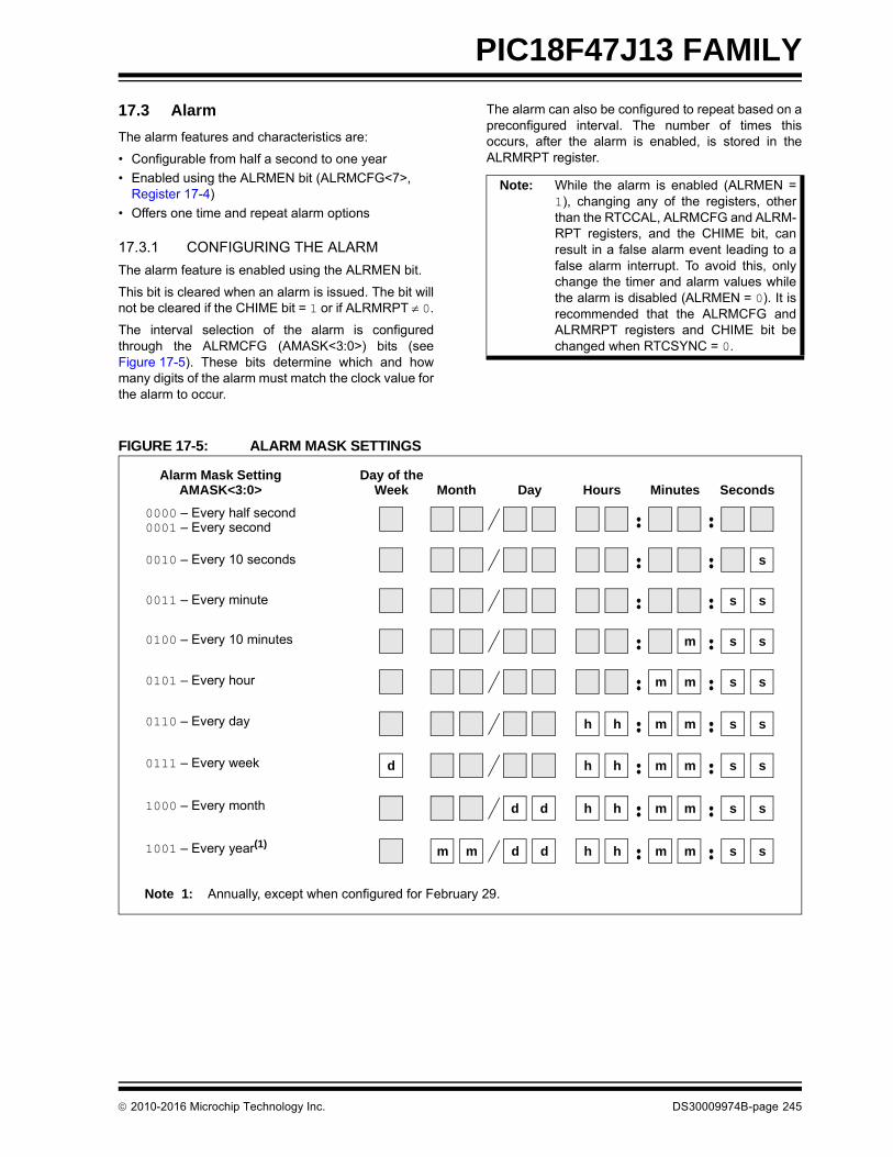
2010-2016 Microchip Technology Inc. DS30009974B-page 245
PIC18F47J13 FAMILY
17.3 Alarm
The alarm features and characteristics are:
• Configurable from half a second to one year
• Enabled using the ALRMEN bit (ALRMCFG<7>, Register 17-4)
• Offers one time and repeat alarm options
17.3.1 CONFIGURING THE ALARM
The alarm feature is enabled using the ALRMEN bit.
This bit is cleared when an alarm is issued. The bit willnot be cleared if the CHIME bit = 1 or if ALRMRPT 0.
The interval selection of the alarm is configuredthrough the ALRMCFG (AMASK<3:0>) bits (seeFigure 17-5). These bits determine which and howmany digits of the alarm must match the clock value forthe alarm to occur.
The alarm can also be configured to repeat based on apreconfigured interval. The number of times thisoccurs, after the alarm is enabled, is stored in theALRMRPT register.
FIGURE 17-5: ALARM MASK SETTINGS
Note: While the alarm is enabled (ALRMEN =1), changing any of the registers, otherthan the RTCCAL, ALRMCFG and ALRM-RPT registers, and the CHIME bit, canresult in a false alarm event leading to afalse alarm interrupt. To avoid this, onlychange the timer and alarm values whilethe alarm is disabled (ALRMEN = 0). It isrecommended that the ALRMCFG andALRMRPT registers and CHIME bit bechanged when RTCSYNC = 0.
Note 1: Annually, except when configured for February 29.
s
s s
m s s
m m s s
h h m m s s
d h h m m s s
d d h h m m s s
m m d d h h m m s s
Day of theWeek Month Day Hours Minutes Seconds
Alarm Mask SettingAMASK<3:0>
0000 – Every half second0001 – Every second
0010 – Every 10 seconds
0011 – Every minute
0100 – Every 10 minutes
0101 – Every hour
0110 – Every day
0111 – Every week
1000 – Every month
1001 – Every year(1)

PIC18F47J13 FAMILY
DS30009974B-page 246 2010-2016 Microchip Technology Inc.
When ALRMCFG = 00 and the CHIME bit = 0(ALRMCFG<6>), the repeat function is disabled andonly a single alarm will occur. The alarm can berepeated up to 255 times by loading the ALRMRPTregister with FFh.
After each alarm is issued, the ALRMRPT register isdecremented by one. Once the register has reached‘00’, the alarm will be issued one last time.
After the alarm is issued a last time, the ALRMEN bit iscleared automatically and the alarm turned off. Indefiniterepetition of the alarm can occur if the CHIME bit = 1.
When CHIME = 1, the alarm is not disabled when theALRMRPT register reaches ‘00’, but it rolls over to FFand continues counting indefinitely.
17.3.2 ALARM INTERRUPT
At every alarm event, an interrupt is generated. Addi-tionally, an alarm pulse output is provided that operatesat half the frequency of the alarm.
The alarm pulse output is completely synchronous withthe RTCC clock and can be used as a trigger clock toother peripherals. This output is available on the RTCCpin. The output pulse is a clock with a 50% duty cycleand a frequency half that of the alarm event (seeFigure 17-6).
The RTCC pin can also output the seconds clock. Theuser can select between the alarm pulse, generated bythe RTCC module, or the seconds clock output.
The RTSECSEL (PADCFG1<2:1>) bits select betweenthese two outputs:
• Alarm pulse – RTSECSEL<2:1> = 00
• Seconds clock – RTSECSEL<2:1> = 01
FIGURE 17-6: TIMER PULSE GENERATION
17.4 Low-Power Modes
The timer and alarm can optionally continue to operatewhile in Sleep, Idle and even Deep Sleep mode. Analarm event can be used to wake-up the microcontrollerfrom any of these Low-Power modes.
17.5 Reset
17.5.1 DEVICE RESET
When a device Reset occurs, the ALCFGRPT registeris forced to its Reset state, causing the alarm to be dis-abled (if enabled prior to the Reset). If the RTCC wasenabled, it will continue to operate when a basic deviceReset occurs.
17.5.2 POWER-ON RESET (POR)
The RTCCFG and ALRMRPT registers are reset onlyon a POR. Once the device exits the POR state, theclock registers should be reloaded with the desiredvalues.
The timer prescaler values can be reset only by writingto the SECONDS register. No device Reset can affectthe prescalers.
RTCEN bit
ALRMEN bit
RTCC Alarm Event
RTCC Pin

2010-2016 Microchip Technology Inc. DS30009974B-page 247
PIC18F47J13 FAMILY
17.6 Register Maps
Table 17-5, Table 17-6 and Table 17-7 summarize theregisters associated with the RTCC module.
TABLE 17-5: RTCC CONTROL REGISTERS
File Name Bit 7 Bit 6 Bit 5 Bit 4 Bit 3 Bit 2 Bit 1 Bit 0All
Resets
RTCCFG RTCEN — RTCWREN RTCSYNC HALFSEC RTCOE RTCPTR1 RTCPTR0 0000
RTCCAL CAL7 CAL6 CAL5 CAL4 CAL3 CAL2 CAL1 CAL0 0000
PADCFG1 — — — — — RTSECSEL1 RTSECSEL0 PMPTTL 0000
ALRMCFG ALRMEN CHIME AMASK3 AMASK2 AMASK1 AMASK0 ALRMPTR1 ALRMPTR0 0000
ALRMRPT ARPT7 ARPT6 ARPT5 ARPT4 ARPT3 ARPT2 ARPT1 ARPT0 0000
PIR3 SSP2IF BCL2IF RC2IF TX2IF TMR4IF CTMUIF TMR3GIF RTCCCIF 0000
PIE3 SSP2IE BCL2IE RC2IE TX2IE TMR4IE CTMUIE TMR3GIE RTCCCIE 0000
IPR3 SSP2IP BCL2IP RC2IP TX2IP TMR4IP CTMUIP TMR3GIP RTCCCIP 0000
Legend: — = unimplemented, read as ‘0’. Reset values are shown in hexadecimal for 44-pin devices.
TABLE 17-6: RTCC VALUE REGISTERS
File Name Bit 7 Bit 6 Bit 5 Bit 4 Bit 3 Bit 2 Bit 1 Bit 0 All Resets
RTCVALH RTCC Value Register Window High Byte, Based on RTCPTR<1:0> xxxx
RTCVALL RTCC Value Register Window Low Byte, Based on RTCPTR<1:0> xxxx
RTCCFG RTCEN — RTCWREN RTCSYNC HALFSEC RTCOE RTCPTR1 RTCPTR0 0000
ALRMCFG ALRMEN CHIME AMASK3 AMASK2 AMASK1 AMASK0 ALRMPTR1 ALRMPTR0 0000
ALRMVALH Alarm Value Register Window High Byte, Based on ALRMPTR<1:0> xxxx
ALRMVALL Alarm Value Register Window Low Byte, Based on ALRMPTR<1:0> xxxx
Legend: — = unimplemented, read as ‘0’. Reset values are shown in hexadecimal for 44-pin devices.
TABLE 17-7: ALARM VALUE REGISTERS
File Name Bit 7 Bit 6 Bit 5 Bit 4 Bit 3 Bit 2 Bit 1 Bit 0All
Resets
ALRMRPT ARPT7 ARPT6 ARPT5 ARPT4 ARPT3 ARPT2 ARPT1 ARPT0 0000
ALRMVALH Alarm Value Register Window High Byte, Based on ALRMPTR<1:0> xxxx
ALRMVALL Alarm Value Register Window Low Byte, Based on ALRMPTR<1:0> xxxx
RTCCAL CAL7 CAL6 CAL5 CAL4 CAL3 CAL2 CAL1 CAL0 0000
RTCVALH RTCC Value Register Window High Byte, Based on RTCPTR<1:0> xxxx
RTCVALL RTCC Value Register Window Low Byte, Based on RTCPTR<1:0> xxxx
Legend: — = unimplemented, read as ‘0’. Reset values are shown in hexadecimal for 44-pin devices.

PIC18F47J13 FAMILY
DS30009974B-page 248 2010-2016 Microchip Technology Inc.
18.0 CAPTURE/COMPARE/PWM (CCP) MODULES
PIC18F47J13 Family devices have seven CCP(Capture/Compare/PWM) modules, designated CCP4through CCP10. All the modules implement standardCapture, Compare and Pulse-Width Modulation (PWM)modes.
Each CCP module contains a 16-bit register that canoperate as a 16-bit Capture register, a 16-bit Compareregister or a PWM Master/Slave Duty Cycle register.For the sake of clarity, all CCP module operation in thefollowing sections is described with respect to CCP4,but is equally applicable to CCP5 through CCP10.
Note: Throughout this section, generic referencesare used for register and bit names that arethe same – except for an ‘x’ variable thatindicates the item’s association with thespecific CCP module. For example, thecontrol register is named CCPxCON andrefers to CCP4CON through CCP10CON.
REGISTER 18-1: CCPxCON: CCP4-10 CONTROL REGISTER (4, BANKED F12h; 5, F0Fh; 6, F0Ch; 7, F09h; 8, F06h; 9, F03h; 10, F00h)
U-0 U-0 R/W-0 R/W-0 R/W-0 R/W-0 R/W-0 R/W-0
— — DCxB1 DCxB0 CCPxM3(1) CCPxM2(1) CCPxM1(1) CCPxM0(1)
bit 7 bit 0
Legend:
R = Readable bit W = Writable bit U = Unimplemented bit, read as ‘0’
-n = Value at POR ‘1’ = Bit is set ‘0’ = Bit is cleared x = Bit is unknown
bit 7-6 Unimplemented: Read as ‘0’
bit 5-4 DCxB<1:0>: PWM Duty Cycle Bit 1 and Bit 0 for CCPx Module
Capture mode:Unused.
Compare mode:Unused.
PWM mode:These bits are the two Least Significant bits (Bit 1 and Bit 0) of the 10-bit PWM duty cycle. The eight Most Significant bits (DCxB<9:2>) of the duty cycle are found in CCPRxL.
bit 3-0 CCPxM<3:0>: CCPx Module Mode Select bits(1)
0000 = Capture/Compare/PWM disabled (resets CCPx module) 0001 = Reserved 0010 = Compare mode, toggle output on match (CCPxIF bit is set) 0011 = Reserved 0100 = Capture mode: every falling edge 0101 = Capture mode: every rising edge0110 = Capture mode: every 4th rising edge 0111 = Capture mode: every 16th rising edge1000 = Compare mode: initialize CCPx pin low; on compare match, force CCPx pin high (CCPxIF bit is set)1001 = Compare mode: initialize CCPx pin high; on compare match, force CCPx pin low (CCPxIF bit is set)1010 = Compare mode: generate software interrupt on compare match (CCPxIF bit is set, CCPx pin
reflects I/O state) 1011 = Compare mode: Special Event Trigger; reset timer on CCPx match (CCPxIF bit is set)11xx = PWM mode
Note 1: CCPxM<3:0> = 1011 will only reset the timer and not start an A/D conversion on CCPx match.

2010-2016 Microchip Technology Inc. DS30009974B-page 249
PIC18F47J13 FAMILY
REGISTER 18-2: CCPTMRS1: CCP4-10 TIMER SELECT 1 REGISTER (BANKED F51h)
R/W-0 R/W-0 U-0 R/W-0 U-0 R/W-0 R/W-0 R/W-0
C7TSEL1 C7TSEL0 — C6TSEL0 — C5TSEL0 C4TSEL1 C4TSEL0
bit 7 bit 0
Legend:
R = Readable bit W = Writable bit U = Unimplemented bit, read as ‘0’
-n = Value at POR ‘1’ = Bit is set ‘0’ = Bit is cleared x = Bit is unknown
bit 7-6 C7TSEL<1:0>: CCP7 Timer Selection bit
00 = CCP7 is based off of TMR1/TMR201 = CCP7 is based off of TMR5/TMR410 = CCP7 is based off of TMR5/TMR611 = CCP7 is based off of TMR5/TMR8
bit 5 Unimplemented: Read as ‘0’
bit 4 C6TSEL0: CCP6 Timer Selection bit
0 = CCP6 is based off of TMR1/TMR21 = CCP6 is based off of TMR5/TMR2
bit 3 Unimplemented: Read as ‘0’
bit 2 C5TSEL0: CCP5 Timer Selection bit
0 = CCP5 is based off of TMR1/TMR21 = CCP5 is based off of TMR5/TMR4
bit 1-0 C4TSEL<1:0>: CCP4 Timer Selection bits
00 = CCP4 is based off of TMR1/TMR201 = CCP4 is based off of TMR3/TMR410 = CCP4 is based off of TMR3/TMR611 = Reserved; do not use

PIC18F47J13 FAMILY
DS30009974B-page 250 2010-2016 Microchip Technology Inc.
REGISTER 18-3: CCPTMRS2: CCP4-10 TIMER SELECT 2 REGISTER (BANKED F50h)
U-0 U-0 U-0 R/W-0 U-0 R/W-0 R/W-0 R/W-0
— — — C10TSEL0 — C9TSEL0 C8TSEL1 C8TSEL0
bit 7 bit 0
Legend:
R = Readable bit W = Writable bit U = Unimplemented bit, read as ‘0’
-n = Value at POR ‘1’ = Bit is set ‘0’ = Bit is cleared x = Bit is unknown
bit 7-5 Unimplemented: Read as ‘0’
bit 4 C10TSEL0: CCP10 Timer Selection bit
0 = CCP10 is based off of TMR1/TMR21 = Reserved; do not use
bit 3 Unimplemented: Read as ‘0’
bit 2 C9TSEL0: CCP9 Timer Selection bit
0 = CCP9 is based off of TMR1/TMR21 = CCP9 is based off of TMR1/TMR4
bit 1-0 C8TSEL<1:0>: CCP8 Timer Selection bits
00 = CCP8 is based off of TMR1/TMR201 = CCP8 is based off of TMR1/TMR410 = CCP8 is based off of TMR1/TMR611 = Reserved; do not use

2010-2016 Microchip Technology Inc. DS30009974B-page 251
PIC18F47J13 FAMILY
REGISTER 18-4: CCPRxL: CCP4-10 PERIOD LOW BYTE REGISTER (4, BANKED F13h; 5, F10h; 6, F0Dh; 7, F0Ah; 8, F07h; 9, F04h; 10, F01h)
R/W-x R/W-x R/W-x R/W-x R/W-x R/W-x R/W-x R/W-x
CCPRxL7 CCPRxL6 CCPRxL5 CCPRxL4 CCPRxL3 CCPRxL2 CCPRxL1 CCPRxL0
bit 7 bit 0
Legend:
R = Readable bit W = Writable bit U = Unimplemented bit, read as ‘0’
-n = Value at POR ‘1’ = Bit is set ‘0’ = Bit is cleared x = Bit is unknown
bit 7-0 CCPRxL<7:0>: CCPx Period Register Low Byte bits
Capture Mode: Capture register low byteCompare Mode: Compare register low bytePWM Mode: PWM Period register low byte
REGISTER 18-5: CCPRxH: CCP4-10 PERIOD HIGH BYTE REGISTER (4, BANKED F14h; 5, F11h; 6, F0Eh; 7, F0Bh; 8, F08h; 9, F05h; 10, F02h)
R/W-x R/W-x R/W-x R/W-x R/W-x R/W-x R/W-x R/W-x
CCPRxH7 CCPRxH6 CCPRxH5 CCPRxH4 CCPRxH3 CCPRxH2 CCPRxH1 CCPRxH0
bit 7 bit 0
Legend:
R = Readable bit W = Writable bit U = Unimplemented bit, read as ‘0’
-n = Value at POR ‘1’ = Bit is set ‘0’ = Bit is cleared x = Bit is unknown
bit 7-0 CCPRxH<7:0>: CCPx Period Register High Byte bits
Capture Mode: Capture register high byteCompare Mode: Compare register high bytePWM Mode: PWM Period register high byte

PIC18F47J13 FAMILY
DS30009974B-page 252 2010-2016 Microchip Technology Inc.
18.1 CCP Module Configuration
Each Capture/Compare/PWM module is associatedwith a control register (generically, CCPxCON) and adata register (CCPRx). The data register, in turn, iscomprised of two 8-bit registers: CCPRxL (low byte)and CCPRxH (high byte). All registers are bothreadable and writable.
18.1.1 CCP MODULES AND TIMER RESOURCES
The CCP modules utilize Timers, 1 through 8, varyingwith the selected mode. Various timers are available tothe CCP modules in Capture, Compare or PWMmodes, as shown in Table 18-1.
TABLE 18-1: CCP MODE – TIMER RESOURCE
The assignment of a particular timer to a module isdetermined by the Timer to CCP enable bits in theCCPTMRSx registers. (See Register 18-2 andRegister 18-3.) All of the modules may be active atonce and may share the same timer resource if theyare configured to operate in the same mode(Capture/Compare or PWM), at the same time.
The CCPTMRS1 register selects the timers for CCPmodules, 7, 6, 5 and 4, and the CCPTMRS2 registerselects the timers for CCP modules, 10, 9 and 8. Thepossible configurations are shown in Table 18-2 andTable 18-3.
TABLE 18-2: TIMER ASSIGNMENTS FOR CCP MODULES 4, 5, 6 AND 7
TABLE 18-3: TIMER ASSIGNMENTS FOR CCP MODULES 8, 9 AND 10
CCP Mode Timer Resource
CaptureTimer1, Timer3 or Timer5
Compare
PWM Timer2, Timer4, Timer6 or Timer8
CCPTMRS1 Register
CCP4 CCP5 CCP6 CCP7
C4TSEL<1:0>
Capture/Compare
Mode
PWMMode
C5TSEL0Capture/Compare
Mode
PWMMode
C6TSEL0Capture/Compare
Mode
PWMMode
C7TSEL<1:0>
Capture/Compare
Mode
PWMMode
0 0 TMR1 TMR2 0 TMR1 TMR2 0 TMR1 TMR2 0 0 TMR1 TMR2
0 1 TMR3 TMR4 1 TMR5 TMR4 1 TMR5 TMR2 0 1 TMR5 TMR4
1 0 TMR3 TMR6 1 0 TMR5 TMR6
1 1 Reserved(1) 1 1 TMR5 TMR8
Note 1: Do not use the reserved bit configuration.
CCPTMRS2 Register
CCP8CCP8
Devices with 64 KbyteCCP9 CCP10
C8TSEL<1:0>
Capture/Compare
Mode
PWMMode
C8TSEL<1:0>
Capture/Compare
Mode
PWMMode
C9TSEL0Capture/Compare
Mode
PWMMode
C10TSEL0Capture/Compare
Mode
PWMMode
0 0 TMR1 TMR2 0 0 TMR1 TMR2 0 TMR1 TMR2 0 TMR1 TMR2
0 1 TMR1 TMR4 0 1 TMR1 TMR4 1 TMR1 TMR4 1 Reserved(1)
1 0 TMR1 TMR6 1 0 TMR1 TMR6
1 1 Reserved(1) 1 1 Reserved(1)
Note 1: Do not use the reserved bit configuration.

2010-2016 Microchip Technology Inc. DS30009974B-page 253
PIC18F47J13 FAMILY
18.1.2 OPEN-DRAIN OUTPUT OPTION
When operating in Output mode (the Compare or PWMmodes), the drivers for the CCPx pins can be optionallyconfigured as open-drain outputs. This feature allowsthe voltage level on the pin to be pulled to a higher levelthrough an external pull-up resistor and allows theoutput to communicate with external circuits without theneed for additional level shifters.
The open-drain output option is controlled by theCCPxOD bits (ODCON1<7:0> and ODCON2<3:2>).Setting the appropriate bit configures the pin for thecorresponding module for open-drain operation.
18.2 Capture Mode
In Capture mode, the CCPR4H:CCPR4L register paircaptures the 16-bit value of the TMR1 or TMR3 registerwhen an event occurs on the CCP4 pin, RB4. An eventis defined as one of the following:
• Every falling edge
• Every rising edge
• Every 4th rising edge
• Every 16th rising edge
The event is selected by the mode select bits,CCP4M<3:0> (CCP4CON<3:0>). When a capture ismade, the interrupt request flag bit, CCP4IF (PIR4<1>),is set. (It must be cleared in software.) If anothercapture occurs before the value in register, CCPR4, isread, the old captured value is overwritten by the newcaptured value.
Figure 18-1 shows the Capture mode block diagram.
18.2.1 CCP PIN CONFIGURATION
In Capture mode, the appropriate CCPx pin should beconfigured as an input by setting the correspondingTRISx direction bit.
18.2.2 TIMER1/3/5 MODE SELECTION
For the available timers (1/3/5) to be used for the capturefeature, the used timers must be running in Timer modeor Synchronized Counter mode. In AsynchronousCounter mode, the capture operation may not work.
The timer to be used with each CCP module is selectedin the CCPTMRSx registers. (See Section 18.1.1 “CCPModules and Timer Resources”.)
Details of the timer assignments for the CCP modulesare given in Table 18-2 and Table 18-3.
FIGURE 18-1: CAPTURE MODE OPERATION BLOCK DIAGRAM
Note: If RB4 is configured as a CCP4 output, awrite to the port causes a capture condi-tion.
CCPR5H CCPR5L
TMR1H TMR1L
Set CCP5IF
TMR5Enable
Q1:Q4
CCP5CON<3:0>
CCP5 Pin
Prescaler 1, 4, 16
andEdge Detect
TMR1Enable
C5TSEL0
C5TSEL0
CCPR4H CCPR4L
TMR1H TMR1L
Set CCP4IF
TMR3Enable
CCP4CON<3:0>
CCP4 Pin
Prescaler 1, 4, 16
TMR3H TMR3L
TMR1Enable
C4TSEL0C4TSEL1
C4TSEL0C4TSEL1
TMR5H TMR5L
andEdge Detect
4
4
4
Note: This block diagram uses CCP4 and CCP5, and their appropriate timers as an example. For details on all ofthe CCP modules and their timer assignments, see Table 18-2 and Table 18-3.

PIC18F47J13 FAMILY
DS30009974B-page 254 2010-2016 Microchip Technology Inc.
18.2.3 SOFTWARE INTERRUPT
When the Capture mode is changed, a false captureinterrupt may be generated. The user should keep theCCP4IE bit (PIE4<1>) clear to avoid false interruptsand should clear the flag bit, CCP4IF, following anysuch change in operating mode.
18.2.4 CCP PRESCALER
There are four prescaler settings in Capture mode.They are specified as part of the operating modeselected by the mode select bits (CCP4M<3:0>).Whenever the CCP module is turned off, or the CCPmodule is not in Capture mode, the prescaler counteris cleared. This means that any Reset will clear theprescaler counter.
Switching from one capture prescaler to another maygenerate an interrupt. Doing that also will not clear theprescaler counter – meaning the first capture may befrom a non-zero prescaler.
Example 18-1 shows the recommended method forswitching between capture prescalers. This examplealso clears the prescaler counter and will not generatethe “false” interrupt.
EXAMPLE 18-1: CHANGING BETWEEN CAPTURE PRESCALERS
18.3 Compare Mode
In Compare mode, the 16-bit CCPR4 register value isconstantly compared against either the TMR1 or TMR3register pair value. When a match occurs, the CCP4pin can be:
• Driven high
• Driven low
• Toggled (high-to-low or low-to-high)
• Unchanged (that is, reflecting the state of the I/O latch)
The action on the pin is based on the value of the modeselect bits (CCP4M<3:0>). At the same time, theinterrupt flag bit, CCP4IF, is set.
Figure 18-2 gives the Compare mode block diagram
18.3.1 CCP PIN CONFIGURATION
The user must configure the CCPx pin as an output byclearing the appropriate TRISx bit.
18.3.2 TIMER1/3/5 MODE SELECTION
If the CCP module is using the compare feature inconjunction with any of the Timer1/3/5 timers, the tim-ers must be running in Timer mode or SynchronizedCounter mode. In Asynchronous Counter mode, thecompare operation may not work.
18.3.3 SOFTWARE INTERRUPT MODE
When the Generate Software Interrupt mode is chosen(CCP4M<3:0> = 1010), the CCP4 pin is not affected.Only a CCP interrupt is generated, if enabled, and theCCP4IE bit is set.
18.3.4 SPECIAL EVENT TRIGGER
Both CCP modules are equipped with a Special EventTrigger. This is an internal hardware signal generatedin Compare mode to trigger actions by other modules.The Special Event Trigger is enabled by selectingthe Compare Special Event Trigger mode(CCP4M<3:0> = 1011).
For either CCP module, the Special Event Trigger resetsthe Timer register pair for whichever timer resource iscurrently assigned as the module’s time base. Thisallows the CCPRx registers to serve as a programmableperiod register for either timer.
The Special Event Trigger for CCP4 cannot start anA/D conversion.
CLRF CCP4CON ; Turn CCP module offMOVLW NEW_CAPT_PS ; Load WREG with the
; new prescaler mode; value and CCP ON
MOVWF CCP4CON ; Load CCP4CON with; this value
Note: Clearing the CCP4CON register will forcethe RB4 compare output latch (dependingon device configuration) to the default lowlevel. This is not the PORTB I/O datalatch.
Note: Details of the timer assignments for theCCP modules are given in Table 18-2 andTable 18-3.
Note: The Special Event Trigger of ECCP1 canstart an A/D conversion, but the A/DConverter must be enabled. For moreinformation, see Section 19.0 “EnhancedCapture/Compare/PWM (ECCP) Module”.

2010-2016 Microchip Technology Inc. DS30009974B-page 255
PIC18F47J13 FAMILY
FIGURE 18-2: COMPARE MODE OPERATION BLOCK DIAGRAM
CCPR5H CCPR5L
TMR1H TMR1L
ComparatorQS
R
OutputLogic
Special Event Trigger
Set CCP5IF
CCP5 Pin
TRIS
CCP5CON<3:0>
Output Enable
TMR5H TMR5L 1
0
Compare
4
(Timer1/5 Reset)
Match
Note: This block diagram uses CCP4 and CCP5 and their appropriate timers as an example. For details on all ofthe CCP modules and their timer assignments, see Table 18-2 and Table 18-3.
TMR1H TMR1L
TMR5H TMR5L
CCPR4H CCPR4L
Comparator
C4TSEL1
Set CCP4IF
1
0
QS
R
OutputLogic
Special Event Trigger
CCP4 Pin
TRIS
CCP4CON<3:0>
Output Enable4
(Timer1/Timer3 Reset, A/D Trigger)
CompareMatch
C5TSEL0
C4TSEL0

PIC18F47J13 FAMILY
DS30009974B-page 256 2010-2016 Microchip Technology Inc.
TABLE 18-4: REGISTERS ASSOCIATED WITH CAPTURE, COMPARE, TIMER1/3/5/7
Name Bit 7 Bit 6 Bit 5 Bit 4 Bit 3 Bit 2 Bit 1 Bit 0
INTCON GIE/GIEH PEIE/GIEL TMR0IE INT0IE RBIE TMR0IF INT0IF RBIF
RCON IPEN — CM RI TO PD POR BOR
PIR4 CCP10IF CCP9IF CCP8IF CCP7IF CCP6IF CCP5IF CCP4IF CCP3IF
PIE4 CCP10IE CCP9IE CCP8IE CCP7IE CCP6IE CCP5IE CCP4IE CCP3IE
IPR4 CCP10IP CCP9IP CCP8IP CCP7IP CCP6IP CCP5IP CCP4IP CCP3IP
TRISB TRISB7 TRISB6 TRISB5 TRISB4 TRISB3 TRISB2 TRISB1 TRISB0
TRISC TRISC7 TRISC6 TRISC5 TRISC4 TRISC3 TRISC2 TRISC1 TRISC0
TRISE RDPU REPU — — — TRISE2 TRISE1 TRISE0
TMR1L Timer1 Register Low Byte
TMR1H Timer1 Register High Byte
TMR3L Timer3 Register Low Byte
TMR3H Timer3 Register High Byte
TMR5L Timer5 Register Low Byte
TMR5H Timer5 Register High Byte
T1CON TMR1CS1 TMR1CS0 T1CKPS1 T1CKPS0 T1OSCEN T1SYNC RD16 TMR1ON
T3CON TMR3CS1 TMR3CS0 T3CKPS1 T3CKPS0 T3OSCEN T3SYNC RD16 TMR3ON
T5CON TMR5CS1 TMR5CS0 T5CKPS1 T5CKPS0 T5OSCEN T5SYNC RD16 TMR5ON
CCPR4L CCPR4L7 CCPR4L6 CCPR4L5 CCPR4L4 CCPR4L3 CCPR4L2 CCPR4L1 CCPR4L0
CCPR4H CCPR4H7 CCPR4H6 CCPR4H5 CCPR4H4 CCPR4H3 CCPR4H2 CCPR4H1 CCPR4H0
CCPR5L CCPR5L7 CCPR5L6 CCPR5L5 CCPR5L4 CCPR5L3 CCPR5L2 CCPR5L1 CCPR5L0
CCPR5H CCPR5H7 CCPR5H6 CCPR5H5 CCPR5H4 CCPR5H3 CCPR5H2 CCPR5H1 CCPR5H0
CCPR6L CCPR6L7 CCPR6L6 CCPR6L5 CCPR6L4 CCPR6L3 CCPR6L2 CCPR6L1 CCPR6L0
CCPR6H CCPR6H7 CCPR6H6 CCPR6H5 CCPR6H4 CCPR6H3 CCPR6H2 CCPR6H1 CCPR6H0
CCPR7L CCPR7L7 CCPR7L6 CCPR7L5 CCPR7L4 CCPR7L3 CCPR7L2 CCPR7L1 CCPR7L0
CCPR7H CCPR7H7 CCPR7H6 CCPR7H5 CCPR7H4 CCPR7H3 CCPR7H2 CCPR7H1 CCPR7H0
CCPR8L CCPR8L7 CCPR8L6 CCPR8L5 CCPR8L4 CCPR8L3 CCPR8L2 CCPR8L1 CCPR8L0
CCPR8H CCPR8H7 CCPR8H6 CCPR8H5 CCPR8H4 CCPR8H3 CCPR8H2 CCPR8H1 CCPR8H0
CCPR9L CCPR9L7 CCPR9L6 CCPR9L5 CCPR9L4 CCPR9L3 CCPR9L2 CCPR9L1 CCPR9L0
CCPR9H CCPR9H7 CCPR9H6 CCPR9H5 CCPR9H4 CCPR9H3 CCPR9H2 CCPR9H1 CCPR9H0
CCPR10L CCPR10L7 CCPR10L6 CCPR10L5 CCPR10L4 CCPR10L3 CCPR10L2 CCPR10L1 CCPR10L0
CCPR10H CCPR10H7 CCPR10H6 CCPR10H5 CCPR10H4 CCPR10H3 CCPR10H2 CCPR10H1 CCPR10H0
CCP4CON — — DC4B1 DC4B0 CCP4M3 CCP4M2 CCP4M1 CCP4M0
CCP5CON — — DC5B1 DC5B0 CCP5M3 CCP5M2 CCP5M1 CCP5M0
CCP6CON — — DC6B1 DC6B0 CCP6M3 CCP6M2 CCP6M1 CCP6M0
CCP7CON — — DC7B1 DC7B0 CCP7M3 CCP7M2 CCP7M1 CCP7M0
CCP8CON — — DC8B1 DC8B0 CCP8M3 CCP8M2 CCP8M1 CCP8M0
CCP9CON — — DC9B1 DC9B0 CCP9M3 CCP9M2 CCP9M1 CCP9M0
CCP10CON — — DC10B1 DC10B0 CCP10M3 CCP10M2 CCP10M1 CCP10M0
CCPTMRS1 C7TSEL1 C7TSEL0 — C6TSEL0 — C5TSEL0 C4TSEL1 C4TSEL0
CCPTMRS2 — — — C10TSEL0 — C9TSEL0 C8TSEL1 C8TSEL0
Legend: — = unimplemented, read as ‘0’. Shaded cells are not used by capture/compare or Timer1/3/5.

2010-2016 Microchip Technology Inc. DS30009974B-page 257
PIC18F47J13 FAMILY
18.4 PWM Mode
In Pulse-Width Modulation (PWM) mode, the CCP4 pinproduces up to a 10-bit resolution PWM output. Sincethe CCP4 pin is multiplexed with a PORTB data latch,the appropriate TRISx bit must be cleared to make theCCP4 pin an output.
Figure 18-3 shows a simplified block diagram of theCCP1 module in PWM mode.
For a step-by-step procedure on how to set up the CCPmodule for PWM operation, see Section 18.4.3“Setup for PWM Operation”.
FIGURE 18-3: SIMPLIFIED PWM BLOCK DIAGRAM(2)
A PWM output (Figure 18-4) has a time base (period)and a time that the output stays high (duty cycle). Thefrequency of the PWM is the inverse of the period(1/period).
FIGURE 18-4: PWM OUTPUT
18.4.1 PWM PERIOD
The PWM period is specified by writing to the PR2register. The PWM period can be calculated using thefollowing formula:
EQUATION 18-1:
PWM frequency is defined as 1/[PWM period].
When TMR2 is equal to PR2, the following three eventsoccur on the next increment cycle:
• TMR2 is cleared
• The CCP4 pin is set
(An exception: If the PWM duty cycle = 0%, the CCP4 pin will not be set)
• The PWM duty cycle is latched from CCPR4L into CCPR4H
CCPR4L
CCPR4H (Slave)
Comparator
TMR2
Comparator
PR2
(Note 1)
R Q
S
Duty Cycle Registers CCP4CON<5:4>
Clear Timer,CCP1 pin and latch D.C.
TRISC<2>
RC2
Note 1: The 8-bit TMR2 value is concatenated with the 2-bit internal Q clock, or 2 bits of the prescaler, to create the 10-bit time base.
2: CCP4 and its appropriate timers are used as an example. For details on all of the CCP modules and their timer assignments, see Table 18-2 and Table 18-3. Note: The Timer2 postscalers (see
Section 14.0 “Timer2 Module”) are notused in the determination of the PWM fre-quency. The postscaler could be used tohave a servo update rate at a different fre-quency than the PWM output.
Period
Duty Cycle
TMR2 = PR2
TMR2 = Duty Cycle
TMR2 = PR2
PWM Period = [(PR2) + 1] • 4 • TOSC •(TMR2 Prescale Value)

PIC18F47J13 FAMILY
DS30009974B-page 258 2010-2016 Microchip Technology Inc.
18.4.2 PWM DUTY CYCLE
The PWM duty cycle is specified by writing to theCCPR4L register and to the CCP4CON<5:4> bits. Upto 10-bit resolution is available. The CCPR4L containsthe eight MSbs and the CCP4CON<5:4> contains thetwo LSbs. This 10-bit value is represented byCCPR4L:CCP4CON<5:4>. The following equation isused to calculate the PWM duty cycle in time:
EQUATION 18-2:
CCPR4L and CCP4CON<5:4> can be written to at anytime, but the duty cycle value is not latched intoCCPR4H until after a match between PR2 and TMR2occurs (that is, the period is complete). In PWM mode,CCPR4H is a read-only register.
The CCPR4H register and a two-bit internal latch areused to double-buffer the PWM duty cycle. Thisdouble-buffering is essential for glitchless PWMoperation.
When the CCPR4H and two-bit latch match TMR2,concatenated with an internal two-bit Q clock or twobits of the TMR2 prescaler, the CCP4 pin is cleared.
The maximum PWM resolution (bits) for a given PWMfrequency is given by the equation:
EQUATION 18-3:
TABLE 18-5: EXAMPLE PWM FREQUENCIES AND RESOLUTIONS AT 40 MHz
18.4.3 SETUP FOR PWM OPERATION
To configure the CCP module for PWM operation:
1. Set the PWM period by writing to the PR2register.
2. Set the PWM duty cycle by writing to theCCPR4L register and CCP4CON<5:4> bits.
3. Make the CCP4 pin an output by clearing theappropriate TRISx bit.
4. Set the TMR2 prescale value, then enable Tim-er2 by writing to T2CON.
5. Configure the CCP4 module for PWM operation.
PWM Duty Cycle = (CCPR4L:CCP4CON<5:4>) •TOSC • (TMR2 Prescale Value)
Note: If the PWM duty cycle value is longer thanthe PWM period, the CCP4 pin will not becleared.
FOSC
FPWM--------------- log
2 log-----------------------------bits=PWM Resolution (max)
PWM Frequency 2.44 kHz 9.77 kHz 39.06 kHz 156.25 kHz 312.50 kHz 416.67 kHz
Timer Prescaler (1, 4, 16) 16 4 1 1 1 1
PR2 Value FFh FFh FFh 3Fh 1Fh 17h
Maximum Resolution (bits) 10 10 10 8 7 6.58

2010-2016 Microchip Technology Inc. DS30009974B-page 259
PIC18F47J13 FAMILY
TABLE 18-6: REGISTERS ASSOCIATED WITH PWM AND TIMERS
Name Bit 7 Bit 6 Bit 5 Bit 4 Bit 3 Bit 2 Bit 1 Bit 0
INTCON GIE/GIEH PEIE/GIEL TMR0IE INT0IE RBIE TMR0IF INT0IF RBIF
RCON IPEN — CM RI TO PD POR BOR
PIR4 CCP10IF CCP9IF CCP8IF CCP7IF CCP6IF CCP5IF CCP4IF CCP3IF
PIE4 CCP10IE CCP9IE CCP8IE CCP7IE CCP6IE CCP5IE CCP4IE CCP3IE
IPR4 CCP10IP CCP9IP CCP8IP CCP7IP CCP6IP CCP5IP CCP4IP CCP3IP
TRISB TRISB7 TRISB6 TRISB5 TRISB4 TRISB3 TRISB2 TRISB1 TRISB0
TRISC TRISC7 TRISC6 TRISC5 TRISC4 TRISC3 TRISC2 TRISC1 TRISC0
TRISE RDPU REPU — — — TRISE2 TRISE1 TRISE0
TMR2 Timer2 Register
TMR4 Timer4 Register
TMR6 Timer6 Register
TMR8 Timer8 Register
PR2 Timer2 Period Register
PR4 Timer4 Period Register
PR6 Timer6 Period Register
PR8 Timer8 Period Register
T2CON — T2OUTPS3 T2OUTPS2 T2OUTPS1 T2OUTPS0 TMR2ON T2CKPS1 T2CKPS0
T4CON — T4OUTPS3 T4OUTPS2 T4OUTPS1 T4OUTPS0 TMR4ON T4CKPS1 T4CKPS0
T6CON — T6OUTPS3 T6OUTPS2 T6OUTPS1 T6OUTPS0 TMR6ON T6CKPS1 T6CKPS0
T8CON — T8OUTPS3 T8OUTPS2 T8OUTPS1 T8OUTPS0 TMR8ON T8CKPS1 T8CKPS0
CCPR4L CCPR4L7 CCPR4L6 CCPR4L5 CCPR4L4 CCPR4L3 CCPR4L2 CCPR4L1 CCPR4L0
CCPR4H CCPR4H7 CCPR4H6 CCPR4H5 CCPR4H4 CCPR4H3 CCPR4H2 CCPR4H1 CCPR4H0
CCPR5L CCPR5L7 CCPR5L6 CCPR5L5 CCPR5L4 CCPR5L3 CCPR5L2 CCPR5L1 CCPR5L0
CCPR5H CCPR5H7 CCPR5H6 CCPR5H5 CCPR5H4 CCPR5H3 CCPR5H2 CCPR5H1 CCPR5H0
CCPR6L CCPR6L7 CCPR6L6 CCPR6L5 CCPR6L4 CCPR6L3 CCPR6L2 CCPR6L1 CCPR6L0
CCPR6H CCPR6H7 CCPR6H6 CCPR6H5 CCPR6H4 CCPR6H3 CCPR6H2 CCPR6H1 CCPR6H0
CCPR7L CCPR7L7 CCPR7L6 CCPR7L5 CCPR7L4 CCPR7L3 CCPR7L2 CCPR7L1 CCPR7L0
CCPR7H CCPR7H7 CCPR7H6 CCPR7H5 CCPR7H4 CCPR7H3 CCPR7H2 CCPR7H1 CCPR7H0
CCPR8L CCPR8L7 CCPR8L6 CCPR8L5 CCPR8L4 CCPR8L3 CCPR8L2 CCPR8L1 CCPR8L0
CCPR8H CCPR8H7 CCPR8H6 CCPR8H5 CCPR8H4 CCPR8H3 CCPR8H2 CCPR8H1 CCPR8H0
CCPR9L CCPR9L7 CCPR9L6 CCPR9L5 CCPR9L4 CCPR9L3 CCPR9L2 CCPR9L1 CCPR9L0
CCPR9H CCPR9H7 CCPR9H6 CCPR9H5 CCPR9H4 CCPR9H3 CCPR9H2 CCPR9H1 CCPR9H0
CCPR10L CCPR10L7 CCPR10L6 CCPR10L5 CCPR10L4 CCPR10L3 CCPR10L2 CCPR10L1 CCPR10L0
CCPR10H CCPR10H7 CCPR10H6 CCPR10H5 CCPR10H4 CCPR10H3 CCPR10H2 CCPR10H1 CCPR10H0
CCP4CON — — DC4B1 DC4B0 CCP4M3 CCP4M2 CCP4M1 CCP4M0
CCP5CON — — DC5B1 DC5B0 CCP5M3 CCP5M2 CCP5M1 CCP5M0
CCP6CON — — DC6B1 DC6B0 CCP6M3 CCP6M2 CCP6M1 CCP6M0
CCP7CON — — DC7B1 DC7B0 CCP7M3 CCP7M2 CCP7M1 CCP7M0
CCP8CON — — DC8B1 DC8B0 CCP8M3 CCP8M2 CCP8M1 CCP8M0
CCP9CON — — DC9B1 DC9B0 CCP9M3 CCP9M2 CCP9M1 CCP9M0
CCP10CON — — DC10B1 DC10B0 CCP10M3 CCP10M2 CCP10M1 CCP10M0
CCPTMRS1 C7TSEL1 C7TSEL0 — C6TSEL0 — C5TSEL0 C4TSEL1 C4TSEL0
CCPTMRS2 — — — C10TSEL0 — C9TSEL0 C8TSEL1 C8TSEL0
Legend: — = unimplemented, read as ‘0’. Shaded cells are not used by PWM or Timer2/4/6/8.

PIC18F47J13 FAMILY
DS30009974B-page 260 2010-2016 Microchip Technology Inc.
19.0 ENHANCED CAPTURE/COMPARE/PWM (ECCP) MODULE
PIC18F47J13 Family devices have three EnhancedCapture/Compare/PWM (ECCP) modules: ECCP1,ECCP2 and ECCP3. These modules contain a 16-bitregister, which can operate as a 16-bit Capture register,a 16-bit Compare register or a PWM Master/Slave DutyCycle register. These ECCP modules are upwardlycompatible with CCP.
The ECCP modules are implemented as standard CCPmodules with enhanced PWM capabilities. Theseinclude:
• Provision for two or four output channels
• Output Steering modes
• Programmable polarity
• Programmable dead-band control
• Automatic shutdown and restart
The enhanced features are discussed in detail inSection 19.4 “PWM (Enhanced Mode)”.
Note: Throughout this section, generic referencesare used for register and bit names that arethe same – except for an ‘x’ variable thatindicates the item’s association with theECCP1, ECCP2 or ECCP3 module. Forexample, the control register is namedCCPxCON and refers to CCP1CON,CCP2CON and CCP3CON.

2010-2016 Microchip Technology Inc. DS30009974B-page 261
PIC18F47J13 FAMILY
REGISTER 19-1: CCPxCON: ECCP1/2/3 CONTROL (1, ACCESS FBAh; 2, FB4h; 3, BANKED F15h)
R/W-0 R/W-0 R/W-0 R/W-0 R/W-0 R/W-0 R/W-0 R/W-0
PxM1 PxM0 DCxB1 DCxB0 CCPxM3 CCPxM2 CCPxM1 CCPxM0
bit 7 bit 0
Legend:
R = Readable bit W = Writable bit U = Unimplemented bit, read as ‘0’
-n = Value at POR ‘1’ = Bit is set ‘0’ = Bit is cleared x = Bit is unknown
bit 7-6 PxM<1:0>: Enhanced PWM Output Configuration bits
If CCPxM<3:2> = 00, 01, 10:xx = PxA assigned as capture/compare input/output; PxB, PxC and PxD assigned as port pins
If CCPxM<3:2> = 11:00 = Single output: PxA, PxB, PxC and PxD are controlled by steering (see Section 19.4.7 “Pulse
Steering Mode”)01 = Full-bridge output forward: PxD modulated; PxA active; PxB, PxC inactive10 = Half-bridge output: PxA, PxB modulated with dead-band control; PxC and PxD assigned as
port pins11 = Full-bridge output reverse: PxB modulated; PxC active; PxA and PxD inactive
bit 5-4 DCxB<1:0>: PWM Duty Cycle Bit 1 and Bit 0
Capture mode:Unused.
Compare mode:Unused.
PWM mode:These bits are the two LSbs of the 10-bit PWM duty cycle. The eight MSbs of the duty cycle are found in ECCPRxL.
bit 3-0 CCPxM<3:0>: ECCPx Mode Select bits
0000 = Capture/Compare/PWM off (resets ECCPx module)0001 = Reserved0010 = Compare mode; toggle output on match0011 = Capture mode0100 = Capture mode; every falling edge0101 = Capture mode; every rising edge0110 = Capture mode; every fourth rising edge 0111 = Capture mode; every 16th rising edge1000 = Compare mode; initialize ECCPx pin low, set output on compare match (set CCPxIF)1001 = Compare mode; initialize ECCPx pin high, clear output on compare match (set CCPxIF)1010 = Compare mode; generate software interrupt only, ECCPx pin reverts to I/O state1011 = Compare mode; trigger special event (ECCPx resets TMR1 or TMR3, starts A/D conversion,
sets CCPxIF bit)1100 = PWM mode; PxA and PxC active-high; PxB and PxD active-high1101 = PWM mode; PxA and PxC active-high; PxB and PxD active-low1110 = PWM mode; PxA and PxC active-low; PxB and PxD active-high1111 = PWM mode; PxA and PxC active-low; PxB and PxD active-low

PIC18F47J13 FAMILY
DS30009974B-page 262 2010-2016 Microchip Technology Inc.
In addition to the expanded range of modes availablethrough the CCPxCON and ECCPxAS registers, theECCP modules have two additional registers associatedwith Enhanced PWM operation and auto-shutdownfeatures. They are:
• ECCPxDEL – Enhanced PWM Control
• PSTRxCON – Pulse Steering Control
REGISTER 19-2: CCPTMRS0: ECCP1/2/3 TIMER SELECT 0 REGISTER (BANKED F52h)
R/W-0 R/W-0 R/W-0 R/W-0 R/W-0 R/W-0 R/W-0 R/W-0
C3TSEL1 C3TSEL0 C2TSEL2 C2TSEL1 C2TSEL0 C1TSEL2 C1TSEL1 C1TSEL0
bit 7 bit 0
Legend:
R = Readable bit W = Writable bit U = Unimplemented bit, read as ‘0’
-n = Value at POR ‘1’ = Bit is set ‘0’ = Bit is cleared x = Bit is unknown
bit 7-6 C3TSEL<1:0>: ECCP3 Timer Selection bits
00 = ECCP3 is based off of TMR1/TMR201 = ECCP3 is based off of TMR3/TMR410 = ECCP3 is based off of TMR3/TMR611 = ECCP3 is based off of TMR3/TMR8
bit 5-3 C2TSEL<2:0>: ECCP2 Timer Selection bits
000 = ECCP2 is based off of TMR1/TMR2001 = ECCP2 is based off of TMR3/TMR4010 = ECCP2 is based off of TMR3/TMR6011 = ECCP2 is based off of TMR3/TMR81xx = Reserved; do not use
bit 2-0 C1TSEL<2:0>: ECCP1 Timer Selection bits
000 = ECCP1 is based off of TMR1/TMR2001 = ECCP1 is based off of TMR3/TMR4010 = ECCP1 is based off of TMR3/TMR6011 = ECCP1 is based off of TMR3/TMR81xx = Reserved; do not use

2010-2016 Microchip Technology Inc. DS30009974B-page 263
PIC18F47J13 FAMILY
19.1 ECCP Outputs and Configuration
The Enhanced CCP module may have up to four PWMoutputs, depending on the selected operating mode.These outputs, designated PxA through PxD, arerouted through the Peripheral Pin Select (PPS)module. Therefore, individual functions can be mappedto any of the remappable I/O pins (RPn).
The outputs that are active depend on the ECCPoperating mode selected. The pin assignments aresummarized in Table 19-3.
To configure the I/O pins as PWM outputs, the properPWM mode must be selected by setting the PxM<1:0>and CCPxM<3:0> bits. The appropriate TRIS directionbits for the port pins must also be set as outputs.
19.1.1 ECCP MODULE AND TIMER RESOURCES
The ECCP modules use Timer1, 2, 3, 4, 6 or 8, depend-ing on the mode selected. These timers are available toCCP modules in Capture, Compare or PWM modes, asshown in Table 19-1.
TABLE 19-1: ECCP MODE – TIMER RESOURCE
The assignment of a particular timer to a module isdetermined by the Timer to ECCP enable bits in theCCPTMRS0 register (Register 19-2). The interactionsbetween the two modules are depicted in Figure 19-1.Capture operations are designed to be used when thetimer is configured for Synchronous Counter mode.Capture operations may not work as expected if theassociated timer is configured for Asynchronous Countermode.
19.2 Capture Mode
In Capture mode, the CCPRxH:CCPRxL register paircaptures the 16-bit value of the TMR1 or TMR3registers when an event occurs on the correspondingECCPx pin. An event is defined as one of the following:
• Every falling edge
• Every rising edge
• Every fourth rising edge
• Every 16th rising edge
The event is selected by the mode select bits,CCPxM<3:0> (CCPxCON register<3:0>). When acapture is made, the interrupt request flag bit, CCPxIF,is set (see Table 19-2). The flag must be cleared bysoftware. If another capture occurs before the value inthe CCPRxH/L register pair is read, the old capturedvalue is overwritten by the new captured value.
19.2.1 ECCP PIN CONFIGURATION
In Capture mode, the appropriate ECCPx pin should beconfigured as an input by setting the correspondingTRISx direction bit.
Additionally, the ECCPx input function needs to beassigned to an I/O pin through the Peripheral PinSelect module. For details on setting up theremappable pins, see Section 10.7 “Peripheral PinSelect (PPS)”.
ECCP Mode Timer Resource
Capture Timer1 or Timer3
Compare Timer1 or Timer3
PWM Timer2, Timer4, Timer6 or Timer8
TABLE 19-2: ECCP1/2/3 INTERRUPT FLAG BITS
ECCP Module Flag-Bit
1 PIR1<2>
2 PIR2<0>
3 PIR4<0>
Note: If the ECCPx pin is configured as an out-put, a write to the port can cause a capturecondition.

PIC18F47J13 FAMILY
DS30009974B-page 264 2010-2016 Microchip Technology Inc.
19.2.2 TIMER1/TIMER3 MODE SELECTION
The timers that are to be used with the capture feature(Timer1 and/or Timer3) must be running in Timer modeor Synchronized Counter mode. In AsynchronousCounter mode, the capture operation may not work.The timer to be used with each ECCP module isselected in the CCPTMRS0 register (Register 19-2).
19.2.3 SOFTWARE INTERRUPT
When the Capture mode is changed, a false captureinterrupt may be generated. The user should keep theCCPxIE interrupt enable bit clear to avoid false interrupts.The interrupt flag bit, CCPxIF, should also be clearedfollowing any such change in operating mode.
19.2.4 ECCP PRESCALER
There are four prescaler settings in Capture mode; theyare specified as part of the operating mode selected bythe mode select bits (CCPxM<3:0>). Whenever the
ECCP module is turned off, or Capture mode isdisabled, the prescaler counter is cleared. This meansthat any Reset will clear the prescaler counter.
Switching from one capture prescaler to another maygenerate an interrupt. Also, the prescaler counter willnot be cleared; therefore, the first capture may be froma non-zero prescaler. Example 19-1 provides therecommended method for switching between captureprescalers. This example also clears the prescalercounter and will not generate the “false” interrupt.
EXAMPLE 19-1: CHANGING BETWEEN CAPTURE PRESCALERS
FIGURE 19-1: CAPTURE MODE OPERATION BLOCK DIAGRAM
CLRF ECCP1CON ; Turn ECCP module offMOVLW NEW_CAPT_PS ; Load WREG with the
; new prescaler mode; value and ECCP ON
MOVWF CCP1CON ; Load ECCP1CON with; this value
CCPR1H CCPR1L
TMR1H TMR1L
Set CCP1IF
TMR3Enable
Q1:Q4
CCP1CON<3:0>
ECCP1 PinPrescaler 1, 4, 16
andEdge Detect
TMR1Enable
C1TSEL0
TMR3H TMR3L
4
4
C1TSEL1C1TSEL2
C1TSEL0C1TSEL1C1TSEL2

2010-2016 Microchip Technology Inc. DS30009974B-page 265
PIC18F47J13 FAMILY
19.3 Compare Mode
In Compare mode, the 16-bit CCPRx register pair valueis constantly compared against either the TMR1 orTMR3 register pair value. When a match occurs, theECCPx pin can be:
• Driven high
• Driven low
• Toggled (high-to-low or low-to-high)
• Unchanged (that is, reflecting the state of the I/O latch)
The action on the pin is based on the value of the modeselect bits (CCPxM<3:0>). At the same time, theinterrupt flag bit, CCPxIF, is set.
19.3.1 ECCP PIN CONFIGURATION
Users must configure the ECCPx pin as an output byclearing the appropriate TRISx bit.
19.3.2 TIMER1/TIMER3 MODE SELECTION
Timer1 and/or Timer3 must be running in Timer modeor Synchronized Counter mode if the ECCP module isusing the compare feature. In Asynchronous Countermode, the compare operation will not work reliably.
19.3.3 SOFTWARE INTERRUPT MODE
When the Generate Software Interrupt mode is chosen(CCPxM<3:0> = 1010), the ECCPx pin is not affected;only the CCPxIF interrupt flag is affected.
19.3.4 SPECIAL EVENT TRIGGER
The ECCP module is equipped with a Special EventTrigger. This is an internal hardware signal generatedin Compare mode to trigger actions by other modules.The Special Event Trigger is enabled by selectingthe Compare Special Event Trigger mode(CCPxM<3:0> = 1011).
The Special Event Trigger resets the Timer register pairfor whichever timer resource is currently assigned as themodule’s time base. This allows the CCPRx registers toserve as a Programmable Period register for eithertimer.
The Special Event Trigger can also start an A/D conver-sion. In order to do this, the A/D Converter mustalready be enabled.
FIGURE 19-2: COMPARE MODE OPERATION BLOCK DIAGRAM
Note: Clearing the CCPxCON register will forcethe ECCPx compare output latch(depending on device configuration) to thedefault low level. This is not the PORTxI/O data latch.
TMR1H TMR1L
TMR3H TMR3L
CCPR1H CCPR1L
Comparator
Set CCP1IF
1
0
QS
R
OutputLogic
ECCP1 Pin
TRIS
CCP1CON<3:0>
Output Enable4
(Timer1/Timer3 Reset, A/D Trigger)
CompareMatch
C1TSEL0C1TSEL1C1TSEL2
Special Event Trigger

PIC18F47J13 FAMILY
DS30009974B-page 266 2010-2016 Microchip Technology Inc.
19.4 PWM (Enhanced Mode)
The Enhanced PWM mode can generate a PWM signalon up to four different output pins with up to 10 bits ofresolution. It can do this through four different PWMOutput modes:
• Single PWM mode
• Half-Bridge PWM mode
• Full-Bridge PWM, Forward mode
• Full-Bridge PWM, Reverse mode
To select an Enhanced PWM mode, the PxM bits of theCCPxCON register must be set appropriately.
The PWM outputs are multiplexed with I/O pins and aredesignated: PxA, PxB, PxC and PxD. The polarity of thePWM pins is configurable and is selected by setting theCCPxM bits in the CCPxCON register appropriately.
Table 19-1 provides the pin assignments for eachEnhanced PWM mode.
Figure 19-3 provides an example of a simplified blockdiagram of the Enhanced PWM module.
FIGURE 19-3: SIMPLIFIED BLOCK DIAGRAM OF THE ENHANCED PWM MODE EXAMPLE
Note: To prevent the generation of anincomplete waveform when the PWM isfirst enabled, the ECCP module waits untilthe start of a new PWM period beforegenerating a PWM signal.
Note 1: The TRIS register value for each PWM output must be configured appropriately.
2: Any pin not used by an Enhanced PWM mode is available for alternate pin functions.
CCPR1L
CCPR1H (Slave)
Comparator
TMR2
Comparator
PR2
(1)
R Q
S
Duty Cycle RegistersDC1B<1:0>
Clear Timer2,Toggle PWM Pin and Latch Duty Cycle
Note 1: The 8-bit timer, TMR2 register, is concatenated with the 2-bit internal Q clock, or 2 bits of the prescaler, tocreate the 10-bit time base.
TRIS
ECCPx/Output Pin
TRIS
Output Pin
TRIS
Output Pin
TRIS
Output Pin
OutputController
PxM<1:0>2
CCPxM<3:0>4
ECCP1DEL
ECCPx/PxA
PxB
PxC
PxD

2010-2016 Microchip Technology Inc. DS30009974B-page 267
PIC18F47J13 FAMILY
TABLE 19-3: EXAMPLE PIN ASSIGNMENTS FOR VARIOUS PWM ENHANCED MODES
FIGURE 19-4: PWM (ENHANCED MODE) OUTPUT RELATIONSHIPS (ACTIVE-HIGH STATE) EXAMPLE
TABLE 19-3:
ECCP Mode PxM<1:0> PxA PxB PxC PxD
Single 00 Yes(1) Yes(1) Yes(1) Yes(1)
Half-Bridge 10 Yes Yes No No
Full-Bridge, Forward 01 Yes Yes Yes Yes
Full-Bridge, Reverse 11 Yes Yes Yes Yes
Note 1: Outputs are enabled by pulse steering in Single mode (see Register 19-6).
0
Period
00
10
01
11
SignalPR2 + 1
PxM<1:0>
PxA Modulated
PxA Modulated
PxB Modulated
PxA Active
PxB Inactive
PxC Inactive
PxD Modulated
PxA Inactive
PxB Modulated
PxC Active
PxD Inactive
Pulse Width
(Single Output)
(Half-Bridge)
(Full-Bridge,Forward)
(Full-Bridge,Reverse)
Delay(1) Delay(1)
Relationships:• Period = 4 * TOSC * (PR2 + 1) * (TMR2 Prescale Value)• Pulse Width = TOSC * (CCPRxL<7:0>:CCPxCON<5:4>) * (TMR2 Prescale Value)• Delay = 4 * TOSC * (ECCPxDEL<6:0>)
Note 1: Dead-band delay is programmed using the ECCPxDEL register (see Section 19.4.6 “ProgrammableDead-Band Delay Mode”).

PIC18F47J13 FAMILY
DS30009974B-page 268 2010-2016 Microchip Technology Inc.
FIGURE 19-5: ENHANCED PWM OUTPUT RELATIONSHIPS (ACTIVE-LOW STATE) EXAMPLE
0
Period
00
10
01
11
SignalPR2 + 1
PxM<1:0>
PxA Modulated
PxA Modulated
PxB Modulated
PxA Active
PxB Inactive
PxC Inactive
PxD Modulated
PxA Inactive
PxB Modulated
PxC Active
PxD Inactive
Pulse
Width
(Single Output)
(Half-Bridge)
(Full-Bridge,
Forward)
(Full-Bridge,
Reverse)
Delay(1) Delay(1)
Relationships:• Period = 4 * TOSC * (PR2 + 1) * (TMR2 Prescale Value)• Pulse Width = TOSC * (CCPRxL<7:0>:CCPxCON<5:4>) * (TMR2 Prescale Value)• Delay = 4 * TOSC * (ECCPxDEL<6:0>)
Note 1: Dead-band delay is programmed using the ECCPxDEL register (see Section 19.4.6 “Programmable Dead-BandDelay Mode”).

2010-2016 Microchip Technology Inc. DS30009974B-page 269
PIC18F47J13 FAMILY
19.4.1 HALF-BRIDGE MODE
In Half-Bridge mode, two pins are used as outputs todrive push-pull loads. The PWM output signal is outputon the PxA pin, while the complementary PWM outputsignal is output on the PxB pin (see Figure 19-6). Thismode can be used for half-bridge applications, asshown in Figure 19-7, or for full-bridge applications,where four power switches are being modulated withtwo PWM signals.
In Half-Bridge mode, the programmable dead-band delaycan be used to prevent shoot-through current inhalf-bridge power devices. The value of the PxDC<6:0>bits of the ECCPxDEL register sets the number ofinstruction cycles before the output is driven active. If thevalue is greater than the duty cycle, the correspondingoutput remains inactive during the entire cycle. For moredetails on the dead-band delay operations, seeSection 19.4.6 “Programmable Dead-Band DelayMode”.
Since the PxA and PxB outputs are multiplexed with theport data latches, the associated TRIS bits must becleared to configure PxA and PxB as outputs.
FIGURE 19-6: EXAMPLE OF HALF-BRIDGE PWM OUTPUT
FIGURE 19-7: EXAMPLE OF HALF-BRIDGE APPLICATIONS
Period
Pulse Width
td
td
(1)
PxA(2)
PxB(2)
td = Dead-Band Delay
Period
(1) (1)
Note 1: At this time, the TMR2 register is equal to thePR2 register.
2: Output signals are shown as active-high.
PxA
PxB
FETDriver
FETDriver
Load
+
-
+
-
FETDriver
FETDriver
V+
Load
FETDriver
FETDriver
PxA
PxB
Standard Half-Bridge Circuit (“Push-Pull”)
Half-Bridge Output Driving a Full-Bridge Circuit

PIC18F47J13 FAMILY
DS30009974B-page 270 2010-2016 Microchip Technology Inc.
19.4.2 FULL-BRIDGE MODE
In Full-Bridge mode, all four pins are used as outputs.An example of a full-bridge application is provided inFigure 19-8.
In the Forward mode, the PxA pin is driven to its activestate and the PxD pin is modulated, while the PxB andPxC pins are driven to their inactive state, as shown inFigure 19-9.
In the Reverse mode, the PxC pin is driven to its activestate and the PxB pin is modulated, while the PxA andPxD pins are driven to their inactive state, as shown inFigure 19-9.
The PxA, PxB, PxC and PxD outputs are multiplexedwith the port data latches. The associated TRIS bitsmust be cleared to configure the PxA, PxB, PxC andPxD pins as outputs.
FIGURE 19-8: EXAMPLE OF FULL-BRIDGE APPLICATION
PxA
PxC
FETDriver
FETDriver
V+
V-
Load
FETDriver
FETDriver
PxB
PxD
QA
QB QD
QC

2010-2016 Microchip Technology Inc. DS30009974B-page 271
PIC18F47J13 FAMILY
FIGURE 19-9: EXAMPLE OF FULL-BRIDGE PWM OUTPUT
Period
Pulse Width
PxA(2)
PxB(2)
PxC(2)
PxD(2)
Forward Mode
(1)
Period
Pulse Width
PxA(2)
PxC(2)
PxD(2)
PxB(2)
Reverse Mode
(1)
(1)(1)
Note 1: At this time, the TMR2 register is equal to the PR2 register.
2: The output signal is shown as active-high.

PIC18F47J13 FAMILY
DS30009974B-page 272 2010-2016 Microchip Technology Inc.
19.4.2.1 Direction Change in Full-Bridge Mode
In the Full-Bridge mode, the PxM1 bit in the CCPxCONregister allows users to control the forward/reversedirection. When the application firmware changes thisdirection control bit, the module will change to the newdirection on the next PWM cycle.
A direction change is initiated in software by changingthe PxM1 bit of the CCPxCON register. The followingsequence occurs prior to the end of the current PWMperiod:
• The modulated outputs (PxB and PxD) are placed in their inactive state.
• The associated unmodulated outputs (PxA and PxC) are switched to drive in the opposite direction.
• PWM modulation resumes at the beginning of the next period.
For an illustration of this sequence, see Figure 19-10.
The Full-Bridge mode does not provide a dead-banddelay. As one output is modulated at a time, a dead-banddelay is generally not required. There is a situation wherea dead-band delay is required. This situation occurswhen both of the following conditions are true:
• The direction of the PWM output changes when the duty cycle of the output is at or near 100%.
• The turn-off time of the power switch, including the power device and driver circuit, is greater than the turn-on time.
Figure 19-11 shows an example of the PWM directionchanging from forward to reverse at a near 100% dutycycle. In this example, at time t1, the PxA and PxDoutputs become inactive, while the PxC outputbecomes active. Since the turn-off time of the powerdevices is longer than the turn-on time, a shoot-throughcurrent will flow through power devices, QC and QD(see Figure 19-8), for the duration of ‘t’. The samephenomenon will occur to power devices, QA and QB,for PWM direction change from reverse to forward.
If changing PWM direction at high duty cycle is requiredfor an application, two possible solutions for eliminatingthe shoot-through current are:
• Reduce PWM duty cycle for one PWM period before changing directions.
• Use switch drivers that can drive the switches off faster than they can drive them on.
Other options to prevent shoot-through current mayexist.
FIGURE 19-10: EXAMPLE OF PWM DIRECTION CHANGE
Pulse Width
Period(1)Signal
Note 1: The direction bit, PxM1 of the CCPxCON register, is written any time during the PWM cycle.
2: When changing directions, the PxA and PxC signals switch before the end of the current PWM cycle. Themodulated PxB and PxD signals are inactive at this time. The length of this time is: (1/FOSC) • TMR2 Prescale Value.
Period
(2)
PxA (Active-High)
PxB (Active-High)
PxC (Active-High)
PxD (Active-High)
Pulse Width

2010-2016 Microchip Technology Inc. DS30009974B-page 273
PIC18F47J13 FAMILY
FIGURE 19-11: EXAMPLE OF PWM DIRECTION CHANGE AT NEAR 100% DUTY CYCLE
19.4.3 START-UP CONSIDERATIONS
When any PWM mode is used, the applicationhardware must use the proper external pull-up and/orpull-down resistors on the PWM output pins.
The CCPxM<1:0> bits of the CCPxCON register allowthe user to choose whether the PWM output signals areactive-high or active-low for each pair of PWM outputpins (PxA/PxC and PxB/PxD). The PWM outputpolarities must be selected before the PWM pin outputdrivers are enabled. Changing the polarity configura-tion while the PWM pin output drivers are enabled isnot recommended, since it may result in damage to theapplication circuits.
The PxA, PxB, PxC and PxD output latches may not bein the proper states when the PWM module isinitialized. Enabling the PWM pin output drivers at thesame time as the Enhanced PWM modes may causedamage to the application circuit. The Enhanced PWMmodes must be enabled in the proper Output mode andcomplete a full PWM cycle before enabling the PWM
pin output drivers. The completion of a full PWM cycleis indicated by the TMR2IF or TMR4IF bit of the PIR1or PIR3 register being set as the second PWM periodbegins.
19.4.4 ENHANCED PWM AUTO-SHUTDOWN MODE
The PWM mode supports an Auto-Shutdown mode thatwill disable the PWM outputs when an externalshutdown event occurs. Auto-Shutdown mode placesthe PWM output pins into a predetermined state. Thismode is used to help prevent the PWM from damagingthe application.
The auto-shutdown sources are selected using theECCPxAS<2:0> bits (ECCPxAS<6:4>). A shutdownevent may be generated by:
• A logic ‘0’ on the pin that is assigned to the FLT0 input function
• Comparator C1
• Comparator C2
• Setting the ECCPxASE bit in firmware
A shutdown condition is indicated by the ECCPxASE(Auto-Shutdown Event Status) bit (ECCPxAS<7>). Ifthe bit is a ‘0’, the PWM pins are operating normally. Ifthe bit is a ‘1’, the PWM outputs are in the shutdownstate.
Forward Period Reverse Period
PxA
TON
TOFF
T = TOFF – TON
PxB
PxC
PxD
External Switch D
PotentialShoot-Through Current
Note 1: All signals are shown as active-high.
2: TON is the turn-on delay of power switch, QC, and its driver.
3: TOFF is the turn-off delay of power switch, QD, and its driver.
External Switch C
t1
PW
PW
Note: When the microcontroller is released fromReset, all of the I/O pins are in thehigh-impedance state. The externalcircuits must keep the power switchdevices in the OFF state until the micro-controller drives the I/O pins with theproper signal levels or activates the PWMoutput(s).

PIC18F47J13 FAMILY
DS30009974B-page 274 2010-2016 Microchip Technology Inc.
When a shutdown event occurs, two things happen:
• The ECCPxASE bit is set to ‘1’. The ECCPxASE will remain set until cleared in firmware or an auto-restart occurs. (See Section 19.4.5 “Auto-Restart Mode”.)
• The enabled PWM pins are asynchronously placed in their shutdown states. The PWM output pins are grouped into pairs (PxA/PxC and
PxB/PxD). The state of each pin pair is determined by the PSSxAC and PSSxBD bits (ECCPxAS<3:0>).
Each pin pair may be placed into one of three states:
• Drive logic ‘1’
• Drive logic ‘0’
• Tri-state (high-impedance)
REGISTER 19-4: ECCPxAS: ECCP1/2/3 AUTO-SHUTDOWN CONTROL REGISTER
(1, ACCESS FBEh; 2, FB8h; 3, BANKED F19h)
R/W-0 R/W-0 R/W-0 R/W-0 R/W-0 R/W-0 R/W-0 R/W-0
ECCPxASE ECCPxAS2 ECCPxAS1 ECCPxAS0 PSSxAC1 PSSxAC0 PSSxBD1 PSSxBD0
bit 7 bit 0
Legend:
R = Readable bit W = Writable bit U = Unimplemented bit, read as ‘0’
-n = Value at POR ‘1’ = Bit is set ‘0’ = Bit is cleared x = Bit is unknown
bit 7 ECCPxASE: ECCP Auto-Shutdown Event Status bit
1 = A shutdown event has occurred; ECCP outputs are in a shutdown state0 = ECCP outputs are operating
bit 6-4 ECCPxAS<2:0>: ECCP Auto-Shutdown Source Select bits
000 = Auto-shutdown is disabled001 = Comparator, C1OUT, output is high010 = Comparator, C2OUT, output is high011 = Either comparator, C1OUT or C2OUT, is high100 = VIL on FLT0 pin101 = VIL on FLT0 pin or comparator, C1OUT, output is high110 = VIL on FLT0 pin or comparator, C2OUT, output is high111 = VIL on FLT0 pin or comparator, C1OUT, or comparator, C2OUT, is high
bit 3-2 PSSxAC<1:0>: PxA and PxC Pins Shutdown State Control bits
00 = Drive pins, PxA and PxC, to ‘0’01 = Drive pins, PxA and PxC, to ‘1’1x = PxA and PxC pins tri-state
bit 1-0 PSSxBD<1:0>: PxB and PxD Pins Shutdown State Control bits
00 = Drive pins, PxB and PxD, to ‘0’01 = Drive pins, PxB and PxD, to ‘1’1x = PxB and PxD pins tri-state
Note 1: The auto-shutdown condition is a level-based signal, not an edge-based signal. As long as the level ispresent, the auto-shutdown will persist.
2: Writing to the ECCPxASE bit is disabled while an auto-shutdown condition persists.
3: Once the auto-shutdown condition has been removed and the PWM restarted (either through firmware orauto-restart), the PWM signal will always restart at the beginning of the next PWM period.

2010-2016 Microchip Technology Inc. DS30009974B-page 275
PIC18F47J13 FAMILY
FIGURE 19-12: PWM AUTO-SHUTDOWN WITH FIRMWARE RESTART (PxRSEN = 0)
19.4.5 AUTO-RESTART MODE
The Enhanced PWM can be configured to automaticallyrestart the PWM signal once the auto-shutdown condi-tion has been removed. Auto-restart is enabled bysetting the PxRSEN bit (ECCPxDEL<7>).
If auto-restart is enabled, the ECCPxASE bit willremain set as long as the auto-shutdown condition isactive. When the auto-shutdown condition is removed,the ECCPxASE bit will be cleared via hardware andnormal operation will resume.
The module will wait until the next PWM period begins,however, before re-enabling the output pin. This behav-ior allows the auto-shutdown with auto-restart featuresto be used in applications based on the current modeof PWM control.
FIGURE 19-13: PWM AUTO-SHUTDOWN WITH AUTO-RESTART ENABLED (PxRSEN = 1)
Shutdown
PWM
ECCPxASE bit
Activity
Event
ShutdownEvent Occurs
ShutdownEvent Clears
PWMResumes
Normal PWM
Start ofPWM Period
ECCPxASECleared byFirmware
PWM Period
Shutdown
PWM
ECCPxASE bit
Activity
Event
ShutdownEvent Occurs
ShutdownEvent Clears
PWMResumes
Normal PWM
Start ofPWM Period
PWM Period

PIC18F47J13 FAMILY
DS30009974B-page 276 2010-2016 Microchip Technology Inc.
19.4.6 PROGRAMMABLE DEAD-BAND DELAY MODE
In half-bridge applications, where all power switchesare modulated at the PWM frequency, the powerswitches normally require more time to turn off than toturn on. If both the upper and lower power switches areswitched at the same time (one turned on and the otherturned off), both switches may be on for a short perioduntil one switch completely turns off. During this briefinterval, a very high current (shoot-through current) willflow through both power switches, shorting the bridgesupply. To avoid this potentially destructiveshoot-through current from flowing during switching,turning on either of the power switches is normallydelayed to allow the other switch to completely turn off.
In Half-Bridge mode, a digitally programmable,dead-band delay is available to avoid shoot-throughcurrent from destroying the bridge power switches. Thedelay occurs at the signal transition from the non-activestate to the active state. For an illustration, seeFigure 19-14. The lower seven bits of the associatedECCPxDEL register (Register 19-5) set the delayperiod in terms of microcontroller instruction cycles(TCY or 4 TOSC).
FIGURE 19-14: EXAMPLE OF HALF-BRIDGE PWM OUTPUT
FIGURE 19-15: EXAMPLE OF HALF-BRIDGE APPLICATIONS
Period
Pulse Width
td
td
(1)
PxA(2)
PxB(2)
td = Dead-Band Delay
Period
(1) (1)
Note 1: At this time, the TMR2 register is equal to thePR2 register.
2: Output signals are shown as active-high.
PxA
PxB
FETDriver
FETDriver
V+
V-
Load
+V-
+V-
Standard Half-Bridge Circuit (“Push-Pull”)

2010-2016 Microchip Technology Inc. DS30009974B-page 277
PIC18F47J13 FAMILY
19.4.7 PULSE STEERING MODE
In Single Output mode, pulse steering allows any of thePWM pins to be the modulated signal. Additionally, thesame PWM signal can simultaneously be available onmultiple pins.
Once the Single Output mode is selected(CCPxM<3:2> = 11 and PxM<1:0> = 00 of theCCPxCON register), the user firmware can bring outthe same PWM signal to one, two, three or four outputpins by setting the appropriate STR<D:A> bits(PSTRxCON<3:0>), as provided in Table 19-3.
While the PWM Steering mode is active, theCCPxM<1:0> bits (CCPxCON<1:0>) select the PWMoutput polarity for the Px<D:A> pins.
The PWM auto-shutdown operation also applies toPWM Steering mode, as described in Section 19.4.4“Enhanced PWM Auto-Shutdown Mode”. Anauto-shutdown event will only affect pins that havePWM outputs enabled.
REGISTER 19-5: ECCPxDEL: ECCP1/2/3 ENHANCED PWM CONTROL REGISTER (1, ACCESS FBDh; 2, FB7h; 3, BANKED F18h)
R/W-0 R/W-0 R/W-0 R/W-0 R/W-0 R/W-0 R/W-0 R/W-0
PxRSEN PxDC6 PxDC5 PxDC4 PxDC3 PxDC2 PxDC1 PxDC0
bit 7 bit 0
Legend:
R = Readable bit W = Writable bit U = Unimplemented bit, read as ‘0’
-n = Value at POR ‘1’ = Bit is set ‘0’ = Bit is cleared x = Bit is unknown
bit 7 PxRSEN: PWM Restart Enable bit
1 = Upon auto-shutdown, the ECCPxASE bit clears automatically once the shutdown event goesaway; the PWM restarts automatically
0 = Upon auto-shutdown, ECCPxASE must be cleared by software to restart the PWM
bit 6-0 PxDC<6:0>: PWM Delay Count bits
PxDCn = Number of FOSC/4 (4 * TOSC) cycles between the scheduled time when a PWM signal should transition active and the actual time it does transition active.
Note: The associated TRIS bits must be set tooutput (‘0’), to enable the pin output driver,in order to see the PWM signal on the pin.

PIC18F47J13 FAMILY
DS30009974B-page 278 2010-2016 Microchip Technology Inc.
REGISTER 19-6: PSTRxCON: PULSE STEERING CONTROL (1, ACCESS FBFh; 2, FB9h; 3, BANKED F1Ah)(1)
R/W-0 R/W-0 U-0 R/W-0 R/W-0 R/W-0 R/W-0 R/W-1
CMPL1 CMPL0 — STRSYNC STRD STRC STRB STRA
bit 7 bit 0
Legend:
R = Readable bit W = Writable bit U = Unimplemented bit, read as ‘0’
-n = Value at POR ‘1’ = Bit is set ‘0’ = Bit is cleared x = Bit is unknown
bit 7-6 CMPL<1:0>: Complementary Mode Output Assignment Steering Sync bits
1 = Modulated output pin toggles between PxA and PxB for each period0 = Complementary output assignment is disabled; the STRD:STRA bits are used to determine Steer-
ing mode
bit 5 Unimplemented: Read as ‘0’
bit 4 STRSYNC: Steering Sync bit
1 = Output steering update occurs on the next PWM period0 = Output steering update occurs at the beginning of the instruction cycle boundary
bit 3 STRD: Steering Enable D bit
1 = PxD pin has the PWM waveform with polarity control from CCPxM<1:0>0 = PxD pin is assigned to a port pin
bit 2 STRC: Steering Enable C bit
1 = PxC pin has the PWM waveform with polarity control from CCPxM<1:0>0 = PxC pin is assigned to a port pin
bit 1 STRB: Steering Enable B bit
1 = PxB pin has the PWM waveform with polarity control from CCPxM<1:0>0 = PxB pin is assigned to a port pin
bit 0 STRA: Steering Enable A bit
1 = PxA pin has the PWM waveform with polarity control from CCPxM<1:0>0 = PxA pin is assigned to a port pin
Note 1: The PWM Steering mode is available only when the CCPxCON register bits, CCPxM<3:2> = 11 and PxM<1:0> = 00.

2010-2016 Microchip Technology Inc. DS30009974B-page 279
PIC18F47J13 FAMILY
FIGURE 19-16: SIMPLIFIED STEERING BLOCK DIAGRAM
19.4.7.1 Steering Synchronization
The STRSYNC bit of the PSTRxCON register gives theuser two choices for when the steering event willhappen. When the STRSYNC bit is ‘0’, the steeringevent will happen at the end of the instruction thatwrites to the PSTRxCON register. In this case, the out-put signal at the Px<D:A> pins may be an incompletePWM waveform. This operation is useful when the userfirmware needs to immediately remove a PWM signalfrom the pin.
When the STRSYNC bit is ‘1’, the effective steeringupdate will happen at the beginning of the next PWMperiod. In this case, steering on/off the PWM output willalways produce a complete PWM waveform.
Figure 19-17 and Figure 19-18 illustrate the timingdiagrams of the PWM steering depending on theSTRSYNC setting.
FIGURE 19-17: EXAMPLE OF STEERING EVENT AT END OF INSTRUCTION (STRSYNC = 0)
FIGURE 19-18: EXAMPLE OF STEERING EVENT AT BEGINNING OF INSTRUCTION (STRSYNC = 1)
1
0TRIS
Output Pin
PORT Data(1)
PxA Signal
STRA(2)
1
0TRIS
Output Pin
PORT Data(1)
STRB(2)
1
0TRIS
Output Pin
PORT Data(1)
STRC(2)
1
0TRIS
Output Pin
PORT Data(1)
STRD(2)
Note 1: Port outputs are configured as displayed whenthe CCPxCON register bits, PxM<1:0> = 00and CCP1M<3:2> = 11.
2: Single PWM output requires setting at leastone of the STR<D:A> bits.
CCPxM1
CCPxM0
CCPxM1
CCPxM0
PWM
P1n = PWM
STRn
P1<D:A> PORT Data
PWM Period
PORT Data
PWM
PORT Data
P1n = PWM
STRn
P1<D:A> PORT Data

PIC18F47J13 FAMILY
DS30009974B-page 280 2010-2016 Microchip Technology Inc.
19.4.8 OPERATION IN POWER-MANAGED MODES
In Sleep mode, all clock sources are disabled. Timer2will not increment and the state of the module will notchange. If the ECCPx pin is driving a value, it will con-tinue to drive that value. When the device wakes up, itwill continue from this state. If Two-Speed Start-ups areenabled, the initial start-up frequency from HFINTOSCand the postscaler may not be immediately stable.
In PRI_IDLE mode, the primary clock will continue toclock the ECCPx module without change.
19.4.8.1 Operation with Fail-Safe Clock Monitor (FSCM)
If the Fail-Safe Clock Monitor (FSCM) is enabled, a clockfailure will force the device into the power-managedRC_RUN mode and the OSCFIF bit of the PIR2 register
will be set. The ECCPx will then be clocked from theinternal oscillator clock source, which may have adifferent clock frequency than the primary clock.
19.4.9 EFFECTS OF A RESET
Both Power-on Reset and subsequent Resets will forceall ports to Input mode and the ECCP registers to theirReset states.
This forces the ECCP module to reset to a statecompatible with previous, non-enhanced CCP modulesused on other PIC18 and PIC16 devices.
TABLE 19-4: REGISTERS ASSOCIATED WITH ECCP1/2/3 MODULE AND TIMER1/2/3/4/6/8
File Name Bit 7 Bit 6 Bit 5 Bit 4 Bit 3 Bit 2 Bit 1 Bit 0
INTCON GIE/GIEH PEIE/GIEL TMR0IE INT0IE RBIE TMR0IF INT0IF RBIF
RCON IPEN — CM RI TO PD POR BOR
PIR1 PMPIF ADIF RC1IF TX1IF SSP1IF CCP1IF TMR2IF TMR1IF
PIR2 OSCFIF CM2IF CM1IF — BCL1IF HLVDIF TMR3IF CCP2IF
PIR4 CCP10IF CCP9IF CCP8IF CCP7IF CCP6IF CCP5IF CCP4IF CCP3IF
PIE1 PMPIE ADIE RC1IE TX1IE SSP1IE CCP1IE TMR2IE TMR1IE
PIE2 OSCFIE CM2IE CM1IE — BCL1IE HLVDIE TMR3IE CCP2IE
PIE4 CCP10IE CCP9IE CCP8IE CCP7IE CCP6IE CCP5IE CCP4IE CCP3IE
IPR1 PMPIP ADIP RC1IP TX1IP SSP1IP CCP1IP TMR2IP TMR1IP
IPR2 OSCFIP CM2IP CM1IP — BCL1IP HLVDIP TMR3IP CCP2IP
IPR4 CCP10IP CCP9IP CCP8IP CCP7IP CCP6IP CCP5IP CCP4IP CCP3IP
TRISB TRISB7 TRISB6 TRISB5 TRISB4 TRISB3 TRISB2 TRISB1 TRISB0
TRISC TRISC7 TRISC6 — — — TRISC2 TRISC1 TRISC0
TRISE RDPU REPU — — — TRISE2 TRISE1 TRISE0
TMR1H Timer1 Register High Byte
TMR1L Timer1 Register Low Byte
TMR2 Timer2 Register
TMR3H Timer3 Register High Byte
TMR3L Timer3 Register Low Byte
TMR4 Timer4 Register
TMR6 Timer6 Register
TMR8 Timer8 Register
PR2 Timer2 Period Register
PR4 Timer4 Period Register
PR6 Timer6 Period Register
PR8 Timer8 Period Register
T1CON TMR1CS1 TMR1CS0 T1CKPS1 T1CKPS0 T1OSCEN T1SYNC RD16 TMR1ON
T2CON — T2OUTPS3 T2OUTPS2 T2OUTPS1 T2OUTPS0 TMR2ON T2CKPS1 T2CKPS0
T3CON TMR3CS1 TMR3CS0 T3CKPS1 T3CKPS0 T3OSCEN T3SYNC RD16 TMR3ON
T4CON — T4OUTPS3 T4OUTPS2 T4OUTPS1 T4OUTPS0 TMR4ON T4CKPS1 T4CKPS0
T6CON — T6OUTPS3 T6OUTPS2 T6OUTPS1 T6OUTPS0 TMR6ON T6CKPS1 T6CKPS0

2010-2016 Microchip Technology Inc. DS30009974B-page 281
PIC18F47J13 FAMILY
T8CON — T8OUTPS3 T8OUTPS2 T8OUTPS1 T8OUTPS0 TMR8ON T8CKPS1 T8CKPS0
CCPR1H Capture/Compare/PWM Register 1 High Byte
CCPR1L Capture/Compare/PWM Register 1 Low Byte
CCPR2H Capture/Compare/PWM Register 2 High Byte
CCPR2L Capture/Compare/PWM Register 2 Low Byte
CCPR3H Capture/Compare/PWM Register 3 High Byte
CCPR3L Capture/Compare/PWM Register 3 Low Byte
CCP1CON P1M1 P1M0 DC1B1 DC1B0 CCP1M3 CCP1M2 CCP1M1 CCP1M0
CCP2CON P2M1 P2M0 DC2B1 DC2B0 CCP2M3 CCP2M2 CCP2M1 CCP2M0
CCP3CON P3M1 P3M0 DC3B1 DC3B0 CCP3M3 CCP3M2 CCP3M1 CCP3M0
TABLE 19-4: REGISTERS ASSOCIATED WITH ECCP1/2/3 MODULE AND TIMER1/2/3/4/6/8 (CONTINUED)
File Name Bit 7 Bit 6 Bit 5 Bit 4 Bit 3 Bit 2 Bit 1 Bit 0

PIC18F47J13 FAMILY
DS30009974B-page 282 2010-2016 Microchip Technology Inc.
20.0 MASTER SYNCHRONOUS SERIAL PORT (MSSP) MODULE
The Master Synchronous Serial Port (MSSP) module isa serial interface, useful for communicating with otherperipheral or microcontroller devices. These peripheraldevices include serial EEPROMs, shift registers,display drivers and A/D Converters.
20.1 Master SSP (MSSP) Module Overview
The MSSP module can operate in one of two modes:
• Serial Peripheral Interface (SPI)
• Inter-Integrated Circuit (I2C)
- Full Master mode
- Slave mode (with general address call)
The I2C interface supports the following modes inhardware:
• Master mode
• Multi-Master mode
• Slave mode with 5-bit and 7-bit address masking (with address masking for both 10-bit and 7-bit addressing)
All members of the PIC18F47J13 Family have twoMSSP modules, designated as MSSP1 and MSSP2.The modules operate independently:
• PIC18F4XJ13 devices – Both modules can be configured for either I2C or SPI communication
• PIC18F2XJ13 devices:
- MSSP1 can be used for either I2C or SPI communication
- MSSP2 can be used only for SPI communication
All of the MSSP1 module related SPI and I2C I/Ofunctions are hard-mapped to specific I/O pins.
For MSSP2 functions:
• SPI I/O functions (SDO2, SDI2, SCK2 and SS2) are all routed through the Peripheral Pin Select (PPS) module.
These functions may be configured to use any of the RPn remappable pins, as described in Section 10.7 “Peripheral Pin Select (PPS)”.
• I2C functions (SCL2 and SDA2) have fixed pin locations.
On all PIC18F47J13 Family devices, the SPI DMAcapability can only be used in conjunction with MSSP2.The SPI DMA feature is described in Section 20.4“SPI DMA Module”.
Note: Throughout this section, generic refer-ences to an MSSP module in any of itsoperating modes may be interpreted asbeing equally applicable to MSSP1 orMSSP2. Register names and module I/Osignals use the generic designator ‘x’ toindicate the use of a numeral to distinguisha particular module when required. Controlbit names are not individuated.

2010-2016 Microchip Technology Inc. DS30009974B-page 283
PIC18F47J13 FAMILY
20.2 Control Registers
Each MSSP module has three associated controlregisters. These include a status register (SSPxSTAT)and two control registers (SSPxCON1 and SSPxCON2).The use of these registers and their individual Configura-tion bits differs significantly depending on whether theMSSP module is operated in SPI or I2C mode.
Additional details are provided under the individualsections.
20.3 SPI Mode
The SPI mode allows 8 bits of data to be synchronouslytransmitted and received simultaneously. All fourmodes of SPI are supported.
When MSSP2 is used in SPI mode, it can optionally beconfigured to work with the SPI DMA submoduledescribed in Section 20.4 “SPI DMA Module”.
To accomplish communication, typically three pins areused:
• Serial Data Out (SDOx) – RC5/SDO1/RP16 or SDO2/Remappable
• Serial Data In (SDIx) – RC4/SDI1/SDA1/RP15 or SDI2/Remappable
• Serial Clock (SCKx) – RC3/SCK1/SCL1/RP14 or SCK2/Remappable
Additionally, a fourth pin may be used when in a Slavemode of operation:
• Slave Select (SSx) – RA5/AN4/C1INC/SS1/HLVDIN/RP2 or SS2/Remappable
Figure 20-1 depicts the block diagram of the MSSPmodule when operating in SPI mode.
FIGURE 20-1: MSSPx BLOCK DIAGRAM (SPI MODE)
Note: In devices with more than one MSSPmodule, it is very important to pay closeattention to the SSPxCON registernames. SSP1CON1 and SSP1CON2control different operational aspects of thesame module, while SSP1CON1 andSSP2CON1 control the same features fortwo different modules.
( )
Read Write
InternalData Bus
SSPxSR reg
SSPM<3:0>
bit 0 ShiftClock
SSx ControlEnable
EdgeSelect
Clock Select
TMR2 Output
TOSCPrescaler4, 8, 16, 64
2EdgeSelect
2
4
Data to TXx/RXx in SSPxSRTRIS bit
2SMP:CKE
SDOx
SSPxBUF reg
SDIx
SSx
SCKx
Note: Only port I/O names are used in this diagram forthe sake of brevity. Refer to the text for a full list ofmultiplexed functions.

PIC18F47J13 FAMILY
DS30009974B-page 284 2010-2016 Microchip Technology Inc.
20.3.1 REGISTERS
Each MSSP module has four registers for SPI modeoperation. These are:
• MSSPx Control Register 1 (SSPxCON1)
• MSSPx Status Register (SSPxSTAT)
• Serial Receive/Transmit Buffer Register (SSPxBUF)
• MSSPx Shift Register (SSPxSR) – Not directly accessible
SSPxCON1 and SSPxSTAT are the control and statusregisters in SPI mode operation. The SSPxCON1register is readable and writable. The lower six bits ofthe SSPxSTAT are read-only. The upper two bits of theSSPxSTAT are read/write.
SSPxSR is the shift register used for shifting data in orout. SSPxBUF is the buffer register to which databytes are written to or read from.
In receive operations, SSPxSR and SSPxBUFtogether, create a double-buffered receiver. WhenSSPxSR receives a complete byte, it is transferred toSSPxBUF and the SSPxIF interrupt is set.
During transmission, the SSPxBUF is notdouble-buffered. A write to SSPxBUF will write to bothSSPxBUF and SSPxSR.
Note: Because the SSPxBUF register isdouble-buffered, using read-modify-writeinstructions such as BCF, COMF, etc., willnot work.
Similarly, when debugging under anin-circuit debugger, performing actions thatcause reads of SSPxBUF (mouse hover-ing, watch, etc.) can consume data that theapplication code was expecting to receive.
REGISTER 20-1: SSPxSTAT: MSSPx STATUS REGISTER (SPI MODE) (ACCESS 1, FC7h; 2, F73h)
R/W-1 R/W-1 R-1 R-1 R-1 R-1 R-1 R-1
SMP CKE(1) D/A P S R/W UA BF
bit 7 bit 0
Legend:
R = Readable bit W = Writable bit U = Unimplemented bit, read as ‘0’
-n = Value at POR ‘1’ = Bit is set ‘0’ = Bit is cleared x = Bit is unknown
bit 7 SMP: Sample bit
SPI Master mode:1 = Input data sampled at the end of data output time0 = Input data sampled at the middle of data output time
SPI Slave mode:SMP must be cleared when SPI is used in Slave mode.
bit 6 CKE: SPI Clock Select bit(1)
1 = Transmit occurs on transition from active to Idle clock state0 = Transmit occurs on transition from Idle to active clock state
bit 5 D/A: Data/Address bit
Used in I2C mode only.
bit 4 P: Stop bit
Used in I2C mode only; this bit is cleared when the MSSP module is disabled, SSPEN is cleared.
bit 3 S: Start bit
Used in I2C mode only.
bit 2 R/W: Read/Write Information bit
Used in I2C mode only.
bit 1 UA: Update Address bit
Used in I2C mode only.
bit 0 BF: Buffer Full Status bit
1 = Receive complete, SSPxBUF is full0 = Receive not complete, SSPxBUF is empty
Note 1: Polarity of the clock state is set by the CKP bit (SSPxCON1<4>).

2010-2016 Microchip Technology Inc. DS30009974B-page 285
PIC18F47J13 FAMILY
REGISTER 20-2: SSPxCON1: MSSPx CONTROL REGISTER 1 (SPI MODE) (1, ACCESS FC6h; 2, F72h)
R/W-0 R/C-0 R/W-0 R/W-0 R/W-0 R/W-0 R/W-0 R/W-0
WCOL SSPOV(1) SSPEN(2) CKP SSPM3(3) SSPM2(3) SSPM1(3) SSPM0(3)
bit 7 bit 0
Legend: C = Clearable bit
R = Readable bit W = Writable bit U = Unimplemented bit, read as ‘0’
-n = Value at POR ‘1’ = Bit is set ‘0’ = Bit is cleared x = Bit is unknown
bit 7 WCOL: Write Collision Detect bit
1 = The SSPxBUF register is written while it is still transmitting the previous word (must be cleared insoftware)
0 = No collision
bit 6 SSPOV: Receive Overflow Indicator bit(1)
SPI Slave mode: 1 = A new byte is received while the SSPxBUF register is still holding the previous data. In case of over-
flow, the data in SSPxSR is lost. Overflow can only occur in Slave mode. The user must read theSSPxBUF, even if only transmitting data, to avoid setting overflow (must be cleared in software).
0 = No overflow
bit 5 SSPEN: Master Synchronous Serial Port Enable bit(2)
1 = Enables serial port and configures SCKx, SDOx, SDIx and SSx as serial port pins0 = Disables serial port and configures these pins as I/O port pins
bit 4 CKP: Clock Polarity Select bit
1 = Idle state for clock is a high level0 = Idle state for clock is a low level
bit 3-0 SSPM<3:0>: Master Synchronous Serial Port Mode Select bits(3)
0101 = SPI Slave mode, clock = SCKx pin; SSx pin control disabled, SSx can be used as I/O pin0100 = SPI Slave mode, clock = SCKx pin; SSx pin control enabled0011 = SPI Master mode, clock = TMR2 output/20010 = SPI Master mode, clock = FOSC/640001 = SPI Master mode, clock = FOSC/161010 = SPI Master mode, clock = FOSC/80000 = SPI Master mode, clock = FOSC/4
Note 1: In Master mode, the overflow bit is not set since each new reception (and transmission) is initiated by writing to the SSPxBUF register.
2: When enabled, this pin must be properly configured as input or output.
3: Bit combinations not specifically listed here are either reserved or implemented in I2C mode only.

PIC18F47J13 FAMILY
DS30009974B-page 286 2010-2016 Microchip Technology Inc.
20.3.2 OPERATION
When initializing the SPI, several options need to bespecified. This is done by programming the appropriatecontrol bits (SSPxCON1<5:0> and SSPxSTAT<7:6>).These control bits allow the following to be specified:
• Master mode (SCKx is the clock output)
• Slave mode (SCKx is the clock input)
• Clock Polarity (Idle state of SCKx)
• Data Input Sample Phase (middle or end of data output time)
• Clock Edge (output data on rising/falling edge of SCKx)
• Clock Rate (Master mode only)
• Slave Select mode (Slave mode only)
Each MSSP module consists of a Transmit/ReceiveShift register (SSPxSR) and a Buffer register(SSPxBUF). The SSPxSR shifts the data in and out ofthe device, MSb first. The SSPxBUF holds the data thatwas written to the SSPxSR until the received data isready. Once the 8 bits of data have been received, thatbyte is moved to the SSPxBUF register. Then, the BufferFull (BF) detect bit (SSPxSTAT<0>) and the interruptflag bit, SSPxIF, are set. This double-buffering of thereceived data (SSPxBUF) allows the next byte to startreception before reading the data that was just received.
Any write to the SSPxBUF register during transmissionor reception of data will be ignored and the WriteCollision Detect bit, WCOL (SSPxCON1<7>), will be set.User software must clear the WCOL bit so that it can bedetermined if the following write(s) to the SSPxBUFregister completed successfully.
The Buffer Full bit, BF (SSPxSTAT<0>), indicates whenSSPxBUF has been loaded with the received data(transmission is complete). When the SSPxBUF is read,the BF bit is cleared. This data may be irrelevant if theSPI is only a transmitter. Generally, the MSSP interruptis used to determine when the transmission/receptionhas completed. If the interrupt method is not going to beused, then software polling can be done to ensure that awrite collision does not occur.
Example 20-1 provides the loading of the SSPxBUF(SSPxSR) for data transmission.
The SSPxSR is not directly readable or writable andcan only be accessed by addressing the SSPxBUFregister. Additionally, the SSPxSTAT register indicatesthe various status conditions.
20.3.3 OPEN-DRAIN OUTPUT OPTION
The drivers for the SDOx output and SCKx clock pinscan be optionally configured as open-drain outputs.This feature allows the voltage level on the pin to bepulled to a higher level through an external pull-upresistor, provided the SDOx or SCKx pin is not multi-plexed with an ANx analog function. This allows theoutput to communicate with external circuits without theneed for additional level shifters. For more information,see Section 10.1.4 “Open-Drain Outputs”.
The open-drain output option is controlled by theSPI2OD and SPI1OD bits (ODCON3<1:0>). Setting anSPIxOD bit configures both the SDOx and SCKx pins forthe corresponding open-drain operation.
EXAMPLE 20-1: LOADING THE SSP1BUF (SSP1SR) REGISTER
Note: When the application software is expectingto receive valid data, the SSPxBUF shouldbe read before the next byte of transferdata is written to the SSPxBUF. Applicationsoftware should follow this process evenwhen the current contents of SSPxBUFare not important.
LOOP BTFSS SSP1STAT, BF ;Has data been received (transmit complete)? BRA LOOP ;No MOVF SSP1BUF, W ;WREG reg = contents of SSP1BUF
MOVWF RXDATA ;Save in user RAM, if data is meaningful
MOVF TXDATA, W ;W reg = contents of TXDATA MOVWF SSP1BUF ;New data to xmit

2010-2016 Microchip Technology Inc. DS30009974B-page 287
PIC18F47J13 FAMILY
20.3.4 ENABLING SPI I/O
To enable the serial port, MSSP Enable bit, SSPEN(SSPxCON1<5>), must be set. To reset or reconfigureSPI mode, clear the SSPEN bit, re-initialize theSSPxCON1 registers and then set the SSPEN bit. Thisconfigures the SDIx, SDOx, SCKx and SSx pins asserial port pins. For the pins to behave as the serial portfunction, the appropriate TRISx bits, PCFGx bits andPeripheral Pin Select registers (if using MSSP2) shouldbe correctly initialized prior to setting the SSPEN bit.
A typical SPI serial port initialization process follows:
• Initialize the ODCON3 register (optional open-drain output control)
• Initialize the remappable pin functions (if using MSSP2, see Section 10.7 “Peripheral Pin Select (PPS)”)
• Initialize the SCKx/LAT value to the desired Idle SCKx level (if master device)
• Initialize the SCKx/PCFGx bit (if in Slave mode and multiplexed with the ANx function)
• Initialize the SCKx/TRISx bit as an output (Master mode) or input (Slave mode)
• Initialize the SDIx/PCFGx bit (if SDIx is multiplexed with the ANx function)
• Initialize the SDIx/TRISx bit
• Initialize the SSx/PCFG bit (if in Slave mode and multiplexed with the ANx function)
• Initialize the SSx/TRISx bit (Slave modes)
• Initialize the SDOx/TRISx bit
• Initialize the SSPxSTAT register
• Initialize the SSPxCON1 register
• Set the SSPEN bit to enable the module
Any MSSP1 serial port function that is not desired maybe overridden by programming the corresponding DataDirection (TRIS) register to the opposite value. Ifindividual MSSP2 serial port functions will not be used,they may be left unmapped.
20.3.5 TYPICAL CONNECTION
Figure 20-2 illustrates a typical connection between twomicrocontrollers. The master controller (Processor 1)initiates the data transfer by sending the SCKx signal.Data is shifted out of both shift registers on their pro-grammed clock edge and latched on the opposite edgeof the clock. Both processors should be programmed tothe same Clock Polarity (CKP), then both controllerswould send and receive data at the same time. Whetherthe data is meaningful (or dummy data) depends on theapplication software. This leads to three scenarios fordata transmission:
• Master sends valid data–Slave sends dummy data
• Master sends valid data–Slave sends valid data
• Master sends dummy data–Slave sends valid data
FIGURE 20-2: SPI MASTER/SLAVE CONNECTION
Note: When MSSP2 is used in SPI Mastermode, the SCK2 function must be config-ured as both an output and an input in thePPS module. SCK2 must be initialized asan output pin (by writing 0x0A to one ofthe RPORx registers). Additionally,SCK2IN must also be mapped to thesame pin by initializing the RPINR22 reg-ister. Failure to initialize SCK2/SCK2IN asboth output and input will prevent themodule from receiving data on the SDI2pin, as the module uses the SCK2IN sig-nal to latch the received data.
Serial Input Buffer(SSPxBUF)
Shift Register(SSPxSR)
MSb LSb
SDOx
SDIx
PROCESSOR 1
SCKx
SPI Master SSPM<3:0> = 00xxb
Serial Input Buffer(SSPxBUF)
Shift Register(SSPxSR)
LSbMSb
SDIx
SDOx
PROCESSOR 2
SCKx
SPI Slave SSPM<3:0> = 010xb
Serial Clock

PIC18F47J13 FAMILY
DS30009974B-page 288 2010-2016 Microchip Technology Inc.
20.3.6 MASTER MODE
The master can initiate the data transfer at any timebecause it controls the SCKx. The master determineswhen the slave (Processor 2, Figure 20-2) is tobroadcast data by the software protocol.
In Master mode, the data is transmitted/received assoon as the SSPxBUF register is written to. If the SPIis only going to receive, the SDOx output could be dis-abled (programmed as an input). The SSPxSR registerwill continue to shift in the signal present on the SDIxpin at the programmed clock rate. As each byte isreceived, it will be loaded into the SSPxBUF register asif it is a normal received byte (interrupts and status bitsare appropriately set). This could be useful in receiverapplications as a “Line Activity Monitor” mode.
The CKP is selected by appropriately programming theCKP bit (SSPxCON1<4>). This then, would givewaveforms for SPI communication, as illustrated in
Figure 20-3, Figure 20-5 and Figure 20-6, where theMost Significant Byte (MSB) is transmitted first. InMaster mode, the SPI clock rate (bit rate) isuser-programmable to be one of the following:
• FOSC/4 (or TCY)
• FOSC/8 (or 2 • TCY)
• FOSC/16 (or 4 • TCY)
• FOSC/64 (or 16 • TCY)
• Timer2 output/2
When using the Timer2 output/2 option, the PeriodRegister 2 (PR2) can be used to determine the SPI bitrate. However, only PR2 values of 0x01 to 0xFF arevalid in this mode.
Figure 20-3 illustrates the waveforms for Master mode.When the CKE bit is set, the SDOx data is valid beforethere is a clock edge on SCKx. The change of the inputsample is shown based on the state of the SMP bit. Thetime when the SSPxBUF is loaded with the receiveddata is shown.
FIGURE 20-3: SPI MODE WAVEFORM (MASTER MODE)
Note: To avoid lost data in Master mode, a read ofthe SSPxBUF must be performed to clear theBuffer Full (BF) detect bit (SSPxSTAT<0>)between each transmission.
SCKx(CKP = 0
SCKx(CKP = 1
SCKx(CKP = 0
SCKx(CKP = 1
4 ClockModes
InputSample
InputSample
SDIx
bit 7 bit 0
SDOx bit 7 bit 6 bit 5 bit 4 bit 3 bit 2 bit 1 bit 0
bit 7
SDIx
SSPxIF
(SMP = 1)
(SMP = 0)
(SMP = 1)
CKE = 1)
CKE = 0)
CKE = 1)
CKE = 0)
(SMP = 0)
Write toSSPxBUF
SSPxSR toSSPxBUF
SDOx bit 7 bit 6 bit 5 bit 4 bit 3 bit 2 bit 1 bit 0
(CKE = 0)
(CKE = 1)
Next Q4 Cycleafter Q2
bit 0

2010-2016 Microchip Technology Inc. DS30009974B-page 289
PIC18F47J13 FAMILY
20.3.7 SLAVE MODE
In Slave mode, the data is transmitted and received asthe external clock pulses appear on SCKx. When thelast bit is latched, the SSPxIF interrupt flag bit is set.
While in Slave mode, the external clock is supplied bythe external clock source on the SCKx pin. Thisexternal clock must meet the minimum high and lowtimes as specified in the electrical specifications.
While in Sleep mode, the slave can transmit/receivedata. When a byte is received, the device can beconfigured to wake-up from Sleep.
20.3.8 SLAVE SELECT SYNCHRONIZATION
The SSx pin allows a Synchronous Slave mode. TheSPI must be in Slave mode with the SSx pin controlenabled (SSPxCON1<3:0> = 04h). When the SSx pinis low, transmission and reception are enabled and theSDOx pin is driven. When the SSx pin goes high, theSDOx pin is no longer driven, even if in the middle of a
transmitted byte and becomes a floating output.External pull-up/pull-down resistors may be desirabledepending on the application.
When the SPI module resets, the bit counter is forcedto ‘0’. This can be done by either forcing the SSx pin toa high level or clearing the SSPEN bit.
To emulate two-wire communication, the SDOx pin canbe connected to the SDIx pin. When the SPI needs tooperate as a receiver, the SDOx pin can be configuredas an input. This disables transmissions from theSDOx. The SDIx can always be left as an input (SDIxfunction) since it cannot create a bus conflict.
FIGURE 20-4: SLAVE SYNCHRONIZATION WAVEFORM
Note 1: When the SPI is in Slave mode withthe SSx pin control enabled(SSPxCON1<3:0> = 0100), the SPImodule will reset if the SSx pin is set toVDD.
2: If the SPI is used in Slave mode with CKEset, then the SSx pin control must beenabled.
SCKx(CKP = 1
SCKx(CKP = 0
InputSample
SDIx
bit 7
SDOx bit 7 bit 6 bit 7
SSPxIFInterrupt
(SMP = 0)
CKE = 0)
CKE = 0)
(SMP = 0)
Write toSSPxBUF
SSPxSR toSSPxBUF
SSx
Flag
bit 0
bit 7
bit 0
Next Q4 Cycleafter Q2

PIC18F47J13 FAMILY
DS30009974B-page 290 2010-2016 Microchip Technology Inc.
FIGURE 20-5: SPI MODE WAVEFORM (SLAVE MODE WITH CKE = 0)
FIGURE 20-6: SPI MODE WAVEFORM (SLAVE MODE WITH CKE = 1)
SCKx(CKP = 1
SCKx(CKP = 0
InputSample
SDIx
bit 7
SDOx bit 7 bit 6 bit 5 bit 4 bit 3 bit 2 bit 1 bit 0
SSPxIFInterrupt
(SMP = 0)
CKE = 0)
CKE = 0)
(SMP = 0)
Write toSSPxBUF
SSPxSR toSSPxBUF
SSx
Flag
Optional
Next Q4 Cycleafter Q2
bit 0
SCKx(CKP = 1
SCKx(CKP = 0
InputSample
SDIx
bit 7 bit 0
SDOx bit 7 bit 6 bit 5 bit 4 bit 3 bit 2 bit 1 bit 0
SSPxIFInterrupt
(SMP = 0)
CKE = 1)
CKE = 1)
(SMP = 0)
Write toSSPxBUF
SSPxSR toSSPxBUF
SSx
Flag
Not Optional
Next Q4 Cycleafter Q2

2010-2016 Microchip Technology Inc. DS30009974B-page 291
PIC18F47J13 FAMILY
20.3.9 OPERATION IN POWER-MANAGED MODES
In SPI Master mode, module clocks may be operatingat a different speed than when in Full-Power mode. Inthe case of Sleep mode, all clocks are Halted.
In Idle modes, a clock is provided to the peripherals.That clock can be from the primary clock source, thesecondary clock (Timer1 oscillator) or the INTOSCsource. See Section 3.3 “Clock Sources andOscillator Switching” for additional information.
In most cases, the speed that the master clocks SPIdata is not important; however, this should beevaluated for each system.
If MSSP interrupts are enabled, they can wake thecontroller from Sleep mode, or one of the Idle modes,when the master completes sending data. If an exitfrom Sleep or Idle mode is not desired, MSSPinterrupts should be disabled.
If the Sleep mode is selected, all module clocks areHalted and the transmission/reception will remain inthat state until the device wakes. After the devicereturns to Run mode, the module will resumetransmitting and receiving data.
In SPI Slave mode, the SPI Transmit/Receive Shiftregister operates asynchronously to the device. Thisallows the device to be placed in any power-managedmode and data to be shifted into the SPITransmit/Receive Shift register. When all 8 bits havebeen received, the MSSPx interrupt flag bit will be set,and if enabled, will wake the device.
20.3.10 EFFECTS OF A RESET
A Reset disables the MSSP modules and terminatesthe current transfer.
20.3.11 BUS MODE COMPATIBILITY
Table 20-1 provides the compatibility between thestandard SPI modes and the states of the CKP andCKE control bits.
TABLE 20-1: SPI BUS MODES
There is also an SMP bit, which controls when the datais sampled.
20.3.12 SPI CLOCK SPEED AND MODULE INTERACTIONS
Because MSSP1 and MSSP2 are independentmodules, they can operate simultaneously at differentdata rates. Setting the SSPM<3:0> bits of the SSPx-CON1 register determines the rate for thecorresponding module.
An exception is when both modules use Timer2 as atime base in Master mode. In this instance, anychanges to the Timer2 module’s operation will affectboth MSSP modules equally. If different bit rates arerequired for each module, the user should select one ofthe other three time base options for one of themodules.
Standard SPI Mode Terminology
Control Bits State
CKP CKE
0, 0 0 1
0, 1 0 0
1, 0 1 1
1, 1 1 0

PIC18F47J13 FAMILY
DS30009974B-page 292 2010-2016 Microchip Technology Inc.
TABLE 20-2: REGISTERS ASSOCIATED WITH SPI OPERATION
Name Bit 7 Bit 6 Bit 5 Bit 4 Bit 3 Bit 2 Bit 1 Bit 0
INTCON GIE/GIEH PEIE/GIEL TMR0IE INT0IE RBIE TMR0IF INT0IF RBIF
PIR1 PMPIF(2) ADIF RC1IF TX1IF SSP1IF CCP1IF TMR2IF TMR1IF
PIE1 PMPIE(2) ADIE RC1IE TX1IE SSP1IE CCP1IE TMR2IE TMR1IE
IPR1 PMPIP(2) ADIP RC1IP TX1IP SSP1IP CCP1IP TMR2IP TMR1IP
PIR3 SSP2IF BCL2IF RC2IF TX2IF TMR4IF CTMUIF TMR3GIF RTCCIF
PIE3 SSP2IE BCL2IE RC2IE TX2IE TMR4IE CTMUIE TMR3GIE RTCCIE
IPR3 SSP2IP BCL2IP RC2IP TX2IP TMR4IP CTMUIP TMR3GIP RTCCIP
TRISB TRISB7 TRISB6 TRISB5 TRISB4 TRISB3 TRISB2 TRISB1 TRISB0
TRISC TRISC7 TRISC6 — — — TRISC2 TRISC1 TRISC0
TRISD TRISD7 TRISD6 TRISD5 TRISD4 TRISD3 TRISD2 TRISD1 TRISD0
SSP1BUF MSSP1 Receive Buffer/Transmit Register
SSPxCON1 WCOL SSPOV SSPEN CKP SSPM3 SSPM2 SSPM1 SSPM0
SSPxSTAT SMP CKE D/A P S R/W UA BF
SSP2BUF MSSP2 Receive Buffer/Transmit Register
ODCON3(1) CTMUDS — — — — — SPI2OD SPI1OD
Legend: Shaded cells are not used by the MSSPx module in SPI mode.
Note 1: Configuration SFR overlaps with default SFR at this address; available only when WDTCON<4> = 1.
2: These bits are only available on 44-pin devices.

2010-2016 Microchip Technology Inc. DS30009974B-page 293
PIC18F47J13 FAMILY
20.4 SPI DMA MODULE
The SPI DMA module contains control logic to allow theMSSP2 module to perform SPI direct memory accesstransfers. This enables the module to quickly transmitor receive large amounts of data with relatively littleCPU intervention. When the SPI DMA module is used,MSSP2 can directly read and write to general purposeSRAM. When the SPI DMA module is not enabled,MSSP2 functions normally, but without DMA capability.
The SPI DMA module is composed of control logic, aDestination Receive Address Pointer, a TransmitSource Address Pointer, an interrupt manager and aByte Count register for setting the size of each DMAtransfer. The DMA module may be used with all SPIMaster and Slave modes, and supports bothhalf-duplex and full-duplex transfers.
20.4.1 I/O PIN CONSIDERATIONS
When enabled, the SPI DMA module uses the MSSP2module. All SPI input and output signals, related toMSSP2, are routed through the Peripheral Pin Selectmodule. The appropriate initialization procedure, asdescribed in Section 20.4.6 “Using the SPI DMAModule”, will need to be followed prior to using the SPIDMA module. The output pins assigned to the SDO2and SCK2 functions can optionally be configured asopen-drain outputs, such as for level shifting operationsmentioned in the same section.
20.4.2 RAM TO RAM COPY OPERATIONS
Although the SPI DMA module is primarily intended tobe used for SPI communication purposes, the modulecan also be used to perform RAM to RAM copy opera-tions. To do this, configure the module for Full-DuplexMaster mode operation, but assign the SDO2 outputand SDI2 input functions onto the same RPn pin in thePPS module. Also assign SCK2 out and SCK2 in ontothe same RPn pin (a different pin than used for SDO2and SDI2). This will allow the module to operate inLoopback mode, providing RAM copy capability.
20.4.3 IDLE AND SLEEP CONSIDERATIONS
The SPI DMA module remains fully functional when themicrocontroller is in Idle mode.
During normal Sleep, the SPI DMA module is not func-tional and should not be used. To avoid corrupting atransfer, user firmware should be careful to makecertain that pending DMA operations are complete bypolling the DMAEN bit in the DMACON1 register priorto putting the microcontroller into Sleep.
In SPI Slave modes, the MSSP2 module is capable oftransmitting and/or receiving one byte of data while inSleep mode. This allows the SSP2IF flag in the PIR3register to be used as a wake-up source. When theDMAEN bit is cleared, the SPI DMA module iseffectively disabled, and the MSSP2 module functionsnormally, but without DMA capabilities. If the DMAENbit is clear prior to entering Sleep, it is still possible touse the SSP2IF as a wake-up source without any dataloss.
Neither MSSP2 nor the SPI DMA module will provideany functionality in Deep Sleep. Upon exiting fromDeep Sleep, all of the I/O pins, MSSP2 and SPI DMArelated registers will need to be fully re-initializedbefore the SPI DMA module can be used again.
20.4.4 REGISTERS
The SPI DMA engine is enabled and controlled by thefollowing Special Function Registers:
• DMACON1 • DMACON2
• TXADDRH • TXADDRL
• RXADDRH • RXADDRL
• DMABCH • DMABCL

PIC18F47J13 FAMILY
DS30009974B-page 294 2010-2016 Microchip Technology Inc.
20.4.4.1 DMACON1
The DMACON1 register is used to select the mainoperating mode of the SPI DMA module. The SSCON1and SSCON0 bits are used to control the slave selectpin.
When MSSP2 is used in SPI Master mode with the SPIDMA module, SSDMA can be controlled by the DMAmodule as an output pin. If MSSP2 will be used to com-municate with an SPI slave device that needs the SSxpin to be toggled periodically, the SPI DMA hardwarecan automatically be used to deassert SSx betweeneach byte, every two bytes or every four bytes.
Alternatively, user firmware can manually generateslave select signals with normal general purpose I/Opins, if required by the slave device(s).
When the TXINC bit is set, the TXADDR register willautomatically increment after each transmitted byte.Automatic transmit address increment can be disabledby clearing the TXINC bit. If the automatic transmitaddress increment is disabled, each byte which is out-put on SDO2, will be the same (the contents of theSRAM pointed to by the TXADDR register) for theentire DMA transaction.
When the RXINC bit is set, the RXADDR register willautomatically increment after each received byte.Automatic receive address increment can be disabledby clearing the RXINC bit. If RXINC is disabled inFull-Duplex or Half-Duplex Receive modes, all incom-ing data bytes on SDI2 will overwrite the same memorylocation pointed to by the RXADDR register. After theSPI DMA transaction has completed, the last receivedbyte will reside in the memory location pointed to by theRXADDR register.
The SPI DMA module can be used for either half-duplexreceive only communication, half-duplex transmit onlycommunication or full-duplex simultaneous transmit andreceive operations. All modes are available for both SPImaster and SPI slave configurations. The DUPLEX0and DUPLEX1 bits can be used to select the desiredoperating mode.
The behavior of the DLYINTEN bit varies greatlydepending on the SPI operating mode. For examplebehavior for each of the modes, see Figure 20-3through Figure 20-6.
SPI Slave mode, DLYINTEN = 1: In this mode, anSSP2IF interrupt will be generated during a transfer ifthe time between successful byte transmission eventsis longer than the value set by the DLYCYC<3:0> bitsin the DMACON2 register. This interrupt allows slavefirmware to know that the master device is taking anunusually large amount of time between byte transmis-sions. For example, this information may be useful forimplementing application defined communication
protocols involving time-outs if the bus remains Idle fortoo long. When DLYINTEN = 1, the DLYCYC<3:0>interrupts occur normally according to the selectedsetting.
SPI Slave mode, DLYINTEN = 0: In this mode, thetime-out based interrupt is disabled. No additionalSSP2IF interrupt events will be generated by the SPIDMA module, other than those indicated by theINTLVL<3:0> bits in the DMACON2 register. In thismode, always set DLYCYC<3:0> = 0000.
SPI Master mode, DLYINTEN = 0: The DLYCYC<3:0>bits in the DMACON2 register determine the amount ofadditional inter-byte delay, which is added by the SPIDMA module during a transfer. The Master mode SS2output feature may be used.
SPI Master mode, DLYINTEN = 1: The amount ofhardware overhead is slightly reduced in this mode,and the minimum inter-byte delay is 8 TCY for FOSC/4,9 TCY for FOSC/16 and 15 TCY for FOSC/64. This modecan potentially be used to obtain slightly higher effec-tive SPI bandwidth. In this mode, the SS2 controlfeature cannot be used, and should always be disabled(DMACON1<7:6> = 00). Additionally, the interruptgenerating hardware (used in Slave mode) remainsactive. To avoid extraneous SSP2IF interrupt events,set the DMACON2 delay bits, DLYCYC<3:0> = 1111,and ensure that the SPI serial clock rate is no slowerthan FOSC/64.
In SPI Master modes, the DMAEN bit is used to enablethe SPI DMA module and to initiate an SPI DMA trans-action. After user firmware sets the DMAEN bit, theDMA hardware will begin transmitting and/or receivingdata bytes according to the configuration used. In SPISlave modes, setting the DMAEN bit will finish theinitialization steps needed to prepare the SPI DMAmodule for communication (which still must be initiatedby the master device).
To avoid possible data corruption, once the DMAEN bitis set, user firmware should not attempt to modify anyof the MSSP2 or SPI DMA related registers, with theexception of the INTLVL bits in the DMACON2 register.
If user firmware wants to Halt an ongoing DMA transac-tion, the DMAEN bit can be manually cleared by thefirmware. Clearing the DMAEN bit while a byte iscurrently being transmitted will not immediately Halt thebyte in progress. Instead, any byte currently inprogress will be completed before the MSSP2 and SPIDMA modules go back to their Idle conditions. If userfirmware clears the DMAEN bit, the TXADDR,RXADDR and DMABC registers will no longer update,and the DMA module will no longer make anyadditional read or writes to SRAM; therefore, stateinformation can be lost.

2010-2016 Microchip Technology Inc. DS30009974B-page 295
PIC18F47J13 FAMILY
REGISTER 20-3: DMACON1: DMA CONTROL REGISTER 1 (ACCESS F88h)
R/W-0 R/W-0 R/W-0 R/W-0 R/W-0 R/W-0 R/W-0 R/W-0
SSCON1 SSCON0 TXINC RXINC DUPLEX1 DUPLEX0 DLYINTEN DMAEN
bit 7 bit 0
Legend:
R = Readable bit W = Writable bit U = Unimplemented bit, read as ‘0’
-n = Value at POR ‘1’ = Bit is set ‘0’ = Bit is cleared x = Bit is unknown
bit 7-6 SSCON<1:0>: SSDMA Output Control bits (Master modes only)
11 = SSDMA is asserted for the duration of 4 bytes; DLYINTEN is always reset low01 = SSDMA is asserted for the duration of 2 bytes; DLYINTEN is always reset low10 = SSDMA is asserted for the duration of 1 byte; DLYINTEN is always reset low00 = SSDMA is not controlled by the DMA module; the DLYINTEN bit is software programmable
bit 5 TXINC: Transmit Address Increment Enable bit
Allows the transmit address to increment as the transfer progresses.
1 = The transmit address is to be incremented from the initial value of TXADDR<11:0>0 = The transmit address is always set to the initial value of TXADDR<11:0>
bit 4 RXINC: Receive Address Increment Enable bit
Allows the receive address to increment as the transfer progresses.
1 = The received address is to be incremented from the initial value of RXADDR<11:0>0 = The received address is always set to the initial value of RXADDR<11:0>
bit 3-2 DUPLEX<1:0>: Transmit/Receive Operating Mode Select bits
10 = SPI DMA operates in Full-Duplex mode; data is simultaneously transmitted and received01 = DMA operates in Half-Duplex mode; data is transmitted only00 = DMA operates in Half-Duplex mode; data is received only
bit 1 DLYINTEN: Delay Interrupt Enable bit
Enables the interrupt to be invoked after the number of TCY cycles specified in DLYCYC<2:0> haselapsed from the latest completed transfer.
1 = The interrupt is enabled; SSCON<1:0> must be set to ‘00’0 = The interrupt is disabled
bit 0 DMAEN: DMA Operation Start/Stop bit
This bit is set by the users’ software to start the DMA operation. It is reset back to zero by the DMAengine when the DMA operation is completed or aborted.
1 = DMA is in session0 = DMA is not in session

PIC18F47J13 FAMILY
DS30009974B-page 296 2010-2016 Microchip Technology Inc.
20.4.4.2 DMACON2
The DMACON2 register contains control bits forcontrolling interrupt generation and inter-byte delaybehavior. The INTLVL<3:0> bits are used to select whenan SSP2IF interrupt should be generated. The functionof the DLYCYC<3:0> bits depends on the SPI operatingmode (Master/Slave), as well as the DLYINTEN setting.In SPI Master mode, the DLYCYC<3:0> bits can be used
to control how much time the module will Idle betweenbytes in a transfer. By default, the hardware requires aminimum delay of 8 TCY for FOSC/4, 9 TCY for FOSC/16and 15 TCY for FOSC/64. An additional delay can beadded with the DLYCYC bits. In SPI Slave modes, theDLYCYC<3:0> bits may optionally be used to trigger anadditional time-out based interrupt.
REGISTER 20-4: DMACON2: DMA CONTROL REGISTER 2 (ACCESS F86h)
R/W-0 R/W-0 R/W-0 R/W-0 R/W-0 R/W-0 R/W-0 R/W-0
DLYCYC3 DLYCYC2 DLYCYC1 DLYCYC0 INTLVL3 INTLVL2 INTLVL1 INTLVL0
bit 7 bit 0
Legend:
R = Readable bit W = Writable bit U = Unimplemented bit, read as ‘0’
-n = Value at POR ‘1’ = Bit is set ‘0’ = Bit is cleared x = Bit is unknown
bit 7-4 DLYCYC<3:0>: Delay Cycle Selection bitsWhen DLYINTEN = 0, these bits specify the additional delay (above the base overhead of the hard-ware) in number of TCY cycles before the SSP2BUF register is written again for the next transfer. WhenDLYINTEN = 1, these bits specify the delay in number of TCY cycles from the latest completed transferbefore an interrupt to the CPU is invoked. In this case, the additional delay before the SSP2BUFregister is written again is 1 TCY + (base overhead of hardware).1111 = Delay time in number of instruction cycles is 2,048 cycles1110 = Delay time in number of instruction cycles is 1,024 cycles1101 = Delay time in number of instruction cycles is 896 cycles1100 = Delay time in number of instruction cycles is 768 cycles1011 = Delay time in number of instruction cycles is 640 cycles1010 = Delay time in number of instruction cycles is 512 cycles1001 = Delay time in number of instruction cycles is 384 cycles1000 = Delay time in number of instruction cycles is 256 cycles0111 = Delay time in number of instruction cycles is 128 cycles0110 = Delay time in number of instruction cycles is 64 cycles0101 = Delay time in number of instruction cycles is 32 cycles0100 = Delay time in number of instruction cycles is 16 cycles0011 = Delay time in number of instruction cycles is 8 cycles0010 = Delay time in number of instruction cycles is 4 cycles0001 = Delay time in number of instruction cycles is 2 cycles0000 = Delay time in number of instruction cycles is 1 cycle
bit 3-0 INTLVL<3:0>: Watermark Interrupt Enable bitsThese bits specify the amount of remaining data yet to be transferred (transmitted and/or received)upon which an interrupt is generated.1111 = Amount of remaining data to be transferred is 576 bytes1110 = Amount of remaining data to be transferred is 512 bytes1101 = Amount of remaining data to be transferred is 448 bytes1100 = Amount of remaining data to be transferred is 384 bytes1011 = Amount of remaining data to be transferred is 320 bytes1010 = Amount of remaining data to be transferred is 256 bytes1001 = Amount of remaining data to be transferred is 192 bytes1000 = Amount of remaining data to be transferred is 128 bytes0111 = Amount of remaining data to be transferred is 67 bytes0110 = Amount of remaining data to be transferred is 32 bytes0101 = Amount of remaining data to be transferred is 16 bytes0100 = Amount of remaining data to be transferred is 8 bytes0011 = Amount of remaining data to be transferred is 4 bytes0010 = Amount of remaining data to be transferred is 2 bytes0001 = Amount of remaining data to be transferred is 1 byte0000 = Transfer complete

2010-2016 Microchip Technology Inc. DS30009974B-page 297
PIC18F47J13 FAMILY
20.4.4.3 DMABCH and DMABCL
The DMABCH and DMABCL register pair forms a 10-bitByte Count register, which is used by the SPI DMAmodule to send/receive up to 1,024 bytes for each DMAtransaction. When the DMA module is actively running(DMAEN = 1), the DMA Byte Count register decrementsafter each byte is transmitted/received. The DMA trans-action will Halt and the DMAEN bit will be automaticallycleared by hardware after the last byte has completed.After a DMA transaction is complete, the DMABCregister will read 0x000.
Prior to initiating a DMA transaction by setting theDMAEN bit, user firmware should load the appropriatevalue into the DMABCH/DMABCL registers. TheDMABC is a “base zero” counter, so the actual numberof bytes which will be transmitted follows inEquation 20-1.
For example, if user firmware wants to transmit 7 bytesin one transaction, DMABC should be loaded with006h. Similarly, if user firmware wishes to transmit1,024 bytes, DMABC should be loaded with 3FFh.
EQUATION 20-1: BYTES TRANSMITTED FOR A GIVEN DMABC
20.4.4.4 TXADDRH and TXADDRL
The TXADDRH and TXADDRL registers pair togetherto form a 12-bit Transmit Source Address Pointerregister. In modes that use TXADDR (Full-Duplex andHalf-Duplex Transmit), the TXADDR will be incre-mented after each byte is transmitted. Transmitted databytes will be taken from the memory location pointed toby the TXADDR register. The contents of the memorylocations pointed to by TXADDR will not be modified bythe DMA module during a transmission.
The SPI DMA module can read from, and transmit datafrom, all general purpose memory on the device. TheSPI DMA module cannot be used to read from theSpecial Function Registers (SFRs) contained in Banks14 and 15.
20.4.4.5 RXADDRH and RXADDRL
The RXADDRH and RXADDRL registers pair togetherto form a 12-bit Receive Destination Address Pointer.In modes that use RXADDR (Full-Duplex andHalf-Duplex Receive), the RXADDR register will beincremented after each byte is received. Received databytes will be stored at the memory location pointed toby the RXADDR register.
The SPI DMA module can write received data to allgeneral purpose memory on the device. The SPI DMAmodule cannot be used to modify the Special FunctionRegisters contained in Banks 14 and 15.
20.4.5 INTERRUPTS
The SPI DMA module alters the behavior of the SSP2IFinterrupt flag. In normal non-DMA modes, the SSP2IF isset once after every single byte is transmitted/receivedthrough the MSSP2 module. When MSSP2 is used withthe SPI DMA module, the SSP2IF interrupt flag will beset according to the user-selected INTLVL<3:0> valuespecified in the DMACON2 register. The SSP2IF inter-rupt condition will also be generated once the SPI DMAtransaction has fully completed and the DMAEN bit hasbeen cleared by hardware.
The SSP2IF flag becomes set once the DMA byte countvalue indicates that the specified INTLVL has beenreached. For example, if DMACON2<3:0> = 0101(16 bytes remaining), the SSP2IF interrupt flag willbecome set once DMABC reaches 00Fh. If userfirmware then clears the SSP2IF interrupt flag, the flagwill not be set again by the hardware until after all byteshave been fully transmitted and the DMA transaction iscomplete.
For example, if DMABC = 00Fh (implying 16 bytes areremaining) and user firmware writes ‘1111’ toINTLVL<3:0> (interrupt when 576 bytes remaining),the SSP2IF interrupt flag will immediately become set.If user firmware clears this interrupt flag, a new inter-rupt condition will not be generated until either: userfirmware again writes INTLVL with an interrupt levelhigher than the actual remaining level, or the DMAtransaction completes and the DMAEN bit is cleared.
BytesXMIT DMABC 1+ Note: User firmware may modify the INTLVL bitswhile a DMA transaction is in progress(DMAEN = 1). If an INTLVL value isselected which is higher than the actualremaining number of bytes (indicated byDMABC + 1), the SSP2IF interrupt flagwill immediately become set.
Note: If the INTLVL bits are modified while aDMA transaction is in progress, careshould be taken to avoid inadvertentlychanging the DLYCYC<3:0> value.

PIC18F47J13 FAMILY
DS30009974B-page 298 2010-2016 Microchip Technology Inc.
20.4.6 USING THE SPI DMA MODULE
The following steps would typically be taken to enableand use the SPI DMA module:
1. Configure the I/O pins, which will be used byMSSP2.
a) Assign SCK2, SDO2, SDI2 and SS2 to theRPn pins as appropriate for the SPI modewhich will be used. Only functions which willbe used need to be assigned to a pin.
b) Initialize the associated LAT registers forthe desired Idle SPI bus state.
c) If Open-Drain Output mode on SDO2 andSCK2 (Master mode) is desired, setODCON3<1>.
d) Configure the corresponding TRIS bits foreach I/O pin used.
2. Configure and enable MSSP2 for the desiredSPI operating mode.
a) Select the desired operating mode (Masteror Slave, SPI Mode 0, 1, 2 and 3) andconfigure the module by writing to theSSP2STAT and SSP2CON1 registers.
b) Enable MSSP2 by setting SSP2CON1<5> = 1.
3. Configure the SPI DMA engine.
a) Select the desired operating mode bywriting the appropriate values to DMA-CON2 and DMACON1.
b) Initialize the TXADDRH/TXADDRL Pointer(Full-Duplex or Half-Duplex Transmit Onlymode).
c) Initialize the RXADDRH/RXADDRL Pointer(Full-Duplex or Half-Duplex Receive Onlymode).
d) Initialize the DMABCH/DMABCL Byte Countregister with the number of bytes to betransferred in the next SPI DMA operation.
e) Set the DMAEN bit (DMACON1<0>).
In SPI Master modes, this will initiate a DMAtransaction. In SPI Slave modes, this willcomplete the initialization process, and themodule will now be ready to begin receivingand/or transmitting data to the masterdevice once the master starts thetransaction.
4. Detect the SSP2IF interrupt condition (PIR3<7).
a) If the interrupt was configured to occur atthe completion of the SPI DMA transaction,the DMAEN bit (DMACON1<0>) will beclear. User firmware may prepare themodule for another transaction by repeatingSteps 3.b through 3.e.
b) If the interrupt was configured to occur priorto the completion of the SPI DMA trans-action, the DMAEN bit may still be set,indicating the transaction is still in progress.User firmware would typically use this inter-rupt condition to begin preparing new datafor the next DMA transaction. Firmwareshould not repeat Steps 3.b. through 3.e.until the DMAEN bit is cleared by thehardware, indicating the transaction iscomplete.
Example 20-2 provides example code demonstratingthe initialization process and the steps needed to usethe SPI DMA module to perform a 512-byte Full-DuplexMaster mode transfer.

2010-2016 Microchip Technology Inc. DS30009974B-page 299
PIC18F47J13 FAMILY
EXAMPLE 20-2: 512-BYTE SPI MASTER MODE Init AND TRANSFER
;For this example, let's use RP5(RB2) for SCK2,;RP4(RB1) for SDO2, and RP3(RB0) for SDI2
;Let’s use SPI master mode, CKE = 0, CKP = 0,;without using slave select signalling.
InitSPIPins:movlb 0x0F ;Select bank 15, for access to ODCON3 registerbcf ODCON3, SPI2OD ;Let’s not use open drain outputs in this example
bcf LATB, RB2 ;Initialize our (to be) SCK2 pin low (idle).bcf LATB, RB1 ;Initialize our (to be) SDO2 pin to an idle statebcf TRISB, RB1 ;Make SDO2 output, and drive lowbcf TRISB, RB2 ;Make SCK2 output, and drive low (idle state)bsf TRISB, RB0 ;SDI2 is an input, make sure it is tri-stated
;Now we should unlock the PPS registers, so we can;assign the MSSP2 functions to our desired I/O pins.
movlb 0x0E ;Select bank 14 for access to PPS registersbcf INTCON, GIE ;I/O Pin unlock sequence will not work if CPU
;services an interrupt during the sequence movlw 0x55 ;Unlock sequence consists of writing 0x55movwf EECON2 ;and 0xAA to the EECON2 register.movlw 0xAAmovwf EECON2bcf PPSCON, IOLOCK ;We may now write to RPINRx and RPORx registersbsf INTCON, GIE ;May now turn back on interrupts if desired
movlw 0x03 ;RP3 will be SDI2movwf RPINR21 ;Assign the SDI2 function to pin RP3
movlw 0x0A ;Let’s assign SCK2 output to pin RP4 movwf RPOR4 ;RPOR4 maps output signals to RP4 pinmovlw 0x04 ;SCK2 also needs to be configured as an input on the
same pinmovwf RPINR22 ;SCK2 input function taken from RP4 pinmovlw 0x09 ;0x09 is SDO2 outputmovwf RPOR5 ;Assign SDO2 output signal to the RP5 (RB2) pinmovlb 0x0F ;Done with PPS registers, bank 15 has other SFRs
InitMSSP2:clrf SSP2STAT ;CKE = 0, SMP = 0 (sampled at middle of bit)movlw b'00000000' ;CKP = 0, SPI Master mode, Fosc/4movwf SSP2CON1 ;MSSP2 initializedbsf SSP2CON1, SSPEN ;Enable the MSSP2 module
InitSPIDMA:movlw b'00111010' ;Full duplex, RX/TXINC enabled, no SSCONmovwf DMACON1 ;DLYINTEN is set, so DLYCYC3:DLYCYC0 = 1111movlw b'11110000' ;Minimum delay between bytes, interruptmovwf DMACON2 ;only once when the transaction is complete

PIC18F47J13 FAMILY
DS30009974B-page 300 2010-2016 Microchip Technology Inc.
;Somewhere else in our project, lets assume we have;allocated some RAM for use as SPI receive and ;transmit buffers.
; udata 0x500;DestBuf res 0x200 ;Let’s reserve 0x500-0x6FF for use as our SPI; ;receive data buffer in this example;SrcBuf res 0x200 ;Lets reserve 0x700-0x8FF for use as our SPI; ;transmit data buffer in this example
PrepareTransfer:movlw HIGH(DestBuf) ;Get high byte of DestBuf address (0x05)movwf RXADDRH ;Load upper four bits of the RXADDR registermovlw LOW(DestBuf) ;Get low byte of the DestBuf address (0x00)movwf RXADDRL ;Load lower eight bits of the RXADDR register
movlw HIGH(SrcBuf) ;Get high byte of SrcBuf address (0x07)movwf TXADDRH ;Load upper four bits of the TXADDR registermovlw LOW(SrcBuf) ;Get low byte of the SrcBuf address (0x00)movwf TXADDRL ;Load lower eight bits of the TXADDR register
movlw 0x01 ;Lets move 0x200 (512) bytes in one DMA xfermovwf DMABCH ;Load the upper two bits of DMABC registermovlw 0xFF ;Actual bytes transferred is (DMABC + 1), somovwf DMABCL ;we load 0x01FF into DMABC to xfer 0x200 bytes
BeginXfer:bsf DMACON1, DMAEN ;The SPI DMA module will now begin transferring
;the data taken from SrcBuf, and will store;received bytes into DestBuf.
;Execute whatever ;CPU is now free to do whatever it wants to;and the DMA operation will continue without;intervention, until it completes.
;When the transfer is complete, the SSP2IF flag in;the PIR3 register will become set, and the DMAEN bit;is automatically cleared by the hardware.;The DestBuf (0x500-0x7FF) will contain the received;data. To start another transfer, firmware will need;to reinitialize RXADDR, TXADDR, DMABC and then ;set the DMAEN bit.
EXAMPLE 20-2: 512-BYTE SPI MASTER MODE Init AND TRANSFER (CONTINUED)

2010-2016 Microchip Technology Inc. DS30009974B-page 301
PIC18F47J13 FAMILY
20.5 I2C Mode
The MSSP module in I2C mode fully implements allmaster and slave functions (including general callsupport), and provides interrupts on Start and Stop bitsin hardware to determine a free bus (multi-masterfunction). The MSSP module implements the standardmode specifications and 7-bit and 10-bit addressing.
Two pins are used for data transfer:
• Serial Clock (SCLx) – RC3/SCK1/SCL1/RP14, RD0/PMD0/SCL2 (44-pin devices) or RB4/CCP4/PMA1/KBI0/SCL2/RP7 (28-pin devices)
• Serial Data (SDAx) – RC4/SDI1/SDA1/RP15, RD1/PMD1/SDA2 (44-pin devices) or RB5/CCP5/KBI1/SDA2/RP8 (28-pin devices)
The user must configure these pins as inputs by settingthe associated TRISx bits. These pins are up to 5.5Vtolerant, allowing direct use in I2C buses operating atvoltages higher than VDD.
FIGURE 20-7: MSSPx BLOCK DIAGRAM (I2C MODE)
20.5.1 REGISTERS
The MSSP module has six registers for I2C operation.These are:
• MSSPx Control Register 1 (SSPxCON1)
• MSSPx Control Register 2 (SSPxCON2)
• MSSPx Status Register (SSPxSTAT)
• Serial Receive/Transmit Buffer Register (SSPxBUF)
• MSSPx Shift Register (SSPxSR) – Not directly accessible
• MSSPx Address Register (SSPxADD)
• MSSPx 7-Bit Address Mask Register (SSPxMSK)
SSPxCON1, SSPxCON2 and SSPxSTAT are thecontrol and status registers in I2C mode operation. TheSSPxCON1 and SSPxCON2 registers are readable andwritable. The lower six bits of the SSPxSTAT areread-only. The upper two bits of the SSPxSTAT areread/write.
SSPxSR is the shift register used for shifting data in orout. SSPxBUF is the buffer register to which databytes are written to or read from.
SSPxADD contains the slave device address when theMSSP is configured in I2C Slave mode. When theMSSP is configured in Master mode, the lower sevenbits of SSPxADD act as the Baud Rate Generator(BRG) reload value.
SSPxMSK holds the slave address mask value whenthe module is configured for 7-Bit Address Maskingmode. While it is a separate register, it shares the sameSFR address as SSPxADD; it is only accessible whenthe SSPM<3:0> bits are specifically set to permitaccess. Additional details are provided inSection 20.5.3.4 “7-Bit Address Masking Mode”.
In receive operations, SSPxSR and SSPxBUFtogether, create a double-buffered receiver. WhenSSPxSR receives a complete byte, it is transferred toSSPxBUF and the SSPxIF interrupt is set.
During transmission, the SSPxBUF is notdouble-buffered. A write to SSPxBUF will write to bothSSPxBUF and SSPxSR.
Read Write
SSPxSR reg
Match Detect
SSPxADD reg
SSPxBUF reg
InternalData Bus
Addr Match
Set, ResetS, P bits(SSPxSTAT reg)
ShiftClock
MSb LSb
Note: Only port I/O names are used in this diagram forthe sake of brevity. Refer to the text for a full list ofmultiplexed functions.
SCLx
SDAx
Start andStop bit Detect
Address Mask

PIC18F47J13 FAMILY
DS30009974B-page 302 2010-2016 Microchip Technology Inc.
REGISTER 20-5: SSPxSTAT: MSSPx STATUS REGISTER (I2C MODE) (1, ACCESS FC7h; 2, F73h)
R/W-1 R/W-1 R-1 R-1 R-1 R-1 R-1 R-1
SMP CKE D/A P(1) S(1) R/W(2,3) UA BF
bit 7 bit 0
Legend:
R = Readable bit W = Writable bit U = Unimplemented bit, read as ‘0’
-n = Value at POR ‘1’ = Bit is set ‘0’ = Bit is cleared x = Bit is unknown
bit 7 SMP: Slew Rate Control bit
In Master or Slave mode: 1 = Slew rate control is disabled for Standard Speed mode (100 kHz and 1 MHz) 0 = Slew rate control is enabled for High-Speed mode (400 kHz)
bit 6 CKE: SMBus Select bit
In Master or Slave mode:1 = Enable SMBus specific inputs 0 = Disable SMBus specific inputs
bit 5 D/A: Data/Address bit
In Master mode:Reserved.
In Slave mode:1 = Indicates that the last byte received or transmitted was data0 = Indicates that the last byte received or transmitted was address
bit 4 P: Stop bit(1)
1 = Indicates that a Stop bit has been detected last0 = Stop bit was not detected last
bit 3 S: Start bit(1)
1 = Indicates that a Start bit has been detected last0 = Start bit was not detected last
bit 2 R/W: Read/Write Information bit(2,3)
In Slave mode:1 = Read0 = Write
In Master mode:1 = Transmit is in progress0 = Transmit is not in progress
bit 1 UA: Update Address bit (10-Bit Slave mode only)
1 = Indicates that the user needs to update the address in the SSPxADD register0 = Address does not need to be updated
bit 0 BF: Buffer Full Status bit
In Transmit mode: 1 = SSPxBUF is full 0 = SSPxBUF is empty
In Receive mode:1 = SSPxBUF is full (does not include the ACK and Stop bits)0 = SSPxBUF is empty (does not include the ACK and Stop bits)
Note 1: This bit is cleared on Reset and when SSPEN is cleared.
2: This bit holds the R/W bit information following the last address match. This bit is only valid from the address match to the next Start bit, Stop bit or not ACK bit.
3: ORing this bit with SEN, RSEN, PEN, RCEN or ACKEN will indicate if the MSSPx is in Active mode.

2010-2016 Microchip Technology Inc. DS30009974B-page 303
PIC18F47J13 FAMILY
REGISTER 20-6: SSPxCON1: MSSPx CONTROL REGISTER 1 (I2C MODE) (1, ACCESS FC6h; 2, F73h)
R/W-0 R/W-0 R/W-0 R/W-0 R/W-0 R/W-0 R/W-0 R/W-0
WCOL SSPOV SSPEN(1) CKP SSPM3(2) SSPM2(2) SSPM1(2) SSPM0(2)
bit 7 bit 0
Legend:
R = Readable bit W = Writable bit U = Unimplemented bit, read as ‘0’
-n = Value at POR ‘1’ = Bit is set ‘0’ = Bit is cleared x = Bit is unknown
bit 7 WCOL: Write Collision Detect bit
In Master Transmit mode:1 = A write to the SSPxBUF register was attempted while the I2C conditions were not valid for a
transmission to be started (must be cleared in software)0 = No collision
In Slave Transmit mode:1 = The SSPxBUF register is written while it is still transmitting the previous word (must be cleared in
software)0 = No collision
In Receive mode (Master or Slave modes):This is a “don’t care” bit.
bit 6 SSPOV: Receive Overflow Indicator bit
In Receive mode:1 = A byte is received while the SSPxBUF register is still holding the previous byte (must be cleared in
software)0 = No overflow
In Transmit mode:This is a “don’t care” bit in Transmit mode.
bit 5 SSPEN: Master Synchronous Serial Port Enable bit(1)
1 = Enables the serial port and configures the SDAx and SCLx pins as the serial port pins0 = Disables the serial port and configures these pins as I/O port pins
bit 4 CKP: SCKx Release Control bit
In Slave mode:1 = Releases clock0 = Holds clock low (clock stretch); used to ensure data setup time
In Master mode:Unused in this mode.
bit 3-0 SSPM<3:0>: Master Synchronous Serial Port Mode Select bits(2)
1111 = I2C Slave mode, 10-bit address with Start and Stop bit interrupts enabled1110 = I2C Slave mode, 7-bit address with Start and Stop bit interrupts enabled1011 = I2C Firmware Controlled Master mode (slave Idle)1001 = Load the SSPxMSK register at the SSPxADD SFR address(3,4)
1000 = I2C Master mode, clock = FOSC/(4 * (SSPxADD + 1))0111 = I2C Slave mode, 10-bit address0110 = I2C Slave mode, 7-bit address
Note 1: When enabled, the SDAx and SCLx pins must be configured as inputs.
2: Bit combinations not specifically listed here are either reserved or implemented in SPI mode only.
3: When SSPM<3:0> = 1001, any reads or writes to the SSPxADD SFR address actually accesses the SSPxMSK register.
4: This mode is only available when 7-Bit Address Masking mode is selected (MSSPMSK Configuration bit is ‘1’).

PIC18F47J13 FAMILY
DS30009974B-page 304 2010-2016 Microchip Technology Inc.
REGISTER 20-7: SSPxCON2: MSSPx CONTROL REGISTER 2 (I2C MASTER MODE) (1, ACCESS FC5h; 2, F71h)
R/W-0 R-0 R/W-0 R/W-0 R/W-0 R/W-0 R/W-0 R/W-0
GCEN(3) ACKSTAT ACKDT(1) ACKEN(2) RCEN(2) PEN(2) RSEN(2) SEN(2)
bit 7 bit 0
Legend:
R = Readable bit W = Writable bit U = Unimplemented bit, read as ‘0’
-n = Value at POR ‘1’ = Bit is set ‘0’ = Bit is cleared x = Bit is unknown
bit 7 GCEN: General Call Enable bit (Slave mode only)(3)
1 = Enables interrupt when a general call address (0000h) is received in the SSPxSR0 = General call address is disabled
bit 6 ACKSTAT: Acknowledge Status bit (Master Transmit mode only)
1 = Acknowledge was not received from slave0 = Acknowledge was received from slave
bit 5 ACKDT: Acknowledge Data bit (Master Receive mode only)(1)
1 = Not Acknowledge0 = Acknowledge
bit 4 ACKEN: Acknowledge Sequence Enable bit(2)
1 = Initiates Acknowledge sequence on SDAx and SCLx pins, and transmits ACKDT data bit;automatically cleared by hardware
0 = Acknowledge sequence Idle
bit 3 RCEN: Receive Enable bit (Master Receive mode only)(2)
1 = Enables Receive mode for I2C0 = Receive is Idle
bit 2 PEN: Stop Condition Enable bit(2)
1 = Initiates Stop condition on SDAx and SCLx pins; automatically cleared by hardware0 = Stop condition is Idle
bit 1 RSEN: Repeated Start Condition Enable bit(2)
1 = Initiates Repeated Start condition on SDAx and SCLx pins; automatically cleared by hardware0 = Repeated Start condition is Idle
bit 0 SEN: Start Condition Enable bit(2)
1 = Initiates Start condition on SDAx and SCLx pins; automatically cleared by hardware0 = Start condition is Idle
Note 1: Value that will be transmitted when the user initiates an Acknowledge sequence at the end of a receive.
2: If the I2C module is active, these bits may not be set (no spooling) and the SSPxBUF may not be written(or writes to the SSPxBUF are disabled).
3: This bit is not implemented in I2C Master mode.

2010-2016 Microchip Technology Inc. DS30009974B-page 305
PIC18F47J13 FAMILY
REGISTER 20-9: SSPxMSK: I2C SLAVE ADDRESS MASK REGISTER (7-BIT MASKING MODE)(1, ACCESS FC8h; 2, F74h)(1)
REGISTER 20-8: SSPxCON2: MSSPx CONTROL REGISTER 2 (I2C SLAVE MODE) (1, ACCESS FC5h; 2, F71h)
R/W-0 R-0 R/W-0 R/W-0 R/W-0 R/W-0 R/W-0 R/W-0
GCEN ACKSTAT(2) ADMSK5 ADMSK4 ADMSK3 ADMSK2 ADMSK1 SEN(1)
bit 7 bit 0
Legend:
R = Readable bit W = Writable bit U = Unimplemented bit, read as ‘0’
-n = Value at POR ‘1’ = Bit is set ‘0’ = Bit is cleared x = Bit is unknown
bit 7 GCEN: General Call Enable bit (Slave mode only)
1 = Enables interrupt when a general call address (0000h) is received in the SSPxSR0 = General call address disabled
bit 6 ACKSTAT: Acknowledge Status bit(2)
Unused in Slave mode.
bit 5-2 ADMSK<5:2>: Slave Address Mask Select bits (5-bit address masking)
1 = Masking of the corresponding bits of SSPxADD is enabled0 = Masking of the corresponding bits of SSPxADD is disabled
bit 1 ADMSK1: Slave Address Least Significant bit(s) Mask Select bit
In 7-Bit Addressing mode:1 = Masking of SSPxADD<1> only is enabled 0 = Masking of SSPxADD<1> only is disabled
In 10-Bit Addressing mode:1 = Masking of SSPxADD<1:0> is enabled0 = Masking of SSPxADD<1:0> is disabled
bit 0 SEN: Start Condition Enable/Stretch Enable bit(1)
1 = Clock stretching is enabled for both slave transmit and slave receive (stretch enabled)0 = Clock stretching is disabled
Note 1: If the I2C module is active, these bits may not be set (no spooling) and the SSPxBUF may not be written(or writes to the SSPxBUF are disabled).
2: This bit is unimplemented in I2C Slave mode.
R/W-1 R/W-1 R/W-1 R/W-1 R/W-1 R/W-1 R/W-1 R/W-1
MSK7 MSK6 MSK5 MSK4 MSK3 MSK2 MSK1 MSK0(2)
bit 7 bit 0
Legend:
R = Readable bit W = Writable bit U = Unimplemented bit, read as ‘0’
-n = Value at POR ‘1’ = Bit is set ‘0’ = Bit is cleared x = Bit is unknown
bit 7-0 MSK<7:0>: Slave Address Mask Select bits
1 = Masking of the corresponding bit of SSPxADD is enabled0 = Masking of the corresponding bit of SSPxADD is disabled
Note 1: This register shares the same SFR address as SSPxADD and is only addressable in select MSSP operating modes. See Section 20.5.3.4 “7-Bit Address Masking Mode” for more details.
2: MSK0 is not used as a mask bit in 7-bit addressing.

PIC18F47J13 FAMILY
DS30009974B-page 306 2010-2016 Microchip Technology Inc.
20.5.2 OPERATION
The MSSP module functions are enabled by setting theMSSP Enable bit, SSPEN (SSPxCON1<5>).
The SSPxCON1 register allows control of the I2Coperation. Four mode selection bits (SSPxCON1<3:0>)allow one of the following I2C modes to be selected:
• I2C Master mode, clock
• I2C Slave mode (7-bit address)
• I2C Slave mode (10-bit address)
• I2C Slave mode (7-bit address) with Start and Stop bit interrupts enabled
• I2C Slave mode (10-bit address) with Start and Stop bit interrupts enabled
• I2C Firmware Controlled Master mode, slave is Idle
Selection of any I2C mode, with the SSPEN bit set,forces the SCLx and SDAx pins to be open-drain,provided these pins are programmed as inputs bysetting the appropriate TRISB or TRISD bits. To ensureproper operation of the module, pull-up resistors mustbe provided externally to the SCLx and SDAx pins.
20.5.3 SLAVE MODE
In Slave mode, the SCLx and SDAx pins must beconfigured as inputs (TRISB<5:4> set). The MSSPmodule will override the input state with the output datawhen required (slave-transmitter).
The I2C Slave mode hardware will always generate aninterrupt on an address match. Address masking willallow the hardware to generate an interrupt for morethan one address (up to 31 in 7-bit addressing and upto 63 in 10-bit addressing). Through the mode selectbits, the user can also choose to interrupt on Start andStop bits.
When an address is matched, or the data transfer afteran address match is received, the hardware will auto-matically generate the Acknowledge (ACK) pulse andload the SSPxBUF register with the received valuecurrently in the SSPxSR register.
Any combination of the following conditions will causethe MSSP module not to give this ACK pulse:
• The Buffer Full bit, BF (SSPxSTAT<0>), was set before the transfer was received.
• The overflow bit, SSPOV (SSPxCON1<6>), was set before the transfer was received.
In this case, the SSPxSR register value is not loadedinto the SSPxBUF, but bit, SSPxIF, is set. The BF bit iscleared by reading the SSPxBUF register, while bit,SSPOV, is cleared through software.
The SCLx clock input must have a minimum high andlow for proper operation. The high and low times of theI2C specification, as well as the requirement of theMSSP module, are shown in timing parameter 100 andparameter 101.
20.5.3.1 Addressing
Once the MSSP module has been enabled, it waits fora Start condition to occur. Following the Start condition,the 8 bits are shifted into the SSPxSR register. Allincoming bits are sampled with the rising edge of theclock (SCLx) line. The value of register, SSPxSR<7:1>,is compared to the value of the SSPxADD register. Theaddress is compared on the falling edge of the eighthclock (SCLx) pulse. If the addresses match and the BFand SSPOV bits are clear, the following events occur:
1. The SSPxSR register value is loaded into theSSPxBUF register.
2. The Buffer Full bit, BF, is set.
3. An ACK pulse is generated.
4. The MSSPx Interrupt Flag bit, SSPxIF, is set(and an interrupt is generated, if enabled) on thefalling edge of the ninth SCLx pulse.
In 10-Bit Addressing mode, two address bytes need tobe received by the slave. The five Most Significant bits(MSbs) of the first address byte specify if this is a 10-bitaddress. Bit, R/W (SSPxSTAT<2>), must specify awrite so the slave device will receive the secondaddress byte. For a 10-bit address, the first byte wouldequal ‘11110 A9 A8 0’, where ‘A9’ and ‘A8’ are thetwo MSbs of the address. The sequence of events for10-bit addressing is as follows, with Steps 7 through 9for the slave-transmitter:
1. Receive the first (high) byte of address (bits,SSPxIF, BF and UA, are set on an addressmatch).
2. Update the SSPxADD register with the second(low) byte of the address (clears bit, UA, andreleases the SCLx line).
3. Read the SSPxBUF register (clears bit, BF) andclear flag bit, SSPxIF.
4. Receive the second (low) byte of the address(bits, SSPxIF, BF and UA, are set).
5. Update the SSPxADD register with the first(high) byte of the address. If a match releasesthe SCLx line, this will clear bit, UA.
6. Read the SSPxBUF register (clears bit, BF) andclears flag bit, SSPxIF.
7. Receive Repeated Start condition.
8. Receive the first (high) byte of address (bits,SSPxIF and BF, are set).
9. Read the SSPxBUF register (clears bit, BF) andclear flag bit, SSPxIF.

2010-2016 Microchip Technology Inc. DS30009974B-page 307
PIC18F47J13 FAMILY
20.5.3.2 Address Masking Modes
Masking an address bit causes that bit to become a“don’t care”. When one address bit is masked, twoaddresses will be Acknowledged and cause an inter-rupt. It is possible to mask more than one address bit ata time, which greatly expands the number of addressesAcknowledged.
The I2C slave behaves the same way, whether addressmasking is used or not. However, when address mask-ing is used, the I2C slave can Acknowledge multipleaddresses and cause interrupts. When this occurs, it isnecessary to determine which address caused theinterrupt by checking SSPxBUF.
The PIC18F47J13 Family of devices is capable ofusing two different Address Masking modes in I2Cslave operation: 5-Bit Address Masking and 7-BitAddress Masking. The Masking mode is selected atdevice configuration using the MSSPMSKConfiguration bit. The default device configuration is7-Bit Address Masking.
Both Masking modes, in turn, support address maskingof 7-bit and 10-bit addresses. The combination ofMasking modes and addresses provides differentranges of Acknowledgable addresses for eachcombination.
While both Masking modes function in roughly thesame manner, the way they use address masks isdifferent.
20.5.3.3 5-Bit Address Masking Mode
As the name implies, 5-Bit Address Masking mode usesan address mask of up to five bits to create a range ofaddresses to be Acknowledged, using Bits 5 through 1
of the incoming address. This allows the module toAcknowledge up to 31 addresses when using 7-bitaddressing or 63 addresses with 10-bit addressing (seeExample 20-3). This Masking mode is selected whenthe MSSPMSK Configuration bit is programmed (‘0’).
The address mask in this mode is stored in the SSPx-CON2 register, which stops functioning as a control reg-ister in I2C Slave mode (Register 20-8). In 7-BitAddress Masking mode, address mask bits,ADMSK<5:1> (SSPxCON2<5:1>), mask thecorresponding address bits in the SSPxADD register. Forany ADMSK bits that are set (ADMSK<n> = 1), the cor-responding address bit is ignored (SSPxADD<n> = x).For the module to issue an address Acknowledge, it issufficient to match only on addresses that do not have anactive address mask.
In 10-Bit Address Masking mode, bits, ADMSK<5:2>,mask the corresponding address bits in the SSPxADDregister. In addition, ADMSK1 simultaneously masksthe two LSbs of the address (SSPxADD<1:0>). For anyADMSK bits that are active (ADMSK<n> = 1), the cor-responding address bit is ignored (SPxADD<n> = x).Also note, that although in 10-Bit Address Maskingmode, the upper address bits reuse part of theSSPxADD register bits. The address mask bits do notinteract with those bits; they only affect the loweraddress bits.
EXAMPLE 20-3: ADDRESS MASKING EXAMPLES IN 5-BIT MASKING MODE
Note 1: ADMSK1 masks the two Least Signifi-cant bits of the address.
2: The two MSbs of the address are notaffected by address masking.
7-Bit Addressing:
SSPxADD<7:1>= A0h (1010000) (SSPxADD<0> is assumed to be ‘0’)
ADMSK<5:1> = 00111
Addresses Acknowledged: A0h, A2h, A4h, A6h, A8h, AAh, ACh, AEh
10-Bit Addressing:
SSPxADD<7:0> = A0h (10100000) (the two MSbs of the address are ignored in this example, sincethey are not affected by masking)
ADMSK<5:1> = 00111
Addresses Acknowledged: A0h, A1h, A2h, A3h, A4h, A5h, A6h, A7h, A8h, A9h, AAh, ABh, ACh, ADh,AEh, AFh

PIC18F47J13 FAMILY
DS30009974B-page 308 2010-2016 Microchip Technology Inc.
20.5.3.4 7-Bit Address Masking Mode
Unlike 5-Bit Address Masking mode, 7-Bit AddressMasking mode uses a mask of up to eight bits (in 10-bitaddressing) to define a range of addresses than can beAcknowledged, using the lowest bits of the incomingaddress. This allows the module to Acknowledge up to127 different addresses with 7-bit addressing, or255 with 10-bit addressing (see Example 20-4). Thismode is the default configuration of the module and isselected when MSSPMSK is unprogrammed (‘1’).
The address mask for 7-Bit Address Masking mode isstored in the SSPxMSK register, instead of the SSPx-CON2 register. SSPxMSK is a separate, hardware reg-ister within the module, but it is not directlyaddressable. Instead, it shares an address in the SFRspace with the SSPxADD register. To access theSSPxMSK register, it is necessary to select MSSPmode, ‘1001’ (SSPCON1<3:0> = 1001), and then reador write to the location of SSPxADD.
To use 7-Bit Address Masking mode, it is necessary toinitialize SSPxMSK with a value before selecting theI2C Slave Addressing mode. Thus, the requiredsequence of events is:
1. Select SSPxMSK Access mode (SSPx-CON2<3:0> = 1001).
2. Write the mask value to the appropriateSSPxADD register address (FC8h for MSSP1,F74h for MSSP2).
3. Set the appropriate I2C Slave mode (SSPx-CON2<3:0> = 0111 for 10-bit addressing, 0110for 7-bit addressing).
Setting or clearing mask bits in SSPxMSK behaves inthe opposite manner of the ADMSK bits in 5-BitAddress Masking mode. That is, clearing a bit inSSPxMSK causes the corresponding address bit to bemasked; setting the bit requires a match in thatposition. SSPxMSK resets to all ‘1’s upon any Resetcondition, and therefore, has no effect on the standardMSSP operation until written with a mask value.
With 7-Bit Address Masking mode, theSSPxMSK<7:1> bits mask the corresponding addressbits in the SSPxADD register. For any SSPxMSK bitsthat are active (SSPxMSK<n> = 0), the correspondingSSPxADD address bit is ignored (SSPxADD<n> = x).For the module to issue an address Acknowledge, it issufficient to match only on addresses that do not havean active address mask.
With 10-Bit Address Masking mode, SSPxMSK<7:0>bits mask the corresponding address bits in theSSPxADD register. For any SSPxMSK bits that areactive (= 0), the corresponding SSPxADD address bitis ignored (SSPxADD<n> = x).
EXAMPLE 20-4: ADDRESS MASKING EXAMPLES IN 7-BIT MASKING MODE
Note: The two MSbs of the address are notaffected by address masking.
7-Bit Addressing:
SSPxADD<7:1>= 1010 000
SSPxMSK<7:1>= 1111 001
Addresses Acknowledged = ACh, A8h, A4h, A0h
10-Bit Addressing:
SSPxADD<7:0> = 1010 0000 (the two MSbs are ignored in this example since they are not affected)
SSPxMSK<5:1> = 1111 0011
Addresses Acknowledged = ACh, A8h, A4h, A0h

2010-2016 Microchip Technology Inc. DS30009974B-page 309
PIC18F47J13 FAMILY
20.5.3.5 Reception
When the R/W bit of the address byte is clear and anaddress match occurs, the R/W bit of the SSPxSTATregister is cleared. The received address is loaded intothe SSPxBUF register and the SDAx line is held low(ACK).
When the address byte overflow condition exists, thenthe no Acknowledge (ACK) pulse is given. An overflowcondition is defined as either bit, BF (SSPxSTAT<0>),is set or bit, SSPOV (SSPxCON1<6>), is set.
An MSSP interrupt is generated for each data transferbyte. The interrupt flag bit, SSPxIF, must be cleared insoftware. The SSPxSTAT register is used to determinethe status of the byte.
If SEN is enabled (SSPxCON2<0> = 1), SCLx will beheld low (clock stretch) following each data transfer.The clock must be released by setting bit, CKP (SSPx-CON1<4>). See Section 20.5.4 “Clock Stretching”for more details.
20.5.3.6 Transmission
When the R/W bit of the incoming address byte is setand an address match occurs, the R/W bit of theSSPxSTAT register is set. The received address isloaded into the SSPxBUF register. The ACK pulse willbe sent on the ninth bit and pin, SCLx, is held lowregardless of SEN (see Section 20.5.4 “ClockStretching” for more details). By stretching the clock,the master will be unable to assert another clock pulseuntil the slave is done preparing the transmit data. Thetransmit data must be loaded into the SSPxBUF regis-ter, which also loads the SSPxSR register. Then, theSCLx pin should be enabled by setting bit, CKP(SSPxCON1<4>). The eight data bits are shifted out onthe falling edge of the SCLx input. This ensures that theSDAx signal is valid during the SCLx high time(Figure 20-10).
The ACK pulse from the master-receiver is latched onthe rising edge of the ninth SCLx input pulse. If theSDAx line is high (not ACK), then the data transfer iscomplete. In this case, when the ACK is latched by theslave, the slave monitors for another occurrence of theStart bit. If the SDAx line was low (ACK), the next trans-mit data must be loaded into the SSPxBUF register.Again, the SCLx pin must be enabled by setting bit,CKP.
An MSSP interrupt is generated for each data transferbyte. The SSPxIF bit must be cleared in software andthe SSPxSTAT register is used to determine the statusof the byte. The SSPxIF bit is set on the falling edge ofthe ninth clock pulse.

PIC18F47J13 FAMILY
DS30009974B-page 310 2010-2016 Microchip Technology Inc.
FIGURE 20-8: I2C SLAVE MODE TIMING WITH SEN = 0 (RECEPTION, 7-BIT ADDRESS)
SD
Ax
SC
Lx
SS
PxI
F (
PIR
1<
3>
or
PIR
3<
7>
)
BF
(S
SP
xSTA
T<
0>)
SS
PO
V (
SS
PxC
ON
1<
6>
)
S1
23
45
67
89
12
34
56
78
91
23
45
78
9P
A7
A6
A5
A4
A3
A2
A1
D7
D6
D5
D4
D3
D2
D1
D0
D7
D6
D5
D4
D3
D1
D0
AC
KR
ece
ivin
g D
ata
AC
KR
ece
ivin
g D
ata
R/W
= 0 A
CK
Re
ceiv
ing
Ad
dre
ss
Cle
are
d in
so
ftwa
re
SS
PxB
UF
is r
ea
d
Bu
s m
ast
erte
rmin
ate
str
an
sfe
r
SS
PO
V is
set
bec
au
se S
SP
xBU
F is
still
ful
l. A
CK
is n
ot s
en
t.
D2 6
CK
P (
SS
PxC
ON
1<4>
)
(CK
P d
oe
s n
ot
rese
t to
‘0’ w
hen
SE
N =
0)

2010-2016 Microchip Technology Inc. DS30009974B-page 311
PIC18F47J13 FAMILY
FIGURE 20-9: I2C SLAVE MODE TIMING WITH SEN = 0 AND ADMSK<5:1> = 01011 (RECEPTION, 7-BIT ADDRESS)(1)
SD
Ax
SC
Lx
SS
PxI
F (
PIR
1<
3>
or
PIR
3<7
>)
BF
(S
SP
xSTA
T<
0>
)
SS
PO
V (
SS
PxC
ON
1<
6>
)
S1
23
45
67
89
12
34
56
78
91
23
45
78
9P
A7
A6
A5
XA
3X
XD
7D
6D
5D
4D
3D
2D
1D
0D
7D
6D
5D
4D
3D
1D
0
AC
KR
ece
ivin
g D
ata
AC
KR
ece
ivin
g D
ata
R/W
= 0 A
CK
Rec
eiv
ing
Ad
dre
ss
Cle
are
d in
sof
twa
re
SS
PxB
UF
is r
ea
d
Bu
s m
aste
rte
rmin
ate
str
ansf
er
SS
PO
V is
se
tbe
caus
e S
SP
xBU
F is
still
full.
AC
K is
no
t se
nt.
D2 6
CK
P (
SS
PxC
ON
1<
4>
)
(CK
P d
oe
s no
t re
set
to ‘0
’ wh
en S
EN
= 0
)
No
te1
:In
this
exa
mp
le, a
n a
dd
ress
eq
ua
l to
A7
.A6
.A5
.X.A
3.X
.X w
ill b
e A
ckn
ow
led
ge
d a
nd
ca
use
an
inte
rru
pt.

PIC18F47J13 FAMILY
DS30009974B-page 312 2010-2016 Microchip Technology Inc.
FIGURE 20-10: I2C SLAVE MODE TIMING (TRANSMISSION, 7-BIT ADDRESS)
SD
Ax
SC
Lx
SS
PxI
F (
PIR
1<3>
)
BF
(S
SP
xSTA
T<
0>)
A6
A5
A4
A3
A2
A1
D6
D5
D4
D3
D2
D1
D0
12
34
56
78
23
45
67
89
SS
PxB
UF
is w
ritte
n in
sof
twar
e
Cle
ared
in s
oftw
are
Dat
a in
sa
mpl
ed
S
AC
KTr
ansm
ittin
g D
ata
R/W
= 1
AC
K
Rec
eivi
ng A
ddre
ss
A7
D7
91
D6
D5
D4
D3
D2
D1
D0
23
45
67
89
SS
PxB
UF
is w
ritte
n in
sof
twar
e
Cle
ared
in s
oftw
are
Fro
m S
SP
xIF
ISR
Tra
nsm
ittin
g D
ata
D7 1
CK
P
P
AC
K
CK
P is
set
in s
oftw
are
CK
P is
set
in s
oftw
are
SC
Lx h
eld
low
whi
le C
PU
resp
onds
to S
SP
xIF
Cle
ar b
y re
adin
g
Fro
m S
SP
xIF
ISR

2010-2016 Microchip Technology Inc. DS30009974B-page 313
PIC18F47J13 FAMILY
FIGURE 20-11: I2C SLAVE MODE TIMING WITH SEN = 0 AND ADMSK<5:1> = 01001 (RECEPTION, 10-BIT ADDRESS)(1,2)
SD
Ax
SC
Lx
SS
PxI
F (
PIR
1<
3>
or
PIR
3<
7>)
BF
(S
SP
xSTA
T<
0>
)
S1
23
45
67
89
12
34
56
78
91
23
45
78
9P
11
11
0A
9A
8A
7A
6A
5X
A3
A2
XX
D7
D6
D5
D4
D3
D1
D0
Re
ceiv
e D
ata
Byt
e
AC
K
R/W
= 0 AC
K
Rec
eive
Firs
t B
yte
of A
ddr
ess
Cle
are
d in
so
ftwa
re
D2
6
Cle
are
d in
sof
twar
e
Re
ceiv
e S
eco
nd
Byt
e o
f A
dd
ress
Cle
are
d b
y h
ard
wa
rew
hen
SS
PxA
DD
is u
pd
ate
dw
ith lo
w b
yte
of
ad
dre
ss
UA
(S
SP
xSTA
T<
1>)
Clo
ck is
he
ld lo
w u
ntil
up
da
te o
f S
SP
xAD
D h
as
take
n p
lace
UA
is s
et in
dica
ting
tha
tth
e S
SP
xAD
D n
eed
s to
be
up
dat
ed
UA
is s
et i
ndic
atin
g th
at
SS
PxA
DD
ne
eds
to b
eup
da
ted
Cle
are
d b
y h
ard
wa
re w
he
nS
SP
xAD
D is
upd
ate
d w
ith h
igh
byte
of a
dd
ress
SS
PxB
UF
is w
ritte
n w
ithco
nte
nts
of S
SP
xSR
Dum
my
rea
d o
f S
SP
xBU
Fto
cle
ar B
F f
lag
AC
K
CK
P (
SS
PxC
ON
1<
4>
)
12
34
57
89
D7
D6
D5
D4
D3
D1
D0
Re
ceiv
e D
ata
Byt
e
Bus
ma
ster
term
ina
tes
tra
nsfe
r
D2 6
AC
K
Cle
are
d in
so
ftwa
reC
lea
red
in s
oftw
are
SS
PO
V (
SS
PxC
ON
1<
6>
)
SS
PO
V is
set
be
cau
se S
SP
xBU
F is
still
full.
AC
K is
not
se
nt.
(CK
P d
oes
no
t re
set t
o ‘0
’ wh
en
SE
N =
0)
Clo
ck is
he
ld lo
w u
ntil
up
dat
e o
f SS
PxA
DD
has
ta
ken
pla
ce
No
te1
:In
th
is e
xam
ple
, a
n a
dd
ress
eq
ua
l to
A9
.A8
.A7
.A6
.A5
.X.A
3.A
2.X
.X w
ill b
e A
ckn
ow
led
ge
d a
nd
ca
use
an
inte
rru
pt.
2:
No
te t
ha
t th
e M
ost
Sig
nifi
can
t b
its o
f th
e a
dd
ress
are
no
t a
ffect
ed
by
the
bit
ma
skin
g.

PIC18F47J13 FAMILY
DS30009974B-page 314 2010-2016 Microchip Technology Inc.
FIGURE 20-12: I2C SLAVE MODE TIMING WITH SEN = 0 (RECEPTION, 10-BIT ADDRESS)
SD
Ax
SC
Lx
SS
PxI
F (
PIR
1<
3>
or
PIR
3<
7>)
BF
(S
SP
xSTA
T<
0>
)
S1
23
45
67
89
12
34
56
78
91
23
45
78
9P
11
11
0A
9A
8A
7A
6A
5A
4A
3A
2A
1A
0D
7D
6D
5D
4D
3D
1D
0
Re
ceiv
e D
ata
Byt
e
AC
K
R/W
= 0 AC
K
Rec
eive
Firs
t B
yte
of A
ddr
ess
Cle
are
d in
so
ftwa
re
D2
6
Cle
are
d in
sof
twar
e
Re
ceiv
e S
eco
nd
Byt
e o
f A
dd
ress
Cle
are
d b
y h
ard
wa
rew
hen
SS
PxA
DD
is u
pd
ate
dw
ith lo
w b
yte
of
ad
dre
ss
UA
(S
SP
xSTA
T<
1>)
Clo
ck is
he
ld lo
w u
ntil
up
da
te o
f S
SP
xAD
D h
as
take
n p
lace
UA
is s
et in
dica
ting
tha
tth
e S
SP
xAD
D n
eed
s to
be
up
dat
ed
UA
is s
et i
ndic
atin
g th
at
SS
PxA
DD
ne
eds
to b
eup
da
ted
Cle
are
d b
y h
ard
wa
re w
he
nS
SP
xAD
D is
upd
ate
d w
ith h
igh
byte
of a
dd
ress
SS
PxB
UF
is w
ritte
n w
ithco
nte
nts
of S
SP
xSR
Dum
my
rea
d o
f S
SP
xBU
Fto
cle
ar B
F f
lag
AC
K
CK
P (
SS
PxC
ON
1<
4>
)
12
34
57
89
D7
D6
D5
D4
D3
D1
D0
Re
ceiv
e D
ata
Byt
e
Bus
ma
ster
term
ina
tes
tra
nsfe
r
D2 6
AC
K
Cle
are
d in
so
ftwa
reC
lea
red
in s
oftw
are
SS
PO
V (
SS
PxC
ON
1<
6>
)
SS
PO
V is
set
be
cau
se S
SP
xBU
F is
still
full.
AC
K is
not
se
nt.
(CK
P d
oes
no
t re
set t
o ‘0
’ wh
en
SE
N =
0)
Clo
ck is
he
ld lo
w u
ntil
up
dat
e o
f SS
PxA
DD
has
ta
ken
pla
ce

2010-2016 Microchip Technology Inc. DS30009974B-page 315
PIC18F47J13 FAMILY
FIGURE 20-13: I2C SLAVE MODE TIMING (TRANSMISSION, 10-BIT ADDRESS)
SD
Ax
SC
Lx
SS
PxI
F (
PIR
1<3>
or
PIR
3<7
>)
BF
(S
SP
xSTA
T<
0>
)
S1
23
45
67
89
12
34
56
78
91
23
45
78
9P
11
11
0A
9A
8A
7A
6A
5A
4A
3A
2A
1A
01
11
10
A8
R/W
= 1 A
CK
AC
K
R/W
= 0
AC
K
Rec
eiv
e F
irst
Byt
e o
f Ad
dre
ss
Cle
are
d in
so
ftwa
re
Bu
s m
aste
rte
rmin
ate
str
ans
fer
A9 6
Re
ceiv
e S
eco
nd
Byt
e o
f A
dd
ress
Cle
are
d b
y h
ard
wa
re w
hen
SS
PxA
DD
is u
pd
ate
d w
ith lo
wb
yte
of
add
ress
UA
(S
SP
xSTA
T<
1>
)
Clo
ck is
he
ld lo
w u
ntil
upd
ate
of
SS
PxA
DD
ha
s ta
ken
pla
ce
UA
is s
et in
dica
ting
tha
tth
e S
SP
xAD
D n
eed
s to
be
up
dat
ed
UA
is s
et in
dica
ting
that
SS
PxA
DD
nee
ds
to b
eup
da
ted
Cle
are
d b
y h
ard
wa
re w
he
nS
SP
xAD
D is
up
date
d w
ith h
igh
byte
of
add
ress
.
SS
PxB
UF
is w
ritte
n w
ithco
nte
nts
of
SS
PxS
RD
um
my
rea
d o
f S
SP
xBU
Fto
cle
ar
BF
flag
Re
ceiv
e F
irst
Byt
e o
f A
dd
ress
12
34
57
89
D7
D6
D5
D4
D3
D1
AC
K
D2
6
Tra
nsm
ittin
g D
ata
Byt
e
D0
Du
mm
y re
ad
of S
SP
xBU
Fto
cle
ar
BF
flag
Sr
Cle
are
d in
so
ftwa
re
Writ
e o
f S
SP
xBU
Fin
itia
tes
tran
smit
Cle
are
d in
so
ftwa
re
Co
mp
letio
n o
f
clea
rs B
F f
lag
CK
P (
SS
PxC
ON
1<
4>
)
CK
P is
se
t in
so
ftwa
re
CK
P is
au
tom
atic
ally
cle
are
d in
ha
rdw
are
, ho
ldin
g S
CLx
low
Clo
ck is
he
ld lo
w u
ntil
up
date
of S
SP
xAD
D h
as
take
n p
lace
dat
a tr
ans
mis
sio
n
Clo
ck is
he
ld lo
w u
ntil
CK
P is
set
to
‘1’
thir
d a
ddre
ss s
eq
ue
nce
BF
flag
is c
lear
at t
he
en
d o
f th
e

PIC18F47J13 FAMILY
DS30009974B-page 316 2010-2016 Microchip Technology Inc.
20.5.4 CLOCK STRETCHING
Both 7-Bit and 10-Bit Slave modes implementautomatic clock stretching during a transmit sequence.
The SEN bit (SSPxCON2<0>) allows clock stretchingto be enabled during receives. Setting SEN will causethe SCLx pin to be held low at the end of each datareceive sequence.
20.5.4.1 Clock Stretching for 7-Bit Slave Receive Mode (SEN = 1)
In 7-Bit Slave Receive mode, on the falling edge of theninth clock at the end of the ACK sequence, if the BFbit is set, the CKP bit in the SSPxCON1 register isautomatically cleared, forcing the SCLx output to beheld low. The CKP bit being cleared to ‘0’ will assertthe SCLx line low. The CKP bit must be set in theuser’s ISR before reception is allowed to continue. Byholding the SCLx line low, the user has time to servicethe ISR and read the contents of the SSPxBUF beforethe master device can initiate another receivesequence. This will prevent buffer overruns fromoccurring (see Figure 20-15).
20.5.4.2 Clock Stretching for 10-Bit Slave Receive Mode (SEN = 1)
In 10-Bit Slave Receive mode, during the addresssequence, clock stretching automatically takes placebut CKP is not cleared. During this time, if the UA bit isset after the ninth clock, clock stretching is initiated.The UA bit is set after receiving the upper byte of the10-bit address and following the receive of the secondbyte of the 10-bit address with the R/W bit cleared to‘0’. The release of the clock line occurs upon updatingSSPxADD. Clock stretching will occur on each datareceive sequence, as described in 7-bit mode.
20.5.4.3 Clock Stretching for 7-Bit Slave Transmit Mode
The 7-Bit Slave Transmit mode implements clockstretching by clearing the CKP bit, after the fallingedge of the ninth clock, if the BF bit is clear. Thisoccurs regardless of the state of the SEN bit.
The user’s Interrupt Service Routine (ISR) must setthe CKP bit before transmission is allowed to continue.By holding the SCLx line low, the user has time toservice the ISR and load the contents of the SSPxBUFbefore the master device can initiate another transmitsequence (see Figure 20-10).
20.5.4.4 Clock Stretching for 10-Bit Slave Transmit Mode
In 10-Bit Slave Transmit mode, clock stretching iscontrolled during the first two address sequences bythe state of the UA bit, just as it is in 10-Bit SlaveReceive mode. The first two addresses are followedby a third address sequence, which contains thehigh-order bits of the 10-bit address and the R/W bitset to ‘1’. After the third address sequence isperformed, the UA bit is not set, the module is nowconfigured in Transmit mode and clock stretching iscontrolled by the BF flag as in 7-Bit Slave Transmitmode (see Figure 20-13).
Note 1: If the user reads the contents of theSSPxBUF before the falling edge of theninth clock, thus clearing the BF bit, theCKP bit will not be cleared and clockstretching will not occur.
2: The CKP bit can be set in softwareregardless of the state of the BF bit. Theuser should be careful to clear the BF bitin the ISR before the next receivesequence in order to prevent an overflowcondition.
Note: If the user polls the UA bit and clears it byupdating the SSPxADD register before thefalling edge of the ninth clock occurs, andif the user has not cleared the BF bit byreading the SSPxBUF register before thattime, then the CKP bit will still NOT beasserted low. Clock stretching on the basisof the state of the BF bit only occurs duringa data sequence, not an addresssequence.
Note 1: If the user loads the contents ofSSPxBUF, setting the BF bit before thefalling edge of the ninth clock, the CKP bitwill not be cleared and clock stretchingwill not occur.
2: The CKP bit can be set in softwareregardless of the state of the BF bit.

2010-2016 Microchip Technology Inc. DS30009974B-page 317
PIC18F47J13 FAMILY
20.5.4.5 Clock Synchronization and CKP bit
When the CKP bit is cleared, the SCLx output is forcedto ‘0’. However, clearing the CKP bit will not assert theSCLx output low until the SCLx output is alreadysampled low. Therefore, the CKP bit will not assert theSCLx line until an external I2C master device has
already asserted the SCLx line. The SCLx output willremain low until the CKP bit is set and all otherdevices on the I2C bus have deasserted SCLx. Thisensures that a write to the CKP bit will not violate theminimum high time requirement for SCLx (seeFigure 20-14).
FIGURE 20-14: CLOCK SYNCHRONIZATION TIMING
SDAx
SCLx
DX – 1DX
WR
Table 4-1: Q1
Q2
Q3
Q4
Q1
Q2
Q3
Q4
Q1
Q2
Q3
Q4
Q1
Q2
Q3
Q4
Q1
Q2
Q3
Q4
Q1
Q2
Q3
Q4
Q1
Q2
Q3
Q4
SSPxCON1
CKP
Master DeviceDeasserts Clock
Master DeviceAsserts Clock

PIC18F47J13 FAMILY
DS30009974B-page 318 2010-2016 Microchip Technology Inc.
FIGURE 20-15: I2C SLAVE MODE TIMING WITH SEN = 1 (RECEPTION, 7-BIT ADDRESS)
SD
Ax
SC
Lx
SS
PxI
F (
PIR
1<
3>
or
PIR
3<7>
)
BF
(S
SP
xSTA
T<
0>
)
SS
PO
V (
SS
PxC
ON
1<
6>
)
S1
23
45
67
89
12
34
56
78
91
23
45
78
9P
A7
A6
A5
A4
A3
A2
A1
D7
D6
D5
D4
D3
D2
D1
D0
D7
D6
D5
D4
D3
D1
D0
AC
KR
ece
ivin
g D
ata
AC
KR
ece
ivin
g D
ata
R/W
= 0 AC
K
Re
ceiv
ing
Ad
dre
ss
Cle
are
d in
so
ftwa
re
SS
PxB
UF
is r
ea
d
Bu
s m
ast
erte
rmin
ate
str
ansf
er
SS
PO
V is
se
tb
eca
use
SS
PxB
UF
isst
ill fu
ll. A
CK
is n
ot
sent
.
D2 6
CK
P (
SS
PxC
ON
1<
4>
)C
KP
wri
tten
to ‘1
’ in
If B
F is
cle
are
dp
rior
to t
he
fal
ling
ed
ge o
f th
e 9
th c
lock
,C
KP
will
not
be
re
set
to ‘0
’ an
d n
o cl
ock
stre
tch
ing
will
occ
ur
soft
war
e
Clo
ck is
he
ld lo
w u
ntil
CK
P is
set
to
‘1’
Clo
ck is
no
t he
ld lo
wb
eca
use
bu
ffer
full
bit
is
cle
ar
pri
or t
o fa
llin
g e
dge
of
9th
clo
ck
Clo
ck is
no
t he
ld lo
wb
eca
use
AC
K =
1
BF
is s
till s
et a
fter
falli
ng
e
dge
of t
he
9th
clo
ck,
CK
P is
re
set t
o ‘0
’ an
dcl
ock
stre
tchi
ng o
ccur
s

2010-2016 Microchip Technology Inc. DS30009974B-page 319
PIC18F47J13 FAMILY
FIGURE 20-16: I2C SLAVE MODE TIMING WITH SEN = 1 (RECEPTION, 10-BIT ADDRESS)
SD
Ax
SC
Lx
SS
PxI
F (
PIR
1<3>
or
PIR
3<7
>)
BF
(S
SP
xSTA
T<
0>
)
S1
23
45
67
89
12
34
56
78
91
23
45
78
9P
11
11
0A
9A
8A
7A
6A
5A
4A
3A
2A
1A
0D
7D
6D
5D
4D
3D
1D
0
Re
ceiv
e D
ata
Byt
e
AC
K
R/W
= 0
AC
K
Re
ceiv
e F
irst
Byt
e o
f A
dd
ress
Cle
are
d in
so
ftwa
re
D2 6
Cle
are
d in
so
ftwa
re
Re
ceiv
e S
eco
nd
Byt
e o
f Ad
dre
ss
Cle
are
d b
y h
ard
wa
re w
he
nS
SP
xAD
D is
upd
ate
d w
ith lo
wby
te o
f ad
dre
ss a
fter
falli
ng
edg
e
UA
(S
SP
xSTA
T<
1>
)
Clo
ck is
he
ld lo
w u
ntil
upd
ate
of
SS
PxA
DD
ha
s ta
ken
pla
ce
UA
is s
et i
ndic
atin
g th
at
the
SS
PxA
DD
ne
ed
s to
be
upd
ate
d
UA
is s
et in
dica
ting
tha
tS
SP
xAD
D n
ee
ds
to b
eu
pd
ate
d
Cle
are
d b
y ha
rdw
are
wh
enS
SP
xAD
D is
up
dat
ed
with
hig
hb
yte
of
add
ress
afte
r fa
lling
ed
ge
SS
PxB
UF
is w
ritte
n w
ithco
nten
ts o
f S
SP
xSR
Du
mm
y re
ad
of
SS
PxB
UF
to c
lea
r B
F f
lag
AC
K
CK
P (
SS
PxC
ON
1<
4>
)
12
34
57
89
D7
D6
D5
D4
D3
D1
D0
Re
ceiv
e D
ata
Byt
e
Bu
s m
ast
erte
rmin
ate
str
an
sfer
D2 6
AC
K
Cle
are
d in
so
ftwa
reC
lea
red
in s
oftw
are
SS
PO
V (
SS
PxC
ON
1<
6>
)
CK
P w
ritt
en t
o ‘1
’
No
te:
An
up
date
of
the
SS
PxA
DD
re
gis
ter
be
fore
the
falli
ng
ed
ge o
f th
e n
inth
clo
ck w
ill h
ave
no
effe
ct o
n U
A a
nd U
A w
ill r
em
ain
set.
No
te:
An
up
dat
e o
f th
e S
SP
xAD
Dre
gis
ter
befo
re
the
falli
ng
edg
e o
f th
e n
inth
clo
ck w
illha
ve n
o e
ffect
on
UA
an
dU
A w
ill r
ema
in s
et.
in s
oftw
are
Clo
ck is
he
ld lo
w u
ntil
up
dat
e o
f S
SP
xAD
D h
as
take
n p
lace o
f ni
nth
clo
ckof
nin
th c
lock
SS
PO
V is
se
tb
eca
use
SS
PxB
UF
isst
ill fu
ll. A
CK
is n
ot s
ent.
Du
mm
y re
ad
of
SS
PxB
UF
to c
lea
r B
F f
lag
Clo
ck is
hel
d lo
w u
ntil
CK
P is
set
to
‘1’
Clo
ck is
no
t he
ld lo
wbe
cau
se A
CK
= 1

PIC18F47J13 FAMILY
DS30009974B-page 320 2010-2016 Microchip Technology Inc.
20.5.5 GENERAL CALL ADDRESS SUPPORT
The addressing procedure for the I2C bus is such thatthe first byte after the Start condition usuallydetermines which device will be the slave addressed bythe master. The exception is the general call address,which can address all devices. When this address isused, all devices should, in theory, respond with anAcknowledge.
The general call address is one of eight addressesreserved for specific purposes by the I2C protocol. Itconsists of all ‘0’s with R/W = 0.
The general call address is recognized when theGeneral Call Enable bit, GCEN, is enabled (SSPx-CON2<7> set). Following a Start bit detect, 8 bits areshifted into the SSPxSR and the address is comparedagainst the SSPxADD. It is also compared to the gen-eral call address and fixed in hardware.
If the general call address matches, the SSPxSR istransferred to the SSPxBUF, the BF flag bit is set (eighthbit), and on the falling edge of the ninth bit (ACK bit), theSSPxIF interrupt flag bit is set.
When the interrupt is serviced, the source for theinterrupt can be checked by reading the contents of theSSPxBUF. The value can be used to determine if theaddress was device-specific or a general call address.
In 10-bit mode, the SSPxADD is required to be updatedfor the second half of the address to match and the UAbit is set (SSPxSTAT<1>). If the general call address issampled when the GCEN bit is set, while the slave isconfigured in 10-Bit Addressing mode, then the secondhalf of the address is not necessary. The UA bit will notbe set and the slave will begin receiving data after theAcknowledge (Figure 20-17).
FIGURE 20-17: SLAVE MODE GENERAL CALL ADDRESS SEQUENCE (7-BIT OR 10-BIT ADDRESSING MODE)
20.5.6 MASTER MODE
Master mode is enabled by setting and clearing theappropriate SSPM bits in SSPxCON1 and by settingthe SSPEN bit. In Master mode, the SCLx and SDAxlines are manipulated by the MSSP hardware if theTRISx bits are set.
Master mode of operation is supported by interruptgeneration on the detection of the Start and Stop con-ditions. The Start (S) and Stop (P) bits are cleared froma Reset or when the MSSP module is disabled. Controlof the I2C bus may be taken when the Stop bit is set, orthe bus is Idle, with both the Start and Stop bits clear.
In Firmware Controlled Master mode, user codeconducts all I2C bus operations based on Start andStop bit conditions.
Once Master mode is enabled, the user has sixoptions.
1. Assert a Start condition on SDAx and SCLx.
2. Assert a Repeated Start condition on SDAx andSCLx.
3. Write to the SSPxBUF register initiatingtransmission of data/address.
4. Configure the I2C port to receive data.
5. Generate an Acknowledge condition at the endof a received byte of data.
6. Generate a Stop condition on SDAx and SCLx.
SDAx
SCLx
S
SSPxIF
BF (SSPxSTAT<0>)
SSPOV (SSPxCON1<6>)
Cleared in Software
SSPxBUF is Read
R/W = 0
ACKGeneral Call Address
Address is Compared to General Call Address
GCEN (SSPxCON2<7>)
Receiving Data ACK
1 2 3 4 5 6 7 8 9 1 2 3 4 5 6 7 8 9
D7 D6 D5 D4 D3 D2 D1 D0
after ACK, Set Interrupt
‘0’
‘1’

2010-2016 Microchip Technology Inc. DS30009974B-page 321
PIC18F47J13 FAMILY
The following events will cause the MSSP InterruptFlag bit, SSPxIF, to be set (and MSSP interrupt, ifenabled):
• Start condition
• Stop condition
• Data transfer byte transmitted/received
• Acknowledge transmitted
• Repeated Start
FIGURE 20-18: MSSPx BLOCK DIAGRAM (I2C MASTER MODE)
Note: The MSSP module, when configured inI2C Master mode, does not allow queueingof events. For instance, the user is notallowed to initiate a Start condition andimmediately write the SSPxBUF registerto initiate transmission before the Startcondition is complete. In this case, theSSPxBUF will not be written to and theWCOL bit will be set, indicating that a writeto the SSPxBUF did not occur.
Read Write
SSPxSR
Start bit, Stop bit,
SSPxBUF
InternalData Bus
Set/Reset S, P (SSPxSTAT), WCOL (SSPxCON1)
ShiftClock
MSb LSb
SDAx
AcknowledgeGenerate
Stop bit DetectWrite Collision Detect
Clock ArbitrationState Counter forEnd of XMIT/RCV
SCLx
SCLx In
Bus Collision
SDAx In
Re
ceiv
e E
na
ble
Clo
ck C
ntl
Clo
ck A
rbitr
ate
/WC
OL
De
tect
(ho
ld o
ff cl
ock
so
urc
e)
SSPxADD<6:0>
Baud
Set SSPxIF, BCLxIFReset ACKSTAT, PEN (SSPxCON2)
RateGenerator
SSPM<3:0>
Start bit Detect

PIC18F47J13 FAMILY
DS30009974B-page 322 2010-2016 Microchip Technology Inc.
20.5.6.1 I2C Master Mode Operation
The master device generates all of the serial clockpulses and the Start and Stop conditions. A transfer isended with a Stop condition or with a Repeated Startcondition. Since the Repeated Start condition is alsothe beginning of the next serial transfer, the I2C bus willnot be released.
In Master Transmitter mode, serial data is outputthrough SDAx while SCLx outputs the serial clock. Thefirst byte transmitted contains the slave address of thereceiving device (7 bits) and the Read/Write (R/W) bit.In this case, the R/W bit will be logic ‘0’. Serial data istransmitted, 8 bits at a time. After each byte is transmit-ted, an Acknowledge bit is received. S and P conditionsare output to indicate the beginning and end of a serialtransfer.
In Master Receive mode, the first byte transmittedcontains the slave address of the transmitting device(7 bits) and the R/W bit. In this case, the R/W bit will belogic ‘1’. Thus, the first byte transmitted is a 7-bit slaveaddress, followed by a ‘1’ to indicate the receive bit.Serial data is received via SDAx, while SCLx outputsthe serial clock. Serial data is received 8 bits at a time.After each byte is received, an Acknowledge bit istransmitted. S and P conditions indicate the beginningand end of transmission.
The BRG used for the SPI mode operation is used toset the SCLx clock frequency for either 100 kHz,400 kHz or 1 MHz I2C operation. See Section 20.5.7“Baud Rate” for more details.
A typical transmit sequence would go as follows:
1. The user generates a Start condition by settingthe Start Enable bit, SEN (SSPxCON2<0>).
2. SSPxIF is set. The MSSP module will wait forthe required start time before any otheroperation takes place.
3. The user loads the SSPxBUF with the slaveaddress to transmit.
4. The address is shifted out of the SDAx pin untilall 8 bits are transmitted.
5. The MSSP module shifts in the ACK bit from theslave device and writes its value into the SSPx-CON2 register (SSPxCON2<6>).
6. The MSSP module generates an interrupt at theend of the ninth clock cycle by setting theSSPxIF bit.
7. The user loads the SSPxBUF with 8 bits of data.
8. Data is shifted out of the SDAx pin until all 8 bitsare transmitted.
9. The MSSP module shifts in the ACK bit from theslave device and writes its value into the SSPx-CON2 register (SSPxCON2<6>).
10. The MSSP module generates an interrupt at theend of the ninth clock cycle by setting theSSPxIF bit.
11. The user generates a Stop condition by settingthe Stop Enable bit, PEN (SSPxCON2<2>).
12. The interrupt is generated once the Stopcondition is complete.
20.5.7 BAUD RATE
In I2C Master mode, the BRG reload value is placed inthe lower seven bits of the SSPxADD register(Figure 20-19). When a write occurs to SSPxBUF, theBaud Rate Generator will automatically begin counting.The BRG counts down to 0 and stops until another reloadhas taken place. The BRG count is decremented twiceper instruction cycle (TCY) on the Q2 and Q4 clocks. InI2C Master mode, the BRG is reloaded automatically.
Once the given operation is complete (i.e., transmis-sion of the last data bit is followed by ACK), the internalclock will automatically stop counting and the SCLx pinwill remain in its last state.
Table 20-3 demonstrates clock rates based oninstruction cycles and the BRG value loaded intoSSPxADD. The SSPADD BRG value of 0x00 is notsupported.

2010-2016 Microchip Technology Inc. DS30009974B-page 323
PIC18F47J13 FAMILY
20.5.7.1 Baud Rate and Module Interdependence
Because MSSP1 and MSSP2 are independent, theycan operate simultaneously in I2C Master mode atdifferent baud rates. This is done by using differentBRG reload values for each module.
Because this mode derives its basic clock source fromthe system clock, any changes to the clock will affectboth modules in the same proportion. It may bepossible to change one or both baud rates back to aprevious value by changing the BRG reload value.
FIGURE 20-19: BAUD RATE GENERATOR BLOCK DIAGRAM
TABLE 20-3: I2C CLOCK RATE w/BRG
FOSC FCY FCY * 2 BRG ValueFSCL
(2 Rollovers of BRG)
40 MHz 10 MHz 20 MHz 18h 400 kHz
40 MHz 10 MHz 20 MHz 1Fh 312.5 kHz
40 MHz 10 MHz 20 MHz 63h 100 kHz
16 MHz 4 MHz 8 MHz 09h 400 kHz
16 MHz 4 MHz 8 MHz 0Ch 308 kHz
16 MHz 4 MHz 8 MHz 27h 100 kHz
4 MHz 1 MHz 2 MHz 02h 333 kHz
4 MHz 1 MHz 2 MHz 09h 100 kHz
16 MHz 4 MHz 8 MHz 03h 1 MHz(1)
Note 1: The I2C interface does not conform to the 400 kHz I2C specification (which applies to rates greater than 100 kHz) in all details, but may be used with care where higher rates are required by the application.
SSPM<3:0>
BRG Down CounterCLKO FOSC/4
SSPxADD<6:0>
SSPM<3:0>
SCLx
Reload
Control
Reload

PIC18F47J13 FAMILY
DS30009974B-page 324 2010-2016 Microchip Technology Inc.
20.5.7.2 Clock Arbitration
Clock arbitration occurs when the master, during anyreceive, transmit or Repeated Start/Stop condition,deasserts the SCLx pin (SCLx allowed to float high).When the SCLx pin is allowed to float high, the BRG issuspended from counting until the SCLx pin is actually
sampled high. When the SCLx pin is sampled high, theBRG is reloaded with the contents of SSPxADD<6:0>and begins counting. This ensures that the SCLx hightime will always be at least one BRG rollover count inthe event that the clock is held low by an externaldevice (Figure 20-20).
FIGURE 20-20: BAUD RATE GENERATOR TIMING WITH CLOCK ARBITRATION
20.5.8 I2C MASTER MODE START CONDITION TIMING
To initiate a Start condition, the user sets the StartEnable bit, SEN (SSPxCON2<0>). If the SDAx andSCLx pins are sampled high, the BRG is reloaded withthe contents of SSPxADD<6:0> and starts its count. IfSCLx and SDAx are both sampled high when the BaudRate Generator times out (TBRG), the SDAx pin isdriven low. The action of the SDAx being driven lowwhile SCLx is high is the Start condition and causes theStart bit (SSPxSTAT<3>) to be set. Following this, theBRG is reloaded with the contents of SSPxADD<6:0>and resumes its count. When the BRG times out(TBRG), the SEN bit (SSPxCON2<0>) will beautomatically cleared by hardware. The BRG issuspended, leaving the SDAx line held low and the Startcondition is complete.
20.5.8.1 WCOL Status Flag
If the user writes the SSPxBUF when a Start sequenceis in progress, the WCOL bit is set and the contents ofthe buffer are unchanged (the write does not occur).
FIGURE 20-21: FIRST START BIT TIMING
SDAx
SCLx
SCLx Deasserted but Slave Holds
DX – 1DX
BRG
SCLx is Sampled High, Reload takesplace and BRG Starts its Count
03h 02h 01h 00h (hold off) 03h 02h
Reload
BRGValue
SCLx Low (clock arbitration)SCLx Allowed to Transition High
BRG Decrements onQ2 and Q4 Cycles
Note: If, at the beginning of the Start condition,the SDAx and SCLx pins are already sam-pled low, or if during the Start condition, theSCLx line is sampled low before the SDAxline is driven low, a bus collision occurs.The Bus Collision Interrupt Flag, BCLxIF, isset, the Start condition is aborted and theI2C module is reset into its Idle state.
Note: Because queueing of events is notallowed, writing to the lower five bits ofSSPxCON2 is disabled until the Startcondition is complete.
SDAx
SCLx
S
TBRG
1st bit 2nd bit
TBRG
SDAx = 1, At Completion of Start bit,SCLx = 1
Write to SSPxBUF Occurs HereTBRG
Hardware Clears SEN bit
TBRG
Write to SEN bit Occurs Here Set S bit (SSPxSTAT<3>)
and Sets SSPxIF bit

2010-2016 Microchip Technology Inc. DS30009974B-page 325
PIC18F47J13 FAMILY
20.5.9 I2C MASTER MODE REPEATED START CONDITION TIMING
A Repeated Start condition occurs when the RSEN bit(SSPxCON2<1>) is programmed high and the I2C logicmodule is in the Idle state. When the RSEN bit is set,the SCLx pin is asserted low. When the SCLx pin issampled low, the BRG is loaded with the contents ofSSPxADD<5:0> and begins counting. The SDAx pin isreleased (brought high) for one BRG count (TBRG).When the BRG times out, and if SDAx is sampled high,the SCLx pin will be deasserted (brought high). WhenSCLx is sampled high, the BRG is reloaded with thecontents of SSPxADD<6:0> and begins counting.SDAx and SCLx must be sampled high for one TBRG.This action is then followed by assertion of the SDAxpin (SDAx = 0) for one TBRG while SCLx is high.Following this, the RSEN bit (SSPxCON2<1>) will beautomatically cleared and the BRG will not bereloaded, leaving the SDAx pin held low. As soon as aStart condition is detected on the SDAx and SCLx pins,the Start bit (SSPxSTAT<3>) will be set. The SSPxIF bitwill not be set until the BRG has timed out.
Immediately following the SSPxIF bit getting set, theuser may write the SSPxBUF with the 7-bit address in7-bit mode, or the default first address in 10-bit mode.After the first eight bits are transmitted and an ACK isreceived, the user may then transmit an additional 8 bitsof address (10-bit mode) or 8 bits of data (7-bit mode).
20.5.9.1 WCOL Status Flag
If the user writes the SSPxBUF when a Repeated Startsequence is in progress, the WCOL is set and thecontents of the buffer are unchanged (the write doesnot occur).
FIGURE 20-22: REPEATED START CONDITION WAVEFORM
Note 1: If RSEN is programmed while any otherevent is in progress, it will not take effect.
2: A bus collision during the Repeated Startcondition occurs if:
• SDAx is sampled low when SCLx goes from low-to-high.
• SCLx goes low before SDAx is asserted low. This may indicate that another master is attempting to transmit a data ‘1’.
Note: Because queueing of events is notallowed, writing of the lower five bits ofSSPxCON2 is disabled until the RepeatedStart condition is complete.
SDAx
SCLx
Sr = Repeated Start
Write to SSPxCON2 Occurs Here:
Write to SSPxBUF Occurs Hereon Falling Edge of Ninth Clock,
End of XMIT
At Completion of Start bit, Hardware Clears RSEN bit
1st bit
S bit Set by Hardware
TBRG
SDAx = 1,
SDAx = 1,
SCLx (no change)
SCLx = 1
and Sets SSPxIF
RSEN bit Set by Hardware
TBRG
TBRG TBRG TBRG

PIC18F47J13 FAMILY
DS30009974B-page 326 2010-2016 Microchip Technology Inc.
20.5.10 I2C MASTER MODE TRANSMISSION
Transmission of a data byte, a 7-bit address or theother half of a 10-bit address is accomplished by simplywriting a value to the SSPxBUF register. This action willset the Buffer Full flag bit, BF, and allow the BRG tobegin counting and start the next transmission. Each bitof address/data will be shifted out onto the SDAx pinafter the falling edge of SCLx is asserted (see data holdtime specification, parameter 106). SCLx is held low forone BRG rollover count (TBRG). Data should be validbefore SCLx is released high (see data setup timespecification, parameter 107). When the SCLx pin isreleased high, it is held that way for TBRG.
The data on the SDAx pin must remain stable for thatduration, and some hold time, after the next fallingedge of SCLx. After the eighth bit is shifted out (the fall-ing edge of the eighth clock), the BF flag is cleared andthe master releases SDAx. This allows the slave devicebeing addressed to respond with an ACK bit during theninth bit time if an address match occurred or if datawas received properly. The status of ACK is written intothe ACKDT bit on the falling edge of the ninth clock.
If the master receives an Acknowledge, the Acknowl-edge Status bit, ACKSTAT, is cleared; if not, the bit isset. After the ninth clock, the SSPxIF bit is set and themaster clock (BRG) is suspended until the next databyte is loaded into the SSPxBUF, leaving SCLx low andSDAx unchanged (Figure 20-23).
After the write to the SSPxBUF, each bit of the addresswill be shifted out on the falling edge of SCLx until allseven address bits and the R/W bit are completed. Onthe falling edge of the eighth clock, the master willdeassert the SDAx pin, allowing the slave to respondwith an Acknowledge. On the falling edge of the ninthclock, the master will sample the SDAx pin to see if theaddress was recognized by a slave. The status of theACK bit is loaded into the ACKSTAT status bit (SSPx-CON2<6>). Following the falling edge of the ninth clocktransmission of the address, the SSPxIF flag is set, theBF flag is cleared and the BRG is turned off untilanother write to the SSPxBUF takes place, holdingSCLx low and allowing SDAx to float.
20.5.10.1 BF Status Flag
In Transmit mode, the BF bit (SSPxSTAT<0>) is setwhen the CPU writes to SSPxBUF and is cleared whenall eight bits are shifted out.
20.5.10.2 WCOL Status Flag
If the user writes the SSPxBUF when a transmit isalready in progress (i.e., SSPxSR is still shifting out adata byte), the WCOL bit is set and the contents of thebuffer are unchanged (the write does not occur) after2 TCY after the SSPxBUF write. If SSPxBUF is rewrittenwithin 2 TCY, the WCOL bit is set and SSPxBUF isupdated. This may result in a corrupted transfer.
The user should verify that the WCOL bit is clear aftereach write to SSPxBUF to ensure the transfer is correct.In all cases, WCOL must be cleared in software.
20.5.10.3 ACKSTAT Status Flag
In Transmit mode, the ACKSTAT bit (SSPxCON2<6>)is cleared when the slave has sent an Acknowledge(ACK = 0) and is set when the slave does not Acknowl-edge (ACK = 1). A slave sends an Acknowledge whenit has recognized its address (including a general call)or when the slave has properly received its data.
20.5.11 I2C MASTER MODE RECEPTION
Master mode reception is enabled by programming theReceive Enable bit, RCEN (SSPxCON2<3>).
The BRG begins counting, and on each rollover, thestate of the SCLx pin changes (high-to-low/low-to-high)and data is shifted into the SSPxSR. After the fallingedge of the eighth clock, the receive enable flag isautomatically cleared, the contents of the SSPxSR areloaded into the SSPxBUF, the BF flag bit is set, theSSPxIF flag bit is set and the BRG is suspended fromcounting, holding SCLx low. The MSSP is now in anIdle state awaiting the next command. When the bufferis read by the CPU, the BF flag bit is automaticallycleared. The user can then send an Acknowledge bit atthe end of reception by setting the AcknowledgeSequence Enable bit, ACKEN (SSPxCON2<4>).
20.5.11.1 BF Status Flag
In receive operation, the BF bit is set when an addressor data byte is loaded into SSPxBUF from SSPxSR. Itis cleared when the SSPxBUF register is read.
20.5.11.2 SSPOV Status Flag
In receive operation, the SSPOV bit is set when 8 bitsare received into the SSPxSR and the BF flag bit isalready set from a previous reception.
20.5.11.3 WCOL Status Flag
If users write the SSPxBUF when a receive is alreadyin progress (i.e., SSPxSR is still shifting in a data byte),the WCOL bit is set and the contents of the buffer areunchanged (the write does not occur).
Note: The MSSP module must be in an inactivestate before the RCEN bit is set or theRCEN bit will be disregarded.

2010-2016 Microchip Technology Inc. DS30009974B-page 327
PIC18F47J13 FAMILY
FIGURE 20-23: I2C MASTER MODE WAVEFORM (TRANSMISSION, 7-BIT OR 10-BIT ADDRESS)
SD
Ax
SC
Lx
SS
PxI
F
BF
(S
SP
xSTA
T<
0>
)
SE
N
A7
A6
A5
A4
A3
A2
A1
AC
K =
0D
7D
6D
5D
4D
3D
2D
1D
0
AC
KT
ran
smitt
ing
Dat
a o
r S
eco
nd H
alf
R/W
= 0
Tra
nsm
it A
ddr
ess
to S
lave
12
34
56
78
91
23
45
67
89
P
Cle
are
d in
sof
twar
e s
ervi
ce r
outin
e
SS
PxB
UF
is w
ritte
n in
so
ftwa
re
from
MS
SP
inte
rrup
t
Afte
r S
tart
co
nditi
on,
SE
N c
lear
ed b
y h
ardw
are
S
SS
PxB
UF
writ
ten
with
7-b
it a
ddre
ss a
nd
R/W
,st
art t
rans
mit
SC
Lx h
eld
low
whi
le C
PU
resp
ond
s to
SS
PxI
F
SE
N =
0
of 1
0-b
it A
ddre
ss
Wri
te S
SP
xCO
N2
<0>
(S
EN
= 1
),S
tart
con
ditio
n b
egin
sF
rom
sla
ve,
clea
r A
CK
STA
T b
it (S
SP
xCO
N2
<6>
)
AC
KS
TAT
in
SS
PxC
ON
2 =
1
Cle
ared
in s
oftw
are
SS
PxB
UF
writ
ten
PE
N
R/W
Cle
are
d in
sof
twar
e

PIC18F47J13 FAMILY
DS30009974B-page 328 2010-2016 Microchip Technology Inc.
FIGURE 20-24: I2C MASTER MODE WAVEFORM (RECEPTION, 7-BIT ADDRESS)
P9
87
65
D0
D1
D2
D3
D4
D5
D6
D7
S
A7
A6
A5
A4
A3
A2
A1
SD
Ax
SC
Lx
12
34
56
78
91
23
45
67
89
12
34
Bu
s m
aste
rte
rmin
ate
str
ansf
er
AC
K
Re
ceiv
ing
Dat
a fr
om
Sla
veR
ece
ivin
g D
ata
from
Sla
ve
D0
D1
D2
D3
D4
D5
D6
D7
AC
K
R/W
= 1
Tra
nsm
it A
dd
ress
to
Sla
ve
SS
PxI
F
BF
AC
K is
no
t se
nt
Wri
te to
SS
PxC
ON
2<
0>
(S
EN
= 1
),
Writ
e to
SS
PxB
UF
occ
urs
her
e,
AC
K fr
om
Sla
veMa
ste
r co
nfig
ure
d a
s a
re
ceiv
er
by p
rog
ram
min
g S
SP
xCO
N2
<3
> (
RC
EN
= 1
)P
EN
bit
= 1
wri
tten
he
re
Da
ta s
hifte
d in
on
falli
ng
edg
e o
f CL
K
Cle
are
d in
sof
twar
e
sta
rt X
MIT
SE
N =
0
SS
PO
V
SD
Ax
= 0
, SC
Lx =
1,
whi
le C
PU
(SS
PxS
TAT
<0>
)
AC
K
Cle
are
d in
so
ftwa
reC
lea
red
in s
oftw
are
Set
SS
PxI
F in
terr
up
ta
t e
nd o
f re
ceiv
e
Se
t P
bit
(SS
PxS
TAT
<4
>)
and
SS
PxI
F
AC
K f
rom
mas
ter,
Se
t S
SP
xIF
at
end
Se
t S
SP
xIF
inte
rru
pta
t en
d o
f A
ckn
ow
led
ge
seq
ue
nce
Se
t S
SP
xIF
inte
rru
pta
t en
d o
f A
ckn
ow
led
ge
sequ
ence
of r
ece
ive
Set
AC
KE
N,
sta
rt A
ckn
owle
dg
e s
equ
en
ce,
SD
Ax
= A
CK
DT
= 1
RC
EN
cle
are
dau
tom
atic
ally
RC
EN
= 1
, st
art
next
re
ceiv
e
Wri
te to
SS
PxC
ON
2<
4>
to s
tart
Ack
no
wle
dg
e se
qu
ence
,S
DA
x =
AC
KD
T (
SS
PxC
ON
2<
5>
) =
0
RC
EN
cle
are
dau
tom
atic
ally
resp
onds
to S
SP
xIF
AC
KE
Nbeg
in S
tart
co
nd
itio
n
Cle
are
d in
sof
twar
e
SD
Ax
= A
CK
DT
= 0
Last
bit
is s
hifte
d in
to S
SP
xSR
and
cont
en
ts a
re u
nlo
ade
d in
to S
SP
xBU
F
Cle
are
d in
softw
are
SS
PO
V is
se
t b
eca
use
SS
PxB
UF
is s
till f
ull

2010-2016 Microchip Technology Inc. DS30009974B-page 329
PIC18F47J13 FAMILY
20.5.12 ACKNOWLEDGE SEQUENCE TIMING
An Acknowledge sequence is enabled by setting theAcknowledge Sequence Enable bit, ACKEN (SSPx-CON2<4>). When this bit is set, the SCLx pin is pulledlow and the contents of the Acknowledge data bit arepresented on the SDAx pin. If the user wishes to gener-ate an Acknowledge, then the ACKDT bit should becleared. If not, the user should set the ACKDT bit beforestarting an Acknowledge sequence. The BRG thencounts for one rollover period (TBRG) and the SCLx pinis deasserted (pulled high). When the SCLx pin is sam-pled high (clock arbitration), the BRG counts for TBRG;the SCLx pin is then pulled low. Following this, theACKEN bit is automatically cleared, the BRG is turnedoff and the MSSP module then goes into an inactivestate (Figure 20-25).
20.5.12.1 WCOL Status Flag
If the user writes the SSPxBUF when an Acknowledgesequence is in progress, then WCOL is set and thecontents of the buffer are unchanged (the write doesnot occur).
20.5.13 STOP CONDITION TIMING
A Stop bit is asserted on the SDAx pin at the end of areceive/transmit by setting the Stop Sequence Enablebit, PEN (SSPxCON2<2>). At the end of areceive/transmit, the SCLx line is held low after thefalling edge of the ninth clock. When the PEN bit is set,the master will assert the SDAx line low. When theSDAx line is sampled low, the BRG is reloaded andcounts down to 0. When the BRG times out, the SCLxpin will be brought high and one Baud Rate Generatorrollover count (TBRG) later, the SDAx pin will bedeasserted. When the SDAx pin is sampled high whileSCLx is high, the Stop bit (SSPxSTAT<4>) is set. ATBRG later, the PEN bit is cleared and the SSPxIF bit isset (Figure 20-26).
20.5.13.1 WCOL Status Flag
If the user writes the SSPxBUF when a Stop sequenceis in progress, then the WCOL bit is set and thecontents of the buffer are unchanged (the write doesnot occur).
FIGURE 20-25: ACKNOWLEDGE SEQUENCE WAVEFORM
FIGURE 20-26: STOP CONDITION RECEIVE OR TRANSMIT MODE
SDAx
SCLx
SSPxIF Set at
Acknowledge Sequence Starts Here,Write to SSPxCON2,
ACKEN Automatically Cleared
Cleared in
TBRG TBRG
the End of Receive
8
ACKEN = 1, ACKDT = 0
D0
9
SSPxIF
Software SSPxIF Set at the Endof Acknowledge Sequence
Cleared inSoftware
ACK
Note: TBRG = one Baud Rate Generator period.
SCLx
SDAx
SDAx Asserted Low before Rising Edge of Clock
Write to SSPxCON2,Set PEN
Falling Edge of
SCLx = 1 for TBRG, Followed by SDAx = 1 for TBRG
9th Clock
SCLx Brought High after TBRG
TBRG TBRG
after SDAx Sampled High, P bit (SSPxSTAT<4>) is Set
TBRG
to Set up Stop Condition
ACK
P
TBRG
PEN bit (SSPxCON2<2>) is Cleared by Hardware and the SSPxIF bit is Set
Note: TBRG = one Baud Rate Generator period.

PIC18F47J13 FAMILY
DS30009974B-page 330 2010-2016 Microchip Technology Inc.
20.5.14 SLEEP OPERATION
While in Sleep mode, the I2C module can receiveaddresses or data and when an address match orcomplete byte transfer occurs, wake the processorfrom Sleep (if the MSSP interrupt is enabled).
20.5.15 EFFECTS OF A RESET
A Reset disables the MSSP module and terminates thecurrent transfer.
20.5.16 MULTI-MASTER MODE
In Multi-Master mode, the interrupt generation on thedetection of the Start and Stop conditions allows thedetermination of when the bus is free. The Start andStop bits are cleared from a Reset or when the MSSPmodule is disabled. Control of the I2C bus may be takenwhen the P bit (SSPxSTAT<4>) is set, or the bus is Idle,with both the Start and Stop bits clear. When the bus isbusy, enabling the MSSP interrupt will generate theinterrupt when the Stop condition occurs.
In multi-master operation, the SDAx line must bemonitored for arbitration to see if the signal level is theexpected output level. This check is performed inhardware with the result placed in the BCLxIF bit.
The states where arbitration can be lost are:
• Address Transfer
• Data Transfer
• A Start Condition
• A Repeated Start Condition
• An Acknowledge Condition
20.5.17 MULTI -MASTER COMMUNICATION, BUS COLLISION AND BUS ARBITRATION
Multi-Master mode support is achieved by bus arbitra-tion. When the master outputs address/data bits onto theSDAx pin, arbitration takes place when the master out-puts a ‘1’ on SDAx, by letting SDAx float high, andanother master asserts a ‘0’. When the SCLx pin floatshigh, data should be stable. If the expected data onSDAx is a ‘1’ and the data sampled on the SDAx pin = 0,then a bus collision has taken place. The master will setthe Bus Collision Interrupt Flag, BCLxIF, and reset theI2C port to its Idle state (Figure 20-27).
If a transmit was in progress when the bus collisionoccurred, the transmission is Halted, the BF flag iscleared, the SDAx and SCLx lines are deasserted andthe SSPxBUF can be written to. When the user servicesthe bus collision Interrupt Service Routine, and if the I2Cbus is free, the user can resume communication byasserting a Start condition.
If a Start, Repeated Start, Stop or Acknowledge conditionwas in progress when the bus collision occurred, the con-dition is aborted, the SDAx and SCLx lines aredeasserted, and the respective control bits in the SSPx-CON2 register are cleared. When the user services thebus collision Interrupt Service Routine (ISR), and if theI2C bus is free, the user can resume communication byasserting a Start condition.
The master will continue to monitor the SDAx and SCLxpins. If a Stop condition occurs, the SSPxIF bit will be set.
A write to the SSPxBUF will start the transmission ofdata at the first data bit regardless of where thetransmitter left off when the bus collision occurred.
In Multi-Master mode, the interrupt generation on thedetection of Start and Stop conditions allows the deter-mination of when the bus is free. Control of the I2C buscan be taken when the Stop bit is set in the SSPxSTATregister, or the bus is Idle and the Start and Stop bitsare cleared.
FIGURE 20-27: BUS COLLISION TIMING FOR TRANSMIT AND ACKNOWLEDGE
SDAx
SCLx
BCLxIF
SDAx Released
SDAx Line Pulled Lowby Another Source
Sample SDAx. While SCLx is High,Data doesn’t Match what is Driven
Bus Collision has Occurred
Set Bus CollisionInterrupt (BCLxIF)
by the Master;
by Master
Data Changeswhile SCLx = 0

2010-2016 Microchip Technology Inc. DS30009974B-page 331
PIC18F47J13 FAMILY
20.5.17.1 Bus Collision During a Start Condition
During a Start condition, a bus collision occurs if:
a) SDAx or SCLx is sampled low at the beginningof the Start condition (Figure 20-28).
b) SCLx is sampled low before SDAx is assertedlow (Figure 20-29).
During a Start condition, both the SDAx and the SCLxpins are monitored.
If the SDAx pin is already low, or the SCLx pin isalready low, then all of the following occur:
• The Start condition is aborted
• The BCLxIF flag is set
• The MSSP module is reset to its inactive state (Figure 20-28)
The Start condition begins with the SDAx and SCLxpins deasserted. When the SDAx pin is sampled high,the BRG is loaded from SSPxADD<6:0> and countsdown to 0. If the SCLx pin is sampled low while SDAxis high, a bus collision occurs because it is assumedthat another master is attempting to drive a data ‘1’during the Start condition.
If the SDAx pin is sampled low during this count, theBRG is reset and the SDAx line is asserted early(Figure 20-30). If, however, a ‘1’ is sampled on theSDAx pin, the SDAx pin is asserted low at the end ofthe BRG count. The BRG is then reloaded and countsdown to 0. If the SCLx pin is sampled as ‘0’ during thistime, a bus collision does not occur. At the end of theBRG count, the SCLx pin is asserted low.
FIGURE 20-28: BUS COLLISION DURING START CONDITION (SDAx ONLY)
Note: The reason that a bus collision is not afactor during a Start condition is that notwo bus masters can assert a Start condi-tion at the exact same time. Therefore,one master will always assert SDAxbefore the other. This condition does notcause a bus collision because the twomasters must be allowed to arbitrate thefirst address following the Start condition.If the address is the same, arbitrationmust be allowed to continue into the dataportion, Repeated Start or Stop condi-tions.
SDAx
SCLx
SEN
SDAx Sampled Low Before
SDAx goes Low Before the SEN bit is Set;
S bit and SSPxIF Set because
MSSPx module Reset into Idle StateSEN Cleared Automatically because of Bus Collision;
S bit and SSPxIF Set because
Set SEN, Enable StartCondition if SDAx = 1, SCLx = 1
SDAx = 0, SCLx = 1
BCLxIF
S
SSPxIF
SDAx = 0, SCLx = 1
SSPxIF and BCLxIF areCleared in Software
SSPxIF and BCLxIF areCleared in Software
Set BCLxIF,
Start Condition; Set BCLxIF;

PIC18F47J13 FAMILY
DS30009974B-page 332 2010-2016 Microchip Technology Inc.
FIGURE 20-29: BUS COLLISION DURING START CONDITION (SCLx = 0)
FIGURE 20-30: BRG RESET DUE TO SDAx ARBITRATION DURING START CONDITION
SDAx
SCLx
SENBus Collision Occurs; Set BCLxIFSCLx = 0 before SDAx = 0,
Set SEN, Enable StartSequence if SDAx = 1, SCLx = 1
TBRG TBRG
SDAx = 0, SCLx = 1
BCLxIF
S
SSPxIF
Interrupt Clearedin Software
Bus Collision Occurs. Set BCLxIFSCLx = 0 before BRG Time-out;
‘0’ ‘0’
‘0’‘0’
SDAx
SCLx
SEN
Set SLess than TBRG
TBRG
SDAx = 0, SCLx = 1
BCLxIF
S
SSPxIF
S
Interrupts Clearedin SoftwareSet SSPxIF
SDAx = 0, SCLx = 1,
SCLx Pulled Low after BRGTime-out
Set SSPxIF
‘0’
SDAx Pulled Low by Other Master;Reset BRG and Assert SDAx.
Set SEN, Enable StartSequence if SDAx = 1, SCLx = 1

2010-2016 Microchip Technology Inc. DS30009974B-page 333
PIC18F47J13 FAMILY
20.5.17.2 Bus Collision During a Repeated Start Condition
During a Repeated Start condition, a bus collisionoccurs if:
a) A low level is sampled on SDAx when SCLxgoes from a low level to a high level.
b) SCLx goes low before SDAx is asserted low,indicating that another master is attempting totransmit a data ‘1’.
When the user deasserts SDAx and the pin is allowedto float high, the BRG is loaded with SSPxADD<6:0>and counts down to 0. The SCLx pin is then deassertedand when sampled high, the SDAx pin is sampled.
If SDAx is low, a bus collision has occurred (i.e., anothermaster is attempting to transmit a data ‘0’; seeFigure 20-31). If SDAx is sampled high, the BRG isreloaded and begins counting. If SDAx goes fromhigh-to-low before the BRG times out, no bus collisionoccurs because no two masters can assert SDAx atexactly the same time.
If SCLx goes from high-to-low before the BRG timesout and SDAx has not already been asserted, a buscollision occurs. In this case, another master isattempting to transmit a data ‘1’ during the RepeatedStart condition (see Figure 20-32).
If, at the end of the BRG time-out, both SCLx and SDAxare still high, the SDAx pin is driven low and the BRG isreloaded and begins counting. At the end of the count,regardless of the status of the SCLx pin, the SCLx pin isdriven low and the Repeated Start condition is complete.
FIGURE 20-31: BUS COLLISION DURING A REPEATED START CONDITION (CASE 1)
FIGURE 20-32: BUS COLLISION DURING REPEATED START CONDITION (CASE 2)
SDAx
SCLx
RSEN
BCLxIF
S
SSPxIF
Sample SDAx when SCLx goes High;If SDAx = 0, Set BCLxIF and Release SDAx and SCLx
Cleared in Software
‘0’
‘0’
SDAx
SCLx
BCLxIF
RSEN
S
SSPxIF
Interrupt Clearedin Software
SCLx goes Low Before SDAx,Set BCLxIF; Release SDAx and SCLx
TBRG TBRG
‘0’

PIC18F47J13 FAMILY
DS30009974B-page 334 2010-2016 Microchip Technology Inc.
20.5.17.3 Bus Collision During a Stop Condition
Bus collision occurs during a Stop condition if:
a) After the SDAx pin has been deasserted andallowed to float high, SDAx is sampled low afterthe BRG has timed out.
b) After the SCLx pin is deasserted, SCLx issampled low before SDAx goes high.
The Stop condition begins with SDAx asserted low.When SDAx is sampled low, the SCLx pin is allowed tofloat. When the pin is sampled high (clock arbitration),the BRG is loaded with SSPxADD<6:0> and countsdown to 0. After the BRG times out, SDAx is sampled. IfSDAx is sampled low, a bus collision has occurred. Thisis due to another master attempting to drive a data ‘0’(Figure 20-33). If the SCLx pin is sampled low beforeSDAx is allowed to float high, a bus collision occurs. Thisis another case of another master attempting to drive adata ‘0’ (Figure 20-34).
FIGURE 20-33: BUS COLLISION DURING A STOP CONDITION (CASE 1)
FIGURE 20-34: BUS COLLISION DURING A STOP CONDITION (CASE 2)
SDAx
SCLx
BCLxIF
PEN
P
SSPxIF
TBRG TBRG TBRG
SDAx Asserted Low
SDAx SampledLow after TBRG,Set BCLxIF
‘0’
‘0’
SDAx
SCLx
BCLxIF
PEN
P
SSPxIF
TBRG TBRG TBRG
Assert SDAxSCLx goes Low Before SDAx goes High,Set BCLxIF
‘0’
‘0’

2010-2016 Microchip Technology Inc. DS30009974B-page 335
PIC18F47J13 FAMILY
TABLE 20-4: REGISTERS ASSOCIATED WITH I2C OPERATION
Name Bit 7 Bit 6 Bit 5 Bit 4 Bit 3 Bit 2 Bit 1 Bit 0
INTCON GIE/GIEH PEIE/GIEL TMR0IE INT0IE RBIE TMR0IF INT0IF RBIF
PIR1 PMPIF(3) ADIF RC1IF TX1IF SSP1IF CCP1IF TMR2IF TMR1IF
PIE1 PMPIE(3) ADIE RC1IE TX1IE SSP1IE CCP1IE TMR2IE TMR1IE
IPR1 PMPIP(3) ADIP RC1IP TX1IP SSP1IP CCP1IP TMR2IP TMR1IP
PIR2 OSCFIF CM2IF CM1IF — BCL1IF HLVDIF TMR3IF CCP2IF
PIE2 OSCFIE CM2IE CM1IE — BCL1IE HLVDIE TMR3IE CCP2IE
IPR2 OSCFIP CM2IP CM1IP — BCL1IP HLVDIP TMR3IP CCP2IP
PIR3 SSP2IF BCL2IF RC2IF TX2IF TMR4IF CTMUIF TMR3GIF RTCCIF
PIE3 SSP2IE BCL2IE RC2IE TX2IE TMR4IE CTMUIE TMR3GIE RTCCIE
IPR3 SSP2IP BCL2IP RC2IP TX2IP TMR4IP CTMUIP TMR3GIP RTCCIP
TRISD(3) TRISD7 TRISD6 TRISD5 TRISD4 TRISD3 TRISD2 TRISD1 TRISD0
TRISC TRISC7 TRISC6 TRISC5 TRISC4 TRISC3 TRISC2 TRISC1 TRISC0
TRISB TRISB7 TRISB6 TRISB5 TRISB4 TRISB3 TRISB2 TRISB1 TRISB0
SSP1BUF MSSP1 Receive Buffer/Transmit Register
SSP1ADD MSSP1 Address Register (I2C Slave mode), MSSP1 Baud Rate Reload Register (I2C Master mode)
SSPxMSK(1) MSK7 MSK6 MSK5 MSK4 MSK3 MSK2 MSK1 MSK0
SSPxCON1 WCOL SSPOV SSPEN CKP SSPM3 SSPM2 SSPM1 SSPM0
SSPxCON2 GCEN ACKSTAT ACKDT ACKEN RCEN PEN RSEN SEN
GCEN ACKSTAT ADMSK5(2) ADMSK4(2) ADMSK3(2) ADMSK2(2) ADMSK1(2) SEN
SSPxSTAT SMP CKE D/A P S R/W UA BF
SSP2BUF MSSP2 Receive Buffer/Transmit Register
SSP2ADD MSSP2 Address Register (I2C Slave mode), MSSP2 Baud Rate Reload Register (I2C Master mode)
Legend: — = unimplemented, read as ‘0’. Shaded cells are not used by the MSSPx module in I2C mode.Note 1: SSPxMSK shares the same address in SFR space as SSPxADD, but is only accessible in certain I2C Slave
mode operations in 7-Bit Masking mode. See Section 20.5.3.4 “7-Bit Address Masking Mode” for more details.
2: Alternate bit definitions for use in I2C Slave mode operations only.3: These bits are only available on 44-pin devices.

PIC18F47J13 FAMILY
DS30009974B-page 336 2010-2016 Microchip Technology Inc.
21.0 ENHANCED UNIVERSAL SYNCHRONOUS ASYNCHRONOUS RECEIVER TRANSMITTER (EUSART)
The Enhanced Universal Synchronous AsynchronousReceiver Transmitter (EUSART) module is one of twoserial I/O modules. (Generically, the EUSART is alsoknown as a Serial Communications Interface or SCI.)The EUSART can be configured as a full-duplexasynchronous system that can communicate withperipheral devices, such as CRT terminals andpersonal computers. It can also be configured as ahalf-duplex synchronous system that can communicatewith peripheral devices, such as A/D or D/A integratedcircuits, serial EEPROMs and so on.
The Enhanced USART module implements additionalfeatures, including Automatic Baud Rate Detection andcalibration, automatic wake-up on Sync Break recep-tion, and 12-bit Break character transmit. These makeit ideally suited for use in Local Interconnect Networkbus (LIN/J2602 bus) systems.
All members of the PIC18F47J13 Family are equippedwith two independent EUSART modules, referred to asEUSART1 and EUSART2. They can be configured inthe following modes:
• Asynchronous (full-duplex) with:
- Auto-wake-up on character reception
- Auto-baud calibration
- 12-bit Break character transmission
• Synchronous – Master (half-duplex) with selectable clock polarity
• Synchronous – Slave (half-duplex) with selectable clock polarity
The pins of EUSART1 and EUSART2 are multi-plexed with the functions of PORTC(RC6/CCP9/PMA5/TX1/CK1/RP17 andRC7/CCP10/PMA4/RX1/DT1/RP18), and remapped(RPn1/TX2/CK2 and RPn2/RX2/DT2), respectively. Inorder to configure these pins as an EUSART:
• For EUSART1:
- SPEN bit (RCSTA1<7>) must be set (= 1)
- TRISC<7> bit must be set (= 1)
- TRISC<6> bit must be cleared (= 0) for Asynchronous and Synchronous Master modes
- TRISC<6> bit must be set (= 1) for Synchronous Slave mode
• For EUSART2:
- SPEN bit (RCSTA2<7>) must be set (= 1)
- TRIS bit for RPn2/RX2/DT2 = 1
- TRIS bit for RPn1/TX2/CK2 = 0 for Asynchronous and Synchronous Master modes
- TRISC<6> bit must be set (= 1) for Synchronous Slave mode
The TXx/CKx I/O pins have an optional open-drainoutput capability. By default, when this pin is used bythe EUSART as an output, it will function as a standardpush-pull CMOS output. The TXx/CKx I/O pins’open-drain, output feature can be enabled by settingthe corresponding UxOD bit in the ODCON2 register.For more details, see Section 20.3.3 “Open-DrainOutput Option”.
The operation of each Enhanced USART module iscontrolled through three registers:
• Transmit Status and Control (TXSTAx)
• Receive Status and Control (RCSTAx)
• Baud Rate Control (BAUDCONx)
These are covered in detail in Register 21-1,Register 21-2 and Register 21-3, respectively.
Note: The EUSART control will automaticallyreconfigure the pin from input to output asneeded.
Note: Throughout this section, references toregister and bit names that may be asso-ciated with a specific EUSART module arereferred to generically by the use of ‘x’ inplace of the specific module number.Thus, “RCSTAx” might refer to theReceive Status register for eitherEUSART1 or EUSART2.

2010-2016 Microchip Technology Inc. DS30009974B-page 337
PIC18F47J13 FAMILY
REGISTER 21-1: TXSTAx: TRANSMIT STATUS AND CONTROL REGISTER (1, ACCESS FADh; 2, FA8h)
R/W-0 R/W-0 R/W-0 R/W-0 R/W-0 R/W-0 R-1 R/W-0
CSRC TX9 TXEN(1) SYNC SENDB BRGH TRMT TX9D
bit 7 bit 0
Legend:
R = Readable bit W = Writable bit U = Unimplemented bit, read as ‘0’
-n = Value at POR ‘1’ = Bit is set ‘0’ = Bit is cleared x = Bit is unknown
bit 7 CSRC: Clock Source Select bit
Asynchronous mode:Don’t care.
Synchronous mode:1 = Master mode (clock generated internally from BRG)0 = Slave mode (clock from external source)
bit 6 TX9: 9-Bit Transmit Enable bit
1 = Selects 9-bit transmission0 = Selects 8-bit transmission
bit 5 TXEN: Transmit Enable bit(1)
1 = Transmit is enabled and the TXx/CKx pin is configured as an output0 = Transmit is disabled
bit 4 SYNC: EUSART Mode Select bit
1 = Synchronous mode0 = Asynchronous mode
bit 3 SENDB: Send Break Character bit
Asynchronous mode:1 = Send Sync Break on next transmission (cleared by hardware upon completion)0 = Sync Break transmission completed
Synchronous mode:Don’t care.
bit 2 BRGH: High Baud Rate Select bit
Asynchronous mode: 1 = High speed0 = Low speed
Synchronous mode: Unused in this mode.
bit 1 TRMT: Transmit Shift Register Status bit
1 = TSR is empty0 = TSR is full
bit 0 TX9D: 9th bit of Transmit Data
Can be address/data bit or a parity bit.
Note 1: SREN/CREN overrides TXEN in Sync mode.

PIC18F47J13 FAMILY
DS30009974B-page 338 2010-2016 Microchip Technology Inc.
REGISTER 21-2: RCSTAx: RECEIVE STATUS AND CONTROL REGISTER (1, ACCESS FACh; 2, FC9h)
R/W-0 R/W-0 R/W-0 R/W-0 R/W-0 R-0 R-0 R-x
SPEN RX9 SREN CREN ADDEN FERR OERR RX9D
bit 7 bit 0
Legend:
R = Readable bit W = Writable bit U = Unimplemented bit, read as ‘0’
-n = Value at POR ‘1’ = Bit is set ‘0’ = Bit is cleared x = Bit is unknown
bit 7 SPEN: Serial Port Enable bit
1 = Serial port enabled0 = Serial port disabled (held in Reset)
bit 6 RX9: 9-Bit Receive Enable bit
1 = Selects 9-bit reception0 = Selects 8-bit reception
bit 5 SREN: Single Receive Enable bit
Asynchronous mode:Don’t care.
Synchronous mode – Master: 1 = Enables single receive0 = Disables single receive This bit is cleared after reception is complete.
Synchronous mode – Slave: Don’t care.
bit 4 CREN: Continuous Receive Enable bit
Asynchronous mode: 1 = Enables receiver0 = Disables receiver
Synchronous mode:1 = Enables continuous receive until enable bit, CREN, is cleared (CREN overrides SREN)0 = Disables continuous receive
bit 3 ADDEN: Address Detect Enable bit
Asynchronous mode 9-Bit (RX9 = 1):1 = Enables address detection, enables interrupt and loads the receive buffer when RSR<8> is set0 = Disables address detection, all bytes are received and the ninth bit can be used as a parity bit
Asynchronous mode 8-Bit (RX9 = 0):Don’t care.
bit 2 FERR: Framing Error bit
1 = Framing error (can be cleared by reading the RCREGx register and receiving the next valid byte)0 = No framing error
bit 1 OERR: Overrun Error bit
1 = Overrun error (can be cleared by clearing bit, CREN)0 = No overrun error
bit 0 RX9D: 9th bit of Received Data
This can be an address/data bit or a parity bit and must be calculated by user firmware.

2010-2016 Microchip Technology Inc. DS30009974B-page 339
PIC18F47J13 FAMILY
REGISTER 21-3: BAUDCONx: BAUD RATE CONTROL REGISTER (ACCESS F7Eh, F7Ch)
R/W-0 R-1 R/W-0 R/W-0 R/W-0 U-0 R/W-0 R/W-0
ABDOVF RCIDL RXDTP TXCKP BRG16 — WUE ABDEN
bit 7 bit 0
Legend:
R = Readable bit W = Writable bit U = Unimplemented bit, read as ‘0’
-n = Value at POR ‘1’ = Bit is set ‘0’ = Bit is cleared x = Bit is unknown
bit 7 ABDOVF: Auto-Baud Acquisition Rollover Status bit
1 = A BRG rollover has occurred during Auto-Baud Rate Detect mode (must be cleared in software)0 = No BRG rollover has occurred
bit 6 RCIDL: Receive Operation Idle Status bit
1 = Receive operation is Idle0 = Receive operation is active
bit 5 RXDTP: Data/Receive Polarity Select bit
Asynchronous mode:1 = Receive data (RXx) is inverted (active-low)0 = Receive data (RXx) is not inverted (active-high)
Synchronous mode:1 = Data (DTx) is inverted (active-low)0 = Data (DTx) is not inverted (active-high)
bit 4 TXCKP: Synchronous Clock Polarity Select bit
Asynchronous mode:1 = Idle state for transmit (TXx) is a low level0 = Idle state for transmit (TXx) is a high level
Synchronous mode:1 = Idle state for clock (CKx) is a high level0 = Idle state for clock (CKx) is a low level
bit 3 BRG16: 16-Bit Baud Rate Register Enable bit
1 = 16-bit Baud Rate Generator – SPBRGHx and SPBRGx0 = 8-bit Baud Rate Generator – SPBRGx only (Compatible mode), SPBRGHx value is ignored
bit 2 Unimplemented: Read as ‘0’
bit 1 WUE: Wake-up Enable bit
Asynchronous mode:1 = EUSART will continue to sample the RXx pin – interrupt is generated on the falling edge; bit is
cleared in hardware on the following rising edge0 = RXx pin is not monitored or the rising edge detected
Synchronous mode:Unused in this mode.
bit 0 ABDEN: Auto-Baud Detect Enable bit
Asynchronous mode:1 = Enable baud rate measurement on the next character; requires reception of a Sync field (55h);
cleared in hardware upon completion0 = Baud rate measurement disabled or completed
Synchronous mode:Unused in this mode.

PIC18F47J13 FAMILY
DS30009974B-page 340 2010-2016 Microchip Technology Inc.
21.1 Baud Rate Generator (BRG)
The BRG is a dedicated, 8-bit or 16-bit generator thatsupports both the Asynchronous and Synchronousmodes of the EUSART. By default, the BRG operatesin 8-bit mode. Setting the BRG16 bit (BAUDCONx<3>)selects 16-bit mode.
The SPBRGHx:SPBRGx register pair controls the periodof a free-running timer. In Asynchronous mode, theBRGH (TXSTAx<2>) and BRG16 (BAUDCONx<3>) bitsalso control the baud rate. In Synchronous mode, BRGHis ignored.
Table 21-1 provides the formula for computation of thebaud rate for different EUSART modes, which only applyin Master mode (internally generated clock).
Given the desired baud rate and FOSC, the nearestinteger value for the SPBRGHx:SPBRGx registers canbe calculated using the formulas in Table 21-1. Fromthis, the error in baud rate can be determined. Anexample calculation is provided in Example 21-1.Typical baud rates and error values for the variousAsynchronous modes are provided in Table 21-2. Itmay be advantageous to use the high baud rate(BRGH = 1) or the 16-bit BRG to reduce the baud rateerror, or achieve a slow baud rate for a fast oscillatorfrequency.
Writing a new value to the SPBRGHx:SPBRGxregisters causes the BRG timer to be reset (or cleared).This ensures the BRG does not wait for a timeroverflow before outputting the new baud rate.
When operated in the Synchronous mode,SPBRGH:SPBRG values of 0000h and 0001h are notsupported. In the Asynchronous mode, all BRG valuesmay be used.
21.1.1 OPERATION IN POWER-MANAGED MODES
The device clock is used to generate the desired baudrate. When one of the power-managed modes isentered, the new clock source may be operating at adifferent frequency. This may require an adjustment tothe value in the SPBRGx register pair.
21.1.2 SAMPLING
The data on the RXx pin (either RC7/CCP10/PMA4/RX1/DT1/RP18 or RPn/RX2/DT2) is sampled threetimes by a majority detect circuit to determine if a high ora low level is present at the RXx pin.
TABLE 21-1: BAUD RATE FORMULASTABLE 21-4:
Configuration BitsBRG/EUSART Mode Baud Rate Formula
SYNC BRG16 BRGH
0 0 0 8-bit/Asynchronous FOSC/[64 (n + 1)]
0 0 1 8-bit/AsynchronousFOSC/[16 (n + 1)]
0 1 0 16-bit/Asynchronous
0 1 1 16-bit/Asynchronous
FOSC/[4 (n + 1)]1 0 x 8-bit/Synchronous
1 1 x 16-bit/Synchronous
Legend: x = Don’t care, n = value of SPBRGHx:SPBRGx register pair

2010-2016 Microchip Technology Inc. DS30009974B-page 341
PIC18F47J13 FAMILY
EXAMPLE 21-1: CALCULATING BAUD RATE ERROR
TABLE 21-2: REGISTERS ASSOCIATED WITH BAUD RATE GENERATOR
Name Bit 7 Bit 6 Bit 5 Bit 4 Bit 3 Bit 2 Bit 1 Bit 0
TXSTAx CSRC TX9 TXEN SYNC SENDB BRGH TRMT TX9D
RCSTAx SPEN RX9 SREN CREN ADDEN FERR OERR RX9D
BAUDCONx ABDOVF RCIDL RXDTP TXCKP BRG16 — WUE ABDEN
SPBRGHx EUSARTx Baud Rate Generator High Byte
SPBRGx EUSARTx Baud Rate Generator Low Byte
Legend: — = unimplemented, read as ‘0’. Shaded cells are not used by the BRG.
For a device with Fosc of 16 MHz, desired baud rate of 9600, Asynchronous mode, and 8-bit BRG:Desired Baud Rate = Fosc/(64 ([SPBRGHx:SPBRGx] + 1)) Solving for SPBRGHx:SPBRGx:
X = ((Fosc/Desired Baud Rate)/64) – 1= ((16000000/9600)/64) – 1 = [25.042] = 25
Calculated Baud Rate=16000000/(64 (25 + 1)) = 9615
Error = (Calculated Baud Rate – Desired Baud Rate)/Desired Baud Rate= (9615 – 9600)/9600 = 0.16%

PIC18F47J13 FAMILY
DS30009974B-page 342 2010-2016 Microchip Technology Inc.
TABLE 21-3: BAUD RATES FOR ASYNCHRONOUS MODES
BAUDRATE
(K)
SYNC = 0, BRGH = 0, BRG16 = 0
FOSC = 40.000 MHz FOSC = 20.000 MHz FOSC = 10.000 MHz FOSC = 8.000 MHz
Actual Rate (K)
%Error
SPBRGvalue
(decimal)
Actual Rate (K)
%Error
SPBRGvalue
(decimal)
Actual Rate (K)
%Error
SPBRGvalue
(decimal)
Actual Rate (K)
%Error
SPBRGvalue
(decimal)
0.3 — — — — — — — — — — — —
1.2 — — — 1.221 1.73 255 1.202 0.16 129 1.201 -0.16 103
2.4 2.441 1.73 255 2.404 0.16 129 2.404 0.16 64 2.403 -0.16 51
9.6 9.615 0.16 64 9.766 1.73 31 9.766 1.73 15 9.615 -0.16 12
19.2 19.531 1.73 31 19.531 1.73 15 19.531 1.73 7 — — —
57.6 56.818 -1.36 10 62.500 8.51 4 52.083 -9.58 2 — — —
115.2 125.000 8.51 4 104.167 -9.58 2 78.125 -32.18 1 — — —
BAUDRATE
(K)
SYNC = 0, BRGH = 0, BRG16 = 0
FOSC = 4.000 MHz FOSC = 2.000 MHz FOSC = 1.000 MHz
Actual Rate (K)
%Error
SPBRGvalue
(decimal)
Actual Rate (K)
%Error
SPBRGvalue
(decimal)
Actual Rate (K)
%Error
SPBRGvalue
(decimal)
0.3 0.300 0.16 207 0.300 -0.16 103 0.300 -0.16 51
1.2 1.202 0.16 51 1.201 -0.16 25 1.201 -0.16 12
2.4 2.404 0.16 25 2.403 -0.16 12 — — —
9.6 8.929 -6.99 6 — — — — — —
19.2 20.833 8.51 2 — — — — — —
57.6 62.500 8.51 0 — — — — — —
115.2 62.500 -45.75 0 — — — — — —
BAUDRATE
(K)
SYNC = 0, BRGH = 1, BRG16 = 0
FOSC = 40.000 MHz FOSC = 20.000 MHz FOSC = 10.000 MHz FOSC = 8.000 MHz
Actual Rate (K)
%Error
SPBRGvalue
(decimal)
Actual Rate (K)
%Error
SPBRGvalue
(decimal)
Actual Rate (K)
%Error
SPBRGvalue
(decimal)
Actual Rate (K)
%Error
SPBRGvalue
(decimal)
0.3 — — — — — — — — — — — —
1.2 — — — — — — — — — — — —
2.4 — — — — — — 2.441 1.73 255 2.403 -0.16 207
9.6 9.766 1.73 255 9.615 0.16 129 9.615 0.16 64 9615. -0.16 51
19.2 19.231 0.16 129 19.231 0.16 64 19.531 1.73 31 19.230 -0.16 25
57.6 58.140 0.94 42 56.818 -1.36 21 56.818 -1.36 10 55.555 3.55 8
115.2 113.636 -1.36 21 113.636 -1.36 10 125.000 8.51 4 — — —
BAUDRATE
(K)
SYNC = 0, BRGH = 1, BRG16 = 0
FOSC = 4.000 MHz FOSC = 2.000 MHz FOSC = 1.000 MHz
Actual Rate (K)
%Error
SPBRGvalue
(decimal)
Actual Rate (K)
%Error
SPBRGvalue
(decimal)
Actual Rate (K)
%Error
SPBRGvalue
(decimal)
0.3 — — — — — — 0.300 -0.16 207
1.2 1.202 0.16 207 1.201 -0.16 103 1.201 -0.16 51
2.4 2.404 0.16 103 2.403 -0.16 51 2.403 -0.16 25
9.6 9.615 0.16 25 9.615 -0.16 12 — — —
19.2 19.231 0.16 12 — — — — — —
57.6 62.500 8.51 3 — — — — — —
115.2 125.000 8.51 1 — — — — — —

2010-2016 Microchip Technology Inc. DS30009974B-page 343
PIC18F47J13 FAMILY
BAUDRATE
(K)
SYNC = 0, BRGH = 0, BRG16 = 1
FOSC = 40.000 MHz FOSC = 20.000 MHz FOSC = 10.000 MHz FOSC = 8.000 MHz
Actual Rate (K)
%Error
SPBRGvalue
(decimal)
Actual Rate (K)
%Error
SPBRGvalue
(decimal)
Actual Rate (K)
%Error
SPBRGvalue
(decimal)
Actual Rate (K)
%Error
SPBRGvalue
(decimal)
0.3 0.300 0.00 8332 0.300 0.02 4165 0.300 0.02 2082 0.300 -0.04 1665
1.2 1.200 0.02 2082 1.200 -0.03 1041 1.200 -0.03 520 1.201 -0.16 415
2.4 2.402 0.06 1040 2.399 -0.03 520 2.404 0.16 259 2.403 -0.16 207
9.6 9.615 0.16 259 9.615 0.16 129 9.615 0.16 64 9.615 -0.16 51
19.2 19.231 0.16 129 19.231 0.16 64 19.531 1.73 31 19.230 -0.16 25
57.6 58.140 0.94 42 56.818 -1.36 21 56.818 -1.36 10 55.555 3.55 8
115.2 113.636 -1.36 21 113.636 -1.36 10 125.000 8.51 4 — — —
BAUDRATE
(K)
SYNC = 0, BRGH = 0, BRG16 = 1
FOSC = 4.000 MHz FOSC = 2.000 MHz FOSC = 1.000 MHz
Actual Rate (K)
%Error
SPBRGvalue
(decimal)
Actual Rate (K)
%Error
SPBRGvalue
(decimal)
Actual Rate (K)
%Error
SPBRGvalue
(decimal)
0.3 0.300 0.04 832 0.300 -0.16 415 0.300 -0.16 207
1.2 1.202 0.16 207 1.201 -0.16 103 1.201 -0.16 51
2.4 2.404 0.16 103 2.403 -0.16 51 2.403 -0.16 25
9.6 9.615 0.16 25 9.615 -0.16 12 — — —
19.2 19.231 0.16 12 — — — — — —
57.6 62.500 8.51 3 — — — — — —
115.2 125.000 8.51 1 — — — — — —
BAUDRATE
(K)
SYNC = 0, BRGH = 1, BRG16 = 1 or SYNC = 1, BRG16 = 1
FOSC = 40.000 MHz FOSC = 20.000 MHz FOSC = 10.000 MHz FOSC = 8.000 MHz
Actual Rate (K)
%Error
SPBRGvalue
(decimal)
Actual Rate (K)
%Error
SPBRGvalue
(decimal)
Actual Rate (K)
%Error
SPBRGvalue
(decimal)
Actual Rate (K)
%Error
SPBRGvalue
(decimal)
0.3 0.300 0.00 33332 0.300 0.00 16665 0.300 0.00 8332 0.300 -0.01 6665
1.2 1.200 0.00 8332 1.200 0.02 4165 1.200 0.02 2082 1.200 -0.04 1665
2.4 2.400 0.02 4165 2.400 0.02 2082 2.402 0.06 1040 2.400 -0.04 832
9.6 9.606 0.06 1040 9.596 -0.03 520 9.615 0.16 259 9.615 -0.16 207
19.2 19.193 -0.03 520 19.231 0.16 259 19.231 0.16 129 19.230 -0.16 103
57.6 57.803 0.35 172 57.471 -0.22 86 58.140 0.94 42 57.142 0.79 34
115.2 114.943 -0.22 86 116.279 0.94 42 113.636 -1.36 21 117.647 -2.12 16
BAUDRATE
(K)
SYNC = 0, BRGH = 1, BRG16 = 1 or SYNC = 1, BRG16 = 1
FOSC = 4.000 MHz FOSC = 2.000 MHz FOSC = 1.000 MHz
Actual Rate (K)
%Error
SPBRGvalue
(decimal)
Actual Rate (K)
%Error
SPBRGvalue
(decimal)
Actual Rate (K)
%Error
SPBRGvalue
(decimal)
0.3 0.300 0.01 3332 0.300 -0.04 1665 0.300 -0.04 832
1.2 1.200 0.04 832 1.201 -0.16 415 1.201 -0.16 207
2.4 2.404 0.16 415 2.403 -0.16 207 2.403 -0.16 103
9.6 9.615 0.16 103 9.615 -0.16 51 9.615 -0.16 25
19.2 19.231 0.16 51 19.230 -0.16 25 19.230 -0.16 12
57.6 58.824 2.12 16 55.555 3.55 8 — — —
115.2 111.111 -3.55 8 — — — — — —
TABLE 21-3: BAUD RATES FOR ASYNCHRONOUS MODES (CONTINUED)

PIC18F47J13 FAMILY
DS30009974B-page 344 2010-2016 Microchip Technology Inc.
21.1.3 AUTO-BAUD RATE DETECT
The Enhanced USART module supports the automaticdetection and calibration of baud rate. This feature isactive only in Asynchronous mode and while the WUEbit is clear.
The automatic baud rate measurement sequence(Figure 21-1) begins whenever a Start bit is receivedand the ABDEN bit is set. The calculation isself-averaging.
In the Auto-Baud Rate Detect (ABD) mode, the clock tothe BRG is reversed. Rather than the BRG clocking theincoming RXx signal, the RXx signal is timing the BRG.In ABD mode, the internal BRG is used as a counter totime the bit period of the incoming serial byte stream.
Once the ABDEN bit is set, the state machine will clearthe BRG and look for a Start bit. The ABD must receivea byte with the value, 55h (ASCII “U”, which is also theLIN/J2602 bus Sync character), in order to calculate theproper bit rate. The measurement is taken over both alow and high bit time in order to minimize any effectscaused by asymmetry of the incoming signal. After aStart bit, the SPBRGx begins counting up, using the pre-selected clock source on the first rising edge of RXx.After eight bits on the RXx pin, or the fifth rising edge, anaccumulated value totalling the proper BRG period is leftin the SPBRGHx:SPBRGx register pair. Once the 5th
edge is seen (this should correspond to the Stop bit), theABDEN bit is automatically cleared.
If a rollover of the BRG occurs (an overflow from FFFFhto 0000h), the event is trapped by the ABDOVF statusbit (BAUDCONx<7>). It is set in hardware by BRG roll-overs and can be set or cleared by the user in software.ABD mode remains active after rollover events and theABDEN bit remains set (Figure 21-2).
While calibrating the baud rate period, the BRGregisters are clocked at 1/8th the preconfigured clockrate. Note that the BRG clock can be configured by theBRG16 and BRGH bits. The BRG16 bit must be set touse both SPBRG1 and SPBRGH1 as a 16-bit counter.This allows the user to verify that no carry occurred for8-bit modes by checking for 00h in the SPBRGHxregister.
Refer to Table 21-4 for counter clock rates to the BRG.
While the ABD sequence takes place, the EUSARTstate machine is held in Idle. The RCxIF interrupt is setonce the fifth rising edge on RXx is detected. The valuein the RCREGx needs to be read to clear the RCxIFinterrupt. The contents of RCREGx should bediscarded.
TABLE 21-4: BRG COUNTER CLOCK RATES
21.1.3.1 ABD and EUSART Transmission
Since the BRG clock is reversed during ABD acquisi-tion, the EUSART transmitter cannot be used duringABD. This means that whenever the ABDEN bit is set,TXREGx cannot be written to. Users should alsoensure that ABDEN does not become set during atransmit sequence. Failing to do this may result inunpredictable EUSART operation.
Note 1: If the WUE bit is set with the ABDEN bit,Auto-Baud Rate Detection will occur onthe byte following the Break character.
2: It is up to the user to determine that theincoming character baud rate is within therange of the selected BRG clock source.Some combinations of oscillatorfrequency and EUSART baud rates arenot possible due to bit error rates. Overallsystem timing and communication baudrates must be taken into considerationwhen using the Auto-Baud Rate Detectionfeature.
3: To maximize baud rate range, it is recom-mended to set BRG16 bit if auto-baudfeature is used.
BRG16 BRGH BRG Counter Clock
0 0 FOSC/512
0 1 FOSC/128
1 0 FOSC/128
1 1 FOSC/32

2010-2016 Microchip Technology Inc. DS30009974B-page 345
PIC18F47J13 FAMILY
FIGURE 21-1: AUTOMATIC BAUD RATE CALCULATION
FIGURE 21-2: BRG OVERFLOW SEQUENCE
BRG Value
RXx Pin
ABDEN bit
RCxIF bit
Bit 0 Bit 1
(Interrupt)
ReadRCREGx
BRG Clock
Start
Auto-ClearedSet by User
XXXXh 0000h
Edge #1
Bit 2 Bit 3Edge #2
Bit 4 Bit 5Edge #3
Bit 6 Bit 7Edge #4
001Ch
Note: The ABD sequence requires the EUSART module to be configured in Asynchronous mode and WUE = 0.
SPBRGx XXXXh 1Ch
SPBRGHx XXXXh 00h
Edge #5
Stop Bit
Start Bit 0
XXXXh 0000h 0000h
FFFFh
BRG Clock
ABDEN bit
RXx Pin
ABDOVF bit
BRG Value

PIC18F47J13 FAMILY
DS30009974B-page 346 2010-2016 Microchip Technology Inc.
21.2 EUSART Asynchronous Mode
The Asynchronous mode of operation is selected byclearing the SYNC bit (TXSTAx<4>). In this mode, theEUSART uses standard Non-Return-to-Zero (NRZ)format (one Start bit, eight or nine data bits and one Stopbit). The most common data format is 8 bits. An on-chipdedicated 8-bit/16-bit BRG can be used to derivestandard baud rate frequencies from the oscillator.
The EUSART transmits and receives the LSb first. TheEUSART’s transmitter and receiver are functionallyindependent but use the same data format and baudrate. The BRG produces a clock, either x16 or x64 of thebit shift rate, depending on the BRGH and BRG16 bits(TXSTAx<2> and BAUDCONx<3>). Parity is notsupported by the hardware but can be implemented insoftware and stored as the ninth data bit.
When operating in Asynchronous mode, the EUSARTmodule consists of the following important elements:
• Baud Rate Generator• Sampling Circuit• Asynchronous Transmitter• Asynchronous Receiver• Auto-Wake-up on Sync Break Character
• 12-Bit Break Character Transmit• Auto-Baud Rate Detection
21.2.1 EUSART ASYNCHRONOUS TRANSMITTER
Figure 21-3 displays the EUSART transmitter blockdiagram.
The heart of the transmitter is the Transmit (Serial) ShiftRegister (TSR). The shift register obtains its data fromthe Read/Write Transmit Buffer register, TXREGx. TheTXREGx register is loaded with data in software. TheTSR register is not loaded until the Stop bit has beentransmitted from the previous load. As soon as the Stopbit is transmitted, the TSR is loaded with new data fromthe TXREGx register (if available).
Once the TXREGx register transfers the data to the TSRregister (occurs in one TCY), the TXREGx register isempty and the TXxIF flag bit is set. This interrupt can beenabled or disabled by setting or clearing the interruptenable bit, TXxIE. TXxIF will be set regardless of thestate of TXxIE; it cannot be cleared in software. TXxIF isalso not cleared immediately upon loading TXREGx, butbecomes valid in the second instruction cycle followingthe load instruction. Polling TXxIF immediately followinga load of TXREGx will return invalid results.
While TXxIF indicates the status of the TXREGxregister; another bit, TRMT (TXSTAx<1>), shows thestatus of the TSR register. TRMT is a read-only bit,which is set when the TSR register is empty. No inter-rupt logic is tied to this bit, so the user has to poll thisbit in order to determine if the TSR register is empty.
To set up an Asynchronous Transmission:
1. Initialize the SPBRGHx:SPBRGx registers forthe appropriate baud rate. Set or clear theBRGH and BRG16 bits, as required, to achievethe desired baud rate.
2. Enable the asynchronous serial port by clearingbit, SYNC, and setting bit, SPEN.
3. If interrupts are desired, set enable bit, TXxIE.
4. If 9-bit transmission is desired, set transmit bit,TX9; can be used as an address/data bit.
5. Enable the transmission by setting bit, TXEN,which will also set bit, TXxIF.
6. If 9-bit transmission is selected, the ninth bitshould be loaded in bit, TX9D.
7. Load data to the TXREGx register (startstransmission).
8. If using interrupts, ensure that the GIE and PEIEbits in the INTCON register (INTCON<7:6>) areset.
FIGURE 21-3: EUSART TRANSMIT BLOCK DIAGRAM
Note 1: The TSR register is not mapped in datamemory, so it is not available to the user.
2: Flag bit, TXxIF, is set when enable bit,TXEN, is set.
TXxIFTXxIE
Interrupt
TXEN Baud Rate CLK
SPBRGx
Baud Rate Generator TX9D
MSb LSb
Data Bus
TXREGx Register
TSR Register
(8) 0
TX9
TRMT SPEN
TXx Pin
Pin Bufferand Control
8
SPBRGHxBRG16

2010-2016 Microchip Technology Inc. DS30009974B-page 347
PIC18F47J13 FAMILY
FIGURE 21-4: ASYNCHRONOUS TRANSMISSION
FIGURE 21-5: ASYNCHRONOUS TRANSMISSION (BACK-TO-BACK)
TABLE 21-5: REGISTERS ASSOCIATED WITH ASYNCHRONOUS TRANSMISSION
Name Bit 7 Bit 6 Bit 5 Bit 4 Bit 3 Bit 2 Bit 1 Bit 0
INTCON GIE/GIEH PEIE/GIEL TMR0IE INT0IE RBIE TMR0IF INT0IF RBIF
PIR1 PMPIF(1) ADIF RC1IF TX1IF SSP1IF CCP1IF TMR2IF TMR1IF
PIE1 PMPIE(1) ADIE RC1IE TX1IE SSP1IE CCP1IE TMR2IE TMR1IE
IPR1 PMPIP(1) ADIP RC1IP TX1IP SSP1IP CCP1IP TMR2IP TMR1IP
PIR3 SSP2IF BCL2IF RC2IF TX2IF TMR4IF CTMUIF TMR3GIF RTCCIF
PIE3 SSP2IE BCL2IE RC2IE TX2IE TMR4IE CTMUIE TMR3GIE RTCCIE
IPR3 SSP2IP BCL2IP RC2IP TX2IP TMR4IP CTMUIP TMR3GIP RTCCIP
RCSTAx SPEN RX9 SREN CREN ADDEN FERR OERR RX9D
TXREGx EUSARTx Transmit Register
TXSTAx CSRC TX9 TXEN SYNC SENDB BRGH TRMT TX9D
BAUDCONx ABDOVF RCIDL RXDTP TXCKP BRG16 — WUE ABDEN
SPBRGHx EUSARTx Baud Rate Generator Register High Byte
SPBRGx EUSARTx Baud Rate Generator Register Low Byte
ODCON2 — — — — CCP10OD CCP9OD U2OD U1OD
Legend: — = unimplemented locations read as ‘0’. Shaded cells are not used for asynchronous transmission.
Note 1: These bits are only available on 44-pin devices.
Word 1
Word 1Transmit Shift Reg
Start bit bit 0 bit 1 bit 7/8
Write to TXREGx
BRG Output(Shift Clock)
TXx (pin)
TXxIF bit(Transmit Buffer
Reg. Empty Flag)
TRMT bit(Transmit Shift
Reg. Empty Flag)
1 TCY
Stop bit
Word 1
Transmit Shift Reg.
Write to TXREGx
BRG Output(Shift Clock)
TXx (pin)
TXxIF bit(Interrupt Reg. Flag)
TRMT bit(Transmit Shift
Reg. Empty Flag)
Word 1 Word 2
Word 1 Word 2
Stop bit Start bit
Transmit Shift Reg.
Word 1 Word 2
bit 0 bit 1 bit 7/8 bit 0
Note: This timing diagram shows two consecutive transmissions.
1 TCY
1 TCY
Start bit

PIC18F47J13 FAMILY
DS30009974B-page 348 2010-2016 Microchip Technology Inc.
21.2.2 EUSART ASYNCHRONOUS RECEIVER
The receiver block diagram is displayed in Figure 21-6.The data is received on the RXx pin and drives the datarecovery block. The data recovery block is actually ahigh-speed shifter, operating at x16 times the baudrate, whereas the main receive serial shifter operatesat the bit rate or at FOSC. This mode would typically beused in RS-232 systems.
To set up an Asynchronous Reception:
1. Initialize the SPBRGHx:SPBRGx registers forthe appropriate baud rate. Set or clear theBRGH and BRG16 bits, as required, to achievethe desired baud rate.
2. Enable the asynchronous serial port by clearingbit, SYNC, and setting bit, SPEN.
3. If interrupts are desired, set enable bit, RCxIE.
4. If 9-bit reception is desired, set bit, RX9.
5. Enable the reception by setting bit, CREN.
6. Flag bit, RCxIF, will be set when reception iscomplete and an interrupt will be generated ifenable bit, RCxIE, was set.
7. Read the RCSTAx register to get the ninth bit (ifenabled) and determine if any error occurredduring reception.
8. Read the 8-bit received data by reading theRCREGx register.
9. If any error occurred, clear the error by clearingenable bit, CREN.
10. If using interrupts, ensure that the GIE and PEIEbits in the INTCON register (INTCON<7:6>) areset.
21.2.3 SETTING UP 9-BIT MODE WITH ADDRESS DETECT
This mode would typically be used in RS-485 systems.To set up an Asynchronous Reception with AddressDetect Enable:
1. Initialize the SPBRGHx:SPBRGx registers forthe appropriate baud rate. Set or clear theBRGH and BRG16 bits, as required, to achievethe desired baud rate.
2. Enable the asynchronous serial port by clearingthe SYNC bit and setting the SPEN bit.
3. If interrupts are required, set the RCEN bit andselect the desired priority level with the RCxIP bit.
4. Set the RX9 bit to enable 9-bit reception.
5. Set the ADDEN bit to enable address detect.
6. Enable reception by setting the CREN bit.
7. The RCxIF bit will be set when reception iscomplete. The interrupt will be Acknowledged ifthe RCxIE and GIE bits are set.
8. Read the RCSTAx register to determine if anyerror occurred during reception, as well as readbit 9 of data (if applicable).
9. Read RCREGx to determine if the device isbeing addressed.
10. If any error occurred, clear the CREN bit.
11. If the device has been addressed, clear theADDEN bit to allow all received data into thereceive buffer and interrupt the CPU.
FIGURE 21-6: EUSARTx RECEIVE BLOCK DIAGRAM
x64 Baud Rate CLK
Baud Rate Generator
RXx
Pin Bufferand Control
SPEN
DataRecovery
CREN OERR FERR
RSR RegisterMSb LSb
RX9D RCREGx Register2-Byte
Interrupt RCxIF
RCxIE
Data Bus
8
64
16or
Stop Start(8) 7 1 0
RX9
SPBRGxSPBRGHxBRG16
or 4
FIFO

2010-2016 Microchip Technology Inc. DS30009974B-page 349
PIC18F47J13 FAMILY
FIGURE 21-7: ASYNCHRONOUS RECEPTION
TABLE 21-6: REGISTERS ASSOCIATED WITH ASYNCHRONOUS RECEPTION
21.2.4 AUTO-WAKE-UP ON SYNC BREAK CHARACTER
During Sleep mode, all clocks to the EUSART aresuspended. Because of this, the BRG is inactive and aproper byte reception cannot be performed. Theauto-wake-up feature allows the controller to wake-updue to activity on the RXx/DTx line while the EUSARTis operating in Asynchronous mode.
The auto-wake-up feature is enabled by setting theWUE bit (BAUDCONx<1>). Once set, the typicalreceive sequence on RXx/DTx is disabled and theEUSART remains in an Idle state, monitoring for a
wake-up event independent of the CPU mode. Awake-up event consists of a high-to-low transition onthe RXx/DTx line. (This coincides with the start of aSync Break or a Wake-up Signal character for theLIN/J2602 protocol.)
Following a wake-up event, the module generates anRCxIF interrupt. The interrupt is generated synchro-nously to the Q clocks in normal operating modes(Figure 21-8) and asynchronously if the device is inSleep mode (Figure 21-9). The interrupt condition iscleared by reading the RCREGx register.
Name Bit 7 Bit 6 Bit 5 Bit 4 Bit 3 Bit 2 Bit 1 Bit 0
INTCON GIE/GIEH PEIE/GIEL TMR0IE INT0IE RBIE TMR0IF INT0IF RBIF
PIR1 PMPIF(1) ADIF RC1IF TX1IF SSP1IF CCP1IF TMR2IF TMR1IF
PIE1 PMPIE(1) ADIE RC1IE TX1IE SSP1IE CCP1IE TMR2IE TMR1IE
IPR1 PMPIP(1) ADIP RC1IP TX1IP SSP1IP CCP1IP TMR2IP TMR1IP
PIR3 SSP2IF BCL2IF RC2IF TX2IF TMR4IF CTMUIF TMR3GIF RTCCIF
PIE3 SSP2IE BCL2IE RC2IE TX2IE TMR4IE CTMUIE TMR3GIE RTCCIE
IPR3 SSP2IP BCL2IP RC2IP TX2IP TMR4IP CTMUIP TMR3GIP RTCCIP
RCSTAx SPEN RX9 SREN CREN ADDEN FERR OERR RX9D
RCREGx EUSARTx Receive Register
TXSTAx CSRC TX9 TXEN SYNC SENDB BRGH TRMT TX9D
BAUDCONx ABDOVF RCIDL RXDTP TXCKP BRG16 — WUE ABDEN
SPBRGHx EUSARTx Baud Rate Generator High Byte
SPBRGx EUSARTx Baud Rate Generator Low Byte
Legend: — = unimplemented locations read as ‘0’. Shaded cells are not used for asynchronous reception.
Note 1: These bits are only available on 44-pin devices.
Startbit bit 7/8bit 1bit 0 bit 7/8 bit 0Stop
bit
Startbit
Startbitbit 7/8 Stop
bit
RXx (pin)
Rcv Buffer RegRcv Shift Reg
Read RcvBuffer RegRCREGx
RCxIF(Interrupt Flag)
OERR bit
CREN
Word 1RCREGx
Word 2RCREGx
Stopbit
Note: This timing diagram shows three words appearing on the RXx input. The RCREGx (Receive Buffer) is read afterthe third word causing the OERR (Overrun) bit to be set.

PIC18F47J13 FAMILY
DS30009974B-page 350 2010-2016 Microchip Technology Inc.
The WUE bit is automatically cleared once alow-to-high transition is observed on the RXx linefollowing the wake-up event. At this point, the EUSARTmodule is in Idle mode and returns to normal operation.This signals to the user that the Sync Break event isover.
21.2.4.1 Special Considerations Using Auto-Wake-up
Since auto-wake-up functions by sensing rising edgetransitions on RXx/DTx, information with any statechanges before the Stop bit may signal a falseEnd-Of-Character (EOC) and cause data or framingerrors. To work properly, therefore, the initial characterin the transmission must be all ‘0’s. This can be 00h(8 bits) for standard RS-232 devices or 000h (12 bits)for LIN/J2602 bus.
Oscillator start-up time must also be considered,especially in applications using oscillators withlonger start-up intervals (i.e., HS or HSPLL mode).The Sync Break (or Wake-up Signal) character mustbe of sufficient length and be followed by a sufficientinterval to allow enough time for the selectedoscillator to start and provide proper initialization ofthe EUSART.
21.2.4.2 Special Considerations Using the WUE Bit
The timing of WUE and RCxIF events may cause someconfusion when it comes to determining the validity ofreceived data. As noted, setting the WUE bit places theEUSART in an Idle mode. The wake-up event causes areceive interrupt by setting the RCxIF bit. The WUE bitis cleared after this when a rising edge is seen onRXx/DTx. The interrupt condition is then cleared byreading the RCREGx register. Ordinarily, the data inRCREGx will be dummy data and should be discarded.
The fact that the WUE bit has been cleared (or is stillset) and the RCxIF flag is set should not be used as anindicator of the integrity of the data in RCREGx. Usersshould consider implementing a parallel method infirmware to verify received data integrity.
To assure that no actual data is lost, check the RCIDLbit to verify that a receive operation is not in process. Ifa receive operation is not occurring, the WUE bit maythen be set just prior to entering Sleep mode.
FIGURE 21-8: AUTO-WAKE-UP BIT (WUE) TIMINGS DURING NORMAL OPERATION
FIGURE 21-9: AUTO-WAKE-UP BIT (WUE) TIMINGS DURING SLEEP
Q1 Q2 Q3 Q4 Q1 Q2 Q3 Q4 Q1 Q2 Q3 Q4 Q1 Q2 Q3 Q4 Q1 Q2 Q3 Q4 Q1 Q2 Q3 Q4 Q1 Q2 Q3 Q4 Q1 Q2 Q3 Q4 Q1 Q2 Q3 Q4 Q1 Q2 Q3 Q4
OSC1
WUE bit(1)
RXx/DTx Line
RCxIF
Note 1: The EUSART remains in Idle while the WUE bit is set.
Bit Set by User
Cleared due to User Read of RCREGx
Auto-Cleared
Q1 Q2 Q3 Q4 Q1 Q2 Q3 Q4 Q1 Q2 Q3 Q4 Q1 Q2 Q3 Q4 Q1 Q2 Q3 Q4 Q1 Q2 Q3 Q4 Q1 Q2 Q3 Q4 Q1 Q2 Q3 Q4
OSC1
WUE bit(2)
RXx/DTx Line
RCxIFCleared due to User Read of RCREGx
SLEEP Command Executed
Note 1: If the wake-up event requires long oscillator warm-up time, the auto-clear of the WUE bit can occur before theoscillator is ready. This sequence should not depend on the presence of Q clocks.
2: The EUSART remains in Idle while the WUE bit is set.
Sleep Ends
Note 1
Auto-ClearedBit set by user

2010-2016 Microchip Technology Inc. DS30009974B-page 351
PIC18F47J13 FAMILY
21.2.5 BREAK CHARACTER SEQUENCE
The EUSART module has the capability of sending thespecial Break character sequences that are required bythe LIN/J2602 bus standard. The Break charactertransmit consists of a Start bit, followed by twelve ‘0’bits and a Stop bit. The Frame Break character is sentwhenever the SENDB and TXEN bits (TXSTAx<3> andTXSTAx<5>) are set while the Transmit Shift Registeris loaded with data.
Note that the value of data written to TXREGx will beignored and all ‘0’s will be transmitted.
The SENDB bit is automatically reset by hardware afterthe corresponding Stop bit is sent. This allows the userto preload the transmit FIFO with the next transmit bytefollowing the Break character (typically, the Synccharacter in the LIN/J2602 specification).
Note that the data value written to the TXREGx for theBreak character is ignored. The write simply serves thepurpose of initiating the proper sequence.
The TRMT bit indicates when the transmit operation isactive or Idle, just as it does during normal transmis-sion. See Figure 21-10 for the timing of the Breakcharacter sequence.
21.2.5.1 Break and Sync Transmit Sequence
The following sequence will send a message frameheader made up of a Break, followed by an Auto-BaudSync byte. This sequence is typical of a LIN/J2602 busmaster.
1. Configure the EUSART for the desired mode.
2. Set the TXEN and SENDB bits to set up theBreak character.
3. Load the TXREGx with a dummy character toinitiate transmission (the value is ignored).
4. Write ‘55h’ to TXREGx to load the Synccharacter into the transmit FIFO buffer.
5. After the Break has been sent, the SENDB bit isreset by hardware. The Sync character nowtransmits in the preconfigured mode.
When the TXREGx becomes empty, as indicated by theTXxIF, the next data byte can be written to TXREGx.
21.2.6 RECEIVING A BREAK CHARACTER
The Enhanced USART module can receive a Breakcharacter in two ways.
The first method forces configuration of the baud rateat a frequency of 9/13 of the typical speed. This allowsfor the Stop bit transition to be at the correct samplinglocation (13 bits for Break versus Start bit and 8 databits for typical data).
The second method uses the auto-wake-up featuredescribed in Section 21.2.4 “Auto-Wake-up on SyncBreak Character”. By enabling this feature, theEUSART will sample the next two transitions onRXx/DTx, cause an RCxIF interrupt and receive thenext data byte followed by another interrupt.
Note that following a Break character, the user willtypically want to enable the Auto-Baud Rate Detectfeature. For both methods, the user can set the ABDENbit once the TXxIF interrupt is observed.
FIGURE 21-10: SEND BREAK CHARACTER SEQUENCE
Write to TXREGx
BRG Output(Shift Clock)
Start Bit Bit 0 Bit 1 Bit 11 Stop Bit
Break
TXxIF bit(Transmit Buffer
Reg. Empty Flag)
TXx (pin)
TRMT bit(Transmit Shift
Reg. Empty Flag)
SENDB bit(Transmit Shift
Reg. Empty Flag)
SENDB Sampled Here Auto-Cleared
Dummy Write

PIC18F47J13 FAMILY
DS30009974B-page 352 2010-2016 Microchip Technology Inc.
21.3 EUSART Synchronous Master Mode
The Synchronous Master mode is entered by settingthe CSRC bit (TXSTAx<7>). In this mode, the data istransmitted in a half-duplex manner (i.e., transmissionand reception do not occur at the same time). Whentransmitting data, the reception is inhibited and viceversa. Synchronous mode is entered by setting bit,SYNC (TXSTAx<4>). In addition, enable bit, SPEN(RCSTAx<7>), is set in order to configure the TXx andRXx pins to CKx (clock) and DTx (data) lines,respectively.
The Master mode indicates that the processor trans-mits the master clock on the CKx line. Clock polarity isselected with the TXCKP bit (BAUDCONx<4>). SettingTXCKP sets the Idle state on CKx as high, while clear-ing the bit sets the Idle state as low. This option isprovided to support Microwire devices with this module.
21.3.1 EUSART SYNCHRONOUS MASTER TRANSMISSION
The EUSART transmitter block diagram is shown inFigure 21-3. The heart of the transmitter is the Transmit(Serial) Shift Register (TSR). The shift register obtainsits data from the Read/Write Transmit Buffer register,TXREGx. The TXREGx register is loaded with data insoftware. The TSR register is not loaded until the lastbit has been transmitted from the previous load. Assoon as the last bit is transmitted, the TSR is loadedwith new data from the TXREGx (if available).
Once the TXREGx register transfers the data to theTSR register (occurs in one TCY), the TXREGx is emptyand the TXxIF flag bit is set. The interrupt can beenabled or disabled by setting or clearing the interruptenable bit, TXxIE. TXxIF is set regardless of the stateof enable bit, TXxIE; it cannot be cleared in software. Itwill reset only when new data is loaded into theTXREGx register.
While flag bit, TXxIF, indicates the status of the TXREGxregister, another bit, TRMT (TXSTAx<1>), shows thestatus of the TSR register. TRMT is a read-only bit whichis set when the TSR is empty. No interrupt logic is tied tothis bit, so the user must poll this bit in order to determineif the TSR register is empty. The TSR is not mapped indata memory so it is not available to the user.
To set up a Synchronous Master Transmission:
1. Initialize the SPBRGHx:SPBRGx registers for theappropriate baud rate. Set or clear the BRG16bit, as required, to achieve the required baudrate.
2. Enable the synchronous master serial port bysetting bits, SYNC, SPEN and CSRC.
3. If interrupts are desired, set enable bit, TXxIE.
4. If 9-bit transmission is required, set bit, TX9.
5. Enable the transmission by setting bit, TXEN.
6. If 9-bit transmission is selected, the ninth bitshould be loaded in bit, TX9D.
7. Start transmission by loading data to theTXREGx register.
8. If using interrupts, ensure that the GIE and PEIEbits in the INTCON register (INTCON<7:6>) areset.
FIGURE 21-11: SYNCHRONOUS TRANSMISSION
bit 0 bit 1 bit 7
Word 1
Q1 Q2 Q3 Q4 Q1 Q2 Q3 Q4 Q1 Q2 Q3 Q4 Q1 Q2 Q3 Q4 Q1 Q2 Q3 Q4 Q3 Q4 Q1 Q2 Q3 Q4 Q1 Q2 Q3 Q4 Q1 Q2 Q3 Q4 Q1 Q2 Q3 Q4 Q1 Q2 Q3 Q4 Q1 Q2 Q3 Q4
bit 2 bit 0 bit 1 bit 7RC7/CCP10/PMA4/RX1/
RC6/CCP9/PMA5/TX1/CK1/
Write toTXREG1 Reg
TX1IF bit(Interrupt Flag)
TXEN bit ‘1’ ‘1’
Word 2
TRMT bit
Write Word 1 Write Word 2
Note: Sync Master mode, SPBRGx = 0; continuous transmission of two 8-bit words. This example is equally applicable to EUSART2(RPn1/TX2/CK2 and RPn2/RX2/DT2).
RC6/CCP9/PMA5/TX1/CK1/
RP17 (TXCKP = 0)
RP17 (TXCKP = 1)
DT1/RP18

2010-2016 Microchip Technology Inc. DS30009974B-page 353
PIC18F47J13 FAMILY
FIGURE 21-12: SYNCHRONOUS TRANSMISSION (THROUGH TXEN)
TABLE 21-7: REGISTERS ASSOCIATED WITH SYNCHRONOUS MASTER TRANSMISSION Name Bit 7 Bit 6 Bit 5 Bit 4 Bit 3 Bit 2 Bit 1 Bit 0
INTCON GIE/GIEH PEIE/GIEL TMR0IE INT0IE RBIE TMR0IF INT0IF RBIF
PIR1 PMPIF(1) ADIF RC1IF TX1IF SSP1IF CCP1IF TMR2IF TMR1IF
PIE1 PMPIE(1) ADIE RC1IE TX1IE SSP1IE CCP1IE TMR2IE TMR1IE
IPR1 PMPIP(1) ADIP RC1IP TX1IP SSP1IP CCP1IP TMR2IP TMR1IP
PIR3 SSP2IF BCL2IF RC2IF TX2IF TMR4IF CTMUIF TMR3GIF RTCCIF
PIE3 SSP2IE BCL2IE RC2IE TX2IE TMR4IE CTMUIE TMR3GIE RTCCIE
IPR3 SSP2IP BCL2IP RC2IP TX2IP TMR4IP CTMUIP TMR3GIP RTCCIP
RCSTAx SPEN RX9 SREN CREN ADDEN FERR OERR RX9D
TXREGx EUSARTx Transmit Register
TXSTAx CSRC TX9 TXEN SYNC SENDB BRGH TRMT TX9D
BAUDCONx ABDOVF RCIDL RXDTP TXCKP BRG16 — WUE ABDEN
SPBRGHx EUSARTx Baud Rate Generator High Byte
SPBRGx EUSARTx Baud Rate Generator Low Byte
ODCON2 — — — — CCP10OD CCP9OD U2OD U1OD
Legend: — = unimplemented, read as ‘0’. Shaded cells are not used for synchronous master transmission.
Note 1: These pins are only available on 44-pin devices.
RC7/CCP10/PMA4/RX1/DT1/
RC6/CCP9/PMA5/TX1/CK1/
Write toTXREG1 reg
TX1IF bit
TRMT bit
bit 0 bit 1 bit 2 bit 6 bit 7
TXEN bit
Note: This example is equally applicable to EUSART2 (RPn1/TX2/CK2 and RPn2/RX2/DT2).
RP18 Pin
RP17 Pin

PIC18F47J13 FAMILY
DS30009974B-page 354 2010-2016 Microchip Technology Inc.
21.3.2 EUSART SYNCHRONOUS MASTER RECEPTION
Once Synchronous mode is selected, reception isenabled by setting either the Single Receive Enable bit,SREN (RCSTAx<5>), or the Continuous ReceiveEnable bit, CREN (RCSTAx<4>). Data is sampled onthe RXx pin on the falling edge of the clock.
If enable bit, SREN, is set, only a single word isreceived. If enable bit, CREN, is set, the reception iscontinuous until CREN is cleared. If both bits are set,then CREN takes precedence.
To set up a Synchronous Master Reception:
1. Initialize the SPBRGHx:SPBRGx registers forthe appropriate baud rate. Set or clear theBRG16 bit, as required, to achieve the desiredbaud rate.
2. Enable the synchronous master serial port bysetting bits, SYNC, SPEN and CSRC.
3. Ensure bits, CREN and SREN, are clear.
4. If interrupts are desired, set enable bit, RCxIE.
5. If 9-bit reception is desired, set bit, RX9.
6. If a single reception is required, set bit, SREN.For continuous reception, set bit, CREN.
7. Interrupt flag bit, RCxIF, will be set whenreception is complete and an interrupt will begenerated if the enable bit, RCxIE, was set.
8. Read the RCSTAx register to get the ninth bit (ifenabled) and determine if any error occurredduring reception.
9. Read the 8-bit received data by reading theRCREGx register.
10. If any error occurred, clear the error by clearingbit, CREN.
11. If using interrupts, ensure that the GIE and PEIEbits in the INTCON register (INTCON<7:6>) areset.
FIGURE 21-13: SYNCHRONOUS RECEPTION (MASTER MODE, SREN)
CREN bit
RC7/CCP10/PMA4/
RC6/CCP9/PMA5/TX1/
Write toSREN bit
SREN bit
RC1IF bit(Interrupt)
ReadRCREG1
Q3 Q4 Q1 Q2 Q3 Q4 Q1 Q2 Q3 Q4Q2 Q1 Q2 Q3 Q4 Q1 Q2 Q3 Q4 Q1 Q2 Q3 Q4 Q1 Q2 Q3 Q4 Q1 Q2 Q3 Q4 Q1 Q2 Q3 Q4 Q1 Q2 Q3 Q4
‘0’
bit 0 bit 1 bit 2 bit 3 bit 4 bit 5 bit 6 bit 7
‘0’
Q1 Q2 Q3 Q4
Note: Timing diagram demonstrates Sync Master mode with bit, SREN = 1, and bit, BRGH = 0. This example is equally applicable to EUSART2(RPn1/TX2/CK2 and RPn2/RX2/DT2).
RC6/CCP9/PMA5/TX1/
RX1/DT1/RP18
CK1/RP17 (TXCKP = 0)
CK1/RP17 (TXCKP = 1)

2010-2016 Microchip Technology Inc. DS30009974B-page 355
PIC18F47J13 FAMILY
TABLE 21-8: REGISTERS ASSOCIATED WITH SYNCHRONOUS MASTER RECEPTION Name Bit 7 Bit 6 Bit 5 Bit 4 Bit 3 Bit 2 Bit 1 Bit 0
INTCON GIE/GIEH PEIE/GIEL TMR0IE INT0IE RBIE TMR0IF INT0IF RBIF
PIR1 PMPIF(1) ADIF RC1IF TX1IF SSP1IF CCP1IF TMR2IF TMR1IF
PIE1 PMPIE(1) ADIE RC1IE TX1IE SSP1IE CCP1IE TMR2IE TMR1IE
IPR1 PMPIP(1) ADIP RC1IP TX1IP SSP1IP CCP1IP TMR2IP TMR1IP
PIR3 SSP2IF BCL2IF RC2IF TX2IF TMR4IF CTMUIF TMR3GIF RTCCIF
PIE3 SSP2IE BCL2IE RC2IE TX2IE TMR4IE CTMUIE TMR3GIE RTCCIE
IPR3 SSP2IP BCL2IP RC2IP TX2IP TMR4IP CTMUIP TMR3GIP RTCCIP
RCSTAx SPEN RX9 SREN CREN ADDEN FERR OERR RX9D
RCREGx EUSARTx Receive Register
TXSTAx CSRC TX9 TXEN SYNC SENDB BRGH TRMT TX9D
BAUDCONx ABDOVF RCIDL RXDTP TXCKP BRG16 — WUE ABDEN
SPBRGHx EUSARTx Baud Rate Generator High Byte
SPBRGx EUSARTx Baud Rate Generator Low Byte
ODCON2 — — — — CCP10OD CCP9OD U2OD U1OD
Legend: — = unimplemented, read as ‘0’. Shaded cells are not used for synchronous master reception.
Note 1: These pins are only available on 44-pin devices.

PIC18F47J13 FAMILY
DS30009974B-page 356 2010-2016 Microchip Technology Inc.
21.4 EUSART Synchronous Slave Mode
Synchronous Slave mode is entered by clearing bit,CSRC (TXSTAx<7>). This mode differs from theSynchronous Master mode in that the shift clock is sup-plied externally at the CKx pin (instead of being suppliedinternally in Master mode). This allows the device totransfer or receive data while in any low-power mode.
21.4.1 EUSART SYNCHRONOUS SLAVE TRANSMISSION
The operation of the Synchronous Master and Slavemodes is identical, except in the case of Sleep mode.
If two words are written to the TXREGx, and then theSLEEP instruction is executed, the following will occur:
a) The first word will immediately transfer to theTSR register and transmit.
b) The second word will remain in the TXREGxregister.
c) Flag bit, TXxIF, will not be set.
d) When the first word has been shifted out of TSR,the TXREGx register will transfer the second wordto the TSR and flag bit, TXxIF, will now be set.
e) If enable bit, TXxIE, is set, the interrupt will wakethe chip from Sleep. If the global interrupt isenabled, the program will branch to the interruptvector.
To set up a Synchronous Slave Transmission:
1. Enable the synchronous slave serial port bysetting bits, SYNC and SPEN, and clearing bit,CSRC.
2. Clear bits, CREN and SREN.
3. If interrupts are desired, set enable bit, TXxIE.
4. If 9-bit transmission is desired, set bit, TX9.
5. Enable the transmission by setting enable bit,TXEN.
6. If 9-bit transmission is selected, the ninth bitshould be loaded in bit, TX9D.
7. Start transmission by loading data to theTXREGx register.
8. If using interrupts, ensure that the GIE and PEIEbits in the INTCON register (INTCON<7:6>) areset.
TABLE 21-9: REGISTERS ASSOCIATED WITH SYNCHRONOUS SLAVE TRANSMISSION
Name Bit 7 Bit 6 Bit 5 Bit 4 Bit 3 Bit 2 Bit 1 Bit 0
INTCON GIE/GIEH PEIE/GIEL TMR0IE INT0IE RBIE TMR0IF INT0IF RBIF
PIR1 PMPIF(1) ADIF RC1IF TX1IF SSP1IF CCP1IF TMR2IF TMR1IF
PIE1 PMPIE(1) ADIE RC1IE TX1IE SSP1IE CCP1IE TMR2IE TMR1IE
IPR1 PMPIP(1) ADIP RC1IP TX1IP SSP1IP CCP1IP TMR2IP TMR1IP
PIR3 SSP2IF BCL2IF RC2IF TX2IF TMR4IF CTMUIF TMR3GIF RTCCIF
PIE3 SSP2IE BCL2IE RC2IE TX2IE TMR4IE CTMUIE TMR3GIE RTCCIE
IPR3 SSP2IP BCL2IP RC2IP TX2IP TMR4IP CTMUIP TMR3GIP RTCCIP
RCSTAx SPEN RX9 SREN CREN ADDEN FERR OERR RX9D
TXREGx EUSARTx Transmit Register
TXSTAx CSRC TX9 TXEN SYNC SENDB BRGH TRMT TX9D
BAUDCONx ABDOVF RCIDL RXDTP TXCKP BRG16 — WUE ABDEN
SPBRGHx EUSARTx Baud Rate Generator High Byte
SPBRGx EUSARTx Baud Rate Generator Low Byte
Legend: — = unimplemented, read as ‘0’. Shaded cells are not used for synchronous slave transmission.
Note 1: These pins are only available on 44-pin devices.

2010-2016 Microchip Technology Inc. DS30009974B-page 357
PIC18F47J13 FAMILY
21.4.2 EUSART SYNCHRONOUS SLAVE RECEPTION
The operation of the Synchronous Master and Slavemodes is identical, except in the case of Sleep, or anyIdle mode and bit, SREN, which is a “don’t care” inSlave mode.
If receive is enabled by setting the CREN bit prior toentering Sleep or any Idle mode, then a word may bereceived while in this low-power mode. Once the wordis received, the RSR register will transfer the data to theRCREGx register. If the RCxIE enable bit is set, theinterrupt generated will wake the chip from thelow-power mode. If the global interrupt is enabled, theprogram will branch to the interrupt vector.
To set up a Synchronous Slave Reception:
1. Enable the synchronous master serial port bysetting bits, SYNC and SPEN, and clearing bit,CSRC.
2. If interrupts are desired, set enable bit, RCxIE.
3. If 9-bit reception is desired, set bit, RX9.
4. To enable reception, set enable bit, CREN.
5. Flag bit, RCxIF, will be set when reception iscomplete. An interrupt will be generated ifenable bit, RCxIE, was set.
6. Read the RCSTAx register to get the ninth bit (ifenabled) and determine if any error occurredduring reception.
7. Read the 8-bit received data by reading theRCREGx register.
8. If any error occurred, clear the error by clearingbit, CREN.
9. If using interrupts, ensure that the GIE and PEIEbits in the INTCON register (INTCON<7:6>) areset.
TABLE 21-10: REGISTERS ASSOCIATED WITH SYNCHRONOUS SLAVE RECEPTION
Name Bit 7 Bit 6 Bit 5 Bit 4 Bit 3 Bit 2 Bit 1 Bit 0
INTCON GIE/GIEH PEIE/GIEL TMR0IE INT0IE RBIE TMR0IF INT0IF RBIF
PIR1 PMPIF(1) ADIF RC1IF TX1IF SSP1IF CCP1IF TMR2IF TMR1IF
PIE1 PMPIE(1) ADIE RC1IE TX1IE SSP1IE CCP1IE TMR2IE TMR1IE
IPR1 PMPIP(1) ADIP RC1IP TX1IP SSP1IP CCP1IP TMR2IP TMR1IP
PIR3 SSP2IF BCL2IF RC2IF TX2IF TMR4IF CTMUIF TMR3GIF RTCCIF
PIE3 SSP2IE BCL2IE RC2IE TX2IE TMR4IE CTMUIE TMR3GIE RTCCIE
IPR3 SSP2IP BCL2IP RC2IP TX2IP TMR4IP CTMUIP TMR3GIP RTCCIP
RCSTAx SPEN RX9 SREN CREN ADDEN FERR OERR RX9D
RCREGx EUSARTx Receive Register
TXSTAx CSRC TX9 TXEN SYNC SENDB BRGH TRMT TX9D
BAUDCONx ABDOVF RCIDL RXDTP TXCKP BRG16 — WUE ABDEN
SPBRGHx EUSARTx Baud Rate Generator High Byte
SPBRGx EUSARTx Baud Rate Generator Low Byte
Legend: — = unimplemented, read as ‘0’. Shaded cells are not used for synchronous slave reception.
Note 1: These pins are only available on 44-pin devices.

PIC18F47J13 FAMILY
DS30009974B-page 358 2010-2016 Microchip Technology Inc.
22.0 10/12-BIT ANALOG-TO-DIGITAL CONVERTER (A/D) MODULE
The Analog-to-Digital (A/D) Converter module has12 inputs for all PIC18F47J13 Family devices. Thismodule allows conversion of an analog input signal toa corresponding 12-bit digital number.
The module has these registers:
• A/D Result High Register (ADRESH)
• A/D Result Low Register (ADRESL)
• A/D Control Register 0 (ADCON0)
• A/D Control Register 1 (ADCON1)
• A/D Control Register 2 (ADCON2)
The ADCON0 register, shown in Register 22-1,controls the operation of the A/D module. TheADCON1 register, shown in Register 22-2, configuresthe functions of the port pins. The ADCON2 register,shown in Register 22-3, configures the A/D clocksource, programmed acquisition time and justification.
REGISTER 22-1: ADCON0: A/D CONTROL REGISTER 0
R/W-0 U-0 R/W-0 R/W-0 R/W-0 R/W-0 R/W-0 R/W-0
ADCAL — CHS3 CHS2 CHS1 CHS0 GO/DONE ADON
bit 7 bit 0
Legend:
R = Readable bit W = Writable bit U = Unimplemented bit, read as ‘0’
-n = Value at POR ‘1’ = Bit is set ‘0’ = Bit is cleared x = Bit is unknown
bit 7 ADCAL: A/D Calibration bit
1 = Calibration is performed on the next A/D conversion 0 = Normal A/D Converter operation (no calibration is performed)
bit 6 Unimplemented: Read as ‘0’
bit 5-2 CHS<3:0>: Analog Channel Select bits
0000 = Channel 00 (AN0)0001 = Channel 01 (AN1)0010 = Channel 02 (AN2)0011 = Channel 03 (AN3)0100 = Channel 04 (AN4)0101 = Channel 05 (AN5)0110 = Channel 06 (AN6)0111 = Channel 07 (AN7)1000 = Channel 08 (AN8)1001 = Channel 09 (AN9)1010 = Channel 10 (AN10)1011 = Channel 11 (AN11)11xx = Unused
bit 1 GO/DONE: A/D Conversion Status bitWhen ADON = 1: 1 = A/D conversion is in progress0 = A/D is Idle
bit 0 ADON: A/D On bit1 = A/D Converter module is enabled 0 = A/D Converter module is disabled

2010-2016 Microchip Technology Inc. DS30009974B-page 359
PIC18F47J13 FAMILY
REGISTER 22-2: ADCON1: A/D CONTROL REGISTER 1
R/W-0 U-0 R/W-0 R/W-0 R/W-0 R/W-0 R/W-0 R/W-0
TRIGSEL — VCFG1 VCFG0 PCFG3 PCFG2 PCFG1 PCFG0
bit 7 bit 0
Legend:
R = Readable bit W = Writable bit U = Unimplemented bit, read as ‘0’
-n = Value at POR ‘1’ = Bit is set ‘0’ = Bit is cleared x = Bit is unknown
bit 7 TRIGSEL: Special Trigger Select bit
1 = Selects the special trigger from the CTMU0 = Selects the special trigger from the CCP2
bit 6 Unimplemented: Read as ‘0’
bit 5 VCFG1: Voltage Reference Configuration bit (VREF- source)
1 = VREF- (AN2)0 = AVSS
bit 4 VCFG0: Voltage Reference Configuration bit (VREF+ source)
1 = VREF+ (AN3)0 = AVDD
bit 3-0 PCFG<3:0>: A/D Port Configuration Control bits:
A = Analog input D = Digital I/O
PCFG<3:0> AN11 AN10 AN9 AN8 AN7 AN6 AN5 AN4 AN3 AN2 AN1 AN0
0000 A A A A A A A A A A A A
0001 A A A A A A A A A A A A
0010 A A A A A A A A A A A A
0011 A A A A A A A A A A A A
0100 D A A A A A A A A A A A
0101 D D A A A A A A A A A A
0110 D D D A A A A A A A A A
0111 D D D D A A A A A A A A
1000 D D D D D A A A A A A A
1001 D D D D D D A A A A A A
1010 D D D D D D D A A A A A
1011 D D D D D D D D A A A A
1100 D D D D D D D D D A A A
1101 D D D D D D D D D D A A
1110 D D D D D D D D D D D A
1111 D D D D D D D D D D D D

PIC18F47J13 FAMILY
DS30009974B-page 360 2010-2016 Microchip Technology Inc.
REGISTER 22-3: ADCON2: A/D CONTROL REGISTER 2
R/W-0 U-0 R/W-0 R/W-0 R/W-0 R/W-0 R/W-0 R/W-0
ADFM — ACQT2 ACQT1 ACQT0 ADCS2 ADCS1 ADCS0
bit 7 bit 0
Legend:
R = Readable bit W = Writable bit U = Unimplemented bit, read as ‘0’
-n = Value at POR ‘1’ = Bit is set ‘0’ = Bit is cleared x = Bit is unknown
bit 7 ADFM: A/D Result Format Select bit
1 = Right justified 0 = Left justified
bit 6 Unimplemented: Read as ‘0’
bit 5-3 ACQT<2:0>: A/D Acquisition Time Select bits
111 = 20 TAD
110 = 16 TAD
101 = 12 TAD
100 = 8 TAD
011 = 6 TAD
010 = 4 TAD
001 = 2 TAD
000 = 0 TAD(1)
bit 2-0 ADCS<2:0>: A/D Conversion Clock Select bits
111 = FRC (clock derived from A/D RC oscillator)(1) 110 = FOSC/64 101 = FOSC/16 100 = FOSC/4 011 = FRC (clock derived from A/D RC oscillator)(1) 010 = FOSC/32 001 = FOSC/8 000 = FOSC/2
Note 1: If the A/D FRC clock source is selected, a delay of one TCY (instruction cycle) is added before the A/D clock starts. This allows the SLEEP instruction to be executed before starting a conversion.

2010-2016 Microchip Technology Inc. DS30009974B-page 361
PIC18F47J13 FAMILY
The analog reference voltage is software selectable toeither the device’s positive and negative supply voltage(AVDD and AVSS) or the voltage level on the RA3/AN3/VREF+ and RA2/AN2/VREF- pins.
The A/D Converter has a unique feature of being ableto operate while the device is in Sleep mode. Tooperate in Sleep, the A/D conversion clock must bederived from the A/D’s internal RC oscillator.
The output of the sample and hold is the input into theconverter, which generates the result via successiveapproximation.
Each port pin associated with the A/D Converter can beconfigured as an analog input or as a digital I/O. TheADRESH and ADRESL registers contain the result of the
A/D conversion. When the A/D conversion is complete,the result is loaded into the ADRESH:ADRESL registerpair, the GO/DONE bit (ADCON0<1>) is cleared and theA/D Interrupt Flag bit, ADIF, is set.
A device Reset forces all registers to their Reset state.This forces the A/D module to be turned off and anyconversion in progress is aborted. The value in theADRESH:ADRESL register pair is not modified for aPower-on Reset. These registers will contain unknowndata after a Power-on Reset.
The block diagram of the A/D module is shown inFigure 22-1.
FIGURE 22-1: A/D BLOCK DIAGRAM(1,2)
(Input Voltage)
VAIN
VREF+Reference
Voltage
AVDD
VCFG<1:0>
CHS<3:0>
AN7
AN6
AN4
AN3
AN2
AN1
AN0
0111
0110
0100
0011
0010
0001
0000
12-BitA/D
VREF-
AVSS
Converter
AN11
AN10
AN9
AN8
1011
1010
1001
1000
Note 1: Channels, AN15 through AN12, are not available on PIC18F87J62 devices.2: I/O pins have diode protection to VDD and VSS.
AN50101

PIC18F47J13 FAMILY
DS30009974B-page 362 2010-2016 Microchip Technology Inc.
After the A/D module has been configured as desired,the selected channel must be acquired before theconversion is started. The analog input channels musthave their corresponding TRIS bits selected as inputs.To determine acquisition time, see Section 22.1 “A/DAcquisition Requirements”. After this acquisitiontime has elapsed, the A/D conversion can be started.An acquisition time can be programmed to occurbetween setting the GO/DONE bit and the actual startof the conversion.
The following steps should be followed to do an A/Dconversion:
1. Configure the A/D module:
• Configure analog pins, voltage reference and digital I/O (ADCON1)
• Select A/D input channel (ADCON0)
• Select A/D acquisition time (ADCON2)
• Select A/D conversion clock (ADCON2)
• Turn on A/D module (ADCON0)
2. Configure A/D interrupt (if desired):
• Clear ADIF bit
• Set ADIE bit
• Set GIE bit
3. Wait the required acquisition time (if required).
4. Start conversion:
• Set GO/DONE bit (ADCON0<1>)
5. Wait for A/D conversion to complete, by either:
• Polling for the GO/DONE bit to be cleared
OR
• Waiting for the A/D interrupt
6. Read A/D Result registers (ADRESH:ADRESL);clear ADIF bit, if required.
7. For next conversion, go to step 1 or step 2, asrequired. The A/D conversion time per bit isdefined as TAD. A minimum wait of 2 TAD isrequired before the next acquisition starts.
FIGURE 22-2: ANALOG INPUT MODEL
VAINCPIN
RSANx
5 pF
VDD
VT = 0.6V
VT = 0.6VILEAKAGE
RIC 1k
SamplingSwitch
SS RSS
CHOLD = 25 pF
VSS
Sampling Switch
1 2 3 4
(k)
VDD
±100 nA
Legend: CPIN
VT
ILEAKAGE
RIC
SS
CHOLD
= Input Capacitance
= Threshold Voltage= Leakage Current at the pin due to
= Interconnect Resistance= Sampling Switch
= Sample/Hold Capacitance (from DAC)
various junctions
= Sampling Switch ResistanceRSS

2010-2016 Microchip Technology Inc. DS30009974B-page 363
PIC18F47J13 FAMILY
22.1 A/D Acquisition Requirements
For the A/D Converter to meet its specified accuracy,the Charge Holding Capacitor (CHOLD) must beallowed to fully charge to the input channel voltagelevel. The analog input model is shown in Figure 22-2.The source impedance (RS) and the internal samplingswitch (RSS) impedance directly affect the timerequired to charge the capacitor, CHOLD. The samplingswitch (RSS) impedance varies over the device voltage(VDD). The source impedance affects the offset voltageat the analog input (due to pin leakage current). Themaximum recommended impedance for analogsources is 2.5 k. After the analog input channel isselected (changed), the channel must be sampled forat least the minimum acquisition time before starting aconversion.
To calculate the minimum acquisition time,Equation 22-1 may be used. This equation assumesthat 1/2 LSb error is used (1,024 steps for the A/D). The1/2 LSb error is the maximum error allowed for the A/Dto meet its specified resolution.
Equation 22-3 shows the calculation of the minimumrequired acquisition time, TACQ. This calculation isbased on the following application systemassumptions:
EQUATION 22-1: ACQUISITION TIME
EQUATION 22-2: A/D MINIMUM CHARGING TIME
EQUATION 22-3: CALCULATING THE MINIMUM REQUIRED ACQUISITION TIME
Note: When the conversion is started, theholding capacitor is disconnected from theinput pin.
CHOLD = 25 pF Rs = 2.5 kConversion Error 1/2 LSb VDD = 3V Rss = 2 kTemperature = 85C (system max.)
TACQ = Amplifier Settling Time + Holding Capacitor Charging Time + Temperature Coefficient
= TAMP + TC + TCOFF
VHOLD = (VREF – (VREF/2048)) • (1 – e(-TC/CHOLD(RIC + RSS + RS))) or TC = -(CHOLD)(RIC + RSS + RS) ln(1/2048)
TACQ = TAMP + TC + TCOFF
TAMP = 0.2 s
TCOFF = (Temp – 25C)(0.02 s/C)(85C – 25C)(0.02 s/C)1.2 s
Temperature coefficient is only required for temperatures > 25C. Below 25C, TCOFF = 0 ms.
TC = -(CHOLD)(RIC + RSS + RS) ln(1/2048) s-(25 pF) (1 k + 2 k + 2.5 k) ln(0.0004883) s 1.05 s
TACQ = 0.2 s + 1 s + 1.2 s2.4 s

PIC18F47J13 FAMILY
DS30009974B-page 364 2010-2016 Microchip Technology Inc.
22.2 Selecting and Configuring Automatic Acquisition Time
The ADCON2 register allows the user to select anacquisition time that occurs each time the GO/DONEbit is set.
When the GO/DONE bit is set, sampling is stopped anda conversion begins. The user is responsible for ensur-ing the required acquisition time has passed betweenselecting the desired input channel and setting theGO/DONE bit. This occurs when the ACQT<2:0> bits(ADCON2<5:3>) remain in their Reset state (‘000’) andis compatible with devices that do not offerprogrammable acquisition times.
If desired, the ACQT bits can be set to select aprogrammable acquisition time for the A/D module.When the GO/DONE bit is set, the A/D module continuesto sample the input for the selected acquisition time, thenautomatically begins a conversion. Since the acquisitiontime is programmed, there may be no need to wait for anacquisition time between selecting a channel and settingthe GO/DONE bit.
In either case, when the conversion is completed, theGO/DONE bit is cleared, the ADIF flag is set and theA/D begins sampling the currently selected channelagain. If an acquisition time is programmed, there isnothing to indicate if the acquisition time has ended orif the conversion has begun.
22.3 Selecting the A/D Conversion Clock
The A/D conversion time per bit is defined as TAD. TheA/D conversion requires 11 TAD per 12-bit conversion.The source of the A/D conversion clock is softwareselectable.
There are seven possible options for TAD:
• 2 TOSC
• 4 TOSC
• 8 TOSC
• 16 TOSC
• 32 TOSC
• 64 TOSC
• Internal RC Oscillator
For correct A/D conversions, the A/D conversion clock(TAD) must be as short as possible but greater than theminimum TAD.
Table 22-1 shows the resultant TAD times derived fromthe device operating frequencies and the A/D clocksource selected.
TABLE 22-1: TAD vs. DEVICE OPERATING FREQUENCIES
22.4 Configuring Analog Port Pins
The ADCON1, TRISA, TRISF and TRISH registerscontrol the operation of the A/D port pins. The port pinsneeded as analog inputs must have their correspond-ing TRIS bits set (input). If the TRIS bit is cleared(output), the digital output level (VOH or VOL) will beconverted.
The A/D operation is independent of the state of theCHS<3:0> bits and the TRIS bits.
AD Clock Source (TAD) Maximum Device
FrequencyOperation ADCS<2:0>
2 TOSC 000 2.86 MHz
4 TOSC 100 5.71 MHz
8 TOSC 001 11.43 MHz
16 TOSC 101 22.86 MHz
32 TOSC 010 40.0 MHz
64 TOSC 110 40.0 MHz
RC(2) x11 1.00 MHz(1)
Note 1: The RC source has a typical TAD time of 4 s.
2: For device frequencies above 1 MHz, the device must be in Sleep mode for the entire conversion or the A/D accuracy may be out of specification.
Note 1: When reading the PORT register, all pinsconfigured as analog input channels willread as cleared (a low level). Pins config-ured as digital inputs will convert ananalog input. Analog levels on a digitallyconfigured input will be accuratelyconverted.
2: Analog levels on any pin defined as adigital input may cause the digital inputbuffer to consume current out of thedevice’s specification limits.

2010-2016 Microchip Technology Inc. DS30009974B-page 365
PIC18F47J13 FAMILY
22.5 A/D Conversions
Figure 22-1 shows the operation of the A/D Converterafter the GO/DONE bit has been set and theACQT<2:0> bits are cleared. A conversion is startedafter the following instruction to allow entry into Sleepmode before the conversion begins.
Figure 22-2 shows the operation of the A/D Converterafter the GO/DONE bit has been set. The ACQT<2:0>bits are set to ‘010’ and a 4 TAD acquisition time isselected before the conversion starts.
Clearing the GO/DONE bit during a conversion will abortthe current conversion. The A/D Result register pair willNOT be updated with the partially completed A/Dconversion sample. This means the ADRESH:ADRESLregisters will continue to contain the value of the lastcompleted conversion (or the last value written to theADRESH:ADRESL registers).
After the A/D conversion is completed or aborted, a2 TAD wait is required before the next acquisition can bestarted. After this wait, acquisition on the selectedchannel is automatically started.
22.6 Use of the CCP2 Trigger
An A/D conversion can be started by the “Special EventTrigger” of the CCP2 module. This requires that theCCP2M<3:0> bits (CCP2CON<3:0>) be programmedas ‘1011’ and that the A/D module is enabled (ADONbit is set). When the trigger occurs, the GO/DONE bitwill be set, starting the A/D acquisition and conversion,and the Timer1 (or Timer3) counter will be reset to zero.Timer1 (or Timer3) is reset to automatically repeat theA/D acquisition period with minimal software overhead(moving ADRESH:ADRESL to the desired location).The appropriate analog input channel must be selectedand the minimum acquisition period is either timed bythe user or an appropriate TACQ time is selected beforethe Special Event Trigger sets the GO/DONE bit (startsa conversion).
If the A/D module is not enabled (ADON is cleared), theSpecial Event Trigger will be ignored by the A/D module,but will still reset the Timer1 (or Timer3) counter.
FIGURE 22-1: A/D CONVERSION TAD CYCLES (ACQT<2:0> = 000, TACQ = 0)
FIGURE 22-2: A/D CONVERSION TAD CYCLES (ACQT<2:0> = 010, TACQ = 4 TAD)
Note: The GO/DONE bit should NOT be set in the same instruction that turns on the A/D.
TAD1 TAD2 TAD3 TAD4 TAD5 TAD6 TAD7 TAD8 TAD11
Set GO/DONE bit
Holding capacitor is disconnected from analog input (typically 100 ns)
TAD9 TAD10TCY – TAD
ADRESH:ADRESL are loaded, GO/DONE bit is cleared, ADIF bit is set, holding capacitor is connected to analog input
Conversion starts
b2b11 b8 b7 b6 b5 b4 b3b10 b9
On the following cycle:
Discharge
TAD13TAD12
b0b1
TAD1
(typically 200 ns)
1 2 3 4 5 6 7 8 13
Set GO/DONE bit
(Holding capacitor is disconnected)
9 12
Conversion starts
1 2 3 4
(Holding capacitor continuesacquiring input)
TACQT Cycles TAD Cycles
AutomaticAcquisition
Time
b0b11 b8 b7 b6 b5 b4 b1b10 b9
ADRESH:ADRESL are loaded, GO/DONE bit is cleared, ADIF bit is set, holding capacitor is connected to analog input
On the following cycle:
TAD1
Discharge
10 11
b3 b2
(typically200 ns)

PIC18F47J13 FAMILY
DS30009974B-page 366 2010-2016 Microchip Technology Inc.
22.7 A/D Converter Calibration
The A/D Converter in the PIC18F47J13 Family ofdevices includes a self-calibration feature whichcompensates for any offset generated within themodule. The calibration process is automated and isinitiated by setting the ADCAL bit (ADCON0<7>). Thenext time the GO/DONE bit is set, the module will per-form a “dummy” conversion (which means it is readingnone of the input channels) and store the resulting valueinternally to compensate for the offset. Thus,subsequent offsets will be compensated.
The calibration process assumes that the device is in arelatively steady-state operating condition. If A/Dcalibration is used, it should be performed after eachdevice Reset or if there are other major changes inoperating conditions.
22.8 Operation in Power-Managed Modes
The selection of the automatic acquisition time and A/Dconversion clock is determined in part by the clocksource and frequency while in a power-managed mode.
If the A/D is expected to operate while the device is ina power-managed mode, the ACQT<2:0> andADCS<2:0> bits in ADCON2 should be updated inaccordance with the power-managed mode clock thatwill be used. After the power-managed mode is entered(either of the power-managed Run modes), an A/Dacquisition or conversion may be started. Once anacquisition or conversion is started, the device shouldcontinue to be clocked by the same power-managedmode clock source until the conversion has beencompleted. If desired, the device may be placed intothe corresponding power-managed Idle mode duringthe conversion.
If the power-managed mode clock frequency is lessthan 1 MHz, the A/D RC clock source should beselected.
Operation in Sleep mode requires the A/D RC clock tobe selected. If bits, ACQT<2:0>, are set to ‘000’ and aconversion is started, the conversion will be delayedone instruction cycle to allow execution of the SLEEPinstruction and entry to Sleep mode. The IDLEN andSCSx bits in the OSCCON register must have alreadybeen cleared prior to starting the conversion.
TABLE 22-2: SUMMARY OF A/D REGISTERS
Name Bit 7 Bit 6 Bit 5 Bit 4 Bit 3 Bit 2 Bit 1 Bit 0Reset Values
on Page
INTCON GIE/GIEH PEIE/GIEL TMR0IE INT0IE RBIE TMR0IF INT0IF RBIF 49
PIR1 — ADIF RC1IF TX1IF SSPIF — TMR2IF TMR1IF 52
PIE1 — ADIE RC1IE TX1IE SSPIE — TMR2IE TMR1IE 52
IPR1 — ADIP RC1IP TX1IP SSPIP — TMR2IP TMR1IP 52
PIR3 — LCDIF RC2IF TX2IF CTMUIF CCP2IF CCP1IF RTCCIF 52
PIE3 — LCDIE RC2IE TX2IE CTMUIE CCP2IE CCP1IE RTCCIE 52
IPR3 — LCDIP RC2IP TX2IP CTMUIP CCP2IP CCP1IP RTCCIP 52
ADRESH A/D Result Register High Byte 51
ADRESL A/D Result Register Low Byte 51
ADCON0 ADCAL — CHS3 CHS2 CHS1 CHS0 GO/DONE ADON 51
ADCON1 TRIGSEL — VCFG1 VCFG0 PCFG3 PCFG2 PCFG1 PCFG0 51
ADCON2 ADFM — ACQT2 ACQT1 ACQT0 ADCS2 ADCS1 ADCS0 51
CCP2CON — — DC2B1 DC2B0 CCP2M3 CCP2M2 CCP2M1 CCP2M0 53
PORTA RA7(1) RA6(1) RA5 RA4 RA3 RA2 RA1 RA0 52
TRISA TRISA7(1) TRISA6(1) TRISA5 TRISA4 TRISA3 TRISA2 TRISA1 TRISA0 52
PORTF RF7 RF6 RF5 RF4 RF3 RF2 RF1 — 52
TRISF TRISF5 TRISF4 TRISF5 TRISF4 TRISF3 TRISF2 TRISF1 — 52
Legend: — = unimplemented, read as ‘0’. Shaded cells are not used for A/D conversion.
Note 1: RA<7:6> and their associated latch and direction bits are configured as port pins only when the internal oscillator is selected as the default clock source (FOSC2 Configuration bit = 0); otherwise, they are disabled and these bits read as ‘0’.

2010-2016 Microchip Technology Inc. DS30009974B-page 367
PIC18F47J13 FAMILY
23.0 COMPARATOR MODULE
The analog comparator module contains three compar-ators that can be independently configured in a variety ofways. The inputs can be selected from the analog inputsand two internal voltage references. The digital outputsare available at the pin level and can also be readthrough the control register. Multiple output and interruptevent generation is also available. Figure 23-1 providesa generic single comparator from the module.
Key features of the module are:
- Independent comparator control- Programmable input configuration- Output to both pin and register levels- Programmable output polarity
• Independent interrupt generation for each comparator with configurable interrupt-on-change
23.1 Registers
The CMxCON registers (Register 23-1) select the inputand output configuration for each comparator, as wellas the settings for interrupt generation.
The CMSTAT register (Register 23-2) provides the out-put results of the comparators. The bits in this registerare read-only.
FIGURE 23-1: COMPARATOR SIMPLIFIED BLOCK DIAGRAM
Cx
VIN-
VIN+
COECxOUT
0
1
0
1
CCH<1:0>
CxINB
CxINC
CxINA
CVREF
CON
InterruptLogic
EVPOL<1:0>
COUTx(CMSTAT<2:0>)
CMxIF
CPOL
PolarityLogic
CREF
2
3
CxIND
VIRV

PIC18F47J13 FAMILY
DS30009974B-page 368 2010-2016 Microchip Technology Inc.
REGISTER 23-1: CMxCON: COMPARATOR CONTROL 1/2/3 REGISTER (1, ACCESS FD2h; 2, FD1h; 3, BANKED F25h)
R/W-0 R/W-0 R/W-0 R/W-1 R/W-1 R/W-1 R/W-1 R/W-1
CON COE CPOL EVPOL1 EVPOL0 CREF CCH1 CCH0
bit 7 bit 0
Legend:
R = Readable bit W = Writable bit U = Unimplemented bit, read as ‘0’
-n = Value at POR ‘1’ = Bit is set ‘0’ = Bit is cleared x = Bit is unknown
bit 7 CON: Comparator Enable bit
1 = Comparator is enabled0 = Comparator is disabled
bit 6 COE: Comparator Output Enable bit
1 = Comparator output is present on the CxOUT pin (assigned in the PPS module)0 = Comparator output is internal only
bit 5 CPOL: Comparator Output Polarity Select bit
1 = Comparator output is inverted0 = Comparator output is not inverted
bit 4-3 EVPOL<1:0>: Interrupt Polarity Select bits
11 = Interrupt generation on any change of the output(1)
10 = Interrupt generation only on high-to-low transition of the output01 = Interrupt generation only on low-to-high transition of the output00 = Interrupt generation is disabled
bit 2 CREF: Comparator Reference Select bit (non-inverting input)
1 = Non-inverting input connects to the internal CVREF voltage0 = Non-inverting input connects to the CxINA pin
bit 1-0 CCH<1:0>: Comparator Channel Select bits
11 = Inverting input of comparator connects to VIRV (0.6V)10 = Inverting input of comparator connects to the CxIND pin01 = Inverting input of comparator connects to the CxINC pin00 = Inverting input of comparator connects to the CxINB pin
Note 1: The CMxIF is automatically set any time this mode is selected and must be cleared by the application after the initial configuration.

2010-2016 Microchip Technology Inc. DS30009974B-page 369
PIC18F47J13 FAMILY
REGISTER 23-2: CMSTAT: COMPARATOR STATUS REGISTER (ACCESS F70h)
U-0 U-0 U-0 U-0 U-0 R-1 R-1 R-1
— — — — — COUT3 COUT2 COUT1
bit 7 bit 0
Legend:
R = Readable bit W = Writable bit U = Unimplemented bit, read as ‘0’
-n = Value at POR ‘1’ = Bit is set ‘0’ = Bit is cleared x = Bit is unknown
bit 7-3 Unimplemented: Read as ‘0’
bit 2-0 COUT<3:1>: Comparator x Status bits
(For example, COUT3 gives the status for Comparator 3.)If CPOL (CMxCON<5>) = 0 (non-inverted polarity):1 = Comparator VIN+ > VIN-0 = Comparator VIN+ < VIN-
If CPOL = 1 (inverted polarity):1 = Comparator VIN+ < VIN-0 = Comparator VIN+ > VIN-

PIC18F47J13 FAMILY
DS30009974B-page 370 2010-2016 Microchip Technology Inc.
23.2 Comparator Operation
A single comparator is shown in Figure 23-2, along withthe relationship between the analog input levels andthe digital output. When the analog input at VIN+ is lessthan the analog input, VIN-, the output of thecomparator is a digital low level. When the analog inputat VIN+ is greater than the analog input, VIN-, the outputof the comparator is a digital high level. The shadedareas of the output of the comparator, in Figure 23-2,represent the uncertainty due to input offsets andresponse time.
FIGURE 23-2: SINGLE COMPARATOR
23.3 Comparator Response Time
Response time is the minimum time, after selecting anew reference voltage or input source, before thecomparator output has a valid level.
The response time of the comparator differs from thesettling time of the voltage reference. Therefore, bothof these times must be considered when determiningthe total response to a comparator input change. Oth-erwise, the maximum delay of the comparators shouldbe used (see Section 30.0 “Electrical Characteris-tics”).
23.4 Analog Input ConnectionConsiderations
Figure 23-3 provides a simplified circuit for an analoginput. Since the analog pins are connected to a digitaloutput, they have reverse biased diodes to VDD andVSS. The analog input, therefore, must be between VSS
and VDD. If the input voltage deviates from this range,by more than 0.6V in either direction, one of the diodesis forward biased and a latch-up condition may occur.A maximum source impedance of 10 k isrecommended for the analog sources. Any externalcomponent connected to an analog input pin, such asa capacitor or a Zener diode, should have very littleleakage current.
FIGURE 23-3: COMPARATOR ANALOG INPUT MODEL
Output
VIN-
VIN+
–
+VIN+
VIN-Output
VA
RS < 10k
AIN
CPIN5 pF
VDD
VT = 0.6V
VT = 0.6V
RIC
ILEAKAGE±100 nA
VSS
Legend: CPIN = Input CapacitanceVT = Threshold VoltageILEAKAGE = Leakage Current at the pin due to various junctionsRIC = Interconnect ResistanceRS = Source ImpedanceVA = Analog Voltage
ComparatorInput

2010-2016 Microchip Technology Inc. DS30009974B-page 371
PIC18F47J13 FAMILY
23.5 Comparator Control and Configuration
Each comparator has up to eight possible combina-tions of inputs: up to four external analog inputs andone of two internal voltage references.
Both comparators allow a selection of the signal frompin, CxINA, or the voltage from the comparator refer-ence (CVREF) on the non-inverting channel. This iscompared to either CxINB, CxINC, CxIND, CTMU orthe microcontroller’s fixed internal reference voltage(VIRV, 0.6V nominal) on the inverting channel.
Table 23-1 provides the comparator inputs and outputstied to fixed I/O pins.
TABLE 23-1: COMPARATOR INPUTS AND OUTPUTS
23.5.1 COMPARATOR ENABLE AND INPUT SELECTION
Setting the CON bit of the CMxCON register(CMxCON<7>) enables the comparator for operation.Clearing the CON bit disables the comparator,minimizing current consumption.
The CCH<1:0> bits in the CMxCON register(CMxCON<1:0>) direct either one of three analog inputpins, or the Internal Reference Voltage (VIRV), to thecomparator, VIN-. Depending on the comparator oper-ating mode, either an external or internal voltagereference may be used. The analog signal present atVIN- is compared to the signal at VIN+ and the digitaloutput of the comparator is adjusted accordingly.
The external reference is used when CREF = 0(CMxCON<2>) and VIN+ is connected to the CxINApin. When external voltage references are used, thecomparator module can be configured to have thereference sources externally. The reference signalmust be between VSS and VDD, and can be applied toeither pin of the comparator.
The comparator module also allows the selection of aninternally generated voltage reference (CVREF) fromthe comparator voltage reference module. This moduleis described in more detail in Section 23.0 “Compara-tor Module”. The reference from the comparatorvoltage reference module is only available whenCREF = 1. In this mode, the internal voltage referenceis applied to the comparator’s VIN+ pin.
23.5.2 COMPARATOR ENABLE AND OUTPUT SELECTION
The comparator outputs are read through the CMSTATregister. The CMSTAT<0> reads the Comparator 1 out-put, CMSTAT<1> reads the Comparator 2 output andCMSTAT<2> reads the Comparator 3 output. Thesebits are read-only.
The comparator outputs may also be directly output tothe RPn I/O pins by setting the COE bit (CMxCON<6>).When enabled, multiplexers in the output path of thepins switch to the output of the comparator.
By default, the comparator’s output is at logic highwhenever the voltage on VIN+ is greater than on VIN-.The polarity of the comparator outputs can be invertedusing the CPOL bit (CMxCON<5>).
The uncertainty of each of the comparators is related tothe input offset voltage and the response time given inthe specifications, as discussed in Section 23.2“Comparator Operation”.
Comparator Input or Output I/O Pin
1
C1INA (VIN+) RA0
C1INB (VIN-) RA3
C1INC (VIN-) RA5
C1IND (VIN-) RA2
C1OUTRemapped
RPn
2
C2INA(VIN+) RA1
C2INB(VIN-) RA2
C2INC (VIN-) RB2
C2IND (VIN-) RC2
C2OUTRemapped
RPn
3
C3INA(VIN+) RB3
C3INB(VIN-) RA2
C3INC (VIN-) RB1
C3IND (VIN-) RB0
C3OUTRemapped
RPn
Note: The comparator input pin selected byCCH<1:0> must be configured as an inputby setting both the corresponding TRIS bitsand PCFG bits in the ANCON1 register.

PIC18F47J13 FAMILY
DS30009974B-page 372 2010-2016 Microchip Technology Inc.
23.6 Comparator Interrupts
The comparator interrupt flag is set whenever any ofthe following occurs:
• Low-to-high transition of the comparator output
• High-to-low transition of the comparator output
• Any change in the comparator output
The comparator interrupt selection is done by theEVPOL<1:0> bits in the CMxCON register(CMxCON<4:3>).
In order to provide maximum flexibility, the output of thecomparator may be inverted using the CPOL bit in theCMxCON register (CMxCON<5>). This is functionallyidentical to reversing the inverting and non-invertinginputs of the comparator for a particular mode.
An interrupt is generated on the low-to-high or high-to-low transition of the comparator output. This mode ofinterrupt generation is dependent on EVPOL<1:0> inthe CMxCON register. When EVPOL<1:0> = 01 or 10,the interrupt is generated on a low-to-high or high-to-low transition of the comparator output. Once theinterrupt is generated, it is required to clear the interruptflag by software.
When EVPOL<1:0> = 11, the comparator interrupt flagis set whenever there is a change in the output value ofeither comparator. Software will need to maintaininformation about the status of the output bits, as readfrom CMSTAT<1:0>, to determine the actual changethat occurred. The CMxIF bits (PIR2<6:5>) are theComparator x Interrupt Flags. The CMxIF bits must bereset by clearing them. Since it is also possible to writea ‘1’ to this register, a simulated interrupt may beinitiated.
Table 23-2 provides the interrupt generationcorresponding to comparator input voltages andEVPOL bit settings.
Both the CMxIE bits (PIE2<6:5>) and the PEIE bit(INTCON<6>) must be set to enable the interrupt. Inaddition, the GIE bit (INTCON<7>) must also be set.If any of these bits are clear, the interrupt is notenabled, though the CMxIF bits will still be set if aninterrupt condition occurs.
Figure 23-3 provides a simplified diagram of theinterrupt section.
TABLE 23-2: COMPARATOR INTERRUPT GENERATION
CPOL EVPOL<1:0>Comparator
Input ChangeCOUTx Transition
InterruptGenerated
0
00VIN+ > VIN- Low-to-High No
VIN+ < VIN- High-to-Low No
01VIN+ > VIN- Low-to-High Yes
VIN+ < VIN- High-to-Low No
10VIN+ > VIN- Low-to-High No
VIN+ < VIN- High-to-Low Yes
11VIN+ > VIN- Low-to-High Yes
VIN+ < VIN- High-to-Low Yes
1
00VIN+ > VIN- High-to-Low No
VIN+ < VIN- Low-to-High No
01VIN+ > VIN- High-to-Low No
VIN+ < VIN- Low-to-High Yes
10VIN+ > VIN- High-to-Low Yes
VIN+ < VIN- Low-to-High No
11VIN+ > VIN- High-to-Low Yes
VIN+ < VIN- Low-to-High Yes

2010-2016 Microchip Technology Inc. DS30009974B-page 373
PIC18F47J13 FAMILY
23.7 Comparator Operation During Sleep
When a comparator is active and the device is placedin Sleep mode, the comparator remains active and theinterrupt is functional, if enabled. This interrupt willwake-up the device from Sleep mode when enabled.Each operational comparator will consume additionalcurrent. To minimize power consumption while in Sleepmode, turn off the comparators (CON = 0) beforeentering Sleep. If the device wakes up from Sleep, thecontents of the CMxCON register are not affected.
23.8 Effects of a Reset
A device Reset forces the CMxCON registers to theirReset state. This forces both comparators and thevoltage reference to the OFF state.
TABLE 23-3: REGISTERS ASSOCIATED WITH COMPARATOR MODULE
Name Bit 7 Bit 6 Bit 5 Bit 4 Bit 3 Bit 2 Bit 1 Bit 0
INTCON GIE/GIEH PEIE/GIEL TMR0IE INT0IE RBIE TMR0IF INT0IF RBIF
PIR2 OSCFIF CM2IF CM1IF — BCL1IF HLVDIF TMR3IF CCP2IF
PIR5 — — CM3IF TMR8IF TMR6IF TMR5IF TMR5GIF TMR1GIF
PIE2 OSCFIE CM2IE CM1IE — BCL1IE HLVDIE TMR3IE CCP2IE
PIE5 — — CM3IE TMR8IE TMR6IE TMR5IE TMR5GIE TMR1GIE
IPR2 OSCFIP CM2IP CM1IP — BCL1IP HLVDIP TMR3IP CCP2IP
IPR5 — — CM3IP TMR8IP TMR6IP TMR5IP TMR5GIP TMR1GIP
CMxCON CON COE CPOL EVPOL1 EVPOL0 CREF CCH1 CCH0
CVRCON CVREN CVROE CVRR CVRSS CVR3 CVR2 CVR1 CVR0
CMSTAT — — — — — COUT3 COUT2 COUT1
ANCON0 PCFG7(1) PCFG6(1) PCFG5(1) PCFG4 PCFG3 PCFG2 PCFG1 PCFG0
ANCON1 VBGEN — — PCFG12 PCFG11 PCFG10 PCFG9 PCFG8
TRISA TRISA7 TRISA6 TRISA5 — TRISA3 TRISA2 TRISA1 TRISA0
Legend: — = unimplemented, read as ‘0’. Shaded cells are not related to comparator operation.
Note 1: These bits are not implemented on 28-pin devices.

PIC18F47J13 FAMILY
DS30009974B-page 374 2010-2016 Microchip Technology Inc.
24.0 COMPARATOR VOLTAGE REFERENCE MODULE
The comparator voltage reference is a 16-tap resistorladder network that provides a selectable referencevoltage. Although its primary purpose is to provide areference for the analog comparators, it may also beused independently of them.
Figure 24-1 provides a block diagram of the module.The resistor ladder is segmented to provide two rangesof CVREF values and has a power-down function toconserve power when the reference is not being used.The module’s supply reference can be provided fromeither device VDD/VSS or an external voltage reference.
FIGURE 24-1: COMPARATOR VOLTAGE REFERENCE BLOCK DIAGRAM
16
-to
-1 M
UX
CVR<3:0>8R
RCVREN
CVRSS = 0VDD
VREF+CVRSS = 1
8R
CVRSS = 0
VREF-CVRSS = 1
R
R
R
R
R
R
16 Steps
CVRR
CVREF

2010-2016 Microchip Technology Inc. DS30009974B-page 375
PIC18F47J13 FAMILY
24.1 Configuring the Comparator Voltage Reference
The comparator voltage reference module is controlledthrough the CVRCON register (Register 24-1). Thecomparator voltage reference provides two ranges ofoutput voltage, each with 16 distinct levels. The rangeto be used is selected by the CVRR bit (CVRCON<5>).The primary difference between the ranges is the sizeof the steps selected by the CVREF Selection bits(CVR<3:0>), with one range offering finer resolution.The equations used to calculate the output of thecomparator voltage reference are as follows:
EQUATION 24-1: CALCULATING OUTPUT OF THE COMPARATOR VOLTAGE REFERENCE
The comparator reference supply voltage can comefrom either VDD and VSS, or the external VREF+ andVREF- that are multiplexed with RA2 and RA3. Thevoltage source is selected by the CVRSS bit(CVRCON<4>).
The settling time of the comparator voltage referencemust be considered when changing the CVREF
output (see Table 30-2 in Section 30.0 “ElectricalCharacteristics”).
When CVRR = 1 and CVRSS = 0:CVREF = ((CVR<3:0>)/24) x (AVDD - AVSS)
When CVRR = 0 and CVRSS = 0:CVREF = (CVRSRC/4) + ((CVR<3:0>)/32) x (AVDD - AVSS)
When CVRR = 1 and CVRSS = 1:CVREF = ((CVR<3:0>)/24) x ((VREF+) – VREF-)
When CVRR = 0 and CVRSS = 1:CVREF = (CVRSRC/4) + ((CVR<3:0>)/32) x ((VREF+) – VREF-)
REGISTER 24-1: CVRCON: COMPARATOR VOLTAGE REFERENCE CONTROL REGISTER (F53h)
R/W-0 R/W-0 R/W-0 R/W-0 R/W-0 R/W-0 R/W-0 R/W-0
CVREN CVROE(1) CVRR CVRSS CVR3 CVR2 CVR1 CVR0
bit 7 bit 0
Legend:
R = Readable bit W = Writable bit U = Unimplemented bit, read as ‘0’
-n = Value at POR ‘1’ = Bit is set ‘0’ = Bit is cleared x = Bit is unknown
bit 7 CVREN: Comparator Voltage Reference Enable bit
1 = CVREF circuit is powered on0 = CVREF circuit is powered down
bit 6 CVROE: Comparator VREF Output Enable bit(1)
1 = CVREF voltage level is also output on the RA2/AN2//C2INB/C1IND/C3INB/VREF-/CVREF pin0 = CVREF voltage is disconnected from the RA2/AN2//C2INB/C1IND/C3INB/VREF-/CVREF pin
bit 5 CVRR: Comparator VREF Range Selection bit
1 = 0 to 0.667 CVRSRC with CVRSRC/24 step size (low range)0 = 0.25 CVRSRC to 0.75 CVRSRC with CVRSRC/32 step size (high range)
bit 4 CVRSS: Comparator VREF Source Selection bit
1 = Comparator reference source, CVRSRC = (VREF+) – (VREF-)0 = Comparator reference source, CVRSRC = AVDD – AVSS
bit 3-0 CVR<3:0>: Comparator VREF Value Selection bits (0 (CVR<3:0>) 15)
When CVRR = 1:CVREF = ((CVR<3:0>)/24) (CVRSRC)
When CVRR = 0:CVREF = (CVRSRC/4) + ((CVR<3:0>)/32) (CVRSRC)
Note 1: CVROE overrides the TRIS bit setting.

PIC18F47J13 FAMILY
DS30009974B-page 376 2010-2016 Microchip Technology Inc.
24.2 Voltage Reference Accuracy/Error
The full range of voltage reference cannot be realizeddue to the construction of the module. The transistorson the top and bottom of the resistor ladder network(see Figure 24-1) keep CVREF from approaching thereference source rails. The voltage reference is derivedfrom the reference source; therefore, the CVREF outputchanges with fluctuations in that source. The testedabsolute accuracy of the voltage reference can befound in Section 30.0 “Electrical Characteristics”.
24.3 Connection Considerations
The voltage reference module operates independentlyof the comparator module. The output of the referencegenerator may be connected to the RA2 pin if theCVROE bit is set. Enabling the voltage reference out-put onto RA2 when it is configured as a digital input willincrease current consumption. Connecting RA2 as adigital output with CVRSS enabled will also increasecurrent consumption.
The RA2 pin can be used as a simple D/A output withlimited drive capability. Due to the limited current drivecapability, a buffer must be used on the voltagereference output for external connections to VREF. SeeFigure 24-2 for an example buffering technique.
24.4 Operation During Sleep
When the device wakes up from Sleep through aninterrupt or a Watchdog Timer time-out, the contents ofthe CVRCON register are not affected. To minimizecurrent consumption in Sleep mode, the voltagereference should be disabled.
24.5 Effects of a Reset
A device Reset disables the voltage reference byclearing bit, CVREN (CVRCON<7>). This Reset alsodisconnects the reference from the RA2 pin by clearingbit, CVROE (CVRCON<6>) and selects the high-voltagerange by clearing bit, CVRR (CVRCON<5>). The CVRvalue select bits are also cleared.
FIGURE 24-2: COMPARATOR VOLTAGE REFERENCE OUTPUT BUFFER EXAMPLE
TABLE 24-1: REGISTERS ASSOCIATED WITH COMPARATOR VOLTAGE REFERENCE
Name Bit 7 Bit 6 Bit 5 Bit 4 Bit 3 Bit 2 Bit 1 Bit 0
CVRCON CVREN CVROE CVRR CVRSS CVR3 CVR2 CVR1 CVR0
CM1CON CON COE CPOL EVPOL1 EVPOL0 CREF CCH1 CCH0
CM2CON CON COE CPOL EVPOL1 EVPOL0 CREF CCH1 CCH0
CM3CON CON COE CPOL EVPOL1 EVPOL0 CREF CCH1 CCH0
TRISA TRISA7 TRISA6 TRISA5 — TRISA3 TRISA2 TRISA1 TRISA0
ANCON0 PCFG7(1) PCFG6(1) PCFG5(1) PCFG4 PCFG3 PCFG2 PCFG1 PCFG0
Legend: — = unimplemented, read as ‘0’, r = reserved. Shaded cells are not used with the comparator voltage reference.
Note 1: These bits are only available on 44-pin devices.
CVREF Output+–
CVREF
Module
Voltage Reference
Output Impedance
R(1)
RA2
Note 1: R is dependent upon the Comparator Voltage Reference Configuration bits, CVRCON<5> and CVRCON<3:0>.
PIC18F47J13

2010-2016 Microchip Technology Inc. DS30009974B-page 377
PIC18F47J13 FAMILY
25.0 HIGH/LOW VOLTAGE DETECT (HLVD)
The High/Low-Voltage Detect (HLVD) module can beused to monitor the absolute voltage on VDD or theHLVDIN pin. This is a programmable circuit that allowsthe user to specify both a device voltage trip point andthe direction of change from that point.
If the module detects an excursion past the trip point inthat direction, an interrupt flag is set. If the interrupt isenabled, the program execution will branch to the inter-rupt vector address and the software can then respondto the interrupt.
The High/Low-Voltage Detect Control register(Register 25-1) completely controls the operation of theHLVD module. This allows the circuitry to be “turnedoff” by the user under software control, whichminimizes the current consumption for the device.
Figure 25-1 provides a block diagram for the HLVDmodule.
REGISTER 25-1: HLVDCON: HIGH/LOW-VOLTAGE DETECT CONTROL REGISTER (ACCESS F85h)
R/W-0 R-0 R-0 R/W-0 R/W-0 R/W-0 R/W-0 R/W-0
VDIRMAG BGVST IRVST HLVDEN HLVDL3(1) HLVDL2(1) HLVDL1(1) HLVDL0(1)
bit 7 bit 0
Legend:
R = Readable bit W = Writable bit U = Unimplemented bit, read as ‘0’
-n = Value at POR ‘1’ = Bit is set ‘0’ = Bit is cleared x = Bit is unknown
bit 7 VDIRMAG: Voltage Direction Magnitude Select bit
1 = Event occurs when the voltage equals or exceeds the trip point (HLVDL<3:0>)0 = Event occurs when the voltage equals or falls below the trip point (HLVDL<3:0>)
bit 6 BGVST: Band Gap Reference Voltages Stable Status Flag bit1 = Indicates internal band gap voltage references is stable0 = Indicates internal band gap voltage reference is not stable
bit 5 IRVST: Internal Reference Voltage Stable Flag bit
1 = Indicates that the voltage detect logic will generate the interrupt flag at the specified voltage range0 = Indicates that the voltage detect logic will not generate the interrupt flag at the specified voltage
range and the HLVD interrupt should not be enabled
bit 4 HLVDEN: High/Low-Voltage Detect Power Enable bit
1 = HLVD is enabled0 = HLVD is disabled
bit 3-0 HLVDL<3:0>: Voltage Detection Limit bits(1)
1111 = External analog input is used (input comes from the HLVDIN pin)1110 = Maximum setting ...0000 = Minimum setting
Note 1: See Table 30-8 in Section 30.0 “Electrical Characteristics” for specifications.

PIC18F47J13 FAMILY
DS30009974B-page 378 2010-2016 Microchip Technology Inc.
The module is enabled by setting the HLVDEN bit.Each time the module is enabled, the circuitry requiressome time to stabilize. The IRVST bit is a read-only bitthat indicates when the circuit is stable. The modulecan generate an interrupt only after the circuit is stableand IRVST is set.
The VDIRMAG bit determines the overall operation ofthe module. When VDIRMAG is cleared, the modulemonitors for drops in VDD below a predetermined setpoint. When the bit is set, the module monitors for risesin VDD above the set point.
25.1 Operation
When the HLVD module is enabled, a comparator usesan internally generated reference voltage as the setpoint. The set point is compared with the trip point,where each node in the resistor divider represents a
trip point voltage. The “trip point” voltage is the voltagelevel at which the device detects a high or low-voltageevent, depending on the configuration of the module.
When the supply voltage is equal to the trip point, thevoltage tapped off of the resistor array is equal to theinternal reference voltage generated by the voltagereference module. The comparator then generates aninterrupt signal by setting the HLVDIF bit.
The trip point voltage is software programmable to anyone of 16 values. The trip point is selected byprogramming the HLVDL<3:0> bits (HLVDCON<3:0>).
Additionally, the HLVD module allows the user tosupply the trip voltage to the module from an externalsource. This mode is enabled when bits, HLVDL<3:0>,are set to ‘1111’. In this state, the comparator input ismultiplexed from the external input pin, HLVDIN. Thisgives users flexibility because it allows them toconfigure the HLVD interrupt to occur at any voltage inthe valid operating range.
FIGURE 25-1: HLVD MODULE BLOCK DIAGRAM (WITH EXTERNAL INPUT)
Set
VDD
16
-to
-1 M
UX
HLVDCONHLVDL<3:0>Register
HLVDIN
VDD
Externally GeneratedTrip Point
HLVDIF
HLVDEN
Internal VoltageReference
VDIRMAG
1.2V Typical

2010-2016 Microchip Technology Inc. DS30009974B-page 379
PIC18F47J13 FAMILY
25.2 HLVD Setup
To set up the HLVD module:
1. Disable the module by clearing the HLVDEN bit(HLVDCON<4>).
2. Write the value to the HLVDL<3:0> bits thatselect the desired HLVD trip point.
3. Set the VDIRMAG bit to detect one of thefollowing:
• High voltage (VDIRMAG = 1)
• Low voltage (VDIRMAG = 0)
4. Enable the HLVD module by setting theHLVDEN bit.
5. Clear the HLVD Interrupt Flag, HLVDIF(PIR2<2>), which may have been set from aprevious interrupt.
6. If interrupts are desired, enable the HLVD inter-rupt by setting the HLVDIE and GIE/GIEH bits(PIE2<2> and INTCON<7>).
An interrupt will not be generated until theIRVST bit is set.
25.3 Current Consumption
When the module is enabled, the HLVD comparatorand voltage divider are enabled, and will consumestatic current. The total current consumption, whenenabled, is specified in electrical specificationparameter, D022B (IHLVD) (Section 30.2 “DC Char-acteristics: Power-Down and Supply CurrentPIC18F47J13 Family (Industrial)”).
Depending on the application, the HLVD module doesnot need to operate constantly. To decrease the currentrequirements, the HLVD circuitry may only need to beenabled for short periods where the voltage is checked.After doing the check, the HLVD module may bedisabled.
25.4 HLVD Start-up Time
The internal reference voltage of the HLVD module,specified in electrical specification parameter D420(see Table 30-8 in Section 30.0 “Electrical Charac-teristics”), may be used by other internal circuitry,such as the Programmable Brown-out Reset (BOR).
If the HLVD or other circuits using the voltage referenceare disabled to lower the device’s current consumption,the reference voltage circuit will require time to becomestable before a low or high-voltage condition can bereliably detected. This start-up time, TIRVST, is aninterval that is independent of device clock speed. It isspecified in electrical specification, parameter 36(Table 30-15).
The HLVD interrupt flag is not enabled until TIRVST hasexpired and a stable reference voltage is reached. Forthis reason, brief excursions beyond the set point maynot be detected during this interval. Refer to Figure 25-2or Figure 25-3.

PIC18F47J13 FAMILY
DS30009974B-page 380 2010-2016 Microchip Technology Inc.
FIGURE 25-2: LOW-VOLTAGE DETECT OPERATION (VDIRMAG = 0)
VHLVD
VDD
HLVDIF
VHLVD
VDD
Enable HLVD
TIRVST
HLVDIF may not be Set
Enable HLVD
HLVDIF
HLVDIF Cleared in Software
HLVDIF Cleared in Software
HLVDIF Cleared in Software,
CASE 1:
CASE 2:
HLVDIF Remains Set since HLVD Condition still Exists
TIRVST
Internal Reference is Stable
Internal Reference is Stable
IRVST
IRVST

2010-2016 Microchip Technology Inc. DS30009974B-page 381
PIC18F47J13 FAMILY
FIGURE 25-3: HIGH-VOLTAGE DETECT OPERATION (VDIRMAG = 1)
25.5 Applications
In many applications, it is desirable to have the ability todetect a drop below, or rise above, a particular threshold.
For general battery applications, Figure 25-4 providesa possible voltage curve.
Over time, the device voltage decreases. When thedevice voltage reaches voltage, VA, the HLVD logicgenerates an interrupt at time, TA. The interrupt couldcause the execution of an ISR, which would allow theapplication to perform “housekeeping tasks” andperform a controlled shutdown before the devicevoltage exits the valid operating range at TB.
The HLVD, thus, would give the application a timewindow, represented by the difference between TA andTB, to safely exit.
FIGURE 25-4: TYPICAL HIGH/LOW-VOLTAGE DETECT APPLICATION
VHLVD
VDD
HLVDIF
VHLVD
VDD
Enable HLVD
TIRVST
HLVDIF may not be Set
Enable HLVD
HLVDIF
HLVDIF Cleared in Software
HLVDIF Cleared in Software
HLVDIF Cleared in Software,
CASE 1:
CASE 2:
HLVDIF Remains Set since HLVD Condition still Exists
TIRVST
IRVST
Internal Reference is Stable
Internal Reference is Stable
IRVST
Time
Vo
ltag
e
VA
VB
TA TB
VA = HLVD trip pointVB = Minimum valid device operating voltage
Legend:

PIC18F47J13 FAMILY
DS30009974B-page 382 2010-2016 Microchip Technology Inc.
25.6 Operation During Sleep
When enabled, the HLVD circuitry continues to operateduring Sleep. If the device voltage crosses the trippoint, the HLVDIF bit will be set and the device willwake-up from Sleep. Device execution will continuefrom the interrupt vector address if interrupts havebeen globally enabled.
25.7 Effects of a Reset
A device Reset forces all registers to their Reset state.This forces the HLVD module to be turned off.
TABLE 25-1: REGISTERS ASSOCIATED WITH HIGH/LOW-VOLTAGE DETECT MODULE
Name Bit 7 Bit 6 Bit 5 Bit 4 Bit 3 Bit 2 Bit 1 Bit 0
HLVDCON VDIRMAG BGVST IRVST HLVDEN HLVDL3 HLVDL2 HLVDL1 HLVDL0
INTCON GIE/GIEH PEIE/GIEL TMR0IE INT0IE RBIE TMR0IF INT0IF RBIF
PIR2 OSCFIF CM2IF CM1IF — BCL1IF HLVDIF TMR3IF CCP2IF
PIE2 OSCFIE CM2IE CM1IE — BCL1IE HLVDIE TMR3IE CCP2IE
IPR2 OSCFIP CM2IP CM1IP — BCL1IP HLVDIP TMR3IP CCP2IP
Legend: — = unimplemented, read as ‘0’. Shaded cells are unused by the HLVD module.

2010-2016 Microchip Technology Inc. DS30009974B-page 383
PIC18F47J13 FAMILY
26.0 CHARGE TIME MEASUREMENT UNIT (CTMU)
The Charge Time Measurement Unit (CTMU) is aflexible analog module that provides accurate differen-tial time measurement between pulse sources, as wellas asynchronous pulse generation. By working withother on-chip analog modules, the CTMU can be usedto precisely measure time, measure capacitance,measure relative changes in capacitance or generateoutput pulses with a specific time delay. The CTMU isideal for interfacing with capacitive-based sensors.
The module includes the following key features:
• Up to 13 channels available for capacitive or time measurement input
• On-chip precision current source
• Four-edge input trigger sources
• Polarity control for each edge source
• Control of edge sequence
• Control of response to edges
• Time measurement resolution of 1 nanosecond
• High-precision time measurement
• Time delay of external or internal signal asynchronous to system clock
• Accurate current source suitable for capacitive measurement
The CTMU works in conjunction with the A/D Converterto provide up to 13 channels for time or chargemeasurement, depending on the specific device andthe number of A/D channels available. When config-ured for time delay, the CTMU is connected to one ofthe analog comparators. The level-sensitive input edgesources can be selected from four sources: twoexternal inputs, Timer1 or Output Compare Module 1.
Figure 26-1 provides a block diagram of the CTMU.
FIGURE 26-1: CTMU BLOCK DIAGRAM
CTED1
CTED2
Current Source
EdgeControlLogic
CTMUCONH:CTMUCONL
PulseGenerator
A/D Converter Comparator 2Input
Timer1
ECCP1
CurrentControl
ITRIM<5:0>IRNG<1:0>
CTMUICON
CTMUControlLogic
EDGENEDGSEQENEDG1SEL<1:0>EDG1POLEDG2SEL<1:0>EDG2POL
EDG1STATEDG2STAT
TGENIDISSEN
CTPLS
Comparator 2 Output

PIC18F47J13 FAMILY
DS30009974B-page 384 2010-2016 Microchip Technology Inc.
26.1 CTMU Operation
The CTMU works by using a fixed current source tocharge a circuit. The type of circuit depends on the typeof measurement being made. In the case of chargemeasurement, the current is fixed and the amount oftime the current is applied to the circuit is fixed. Theamount of voltage read by the A/D is then a measure-ment of the capacitance of the circuit. In the case oftime measurement, the current, as well as the capaci-tance of the circuit, is fixed. In this case, the voltageread by the A/D is then representative of the amount oftime elapsed from the time the current source startsand stops charging the circuit.
If the CTMU is being used as a time delay, both capaci-tance and current source are fixed, as well as the voltagesupplied to the comparator circuit. The delay of a signalis determined by the amount of time it takes the voltageto charge to the comparator threshold voltage.
26.1.1 THEORY OF OPERATION
The operation of the CTMU is based on the followingequation for charge:
More simply, the amount of charge measured incoulombs in a circuit is defined as current in amperes(I) multiplied by the amount of time in seconds that thecurrent flows (t). Charge is also defined as thecapacitance in farads (C) multiplied by the voltage ofthe circuit (V). It follows that:
The CTMU module provides a constant, known currentsource. The A/D Converter is used to measure (V) inthe equation, leaving two unknowns: capacitance (C)and time (t). The above equation can be used to calcu-late capacitance or time, by either the relationshipusing the known fixed capacitance of the circuit:
or by:
using a fixed time that the current source is applied tothe circuit.
26.1.2 CURRENT SOURCE
At the heart of the CTMU is a precision current source,designed to provide a constant reference for measure-ments. The level of current is user selectable acrossthree ranges or a total of two orders of magnitude, withthe ability to trim the output in ±2% increments(nominal). The current range is selected by theIRNG<1:0> bits (CTMUICON<1:0>), with a value of‘01’ representing the lowest range.
Current trim is provided by the ITRIM<5:0> bits(CTMUICON<7:2>). These six bits allow trimming ofthe current source in steps of approximately 2% perstep. Note that half of the range adjusts the currentsource positively and the other half reduces the currentsource. A value of ‘000000’ is the neutral position (nochange). A value of ‘100001’ is the maximum negativeadjustment (approximately -62%) and ‘011111’ is themaximum positive adjustment (approximately +62%).
26.1.3 EDGE SELECTION AND CONTROL
CTMU measurements are controlled by edge eventsoccurring on the module’s two input channels. Eachchannel, referred to as Edge 1 and Edge 2, can be con-figured to receive input pulses from one of the edgeinput pins (CTED1 and CTED2), Timer1 or OutputCompare Module 1. The input channels are level-sensitive, responding to the instantaneous level on thechannel rather than a transition between levels. Theinputs are selected using the EDG1SEL and EDG2SELbit pairs (CTMUCONL<3:2> and <6:5>).
In addition to source, each channel can be configured forevent polarity using the EDGE2POL and EDGE1POLbits (CTMUCONL<7,4>). The input channels can alsobe filtered for an edge event sequence (Edge 1 occur-ring before Edge 2) by setting the EDGSEQEN bit(CTMUCONH<2>).
26.1.4 EDGE STATUS
The CTMUCONL register also contains two status bits:EDG2STAT and EDG1STAT (CTMUCONL<1:0>).Their primary function is to show if an edge responsehas occurred on the corresponding channel. TheCTMU automatically sets a particular bit when an edgeresponse is detected on its channel. The level-sensitivenature of the input channels also means that the statusbits become set immediately if the channel’s configura-tion is changed and is the same as the channel’scurrent state.
The module uses the edge status bits to control the cur-rent source output to external analog modules (such asthe A/D Converter). Current is only supplied to externalmodules when only one (but not both) of the status bitsis set, and shuts current off when both bits are eitherset or cleared. This allows the CTMU to measure cur-rent only during the interval between edges. After bothstatus bits are set, it is necessary to clear them beforeanother measurement is taken. Both bits should becleared simultaneously, if possible, to avoid re-enablingthe CTMU current source.
In addition to being set by the CTMU hardware, theedge status bits can also be set by software. This isalso the user’s application to manually enable ordisable the current source. Setting either one (but notboth) of the bits enables the current source. Setting orclearing both bits at once disables the source.
I = C •dVdT
I t C V.=
t C V I=
C I t V=

2010-2016 Microchip Technology Inc. DS30009974B-page 385
PIC18F47J13 FAMILY
26.1.5 INTERRUPTS
The CTMU sets its interrupt flag (PIR3<2>) wheneverthe current source is enabled, then disabled. An inter-rupt is generated only if the corresponding interruptenable bit (PIE3<2>) is also set. If edge sequencing isnot enabled (i.e., Edge 1 must occur before Edge 2), itis necessary to monitor the edge status bits anddetermine which edge occurred last and caused theinterrupt.
26.2 CTMU Module Initialization
The following sequence is a general guideline used toinitialize the CTMU module:
1. Select the current source range using the IRNGbits (CTMUICON<1:0>).
2. Adjust the current source trim using the ITRIMbits (CTMUICON<7:2>).
3. Configure the edge input sources for Edge 1 andEdge 2 by setting the EDG1SEL and EDG2SELbits (CTMUCONL<3:2> and <6:5>).
4. Configure the input polarities for the edge inputsusing the EDG1POL and EDG2POL bits(CTMUCONL<7,4>). The default configurationis for negative edge polarity (high-to-lowtransitions).
5. Enable edge sequencing using the EDGSEQENbit (CTMUCONH<2>). By default, edgesequencing is disabled.
6. Select the operating mode (Measurement or TimeDelay) with the TGEN bit (CTMUCONH<4>). Thedefault mode is Time/Capacitance Measurement.
7. Discharge the connected circuit by setting theIDISSEN bit (CTMUCONH<1>). After waiting asufficient time for the circuit to discharge, clearIDISSEN.
8. Disable the module by clearing the CTMUEN bit(CTMUCONH<7>).
9. Enable the module by setting the CTMUEN bit.
10. Clear the Edge Status bits: EDG2STAT andEDG1STAT (CTMUCONL<1:0>). Both bitsshould be cleared simultaneously, if possible, toavoid re-enabling the CTMU current source.
11. Enable both edge inputs by setting the EDGENbit (CTMUCONH<3>).
Depending on the type of measurement or pulsegeneration being performed, one or more additionalmodules may also need to be initialized and configuredwith the CTMU module:
• Edge Source Generation: In addition to the external edge input pins, both Timer1 and the Output Compare/PWM1 module can be used as edge sources for the CTMU.
• Capacitance or Time Measurement: The CTMU module uses the A/D Converter to measure the voltage across a capacitor that is connected to one of the analog input channels.
• Pulse Generation: When generating system clock, independent output pulses, the CTMU module uses Comparator 2 and the associated comparator voltage reference.
26.3 Calibrating the CTMU Module
The CTMU requires calibration for precise measure-ments of capacitance and time, as well as for accuratetime delay. If the application only requires measurementof a relative change in capacitance or time, calibration isusually not necessary. An example of this type of appli-cation would include a capacitive touch switch, in whichthe touch circuit has a baseline capacitance, and theadded capacitance of the human body changes theoverall capacitance of a circuit.
If actual capacitance or time measurement is required,two hardware calibrations must take place: the currentsource needs calibration to set it to a precise current,and the circuit being measured needs calibration tomeasure and/or nullify all other capacitance other thanthat to be measured.
26.3.1 CURRENT SOURCE CALIBRATION
The current source on board the CTMU module has arange of ±62% nominal for each of three currentranges. Therefore, for precise measurements, it ispossible to measure and adjust this current source byplacing a high-precision resistor, RCAL, onto an unusedanalog channel. An example circuit is shown inFigure 26-2. The current source measurement isperformed using the following steps:
1. Initialize the A/D Converter.
2. Initialize the CTMU.
3. Enable the current source by setting EDG1STAT(CTMUCONL<0>).
4. Issue a time delay for voltage across RCAL tostabilize and the ADC sample/hold capacitor tocharge.
5. Perform A/D conversion.
6. Calculate the present source current usingI = V/RCAL, where RCAL is a high-precisionresistance and V is measured by performing anA/D conversion.

PIC18F47J13 FAMILY
DS30009974B-page 386 2010-2016 Microchip Technology Inc.
The CTMU current source may be trimmed with thetrim bits in CTMUICON using an iterative process to getan exact desired current. Alternatively, the nominalvalue without adjustment may be used; it may bestored by the software for use in all subsequentcapacitive or time measurements.
To calculate the optimal value for RCAL, the nominalcurrent must be chosen. For example, if the A/D Con-verter reference voltage is 3.3V, use 70% of full scaleor 2.31V as the desired approximate voltage to be readby the A/D Converter. If the range of the CTMU currentsource is selected to be 0.55 A, the resistor valueneeded is calculated as RCAL = 2.31V/0.55 A, for avalue of 4.2 MΩ. Similarly, if the current source ischosen to be 5.5 A, RCAL would be 420,000Ω, and42,000Ω if the current source is set to 55 A.
FIGURE 26-2: CTMU CURRENT SOURCE CALIBRATION CIRCUIT
A value of 70% of full-scale voltage is chosen to makesure that the A/D Converter is in a range that is wellabove the noise floor. Keep in mind that if an exact cur-rent is chosen that is to incorporate the trimming bitsfrom CTMUICON, the resistor value of RCAL may needto be adjusted accordingly. RCAL may also be adjustedto allow for available resistor values. RCAL should be ofthe highest precision available, keeping in mind theamount of precision needed for the circuit that theCTMU will be used to measure. A recommendedminimum would be 0.1% tolerance.
The following examples show one typical method forperforming a CTMU current calibration. Example 26-1demonstrates how to initialize the A/D Converter andthe CTMU. This routine is typical for applications usingboth modules. Example 26-2 demonstrates onemethod for the actual calibration routine.
A/D Converter
CTMU
ANx
RCAL
Current Source
MUX
A/D
PIC18F47J13

2010-2016 Microchip Technology Inc. DS30009974B-page 387
PIC18F47J13 FAMILY
EXAMPLE 26-1: SETUP FOR CTMU CALIBRATION ROUTINES
#include <p18cxxx.h>/**************************************************************************//*Setup CTMU *****************************************************************//**************************************************************************/void setup(void)
//CTMUCON - CTMU Control register
CTMUCONH = 0x00; //make sure CTMU is disabledCTMUCONL = 0x90;//CTMU continues to run when emulator is stopped,CTMU continues//to run in idle mode,Time Generation mode disabled, Edges are blocked//No edge sequence order, Analog current source not grounded, trigger//output disabled, Edge2 polarity = positive level, Edge2 source =//source 0, Edge1 polarity = positive level, Edge1 source = source 0,
//CTMUICON - CTMU Current Control RegisterCTMUICON = 0x01; //0.55uA, Nominal - No Adjustment
/**************************************************************************///Setup AD converter;/**************************************************************************/
TRISA=0x04; //set channel 2 as an input
// Configured AN2 as an analog channel// ANCON0 ANCON0 = 0xFB;// ANCON1ANCON1 = 0x1F;
// ADCON1ADCON1bits.ADFM=1; // Result format 1= Right justifiedADCON1bits.ADCAL=0; // Normal A/D conversion operationADCON1bits.ACQT=1; // Acquisition time 7 = 20TAD 2 = 4TAD 1=2TADADCON1bits.ADCS=2; // Clock conversion bits 6= FOSC/64 2=FOSC/32
// ADCON0ADCON0bits.VCFG0 =0; // Vref+ = AVddADCON0bits.VCFG1 =0; // Vref- = AVssADCON0bits.CHS=2; // Select ADC channel
ADCON0bits.ADON=1; // Turn on ADC

PIC18F47J13 FAMILY
DS30009974B-page 388 2010-2016 Microchip Technology Inc.
EXAMPLE 26-2: CURRENT CALIBRATION ROUTINE#include "p18cxxx.h"
#define COUNT 500 //@ 8MHz = 125uS.#define DELAY for(i=0;i<COUNT;i++)#define RCAL .027 //R value is 4200000 (4.2M) //scaled so that result is in //1/100th of uA#define ADSCALE 1023 //for unsigned conversion 10 sig bits#define ADREF 3.3 //Vdd connected to A/D Vr+
int main(void) int i; int j = 0; //index for loop unsigned int Vread = 0; double VTot = 0; float Vavg=0, Vcal=0, CTMUISrc = 0; //float values stored for calcs
//assume CTMU and A/D have been setup correctly//see Example 25-1 for CTMU & A/D setup
setup();
CTMUCONHbits.CTMUEN = 1; //Enable the CTMUCTMUCONLbits.EDG1STAT = 0; // Set Edge status bits to zeroCTMUCONLbits.EDG2STAT = 0;
for(j=0;j<10;j++) CTMUCONHbits.IDISSEN = 1; //drain charge on the circuit DELAY; //wait 125us CTMUCONHbits.IDISSEN = 0; //end drain of circuit CTMUCONLbits.EDG1STAT = 1; //Begin charging the circuit //using CTMU current source DELAY; //wait for 125us CTMUCONLbits.EDG1STAT = 0; //Stop charging circuit PIR1bits.ADIF = 0; //make sure A/D Int not set ADCON0bits.GO=1; //and begin A/D conv. while(!PIR1bits.ADIF); //Wait for A/D convert complete Vread = ADRES; //Get the value from the A/D PIR1bits.ADIF = 0; //Clear A/D Interrupt Flag VTot += Vread; //Add the reading to the total Vavg = (float)(VTot/10.000); //Average of 10 readings Vcal = (float)(Vavg/ADSCALE*ADREF); CTMUISrc = Vcal/RCAL; //CTMUISrc is in 1/100ths of uA

2010-2016 Microchip Technology Inc. DS30009974B-page 389
PIC18F47J13 FAMILY
26.3.2 CAPACITANCE CALIBRATION
There is a small amount of capacitance from the inter-nal A/D Converter sample capacitor as well as straycapacitance from the circuit board traces and pads thataffect the precision of capacitance measurements. Ameasurement of the stray capacitance can be taken bymaking sure the desired capacitance to be measuredhas been removed. The measurement is thenperformed using the following steps:
1. Initialize the A/D Converter and the CTMU.
2. Set EDG1STAT (= 1).
3. Wait for a fixed delay of time, t.
4. Clear EDG1STAT.
5. Perform an A/D conversion.
6. Calculate the stray and A/D sample capacitances:
where I is known from the current source measurementstep, t is a fixed delay and V is measured by performingan A/D conversion.
This measured value is then stored and used forcalculations of time measurement or subtracted forcapacitance measurement. For calibration, it isexpected that the capacitance of CSTRAY + CAD isapproximately known. CAD is approximately 4 pF.
An iterative process may need to be used to adjust thetime, t, that the circuit is charged to obtain a reasonablevoltage reading from the A/D Converter. The value of tmay be determined by setting COFFSET to a theoreticalvalue, then solving for t. For example, if CSTRAY istheoretically calculated to be 11 pF, and V is expectedto be 70% of VDD or 2.31V, then t would be:
or 63 s.
See Example 26-3 for a typical routine for CTMUcapacitance calibration.COFFSET CSTRAY CAD+ I t V= =
(4 pF + 11 pF) • 2.31V/0.55 A

PIC18F47J13 FAMILY
DS30009974B-page 390 2010-2016 Microchip Technology Inc.
EXAMPLE 26-3: CAPACITANCE CALIBRATION ROUTINE
#include "p18cxxx.h"
#define COUNT 25 //@ 8MHz INTFRC = 62.5 us.#define ETIME COUNT*2.5 //time in uS#define DELAY for(i=0;i<COUNT;i++)#define ADSCALE 1023 //for unsigned conversion 10 sig bits#define ADREF 3.3 //Vdd connected to A/D Vr+#define RCAL .027 //R value is 4200000 (4.2M) //scaled so that result is in //1/100th of uA
int main(void) int i; int j = 0; //index for loop unsigned int Vread = 0; float CTMUISrc, CTMUCap, Vavg, VTot, Vcal;
//assume CTMU and A/D have been setup correctly//see Example 25-1 for CTMU & A/D setup
setup();
CTMUCONHbits.CTMUEN = 1; // Enable the CTMUCTMUCONLbits.EDG1STAT = 0; // Set Edge status bits to zeroCTMUCONLbits.EDG2STAT = 0;
for(j=0;j<10;j++) CTMUCONHbits.IDISSEN = 1; //drain charge on the circuit DELAY; //wait 125us CTMUCONHbits.IDISSEN = 0; //end drain of circuit CTMUCONLbits.EDG1STAT = 1; //Begin charging the circuit //using CTMU current source DELAY; //wait for 125us CTMUCONLbits.EDG1STAT = 0; //Stop charging circuit PIR1bits.ADIF = 0; //make sure A/D Int not set ADCON0bits.GO=1; //and begin A/D conv. while(!PIR1bits.ADIF); //Wait for A/D convert complete Vread = ADRES; //Get the value from the A/D PIR1bits.ADIF = 0; //Clear A/D Interrupt Flag VTot += Vread; //Add the reading to the total Vavg = (float)(VTot/10.000); //Average of 10 readings Vcal = (float)(Vavg/ADSCALE*ADREF); CTMUISrc = Vcal/RCAL; //CTMUISrc is in 1/100ths of uA CTMUCap = (CTMUISrc*ETIME/Vcal)/100;

2010-2016 Microchip Technology Inc. DS30009974B-page 391
PIC18F47J13 FAMILY
26.4 Measuring Capacitance with the CTMU
There are two separate methods of measuring capaci-tance with the CTMU. The first is the absolute method,in which the actual capacitance value is desired. Thesecond is the relative method, in which the actualcapacitance is not needed, rather an indication of achange in capacitance is required.
26.4.1 ABSOLUTE CAPACITANCE MEASUREMENT
For absolute capacitance measurements, both thecurrent and capacitance calibration steps found inSection 26.3 “Calibrating the CTMU Module”should be followed. Capacitance measurements arethen performed using the following steps:
1. Initialize the A/D Converter.
2. Initialize the CTMU.
3. Set EDG1STAT.
4. Wait for a fixed delay, T.
5. Clear EDG1STAT.
6. Perform an A/D conversion.
7. Calculate the total capacitance, CTOTAL = (I * T)/V,where I is known from the current sourcemeasurement step (see Section 26.3.1 “CurrentSource Calibration”), T is a fixed delay and V ismeasured by performing an A/D conversion.
8. Subtract the stray and A/D capacitance(COFFSET from Section 26.3.2 “CapacitanceCalibration”) from CTOTAL to determine themeasured capacitance.
26.4.2 CAPACITIVE TOUCH SENSE USING RELATIVE CHARGE MEASUREMENT
An application may not require precise capacitancemeasurements. For example, when detecting a validpress of a capacitance-based touch sense button,detecting a relative change of capacitance is of inter-est. In this type of application, when the touch sensepad is not being pressed, the total capacitance is thecapacitance of the combination of the board traces, theA/D Converter, etc. A larger voltage will be measuredby the A/D Converter. When the touch sense pad ispressed, the total capacitance is larger due to the addi-tion of the capacitance of the human body, therefore, asmaller voltage will be measured by the A/D Converter.
Detecting capacitance changes is easily accomplishedwith the CTMU using these steps:
1. Initialize the A/D Converter and the CTMU.
2. Set EDG1STAT.
3. Wait for a fixed delay.
4. Clear EDG1STAT.
5. Perform an A/D conversion.
The voltage measured by performing the A/D conver-sion is an indication of the relative capacitance. Notethat in this case, no calibration of the current source orcircuit capacitance measurement is needed. SeeExample 26-4 for a sample software routine for acapacitive touch switch.

PIC18F47J13 FAMILY
DS30009974B-page 392 2010-2016 Microchip Technology Inc.
EXAMPLE 26-4: ROUTINE FOR CAPACITIVE TOUCH SWITCH
#include "p18cxxx.h"
#define COUNT 500 //@ 8MHz = 125uS.#define DELAY for(i=0;i<COUNT;i++)#define OPENSW 1000 //Un-pressed switch value#define TRIP 300 //Difference between pressed //and un-pressed switch#define HYST 65 //amount to change //from pressed to un-pressed#define PRESSED 1#define UNPRESSED 0
int main(void) unsigned int Vread; //storage for reading unsigned int switchState; int i; //assume CTMU and A/D have been setup correctly //see Example 25-1 for CTMU & A/D setup setup(); CTMUCONHbits.CTMUEN = 1; // Enable the CTMU CTMUCONLbits.EDG1STAT = 0; // Set Edge status bits to zero CTMUCONLbits.EDG2STAT = 0; CTMUCONHbits.IDISSEN = 1; //drain charge on the circuit DELAY; //wait 125us CTMUCONHbits.IDISSEN = 0; //end drain of circuit CTMUCONLbits.EDG1STAT = 1; //Begin charging the circuit //using CTMU current source DELAY; //wait for 125us CTMUCONLbits.EDG1STAT = 0; //Stop charging circuit PIR1bits.ADIF = 0; //make sure A/D Int not set ADCON0bits.GO=1; //and begin A/D conv. while(!PIR1bits.ADIF); //Wait for A/D convert complete Vread = ADRES; //Get the value from the A/D if(Vread < OPENSW - TRIP) switchState = PRESSED; else if(Vread > OPENSW - TRIP + HYST) switchState = UNPRESSED;

2010-2016 Microchip Technology Inc. DS30009974B-page 393
PIC18F47J13 FAMILY
26.5 Measuring Time with the CTMU Module
Time can be precisely measured after the ratio (C/I) ismeasured from the current and capacitance calibrationstep by following these steps:
1. Initialize the A/D Converter and the CTMU.
2. Set EDG1STAT.
3. Set EDG2STAT.
4. Perform an A/D conversion.
5. Calculate the time between edges as T = (C/I) * V,where I is calculated in the current calibration step(Section 26.3.1 “Current Source Calibration”),C is calculated in the capacitance calibration step(Section 26.3.2 “Capacitance Calibration”) andV is measured by performing the A/D conversion.
It is assumed that the time measured is small enoughthat the capacitance, CAD + CEXT, provides a validvoltage to the A/D Converter. For the smallest timemeasurement, always set the A/D Channel Selectregister (AD1CHS) to an unused A/D channel; the cor-responding pin for which is not connected to any circuitboard trace. This minimizes added stray capacitance,keeping the total circuit capacitance close to that of theA/D Converter itself (4-5 pF). To measure longer timeintervals, an external capacitor may be connected to anA/D channel and this channel selected when making atime measurement.
FIGURE 26-3: TYPICAL CONNECTIONS AND INTERNAL CONFIGURATION FOR TIME MEASUREMENT
A/D Converter
CTMUCTED1
CTED2
ANX
EDG1
EDG2
CAD
CEXT
Current Source
PIC18F47J13
A/D Voltage

PIC18F47J13 FAMILY
DS30009974B-page 394 2010-2016 Microchip Technology Inc.
26.6 Creating a Delay with the CTMU Module
A unique feature on board the CTMU module is its abilityto generate system clock independent output pulsesbased on either an external voltage or an externalcapacitor value. When using an external voltage, this isaccomplished using the CTDIN input pin as a trigger forthe pulse delay. When using an external capacitorvalue, this is accomplished using the internal compara-tor voltage reference module and Comparator 2 inputpin.The pulse is output onto the CTPLS pin. To enablethis mode, set the TGEN bit.
See Figure 26-4 for an example circuit. WhenCTMUDS (ODCON3<0>) is cleared, the pulse delay isdetermined by the output of Comparator 2, and when itis set, the pulse delay is determined by the input ofCTDIN. CDELAY is chosen by the user to determine theoutput pulse width on CTPLS. The pulse width is calcu-lated by T = (CDELAY/I)*V, where I is known from thecurrent source measurement step (Section 26.3.1“Current Source Calibration”) and V is the internalreference voltage (CVREF).
An example use of the external capacitor feature isinterfacing with variable capacitive-based sensors,such as a humidity sensor. As the humidity varies, thepulse-width output on CTPLS will vary. An example useof the CTDIN feature is interfacing with a digital sensor.The CTPLS output pin can be connected to an inputcapture pin and the varying pulse width measured todetermine the sensor’s output in the application.
To use this feature:
1. If CTMUDS is cleared, initialize Comparator 2.
2. If CTMUDS is cleared, initialize the comparatorvoltage reference.
3. Initialize the CTMU and enable time delaygeneration by setting the TGEN bit.
4. Set EDG1STAT.
When CTMUDS is cleared, as soon as CDELAY
charges to the value of the voltage reference trip point,an output pulse is generated on CTPLS. WhenCTMUDS is set, as soon as CTDIN is set, an outputpulse is generated on CTPLS.
FIGURE 26-4: TYPICAL CONNECTIONS AND INTERNAL CONFIGURATION FOR PULSE DELAY GENERATION
C2
CVREF
CTPLS
Current Source
Comparator
CTMUCTEDG1
C2INB
CDELAY
EDG1
PIC18F47J13
1
0
CTMUDSCTDIN

2010-2016 Microchip Technology Inc. DS30009974B-page 395
PIC18F47J13 FAMILY
26.7 Operation During Sleep/Idle Modes
26.7.1 SLEEP MODE AND DEEP SLEEP MODES
When the device enters any Sleep mode, the CTMUmodule current source is always disabled. If the CTMUis performing an operation that depends on the currentsource when Sleep mode is invoked, the operation maynot terminate correctly. Capacitance and timemeasurements may return erroneous values.
26.7.2 IDLE MODE
The behavior of the CTMU in Idle mode is determinedby the CTMUSIDL bit (CTMUCONH<5>). If CTMUSIDLis cleared, the module will continue to operate in Idlemode. If CTMUSIDL is set, the module’s current sourceis disabled when the device enters Idle mode. In thiscase, if the module is performing an operation whenIdle mode is invoked, the results will be similar to thosewith Sleep mode.
26.8 Effects of a Reset on CTMU
Upon Reset, all registers of the CTMU are cleared. Thisleaves the CTMU module disabled; its current source isturned off and all configuration options return to theirdefault settings. The module needs to be re-initializedfollowing any Reset.
If the CTMU is in the process of taking a measurementat the time of Reset, the measurement will be lost. Apartial charge may exist on the circuit that was beingmeasured, and should be properly discharged beforethe CTMU makes subsequent attempts to make ameasurement. The circuit is discharged by setting andthen clearing the IDISSEN bit (CTMUCONH<1>) whilethe A/D Converter is connected to the appropriatechannel.

PIC18F47J13 FAMILY
DS30009974B-page 396 2010-2016 Microchip Technology Inc.
26.9 Registers
There are three control registers for the CTMU:
• CTMUCONH
• CTMUCONL
• CTMUICON
The CTMUCONH and CTMUCONL registers(Register 26-1 and Register 26-2) contain control bitsfor configuring the CTMU module edge source selec-tion, edge source polarity selection, edge sequencing,A/D trigger, analog circuit capacitor discharge andenables. The CTMUICON register (Register 26-3) hasbits for selecting the current source range and currentsource trim.
REGISTER 26-1: CTMUCONH: CTMU CONTROL REGISTER HIGH (ACCESS FB3h)
R/W-0 U-0 R/W-0 R/W-0 R/W-0 R/W-0 R/W-0 R/W-0
CTMUEN — CTMUSIDL TGEN EDGEN EDGSEQEN IDISSEN CTTRIG
bit 7 bit 0
Legend:
R = Readable bit W = Writable bit U = Unimplemented bit, read as ‘0’
-n = Value at POR ‘1’ = Bit is set ‘0’ = Bit is cleared x = Bit is unknown
bit 7 CTMUEN: CTMU Enable bit
1 = Module is enabled0 = Module is disabled
bit 6 Unimplemented: Read as ‘0’
bit 5 CTMUSIDL: Stop in Idle Mode bit
1 = Discontinue module operation when device enters Idle mode0 = Continue module operation in Idle mode
bit 4 TGEN: Time Generation Enable bit
1 = Enables edge delay generation0 = Disables edge delay generation
bit 3 EDGEN: Edge Enable bit
1 = Edges are not blocked0 = Edges are blocked
bit 2 EDGSEQEN: Edge Sequence Enable bit
1 = Edge 1 event must occur before Edge 2 event can occur0 = No edge sequence is needed
bit 1 IDISSEN: Analog Current Source Control bit
1 = Analog current source output is grounded0 = Analog current source output is not grounded
bit 0 CTTRIG: CTMU Special Event Trigger bit
1 = CTMU Special Event Trigger is enabled0 = CTMU Special Event Trigger is disabled

2010-2016 Microchip Technology Inc. DS30009974B-page 397
PIC18F47J13 FAMILY
REGISTER 26-2: CTMUCONL: CTMU CONTROL REGISTER LOW (ACCESS FB2h)
R/W-0 R/W-0 R/W-0 R/W-0 R/W-0 R/W-0 R/W-x R/W-x
EDG2POL EDG2SEL1 EDG2SEL0 EDG1POL EDG1SEL1 EDG1SEL0 EDG2STAT EDG1STAT
bit 7 bit 0
Legend:
R = Readable bit W = Writable bit U = Unimplemented bit, read as ‘0’
-n = Value at POR ‘1’ = Bit is set ‘0’ = Bit is cleared x = Bit is unknown
bit 7 EDG2POL: Edge 2 Polarity Select bit
1 = Edge 2 is programmed for a positive edge response0 = Edge 2 is programmed for a negative edge response
bit 6-5 EDG2SEL<1:0>: Edge 2 Source Select bits
11 = CTED1 pin10 = CTED2 pin01 = ECCP1 output compare module00 = Timer1 module
bit 4 EDG1POL: Edge 1 Polarity Select bit
1 = Edge 1 is programmed for a positive edge response0 = Edge 1 is programmed for a negative edge response
bit 3-2 EDG1SEL<1:0>: Edge 1 Source Select bits
11 = CTED1 pin10 = CTED2 pin01 = ECCP1 output compare module00 = Timer1 module
bit 1 EDG2STAT: Edge 2 Status bit
1 = Edge 2 event has occurred0 = Edge 2 event has not occurred
bit 0 EDG1STAT: Edge 1 Status bit
1 = Edge 1 event has occurred0 = Edge 1 event has not occurred

PIC18F47J13 FAMILY
DS30009974B-page 398 2010-2016 Microchip Technology Inc.
REGISTER 26-3: CTMUICON: CTMU CURRENT CONTROL REGISTER (ACCESS FB1h)
R/W-0 R/W-0 R/W-0 R/W-0 R/W-0 R/W-0 R/W-0 R/W-0
ITRIM5 ITRIM4 ITRIM3 ITRIM2 ITRIM1 ITRIM0 IRNG1 IRNG0
bit 7 bit 0
Legend:
R = Readable bit W = Writable bit U = Unimplemented bit, read as ‘0’
-n = Value at POR ‘1’ = Bit is set ‘0’ = Bit is cleared x = Bit is unknown
bit 7-2 ITRIM<5:0>: Current Source Trim bits
011111 = Maximum positive change (+62% typ.) from nominal current011110...000001 = Minimum positive change (+2% typ.) from nominal current000000 = Nominal current output specified by IRNG<1:0>111111 = Minimum negative change (-2% typ.) from nominal current...100010100001 = Maximum negative change (-62% typ.) from nominal current
bit 1-0 IRNG<1:0>: Current Source Range Select bits
11 = 100 Base current10 = 10 Base current01 = Base current level (0.55 A nominal)00 = Current source disabled
REGISTER 26-4: ODCON3: PERIPHERAL OPEN-DRAIN CONTROL REGISTER 3 (BANKED F40h)
R/W-0 U-0 U-0 U-0 U-0 U-0 R/W-0 R/W-0
CTMUDS — — — — — SPI2OD SPI1OD
bit 7 bit 0
Legend:
R = Readable bit W = Writable bit U = Unimplemented bit, read as ‘0’
-n = Value at POR ‘1’ = Bit is set ‘0’ = Bit is cleared x = Bit is unknown
bit 7 CTMUDS: CTMU Pulse Delay Enable bit
1 = Pulse delay input for CTMU enabled on pin RA1
bit 6-2 Unimplemented: Read as ‘0’
bit 1 SPI2OD: SPI2 Open-Drain Output Enable bit
1 = Open-drain capability is enabled0 = Open-drain capability is disabled
bit 0 SPI1OD: SPI1 Open-Drain Output Enable bit
1 = Open-drain capability is enabled0 = Open-drain capability is disabled

2010-2016 Microchip Technology Inc. DS30009974B-page 399
PIC18F47J13 FAMILY
TABLE 26-1: REGISTERS ASSOCIATED WITH CTMU MODULE
Name Bit 7 Bit 6 Bit 5 Bit 4 Bit 3 Bit 2 Bit 1 Bit 0
CTMUCONH CTMUEN — CTMUSIDL TGEN EDGEN EDGSEQEN IDISSEN CTTRIG
CTMUCONL EDG2POL EDG2SEL1 EDG2SEL0 EDG1POL EDG1SEL1 EDG1SEL0 EDG2STAT EDG1STAT
CTMUICON ITRIM5 ITRIM4 ITRIM3 ITRIM2 ITRIM1 ITRIM0 IRNG1 IRNG0
PIR3 SSP2IF BCL2IF RC2IF TX2IF TMR4IF CTMUIF TMR3GIF RTCCIF
PIE3 SSP2IE BCL2IE RC2IE TX2IE TMR4IE CTMUIE TMR3GIE RTCCIE
IPR3 SSP2IP BCL2IP RC2IP TX2IP TMR4IP CTMUIP TMR3GIP RTCCIP
ODCON3 CTMUDS — — — — — SPI2OD SPI1OD
Legend: — = unimplemented, read as ‘0’. Shaded cells are not used during CTMU module.

PIC18F47J13 FAMILY
DS30009974B-page 400 2010-2016 Microchip Technology Inc.
27.0 SPECIAL FEATURES OF THE CPU
PIC18F47J13 Family devices include several featuresintended to maximize reliability and minimize costthrough elimination of external components. These are:
• Oscillator Selection
• Resets:
- Power-on Reset (POR)
- Power-up Timer (PWRT)
- Oscillator Start-up Timer (OST)
- Brown-out Reset (BOR)
• Interrupts
• Watchdog Timer (WDT)
• Fail-Safe Clock Monitor (FSCM)
• Two-Speed Start-up
• Code Protection
• In-Circuit Serial Programming (ICSP)
The oscillator can be configured for the applicationdepending on frequency, power, accuracy and cost. Allof the options are discussed in detail in Section 3.0“Oscillator Configurations”.
A complete discussion of device Resets and interruptsis available in previous sections of this data sheet. Inaddition to their Power-up and Oscillator Start-upTimers provided for Resets, the PIC18F47J13 Familyof devices has a configurable Watchdog Timer (WDT),which is controlled in software.
The inclusion of an internal RC oscillator also providesthe additional benefits of a Fail-Safe Clock Monitor(FSCM) and Two-Speed Start-up. FSCM provides forbackground monitoring of the peripheral clock andautomatic switchover in the event of its failure.Two-Speed Start-up enables code to be executedalmost immediately on start-up, while the primary clocksource completes its start-up delays.
All of these features are enabled and configured bysetting the appropriate Configuration register bits.
27.1 Configuration Bits
The Configuration bits can be programmed to selectvarious device configurations. The configuration data isstored in the last four words of Flash program memory;Figure 6-1 depicts this. The configuration data getsloaded into the volatile Configuration registers, CON-FIG1L through CONFIG4H, which are readable andmapped to program memory, starting at location300000h.
Table 27-2 provides a complete list of the Configurationbits and Device IDs. A detailed explanation of the vari-ous bit functions is provided in Register 27-1 throughRegister 27-6.
27.1.1 CONSIDERATIONS FOR CONFIGURING THE PIC18F47J13 FAMILY DEVICES
Unlike some previous PIC18 microcontrollers,PIC18F47J13 Family devices do not use persistentmemory registers to store configuration information.The Configuration registers, CONFIG1L through CON-FIG4H, are implemented as volatile memory.
Immediately after power-up, or after a device Reset,the microcontroller hardware automatically loads theCONFIG1L through CONFIG4L registers with configu-ration data stored in nonvolatile Flash programmemory. The last four words of Flash program memory,known as the Flash Configuration Words (FCW), areused to store the configuration data.
Table 27-1 provides the Flash program memory, whichwill be loaded into the corresponding Configurationregister.
When creating applications for these devices, usersshould always specifically allocate the location of theFCW for configuration data. This is to make certain thatprogram code is not stored in this address when thecode is compiled.
The four Most Significant bits (MSb) of the FCW, corre-sponding to CONFIG1H, CONFIG2H, CONFIG3H andCONFIG4H, should always be programmed to ‘1111’.This makes these FCWs appear to be NOP instructionsin the remote event that their locations are everexecuted by accident.
The four MSbs of the CONFIG1H, CONFIG2H, CON-FIG3H and CONFIG4H registers are not implemented,so writing ‘1’s to their corresponding FCW has no effecton device operation.
To prevent inadvertent configuration changes duringcode execution, the Configuration registers, CON-FIG1L through CONFIG4L, are loaded only once perpower-up or Reset cycle. User’s firmware can stillchange the configuration by using self-reprogrammingto modify the contents of the FCW.
Modifying the FCW will not change the active contentsbeing used in the CONFIG1L through CONFIG4Hregisters until after the device is reset.

2010-2016 Microchip Technology Inc. DS30009974B-page 401
PIC18F47J13 FAMILY
TABLE 27-1: MAPPING OF THE FLASH CONFIGURATION WORDS TO THE CONFIGURATION REGISTERS
TABLE 27-2: CONFIGURATION BITS AND DEVICE IDs
Configuration Register(Volatile)
Configuration RegisterAddress
Flash Configuration Byte Address
CONFIG1L 300000h XXXF8h
CONFIG1H 300001h XXXF9h
CONFIG2L 300002h XXXFAh
CONFIG2H 300003h XXXFBh
CONFIG3L 300004h XXXFCh
CONFIG3H 300005h XXXFDh
CONFIG4L 300006h XXXFEh
CONFIG4H 300007h XXXFFh
File Name Bit 7 Bit 6 Bit 5 Bit 4 Bit 3 Bit 2 Bit 1 Bit 0Default/Unprog.Value(1)
300000h CONFIG1L DEBUG XINST STVREN CFGPLLEN PLLDIV2 PLLDIV1 PLLDIV0 WDTEN 1111 1111
300001h CONFIG1H —(2) —(2) —(2) —(2) — CP0 — — 1111 -1--
300002h CONFIG2L IESO FCMEN CLKOEC SOSCSEL1 SOSCSEL0 FOSC2 FOSC1 FOSC0 1111 1111
300003h CONFIG2H —(2) —(2) —(2) —(2) WDTPS3 WDTPS2 WDTPS1 WDTPS0 1111 1111
300004h CONFIG3L DSWDTPS3 DSWDTPS2 DSWDTPS1 DSWDTPS0 DSWDTEN DSBOREN RTCOSC DSWDTOSC 1111 1111
300005h CONFIG3H —(2) —(2) —(2) —(2) MSSPMSK PLLSEL ADCSEL IOL1WAY 1111 1111
300006h CONFIG4L WPCFG WPFP6 WPFP5 WPFP4 WPFP3 WPFP2 WPFP1 WPFP0 1111 1111
300007h CONFIG4H —(2) —(2) —(2) —(2) — — WPEND WPDIS 1111 --11
3FFFFEh DEVID1 DEV2 DEV1 DEV0 REV4 REV3 REV2 REV1 REV0 xx1x xxxx(3)
3FFFFFh DEVID2 DEV10 DEV9 DEV8 DEV7 DEV6 DEV5 DEV4 DEV3 0101 10x1(3)
Legend: x = unknown, u = unchanged, - = unimplemented. Shaded cells are unimplemented, read as ‘0’.Note 1: Values reflect the unprogrammed state as received from the factory and following Power-on Resets. In all other Reset states, the
configuration bytes maintain their previously programmed states.2: The value of these bits in program memory should always be programmed to ‘1’. This ensures that the location is executed as a NOP if it
is accidentally executed.3: See Register 27-9 and Register 27-10 for DEVID values. These registers are read-only and cannot be programmed by the user.

PIC18F47J13 FAMILY
DS30009974B-page 402 2010-2016 Microchip Technology Inc.
REGISTER 27-1: CONFIG1L: CONFIGURATION REGISTER 1 LOW (BYTE ADDRESS 300000h)
R/WO-1 R/WO-1 R/WO-1 R/WO-1 R/WO-1 R/WO-1 R/WO-1 R/WO-1
DEBUG XINST STVREN CFGPLLEN PLLDIV2 PLLDIV1 PLLDIV0 WDTEN
bit 7 bit 0
Legend:
R = Readable bit WO = Write-Once bit U = Unimplemented bit, read as ‘0’
-n = Value at POR ‘1’ = Bit is set ‘0’ = Bit is cleared x = Bit is unknown
bit 7 DEBUG: Background Debugger Enable bit
1 = Background debugger is disabled; RB6 and RB7 are configured as general purpose I/O pins0 = Background debugger is enabled; RB6 and RB7 are dedicated to In-Circuit Debug
bit 6 XINST: Extended Instruction Set Enable bit
1 = Instruction set extension and Indexed Addressing mode are enabled0 = Instruction set extension and Indexed Addressing mode are disabled
bit 5 STVREN: Stack Overflow/Underflow Reset Enable bit
1 = Reset on stack overflow/underflow is enabled0 = Reset on stack overflow/underflow is disabled
bit 4 CFGPLLEN: PLL Enable bit1 = PLL is disabled until firmware sets the PLLEN bit at run time (OSCTUNE<6>)0 = PLL is enabled at start-up
bit 3-1 PLLDIV<2:0>: Oscillator Selection bits
Divider must be configured to provide a 4 MHz input into the 96 MHz PLL. These bits have no effecton 4x PLL operation.
111 = No divide – oscillator is used directly (4 MHz input)110 = Oscillator divided by 2 (8 MHz input)101 = Oscillator divided by 3 (12 MHz input)100 = Oscillator divided by 4 (16 MHz input)011 = Oscillator divided by 5 (20 MHz input)010 = Oscillator divided by 6 (24 MHz input)001 = Oscillator divided by 10 (40 MHz input)000 = Oscillator divided by 12 (48 MHz input)
bit 0 WDTEN: Watchdog Timer Enable bit
1 = WDT is enabled0 = WDT is disabled (control is placed on the SWDTEN bit)
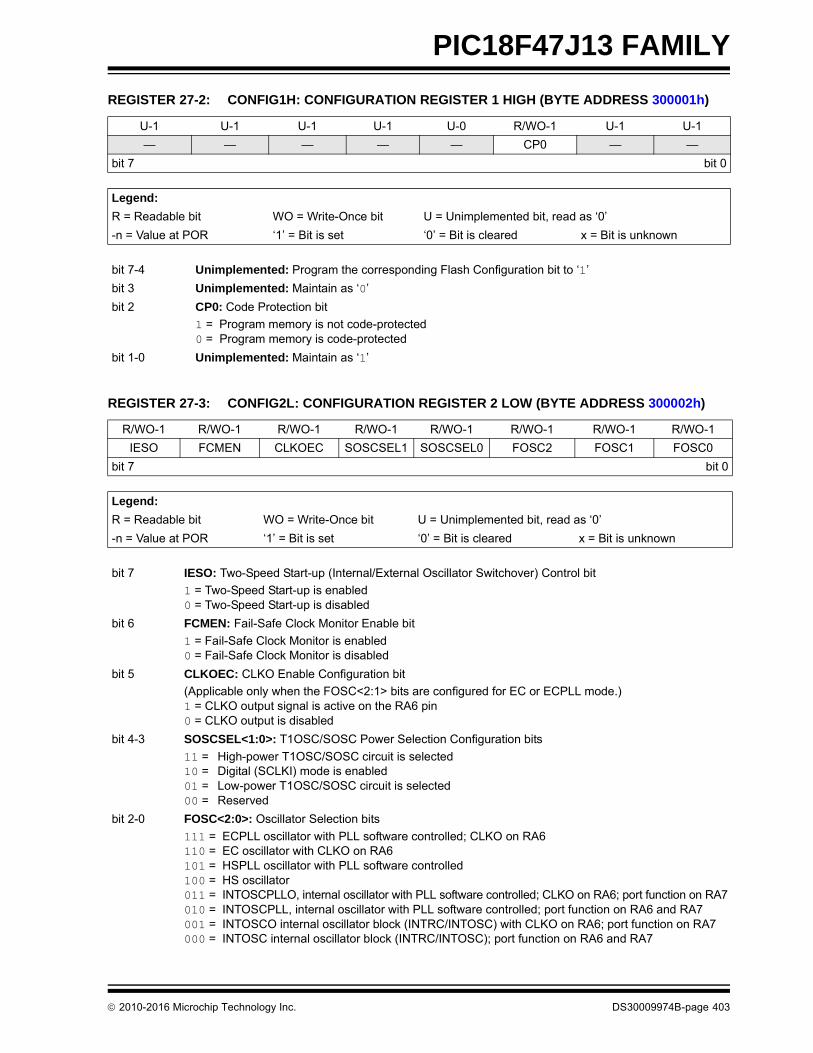
2010-2016 Microchip Technology Inc. DS30009974B-page 403
PIC18F47J13 FAMILY
REGISTER 27-2: CONFIG1H: CONFIGURATION REGISTER 1 HIGH (BYTE ADDRESS 300001h)
U-1 U-1 U-1 U-1 U-0 R/WO-1 U-1 U-1
— — — — — CP0 — —
bit 7 bit 0
Legend:
R = Readable bit WO = Write-Once bit U = Unimplemented bit, read as ‘0’
-n = Value at POR ‘1’ = Bit is set ‘0’ = Bit is cleared x = Bit is unknown
bit 7-4 Unimplemented: Program the corresponding Flash Configuration bit to ‘1’
bit 3 Unimplemented: Maintain as ‘0’
bit 2 CP0: Code Protection bit
1 = Program memory is not code-protected0 = Program memory is code-protected
bit 1-0 Unimplemented: Maintain as ‘1’
REGISTER 27-3: CONFIG2L: CONFIGURATION REGISTER 2 LOW (BYTE ADDRESS 300002h)
R/WO-1 R/WO-1 R/WO-1 R/WO-1 R/WO-1 R/WO-1 R/WO-1 R/WO-1
IESO FCMEN CLKOEC SOSCSEL1 SOSCSEL0 FOSC2 FOSC1 FOSC0
bit 7 bit 0
Legend:
R = Readable bit WO = Write-Once bit U = Unimplemented bit, read as ‘0’
-n = Value at POR ‘1’ = Bit is set ‘0’ = Bit is cleared x = Bit is unknown
bit 7 IESO: Two-Speed Start-up (Internal/External Oscillator Switchover) Control bit
1 = Two-Speed Start-up is enabled0 = Two-Speed Start-up is disabled
bit 6 FCMEN: Fail-Safe Clock Monitor Enable bit
1 = Fail-Safe Clock Monitor is enabled0 = Fail-Safe Clock Monitor is disabled
bit 5 CLKOEC: CLKO Enable Configuration bit
(Applicable only when the FOSC<2:1> bits are configured for EC or ECPLL mode.)1 = CLKO output signal is active on the RA6 pin0 = CLKO output is disabled
bit 4-3 SOSCSEL<1:0>: T1OSC/SOSC Power Selection Configuration bits
11 = High-power T1OSC/SOSC circuit is selected10 = Digital (SCLKI) mode is enabled01 = Low-power T1OSC/SOSC circuit is selected00 = Reserved
bit 2-0 FOSC<2:0>: Oscillator Selection bits
111 = ECPLL oscillator with PLL software controlled; CLKO on RA6110 = EC oscillator with CLKO on RA6101 = HSPLL oscillator with PLL software controlled100 = HS oscillator011 = INTOSCPLLO, internal oscillator with PLL software controlled; CLKO on RA6; port function on RA7010 = INTOSCPLL, internal oscillator with PLL software controlled; port function on RA6 and RA7001 = INTOSCO internal oscillator block (INTRC/INTOSC) with CLKO on RA6; port function on RA7000 = INTOSC internal oscillator block (INTRC/INTOSC); port function on RA6 and RA7

PIC18F47J13 FAMILY
DS30009974B-page 404 2010-2016 Microchip Technology Inc.
REGISTER 27-4: CONFIG2H: CONFIGURATION REGISTER 2 HIGH (BYTE ADDRESS 300003h)
U-1 U-1 U-1 U-1 R/WO-1 R/WO-1 R/WO-1 R/WO-1
— — — — WDTPS3 WDTPS2 WDTPS1 WDTPS0
bit 7 bit 0
Legend:
R = Readable bit WO = Write-Once bit U = Unimplemented bit, read as ‘0’
-n = Value at POR ‘1’ = Bit is set ‘0’ = Bit is cleared x = Bit is unknown
bit 7-4 Unimplemented: Program the corresponding Flash Configuration bit to ‘1’
bit 3-0 WDTPS<3:0>: Watchdog Timer Postscale Select bits
1111 = 1:32,7681110 = 1:16,3841101 = 1:8,1921100 = 1:4,0961011 = 1:2,0481010 = 1:1,0241001 = 1:5121000 = 1:2560111 = 1:1280110 = 1:640101 = 1:320100 = 1:160011 = 1:80010 = 1:40001 = 1:20000 = 1:1

2010-2016 Microchip Technology Inc. DS30009974B-page 405
PIC18F47J13 FAMILY
REGISTER 27-5: CONFIG3L: CONFIGURATION REGISTER 3 LOW (BYTE ADDRESS 300004h)
R/WO-1 R/WO-1 R/WO-1 R/WO-1 R/WO-1 R/WO-1 R/WO-1 R/WO-1
DSWDTPS3(1) DSWDTPS2(1) DSWDTPS1(1) DSWDTPS0(1) DSWDTEN(1) DSBOREN RTCOSC DSWDTOSC(1)
bit 7 bit 0
Legend:
R = Readable bit WO = Write-Once bit U = Unimplemented bit, read as ‘0’
-n = Value at POR ‘1’ = Bit is set ‘0’ = Bit is cleared x = Bit is unknown
bit 7-4 DSWDTPS<3:0>: Deep Sleep Watchdog Timer Postscale Select bits(1)
The DSWDT prescaler is 32. This creates an approximate base time unit of 1 ms.1111 = 1:2,147,483,648 (25.7 days)1110 = 1:536,870,912 (6.4 days)1101 = 1:134,217,728 (38.5 hours)1100 = 1:33,554,432 (9.6 hours)1011 = 1:8,388,608 (2.4 hours)1010 = 1:2,097,152 (36 minutes)1001 = 1:524,288 (9 minutes)1000 = 1:131,072 (135 seconds)0111 = 1:32,768 (34 seconds)0110 = 1:8,192 (8.5 seconds)0101 = 1:2,048 (2.1 seconds)0100 = 1:512 (528 ms)0011 = 1:128 (132 ms)0010 = 1:32 (33 ms)0001 = 1:8 (8.3 ms)0000 = 1:2 (2.1 ms)
bit 3 DSWDTEN: Deep Sleep Watchdog Timer Enable bit(1)
1 = DSWDT is enabled0 = DSWDT is disabled
bit 2 DSBOREN: “F” Device Deep Sleep BOR Enable bit, “LF” Device VDD BOR Enable bit
For “F” Devices:1 = VDD sensing BOR is enabled in Deep Sleep0 = VDD sensing BOR circuit is always disabled
For “LF” Devices:1 = VDD sensing BOR circuit is always enabled0 = VDD sensing BOR circuit is always disabled
bit 1 RTCOSC: RTCC Reference Clock Select bit
1 = RTCC uses T1OSC/T1CKI as the reference clock0 = RTCC uses INTRC as the reference clock
bit 0 DSWDTOSC: DSWDT Reference Clock Select bit(1)
1 = DSWDT uses INTRC as the reference clock0 = DSWDT uses T1OSC/T1CKI as the reference clock
Note 1: Functions are not available on “LF” devices.

PIC18F47J13 FAMILY
DS30009974B-page 406 2010-2016 Microchip Technology Inc.
REGISTER 27-6: CONFIG3H: CONFIGURATION REGISTER 3 HIGH (BYTE ADDRESS 300005h)
U-1 U-1 U-1 U-1 R/WO-1 R/WO-1 R/WO-1 R/WO-1
— — — — MSSPMSK PLLSEL ADCSEL IOL1WAY
bit 7 bit 0
Legend:
R = Readable bit WO = Write-Once bit U = Unimplemented bit, read as ‘0’
-n = Value at POR ‘1’ = Bit is set ‘0’ = Bit is cleared x = Bit is unknown
bit 7-4 Unimplemented: Program the corresponding Flash Configuration bit to ‘1’
bit 3 MSSPMSK: MSSP 7-Bit Address Masking Mode Enable bit
1 = 7-Bit Address Masking mode is enabled0 = 5-Bit Address Masking mode is enabled
bit 2 PLLSEL: PLL Circuit Selection bit
1 = 4x PLL circuit is selected0 = 96 MHz PLL circuit is selected
bit 1 ADCSEL: A/D Converter Mode bit
1 = 10-Bit Conversion mode is enabled0 = 12-Bit Conversion mode is enabled
bit 0 IOL1WAY: IOLOCK One-Way Set Enable bit
1 = IOLOCK bit (PPSCON<0>) can be set once, provided the unlock sequence has been completed;once set, the Peripheral Pin Select registers cannot be written to a second time
0 = IOLOCK bit (PPSCON<0>) can be set and cleared as needed, provided the unlock sequence hasbeen completed
REGISTER 27-7: CONFIG4L: CONFIGURATION REGISTER 4 LOW (BYTE ADDRESS 300006h)
R/WO-1 R/WO-1 R/WO-1 R/WO-1 R/WO-1 R/WO-1 R/WO-1 R/WO-1
WPCFG WPFP6 WPFP5 WPFP4 WPFP3 WPFP2 WPFP1 WPFP0
bit 7 bit 0
Legend:
R = Readable bit WO = Write-Once bit U = Unimplemented bit, read as ‘0’
-n = Value at POR ‘1’ = Bit is set ‘0’ = Bit is cleared x = Bit is unknown
bit 7 WPCFG: Write/Erase Protect Configuration Region Select bit (valid when WPDIS = 0)
1 = Configuration Words page is not erase/write-protected unless WPEND and WPFP<5:0> settingsinclude the Configuration Words page(1)
0 = Configuration Words page is erase/write-protected, regardless of WPEND and WPFP<5:0>(1)
bit 6-0 WPFP<6:0>: Write/Erase Protect Page Start/End Location bits
Used with the WPEND bit to define which pages in Flash will be erase/write-protected.
Note 1: The “Configuration Words page” contains the FCWs and is the last page of implemented Flash memory on a given device. Each page consists of 1,024 bytes. For example, on a device with 64 Kbytes of Flash, the first page is 0 and the last page (Configuration Words page) is 63 (3Fh).

2010-2016 Microchip Technology Inc. DS30009974B-page 407
PIC18F47J13 FAMILY
REGISTER 27-8: CONFIG4H: CONFIGURATION REGISTER 4 HIGH (BYTE ADDRESS 300007h)
U-1 U-1 U-1 U-1 U-0 U-0 R/WO-1 R/WO-1
— — — — — — WPEND WPDIS
bit 7 bit 0
Legend:
R = Readable bit WO = Write-Once bit U = Unimplemented bit, read as ‘0’
-n = Value at POR ‘1’ = Bit is set ‘0’ = Bit is cleared x = Bit is unknown
bit 7-4 Unimplemented: Program the corresponding Flash Configuration bit to ‘1’
bit 3-2 Unimplemented: Read as ‘0’
bit 1 WPEND: Write-Protect Disable bit
1 = Flash pages, WPFP<6:0> to (Configuration Words page), are erase/write-protected0 = Flash pages 0 to WPFP<6:0> are erase/write-protected
bit 0 WPDIS: Write-Protect Disable bit
1 = WPFP<5:0>, WPEND and WPCFG bits are ignored; all Flash memory may be erased or written0 = WPFP<5:0>, WPEND and WPCFG bits are enabled; erase/write-protect is active for the selected
region(s)
REGISTER 27-9: DEVID1: DEVICE ID REGISTER 1 FOR PIC18F47J13 FAMILY DEVICES (BYTE ADDRESS 3FFFFEh)
R R R R R R R R
DEV2 DEV1 DEV0 REV4 REV3 REV2 REV1 REV0
bit 7 bit 0
Legend:
R = Readable bit W = Writable bit U = Unimplemented bit, read as ‘0’
-n = Value at POR ‘1’ = Bit is set ‘0’ = Bit is cleared x = Bit is unknown
bit 7-5 DEV<2:0>: Device ID bits
These bits are used with DEV<10:3> bits in Device ID Register 2 to identify the part number. See Register 27-10.
bit 4-0 REV<4:0>: Revision ID bits
These bits are used to indicate the device revision.

PIC18F47J13 FAMILY
DS30009974B-page 408 2010-2016 Microchip Technology Inc.
REGISTER 27-10: DEVID2: DEVICE ID REGISTER 2 FOR PIC18F47J13 FAMILY DEVICES (BYTE ADDRESS 3FFFFFh)
R R R R R R R R
DEV10 DEV9 DEV8 DEV7 DEV6 DEV5 DEV4 DEV3
bit 7 bit 0
Legend:
R = Readable bit W = Writable bit U = Unimplemented bit, read as ‘0’
-n = Value at POR ‘1’ = Bit is set ‘0’ = Bit is cleared x = Bit is unknown
bit 7-0 DEV<10:3>: Device ID bits
These bits are used with the DEV<2:0> bits in the Device ID Register 1 to identify the part number.
DEV<10:3>(DEVID2<7:0>)
DEV<2:0>(DEVID1<7:5>)
Device
0101 1001 111 PIC18F47J13
0101 1001 101 PIC18F46J13
0101 1001 011 PIC18F27J13
0101 1001 001 PIC18F26J13
0101 1011 111 PIC18LF47J13
0101 1011 101 PIC18LF46J13
0101 1011 011 PIC18LF27J13
0101 1011 001 PIC18LF26J13

2010-2016 Microchip Technology Inc. DS30009974B-page 409
PIC18F47J13 FAMILY
27.2 Watchdog Timer (WDT)
PIC18F47J13 Family devices have both a conventionalWDT circuit and a dedicated, Deep Sleep capableWatchdog Timer. When enabled, the conventionalWDT operates in normal Run, Idle and Sleep modes.This data sheet section describes the conventionalWDT circuit.
The dedicated, Deep Sleep capable WDT can only beenabled in Deep Sleep mode. This timer is described inSection 4.6.4 “Deep Sleep Watchdog Timer(DSWDT)”.
The conventional WDT is driven by the INTRCoscillator. When the WDT is enabled, the clock sourceis also enabled. The nominal WDT period is 4 ms andhas the same stability as the INTRC oscillator.
The 4 ms period of the WDT is multiplied by a 16-bitpostscaler. Any output of the WDT postscaler isselected by a multiplexer, controlled by the WDTPS bitsin Configuration Register 2H. Available periods rangefrom about 4 ms to 135 seconds (2.25 minutesdepending on voltage, temperature and WDTpostscaler). The WDT and postscaler are cleared
whenever a SLEEP or CLRWDT instruction is executed,or a clock failure (primary or Timer1 oscillator) hasoccurred.
27.2.1 CONTROL REGISTER
The WDTCON register (Register 27-11) is a readableand writable register. The SWDTEN bit enables or dis-ables WDT operation. This allows software to overridethe WDTEN Configuration bit and enable the WDT onlyif it has been disabled by the Configuration bit.
LVDSTAT is a read-only status bit that is continuouslyupdated and provides information about the currentlevel of VDDCORE. This bit is only valid when the on-chipvoltage regulator is enabled.
FIGURE 27-1: WDT BLOCK DIAGRAM
Note 1: The CLRWDT and SLEEP instructionsclear the WDT and postscaler countswhen executed.
2: When a CLRWDT instruction is executed,the postscaler count will be cleared.
INTRC Oscillator
WDT
Wake-up from
Reset
WDT
WDT Counter
Programmable Postscaler1:1 to 1:32,768
Enable WDT
WDTPS<3:0>
SWDTEN
CLRWDT
4
Power-Managed
ResetAll Device Resets
SLEEP
INTRC Control
128
Modes

PIC18F47J13 FAMILY
DS30009974B-page 410 2010-2016 Microchip Technology Inc.
TABLE 27-3: SUMMARY OF WATCHDOG TIMER REGISTERS
REGISTER 27-11: WDTCON: WATCHDOG TIMER CONTROL REGISTER (ACCESS FC0h)
R/W-1 R-x R-x R/W-0 R-0 R/W-0 R/W-0 R/W-0
REGSLP LVDSTAT(2) ULPLVL VBGOE DS(2) ULPEN ULPSINK SWDTEN(1)
bit 7 bit 0
Legend:
R = Readable bit W = Writable bit U = Unimplemented bit, read as ‘0’
-n = Value at POR ‘1’ = Bit is set ‘0’ = Bit is cleared x = Bit is unknown
bit 7 REGSLP: Voltage Regulator Low-Power Operation Enable bit
1 = On-chip regulator enters low-power operation when device enters Sleep mode0 = On-chip regulator is active even in Sleep mode
bit 6 LVDSTAT: Low-Voltage Detect Status bit(2)
1 = VDDCORE > 2.45V nominal0 = VDDCORE < 2.45V nominal
bit 5 ULPLVL: Ultra Low-Power Wake-up Output bit (not valid unless ULPEN = 1)
1 = Voltage on RA0 > ~0.5V0 = Voltage on RA0 < ~0.5V
bit 4 VBGOE: Band Gap Reference Voltage (VBG) Output Enable bit
1 = Band gap reference output is enabled on the RA1 pin0 = Band gap reference output is disabled
bit 3 DS: Deep Sleep Wake-up Status bit (used in conjunction with RCON, POR and BOR bits to determine Reset source)(2)
1 = If the last exit from Reset was caused by a normal wake-up from Deep Sleep0 = If the last exit from Reset was not due to a wake-up from Deep Sleep
bit 2 ULPEN: Ultra Low-Power Wake-up Module Enable bit
1 = Ultra low-power wake-up module is enabled; ULPLVL bit indicates the comparator output0 = Ultra low-power wake-up module is disabled
bit 1 ULPSINK: Ultra Low-Power Wake-up Current Sink Enable bit
1 = Ultra low-power wake-up current sink is enabled (if ULPEN = 1)0 = Ultra low-power wake-up current sink is disabled
bit 0 SWDTEN: Software Controlled Watchdog Timer Enable bit(1)
1 = Watchdog Timer is on0 = Watchdog Timer is off
Note 1: This bit has no effect if the Configuration bit, WDTEN, is enabled.
2: Not available on devices where the on-chip voltage regulator is disabled (“LF” devices).
Name Bit 7 Bit 6 Bit 5 Bit 4 Bit 3 Bit 2 Bit 1 Bit 0
RCON IPEN — CM RI TO PD POR BOR
WDTCON REGSLP LVDSTAT ULPLVL VBGOE DS ULPEN ULPSINK SWDTEN
Legend: — = unimplemented, read as ‘0’. Shaded cells are not used by the Watchdog Timer.

2010-2016 Microchip Technology Inc. DS30009974B-page 411
PIC18F47J13 FAMILY
27.3 On-Chip Voltage Regulator
The digital core logic of the PIC18F47J13 Familydevices is designed on an advanced manufacturingprocess, which requires 2.0V to 2.7V. The digital corelogic obtains power from the VDDCORE/VCAP powersupply pin.
However, in many applications it may be inconvenientto run the I/O pins at the same core logic voltage, as itwould restrict the ability of the device to interface withother higher voltage devices, such as those run at anominal 3.3V. Therefore, all PIC18F47J13 Familydevices implement a dual power supply rail topology.The core logic obtains power from the VDDCORE/VCAP
pin, while the general purpose I/O pins obtain powerfrom the VDD pin of the microcontroller, which may besupplied with a voltage between 2.15V to 3.6V (“F”device) or 2.0V to 3.6V (“LF” device).
This dual supply topology allows the microcontroller tointerface with standard 3.3V logic devices, while runningthe core logic at a lower voltage of nominally 2.5V.
In order to make the microcontroller more convenient touse, an integrated 2.5V low dropout, low quiescentcurrent linear regulator has been integrated on the dieinside PIC18F47J13 Family devices. This regulator isdesigned specifically to supply the core logic of thedevice. It allows PIC18F47J13 Family devices toeffectively run from a single power supply rail, withoutthe need for external regulators.
The on-chip voltage regulator is always enabled on “F”devices. The VDDCORE/VCAP pin simultaneously servesas the regulator output pin and the core logic supplypower input pin. A capacitor should be connected to theVDDCORE/VCAP pin to ground and is necessary for regu-lator stability. For example connections for PIC18F andPIC18LF devices, see Figure 27-2.
On “LF” devices, the on-chip regulator is alwaysdisabled. This allows the device to save a small amountof quiescent current consumption, which may be
advantageous in some types of applications, such asthose which will entirely be running at a nominal 2.5V.On “LF” devices, the VDDCORE/VCAP pin still serves asthe core logic power supply input pin, and therefore,must be connected to a 2.0V to 2.7V supply rail at theapplication circuit board level. On these devices, theI/O pins may still optionally be supplied with a voltagebetween 2.0V to 3.6V, provided that VDD is alwaysgreater than, or equal to, VDDCORE/VCAP. For exampleconnections for PIC18F and PIC18LF devices, seeFigure 27-2.
The specifications for core voltage and capacitanceare listed in Section 30.3 “DC Characteristics:PIC18F47J13 Family (Industrial)”.
27.3.1 VOLTAGE REGULATOR TRACKING MODE AND LOW-VOLTAGE DETECTION
On “F” devices, the on-chip regulator provides a con-stant voltage of 2.5V nominal to the digital core logic.The regulator can provide this level from a VDD of about2.5V, all the way up to the device’s VDDMAX. It does nothave the capability to boost VDD levels below 2.5V.When the VDD supply input voltage drops too low toregulate 2.5V, the regulator enters Tracking mode. InTracking mode, the regulator output follows VDD, with atypical voltage drop of 100 mV or less.
The on-chip regulator includes a simple Low-VoltageDetect (LVD) circuit. This circuit is separate andindependent of the High/Low-Voltage Detect (HLVD)module described in Section 25.0 “High/Low VoltageDetect (HLVD)”. The on-chip regulator LVD circuit con-tinuously monitors the VDDCORE voltage level andupdates the LVDSTAT bit in the WDTCON register. TheLVD detect threshold is set slightly below the normalregulation set point of the on-chip regulator.
Application firmware may optionally poll the LVDSTATbit to determine when it is safe to run at the maximumrated frequency, so as not to inadvertently violate thevoltage versus frequency requirements provided byFigure 30-1.
The VDDCORE monitoring LVD circuit is only activewhen the on-chip regulator is enabled. On “LF”devices, the Analog-to-Digital Converter and the HLVDmodule can still be used to provide firmware with VDD
and VDDCORE voltage level information.
Note 1: The on-chip voltage regulator is onlyavailable in parts designated with an “F”,such as PIC18F26J13. The on-chipregulator is disabled on devices with “LF”in their part number.
2: The VDDCORE/VCAP pin must never beleft floating. On “F” devices, it must beconnected to a capacitor of size, CEFC, toground. On “LF” devices, VDDCORE/VCAP
must be connected to a power supplysource between 2.0V and 2.7V.
Note: In parts designated with an “LF”, such asPIC18LF47J13, VDDCORE must neverexceed VDD.

PIC18F47J13 FAMILY
DS30009974B-page 412 2010-2016 Microchip Technology Inc.
FIGURE 27-2: CONNECTIONS FOR THE ON-CHIP REGULATOR
27.3.2 ON-CHIP REGULATOR AND BOR
When the on-chip regulator is enabled, PIC18F47J13Family devices also have a simple brown-out capabil-ity. If the voltage supplied to the regulator is inadequateto maintain a minimum output level, the regulator Resetcircuitry will generate a Brown-out Reset (BOR). Thisevent is captured by the BOR flag bit (RCON<0>).
The operation of the BOR is described in more detail inSection 5.4 “Brown-out Reset (BOR)” andSection 5.4.1 “Detecting BOR”. The brown-out voltagelevels are specific in Section 30.1 “DC Characteristics:Supply Voltage PIC18F47J13 Family (Industrial)”.
27.3.3 POWER-UP REQUIREMENTS
The on-chip regulator is designed to meet the power-uprequirements for the device. If the application does notuse the regulator, then strict power-up conditions mustbe adhered to. While powering up, VDDCORE should notexceed VDD by 0.3 volts.
27.3.4 OPERATION IN SLEEP MODE
When enabled, the on-chip regulator always consumesa small incremental amount of current over IDD. Thisincludes when the device is in Sleep mode, eventhough the core digital logic does not require muchpower. To provide additional savings in applicationswhere power resources are critical, the regulator canbe configured to automatically enter a lower quiescentdraw Standby mode whenever the device goes intoSleep mode. This feature is controlled by the REGSLPbit (WDTCON<7>, Register 27-11). If this bit is setupon entry into Sleep mode, the regulator will transitioninto a lower power state. In this state, the regulator stillprovides a regulated output voltage necessary tomaintain SRAM state information, but consumes lessquiescent current.
Substantial Sleep mode power savings can beobtained by setting the REGSLP bit, but devicewake-up time will increase in order to insure theregulator has enough time to stabilize.
VDD
VDDCORE/VCAP
VSS
3.3V2.5V
VDD
VDDCORE/VCAP
VSSCF
3.3V
OR
VDD
VDDCORE/VCAP
VSS
2.5V
PIC18FXXJ13 Devices (Regulator Enabled):
PIC18LFXXJ13 Devices (Regulator Disabled):
PIC18FXXJ13
PIC18LFXXJ13
PIC18LFXXJ13

2010-2016 Microchip Technology Inc. DS30009974B-page 413
PIC18F47J13 FAMILY
27.4 Two-Speed Start-up
The Two-Speed Start-up feature helps to minimize thelatency period, from oscillator start-up to code execu-tion, by allowing the microcontroller to use the INTRCoscillator as a clock source until the primary clocksource is available. It is enabled by setting the IESOConfiguration bit.
Two-Speed Start-up should be enabled only if theprimary oscillator mode is HS or HSPLL(Crystal-Based) modes. Since the EC and ECPLLmodes do not require an Oscillator Start-up Timer(OST) delay, Two-Speed Start-up should be disabled.
When enabled, Resets and wake-ups from Sleep modecause the device to configure itself to run from the inter-nal oscillator block as the clock source, following thetime-out of the Power-up Timer after a Power-on Resetis enabled. This allows almost immediate codeexecution while the primary oscillator starts and theOST is running. Once the OST times out, the deviceautomatically switches to PRI_RUN mode.
In all other power-managed modes, Two-SpeedStart-up is not used. The device will be clocked by thecurrently selected clock source until the primary clocksource becomes available. The setting of the IESO bitis ignored.
FIGURE 27-3: TIMING TRANSITION FOR TWO-SPEED START-UP (INTRC TO HSPLL)
27.4.1 SPECIAL CONSIDERATIONS FOR USING TWO-SPEED START-UP
While using the INTRC oscillator in Two-SpeedStart-up, the device still obeys the normal commandsequences for entering power-managed modes,including serial SLEEP instructions (refer toSection 4.1.4 “Multiple Sleep Commands”). Inpractice, this means that user code can change theSCS<1:0> bit settings or issue SLEEP instructionsbefore the OST times out. This would allow an applica-tion to briefly wake-up, perform routine “housekeeping”tasks and return to Sleep before the device starts tooperate from the primary oscillator.
User code can also check if the primary clock source iscurrently providing the device clocking by checking thestatus of the OSTS bit (OSCCON<3>). If the bit is set,the primary oscillator is providing the clock. Otherwise,the internal oscillator block is providing the clock duringwake-up from Reset or Sleep mode.
27.5 Fail-Safe Clock Monitor
The Fail-Safe Clock Monitor (FSCM) allows the micro-controller to continue operation in the event of an externaloscillator failure by automatically switching the deviceclock to the internal oscillator block. The FSCM functionis enabled by setting the FCMEN Configuration bit.
When FSCM is enabled, the INTRC oscillator runs atall times to monitor clocks to peripherals and provide abackup clock in the event of a clock failure. Clockmonitoring (shown in Figure 27-4) is accomplished bycreating a sample clock signal, which is the INTRC out-put divided by 64. This allows ample time betweenFSCM sample clocks for a peripheral clock edge tooccur. The peripheral device clock and the sampleclock are presented as inputs to the clock monitor latch.The clock monitor is set on the falling edge of thedevice clock source but cleared on the rising edge ofthe sample clock.
Q1 Q3 Q4
OSC1
Peripheral
Program PC PC + 2
INTRC
PLL Clock
Q1
PC + 6
Q2
Output
Q3 Q4 Q1
CPU Clock
PC + 4
Clock
Counter
Q2 Q2 Q3
Note 1: TOST = 1024 TOSC; TPLL = 2 ms (approx). These intervals are not shown to scale.
Wake from Interrupt Event
TPLL(1)
1 2 n-1 n
Clock
OSTS bit Set
Transition
TOST(1)

PIC18F47J13 FAMILY
DS30009974B-page 414 2010-2016 Microchip Technology Inc.
FIGURE 27-4: FSCM BLOCK DIAGRAM
Clock failure is tested for on the falling edge of thesample clock. If a sample clock falling edge occurswhile the clock monitor is still set, and a clock failurehas been detected (Figure 27-5), the following results:
• The FSCM generates an oscillator fail interrupt by setting bit, OSCFIF (PIR2<7>);
• The device clock source is switched to the internal oscillator block (OSCCON is not updated to show the current clock source – this is the fail-safe condition); and
• The WDT is reset.
During switchover, the postscaler frequency from theinternal oscillator block may not be sufficiently stablefor timing-sensitive applications. In these cases, it may
be desirable to select another clock configuration andenter an alternate power-managed mode. This can bedone to attempt a partial recovery or execute acontrolled shutdown. See Section 4.1.4 “MultipleSleep Commands” and Section 27.4.1 “SpecialConsiderations For Using Two-speed Start-up” formore details.
The FSCM will detect failures of the primary or secondaryclock sources only. If the internal oscillator block fails, nofailure would be detected, nor would any action bepossible.
27.5.1 FSCM AND THE WATCHDOG TIMER
Both the FSCM and the WDT are clocked by theINTRC oscillator. Since the WDT operates with aseparate divider and counter, disabling the WDT hasno effect on the operation of the INTRC oscillator whenthe FSCM is enabled.
As already noted, the clock source is switched to theINTRC clock when a clock failure is detected; this maymean a substantial change in the speed of code execu-tion. If the WDT is enabled with a small prescale value,a decrease in clock speed allows a WDT time-out tooccur and a subsequent device Reset. For this reason,Fail-Safe Clock Monitor events also reset the WDT andpostscaler, allowing it to start timing from when execu-tion speed was changed and decreasing the likelihoodof an erroneous time-out.
FIGURE 27-5: FSCM TIMING DIAGRAM
Peripheral
INTRC÷ 64
S
C
Q
(32 s) 488 Hz(2.048 ms)
Clock MonitorLatch
(edge-triggered)
ClockFailure
Detected
Source
Clock
Q
OSCFIF
Clock Monitor
DeviceClock
Output
Sample Clock
FailureDetected
OscillatorFailure
Note: The device clock is normally at a much higher frequency than the sample clock. The relative frequencies inthis example have been chosen for clarity.
Output (Q)
Clock Monitor Test Clock Monitor Test Clock Monitor Test

2010-2016 Microchip Technology Inc. DS30009974B-page 415
PIC18F47J13 FAMILY
27.5.2 EXITING FAIL-SAFE OPERATION
The Fail-Safe Clock Monitor condition is terminated byeither a device Reset or by entering a power-managedmode. On Reset, the controller starts the primary clocksource specified in Configuration Register 2H (with anyrequired start-up delays that are required for the oscil-lator mode, such as the OST or PLL timer). The INTRCoscillator provides the device clock until the primaryclock source becomes ready (similar to a Two-SpeedStart-up). The clock source is then switched to theprimary clock (indicated by the OSTS bit in theOSCCON register becoming set). The FSCM thenresumes monitoring the peripheral clock.
The primary clock source may never become readyduring start-up. In this case, operation is clocked by theINTRC oscillator. The OSCCON register will remain inits Reset state until a power-managed mode is entered.
27.5.3 FSCM INTERRUPTS IN POWER-MANAGED MODES
By entering a power-managed mode, the clockmultiplexer selects the clock source selected by theOSCCON register. FSCM of the power-managed clocksource resumes in the power-managed mode.
If an oscillator failure occurs during power-managedoperation, the subsequent events depend on whetheror not the oscillator failure interrupt is enabled. Ifenabled (OSCFIF = 1), code execution will be clockedby the INTRC multiplexer. An automatic transition backto the failed clock source will not occur.
If the interrupt is disabled, subsequent interrupts whilein Idle mode will cause the CPU to begin executinginstructions while being clocked by the INTRC source.
27.5.4 POR OR WAKE-UP FROM SLEEP
The FSCM is designed to detect oscillator failure at anypoint after the device has exited Power-on Reset (POR)or low-power Sleep mode. When the primary deviceclock is either the EC or INTRC modes, monitoring canbegin immediately following these events.
For HS or HSPLL modes, the situation is somewhatdifferent. Since the oscillator may require a start-uptime considerably longer than the FSCM sample clocktime, a false clock failure may be detected. To preventthis, the internal oscillator block is automatically config-ured as the device clock and functions until the primaryclock is stable (the OST and PLL timers have timed
out). This is identical to Two-Speed Start-up mode.Once the primary clock is stable, the INTRC returns toits role as the FSCM source.
As noted in Section 27.4.1 “Special ConsiderationsFor Using Two-speed Start-up”, it is also possible toselect another clock configuration and enter an alternatepower-managed mode while waiting for the primaryclock to become stable. When the new power-managedmode is selected, the primary clock is disabled.
27.6 Program Verification and Code Protection
For all devices in the PIC18F47J13 Family of devices,the on-chip program memory space is treated as asingle block. Code protection for this block is controlledby one Configuration bit, CP0. This bit inhibits externalreads and writes to the program memory space. It hasno direct effect in normal execution mode.
27.6.1 CONFIGURATION REGISTER PROTECTION
The Configuration registers are protected againstuntoward changes or reads in two ways. The primaryprotection is the write-once feature of the Configurationbits, which prevents reconfiguration once the bit hasbeen programmed during a power cycle. To safeguardagainst unpredictable events, Configuration bitchanges resulting from individual cell level disruptions(such as ESD events) will cause a parity error andtrigger a device Reset. This is seen by the user as aConfiguration Mismatch (CM) Reset.
The data for the Configuration registers is derived fromthe FCW in program memory. When the CP0 bit is set,the source data for device configuration is alsoprotected as a consequence.
Note: The same logic that prevents falseoscillator failure interrupts on POR, orwake-up from Sleep, will also prevent thedetection of the oscillator’s failure to startat all following these events. This can beavoided by monitoring the OSTS bit andusing a timing routine to determine if theoscillator is taking too long to start. Evenso, no oscillator failure interrupt will beflagged.

PIC18F47J13 FAMILY
DS30009974B-page 416 2010-2016 Microchip Technology Inc.
27.7 In-Circuit Serial Programming™ (ICSP™)
PIC18F47J13 Family microcontrollers can be seriallyprogrammed while in the end application circuit. This issimply done with two lines for clock and data, and threeother lines for power, ground and the programmingvoltage. This allows customers to manufacture boardswith unprogrammed devices and then program themicrocontroller just before shipping the product. Thisalso allows the most recent firmware or a customfirmware to be programmed.
27.8 In-Circuit Debugger
When the DEBUG Configuration bit is programmed toa ‘0’, the In-Circuit Debugger functionality is enabled.This function allows simple debugging functions whenused with MPLAB® IDE. When the microcontroller hasthis feature enabled, some resources are not availablefor general use.
Table 27-4 lists the resources required by thebackground debugger.
TABLE 27-4: DEBUGGER RESOURCES
I/O Pins: RB6, RB7
Stack: TOSx registers reserved.

2010-2016 Microchip Technology Inc. DS30009974B-page 417
PIC18F47J13 FAMILY
28.0 INSTRUCTION SET SUMMARY
The PIC18F47J13 Family of devices incorporate thestandard set of 75 PIC18 core instructions, as well asan extended set of 8 new instructions for the optimiza-tion of code that is recursive or that utilizes a softwarestack. The extended set is discussed later in thissection.
28.1 Standard Instruction Set
The standard PIC18 MCU instruction set adds manyenhancements to the previous PIC® MCU instructionsets, while maintaining an easy migration from thesePIC MCU instruction sets. Most instructions are asingle program memory word (16 bits), but there arefour instructions that require two program memorylocations.
Each single-word instruction is a 16-bit word dividedinto an opcode, which specifies the instruction type andone or more operands, which further specify theoperation of the instruction.
The instruction set is highly orthogonal and is groupedinto four basic categories:
• Byte-oriented operations
• Bit-oriented operations
• Literal operations
• Control operations
The PIC18 instruction set summary in Table 28-2 listsbyte-oriented, bit-oriented, literal and controloperations. Table 28-1 shows the opcode fielddescriptions.
Most byte-oriented instructions have three operands:
1. The file register (specified by ‘f’)
2. The destination of the result (specified by ‘d’)
3. The accessed memory (specified by ‘a’)
The file register designator, ‘f’, specifies which fileregister is to be used by the instruction. The destinationdesignator, ‘d’, specifies where the result of theoperation is to be placed. If ‘d’ is zero, the result isplaced in the WREG register. If ‘d’ is one, the result isplaced in the file register specified in the instruction.
All bit-oriented instructions have three operands:
1. The file register (specified by ‘f’)
2. The bit in the file register (specified by ‘b’)
3. The accessed memory (specified by ‘a’)
The bit field designator, ‘b’, selects the number of the bitaffected by the operation, while the file register desig-nator, ‘f’, represents the number of the file in which thebit is located.
The literal instructions may use some of the followingoperands:
• A literal value to be loaded into a file register (specified by ‘k’)
• The desired FSR register to load the literal value into (specified by ‘f’)
• No operand required (specified by ‘—’)
The control instructions may use some of the followingoperands:
• A program memory address (specified by ‘n’)
• The mode of the CALL or RETURN instructions (specified by ‘s’)
• The mode of the table read and table write instructions (specified by ‘m’)
• No operand required (specified by ‘—’)
All instructions are a single word, except for fourdouble-word instructions. These instructions weremade double-word to contain the required informationin 32 bits. In the second word, the 4 MSbs are ‘1’s. Ifthis second word is executed as an instruction (byitself), it will execute as a NOP.
All single-word instructions are executed in a singleinstruction cycle, unless a conditional test is true or theprogram counter is changed as a result of the instruc-tion. In these cases, the execution takes two instructioncycles with the additional instruction cycle(s) executedas a NOP.
The double-word instructions execute in two instructioncycles.
One instruction cycle consists of four oscillator periods.Thus, for an oscillator frequency of 4 MHz, the normalinstruction execution time is 1 s. If a conditional test istrue, or the program counter is changed as a result ofan instruction, the instruction execution time is 2 s.Two-word branch instructions (if true) would take 3 s.
Figure 28-1 shows the general formats that the instruc-tions can have. All examples use the convention ‘nnh’to represent a hexadecimal number.
The Instruction Set Summary, shown in Table 28-2,lists the standard instructions recognized by theMicrochip MPASMTM Assembler.
Section 28.1.1 “Standard Instruction Set” providesa description of each instruction.

PIC18F47J13 FAMILY
DS30009974B-page 418 2010-2016 Microchip Technology Inc.
TABLE 28-1: OPCODE FIELD DESCRIPTIONS
Field Description
a RAM Access bit:a = 0: RAM location in Access RAM (BSR register is ignored)a = 1: RAM bank is specified by BSR register
bbb Bit address within an 8-bit file register (0 to 7).
BSR Bank Select Register. Used to select the current RAM bank.
C, DC, Z, OV, N ALU Status bits: Carry, Digit Carry, Zero, Overflow, Negative.
d Destination Select bit:d = 0: store result in WREGd = 1: store result in file register f
dest Destination: either the WREG register or the specified register file location.
f 8-bit Register file address (00h to FFh), or 2-bit FSR designator (0h to 3h).
fs 12-bit Register file address (000h to FFFh). This is the source address.
fd 12-bit Register file address (000h to FFFh). This is the destination address.
GIE Global Interrupt Enable bit.
k Literal field, constant data or label (may be either an 8-bit, 12-bit or a 20-bit value).
label Label name.
mm The mode of the TBLPTR register for the table read and table write instructions.Only used with table read and table write instructions:
* No change to register (such as TBLPTR with table reads and writes)
*+ Post-Increment register (such as TBLPTR with table reads and writes)
*- Post-Decrement register (such as TBLPTR with table reads and writes)
+* Pre-Increment register (such as TBLPTR with table reads and writes)
n The relative address (2’s complement number) for relative branch instructions or the direct address for Call/Branch and Return instructions.
PC Program Counter.
PCL Program Counter Low Byte.
PCH Program Counter High Byte.
PCLATH Program Counter High Byte Latch.
PCLATU Program Counter Upper Byte Latch.
PD Power-Down bit.
PRODH Product of Multiply High Byte.
PRODL Product of Multiply Low Byte.
s Fast Call/Return Mode Select bit:s = 0: do not update into/from shadow registerss = 1: certain registers loaded into/from shadow registers (Fast mode)
TBLPTR 21-bit Table Pointer (points to a program memory location).
TABLAT 8-bit Table Latch.
TO Time-out bit.
TOS Top-of-Stack.
u Unused or Unchanged.
WDT Watchdog Timer.
WREG Working register (accumulator).
x Don’t care (‘0’ or ‘1’). The assembler will generate code with x = 0. It is the recommended form of use for compatibility with all Microchip software tools.
zs 7-bit offset value for Indirect Addressing of register files (source).
zd 7-bit offset value for Indirect Addressing of register files (destination).
Optional argument.
[text] Indicates an Indexed Address.
(text) The contents of text.
[expr]<n> Specifies bit n of the register indicated by the pointer expr.
Assigned to.
< > Register bit field.
In the set of.
italics User-defined term (font is Courier New).

2010-2016 Microchip Technology Inc. DS30009974B-page 419
PIC18F47J13 FAMILY
FIGURE 28-1: GENERAL FORMAT FOR INSTRUCTIONS
Byte-oriented file register operations
15 10 9 8 7 0
d = 0 for result destination to be WREG register
OPCODE d a f (FILE #)
d = 1 for result destination to be file register (f)a = 0 to force Access Bank
Bit-oriented file register operations
15 12 11 9 8 7 0
OPCODE b (BIT #) a f (FILE #)
b = 3-bit position of bit in file register (f)
Literal operations
15 8 7 0
OPCODE k (literal)
k = 8-bit immediate value
Byte to Byte move operations (2-word)
15 12 11 0
OPCODE f (Source FILE #)
CALL, GOTO and Branch operations
15 8 7 0
OPCODE n<7:0> (literal)
n = 20-bit immediate value
a = 1 for BSR to select bankf = 8-bit file register address
a = 0 to force Access Banka = 1 for BSR to select bankf = 8-bit file register address
15 12 11 0
1111 n<19:8> (literal)
15 12 11 0
1111 f (Destination FILE #)
f = 12-bit file register address
Control operations
Example Instruction
ADDWF MYREG, W, B
MOVFF MYREG1, MYREG2
BSF MYREG, bit, B
MOVLW 7Fh
GOTO Label
15 8 7 0
OPCODE S n<7:0> (literal)
15 12 11 0
1111 n<19:8> (literal)
CALL MYFUNC
15 11 10 0
OPCODE n<10:0> (literal)
S = Fast bit
BRA MYFUNC
15 8 7 0
OPCODE n<7:0> (literal) BC MYFUNC

PIC18F47J13 FAMILY
DS30009974B-page 420 2010-2016 Microchip Technology Inc.
TABLE 28-2: PIC18F47J13 FAMILY INSTRUCTION SET
Mnemonic,Operands
Description Cycles16-Bit Instruction Word Status
AffectedNotes
MSb LSb
BYTE-ORIENTED OPERATIONS
ADDWFADDWFCANDWFCLRFCOMFCPFSEQCPFSGTCPFSLTDECFDECFSZDCFSNZINCFINCFSZINFSNZIORWFMOVFMOVFF
MOVWFMULWFNEGFRLCFRLNCFRRCFRRNCFSETFSUBFWB
SUBWFSUBWFB
SWAPFTSTFSZXORWF
f, d, af, d, af, d, af, af, d, af, af, af, af, d, af, d, af, d, af, d, af, d, af, d, af, d, af, d, afs, fd
f, af, af, af, d, af, d, af, d, af, d, af, af, d, a
f, d, af, d, a
f, d, af, af, d, a
Add WREG and fAdd WREG and Carry bit to fAND WREG with fClear fComplement fCompare f with WREG, Skip =Compare f with WREG, Skip >Compare f with WREG, Skip <Decrement fDecrement f, Skip if 0Decrement f, Skip if Not 0Increment fIncrement f, Skip if 0Increment f, Skip if Not 0Inclusive OR WREG with fMove fMove fs (source) to 1st word
fd (destination) 2nd wordMove WREG to fMultiply WREG with fNegate fRotate Left f through CarryRotate Left f (No Carry)Rotate Right f through CarryRotate Right f (No Carry)Set fSubtract f from WREG with Borrow Subtract WREG from fSubtract WREG from f with BorrowSwap Nibbles in fTest f, Skip if 0Exclusive OR WREG with f
111111 (2 or 3)1 (2 or 3)1 (2 or 3)11 (2 or 3)1 (2 or 3)11 (2 or 3)1 (2 or 3)112
111111111
11
11 (2 or 3)1
001000100001011000010110011001100000001001000010001101000001010111001111011000000110001101000011010001100101
01010101
001101100001
01da00da01da101a11da001a010a000a01da11da11da10da11da10da00da00daffffffff111a001a110a01da01da00da00da100a01da
11da10da
10da011a10da
ffffffffffffffffffffffffffffffffffffffffffffffffffffffffffffffffffffffffffffffffffffffffffffffffffffffffffff
ffffffff
ffffffffffff
ffffffffffffffffffffffffffffffffffffffffffffffffffffffffffffffffffffffffffffffffffffffffffffffffffffffffffff
ffffffff
ffffffffffff
C, DC, Z, OV, NC, DC, Z, OV, NZ, NZZ, NNoneNoneNoneC, DC, Z, OV, NNoneNoneC, DC, Z, OV, NNoneNoneZ, NZ, NNone
NoneNoneC, DC, Z, OV, NC, Z, NZ, NC, Z, NZ, NNoneC, DC, Z, OV, N
C, DC, Z, OV, NC, DC, Z, OV, N
NoneNoneZ, N
1, 21, 21,221, 2441, 21, 2, 3, 41, 2, 3, 41, 21, 2, 3, 441, 21, 21
1, 2
1, 2
1, 2
1, 2
41, 2
Note 1: When a PORT register is modified as a function of itself (e.g., MOVF PORTB, 1, 0), the value used will be that value present on the pins themselves. For example, if the data latch is ‘1’ for a pin configured as an input and is driven low by an external device, the data will be written back with a ‘0’.
2: If this instruction is executed on the TMR0 register (and where applicable, d = 1), the prescaler will be cleared if assigned.
3: If the Program Counter (PC) is modified or a conditional test is true, the instruction requires two cycles. The second cycle is executed as a NOP.
4: Some instructions are two-word instructions. The second word of these instructions will be executed as a NOP unless the first word of the instruction retrieves the information embedded in these 16 bits. This ensures that all program memory locations have a valid instruction.

2010-2016 Microchip Technology Inc. DS30009974B-page 421
PIC18F47J13 FAMILY
BIT-ORIENTED OPERATIONS
BCFBSFBTFSCBTFSSBTG
f, b, af, b, af, b, af, b, af, b, a
Bit Clear fBit Set fBit Test f, Skip if ClearBit Test f, Skip if SetBit Toggle f
111 (2 or 3)1 (2 or 3)1
10011000101110100111
bbbabbbabbbabbbabbba
ffffffffffffffffffff
ffffffffffffffffffff
NoneNoneNoneNoneNone
1, 21, 23, 43, 41, 2
CONTROL OPERATIONS
BCBNBNCBNNBNOVBNZBOVBRABZCALL
CLRWDTDAWGOTO
NOPNOPPOPPUSHRCALLRESETRETFIE
RETLWRETURNSLEEP
nnnnnnnnnn, s
——n
————n
s
ks—
Branch if CarryBranch if NegativeBranch if Not CarryBranch if Not NegativeBranch if Not OverflowBranch if Not ZeroBranch if OverflowBranch Unconditionally Branch if ZeroCall Subroutine 1st word
2nd wordClear Watchdog TimerDecimal Adjust WREGGo to Address 1st word
2nd wordNo OperationNo OperationPop Top of Return Stack (TOS)Push Top of Return Stack (TOS)Relative CallSoftware Device ResetReturn from Interrupt Enable
Return with Literal in WREG Return from SubroutineGo into Standby mode
1 (2)1 (2)1 (2)1 (2)1 (2)1 (2)1 (2)21 (2)2
112
1111212
221
1110111011101110111011101110110111101110111100000000111011110000111100000000110100000000
000000000000
00100110001101110101000101000nnn0000110skkkk000000001111kkkk0000xxxx000000001nnn00000000
110000000000
nnnnnnnnnnnnnnnnnnnnnnnnnnnnnnnnnnnnkkkkkkkk00000000kkkkkkkk0000xxxx00000000nnnn11110001
kkkk00010000
nnnnnnnnnnnnnnnnnnnnnnnnnnnnnnnnnnnnkkkkkkkk01000111kkkkkkkk0000xxxx01100101nnnn1111000s
kkkk001s0011
NoneNoneNoneNoneNoneNoneNoneNoneNoneNone
TO, PDCNone
NoneNoneNoneNoneNoneAllGIE/GIEH, PEIE/GIELNoneNoneTO, PD
4
TABLE 28-2: PIC18F47J13 FAMILY INSTRUCTION SET (CONTINUED)
Mnemonic,Operands
Description Cycles16-Bit Instruction Word Status
AffectedNotes
MSb LSb
Note 1: When a PORT register is modified as a function of itself (e.g., MOVF PORTB, 1, 0), the value used will be that value present on the pins themselves. For example, if the data latch is ‘1’ for a pin configured as an input and is driven low by an external device, the data will be written back with a ‘0’.
2: If this instruction is executed on the TMR0 register (and where applicable, d = 1), the prescaler will be cleared if assigned.
3: If the Program Counter (PC) is modified or a conditional test is true, the instruction requires two cycles. The second cycle is executed as a NOP.
4: Some instructions are two-word instructions. The second word of these instructions will be executed as a NOP unless the first word of the instruction retrieves the information embedded in these 16 bits. This ensures that all program memory locations have a valid instruction.

PIC18F47J13 FAMILY
DS30009974B-page 422 2010-2016 Microchip Technology Inc.
LITERAL OPERATIONS
ADDLWANDLWIORLWLFSR
MOVLBMOVLWMULLWRETLWSUBLWXORLW
kkkf, k
kkkkkk
Add Literal and WREGAND Literal with WREGInclusive OR Literal with WREGMove literal (12-bit) 2nd word
to FSR(f) 1st wordMove Literal to BSR<3:0>Move Literal to WREGMultiply Literal with WREGReturn with Literal in WREG Subtract WREG from LiteralExclusive OR Literal with WREG
1112
111211
00000000000011101111000000000000000000000000
11111011100111100000000111101101110010001010
kkkkkkkkkkkk00ffkkkk0000kkkkkkkkkkkkkkkkkkkk
kkkkkkkkkkkkkkkkkkkkkkkkkkkkkkkkkkkkkkkkkkkk
C, DC, Z, OV, NZ, NZ, NNone
NoneNoneNoneNoneC, DC, Z, OV, NZ, N
DATA MEMORY PROGRAM MEMORY OPERATIONS
TBLRD*TBLRD*+TBLRD*-TBLRD+*TBLWT*TBLWT*+TBLWT*-TBLWT+*
Table ReadTable Read with Post-IncrementTable Read with Post-DecrementTable Read with Pre-IncrementTable WriteTable Write with Post-IncrementTable Write with Post-DecrementTable Write with Pre-Increment
2
2
00000000000000000000000000000000
00000000000000000000000000000000
00000000000000000000000000000000
10001001101010111100110111101111
NoneNoneNoneNoneNoneNoneNoneNone
TABLE 28-2: PIC18F47J13 FAMILY INSTRUCTION SET (CONTINUED)
Mnemonic,Operands
Description Cycles16-Bit Instruction Word Status
AffectedNotes
MSb LSb
Note 1: When a PORT register is modified as a function of itself (e.g., MOVF PORTB, 1, 0), the value used will be that value present on the pins themselves. For example, if the data latch is ‘1’ for a pin configured as an input and is driven low by an external device, the data will be written back with a ‘0’.
2: If this instruction is executed on the TMR0 register (and where applicable, d = 1), the prescaler will be cleared if assigned.
3: If the Program Counter (PC) is modified or a conditional test is true, the instruction requires two cycles. The second cycle is executed as a NOP.
4: Some instructions are two-word instructions. The second word of these instructions will be executed as a NOP unless the first word of the instruction retrieves the information embedded in these 16 bits. This ensures that all program memory locations have a valid instruction.

2010-2016 Microchip Technology Inc. DS30009974B-page 423
PIC18F47J13 FAMILY
28.1.1 STANDARD INSTRUCTION SET
ADDLW ADD Literal to W
Syntax: ADDLW k
Operands: 0 k 255
Operation: (W) + k W
Status Affected: N, OV, C, DC, Z
Encoding: 0000 1111 kkkk kkkk
Description: The contents of W are added to the 8-bit literal ‘k’ and the result is placed in W.
Words: 1
Cycles: 1
Q Cycle Activity:
Q1 Q2 Q3 Q4
Decode Readliteral ‘k’
Process Data
Write to W
Example: ADDLW 15h
Before InstructionW = 10h
After InstructionW = 25h
ADDWF ADD W to f
Syntax: ADDWF f ,d ,a
Operands: 0 f 255d [0,1]a [0,1]
Operation: (W) + (f) dest
Status Affected: N, OV, C, DC, Z
Encoding: 0010 01da ffff ffff
Description: Add W to register ‘f’. If ‘d’ is ‘0’, the result is stored in W. If ‘d’ is ‘1’, the result is stored back in register ‘f’ (default).
If ‘a’ is ‘0’, the Access Bank is selected. If ‘a’ is ‘1’, the BSR is used to select the GPR bank (default).
If ‘a’ is ‘0’ and the extended instruction set is enabled, this instruction operates in Indexed Literal Offset Addressing mode whenever f 95 (5Fh). See Section 28.2.3 “Byte-Oriented and Bit-Oriented Instructions in Indexed Literal Offset Mode” for details.
Words: 1
Cycles: 1
Q Cycle Activity:
Q1 Q2 Q3 Q4
Decode Readregister ‘f’
Process Data
Write todestination
Example: ADDWF REG, 0, 0
Before InstructionW = 17hREG = 0C2h
After InstructionW = 0D9hREG = 0C2h
Note: All PIC18 instructions may take an optional label argument preceding the instruction mnemonic for use insymbolic addressing. If a label is used, the instruction format then becomes: label instruction argument(s).

PIC18F47J13 FAMILY
DS30009974B-page 424 2010-2016 Microchip Technology Inc.
ADDWFC ADD W and Carry bit to f
Syntax: ADDWFC f ,d ,a
Operands: 0 f 255d [0,1]a [0,1]
Operation: (W) + (f) + (C) dest
Status Affected: N,OV, C, DC, Z
Encoding: 0010 00da ffff ffff
Description: Add W, the Carry flag and data memory location ‘f’. If ‘d’ is ‘0’, the result is placed in W. If ‘d’ is ‘1’, the result is placed in data memory location ‘f’.
If ‘a’ is ‘0’, the Access Bank is selected. If ‘a’ is ‘1’, the BSR is used to select the GPR bank (default).
If ‘a’ is ‘0’ and the extended instruction set is enabled, this instruction operates in Indexed Literal Offset Addressing mode whenever f 95 (5Fh). See Section 28.2.3 “Byte-Oriented and Bit-Oriented Instructions in Indexed Literal Offset Mode” for details.
Words: 1
Cycles: 1
Q Cycle Activity:
Q1 Q2 Q3 Q4
Decode Readregister ‘f’
Process Data
Write to destination
Example: ADDWFC REG, 0, 1
Before InstructionCarry bit = 1REG = 02hW = 4Dh
After InstructionCarry bit = 0REG = 02hW = 50h
ANDLW AND Literal with W
Syntax: ANDLW k
Operands: 0 k 255
Operation: (W) .AND. k W
Status Affected: N, Z
Encoding: 0000 1011 kkkk kkkk
Description: The contents of W are ANDed with the 8-bit literal ‘k’. The result is placed in W.
Words: 1
Cycles: 1
Q Cycle Activity:
Q1 Q2 Q3 Q4
Decode Read literal ‘k’
Process Data
Write to W
Example: ANDLW 05Fh
Before InstructionW = A3h
After InstructionW = 03h

2010-2016 Microchip Technology Inc. DS30009974B-page 425
PIC18F47J13 FAMILY
ANDWF AND W with f
Syntax: ANDWF f ,d ,a
Operands: 0 f 255d [0,1]a [0,1]
Operation: (W) .AND. (f) dest
Status Affected: N, Z
Encoding: 0001 01da ffff ffff
Description: The contents of W are ANDed with register ‘f’. If ‘d’ is ‘0’, the result is stored in W. If ‘d’ is ‘1’, the result is stored back in register ‘f’ (default).
If ‘a’ is ‘0’, the Access Bank is selected. If ‘a’ is ‘1’, the BSR is used to select the GPR bank (default).
If ‘a’ is ‘0’ and the extended instruction set is enabled, this instruction operates in Indexed Literal Offset Addressing mode whenever f 95 (5Fh). See Section 28.2.3 “Byte-Oriented and Bit-Oriented Instructions in Indexed Literal Offset Mode” for details.
Words: 1
Cycles: 1
Q Cycle Activity:
Q1 Q2 Q3 Q4
Decode Readregister ‘f’
Process Data
Write to destination
Example: ANDWF REG, 0, 0
Before InstructionW = 17hREG = C2h
After InstructionW = 02hREG = C2h
BC Branch if Carry
Syntax: BC n
Operands: -128 n 127
Operation: if Carry bit is ‘1’,(PC) + 2 + 2n PC
Status Affected: None
Encoding: 1110 0010 nnnn nnnn
Description: If the Carry bit is ’1’, then the program will branch.
The 2’s complement number ‘2n’ is added to the PC. Since the PC will have incremented to fetch the next instruction, the new address will be PC + 2 + 2n. This instruction is then a 2-cycle instruction.
Words: 1
Cycles: 1(2)
Q Cycle Activity:If Jump:
Q1 Q2 Q3 Q4
Decode Read literal ‘n’
Process Data
Write to PC
No operation
No operation
No operation
No operation
If No Jump:
Q1 Q2 Q3 Q4
Decode Read literal ‘n’
Process Data
No operation
Example: HERE BC 5
Before InstructionPC = address (HERE)
After InstructionIf Carry = 1;
PC = address (HERE + 12)If Carry = 0;
PC = address (HERE + 2)

PIC18F47J13 FAMILY
DS30009974B-page 426 2010-2016 Microchip Technology Inc.
BCF Bit Clear f
Syntax: BCF f, b ,a
Operands: 0 f 2550 b 7a [0,1]
Operation: 0 f<b>
Status Affected: None
Encoding: 1001 bbba ffff ffff
Description: Bit ‘b’ in register ‘f’ is cleared.
If ‘a’ is ‘0’, the Access Bank is selected. If ‘a’ is ‘1’, the BSR is used to select the GPR bank (default).
If ‘a’ is ‘0’ and the extended instruction set is enabled, this instruction operates in Indexed Literal Offset Addressing mode whenever f 95 (5Fh). See Section 28.2.3 “Byte-Oriented and Bit-Oriented Instructions in Indexed Literal Offset Mode” for details.
Words: 1
Cycles: 1
Q Cycle Activity:
Q1 Q2 Q3 Q4
Decode Readregister ‘f’
Process Data
Writeregister ‘f’
Example: BCF FLAG_REG, 7, 0
Before InstructionFLAG_REG = C7h
After InstructionFLAG_REG = 47h
BN Branch if Negative
Syntax: BN n
Operands: -128 n 127
Operation: if Negative bit is ‘1’,(PC) + 2 + 2n PC
Status Affected: None
Encoding: 1110 0110 nnnn nnnn
Description: If the Negative bit is ‘1’, then the program will branch.
The 2’s complement number ‘2n’ is added to the PC. Since the PC will have incremented to fetch the next instruction, the new address will be PC + 2 + 2n. This instruction is then a 2-cycle instruction.
Words: 1
Cycles: 1(2)
Q Cycle Activity:If Jump:
Q1 Q2 Q3 Q4
Decode Read literal ‘n’
Process Data
Write to PC
No operation
No operation
No operation
No operation
If No Jump:
Q1 Q2 Q3 Q4
Decode Read literal ‘n’
Process Data
No operation
Example: HERE BN Jump
Before InstructionPC = address (HERE)
After InstructionIf Negative = 1;
PC = address (Jump)If Negative = 0;
PC = address (HERE + 2)

2010-2016 Microchip Technology Inc. DS30009974B-page 427
PIC18F47J13 FAMILY
BNC Branch if Not Carry
Syntax: BNC n
Operands: -128 n 127
Operation: if Carry bit is ‘0’,(PC) + 2 + 2n PC
Status Affected: None
Encoding: 1110 0011 nnnn nnnn
Description: If the Carry bit is ‘0’, then the program will branch.
The 2’s complement number ‘2n’ is added to the PC. Since the PC will have incremented to fetch the next instruction, the new address will be PC + 2 + 2n. This instruction is then a 2-cycle instruction.
Words: 1
Cycles: 1(2)
Q Cycle Activity:If Jump:
Q1 Q2 Q3 Q4
Decode Read literal ‘n’
Process Data
Write to PC
No operation
No operation
No operation
No operation
If No Jump:
Q1 Q2 Q3 Q4
Decode Read literal ‘n’
Process Data
No operation
Example: HERE BNC Jump
Before InstructionPC = address (HERE)
After InstructionIf Carry = 0;
PC = address (Jump)If Carry = 1;
PC = address (HERE + 2)
BNN Branch if Not Negative
Syntax: BNN n
Operands: -128 n 127
Operation: if Negative bit is ‘0’,(PC) + 2 + 2n PC
Status Affected: None
Encoding: 1110 0111 nnnn nnnn
Description: If the Negative bit is ‘0’, then the program will branch.
The 2’s complement number ‘2n’ is added to the PC. Since the PC will have incremented to fetch the next instruction, the new address will be PC + 2 + 2n. This instruction is then a 2-cycle instruction.
Words: 1
Cycles: 1(2)
Q Cycle Activity:If Jump:
Q1 Q2 Q3 Q4
Decode Read literal ‘n’
Process Data
Write to PC
No operation
No operation
No operation
No operation
If No Jump:
Q1 Q2 Q3 Q4
Decode Read literal ‘n’
Process Data
No operation
Example: HERE BNN Jump
Before InstructionPC = address (HERE)
After InstructionIf Negative = 0;
PC = address (Jump)If Negative = 1;
PC = address (HERE + 2)

PIC18F47J13 FAMILY
DS30009974B-page 428 2010-2016 Microchip Technology Inc.
BNOV Branch if Not Overflow
Syntax: BNOV n
Operands: -128 n 127
Operation: if Overflow bit is ‘0’,(PC) + 2 + 2n PC
Status Affected: None
Encoding: 1110 0101 nnnn nnnn
Description: If the Overflow bit is ‘0’, then the program will branch.
The 2’s complement number ‘2n’ is added to the PC. Since the PC will have incremented to fetch the next instruction, the new address will be PC + 2 + 2n. This instruction is then a 2-cycle instruction.
Words: 1
Cycles: 1(2)
Q Cycle Activity:If Jump:
Q1 Q2 Q3 Q4
Decode Read literal ‘n’
Process Data
Write to PC
No operation
No operation
No operation
No operation
If No Jump:
Q1 Q2 Q3 Q4
Decode Read literal ‘n’
Process Data
No operation
Example: HERE BNOV Jump
Before InstructionPC = address (HERE)
After InstructionIf Overflow = 0;
PC = address (Jump)If Overflow = 1;
PC = address (HERE + 2)
BNZ Branch if Not Zero
Syntax: BNZ n
Operands: -128 n 127
Operation: if Zero bit is ‘0’,(PC) + 2 + 2n PC
Status Affected: None
Encoding: 1110 0001 nnnn nnnn
Description: If the Zero bit is ‘0’, then the program will branch.
The 2’s complement number ‘2n’ is added to the PC. Since the PC will have incremented to fetch the next instruction, the new address will be PC + 2 + 2n. This instruction is then a 2-cycle instruction.
Words: 1
Cycles: 1(2)
Q Cycle Activity:If Jump:
Q1 Q2 Q3 Q4
Decode Read literal ‘n’
Process Data
Write to PC
No operation
No operation
No operation
No operation
If No Jump:
Q1 Q2 Q3 Q4
Decode Read literal ‘n’
Process Data
No operation
Example: HERE BNZ Jump
Before InstructionPC = address (HERE)
After InstructionIf Zero = 0;
PC = address (Jump)If Zero = 1;
PC = address (HERE + 2)

2010-2016 Microchip Technology Inc. DS30009974B-page 429
PIC18F47J13 FAMILY
BRA Unconditional Branch
Syntax: BRA n
Operands: -1024 n 1023
Operation: (PC) + 2 + 2n PC
Status Affected: None
Encoding: 1101 0nnn nnnn nnnn
Description: Add the 2’s complement number ‘2n’ to the PC. Since the PC will have incremented to fetch the next instruction, the new address will be PC + 2 + 2n. This instruction is a 2-cycle instruction.
Words: 1
Cycles: 2
Q Cycle Activity:
Q1 Q2 Q3 Q4
Decode Read literal ‘n’
Process Data
Write to PC
No operation
No operation
No operation
No operation
Example: HERE BRA Jump
Before InstructionPC = address (HERE)
After InstructionPC = address (Jump)
BSF Bit Set f
Syntax: BSF f, b ,a
Operands: 0 f 2550 b 7a [0,1]
Operation: 1 f<b>
Status Affected: None
Encoding: 1000 bbba ffff ffff
Description: Bit ‘b’ in register ‘f’ is set.
If ‘a’ is ‘0’, the Access Bank is selected. If ‘a’ is ‘1’, the BSR is used to select the GPR bank (default).
If ‘a’ is ‘0’ and the extended instruction set is enabled, this instruction operates in Indexed Literal Offset Addressing mode whenever f 95 (5Fh). See Section 28.2.3 “Byte-Oriented and Bit-Oriented Instructions in Indexed Literal Offset Mode” for details.
Words: 1
Cycles: 1
Q Cycle Activity:
Q1 Q2 Q3 Q4
Decode Readregister ‘f’
Process Data
Writeregister ‘f’
Example: BSF FLAG_REG, 7, 1
Before InstructionFLAG_REG = 0Ah
After InstructionFLAG_REG = 8Ah

PIC18F47J13 FAMILY
DS30009974B-page 430 2010-2016 Microchip Technology Inc.
BTFSC Bit Test File, Skip if Clear
Syntax: BTFSC f, b ,a
Operands: 0 f 2550 b 7a [0,1]
Operation: skip if (f<b>) = 0
Status Affected: None
Encoding: 1011 bbba ffff ffff
Description: If bit ‘b’ in register ‘f’ is ‘0’, then the next instruction is skipped. If bit ‘b’ is ‘0’, then the next instruction fetched during the current instruction execution is discarded and a NOP is executed instead, making this a 2-cycle instruction.
If ‘a’ is ‘0’, the Access Bank is selected. If ‘a’ is ‘1’, the BSR is used to select the GPR bank (default).
If ‘a’ is ‘0’ and the extended instruction set is enabled, this instruction operates in Indexed Literal Offset Addressing mode whenever f 95 (5Fh). See Section 28.2.3 “Byte-Oriented and Bit-Oriented Instructions in Indexed Literal Offset Mode” for details.
Words: 1
Cycles: 1(2)Note: 3 cycles if skip and followed
by a 2-word instruction.
Q Cycle Activity:
Q1 Q2 Q3 Q4
Decode Readregister ‘f’
Process Data
No operation
If skip:
Q1 Q2 Q3 Q4
No operation
No operation
No operation
No operation
If skip and followed by 2-word instruction:
Q1 Q2 Q3 Q4
No operation
No operation
No operation
No operation
No operation
No operation
No operation
No operation
Example: HEREFALSETRUE
BTFSC::
FLAG, 1, 0
Before InstructionPC = address (HERE)
After InstructionIf FLAG<1> = 0;
PC = address (TRUE)If FLAG<1> = 1;
PC = address (FALSE)
BTFSS Bit Test File, Skip if Set
Syntax: BTFSS f, b ,a
Operands: 0 f 2550 b < 7a [0,1]
Operation: skip if (f<b>) = 1
Status Affected: None
Encoding: 1010 bbba ffff ffff
Description: If bit ‘b’ in register ‘f’ is ‘1’, then the next instruction is skipped. If bit ‘b’ is ‘1’, then the next instruction fetched during the current instruction execution is discarded and a NOP is executed instead, making this a 2-cycle instruction.
If ‘a’ is ‘0’, the Access Bank is selected. If ‘a’ is ‘1’, the BSR is used to select the GPR bank (default).
If ‘a’ is ‘0’ and the extended instruction set is enabled, this instruction operates in Indexed Literal Offset Addressing mode whenever f 95 (5Fh). See Section 28.2.3 “Byte-Oriented and Bit-Oriented Instructions in Indexed Literal Offset Mode” for details.
Words: 1
Cycles: 1(2)Note: 3 cycles if skip and followed
by a 2-word instruction.
Q Cycle Activity:
Q1 Q2 Q3 Q4
Decode Readregister ‘f’
Process Data
No operation
If skip:
Q1 Q2 Q3 Q4
No operation
No operation
No operation
No operation
If skip and followed by 2-word instruction:
Q1 Q2 Q3 Q4
No operation
No operation
No operation
No operation
No operation
No operation
No operation
No operation
Example: HEREFALSETRUE
BTFSS::
FLAG, 1, 0
Before InstructionPC = address (HERE)
After InstructionIf FLAG<1> = 0;
PC = address (FALSE)If FLAG<1> = 1;
PC = address (TRUE)

2010-2016 Microchip Technology Inc. DS30009974B-page 431
PIC18F47J13 FAMILY
BTG Bit Toggle f
Syntax: BTG f, b ,a
Operands: 0 f 2550 b < 7a [0,1]
Operation: (f<b>) f<b>
Status Affected: None
Encoding: 0111 bbba ffff ffff
Description: Bit ‘b’ in data memory location ‘f’ is inverted.
If ‘a’ is ‘0’, the Access Bank is selected. If ‘a’ is ‘1’, the BSR is used to select the GPR bank (default).
If ‘a’ is ‘0’ and the extended instruction set is enabled, this instruction operates in Indexed Literal Offset Addressing mode whenever f 95 (5Fh). See Section 28.2.3 “Byte-Oriented and Bit-Oriented Instructions in Indexed Literal Offset Mode” for details.
Words: 1
Cycles: 1
Q Cycle Activity:
Q1 Q2 Q3 Q4
Decode Readregister ‘f’
Process Data
Writeregister ‘f’
Example: BTG PORTC, 4, 0
Before Instruction:PORTC = 0111 0101 [75h]
After Instruction:PORTC = 0110 0101 [65h]
BOV Branch if Overflow
Syntax: BOV n
Operands: -128 n 127
Operation: if Overflow bit is ‘1’,(PC) + 2 + 2n PC
Status Affected: None
Encoding: 1110 0100 nnnn nnnn
Description: If the Overflow bit is ‘1’, then the program will branch.
The 2’s complement number ‘2n’ is added to the PC. Since the PC will have incremented to fetch the next instruction, the new address will be PC + 2 + 2n. This instruction is then a 2-cycle instruction.
Words: 1
Cycles: 1(2)
Q Cycle Activity:If Jump:
Q1 Q2 Q3 Q4
Decode Read literal ‘n’
Process Data
Write to PC
No operation
No operation
No operation
No operation
If No Jump:
Q1 Q2 Q3 Q4
Decode Read literal ‘n’
Process Data
No operation
Example: HERE BOV Jump
Before InstructionPC = address (HERE)
After InstructionIf Overflow = 1;
PC = address (Jump)If Overflow = 0;
PC = address (HERE + 2)

PIC18F47J13 FAMILY
DS30009974B-page 432 2010-2016 Microchip Technology Inc.
BZ Branch if Zero
Syntax: BZ n
Operands: -128 n 127
Operation: if Zero bit is ‘1’,(PC) + 2 + 2n PC
Status Affected: None
Encoding: 1110 0000 nnnn nnnn
Description: If the Zero bit is ‘1’, then the program will branch.
The 2’s complement number ‘2n’ is added to the PC. Since the PC will have incremented to fetch the next instruction, the new address will be PC + 2 + 2n. This instruction is then a 2-cycle instruction.
Words: 1
Cycles: 1(2)
Q Cycle Activity:If Jump:
Q1 Q2 Q3 Q4
Decode Read literal ‘n’
Process Data
Write to PC
No operation
No operation
No operation
No operation
If No Jump:
Q1 Q2 Q3 Q4
Decode Read literal ‘n’
Process Data
No operation
Example: HERE BZ Jump
Before InstructionPC = address (HERE)
After InstructionIf Zero = 1;
PC = address (Jump)If Zero = 0;
PC = address (HERE + 2)
CALL Subroutine Call
Syntax: CALL k ,s
Operands: 0 k 1048575s [0,1]
Operation: (PC) + 4 TOS,k PC<20:1>;if s = 1(W) WS,(STATUS) STATUSS,(BSR) BSRS
Status Affected: None
Encoding:1st word (k<7:0>)2nd word(k<19:8>)
11101111
110sk19kkk
k7kkkkkkk
kkkk0kkkk8
Description: Subroutine call of entire 2-Mbyte memory range. First, return address (PC+ 4) is pushed onto the return stack. If ‘s’ = 1, the W, STATUS and BSR registers are also pushed into their respective shadow registers, WS, STATUSS and BSRS. If ‘s’ = 0, no update occurs (default). Then, the 20-bit value ‘k’ is loaded into PC<20:1>. CALL is a 2-cycle instruction.
Words: 2
Cycles: 2
Q Cycle Activity:
Q1 Q2 Q3 Q4
Decode Read literal ‘k’<7:0>,
Push PC to stack
Read literal ’k’<19:8>,
Write to PC
No operation
No operation
No operation
No operation
Example: HERE CALL THERE,1
Before InstructionPC = address (HERE)
After InstructionPC = address (THERE)TOS = address (HERE + 4)WS = WBSRS = BSRSTATUSS = STATUS

2010-2016 Microchip Technology Inc. DS30009974B-page 433
PIC18F47J13 FAMILY
CLRF Clear f
Syntax: CLRF f ,a
Operands: 0 f 255a [0,1]
Operation: 000h f,1 Z
Status Affected: Z
Encoding: 0110 101a ffff ffff
Description: Clears the contents of the specified register.
If ‘a’ is ‘0’, the Access Bank is selected. If ‘a’ is ‘1’, the BSR is used to select the GPR bank (default).
If ‘a’ is ‘0’ and the extended instruction set is enabled, this instruction operates in Indexed Literal Offset Addressing mode whenever f 95 (5Fh). See Section 28.2.3 “Byte-Oriented and Bit-Oriented Instructions in Indexed Literal Offset Mode” for details.
Words: 1
Cycles: 1
Q Cycle Activity:
Q1 Q2 Q3 Q4
Decode Readregister ‘f’
Process Data
Writeregister ‘f’
Example: CLRF FLAG_REG,1
Before InstructionFLAG_REG = 5Ah
After InstructionFLAG_REG = 00h
CLRWDT Clear Watchdog Timer
Syntax: CLRWDT
Operands: None
Operation: 000h WDT,000h WDT postscaler,1 TO,1 PD
Status Affected: TO, PD
Encoding: 0000 0000 0000 0100
Description: CLRWDT instruction resets the Watchdog Timer. It also resets the post-scaler of the WDT. Status bits, TO and PD, are set.
Words: 1
Cycles: 1
Q Cycle Activity:
Q1 Q2 Q3 Q4
Decode No operation
Process Data
No operation
Example: CLRWDT
Before InstructionWDT Counter = ?
After InstructionWDT Counter = 00hWDT Postscaler = 0TO = 1PD = 1

PIC18F47J13 FAMILY
DS30009974B-page 434 2010-2016 Microchip Technology Inc.
COMF Complement f
Syntax: COMF f ,d ,a
Operands: 0 f 255d [0,1]a [0,1]
Operation: f dest
Status Affected: N, Z
Encoding: 0001 11da ffff ffff
Description: The contents of register ‘f’ are complemented. If ‘d’ is ‘0’, the result is stored in W. If ‘d’ is ‘1’, the result is stored back in register ‘f’ (default).
If ‘a’ is ‘0’, the Access Bank is selected. If ‘a’ is ‘1’, the BSR is used to select the GPR bank (default).
If ‘a’ is ‘0’ and the extended instruction set is enabled, this instruction operates in Indexed Literal Offset Addressing mode whenever f 95 (5Fh). See Section 28.2.3 “Byte-Oriented and Bit-Oriented Instructions in Indexed Literal Offset Mode” for details.
Words: 1
Cycles: 1
Q Cycle Activity:
Q1 Q2 Q3 Q4
Decode Readregister ‘f’
Process Data
Write todestination
Example: COMF REG, 0, 0
Before InstructionREG = 13h
After InstructionREG = 13hW = ECh
CPFSEQ Compare f with W, Skip if f = W
Syntax: CPFSEQ f ,a
Operands: 0 f 255a [0,1]
Operation: (f) – (W), skip if (f) = (W) (unsigned comparison)
Status Affected: None
Encoding: 0110 001a ffff ffff
Description: Compares the contents of data memory location ‘f’ to the contents of W by performing an unsigned subtraction.
If ‘f’ = W, then the fetched instruction is discarded and a NOP is executed instead, making this a 2-cycle instruction.
If ‘a’ is ‘0’, the Access Bank is selected. If ‘a’ is ‘1’, the BSR is used to select the GPR bank (default).
If ‘a’ is ‘0’ and the extended instruction set is enabled, this instruction operates in Indexed Literal Offset Addressing mode whenever f 95 (5Fh). See Section 28.2.3 “Byte-Oriented and Bit-Oriented Instructions in Indexed Literal Offset Mode” for details.
Words: 1
Cycles: 1(2)Note: 3 cycles if skip and followed
by a 2-word instruction.
Q Cycle Activity:Q1 Q2 Q3 Q4
Decode Readregister ‘f’
Process Data
No operation
If skip:Q1 Q2 Q3 Q4No
operationNo
operationNo
operationNo
operationIf skip and followed by 2-word instruction:
Q1 Q2 Q3 Q4No
operationNo
operationNo
operationNo
operationNo
operationNo
operationNo
operationNo
operation
Example: HERE CPFSEQ REG, 0NEQUAL :EQUAL :
Before InstructionPC Address = HEREW = ?REG = ?
After InstructionIf REG = W;
PC = Address (EQUAL)If REG W;
PC = Address (NEQUAL)

2010-2016 Microchip Technology Inc. DS30009974B-page 435
PIC18F47J13 FAMILY
CPFSGT Compare f with W, Skip if f > W
Syntax: CPFSGT f ,a
Operands: 0 f 255a [0,1]
Operation: (f) –W),skip if (f) > (W) (unsigned comparison)
Status Affected: None
Encoding: 0110 010a ffff ffff
Description: Compares the contents of data memory location ‘f’ to the contents of the W by performing an unsigned subtraction.
If the contents of ‘f’ are greater than the contents of WREG, then the fetched instruction is discarded and a NOP is executed instead, making this a 2-cycle instruction.
If ‘a’ is ‘0’, the Access Bank is selected. If ‘a’ is ‘1’, the BSR is used to select the GPR bank (default).
If ‘a’ is ‘0’ and the extended instruction set is enabled, this instruction operates in Indexed Literal Offset Addressing mode whenever f 95 (5Fh). See Section 28.2.3 “Byte-Oriented and Bit-Oriented Instructions in Indexed Literal Offset Mode” for details.
Words: 1
Cycles: 1(2)Note: 3 cycles if skip and followed
by a 2-word instruction.
Q Cycle Activity:Q1 Q2 Q3 Q4
Decode Readregister ‘f’
Process Data
No operation
If skip:Q1 Q2 Q3 Q4No
operationNo
operationNo
operationNo
operationIf skip and followed by 2-word instruction:
Q1 Q2 Q3 Q4No
operationNo
operationNo
operationNo
operationNo
operationNo
operationNo
operationNo
operation
Example: HERE CPFSGT REG, 0NGREATER :GREATER :
Before InstructionPC = Address (HERE)W = ?
After InstructionIf REG W;
PC = Address (GREATER)If REG W;
PC = Address (NGREATER)
CPFSLT Compare f with W, Skip if f < W
Syntax: CPFSLT f ,a
Operands: 0 f 255a [0,1]
Operation: (f) –W),skip if (f) < (W) (unsigned comparison)
Status Affected: None
Encoding: 0110 000a ffff ffff
Description: Compares the contents of data memory location ‘f’ to the contents of W by performing an unsigned subtraction.
If the contents of ‘f’ are less than the contents of W, then the fetched instruction is discarded and a NOP is executed instead, making this a 2-cycle instruction.
If ‘a’ is ‘0’, the Access Bank is selected. If ‘a’ is ‘1’, the BSR is used to select the GPR bank (default).
Words: 1
Cycles: 1(2)Note: 3 cycles if skip and followed
by a 2-word instruction.
Q Cycle Activity:
Q1 Q2 Q3 Q4
Decode Readregister ‘f’
Process Data
No operation
If skip:
Q1 Q2 Q3 Q4
No operation
No operation
No operation
No operation
If skip and followed by 2-word instruction:
Q1 Q2 Q3 Q4
No operation
No operation
No operation
No operation
No operation
No operation
No operation
No operation
Example: HERE CPFSLT REG, 1NLESS :LESS :
Before InstructionPC = Address (HERE)W = ?
After InstructionIf REG < W;PC = Address (LESS)If REG W;PC = Address (NLESS)

PIC18F47J13 FAMILY
DS30009974B-page 436 2010-2016 Microchip Technology Inc.
DAW Decimal Adjust W Register
Syntax: DAW
Operands: None
Operation: If [W<3:0> > 9] or [DC = 1], then(W<3:0>) + 6 W<3:0>;else (W<3:0>) W<3:0>
If [W<7:4> > 9] or [C = 1], then(W<7:4>) + 6 W<7:4>;C =1;else (W<7:4>) W<7:4>
Status Affected: C
Encoding: 0000 0000 0000 0111
Description: DAW adjusts the 8-bit value in W, result-ing from the earlier addition of two vari-ables (each in packed BCD format) and produces a correct packed BCD result.
Words: 1
Cycles: 1
Q Cycle Activity:
Q1 Q2 Q3 Q4
Decode Readregister W
Process Data
WriteW
Example 1: DAW
Before InstructionW = A5hC = 0DC = 0
After InstructionW = 05hC = 1DC = 0
Example 2:
Before InstructionW = CEhC = 0DC = 0
After InstructionW = 34hC = 1DC = 0
DECF Decrement f
Syntax: DECF f ,d ,a
Operands: 0 f 255d [0,1]a [0,1]
Operation: (f) – 1 dest
Status Affected: C, DC, N, OV, Z
Encoding: 0000 01da ffff ffff
Description: Decrement register ‘f’. If ‘d’ is ‘0’, the result is stored in W. If ‘d’ is ‘1’, the result is stored back in register ‘f’ (default).
If ‘a’ is ‘0’, the Access Bank is selected. If ‘a’ is ‘1’, the BSR is used to select the GPR bank (default).
If ‘a’ is ‘0’ and the extended instruction set is enabled, this instruction operates in Indexed Literal Offset Addressing mode whenever f 95 (5Fh). See Section 28.2.3 “Byte-Oriented and Bit-Oriented Instructions in Indexed Literal Offset Mode” for details.
Words: 1
Cycles: 1
Q Cycle Activity:
Q1 Q2 Q3 Q4
Decode Readregister ‘f’
Process Data
Write to destination
Example: DECF CNT, 1, 0
Before InstructionCNT = 01hZ = 0
After InstructionCNT = 00hZ = 1

2010-2016 Microchip Technology Inc. DS30009974B-page 437
PIC18F47J13 FAMILY
DECFSZ Decrement f, Skip if 0
Syntax: DECFSZ f ,d ,a
Operands: 0 f 255d [0,1]a [0,1]
Operation: (f) – 1 dest,skip if result = 0
Status Affected: None
Encoding: 0010 11da ffff ffff
Description: The contents of register ‘f’ are decremented. If ‘d’ is ‘0’, the result is placed in W. If ‘d’ is ‘1’, the result is placed back in register ‘f’ (default).
If the result is ‘0’, the next instruction which is already fetched is discarded and a NOP is executed instead, making it a 2-cycle instruction.
If ‘a’ is ‘0’, the Access Bank is selected. If ‘a’ is ‘1’, the BSR is used to select the GPR bank (default).
If ‘a’ is ‘0’ and the extended instruction set is enabled, this instruction operates in Indexed Literal Offset Addressing mode whenever f 95 (5Fh). See Section 28.2.3 “Byte-Oriented and Bit-Oriented Instructions in Indexed Literal Offset Mode” for details.
Words: 1
Cycles: 1(2)Note: 3 cycles if skip and followed
by a 2-word instruction.
Q Cycle Activity:
Q1 Q2 Q3 Q4
Decode Readregister ‘f’
Process Data
Write to destination
If skip:
Q1 Q2 Q3 Q4
No operation
No operation
No operation
No operation
If skip and followed by 2-word instruction:
Q1 Q2 Q3 Q4
No operation
No operation
No operation
No operation
No operation
No operation
No operation
No operation
Example: HERE DECFSZ CNT, 1, 1 GOTO LOOPCONTINUE
Before InstructionPC = Address (HERE)
After InstructionCNT = CNT – 1If CNT = 0;
PC = Address (CONTINUE)If CNT 0;
PC = Address (HERE + 2)
DCFSNZ Decrement f, Skip if Not 0
Syntax: DCFSNZ f ,d ,a
Operands: 0 f 255d [0,1]a [0,1]
Operation: (f) – 1 dest,skip if result 0
Status Affected: None
Encoding: 0100 11da ffff ffff
Description: The contents of register ‘f’ are decremented. If ‘d’ is ‘0’, the result is placed in W. If ‘d’ is ‘1’, the result is placed back in register ‘f’ (default).
If the result is not ‘0’, the next instruction which is already fetched is discarded and a NOP is executed instead, making it a 2-cycle instruction.
If ‘a’ is ‘0’, the Access Bank is selected. If ‘a’ is ‘1’, the BSR is used to select the GPR bank (default).
If ‘a’ is ‘0’ and the extended instruction set is enabled, this instruction operates in Indexed Literal Offset Addressing mode whenever f 95 (5Fh). See Section 28.2.3 “Byte-Oriented and Bit-Oriented Instructions in Indexed Literal Offset Mode” for details.
Words: 1
Cycles: 1(2)Note: 3 cycles if skip and followed
by a 2-word instruction.
Q Cycle Activity:
Q1 Q2 Q3 Q4
Decode Readregister ‘f’
Process Data
Write to destination
If skip:
Q1 Q2 Q3 Q4
No operation
No operation
No operation
No operation
If skip and followed by 2-word instruction:
Q1 Q2 Q3 Q4
No operation
No operation
No operation
No operation
No operation
No operation
No operation
No operation
Example: HERE DCFSNZ TEMP, 1, 0ZERO : NZERO :
Before InstructionTEMP = ?
After InstructionTEMP = TEMP – 1,If TEMP = 0;
PC = Address (ZERO)If TEMP 0;
PC = Address (NZERO)

PIC18F47J13 FAMILY
DS30009974B-page 438 2010-2016 Microchip Technology Inc.
GOTO Unconditional Branch
Syntax: GOTO k
Operands: 0 k 1048575
Operation: k PC<20:1>
Status Affected: None
Encoding:1st word (k<7:0>)2nd word(k<19:8>)
11101111
1111k19kkk
k7kkkkkkk
kkkk0kkkk8
Description: GOTO allows an unconditional branch anywhere within entire 2-Mbyte memory range. The 20-bit value ‘k’ is loaded into PC<20:1>. GOTO is always a 2-cycle instruction.
Words: 2
Cycles: 2
Q Cycle Activity:
Q1 Q2 Q3 Q4
Decode Read literal ‘k’<7:0>,
No operation
Read literal ‘k’<19:8>,
Write to PC
No operation
No operation
No operation
No operation
Example: GOTO THERE
After InstructionPC = Address (THERE)
INCF Increment f
Syntax: INCF f ,d ,a
Operands: 0 f 255d [0,1]a [0,1]
Operation: (f) + 1 dest
Status Affected: C, DC, N, OV, Z
Encoding: 0010 10da ffff ffff
Description: The contents of register ‘f’ are incremented. If ‘d’ is ‘0’, the result is placed in W. If ‘d’ is ‘1’, the result is placed back in register ‘f’ (default).
If ‘a’ is ‘0’, the Access Bank is selected. If ‘a’ is ‘1’, the BSR is used to select the GPR bank (default).
If ‘a’ is ‘0’ and the extended instruction set is enabled, this instruction operates in Indexed Literal Offset Addressing mode whenever f 95 (5Fh). See Section 28.2.3 “Byte-Oriented and Bit-Oriented Instructions in Indexed Literal Offset Mode” for details.
Words: 1
Cycles: 1
Q Cycle Activity:
Q1 Q2 Q3 Q4
Decode Readregister ‘f’
Process Data
Write to destination
Example: INCF CNT, 1, 0
Before InstructionCNT = FFhZ = 0C = ?DC = ?
After InstructionCNT = 00hZ = 1C = 1DC = 1

2010-2016 Microchip Technology Inc. DS30009974B-page 439
PIC18F47J13 FAMILY
INCFSZ Increment f, Skip if 0
Syntax: INCFSZ f ,d ,a
Operands: 0 f 255d [0,1]a [0,1]
Operation: (f) + 1 dest,skip if result = 0
Status Affected: None
Encoding: 0011 11da ffff ffff
Description: The contents of register ‘f’ are incremented. If ‘d’ is ‘0’, the result is placed in W. If ‘d’ is ‘1’, the result is placed back in register ‘f’. (default)
If the result is ‘0’, the next instruction which is already fetched is discarded and a NOP is executed instead, making it a 2-cycle instruction.
If ‘a’ is ‘0’, the Access Bank is selected. If ‘a’ is ‘1’, the BSR is used to select the GPR bank (default).
If ‘a’ is ‘0’ and the extended instruction set is enabled, this instruction operates in Indexed Literal Offset Addressing mode whenever f 95 (5Fh). See Section 28.2.3 “Byte-Oriented and Bit-Oriented Instructions in Indexed Literal Offset Mode” for details.
Words: 1
Cycles: 1(2)Note: 3 cycles if skip and followed
by a 2-word instruction.
Q Cycle Activity:
Q1 Q2 Q3 Q4
Decode Readregister ‘f’
Process Data
Write to destination
If skip:
Q1 Q2 Q3 Q4
No operation
No operation
No operation
No operation
If skip and followed by 2-word instruction:
Q1 Q2 Q3 Q4
No operation
No operation
No operation
No operation
No operation
No operation
No operation
No operation
Example: HERE INCFSZ CNT, 1, 0NZERO : ZERO :
Before InstructionPC = Address (HERE)
After InstructionCNT = CNT + 1If CNT = 0;PC = Address (ZERO)If CNT 0;PC = Address (NZERO)
INFSNZ Increment f, Skip if Not 0
Syntax: INFSNZ f ,d ,a
Operands: 0 f 255d [0,1]a [0,1]
Operation: (f) + 1 dest, skip if result 0
Status Affected: None
Encoding: 0100 10da ffff ffff
Description: The contents of register ‘f’ are incremented. If ‘d’ is ‘0’, the result is placed in W. If ‘d’ is ‘1’, the result is placed back in register ‘f’ (default).
If the result is not ‘0’, the next instruction which is already fetched is discarded and a NOP is executed instead, making it a 2-cycle instruction.
If ‘a’ is ‘0’, the Access Bank is selected. If ‘a’ is ‘1’, the BSR is used to select the GPR bank (default).
If ‘a’ is ‘0’ and the extended instruction set is enabled, this instruction operates in Indexed Literal Offset Addressing mode whenever f 95 (5Fh). See Section 28.2.3 “Byte-Oriented and Bit-Oriented Instructions in Indexed Literal Offset Mode” for details.
Words: 1
Cycles: 1(2)Note: 3 cycles if skip and followed
by a 2-word instruction.
Q Cycle Activity:
Q1 Q2 Q3 Q4
Decode Readregister ‘f’
Process Data
Write to destination
If skip:
Q1 Q2 Q3 Q4
No operation
No operation
No operation
No operation
If skip and followed by 2-word instruction:
Q1 Q2 Q3 Q4
No operation
No operation
No operation
No operation
No operation
No operation
No operation
No operation
Example: HERE INFSNZ REG, 1, 0ZERONZERO
Before InstructionPC = Address (HERE)
After InstructionREG = REG + 1If REG 0;PC = Address (NZERO)If REG = 0;PC = Address (ZERO)

PIC18F47J13 FAMILY
DS30009974B-page 440 2010-2016 Microchip Technology Inc.
IORLW Inclusive OR Literal with W
Syntax: IORLW k
Operands: 0 k 255
Operation: (W) .OR. k W
Status Affected: N, Z
Encoding: 0000 1001 kkkk kkkk
Description: The contents of W are ORed with the 8-bit literal ‘k’. The result is placed in W.
Words: 1
Cycles: 1
Q Cycle Activity:
Q1 Q2 Q3 Q4
Decode Read literal ‘k’
Process Data
Write to W
Example: IORLW 35h
Before InstructionW = 9Ah
After InstructionW = BFh
IORWF Inclusive OR W with f
Syntax: IORWF f ,d ,a
Operands: 0 f 255d [0,1]a [0,1]
Operation: (W) .OR. (f) dest
Status Affected: N, Z
Encoding: 0001 00da ffff ffff
Description: Inclusive OR W with register ‘f’. If ‘d’ is ‘0’, the result is placed in W. If ‘d’ is ‘1’, the result is placed back in register ‘f’ (default).
If ‘a’ is ‘0’, the Access Bank is selected. If ‘a’ is ‘1’, the BSR is used to select the GPR bank (default).
If ‘a’ is ‘0’ and the extended instruction set is enabled, this instruction operates in Indexed Literal Offset Addressing mode whenever f 95 (5Fh). See Section 28.2.3 “Byte-Oriented and Bit-Oriented Instructions in Indexed Literal Offset Mode” for details.
Words: 1
Cycles: 1
Q Cycle Activity:
Q1 Q2 Q3 Q4
Decode Readregister ‘f’
Process Data
Write to destination
Example: IORWF RESULT, 0, 1
Before InstructionRESULT = 13hW = 91h
After InstructionRESULT = 13hW = 93h

2010-2016 Microchip Technology Inc. DS30009974B-page 441
PIC18F47J13 FAMILY
LFSR Load FSR
Syntax: LFSR f, k
Operands: 0 f 20 k 4095
Operation: k FSRf
Status Affected: None
Encoding: 11101111
11100000
00ffk7kkk
k11kkkkkkk
Description: The 12-bit literal ‘k’ is loaded into the file select register pointed to by ‘f’.
Words: 2
Cycles: 2
Q Cycle Activity:
Q1 Q2 Q3 Q4
Decode Read literal ‘k’ MSB
Process Data
Writeliteral ‘k’ MSB to FSRfH
Decode Read literal ‘k’ LSB
Process Data
Write literal ‘k’ to FSRfL
Example: LFSR 2, 3ABh
After InstructionFSR2H = 03hFSR2L = ABh
MOVF Move f
Syntax: MOVF f ,d ,a
Operands: 0 f 255d [0,1]a [0,1]
Operation: f dest
Status Affected: N, Z
Encoding: 0101 00da ffff ffff
Description: The contents of register ‘f’ are moved to a destination dependent upon the status of ‘d’. If ‘d’ is ‘0’, the result is placed in W. If ‘d’ is ‘1’, the result is placed back in register ‘f’ (default). Location ‘f’ can be anywhere in the 256-byte bank.
If ‘a’ is ‘0’, the Access Bank is selected. If ‘a’ is ‘1’, the BSR is used to select the GPR bank (default).
If ‘a’ is ‘0’ and the extended instruction set is enabled, this instruction operates in Indexed Literal Offset Addressing mode whenever f 95 (5Fh). See Section 28.2.3 “Byte-Oriented and Bit-Oriented Instructions in Indexed Literal Offset Mode” for details.
Words: 1
Cycles: 1
Q Cycle Activity:
Q1 Q2 Q3 Q4
Decode Readregister ‘f’
Process Data
Write W
Example: MOVF REG, 0, 0
Before InstructionREG = 22hW = FFh
After InstructionREG = 22hW = 22h

PIC18F47J13 FAMILY
DS30009974B-page 442 2010-2016 Microchip Technology Inc.
MOVFF Move f to f
Syntax: MOVFF fs,fd
Operands: 0 fs 40950 fd 4095
Operation: (fs) fd
Status Affected: None
Encoding:1st word (source)2nd word (destin.)
11001111
ffffffff
ffffffff
ffffsffffd
Description: The contents of source register ‘fs’ are moved to destination register ‘fd’. Location of source ‘fs’ can be anywhere in the 4096-byte data space (000h to FFFh) and location of destination ‘fd’ can also be anywhere from 000h to FFFh.
Either source or destination can be W (a useful special situation).
MOVFF is particularly useful for transferring a data memory location to a peripheral register (such as the transmit buffer or an I/O port).
The MOVFF instruction cannot use the PCL, TOSU, TOSH or TOSL as the destination register
Words: 2
Cycles: 2
Q Cycle Activity:
Q1 Q2 Q3 Q4
Decode Readregister ‘f’
(src)
Process Data
No operation
Decode No operation
No dummy read
No operation
Write register ‘f’
(dest)
Example: MOVFF REG1, REG2
Before InstructionREG1 = 33hREG2 = 11h
After InstructionREG1 = 33hREG2 = 33h
MOVLB Move Literal to Low Nibble in BSR
Syntax: MOVLW k
Operands: 0 k 255
Operation: k BSR
Status Affected: None
Encoding: 0000 0001 kkkk kkkk
Description: The 8-bit literal ‘k’ is loaded into the Bank Select Register (BSR). The value of BSR<7:4> always remains ‘0’ regardless of the value of k7:k4.
Words: 1
Cycles: 1
Q Cycle Activity:
Q1 Q2 Q3 Q4
Decode Readliteral ‘k’
Process Data
Write literal ‘k’ to BSR
Example: MOVLB 5
Before InstructionBSR Register = 02h
After InstructionBSR Register = 05h

2010-2016 Microchip Technology Inc. DS30009974B-page 443
PIC18F47J13 FAMILY
MOVLW Move Literal to W
Syntax: MOVLW k
Operands: 0 k 255
Operation: k W
Status Affected: None
Encoding: 0000 1110 kkkk kkkk
Description: The 8-bit literal ‘k’ is loaded into W.
Words: 1
Cycles: 1
Q Cycle Activity:
Q1 Q2 Q3 Q4
Decode Readliteral ‘k’
Process Data
Write to W
Example: MOVLW 5Ah
After InstructionW = 5Ah
MOVWF Move W to f
Syntax: MOVWF f ,a
Operands: 0 f 255a [0,1]
Operation: (W) f
Status Affected: None
Encoding: 0110 111a ffff ffff
Description: Move data from W to register ‘f’. Location ‘f’ can be anywhere in the 256-byte bank.
If ‘a’ is ‘0’, the Access Bank is selected. If ‘a’ is ‘1’, the BSR is used to select the GPR bank (default).
If ‘a’ is ‘0’ and the extended instruction set is enabled, this instruction operates in Indexed Literal Offset Addressing mode whenever f 95 (5Fh). See Section 28.2.3 “Byte-Oriented and Bit-Oriented Instructions in Indexed Literal Offset Mode” for details.
Words: 1
Cycles: 1
Q Cycle Activity:
Q1 Q2 Q3 Q4
Decode Readregister ‘f’
Process Data
Writeregister ‘f’
Example: MOVWF REG, 0
Before InstructionW = 4FhREG = FFh
After InstructionW = 4FhREG = 4Fh

PIC18F47J13 FAMILY
DS30009974B-page 444 2010-2016 Microchip Technology Inc.
MULLW Multiply Literal with W
Syntax: MULLW k
Operands: 0 k 255
Operation: (W) x k PRODH:PRODL
Status Affected: None
Encoding: 0000 1101 kkkk kkkk
Description: An unsigned multiplication is carried out between the contents of W and the 8-bit literal ‘k’. The 16-bit result is placed in the PRODH:PRODL register pair. PRODH contains the high byte.
W is unchanged.
None of the Status flags are affected.
Note that neither Overflow nor Carry is possible in this operation. A Zero result is possible but not detected.
Words: 1
Cycles: 1
Q Cycle Activity:
Q1 Q2 Q3 Q4
Decode Read literal ‘k’
Process Data
Write registers PRODH:PRODL
Example: MULLW 0C4h
Before InstructionW = E2hPRODH = ?PRODL = ?
After InstructionW = E2hPRODH = ADhPRODL = 08h
MULWF Multiply W with f
Syntax: MULWF f ,a
Operands: 0 f 255a [0,1]
Operation: (W) x (f) PRODH:PRODL
Status Affected: None
Encoding: 0000 001a ffff ffff
Description: An unsigned multiplication is carried out between the contents of W and the register file location ‘f’. The 16-bit result is stored in the PRODH:PRODL register pair. PRODH contains the high byte. Both W and ‘f’ are unchanged.
None of the Status flags are affected.
Note that neither Overflow nor Carry is possible in this operation. A Zero result is possible but not detected.
If ‘a’ is ‘0’, the Access Bank is selected. If ‘a’ is ‘1’, the BSR is used to select the GPR bank (default).
If ‘a’ is ‘0’ and the extended instruction set is enabled, this instruction operates in Indexed Literal Offset Addressing mode whenever f 95 (5Fh). See Section 28.2.3 “Byte-Oriented and Bit-Oriented Instructions in Indexed Literal Offset Mode” for details.
Words: 1
Cycles: 1
Q Cycle Activity:
Q1 Q2 Q3 Q4
Decode Readregister ‘f’
Process Data
Writeregisters PRODH:PRODL
Example: MULWF REG, 1
Before InstructionW = C4hREG = B5hPRODH = ?PRODL = ?
After InstructionW = C4hREG = B5hPRODH = 8AhPRODL = 94h

2010-2016 Microchip Technology Inc. DS30009974B-page 445
PIC18F47J13 FAMILY
NEGF Negate f
Syntax: NEGF f ,a
Operands: 0 f 255a [0,1]
Operation: (f) + 1 f
Status Affected: N, OV, C, DC, Z
Encoding: 0110 110a ffff ffff
Description: Location ‘f’ is negated using two’s complement. The result is placed in the data memory location ‘f’.
If ‘a’ is ‘0’, the Access Bank is selected. If ‘a’ is ‘1’, the BSR is used to select the GPR bank (default).
If ‘a’ is ‘0’ and the extended instruction set is enabled, this instruction operates in Indexed Literal Offset Addressing mode whenever f 95 (5Fh). See Section 28.2.3 “Byte-Oriented and Bit-Oriented Instructions in Indexed Literal Offset Mode” for details.
Words: 1
Cycles: 1
Q Cycle Activity:
Q1 Q2 Q3 Q4
Decode Readregister ‘f’
Process Data
Write register ‘f’
Example: NEGF REG, 1
Before InstructionREG = 0011 1010 [3Ah]
After InstructionREG = 1100 0110 [C6h]
NOP No Operation
Syntax: NOP
Operands: None
Operation: No operation
Status Affected: None
Encoding: 00001111
0000xxxx
0000xxxx
0000xxxx
Description: No operation.
Words: 1
Cycles: 1
Q Cycle Activity:
Q1 Q2 Q3 Q4
Decode No operation
No operation
No operation
Example:
None.

PIC18F47J13 FAMILY
DS30009974B-page 446 2010-2016 Microchip Technology Inc.
POP Pop Top of Return Stack
Syntax: POP
Operands: None
Operation: (TOS) bit bucket
Status Affected: None
Encoding: 0000 0000 0000 0110
Description: The TOS value is pulled off the return stack and is discarded. The TOS value then becomes the previous value that was pushed onto the return stack.This instruction is provided to enable the user to properly manage the return stack to incorporate a software stack.
Words: 1
Cycles: 1
Q Cycle Activity:
Q1 Q2 Q3 Q4
Decode Nooperation
POP TOS value
Nooperation
Example: POPGOTO NEW
Before InstructionTOS = 0031A2hStack (1 level down) = 014332h
After InstructionTOS = 014332hPC = NEW
PUSH Push Top of Return Stack
Syntax: PUSH
Operands: None
Operation: (PC + 2) TOS
Status Affected: None
Encoding: 0000 0000 0000 0101
Description: The PC + 2 is pushed onto the top of the return stack. The previous TOS value is pushed down on the stack.This instruction allows implementing a software stack by modifying TOS and then pushing it onto the return stack.
Words: 1
Cycles: 1
Q Cycle Activity:
Q1 Q2 Q3 Q4
Decode PUSH PC + 2 onto return stack
No operation
No operation
Example: PUSH
Before InstructionTOS = 345AhPC = 0124h
After InstructionPC = 0126hTOS = 0126hStack (1 level down) = 345Ah

2010-2016 Microchip Technology Inc. DS30009974B-page 447
PIC18F47J13 FAMILY
RCALL Relative Call
Syntax: RCALL n
Operands: -1024 n 1023
Operation: (PC) + 2 TOS,(PC) + 2 + 2n PC
Status Affected: None
Encoding: 1101 1nnn nnnn nnnn
Description: Subroutine call with a jump up to 1K from the current location. First, return address (PC + 2) is pushed onto the stack. Then, add the 2’s complement number ‘2n’ to the PC. Since the PC will have incremented to fetch the next instruction, the new address will be PC + 2 + 2n. This instruction is a 2-cycle instruction.
Words: 1
Cycles: 2
Q Cycle Activity:
Q1 Q2 Q3 Q4
Decode Read literal ‘n’
PUSH PC to stack
Process Data
Write to PC
No operation
No operation
No operation
No operation
Example: HERE RCALL Jump
Before InstructionPC = Address (HERE)
After InstructionPC = Address (Jump)TOS = Address (HERE + 2)
RESET Reset
Syntax: RESET
Operands: None
Operation: Reset all registers and flags that are affected by a MCLR Reset.
Status Affected: All
Encoding: 0000 0000 1111 1111
Description: This instruction provides a way to execute a MCLR Reset in software.
Words: 1
Cycles: 1
Q Cycle Activity:
Q1 Q2 Q3 Q4
Decode Start reset
No operation
No operation
Example: RESET
After InstructionRegisters = Reset ValueFlags* = Reset Value

PIC18F47J13 FAMILY
DS30009974B-page 448 2010-2016 Microchip Technology Inc.
RETFIE Return from Interrupt
Syntax: RETFIE s
Operands: s [0,1]
Operation: (TOS) PC,1 GIE/GIEH or PEIE/GIEL;if s = 1,(WS) W,(STATUSS) STATUS,(BSRS) BSR,PCLATU, PCLATH are unchanged
Status Affected: GIE/GIEH, PEIE/GIEL.
Encoding: 0000 0000 0001 000s
Description: Return from interrupt. Stack is popped and Top-of-Stack (TOS) is loaded into the PC. Interrupts are enabled by setting either the high or low-priority global interrupt enable bit. If ‘s’ = 1, the contents of the shadow registers, WS, STATUSS and BSRS, are loaded into their corresponding registers, W, STATUS and BSR. If ‘s’ = 0, no update of these registers occurs (default).
Words: 1
Cycles: 2
Q Cycle Activity:
Q1 Q2 Q3 Q4
Decode No operation
No operation
POP PC from stack
Set GIEH or GIEL
No operation
No operation
No operation
No operation
Example: RETFIE 1
After InterruptPC = TOSW = WSBSR = BSRSSTATUS = STATUSSGIE/GIEH, PEIE/GIEL = 1
RETLW Return Literal to W
Syntax: RETLW k
Operands: 0 k 255
Operation: k W,(TOS) PC,PCLATU, PCLATH are unchanged
Status Affected: None
Encoding: 0000 1100 kkkk kkkk
Description: W is loaded with the 8-bit literal ‘k’. The program counter is loaded from the top of the stack (the return address). The high address latch (PCLATH) remains unchanged.
Words: 1
Cycles: 2
Q Cycle Activity:
Q1 Q2 Q3 Q4
Decode Readliteral ‘k’
Process Data
POP PC from stack, write to W
No operation
No operation
No operation
No operation
Example:
CALL TABLE ; W contains table ; offset value ; W now has ; table value :TABLE
ADDWF PCL ; W = offsetRETLW k0 ; Begin tableRETLW k1 ;
: :
RETLW kn ; End of table
Before InstructionW = 07h
After InstructionW = value of kn

2010-2016 Microchip Technology Inc. DS30009974B-page 449
PIC18F47J13 FAMILY
RETURN Return from Subroutine
Syntax: RETURN s
Operands: s [0,1]
Operation: (TOS) PC;if s = 1,(WS) W,(STATUSS) STATUS,(BSRS) BSR,PCLATU, PCLATH are unchanged
Status Affected: None
Encoding: 0000 0000 0001 001s
Description: Return from subroutine. The stack is popped and the top of the stack (TOS) is loaded into the program counter. If ‘s’= 1, the contents of the shadow registers, WS, STATUSS and BSRS, are loaded into their corresponding registers, W, STATUS and BSR. If ‘s’ = 0, no update of these registers occurs (default).
Words: 1
Cycles: 2
Q Cycle Activity:
Q1 Q2 Q3 Q4
Decode No operation
Process Data
POP PC from stack
No operation
No operation
No operation
No operation
Example: RETURN
After Instruction:PC = TOS
RLCF Rotate Left f through Carry
Syntax: RLCF f ,d ,a
Operands: 0 f 255d [0,1]a [0,1]
Operation: (f<n>) dest<n + 1>,(f<7>) C,(C) dest<0>
Status Affected: C, N, Z
Encoding: 0011 01da ffff ffff
Description: The contents of register ‘f’ are rotated one bit to the left through the Carry flag. If ‘d’ is ‘0’, the result is placed in W. If ‘d’ is ‘1’, the result is stored back in register ‘f’ (default).
If ‘a’ is ‘0’, the Access Bank is selected. If ‘a’ is ‘1’, the BSR is used to select the GPR bank (default).
If ‘a’ is ‘0’ and the extended instruction set is enabled, this instruction operates in Indexed Literal Offset Addressing mode whenever f 95 (5Fh). See Section 28.2.3 “Byte-Oriented and Bit-Oriented Instructions in Indexed Literal Offset Mode” for details.
Words: 1
Cycles: 1
Q Cycle Activity:
Q1 Q2 Q3 Q4
Decode Readregister ‘f’
Process Data
Write to destination
Example: RLCF REG, 0, 0
Before InstructionREG = 1110 0110C = 0
After InstructionREG = 1110 0110W = 1100 1100C = 1
C register f

PIC18F47J13 FAMILY
DS30009974B-page 450 2010-2016 Microchip Technology Inc.
RLNCF Rotate Left f (No Carry)
Syntax: RLNCF f ,d ,a
Operands: 0 f 255d [0,1]a [0,1]
Operation: (f<n>) dest<n + 1>,(f<7>) dest<0>
Status Affected: N, Z
Encoding: 0100 01da ffff ffff
Description: The contents of register ‘f’ are rotated one bit to the left. If ‘d’ is ‘0’, the result is placed in W. If ‘d’ is ‘1’, the result is stored back in register ‘f’ (default).
If ‘a’ is ‘0’, the Access Bank is selected. If ‘a’ is ‘1’, the BSR is used to select the GPR bank (default).
If ‘a’ is ‘0’ and the extended instruction set is enabled, this instruction operates in Indexed Literal Offset Addressing mode whenever f 95 (5Fh). See Section 28.2.3 “Byte-Oriented and Bit-Oriented Instructions in Indexed Literal Offset Mode” for details.
Words: 1
Cycles: 1
Q Cycle Activity:
Q1 Q2 Q3 Q4
Decode Readregister ‘f’
Process Data
Write to destination
Example: RLNCF REG, 1, 0
Before InstructionREG = 1010 1011
After InstructionREG = 0101 0111
register f
RRCF Rotate Right f through Carry
Syntax: RRCF f ,d ,a
Operands: 0 f 255d [0,1]a [0,1]
Operation: (f<n>) dest<n – 1>,(f<0>) C,(C) dest<7>
Status Affected: C, N, Z
Encoding: 0011 00da ffff ffff
Description: The contents of register ‘f’ are rotated one bit to the right through the Carry flag. If ‘d’ is ‘0’, the result is placed in W. If ‘d’ is ‘1’, the result is placed back in register ‘f’ (default).
If ‘a’ is ‘0’, the Access Bank is selected. If ‘a’ is ‘1’, the BSR is used to select the GPR bank (default).
If ‘a’ is ‘0’ and the extended instruction set is enabled, this instruction operates in Indexed Literal Offset Addressing mode whenever f 95 (5Fh). See Section 28.2.3 “Byte-Oriented and Bit-Oriented Instructions in Indexed Literal Offset Mode” for details.
Words: 1
Cycles: 1
Q Cycle Activity:
Q1 Q2 Q3 Q4
Decode Readregister ‘f’
Process Data
Write to destination
Example: RRCF REG, 0, 0
Before InstructionREG = 1110 0110C = 0
After InstructionREG = 1110 0110W = 0111 0011C = 0
C register f

2010-2016 Microchip Technology Inc. DS30009974B-page 451
PIC18F47J13 FAMILY
RRNCF Rotate Right f (No Carry)
Syntax: RRNCF f ,d ,a
Operands: 0 f 255d [0,1]a [0,1]
Operation: (f<n>) dest<n – 1>,(f<0>) dest<7>
Status Affected: N, Z
Encoding: 0100 00da ffff ffff
Description: The contents of register ‘f’ are rotated one bit to the right. If ‘d’ is ‘0’, the result is placed in W. If ‘d’ is ‘1’, the result is placed back in register ‘f’ (default).
If ‘a’ is ‘0’, the Access Bank will be selected, overriding the BSR value. If ‘a’ is ‘1’, then the bank will be selected as per the BSR value (default).
If ‘a’ is ‘0’ and the extended instruction set is enabled, this instruction operates in Indexed Literal Offset Addressing mode whenever f 95 (5Fh). See Section 28.2.3 “Byte-Oriented and Bit-Oriented Instructions in Indexed Literal Offset Mode” for details.
Words: 1
Cycles: 1
Q Cycle Activity:
Q1 Q2 Q3 Q4
Decode Readregister ‘f’
Process Data
Write to destination
Example 1: RRNCF REG, 1, 0
Before InstructionREG = 1101 0111
After InstructionREG = 1110 1011
Example 2: RRNCF REG, 0, 0
Before InstructionW = ?REG = 1101 0111
After InstructionW = 1110 1011REG = 1101 0111
register f
SETF Set f
Syntax: SETF f ,a
Operands: 0 f 255a [0,1]
Operation: FFh f
Status Affected: None
Encoding: 0110 100a ffff ffff
Description: The contents of the specified register are set to FFh.
If ‘a’ is ‘0’, the Access Bank is selected. If ‘a’ is ‘1’, the BSR is used to select the GPR bank (default).
If ‘a’ is ‘0’ and the extended instruction set is enabled, this instruction operates in Indexed Literal Offset Addressing mode whenever f 95 (5Fh). See Section 28.2.3 “Byte-Oriented and Bit-Oriented Instructions in Indexed Literal Offset Mode” for details.
Words: 1
Cycles: 1
Q Cycle Activity:
Q1 Q2 Q3 Q4
Decode Readregister ‘f’
Process Data
Writeregister ‘f’
Example: SETF REG,1
Before InstructionREG = 5Ah
After InstructionREG = FFh

PIC18F47J13 FAMILY
DS30009974B-page 452 2010-2016 Microchip Technology Inc.
SLEEP Enter Sleep Mode
Syntax: SLEEP
Operands: None
Operation: 00h WDT,0 WDT postscaler,1 TO,0 PD
Status Affected: TO, PD
Encoding: 0000 0000 0000 0011
Description: The Power-Down status bit (PD) is cleared. The Time-out status bit (TO) is set. The Watchdog Timer and its postscaler are cleared.
The processor is put into Sleep mode with the oscillator stopped.
Words: 1
Cycles: 1
Q Cycle Activity:
Q1 Q2 Q3 Q4
Decode No operation
Process Data
Go toSleep
Example: SLEEP
Before InstructionTO = ?PD = ?
After InstructionTO = 1 †PD = 0
† If WDT causes wake-up, this bit is cleared.
SUBFWB Subtract f from W with Borrow
Syntax: SUBFWB f ,d ,a
Operands: 0 f 255d [0,1]a [0,1]
Operation: (W) – (f) – (C) dest
Status Affected: N, OV, C, DC, Z
Encoding: 0101 01da ffff ffff
Description: Subtract register ‘f’ and Carry flag (borrow) from W (2’s complement method). If ‘d’ is ‘0’, the result is stored in W. If ‘d’ is ‘1’, the result is stored in register ‘f’ (default).
If ‘a’ is ‘0’, the Access Bank is selected. If ‘a’ is ‘1’, the BSR is used to select the GPR bank (default).
If ‘a’ is ‘0’ and the extended instruction set is enabled, this instruction operates in Indexed Literal Offset Addressing mode whenever f 95 (5Fh). See Section 28.2.3 “Byte-Oriented and Bit-Oriented Instructions in Indexed Literal Offset Mode” for details.
Words: 1
Cycles: 1
Q Cycle Activity:
Q1 Q2 Q3 Q4
Decode Readregister ‘f’
Process Data
Write to destination
Example 1: SUBFWB REG, 1, 0
Before InstructionREG = 3W = 2C = 1
After InstructionREG = FFW = 2C = 0Z = 0N = 1 ; result is negative
Example 2: SUBFWB REG, 0, 0
Before InstructionREG = 2W = 5C = 1
After InstructionREG = 2W = 3C = 1Z = 0N = 0 ; result is positive
Example 3: SUBFWB REG, 1, 0
Before InstructionREG = 1W = 2C = 0
After InstructionREG = 0W = 2C = 1Z = 1 ; result is zeroN = 0

2010-2016 Microchip Technology Inc. DS30009974B-page 453
PIC18F47J13 FAMILY
SUBLW Subtract W from Literal
Syntax: SUBLW k
Operands: 0 k 255
Operation: k – (W) W
Status Affected: N, OV, C, DC, Z
Encoding: 0000 1000 kkkk kkkk
Description: W is subtracted from the eight-bit literal ‘k’. The result is placed in W.
Words: 1
Cycles: 1
Q Cycle Activity:
Q1 Q2 Q3 Q4
Decode Readliteral ‘k’
Process Data
Write to W
Example 1: SUBLW 02h
Before InstructionW = 01hC = ?
After InstructionW = 01hC = 1 ; result is positiveZ = 0N = 0
Example 2: SUBLW 02h
Before InstructionW = 02hC = ?
After InstructionW = 00hC = 1 ; result is zeroZ = 1N = 0
Example 3: SUBLW 02h
Before InstructionW = 03hC = ?
After InstructionW = FFh ; (2’s complement)C = 0 ; result is negativeZ = 0N = 1
SUBWF Subtract W from f
Syntax: SUBWF f ,d ,a
Operands: 0 f 255d [0,1]a [0,1]
Operation: (f) – (W) dest
Status Affected: N, OV, C, DC, Z
Encoding: 0101 11da ffff ffff
Description: Subtract W from register ‘f’ (2’s complement method). If ‘d’ is ‘0’, the result is stored in W. If ‘d’ is ‘1’, the result is stored back in register ‘f’ (default).
If ‘a’ is ‘0’, the Access Bank is selected. If ‘a’ is ‘1’, the BSR is used to select the GPR bank (default).
If ‘a’ is ‘0’ and the extended instruction set is enabled, this instruction operates in Indexed Literal Offset Addressing mode whenever f 95 (5Fh). See Section 28.2.3 “Byte-Oriented and Bit-Oriented Instructions in Indexed Literal Offset Mode” for details.
Words: 1
Cycles: 1
Q Cycle Activity:
Q1 Q2 Q3 Q4
Decode Readregister ‘f’
Process Data
Write to destination
Example 1: SUBWF REG, 1, 0
Before InstructionREG = 3W = 2C = ?
After InstructionREG = 1W = 2C = 1 ; result is positiveZ = 0N = 0
Example 2: SUBWF REG, 0, 0
Before InstructionREG = 2W = 2C = ?
After InstructionREG = 2W = 0C = 1 ; result is zeroZ = 1N = 0
Example 3: SUBWF REG, 1, 0
Before InstructionREG = 1W = 2C = ?
After InstructionREG = FFh ;(2’s complement)W = 2C = 0 ; result is negativeZ = 0N = 1

PIC18F47J13 FAMILY
DS30009974B-page 454 2010-2016 Microchip Technology Inc.
SUBWFB Subtract W from f with Borrow
Syntax: SUBWFB f ,d ,a
Operands: 0 f 255d [0,1]a [0,1]
Operation: (f) – (W) – (C) dest
Status Affected: N, OV, C, DC, Z
Encoding: 0101 10da ffff ffff
Description: Subtract W and the Carry flag (borrow) from register ‘f’ (2’s complement method). If ‘d’ is ‘0’, the result is stored in W. If ‘d’ is ‘1’, the result is stored back in register ‘f’ (default).
If ‘a’ is ‘0’, the Access Bank is selected. If ‘a’ is ‘1’, the BSR is used to select the GPR bank (default).
If ‘a’ is ‘0’ and the extended instruction set is enabled, this instruction operates in Indexed Literal Offset Addressing mode whenever f 95 (5Fh). See Section 28.2.3 “Byte-Oriented and Bit-Oriented Instructions in Indexed Literal Offset Mode” for details.
Words: 1
Cycles: 1
Q Cycle Activity:Q1 Q2 Q3 Q4
Decode Readregister ‘f’
Process Data
Write to destination
Example 1: SUBWFB REG, 1, 0
Before InstructionREG = 19h (0001 1001)W = 0Dh (0000 1101)C = 1
After InstructionREG = 0Ch (0000 1011)W = 0Dh (0000 1101)C = 1Z = 0N = 0 ; result is positive
Example 2: SUBWFB REG, 0, 0
Before InstructionREG = 1Bh (0001 1011)W = 1Ah (0001 1010)C = 0
After InstructionREG = 1Bh (0001 1011)W = 00hC = 1Z = 1 ; result is zeroN = 0
Example 3: SUBWFB REG, 1, 0
Before InstructionREG = 03h (0000 0011)W = 0Eh (0000 1101)C = 1
After InstructionREG = F5h (1111 0100)
; [2’s comp]W = 0Eh (0000 1101)C = 0Z = 0N = 1 ; result is negative
SWAPF Swap f
Syntax: SWAPF f ,d ,a
Operands: 0 f 255d [0,1]a [0,1]
Operation: (f<3:0>) dest<7:4>,(f<7:4>) dest<3:0>
Status Affected: None
Encoding: 0011 10da ffff ffff
Description: The upper and lower nibbles of register ‘f’ are exchanged. If ‘d’ is ‘0’, the result is placed in W. If ‘d’ is ‘1’, the result is placed in register ‘f’ (default).
If ‘a’ is ‘0’, the Access Bank is selected. If ‘a’ is ‘1’, the BSR is used to select the GPR bank (default).
If ‘a’ is ‘0’ and the extended instruction set is enabled, this instruction operates in Indexed Literal Offset Addressing mode whenever f 95 (5Fh). See Section 28.2.3 “Byte-Oriented and Bit-Oriented Instructions in Indexed Literal Offset Mode” for details.
Words: 1
Cycles: 1
Q Cycle Activity:
Q1 Q2 Q3 Q4
Decode Readregister ‘f’
Process Data
Write to destination
Example: SWAPF REG, 1, 0
Before InstructionREG = 53h
After InstructionREG = 35h

2010-2016 Microchip Technology Inc. DS30009974B-page 455
PIC18F47J13 FAMILY
TBLRD Table Read
Syntax: TBLRD ( *; *+; *-; +*)
Operands: None
Operation: if TBLRD *,(Prog Mem (TBLPTR)) TABLAT;TBLPTR – No Changeif TBLRD *+,(Prog Mem (TBLPTR)) TABLAT;(TBLPTR) + 1 TBLPTRif TBLRD *-,(Prog Mem (TBLPTR)) TABLAT;(TBLPTR) – 1 TBLPTRif TBLRD +*,(TBLPTR) + 1 TBLPTR;(Prog Mem (TBLPTR)) TABLAT
Status Affected: None
Encoding: 0000 0000 0000 10nn nn=0 * =1 *+ =2 *- =3 +*
Description: This instruction is used to read the contents of Program Memory (P.M.). To address the program memory, a pointer called Table Pointer (TBLPTR) is used.
The TBLPTR (a 21-bit pointer) points to each byte in the program memory. TBLPTR has a 2-Mbyte address range.
TBLPTR[0] = 0: Least Significant Byte of Program Memory Word
TBLPTR[0] = 1: Most Significant Byte of Program Memory Word
The TBLRD instruction can modify the value of TBLPTR as follows:
• no change
• post-increment
• post-decrement
• pre-increment
Words: 1
Cycles: 2
Q Cycle Activity:
Q1 Q2 Q3 Q4
Decode No operation
No operation
No operation
No operation
No operation(Read Program
Memory)
No operation
No operation(Write
TABLAT)
TBLRD Table Read (Continued)
Example 1: TBLRD *+ ;
Before InstructionTABLAT = 55hTBLPTR = 00A356hMEMORY(00A356h) = 34h
After InstructionTABLAT = 34hTBLPTR = 00A357h
Example 2: TBLRD +* ;
Before InstructionTABLAT = AAhTBLPTR = 01A357hMEMORY(01A357h) = 12hMEMORY(01A358h) = 34h
After InstructionTABLAT = 34hTBLPTR = 01A358h

PIC18F47J13 FAMILY
DS30009974B-page 456 2010-2016 Microchip Technology Inc.
TBLWT Table Write
Syntax: TBLWT ( *; *+; *-; +*)
Operands: None
Operation: if TBLWT*,(TABLAT) Holding Register;TBLPTR – No Changeif TBLWT*+,(TABLAT) Holding Register;(TBLPTR) + 1 TBLPTRif TBLWT*-,(TABLAT) Holding Register;(TBLPTR) – 1 TBLPTRif TBLWT+*,(TBLPTR) + 1 TBLPTR;(TABLAT) Holding Register
Status Affected: None
Encoding: 0000 0000 0000 11nnnn=0 * =1 *+ =2 *- =3 +*
Description: This instruction uses the 3 LSBs of TBLPTR to determine which of the 8 holding registers the TABLAT is written to. The holding registers are used to program the contents of Program Memory (P.M.). (Refer to Section 6.0 “Memory Organization” for additional details on programming Flash memory.)
The TBLPTR (a 21-bit pointer) points to each byte in the program memory. TBLPTR has a 2-Mbyte address range. The LSb of the TBLPTR selects which byte of the program memory location to access.
TBLPTR[0] = 0: Least Significant Byte of Program Memory Word
TBLPTR[0] = 1: Most Significant Byte of Program Memory Word
The TBLWT instruction can modify the value of TBLPTR as follows:
• no change• post-increment• post-decrement• pre-increment
Words: 1
Cycles: 2
Q Cycle Activity:
Q1 Q2 Q3 Q4
Decode No operation
No operation
No operation
No operation
No operation
(ReadTABLAT)
No operation
No operation(Write to Holding
Register)
TBLWT Table Write (Continued)
Example 1: TBLWT *+;
Before InstructionTABLAT = 55hTBLPTR = 00A356hHOLDING REGISTER (00A356h) = FFh
After Instructions (table write completion)TABLAT = 55hTBLPTR = 00A357hHOLDING REGISTER (00A356h) = 55h
Example 2: TBLWT +*;
Before InstructionTABLAT = 34hTBLPTR = 01389AhHOLDING REGISTER (01389Ah) = FFhHOLDING REGISTER (01389Bh) = FFh
After Instruction (table write completion)TABLAT = 34hTBLPTR = 01389BhHOLDING REGISTER (01389Ah) = FFhHOLDING REGISTER (01389Bh) = 34h

2010-2016 Microchip Technology Inc. DS30009974B-page 457
PIC18F47J13 FAMILY
TSTFSZ Test f, Skip if 0
Syntax: TSTFSZ f ,a
Operands: 0 f 255a [0,1]
Operation: skip if f = 0
Status Affected: None
Encoding: 0110 011a ffff ffff
Description: If ‘f’ = 0, the next instruction fetched during the current instruction execution is discarded and a NOP is executed, making this a 2-cycle instruction.
If ‘a’ is ‘0’, the Access Bank is selected. If ‘a’ is ‘1’, the BSR is used to select the GPR bank (default).
If ‘a’ is ‘0’ and the extended instruction set is enabled, this instruction operates in Indexed Literal Offset Addressing mode whenever f 95 (5Fh). See Section 28.2.3 “Byte-Oriented and Bit-Oriented Instructions in Indexed Literal Offset Mode” for details.
Words: 1
Cycles: 1(2)Note: 3 cycles if skip and followed
by a 2-word instruction.
Q Cycle Activity:
Q1 Q2 Q3 Q4
Decode Readregister ‘f’
Process Data
No operation
If skip:
Q1 Q2 Q3 Q4
No operation
No operation
No operation
No operation
If skip and followed by 2-word instruction:
Q1 Q2 Q3 Q4
No operation
No operation
No operation
No operation
No operation
No operation
No operation
No operation
Example: HERE TSTFSZ CNT, 1NZERO :ZERO :
Before InstructionPC = Address (HERE)
After InstructionIf CNT = 00h,PC = Address (ZERO)If CNT 00h,PC = Address (NZERO)
XORLW Exclusive OR Literal with W
Syntax: XORLW k
Operands: 0 k 255
Operation: (W) .XOR. k W
Status Affected: N, Z
Encoding: 0000 1010 kkkk kkkk
Description: The contents of W are XORed with the 8-bit literal ‘k’. The result is placed in W.
Words: 1
Cycles: 1
Q Cycle Activity:
Q1 Q2 Q3 Q4
Decode Readliteral ‘k’
Process Data
Write to W
Example: XORLW 0xAF
Before InstructionW = B5h
After InstructionW = 1Ah

PIC18F47J13 FAMILY
DS30009974B-page 458 2010-2016 Microchip Technology Inc.
XORWF Exclusive OR W with f
Syntax: XORWF f ,d ,a
Operands: 0 f 255d [0,1]a [0,1]
Operation: (W) .XOR. (f) dest
Status Affected: N, Z
Encoding: 0001 10da ffff ffff
Description: Exclusive OR the contents of W with register ‘f’. If ‘d’ is ‘0’, the result is stored in W. If ‘d’ is ‘1’, the result is stored back in the register ‘f’ (default).
If ‘a’ is ‘0’, the Access Bank is selected. If ‘a’ is ‘1’, the BSR is used to select the GPR bank (default).
If ‘a’ is ‘0’ and the extended instruction set is enabled, this instruction operates in Indexed Literal Offset Addressing mode whenever f 95 (5Fh). See Section 28.2.3 “Byte-Oriented and Bit-Oriented Instructions in Indexed Literal Offset Mode” for details.
Words: 1
Cycles: 1
Q Cycle Activity:
Q1 Q2 Q3 Q4
Decode Readregister ‘f’
Process Data
Write to destination
Example: XORWF REG, 1, 0
Before InstructionREG = AFhW = B5h
After InstructionREG = 1AhW = B5h

2010-2016 Microchip Technology Inc. DS30009974B-page 459
PIC18F47J13 FAMILY
28.2 Extended Instruction Set
In addition to the standard 75 instructions of the PIC18instruction set, the PIC18F47J13 Family of devicesalso provide an optional extension to the core CPUfunctionality. The added features include eight addi-tional instructions that augment Indirect and IndexedAddressing operations and the implementation ofIndexed Literal Offset Addressing for many of thestandard PIC18 instructions.
The additional features of the extended instruction setare enabled by default on unprogrammed devices.Users must properly set or clear the XINST Configura-tion bit during programming to enable or disable thesefeatures.
The instructions in the extended set can all beclassified as literal operations, which either manipulatethe File Select Registers or use them for IndexedAddressing. Two of the instructions, ADDFSR andSUBFSR, each have an additional special instantiationfor using FSR2. These versions (ADDULNK andSUBULNK) allow for automatic return after execution.
The extended instructions are specifically implementedto optimize re-entrant program code (that is, code thatis recursive or that uses a software stack) written inhigh-level languages, particularly C. Among otherthings, they allow users working in high-levellanguages to perform certain operations on datastructures more efficiently. These include:
• Dynamic allocation and deallocation of software stack space when entering and leaving subroutines
• Function Pointer invocation
• Software Stack Pointer manipulation
• Manipulation of variables located in a software stack
A summary of the instructions in the extended instruc-tion set is provided in Table 28-3. Detailed descriptionsare provided in Section 28.2.2 “Extended InstructionSet”. The opcode field descriptions in Table 28-1(page 418) apply to both the standard and extendedPIC18 instruction sets.
28.2.1 EXTENDED INSTRUCTION SYNTAX
Most of the extended instructions use indexed argu-ments, using one of the File Select Registers and someoffset to specify a source or destination register. Whenan argument for an instruction serves as part ofIndexed Addressing, it is enclosed in square brackets(“[ ]”). This is done to indicate that the argument is usedas an index or offset. The MPASM™ Assembler willflag an error if it determines that an index or offset valueis not bracketed.
When the extended instruction set is enabled, bracketsare also used to indicate index arguments inbyte-oriented and bit-oriented instructions. This is inaddition to other changes in their syntax. For moredetails, see Section 28.2.3.1 “Extended InstructionSyntax with Standard PIC18 Commands”.
TABLE 28-3: EXTENSIONS TO THE PIC18 INSTRUCTION SET
Note: The instruction set extension and theIndexed Literal Offset Addressing modewere designed for optimizing applicationswritten in C. The user may likely never usethese instructions directly in the assembler.The syntax for these commands isprovided as a reference for users who maybe reviewing code that has been generatedby a compiler.
Note: In the past, square brackets have beenused to denote optional arguments in thePIC18 and earlier instruction sets. In thistext and going forward, optionalarguments are denoted by braces (“ ”).
Mnemonic,Operands
Description Cycles16-Bit Instruction Word Status
AffectedMSb LSb
ADDFSRADDULNKCALLWMOVSF
MOVSS
PUSHL
SUBFSRSUBULNK
f, kk
zs, fd
zs, zd
k
f, kk
Add Literal to FSRAdd Literal to FSR2 and ReturnCall Subroutine using WREGMove zs (source) to 1st word
fd (destination) 2nd wordMove zs (source) to 1st word
zd (destination) 2nd wordStore Literal at FSR2, Decrement FSR2Subtract Literal from FSRSubtract Literal from FSR2 and return
1222
2
1
12
11101110000011101111111011111110
11101110
1000100000001011ffff1011xxxx1010
10011001
ffkk 11kk 00010zzzffff1zzzxzzzkkkk
ffkk11kk
kkkkkkkk0100zzzzffffzzzzzzzzkkkk
kkkkkkkk
NoneNoneNoneNone
None
None
NoneNone

PIC18F47J13 FAMILY
DS30009974B-page 460 2010-2016 Microchip Technology Inc.
28.2.2 EXTENDED INSTRUCTION SET
ADDFSR Add Literal to FSR
Syntax: ADDFSR f, k
Operands: 0 k 63f [ 0, 1, 2 ]
Operation: FSR(f) + k FSR(f)
Status Affected: None
Encoding: 1110 1000 ffkk kkkk
Description: The 6-bit literal ‘k’ is added to the contents of the FSR specified by ‘f’.
Words: 1
Cycles: 1
Q Cycle Activity:
Q1 Q2 Q3 Q4
Decode Readliteral ‘k’
Process Data
Write to FSR
Example: ADDFSR 2, 0x23
Before InstructionFSR2 = 03FFh
After InstructionFSR2 = 0422h
ADDULNK Add Literal to FSR2 and Return
Syntax: ADDULNK k
Operands: 0 k 63
Operation: FSR2 + k FSR2,(TOS) PC
Status Affected: None
Encoding: 1110 1000 11kk kkkk
Description: The 6-bit literal ‘k’ is added to the contents of FSR2. A RETURN is then executed by loading the PC with the TOS.
The instruction takes two cycles to execute; a NOP is performed during the second cycle.
This may be thought of as a special case of the ADDFSR instruction, where f = 3 (binary ‘11’); it operates only on FSR2.
Words: 1
Cycles: 2
Q Cycle Activity:
Q1 Q2 Q3 Q4
Decode Readliteral ‘k’
Process Data
Write to FSR
No Operation
No Operation
No Operation
No Operation
Example: ADDULNK 0x23
Before InstructionFSR2 = 03FFhPC = 0100h
After InstructionFSR2 = 0422hPC = (TOS)
Note: All PIC18 instructions may take an optional label argument preceding the instruction mnemonic for use insymbolic addressing. If a label is used, the instruction format then becomes: label instruction argument(s).

2010-2016 Microchip Technology Inc. DS30009974B-page 461
PIC18F47J13 FAMILY
CALLW Subroutine Call Using WREG
Syntax: CALLW
Operands: None
Operation: (PC + 2) TOS,(W) PCL,(PCLATH) PCH,(PCLATU) PCU
Status Affected: None
Encoding: 0000 0000 0001 0100
Description First, the return address (PC + 2) is pushed onto the return stack. Next, the contents of W are written to PCL; the existing value is discarded. Then, the contents of PCLATH and PCLATU are latched into PCH and PCU, respectively. The second cycle is executed as a NOP instruction while the new next instruction is fetched.
Unlike CALL, there is no option to update W, STATUS or BSR.
Words: 1
Cycles: 2
Q Cycle Activity:
Q1 Q2 Q3 Q4
Decode Read WREG
Push PC to stack
No operation
No operation
No operation
No operation
No operation
Example: HERE CALLW
Before InstructionPC = address (HERE)PCLATH = 10hPCLATU = 00hW = 06h
After InstructionPC = 001006hTOS = address (HERE + 2)PCLATH = 10hPCLATU = 00hW = 06h
MOVSF Move Indexed to f
Syntax: MOVSF [zs], fd
Operands: 0 zs 1270 fd 4095
Operation: ((FSR2) + zs) fd
Status Affected: None
Encoding:1st word (source)2nd word (destin.)
11101111
1011ffff
0zzzffff
zzzzsffffd
Description: The contents of the source register are moved to destination register ‘fd’. The actual address of the source register is determined by adding the 7-bit literal offset ‘zs’, in the first word, to the value of FSR2. The address of the destination register is specified by the 12-bit literal ‘fd’ in the second word. Both addresses can be anywhere in the 4096-byte data space (000h to FFFh).
The MOVSF instruction cannot use the PCL, TOSU, TOSH or TOSL as the destination register.
If the resultant source address points to an Indirect Addressing register, the value returned will be 00h.
Words: 2
Cycles: 2
Q Cycle Activity:
Q1 Q2 Q3 Q4
Decode Determine source addr
Determinesource addr
Read source reg
Decode No operation
No dummy read
No operation
Write register ‘f’
(dest)
Example: MOVSF [0x05], REG2
Before InstructionFSR2 = 80hContents of 85h = 33hREG2 = 11h
After InstructionFSR2 = 80hContentsof 85h = 33hREG2 = 33h

PIC18F47J13 FAMILY
DS30009974B-page 462 2010-2016 Microchip Technology Inc.
MOVSS Move Indexed to Indexed
Syntax: MOVSS [zs], [zd]
Operands: 0 zs 1270 zd 127
Operation: ((FSR2) + zs) ((FSR2) + zd)
Status Affected: None
Encoding:1st word (source)2nd word (dest.)
11101111
1011xxxx
1zzzxzzz
zzzzszzzzd
Description The contents of the source register are moved to the destination register. The addresses of the source and destination registers are determined by adding the 7-bit literal offsets, ‘zs’ or ‘zd’, respectively, to the value of FSR2. Both registers can be located anywhere in the 4096-byte data memory space (000h to FFFh).
The MOVSS instruction cannot use the PCL, TOSU, TOSH or TOSL as the destination register.
If the resultant source address points to an Indirect Addressing register, the value returned will be 00h. If the resultant destination address points to an Indirect Addressing register, the instruction will execute as a NOP.
Words: 2
Cycles: 2
Q Cycle Activity:
Q1 Q2 Q3 Q4
Decode Determine source addr
Determinesource addr
Read source reg
Decode Determinedest addr
Determinedest addr
Write to dest reg
Example: MOVSS [0x05], [0x06]
Before InstructionFSR2 = 80hContentsof 85h = 33hContentsof 86h = 11h
After InstructionFSR2 = 80hContentsof 85h = 33hContentsof 86h = 33h
PUSHL Store Literal at FSR2, Decrement FSR2
Syntax: PUSHL k
Operands: 0k 255
Operation: k (FSR2),FSR2 – 1 FSR2
Status Affected: None
Encoding: 1110 1010 kkkk kkkk
Description: The 8-bit literal ‘k’ is written to the data memory address specified by FSR2. FSR2 is decremented by 1 after the operation.
This instruction allows users to push values onto a software stack.
Words: 1
Cycles: 1
Q Cycle Activity:
Q1 Q2 Q3 Q4
Decode Read ‘k’ Processdata
Write todestination
Example: PUSHL 0x08
Before InstructionFSR2H:FSR2L = 01EChMemory (01ECh) = 00h
After InstructionFSR2H:FSR2L = 01EBhMemory (01ECh) = 08h

2010-2016 Microchip Technology Inc. DS30009974B-page 463
PIC18F47J13 FAMILY
SUBFSR Subtract Literal from FSR
Syntax: SUBFSR f, k
Operands: 0 k 63
f [ 0, 1, 2 ]
Operation: FSRf – k FSRf
Status Affected: None
Encoding: 1110 1001 ffkk kkkk
Description: The 6-bit literal ‘k’ is subtracted from the contents of the FSR specified by ‘f’.
Words: 1
Cycles: 1
Q Cycle Activity:
Q1 Q2 Q3 Q4
Decode Readregister ‘f’
Process Data
Write to destination
Example: SUBFSR 2, 0x23
Before InstructionFSR2 = 03FFh
After InstructionFSR2 = 03DCh
SUBULNK Subtract Literal from FSR2 and Return
Syntax: SUBULNK k
Operands: 0 k 63
Operation: FSR2 – k FSR2,(TOS) PC
Status Affected: None
Encoding: 1110 1001 11kk kkkk
Description: The 6-bit literal ‘k’ is subtracted from the contents of the FSR2. A RETURN is then executed by loading the PC with the TOS.
The instruction takes two cycles to execute; a NOP is performed during the second cycle.
This may be thought of as a special case of the SUBFSR instruction, where f = 3 (binary ‘11’); it operates only on FSR2.
Words: 1
Cycles: 2
Q Cycle Activity:
Q1 Q2 Q3 Q4
Decode Readregister ‘f’
Process Data
Write to destination
NoOperation
NoOperation
NoOperation
NoOperation
Example: SUBULNK 0x23
Before InstructionFSR2 = 03FFhPC = 0100h
After InstructionFSR2 = 03DChPC = (TOS)

PIC18F47J13 FAMILY
DS30009974B-page 464 2010-2016 Microchip Technology Inc.
28.2.3 BYTE-ORIENTED AND BIT-ORIENTED INSTRUCTIONS IN INDEXED LITERAL OFFSET MODE
In addition to eight new commands in the extended set,enabling the extended instruction set also enablesIndexed Literal Offset Addressing (Section 6.6.1“Indexed Addressing with Literal Offset”). This hasa significant impact on the way that many commands ofthe standard PIC18 instruction set are interpreted.
When the extended set is disabled, addresses embed-ded in opcodes are treated as literal memory locations:either as a location in the Access Bank (a = 0) or in aGPR bank designated by the BSR (a = 1). When theextended instruction set is enabled and a = 0, however,a file register argument of 5Fh or less is interpreted asan offset from the pointer value in FSR2 and not as aliteral address. For practical purposes, this means thatall instructions that use the Access RAM bit as anargument – that is, all byte-oriented and bit-orientedinstructions, or almost half of the core PIC18 instruc-tions – may behave differently when the extendedinstruction set is enabled.
When the content of FSR2 is 00h, the boundaries of theAccess RAM are essentially remapped to their originalvalues. This may be useful in creatingbackward-compatible code. If this technique is used, itmay be necessary to save the value of FSR2 andrestore it when moving back and forth between C andassembly routines in order to preserve the StackPointer. Users must also keep in mind the syntaxrequirements of the extended instruction set (seeSection 28.2.3.1 “Extended Instruction Syntax withStandard PIC18 Commands”).
Although the Indexed Literal Offset mode can be veryuseful for dynamic stack and pointer manipulation, itcan also be very annoying if a simple arithmetic opera-tion is carried out on the wrong register. Users who areaccustomed to the PIC18 programming must keep inmind that, when the extended instruction set isenabled, register addresses of 5Fh or less are used forIndexed Literal Offset Addressing.
Representative examples of typical byte-oriented andbit-oriented instructions in the Indexed Literal Offsetmode are provided on the following page to show howexecution is affected. The operand conditions shown inthe examples are applicable to all instructions of thesetypes.
28.2.3.1 Extended Instruction Syntax with Standard PIC18 Commands
When the extended instruction set is enabled, the fileregister argument, ‘f’, in the standard byte-oriented andbit-oriented commands is replaced with the literal offsetvalue, ‘k’. As already noted, this occurs only when ‘f’ isless than or equal to 5Fh. When an offset value is used,it must be indicated by square brackets (“[ ]”). As withthe extended instructions, the use of brackets indicatesto the compiler that the value is to be interpreted as anindex or an offset. Omitting the brackets, or using avalue greater than 5Fh within the brackets, willgenerate an error in the MPASM Assembler.
If the index argument is properly bracketed for IndexedLiteral Offset Addressing, the Access RAM argument isnever specified; it will automatically be assumed to be‘0’. This is in contrast to standard operation (extendedinstruction set disabled), when ‘a’ is set on the basis ofthe target address. Declaring the Access RAM bit inthis mode will also generate an error in the MPASMAssembler.
The destination argument ‘d’ functions as before.
In the latest versions of the MPASM Assembler,language support for the extended instruction set mustbe explicitly invoked. This is done with either thecommand line option, /y, or the PE directive in thesource listing.
28.2.4 CONSIDERATIONS WHEN ENABLING THE EXTENDED INSTRUCTION SET
It is important to note that the extensions to the instruc-tion set may not be beneficial to all users. In particular,users who are not writing code that uses a softwarestack may not benefit from using the extensions to theinstruction set.
Additionally, the Indexed Literal Offset Addressingmode may create issues with legacy applicationswritten to the PIC18 assembler. This is becauseinstructions in the legacy code may attempt to addressregisters in the Access Bank below 5Fh. Since theseaddresses are interpreted as literal offsets to FSR2when the instruction set extension is enabled, theapplication may read or write to the wrong dataaddresses.
When porting an application to the PIC18F47J13 Fam-ily, it is very important to consider the type of code. Alarge, re-entrant application that is written in C and wouldbenefit from efficient compilation will do well when usingthe instruction set extensions. Legacy applications thatheavily use the Access Bank will most likely not benefitfrom using the extended instruction set.
Note: Enabling the PIC18 instruction set exten-sion may cause legacy applications tobehave erratically or fail entirely.

2010-2016 Microchip Technology Inc. DS30009974B-page 465
PIC18F47J13 FAMILY
ADDWFADD W to Indexed(Indexed Literal Offset mode)
Syntax: ADDWF [k] ,d
Operands: 0 k 95d [0,1]
Operation: (W) + ((FSR2) + k) dest
Status Affected: N, OV, C, DC, Z
Encoding: 0010 01d0 kkkk kkkk
Description: The contents of W are added to the contents of the register indicated by FSR2, offset by the value ‘k’.
If ‘d’ is ‘0’, the result is stored in W. If ‘d’ is ‘1’, the result is stored back in register ‘f’ (default).
Words: 1
Cycles: 1
Q Cycle Activity:
Q1 Q2 Q3 Q4
Decode Read ‘k’ Process Data
Write todestination
Example: ADDWF [OFST] ,0
Before InstructionW = 17hOFST = 2ChFSR2 = 0A00hContentsof 0A2Ch = 20h
After InstructionW = 37hContentsof 0A2Ch = 20h
BSFBit Set Indexed (Indexed Literal Offset mode)
Syntax: BSF [k], b
Operands: 0 f 950 b 7
Operation: 1 ((FSR2) + k)<b>
Status Affected: None
Encoding: 1000 bbb0 kkkk kkkk
Description: Bit ‘b’ of the register indicated by FSR2, offset by the value ‘k’, is set.
Words: 1
Cycles: 1
Q Cycle Activity:
Q1 Q2 Q3 Q4
Decode Readregister ‘f’
Process Data
Write todestination
Example: BSF [FLAG_OFST], 7
Before InstructionFLAG_OFST = 0AhFSR2 = 0A00hContents of 0A0Ah = 55h
After InstructionContentsof 0A0Ah = D5h
SETFSet Indexed(Indexed Literal Offset mode)
Syntax: SETF [k]
Operands: 0 k 95
Operation: FFh ((FSR2) + k)
Status Affected: None
Encoding: 0110 1000 kkkk kkkk
Description: The contents of the register indicated by FSR2, offset by ‘k’, are set to FFh.
Words: 1
Cycles: 1
Q Cycle Activity:
Q1 Q2 Q3 Q4
Decode Read ‘k’ Process Data
Writeregister
Example: SETF [OFST]
Before InstructionOFST = 2ChFSR2 = 0A00hContentsof 0A2Ch = 00h
After InstructionContentsof 0A2Ch = FFh

PIC18F47J13 FAMILY
DS30009974B-page 466 2010-2016 Microchip Technology Inc.
28.2.5 SPECIAL CONSIDERATIONS WITH MICROCHIP MPLAB® IDE TOOLS
The latest versions of Microchip’s software tools havebeen designed to fully support the extended instructionset for the PIC18F47J13 Family. This includes theMPLAB C18 C Compiler, MPASM assembly languageand MPLAB Integrated Development Environment(IDE).
When selecting a target device for softwaredevelopment, MPLAB IDE will automatically set defaultConfiguration bits for that device. The default setting forthe XINST Configuration bit is ‘1’, enabling theextended instruction set and Indexed Literal OffsetAddressing. For proper execution of applicationsdeveloped to take advantage of the extendedinstruction set, XINST must be set duringprogramming.
To develop software for the extended instruction set,the user must enable support for the instructions andthe Indexed Addressing mode in their language tool(s).Depending on the environment being used, this may bedone in several ways:
• A menu option or dialog box within the environment that allows the user to configure the language tool and its settings for the project
• A command line option
• A directive in the source code
These options vary between different compilers,assemblers and development environments. Users areencouraged to review the documentation accompany-ing their development systems for the appropriateinformation.

2010-2016 Microchip Technology Inc. DS30009974B-page 467
PIC18F47J13 FAMILY
29.0 DEVELOPMENT SUPPORT
The PIC® microcontrollers (MCU) and dsPIC® digitalsignal controllers (DSC) are supported with a full rangeof software and hardware development tools:
• Integrated Development Environment
- MPLAB® X IDE Software
• Compilers/Assemblers/Linkers
- MPLAB XC Compiler
- MPASMTM Assembler
- MPLINKTM Object Linker/MPLIBTM Object Librarian
- MPLAB Assembler/Linker/Librarian forVarious Device Families
• Simulators
- MPLAB X SIM Software Simulator
• Emulators
- MPLAB REAL ICE™ In-Circuit Emulator
• In-Circuit Debuggers/Programmers
- MPLAB ICD 3
- PICkit™ 3
• Device Programmers
- MPLAB PM3 Device Programmer
• Low-Cost Demonstration/Development Boards, Evaluation Kits and Starter Kits
• Third-party development tools
29.1 MPLAB X Integrated Development Environment Software
The MPLAB X IDE is a single, unified graphical userinterface for Microchip and third-party software, andhardware development tool that runs on Windows®,Linux and Mac OS® X. Based on the NetBeans IDE,MPLAB X IDE is an entirely new IDE with a host of freesoftware components and plug-ins for high-performance application development and debugging.Moving between tools and upgrading from softwaresimulators to hardware debugging and programmingtools is simple with the seamless user interface.
With complete project management, visual call graphs,a configurable watch window and a feature-rich editorthat includes code completion and context menus,MPLAB X IDE is flexible and friendly enough for newusers. With the ability to support multiple tools onmultiple projects with simultaneous debugging, MPLABX IDE is also suitable for the needs of experiencedusers.
Feature-Rich Editor:
• Color syntax highlighting
• Smart code completion makes suggestions and provides hints as you type
• Automatic code formatting based on user-defined rules
• Live parsing
User-Friendly, Customizable Interface:
• Fully customizable interface: toolbars, toolbar buttons, windows, window placement, etc.
• Call graph window
Project-Based Workspaces:
• Multiple projects
• Multiple tools
• Multiple configurations
• Simultaneous debugging sessions
File History and Bug Tracking:
• Local file history feature
• Built-in support for Bugzilla issue tracker

PIC18F47J13 FAMILY
DS30009974B-page 468 2010-2016 Microchip Technology Inc.
29.2 MPLAB XC Compilers
The MPLAB XC Compilers are complete ANSI Ccompilers for all of Microchip’s 8, 16, and 32-bit MCUand DSC devices. These compilers provide powerfulintegration capabilities, superior code optimization andease of use. MPLAB XC Compilers run on Windows,Linux or MAC OS X.
For easy source level debugging, the compilers providedebug information that is optimized to the MPLAB XIDE.
The free MPLAB XC Compiler editions support alldevices and commands, with no time or memoryrestrictions, and offer sufficient code optimization formost applications.
MPLAB XC Compilers include an assembler, linker andutilities. The assembler generates relocatable objectfiles that can then be archived or linked with other relo-catable object files and archives to create an execut-able file. MPLAB XC Compiler uses the assembler toproduce its object file. Notable features of the assem-bler include:
• Support for the entire device instruction set
• Support for fixed-point and floating-point data
• Command-line interface
• Rich directive set
• Flexible macro language
• MPLAB X IDE compatibility
29.3 MPASM Assembler
The MPASM Assembler is a full-featured, universalmacro assembler for PIC10/12/16/18 MCUs.
The MPASM Assembler generates relocatable objectfiles for the MPLINK Object Linker, Intel® standard HEXfiles, MAP files to detail memory usage and symbolreference, absolute LST files that contain source linesand generated machine code, and COFF files fordebugging.
The MPASM Assembler features include:
• Integration into MPLAB X IDE projects
• User-defined macros to streamline assembly code
• Conditional assembly for multipurpose source files
• Directives that allow complete control over the assembly process
29.4 MPLINK Object Linker/MPLIB Object Librarian
The MPLINK Object Linker combines relocatableobjects created by the MPASM Assembler. It can linkrelocatable objects from precompiled libraries, usingdirectives from a linker script.
The MPLIB Object Librarian manages the creation andmodification of library files of precompiled code. Whena routine from a library is called from a source file, onlythe modules that contain that routine will be linked inwith the application. This allows large libraries to beused efficiently in many different applications.
The object linker/library features include:
• Efficient linking of single libraries instead of many smaller files
• Enhanced code maintainability by grouping related modules together
• Flexible creation of libraries with easy module listing, replacement, deletion and extraction
29.5 MPLAB Assembler, Linker and Librarian for Various Device Families
MPLAB Assembler produces relocatable machinecode from symbolic assembly language for PIC24,PIC32 and dsPIC DSC devices. MPLAB XC Compileruses the assembler to produce its object file. Theassembler generates relocatable object files that canthen be archived or linked with other relocatable objectfiles and archives to create an executable file. Notablefeatures of the assembler include:
• Support for the entire device instruction set
• Support for fixed-point and floating-point data
• Command-line interface
• Rich directive set
• Flexible macro language
• MPLAB X IDE compatibility

2010-2016 Microchip Technology Inc. DS30009974B-page 469
PIC18F47J13 FAMILY
29.6 MPLAB X SIM Software Simulator
The MPLAB X SIM Software Simulator allows codedevelopment in a PC-hosted environment by simulat-ing the PIC MCUs and dsPIC DSCs on an instructionlevel. On any given instruction, the data areas can beexamined or modified and stimuli can be applied froma comprehensive stimulus controller. Registers can belogged to files for further run-time analysis. The tracebuffer and logic analyzer display extend the power ofthe simulator to record and track program execution,actions on I/O, most peripherals and internal registers.
The MPLAB X SIM Software Simulator fully supportssymbolic debugging using the MPLAB XC Compilers,and the MPASM and MPLAB Assemblers. The soft-ware simulator offers the flexibility to develop anddebug code outside of the hardware laboratory envi-ronment, making it an excellent, economical softwaredevelopment tool.
29.7 MPLAB REAL ICE In-Circuit Emulator System
The MPLAB REAL ICE In-Circuit Emulator System isMicrochip’s next generation high-speed emulator forMicrochip Flash DSC and MCU devices. It debugs andprograms all 8, 16 and 32-bit MCU, and DSC deviceswith the easy-to-use, powerful graphical user interface ofthe MPLAB X IDE.
The emulator is connected to the design engineer’sPC using a high-speed USB 2.0 interface and isconnected to the target with either a connectorcompatible with in-circuit debugger systems (RJ-11)or with the new high-speed, noise tolerant, Low-Voltage Differential Signal (LVDS) interconnection(CAT5).
The emulator is field upgradable through future firmwaredownloads in MPLAB X IDE. MPLAB REAL ICE offerssignificant advantages over competitive emulatorsincluding full-speed emulation, run-time variablewatches, trace analysis, complex breakpoints, logicprobes, a ruggedized probe interface and long (up tothree meters) interconnection cables.
29.8 MPLAB ICD 3 In-Circuit Debugger System
The MPLAB ICD 3 In-Circuit Debugger System isMicrochip’s most cost-effective, high-speed hardwaredebugger/programmer for Microchip Flash DSC andMCU devices. It debugs and programs PIC Flashmicrocontrollers and dsPIC DSCs with the powerful,yet easy-to-use graphical user interface of the MPLABIDE.
The MPLAB ICD 3 In-Circuit Debugger probe isconnected to the design engineer’s PC using a high-speed USB 2.0 interface and is connected to the targetwith a connector compatible with the MPLAB ICD 2 orMPLAB REAL ICE systems (RJ-11). MPLAB ICD 3supports all MPLAB ICD 2 headers.
29.9 PICkit 3 In-Circuit Debugger/Programmer
The MPLAB PICkit 3 allows debugging and program-ming of PIC and dsPIC Flash microcontrollers at a mostaffordable price point using the powerful graphical userinterface of the MPLAB IDE. The MPLAB PICkit 3 isconnected to the design engineer’s PC using a full-speed USB interface and can be connected to the tar-get via a Microchip debug (RJ-11) connector (compati-ble with MPLAB ICD 3 and MPLAB REAL ICE). Theconnector uses two device I/O pins and the Reset lineto implement in-circuit debugging and In-Circuit SerialProgramming™ (ICSP™).
29.10 MPLAB PM3 Device Programmer
The MPLAB PM3 Device Programmer is a universal,CE compliant device programmer with programmablevoltage verification at VDDMIN and VDDMAX formaximum reliability. It features a large LCD display(128 x 64) for menus and error messages, and a mod-ular, detachable socket assembly to support variouspackage types. The ICSP cable assembly is includedas a standard item. In Stand-Alone mode, the MPLABPM3 Device Programmer can read, verify and programPIC devices without a PC connection. It can also setcode protection in this mode. The MPLAB PM3connects to the host PC via an RS-232 or USB cable.The MPLAB PM3 has high-speed communications andoptimized algorithms for quick programming of largememory devices, and incorporates an MMC card for filestorage and data applications.

PIC18F47J13 FAMILY
DS30009974B-page 470 2010-2016 Microchip Technology Inc.
29.11 Demonstration/Development Boards, Evaluation Kits, and Starter Kits
A wide variety of demonstration, development andevaluation boards for various PIC MCUs and dsPICDSCs allows quick application development on fullyfunctional systems. Most boards include prototypingareas for adding custom circuitry and provide applica-tion firmware and source code for examination andmodification.
The boards support a variety of features, including LEDs,temperature sensors, switches, speakers, RS-232interfaces, LCD displays, potentiometers and additionalEEPROM memory.
The demonstration and development boards can beused in teaching environments, for prototyping customcircuits and for learning about various microcontrollerapplications.
In addition to the PICDEM™ and dsPICDEM™demonstration/development board series of circuits,Microchip has a line of evaluation kits and demonstra-tion software for analog filter design, KEELOQ® securityICs, CAN, IrDA®, PowerSmart battery management,SEEVAL® evaluation system, Sigma-Delta ADC, flowrate sensing, plus many more.
Also available are starter kits that contain everythingneeded to experience the specified device. This usuallyincludes a single application and debug capability, allon one board.
Check the Microchip web page (www.microchip.com)for the complete list of demonstration, developmentand evaluation kits.
29.12 Third-Party Development Tools
Microchip also offers a great collection of tools fromthird-party vendors. These tools are carefully selectedto offer good value and unique functionality.
• Device Programmers and Gang Programmers from companies, such as SoftLog and CCS
• Software Tools from companies, such as Gimpel and Trace Systems
• Protocol Analyzers from companies, such as Saleae and Total Phase
• Demonstration Boards from companies, such as MikroElektronika, Digilent® and Olimex
• Embedded Ethernet Solutions from companies, such as EZ Web Lynx, WIZnet and IPLogika®

2010-2016 Microchip Technology Inc. DS30009974B-page 471
PIC18F47J13 FAMILY
30.0 ELECTRICAL CHARACTERISTICS
Absolute Maximum Ratings(†)
Ambient temperature under bias............................................................................................................ .-40°C to +125°C
Storage temperature .............................................................................................................................. -65°C to +150°C
Voltage on any digital only I/O pin or MCLR with respect to VSS (except VDD) ........................................... -0.3V to 6.0V
Voltage on any combined digital and analog pin with respect to VSS (except VDD)........................ -0.3V to (VDD + 0.3V)
Voltage on VDDCORE with respect to VSS................................................................................................... -0.3V to 2.75V
Voltage on VDD with respect to VSS ........................................................................................................... -0.3V to 4.0V
Total power dissipation (Note 1) ...............................................................................................................................1.0W
Maximum current out of VSS pin ...........................................................................................................................300 mA
Maximum current into VDD pin ..............................................................................................................................250 mA
Maximum output current sunk by any PORTB, PORTC and RA6 I/O pin...............................................................25 mA
Maximum output current sunk by any PORTA (except RA6), PORTD and PORTE I/O pin......................................8 mA
Maximum output current sourced by any PORTB, PORTC and RA6 I/O pin .........................................................25 mA
Maximum output current sourced by any PORTA (except RA6), PORTD and PORTE I/O pin ................................8 mA
Maximum current sunk byall ports .......................................................................................................................200 mA
Maximum current sourced by all ports ..................................................................................................................200 mA
Note 1: Power dissipation is calculated as follows: PDIS = VDD x IDD – IOH + (VDD – VOH) x IOH + (VOL x IOL)
† NOTICE: Stresses above those listed under “Absolute Maximum Ratings” may cause permanent damage to the device. This is a stress rating only and functional operation of the device at those or any other conditions above those indicated in the operation listings of this specification is not implied. Exposure to maximum rating conditions for extended periods may affect device reliability.

PIC18F47J13 FAMILY
DS30009974B-page 472 2010-2016 Microchip Technology Inc.
FIGURE 30-1: PIC18F47J13 FAMILY VDD FREQUENCY GRAPH (INDUSTRIAL)
FIGURE 30-2: PIC18LF47J13 FAMILY VDDCORE FREQUENCY GRAPH (INDUSTRIAL)(1)
0
Frequency
Vo
lta
ge
(V
DD
)4.0V
2.15V
48 MHz
3.5V
3.0V
2.5V
3.6V
8 MHz
2.35V
Valid Operating Range
Frequency
Vo
lta
ge
(V
DD
CO
RE)
3.00V
2.00V
48 MHz
2.75V
2.50V
2.25V
2.75V
8 MHz
2.35V
Note 1: VDD and VDDCORE must be maintained so that VDDCORE VDD.
0
Valid Operating Range

2010-2016 Microchip Technology Inc. DS30009974B-page 473
PIC18F47J13 FAMILY
30.1 DC Characteristics: Supply Voltage PIC18F47J13 Family (Industrial)
PIC18F47J13 FamilyStandard Operating Conditions (unless otherwise stated)Operating temperature -40°C TA +85°C for industrial
Param No.
Symbol Characteristic Min Typ Max Units Conditions
D001 VDD Supply Voltage 2.15 — 3.6 V PIC18F4XJ13, PIC18F2XJ13
D001A VDD Supply Voltage 2.0 — 3.6 V PIC18LF4XJ13, PIC18LF2XJ13
D001B VDDCORE External Supply for Microcontroller Core
2.0 — 2.75 V PIC18LF4XJ13, PIC18LF2XJ13
D001C AVDD Analog Supply Voltage VDD – 0.3 — VDD + 0.3 V
D001D AVSS Analog Ground Potential VSS – 0.3 — VSS + 0.3 V
D002 VDR RAM Data RetentionVoltage(1)
1.5 — — V
D003 VPOR VDD Start Voltage to Ensure Internal Power-on Reset Signal
— — 0.7 V See Section 5.3 “Power-on Reset (POR)” for details
D004 SVDD VDD Rise Rateto Ensure Internal Power-on Reset Signal
0.05 — — V/ms See Section 5.3 “Power-on Reset (POR)” for details
D005 VBOR VDDCORE Brown-out Reset Voltage
— 2.0 2.15 V PIC18F4XJ13, PIC18F2XJ13 only
D006 VDSBOR VDD Brown-out Reset Voltage
— 1.8 — V DSBOREN = 1 on “LF” device or “F” device in Deep Sleep
Note 1: This is the limit to which VDDCORE can be lowered in Sleep mode, or during a device Reset, without losing RAM data.

PIC18F47J13 FAMILY
DS30009974B-page 474 2010-2016 Microchip Technology Inc.
30.2 DC Characteristics: Power-Down and Supply Current PIC18F47J13 Family (Industrial)
PIC18LF47J13 FamilyStandard Operating Conditions (unless otherwise stated)Operating temperature -40°C TA +85°C for industrial
PIC18F47J13 FamilyStandard Operating Conditions (unless otherwise stated)Operating temperature -40°C TA +85°C for industrial
Param No.
Device Typ Max Units Conditions
Power-Down Current (IPD)(1) – Sleep mode
PIC18LFXXJ13 0.1 1.6 A -40°C
VDD = 2.0V,VDDCORE = 2.0V
Sleep mode, REGSLP = 1
0.2 1.6 A +25°C
0.8 7.0 A +60°C
2.1 11.5 A +85°C
PIC18LFXXJ13 0.2 2.0 A -40°C
VDD = 2.5V,VDDCORE = 2.5V
0.5 2.0 A +25°C
1.4 9.0 A +60°C
3.2 15.0 A +85°C
PIC18FXXJ13 3.0 6.0 A -40°CVDD = 2.15V
VDDCORE = 10 F Capacitor
3.8 6.0 A +25°C
4.7 9.0 A +60°C
6.4 18.5 A +85°C
PIC18FXXJ13 3.3 9.0 A -40°CVDD = 3.3V
VDDCORE = 10 F Capacitor
4.2 9.0 A +25°C
5.5 12.0 A +60°C
7.8 22.0 A +85°C
Power-Down Current (IPD)(1) – Deep Sleep mode
PIC18FXXJ13 2 25 nA -40°CVDD = 2.15V,
VDDCORE = 10 F Capacitor
Deep Sleep mode
9 100 nA +25°C
72 250 nA +60°C
262 1000 nA +85°C
PIC18FXXJ13 17 50 nA -40°CVDD = 3.3V,
VDDCORE = 10 F Capacitor
53 150 nA +25°C
186 400 nA +60°C
503 2000 nA +85°C
Note 1: The power-down current in Sleep mode does not depend on the oscillator type. Power-down current is measured with the part in Sleep mode, with all I/O pins in a high-impedance state and tied to VDD or VSS, and all features that add delta current are disabled (such as WDT, Timer1 oscillator, BOR, etc.).
2: The supply current is mainly a function of operating voltage, frequency and mode. Other factors, such as I/O pin loading and switching rate, oscillator type and circuit, internal code execution pattern and temperature, also have an impact on the current consumption. All features that add delta current are disabled (such as WDT). The test conditions for all IDD measurements in active operation mode are:
OSC1 = external square wave, from rail-to-rail; all I/O pins tri-stated, pulled to VDD/VSS;MCLR = VDD; WDT disabled unless otherwise specified.
3: Low-power Timer1 with standard, low-cost 32 kHz crystals have an operating temperature range of -10°C to +70°C. Extended temperature crystals are available at a much higher cost.

2010-2016 Microchip Technology Inc. DS30009974B-page 475
PIC18F47J13 FAMILY
Supply Current (IDD)(2)
PIC18LFXXJ13 5.5 14.2 A -40°CVDD = 2.0V,
VDDCORE = 2.0V
FOSC = 31 kHzRC_RUN mode,
Internal RC Oscillator, INTSRC = 0
5.8 14.2 A +25°C
7.9 19.0 A +85°C
PIC18LFXXJ13 8.4 16.5 A -40°CVDD = 2.5V,
VDDCORE = 2.5V8.5 16.5 A +25°C
11.3 25.0 A +85°C
PIC18FXXJ13 23.7 60.0 A -40°C VDD = 2.15VVDDCORE = 10 F
Capacitor27.8 60.0 A +25°C
34.0 70.0 A +85°C
PIC18FXXJ13 26.1 70.0 A -40°C VDD = 3.3VVDDCORE = 10 F
Capacitor29.6 70.0 A +25°C
36.2 96.0 A +85°C
PIC18LFXXJ13 0.87 1.5 mA -40°CVDD = 2.0V,
VDDCORE = 2.0
FOSC = 4 MHz, RC_RUN mode,
Internal RC Oscillator
0.91 1.5 mA +25°C
0.95 1.6 mA +85°C
PIC18LFXXJ13 1.23 2.0 mA -40°CVDD = 2.5V,
VDDCORE = 2.5V1.24 2.0 mA +25°C
1.25 2.0 mA +85°C
PIC18FXXJ13 0.99 2.4 mA -40°C VDD = 2.15V,VDDCORE = 10 F
capacitor1.02 2.4 mA +25°C
1.06 2.6 mA +85°C
PIC18FXXJ13 1.31 2.6 mA -40°C VDD = 3.3V,VDDCORE = 10 F
capacitor1.25 2.6 mA +25°C
1.26 2.7 mA +85°C
30.2 DC Characteristics: Power-Down and Supply Current PIC18F47J13 Family (Industrial) (Continued)
PIC18LF47J13 FamilyStandard Operating Conditions (unless otherwise stated)Operating temperature -40°C TA +85°C for industrial
PIC18F47J13 FamilyStandard Operating Conditions (unless otherwise stated)Operating temperature -40°C TA +85°C for industrial
Param No.
Device Typ Max Units Conditions
Note 1: The power-down current in Sleep mode does not depend on the oscillator type. Power-down current is measured with the part in Sleep mode, with all I/O pins in a high-impedance state and tied to VDD or VSS, and all features that add delta current are disabled (such as WDT, Timer1 oscillator, BOR, etc.).
2: The supply current is mainly a function of operating voltage, frequency and mode. Other factors, such as I/O pin loading and switching rate, oscillator type and circuit, internal code execution pattern and temperature, also have an impact on the current consumption. All features that add delta current are disabled (such as WDT). The test conditions for all IDD measurements in active operation mode are:
OSC1 = external square wave, from rail-to-rail; all I/O pins tri-stated, pulled to VDD/VSS;MCLR = VDD; WDT disabled unless otherwise specified.
3: Low-power Timer1 with standard, low-cost 32 kHz crystals have an operating temperature range of -10°C to +70°C. Extended temperature crystals are available at a much higher cost.

PIC18F47J13 FAMILY
DS30009974B-page 476 2010-2016 Microchip Technology Inc.
Supply Current (IDD)(2)
PIC18LFXXJ13 1.45 3.0 mA -40°CVDD = 2.0V,
VDDCORE = 2.0V
FOSC = 8 MHz, RC_RUN mode,
Internal RC Oscillator
1.48 3.0 mA +25°C
1.52 3.0 mA +85°C
PIC18LFXXJ13 2.12 3.8 mA -40°CVDD = 2.5V,
VDDCORE = 2.5V2.10 3.8 mA +25°C
2.10 3.9 mA +85°C
PIC18FXXJ13 1.65 3.6 mA -40°CVDD = 2.15V,
VDDCORE = 10 F1.68 3.6 mA +25°C
1.71 3.9 mA +85°C
PIC18FXXJ13 2.26 4.3 mA -40°CVDD = 3.3V,
VDDCORE = 10 F2.13 4.3 mA +25°C
2.10 4.6 mA +85°C
PIC18LFXXJ13 1.5 11 A -40°CVDD = 2.0V,
VDDCORE = 2.0V
FOSC = 31 kHz, RC_IDLE mode,
Internal RC Oscillator, INTSRC = 0
1.7 11 A +25°C
3.9 20 A +85°C
PIC18LFXXJ13 2.0 12 A -40°CVDD = 2.5V,
VDDCORE = 2.5V2.4 13 A +25°C
5.4 23 A +85°C
PIC18FXXJ13 19.0 60 A -40°CVDD = 2.15V,
VDDCORE = 10 F23.2 60 A +25°C
29.9 75 A +85°C
PIC18FXXJ13 19.7 65 A -40°CVDD = 3.3V,
VDDCORE = 10 F24.0 65 A +25°C
31.4 90 A +85°C
30.2 DC Characteristics: Power-Down and Supply Current PIC18F47J13 Family (Industrial) (Continued)
PIC18LF47J13 FamilyStandard Operating Conditions (unless otherwise stated)Operating temperature -40°C TA +85°C for industrial
PIC18F47J13 FamilyStandard Operating Conditions (unless otherwise stated)Operating temperature -40°C TA +85°C for industrial
Param No.
Device Typ Max Units Conditions
Note 1: The power-down current in Sleep mode does not depend on the oscillator type. Power-down current is measured with the part in Sleep mode, with all I/O pins in a high-impedance state and tied to VDD or VSS, and all features that add delta current are disabled (such as WDT, Timer1 oscillator, BOR, etc.).
2: The supply current is mainly a function of operating voltage, frequency and mode. Other factors, such as I/O pin loading and switching rate, oscillator type and circuit, internal code execution pattern and temperature, also have an impact on the current consumption. All features that add delta current are disabled (such as WDT). The test conditions for all IDD measurements in active operation mode are:
OSC1 = external square wave, from rail-to-rail; all I/O pins tri-stated, pulled to VDD/VSS;MCLR = VDD; WDT disabled unless otherwise specified.
3: Low-power Timer1 with standard, low-cost 32 kHz crystals have an operating temperature range of -10°C to +70°C. Extended temperature crystals are available at a much higher cost.

2010-2016 Microchip Technology Inc. DS30009974B-page 477
PIC18F47J13 FAMILY
Supply Current (IDD)(2)
PIC18LFXXJ13 0.41 0.98 mA -40°CVDD = 2.0V,
VDDCORE = 2.0V
FOSC = 4 MHz, RC_IDLE mode,
Internal RC Oscillator
0.44 0.98 mA +25°C
0.48 1.12 mA +85°C
PIC18LFXXJ13 0.48 1.14 mA -40°CVDD = 2.5V,
VDDCORE = 2.5V0.51 1.14 mA +25°C
0.55 1.25 mA +85°C
PIC18FXXJ13 0.45 1.21 mA -40°CVDD = 2.15V,
VDDCORE = 10 F0.49 1.21 mA +25°C
0.52 1.30 mA +85°C
PIC18FXXJ13 0.52 1.20 mA -40°CVDD = 3.3V,
VDDCORE = 10 F0.54 1.20 mA +25°C
0.58 1.35 mA +85°C
PIC18LFXXJ13 0.53 1.4 mA -40°CVDD = 2.0V,
VDDCORE = 2.0V
FOSC = 8 MHz, RC_IDLE mode,
Internal RC Oscillator
0.56 1.5 mA +25°C
0.60 1.6 mA +85°C
PIC18LFXXJ13 0.63 2.0 mA -40°CVDD = 2.5V,
VDDCORE = 2.5V0.67 2.0 mA +25°C
0.72 2.2 mA +85°C
PIC18FXXJ13 0.58 1.8 mA -40°CVDD = 2.15V,
VDDCORE = 10 F0.62 1.8 mA +25°C
0.66 2.0 mA +85°C
PIC18FXXJ13 0.69 2.2 mA -40°CVDD = 3.3V,
VDDCORE = 10 F0.70 2.2 mA +25°C
0.74 2.3 mA +85°C
30.2 DC Characteristics: Power-Down and Supply Current PIC18F47J13 Family (Industrial) (Continued)
PIC18LF47J13 FamilyStandard Operating Conditions (unless otherwise stated)Operating temperature -40°C TA +85°C for industrial
PIC18F47J13 FamilyStandard Operating Conditions (unless otherwise stated)Operating temperature -40°C TA +85°C for industrial
Param No.
Device Typ Max Units Conditions
Note 1: The power-down current in Sleep mode does not depend on the oscillator type. Power-down current is measured with the part in Sleep mode, with all I/O pins in a high-impedance state and tied to VDD or VSS, and all features that add delta current are disabled (such as WDT, Timer1 oscillator, BOR, etc.).
2: The supply current is mainly a function of operating voltage, frequency and mode. Other factors, such as I/O pin loading and switching rate, oscillator type and circuit, internal code execution pattern and temperature, also have an impact on the current consumption. All features that add delta current are disabled (such as WDT). The test conditions for all IDD measurements in active operation mode are:
OSC1 = external square wave, from rail-to-rail; all I/O pins tri-stated, pulled to VDD/VSS;MCLR = VDD; WDT disabled unless otherwise specified.
3: Low-power Timer1 with standard, low-cost 32 kHz crystals have an operating temperature range of -10°C to +70°C. Extended temperature crystals are available at a much higher cost.

PIC18F47J13 FAMILY
DS30009974B-page 478 2010-2016 Microchip Technology Inc.
Supply Current (IDD)(2)
PIC18LFXXJ13 0.61 1.25 mA -40°CVDD = 2.0V,
VDDCORE = 2.0V
FOSC = 4 MHz, PRI_RUN mode,
EC Oscillator
0.62 1.25 mA +25°C
0.64 1.35 mA +85°C
PIC18LFXXJ13 0.99 1.70 mA -40°CVDD = 2.5V,
VDDCORE = 2.5V0.96 1.70 mA +25°C
0.94 1.82 mA +85°C
PIC18FXXJ13 0.78 1.60 mA -40°CVDD = 2.15V,
VDDCORE = 10 F0.78 1.60 mA +25°C
0.78 1.70 mA +85°C
PIC18FXXJ13 1.10 1.95 mA -40°CVDD = 3.3V,
VDDCORE = 10 F1.02 1.90 mA +25°C
1.00 2.00 mA +85°C
PIC18LFXXJ13 9.8 14.8 mA -40°CVDD = 2.5V,
VDDCORE = 2.5V FOSC = 48 MHz, PRI_RUN mode,
EC Oscillator
9.5 14.8 mA +25°C
9.4 15.1 mA +85°C
PIC18FXXJ13 10.9 19.5 mA -40°CVDD = 3.3V,
VDDCORE = 10 F10.2 19.5 mA +25°C
9.9 19.5 mA +85°C
30.2 DC Characteristics: Power-Down and Supply Current PIC18F47J13 Family (Industrial) (Continued)
PIC18LF47J13 FamilyStandard Operating Conditions (unless otherwise stated)Operating temperature -40°C TA +85°C for industrial
PIC18F47J13 FamilyStandard Operating Conditions (unless otherwise stated)Operating temperature -40°C TA +85°C for industrial
Param No.
Device Typ Max Units Conditions
Note 1: The power-down current in Sleep mode does not depend on the oscillator type. Power-down current is measured with the part in Sleep mode, with all I/O pins in a high-impedance state and tied to VDD or VSS, and all features that add delta current are disabled (such as WDT, Timer1 oscillator, BOR, etc.).
2: The supply current is mainly a function of operating voltage, frequency and mode. Other factors, such as I/O pin loading and switching rate, oscillator type and circuit, internal code execution pattern and temperature, also have an impact on the current consumption. All features that add delta current are disabled (such as WDT). The test conditions for all IDD measurements in active operation mode are:
OSC1 = external square wave, from rail-to-rail; all I/O pins tri-stated, pulled to VDD/VSS;MCLR = VDD; WDT disabled unless otherwise specified.
3: Low-power Timer1 with standard, low-cost 32 kHz crystals have an operating temperature range of -10°C to +70°C. Extended temperature crystals are available at a much higher cost.

2010-2016 Microchip Technology Inc. DS30009974B-page 479
PIC18F47J13 FAMILY
PIC18LFXXJ13 0.18 0.70 mA -40°CVDD = 2.0V,
VDDCORE = 2.0V
FOSC = 4 MHz,PRI_IDLE mode,
EC Oscillator
0.18 0.70 mA +25°C
0.19 0.75 mA +85°C
PIC18LFXXJ13 0.23 0.90 mA -40°CVDD = 2.5V,
VDDCORE = 2.5V0.23 0.90 mA +25°C
0.24 1.00 mA +85°C
PIC18FXXJ13 0.23 0.80 A -40°C VDD = 2.15V,VDDCORE = 10 F
Capacitor0.24 0.80 A +25°C
0.25 0.85 A +85°C
PIC18FXXJ13 0.32 1.00 A -40°C VDD = 3.3V,VDDCORE = 10 F
Capacitor0.31 1.00 A +25°C
0.32 1.00 A +85°C
PIC18LFXXJ13 2.74 7.00 mA -40°CVDD = 2.5V,
VDDCORE = 2.5V FOSC = 48 MHz,PRI_IDLE mode,
EC Oscillator
2.77 6.50 mA +25°C
2.80 6.50 mA +85°C
PIC18FXXJ13 3.48 11.00 mA -40°C VDD = 3.3V,VDDCORE = 10 F
Capacitor3.48 10.00 mA +25°C
3.44 10.00 mA +85°C
30.2 DC Characteristics: Power-Down and Supply Current PIC18F47J13 Family (Industrial) (Continued)
PIC18LF47J13 FamilyStandard Operating Conditions (unless otherwise stated)Operating temperature -40°C TA +85°C for industrial
PIC18F47J13 FamilyStandard Operating Conditions (unless otherwise stated)Operating temperature -40°C TA +85°C for industrial
Param No.
Device Typ Max Units Conditions
Note 1: The power-down current in Sleep mode does not depend on the oscillator type. Power-down current is measured with the part in Sleep mode, with all I/O pins in a high-impedance state and tied to VDD or VSS, and all features that add delta current are disabled (such as WDT, Timer1 oscillator, BOR, etc.).
2: The supply current is mainly a function of operating voltage, frequency and mode. Other factors, such as I/O pin loading and switching rate, oscillator type and circuit, internal code execution pattern and temperature, also have an impact on the current consumption. All features that add delta current are disabled (such as WDT). The test conditions for all IDD measurements in active operation mode are:
OSC1 = external square wave, from rail-to-rail; all I/O pins tri-stated, pulled to VDD/VSS;MCLR = VDD; WDT disabled unless otherwise specified.
3: Low-power Timer1 with standard, low-cost 32 kHz crystals have an operating temperature range of -10°C to +70°C. Extended temperature crystals are available at a much higher cost.

PIC18F47J13 FAMILY
DS30009974B-page 480 2010-2016 Microchip Technology Inc.
PIC18LFXXJ13 4.1 6.5 mA -40°CVDD = 2.5V,
VDDCORE = 2.5V FOSC = 16 MHz,PRI_RUN mode, 4 MHz Internal
Oscillator with PLL
4.0 6.4 mA +25°C
4.0 6.4 mA +85°C
PIC18FXXJ13 4.5 7.5 mA -40°CVDD = 3.3V,
VDDCORE = 10 F 4.2 7.4 mA +25°C
4.1 7.4 mA +85°C
PIC18LFXXJ13 7.8 12.0 mA -40°CVDD = 2.5V,
VDDCORE = 2.5V FOSC = 32 MHz,PRI_RUN mode, 8 MHz Internal
Oscillator with PLL
7.7 11.8 mA +25°C
7.5 11.8 mA +85°C
PIC18FXXJ13 8.6 17.5 mA -40°CVDD = 3.3V,
VDDCORE = 10 F 7.8 17.2 mA +25°C
7.5 17.2 mA +85°C
PIC18LFXXJ13 9.4 14.0 mA -40°CVDD = 2.5V,
VDDCORE = 2.5V FOSC = 48 MHz,PRI_RUN mode, 12 MHz External
Oscillator with PLL
9.3 14.0 mA +25°C
9.1 14.0 mA +85°C
PIC18FXXJ13 11.1 21.5 mA -40°CVDD = 3.3V,
VDDCORE = 10 F 10.3 20.5 mA +25°C
9.9 20.5 mA +85°C
30.2 DC Characteristics: Power-Down and Supply Current PIC18F47J13 Family (Industrial) (Continued)
PIC18LF47J13 FamilyStandard Operating Conditions (unless otherwise stated)Operating temperature -40°C TA +85°C for industrial
PIC18F47J13 FamilyStandard Operating Conditions (unless otherwise stated)Operating temperature -40°C TA +85°C for industrial
Param No.
Device Typ Max Units Conditions
Note 1: The power-down current in Sleep mode does not depend on the oscillator type. Power-down current is measured with the part in Sleep mode, with all I/O pins in a high-impedance state and tied to VDD or VSS, and all features that add delta current are disabled (such as WDT, Timer1 oscillator, BOR, etc.).
2: The supply current is mainly a function of operating voltage, frequency and mode. Other factors, such as I/O pin loading and switching rate, oscillator type and circuit, internal code execution pattern and temperature, also have an impact on the current consumption. All features that add delta current are disabled (such as WDT). The test conditions for all IDD measurements in active operation mode are:
OSC1 = external square wave, from rail-to-rail; all I/O pins tri-stated, pulled to VDD/VSS;MCLR = VDD; WDT disabled unless otherwise specified.
3: Low-power Timer1 with standard, low-cost 32 kHz crystals have an operating temperature range of -10°C to +70°C. Extended temperature crystals are available at a much higher cost.

2010-2016 Microchip Technology Inc. DS30009974B-page 481
PIC18F47J13 FAMILY
PIC18LFXXJ13 9 45 A -40°CVDD = 2.5V,
VDDCORE = 2.5V
FOSC = 32 kHz(3),SEC_RUN mode, SOSCSEL = 0b01
9 45 A +25°C
12 61 A +85°C
PIC18FXXJ13 24 95 A -40°CVDD = 2.15V,
VDDCORE = 10 F28 95 A +25°C
35 105 A +85°C
PIC18FXXJ13 27 110 A -40°CVDD = 3.3V,
VDDCORE = 10 F31 110 A +25°C
35 150 A +85°C
PIC18LFXXJ13 2.5 31 A -40°CVDD = 2.5V,
VDDCORE = 2.5V
FOSC = 32 kHz(3),SEC_IDLE mode,SOSCSEL = 0b01
3.0 31 A +25°C
6.1 50 A +85°C
PIC18FXXJ13 19 87 A -40°CVDD = 2.15V,
VDDCORE = 10 F24 89 A +25°C
31 97 A +85°C
PIC18FXXJ13 21 100 A -40°CVDD = 3.3V,
VDDCORE = 10 F25 100 A +25°C
31 140 A +85°C
30.2 DC Characteristics: Power-Down and Supply Current PIC18F47J13 Family (Industrial) (Continued)
PIC18LF47J13 FamilyStandard Operating Conditions (unless otherwise stated)Operating temperature -40°C TA +85°C for industrial
PIC18F47J13 FamilyStandard Operating Conditions (unless otherwise stated)Operating temperature -40°C TA +85°C for industrial
Param No.
Device Typ Max Units Conditions
Note 1: The power-down current in Sleep mode does not depend on the oscillator type. Power-down current is measured with the part in Sleep mode, with all I/O pins in a high-impedance state and tied to VDD or VSS, and all features that add delta current are disabled (such as WDT, Timer1 oscillator, BOR, etc.).
2: The supply current is mainly a function of operating voltage, frequency and mode. Other factors, such as I/O pin loading and switching rate, oscillator type and circuit, internal code execution pattern and temperature, also have an impact on the current consumption. All features that add delta current are disabled (such as WDT). The test conditions for all IDD measurements in active operation mode are:
OSC1 = external square wave, from rail-to-rail; all I/O pins tri-stated, pulled to VDD/VSS;MCLR = VDD; WDT disabled unless otherwise specified.
3: Low-power Timer1 with standard, low-cost 32 kHz crystals have an operating temperature range of -10°C to +70°C. Extended temperature crystals are available at a much higher cost.

PIC18F47J13 FAMILY
DS30009974B-page 482 2010-2016 Microchip Technology Inc.
D022(IWDT)
Module Differential Currents (IWDT, IHLVD, IOSCB, IAD)Watchdog Timer 0.38 4.0 A -40°C
VDD = 2.5V,VDDCORE = 2.5V
PIC18LFXXJ130.41 4.0 A +25°C
0.44 5.2 A +85°C
0.33 4.0 A -40°C VDD = 2.15V,VDDCORE = 10 F
CapacitorPIC18FXXJ13
0.33 4.0 A +25°C
0.39 6.0 A +85°C
0.49 8.0 A -40°C VDD = 3.3V,VDDCORE = 10 F
Capacitor0.48 8.0 A +25°C
0.45 9.0 A +85°C
D022B(IHLVD)
High/Low-Voltage Detect 4.1 8.0 A -40°CVDD = 2.5V,
VDDCORE = 2.5VPIC18LFXXJ134.9 8.0 A +25°C
5.8 9.0 A +85°C
2.6 6.0 A -40°C VDD = 2.15V,VDDCORE = 10 F
CapacitorPIC18FXXJ13
3.0 6.0 A +25°C
3.5 8.0 A +85°C
3.4 9.0 A -40°C VDD = 3.3V,VDDCORE = 10 F
Capacitor3.9 9.0 A +25°C
4.2 12 A +85°C
D025(IOSCB)
Real-Time Clock/Calendarwith Low-Power Timer1
Oscillator
0.5 4.5 A -40°CVDD = 2.15V,
VDDCORE = 10 F Capacitor
PIC18FXXJ1332.768 kHz(3), T1OSCEN = 1,
SOSCSEL = 0b01
0.7 5.0 A +25°C
0.8 5.0 A +60°C
0.9 5.0 A +85°C
0.6 4.0 A -40°CVDD = 2.5V,
VDDCORE = 10 F Capacitor
0.8 4.5 A +25°C
0.9 4.5 A +60°C
1.0 4.5 A +85°C
0.8 6.5 A -40°CVDD = 3.3V,
VDDCORE = 10 F Capacitor
1.0 6.5 A +25°C
1.1 8.0 A +60°C
1.3 8.0 A +85°C
30.2 DC Characteristics: Power-Down and Supply Current PIC18F47J13 Family (Industrial) (Continued)
PIC18LF47J13 FamilyStandard Operating Conditions (unless otherwise stated)Operating temperature -40°C TA +85°C for industrial
PIC18F47J13 FamilyStandard Operating Conditions (unless otherwise stated)Operating temperature -40°C TA +85°C for industrial
Param No.
Device Typ Max Units Conditions
Note 1: The power-down current in Sleep mode does not depend on the oscillator type. Power-down current is measured with the part in Sleep mode, with all I/O pins in a high-impedance state and tied to VDD or VSS, and all features that add delta current are disabled (such as WDT, Timer1 oscillator, BOR, etc.).
2: The supply current is mainly a function of operating voltage, frequency and mode. Other factors, such as I/O pin loading and switching rate, oscillator type and circuit, internal code execution pattern and temperature, also have an impact on the current consumption. All features that add delta current are disabled (such as WDT). The test conditions for all IDD measurements in active operation mode are:
OSC1 = external square wave, from rail-to-rail; all I/O pins tri-stated, pulled to VDD/VSS;MCLR = VDD; WDT disabled unless otherwise specified.
3: Low-power Timer1 with standard, low-cost 32 kHz crystals have an operating temperature range of -10°C to +70°C. Extended temperature crystals are available at a much higher cost.

2010-2016 Microchip Technology Inc. DS30009974B-page 483
PIC18F47J13 FAMILY
D026(IAD)
Module Differential Currents (IWDT, IHLVD, IOSCB, IAD)A/D Converter 0.5 4 A -40°C
VDD = 2.5V,VDDCORE = 2.5V
PIC18LFXXJ13A/D on, not converting0.5 4 A +25°C
0.5 4 A +85°C
1.1 5 A -40°C VDD = 2.15V,VDDCORE = 10 F
Capacitor PIC18FXXJ13A/D on, not converting
1.1 5 A +25°C
1.1 5 A +85°C
3.2 11 A -40°C VDD = 3.3V,VDDCORE = 10 F
Capacitor3.2 11 A +25°C
3.2 11 A +85°C
30.2 DC Characteristics: Power-Down and Supply Current PIC18F47J13 Family (Industrial) (Continued)
PIC18LF47J13 FamilyStandard Operating Conditions (unless otherwise stated)Operating temperature -40°C TA +85°C for industrial
PIC18F47J13 FamilyStandard Operating Conditions (unless otherwise stated)Operating temperature -40°C TA +85°C for industrial
Param No.
Device Typ Max Units Conditions
Note 1: The power-down current in Sleep mode does not depend on the oscillator type. Power-down current is measured with the part in Sleep mode, with all I/O pins in a high-impedance state and tied to VDD or VSS, and all features that add delta current are disabled (such as WDT, Timer1 oscillator, BOR, etc.).
2: The supply current is mainly a function of operating voltage, frequency and mode. Other factors, such as I/O pin loading and switching rate, oscillator type and circuit, internal code execution pattern and temperature, also have an impact on the current consumption. All features that add delta current are disabled (such as WDT). The test conditions for all IDD measurements in active operation mode are:
OSC1 = external square wave, from rail-to-rail; all I/O pins tri-stated, pulled to VDD/VSS;MCLR = VDD; WDT disabled unless otherwise specified.
3: Low-power Timer1 with standard, low-cost 32 kHz crystals have an operating temperature range of -10°C to +70°C. Extended temperature crystals are available at a much higher cost.

PIC18F47J13 FAMILY
DS30009974B-page 484 2010-2016 Microchip Technology Inc.
30.3 DC Characteristics: PIC18F47J13 Family (Industrial)
DC CHARACTERISTICSStandard Operating Conditions (unless otherwise stated)Operating temperature -40°C TA +85°C for industrial
ParamNo.
Symbol Characteristic Min Max Units Conditions
VIL Input Low Voltage
All I/O Ports:
D030 with TTL Buffer VSS 0.15 VDD V VDD < 3.3V
D030A with TTL Buffer VSS 0.8 V 3.3V < VDD <3.6V
D031 with Schmitt Trigger Buffer VSS 0.2 VDD V
D031A SCLx/SDAx — 0.3 VDD V I2C enabled
D031B SCLx/SDAx — 0.8 V SMBus enabled
D032 MCLR VSS 0.2 VDD V
D033 OSC1 VSS 0.3 VDD V HS, HSPLL modes
D033A
D034
OSC1
T1OSI
VSS
VSS
0.2 VDD
0.3
V
V
EC, ECPLL modes
T1OSCEN = 1
VIH Input High Voltage
I/O Ports without 5.5V Tolerance:
D040 with TTL Buffer 0.25 VDD + 0.8V VDD V VDD < 3.3V
D040A with TTL Buffer 2.0 VDD V 3.3V < VDD <3.6V
D041 with Schmitt Trigger Buffer 0.8 VDD VDD V
I/O Ports with 5.5V Tolerance:(4)
Dxxx with TTL Buffer 0.25 VDD + 0.8V 5.5 V VDD < 3.3V
DxxxA 2.0 5.5 V 3.3V VDD 3.6V
Dxxx with Schmitt Trigger Buffer 0.8 VDD 5.5 V
D041A SCLx/SDAx 0.7 VDD — V I2C enabled
D041B SCLx/SDAx 2.1 — V SMBus enabled; VDD > 3V
D042 MCLR 0.8 VDD 5.5 V
D043 OSC1 0.7 VDD VDD V HS, HSPLL modes
D043A
D044
OSC1
T1OSI
0.8 VDD
1.6
VDD
VDD
V
V
EC, ECPLL modes
T1OSCEN = 1
IPU Weak Pull-up Current
D070 IPURB PORTB, PORTD(3) and PORTE(3) Weak Pull-up Current
80 400 A VDD = 3.3V, VPIN = VSS
Note 1: The leakage current on the MCLR pin is strongly dependent on the applied voltage level. The specified levels represent normal operating conditions. Higher leakage current may be measured at different input voltages.
2: Negative current is defined as current sourced by the pin.3: Only available in 44-pin devices.4: Refer to Table 10-2 for pin tolerance levels.

2010-2016 Microchip Technology Inc. DS30009974B-page 485
PIC18F47J13 FAMILY
VOL Output Low Voltage
D080 I/O Ports:
PORTA (except RA6), PORTD(3), PORTE(3)
— 0.4 V IOL = 4 mA, VDD = 3.3V, -40C to +85C
PORTB, PORTC, RA6 — 0.4 V IOL = 8.5 mA, VDD = 3.3V, -40C to +85C
VOH Output High Voltage
D090 I/O Ports: V
PORTA (except RA6), PORTD(3), PORTE(3)
2.4 — V IOH = -3 mA, VDD = 3.3V,-40C to +85C
PORTB, PORTC, RA6 2.4 — V IOH = -6 mA, VDD = 3.3V,-40C to +85C
Capacitive Loading Specson Output Pins
D101 CIO All I/O Pins and OSC2 — 50 pF To meet the AC Timing Specifications
D102 CB SCLx, SDAx — 400 pF I2C Specification
30.3 DC Characteristics: PIC18F47J13 Family (Industrial) (Continued)
DC CHARACTERISTICSStandard Operating Conditions (unless otherwise stated)Operating temperature -40°C TA +85°C for industrial
ParamNo.
Symbol Characteristic Min Max Units Conditions
Note 1: The leakage current on the MCLR pin is strongly dependent on the applied voltage level. The specified levels represent normal operating conditions. Higher leakage current may be measured at different input voltages.
2: Negative current is defined as current sourced by the pin.3: Only available in 44-pin devices.4: Refer to Table 10-2 for pin tolerance levels.

PIC18F47J13 FAMILY
DS30009974B-page 486 2010-2016 Microchip Technology Inc.
TABLE 30-1: MEMORY PROGRAMMING REQUIREMENTS
30.4 DC Characteristics: PIC18F47J13 Family (Industrial)
DC CHARACTERISTICSStandard Operating Conditions (unless otherwise stated)Operating temperature -40°C TA +85°C for industrial
ParamNo.
Symbol Characteristic Typ Max Units Conditions
IIL Input Leakage Current(1,2)
D060 I/O Ports without 5.5V Tolerance ±5 ±200 nA VSS VPIN VDD, Pin at high-impedance
I/O Ports with 5.5V Tolerance ±5 ±200 nA VSS VPIN 5.5V, Pin at high-impedance
D061 MCLR ±5 ±200 nA Vss VPIN VDD
D063 OSC1 ±5 ±200 nA Vss VPIN VDD
Note 1: The leakage current on the MCLR pin is strongly dependent on the applied voltage level. The specified levels represent normal operating conditions. Higher leakage current may be measured at different input voltages.
2: Negative current is defined as current sourced by the pin.
DC CHARACTERISTICSStandard Operating Conditions (unless otherwise stated)Operating temperature -40°C TA +85°C for industrial
ParamNo.
Sym Characteristic Min Typ† Max Units Conditions
Program Flash Memory
D130 EP Cell Endurance 10K — — E/W -40C to +85C
D131 VPR VDDcore for Read VMIN — 2.75 V VMIN = Minimum operating voltage
D132B VPEW VDDCORE for Self-Timed Erase or Write
2.25 — 2.75 V
D133A TIW Self-Timed Write Cycle Time — 2.8 — ms 64 bytes
D133B TIE Self-Timed Block Erase Cycle Time
— 33.0 — ms
D134 TRETD Characteristic Retention 20 — — Year Provided no other specifications are violated
D135 IDDP Supply Current during Programming
— 3 — mA
† Data in “Typ” column is at 3.3V, 25°C unless otherwise stated.

2010-2016 Microchip Technology Inc. DS30009974B-page 487
PIC18F47J13 FAMILY
TABLE 30-2: COMPARATOR SPECIFICATIONS
TABLE 30-3: VOLTAGE REFERENCE SPECIFICATIONS
TABLE 30-4: INTERNAL VOLTAGE REGULATOR SPECIFICATIONS
Operating Conditions: 3.0V < VDD < 3.6V, -40°C < TA < +85°C (unless otherwise stated)
ParamNo.
Sym Characteristics Min Typ Max Units Comments
D300 VIOFF Input Offset Voltage — +5 +25 mV
D301 VICM Input Common Mode Voltage 0 — VDD V
VIRV Internal Reference Voltage 0.57 0.60 0.63 V
D302 CMRR Common Mode Rejection Ratio 55 — — dB
D303 TRESP Response Time(1) — 150 400 ns
D304 TMC2OV Comparator Mode Change to Output Valid
— — 10 s
Note 1: Response time measured with one comparator input at VDD/2, while the other input transitions from VSS to VDD.
TABLE 4-1:
Operating Conditions: 3.0V < VDD < 3.6V, -40°C < TA < +85°C (unless otherwise stated)
ParamNo.
Sym Characteristics Min Typ Max Units Comments
D310 VRES Resolution VDD/24 — VDD/32 LSb
D311 VRAA Absolute Accuracy — — 1/2 LSb
D312 VRUR Unit Resistor Value (R) — 2k —
310 TSET Settling Time(1) — — 10 s
Note 1: Settling time measured while CVRR = 1 and CVR<3:0> bits transition from ‘0000’ to ‘1111’.
TABLE 4-2:
Operating Conditions: -40°C < TA < +85°C (unless otherwise stated)
ParamNo.
Sym Characteristics Min Typ Max Units Comments
VRGOUT Regulator Output Voltage 2.35 2.5 2.7 V Regulator enabled, VDD = 3.0V
CEFC External Filter Capacitor Value(1)
5.4 10 18 F ESR < 3 recommendedESR < 5 required
Note 1: CEFC applies for PIC18F devices in the family. For PIC18LF devices in the family, there is no specific minimum or maximum capacitance for VDDCORE, although proper supply rail bypassing should still be used.

PIC18F47J13 FAMILY
DS30009974B-page 488 2010-2016 Microchip Technology Inc.
TABLE 30-5: ULPWU SPECIFICATIONS
TABLE 30-6: CTMU CURRENT SOURCE SPECIFICATIONS
DC CHARACTERISTICSStandard Operating Conditions (unless otherwise stated)Operating temperature -40°C TA +85°C for industrial
ParamNo.
Sym Characteristic Min Typ† Max Units Conditions
D100 IULP Ultra Low-Power Wake-up Current
— 60 — nA Net of I/O leakage and current sink at 1.6V on pin, VDD = 3.3VSee Application Note AN879,“Using the Microchip UltraLow-Power Wake-up Module” (DS00879)
† Data in “Typ” column is at 3.3V, 25°C unless otherwise stated.
DC CHARACTERISTICSStandard Operating Conditions: 2.0V to 3.6V (unless otherwise stated)Operating temperature -40°C TA +85°C for Industrial
ParamNo.
Sym Characteristic Min Typ(1) Max Units Conditions
IOUT1 CTMU Current Source, Base Range — 550 — nA CTMUICON<1:0> = 01
IOUT2 CTMU Current Source, 10x Range — 5.5 — A CTMUICON<1:0> = 10
IOUT3 CTMU Current Source, 100x Range — 55 — A CTMUICON<1:0> = 11
Note 1: Nominal value at center point of current trim range (CTMUICON<7:2> = 000000).

2010-2016 Microchip Technology Inc. DS30009974B-page 489
PIC18F47J13 FAMILY
FIGURE 30-3: HIGH/LOW-VOLTAGE DETECT CHARACTERISTICS
TABLE 30-7: HIGH/LOW-VOLTAGE DETECT CHARACTERISTICS
Standard Operating Conditions (unless otherwise stated)Operating temperature -40°C TA +85°C for industrial
Param No.
Symbol Characteristic Min Typ Max Units Conditions
D420 HLVD Voltage on VDD Transition High-to-Low
HLVDL<3:0> = 1000 2.33 2.45 2.57 V
HLVDL<3:0> = 1001 2.47 2.60 2.73 V
HLVDL<3:0> = 1010 2.66 2.80 2.94 V
HLVDL<3:0> = 1011 2.76 2.90 3.05 V
HLVDL<3:0> = 1100 2.85 3.00 3.15 V
HLVDL<3:0> = 1101 2.97 3.13 3.29 V
HLVDL<3:0> = 1110 3.23 3.40 3.57 V
D421 TIRVST Time for Internal Reference Voltage to become Stable
— 50 — s
D422 TLVD High/Low-Voltage Detect Pulse Width 200 — — s
VHLVD
HLVDIF
VDD
(HLVDIF set by hardware) (HLVDIF can be cleared in software)
VHLVD
For VDIRMAG = 1:
For VDIRMAG = 0: VDD

PIC18F47J13 FAMILY
DS30009974B-page 490 2010-2016 Microchip Technology Inc.
30.5 AC (Timing) Characteristics
30.5.1 TIMING PARAMETER SYMBOLOGY
The timing parameter symbols have been createdfollowing one of the following formats:
1. TppS2ppS 3. TCC:ST (I2C specifications only)
2. TppS 4. Ts (I2C specifications only)
T
F Frequency T Time
Lowercase letters (pp) and their meanings:
pp
cc CCP1 osc OSC1
ck CLKO rd RD
cs CS rw RD or WR
di SDI sc SCK
do SDO ss SS
dt Data in t0 T0CKI
io I/O port t1 T13CKI
mc MCLR wr WR
Uppercase letters and their meanings:
S
F Fall P Period
H High R Rise
I Invalid (High-impedance) V Valid
L Low Z High-impedance
I2C only
AA output access High High
BUF Bus free Low Low
TCC:ST (I2C specifications only)
CC
HD Hold SU Setup
ST
DAT DATA input hold STO Stop condition
STA Start condition

2010-2016 Microchip Technology Inc. DS30009974B-page 491
PIC18F47J13 FAMILY
30.5.2 TIMING CONDITIONS
The temperature and voltages specified in Table 30-8apply to all timing specifications unless otherwisenoted. Figure 30-4 specifies the load conditions for thetiming specifications.
TABLE 30-8: TEMPERATURE AND VOLTAGE SPECIFICATIONS – AC
FIGURE 30-4: LOAD CONDITIONS FOR DEVICE TIMING SPECIFICATIONS
AC CHARACTERISTICSStandard Operating Conditions (unless otherwise stated)Operating temperature -40°C TA +85°C for industrialOperating voltage VDD range as described in Section 30.1 and Section 30.3.
VDD/2
CL
RL
Pin
Pin
VSS
VSS
CL
RL = 464
CL = 50 pF for all pins except OSC2/CLKO/RA6and including D and E outputs as ports
CL = 15 pF for OSC2/CLKO/RA6
Load Condition 1 Load Condition 2

PIC18F47J13 FAMILY
DS30009974B-page 492 2010-2016 Microchip Technology Inc.
30.5.3 TIMING DIAGRAMS AND SPECIFICATIONS
FIGURE 30-5: EXTERNAL CLOCK TIMING
TABLE 30-9: EXTERNAL CLOCK TIMING REQUIREMENTS Param.
No.Symbol Characteristic Min Max Units Conditions
1A FOSC External CLKI Frequency(1) DC 48 MHz EC Oscillator mode
DC 48 ECPLL Oscillator mode(2)
Oscillator Frequency(1) 4 16 MHz HS Oscillator mode
4 16(4) HSPLL Oscillator mode(3)
1 TOSC External CLKI Period(1) 20.8 — ns EC Oscillator mode
20.8 — ECPLL Oscillator mode(2)
Oscillator Period(1) 62.5 250 ns HS Oscillator mode
62.5(4) 250 HSPLL Oscillator mode(3)
2 TCY Instruction Cycle Time(1) 83.3 DC ns TCY = 4/FOSC, Industrial
3 TOSL,TOSH
External Clock in (OSC1) High or Low Time
10 — ns EC Oscillator mode
4 TOSR,TOSF
External Clock in (OSC1) Rise or Fall Time
— 7.5 ns EC Oscillator mode
Note 1: Instruction cycle period (TCY) equals four times the input oscillator time base period for all configurations except PLL. All specified values are based on characterization data for that particular oscillator type under standard operating conditions with the device executing code. Exceeding these specified limits may result in an unstable oscillator operation and/or higher than expected current consumption. All devices are tested to operate at “min.” values with an external clock applied to the OSC1/CLKI pin. When an external clock input is used, the “max.” cycle time limit is “DC” (no clock) for all devices.
2: In order to use the PLL, the external clock frequency must be either 4, 8, 12, 16, 20, 24, 40 or 48 MHz.
3: In order to use the PLL, the crystal/resonator must produce a frequency of either 4, 8, 12 or 16 MHz.
4: This is the maximum crystal/resonator driver frequency. The internal FOSC frequency, when running from the PLL, can be up to 48 MHz.
OSC1
CLKO
Q4 Q1 Q2 Q3 Q4 Q1
1
2
3 3 4 4

2010-2016 Microchip Technology Inc. DS30009974B-page 493
PIC18F47J13 FAMILY
TABLE 30-10: 96 MHz PLL CLOCK TIMING SPECIFICATIONS (VDDCORE = 2.35V TO 2.75V)
TABLE 30-11: 4x PLL CLOCK TIMING SPECIFICATIONS
TABLE 30-12: INTERNAL RC ACCURACY (INTOSC AND INTRC SOURCES)
Param No.
Sym Characteristic Min Typ† Max Units Conditions
F10 FOSC Oscillator Frequency Range 4 — 48 MHz
F11 FSYS On-Chip VCO System Frequency — 96 — MHz
F12 trc PLL Start-up Time (lock time) — — 2 ms
Param No.
Sym Characteristic Min Typ† Max Units Conditions
F10 FPLLIN PLL Input Frequency Range 4 — 12 MHz
F11 FPLLO PLL Output Frequency (4x FPLLIN) 16 — 48 MHz
F12 trc PLL Start-up Time (lock time) — — 2 ms
† Data in “Typ” column is at 3.3V, 25C, unless otherwise stated. These parameters are for design guidance only and are not tested.
ParamNo.
Device Min Typ Max Units Conditions
INTOSC Accuracy @ Freq = 8 MHz, 4 MHz, 2 MHz, 1 MHz, 500 kHz, 250 kHz, 125 kHz, 31 kHz(1)
All Devices -1 +0.15 +1 % 0°C to +85°C VDD = 2.4V-3.6V,VDDCORE = 2.3V-2.7V
-1 +0.25 +1 % -40°C to +85°C VDD = 2.0V-3.6V,VDDCORE = 2.0V-2.7V
INTRC Accuracy @ Freq = 31 kHz(1)
All Devices 20.3 — 42.2 kHz -40°C to +85°C VDD = 2.0V-3.6V,VDDCORE = 2.0V-2.7V
Note 1: The accuracy specification of the 31 kHz clock is determined by which source is providing it at a given time. When INTSRC (OSCTUNE<7>) is ‘1’, use the INTOSC accuracy specification. When INTSRC is ‘0’, use the INTRC accuracy specification.

PIC18F47J13 FAMILY
DS30009974B-page 494 2010-2016 Microchip Technology Inc.
FIGURE 30-6: CLKO AND I/O TIMING
TABLE 30-13: CLKO AND I/O TIMING REQUIREMENTS Param
No.Symbol Characteristic Min Typ Max Units Conditions
10 TOSH2CKL OSC1 to CLKO — 75 200 ns (Note 1)
11 TOSH2CKH OSC1 to CLKO — 75 200 ns (Note 1)
12 TCKR CLKO Rise Time — 15 30 ns (Note 1)
13 TCKF CLKO Fall Time — 15 30 ns (Note 1)
14 TCKL2IOV CLKO to Port Out Valid — — 0.5 TCY + 20 ns
15 TIOV2CKH Port In Valid before CLKO 0.25 TCY + 25 — — ns
16 TCKH2IOI Port In Hold after CLKO 0 — — ns
17 TOSH2IOV OSC1 (Q1 cycle) to Port Out Valid — 50 150 ns
18 TOSH2IOI OSC1 (Q2 cycle) to Port Input Invalid (I/O in hold time)
100 — — ns
19 TIOV2OSH Port Input Valid to OSC1 (I/O in setup time)
0 — — ns
20 TIOR Port Output Rise Time — — 6 ns
21 TIOF Port Output Fall Time — — 5 ns
22† TINP INTx pin High or Low Time TCY — — ns
23† TRBP RB<7:4> Change INTx High or Low Time
TCY — — ns
† These parameters are asynchronous events not related to any internal clock edges.
Note 1: Measurements are taken in EC mode, where CLKO output is 4 x TOSC.
Note: Refer to Figure 30-4 for load conditions.
OSC1
CLKO
I/O pin(Input)
I/O pin(Output)
Q4 Q1 Q2 Q3
10
1314
17
20, 21
19 18
15
11
12
16
Old Value New Value

2010-2016 Microchip Technology Inc. DS30009974B-page 495
PIC18F47J13 FAMILY
FIGURE 30-7: RESET, WATCHDOG TIMER, OSCILLATOR START-UP TIMER AND POWER-UP TIMER TIMING
TABLE 30-14: RESET, WATCHDOG TIMER, OSCILLATOR START-UP TIMER, POWER-UP TIMER AND BROWN-OUT RESET REQUIREMENTS
Param. No.
Symbol Characteristic Min Typ Max Units Conditions
30 TMCL MCLR Pulse Width (low) 2 — — s
31 TWDT Watchdog Timer Time-out Period (no postscaler)
2.67 4.0 5.53 ms
32 TOST Oscillator Start-up Timer Period 1024 TOSC — 1024 TOSC — TOSC = OSC1 period
33 TPWRT Power-up Timer Period ——
50046
——
sms
F DevicesLF Devices
34 TIOZ I/O High-Impedance from MCLR Low or Watchdog Timer Reset
— — 3 TCY + 2 s (Note 1)
36 TIRVST Time for Internal ReferenceVoltage to become Stable
— 20 — s
37 TLVD High/Low-Voltage Detect Pulse Width
— 200 — s
38 TCSD CPU Start-up Time — 200 — s (Note 2)
Note 1: The maximum TIOZ is the lesser of (3 TCY + 2 s) or 700 s.
2: MCLR rising edge to code execution, assuming TPWRT (and TOST if applicable) has already expired.
VDD
MCLR
InternalPOR
PWRTTime-out
OscillatorTime-out
InternalReset
WatchdogTimerReset
33
32
30
3134
I/O pins
34
Note: Refer to Figure 30-4 for load conditions.

PIC18F47J13 FAMILY
DS30009974B-page 496 2010-2016 Microchip Technology Inc.
TABLE 30-15: LOW-POWER WAKE-UP TIME
FIGURE 30-8: TIMER0 AND TIMER1 EXTERNAL CLOCK TIMINGS
Param. No.
Symbol Characteristic Min Typ Max Units Conditions
W1 WDS Deep Sleep — 500 — s REGSLP = 1
W2 WSLEEP Sleep — 35 — s REGSLP = 1, PLLEN = 0, FOSC = 8 MHz INTOSC
W3 WDOZE1 Sleep — 12 — s REGSLP = 0, PLLEN = 0, FOSC = 8 MHz INTOSC
W4 WDOZE2 Sleep — 1.1 — s REGSLP = 0, PLLEN = 0,FOSC = 8 MHz EC
W5 WDOZE3 Sleep — 230 — ns REGSLP = 0, PLLEN = 0,FOSC = 48 MHz EC
W6 WIDLE Idle — 230 — ns FOSC = 48 MHz EC
Note: Refer to Figure 30-4 for load conditions.
46
47
45
48
41
42
40
T0CKI
T1OSO/T1CKI
TMR0 orTMR1

2010-2016 Microchip Technology Inc. DS30009974B-page 497
PIC18F47J13 FAMILY
TABLE 30-16: TIMER0 AND TIMER1 EXTERNAL CLOCK REQUIREMENTS
Param No.
Symbol Characteristic Min Max Units Conditions
40 TT0H T0CKI High Pulse Width No prescaler 0.5 TCY + 20 — ns
With prescaler 10 — ns
41 TT0L T0CKI Low Pulse Width No prescaler 0.5 TCY + 20 — ns
With prescaler 10 — ns
42 TT0P T0CKI Period No prescaler TCY + 10 — ns
With prescaler Greater of:20 ns or
(TCY + 40)/N
— ns N = prescalevalue (1, 2, 4,..., 256)
45 TT1H T1CKI/T3CKI High Time
Synchronous, no prescaler 0.5 TCY + 20 — ns
Synchronous, with prescaler 10 — ns
Asynchronous 30 — ns
46 TT1L T1CKI/T3CKI Low Time
Synchronous, no prescaler 0.5 TCY + 5 — ns
Synchronous, with prescaler 10 — ns
Asynchronous 30 — ns
47 TT1P T1CKI/T3CKI Input Period
Synchronous Greater of:20 ns or
(TCY + 40)/N
— ns N = prescalevalue (1, 2, 4, 8)
Asynchronous 83 — ns
FT1 T1CKI Input Frequency Range(1) DC 12 MHz
48 TCKE2TMRI Delay from External T1CKI Clock Edge to Timer Increment
2 TOSC 7 TOSC —
Note 1: The Timer1 oscillator is designed to drive 32.768 kHz crystals. When T1CKI is used as a digital input, frequencies up to 12 MHz are supported.

PIC18F47J13 FAMILY
DS30009974B-page 498 2010-2016 Microchip Technology Inc.
FIGURE 30-9: ENHANCED CAPTURE/COMPARE/PWM TIMINGS
TABLE 30-17: ENHANCED CAPTURE/COMPARE/PWM REQUIREMENTS
Param No.
Symbol Characteristic Min Max Units Conditions
50 TCCL ECCPx Input Low Time No prescaler 0.5 TCY + 20 — ns
With prescaler 10 — ns
51 TCCH ECCPx Input High Time No prescaler 0.5 TCY + 20 — ns
With prescaler 10 — ns
52 TCCP ECCPx Input Period3 TCY + 40
N
3 TCY + 40N
— ns N = prescale value (1, 4 or 16)
53 TCCR ECCPx Output Fall Time — 25 ns
54 TCCF ECCPx Output Fall Time — 25 ns
Note: Refer to Figure 30-4 for load conditions.
ECCPx(Capture Mode)
50 51
52
ECCPx
53 54
(Compare or PWM Mode)

2010-2016 Microchip Technology Inc. DS30009974B-page 499
PIC18F47J13 FAMILY
FIGURE 30-10: PARALLEL MASTER PORT READ TIMING DIAGRAM
TABLE 30-18: PARALLEL MASTER PORT READ TIMING REQUIREMENTS
Param. No
Symbol Characteristics Min Typ Max Units
PM1 PMALL/PMALH Pulse Width — 0.5 TCY — ns
PM2 Address Out Valid to PMALL/PMALH Invalid (address setup time)
— 0.75 TCY — ns
PM3 PMALL/PMALH Invalid to Address Out Invalid (address hold time)
— 0.25 TCY — ns
PM5 PMRD Pulse Width — 0.5 TCY — ns
PM6 PMRD or PMENB Active to Data In Valid (data setup time)
— — — ns
PM7 PMRD or PMENB Inactive to Data In Invalid (data hold time)
— — — ns
Table 4-2: Q1 Q2 Q3 Q4 Q1 Q2 Q3 Q4 Q1 Q2
System
PMALL/PMALH
PMD<7:0>
AddressPMA<13:18>
Operating Conditions: 2.0V < VDD < 3.6V, -40°C < TA < +85°C unless otherwise stated.
PMWR
PMCS
PMRD
Clock
PM2
PM3
PM6
PM7
PM5
PM1
DataAddress<7:0>

PIC18F47J13 FAMILY
DS30009974B-page 500 2010-2016 Microchip Technology Inc.
FIGURE 30-11: PARALLEL MASTER PORT WRITE TIMING DIAGRAM
TABLE 30-19: PARALLEL MASTER PORT WRITE TIMING REQUIREMENTS
Param. No
Symbol Characteristics Min Typ Max Units
PM11 PMWR Pulse Width — 0.5 TCY — ns
PM12 Data Out Valid before PMWR or PMENB goes Inactive (data setup time)
— — — ns
PM13 PMWR or PMEMB Invalid to Data Out Invalid (data hold time)
— — — ns
PM16 PMCS Pulse Width TCY – 5 — — ns
Table 4-3: Q1 Q2 Q3 Q4 Q1 Q2 Q3 Q4 Q1 Q2
System
PMALL/
PMD<7:0>
AddressPMA<13:18>
PMWR
PMCS
PMRD
Clock
PM12 PM13
PM11
PM16
DataAddress<7:0>
PMALH
Note: Operating Conditions: 2.0V < VDD < 3.6V, -40°C < TA < +85°C unless otherwise stated.

2010-2016 Microchip Technology Inc. DS30009974B-page 501
PIC18F47J13 FAMILY
FIGURE 30-12: PARALLEL SLAVE PORT TIMING
TABLE 30-20: PARALLEL SLAVE PORT REQUIREMENTS
AC CHARACTERISTICSStandard Operating Conditions: 2.0V to 3.6V(unless otherwise stated)Operating temperature -40°C TA +85°C for Industrial
Param.No.
Symbol Characteristic Min Typ Max Units Conditions
PS1 TdtV2wrH Data In Valid before PMWR or PMCS Inactive (setup time)
20 — — ns
PS2 TwrH2dtI PMWR or PMCS Inactive to Data–In Invalid (hold time)
20 — — ns
PS3 TrdL2dtV PMRD and PMCS Active to Data–Out Valid
— — 80 ns
PS4 TrdH2dtI PMRD Inactiveor PMCS Inactive to Data–Out Invalid
10 — 30 ns
PMCS
PMRD
PMWR
PMD<7:0>
PS1
PS2
PS3
PS4

PIC18F47J13 FAMILY
DS30009974B-page 502 2010-2016 Microchip Technology Inc.
FIGURE 30-13: EXAMPLE SPI MASTER MODE TIMING (CKE = 0)
TABLE 30-21: EXAMPLE SPI MODE REQUIREMENTS (MASTER MODE, CKE = 0)
Param No.
Symbol Characteristic Min Max Units Conditions
73 TDIV2SCH, TDIV2SCL
Setup Time of SDIx Data Input to SCKx Edge 35 — ns VDD = 3.3V, VDDCORE = 2.5V
100 — ns VDD = 2.15V, VDDCORE = 2.15V
74 TSCH2DIL, TSCL2DIL
Hold Time of SDIx Data Input to SCKx Edge 30 — ns VDD = 3.3V, VDDCORE = 2.5V
83 — ns VDD = 2.15V
75 TDOR SDOx Data Output Rise Time — 25 ns PORTB or PORTC
76 TDOF SDOx Data Output Fall Time — 25 ns PORTB or PORTC
78 TSCR SCKx Output Rise Time (Master mode) — 25 ns PORTB or PORTC
79 TSCF SCKx Output Fall Time (Master mode) — 25 ns PORTB or PORTC
SCKx(CKP = 0)
SCKx(CKP = 1)
SDOx
SDIx
7374
75, 76
7879
7978
MSb LSbbit 6 - - - - - - 1
MSb In LSb Inbit 6 - - - - 1
Note: Refer to Figure 30-4 for load conditions.

2010-2016 Microchip Technology Inc. DS30009974B-page 503
PIC18F47J13 FAMILY
FIGURE 30-14: EXAMPLE SPI MASTER MODE TIMING (CKE = 1)
TABLE 30-22: EXAMPLE SPI MODE REQUIREMENTS (MASTER MODE, CKE = 1)
Param. No.
Symbol Characteristic Min Max Units Conditions
73 TDIV2SCH, TDIV2SCL
Setup Time of SDIx Data Input to SCKx Edge 35 — ns VDD = 3.3V, VDDCORE = 2.5V
100 — ns VDD = 2.15V, VDDCORE = 2.15V
74 TSCH2DIL, TSCL2DIL
Hold Time of SDIx Data Input to SCKx Edge 30 — ns VDD = 3.3V, VDDCORE = 2.5V
83 — ns VDD = 2.15V
75 TDOR SDOx Data Output Rise Time — 25 ns PORTB or PORTC
76 TDOF SDOx Data Output Fall Time — 25 ns PORTB or PORTC
78 TSCR SCKx Output Rise Time (Master mode) — 25 ns PORTB or PORTC
79 TSCF SCKx Output Fall Time (Master mode) — 25 ns PORTB or PORTC
81 TDOV2SCH,TDOV2SCL
SDOx Data Output Setup to SCKx Edge TCY — ns
SCKx(CKP = 0)
SCKx(CKP = 1)
SDOx
SDIx
81
74
75, 76
78
MSb
7973
MSb In
bit 6 - - - - - - 1
LSb Inbit 6 - - - - 1
LSb
Note: Refer to Figure 30-4 for load conditions.

PIC18F47J13 FAMILY
DS30009974B-page 504 2010-2016 Microchip Technology Inc.
FIGURE 30-15: EXAMPLE SPI SLAVE MODE TIMING (CKE = 0)
TABLE 30-23: EXAMPLE SPI MODE REQUIREMENTS (SLAVE MODE TIMING, CKE = 0)
Param No.
Symbol Characteristic Min Max Units Conditions
70 TSSL2SCH, TSSL2SCL
SSx to SCKx or SCKx Input 3 TCY — ns
70A TSSL2WB SSx to Write to SSPxBUF 3 TCY — ns
71 TSCH SCKx Input High Time (Slave mode)
Continuous 1.25 TCY + 30 — ns
71A Single byte 40 — ns (Note 1)
72 TSCL SCKx Input Low Time (Slave mode)
Continuous 1.25 TCY + 30 — ns
72A Single byte 40 — ns (Note 1)
73 TDIV2SCH, TDIV2SCL
Setup Time of SDIx Data Input to SCKx Edge 25 — ns
73A TB2B Last Clock Edge of Byte 1 to the First Clock Edge of Byte 2
1.5 TCY + 40 — ns (Note 2)
74 TSCH2DIL, TSCL2DIL
Hold Time of SDIx Data Input to SCKx Edge 35 — ns VDD = 3.3V, VDDCORE = 2.5V
100 — ns VDD = 2.15V
75 TDOR SDOx Data Output Rise Time — 25 ns PORTB or PORTC
76 TDOF SDOx Data Output Fall Time — 25 ns PORTB or PORTC
77 TSSH2DOZ SSx to SDOx Output High-Impedance 10 70 ns
80 TSCH2DOV,TSCL2DOV
SDOx Data Output Valid after SCKx Edge — 50 ns VDD = 3.3V, VDDCORE = 2.5V
— 100 ns VDD = 2.15V
83 TSCH2SSH,TSCL2SSH
SSx after SCKx Edge 1.5 TCY + 40 — ns
Note 1: Requires the use of Parameter #73A.2: Only if Parameter #71A and #72A are used.
SSx
SCKx(CKP = 0)
SCKx(CKP = 1)
SDOx
SDI
70
71 72
7374
75, 76 77
80
SDIx
MSb LSbbit 6 - - - - - - 1
bit 6 - - - - 1 LSb In
83
Note: Refer to Figure 30-4 for load conditions.
MSb In

2010-2016 Microchip Technology Inc. DS30009974B-page 505
PIC18F47J13 FAMILY
FIGURE 30-16: EXAMPLE SPI SLAVE MODE TIMING (CKE = 1)
TABLE 30-24: EXAMPLE SPI SLAVE MODE REQUIREMENTS (CKE = 1)
ParamNo.
Symbol Characteristic Min Max Units Conditions
70 TSSL2SCH, TSSL2SCL
SSx to SCKx or SCKx Input 3 TCY — ns
70A TSSL2WB SSx to Write to SSPxBUF 3 TCY — ns
71 TSCH SCKx Input High Time (Slave mode)
Continuous 1.25 TCY + 30 — ns
71A Single byte 40 — ns (Note 1)
72 TSCL SCKx Input Low Time (Slave mode)
Continuous 1.25 TCY + 30 — ns
72A Single byte 40 — ns (Note 1)
73 TDIV2SCH, TDIV2SCL
Setup Time of SDIx Data Input to SCKx Edge 25 — ns
73A TB2B Last Clock Edge of Byte 1 to the First Clock Edge of Byte 2 1.5 TCY + 40 — ns (Note 2)
74 TSCH2DIL, TSCL2DIL
Hold Time of SDIx Data Input to SCKx Edge 35 — ns VDD = 3.3V, VDDCORE = 2.5V
100 — ns VDD = 2.15V
75 TDOR SDOx Data Output Rise Time — 25 ns
76 TDOF SDOx Data Output Fall Time — 25 ns
77 TSSH2DOZ SSx to SDOx Output High-Impedance 10 70 ns
80 TSCH2DOV,TSCL2DOV
SDOx Data Output Valid after SCKx Edge — 50 ns VDD = 3.3V, VDDCORE = 2.5V
— 100 ns VDD = 2.15V
81 TDOV2SCH,TDOV2SCL
SDOx Data Output Setup to SCKx Edge TCY — ns
82 TSSL2DOV SDOx Data Output Valid after SSx Edge — 50 ns
83 TSCH2SSH,TSCL2SSH
SSx after SCKx Edge 1.5 TCY + 40 — ns
Note 1: Requires the use of Parameter #73A.2: Only if Parameter #71A and #72A are used.
SSx
SCKx(CKP = 0)
SCKx(CKP = 1)
SDOx
SDI
70
71 72
82
SDIx
74
75, 76
MSb bit 6 - - - - - - 1 LSb
77
bit 6 - - - - 1 LSb In
80
83
Note: Refer to Figure 30-4 for load conditions.
73
MSb In

PIC18F47J13 FAMILY
DS30009974B-page 506 2010-2016 Microchip Technology Inc.
FIGURE 30-17: I2C BUS START/STOP BITS TIMING
TABLE 30-25: I2C BUS START/STOP BITS REQUIREMENTS (SLAVE MODE)
FIGURE 30-18: I2C BUS DATA TIMING
Param. No.
Symbol Characteristic Min Max Units Conditions
90 TSU:STA Start Condition 100 kHz mode 4700 — ns Only relevant for Repeated Start conditionSetup Time 400 kHz mode 600 —
91 THD:STA Start Condition 100 kHz mode 4000 — ns After this period, the first clock pulse is generatedHold Time 400 kHz mode 600 —
92 TSU:STO Stop Condition 100 kHz mode 4700 — ns
Setup Time 400 kHz mode 600 —
93 THD:STO Stop Condition 100 kHz mode 4000 — ns
Hold Time 400 kHz mode 600 —
Note: Refer to Figure 30-4 for load conditions.
91
92
93SCLx
SDAx
StartCondition
StopCondition
90
Note: Refer to Figure 30-4 for load conditions.
90
91 92
100
101
103
106 107
109 109110
102
SCLx
SDAxIn
SDAxOut

2010-2016 Microchip Technology Inc. DS30009974B-page 507
PIC18F47J13 FAMILY
TABLE 30-26: I2C BUS DATA REQUIREMENTS (SLAVE MODE)
Param. No.
Symbol Characteristic Min Max Units Conditions
100 THIGH Clock High Time 100 kHz mode 4.0 — s
400 kHz mode 0.6 — s
MSSP modules 1.5 TCY —
101 TLOW Clock Low Time 100 kHz mode 4.7 — s
400 kHz mode 1.3 — s
MSSP modules 1.5 TCY —
102 TR SDAx and SCLx Rise Time 100 kHz mode — 1000 ns
400 kHz mode 20 + 0.1 CB 300 ns CB is specified to be from 10 to 400 pF
103 TF SDAx and SCLx Fall Time 100 kHz mode — 300 ns
400 kHz mode 20 + 0.1 CB 300 ns CB is specified to be from 10 to 400 pF
90 TSU:STA Start Condition Setup Time 100 kHz mode 4.7 — s Only relevant for Repeated Start condition400 kHz mode 0.6 — s
91 THD:STA Start Condition Hold Time 100 kHz mode 4.0 — s After this period, the first clock pulse is generated400 kHz mode 0.6 — s
106 THD:DAT Data Input Hold Time 100 kHz mode 0 — ns
400 kHz mode 0 0.9 s
107 TSU:DAT Data Input Setup Time 100 kHz mode 250 — ns (Note 2)
400 kHz mode 100 — ns
92 TSU:STO Stop Condition Setup Time 100 kHz mode 4.7 — s
400 kHz mode 0.6 — s
109 TAA Output Valid from Clock 100 kHz mode — 3500 ns (Note 1)
400 kHz mode — — ns
110 TBUF Bus Free Time 100 kHz mode 4.7 — s Time the bus must be free before a new transmission can start
400 kHz mode 1.3 — s
D102 CB Bus Capacitive Loading — 400 pF
Note 1: As a transmitter, the device must provide this internal minimum delay time to bridge the undefined region (min. 300 ns) of the falling edge of SCLx to avoid unintended generation of Start or Stop conditions.
2: A Fast mode I2C bus device can be used in a Standard mode I2C bus system, but the requirement, TSU:DAT 250 ns, must then be met. This will automatically be the case if the device does not stretch the LOW period of the SCLx signal. If such a device does stretch the LOW period of the SCLx signal, it must output the next data bit to the SDAx line, TR max. + TSU:DAT = 1000 + 250 = 1250 ns (according to the Standard mode I2C bus specification), before the SCLx line is released.

PIC18F47J13 FAMILY
DS30009974B-page 508 2010-2016 Microchip Technology Inc.
FIGURE 30-19: MSSPx I2C BUS START/STOP BITS TIMING WAVEFORMS
TABLE 30-27: MSSPx I2C BUS START/STOP BITS REQUIREMENTS
FIGURE 30-20: MSSPx I2C BUS DATA TIMING
Param.No.
Symbol Characteristic Min Max Units Conditions
90 TSU:STA Start Condition 100 kHz mode 2(TOSC)(BRG + 1) — ns Only relevant for Repeated Start condition
Setup Time 400 kHz mode 2(TOSC)(BRG + 1) —
91 THD:STA Start Condition 100 kHz mode 2(TOSC)(BRG + 1) — ns After this period, the first clock pulse is generated
Hold Time 400 kHz mode 2(TOSC)(BRG + 1) —
92 TSU:STO Stop Condition 100 kHz mode 2(TOSC)(BRG + 1) — ns
Setup Time 400 kHz mode 2(TOSC)(BRG + 1) —
93 THD:STO Stop Condition 100 kHz mode 2(TOSC)(BRG + 1) — ns
Hold Time 400 kHz mode 2(TOSC)(BRG + 1) —
Note: Refer to Figure 30-4 for load conditions.
91 93SCLx
SDAx
StartCondition
StopCondition
90 92
Note: Refer to Figure 30-4 for load conditions.
9091 92
100
101
103
106107
109 109 110
102
SCLx
SDAxIn
SDAxOut

2010-2016 Microchip Technology Inc. DS30009974B-page 509
PIC18F47J13 FAMILY
TABLE 30-28: MSSPx I2C BUS DATA REQUIREMENTS
FIGURE 30-21: EUSARTx SYNCHRONOUS TRANSMISSION (MASTER/SLAVE) TIMING
Param.No.
Symbol Characteristic Min Max Units Conditions
100 THIGH Clock High Time 100 kHz mode 2(TOSC)(BRG + 1) — s
400 kHz mode 2(TOSC)(BRG + 1) — s
101 TLOW Clock Low Time 100 kHz mode 2(TOSC)(BRG + 1) — s
400 kHz mode 2(TOSC)(BRG + 1) — s
102 TR SDAx and SCLx Rise Time
100 kHz mode — 1000 ns CB is specified to be from 10 to 400 pF 400 kHz mode 20 + 0.1 CB 300 ns
103 TF SDAx and SCLx Fall Time
100 kHz mode — 300 ns CB is specified to be from 10 to 400 pF 400 kHz mode 20 + 0.1 CB 300 ns
90 TSU:STA Start Condition Setup Time
100 kHz mode 2(TOSC)(BRG + 1) — s Only relevant for Repeated Start condition400 kHz mode 2(TOSC)(BRG + 1) — s
91 THD:STA Start Condition Hold Time
100 kHz mode 2(TOSC)(BRG + 1) — s After this period, the first clock pulse is generated400 kHz mode 2(TOSC)(BRG + 1) — s
106 THD:DAT Data Input Hold Time
100 kHz mode 0 — ns
400 kHz mode 0 0.9 s
107 TSU:DAT Data Input Setup Time
100 kHz mode 250 — ns (Note 1)
400 kHz mode 100 — ns
92 TSU:STO Stop Condition Setup Time
100 kHz mode 2(TOSC)(BRG + 1) — s
400 kHz mode 2(TOSC)(BRG + 1) — s
109 TAA Output Valid from Clock
100 kHz mode — 3450 ns
400 kHz mode — 900 ns
110 TBUF Bus Free Time 100 kHz mode 4.7 — s Time the bus must be free before a new transmission can start
400 kHz mode 1.3 — s
D102 CB Bus Capacitive Loading — 400 pF
Note 1: A Fast mode I2C bus device can be used in a Standard mode I2C bus system, but parameter #107 250 ns must then be met. This will automatically be the case if the device does not stretch the LOW period of the SCLx signal. If such a device does stretch the LOW period of the SCLx signal, it must output the next data bit to the SDAx line, parameter #102 + parameter #107 = 1000 + 250 = 1250 ns (for 100 kHz mode), before the SCLx line is released.
121 121
120122
TXx/CKx
RXx/DTxpin
pin
Note: Refer to Figure 30-4 for load conditions.

PIC18F47J13 FAMILY
DS30009974B-page 510 2010-2016 Microchip Technology Inc.
TABLE 30-29: EUSARTx SYNCHRONOUS TRANSMISSION REQUIREMENTS
FIGURE 30-22: EUSARTx SYNCHRONOUS RECEIVE (MASTER/SLAVE) TIMING
TABLE 30-30: EUSARTx SYNCHRONOUS RECEIVE REQUIREMENTS
Param No.
Symbol Characteristic Min Max Units Conditions
120 TCKH2DTV Sync XMIT (Master and Slave) Clock High to Data Out Valid — 40 ns
121 TCKRF Clock Out Rise Time and Fall Time (Master mode) — 20 ns
122 TDTRF Data Out Rise Time and Fall Time — 20 ns
Param. No.
Symbol Characteristic Min Max Units Conditions
125 TDTV2CKL Sync RCV (Master and Slave)Data Hold before CKx (DTx hold time) 10 — ns
126 TCKL2DTL Data Hold after CKx (DTx hold time) 15 — ns
125
126
TXx/CKx
RXx/DTx
pin
pin
Note: Refer to Figure 30-4 for load conditions.

2010-2016 Microchip Technology Inc. DS30009974B-page 511
PIC18F47J13 FAMILY
TABLE 30-31: A/D CONVERTER CHARACTERISTICS: PIC18F47J13 FAMILY (INDUSTRIAL)
FIGURE 30-23: A/D CONVERSION TIMING
Param No.
Symbol Characteristic Min Typ Max Units Conditions
A01 NR Resolution — — 12 bit VREF 3.0V
A03 EIL Integral Linearity Error — <±1 ±2 LSb VREF 3.0V
A04 EDL Differential Linearity Error — <±1 1.5 LSb VREF 3.0V
A06 EOFF Offset Error — <±1 5 LSb VREF 3.0V
A07 EGN Gain Error — — <±3.5 LSb VREF 3.0V
A10 Monotonicity Guaranteed(1) — VSS VAIN VREF
A20 VREF Reference Voltage Range(VREFH – VREFL)
2.03
——
——
VV
VDD 3.0VVDD 3.0V
A21 VREFH Reference Voltage HighFor 10-bit resolutionFor 12-bit resolution
VREFL
VSS + 3V——
VDD + 0.3VVDD + 0.3V
VV
A22 VREFL Reference Voltage LowFor 10-bit resolutionFor 12-bit resolution
VSS – 0.3VVSS – 0.3V
——
VREFH
VDD - 3VVV
A25 VAIN Analog Input Voltage VREFL — VREFH V
A30 ZAIN Recommended Impedance of Analog Voltage SourceFor 10-bit resolutionFor 12-bit resolution
——
——
2.51
kk
A50 IREF VREF Input Current(2) ——
——
5150
AA
During VAIN acquisition.During A/D conversion cycle.
Note 1: The A/D conversion result never decreases with an increase in the input voltage and has no missing codes.
2: VREFH current is from RA3/AN3/C1INBVREF+ pin or VDD, whichever is selected as the VREFH source.VREFL current is from RA2/AN2/C2INB/C1IND/C3INB/VREF-/CVREF pin or VSS, whichever is selected as the VREFL source.
131
130
132
BSF ADCON0, GO
Q4
A/D CLK
A/D DATA
ADRES
ADIF
GO
SAMPLE
OLD_DATA
SAMPLING STOPPED
DONE
NEW_DATA
(Note 2)
9 8 7 2 1 0
Note 1: If the A/D clock source is selected as RC, a time of TCY is added before the A/D clock starts. This allows the SLEEP instruction to be executed.
2: This is a minimal RC delay (typically 100 ns), which also disconnects the holding capacitor from the analog input.
. . . . . .
TCY (Note 1)

PIC18F47J13 FAMILY
DS30009974B-page 512 2010-2016 Microchip Technology Inc.
TABLE 30-32: 10-BIT A/D CONVERSION REQUIREMENTS
TABLE 30-33: 12-BIT A/D CONVERSION REQUIREMENTS
Param No.
Symbol Characteristic Min Max Units Conditions
130 TAD A/D Clock Period 0.7 25.0(1) s TOSC based, VREF 3.0V
131 TCNV Conversion Time (not including acquisition time)(2)
11 12 TAD
132 TACQ Acquisition Time(3) 1.4 — s -40C to +85C
135 TSWC Switching Time from Convert Sample — (Note 4)
137 TDIS Discharge Time 0.2 — s
Note 1: The time of the A/D clock period is dependent on the device frequency and the TAD clock divider. 2: ADRES registers may be read on the following TCY cycle.3: The time for the holding capacitor to acquire the “New” input voltage when the voltage changes full scale
after the conversion (VDD to VSS or VSS to VDD). The source impedance (RS) on the input channels is 50W.4: On the following cycle of the device clock.
Param No.
Symbol Characteristic Min Max Units Conditions
130 TAD A/D Clock Period 0.8 12.5(1) s TOSC based, VREF 3.0V
131 TCNV Conversion Time (not including acquisition time)(2)
13 14 TAD
132 TACQ Acquisition Time(3) 1.4 — s
135 TSWC Switching Time from Convert Sample — (Note 4)
137 TDIS Discharge Time 0.2 — s
Note 1: The time of the A/D clock period is dependent on the device frequency and the TAD clock divider.
2: ADRES registers may be read on the following TCY cycle.
3: The time for the holding capacitor to acquire the “New” input voltage when the voltage changes full scale after the conversion (VDD to VSS or VSS to VDD). The source impedance (RS) on the input channels is 50.
4: On the following cycle of the device clock.

2010-2016 Microchip Technology Inc. DS30009974B-page 513
PIC18F47J13 FAMILY
31.0 PACKAGING INFORMATION31.1 Package Marking Information
Legend: XX...X Customer-specific informationY Year code (last digit of calendar year)YY Year code (last 2 digits of calendar year)WW Week code (week of January 1 is week ‘01’)NNN Alphanumeric traceability code Pb-free JEDEC designator for Matte Tin (Sn)* This package is Pb-free. The Pb-free JEDEC designator ( )
can be found on the outer packaging for this package.
Note: In the event the full Microchip part number cannot be marked on one line, it willbe carried over to the next line, thus limiting the number of availablecharacters for customer-specific information.
3e
28-Lead SOIC (.300”)
XXXXXXXXXXXXXXXXXXXXXXXXXXXXXXXXXXXXXXXXXXXXXXXXXXXXXXXXXXXX
YYWWNNN
Example
PIC18F26J50/SO0910017
3e
28-Lead SPDIP
XXXXXXXXXXXXXXXXXXXXXXXXXXXXXXXXXX
YYWWNNN
Example
-I/SPPIC18F27J13
10100173e
28-Lead SSOP
XXXXXXXXXXXXXXXXXXXXXXXX
YYWWNNN
Example
PIC18F27J13-I/SS
1010017
28-Lead SOIC (.300”)
XXXXXXXXXXXXXXXXXXXXXXXXXXXXXXXXXXXXXXXXXXXXXXXXXXXXXXXXXXXX
YYWWNNN
Example
PIC18F27J13/SO1010017
3e
28-Lead QFN
XXXXXXXXXXXXXXXXYYWWNNN
Example
18F27J13/ML1010017
3e

PIC18F47J13 FAMILY
DS30009974B-page 514 2010-2016 Microchip Technology Inc.
Package Marking Information (Continued)
XXXXXXXXXX
44-Lead QFN
XXXXXXXXXXXXXXXXXXXX
YYWWNNN
18F47J13
Example
-I/ML1010017
44-Lead TQFP
XXXXXXXXXXXXXXXXXXXXXXXXXXXXXX
YYWWNNN
Example
18F47J13-I/PT
1010017
3e
3e

2010-2016 Microchip Technology Inc. DS30009974B-page 515
PIC18F47J13 FAMILY
31.2 Package Details
The following sections give the technical details of the packages.

PIC18F47J13 FAMILY
DS30009974B-page 516 2010-2016 Microchip Technology Inc.

2010-2016 Microchip Technology Inc. DS30009974B-page 517
PIC18F47J13 FAMILY
!"# $%&''() ) $
* !"#$%!&!!'#($)**%%% *#

PIC18F47J13 FAMILY
DS30009974B-page 518 2010-2016 Microchip Technology Inc.
Note: For the most current package drawings, please see the Microchip Packaging Specification located at http://www.microchip.com/packaging

2010-2016 Microchip Technology Inc. DS30009974B-page 519
PIC18F47J13 FAMILY
Note: For the most current package drawings, please see the Microchip Packaging Specification located at http://www.microchip.com/packaging

PIC18F47J13 FAMILY
DS30009974B-page 520 2010-2016 Microchip Technology Inc.
Note: For the most current package drawings, please see the Microchip Packaging Specification located at http://www.microchip.com/packaging

2010-2016 Microchip Technology Inc. DS30009974B-page 521
PIC18F47J13 FAMILY
+)) ,-))+.%% !+,-"
* ',!"$-(" ,&." "!.$%$ /(0!1 !!$2$"$ $(!"!!$(!"!!!-$3!$ !$24+
50) 5! ! -,"!%%"!
* !"#$%!&!!'#($)**%%% *#
6! 7082 !9 ! 7 7: ;
7" .('! 7 <' 50 ' = = $$'# #!! 1+ +5!' + = ="$"$>$ 2 1 11+$$'#>$ 2 <+ +:,9 1+ 1?+ ' 9 1 +9$ #!! < +69$>$ . + 9%9$>$ . < :,%/ 5 = = 1
NOTE 1
N
1 2
D
E1
eB
c
E
L
A2
eb
b1A1
A
3
% 05

PIC18F47J13 FAMILY
DS30009974B-page 522 2010-2016 Microchip Technology Inc.
+$/)+0 )++'&.% !++0"
* ',!"$-(" ,&." "!.$%$ !!$2$"$ $(!"!!$(!"!!!-$ !$1 !$24+
50) 5! ! -,"!%%"!2) ( !&"!"%"&(( "!!
* !"#$%!&!!'#($)**%%% *#
6! 992 2 !9 ! 7 7: ;
7" .('! 7 <' ?+50:,8 = = $$'# #!! ?+ + <+$(( + = =:,>$ 2 < <$$'#>$ 2 + +1 +?:,9 +9 9 ++ + + 9 +29$ #!! = + @ @ <@9$>$ . = 1<
LL1
cA2
A1
A
EE1
D
N
1 2
NOTE 1b
e
φ
% 015

2010-2016 Microchip Technology Inc. DS30009974B-page 523
PIC18F47J13 FAMILY
Note: For the most current package drawings, please see the Microchip Packaging Specification located at http://www.microchip.com/packaging

PIC18F47J13 FAMILY
DS30009974B-page 524 2010-2016 Microchip Technology Inc.
TOP VIEW
SIDE VIEW
BOTTOM VIEWMicrochip Technology Drawing C04-103D Sheet 1 of 2
For the most current package drawings, please see the Microchip Packaging Specification located athttp://www.microchip.com/packaging
Note:
44-Lead Plastic Quad Flat, No Lead Package (ML) - 8x8 mm Body [QFN or VQFN]
BA
0.20 C
0.20 C
0.07 C A B0.05 C
(DATUM B)(DATUM A)
CSEATING
PLANE
NOTE 1
12
N
2X
NOTE 1
12
N
0.10 C A B
0.10 C A B
0.10 C
0.08 C
2X
44X
D
E
A3
A
A1
D2
E2
L
44X b
K
e

2010-2016 Microchip Technology Inc. DS30009974B-page 525
PIC18F47J13 FAMILY
Microchip Technology Drawing C04-103D Sheet 2 of 2
For the most current package drawings, please see the Microchip Packaging Specification located athttp://www.microchip.com/packaging
Note:
Number of Pins
Overall Height
Terminal Width
Overall Width
Overall Length
Terminal Length
Exposed Pad Width
Exposed Pad Length
Terminal Thickness
Pitch
Standoff
UnitsDimension Limits
A1A
b
DE2
D2
A3
e
L
E
N0.65 BSC
0.20 REF
6.25
6.25
0.300.20
0.800.00
0.30
8.00 BSC
0.40
6.45
6.45
0.900.02
8.00 BSC
MILLIMETERSMIN NOM
44
6.60
6.60
0.500.35
1.000.05
MAX
K -0.20 -
REF: Reference Dimension, usually without tolerance, for information purposes only.BSC: Basic Dimension. Theoretically exact value shown without tolerances.
1.2.3.
Notes:Pin 1 visual index feature may vary, but must be located within the hatched area.Package is saw singulatedDimensioning and tolerancing per ASME Y14.5M
Terminal-to-Exposed-Pad
44-Lead Plastic Quad Flat, No Lead Package (ML) - 8x8 mm Body [QFN or VQFN]

PIC18F47J13 FAMILY
DS30009974B-page 526 2010-2016 Microchip Technology Inc.
RECOMMENDED LAND PATTERN
Dimension LimitsUnits
C2
Optional Center Pad Width
Contact Pad Spacing
Optional Center Pad Length
Contact Pitch
Y2X2
6.606.60
MILLIMETERS
0.65 BSCMIN
EMAX
8.00
Contact Pad Length (X44)Contact Pad Width (X44)
Y1X1
0.850.35
Microchip Technology Drawing No. C04-2103C
NOM
44-Lead Plastic Quad Flat, No Lead Package (ML) - 8x8 mm Body [QFN or VQFN]
SILK SCREEN
1
2
44
C1Contact Pad Spacing 8.00
Contact Pad to Contact Pad (X40) G1 0.30
Thermal Via Diameter VThermal Via Pitch EV
0.331.20
BSC: Basic Dimension. Theoretically exact value shown without tolerances.
Notes:Dimensioning and tolerancing per ASME Y14.5M
For best soldering results, thermal vias, if used, should be filled or tented to avoid solder loss duringreflow process
1.
2.
For the most current package drawings, please see the Microchip Packaging Specification located athttp://www.microchip.com/packaging
Note:
C1
C2
EV
EV
X2
Y2
E
X1
Y1
Contact Pad to Center Pad (X44) G2 0.28
G2
ØV
G1

2010-2016 Microchip Technology Inc. DS30009974B-page 527
PIC18F47J13 FAMILY
B
A
0.20 H A B
0.20 H A B
44 X b0.20 C A B
(DATUM B)
(DATUM A)
C
SEATING PLANE
2X
TOP VIEW
SIDE VIEW
BOTTOM VIEW
Microchip Technology Drawing C04-076C Sheet 1 of 2
For the most current package drawings, please see the Microchip Packaging Specification located athttp://www.microchip.com/packaging
Note:
e
NOTE 1
1 2
N
D
D1
EE1
2X
A2
A1
A
0.10 C
3
N
A A
0.20 C A B4X 11 TIPS
1 2 3
44-Lead Plastic Thin Quad Flatpack (PT) - 10x10x1.0 mm Body [TQFP]
NOTE 1
NOTE 2

PIC18F47J13 FAMILY
DS30009974B-page 528 2010-2016 Microchip Technology Inc.
Microchip Technology Drawing C04-076C Sheet 2 of 2
For the most current package drawings, please see the Microchip Packaging Specification located athttp://www.microchip.com/packaging
Note:
L
(L1)
c
θ
SECTION A-A
H
Number of Leads
Overall Height
Lead Width
Overall Width
Overall Length
Lead Length
Molded Package Width
Molded Package Length
Molded Package Thickness
Lead Pitch
Standoff
UnitsDimension Limits
A1A
b
DE1
D1
A2
e
L
E
N0.80 BSC
0.45
0.30
-0.05
0.37
12.00 BSC
0.60
10.00 BSC
10.00 BSC
--
12.00 BSC
MILLIMETERSMIN NOM
44
0.75
0.45
1.200.15
MAX
0.95 1.00 1.05
REF: Reference Dimension, usually without tolerance, for information purposes only.BSC: Basic Dimension. Theoretically exact value shown without tolerances.
1.2.3.
Notes:
Pin 1 visual index feature may vary, but must be located within the hatched area.Exact shape of each corner is optional.Dimensioning and tolerancing per ASME Y14.5M
Footprint L1 1.00 REFθ 3.5°0° 7°Foot Angle
Lead Thickness c 0.09 - 0.20
44-Lead Plastic Thin Quad Flatpack (PT) - 10x10x1.0 mm Body [TQFP]

2010-2016 Microchip Technology Inc. DS30009974B-page 529
PIC18F47J13 FAMILY
RECOMMENDED LAND PATTERN
44-Lead Plastic Thin Quad Flatpack (PT) - 10X10X1 mm Body, 2.00 mm Footprint [TQFP]
SILK SCREEN
12
44C1
E
G
Y1
X1
C2
Contact Pad Width (X44)
0.25Contact Pad Length (X44)Distance Between Pads
X1Y1G
1.50
Contact Pad SpacingContact Pitch
C1E
UnitsDimension Limits
11.40
0.55
0.80 BSC
MILLIMETERSMAXMIN NOM
11.40C2Contact Pad Spacing
BSC: Basic Dimension. Theoretically exact value shown without tolerances.1. Dimensioning and tolerancing per ASME Y14.5MNotes:
Microchip Technology Drawing No. C04-2076B
For the most current package drawings, please see the Microchip Packaging Specification located athttp://www.microchip.com/packaging
Note:

PIC18F47J13 FAMILY
DS30009974B-page 530 2010-2016 Microchip Technology Inc.
APPENDIX A: REVISION HISTORY
Revision A (March 2010)
Original data sheet for PIC18F47J13 Family devices.
Revision B (9/2016)
Removed Preliminary from the data sheet; UpdatedPackages; Other minor corrections.

2010-2016 Microchip Technology Inc. DS30009974B-page 531
PIC18F47J13 FAMILY
APPENDIX B: MIGRATION FROM PIC18F46J11 TO PIC18F47J13
Code for the devices in the PIC18F46J11 family can bemigrated to the PIC18F47J13 without many changes.The differences between the two device families arelisted in Table B-1.
TABLE B-1: NOTABLE DIFFERENCES BETWEEN PIC18F47J13 AND PIC18F46J11 FAMILIES
Characteristic PIC18F47J13 Family 18F46J11 Family
Maximum Program Memory 128 Kbytes 64 Kbytes
Oscillator Options PLL can be enabled at start-up with the Configuration bit option.
96 MHz PLL circuit is available via the Configuration bit setting, allowing 48 MHz operation from INTOSC.
Default 4x PLL circuit is still available.
Requires firmware to set the PLLEN bit at run time.
4x PLL circuit only. Maximum operating frequency from INTOSC is 32 MHz.
SOSC Oscillator Options Low-power oscillator option for SOSC, with run-time switch.
Low-power oscillator option for SOSC, only via the Configuration bit setting.
T1CKI Clock Input T1CKI can be used as a clock input without enabling the Timer1 oscillator.
No
Timers 8 5
ECCP 3 2
CCP 7 0
SPI FOSC/8 Master Clock Option
Yes No
Second I2C Port Yes, all packages. Yes, but only on 44-pin devices.
ADC 13 Channel, 10/12-Bit Conversion modes with Special Event Trigger option.
13 Channel, 10-bit only.
Peripheral Module Disable Bits
Yes, allowing further power reduction. No
Band Gap Voltage Reference Output
Yes, enabled on pin, RA1, by setting the VBGOE bit (WDTCON<4>).
No
REPU/RDPU Pull-Up Enable Bits
Moved to TRISE register (avoids read, modify, write issues).
Pull-up bits configured in PORTE register
Comparators Three, each with four input pin selections. Two, each with two input pin selections.
Increased Output Drive Strength
RA0 through RA5, RDx and REx. No
PWRT Period F Devices – 500 sLF Devices – 46 ms
F Devices – 1 msLF Devices – 64 ms

PIC18F47J13 FAMILY
DS30009974B-page 532 2010-2016 Microchip Technology Inc.
THE MICROCHIP WEBSITE
Microchip provides online support via our website atwww.microchip.com. This website is used as a meansto make files and information easily available tocustomers. Accessible by using your favorite Internetbrowser, the website contains the following information:
• Product Support – Data sheets and errata, appli-cation notes and sample programs, design resources, user’s guides and hardware support documents, latest software releases and archived software
• General Technical Support – Frequently Asked Questions (FAQ), technical support requests, online discussion groups, Microchip consultant program member listing
• Business of Microchip – Product selector and ordering guides, latest Microchip press releases, listing of seminars and events, listings of Micro-chip sales offices, distributors and factory repre-sentatives
CUSTOMER CHANGE NOTIFICATION SERVICE
Microchip’s customer notification service helps keepcustomers current on Microchip products. Subscriberswill receive e-mail notification whenever there arechanges, updates, revisions or errata related to a spec-ified product family or development tool of interest.
To register, access the Microchip website atwww.microchip.com. Under “Support”, click on “Cus-tomer Change Notification” and follow the registrationinstructions.
CUSTOMER SUPPORT
Users of Microchip products can receive assistancethrough several channels:
• Distributor or Representative
• Local Sales Office
• Field Application Engineer (FAE)
• Technical Support
Customers should contact their distributor, representa-tive or Field Application Engineer (FAE) for support.Local sales offices are also available to help custom-ers. A listing of sales offices and locations is included inthe back of this document.
Technical support is available through the websiteat: http://microchip.com/support

2010-2016 Microchip Technology Inc. DS30009974B-page 533
PIC18F47J13 FAMILY
PRODUCT IDENTIFICATION SYSTEM
To order or obtain information, e.g., on pricing or delivery, refer to the factory or the listed sales office.
PART NO. X /XX XXX
PatternPackageTemperatureRange
Device
Device(1,2): PIC18F26J13, PIC18F27J13, PIC18F46J13 and PIC18F47J13 VDD range 2.15V to 3.6VPIC18LF26J13, PIC18LF27J13, PIC18LF46J13 and PIC18LF47J13 VDD range 2.0V to 3.6V
Temperature Range:
I = -40C to +85C (Industrial)E = -40C to +125C (Extended)
Package: ML = QFNPT = TQFP (Thin Quad Flatpack)SO = SOICSP = Skinny Plastic DIPSS = SSOP
Pattern: QTP, SQTP, Code or Special Requirements (blank otherwise)
Examples:
a) PIC18F47J13-I/PT 301 = Industrial temp., TQFP package, QTP pattern #301.
b) PIC18F47J13T-I/PT = Tape and reel, Industrial temp., TQFP package.
Note 1: F = Standard Voltage Range with internal 2.5V core voltage regulatorLF = Wide Voltage Range with no internal core voltage regulator
2: T = In tape and reel TQFPpackages only

PIC18F47J13 FAMILY
DS30009974B-page 534 2010-2016 Microchip Technology Inc.
NOTES:

2010-2016 Microchip Technology Inc. DS30009974B-page 535
Information contained in this publication regarding deviceapplications and the like is provided only for your convenienceand may be superseded by updates. It is your responsibility toensure that your application meets with your specifications.MICROCHIP MAKES NO REPRESENTATIONS ORWARRANTIES OF ANY KIND WHETHER EXPRESS ORIMPLIED, WRITTEN OR ORAL, STATUTORY OROTHERWISE, RELATED TO THE INFORMATION,INCLUDING BUT NOT LIMITED TO ITS CONDITION,QUALITY, PERFORMANCE, MERCHANTABILITY ORFITNESS FOR PURPOSE. Microchip disclaims all liabilityarising from this information and its use. Use of Microchipdevices in life support and/or safety applications is entirely atthe buyer’s risk, and the buyer agrees to defend, indemnify andhold harmless Microchip from any and all damages, claims,suits, or expenses resulting from such use. No licenses areconveyed, implicitly or otherwise, under any Microchipintellectual property rights unless otherwise stated.
Trademarks
The Microchip name and logo, the Microchip logo, AnyRate, dsPIC, FlashFlex, flexPWR, Heldo, JukeBlox, KEELOQ, KEELOQ logo, Kleer, LANCheck, LINK MD, MediaLB, MOST, MOST logo, MPLAB, OptoLyzer, PIC, PICSTART, PIC32 logo, RightTouch, SpyNIC, SST, SST Logo, SuperFlash and UNI/O are registered trademarks of Microchip Technology Incorporated in the U.S.A. and other countries.
ClockWorks, The Embedded Control Solutions Company, ETHERSYNCH, Hyper Speed Control, HyperLight Load, IntelliMOS, mTouch, Precision Edge, and QUIET-WIRE are registered trademarks of Microchip Technology Incorporated in the U.S.A.
Analog-for-the-Digital Age, Any Capacitor, AnyIn, AnyOut, BodyCom, chipKIT, chipKIT logo, CodeGuard, dsPICDEM, dsPICDEM.net, Dynamic Average Matching, DAM, ECAN, EtherGREEN, In-Circuit Serial Programming, ICSP, Inter-Chip Connectivity, JitterBlocker, KleerNet, KleerNet logo, MiWi, motorBench, MPASM, MPF, MPLAB Certified logo, MPLIB, MPLINK, MultiTRAK, NetDetach, Omniscient Code Generation, PICDEM, PICDEM.net, PICkit, PICtail, PureSilicon, RightTouch logo, REAL ICE, Ripple Blocker, Serial Quad I/O, SQI, SuperSwitcher, SuperSwitcher II, Total Endurance, TSHARC, USBCheck, VariSense, ViewSpan, WiperLock, Wireless DNA, and ZENA are trademarks of Microchip Technology Incorporated in the U.S.A. and other countries.
SQTP is a service mark of Microchip Technology Incorporated in the U.S.A.
Silicon Storage Technology is a registered trademark of Microchip Technology Inc. in other countries.
GestIC is a registered trademark of Microchip Technology Germany II GmbH & Co. KG, a subsidiary of Microchip Technology Inc., in other countries.
All other trademarks mentioned herein are property of their respective companies.
© 2010-2016, Microchip Technology Incorporated, Printed in the U.S.A., All Rights Reserved.
ISBN: 978-1-5224-0935-9
Note the following details of the code protection feature on Microchip devices:
• Microchip products meet the specification contained in their particular Microchip Data Sheet.
• Microchip believes that its family of products is one of the most secure families of its kind on the market today, when used in the intended manner and under normal conditions.
• There are dishonest and possibly illegal methods used to breach the code protection feature. All of these methods, to our knowledge, require using the Microchip products in a manner outside the operating specifications contained in Microchip’s Data Sheets. Most likely, the person doing so is engaged in theft of intellectual property.
• Microchip is willing to work with the customer who is concerned about the integrity of their code.
• Neither Microchip nor any other semiconductor manufacturer can guarantee the security of their code. Code protection does not mean that we are guaranteeing the product as “unbreakable.”
Code protection is constantly evolving. We at Microchip are committed to continuously improving the code protection features of ourproducts. Attempts to break Microchip’s code protection feature may be a violation of the Digital Millennium Copyright Act. If such actsallow unauthorized access to your software or other copyrighted work, you may have a right to sue for relief under that Act.
Microchip received ISO/TS-16949:2009 certification for its worldwide headquarters, design and wafer fabrication facilities in Chandler and Tempe, Arizona; Gresham, Oregon and design centers in California and India. The Company’s quality system processes and procedures are for its PIC® MCUs and dsPIC® DSCs, KEELOQ® code hopping devices, Serial EEPROMs, microperipherals, nonvolatile memory and analog products. In addition, Microchip’s quality system for the design and manufacture of development systems is ISO 9001:2000 certified.
QUALITY MANAGEMENT SYSTEM CERTIFIED BY DNV
== ISO/TS 16949 ==

DS30009974B-page 536 2010-2016 Microchip Technology Inc.
AMERICASCorporate Office2355 West Chandler Blvd.Chandler, AZ 85224-6199Tel: 480-792-7200 Fax: 480-792-7277Technical Support: http://www.microchip.com/supportWeb Address: www.microchip.com
AtlantaDuluth, GA Tel: 678-957-9614 Fax: 678-957-1455
Austin, TXTel: 512-257-3370
BostonWestborough, MA Tel: 774-760-0087 Fax: 774-760-0088
ChicagoItasca, IL Tel: 630-285-0071 Fax: 630-285-0075
ClevelandIndependence, OH Tel: 216-447-0464 Fax: 216-447-0643
DallasAddison, TX Tel: 972-818-7423 Fax: 972-818-2924
DetroitNovi, MI Tel: 248-848-4000
Houston, TX Tel: 281-894-5983
IndianapolisNoblesville, IN Tel: 317-773-8323Fax: 317-773-5453
Los AngelesMission Viejo, CA Tel: 949-462-9523 Fax: 949-462-9608
New York, NY Tel: 631-435-6000
San Jose, CA Tel: 408-735-9110
Canada - TorontoTel: 905-695-1980 Fax: 905-695-2078
ASIA/PACIFICAsia Pacific OfficeSuites 3707-14, 37th FloorTower 6, The GatewayHarbour City, Kowloon
Hong KongTel: 852-2943-5100Fax: 852-2401-3431
Australia - SydneyTel: 61-2-9868-6733Fax: 61-2-9868-6755
China - BeijingTel: 86-10-8569-7000 Fax: 86-10-8528-2104
China - ChengduTel: 86-28-8665-5511Fax: 86-28-8665-7889
China - ChongqingTel: 86-23-8980-9588Fax: 86-23-8980-9500
China - DongguanTel: 86-769-8702-9880
China - GuangzhouTel: 86-20-8755-8029
China - HangzhouTel: 86-571-8792-8115 Fax: 86-571-8792-8116
China - Hong Kong SARTel: 852-2943-5100 Fax: 852-2401-3431
China - NanjingTel: 86-25-8473-2460Fax: 86-25-8473-2470
China - QingdaoTel: 86-532-8502-7355Fax: 86-532-8502-7205
China - ShanghaiTel: 86-21-5407-5533 Fax: 86-21-5407-5066
China - ShenyangTel: 86-24-2334-2829Fax: 86-24-2334-2393
China - ShenzhenTel: 86-755-8864-2200 Fax: 86-755-8203-1760
China - WuhanTel: 86-27-5980-5300Fax: 86-27-5980-5118
China - XianTel: 86-29-8833-7252Fax: 86-29-8833-7256
ASIA/PACIFICChina - XiamenTel: 86-592-2388138 Fax: 86-592-2388130
China - ZhuhaiTel: 86-756-3210040 Fax: 86-756-3210049
India - BangaloreTel: 91-80-3090-4444 Fax: 91-80-3090-4123
India - New DelhiTel: 91-11-4160-8631Fax: 91-11-4160-8632
India - PuneTel: 91-20-3019-1500
Japan - OsakaTel: 81-6-6152-7160 Fax: 81-6-6152-9310
Japan - TokyoTel: 81-3-6880- 3770 Fax: 81-3-6880-3771
Korea - DaeguTel: 82-53-744-4301Fax: 82-53-744-4302
Korea - SeoulTel: 82-2-554-7200Fax: 82-2-558-5932 or 82-2-558-5934
Malaysia - Kuala LumpurTel: 60-3-6201-9857Fax: 60-3-6201-9859
Malaysia - PenangTel: 60-4-227-8870Fax: 60-4-227-4068
Philippines - ManilaTel: 63-2-634-9065Fax: 63-2-634-9069
SingaporeTel: 65-6334-8870Fax: 65-6334-8850
Taiwan - Hsin ChuTel: 886-3-5778-366Fax: 886-3-5770-955
Taiwan - KaohsiungTel: 886-7-213-7828
Taiwan - TaipeiTel: 886-2-2508-8600 Fax: 886-2-2508-0102
Thailand - BangkokTel: 66-2-694-1351Fax: 66-2-694-1350
EUROPEAustria - WelsTel: 43-7242-2244-39Fax: 43-7242-2244-393
Denmark - CopenhagenTel: 45-4450-2828 Fax: 45-4485-2829
France - ParisTel: 33-1-69-53-63-20 Fax: 33-1-69-30-90-79
Germany - DusseldorfTel: 49-2129-3766400
Germany - KarlsruheTel: 49-721-625370
Germany - MunichTel: 49-89-627-144-0 Fax: 49-89-627-144-44
Italy - Milan Tel: 39-0331-742611 Fax: 39-0331-466781
Italy - VeniceTel: 39-049-7625286
Netherlands - DrunenTel: 31-416-690399 Fax: 31-416-690340
Poland - WarsawTel: 48-22-3325737
Spain - MadridTel: 34-91-708-08-90Fax: 34-91-708-08-91
Sweden - StockholmTel: 46-8-5090-4654
UK - WokinghamTel: 44-118-921-5800Fax: 44-118-921-5820
Worldwide Sales and Service
06/23/16