pi5a221b dual spst wide bandwidth analog switch€¦ · mechanical relay replacement description...
TRANSCRIPT
|||||||||||||||||||||||||||||||||||||||||||||||||||||||||||||||||||||||||||||||||||||||||||||||||||||||||||||||||||||||||||||||||||||||||||||||||||||||||||||||||||||||||||||||||||||||||||||||||||||||||||||||||||||||||||||||||||||||||||||||||||||||||||||||||||||||||||||||||||||||||||||||||||||||||||||||||||||||||||||||||||||||||||||||||||||||||||||||||||||||||||||||||||||||||||||||||||||||||||||||||||||||||||||||||||||||||||||||||||||||||||||||||||||||||||||||||||||||||||
Dual SPST Wide Bandwidth Analog Switch
12-12-0004 PT0436-1 01/05/13
1
PI5A221B
Features
CMOS Technology for Bus and Analog
Applications
Low On-Resistance: 8Ω at 3.0V
Wide VCC Range: 1.65V to 6.0V
Rail-to-Rail Signal Range
Control Input Overvoltage Tolerance: 6.0V
Fast Transition Speed: 2ns at 5.0V
High Off Isolation: -63dB @ 10MHz
Extended Industrial Temperature Range:
-40°C to 85°C
Packaging (Pb-free & Green):
-8-pin TDFN 2x3
Applications
Audio, Video Switching, and Routing
Cell Phones
PDAs
Telecommunications
Portable Instrumentation
Battery powered Communication Systems
Computer Peripherals
Mechanical Relay Replacement
Description
The PI5A221B is a dual single-pole single throw (D-
SPST) normally open CMOS switch. The switch is open
when IN is LOW. The high-precision device is ideal for
low-distortion audio, video, signal switching and routing.
Specified over a wide operating power supply voltage,
1.65V to 6.0V, the PI5A221B has on-resistance of 12-
ohms at 1.65V, 9-ohms at 2.3V & 6-ohms at 4.5V.
The control input, IN, is independent of supply voltage.
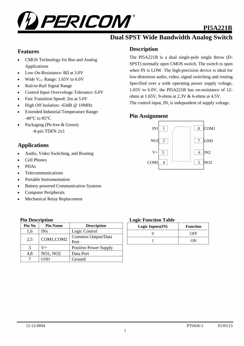
Pin Assignment
Pin Description Pin No Pin Name Description
1,6 INx Logic Control
2,5 COM1,COM2 Common Output/Data
Port
3 V+ Positive Power Supply
4,8 NO1, NO2 Data Port
7 GND Ground
Logic Function Table
Logic Inputs(IN) Function
0 OFF
1 ON
IN1 1
NO1 2
V+ 3
8 COM1
6 IN2
7 GND
COM2 4 5 NO2
|||||||||||||||||||||||||||||||||||||||||||||||||||||||||||||||||||||||||||||||||||||||||||||||||||||||||||||||||||||||||||||||||||||||||||||||||||||||||||||||||||||||||||||||||||||||||||||||||||||||||||||||||||||||||||||||||||||||||||||||||||||||||||||||||||||||||||||||||||||||||||||||||||||||||||||||||||||||||||||||||||||||||||||||||||||||||||||||||||||||||||||||||||||||||||||||||||||||||||||||||||||||||||||||||||||||||||||||||||||||||||||||||||||||||||||||||||||||||||
12-12-0004 PT0436-1 01/05/13
2
PI5A221B
Dual SPST Wide Bandwidth Analog Switch
PRELIMINARY INFORMATION: COMPANY CONFIDENTIAL
Maximum Ratings
Storage Temperature…………………………………...-65℃ to +150℃
Ambient Temperature with Power Applied......................-40℃ to +85℃
Supply Voltage V+ ………………………………………-0.3V to +7.0V
DC Control Voltage VIN
… …………………………….-0.5V to 7.0V
DC Input Voltage (VNO, VCOM)..................................-0.3V to V+ + 0.5V
DC Output Current IOUT… ……………………………………….128mA
DC V+ or Ground Current I+ /IGND … …………………………..±100mA
Junction Temperature under Bias (TJ) ...........................................150°C
Junction Lead Temperature (TL)
(Soldering, 10 seconds) ................................................................ 260°C
Power Dissipation (PD) @ +85°C ...............................................180mW
ESD (HBM)…………………………………………………..….2000V
Recommended Operating Conditions
Symbol Parameter Conditions Min. Typ. Max. Unit
V+ Operating Voltage - 1.65 - 6.0 V
VIN Control Input Voltage - 0 - 6.0 V
VINPUT Switch Input Voltage - 0 - V+ V
VOUT Output Voltage - 0 - V+ V
TA Operating Temperature - -40 25 85 °C
tr, tf Control Input Rise and
Fall Time
V+ = 2.3V to 3.6V 0 - 10 ns/V
V+ = 4.5V to 6.0V 0 - 5 ns/V
Note: Control input must be held HIGH or LOW; it must not float.
Note:
Stresses greater than those listed under MAXIMUM
RATINGS may cause permanent damage to the
device. This is a stress rating only and functional
operation of the device at these or any other
conditions above those indicated in the operational
sections of this specification is not implied.
Exposure to absolute maximum rating conditions
for extended periods may affect reliability.
|||||||||||||||||||||||||||||||||||||||||||||||||||||||||||||||||||||||||||||||||||||||||||||||||||||||||||||||||||||||||||||||||||||||||||||||||||||||||||||||||||||||||||||||||||||||||||||||||||||||||||||||||||||||||||||||||||||||||||||||||||||||||||||||||||||||||||||||||||||||||||||||||||||||||||||||||||||||||||||||||||||||||||||||||||||||||||||||||||||||||||||||||||||||||||||||||||||||||||||||||||||||||||||||||||||||||||||||||||||||||||||||||||||||||||||||||||||||||||
12-12-0004 PT0436-1 01/05/13
3
PI5A221B
Dual SPST Wide Bandwidth Analog Switch
PRELIMINARY INFORMATION: COMPANY CONFIDENTIAL
DC Electrical Characteristics
(TA = –40°C to 85°C, unless otherwise noted.)
Parameter Description Test Conditions Temperature Min Typ Max Units
VIAR Analog Input Signal Range V+ -40°C to 85°C 0 - 6 V
RON ON Resistance
(1)
V+=4.5V, IO = 30mA, VINPUT = 0V
25°C
- 4 6
V+=4.5V, IO=-30mA, VINPUT =2.4V - 5 8
V+=4.5V, IO =-30mA, VINPUT
=4.5V - 7 11
V+=4.5V, IO =30mA, VINPUT = 0V
-40°C to 85°C
- - 6
V+=4.5V, IO =-30mA,VINPUT =2.4V - - 8
V+=4.5V, IO =-30mA, VINPUT
=4.5V - - 11
V+=3.0V, IO =24mA, VINPUT =0V
25°C
- 5 8
V+=3.0V, IO =-24mA, VINPUT
=3.0V - 10 15
V+=3.0V, IO =24mA, VINPUT =0V -40°C to 85°C
- - 8
V+=3.0V, IO=-24mA, VINPUT =3.0V - - 15
V+=2.3V, IO =8mA, VINPUT =0V 25°C
- 6 9
V+=2.3V, IO =-8mA, VINPUT =2.3V - 13 20
V+=2.3V, IO =8mA, VINPUT =0V -40°C to 85°C
- - 9
V+=2.3V, IO=-8mA, VINPUT =2.3V - - 20
V+=1.65V, IO =4mA, VINPUT =0V
25°C
- 8 12
V+=1.65V, IO=-4mA,
VINPUT=1.65V - 20 30
V+=1.65V, IO =4mA, VINPUT= 0V
-40°C to 85°C
- - 12
V+=1.65V, IO=-4mA,
VINPUT=1.65V - - 30
RONF
ON Resistance
Flatness(1,2,3)
V+=5.0V, IA =-30mA,0≤VINPUT≤V+
25°C
- 6 -
V+=3.3V, IA =-24mA,
0≤VINPUT V+ - 12 -
V+=2.5V, IA =-8mA, 0≤VINPUT≤V+ - 22 -
V+=1.8V, IA =-4mA, 0≤VINPUT≤V+ - 90 -
VIH
Input High Voltage
(Logic High Level)
V+=1.65V
-40°C to 85°C
1 - -
V
V+ = 2.3V 1.2 - -
V+ = 3V 1.3 - -
V+ = 4.2V 1.5 - -
V+ = 6.0V 1.8 - -
VIL
Input Low Voltage
(Logic Low Level)
V+=1.65V
-40°C to 85°C
- - 0.4
V
V+ = 2.3V - - 0.6
V+ = 3V - - 0.8
V+ = 4.2V - - 1
V+ = 6.0V - - 1.2
ILKC Input Leakage Current 0≤VIN≤6.0V, V+=0V to 6.0V
25°C - - ±0.1 µA
-40°C to 85°C - - ±1.0
IOFF
OFF State Leakage
Current 0≤VIN≤6.0V, V+=1.65V to 6.0V
25°C - - ±0.1 µA
-40°Cto 85°C - - ±10
I+ Quiescent Supply Current All channels ON or OFF, VIN = V+ or GND, IOUT=0, V+ = 6.0V
25°C - - 1 µA
-40°C to 85°C - - 5
Notes:
1. Measured by voltage drop between COM and NO pins at the indicated current through the device. ON resistance is determined by the
lower of the voltages on two ports (COM or NO).
2. Parameter is characterized but not tested in production. 3. Flatness is defined as difference between maximum and minimum value of ON resistance over the specified range of conditions. Guaranteed
by design.
|||||||||||||||||||||||||||||||||||||||||||||||||||||||||||||||||||||||||||||||||||||||||||||||||||||||||||||||||||||||||||||||||||||||||||||||||||||||||||||||||||||||||||||||||||||||||||||||||||||||||||||||||||||||||||||||||||||||||||||||||||||||||||||||||||||||||||||||||||||||||||||||||||||||||||||||||||||||||||||||||||||||||||||||||||||||||||||||||||||||||||||||||||||||||||||||||||||||||||||||||||||||||||||||||||||||||||||||||||||||||||||||||||||||||||||||||||||||||||
12-12-0004 PT0436-1 01/05/13
4
PI5A221B
Dual SPST Wide Bandwidth Analog Switch
PRELIMINARY INFORMATION: COMPANY CONFIDENTIAL
Capacitance (1)
(TA = 25°C, unless otherwise noted.) Symbol Parameter Test Conditions Min. Typ. Max. Units
CIN Control Input
V+ = 5.0V, f =1 MHz(1)
- 2.5 -
pF COFF NO Port, Switch OFF - 5.0 -
CCOM ON COM Port, Switch ON - 15.0 -
Notes: 1. Capacitance is characterized but not tested in production
Switch and AC Characteristics (1)
Parameter Description Test Conditions Supply Voltage Temperature Min Typ Max Units
tON Turn-On Time RL=100Ω, CL=35pF
(2),
See Test Circuit Figure 1.
V+ =3.3V, VNO=3.0V,
VIH=3.0V, -40~+85°C
- 3.6 6
ns V+ =5.0V, VNO=3V,
VIL=3V, - 3 5
tOFF Turn-Off Time RL=100Ω, CL=35pF,
See Test Circuit Figure 1.
V+ =3.3V, VNO=3.0V,
VIH=3.0V, -40~+85°C
- 3 5
ns V+ =5.0V, VNO=3V,
VIL=3V, - 2.5 4
Q Charge Injection
CL = 1nF, V
GEN = 0V,
RGEN
=0.
See Test Circuit Figure 2.
V+ = 5.0V
25°C
- 5 -
pC V+ = 3.3V - 4 -
f3dB –3dB Bandwidth See Test Circuit Figure 5. V+ =1.65V to 5.5V 25°C - 500 - MHz
OIRR Off Isolation
RL=50, V
GEN=0V, R
GEN
=0, f =10MHz.
See Test Circuit Figure 6
V+ =1.65V to 5.5V 25°C - -63 - dB
Notes:
1. Guaranteed by design.
2. The device contributes no other propagation delay other than the RC delay of the switch ON resistance and the 35pF load capacitance,
when driven by an ideal voltage source with zero output impedance.

|||||||||||||||||||||||||||||||||||||||||||||||||||||||||||||||||||||||||||||||||||||||||||||||||||||||||||||||||||||||||||||||||||||||||||||||||||||||||||||||||||||||||||||||||||||||||||||||||||||||||||||||||||||||||||||||||||||||||||||||||||||||||||||||||||||||||||||||||||||||||||||||||||||||||||||||||||||||||||||||||||||||||||||||||||||||||||||||||||||||||||||||||||||||||||||||||||||||||||||||||||||||||||||||||||||||||||||||||||||||||||||||||||||||||||||||||||||||||||
12-12-0004 PT0436-1 01/05/13
5
PI5A221B
Dual SPST Wide Bandwidth Analog Switch
PRELIMINARY INFORMATION: COMPANY CONFIDENTIAL
Test Circuits and Timing Diagrams
Figure 1. Switching Time
Figure 2. Charge Injection
Figure 3. Channel-Off Capacitance
NO
NO
35pF

|||||||||||||||||||||||||||||||||||||||||||||||||||||||||||||||||||||||||||||||||||||||||||||||||||||||||||||||||||||||||||||||||||||||||||||||||||||||||||||||||||||||||||||||||||||||||||||||||||||||||||||||||||||||||||||||||||||||||||||||||||||||||||||||||||||||||||||||||||||||||||||||||||||||||||||||||||||||||||||||||||||||||||||||||||||||||||||||||||||||||||||||||||||||||||||||||||||||||||||||||||||||||||||||||||||||||||||||||||||||||||||||||||||||||||||||||||||||||||
12-12-0004 PT0436-1 01/05/13
6
PI5A221B
Dual SPST Wide Bandwidth Analog Switch
PRELIMINARY INFORMATION: COMPANY CONFIDENTIAL
Figure 4. Channel-On Capacitance
Figure 5. Bandwidth
NO

|||||||||||||||||||||||||||||||||||||||||||||||||||||||||||||||||||||||||||||||||||||||||||||||||||||||||||||||||||||||||||||||||||||||||||||||||||||||||||||||||||||||||||||||||||||||||||||||||||||||||||||||||||||||||||||||||||||||||||||||||||||||||||||||||||||||||||||||||||||||||||||||||||||||||||||||||||||||||||||||||||||||||||||||||||||||||||||||||||||||||||||||||||||||||||||||||||||||||||||||||||||||||||||||||||||||||||||||||||||||||||||||||||||||||||||||||||||||||||
12-12-0004 PT0436-1 01/05/13
7
PI5A221B
Dual SPST Wide Bandwidth Analog Switch
PRELIMINARY INFORMATION: COMPANY CONFIDENTIAL
Figure 6. Off Isolation
NO
COM
|||||||||||||||||||||||||||||||||||||||||||||||||||||||||||||||||||||||||||||||||||||||||||||||||||||||||||||||||||||||||||||||||||||||||||||||||||||||||||||||||||||||||||||||||||||||||||||||||||||||||||||||||||||||||||||||||||||||||||||||||||||||||||||||||||||||||||||||||||||||||||||||||||||||||||||||||||||||||||||||||||||||||||||||||||||||||||||||||||||||||||||||||||||||||||||||||||||||||||||||||||||||||||||||||||||||||||||||||||||||||||||||||||||||||||||||||||||||||||
12-12-0004 PT0436-1 01/05/13
8
PI5A221B
Dual SPST Wide Bandwidth Analog Switch
PRELIMINARY INFORMATION: COMPANY CONFIDENTIAL
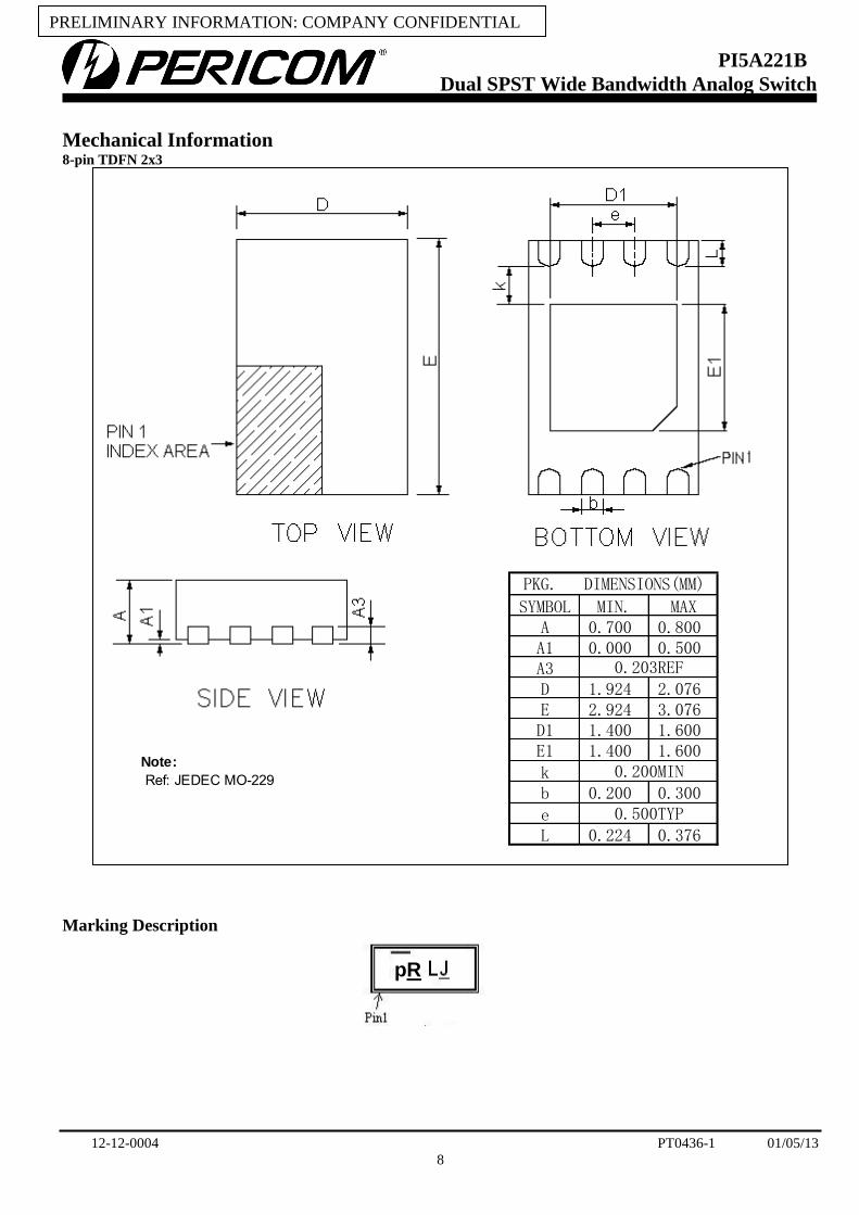
Mechanical Information 8-pin TDFN 2x3
Marking Description
SYMBOL MIN. MAXA 0.700 0.800A1 0.000 0.500A3D 1.924 2.076E 2.924 3.076D1 1.400 1.600E1 1.400 1.600kb 0.200 0.300eL 0.224 0.376
PKG. DIMENSIONS(MM)
0.203REF
0.200MIN
0.500TYP
Note:
Ref: JEDEC MO-229
pR
|||||||||||||||||||||||||||||||||||||||||||||||||||||||||||||||||||||||||||||||||||||||||||||||||||||||||||||||||||||||||||||||||||||||||||||||||||||||||||||||||||||||||||||||||||||||||||||||||||||||||||||||||||||||||||||||||||||||||||||||||||||||||||||||||||||||||||||||||||||||||||||||||||||||||||||||||||||||||||||||||||||||||||||||||||||||||||||||||||||||||||||||||||||||||||||||||||||||||||||||||||||||||||||||||||||||||||||||||||||||||||||||||||||||||||||||||||||||||||
12-12-0004 PT0436-1 01/05/13
9
PI5A221B
Dual SPST Wide Bandwidth Analog Switch
PRELIMINARY INFORMATION: COMPANY CONFIDENTIAL
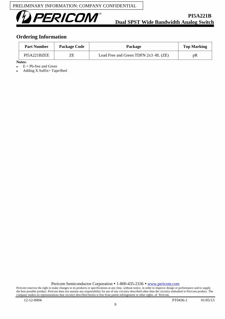
Ordering Information
Part Number Package Code Package Top Marking
PI5A221BZEE ZE Lead Free and Green TDFN 2x3 -8L (ZE) pR
Notes:
E = Pb-free and Green
Adding X Suffix= Tape/Reel
Pericom Semiconductor Corporation 1-800-435-2336 www.pericom.com Pericom reserves the right to make changes to its products or specifications at any time, without notice, in order to improve design or performance and to supply the best possible product. Pericom does not assume any responsibility for use of any circuitry described other than the circuitry embodied in Pericom product. The
company makes no representations that circuitry described herein is free from patent infringement or other rights, of Pericom.