physical electronics(ece3540) the pn junction...
TRANSCRIPT
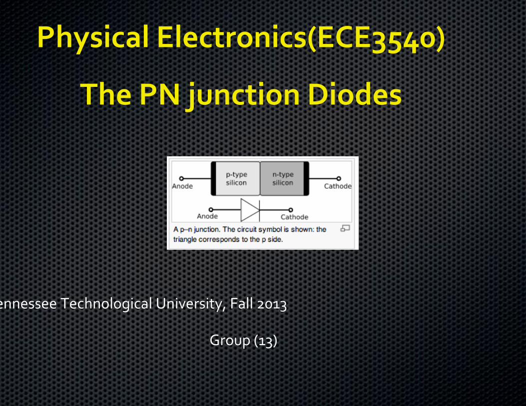
Physical Electronics(ECE3540)
The PN junction Diodes
ennessee Technological University, Fall 2013
Group (13)
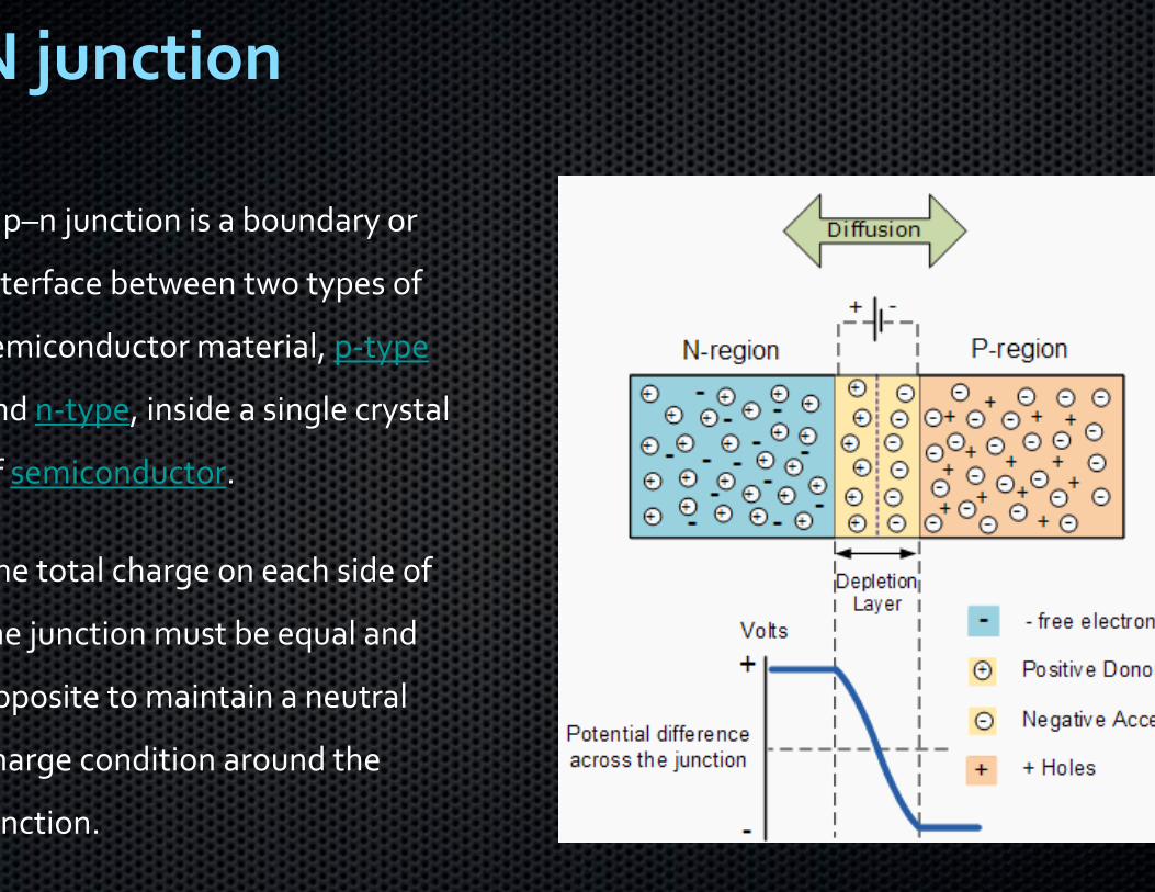
N junction
p–n junction is a boundary or
terface between two types of
emiconductor material, p‐type
nd n‐type, inside a single crystal
f semiconductor.
he total charge on each side of
he junction must be equal and
pposite to maintain a neutral
harge condition around the
nction.

N junction Diode
p–n junction diode is made of a crystal
f semiconductor. Impurities are added
o it to create a region on one side that
ontains negative charge carriers
lectrons), called n‐type semiconductor,
nd a region on the other side that
ontains positive charge carriers (holes),
alled p‐type semiconductor.
Typical diode packages in same alignmendiode symbol. Thin bar depicts the cathod
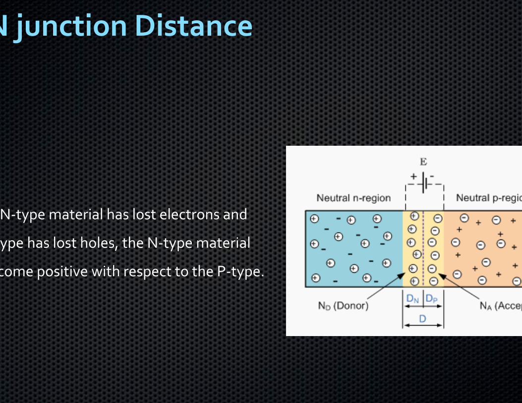
N junction Distance
N‐type material has lost electrons and
ype has lost holes, the N‐type material
come positive with respect to the P‐type.

N junction Distance
s electric field created by the diffusion process has created a "built‐in potential
erence" across the junction with an open‐circuit (zero bias) potential of:
ere:
s the zero bias junction voltage
s the intrinsic concentration.
the thermal voltage of 26mV at room temperature
and NA are the impurity concentrations

ow Current Diodes
hese diodes body is about 3mm long can
arry maximum forward current of about
00mA and withstand a reverse voltage of
5V without breaking down.

edium current Diodes
hese diodes can pass a forward current of
bout 500 mA and can withstand a reverse
oltage of 250 V.
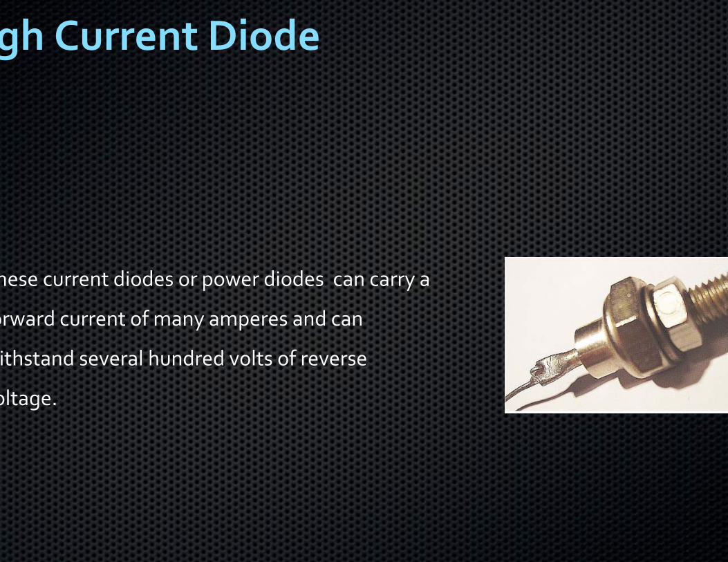
gh Current Diode
hese current diodes or power diodes can carry a
orward current of many amperes and can
ithstand several hundred volts of reverse
oltage.

ener Diode
is basically the same as the
tandard PN junction diode but
re specially designed to have a
w pre-determined Reverse
reakdown Voltage that takes
dvantage of this high reverse
oltage. The zener diode is the
mplest types of voltage regulator
nd the point at which a zener
ode breaks down or conducts is
alled the "Zener Voltage" ( Vz ). Electronic symbol
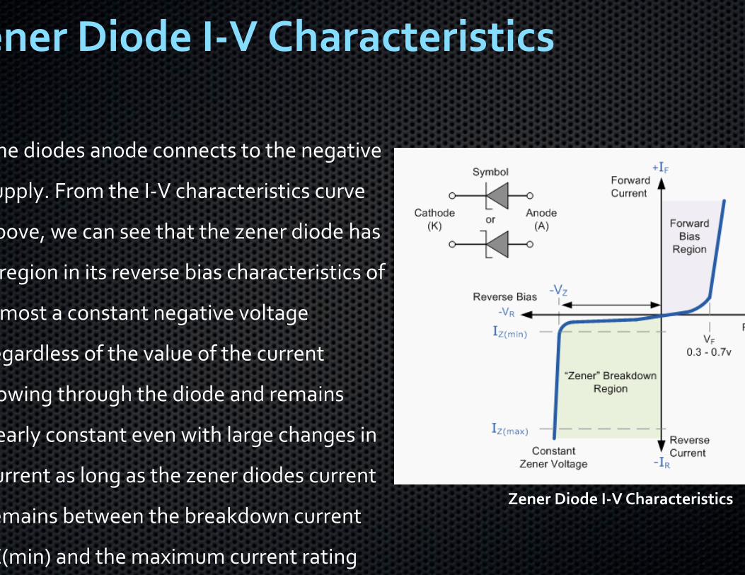
ener Diode I‐V Characteristics
he diodes anode connects to the negative
upply. From the I‐V characteristics curve
bove, we can see that the zener diode has
region in its reverse bias characteristics of
most a constant negative voltage
egardless of the value of the current
owing through the diode and remains
early constant even with large changes in
urrent as long as the zener diodes current
emains between the breakdown current
Z(min) and the maximum current rating
Zener Diode I‐V Characteristics

ercise
5.0V stabilised power supply is required to be produced from a
2V DC power supply input source. The maximum power rating
f the zener diode is 2W. Using the zener regulator circuit above
alculate:

olution for ( a , b )
e maximum current flowing through the zener diode.
e minimum value of the series resistor, RS

olution for ( c, d )
e load current IL if a load resistor of 1kΩ is connected across the Z
.
he zener current IZ at full load.

unnel Diode
tunnel diode or Esaki diode is a type of
emiconductor that is capable of very fast
peration, well into the microwave
equency region, made possible by the use
f the quantum mechanical effect called
unneling.
p
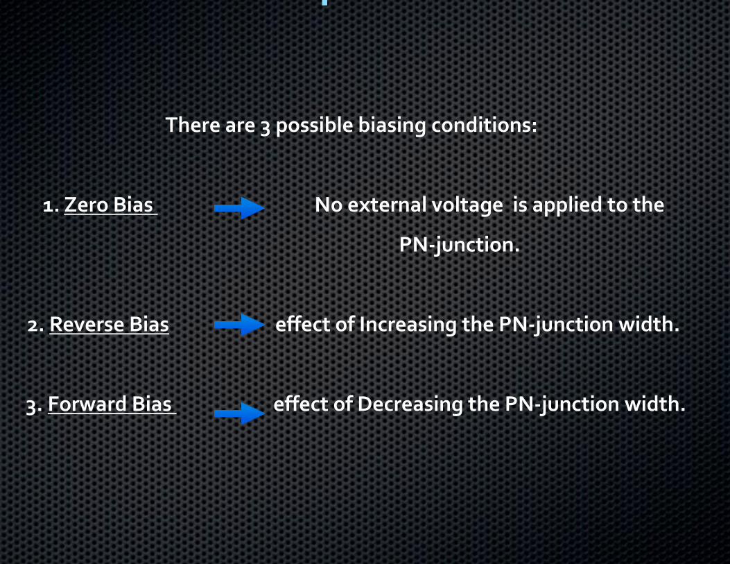
There are 3 possible biasing conditions:
1. Zero Bias No external voltage is applied to the
PN‐junction.
2. Reverse Bias effect of Increasing the PN‐junction width.
3. Forward Bias effect of Decreasing the PN‐junction width.
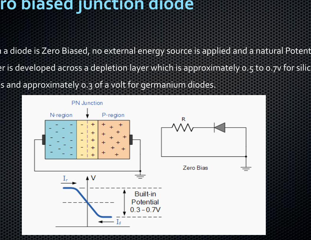
ro biased junction diode
n a diode is Zero Biased, no external energy source is applied and a natural Potent
er is developed across a depletion layer which is approximately 0.5 to 0.7v for silic
es and approximately 0.3 of a volt for germanium diodes.

hen a junction diode is Reverse Biased, the thickness of the depletion region
creases and the diode acts like an open circuit blocking any current flow, (only
very small leakage current).
Reverse resistance of a diode ranges from 5MΩ to 1000MΩ

junction diode is Forward Biased, the thickness of the depletion region reduces
de acts like a short circuit allowing full current to flow.

p
Forward Biased Diode Reverse Biased Diode
the junction temperature increases the de's characteristic shifts to the left.
oth, Silicon and Germanium this shift isabout 0.25mV/°C
an increase in the temperature causes ain saturation current (leakage)
Every increase of 10°C in junction temresults in approximate doubling of this
e generates heat and if the ambient temperature is high, this heat may not be diss
gh and will change the diode's parameters (characteristics).

• Reverse Bias the diode is reverse‐biased, a very small drift current due to thermal excitation fl the junction. This current (reverse saturation current,I0) is given, according to themann equation, by the formula
K0 is a constant depending on the pn junction geometry and V0 is the built‐in of the diode (see chapter “Semiconductor Materials: pn junction”)
Forward Bias
e diode is forward‐biased through a voltage V, a small drift current flows againe junction. In that case, however, there is an additional component, the diffusionVd, given by the formula:

eo link: e P‐N junction – How diodes work?
• http://www.youtube.com/watch?v=JBtEckh3L9Q

eference
orr, Wayne. "The PN Junction." PN Junction Theory for Semiconductor Diodes.
ayne Storr, 1999. Web. 31 Oct. 2013.
chey, Jason. "P–n Junction." Wikipedia. Wikimedia Foundation, 28 Oct. 2013.
eb. 31 Oct. 2013.