physical design challenges and solutions for emerging
TRANSCRIPT

Physical Design Challenges and Solutions for EmergingHeterogeneous 3D Integration Technologies
Lingjun [email protected]
Georgia Institute of TechnologyAtlanta, Georgia, USA
Sung Kyu [email protected]
Georgia Institute of TechnologyAtlanta, Georgia, USA
ABSTRACTThe emerging heterogeneous 3D integration technologies providea promising solution to improve the performance of electronicsystems in the post-Moore era, but the lack of design automationsolutions and the challenges in physical design are hindering theapplications of these technologies. In this paper, we discuss multipletypes and levels of heterogeneous integration enabled by the high-density 3D technologies. We investigate each physical implementa-tion stage from technology setup to placement and routing, identifythe design challenges proposed by heterogeneous 3D integration.This paper provides a comprehensive survey on the state-of-the-artphysical design methodologies to address these challenges.
CCS CONCEPTS•Hardware→ 3D integrated circuits; Physical design (EDA).
KEYWORDS3D ICs; physical design; heterogeneous integration
ACM Reference Format:Lingjun Zhu and Sung Kyu Lim. 2021. Physical Design Challenges andSolutions for Emerging Heterogeneous 3D Integration Technologies. InProceedings of the 2021 International Symposium on Physical Design (ISPD’21), March 22–24, 2021, Virtual Event, USA. ACM, New York, NY, USA,8 pages. https://doi.org/10.1145/3439706.3446903
1 INTRODUCTIONWith the growing demands of computing, storage, and signal con-version in modern electronic products, the performance improve-ment of the conventional 2D single-die integrated circuits (ICs),as predicted by Moore’s Law, are faced with increasing challenges.First of all, thermal and signal integrity issues can hinder the inte-gration of sufficient digital and analog units. In addition, the long2D interconnects tend to introduce significant wire delay and limitthe memory throughput. Moreover, it is difficult to select a singleprocess node to balance the performance, power, area (PPA) metricsfor a design. Therefore, it is time to look for other solutions beyondMoore’s Law.
Permission to make digital or hard copies of all or part of this work for personal orclassroom use is granted without fee provided that copies are not made or distributedfor profit or commercial advantage and that copies bear this notice and the full citationon the first page. Copyrights for components of this work owned by others than ACMmust be honored. Abstracting with credit is permitted. To copy otherwise, or republish,to post on servers or to redistribute to lists, requires prior specific permission and/or afee. Request permissions from [email protected] ’21, March 22–24, 2021, Virtual Event, USA© 2021 Association for Computing Machinery.ACM ISBN 978-1-4503-8300-4/21/03. . . $15.00https://doi.org/10.1145/3439706.3446903
The emerging 3D integration technologies enable us to tacklethese challenges from a third dimension. There are various typesof 3D integration technologies, including the Through-Silicon-Via-based 3D (TSV 3D), Face-to-Face-bonded 3D (F2F 3D), and mono-lithic 3D (M3D) ICs. Recent studies show that the minimum pitch ofthe TSVs and F2F micro bumps can be reduced to sub-10µm [5, 7],which allows high-density 3D integration of multiple dies. In ad-dition, the M3D ICs use the Monolithic inter-tier vias (MIVs) forvertical interconnects, which provide a even higher 3D interconnectdensity (up to 100 million/mm2) [25]. With these high-density 3Dintegration technologies, the designers can integrate a large num-ber of functional units in a 3D IC, achieve wire length and delayreduction, and improve the PPA design metrics. More importantly,3D technologies enable multiple types and levels of heterogeneousintegration.
Heterogeneous 3D integration is a promising solution to over-come the performance and cost limitations in conventional IC de-sign. Computer architects and circuit designers have studied differ-ent types and levels of heterogeneous 3D integration: (1) multipleheterogeneous processors can be integrated into a 3D IC to create aheterogeneous 3D chip multiprocessor (CMP); (2) various technol-ogy nodes can be utilized to fabricate different dies, and the dies arelater bonded together as a 3D IC with heterogeneous technology;(3) digital and analogy, or logic and memory components can beseparated to different dies to create a 3D IC with a heterogeneousfloorplan. In recent years, many studies have been done to investi-gate the potential benefits of one or more of these heterogeneous3D integration concepts. For example, Kim et al. implemented a 3Dprocessor named 3D-MAPS with 64 cores and 256kB stacked SRAMusing the TSV-based 3D and F2F 3D technology [11]; Srimani etal. integrated complementary carbon nanotube logic and resistiveRAM into a multi-tier monolithic 3D IC; Gomes et al. built a hybridprocessor system call Lakefield with 10nm and 22nm technologynodes [9]. However, the development of heterogeneous 3D ICs issignificantly affected by the challenges in physical design and thelack of electronic design automation (EDA) tools.
The existing EDA tools mostly target the conventional single-die2D IC with a specified technology node. In the design database, the2D tools usually store the X and Y coordinates of the standard cellsand optimize the placement based on these coordinates. Therefore,it is difficult to apply these tools to heterogeneous 3D ICs with oneadditional dimension. Also, the 2D routing engine cannot workin the routing space for heterogeneous 3D ICs directly, and it ischallenging to determine the 3D interconnect locations in high-density 3D ICs manually. Moreover, we need EDA tools to verifythe signal integrity and thermal reliability in heterogeneous 3D ICs.
Session 12: Physical Design at Advanced Technology Nodes ISPD '21, March 22–24, 2021, Virtual Event, USA
127

(a) (b)
(c)
Figure 1: Different 3D technologies can enable heteroge-neous 3D integration: (a) TSV-based 3D; (b) F2F-bonded 3D;(c) M3D [18].
This paper provides a comprehensive analysis of the physicaldesign challenges and solutions for the emerging 3D integrationtechnology. We look into the different types of heterogeneous 3DICs, and demonstrate the challenges in physical design. We presentan overview of the state-of-the-art solutions for each of the physi-cal design stages, including technology setup, partitioning, floor-planning, placement and routing, and verification. The article isorganized as follows: In section 1 and 2, we provide an introductionto different types and levels of heterogeneous 3D technology. Insection 3, we provide an in-depth analysis of the physical designchallenges in the heterogeneous 3D ICs. In section 4, we summarizethe state-of-the-art solutions to address the challenges and analyzetheir pros and cons. In section 5, we propose a few interesting topicsfor future studies. Section 6 concludes the paper.
2 OVERVIEW OF HETEROGENEOUS 3DINTEGRATION TECHNOLOGIES
In this section, we present an overview of multiple types and levelsof heterogeneous 3D ICs. We first introduce the heterogeneous 3DICs enabled by different 3D technologies. Then, we consider theheterogeneous integration at the computer architecture, technology,and floorplanning levels, respectively.
2.1 3D Technology EnablementFigure 1 shows that heterogeneous 3D integration can be enabled byall three technologies with various advantages and disadvantages.As shown in Figure 1a, TSVs are vertical vias that can penetrate thesilicon substrate of a die. Using TSVs, multiple dies with differentprocessors, technology nodes, or functions can be integrated into aTSV-based heterogeneous 3D IC. The typical size of TSVs rangesfrom 1µm to 10µm, and the pitch is usually 3-5µm. With a mature
small
core 1
small
core 2
small
core 3
small
core 4
big
core 1technology node A
technology node B
logic modules
memory blocks
(a) (b) (c)
Figure 2: A conceptual view of multiple levels of heteroge-neous 3D integration: (a) heterogeneous processors; (b) het-erogeneous technology nodes; (c) heterogeneous floorplan.
TSV fabrication process, the generated TSV-based 3D ICs usuallyhave high mechanical reliability thanks to the large size of the TSVs,compared with the other 3D technologies. However, TSVs requirea large keep-out zone (KOZ), which can occupy a large silicon areaand introduce an extra cost. In addition, the pitch of TSVs is stillrather large, which may limit the PPA benefits from heterogeneous3D integration. Also, the RC parasitics of each TSV is also negligible,which create additional RC delays in 3D ICs.
F2F 3D connects the back-end-of-line layers of two dies togetherin a face-to-face fashion using𝐶𝑢-𝐶𝑢 direct bonding [13], as shownin Figure 1b. This technology provides a higher interconnect density(with 1-2µm pitches), which can benefit the power delivery andsignal transmission between dies. Also, the F2F bonding pads donot occupy any silicon area since it is established on the top of theBEOL layers. The two dies can be fabricated and tested separately,which leads to a low manufacturing cost. However, the bondingfashion limits the number of dies to be integrated into two, and itintroduces some electrical and thermal coupling issues. Since theBEOL layers of both die are bonded together, the crosstalk betweenthe two die and the temperature increase due to the inferior heatdissipation rate are negligible in F2F 3D-based heterogeneous ICs.For heterogeneous integration, F2F 3D allows dies with differentprocessors and technology nodes to be bonded together. Both the3D-MAPS [11] and Lakefield [9] utilize the F2F bonding pads forinter-die signal transmission.
As shown in Figure 1, M3D ICs have the smallest 3D interconnectpitch, which is typically lower than 100nm, which is close to thepitch of the conventional nano-scale inter-layer vias (ILVs) in 2DICs. Therefore, this technology enables high integration densitywith more than 1 million per mm in heterogeneous 3D ICs. The highdensity allows us to optimize the 3D routing with 3D interconnectsexhaustively, while it proposes challenges for 2D routing tools sincethe cell pins are on different layers. In addition, the small MIVs havesmall RC parasitics. However, the manufacturing process requires alow-temperature process and may lead to performance degradation.
Session 12: Physical Design at Advanced Technology Nodes ISPD '21, March 22–24, 2021, Virtual Event, USA
128

2.2 Different Levels of Heterogeneous 3DIntegration
Figure 2 shows different levels of heterogeneous 3D integration.3D technologies facilitate the integration of heterogeneous multi-core processors, which can provide significant energy efficiencyimprovement for a multi-core computing system. For example, theLakefield 3D processor integrates one Sunny Cove big core, fourTremont small cores, and multiple multiple GPUs and IPU in thesystem [9]. The one big core can provide better single-thread per-formance and energy efficiency for heavy single-thread workloads.For more realistic workloads, the four small cores can provide abetter multi-thread performance and power efficiency. By choos-ing the processor core based on the workloads, the system canachieve significant performance improvement and energy savings.Although heterogeneous processors can be implemented in 2D ICs,such as Arm’s big.LITTLE architecture [2], the die area and manu-facturing cost limit the number of processor cores to be integratedin a single-die 2D IC. As the 2D die area increases with the increas-ing core number, the die yield decreases dramatically and leads togrowing manufacturing cost, based on the Murphy model [23] anda constant defect density (D0). On the other hand, 3D integrationof heterogeneous processors allows the designer to integrate morecores in a given 2D footprint area, and the short 3D interconnectscan help improve the inter-core communication throughput. Theheterogeneous processors do not introduce additional problems forphysical implementation (P&R) because the heterogeneity is onthe architectural level, but it requires signal integrity and thermalanalysis methods to verify the heterogeneous 3D ICs in order tomake sure the resulting multi-core processor can work sustainablyunder realistic workloads.
3D integration also allows the designers to incorporate multi-ple technology nodes for different components in a design. It isdifficult to select a technology node for a general-purpose com-pute platform and optimize the PPA metrics, since the trade-offbetween performance, power, and cost exists. The advanced high-performance technology nodes usually mean higher power con-sumption (especially for leakage power) and manufacturing cost,while the low-power technology has a lower cost but inferior perfor-mance. Therefore, a single technology node can hardly be optimalacross all the design metrics. However, heterogeneous 3D integra-tion allows us to integrate multiple dies from different technologynodes, as shown in Figure 2b. Using this technology, designerscan optimize the PPA metrics based on technology heterogeneity.For example, the Intel Foveros technology allows the designers tointegrate a high-performance 10nm technology node with an ultra-low-power 22nm technology node [10]. Based on this technology,The authors in [9] place the CPU and GPU cores on a compute diewith the 10nm technology, and place the interfaces and other ana-log components in a base die with the 22nm technology. By doingthis, they reduce the standby power of the system to 1/10th of theoriginal design with improved graphic performance and reducedarea. Heterogeneous technology nodes are a promising solution toimprove the performance and energy efficiency for next-generationcompute platforms, but it also requires significant modificationon technology setup, placement, and routing, since the existing
EDA tools cannot handle the heterogeneous 3D technology nodesdirectly.
Heterogeneous floorplanning is another level of heterogeneous3D integration. Modern system-on-chips (SoCs) often contains mul-tiple logic andmemory blocks, as well as digital and analog modules.In 2D ICs, these components need to be incorporated in a singlesilicon die, which leads to numerous signal integrity, power deliv-ery, placement, and routing optimization challenges. The idea ofheterogeneous floorplanning is to separate these components intodifferent dies in 3D, which can not only help address these chal-lenges, but also introduce additional performance and reliabilitybenefits. For instance, previous studies have proven the perfor-mance improvement achieved by the logic-on-memory heteroge-neous floorplanning [12, 20, 22]. However, the heterogeneous floor-plan proposes unique challenges for placement and routing sincethe components on each die are significantly different. As a result,the existing physical design methodologies for homogeneous 3DICs should not be directly applied to 3D ICs with a heterogeneousfloorplan; otherwise, it can lead to unexpected performance degra-dation. The details of the P&R challenges and the state-of-the-artsolutions will be discussed in the following sections.
3 PHYSICAL DESIGN CHALLENGES INHETEROGENEOUS 3D
3.1 Technology Setup ChallengesHeterogeneous 3D integration usually requires significant modifi-cation during the technology setup stage, especially with multipletechnology nodes, because conventional 2D EDA tools cannot han-dle heterogeneous 3D technology directly. For example, Cadence®InnovusTM provides a complete solution for 2D IC implementation.It uses the design exchange file (DEF) and library exchange file(LEF) to represent the physical design of a 2D IC. The LEF files de-fine the dimensions and topology of BEOL layers and standard celllibraries, and the DEF files store the placement and routing infor-mation. However, the LEF file does not allow us to define multipledevice layers, which means it cannot reflect the front-end-of-line(FEOL) structure of a heterogeneous 3D IC with two or more diesstraightforwardly. Innovus provides another method to setup thetechnology environment for micro-bump-based 3D ICs. It enablesusers to define micro-bump cells to represent the 3D interconnects,implement each die as if it is a 2D IC, and then bond the two dietogether in a top-level design. This flow can help users workaroundthe challenge to setup the 3D technology, while it only works forthe micro-bump-based design with a relatively low 3D interconnectdensity.
In addition, designing a complete 3D PDK to reflect the hetero-geneous 3D technology setup requires a large amount of work. Theauthors in [6] propose a 3D PDK generator based on the Open3DTM
LETI platform. The designers need to define a complete Design RuleManual including the 3D interconnection modules such as TSVs,micro-bumps, etc. However, the dimensions of the BEOL layers and3D interconnection structure are usually confidential to foundries,and the resulting 3D PDK may not be compatible with the P&R andverification tools in the following physical design stages.
Session 12: Physical Design at Advanced Technology Nodes ISPD '21, March 22–24, 2021, Virtual Event, USA
129

Shrunk-2D [16] and Compact-2D [14] are two physical designflows targeting gate-level 3D ICs (both heterogeneous and homo-geneous), and they setup the technology files based on existing 2DPDKs and P&R tools. Shrunk-2D shrinks the standard cell size andBEOL dimensions in a 2D technology node by a ratio of 0.707. Bydoing these, the P&R in a 2D design with the shrunk technologyfiles can represent the P&R in a homogeneous 3D design with thesame footprint area, because the area occupied by standard cellsand metal resources used for routing are equivalent. One issue withthis approach is that the parasitic resistance and capacitance (RC)extracted from the shrunk design is inaccurate and does not reflectthe real parasitics in 3D design, since the RLCs do not scale lin-early with wire dimensions. Compact-2D, on the other hand, doesnot need to shrink the cells or BEOL layers. Instead, it places androutes with the original standard cells, but scales the unit RC perwire length by 0.707. By doing this, it avoids the dimension errorsintroduced by cell and wire scaling and provides a better estimationof the RC delay. However, both Shrunk-2D and Compact-2D arefaced with challenges in 3D ICs with heterogeneous technologynodes. Because the 2D P&R tools cannot incorporate multiple tech-nology nodes in a single-die design, the Shrunk-2D or Compact-2Ddesign needs to be implemented in one technology node and thenbe separated into multiple dies with various technology nodes. Asa result, the placement and routing resource estimation during theinitial 2D stage is not very accurate for 3D ICs with heterogeneoustechnology nodes. More modifications need to be done to setup the3D technology for heterogeneous integration.
3.2 Tier Partitioning and FloorplanningChallenges
Tier partitioning is an important step for heterogeneous 3D IC im-plementation since it determines the technology nodes for differentcomponents, and has a huge impact on the following physical de-sign stages. However, the existing partitioning approaches mainlyfocus on the homogeneous setting with only standard cells, whichdoes not consider the impact of heterogeneous process nodes orfloorplan.
For example, recursive partitioning is a common method usedfor 3D tier partitioning [19]. The method consists of a series ofV-cuts (cut along the y-axis) and H-cuts (cut along the x-axis), anda Z-cut (separate the cells to different tiers). The sequence of V-cutsand H-cuts divides a 2D design into smaller sub-regions, and thelocation of the Z-cut in the sequence determines the number of3D interconnects. This method allows users to control the numberof 3D nets, but it does not consider the heterogeneous technologynodes on different dies.
A bin-based min-cut partitioning method is employed by Shrunk-2D and Compact-2D flows to implement gate-level 3D ICs with anarea balance constraint [17]. First, the initial 2D design is dividedinto rectangular bins with a specific number of columns and rows.We can adjust the bin size to control the outcome of the partitioningsolution, because cells in each bin will be partitioned into separatedtiers. Then, the Fiduccia–Mattheyses (FM) [8] algorithm is appliedwithin each bin, as shown in Fig. 3. As a result, the number of3D interconnects in each bin is minimized and the area balanceconstraint is satisfied. This approach can result in high design
Figure 3: The concept of the bin-based tier-partitioningmethod [17]. The left figure shows a projected 2D placementon half the area. The right figure shows the min-cut parti-tioning is being done within each rectangular bin.
quality for homogeneous 3D designs, because these designs mainlyconsist of standard cells of a single process node, so each tier isnearly identical and area balance is the only constraint. However,for 3D ICs with heterogeneous technology nodes, this approachcannot distinguish the differences between multiple process nodesand the resulting partition is not optimized. Therefore, a morecomprehensive tier partitioning approach is needed to incorporatethe architecture, technology, and functional differences betweentwo tiers in a heterogeneous 3D IC.
Generating a heterogeneous floorplan is also a challenging task,because multiple design metrics need to be considered during thisstage. For example, in a logic-on-memory heterogeneous 3D IC,the floorplan of the memory blocks on the memory die is criticalsince it can also affect the standard cell placement on the logic dieduring physical implementation. However, the existing EDA toolscannot generate heterogeneous 3D floorplan automatically, andmanual modification is required to optimize the floorplan for betterperformance and power consumption.
3.3 Placement and Routing ChallengesHeterogeneous 3D integration also proposes unique challenges forplacement and routing tools. With a heterogeneous floorplan, thelogic and memory modules of a design may be separated into differ-ent tiers, but ideally, the placement and routing of these modulesneed to be optimized simultaneously. However, conventional phys-ical design flows do not support this optimization in 3D ICs. Forinstance, the Shrunk-2D flow uses placement blockage to representthe memory blocks during the Shrunk-2D stage, as shown in Fig-ure 4. Based on the preplaced memory locations, the flow adds fullplacement blockages (𝑡 ′
𝑑= 0) in the regions where memory blocks
on top and bottom dies overlap; it also adds partial blockage withhalf of the placement density (𝑡 ′
𝑑= 𝑡𝑑 ) to guide the cell placement
in the region where there are memory blocks on only one die. Thismethod works well for design with only a few memory instances.However, for the heterogeneous 3D IC with a memory-on-logicfloorplan, it results in low placement quality. In the memory-on-logic design, one of the dies is fully occupied by memory blocks,which is converted to a large region of partial blockages in theShrunk-2D stage. But the partial blockage is not a hard constraint
Session 12: Physical Design at Advanced Technology Nodes ISPD '21, March 22–24, 2021, Virtual Event, USA
130

Figure 4:Memorymacro handling in the original Shrunk-2Dflow. (a) Initial memory placement. (b) Projection of mem-ory locations on a 2D plane. (c) Add placement blockage torepresent the memory blocks. [17].
during placement. The density of the placement solution is non-uniform and in some regions the local placement density is higherthan the limit (𝑡𝑑 ). This non-uniformity causes cell overlappingafter tier partitioning, and thus leads to a low placement quality.A similar problem exists in the Compact-2D flow since it also uti-lizes partial blockages to replace the memory and guide the cellplacement.
Shrunk-2D employs a die-by-die routing approach to implementsand optimizes 3D ICs. That is, after tier partitioning, the locationsof 3D inter-die interconnects are determined first. Then, the twodies of 3D ICs and routed separately based on the Shrunk-2D place-ment solution and the 3D interconnect locations. The impact of theother die is represented by external constraints (I/O delays, load ca-pacitance, etc.) extracted iteratively. However, with heterogeneousfloorplan or technology nodes, the differences between two dies canbe significantly large. As a result, the external constraints cannotreflect the real timing and signal coupling effects between the twodies. Moreover, the locations of the 3D interconnects are prefixedand cannot be updated during die-by-die routing, which may alsolead to an under-optimized routing solution. To mitigate these is-sues, the Compact-2D flow provides a post-partition optimizationfeature to optimize the routing results after the initial die-by-dierouting with a 3D metal stack. However, for heterogeneous 3DICs, this optimization needs to be done at an early design stageto achieve better P&R results. Experimental results in [1] showthat the memory-on-logic heterogeneous 3D ICs implemented with
Shrunk-2D can have worse performance compared to the original2D design, due to these placement and routing challenges.
3.4 Verification ChallengesSignal integrity, power delivery, and thermal analysis are neces-sary steps to verify the reliability of 3D ICs. Due to the higherpower density and smaller footprint area, 3D ICs tend to sufferfrom larger IR-drop [3] due and higher temperature [21]. However,the commercial EDA tools for signal integrity and thermal analysisfocus on 2D ICs, and usually require a complete 2D design databasewith technology files. In Shrunk-2D and Compact-2D flows, theparasitics of each die can be extracted separately for timing andsignal integrity analysis at the top level, but the inter-die electri-cal coupling is omitted during this procedure. Power delivery andthermal analysis also require a complete 3D view to analyze thecorrelation between multiple dies. Therefore, it is challenging toverify the signal integrity, power integrity, and thermal issues for aheterogeneous 3D ICs as a whole.
4 PHYSICAL DESIGN SOLUTIONS FORHETEROGENEOUS 3D
4.1 Heterogeneous 3D Technology SetupTo represent the heterogeneous 3D technology, one solution isto create a pseudo-3D metal stack based on the 2D technologynodes. Bamberg et al. in [1] propose a method to setup a 3D metalstack for memory-on-logic F2F heterogeneous 3D ICs. As shownin Figure 5, the BEOL layers of two dies are stacked together tocreate a 3D BEOL stack. In this 3D BEOL stack, the upper fourmetal layers are from the memory die, and the lower six metallayers are from the logic die, while the F2F via layer in between isused to represent the F2F bonding pads. The pins of the memoryblock on the memory die are also projected to the upper four metallayer of this BEOL stack, in order to reflect their exact locations inthe real 3D IC. The parasitics of the metal stack are characterizedbased on the dimensions of the layers using a commercial extractionengine. Furthermore, the memory blocks on the memory die areshrunk into the minimal size and pre-placed on a 2D plane beforestandard cell placement. Using this technology setup, the existing2D EDA tools can complete the placement and routing based onthe real 3D routing space with accurate wirelength estimation andparasitic extraction results. Experimental results in [1] show thatthis configuration has nearly no performance or energy penaltycompared with the setting with six metal layers on each die, whileit helps reduce the manufacturing cost.
Notice that this method can be applied to represent heteroge-neous technology nodes by characterizing the 3D BEOL stack basedon the metal layer dimensions from multiple technology nodes.Also, the components on the memory die are not limited to mem-ory, but include analog blocks or other physical IPs as well, whichenables analog-on-digital heterogeneous 3D integration.
A similar approach is proposed in [24] but targeting monolithic3D ICs. Unlike the F2F 3Dmethod, theM3D BEOL stack is bonded ina face-to-back manner and logic-on-memory integration providesa better solution for MIV placement compared to memory-on-logic,due to the large size of the memory blocks. To prevent the MIV fromoverlapping with standard cells, an obstruction with the same size
Session 12: Physical Design at Advanced Technology Nodes ISPD '21, March 22–24, 2021, Virtual Event, USA
131
bump
layer
F2F via
layer
macro
pins
Figure 5: Technology setup formemory-on-logic F2F hetero-geneous 3D ICs [1].
as the standard cell is added to the MIV layer for each correspond-ing standard cell. This setup enables the 2D commercial tools tooptimize the P&R for heterogeneous M3D ICs as well, which resultsin high utilization of MIVs (more than 400,000) for a RISC-V micro-processor and 23% area reduction at iso-performance compared toa 2D baseline.
4.2 Heterogeneous 3D Partitioning andFloorplanning
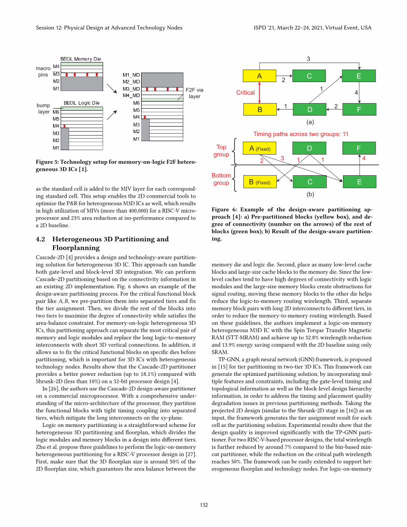
Cascade-2D [4] provides a design and technology-aware partition-ing solution for heterogeneous 3D IC. This approach can handleboth gate-level and block-level 3D integration. We can performCascade-2D partitioning based on the connectivity information inan existing 2D implementation. Fig. 6 shows an example of thedesign-aware partitioning process. For the critical functional blockpair like 𝐴, 𝐵, we pre-partition them into separated tiers and fixthe tier assignment. Then, we divide the rest of the blocks intotwo tiers to maximize the degree of connectivity while satisfies thearea-balance constraint. For memory-on-logic heterogeneous 3DICs, this partitioning approach can separate the most critical pair ofmemory and logic modules and replace the long logic-to-memoryinterconnects with short 3D vertical connections. In addition, itallows us to fix the critical functional blocks on specific dies beforepartitioning, which is important for 3D ICs with heterogeneoustechnology nodes. Results show that the Cascade-2D partitionerprovides a better power reduction (up to 18.1%) compared withShrunk-2D (less than 10%) on a 32-bit processor design [4].
In [26], the authors use the Cascade-2D design-aware partitioneron a commercial microprocessor. With a comprehensive under-standing of the micro-architecture of the processor, they partitionthe functional blocks with tight timing coupling into separatedtiers, which mitigate the long interconnects on the xy-plane.
Logic on memory partitioning is a straightforward scheme forheterogeneous 3D partitioning and floorplan, which divides thelogic modules and memory blocks in a design into different tiers.Zhu et al. propose three guidelines to perform the logic-on-memoryheterogeneous partitioning for a RISC-V processor design in [27].First, make sure that the 3D floorplan size is around 50% of the2D floorplan size, which guarantees the area balance between the
A (Fixed) D F
B (Fixed) C E
4
(b)
A C E
B D F
2
3
14
21
(a)
Critical
1132
Top
group
Bottom
group
Timing paths across two groups: 11
Figure 6: Example of the design-aware partitioning ap-proach [4]: a) Pre-partitioned blocks (yellow box), and de-gree of connectivity (number on the arrows) of the rest ofblocks (green box); b) Result of the design-aware partition-ing.
memory die and logic die. Second, place as many low-level cacheblocks and large-size cache blocks to the memory die. Since the low-level caches tend to have high degrees of connectivity with logicmodules and the large-size memory blocks create obstructions forsignal routing, moving these memory blocks to the other die helpsreduce the logic-to-memory routing wirelength. Third, separatememory block pairs with long 2D interconnects to different tiers, inorder to reduce the memory-to-memory routing wirelength. Basedon these guidelines, the authors implement a logic-on-memoryheterogeneous M3D IC with the Spin Torque Transfer MagneticRAM (STT-MRAM) and achieve up to 32.8% wirelength reductionand 13.9% energy saving compared with the 2D baseline using onlySRAM.
TP-GNN, a graph neural network (GNN) framework, is proposedin [15] for tier partitioning in two-tier 3D ICs. This framework cangenerate the optimized partitioning solution, by incorporating mul-tiple features and constraints, including the gate-level timing andtopological information as well as the block-level design hierarchyinformation, in order to address the timing and placement qualitydegradation issues in previous partitioning methods. Taking theprojected 2D design (similar to the Shrunk-2D stage in [16]) as aninput, the framework generates the tier assignment result for eachcell as the partitioning solution. Experimental results show that thedesign quality is improved significantly with the TP-GNN parti-tioner. For two RISC-V-based processor designs, the total wirelengthis further reduced by around 7% compared to the bin-based min-cut partitioner, while the reduction on the critical path wirelengthreaches 50%. The framework can be easily extended to support het-erogeneous floorplan and technology nodes. For logic-on-memory
Session 12: Physical Design at Advanced Technology Nodes ISPD '21, March 22–24, 2021, Virtual Event, USA
132

3D ICs, we can add an additional constraint to limit the standardcell placement to the logic die. For 3D ICs with multiple technologynodes, we can introduce timing and power scaling factors to modifythe features and reflect the impact of different technology nodes.
4.3 Heterogeneous 3D Placement and RoutingCascade-2D [4] is an effective P&R methodology to implementheterogeneous 3D ICs. It also utilizes 2D P&R tools, but representthe 3D interconnects with a unique structure based on anchor cellsand dummy wires. Figure 7 shows an example of the Cascade-2D3D interconnect. The two dies are placed side-by-side on a 2Dplane, while a pair of anchor cells and dummy wire establish theconnection from the bottom-most layer of the top die to the top-most layer of the bottom die. This structure can accurately modelthe real 3D interconnect because the dummy wires have zero RCparasitics and MIV parasitics are included in the final timing stage.After the partitioning stage described in section 4.2, the flow firstdetermines the locations of the MIVs by implementing the twodie sequentially. After that, the MIV ports and anchor cells areadded to each die. Then, the 3D design is assembled, placed, androuted as a whole. The Cascade-2D methodology overcomes a fewimportant disadvantages in the Shrunk-2D and Compact-2D flows:(1) No scaling factor is applied to the wire dimensions or parasitics,which avoids the errors introduced by scaling; (2) The anchor cellsand dummy wires model the 3D interconnect accurately, which isbetter than the routing resource estimation during the Shrunk-2Dor Compact-2D stages; (3) The flow does not need to use partialblockages to handle the memory blocks. This helps prevent thetiming degradation caused by cell overlapping and thus enables theimplementation of logic-on-memory heterogeneous 3D ICs.
On the basis of Cascade-2D, Xu et al. propose another method,multi-tier co-placement (MTCP), to improve the P&R quality of3D ICs [26]. In this flow, the 3D interconnect locations are notfixed during the implementation. Instead, it updates the locationsof the anchor cells together with other standard cell placementiteratively. By applying a hard fence bounding each anchor cell andvirtual anchor cell pair, it limits the placement space for anchorcells in the next iteration and ensures that the anchor cells willconverge to the optimized locations for the 3D interconnects. Withthis improvement, the flow is able to achieve even high frequency ina commercial processor design compared to Cascade-2D, togetherwith 41% power reduction compared to 2D at a near-iso-frequencypoint.
4.4 Heterogeneous 3D VerificationIn [28], the authors propose a tile-based thermal analysis flow anda holistic parasitic extraction method to verify the thermal andsignal integrity in heterogeneous 3D ICs. The tile-based thermalanalysis flow is an efficient and accurate method to simulate andgenerate the thermal profile of an entire 3D IC considering inter-diethermal coupling. In this flow, a 3D IC is first divided into squaretiles of the same size on the xy-plane, and then divided into cubesalong with each fabrication layer on the z-axis. Then, we createthe power map on the device active layer using the vector-basedpower analysis results. That is, we generate the time-based powerwaveform for specific workloads, select two clock cycles with the
Figure 7: Cascade-2D flow for monolithic 3D implementa-tion. (a) Cascade-2D implementation with anchor cell anddummy wires, which models (b) an equivalent M3D IC(adopted from [4]).
max power values, and then calculate the power consumption oneach tile based on the distribution. This tile-based power map re-flects the worst-case heat generation in the 3D IC and acts as aheat source during thermal analysis. After that, we analyze thethermal conductivity for each cube based on the material proper-ties of the device and BEOL layers. Within each cube, the verticalthermal resistors are in parallel because they consist of differentmaterials and the heat flow is distributed throughout the materials,while the lateral thermal resistors are in series. We create a thermalconductivity map by putting all the cubes together. With both thepower map and thermal conductivity map, we perform the thermalanalysis using the commercial thermal solver. This flow capturesthe thermal coupling between the two dies, because the thermalcubes from both dies are put together and the thermal equationsare solved as a whole. The thermal coupling is significant in F2Fheterogeneous 3D IC since the BEOL layers are bonded and theheat dissipation rate is low.
5 FUTURE STUDIESAlthough the recent studies have overcome many issues proposedby heterogeneous 3D integration, there are still numerous questionsthat remain unanswered, which may hinder the practical applica-tion of heterogeneous 3D ICs. First, the existing synthesis methodis not aware of any heterogeneous 3D configuration and cannotoptimize the design based on the technology configurations. Thecurrent physical-aware synthesis tools are able to incorporate 2Dphysical information during synthesis, but for 3D ICs with multi-ple different technology nodes, there is still potential to optimize
Session 12: Physical Design at Advanced Technology Nodes ISPD '21, March 22–24, 2021, Virtual Event, USA
133

the timing and power based on the architectural and technologyinformation at the synthesis stage.
True 3D PDK and placer are still required to implement morepractical heterogeneous 3D ICs. The pseudo-3D approaches (whichuses 2D EDA tools to implement 3D designs) cannot make full useof 3D placement and routing resources, and their applications arelimited. In the future, more studies should be done to facilitate3D PDK generation, enable true 3D placement and routing, andprovide signal integrity, power integrity, and thermal verificationfor heterogeneous 3D ICs.
6 CONCLUSIONSIn this paper, we look into different levels of heterogeneous 3D ICs,from the ICs with heterogeneous technology nodes, to the oneswith heterogeneous floorplans. We identify the challenges proposedby heterogeneous 3D integration at each physical design stage. Bycomparing the state-of-the-art physical design flows, we evaluatethe solutions to address these physical design challenges. We findthat the 3D BEOL stack is a good approach to describe the heteroge-neous 3D technology, which facilitates the placement and routingwith commercial 2D tools. Machine-learning-based partitioning andfloorplanning provide a promising solution for heterogeneous 3DICs with multiple technology nodes. On the other hand, more stud-ies on 3D-technology-aware synthesis and true 3D placement needto be done to further improve the performance of heterogeneous3D ICs and pave the way for more practical applications.
ACKNOWLEDGMENTSThis research is partially funded by the DARPA ERI 3DSOC Programunder Award HR001118C0096, the Semiconductor Research Corpo-ration under Task 2929, and the National Research Foundation ofKorea under NRF-2020M3F3A2A02082445.
REFERENCES[1] Lennart Bamberg et al. 2020. Macro-3D: A Physical Design Methodology for
Face-to-Face-Stacked Heterogeneous 3D ICs. In 2020 Design, Automation & Testin Europe Conference & Exhibition (DATE). IEEE.
[2] Anastasiia Butko, Florent Bruguier, Abdoulaye Gamatié, Gilles Sassatelli, DavidNovo, Lionel Torres, and Michel Robert. 2016. Full-system simulation of big. littlemulticore architecture for performance and energy exploration. In 2016 IEEE10th International Symposium on Embedded Multicore/Many-core Systems-on-Chip(MCSOC). IEEE, 201–208.
[3] Kyungwook Chang, Shidhartha Das, Saurabh Sinha, et al. 2017. Frequency andTime Domain Analysis of Power Delivery Network for Monolithic 3D ICs. In2017 IEEE/ACM International Symposium on Low Power Electronics and Design(ISLPED). IEEE, 1–6.
[4] Kyungwook Chang, Saurabh Sinha, Brian Cline, et al. 2016. Cascade2D: A Design-Aware Partitioning Approach to Monolithic 3D IC with 2D Commercial Tools. InProceedings of the 35th International Conference on Computer-Aided Design. ACM,130.
[5] YH Chen, CA Yang, CC Kuo, MF Chen, CH Tung, WC Chiou, and Douglas Yu.2020. Ultra High Density SoIC with Sub-micron Bond Pitch. In 2020 IEEE 70thElectronic Components and Technology Conference (ECTC). IEEE, 576–581.
[6] Gerald Cibrario, D Henry, C Chantre, R Cuchet, A Berthelot, Karim Azizi-Mourier,Marjorie Gary, and Fabien Gays. 2013. A 3D process design kit generator basedon customizable 3D layout design environment. In 2013 IEEE International 3DSystems Integration Conference (3DIC). IEEE, 1–5.
[7] Joeri De Vos, Stefaan Van Huylenbroeck, Anne Jourdain, Nancy Heylen, LanPeng, Geraldine Jamieson, Nina Tutunjyan, Stefano Sardo, Andy Miller, and EricBeyne. 2018. " Hole-in-One TSV", a New Via Last Concept for High Density3D-SOC Interconnects. In 2018 IEEE 68th Electronic Components and TechnologyConference (ECTC). IEEE, 1499–1504.
[8] Charles M Fiduccia and Robert M Mattheyses. 1982. A linear-time heuristicfor improving network partitions. In 19th design automation conference. IEEE,
175–181.[9] Wilfred Gomes, Sanjeev Khushu, Doug B Ingerly, Patrick N Stover, Nasirul I
Chowdhury, Frank O’Mahony, Ajay Balankutty, Noam Dolev, Martin G Dixon,Lei Jiang, et al. 2020. Lakefield and Mobility Compute: A 3D Stacked 10nm and22FFL Hybrid Processor System in 12× 12mm 2, 1mm Package-on-Package. In2020 IEEE International Solid-State Circuits Conference-(ISSCC). IEEE, 144–146.
[10] DB Ingerly, S Amin, L Aryasomayajula, A Balankutty, D Borst, A Chandra, KCheemalapati, CS Cook, R Criss, K Enamul, et al. 2019. Foveros: 3D Integra-tion and the use of Face-to-Face Chip Stacking for Logic Devices. In 2019 IEEEInternational Electron Devices Meeting (IEDM). IEEE, 19–6.
[11] D. H. Kim, K. Athikulwongse, M. Healy, M. Hossain, M. Jung, I. Khorosh, G.Kumar, Y. Lee, D. Lewis, T. Lin, C. Liu, S. Panth, M. Pathak, M. Ren, G. Shen, T.Song, D. H. Woo, X. Zhao, J. Kim, H. Choi, G. Loh, H. Lee, and S. K. Lim. 2012.3D-MAPS: 3D Massively parallel processor with stacked memory. In 2012 IEEEInternational Solid-State Circuits Conference. 188–190. https://doi.org/10.1109/ISSCC.2012.6176969
[12] Dae Hyun Kim, Krit Athikulwongse, Michael B Healy, et al. 2013. Design andAnalysis of 3D-MAPS (3D Massively Parallel Processor with Stacked Memory).IEEE Trans. Comput. 64, 1 (2013), 112–125.
[13] Sarah Eunkyung Kim and Sungdong Kim. 2015. Wafer level Cu–Cu direct bondingfor 3D integration. Microelectronic Engineering 137 (2015), 158–163.
[14] Bon Woong Ku, Kyungwook Chang, and Sung Kyu Lim. 2018. Compact-2D: APhysical Design Methodology to Build Commercial-Quality Face-to-Face-Bonded3D ICs. In Proceedings of the 2018 International Symposium on Physical Design.ACM, 90–97.
[15] Yi-Chen Lu, Sai Surya Kiran Pentapati, Lingjun Zhu, Kambiz Samadi, andSung Kyu Lim. 2020. TP-GNN: a graph neural network framework for tierpartitioning in monolithic 3D ICs. In 2020 57th ACM/IEEE Design AutomationConference (DAC). IEEE, 1–6.
[16] Shreepad Panth, Kambiz Samadi, Yang Du, et al. 2017. Shrunk-2-D: A PhysicalDesign Methodology to Build Commercial-quality Monolithic 3-D ICs. IEEETransactions on Computer-Aided Design of Integrated Circuits and Systems 36, 10(2017), 1716–1724.
[17] Shreepad Panth, Kambiz Samadi, Yang Du, and Sung Kyu Lim. 2015. Placement-driven partitioning for congestion mitigation in monolithic 3D IC designs. IEEETransactions on Computer-Aided Design of Integrated Circuits and Systems 34, 4(2015), 540–553.
[18] Shreepad A Panth, Kambiz Samadi, Yang Du, and Sung Kyu Lim. 2014. Design andCAD methodologies for low power gate-level monolithic 3D ICs. In Proceedingsof the 2014 international symposium on Low power electronics and design. 171–176.
[19] Mohit Pathak, Young-Joon Lee, Thomas Moon, and Sung Kyu Lim. 2010. Through-silicon-via management during 3D physical design: When to add and how many?.In 2010 IEEE/ACM International Conference on Computer-Aided Design (ICCAD).IEEE, 387–394.
[20] S. S. K. Pentapati, L. Zhu, L. Bamberg, et al. 2019. A Logic-on-Memory Processor-System Design with Monolithic 3D Technology. IEEE Micro (2019). https://doi.org/10.1109/MM.2019.2944330
[21] Sandeep Kumar Samal, Shreepad Panth, Kambiz Samadi, et al. 2014. Fast andAccurate Thermal Modeling and Optimization for Monolithic 3D ICs. In 201451st ACM/EDAC/IEEE Design Automation Conference (DAC). IEEE, 1–6.
[22] M. M. Shulaker, T. F. Wu, et al. 2014. Monolithic 3D Integration of Logic andMemory: Carbon Nanotube FETs, Resistive RAM, and Silicon FETs. In IEEEInternational Electron Devices Meeting.
[23] Charles H Stapper. 1991. On Murphy’s yield integral (IC manufacture). IEEEtransactions on semiconductor manufacturing 4, 4 (1991), 294–297.
[24] Sebastien Thuries, Olivier Billoint, Sylvain Choisnet, Romain Lemaire, PascalVivet, Perrine Batude, and Didier Lattard. 2020. M3D-ADTCO: monolithic 3Darchitecture, design and technology co-optimization for high energy efficient 3DIC. In 2020 Design, Automation & Test in Europe Conference & Exhibition (DATE).IEEE, 1740–1745.
[25] M Vinet, P Batude, C Fenouillet-Beranger, et al. 2014. Monolithic 3D Integration:A Powerful Alternative to Classical 2D Scaling. In 2014 SOI-3D-SubthresholdMicroelectronics Technology Unified Conference (S3S). IEEE, 1–3.
[26] Xiaoqing Xu, Mudit Bhargava, Steve Moore, Saurabh Sinha, and Brian Cline.2019. Enhanced 3D Implementation of an Arm® Cortex®-A Microprocessor. In2019 IEEE/ACM International Symposium on Low Power Electronics and Design(ISLPED). IEEE, 1–6.
[27] Lingjun Zhu, Lennart Bamberg, Anthony Agnesina, Francky Catthoor, DragomirMilojevic, Manu Komalan, Julien Ryckaert, Alberto Garcia-Ortiz, and Sung KyuLim. 2020. Heterogeneous 3D Integration for a RISC-V System With STT-MRAM.IEEE Computer Architecture Letters 19, 1 (2020), 51–54.
[28] Lingjun Zhu, Kyungwook Chang, Dusan Petranovic, Saurabh Sinha, Yun SeopYu, and Sung Kyu Lim. 2020. Full-Chip Electro-Thermal Coupling Extraction andAnalysis for Face-to-Face Bonded 3D ICs. In Proceedings of the 2020 InternationalSymposium on Physical Design. 39–46.
Session 12: Physical Design at Advanced Technology Nodes ISPD '21, March 22–24, 2021, Virtual Event, USA
134