physical and technological aspects of solar cells based on
TRANSCRIPT

Chapter 5
Physical and Technological Aspects of Solar Cells Basedon Metal Oxide-Silicon Contacts with Induced SurfaceInversion Layer
Oleksandr Malik and F. Javier De la Hidalga-W
Additional information is available at the end of the chapter
http://dx.doi.org/10.5772/53389
1. Introduction
With the current concerns about the worldwide environmental security, global warming,and climate change due to the emission of CO2 from the burning of fossil fuels, it is desirableto have a wide range of alternative energy technologies. Photovoltaic, or solar cells, have al‐ready proven themselves to be a viable option as a nonpolluting renewable energy source,as well as a visible business that will grow stronger in the global economy of present andfuture centuries.
The main problems of global practical application of solar cells for energy production aretheir low efficiency (typically of about 10-15%) and the cost of photovoltaic modules($200-500/m2). Monocrystalline silicon is the main material for the fabrication of solar cells. Itis the most studied material, and the lifetime of silicon solar cells and modules is 15-30years. The higher efficiency of silicon solar cells (up to 24%) that can be achieved using acomplicated cell design, and applying new technological processes, lead to an undesirableincrease of their total cost. From this point of view, solar cells based on more simple Schott‐ky contacts and metal-insulator-semiconductor (MIS) structures are promising for solar en‐ergy conversion due to their relatively low production cost.
Since 1978, a new class of photovoltaic devices, namely the semiconductor-insulator-semi‐conductor (SIS), has emerged, using a deposited conductive top layer made of a degeneratedwide-bandgap oxide semiconductor. Excellent results have been reported using tin-dopedindium oxide (In2O3:Sn or ITO). Other oxide semiconductors, such as fluorine-doped tin ox‐ide (SnO2:F) and doped zinc-oxide (ZnO), have also been used as a transparent conductingelectrode.
© 2013 Malik and De la Hidalga-W; licensee InTech. This is an open access article distributed under the termsof the Creative Commons Attribution License (http://creativecommons.org/licenses/by/3.0), which permitsunrestricted use, distribution, and reproduction in any medium, provided the original work is properly cited.

Thin films of these oxides behave as a metal, thus such SIS structures present electrical prop‐erties similar to those presented by MIS devices. Of course, the optical and photoelectricalproperties of SIS structures exceed the properties of MIS devices.
In our chapter of the book “Solar Energy”, edited by Radu D. Rugescu [1], the reader canfind a complete bibliography regarding the SIS solar cells and the properties of transparentconducting oxides fabricated using different methods.
In that book, a preceding discussion regarding the fabrication process of SIS solar cells, thestructural, electrical and optical properties of ITO and SnO2:F thin films, as well as the physi‐cal model of spray deposited ITO-Si solar cells and theirs properties has been presented. Itwas shown that such structures present a high barrier height that is not typical for Schottkydiodes. The authors developed a physical model of the ITO-Si solar cells based on an inver‐sion p-n junction similar to that reported by J. Shewchun et al. [2] for MIS structures with anAl electrode. According to this model, the I-V characteristics are dominated by a diffusioncurrent flow in the bulk of the silicon substrate and show the usual behavior for a Shockleydiode.
The aim of this chapter is to discuss some new physical aspects of spray deposited ITO-Sisolar cells which are tightly connected with the fabrication technology. Below, we will showthat suitable process schedules for chemical treatment of the silicon surface with the pres‐ence of acceptor-type surface states, is the reason for the inversion of the conductivity typeat the silicon surface. A sufficiently high potential barrier can be formed before the depositionof the ITO film if a minimum amount of fixed charge appears within the interfacial layervery close to the silicon surface. Then the role of the ITO electrode is the formation of anohmic contact on the inversion layer.
2. Barrier height of MIS solar cells
Solar cells based on contact metal-semiconductor with a Schottky barrier really representMIS structures due to the existence of a thin insulator layer between the metal and the semi‐conductor. MIS solar cells are receiving increasing attention because they present several in‐herent advantages such as low cost, high yield, fabrication at low substrate temperature, etc.However, one drawback of such cells is that their open-circuit voltage is slightly low anddepends on the potential barrier height.
The expression to calculate the barrier height ϕBn for n-type substrates is given by [3]
( ) ( )( )011 ox
Bn m s gs
QE
D qgf g f c g f
æ ö-= - + - - - ç ÷ç ÷
è ø(1)
where
Application of Solar Energy124

1
1 s
i
q Ddg
e
-æ ö
= +ç ÷ç ÷è ø
(2)
Here, ϕm is the metal work function, χs is the semiconductor electron affinity, Eg is the semi‐conductor energy gap, ϕ0 is energy level of surface states at the semiconductor surface, δ is
insulator (oxide) thickness, Ds is density of surface states, and Qoxq represents the amount of
fixed charge lying within the interfacial layer very close to the insulator-semiconductor in‐terface; the other symbols have their usual meaning. Figure 1 shows the calculated variationof the barrier height with the metal work function for different values of interfacial layerthickness [3]
3.8 4.0 4.2 4.4 4.6 4.8 5.0 5.2
0.0
0.2
0.4
0.6
0.8
1.0
3 nm
2 nm
d= 1 nm
1 nm
2 nm
d=3 nm
Substrate: silicon n-type
a- Without chargeb- With charge 2x10¹² charges/cm2
b
a
BA
RR
IER
HE
IGH
T, f
Bn (
eV)
METAL WORK FUNCTION, fm (eV)
Figure 1. Calculated variation of the barrier height with metal work function for different values of the interfacial lay‐er thickness [3].
These calculations were conducted assuming Ds=3x10¹² states/cm2/eV and ϕ0=0.27 eV for sili‐con. Positive oxide (insulator) charge was fixed to 2x10¹² charges/cm2. The positive sign ofthe charge is typical for several chemical methods used for the fabrication of thermal thinoxide on the silicon surface. It is clear that the existence of this charge decreases the barrierheight even if the metal work function is as high as 5.2 eV; for this case, the barrier heightdoes not exceed 0.8 eV.
Another situation becomes apparent when the fixed charge is negative, for example, in pres‐ence of acceptor-like surface states. In this case the sign of the third term in equation (1) ispositive, and a higher value of the barrier height is possible. Thermally grown oxide on thesilicon surface usually presents a positive fixed charge, however it may be possible to intro‐
Physical and Technological Aspects of Solar Cells Based on Metal Oxide-Silicon Contacts…http://dx.doi.org/10.5772/53389
125

duce a negative charge in the oxide by developing suitable process schedules for the chemi‐cal treatment of the semiconductor surface.
3. Relation between the charge and surface potential
For our discussion, we must find a relationship between the charge on the semiconductorsurface Qsand the surface potential ϕs. Considering a semiconductor having donor and ac‐ceptor impurities Nd and Na, respectively, completely ionized at room temperature, we needto solve the Poisson equation
d 2φd x 2 = −
4πρε ; ρ =q Nd −Na + p(x)−n(x) .
Using the boundary conditions:
φ =φs⊳0 at x =0,
φ →0, dφ / dx →0 at x →∞.
In the semiconductor volume we consider charge neutrality:
Nd + p =n + Na,
where p and n are the concentrations of electrons and holes, respectively, and
n(x)=nexp(qφ / kT ), p(x)= pexp(−qφ / kT ).
Defining n / ni =ni / p =γ and ψ =qφ / kT .
Then the Poisson equation can be written as
d 2ψd x 2 = −
4πq 2niεkT γ(1−expψ) + γ −1(exp(−ψ)−1
After integrating both sides with respect to ψ and determining the integration constant fromthe boundary conditions: ψ →0 and dψ / dx →0 at x →∞
( dψdx )2
= L D−2 γ(expψ −1) + γ −1(exp(−ψ)−1) + ψ(γ −1−γ)
Where L D−2 =8πq 2ni / εkT , and ni is the intrinsic carrier concentration.
It is easy to obtain a differential equation for the potential ϕ in the form
dϕdx = − (kT / qL D) γ(exp( qϕ
kT )−1) + γ −1(exp− ( qϕkT )−1) +
qϕkT (γ −1−γ)
1/2
At x=0, the boundary condition is εEx=0 =4πQs,
Where Ex=0 = −dϕ / dx, and Ex=0 is electric field at the surface of the semiconductor.
Finally, we obtain
Application of Solar Energy126

1/21 12 (exp 1) (exp 1) ( )s s s
s i Dq q q
Q qn LkT kT kTj j j
g g g g- -é ùæ ö æ ö= - + - - + -ê úç ÷ ç ÷
ê úè ø è øë û(3)
Here, φs⊳0, and Qs is a positive charge. For an n-type semiconductor, a band bending willbe developed due to the accumulation of electrons at the semiconductor surface.
For a negative charge Qs, we need to change the sign of φs in equation (3).
Figure 2 shows the calculated dependences of the negative Qs on the surface potential at thesilicon surface for different concentrations of donors in the silicon substrate.
0,4 0,6 0,8 1,0
10-9
10-8
10-7
10-6
1x10⁻⁵
1x10⁻⁴
10-3
s=0.75 V
Qs=-8x10
-8 C/cm
2
6
5
4
3
2
1
Qs(C
/cm
2)
s(V)
1 Nd=10
12 cm
-3
2 Nd=10
13 cm
-3
3 Nd=10
14 cm
-3
4 Nd=5x10
14 cm
-3
5 Nd=10
15 cm
-3
6 Nd=10
16 cm
-3
Figure 2. Calculated dependence of Qs on the surface potential at the silicon surface for different donor concentra‐tions in the silicon substrate.
We will discuss the properties of solar cells fabricated on n-type silicon with Nd=5×1014 cm-3.If a negative charge Qs=8x10⁻⁸ C/cm2 is present on the Si surface, the surface potential 0.75 eVis due to the strong inversion condition because qφs >2(EF −Ei)=0.28eV , where EF and Ei arethe Fermi and intrinsic energy levels in the silicon substrate, respectively.
4. Surface potential of the silicon wafers after a chemical cleaning
For any technical application, the silicon wafer must be subjected to a certain schedule ofchemical treatment. These are very important technological steps necessary to prevent thecontamination of the future device from non-controlled sources such as some metals thatcan introduce deep energy levels into the substrate.
The RCA Standard Cleaning, developed by W. Kern and D. Puotinen in 1965, and disclosedin 1970, is extremely effective for removing contamination from silicon surfaces, and it is a
Physical and Technological Aspects of Solar Cells Based on Metal Oxide-Silicon Contacts…http://dx.doi.org/10.5772/53389
127

current industry standard. The RCA cleaning has two sequential steps: the Standard Clean‐ing 1 (SC-1), followed by Standard Cleaning 2 (SC-2): The SC-1 solution, consisting of a mix‐ture of ammonium-hydroxide (NH4OH), hydrogen-peroxide (H2O2), and water (H2O), is themost efficient particle removing agent found to date. This mixture is also referred to as theAmmonium-Hydroxide/Hydrogen-Peroxide Mixture (APM).
In the SC-1 cleaning solution, the formation of native oxide (SiO2) by hydrogen peroxide andthe etching of the silicon oxide by alkalis (NH4OH) operate simultaneously. For this reason,the overall wafer thickness is slowly reduced, but certain thickness of SiO2 forms on the wa‐fer surface. In the past, the SC-1 solution presented a tendency to deposit metals on the sur‐face of the wafers, and consequently a treatment with the SC-2 mixture (H2O: HCl: H2O)were necessary to remove metals.
It is possible to consider SC-1 and SC-2 solutions as agents for wet chemical oxidation of thesilicon wafer due to the formation of a thin silicon dioxide layer during the treatment of thewafer in these solutions. Other chemical agents such as HCl, HNO3, the H2SO4:H2O2 mix‐ture, hydrogen-peroxide (H2O2), and water (H2O), can also be used for wet chemical oxida‐tion. With a suitable thickness and physical parameters, these oxide layers can be used forthe fabrication of MIS solar cells. However, the question is what the thickness of the siliconoxide layer will be obtained and which surface potential on the wafer will be developed af‐ter applying this technological procedure? One more question is connected with the densityof surface states after the wet chemical oxidation.
Many researchers have tried to find the answer to these questions. For instance, a completeinvestigation on this issue was conducted by Angermann [4]; some parameters of the oxidelayers formed with different chemical agents are shown in Table 1.
Oxidizing solutions Composition T [0C]Treatment time
(min)
Dit,min
[x1012 cm-2eV-1]<dox> [nm]
SC-1 6:1:1 75 10 6 1.1
SC-2 5:1:1 75 10 5 1.3
SC-1+SC-2 - 75 10+10 6 1.2
H2SO4:H2O2 1:1 120 5 5 1.8
HCl 36% 40 5 3 -
HNO3 65% 60 5 8 -
Deonized H2O 18 MΩ-cm 80 120 0.41.5 Si (111)
2.5 Si (100)
Table 1. Parameters of the oxide layer formed with different chemical agents [4], Dit,min is the minimum density ofsurface states.
Application of Solar Energy128

Other published results [5, 6] present a thickness of the oxide in the range of 0.8-1 nm aftertreatment in SC-1 solution. From Table1 it is clear that the best result regarding the mini‐mum density of surface states is obtained by using hot water. With other chemical agentsDit,min exceeds the value of 1012 cm-2eV-1. After etching in NH4F during 6.5 min, the oxidethickness obtained with the SC-1 solution decreases to 0.3 nm, and the density of surfacestates is 1x1011 cm-2eV-1. Such parameters are suitable for the fabrication of Schottky diodesbased on metal-semiconductor structures.
Now, it is interesting to know the band bending of the silicon surface after different process‐es for obtaining the chemical grown oxide. Again, and according to reference [4], the posi‐tion of the Fermi level EFs=EF-Ei (at x=0), determined at the n-type Si surface, with bulk Fermilevel Efb=EF-Ei (x>0) =-0.32 eV, after HF and NH4F and subsequent wet chemical oxidation invarious solutions, is shown in table 2.
Chemical etching Wet chemical oxidation agent
HF NH4F SC-1 SC-2 H2SO4/H2O2 HCl HNO3 H2O
+0.32 -0.02/+0.1 -0.25 +0.1 -0.03 +0.18 +0.2 ≅0
Table 2. Fermi level position EFs=EF-Ei (at x=0) determined on n-type Si surfaces when the bulk Fermi level is Efb=EF-Ei
(x>0) =-0.32 eV, after HF and NH4F, and subsequent wet chemical oxidation in various solutions.
The HF treatment leads to a strong inversion layer on H-terminated p-type silicon surfaces,which results from a positive charge induced by electronegative surface groups (-H, -O-H,and –F) on the surface silicon atoms. Using NH4F as the final etching agent under clean-room conditions, the remaining amount of surface charges results from the electro-negativi‐ty difference between silicon and hydrogen.
After the wet-chemical oxidation of initially H-terminated surfaces, characteristic values ofthe surface Fermi-level EFs, as shown in Table 2, were obtained from the interface-trappedcharge and from different kinds of oxide charges.
Most of the oxidizing solutions SC-2, HCl, and HNO3 cause a strong depletion of holes on p-type silicon surfaces due to the positive fixed oxide charge, which is also known from CVmeasurements of thermally grown oxides.
In contrast, the SC-1 process causes a negative surface charge, which is possible to originatefrom the dissociation of ≡Si-OH groups of the oxide layer in the alkaline solution (≡Si-OH ⇔≡Si-O-+H+).
From this reported results we make an important conclusion regarding the use of an n-typesilicon substrate: the forming of transparent for carriers insulating layer after wet oxidationand the formation of a depletion or inversion layer on the silicon surface after substratetreatment in the SC-1 solution. All other treatments in wet oxidizing solutions will producean accumulation band bending.
Physical and Technological Aspects of Solar Cells Based on Metal Oxide-Silicon Contacts…http://dx.doi.org/10.5772/53389
129

5. Chemical oxide after treatment in hydrogen-peroxide
The chemical oxide can also be created on the silicon surface with the treatment of the waferin an aqueous solution of hydrogen-peroxide. Neuwald et al. [7] shown that a very thin(about 0.5 nm) oxide is formed after immersion of a (111) silicon wafer in ultrapure 30%H2O2 solution. XPS analysis shows that the oxide thickness saturates on this level after 10minutes of immersion in the solution. Other results published by Verhaverbeke et al. [8] dis‐cuss in detail the limitation of the oxide thickness obtained in H2O2 and SC-1 solutions. Theyshow that the oxide thickness obtained in H2O2 solutions for different concentrations asfunction of time does not exceed 0.9 nm. In order to explain this experimental fact they usedthe results of Stoneham and Tasker, where the effect of image charges and their influence onthe grown oxide films are studied. These authors found that the polarization energies associ‐ated with localized charges near the interface between oxides and silicon provide a drivingforce, over short distances, which affect the transport of peroxide anions HO2
- (principal oxi‐dant) to the silicon surface. As the oxide thickness grows, the image charge reduces thetransport of the ionic species, and the oxidation process is limited. According to Verhaver‐beke, the model based on the charge transport (Figure 3) that predicts the frequently ob‐served limitation of an oxide thickness of around 0.8-1 nm, may also be applied to the oxidegrown in SC-1 solutions with a certain content of hydrogen-peroxide. It is not possible toknow in advance the sign of the charge in the oxide formed with ultrapure H2O2, but belowwe show that the presence of some impurities in the hydrogen-peroxide solution can changedrastically the situation.
HO2-
H2O2
HO2-
Solution Oxide Silicon
Image
force
Figure 3. Schematic illustration of Image Charge transport in H2O2 and SC-1 solutions [8].
6. Chemical oxide fabricated with a contaminated SC-1 solution
Generally, silicon wafers always present some charge in either, chemically or thermallygrown native oxide. It is well known that a fixed positive charge appears on thermally oxi‐dized Si wafers. It is also known that a large positive fixed oxide charge appears in naturally
Application of Solar Energy130

oxidized Si wafers soon after they are dipped in an aqueous hydrofluoric acid (HF), andthen the charge decreases as the native oxide grows in air. Munakata and Shimizu [9,10] re‐ported that when silicon wafers are rinsed by an SC-1 solution, a fairy large negative chargeof 5.8x011 charges/cm2 is observed in commercially available n-type Si wafers. In this case,the wafers were rinsed with the SC-1 solution in a Pyrex glass container. The charge was sig‐nificantly smaller when the treatment was conducted using a quartz container; this is be‐cause the Al (and also Fe) concentration in quartz is generally more than one order ofmagnitude lower than that found in Pyrex glass. This fact clearly suggests that some speciesin the SC-1 solution must be the cause of the negative charge, whose density should bemuch higher than that of the positive fixed oxide charge. At this moment, the exact chemicalmechanism of the negative charge formation is not clear. Authors assumed that the negativecharge arises from (AlSiO)- networks, when 3-valence Al substitutes 4-valence Si in the ox‐ide. The role of Al to form the negative oxide charge on the Si surface after rinsing with theSC-1 solution was verified with especially Al-contaminated SC-1 solutions. The same resultswere also obtained using 3-valence iron (Fe)–contaminated solutions.
It is known that Al atoms can isomerically substitute the Si atoms forming a wide class of(SiO2) x x (Al2O3) y, and Al can penetrate in the SiO2 film at a depth of about 100 nm. The Alatoms in the SiO2 film break partially or completely the dπ -πσ bounds. In three-coordinatedstates, these atoms are strong acceptors of electrons.
We assume that the negative charge can also appear in oxides obtained using Al (or Fe)-con‐taminated hydrogen-peroxide (H2O2) solutions.
7. Work function of tin-doped indium oxide (ITO) films
In this section we discuss the work function (qϕITO) of the ITO film. The data about the val‐ue of qϕITO is not presented systematically in the literature. This parameter presents a strongdependence on the fabrication method, structure and morphology of the film, and also onthe carrier concentration. Reported results for films obtained by thermal evaporation give awork function of 5.0 eV [11]. The work function of pure In2O3 films obtained by RF magnet‐ron sputtering was found to be in the range of 5.3-5.4 eV [12], and in contrast, the work func‐tion of ITO films with 5-20 wt. % Sn was found in the 4.6-4.8 eV range.
The work function of the ITO films fabricated by pyrosol technique was reported around 4.8eV, without an additional thermal treatment, whereas it was around 5.2 eV after a thermaltreatment [13].
In the case of n-type degenerated semiconductors, such as the ITO films, the work functionis expected to shift when the carrier concentration ne changes. It is inversely proportional tone
2/3; nevertheless, an opposite trend has been found for the relationship between the opticalenergy gap E g
opt and ne. The Fermi energy in the film conduction band should vary for anincreasing or decreasing ne. Therefore, the control of the work function with ne in the ITOlayers is an important issue to take into account for the estimation of the energy barriers in
Physical and Technological Aspects of Solar Cells Based on Metal Oxide-Silicon Contacts…http://dx.doi.org/10.5772/53389
131

Schottky and MIS devices. According to Sato et al. [14], the optical band gaps of the ITOfilms deposited by dc magnetron sputtering increased from 3.8 to 4.3 eV when the carrierdensity increased from 8.8x10¹⁹ to 8.2x1020 cm-3, whereas the work function decreased from5.5 to 4.8 eV. The variation of the optical band gap (Eg
opt) and the work function (ϕ), as afunction of the two-thirds power of the carrier density (ne
2/3) for undoped In2O3 and ITOfilms, is shown in Figure 4.
Figure 4. Variation of the optical band gap (Eg opt) (solid circles) and the work function (ϕ) (open circles) as a function
of the two-thirds power of the carrier density (ne2/3) for undoped In2O3 and ITO films [14].
For our solar cell we are using Sn-doped indium oxide films (ITO) fabricated by spray pyrol‐ysis technique. The optimized films have a carrier concentration of about 1021 cm-3, and theshift of the Fermi level is about 0.5 eV. Taking into account the reported data about the workfunction, we will use qϕITO= 4.8 eV.
8. Fabrication of ITO and FTO films by spray pyrolysis
The spray pyrolysis technique was employed for the deposition of thin ITO and FTO filmson glass and sapphire substrates in order to investigate their structural, electric, and opticalproperties. A 10 Ω-cm n-type (100)-silicon substrate, chemically cleaned and specially treat‐ed, was used for the fabrication of solar cells. The apparatus (atomizer) for the spray deposi‐tion was designed for obtaining small-size droplets. The substrates were mounted on aheater covered with a carbon disc for obtaining uniform temperature. Spraying was madeusing compressed air. Periodical cycles of the deposition with duration of 1 sec and intervalsof 5 sec were employed to prevent a rapid substrate cooling. The deposition rate was high,of about 200 nm/min. For the ITO films deposition, 13.5 mg of InCl3 were dissolved in a 170ml mixture of ethylic alcohol and water in a 1:1 proportion, and adding 5ml of HCl. The dif‐ferent ratios of Sn/In achieved in the ITO films were controlled by adding in the solution acalculated amount of tin chloride (SnCl4*5H2O). The substrate temperature, in the range of
Application of Solar Energy132

380-4800C, was controlled using a thermocouple with an accuracy of ±50C. The optimum dis‐tance from the atomizer to the substrate and the compressed air pressure were 25 cm and 1.4kg/cm2, respectively. Figure 5 shows schematically the equipment set-up.
Figure 5. Set-up of the equipment used for the deposition of the ITO films. Insert (a) shows the modification of theequipment for the purpose of mass-production.
9. Characterization equipment and methods
The film thickness was measured with an Alpha Step 200 electronic profilometer. The elec‐trical resistivity, Hall mobility and carrier concentration were measured at room tempera‐ture using the van der Pauw method. Hall effect parameters were recorded for a magneticfield of 0.25 Tesla. The optical transmission spectrum was obtained using a spectrophotome‐ter. The structural characterization was carried out with an X-ray diffractometer operating inthe Bragg-Brentano Θ-Θ geometry with Cu Kα radiation. A JSPM 5200 atomic force micro‐scope was used to study the film surfaces. The chemical composition of the films was deter‐mined using an UHV system of VG Microtech ESCA2000 Multilab, with an Al- Kα X-raysource (1486.6 eV) and a CLAM4 MCD analyzer.
10. Properties of the spray deposited ITO films
The X-ray diffraction (XRD) measurements shown in Figure 6 indicate that all deposited ITOfilms, with thicknesses in the 160-200 nm range, and fabricated from the chemical solutionsfor different Sn/In ratios, presents a cubic bixebyte structure in a polycrystalline configura‐tion with (400) as the preferential grain orientation
Physical and Technological Aspects of Solar Cells Based on Metal Oxide-Silicon Contacts…http://dx.doi.org/10.5772/53389
133

10 20 30 40 50 60 700
2000
4000
6000
8000
(622)(611)(440)(411)
(400)
(222)
T=480 °C [Sn]/[In]=0 % [Sn]/[In]=5 % [Sn]/[In]=11 %
Cou
nts
(a. u
.)
2 (grad)
Figure 6. XRD spectra of the ITO films fabricated using precursors with different Sn/In ratios. The mean size of thegrains, 30-50 nm, was determined using the classical Debye-Scherrer formula from the half-wave of the (400) reflec‐tions of the XRD patterns.
A surface roughness of about 30 nm was determined from images of the film surfaces ob‐tained with an atomic force microscope (Figure 7).
Figure 7. Atomic force images of the In2O3 film (left) and the ITO film with 5% Sn/In (right).
Figures 8 and 9 show the dependence of the electric parameters of deposited ITO film on the ra‐tio Sn/In used in the solution for the fabrication of the films. The sheet resistance Rs shown inFigure 8 has a minimum 12 Ω/□ for the films prepared using a solution with 5% Sn/In ratio.
The minimum resistivity obtained for the films deposited with a 5% Sn/In solution is 2×10 -4
Ω-cm. The variation of carrier concentration as a function of the Sn/In ratio in the precursorsis shown in Figure 9. The carrier concentration presented a value of 1.1x1021 cm-3 at the 5%Sn/In ratio. This high value is comparable with better results achieved when other techno‐logical methods are used for the fabrication of the ITO thin films.
Application of Solar Energy134

0 2 4 6 8 10 12
20406080
100
3000
3500T=480 °C
[Sn]/[In] ratio in the solution [%]
Rs (
) R
s
50
100
150
200
250
300
Thic
knes
s (n
m)
thickness
Figure 8. The sheet resistance as a function of the Sn/In ratio in the precursor used for the film deposition. The thick‐nesses of the films are also shown.
Figure 9. Variation of the carrier concentration as a function of the Sn/In ratio.
The optical transmission of indium oxide films for two thicknesses deposited on glass sub‐
strates, as a function of the wavelength, is shown in Figure 10.
Physical and Technological Aspects of Solar Cells Based on Metal Oxide-Silicon Contacts…http://dx.doi.org/10.5772/53389
135

Figure 10. Optical transmission of the ITO films for two thicknesses as a function of the wavelength
The use of sapphire substrates allows for determining the optical energy gap of the ITOfilms by the extrapolation of the linear part of the α2(hν) curves to α2=0, where α is the ab‐sorption coefficient. The optical gap increases with the carrier concentration due to the wellknown Moss-Burstein shift. For ITO films fabricated using the solution with a 5% Sn/In ra‐tio, this shift is 0.5 eV, and the optical gap is 4.2 ± 0.1 eV. Such high value of the optical gapoffers transparency in the ultraviolet range, which is of fundamental importance in solar cellapplications. Because of the opposite dependence of conductivity (σ) and transmission (T) ofthe ITO film on its thickness (t), both parameters must be optimized. A performance com‐parison of different films is possible using ϕTC =T 10 / Rs =σtexp(−10at) as a figure of merit[21]. Table 3 compares the values of ϕTC for spray deposited ITO films reported in this workwith some results obtained by other authors but using a different deposition technique.
Process Rs, Ω/□ T (%) ϕTC, (Ω-1) ×10-3 Reference
spray 26.0 90 13.4 [15]
spray 9.34 85 21 [16]
spray 10.0 90 34.9 [17]
spray 4.4 85 44.7 [18]
sputtering 12.5 95 47.9 [19]
evaporation 25.0 98 32.6 [20]
spray 12.0 93.7 43.5 [1] and this work
Table 3. Comparison of the values of ϕTC for the ITO films
Application of Solar Energy136
11. Solar cells fabrication
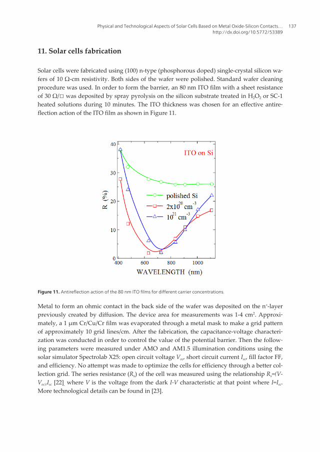
Solar cells were fabricated using (100) n-type (phosphorous doped) single-crystal silicon wa‐fers of 10 Ω-cm resistivity. Both sides of the wafer were polished. Standard wafer cleaningprocedure was used. In order to form the barrier, an 80 nm ITO film with a sheet resistanceof 30 Ω/□ was deposited by spray pyrolysis on the silicon substrate treated in H2O2 or SC-1heated solutions during 10 minutes. The ITO thickness was chosen for an effective antire‐flection action of the ITO film as shown in Figure 11.
Figure 11. Antireflection action of the 80 nm ITO films for different carrier concentrations.
Metal to form an ohmic contact in the back side of the wafer was deposited on the n+-layerpreviously created by diffusion. The device area for measurements was 1-4 cm2. Approxi‐mately, a 1 μm Cr/Cu/Cr film was evaporated through a metal mask to make a grid patternof approximately 10 grid lines/cm. After the fabrication, the capacitance-voltage characteri‐zation was conducted in order to control the value of the potential barrier. Then the follow‐ing parameters were measured under AMO and AM1.5 illumination conditions using thesolar simulator Spectrolab X25: open circuit voltage Voc, short circuit current Isc, fill factor FF,and efficiency. No attempt was made to optimize the cells for efficiency through a better col‐lection grid. The series resistance (Rs) of the cell was measured using the relationship Rs=(V-Voc)/Isc [22], where V is the voltage from the dark I-V characteristic at that point where I=Isc.More technological details can be found in [23].
Physical and Technological Aspects of Solar Cells Based on Metal Oxide-Silicon Contacts…http://dx.doi.org/10.5772/53389
137

12. Properties of the solar cells
The potential barrier height of the ITO/n-Si solar cells determined from the capacitance-volt‐age (C-V) characteristics is 0.9 eV. This high value of the potential barrier let us considersuch structures as pseudo classical diffusion p-n junctions. Thus, it is possible to expect thatthe diffusion of holes in the silicon bulk is the main carrier transport mechanism instead ofthe thermo-ionic emission in the Schottky and the metal/tunnel oxide/semiconductor struc‐tures. Moreover, C-V measurements of the potential barrier in structures with a created in‐version layer deliver an incorrect the potential barrier [24]. The barrier determined with thismethod is lower than the actual value.
A straightforward measurement of the temperature dependence of the dark current is, inprinciple, sufficient to identify a bipolar device in which the thermo-ionic current is negligi‐ble compared to the minority-carrier diffusion current Jd (in units of current density). SimpleShockley’s analysis of the p-n diode with results for the temperature dependence of the sili‐con parameters (diffusion length, the diffusion coefficient, the minority carrier life-time, andthe intrinsic concentration) [25] shows that
0 exp[( / ) 1]d dJ J qV kT= - (4)
and
0 0exp( / )d gJ T E kTgµ - (5)
where γ = 2.4 and Eg0 = 1.20 eV.
From Eq.(5) it can be seen that a plot of log(J0d/T γ) versus 1/T should yield a straight line,and that the slope of this line should be the energy Eg0. In the case of MS and MIS devicesthis slop must be equal to the value of the barrier φb. Usually, the series resistance of the de‐vice affects the I-V characteristics at high forward current densities. To prevent this secondorder effect, we have to measure the Jsc vs Voc dependence [22]. The photogenerated currentis equal to the saturation photocurrent. For a minority-carrier MIS diode with a thin insulat‐ing layer [25]
( ) ( )sc rg oc d ocJ J V J V= + (6)
As Jd increases more rapidly with bias than the recombination current density Jrg, in the highillumination limit we should have
0 exp( / ),sc d ocJ J qV nkT= (7)
Application of Solar Energy138

where the n factor is very close to 1.
Figure 12 shows the measured dependence of Jsc on Voc at room temperature. The value of J0d
in (7) was determined by measuring Jsc and Voc at different temperatures under illuminationwith a tungsten lamp. An optical filter was used to prevent the heating of the cell by the in‐fra-red radiation. For each Jsc - Voc pair lying in the range where n ≈ 1, the value J0d=J02 was
calculated from (7). After correction for the T γ factor appearing in Eq. (5), the J0d valueswere plotted as a function of reciprocal temperature as shown in the insert of Figure 11.
0 5 10 15 20 2510-6
1x10⁻⁵
1x10⁻⁴
10-3
10-2
10-1
3.5 4.0 4.5 5.010-20
10-17
1x10-14
1x10-11
E0d = 1.21± 0.02 eV
J 02 [A
/cm2 ]
1000/T [K-1]
160 200 240 280
0,90
0,92
0,94
0,96
Barri
er H
eigh
t [eV
]
Temperature [K]
n = 1.02(J02)
n = 2.26(J01)
J SC [A
/cm2 ]
qVOC/kT
Figure 12. Measured dependence of Jsc on Voc at room temperature and calculated dependence of the current densityJ02=J0d under a high illumination level corrected for the T γ factor as function of reciprocal temperature for ITO/n-Sisolar cells. The dependence of the barrier height on temperature is also shown in the insert.
The slope of the J02 vs 1/T line was found to correspond to energy Eg0 from Eq. (5). It can beconcluded that, for high current densities, the current in the cell is carried almost exclusivelyby holes injected from the ITO contact and diffusing into the base of the cell. Below we giveother independent evidence of the diffusion mechanism.
Physical and Technological Aspects of Solar Cells Based on Metal Oxide-Silicon Contacts…http://dx.doi.org/10.5772/53389
139

Output characteristics of the ITO/n-Si solar cell, measured under AM0 and AM1.5 illumina‐tion conditions, as well as the calculated dependence of the output power of the cell versusthe photocurrent, are shown in Figure 13.
Figure 13. Loading I-V characteristics of the ITO/n-Si solar cell measured under AM0 and AM1.5 illumination condi‐tions.
The fill factor (FF) and the efficiency calculated from these characteristics are 0.68 and 10.8% forAM0 illumination conditions, whereas they are 0.68 and 12.1% under the AM1.5 conditions.
We can observe that the parameters of the solar cells fabricated with the silicon wafers treat‐ed in hot SC-1 solutions, with an error of ±10%, coincide with those obtained using waferstreated in hot H2O2. At the same time, the parameters of the cells fabricated on wafers with‐out these treatments, when the ITO film was deposited on the silicon wafer after a treatmentin an HF solution, were significantly lower.
13. Direct evidence of minority carrier injection in ITO-Si solar cells:Bipolar transistor
Since the barrier height exceeds one half of the silicon energy band-gap, the formation of aninversion p-layer at the silicon surface is obvious. To avoid any speculations in this issueand to present the direct evidence of the existence of a minority (hole) carrier transport inITO-nSi structures, a bipolar transistor structure was fabricated on a 10 Ω-cm monocrystal‐
Application of Solar Energy140

line silicon substrate, in which the emitter and the collector areas were fabricated usingITO/n-Si junctions, and the ITO film was deposited by the spray technique described abovefollowed by a photolithographic formation of the emitter and the collector areas. The siliconsubstrate followed the treatment in SC-1 or H2O2 solutions described above. An ohmic n+-contact (a base) was formed by local diffusion of phosphorous in the silicon substrate. Fig‐ure 14 shows the dependence of the collector current versus the collector-base voltage usingthe emitter current as a parameter as well as the emitter injection efficiency of the ITO/n-Si/ITO transistor [26].
0 1 2 30.0
0.1
0.2
2.0 mA
1.5 mA
1.0 mA
IE = 0.5 mA
I c , m
A
U CB , V
Figure 14. Dependence of the collector current versus the collector-base voltage (the emitter current is used as a pa‐rameter). The emitter injection efficiency of the ITO/n-Si/ITO transistor fabricated on a 10 Ω-cm silicon substrate is alsoshown.
Thus, we obtained an efficiency of 0.2-0.3 even for a non-optimized long base transistor.This makes an obvious evidence of the existence of an inversion layer formed in the ITO/n-Si structures with a barrier height of 0.9 eV. We can also compare our results with the firstbipolar transistor based on germanium, in which the existence of an inversion layer on thegermanium surface determined a high injection level of minority carriers. In metal-semicon‐ductor contacts, operated as majority carriers’ devices, and described by the Schottky theo‐ry, the injection ratio does not exceed the value of 10-4. Thus, based on such unipolarity, thefabrication of the bipolar transistor is impossible.
14. Radiation emission from ITO-nSi structures
Figure 15 shows the radiation emission obtained from the ITO/n-Si structures under for‐ward bias [26].
Physical and Technological Aspects of Solar Cells Based on Metal Oxide-Silicon Contacts…http://dx.doi.org/10.5772/53389
141

Figure 15. Normalized electroluminescence spectra obtained from an ITO/n-Si structure.
The pumping current density is 500 A/cm2.
An intense luminescence was observed from the ITO/n-Si structures. Estimations give an in‐ternal quantum efficiency of about 10-4. This is only possible for the case of a high value ofthe injection coefficient of minority carriers.
15. Minority-carrier injection ratio
The minority-carrier injection ratio or injection coefficient γ is defined as
γ =Jp
Jp + Jn
where Jp is the hole injection current and Jn is the majority-carrier contribution to the for‐ward-biased current in a Schottky barrier.
According to [27]:
0 exp 1 ,p np
p
qD p qVJL kT
é ùæ ö= -ê úç ÷
è øë û(8)
where pn0 is the equilibrium hole concentration in the neutral n-region, Dp is the diffusioncoefficient, Lp is the diffusion length for holes, and V is the applied forward voltage.
Taking into account that pn0 =ni2 / Nd where ni is the intrinsic concentration given by
Application of Solar Energy142

( )1/2 exp2
gi c v
En N N
kTæ ö
= -ç ÷ç ÷è ø
(9)
with Nc, Nv being the effective density of states in the conduction and valence bands, respec‐tively, and Eg is the energy gap. Taking into account that L p =(Dpτp)1/2, Dp =kT μp / q, where
τp is the lifetime of holes in the n region, μp the hole mobility in this region, and introducing
the term csch ( W bL p
) where Wb is the n-base width, for V>>kT/q Eq. (8) can be rewritten,
1/2
1/2 exp csc .p c v g bp
pp d
qD N N qV E WJ h
kT LNt
æ ö-æ öç ÷@ ç ÷
ç ÷ ç ÷è ø è ø(10)
The majority-carrier current is
* 2 exp exp 1bn
q qVJ A TkT kTf é ùæ ö æ ö
= - -ç ÷ ê úç ÷è øè ø ë û
(11)
where A* is the modified Richardson constant and φb is the barrier height.
From (10) and (11)
1
* 2
1 exp .
csc
p p d g b
p n bp c v
p
J A T L N E qJ J kTW
qD N N hL
fg
-é ùê ú
-æ öê ú= = + ç ÷ê úç ÷+ æ öê úè øç ÷ê úç ÷ê úè øë û
(12)
Using (12) we try to find out the value of the barrier height for the case of our ITO-nSi solarcells (Nd=5x1014 cm-3, Lp=0.4 mm) that fit to the experimentally obtained value; in this case itwas 1.03 V (Figure 16).
Thus, from the experimental data and theoretical estimations the barrier height in ITO-nSistructures is very high and due to the strong inversion condition at the surface of n-silicon.
As the next step, we will explain this phenomenological fact correlating our experimentaland estimated results.
Physical and Technological Aspects of Solar Cells Based on Metal Oxide-Silicon Contacts…http://dx.doi.org/10.5772/53389
143

1013 1014 1015 10160.0
0.2
0.4
0.6
0.8
1.0
Barrier Height 1.03 VL
p= 0.4 mm
INJE
CTI
ON
RA
TIO
DONOR CONCENTRATION, Nd, cm-3
Figure 16. Dependence of the injection ratio on the donor concentration calculated using equation (12) for a barrierheight of 1.03 V and a diffusion length of 0.4 mm.
16. Physical model of spray deposited ITO/n-Si solar cells
For this purpose, we have to take into account the following remarks:
1. The thin insulating layer formed at the silicon surface after boiling it in SC-1 or hydro‐gen-peroxide (H2O2) solutions is very thin, about 0.8-1 nm [4-8], and presents negativecharge [4]. The thickness of this layer according to [28] can be also 0.68 nm.
2. Below this thickness, there is no limit for the electron flow from the n-type silicon sub‐strate due to the tunnel effect.
3. An additional negative charge can be present at either, the silicon surface or the insulat‐ing layer, due to the Al/or Fe contamination introduced during the boiling of the wafersin SC-1 or in the hydrogen-peroxide (H2O2) solutions. The origin of this contaminationcan be the use of non-highly purified H2O2 or the dissolving of the Pyrex glass wall ofthe container by NH4OH.
4. The band banding due to this inversion condition is formed at the silicon surface afterthe chemical treatment using either, SC-1 or hydrogen-peroxide (H2O2) solutions, beforethe ITO film deposition by spray pyrolysis. Based on published data [9,10], the surfacepotential (diffusion potential) in the n-Si 10 Ω-cm due to acceptor-like surface states canbe as high as 0.75 eV how is shown in Figure 2, if the negative charge 8x10⁻⁸ C/cm2 islocated near the silicon surface.
5. The work function of the ITO films is 4.8 eV [13].
Application of Solar Energy144

Below, by using Figure 17, we demonstrate the formation of the ITO-nSi structure in twostages. First, after the boiling in SC-1 or hydrogen-peroxide (H2O2) solutions, the inversionlayer at the silicon surface is formed due to acceptor-like surface states (negative charge dueto trapped electrons from the conducting band of the silicon); after the ITO film deposition,and due to the fact that qϕITO < qχs+(Eg-Δ), some electrons coming from the conduction bandof the ITO film, fill non-occupied surface states levels above the semiconductor Fermi level.When the Fermi levels of the ITO and the Si coincide for thermal equilibrium, the value of Δdecreases and the value of the potential barrier qϕb increases. This leads to a stronger inver‐sion band bending at the silicon surface due to the increasing surface negative charge.
Figure 17. Formation of the inversion layer in the ITO-nSi structure when the ITO film is deposited on the silicon sur‐face with surface barrier qϕb.
Second, consider the energy band diagram of the ITO-nSi solar cells with an inversion sur‐face layer is shown in Figure 18. Our estimation based on the injection ratio gives a barrierheight of qϕb=1.03 eV. Thus a p+-inversion layer is formed at the silicon surface.
Figure 18. Energy band diagram of the ITO/n-Si solar cells with an inverted surface.
Physical and Technological Aspects of Solar Cells Based on Metal Oxide-Silicon Contacts…http://dx.doi.org/10.5772/53389
145

The role of the ITO film is to create an ohmic contact with the p+-inversion layer. Furthermore,this film serves as a supplier of holes for the inversion layer. Because of the short distance (~0.1eV) existing between the top of the silicon valence band (Evs) and the Fermi level (EFITO) of theITO film, the number of empty states below the Fermi level in ITO is about 1019 cm-3 [29].
17. Waste-free solar modules
Usually solar cells have a rectangular form and are obtained by cutting them from a circularsilicon wafer, given place to a waste of about 41%. We propose a different geometrical ap‐proach allowing for the fabrication of circular modules without the waste of silicon. First,the silicon cell fabricated using round wafer is cut in sectors as shown in Figure 19.
Figure 19. A round solar cell cut in sectors for circular packaging.
Then, the cut sectors are mounted on a plastic base and connected in series. The base hastwo output electrical contacts. After that, a transparent relief plastic cover is hermeticallyconnected with the base of the module. Solar modules with a rectangular shape can be as‐sembled from sliced solar cells as shown in Figure 20.
Figure 20. Arrangement of sliced solar cells for rectangular packaging.
Example of waste-free solar modules fabricated on 3 inch silicon wafers is shown in Figure 21.
Application of Solar Energy146

Figure 21. ITO-nSi portable sector-shaped solar modules fabricated by waste-free technology on 3 inch silicon wafers.Each module is assembled from 20 solar cells connected in serial.
The parameters of these modules (under AM1.5 irradiation) are:
Open circuit voltage= 10.8 V;
Short circuit current= 72 mA;
Fill factor= 0.7:
Efficiency=12%.
Using silicon wafers of different diameters, modules with different output parameters canbe fabricated. For instance, the module fabricated from a 20 cm diameter silicon wafer cut in20 sector-shaped solar cells will have an output of 0.5 A and 10.8 V, and a power of 3.8 Watt.Such hermetic modules can be easily assembled in a solar panel without waste of silicon.
18. Conclusions
We discussed some new physical aspects presented by spray deposited ITO-nSi solar cellswhich are tightly connected with the fabrication technology. It was shown that certainchemical treatment of the silicon wafers in alkaline-peroxide solutions gives rise to the for‐mation of a very thin (0.6-1 nm) insulating layer on the silicon surface. Moreover, a highnegative charge, due to acceptor-like surface levels after such chemical treatment, creates asurface p+ inversion layer, which leads to a high potential barrier at the silicon surface. Afterthe deposition of the ITO film on the silicon surface, this barrier increases up to 1 eV due tothe filling of empty surface states above the silicon Fermi level by electrons coming from the
Physical and Technological Aspects of Solar Cells Based on Metal Oxide-Silicon Contacts…http://dx.doi.org/10.5772/53389
147

ITO film. The estimated barrier height agrees very well with the experimentally found valueof the minority-carrier injection ratio. A model of the ITO/n-Si solar cells based on the in‐duced surface inversion layer originated by chemical treatments, explains perfectly the tran‐sistor effect observed in ITO-nSi-ITO structures, as well as the high level radiation emissionfrom ITO/n-Si devices.
Solar cells based on ITO/n-Si structures are promising for solar energy conversion due totheir relativity high output parameters and a low cost fabrication process. Such technologi‐cal processes are cheap because the lack of high-temperature diffusion processes. Cells withlow output parameters after etching of the ITO layer can be used again for an additional so‐lar cells fabrication. We also showed a new waste-free design of solar modules, circular andrectangular, with 40% economy of silicon. Such approach can be successfully applied to anytype of solar cells.
Author details
Oleksandr Malik* and F. Javier De la Hidalga-W
*Address all correspondence to: [email protected]
Instituto Nacional de Astrofísica, Óptica y Electrónica (INAOE), Puebla, Mexico
References
[1] Malik O., De la Hidalga-W F.J., Efficient Silicon Solar Cells Fabricated with a LowCost Spray Technique. In: Rugescu R. (ed.) Solar Energy. Rijeca: InTech; 2010. p.81-104.
[2] Shewchun J, Buró D, Spitzer M. MIS and SIS Solar Cells. IEEE Trans. Electron Devi‐ces, 1980; ED-27(4) 705-715.
[3] Daw A, Datta A, Ash M. On the Open-Circuit Voltage of a Schottky-Barrier MIS So‐lar Cell. Solid-State Electronics, 1982; 25(12) 1205-1206.
[4] Angermann H. Passivation of Structured P-Type Silicon Interfaces: Effect of SurfaceMorphology and Wet-Chemical Pre-Treatment. Applied Surface Science, 2008; 2548067-8074.
[5] Bertagna V et al. Electrochemical Impedance Spectroscopy as a Probe for Wet Chemi‐cal Silicon Oxide Characterization. J. Solid State Electrochem, 2001; 5 306-312.
[6] Bertagna V et al. Electrochemistry, a Powerful Tool for the Investigation of the Nano‐scale Processes at Silicon Surface. J. of New Materials for Electrochemical Systems.2006; 9 277-282.
Application of Solar Energy148

[7] Neuwald U. Chemical Oxidation of Hydrogen Passivated Si (111) Surfaces in H2O2. J.Appl. Phys., 1995; 78(6) 4131-4136.
[8] Verhaverbeke S, Parker J, McConnell. The Role of HO2- in SC-1 Cleaning Solutions.
In: Material Research Symposium Proceeding. 1997; 477 47-56.
[9] Munaka C, Shimizu H. Aluminium-Induced AC Surface Photovoltages in N-TypeSilicon Wafers. Semicond. Sci. Technol., 1990; 5 991-993.
[10] Shimizu H, Shin R, Ikeda M. Quantitative Estimation of the Metal-Induced NegativeCharge Density in N-Type Silicon Wafers From Measurements of Frequency-De‐pended AC Surface Photovoltage. Jpn. J. Appl. Phys., 2006; 45 1471-1476.
[11] Pan C, Ma T. Work Function of In2O3 Film as Determined From Internal Photoemis‐sion. Appl. Phys. Letters, 1980; 37 714-716.
[12] Ginley D., editor. Handbook of Transparent Conductors. New York: Springer; 2010.
[13] Nakasa A. et al. Increase in the Conductivity and Work Function of Pyrosol IndiumTin Oxide by Infrared Irradiation. Thin Solid Films, 2005; 484(1-2) 272-277.
[14] Sato Y, et al. Carrier Density Dependence of Optical Band Gap and Work Function inSn-Doped In2O3 Films, Applied Physics Express, 2010; 3 061101-1/3.
[15] Gouskov L, et al. Sprayed indium tin oxide layers: Optical parameters in the near-IRand evaluation of performance as a transparent antireflecting and conducting coatingon GaSb or Ga1-xAlxSb for IR photodetection. Thin Solid Films, 1983; 99 (4) 365-369.
[16] Vasu V, Subrahmanyam, A. Reaction kinetics of the formation of indium tin oxidefilms grown by spray pyrolysis. Thin Solid Films, 1990; 193-194 (2) 696-703.
[17] Manifacier J, Fillard J, Bind J. Deposition of In2O3-SnO2 layers on glass substrates us‐ing a spraying method. Thin Solid Films, 1981; 77(1-3) 67-80.
[18] Saxena A, et al. Thickness dependence of the electrical and structural properties ofIn2O3:Sn films, Thin Solid Films, 1984; 117(2) 95-100.
[19] Theuwissen A, Declerck G. Optical and electrical properties of reactively d. c. mag‐netron-sputtered In2O3: Sn films. Thin Solid Films, 1984; 121(2) 109-119.
[20] Nath P, Bunshah R. Preparation of In2O3 and tin-doped In2O3 films by novel activat‐ed reactive evaporation technique. Thin Solid Films, 1980; 69(1) 63-68.
[21] Haacke J. New figure of merit for transparent conductors. J. Appl. Phys., 1976; 474086- 4089.
[22] Rajkanan K, Shewchun J. A better approach to the evaluation of the series resistanceof solar cells. Sol. St. Electron., 1979; 22(2) 193-197.
[23] Malik O, De la Hidalga-W, F.J., Zúñiga-I C, Ruiz-T G. Efficient ITO-Si solar cells andpower modules fabricated with a low temperature technology: results and perspec‐tives. J. Non-Cryst. Sol., 2008; 354 2472-2477.
Physical and Technological Aspects of Solar Cells Based on Metal Oxide-Silicon Contacts…http://dx.doi.org/10.5772/53389
149

[24] Rhoderick E.H. Metal-semiconductor contacts. Oxford: Clarendon Press; 1978.
[25] Tarr N, Pulfrey D. New experimental evidence for minority-carrier MIS diodes.Appl. Phys. Lett., 1979; 34(4) 295-297.
[26] Malik O, Grimalsky V, Torres-J A, De la Hidalga-W F.J., Room Temperature Electro‐luminescence from Metal Oxide-Silicon. In: Proceedings of the 16th International Con‐ference on Microelectronics, ICM 2004, December 06-08, Tunisia, Tunis, 471-474.
[27] Buchanan D, Card H. On the Dark Currents in Germanium Schottky-Barrier Photo‐detectors. IEEE Trans. On Electron Devices, 1982; ED-29(1) 154-157.
[28] Petitdidier S. et al. Growth mechanism and characterization of chemical oxide filmsproduced in peroxide mixtures on Si (100) surfaces. Thin Solid Films, 2005; 476 51–58.
[29] Malik O, Grimalsky V, De la Hidalga-W F.J. Spray deposited heavy doped indiumoxide films as an efficient hole supplier in silicon light-emitting diodes. J. Non-Cryst.Sol., 2006; 352 1461-1465.
Application of Solar Energy150