physical analysis, modeling, and design of...
TRANSCRIPT

PHYSICAL ANALYSIS, MODELING, AND DESIGN OF NANOSCALE FinFET-BASED MEMORY CELLS
By
ZHENMING ZHOU
A DISSERTATION PRESENTED TO THE GRADUATE SCHOOL OF THE UNIVERSITY OF FLORIDA IN PARTIAL FULFILLMENT
OF THE REQUIREMENTS FOR THE DEGREE OF DOCTOR OF PHILOSOPHY
UNIVERSITY OF FLORIDA
2010
1

© 2010 Zhenming Zhou
2

To my parents, brother, and wife
3

ACKNOWLEDGEMENTS
I would like to express my most sincere appreciation to my advisor, Professor Jerry G.
Fossum, for his invaluable guidances, constant encouragement and generous support throughout
the course of this work. It was a great honor and pleasure to work with him. His enthusiastic
pursuit of academic excellence will set a role model for me in my rest of life. I would also like to
extend my sincere gratitude to the members of my supervisory committee, Dr. Jing Guo, Dr. Scott
Thompson and Dr. Selman Hershfield, for their interests in this work, and their helpful advices
and guidance.
I am grateful to Samsung Electronics and Soitec for their financial and technical support
offered towards this work. I would like to thank my fellow students Weimin Zhang, Shishir
Agrawal, Siddharth Chouksey, Zhichao Lu, and Dabraj Sarkar for their insightful and technical
discussions and friendships. Also, I thank all of my friends for their companionship and help
during years of life in University of Florida.
I would like to express my heartful thanks to my father, Chengcai Zhou and my mother,
Jiafang Yin for their endless encouragement, support, sacrifice, and love through these years.
Without their support, this work could not have been possible. I also would like to thank my
brother Liming Zhou, for his encourangement, advice, and warm contacts that help to lift my
spirits during my studies.
Especially, I wish to express my gratitude to my beloved wife Xinye. Her encouragement
and support is a powerful source of inspiration and energy for me. I want to say that to get married
with her makes my life wonderful.
4
TABLE OF CONTENTS
page
ACKNOWLEDGEMENTS............................................................................................................4
LIST OF TABLES ..........................................................................................................................7
LIST OF FIGURES ........................................................................................................................8
LIST OF ABBREVIATIONS .......................................................................................................11
ABSTRACT..................................................................................................................................13
CHAPTER
1 INTRODUCTION ..............................................................................................................15
2 COMPACT MODELING OF PAIRED-FINFET NAND FLASH CELL.......................... 20
2-1 Introduction .................................................................................................................202-2 Fin-Fin Coupling Effect and Model Development......................................................222-3 Model Application.......................................................................................................272-4 Model Extension..........................................................................................................302-5 Summary......................................................................................................................30
2 PHYSICAL INSIGHTS ON THE MEMORY MARGIN OF SCALED (FULLY DEPLETED) FLOATING-BODY 1T-DRAM CELLS ........................................................42
3-1 Introduction .................................................................................................................423-2 Thin-BOX FD/SOI FBC..............................................................................................433-3 Thin-BOX DG FinFET FBC .......................................................................................453-4 Summary......................................................................................................................47
4 PHYSICAL INSIGHTS ON BJT-BASED 1T CAPACITORLESS DRAM .......................57
4-1 Introduction .................................................................................................................574-2 Physical Insights on BJT-Based 1T DRAM Operation ...............................................584-3 Bulk-Accumulation Effect on Scalability of BJT-Based 1T DRAM ..........................604-4 Viability of BJT-Based 1T DRAM..............................................................................624-5 Summary......................................................................................................................63
5 A PUNCH THROUGH-BASED 2T DG-FINFET FBC .....................................................73
5-1 Introduction ....................................................................................................................735-2 PT-Based Memory Effect in a FinFET FBC ..................................................................745-3 The PT-Based 2T FinFET FBC ......................................................................................79
5

5-4 PT-Based Thin-BOX FD/SOI FBC ................................................................................815-5 Summary.........................................................................................................................82
6 SUMMARY AND FUTURE WORK..................................................................................97
6-1 Summary.........................................................................................................................976-2 Future Work....................................................................................................................99
LIST OF REFERENCES............................................................................................................100
BIOGRAPHICAL SKETCH ......................................................................................................106
6
LIST OF TABLES
Table page
2-1 Model-predicted Vt variation between the erased states, (E,E) and (E,P), and that between the programmed states, (P,E) and (P,P), for oxide, nitride, and air gaps............................31
2-2 Model-predicted Best On-Cell Current, Worst On-Cell Current and Off-Cell Current with Vread=6.0V and VCSL=0V.................................................................................................31
4-1 Taurus-predicted write-‘1’ and read-‘1’current sensitivities of the 90nm PD/SOI Gen2 cell to typical variations in process-defined structural parameters...........................................65
4-2 UFPDB-predicted write-‘1’ and read-‘1’current sensitivities of the 90nm PD/SOI Gen2 cell to typical variations in process-defined structural parameters. ..................................66
5-1 Performance comparison among PT-based FinFET FBC, FBGC3 and 1T FBCs .............84
7

LIST OF FIGURES
Figure page
2-1 Structure of Paired-FinFET flash memory (VsNAND) cell ..............................................32
2-2 Illustration of the back-to-back IGFET structure of the paired-FinFET cell.....................33
2-3 Simplied model-predicted back-surface potential in T2 (or T1) versus the front gate-source voltage, for the erased and programmed states of T2 (or T1) ................................34
2-4 Effective back-gate bias of T1, versus the front gate-source voltage of T2, as defined in the fin-fin coupling model for the paired FinFETs............................................................35
2-5 Six-terminal UFDG-based subcircuit model for the paired-FinFET flash memory cell, including the fin-fin charge coupling.................................................................................36
2-6 Model-predicted current-voltage curves for the paired-FinFET flash memory cell in the four possible conditions: (T1,T2) = (E,E), (E,P), (P,P) and (P,E) .....................................37
2-7 Model-predicted ICBL-VWL31 curves (bold black) for the 32-cell paired-FinFET flash memory string, erased (Vt < 0) and programmed (Vt > 0) devices, compared with measured data...................................................................................................................38
2-8 Model-predicted IDS-VGS curves for the paired-FinFET flash memory cell, erased (Vt < 0) and programmed (Vt > 0) devices, showing composite Vt sensitivity to varying process-defined parameters................................................................................................39
2-9 Schematic of a 32-cell VsNAND flash cell string with one CBL.....................................40
2-10 Model-predicted Worst On-Cell Current versus VCBL for different values of Vread and VCSL set at 0.1V...............................................................................................................41
3-1 The basic (n-channel) structures of fully depleted planar thin-BOX FD/SOI FBCs. ...... 50
3-2 Taurus-predicted current-signal margin and body-voltage variation versus UTB thickness of the 56nm FD/SOI FBC. .................................................................................................51
3-3 The back accumulation-onset and front threshold voltages versus body thickness for the thin-BOX FD/SOI nMOSFET. .........................................................................................52
3-4 The basic (n-channel) structures of fully depleted quasi-planar DG FinFET....................53
3-5 Taurus-predicted current-voltage characteristics of the 56nm DG nFinFET, for tSi = 28nmn and hSi = 56nm...................................................................................................... 54
8

3-6 Taurus-predicted current-signal margin and body-voltage variation versus fin-UTB thickness of the 56nm DG FinFET FBC. ..........................................................................55
3-7 Taurus-predicted current-signal margin versus fin-UTB thickness of the 56nm DG FinFET FBC for different fin heights..............................................................................................56
4-1 Schematic of the SOI MOSFET as BJT-based DRAM cell, showing the parasitic BJT which underlies the basic cell operation. ...........................................................................67
4-2 Taurus-predicted BJT-based DRAM programming/read window for the 90nm PD/SOI MOSFET/BJT. ...................................................................................................................68
4-3 Taurus-predicted BJT-based DRAM operation of the DG nFinFET, with ΔtWB=+1ns and ΔtWB=-1ns..........................................................................................................................69
4-4 Taurus-predicted peak hole density (pw1) in the body, under the gate oxide, at the end of write-‘1’ operation versus ΔtWB for FinFETs with varying Lg and tSi ..............................70
4-5 Taurus-predicted write-‘1’ and read-‘1’ currents for FinFETs with Lg=28nm and tSivarying from 12nm to 16nm; the same WL and BL voltage pulses used in Figs. 4.3 and 4.4 were used here. ...........................................................................................................71
4-6 UFPDB -predicted BJT-based DRAM operation of the 90nm PD/SOI nMOSFET..........72
5-1 Structure of PT-based DG FinFET FBC............................................................................85
5-2 SenTaurus-predicted DRAM operation of PT-based DG FinFET FBC. ...........................86
5-3 SenTaurus-predicted read-‘1’ and read-‘0’ currents for FinFET FBC with Lg=56nm, tSi=56nm versus VGS .........................................................................................................87
5-4 SenTaurus- and model-predicted read-‘1’ currents of FinFET FBC versus VDS ..............88
5-5 SenTaurus-predicted electric potential distribution in the center of the body of FinFET FBCs with tSi=56nm and tSi=28nm during read operations ..............................................89
5-6 SenTaurus-predicted read-‘1’ and read-‘0’ currents for FinFET FBC with Lg=56nm, tSi=28nm versus VGS .........................................................................................................90
5-7 Structure of PT-based 2T FinFET FBC in DRAM. ...........................................................91
5-8 SenTaurus-predicted DRAM operation of PT-based 2T FinFET FBC. ............................92
5-9 SenTaurus-preidcted worst-case retention times of PT-based 2T and 1T FinFET FBCs under continuous and pulsing BL disturb. .........................................................................93
9
5-10 Ilustrations of how continuous BL disturb and pulsing BL disturb charge the floating body of the PT-based 2T FinFET FBC, when ‘0’ is being held .................................................94
5-11 Structure of the PT-based thin-box FD/SOI nMOSFET FBC ..........................................95
5-12 SenTaurus-predicted currents of transient DRAM operation of the PT-based 1T FD/SOI FBC....................................................................................................................................96
10

LIST OF ABBREVIATIONS
1T-DRAM one transistor dynamic random access memory
2T-DRAM two transistor dynamic random access memory
BJT bipolar junction transistor
BTBT band to band tunnelling
CMOS complementary metal-oxide-semiconductor
CBL common bit line
DG double-gate
DIBL drain-induced barrier lowering
DOS density of states
DRAM dynamic random access memory
EOT equivalent oxide thickness
FB floating body
FBC floating-body cell
FBGC floating body/gate cell
FD fully depleted
FET field effect transistor
GIDL gate-induced-drain leakage
GSL ground-select-line
HCE hot-carrier effect
IG independant gate
MOSFET metal-oxide-semiconductor field-effect transistor
nMOSFET n-type MOSFET
PD partially depleted
PT Punch Through
SCE short-channel effect
11

SG single gate
SIT Static Induction Transistor
SOI silicon-on-insulator
SSL string slect line
UFDG University of Florida double-gate (model)
UFPDB University of Florida partially depleted SOI and bulk MOS-FET (model)
UTB ultra-thin body
Vs Vertical-structure
12

Abstract of Dissertation Presented to the Graduate School of the University of Florida in Partial Fulfillment of the Requirements for the Degree of Doctor of Philosophy
PHYSICAL ANALYSIS, MODELING, AND DESIGN OF NANOSCALE FinFET-BASED MEMORY CELLS
By
Zhenming Zhou
December 2010
Chair: Jerry G. FossumMajor: Electrical and Computer Engineering
This dissertation addresses physical analysis, modeling, and design issues of nanoscale
FinFET-based memory cells, including a paired-FinFET flash cell and floating-body cells (FBC),
which are also known as capacitorless DRAM. The work includes compact modeling of the
paired-FinFET flash cell, examining the scalability of one-transistor (1T) fully depleted (FD)
FBCs, physically analyzing and evaluating the BJT-based FinFET FBC, and demonstrating a
novel punch through (PT)-based two-transistor (2T) FinFET FBC.
The fin-fin coupling effect in the paired-FinFET flash memory cell is physically analyzed
and modeled. A UFDG-based subcircuit model for the memory cell, taking into account the fin-
fin charge coupling, is proposed, defined, and verified. The model is used to check and analyze
the signal margin in NAND-array operation, and the process sensitivities, as well as to aid the
paired-FinFET design.
Two FD devices, the planar thin-BOX FD/SOI MOSFET and the quasi-planar double-gate
(DG) Si FinFET, are most promising for future nanoscale CMOS technology. Their actual
scalabilities as FBCs are examined in terms of the memory margin and its dependence on the
13

transistor body thickness. We find and explain the significant memory-margin losses in both
devices as they are scaled to nanoscale gate length, which imply a scaling limit of 1T-DRAM
FBCs.
The basic operation of the BJT-based FBC is analyzed and physical insights are derived.
Extreme sensitivity of the charging process (write ‘1’) to the time offset between the word-line
and bit-line voltage pulses is revealed and explained. Gate capacitance is found to be the
predominant charge-storage element in the BJT-based cell. Such charging underlies why a FD
cell, e.g. a FinFET, can work for BJT-based DRAM without an independent bias for accumulation
charge that is necessary in conventional FD-MOSFET DRAM cells for charge storage and data
sensing. Further, a bulk-accumulation effect in the BJT-based DRAM cell is revealed and
described. The viability of the BJT-based FBC is generally studied.
A novel PT-based 2T DG-FinFET FBC for low VDS operation is proposed. This FBC has
improved reliability by avoiding hot-carrier effects (HCEs). Physical insights on the mechanism
of the modulation of PT current by floating-body charge conditions in the FinFET-based FBC are
provided. A strong dependence of the PT-based memory effect on the thickness of the FinFET
body is physically explained. A 2T structure design is proposed for the PT-based FBC to reduce
the hold-‘1’ leakage current and achieve a longer worst-case retention time. The application of the
PT-based FBC in planar thin-BOX FD/SOI MOSFET technology is explored. However,
compared with its counterpart using FinFET technology, the thin-BOX FD/SOI FBC is shown to
suffer from a lower sense margin, less charging efficiency and worse compatibility for embedded
memory applications.
14
CHAPTER 1INTRODUCTION
Current memory devices [i.e., DRAM and non-volatile memory (NVM)] face significant
scaling challenges beyond the 45nm CMOS node due to both process difficulties and physical
limitations. A next-generation device, the ultra-thin-body (UTB) fully depleted FinFET, is most
promising to extend the memory scalability [1][2]. The double-gate (DG) FinFET can be scaled to
the end of SIA readmit (ITRS) due to its excellent control of short channel effects (SCEs) [1].
Also, the undoped UTB implies reduced threshold voltage variation due to random-dopant
fluctuations, which plagues the conventional planar devices (i.e., bulk-silicon and PD/SOI
MOSFETs) [3][4]. The research described herein seeks to explore the application of FinFETs in
nanoscale memory, especially for NAND flash and DRAM.
Scaling conventional planar floating-gate NAND flash devices below 45nm, as needed for
high density and low bit cost, faces many challenges which include: maintaining high gate-
coupling ratio (GCR), reducing floating-gate (FG) coupling between neighboring cells,
controlling SCEs, and maintaining high drive current [1]. Charge-trapping flash i.e, SONOS
devices, together with a FinFET structure can overcome these scaling limitations, and is likely to
be implemented to extend memory scaling below 30nm gate length [1][5][6][7]. However, the
FinFET flash cell also has scaling limitations due to cell-cell coupling in array operation and
finite fin-fin distance which must be large enough to contain two SONOS structures [8]-[10]. A
recently reported paired-FinFET charge-trapping NAND flash cell, which utilizes two fins
separately as two storage nodes in one cell, can double the integration density of conventional
FinFET flash in the same technology node [6][11]. In addition, this paired-FinFET flash is also
shown to be feasible for multi-bit operation [6]. However, the coupling between the two back-to-
back-connected fins in one cell leads to threshold-voltage variation, which affects array operation.
15

Since 3D numerical simulations are too time consuming [12], in Chapter 2 we develop a simple
analytical model of the paired-FinFET NAND flash cell to facilitate the optimal device and circuit
design. The physics/process-based model, which accounts for the fin-fin coupling effect, predicts
memory array operation correctly. This model is also used to check the sensitivities of the NAND
flash-cell threshold voltage to the process parameter variations.
Conventional 1T/1C DRAM faces significant scaling challenges for sub-60nm nodes
because of the increasing process and design difficulties to maintain adequate charge storage and
low level of leakage [1][2][13]. It is difficult to scale the access transistor due to the serious SCEs.
A three-dimensional recess-channel array transistor (RCAT) has been adapted for sub-70nm
DRAM technology to obtain sufficient retention time by increasing channel length and reducing
junction leakage [14]. Beyond the 45nm technology node, a DG FinFET access transistor is
promising because it can achieve high drive current due to its vertical structure, and also exhibits
excellent immunity to SCEs and relatively low junction leakage due to undoped channel [2][15].
A more serious scaling problem for 1T/1C DRAM, however, is to maintain adequate storage
capacitance while the capacitor gets physically smaller. The effective oxide thickness (EOT)
needs to be scaled down, but increased electrical field leads to high tunneling leakage current.
High-k dielectric material, such as HfSiO and Al2O3 (k~10-25), and new capacitor structures,
e.g., a MIM (Metal-Insulator-Metal) capacitor, have been proposed to solve this problem [16]. In
the future, however, breakthroughs in new materials with a high k value of 50 or greater will be
required [1]. Furthermore, the capacitor technologies with these new materials and structures are
not compatible with the conventional CMOS technology, and manufacturable solutions are not
known [17].
To overcome these difficulties of scaling conventional 1T/1C DRAM, “capacitorless” 1T
DRAM cells on SOI, which utilize the MOSFET floating body to store charge, have been
16

proposed and developed [18]-[20]. These memory cells work through sensing of the channel
current, which depends on the threshold voltage that varies with the floating-body charge
condition; thus, they are also called floating-body cells (FBCs). Without an additional storage
capacitor, these FBCs only take a cell area of 4F2. FBCs can also have a good compatibility with
standard CMOS technology, enabling its SOC application. The FBC was first proposed and
developed on patially depleted (PD) SOI, for which floating-body effects have been well
acknowledged [19]. The same concept has been demonstrated with bulk-Si technology too, by
introducing a triple well to create a floating body [21].
The interest in fully depleted (FD) SOI devices has grown a lot in recent years to extend the
scalability of FBCs for future nanoscale CMOS [20][22]-[25]. Two devices, i.e., the planar thin-
BOX FD/SOI MOSFET [25]-[27] and the quasi-planar double-gate (DG) Si FinFET [20][23][28],
are believed to be promising candidates. The thin BOX enables the FD/SOI device to function as
an FBC with relatively low substrate bias for creating the accumulation layer at the back surface
of the body, which is necessary for effective charge storage and data sensing [29]. In Chapter 3,
we explore whether these two devices, as FBCs, could achieve the same good scalability as that
for logic applications. We examine the actual scalability of these devices in terms of memory
margin and its dependence on UTB thickness (tSi). We find that both devices suffer significant
signal-margin loss as tSi is scaled down, implying a scaling limit of 1T-DRAM FBCs. We present
new physical insights on the scaling, and explain the different reasons for the margin losses in the
two devices.
A recently reported BJT-based capacitorless 1T DRAM can be based on FinFETs without
independent gate or substrate bias, showing good scalability and full compatibility with standard
SOI processing [30]- [34]. This DRAM cell utilizes the parasitic BJT current in the SOI MOSFET
structure for both writing and reading data. But there is currently no insight on how the parasitic
17

BJT works for DRAM operation, e.g., why the FinFET can work without the independent gate
bias. In Chapter 4, we present new physical insights into the memory operation of BJT-based
DRAM cells. We find and physically explain an interesting phenomenon that renders the write-
‘1’ operation extremely sensitive to the time offset between the word-line (WL) and bit-line (BL)
voltage pulses [35]. We also gain insight into the role of gate capacitance in the BJT-based
charging process. We further reveal a bulk-accumulation effect that undermines the BJT
operation as the silicon body thickness scales. We show that the BJT-based DRAM suffers from a
short ‘0’-retention time due to serious BL disturb due to the high drain voltage (VDS) required for
BJT latch. We further show that the hot-carrier reliability, also undermined by the high VDS, is
the major issue that threatens the viability of the BJT-based DRAM.
In Chapter 5, we propose a novel punch-through (PT)-based two-transistor (2T) DG
FinFET FBC for low VDS operation, which as a result, improves the reliability by avoiding hot-
carrier effects (HCEs). We show that this PT-based FBC also offers low power operation, high
sense margin, long worst-case retention times, and good compatibility for embedded memory
applications in future nanoscale CMOS technology. We provide physical insights on the PT-
based memory effects in the FinFET FBC, explaining the modulation of PT current by floating-
body charge conditions. We also reveal that the PT-based memory effect strongly depends on the
thickness of the FinFET body. We design a PT-based FinFET FBC in a 2T structure, which not
only reduces the hold-‘1’ leakage current but also achieves longer worst-case retention times.
Furthermore, we explore the application of the PT-based FBC in planar thin-BOX FD/SOI
MOSFET technology. However, we find that, compared with its counterpart using FinFET
technology, the thin-BOX FD/SOI FBC suffers from a lower sense margin, less charging
efficiency, and worse compatibility with logic CMOS technology. We argue that thick-body
FinFETs are the best candidates for the 2T PT-based FBC.
18

Finally, we summarize the contributions of this work in Chapter 6. Suggestions for future
work are also discussed.
19

CHAPTER 2 COMPACT MODELING OF PAIRED-FINFET NAND FLASH CELL
2-1 Introduction
Because of its small size, NAND flash has been used as the storage device for mobile and
handheld applications [36]. Although the demand for high density and low-cost flash memory has
increased dramatically, the current planar floating-gate NAND flash cell faces significant
difficulties as it scales down below 50nm [1][5]. Two of the most severe difficulties are
maintaining high gate coupling ratio (GCR) and reducing the floating-gate (FG) coupling
between neighboring cells [11][37][5]. Charge-trapping flash, i.e, SONOS devices, has been
promising for sub-45nm node because it has no GCR issue and reduced FG coupling. Variations
of SONOS, e.g, the MANOS (metal-Al2O3-Nitride-Oxide-Si) device using high-k blocking oxide
(Al2O3) and TaN gate with high work function, has been reported to have better scalability
because it utilizes thicker tunnel oxide (30~40Å) to reduce the direct tunneling [38][39]. Charge-
trapping flash can also be used for multi-bit operation to increase the bit density without
compromising area [40][39]. When charge-trapping flash scales down below 32nm node, the
serious SCEs and drive current reduction make it difficult to maintain high sense margin and
operation speed [5]. The DG FinFET is promising to overcome this limitation due to its excellent
immunity to SCEs and vertical side wall channel [8][41] [42] [43]. Besides, the charge-trapping-
type FinFET (SONOS) cell has better reliability and larger program/erase window due to the
larger storage area compared with planar structure [44][6][7]. However, the FinFET flash cell
also has scaling limitations. Cell-cell coupling in array operation becomes serious and the fin-fin
distance is hard to reduce because it must be large enough to contain two SONOS structures
[8][9][10].
A recently reported ‘paired-FinFET charge-trapping NAND flash’ cell, containing two
20

storage nodes in one unit by utilizing the two fins separately, can double the integration density
compared with conventional FinFET flash [10]. This paired-FinFET device is also shown to be
feasible for multi-bit operation [6]. Together with all of the other advantages of the FinFET,
paired-FinFET charge-trapping flash is one of the most promising candidates of future NAND
flash memory. However, by introducing two bits in one cell, there is a coupling between the two
back-to-back connected fins, which leads to threshold-voltage variation and affects the vertical-
structure NAND flash (VsNAND) array operation, e.g., the Worst On Current and Best On
Current. Since the 3D numerical simulation is too time consuming [12], a simple physical model,
that takes the fin-fin coupling effect into account, is desirable to predict correct memory array
operation, and to facilitate optimal device and circuit design.
In this chapter, we physically analyze and model the fin-fin coupling effect in the paired-
FinFET flash memory cell. We then propose and develop a UFDG [45]-based compact model for
the paired-FinFET flash cell. UFDG is a process/physics-based model for generic double-gate
(DG) MOSFETS [45]. The paired-FinFET model is formulated in a UFDG/Spice3 subcircuit
which defines two back-to-back independent-gate FinFETs (IGFETs), with common gate and
connected UTBs. An effective back-gate bias for each transistor is defined internally, depending
on the state of the adjacent transistor, to take account of the fin-fin coupling effect. The physics/
process-based model, which can be calibrated straightforwardly, is shown to predict erased/
programmed I-V curves that agree well with measured data. The model predicts the threshold-
voltage (Vt) shift due to the fin-fin charge coupling, for oxide, nitride, and air gaps, in reasonably
good accord with numerical simulations. A 32-cell VsNAND array operation is simulated using
the model, giving the results of Best On-Cell Current, Worst On-Cell Current, and Off-Cell
Current that generally agree well with measured data. We also show that the model reliably
predicts sensitivities of the VsNAND-cell threshold voltage to process-parameter variations.
21

Further, the application of this model to the floating (poly)-gate flash memory cell is explored and
discussed.
2-2 Fin-Fin Coupling Effect and Model Development
The structure of the paired-FinFET flash memory cell, a two-bit VsNAND cell, is shown in
Fig. 2.1. The cell comprises two split fins, on bulk Si, within one pitch of the technology. Each fin
acts as a data-storage element based on variation of the FinFET threshold voltage (Vt) via
controlled tunneling/charge storage in the ONO dielectric stack. The two fins are separated by a
dielectric (e.g., SiO2) gap, with a common (front) gate overlapping both. Herein, the thickness of
the fin-separation gap is wgap = 30nm, and the front-gate dielectric is a 3.85nm/6.25nm/6.95nm
ONO stack. The gate length (Lg) is 60nm. The height of both fins is hSi = 100nm, and the
thickness of each is wSi = 15nm. The fin-bodies are left undoped, and the gate is n+ polysilicon.
We can simply characterize paired-FinFET flash memory cell as two back-to-back fully
depleted (FD) SOI MOSFETs with hypothetical substrates (or back gates), if we don’t consider
the fin-fin coupling effect. However, since the paired FinFETs are separated by only a thin
dielectric gap, the threshold voltage variation caused by the fin-fin coupling effect must be taken
into account. To incorporate the coupling effect, based on insights afforded by our numerical
simulations, we propose to redefine the two paired FinFETs as IGFETs, each with an effective
back-gate bias determined by the state of the other, as illustrated in Fig. 5.2 The two FinFETs
share the same back-gate dielectric (we initially assume oxide), and the silicon UTB of each
FinFET serves as the back gate of the other.
In order to describe the fin-fin coupling effect, we first discuss the surface potentials in the
left FinFET (T1) in Fig. 2.2, and note that the results are applicable to the right FinFET (T2). In
the gradual-channel approximation, the basic MOS equations for the front and back gates [46] are
22

, (2.1)
and
, (2.2)
where VGfS1 and VGbS1 (which is the voltage applied to the body of T2, i.e., the bulk-Si substrate
voltage, relative to the source voltage of T1) are the front and back gate-source biases, ΦMSf1 and
ΦMSb1 are the front and back gate-body work-function differences, φsf1 and φsb1 are front- and
back-surface potentials in the UTB (referenced to a hypothetical unbiased neutral body), and φoxf1
and φoxb1 are the potential drops in the front and back gate oxides (all referring to T1). Note that
since both the back gate and the body of T1 are undoped silicon, ΦMSb1 = 0 in (2.2). Note also in
(2.2) that we have accounted for the potential drop in the back gate, i.e., φsb2, which is the back-
surface potential of T2. However, since UFDG does not account for potential drops in the gates,
we will define, by comparing (2.2) with (2.1), an effective back-gate bias for T1 as
. (2.3)
Our fin-fin coupling modeling thus is focused on how to simplify and model φsb2, which should
be controlled mainly by VGfS2.
Based on undoped-UTB MOSFET theory [47], which recognizes bulk inversion, when
VGfS2 is greater than Vt of T2 (Vt2), the back surface of the body is strongly inverted, and φsb2 is
virtually pinned near (φFB + φc) ≅ 0.7V, where φFB is the Fermi potential of the unintentionally
doped silicon body (≅0.3V due to natural acceptor dopants), and φc (≅0.4V) is a counterpart of
2φFB for undoped bodies [6]. When VGfS2 is much less than Vt2, the back surface is strongly
accumulated, and φsb2 is virtually pinned near (φFB - φc) ≅ -0.1V. Between these onsets of strong
inversion and strong accumulation, e.g., for depletion, φsb2 is approximately linear in VGfS2, or
VGfS1 ΦMSf1– φsf1 φoxf1+=
VGbS1 φsb2 ΦMSb1–+ φsb1 φoxb1+=
VGbS1 eff( ) VGbS1 φsb2+=
23
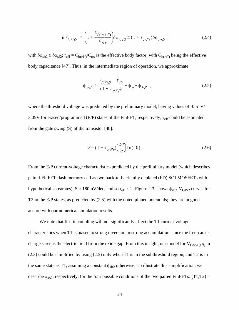
, (2.4)
with δφsb2 ≅ δφsf2; reff = Cb(eff)/Cox is the effective body factor, with Cb(eff) being the effective
body capacitance [47]. Thus, in the intermediate region of operation, we approximate
, (2.5)
where the threshold voltage was predicted by the preliminary model, having values of -0.51V/
3.05V for erased/programmed (E/P) states of the FinFET, respectively; reff could be estimated
from the gate swing (S) of the transistor [48]:
. (2.6)
From the E/P current-voltage characteristics predicted by the preliminary model (which describes
paired-FinFET flash memory cell as two back-to-back fully depleted (FD) SOI MOSFETs with
hypothetical substrates), S ≅ 180mV/dec, and so reff ~ 2. Figure 2.3. shows φsb2-VGfS2 curves for
T2 in the E/P states, as predicted by (2.5) with the noted pinned potentials; they are in good
accord with our numerical simulation results.
We note that fin-fin coupling will not significantly affect the T1 current-voltage
characteristics when T1 is biased to strong inversion or strong accumulation, since the free-carrier
charge screens the electric field from the oxide gap. From this insight, our model for VGbS1(eff) in
(2.3) could be simplified by using (2.5) only when T1 is in the subthreshold region, and T2 is in
the same state as T1, assuming a constant φsb2 otherwise. To illustrate this simplification, we
describe φsb2, respectively, for the four possible conditions of the two paired FinFETs: (T1,T2) =
δVGfS2 1Cb eff( )Cox
---------------------+⎝ ⎠⎜ ⎟⎛ ⎞
δφsf2 1 reff+( )δφsb2≅=
φsb2
VGfS2 Vt2–
1 reff+( )------------------------------- φc φFB+ +≅
S 1 reff+( ) kTq
------⎝ ⎠⎛ ⎞ 10( )ln∼
24

(E,E), (E,P), (P,E), and (P,P). As plotted in Fig. 2.4, when T1 is in the subthreshold region, for
states (E,E) and (P,P), T2 is also in the subthreshold region, and hence φsb2 is defined by (2.5); for
state (E,P), T2 is, for practical operation of the cell, in the strong-accumulation region, and φsb2 =
(φFB - φc) = -0.1V; and for state (P,E), T2 is, for practical operation of the cell, in the strong-
inversion region, and φsb2 = (φFB + φc) = 0.7V.
From our physical insight on the fin-fin coupling, we thus see that the paired-FinFET flash
memory cell can be characterized as two IGFETs, with effective back gate biases (VGbS1(eff), and
VGbS2(eff) defined analogously) dependent on the state of the adjacent transistor. The cell
subcircuit model, illustrated in Fig. 2.5, has six terminals: the common gate (G = Gf1 = Gf2), the
common (bulk-Si) body (B = B1 = B2), the left-FinFET (T1) drain (D1) and source (S1), and the
right-FinFET (T2) drain (D2) and source (S2); VGbS1(eff) and VGbS2(eff) are defined internally, as
described above, for the four different (T1,T2) conditions.
The paired-FinFET flash cell model, accounting for the fin-fin charge coupling, is defined
by four UFDG/Spice3 subcircuits: FLASHCELLEE, FLASHCELLEP, FLASHCELLPE, and
FLASHCELLPP. The four subcircuits account for the four possible (T1,T2) conditions of the
paired FinFETs, i.e., states (E,E), (E,P), (P,E) and (P,P), defining VGbS1(eff) and VGbS2(eff)
accordingly as described in the previously. There are two IGFETs in each subcircuit, modeled
with UFDG. The model was used to predict the IDS-VGS characteristics at VDS = 0.8V of the left
FinFET (T1), thus emulating a read operation. Simulation results predict the fin-fin coupling
effect: a larger Vt variation between (E,E) and (E,P) than that between (P,E) and (P,P), as
illustrated in Fig. 2.6., in good accord with the numerical simulation results in [49]. This results
prove that our model give accurate modeling of the fin-fin coupling effect.
The UFDG model is process/physics-based, involving only physical and structural
parameters [45]. The parameter evaluation thus can be done systematically, based on knowledge
25

of the transistor technology and underlying physics. Thus, for model calibration, only a few key
parameters need to be tuned via specific device measurements, as exemplified and explained
below.
The front gate-oxide thickness ‘TOXF’ is the equivalent oxide thickness (EOT), defined by
the dielectric stack (3.85nm/6.25nm/6.95nm ONO). To derive TOXF, the nitride thickness t2 is
converted to an equivalent oxide thickness t2(eq). Then,
(2.7)
where t1 and t3 are the respective oxide-layer thicknesses; (2.7) yields TOXF = 14nm for the stack
assumed.
The back gate-oxide thickness “TOXB” is the gap oxide thickness between the two fins.
The front-oxide fixed (normalized) charge density ‘NQFF’ (= Qox’/q at the SiO2-Si
interface) is a key parameter that distinguishes Vt of the programmed and erased transistors. It
effectively accounts for the actual charge density Qox stored at the N-O interface. With NQFF
calibrated to measured data, the nominal Qox for the programmed transistor was derived from
Qox’ as follows:
, (2.8)
where the calibration yielded NQFF = -5.0x1012cm-2; the factor of 2 in (2.8) is approximately
(t1+t2(eq)+t3)/(t1+t2(eq)), as derived from the EOT analysis.
The silicon fin-body of each FinFET also serves as the back gate of the adjacent transistor,
and so the back-gate work function “WKBG” is the work function of undoped silicon (with
natural acceptor doping density assumed to be ≅1015cm-3).
The front surface-state density ‘NSF’ is considered for the programmed status since the
TOXF EOT t1 t2 eq( ) t3+ += =
Qoxq
--------- 2Qox
′
q--------- 1.0– x10
13cm
2–≅ ≅
26

programming/erase processes seem to affect NSF, as reflected by a difference between the
measured subthreshold IDS-VGS slopes of the memory cell in the erased and programmed
statuses. NSF is inferred from the programmed device data, and is assumed negligible for the
erased device.
The body-source/drain junction recombination/generation current coefficient ‘JRO’ and the
drain and source parasitic series resistances ‘RD’ and ‘RS’ are tuned to match the measured Ioff
and Ion of the cells in a 32-cell string, respectively.
The subcircuit-cell model is verified by calibrations to measured IDS-VGS data obtained
from SAIT [49]. The measurement was conducted for a 32-cell string, with all the cells in the
string either in (E,E) or (P,P) state. Thus, we conduct the calibrations by simulating the 32-cell
VsNAND array read operation, which will be discussed in detail in next section. The calibration
results, showing model predictions in agreement with the measured data for programmed and
erased devices, are illustrated in Fig. 2.7.
2-3 Model Application
Since the model is process/physics based, the memory-cell model presented can be a useful
aid to device/technology design, and give reliable performance projections. To exemplify the
model utility, in this section, we introduce some of the model applications, i.e., to examine the
impact of process-parameter variations, to analyze the fin-fin charging coupling effect on Vt
variation, and to facilitate the circuit simulation of VsNAND FLASH array operation.
First, we use the model to check the sensitivities of Vt to variations in crucial process-
defined parameters. The model predicts IDS-VGS curves that reflect the Vt sensitivity of erased
and programed devices to variation in Lg, Wsi, and Qox’, as shown in Fig. 2.8. The model
predicts that the Vt variation in erased transistor is mainly due to variation in Si-fin thickness
and/or gate length, and that larger Vt variation in the programmed transistor is due to additional
27

sensitivity to variation in the charge density stored in the ONO structure.
Further, the model is used in fin-fin charge coupling analysis. The fin-fin coupling can
affect the integrity of paired-FinFET flash memory. A design modification for dealing with this
problem is to use a gap material with low dielectric constant, thereby ameliorating the coupling.
Our coupling model has been defined based on an SiO2 (oxide) gap, but it can be used for other
possible dielectrics as well, e.g., Si3N4 (nitride) and air [49]. For the other dielectrics, the gap
thickness (“TOXB” = tgap for oxide, where tgap is the physical dielectric thickness) is defined to
be the equivalent back-oxide thickness (EOT); for nitride, EOT = 0.52tgap, and for air, EOT =
3.9tgap. The model predicts, correctly, that the nitride gap yields the most coupling, while the air
gap yields the least coupling, consistent with the fact that thicker EOT reduces the coupling. The
predicted Vt variations caused by the fin-fin charge coupling for the programmed and erased
states, with oxide, nitride, and air gaps, are tabulated in Table 2.1. All the predictions agree
reasonably well with corresponding results of numerical simulations in [49].
The UFDG-based paired-FinFET flash memory cell model predicts the erased/
programmed transistor current-voltage characteristics accurately, including sensitivities to
process-induced parameter variations and fin-fin charge coupling. We now demonstrate its utility
in simulations of VsNAND-array read operations. Numerical simulation is not able to used in
this simulation because of the too much time consuming because of multi devices needs to be
simulated simulatneouly.A schematic of (32-bit) VsNAND string is illustrated in Fig. 2. 9. This
string has the same schematic as the one used in measurement. In the schematic, the two
FinFETs included in one subcircuit model are in different bit lines. Because the bit-line pitch is
below the design rule, it is impossible to make individual contact to each bit line [10]. Therefore,
the two bit lines share one contact and serve as a common bit line (CBL). There are two pairs of
select transistors, the string-select-line (SSL) transistors and the ground-select-line (GSL)
28

transistors, in the string. They have nearly the same structure as the memory cell, but having a
larger gate length. Subcircuit model for these 170nm select transistors is calibrated. In this string,
the signals to and from the two bit lines are not separated as shown in the figure.
As mentioned in section 2.2, VsNAND array read simulation was conducted for calibration
and verifying the cell model. The array simulation based on the compact model predicts the CBL
current (ICBL) subject to a word-line voltage sweep, i.e., the ICBL-VWL31 characteristics
governed by the FinFETs in the last word line (WL31) at VCBL=0.8V, for the conditions (E,E)
and (P,P) of the two paired FinFETs in the cell. A Vread (=6.0V) bias is applied to the other word
lines to ensure that all the other transistors are turned on. Simulation results agree well with
measured IDS-VGS data.
Further, we use the UFDG-based cell model to simulate the memory operations of the
string, e.g., Best On-Cell Current (with cell on WL31 selected and erased and all unselected cells
erased with their WLs at Vread), Worst On-Cell Current (with cell on WL31 selected and erased,
and all unselected cells programmed with their WLs at Vread), and Off-Cell Current (with cell on
WL00 selected and worst-case programmed, and all unselected cells erased with their WLs at
Vread). The model predicts the (DC) CBL current versus VCBL that reflects the state of (i.e., the
bit in) a selected cell. Simulation results of are tabulated in Table 2.2. As an example, figure
2.10. shows the predicted Worst On-Cell Current versus VCBL for different values of Vread and
VCSL set at 0.1V. The predictions generally conform well to measured data [50].
It is noted that the VsNAND-Array operation differs from those of conventional planar
type memory because of the fin-fin coupling effect. It is noted that by utilizing a VsNAND string
with two pairs of SSL transistors which can separate the two bit line, we can sensed the cell in
the four possible (T1,T2) conditions.
29

2-4 Model Extension
Besides charge trapped type, floating gate (poly silicon) is another alternative for the
Paired-FinFET flash memory design. Our model could still accounts for the floating-gate flash
memory pretty well, with only one parameter “TOXF” redefined. For the floating-gate memory,
The ONO dielectric stack is replaced by three layers: Inter-Poly Oxide, Poly Floating Gate and
Tunneling Oxide sequentially. Then,
, (2.9)
where t1 and t2 are the respective oxide-layer thicknesses. And the actual charge density Qox
stored at the Floating Gate for the programmed transistor could be derived from the “NQFF” (=
Qox’/q at the SiO2-Si interface) as follows:
. (2.10)
2-5 Summary
A UFDG-based subcircuit model for the paired-FinFET flash memory (VsNAND) cell,
taking into account the fin-fin charge coupling, was proposed, defined and verified. The model
accurately predicted the sensitivities to process-induced parameter variations and the fin-fin
charge coupling. The subcircuit model was used to successfully simulate the VsNAND-array
(string) operations, predicting correct values of Best On-Cell Current, Worst On-Cell Current and
Off-Cell Current. Finally, we noted that the model is easily extended to be applicable to the
floating-gate flash. In conclusion, the compact physics/process-based model is useful for
checking and analyzing the signal margins and process sensitivities for the VsNAND FLASH
array, as well as for aiding the paired-FinFET design.
TOXF EOT t1 t2+= =
Qoxq
---------Qox
′
q---------
t1 t2+
t2------------------
⎝ ⎠⎜ ⎟⎛ ⎞
×≅
30

Table 2-1. Model-predicted Vt variation between the erased states, (E,E) and (E,P), and that between the programmed states, (P,E) and (P,P), for oxide, nitride, and air gaps.
Gap MaterialΔVt
(Erased State)ΔVt
(Programmed State)
Oxide 0.37V 0.09V
Nitride 0.57V 0.18V
Air 0.11V 0.03V
Table 2-2. Model-predicted Best On-Cell Current, Worst On-Cell Current and Off-Cell Current with Vread=6.0V and VCSL=0V.
VCBL(V)Best On Cell Current(μA)
Worst On Cell Current(μA)
Οff Cell Current (nA)
0 0.00 0.00 0.00
1.0 2.07 1.57 1.25
2.0 3.04 2.42 73.6
31

Oxide/Nitride/Oxide(ONO)
n+ PolyOxideSilicon
hSi
wSi
wgap
Figure 2-1. Paired-FinFET flash memory (VsNAND) cell structure.
32

Oxide/Nitride/Oxide(ONO)
n+ PolyOxideSilicon
Figure 2-2. Illustration of the back-to-back IGFET structure of the paired-FinFET flash memory cell.
Left FinFET (T1)
Gate Oxide Body Oxide Gate
GateOxideBodyOxideGate
Right FinFET(T2)
33

Erased State
Programmed State
Figure 2-3. Simplified model-predicted back-surface potential in T2 (or T1) versus the frongate-source voltage, for the erased and programmed states of T2 (or T1).
-5.0 -4.0 -3.0 -2.0 -1.0 0.0 1.0 2.0 3.0 4.0 5.0-1.0
-0.5
0.0
0.5
1.0
VGfS2 (V)
Slope=1/(1+reff)≅0.33
φ sb2
(V)
34

Figure 2-4. Effective back-gate bias of T1, versus the front gate-source voltage of T2, as defined in the fin-fin coupling model for the four possible conditions of the paired FinFETs: (T1,T2) = (E,E), (E,P), (P,P), and (P,E). We assumed here that VGbS1 = 0, and hence VGbS1(eff) = φsb2.
VGfS2 (V)
VG
bS1(
eff)
(V)
-5.0 -4.0 -3.0 -2.0 -1.0 0.0 1.0 2.0 3.0 4.0 5.0-3.0
-2.0
-1.0
0.0
1.0
2.0
3.0
(E,E) (E,P) (P,E) (P,P)
35
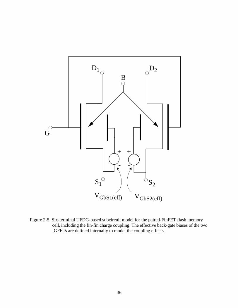
Figure 2-5. Six-terminal UFDG-based subcircuit model for the paired-FinFET flash memory cell, including the fin-fin charge coupling. The effective back-gate biases of the two IGFETs are defined internally to model the coupling effects.
G
BD2D1
S1 S2
VGbS2(eff)VGbS1(eff)
+ +
- -
36

Figure 2-6. Model-predicted current-voltage curves for the paired-FinFET flash memory cell in the four possible conditions: (T1,T2) = (E,E), (E,P), (P,P) and (P,E). Note here that VGS = VGfS1 = VGfS2.
-5.0 -4.0 -3.0 -2.0 -1.0 0.0 1.0 2.0 3.0 4.0 5.0VGS(V)
10-12
10-11
10-10
10-9
10-8
10-7
10-6
10-5
10-4
I DS(
A)
(E,E) (E,P) (P,E) (P,P)
37

Figure 2-7. Model-predicted ICBL-VWL31 curves (bold black) for the 32-cell paired-FinFET flash memory string, erased (Vt < 0) and programmed (Vt > 0) devices, compared with measured data (light curves/points); VDS = 0.8V, with source and body grounded.
38

-5.0 -4.0 -3.0 -2.0 -1.0 0.0 1.0 2.0 3.0 4.0 5.0
VGS (V)
10-11
10-10
10-9
10-8
10-7
10-6
10-5
I DS
(A)
IDS vs. VGS for erased and programmed status
Figure 2-8. Model-predicted IDS-VGS curves for the paired-FinFET flash memory cell, erased (Vt < 0) and programmed (Vt > 0) devices, showing composite Vt sensitivity to varying process-defined parameters; VDS = 0.8V. For the erased device, Lg and wSi were varied +/-10%. For the programmed device, Lg and wSi were varied the same, and NQFF was varied by about +/-7%.
39
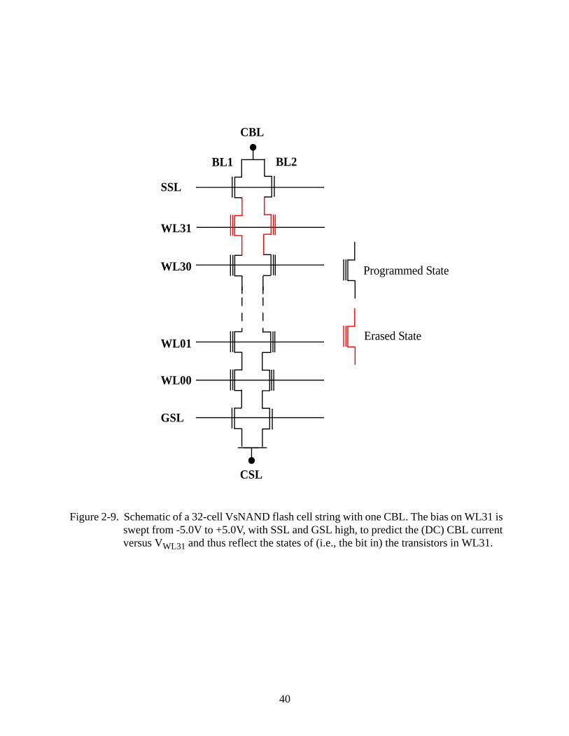
Figure 2-9. Schematic of a 32-cell VsNAND flash cell string with one CBL. The bias on WL31 is swept from -5.0V to +5.0V, with SSL and GSL high, to predict the (DC) CBL current versus VWL31 and thus reflect the states of (i.e., the bit in) the transistors in WL31.
SSL
WL31
WL30
WL01
WL00
GSL
CSL
Programmed State
Erased State
BL2BL1
CBL
40
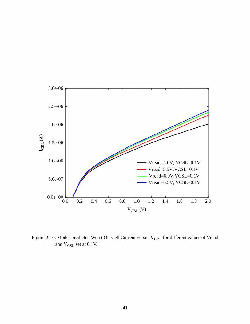
Figure 2-10. Model-predicted Worst On-Cell Current versus VCBL for different values of Vread and VCSL set at 0.1V.
0.0 0.2 0.4 0.6 0.8 1.0 1.2 1.4 1.6 1.8 2.0VCBL (V)
0.0e+00
5.0e-07
1.0e-06
1.5e-06
2.0e-06
2.5e-06
3.0e-06
I CB
L (A
)
Vread=5.0V, VCSL=0.1VVread=5.5V,VCSL=0.1VVread=6.0V,VCSL=0.1VVread=6.5V, VCSL=0.1V
41

CHAPTER 3PHYSICAL INSIGHTS ON THE MEMORY MARGIN OF SCALED (FULLY DEPLETED)
FLOATING-BODY 1T-DRAM CELLS
3-1 Introduction
Because of the integration problems associated with the storage capacitor of conventional
1T/1C DRAM in sub-50nm CMOS technology, interest in capacitorless 1T DRAM, i.e., floating-
body cells (FBCs) on SOI, has grown in recent years [19][20][23]-[28]. The FBCs are based on
sensing the MOSFET channel current, corresponding to the threshold voltage (Vt) which depends
on the floating-body charge condition effected via carrier generation or recombination during the
write processes. While FBCs emerged initially as partially depleted (PD) SOI MOSFETs [19],
two fully depleted (FD) devices with more potential scalability, i.e., the planar thin-BOX FD/SOI
MOSFET [25]-[27] and the quasi-planar double-gate (DG) Si FinFET [20][23][28], are more
promising candidates for FBCs linked to future nanoscale CMOS, especially for high-density and
embedded applications. The thin BOX enables the FD/SOI device to function as an FBC with
relatively low substrate bias for creating the accumulation layer at the back surface of the body,
which is necessary for effective charge storage and data sensing [29]. We assume that the DG
FinFET is on thin BOX too, and operates with low substrate bias for accumulation as well [23],
[28], as opposed to the independent-gate mode [20] (which is, electrically, equivalent to the FD/
SOI FBC) that necessitates more complex processing.
In this paper, we study, via both 2-D and 3-D numerical device simulations using Taurus
[51], whether acceptable memory, or current-signal, margins can be achieved in the two noted FD
FBCs as they are scaled to nanoscale gate lengths (Lg). This is tantamount to examining the
dependence of the signal margins on the ultra-thin-body (UTB) thickness (tSi), which must be
scaled with Lg to control short-channel effects (SCEs) [52][53][54]. We find that both devices
suffer significant signal-margin loss as tSi is scaled down, implying a scaling limit of 1T-DRAM
42

FBCs. We present new physical insights on the scaling, and explain the different reasons for the
margin losses in the two devices.
3-2 Thin-BOX FD/SOI FBC
We first examine the current-signal margin of thin-BOX FD/SOI FBCs via 2-D numerical
simulations using Taurus. The basic structure of the n-channel device is shown in Fig. 3.1. For the
simulations, we assume Lg = 56nm with an EOT of tox = 2nm, a midgap work-function gate, an
undoped UTB with tSi varying from 6nm to 35nm, a thin BOX with tBOX = 10nm, and a p+ Si
substrate (which facilitates the needed back-surface accumulation in the body). For nominal tSi
thin enough to control SCEs (≅Lg/4 for thin-BOX CMOS logic [54], which could be relaxed some
for the FBC application), we note that Vt is high (≅0.7V) when the substrate is biased for the
needed strong hole accumulation [54]. The memory-operation word-line (WL) and bit-line (BL)
biases used in the simulations, which are typical [25]-[26], are given in the inset of Fig. 3.2; a
typical read/write pulse time of 10ns is assumed. The substrate bias (Vsub = -2.0V) is fixed for
strong accumulation at the back of the UTB (when tSi in nominal). For write ‘1’, the WL (VGS) is
raised to induce a channel, and the BL (VDS) is pulsed high to drive channel current (IDS) and
induce impact-ionization current (IGi) to charge the body. For write ‘0’, the WL is raised and the
BL is pulsed down to forward-bias the B-D junction and discharge the body. The different
charged and discharged conditions in the body define, in the read operations, a body-voltage
variation (ΔVBS) which causes a Vt variation [9],
(3.1)
where r is the body coefficient, nominally defined by the device geometry [9]:
(3.2)
where Cb = εSi/tSi, Cox = εox/tox; εSi/εox ≅ 3 has been assumed.
ΔVt rΔVBS–=
r Cb Cox⁄ 3tox tSi⁄≅=
43
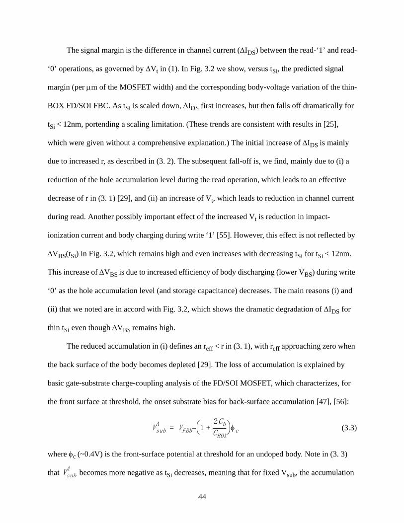
The signal margin is the difference in channel current (ΔIDS) between the read-‘1’ and read-
‘0’ operations, as governed by ΔVt in (1). In Fig. 3.2 we show, versus tSi, the predicted signal
margin (per μm of the MOSFET width) and the corresponding body-voltage variation of the thin-
BOX FD/SOI FBC. As tSi is scaled down, ΔIDS first increases, but then falls off dramatically for
tSi < 12nm, portending a scaling limitation. (These trends are consistent with results in [25],
which were given without a comprehensive explanation.) The initial increase of ΔIDS is mainly
due to increased r, as described in (3. 2). The subsequent fall-off is, we find, mainly due to (i) a
reduction of the hole accumulation level during the read operation, which leads to an effective
decrease of r in (3. 1) [29], and (ii) an increase of Vt, which leads to reduction in channel current
during read. Another possibly important effect of the increased Vt is reduction in impact-
ionization current and body charging during write ‘1’ [55]. However, this effect is not reflected by
ΔVBS(tSi) in Fig. 3.2, which remains high and even increases with decreasing tSi for tSi < 12nm.
This increase of ΔVBS is due to increased efficiency of body discharging (lower VBS) during write
‘0’ as the hole accumulation level (and storage capacitance) decreases. The main reasons (i) and
(ii) that we noted are in accord with Fig. 3.2, which shows the dramatic degradation of ΔIDS for
thin tSi even though ΔVBS remains high.
The reduced accumulation in (i) defines an reff < r in (3. 1), with reff approaching zero when
the back surface of the body becomes depleted [29]. The loss of accumulation is explained by
basic gate-substrate charge-coupling analysis of the FD/SOI MOSFET, which characterizes, for
the front surface at threshold, the onset substrate bias for back-surface accumulation [47], [56]:
(3.3)
where φc (~0.4V) is the front-surface potential at threshold for an undoped body. Note in (3. 3)
that becomes more negative as tSi decreases, meaning that for fixed Vsub, the accumulation
VsubA
VFBb 12CbCBOX----------+⎝ ⎠
⎛ ⎞– φc=
VsubA
44
level decreases.
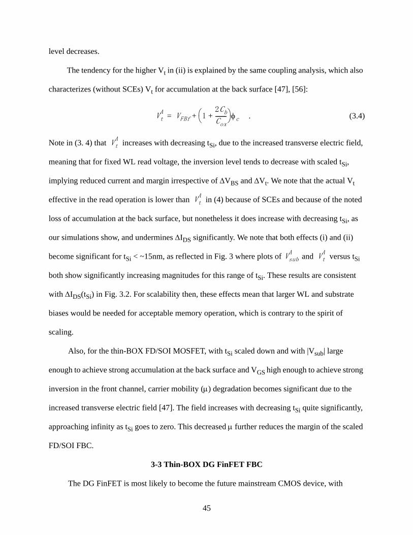
The tendency for the higher Vt in (ii) is explained by the same coupling analysis, which also
characterizes (without SCEs) Vt for accumulation at the back surface [47], [56]:
. (3.4)
Note in (3. 4) that increases with decreasing tSi, due to the increased transverse electric field,
meaning that for fixed WL read voltage, the inversion level tends to decrease with scaled tSi,
implying reduced current and margin irrespective of ΔVBS and ΔVt. We note that the actual Vt
effective in the read operation is lower than in (4) because of SCEs and because of the noted
loss of accumulation at the back surface, but nonetheless it does increase with decreasing tSi, as
our simulations show, and undermines ΔIDS significantly. We note that both effects (i) and (ii)
become significant for tSi < ~15nm, as reflected in Fig. 3 where plots of and versus tSi
both show significantly increasing magnitudes for this range of tSi. These results are consistent
with ΔIDS(tSi) in Fig. 3.2. For scalability then, these effects mean that larger WL and substrate
biases would be needed for acceptable memory operation, which is contrary to the spirit of
scaling.
Also, for the thin-BOX FD/SOI MOSFET, with tSi scaled down and with |Vsub| large
enough to achieve strong accumulation at the back surface and VGS high enough to achieve strong
inversion in the front channel, carrier mobility (μ) degradation becomes significant due to the
increased transverse electric field [47]. The field increases with decreasing tSi quite significantly,
approaching infinity as tSi goes to zero. This decreased μ further reduces the margin of the scaled
FD/SOI FBC.
3-3 Thin-BOX DG FinFET FBC
The DG FinFET is most likely to become the future mainstream CMOS device, with
VtA
VFBf 12CbCox--------+⎝ ⎠
⎛ ⎞ φc+=
VtA
VtA
VsubA
VtA
45
excellent scalability to the end of SIA ITRS [1]. There are two possible modes of FinFET-based
FBC operation. One is the independent-gate (IG) mode [20], with one gate biased for
accumulation, which, electrically, is the same device as the thin-BOX FD/SOI FBC that we
examined in Sec. II. This FinFET mode seems less viable for embedded-memory applications due
to its technology complexity and incompatibility with the CMOS logic. The other mode is the DG
FinFET on thin BOX with substrate bias [23], [28] for accumulation at the bottom of the fin, as
shown in Fig. 3.3. This mode, with simpler technology, is a more promising alternative for future
nanoscale 1T-DRAM FBCs. The FBC memory operation for this mode depends on a 2-D
floating-body effect, by which the accumulation layer at the bottom of the fin-body enables the
charge storage and the data sensing via sidewall-channel current dependent on the stored charge.
For the latter mode, we assume a DG (n-channel) FinFET analogous to the FD/SOI
MOSFET we assumed: Lg = 56nm, tox = 2nm, midgap gates, undoped fin-UTB with tSi varying
from 14nm to 42nm, tBOX = 10nm, and p+ Si substrate; we initially assume a fin height (or device
width) hSi = 56nm, but will check its effect on the 2-D floating-body effect later. We examine the
device via 3-D numerical device simulations using Taurus, and give predicted currents per μm of
hSi. For nominal tSi thin enough to control SCEs (≅Lg/2 [53], which could be relaxed for FBCs),
we find, as reflected by the predicted IDS-VGS characteristics in Fig. 3.5, that Vt is slightly higher
when the (p+) substrate is biased for strong accumulation (Vsub = -2.0V) than it is (≅φc [47]) for
depletion in normal logic operation (with a grounded, lightly doped substrate). The higher Vt (by
≅30mV for this case) results from a 2-D gate-substrate charge-coupling effect by which the hole
accumulation at the bottom of the fin increases the electric field in the sidewall channels. The
increased field also causes some mobility degradation as evident in Fig. 3.5. This same 2-D
coupling effect underlies reff for this FinFET FBC, and since it seems to be mild, we might
surmise that reff is low and the memory margin is inferior to that of the planar FD/SOI FBC in
46

which the coupling effect is 1-D and stronger.
The predicted current-signal margin of the DG FinFET FBC, and the corresponding body-
voltage variation, versus tSi are shown in Fig. 3.6, along with the WL and BL voltage pulses used
(with 10ns read/write times) for the simulations. Indeed, for nominal tSi, ΔIDS is smaller than that
of the FD/SOI FBC, even with two gates, and it decreases as tSi is scaled down. Like for the FD/
SOI FBC, the ΔIDS decrease is uncorrelated with ΔVBS, but it is not as abrupt like for the FD/SOI
cell; it begins for relatively thick tSi, and it increases gradually with decreasing tSi. These
ΔIDS(tSi) results are consistent with a relatively low reff defined by the 2-D floating-body effect,
which is not as strong as the 1-D effect reflected by (2). Since the coupling effect on Vt is small
(see Fig. 3.5), we can deduce that the margin reduction for scaled tSi is due mainly to loss of the
hole accumulation, which is easily explained. For thin tSi, the 2-D electric field induced by the
sidewall gates near the bottom of the fin tends to induce depletion/inversion there [57], thereby
reducing the accumulation level and suppressing its effect on Vt; the 2-D reff is decreased. A lack
of DG FinFET-FBC scalability is clearly implied, and perhaps more so than that for the FD/SOI
FBC.
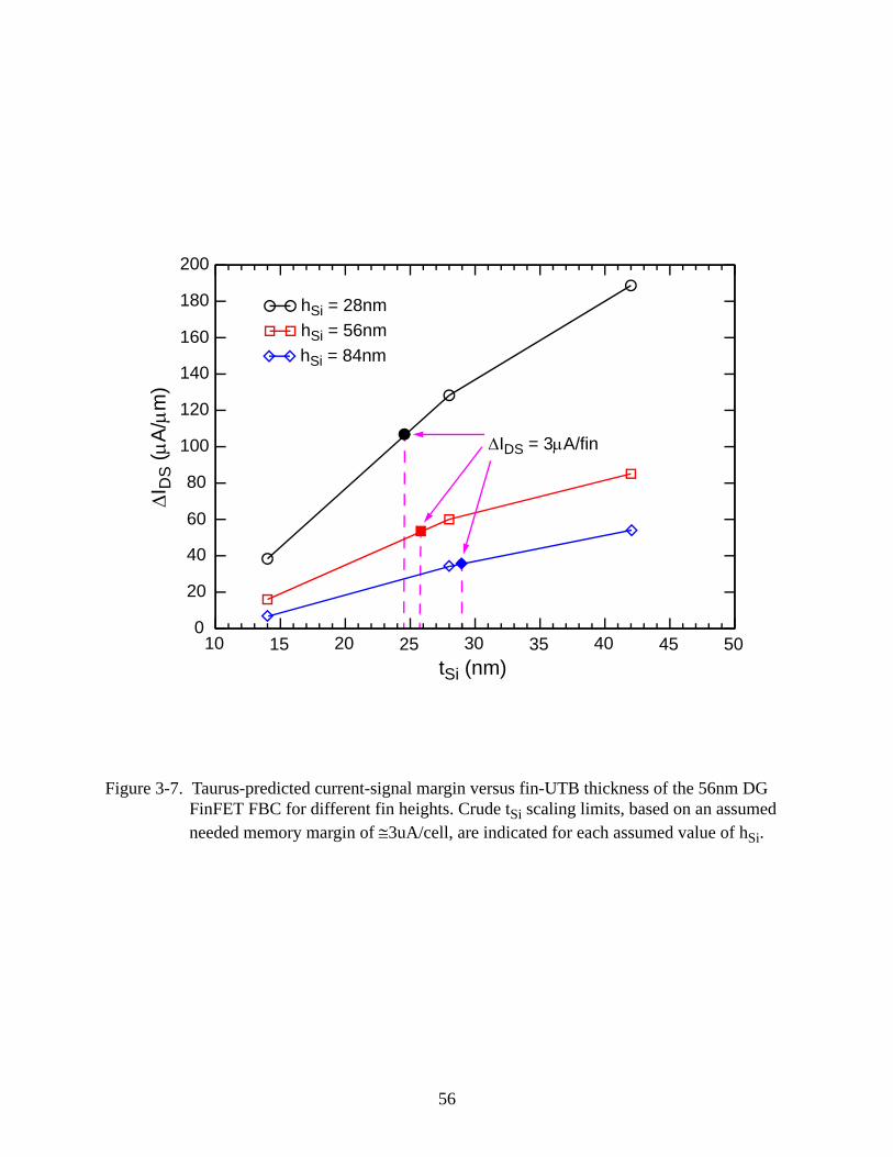
We have assumed hSi = 56nm (=Lg) for our study of the DG FinFET FBC. Since the cell
performance is based on a 2-D coupling effect in the fin-body, we now check whether varying hSi
could improve the margin and the scalability of the cell. A quasi-2-D extension of (3. 2) suggests
that increasing hSi would diminish the coupling and reff, yielding reduced margin. Decreasing hSi
would enhance the coupling, but, based on our insight derived in Sec. II, would exacerbate the
margin loss for scaled tSi; a more abrupt fall-off of ΔIDS would result. These insights are borne out
by the simulation results in Fig. 3.7 showing ΔIDS versus tSi for three different values of hSi. No
significant scaling benefit is revealed
47
3-4 Summary
The memory-margin dependences on UTB thickness of nanoscale planar thin-BOX FD/SOI
and quasi-planar DG FinFET 1T-DRAM cells were examined via 2-D and 3-D numerical device
simulations, and physical insights were attained. We found that the FD/SOI FBC suffers from
abrupt current-signal margin degradation with UTB scaling because of loss of body accumulation
charge, as well as loss of inversion charge due to increased threshold voltage. Further, thin tSi,
with the needed accumulation, yields high transverse electric field, which leads to mobility
degradation and additional loss of margin. We noted also that the DG FinFET FBC suffers from
nominally low signal margin due to a relatively low, 2-D effective body coefficient, as well as
gradual margin loss with fin-UTB scaling due to loss of accumulation charge at the base of the
fin. Both 1T-DRAM cells hence seem to have limited scalability.
Although scaling tSi of the two FD FBCs we examined is clearly limited, the Lg scalability
is not as clear. (In this discussion, Lg is actually the effective channel length, which is longer than
the gate length when gate-source/drain underlap [52]-[54] is used in the device design.) The
margin predictions for the FD/SOI FBC in Fig. 3.2 indicate a tSi scaling limit of ~10nm with good
margin, which would translate to Lg ~ 40nm for the CMOS but could imply a shorter Lg limit for
the FBC, depending on the SCE tolerance. For shorter Lg and Vt lowered due to SCEs, the
required WL holding (negative) voltage would tend to be larger in magnitude, and this
requirement could define the practical Lg scalability. However, based on SCE sensitivity to tSi
[52], the Lg limit would not be much shorter than the noted 40nm. Further, use of a thicker tSi for
the FBC than that used for the scaled CMOS would complicate the technology for the embedded-
DRAM application. The achievable margin of the DG FinFET FBC will be nominally lower, and,
as indicated by the predictions in Fig. 3.6, acceptable (≅50μA/μm is assumed, based on a ≅3μA/
fin (i.e., per cell) need [27]) down to a tSi scaling limit of only ~25nm; this translates to Lg ~ 50nm
48

for the CMOS, but perhaps somewhat shorter for the FBC as noted for the FD/SOI cell. And,
whereas the predictions in Fig. 3. 7 show a tendency for improvement in the scalability of the
FinFET FBC with decreasing hSi, the benefit is not significant and such design would complicate
the embedded-DRAM technology since the CMOS hSi should be as high as possible. Thus, the
two FD 1T-DRAM cells seem to have comparable scalability, which, unfortunately, is not close to
the end of the SIA ITRS (e.g., Lg < 10nm for high-performance CMOS logic [1]).
49
Si Substrate
BOX
n+ n+p-
Gate
tSi
G (word line)
(bit line)(source line)DS
Sub
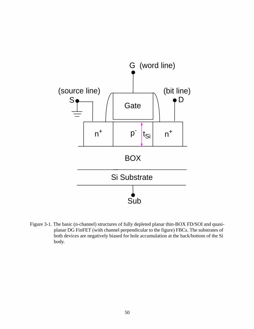
Figure 3-1. The basic (n-channel) structures of fully depleted planar thin-BOX FD/SOI and quasi-planar DG FinFET (with channel perpendicular to the figure) FBCs. The substrates of both devices are negatively biased for hole accumulation at the back/bottom of the Si body.
50

Write ‘1’ Write ‘0’ Read
WL 1.0V 1.0V 1.0V
BL 1.5V -1.0V 0.2V
tSi (nm)
ΔVB
S (V)
ΔI D
S (μ
A/μm
)
0 10 20 30 400
20
40
60
80
100
120
140
160
180
200
220
0 5 10 15 20 25 30 35 400.2
0.3
0.4
0.5
0.6
0.7
0.8
0.9
1
Figure 3-2. Taurus-predicted current-signal margin and body-voltage variation versus UTB thickness of the 56nm FD/SOI FBC. The word-line and bit-line voltage pulses used for the 2-D transient memory-sequence simulation are indicated in the inset, and 10ns read/write times were assumed; Vsub = -2.0V. ΔIDS is defined as the difference between IDS at the ends of the read-‘1’ and read-‘0’ operations; ΔVBS is defined as the difference in VBS (i.e., the quasi-Fermi-potential separation at the source side of the body) between the two read operations.
51
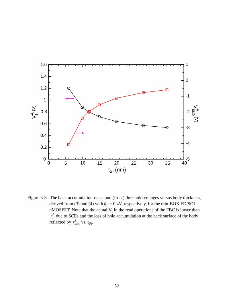
Figure 3-3. The back accumulation-onset and (front) threshold voltages versus body thickness, derived from (3) and (4) with φc = 0.4V, respectively, for the thin-BOX FD/SOI nMOSFET. Note that the actual Vt in the read operations of the FBC is lower than
due to SCEs and the loss of hole accumulation at the back surface of the body reflected by vs. tSi.VtA
VsubA
0 10 20 30 400
0.2
0.4
0.6
0.8
1
1.2
1.4
1.6
0 5 10 15 20 25 30 35 40-5
-4
-3
-2
-1
0
1
VA t(V
) VAsub
(V)
tSi (nm)
52

Figure 3-4. The basic (n-channel) structures of fully depleted planar thin-BOX FD/SOI and quasi-planar DG FinFET (with channel perpendicular to the figure) FBCs. The substrates of both devices are negatively biased for hole accumulation at the back/bottom of the Si body.
Gate
SiO2
Si Substrate
BOX
Si Fin
tSi
Sub
53

Vsub = 0.5VVsub = -2.0V
VGS (V)
VDS = 50mV
0 0.1 0.2 0.3 0.4 0.5 0.6 0.7 0.80
50
100
150
200
250
300
ΔI D
S (μ
A/μm
)
Figure 3-5. Taurus-predicted current-voltage characteristics of the 56nm DG nFinFET, for tSi = 28nmn and hSi = 56nm, with the (p+) substrate biased for strong accumulation (-2.0V) and for depletion (0.5V, which is equivalent to a grounded, lightly doped substrate) at the base of the fin. For the latter case, Vt ≅ φc, whereas it is ≅30mV higher for the former case.
54

Write ‘1’ Write ‘0’ Read
WL 0.8 V 0.8 V 0.8 V
BL 1.5 V -1.0 V 0.2 V
tSi (nm)
ΔI D
S (μ
A/μ
m)
ΔVB
S (V)
10 20 30 40 500
10
20
30
40
50
60
70
80
90
100
10 15 20 25 30 35 40 45 500
0.1
0.2
0.3
0.4
0.5
0.6
0.7
0.8
0.9
1
Figure 3-6. Taurus-predicted current-signal margin and body-voltage variation versus fin-UTB thickness of the 56nm DG FinFET FBC. The word-line and bit-line voltage pulses used for the 3-D transient memory-sequence simulation are indicated in the inset, and 10ns read/write times were assumed; Vsub = -2.0V.
55
tSi (nm)
ΔI D
S (μ
A/μ
m)
hSi = 28nmhSi = 56nmhSi = 84nm
10 15 20 25 30 35 40 45 500
20
40
60
80
100
120
140
160
180
200
ΔIDS = 3μA/fin
Figure 3-7. Taurus-predicted current-signal margin versus fin-UTB thickness of the 56nm DG FinFET FBC for different fin heights. Crude tSi scaling limits, based on an assumed needed memory margin of ≅3uA/cell, are indicated for each assumed value of hSi.
56

CHAPTER 4PHYSICAL INSIGHTS ON BJT-BASED 1T CAPACITORLESS DRAM
4-1 Introduction
Because of the integration limit of conventional 1T/1C DRAM in nanoscale CMOS
technology, interest in “capacitorless” 1T DRAM cells on SOI, which utilize the MOSFET
floating body to store data, has grown in recent years [20][24]25][29]. While most conventional
1T DRAM cells work through sensing of the channel current, dependent on the threshold voltage
that varies with the floating-body charge condition, a recently reported 1T DRAM cell utilizes the
parasitic BJT current in the SOI MOSFET structure for both writing and reading data [30]-[34].
This BJT-based 1T DRAM cell has attracted interest because of its full compatibility with
standard SOI processing and its potentially supreme performance, e.g., very high signal margin,
low power consumption, and high density. The BJT-based DRAM cell is also shown to have
better scalability and compatibility than conventional FD-MOSFET DRAM cells because it can
be effected with FinFETs without independent gate bias or substrate bias. Although the parasitic
BJT has already been studied intensively as one of the floating-body effects in the SOI MOSFET
[60][61], there is not much insight on how it is used for DRAM operation and why a FinFET can
work without an independent gate.
In this chapter, using numerical device simulations, we physically overview the basic
operation of BJT-based 1T DRAM cells. We find and physically explain an interesting
phenomenon that renders the write-‘1’ operation extremely sensitive to a time offset between the
word-line (WL) and bit-line (BL) voltage pulses. We also gain insight concerning the role of gate
capacitance in the BJT-based charging process, which explains why a fully depleted (FD) cell,
e.g., a FinFET [32], can be effectively charged without an independent bias for accumulation
charge that is necessary in conventional FD-MOSFET DRAM cells [20]. We also reveal a bulk-
57

accumulation effect that undermines the BJT operation as the cell-body thickness is scaled.
Furthermore, we explore the viability of BJT-based DRAM by studying its sensitivity to
variations of process parameters, and retention time. Based on the physical insights we get, we
show that undoped, FD/SOI bodies/bases will be needed, as in SG-FD/SOI MOSFETs or DG
FinFETs. Further, we note that the serious hot-carrier reliability problems constitute the major
issue that threatens the viability of BJT-based DRAM. A capacitorless DRAM for a low-voltage
operation is called for.
4-2 Physical Insights on BJT-Based 1T DRAM Operation
The operation of the BJT-based DRAM cell, illustrated in Fig. 4.1 (with grounded S), is
based almost exclusively on the parasitic BJT of the floating-body SOI n-channel MOSFET,
which is driven to near the BVCEO breakdown for writing and reading ‘1’ (body/base charging).
The memory effect is shown by a programming/read window shown in Fig. 4.2. This ID (≅IBJT)
vs. VGread (WL pulse) plot is derived from transient (pulsed-VG) simulations done with Taurus
[51], for stored ‘1’ (charged body/base) and stored ‘0’ (uncharged body/base) states of a 90nm
PD/SOI cell. The detail description of memory operation, together with the now physical insight
we get about it will be shown later. The programming/read window shows a very high sense
margin mainly due to BJT latching. We also point out that IBJT increases some with the read VG
for state ‘1’. We believe this increase is due to BJT current gain (β) increasing with VGread due to
less bulk accumulation charge (and hence lower effective Gummel number) within the effective
thickness (tSi(eff)) of the BJT. Later, this effect will be discussed more and shown to be an
limitation of BJT-based dram scaling.
We first demonstrate the general BJT-based 1T DRAM-cell operation via 2-D numerical
device simulations done with Taurus [51]. We present results of simulating the DRAM operation
of a DG (n-channel) FinFET, as illustrated in the inset of Fig. 4.3. The FinFET has a 56-nm gate
58

length (Lg) with an EOT of tox=2nm, an undoped fin-body with thickness tSi=28nm, and midgap
gates; the default fin height, or gate width, is 1μm. As shown in Fig. 4.3, for write ‘1’, the BL
(VD) is pulsed to near the breakdown voltage (BVCEO [46]) of the parasitic BJT, and the WL (VG)
is pulsed up to raise the body/base voltage [VBS(t)], via capacitive coupling, enough to increase β
and drive the latch condition, β(M - 1) ≅ 1, where M is the impact-ionization multiplication factor.
The (weak) impact-ionization current that charges the body/base is IGi = (M - 1)IBJT, where IBJT is
the induced BJT current. For write ‘0’, VG is pulsed up again to raise VBS, and VD is kept well
below BVCEO, thus effecting removal of the stored holes by mainly body-source junction
recombination; IBJT(t) decays to zero. For the read operation, with high VD < BVCEO, a smaller
VG pulse is used, but high enough to induce BJT latch, via VBS(t) > 0, when the body is charged
(read ‘1’); when the body is not charged, VBS(t) is lower and no significant current is induced
(read ‘0’).
In Fig. 4.3, we show predicted current, IDS(t) ≅ IBJT(t), corresponding to a complete
sequential memory operation of the BJT-based DRAM cell for two different offsets (ΔtWB)
between the WL and BL voltage-pulse drops, ΔtWB=+1ns and ΔtWB=-1ns as indicated. We see an
interesting phenomenon. For ΔtWB=+1ns, i.e., the BL voltage begins to fall 1ns after the WL
voltage, the predicted operation is normal with a high current margin about 450μA/μm. However,
for ΔtWB=-1ns, no current is sensed for the ‘1’ state, implying a failure of write ‘1’. Since latched-
BJT currents are seen in the write-‘1’ process for both cases, the different charging results must be
defined during the short 2ns difference in ΔtWB. This insight is confirmed by the predicted
ultimate peak hole density (pw1) in the body/base, under the gate oxide, plotted in Fig. 4.4. versus
ΔtWB. The stored hole density is quite sensitive to ΔtWB; pw1 increases by a factor of five as ΔtWB
increases from -1ns to +1ns. We note that when ΔtWB=-1ns, pw1 is clearly smaller than the critical
density (pcrit) for latch, even approaching the density (pw0) corresponding to stored ‘0’. This
59

means that the write-‘1’ process in this case virtually results in write ‘0’. Note also in Fig. 4.4 that
ΔtWB=0 yields tenuous results (i.e., pw1~pcrit); indeed, a finite WL-BL pulse offset is essential.
The ΔtWB phenomenon can be explained by considering the basic charging process in a
floating-body 1T DRAM cell. For hole storage, the floating body needs a substantive intrinsic
dynamic capacitor [29]. We find that the gate capacitance (CG) serves as the predominant charge-
storage element in BJT-based charging, but its efficacy depends on ΔtWB. When the BJT is
latched in the write-‘1’ process, VG is irrelevant; the “open-base” BVCEO breakdown is self-
sustaining [46]. Thus, for ΔtWB>0, i.e., when the WL pulse drops prior to the BL pulse, the BJT
remains latched, with VBS(t) nearly fixed, when VG drops negative to hold the data, as shown in
Fig. 4.3. Then, the latched BJT charges CG with additional holes, ΔQp ≅ CGΔVG where ΔVG is
the drop in VG. However, for ΔtWB<0, i.e., when the BL pulse ends prior to the WL pulse, the BJT
unlatches when VD drops, and holes in the base/body are quickly removed by recombination in
the forward-biased source and drain junctions. Then, there is no way to charge CG when WL
ultimately drops. This insight reveals that the effective body, or CG, charging occurs during the
(positive) offset time. It further implies that, since the BJT latch can be achieved very fast due to
the positive feedback, a very short write-‘1’ time is possible. Additional simulations confirm this
implication, predicting effective times of less than 5ns. Also, we note that the utilization of CG for
the charge storage is a unique property of the BJT-based cell, and enables the memory operation
with FD bodies. For example, an undoped FinFET could be used [31], without an independent
bias to induce accumulation in the body as needed in conventional 1T DRAM cells for storing
holes and reading data [20], [24], [29]. For the latter cells, in which channel current drives the
impact ionization, CG cannot be used as the storage element because of the existence of the
channel.
60

4-3 Bulk-Accumulation Effect on Scalability of BJT-Based 1T DRAM
As mentioned, in the write-‘1’ process with ΔtWB>0, the BJT remains latched during the
offset time. However, the current decreases a bit when VG drops, as indicated in Fig. 4.3. This is
because of the added charge ΔQp on CG, which manifests as bulk accumulation charge in the
body. The hole accumulation tends to deactivate the BJT near the surfaces, or to reduce the
effective thickness [tSi(eff)] of the BJT base, and hence undermine the BJT and memory
operations. We also note this tSi(eff) effect when we introduce the generic programming/read
window previously. This bulk-accumulation effect thus portends a scaling limitation. As tSi is
scaled with the technology, tSi(eff) shrinks, ultimately pinching-off the BJT. Additional simulation
results in Fig. 4.4 illustrate this issue. For the Lg=56nm cell (in the working ΔtWB≅+1ns region),
the write-‘1’ process is successful, even as tSi is thinned; in fact, pw1 actually increases a bit
because of reduced junction recombination after the BL drop. However, for a scaled cell with
Lg=28nm and tSi scaled accordingly (~Lg/2), the hole density is dramatically reduced, and more
so as tSi is thinned. The write-‘1’ process is very sensitive to the assumed small tSi variation of
only 2nm. This extreme sensitivity, and the undermining of the write-‘1’ process, reflects the
reduction of tSi(eff); ultimately, the process fails as the BJT is not latched and CG is not charged.
The scaling problem is emphasized in Fig. 4.5, which shows predicted read-‘1’ and write-
‘1’ currents versus tSi for the Lg=28nm cell. Note how the read-‘1’ current falls off dramatically
with tSi, thus diminishing the margin; the current is virtually zero for tSi≤13nm. Whereas our
prediction of this trend is valid, the actual tSi limit noted could vary with the WL and BL voltage
pulses used, as well as with differences in the numerical model parameters [51] assumed. The
write-‘1’ current is less sensitive because the higher VG yields less bulk accumulation. We
propose that the bulk-accumulation effect could be controlled by not scaling tSi so much when Lg
is scaled for higher memory density, since short-channel effects are not too significant for the
61

DRAM cell.
4-4 Viability of BJT-Based 1T DRAM
Since BJT-based DRAM cell is driven to near the BVCEO breakdown in the write ‘1’ and
read ‘1’ operations, its high sensitivities to variations in crucial process-defined parameters are
expected. We checked these sensitivities of a 90nm PD/SOI dram cell via 2-D numerical
simulations with Taurus [51]. We assumed a typical retrograded channel doping density, with NBL
= 5x1017cm-3 near the surface and NBH = 1018cm-3 below the depletion layer, of thickness tb =
40nm; we let the SOI thickness be tSi = tf = 120nm. The simulating results show that both the
high- and low-doped portions of the body/base contribute to the BJT action. We show Taurus-
predicted shifts of current for write ‘1’ and read ‘1’ due to variations in Lg, tb, tf, NBL, and NBH in
Table 4.1 respectively. The results show high sensitivity of memory operation to these expected
parameter variations, especially in Lg and NBH. This is because Lg is the virtual base width of the
parasitic BJT, which determines β directly, and the predominant part of the BJT is in the lower,
quasi-neutral part of the body, where NBH defines the Gummel number.
It is noted that our process/physics-based compact model for partially depleted (PD) SOI
MOSFETs, UFPDB [62], can be used to simulate the operation of BJT-based PD/SOI DRAM cell
in Spice3, as shown in Fig. 4.6. Thus, we also use the UFPDB to check the BJT-based PD/SOI
DRAM cell’s sensitivies to variations in process-related parameters. The UFPDB-predicted shifts
of current for write ‘1’ and read ‘1’ due to variations in Lg, tb, tf, NBL, and NBH are shown in
Table 4.2. Although the sensitivities seem to be overestimated by UFPDB, their predicted
significances are in accord with the Taurus predictions.
Because of the significant random fluctuations in the body/base doping, the PD/SOI
memory cell will suffer substantive sensitivity degradation when scaled down, just like the widely
varying threshold voltage of the scaled PD/SOI MOSFET. As shown in Table 4.1, Taurus predicts
62

significant write-‘1’ and read-‘1’ current shifts (>20%) with the assumed variations in NBH and
NBL. These variations will be larger and random in scaled PD/SOI, and so the results in Table 4.1
imply that PD/SOI memory cell will not be viable in the future. Undoped, FD/SOI bodies/bases
will be needed, as in SG-FD/SOI MOSFETs or DG FinFETs.
The ‘0’-retention time subject to BL disturb by GIDL current is another important issue that
threatens BJT-based cell’s viability. Since a high VDS is used in BJT-based DRAM cell to achieve
a BJT latch, the associated BL disturb becomes more serious than that in conventional FBC.
Although a long underlap (~30nm) has been suggested for BJT-based cell to solve this ‘0’-
retention problem [32], it not only increases cell area but also degrades its memory compatibility
for embedded application.
Further, BJT-based DRAM cells suffers significant hot-carrier reliability issues due to the
high drain voltages (VDS) required for BJT latch [63][64]. A endurance failure after only 500
cycles for BJT-based FinFET DRAM cell has been shown in [63]. Therefore, this hot-carrier
reliability problem is the fatal issue that threatens BJT-based cell’s viability. A lower VDS
operation is necessary for the capacitorless DRAM cells to achieve a high reliability.
4-5 Summary
The basic operation of BJT-based 1T DRAM cells on SOI was simulated numerically, and
physical insights were derived. We noted that the gate capacitance is the predominant charge-
storage element, implying that fully depleted bodies without independent biasing for
accumulation charge can be used. We noted and explained that a positive WL-BL offset (ΔtWB) is
necessary for effective write ‘1’, with extreme sensitivity to ΔtWB. Sensitivity to the needed ΔtWB
must be accounted for in the circuit design. We noted a bulk-accumulation effect that may
undermines the BJT and cell operations for thin tSi, resulting in loss of current margin and
ultimate write-‘1’ failure. Considering sensitivities to process parameters, we proposed that PD/
63

SOI is not viable as scaling down, while FD body device, such as FD/SOI or FinFET, will be
needed in the future. We noted that the serious hot-carrier related reliability problems, due to the
high VDS for BJT latch is the major issue that threatens the viability of the BJT-based DRAM. A
viable capacitorless DRAM cell must be able to operate at a low VDS for enough reliability.
64

Table 4-1. Taurus-predicted write-‘1’ and read-‘1’current sensitivities of the 90nm PD/SOI Gen2 cell to typical variations in process-defined structural parameters.
ΔIwrite ‘1’ ΔIread ‘1’
Lg
(-10% / +10%)+14% / -19% +15% / -22%
tb(-10% / +10%)
-5.0% /+3.0% -7.5% / +4.7%
NBL
(-10% / +10%)+5.2% / -3.5% +4.9% / -4.3%
NBH
(-10% / +10%)+11% / -7.7% +14% / -12%
tb(-20% / +20%)
-8.3% / +7.0% -12% / +8.8%
NBL
(-20% / +20%)+10% / -8.3% +9.8% / -8.4%
NBH
(-20% / +20%)+22% / -15% +28% / -23%
65
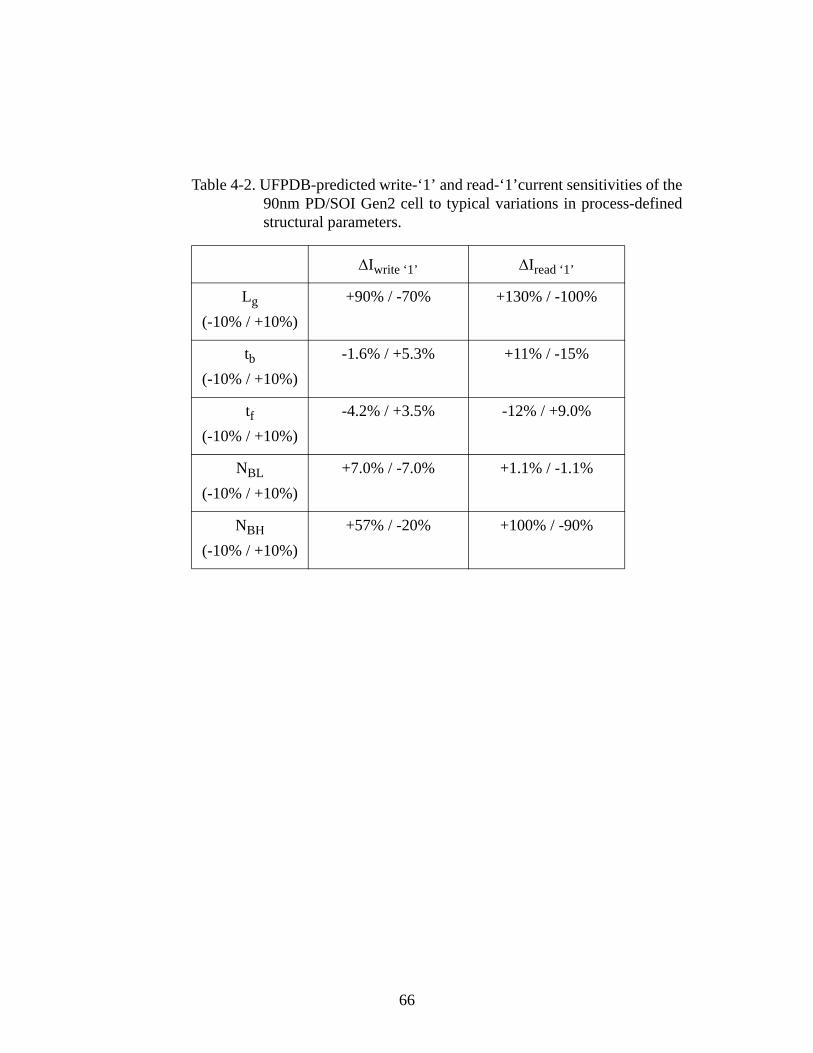
Table 4-2. UFPDB-predicted write-‘1’ and read-‘1’current sensitivities of the 90nm PD/SOI Gen2 cell to typical variations in process-defined structural parameters.
ΔIwrite ‘1’ ΔIread ‘1’
Lg
(-10% / +10%)+90% / -70% +130% / -100%
tb(-10% / +10%)
-1.6% / +5.3% +11% / -15%
tf(-10% / +10%)
-4.2% / +3.5% -12% / +9.0%
NBL
(-10% / +10%)+7.0% / -7.0% +1.1% / -1.1%
NBH
(-10% / +10%)+57% / -20% +100% / -90%
66
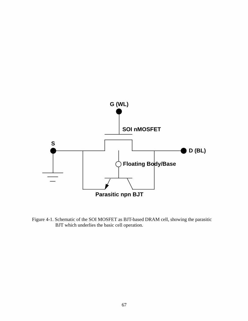
Figure 4-1. Schematic of the SOI MOSFET as BJT-based DRAM cell, showing the parasitic BJT which underlies the basic cell operation.
D (BL)
G (WL)
SOI nMOSFET
Parasitic npn BJT
Floating Body/Base
S
67

Figure 4-2. Taurus-predicted BJT-based DRAM programming/read window for the 90nm PD/SOI MOSFET/BJT.
-2.0 -1.5 -1.0 -0.5 0.0VGread (V)
VG(w)VG(r)
-100
0
100
200
300
400
500
600
700
I D (μ
A/μ
m)
-200
State ‘1’
State ‘0’
ΔV=0.8V
68
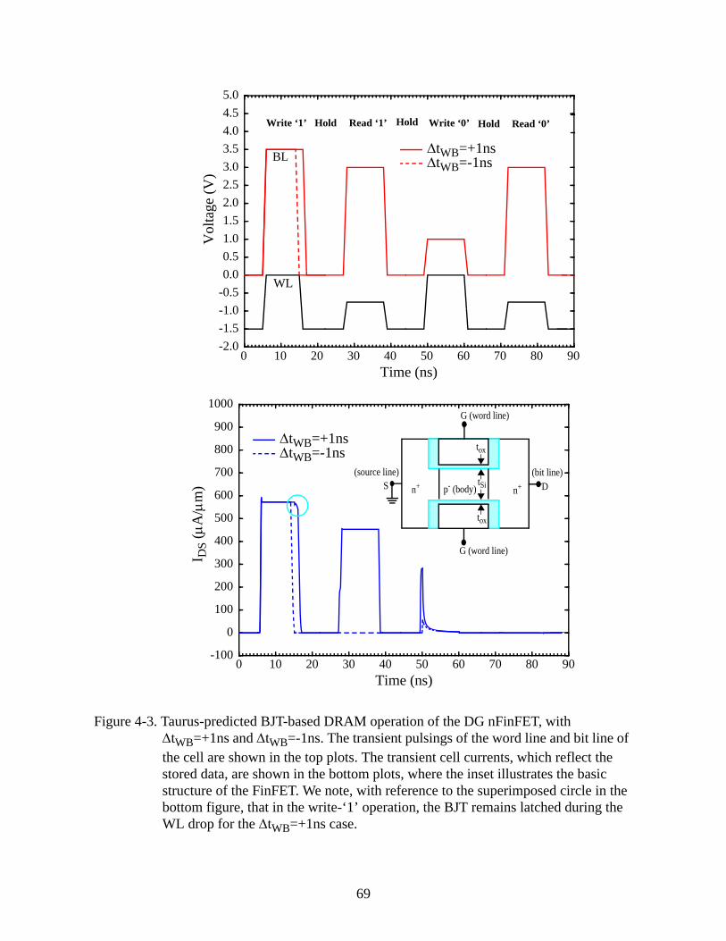
BL
WL
Vol
tage
(V)
-2.0-1.5-1.0-0.50.00.51.01.52.02.53.03.54.04.55.0
0 10 20 30 40 50 60 70 80 90Time (ns)
Write ‘1’ Hold Read ‘1’ Hold Write ‘0’ Hold Read ‘0’
ΔtWB=+1nsΔtWB=-1ns
0 10 20 30 40 50 60 70 80 90-100
0
100
200
300
400
500
600
700
800
900
1000
n+ n+p- (body) D S
G (word line)
G (word line)
tox
tox
tSi(bit line)
Time (ns)
I DS
(μA
/μm
)
(source line)
ΔtWB=+1nsΔtWB=-1ns
Figure 4-3. Taurus-predicted BJT-based DRAM operation of the DG nFinFET, with ΔtWB=+1ns and ΔtWB=-1ns. The transient pulsings of the word line and bit line of the cell are shown in the top plots. The transient cell currents, which reflect the stored data, are shown in the bottom plots, where the inset illustrates the basic structure of the FinFET. We note, with reference to the superimposed circle in the bottom figure, that in the write-‘1’ operation, the BJT remains latched during the WL drop for the ΔtWB=+1ns case.
69
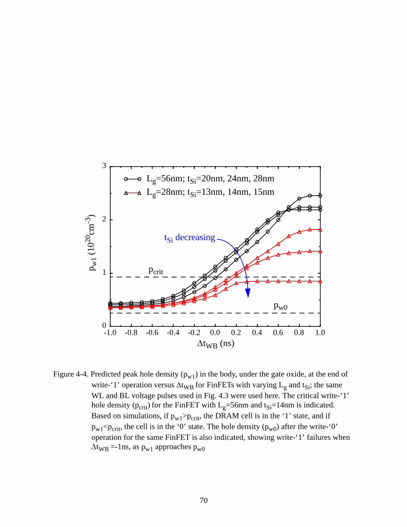
-1.0 -0.8 -0.6 -0.4 -0.2 0.0 0.2 0.4 0.6 0.8 1.0ΔtWB (ns)
0
1
2
3
p w1 (
1020
cm-3
)
tSi decreasing
pcrit
pw0
Lg=56nm; tSi=20nm, 24nm, 28nmLg=28nm; tSi=13nm, 14nm, 15nm
Figure 4-4. Predicted peak hole density (pw1) in the body, under the gate oxide, at the end of write-‘1’ operation versus ΔtWB for FinFETs with varying Lg and tSi; the same WL and BL voltage pulses used in Fig. 4.3 were used here. The critical write-‘1’ hole density (pcrit) for the FinFET with Lg=56nm and tSi=14nm is indicated. Based on simulations, if pw1>pcrit, the DRAM cell is in the ‘1’ state, and if pw1<pcrit, the cell is in the ‘0’ state. The hole density (pw0) after the write-‘0’ operation for the same FinFET is also indicated, showing write-‘1’ failures when ΔtWB =-1ns, as pw1 approaches pw0
70
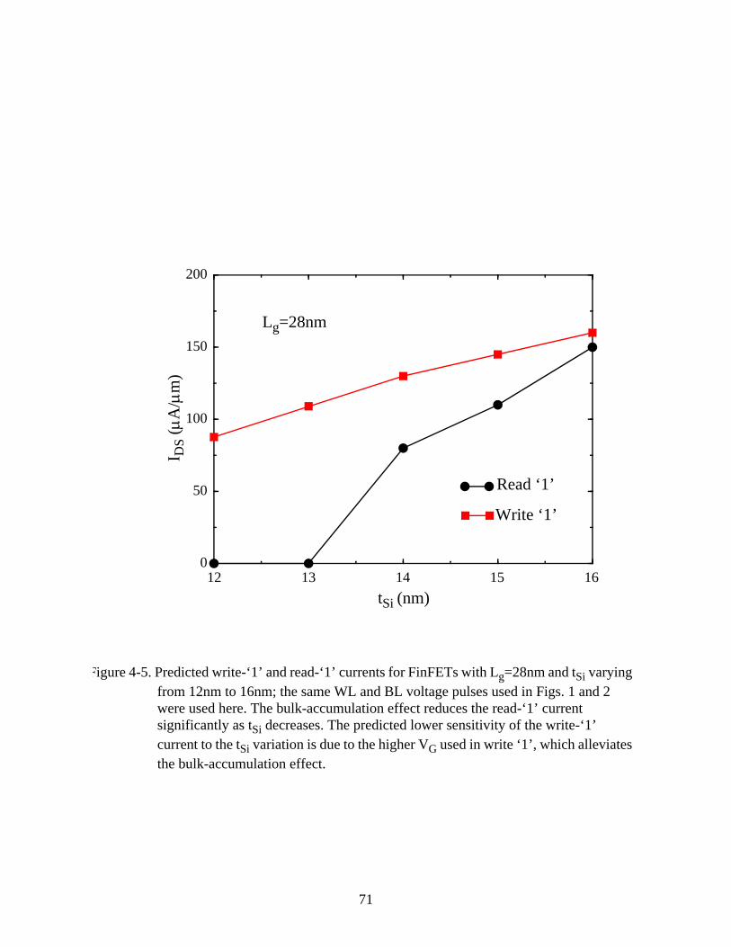
Figure 4-5. Predicted write-‘1’ and read-‘1’ currents for FinFETs with Lg=28nm and tSi varying from 12nm to 16nm; the same WL and BL voltage pulses used in Figs. 1 and 2 were used here. The bulk-accumulation effect reduces the read-‘1’ current significantly as tSi decreases. The predicted lower sensitivity of the write-‘1’ current to the tSi variation is due to the higher VG used in write ‘1’, which alleviates the bulk-accumulation effect.
0
50
100
150
200
Read ‘1’
Write ‘1’
tSi (nm)12 13 14 15 16
Lg=28nm
I DS
(μA
/μm
)
71

Time (ns)
I DS
(μA
/μm
)
Figure 4-6. UFPDB -predicted BJT-based DRAM operation of the 90nm PD/SOI nMOSFET
-3
-2
-1
0
1
2
3
4
5
Bia
s (V
)
0 10 20 30 40 50 60 70 80 90Time (ns)
Bit line Word line
Write ‘1’ Read ‘1’ Write ‘0’ Read ‘0’
0 10 20 30 40 50 60 70 80 90-200
0
200
400
600
800
1000
1200
Write ‘1’ Read ‘1’ Write ‘0’ Read ‘0’
72

CHAPTER 5A PUNCH THROUGH-BASED 2T DG-FINFET FBC
5-1 Introduction
Because of the process difficulties associated with the storage capacitor of conventional 1T/
1C DRAM in sub-50nm CMOS technology, capacitorless DRAM cells, i.e., SOI floating-body
cells (FBCs), have attracted intensive research interest in recent years [20][24][25][30-32]. The
first kind of FBC works through sensing of the channel current, which is dependent on the
threshold voltage that varies with the floating-body charge condition. Either channel impact-
ionization current or GIDL current has been used to charge the floating body. However, as
demonstrated in Chapter 3, 1T FBCs lack scalability due to loss of sense margin caused by scaled
body thickness. Furthermore, the independent gate or substrate bias [which is required for charge
storage and data sensing for fully depleted (FD) cells] not only limits the memory compatibility
for embedded applications but also reduces the effective body coefficient (reff) significantly as the
FBC scales down [65]. Another kind of FBC, analyzed in Chapter 4, utilizes the parasitic BJT
current in the SOI MOSFET for both write and read. This cell has drawn more attention recently
because it provides high sense margin, non-destructive read, and, especially, superior
compatibility without the need of any substrate or independent gate bias. However, as discussed
in Chapter 4, BJT-based FBCs , as well as the 1T FBCs [66], suffer from hot-carrier reliability
issues due to the high drain voltage (VDS) required for impact ionization and BJT latch (>2.5V).
While both of the two noted FBCs consist of one transistor, the 2T FBGC is also promising
[59][67]. FBGC utilizes the floating body of one transistor to directly drive the gate of the second
transistor. It offers excellent memory performance including high sense margin and very long
retention times, although the gated-diode structure of the first transistor (T1) increases the process
complexity. In addition, in order to achieve a long ‘0’ retention time under BL disturb, T1 needs a
73

very long underlap (~30nm) which not only increases cell area but also degrades its memory
compatibility.
In this chapter, we propose a novel punch through (PT)-based 2T FinFET FBC that offers
low power operation, high sense margin, long worst-case retention times, improved reliabilities,
and good compatibility for embedded memory applications in future nanoscale CMOS
technology. This PT-based FinFET FBC utilizes GIDL for programming and PT current for data
sensing, without the need for substrate or independent gate bias. The proposed FBC design
enables a low VDS (~1V) operation, which, as a result, improves the reliability by avoiding hot-
carrier effects (HCE). We provide physical insights on the mechanism of the modulation of PT
current by floating-body charge conditions in the FinFET-based FBC. We also find that the PT-
based memory effect strongly depends on the thickness of the FinFET body. We design a PT-
based FinFET FBC in a 2T structure by adding another pass transistor to block BL disturb for
holding data. We show that the 2T structure also plays an important role in achieving a high
Iread‘1’/Ihold ‘1’ ratio for viable DRAM array operation, which is hard to achieve in a 1T PT-based
FinFET FBC. Furthermore, we verify the functionality of the PT-based FBC for planar thin-BOX
FD/SOI MOSFET technology. However, we find that, compared with its counterpart using
FinFET technology, the thin-BOX FD/SOI FBC suffers from a lower sense margin due to its
finite body capacitance.Thus, 2T thick-body FinFETs seem to be the best candidates for the PT-
based FBC. Thorough performance comparisons of the PT-based 2T FinFET FBC with other 1T
and 2T FBCs are made in the final section.
5-2 PT-Based Memory Effect in a FinFET FBC
In this section, we focus on the basic PT-based memory effect in DG-FinFET FBCs. The PT
phenomenon is well known as a major obstacle for submicron CMOS transistor scaling [68].
However, there are some devices, for instance, PT transistors [69-71], that utilize gate-controlled
74

PT current for high-voltage and high-frequency applications. In addition, it has been reported that
when a short-channel MOSFET is biased with high VDS, the avalanched holes can trigger not
only the parasitic BJT latch but also PT current, which can be used for memory application [72].
However, this cell works almost the same as the BJT-based FBC [30], and so it also suffers from
serious HCE issues due to the BJT latch. While our PT-based FinFET FBC works through sensing
of only the charge-modulated PT current rather than BJT current, it can operate at a remarkably
low VDS (~1V) and achieve superior reliability.
We first demonstrate the basic DRAM operation of a one-transistor (1T) PT-based FinFET
FBC via numerical simulation using SenTaurus [73]. The 2T FBC architecture suggested for
performance improvement will be discussed later in detail in the next section. The basic structure
of the n-channel DG FinFET is shown in Fig. 5.1. For the simulation, we assume Lg=56nm with
an EOT of tox =3nm, a midgap work-function gate, an undoped body with tSi=56nm; the default
fin height, or gate width, is 1μm. Noted that a thicker body is used, compared with the nominal tSi
that is thin enough to control SCEs (~Lg/2 [53]). We will show later that this design is critical for
the PT-based FinFET FBC.
In Fig. 5.2, we present results of simulating the DRAM operation of the FinFET. The GIDL
tunneling current, controlled by the WL (VG) and the BL (VD) voltage pulses, is used to charge
the floating body, i.e., write a ‘1’. To write a ‘0’, VG is pulsed up to raise the body voltage (VB)
via capacitive coupling, thus effecting the removal of the stored holes by body-source/drain
recombination. This write-‘0’ process can be very efficient due to the strong capacitive coupling
in the PT-based FinFET FBC which has a negligible body capacitance. For the read operation, VG
is also pulsed up to raise VB to be high enough to turn-on the PT current when the body is charged
(read ‘1’); when the body is not charged, VB is lower and no significant PT current is induced
(read ‘0’). Since WL is negatively biased during programming and read operations, the gate
75
capacitance (CG) serves as the charge storage element so that no substrate or independent gate
bias is required. We show, also in Fig. 5.2, the predicted current, IDS(t), corresponding to a
complete sequential memory operation. Negligible programming power is predicted since there is
no channel current. The results, with nanoscale-second programming and read times, demonstrate
the basic operation of the cell, showing that stored charge can effectively modulate the PT current
even at low VD (1V), and yield a good signal margin (~53μA/μm).
The functionality of the PT-based FinFET FBC is further confirmed by the predicted
programming/read window (ΔVGS ~ 0.4V) in Fig. 5.3. This IDS vs. VGS (WL pulse) plot is
derived from transient (pulsed-VG) simulations of the read operation for stored-‘1’ and stored-‘0’
states. The predicted read-‘0’ current becomes significant only when VGS > -0.3V; this is mainly
the MOSFET subthreshold diffusion current (which is unusually high because of the relatively
severe SCEs in the PT-cell FinFET). The low Vt and large subthreshold slope (SS) are due to the
serious SCEs introduced by thick body. Contrarily, for reading ‘1’, as the VGS increases,
significant current occurs due to punch through when VGS ≥ −0.8V. For increasing VGS, the read-
‘1’ current is ultimately dominated by the MOSFET subthreshold current, as the read-‘0’ current
is, as implied by the disappearing read window in Fig. 5.3.
We find that the predicted read-‘1’ current follows the behavior of space-charge limited
current very well. Actually our PT-based FinFET FBC can be generally modeled by the current-
voltage relation for the gate-controlled punch-through transistor [69][71]:
(5.1)
where L is the channel length and A is the device cross-sectional area. In [69] and [71], VtPT is a
function of VGS. For our device, VtPT is also modeled as a function of VBS due to the stored-
charge modulation. As shown in Fig. 5.4, for the same biases as in the memory operation, the
IDS9εμA
8L3
------------- VDS VtPT VGS VBS( , )–[ ]2=
76

SenTaurus-predicted read-‘1’ current data follows (5.1) (with calibration) very well, further
confirming our conclusion that the read-‘1’ current is dominated by punch through.
Now we give a general physical explanation on the modulation of flow of PT current by the
stored charge in the floating body of the DG FinFET. The onset of the punch-through current
requires the body/source potential barrier (φbarrier) to be low enough for the electrons to be
injected from source into the body, where they drift to the drain via space charge-limited flow.
When the FinFET FBC is in the ‘1’ state, its high VB raised by the stored charged will reduce
φbarrier and turn-on the punch-through current. This is confirmed by the predicted potential
distribution of the FinFET FBC from source to drain, as plotted in Fig. 5.5 for both the ‘1’ and ‘0’
states. As shown in Fig. 5.5, φbarrier for the ‘1’ state is lower than that for the ‘0’ state, and leads to
the noted punch-through current for the ‘1’ state in Fig. 5.3. We also note in Fig. 5.5 that φbarrier
for the thick-body FinFET (tSi=56nm) is much lower than that for a thin-body FinFET
(tSi=28nm). The lower φbarrier in thick-body FinFET is due to DIBL. This insight implies that the
thin-body FinFET with higher φbarrier is not viable as a PT-based FBC, which is confirmed by
predicted results in Fig. 5.6 that show no functional programming/read window of the FinFET
(tSi=28nm). As shown in Fig. 5.6, the read-‘1’ and read-‘0’ current curves overlap with each
other, both being just the MOSFET subthreshold current. Compared with the thick-body FinFET,
the thin-body FinFET shows a higher Vt and lower SS since the DIBL is well controlled. The
enhanced DIBL effect in the thick-body FinFET plays a critical role in enabling a PT-based
DRAM operation, even at low VDS. Without the DIBL enabling, even though there are holes
stored in the floating thin body of the FinFET, no PT current can be triggered.
Thus, a thin-body FinFET can only work as a FBC in the BJT-based mode. We reiterate,
however, that the BJT-based read operation requires high VDS (>2.5V) for transistor latch. Since
the parasitic BJT current gain (β) in the MOSFET is very small (~30 for the thin-body FinFET
77

FBC), high VBS (> 0.8V) is needed to get sufficient (hole) current margin for the BJT-based read
‘1’. As a result, a high VDS for strong impact ionization and BJT latch is needed to maintain this
high VBS, otherwise the current will decay very quickly due to significant recombination current.
Since PT current mainly consists of the electron current (Ielectron/Ihole>105) for a thick-body
FinFET during read ‘1’), VBS in the PT-based read-‘1’ operation can be much lower than that in
the BJT-based read ‘1’. Thus, the PT-based read-‘1’ current will not decay too much during the
read operation, even without impact ionization. Additional simulations confirm this implication,
predicting only a 3% decrease of read-‘1’ current after 10 read-‘1’ operations.
As noted, a thick body is critical for the functionality of the PT-based FinFET FBC. This
could cause a read-‘0’ error. Since a large number of unselected hold-‘1’ cells and the intended
read-‘0’ cell share the same BL, to guarantee a valid read-‘0’ operation, the total hold-‘1’ leakage
current must be significantly smaller than the read-‘1’ current. Thus, the increased hold-‘1’
leakage current due to thick-body could be a serious problem for the viability of PT-based FinFET
FBC. Additional simulations predict a high hold-‘1’ leakage current (~0.1μA/μm) for the thick-
body 1T FinFET FBC, which implies that the number of cells that could share the same BL
should be less than 500 (i.e., < Iread ‘1’/I hold ‘1). Since typically there are 256 to 1024 cells on one
BL of a DRAM array [74], the viability of the PT-based 1T-FinFET (with thick body) memory
array could be limited.
Another problem with the PT-based DRAM cell is the short ‘0’ retention time due to
GIDL-based charging under BL disturb. Because GIDL current also serves as the major leakage
mechanisms for hold ‘0’ during BL disturb time, there is little design space to realize a fast GIDL-
based program and a long ‘0’ retention [67]. This short ‘0’ retention time associated with the
GIDL charging is a common problem for all FBCs using GIDL-based charging [59][75].
Further, note that in the memory operation in Fig. 5.2, the WL voltages used for writing ‘1’
78
and writing ‘0’ are different, which implies that row programming is not possible. In the next
section, we will propose a 2T structure for the PT-based FinFET FBC with new operation bias to
solve all the problems noted herein.
5-3 The PT-Based 2T FinFET FBC
The basic structure of PT-based 2T FinFET FBC is shown in Fig. 5.7. The cell comprises
two serially connected transistors, T1 and T2. T1 works the same as the PT-based 1T FinFET
FBC discussed in last section; T2 is a pass transistor that works as a switch controlled by a control
line (CL). T2 is turned on to pass BL voltage to T1 during programming and read operations, and
turned off to block the BL disturb to T1 when data is held. We assume T2 to have the same
structure as T1; the area penalty due to 2T structure is thus relieved since T1 and T2 can share a
common source/drain. To improve the switch performance of T2, we may design it with a thinner
body to control SCEs better. However, then the noted common source/drain can not be achieved
due to the difference of body thickness between T1 and T2; thus, more cell area is the cost.
Although the PT-based FBC utilizes FinFETs with thick bodies, its compatibility to logic FinFET
technology is not threatened too much. This is because with the vertical structure, the body
thickness of the FinFET is not determined by the planar SOI thickness; no additional processing is
needed for the thick-body device fabrication.
Fig. 5.8 shows a SenTaurus-simulated DRAM operation for this 2T FBC. Generally, the
memory operation is the same as what we assumed for the 1T cell, except for the added CL bias as
well as a new 2-phase WL pulse used for writing both ‘1’ and ‘0’. During the first phase of WL
pulse, WL is pulsed up to raise VBS and write a ‘0’. During the second phase, WL is pulsed down;
whether to write ‘1’ or to keep the ‘0’ state is determined by whether a 1V BL pulse is used. We
note that the duration of the first WL phase can be very short (~2ns) because write ‘0’ can be very
efficient for our cell. Although this 2-phase WL bias adds complexity to the memory circuit, the
79
same WL voltage can now be used for writing both ‘1’ and ‘0’, enabling row programming and
increasing the write speed while eliminating WL-disturb effects. The simulation predicts a
negligible current margin drop (~ 3μA) of the 2T FBC compared with that of the 1T cell, due to
only small channel resistance of T2 added in reading data.
As mentioned earlier, one of the motivations of the 2T cell design is to solve the short ‘0’
retention-time problem associated with BL disturb. The retention of the 2T FBC is expected to be
greatly improved by introducing the pass transistor T2, because it blocks the BL disturb to T1
when T1 is holding data. This is demonstrated by the simulation results in Fig. 5.9, which indicate
‘0’ retention times for the 1T and 2T FBCs under 1V continuous BL stress of 10μs and 20ms,
respectively. It is much easier to use continuos BL stress for checking the worst-case ‘0’ retention
than to use the actual pulsing BL disturb. However, we would like to stress that the ‘0’ retention
improvement of the 2T cell under actual, pulsing BL disturb could be more significant than that in
continuous BL stress. As illustrated in Fig. 5.10, when a continuous BL stress is applied to the 2T
FBC while holding ‘0’, the off current of T2 will charge the parasitic capacitance (CFN)
associated with the floating node (FN), until VFN, or VD of T1, rises to a quasi-steady level that is
determined by the ratio of the resistance of T1 and T2. This VFN induces GIDL current to charge
the floating body of T1. When a pulsing BL disturb is applied, as shown in Fig. 5.10, the off
current of T2 will charge CFN when the BL voltage is high, and discharge CFN when the BL
voltage is low. Thus, a smaller VFN and longer retention can be expected. Although it is too
computationally expensive to directly simulate the retention time under BL pulsing, we can
estimate it based on the simulation for continuous BL disturb. If we assume a BL pulse with 50%
duty cycle, then VFN could be evenly reduced by 50% compared with the value for continuous BL
disturb, if the ratio of the resistance of T1 and T2 in both cases are the same. Thus, we can
emulate the 1V BL-pulses disturb by assuming a 0.5V continuos BL stress. For the 1T FBC, since
80
the BL stress is applied to T1 directly, the new BL pulse with 50% duty cycle can only double the
‘0’ retention time of the continuous BL disturb case. The corresponding simulation results for
both cells are shown in Fig. 5.9. An improved ‘0’ retention time longer than 1s for the proposed
2T FBC under pulsing BL disturb is predicted. Even though there are uncertainties in the
modeling of the carrier generation and recombination that imply some equivocality in the
predicted retention time, the significant improvement of worst-case retention time due to the 2T
structure is doubtless.
In Section 5.2, we showed that the thick-body PT-based FinFET FBC suffers from high
hold-‘1’ leakage current that may cause a read-‘0’ error. This problem can also be solved by the
introduction of the 2T cell structure. With T2 blocking the high BL voltage being passed to T1,
the hold-‘1’ leakage current can be reduced significantly; the simulation results predict a 2.8nA/
μm for 2T versus 100nA/μm for 1T, which implies that more than 10000 2T cells can share one
BL than in the 1T FBC. Thus, the proposed 2T cell architecture is an ideal design for the PT-based
FinFET FBC, not only for long retention times but also for viable memory array realization.
5-4 PT-Based Thin-BOX FD/SOI FBC
Besides the DG FinFET, the thin-BOX FD/SOI MOSFET, illustrated in Fig. 5.11, is also a
promising candidate for future CMOS technology. In this section, we explore the application of
our PT-based FBC in this technology via numerical simulations using SenTaurus, and compare its
performance with the counterpart FinFET FBC. We first assume a 1T thin-BOX FD/SOI
MOSFET analogous to the FinFET we assumed: Lg=56nm, tox=3nm, midgap gates, undoped
UTB with tSi=38nm, and tBOX=10nm; the default gate width is 1μm. The cell has a thicker UTB
than the nominal tSi (~Lg/4 [54]) that is thin enough to control SCEs in a logic cell, in order to
have a strong DIBL effect for the PT-based memory effect.
The predicted memory operation of this FBC is shown in Fig. 5.12, where the transient
81

pulsings of WL and BL are the same as those for the FinFET-based cell in Fig. 5.2. However, we
find that, compared with the FinFET counterpart, the sense margin of thin-box FD/SOI FBC is
much lower: 13μA/μm vs. 53μA/μm. This can be explained by further analysis of the read-‘1’
operation, during which the WL pulse increases the body voltage via capacitance coupling. For
the FD/SOI FBC, the ultra-thin BOX brings in finite body capacitance which limits the increase
of VBS. By using a thick BOX, FD/SOI FBC exhibits a substantial sense margin increment; as
shown in Fig. 5.12, the sense margin of the FBC with 60nm BOX (29μA/μm) is much higher than
that for the 10nm-BOX cell. (It is noted that because of the worse SCEs in the thick-BOX FBC, a
thinner UTB (~29nm) was used to maintain a low-level read-‘0’ current.) Thus, the thick-BOX
FD/SOI MOSFET is more promising as a PT-based FBC.
However, since the body thickness of the planar FD/SOI MOSFET is the thickness of SOI,
fabricating the thick-body memory devices and the thin-body logic devices on the same chip
would require added processing steps. Thus, the PT-based planar FD/SOI FBC has a CMOS
compatibility disadvantage compared with the counterpart FinFET FBC.
Besides higher sense margin and better compatibility, the DG FinFET also has a better
GIDL-charging efficiency than that in the planar FD/SOI FBC. It has been reported that the GIDL
current in a <110> channel, as common in the FinFET, could be an-order-of-magnitude larger
than that in a <100> channel of a FD/SOI MOSFET [76]. Although this advantage of the FinFET
FBC is not reflected in our simulations, in which we assumed a <100> channel for both FinFET
and FD/SOI MOSFET, we can expect a shorter write-‘1’ time for the FinFET FBC.
5-5 Summary
A novel PT-based 2T DG-FinFET FBC for low VDS operation was presented, and its
memory operation was demonstrated and verified via numerical simulations. We noted that the
stored-charge in the floating body modulates the PT current via controlling φbarrier. We also noted
82

that the enhanced DIBL associated with thick body is critical for PT-based memory operation. We
designed a PT-based FBC with a 2T structure, which not only improves the worst-case ‘0’
retention time under BL disturb but also greatly reduces the hold ‘1’ leakage current for a viable
memory array. We also verified the functionality of a PT-based planar thin-BOX FD/SOI FBC.
However, this cell was also noted to suffer from low sense margin, relative to that of the FinFET
cell, as well as incompatibility with CMOS logic devices.
A performance comparison of our PT-based FinFET FBC has been made with other 1T or
2T FBCs in Table 5.1. Compared with 1T FBCs, our cell is not limited by the body factor r. It
does not require any substrate or independent gate bias. It also shows a reliability advantage by
using low VDS. Although our cell is larger in size, these performance advantages nonetheless
make it a promising FBC-memory competitor. Compared with the other 2T FBCs, i.e., FBGC
[66], our cell shows an obvious process compatibility advantage since it uses conventional CMOS
technology, while T1 in the FBGC is actually a gated diode with very long G-D underlap.
Although both cells consist of two transistors, our cell takes smaller area considering the common
source/drain of T1 and T2, as well as the long underlap used in FBGC. However, our cell uses a
two-phase write programming which is more complex than that in FBGC. In conclusion, our PT-
based 2T FinFET FBC could be one of the promising candidates for future capacitorless DRAM.
83

Table 5-1. Performance comparison among PT-based FinFET FBC, FBGC and 1T FBCs
II-based 1T FBC
GIDL-based 1T
FBC BJT-based 1T FBC
FBGC3 (2TFBC)
PT-based 2T FinFET
FBC
Sense Margin ~50μA ~30μA ~500μA ~80μA ~50μA
Retention Time
~25ms ~100μs ~800ms ~10s ~1s
Write Time ~10ns ~10ns <2ns ~10ns ~15ns
Cell Area 4F2 4F2 4F2 >8F2 8F2
Process com-plexity and
Compatability
like CMOS
like CMOS
Bad(Underlap)
Bad (Underlap
and P+ source)
like CMOS
Reliability like CMOS
like CMOS
Very Bad (hot car-
rier)
like CMOS
like CMOS
84
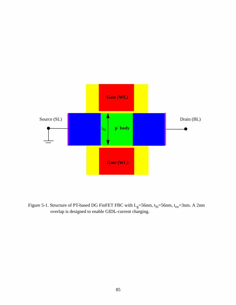
Figure 5-1. Structure of PT-based DG FinFET FBC with Lg=56nm, tSi=56nm, tox=3nm. A 2nm overlap is designed to enable GIDL-current charging.
Source (SL) Drain (BL)
Gate (WL)
Gate (WL)
tSi p- body
85

Figure 5-2. SenTaurus-predicted DRAM operation of PT-based DG FinFET FBC. The transient pulsings of the word line and bit line of the cell are shown in the top plots. The transient cell currents, which reflect the stored data, are shown in the bottom plots.
0 10 20 30 40 50 60 70 80Time (ns)
-3
-2
-1
0
1
2
-20-10
01020304050607080
Write ‘1’ Hold Read ‘1’ Hold Write ‘0’ Hold Read ‘0’
BL
WL
Vol
tage
(V)
0 10 20 30 40 50 60 70 80Time (ns)
I DS
(μA
/μm
)
Write ‘1’ Hold Read ‘1’ Hold Write ‘0’ Hold Read ‘0’
86

-1 -0.9 -0.8 -0.7 -0.6 -0.5 -0.4 -0.3 -0.2 -0.1 0 0.1VGS (V)
-50
0
50
100
150
200
250
I DS
(μA
/μm
)
0.2
‘1’ state ‘0’ state
Figure 5-3. SenTaurus-predicted read-‘1’ and read-‘0’ currents for FinFET FBC with Lg=56nm, tSi=56nm versus VGS; a functional programing/read window is shown.
FinFET w/ Lg=56nm tSi=56nm VDS=1V
87

Figure 5-4. SenTaurus- and model-predicted read-‘1’ currents of FinFET FBC versus VDS. The model is described by equation (5.1), in which the value of ‘VtPT’ is calibrated to be 0.2V and 0.41V when VGS=-0.5V and -0.6V respectively; ‘9εμA/L3’is calibrated to have a value of 156μA/V2.
0.6 0.7 0.8 0.9 1 1.1 1.2 1.3 1.4 1.5-50
0
50
100
150
200
250
300
Model SenTaurus
VDS (V)
I DS(
read
‘1’)
(μA
/μm
)
VGS=-0.5V, VtPT=0.2V
VGS=-0.6V, VtPT=0.41V
88

Figure 5-5. SenTaurus-predicted electric potential distribution in the center of the body of FinFET FBCs with tSi=56nm and tSi=28nm during read operations. The potential at source is set to be 0V as potential reference.
-80 -60 -40 -20 0 20 40 60 80-0.8
-0.6
-0.4
-0.2
0
0.2
0.4
0.6
0.8
1
1.2
read ‘0’ read ‘1’
φbarrier
VD=1V
VS=0VtSi=28nm
tSi=56nm
x (nm)
Pot
entia
l (V
)
VGS=-0.5V
89

-1 -0.8 -0.6 -0.4 -0.2 0 0.2 0.4-20
-10
0
10
20
30
40
50
60
70
80
90
100
0.6VGS (V)
I DS
(μA
/μm
)
‘1’ state
‘0’ state
Figure 5-6. SenTaurus-predicted read-‘1’ and read-‘0’ currents for FinFET FBC with Lg=56nm, tSi=28nm versus VGS; no functional programing/read window is predicted.
FinFET w/ Lg=56nm tSi=28nm VDS=1V
90

Figure 5-7. Structure of PT-based 2T FinFET FBC. T1 is the memory transistor which is serially connected to the pass transistor T2. T2 works as a switch, that is turned on to pass BL voltage to T1 during write and read operations, and turned off to block BL disturb during hold operation.
SL
WL
WL
tSi p- body
CL
CL
tSi p- bodyBL
T1 (memory transistor) T2 (pass transistor)
Floating Node (FN)
91

Figure 5-8. SenTaurus-predicted DRAM operation of PT-based 2T FinFET FBC. The transient pulsings of the word line, bit line and control line of the cell are shown in the top plots. The transient cell currents, which reflect the stored data, are shown in the bottom plots.
0 10 20 30 40 50 60 70 80 90 100Time (ns)
-20-10
01020304050607080
I BL
(μA
/μm
)
0 10 20 30 40 50 60 70 80 90 100-3
-2
-1
0
1
2
3
Time (ns)
Vol
tage
(V)
Write ‘1’ Read ‘1’ Write ‘0’ Read ‘0’
BL
WL
CL
Write ‘1’ Read ‘1’ Write ‘0’ Read ‘0’
92

Figure 5-9. SenTaurus-preidcted worst-case retention times of PT-based 2T and 1T FinFET FBCs under continuous and pulsing BL disturb. The bias voltages for the memory operation are the same as those in Fig. 5.8 and Fig. 5.2.
10-9 10-8 10-7 10-6 10-5 10-4 10-3 10-2 10-1 1
I BL
(μA
/μm
)
Time (s)
-10
0
10
20
30
40
50
60
2T w/continuous disturb2T w/pusling disturb1T w/continus disturb1T w/pulsing disturb
read ‘1’
read ‘0’
BL disturb =1V for holding ‘0’
93

WL
BLSL
Icharge
WL CL
SL
Icharge Idischarge
BL
CL continuous BL disturb
pulsing BL disturb
1V
1V
0V
FN
FN
(VBL=1V) (VBL=0V)
IGIDL
IGIDL
Figure 5-10. Ilustrations of how continuous BL disturb and pulsing BL disturb charge the floating body of PT-based 2T FinFET FBC, when ‘0’ is being held.
94

Figure 5-11. Structure of PT-based thin-box FD/SOI nMOSFET FBC with Lg=56nm, tSi=38nm, tox=3nm and tbox=10nm.A 2nm overlap is designed to enable GIDL-current charging.
Source (SL) Drain (BL)
Gate (WL)
thin BOX
Substrate
p- body
95
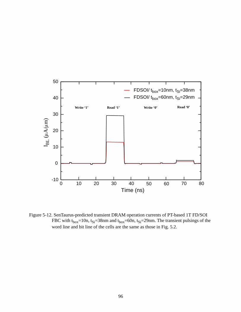
Figure 5-12. SenTaurus-predicted transient DRAM operation currents of PT-based 1T FD/SOI FBC with tbox=10n, tSi=38nm and tbox=60n, tSi=29nm. The transient pulsings of the word line and bit line of the cells are the same as those in Fig. 5.2.
0 10 20 30 40 50 60 70 80Time (ns)
I BL
(μA
/μm
)
-10
0
10
20
30
40
50
FDSOI/ tbox=10nm, tSi=38nmFDSOI/ tbox=60nm, tSi=29nm
Write ‘1’ Read ‘1’ Write ‘0’ Read ‘0’
96

CHAPTER 6SUMMARY AND FUTURE WORK
6-1 Summary
This dissertation is focused on physical analysis, modeling, and design of nanoscale DG
FinFET-based flash and floating-body DRAM cells. The major contributions of the research are
summarized as follows.
In Chapter 2, we developed, defined and verified a UFDG-based subcircuit model for the
paired-FinFET flash memory (VsNAND) cell, taking into account the fin-fin charge-coupling
effect. The model accurately predicted the sensitivities to process-induced parameter variations
and the fin-fin charge coupling. The subcircuit model was used to successfully simulate the
VsNAND-array (string) operations, predicting correct values of Best On-Cell Current, Worst On-
Cell Current, and Off-Cell Current. Finally, the model was easily extended to be applicable to the
floating-gate flash. This compact physics/process-based model is useful for checking and
analyzing the signal margins and process sensitivities for the VsNAND FLASH array, as well as
for aiding the paired-FinFET design.
In Chapter 3, we examined the memory-margin dependences on UTB thickness of
nanoscale planar thin-BOX FD/SOI and quasi-planar DG FinFET FBCs cells and attained
physical insights. We found that the thin-BOX FD/SOI FBC suffers from abrupt current-signal
margin degradation with UTB scaling because of loss of body accumulation charge, as well as
loss of inversion charge due to increased threshold voltage. Further, thin tSi, with the needed
accumulation, yields high transverse electric field, which leads to mobility degradation and
additional loss of margin. We also found that the DG FinFET FBC suffers from nominally low
signal margin due to a relatively low, 2-D effective body coefficient, as well as gradual margin
97

loss with fin-UTB scaling due to loss of accumulation charge at the base of the fin. Both 1T-
DRAM cells hence seem to have limited scalability.
In Chapter 4, we analyzed the basic operation of BJT-based 1T DRAM cells on SOI, and
derived physical insights. We found that the charging process (write ‘1’) is extremely sensitive to
the time offset (ΔtWB) between the word-line and bit-line voltage pulses. We noted and explained
that a positive ΔtWB is necessary for successful write ‘1’ because it establishes a high gate
capacitance, which is the predominant charge-storage element in the BJT-based cell. We noted
that the role the gate capacitance plays enables fully depleted bodies without independent biasing
for accumulation charge to be used. We noted a bulk-accumulation effect that may undermine the
BJT and cell operations for thin tSi, resulting in loss of current margin and ultimate write-‘1’
failure. Considering sensitivities to process parameters, we argued that PD/SOI is not viable for
scaling down, while a FD-body device, such as the FD/SOI MOSFET or FinFET, will be needed
in the future. We noted that the serious hot-carrier reliability issues, due to the high drain voltage
(VDS) required for BJT latch, limit the viability of BJT-based capacitorless DRAM.
In Chapter 5, we proposed a novel PT-based 2T DG-FinFET FBC for low-VDS operation,
and demonstrated and verified its memory operation via numerical simulations. We showed that
this FBC offers low-power operation, high sense margin, long worst-case retention times, and
good compatibility for embedded memory applications in future nanoscale CMOS technology.
We provided physical insights on the PT-based memory effect that depends on the modulation of
PT current by the stored-charge in the floating body via controlling φbarrier. We noted that the
enhanced DIBL associated with a thick body of the FinFET is critical for PT-based memory
operation. We designed a PT-based FBC with a 2T structure, which not only improves the worst-
case ‘0’ retention time under BL disturb but also greatly reduces the hold-‘1’ leakage current for a
viable memory array. We also verified the functionality of a PT-based planar thin-BOX FD/SOI
98

FBC. However, we found that, compared with the FinFET counterpart, FD/SOI FBC suffers from
lower sense margin due to its finite body capacitance, worse CMOS compatibility, and lower
GIDL-charging efficiency due to its planar structure.
6-2 Future Work
In Chapter 2, we developed and verified a UFDG-based subcircuit model for the paired-
FinFET flash memory cell, taking into account the fin-fin charge-coupling effect. This model is
useful in simulating the flash array read operation, and for predicting and analyzing the signal
margins and process sensitivities. However, this model is incapable of simulating the FLASH
write and erase operations. Thus we had to assume a certain amount of charges stored in the
nitride layer of the ONO stack to distinguish the programmed and erased transistors. This model
should be extended for simulating the complete flash memory operations, including the write and
erase operations.
In Chapter 5, we proposed a novel PT-based 2T DG-FinFET FBC for low-VDS operation.
We used numerical simulation to demonstrate the memory operation of this 2T FBC and predict
the memory performance. In the future, experimental demonstration of the DRAM operation of
the PT-based FBC should be done to further verify its viability. Although we have already
proposed a 2T cell structure to improve the retention time, optimization of process should also be
considerated for the actual FBC to minimize the junction recombination characteristics for longer
retention times. To guarantee good yield and memory performance, a thorough examination of the
sensitivities of the PT-based FinFET FBC to process-induced parameter variations should be
made. And, since the proposed PT-based FBC utilizes FinFET-on-SOI technology for future
embedded memory applications, the relevant circuit for the sense amplifier, and biases, should be
designed based on FinFET technology.
99

LIST OF REFERENCES
[1] International Technology Roadmap for Semiconductors, Semiconductor Industry Association, Austin, TX, 2007.
[2] K. Kim and G. Jeong., “Memory Technologies for Sub-40nm Node,” IEDM Tech. Dig., pp. 27-30, Dec. 2007.
[3] J. G. Fossum, L. Q. Wang, J-W. Yang, S.-H. Kim, and V. P. Trivedi, “Pragmatic Design of Nanoscale Multi-gate CMOS,” IEDM Tech. Dig., pp. 613-616, Dec. 2004.
[4] International Technology Roadmap for Semiconductors, Semiconductor Industry Association, Austin, TX, 2005.
[5] K. Kim, “Technology for Sub-50 nm DRAM and NAND Flash Manufacturing,” IEDM Tech. Dig., pp. 323-326, Dec. 2005.
[6] J.-M. Koo, et al., “Vertical Structure NAND Flash Array Integration with Paried Fin-FET Multi-bit Scheme for High-density NAND Flash Memory Application,” Proc. VLSI Symp.,pp. 120-121, June 2008.
[7] S. Lombardo, et al., “Advantages of the FinFET Architecture in SONOS and Nano-crystal Memory Devices,” IEDM Tech. Dig., pp. 921-924, Dec. 2007.
[8] P. Xuan, et al., “FinFET SONOS Flash Memory for Embedded Applications,” IEDM Tech. Dig., pp. 609-613, Dec. 2003.
[9] C. W. Oh, et al., “Damascene Gate FinFET SONOS Memory Implemented on Bulk Silicon Wafer,” IEDM Tech. Dig., pp. 893-896, Dec. 2004.
[10] S. Kim, et al., “Paired FinFET Charge Trap Flash Memory for Vertical High Density Storage,” Proc. VLSI Symp., pp. 104-106, June 2006.
[11] K. Kim and J. Choi, “Future Outlook of NAND Flash Technology for 40nm Node and Beyond,” IEEE NVSMW, pp. 9-11, 2006.
[12] L. Perniola, et al., “Physical Model for NAND Operation in SOI and Body-Tied Nanocrystal FinFLASH Memory,” IEDM Tech. Dig., pp. 943-946, Dec. 2007.
[13] H. Lee, et al., “Fully Integrated and Functioned 44nm DRAM Technology for 1GB DRAM,” Symp. VLSI Tech. Dig., pp. 86-87, June 2008.
[14]
Mat06a
J.Y. Kim, et al., “The Breakthrough in Data Retention Time of DRAM Using Recess-Channel-Array Transistor (RCAT) for 88nm Feature Size and Beyond,” Symp. VLSI Tech. Dig., pp. 11-12, June 2003.
[15] S.-W. Chung, et al, “Highly Scalable Saddle-Fin (S-Fin) Transistor for Sub-50nm DRAM Technology,” Symp. VLSI Tech. Dig., pp. 32-33, June 2008.
100

[16] S. Jeannot et. al., “Toward Next High Performance MIM Generation: up to 30fF/μm2 with 3D Architechture and High-k Materials,” IEDM Tech. Dig., pp. 997-1000, Dec. 2007.
[17] T.S. Boscke, et al., “Tetragonal Phase Stabilization by Doping as an Enabler of Ther-mally Stable HfO2 based MIM and MIS Capacitors for Sub-50nm Deep Trench DRAM,” IEDM Tech. Dig., pp. 1-4, Dec. 2006.
[18] H.-J. Wann and C. Hu, “A Capacitorless DRAM Cell on SOI Substrate,” IEDM Tech. Dig., pp. 635-638, Dec. 1993.
[19] S. Okhonin, M. Nagoga, J.M. Sallese, and P. Fazan, “A SOI Capacitor-less 1T-DRAM Concept,” Proc. IEEE Internat. SOI Conf., pp. 153-154, Oct. 2001.
[20] I. Ban, et al., “Floating Body Cell with Independently-controlled Double Gates for High Density Memory,” IEDM Tech. Dig., pp. 573-576, Dec. 2006.
[21] R. Ranica, et al., “A One Transistor Cell on Bulk Substrate (1T-Bulk) for Low Cost and High Density eDRAM,” Symp. VLSI Tech. Dig., pp. 128-129, June 2004.
[22] T. Shino, et al.,“Floating Body RAM Technology and its Scalability to 32nm Node and Beyond,” IEDM Tech. Dig., pp. 281-284, Dec. 2004.
[23]
Tri03
S. Okhonin, et al., “FinFET Based Zero-Capacitor DRAM (Z-RAM) Cell for Sub 45nm Memory Generations,” Proc. Internat. Conf. Memory Tech. and Design (IC-MTD)., pp. 63-65, May 2005.
[24] T. Shino, et al., “Floating Body RAM Technology and Its Scalability to 32nm Node and Beyond, ” IEDM Tech. Dig., pp. 569-572, Dec. 2006.
[25]
Tri05b
U.E. Avci, et al, “Floating Body Cell (FBC) Memory for 16-nm Technology with Low Variation on Thin Silicon and 10nm BOX,” Proc. IEEE Internat. SOI Conf., pp. 29-30, Oct. 2008..
[26] N.Collaert, et al., “Analysis of Sense Margin and Reliability of 1T DRAM Fabricated on Thin-film UTBOX Substrate,” Proc. IEEE Internat. SOI Conf., Oct. 2009
[27]
Lee05
I. Ban, et al., “A Scaled Floating Body Cell (FBC) Memory with High-K+Metal Gate on Thin-silicon and Thin-BOX for 16nm Technology Node and Beyond,” VLSI Symp. Tech. Dig., pp. 92-93, June 2008.
[28]
Kim06
M. Nagoga, et al., “Retention Characteristics of Zero-capacitor RAM (Z-RAM) Cell Based on FinFET and Tri-gate Devices,” Proc. IEEE Internat. SOI Conf., pp. 203-204, Oct. 2005.
[29] J. G. Fossum, Z. Lu and V. P. Trivedi, “New Insights on “Capacitorless” Floating-body DRAM cell,” IEEE Electron Device Lett., vol. 28, pp. 513-516, June 2007.
[30] S. Okhonin, et al.,, “New Generation of Z-RAM,” IEDM Tech. Dig., pp. 925-928, Dec. 2007.
101
[31] S. Okhonin, et al.,, “Ultra-scaled Z-RAM cel,” Proc. IEEE Internat. SOI Conf., pp. 157-158, Oct. 2008.
[32] K.-W. Song, et al., “55 nm Capacitor-less 1T DRAM Cell Transistor with Non-overlap Structure,” IEDM Tech. Dig., pp. 797-800, Dec. 2008.
[33] T.-S. Jang, et al., “Highly Scalable Z-RAM with Remarkably Long Data Retention for DRAM Application,” Proc. VLSI Symp., pp. 234-235, June 2009.
[34] A. Singh, et al, “A 2ns-read-latency 4Mb Embedded Floating-body Memory Macro in 45nm SOI Technology,” ISSCC Dig. Tech., pp. 460-462, Feb. 2009.
[35] Z. Zhou, J. G. Fossum and Z. Lu, “Physical Insights on BJT-Based 1T DRAM Cells,” IEEE Electron Device Lett, vol. 30, pp. 565-567, May 2009.
[36] K. Kim, “The Future Prospect of Semiconductor Nonvolatile Memory,” Symp. VLSI-TSA-Tech., pp. 88-94, Apr. 2005.
[37] J.-D. Lee, S.-H. Hur, and J.-D. Choi, “Effects of Floating-gate Interference on NAND Flash Memory Cell Operation,” IEEE Electron Device Lett, vol. 26, pp. 264-266, May 2002.
[38] Y. Shin, et al.,“A Novel NAND-type MONOS Memory using 63 nm Process Technology for Multi-gigabit Flash,” IEDM Tech. Dig., pp. 327-330, Dec. 2005.
[39]
Tau98
Y. Park, et al., “Highly Manufacturable 32 Gb Multi-level NAND Flash Mem-ory with 0.0098 μm2 Cell Size using TANOS (Si-Oxide-Al2O3-TaN) Cell Tech-nology,” IEDM Tech. Dig., pp. 11-13, Dec. 2006.
[40] T. Sugizaki, et al., “Novel Multi-bit SONOS Type Flash Memory Using a High- k Charge Trapping Laye,” Proc. VLSI Symp.,pp. 27-28, June 2003.
[41] S. K. Sung, et al.,“SONOS-type FinFET Device Using P+ Poly-Si Gate and High-K Blocking Dielectric Integrated on Cell Array and GSL/SSL for Multi-Gigabit NAND Memory,” Proc. VLSI Symp.,pp. 86-87, June 2008.
[42] J. R. Hwang, et al., “20 nm Gate Bulk-FinFET SONOS Flash,” IEDM Tech. Dig., pp. 154-157, Dec. 2005.
[43] M. Specht, et al., “20nm Tri-gate SONOS Memory Cells with Multi-level Opera-tion,” IEDM Tech. Dig., pp. 1083-1087, Dec. 2004.
[44] S.-H. Lee, et al., “Improved Post-cycling Characteristic of FinFET NAND Flash,” IEDM Tech. Dig., pp.33-36, Dec. 2006.
[45] J. G. Fossum, “UFDG MOSFET MODEL (Ver. 3.7) User’s Guide,” SOI Group, Univ. Florida, Gainesville, July 2007.
[46] Y. Taur and T. H. Ning, Fundamentals of Modern VLSI Devices. Cambridge, U.K.: Cambridge Univ. Press, 1998.
102

[47] V. P. Trivedi, J. G. Fossum, and W. Zhang, “Threshold Voltage and Bulk-inversion Effects in Nonclassical CMOS Devices with Undoped Ultra-thin Bodies,” Solid-State Electron., vol. 51, pp. 170-178, Jan. 2007.
[48] Z. Lu and J. G. Fossum, “Short-Channel Effects in Independent-Gate FinFETs,” IEEE Electron Device Lett., vol. 28, pp.145-147, Feb. 2007.
[49] J. W. Hyun, “NAND Array/String,” SAIT Document, Feb. 2007.
[50] I.S. Joe “VsNAND Array Structure,” SAIT Document, Jun. 2007.
[51] Taurus-2006 User’s Manual. Durham, NC: Synopsys, Inc., 2006.
[52] V. P. Trivedi and J. G. Fossum, “Scaling Fully Depleted SOI CMOS,” IEEE Trans. Electron Devices, vol. 50, pp. 2095-2103, Oct. 2003.
[53] J.-W. Yang and J. G. Fossum,. “On the Feasibility of Nanoscale Triple-gate CMOS Transistors,” IEEE Trans. Electron Devices, vol. 52, pp. 1159-1164, June 2005.
[54] S. Chouksey, J. G. Fossum, and S. Agrawal, “Insights on Design and Scalability of Thin-BOX FD/SOI CMOS,” IEEE Trans. Electron Devices, vol. 57, p. 2073-2078, Sep. 2010.
[55] K.-R. Choi, et al., “Dependence of Memory Margin of Cap-less Memory Cells on Top Si Thickness,” Appl. Phys. Lett., vol. 94, 023508 (online), 2009.
[56] H. K. Lim and J. G. Fossum, “Threshold Voltage of Thin-film Silicon-on-insulator (SOI) MOSFETs,” IEEE Trans. Electron Devices, vol. 30, pp. 1244-1251, Oct. 1983.
[57] K. I. Na, et al., “Gate-induced Floating-body Effect (GIFBE) in Fully Depleted Triple-gate n-MOSFETs,” Solid State Electron., vol. 53, pp 150-153, Feb. 2009.
[58] Z. Lu, et al., “A Novel Two-transistor Floating-body/gate Cell for Low-power Nano-scale Embedded DRAM,” IEEE Trans. Electron Devices, vol. 55, pp. 1511-1518, June 2008.
[59] Z. Lu, et al., “A Simplified, Superior Floating-body/gate DRAM Cell,” IEEE Electron Device Lett., vol. 30, pp. 282-284, Mar. 2009
[60] J. G. Fossum, et al., “Anomalous Subthreshold Current-Voltage Characteristics of n-Channel SOI MOSFET,” IEEE Electron Device Lett, vol. 8, pp. 544-546, Nov. 1987.
[61] J.-Y, Choi and J.G. Fossum, “Analysis and Control of Floating-Body Bipolar Effects in Fully Depleted Submicrometer SOI MOSFETs,” IEEE Trans. Electron Devices, vol. 38, pp. 1384-1391, June 1991.
[62] J. G. Fossum, “A Unified Process-Based Compact Model for Scaled PD/SOI and Bulk-Si MOSFETs,” Tech. Proc. Fifth Internat. Conf. on Modeling and Simulation of Microsystems (WCM), pp. 686-689, Apr. 2002.
103

[63] A. Aoulaiche, et al, “BJT Mode Endurance on a 1T-RAM Bulk FinFET Device”, IEEE Electron Device Lett. vol.31, pp. 1380-1382, Dec. 2010.
[64] R.J.T. Bunyan, M.J. Uren, N.J. Thomas and J.R. Davis, “Degradation in Thin-Film SOI MOSFET’s Caused by Single-Transistor Latch,” IEEE Electron Device Lett. vol. 11, pp. 359-361, Sept. 1990.
[65] Z. Zhou, J. G. Fossum, Z. Lu, "Physical Insights on the Memory Margin of Scaled (Fully Depleted) Floating-body 1T DRAM Cells," to be submitted to IEEE Trans. Electron Devices.
[66] M. Aoulaiche, et al., “Reliability Study in Capacitorless 1T-RAM Cells on SOI,” Proc. IEEE Internat. SOI Conf., pp. 157-158, Oct. 2010.
[67] Z. Lu, J. G. Fossum and Z. Zhou, "A Floating-body/gate DRAM cell Upgraded for Long Retention Time," to be submitted to IEEE Electron Device Lett.
[68] K.-Y. Fu and Y. L. Tsang, “On the Punchthrough Phenomenon in Submicron MOS Transistors,” IEEE Trans. Electron Devices, vol. 44, pp. 847-855, May 1997.
[69] B. M. Wilamowski and R. C. Jaeger, “The Lateral Punch-through Transistor,” IEEE Electron Device Lett., vol. 3, pp. 277-280, Oct. 1982.
[70] B. M. Wilamowski, “The Punch-through Transistor with MOS Controlled Gate, ” phys. stat.sol. (a), vol. 79, pp. 631-637, 1983.
[71] X. Li, et al., “Gate-controlled Punch Through Transistor,” University/Government/Idustry Microelectronics Symposium, pp. 226-229, Sep. 2003.
[72] K. E. Moselund et al., “Punch-through Impact Ionization MOSFET (PIMOS): From Devie Principle to applications, ” Solid-State Electronics, vol. 52, pp. 1336-1344, Sep. 2008.
[73] SenTaurus-2010 User’s Manual. Mountain View, CA: Synopsys, Inc., 2010.
[74] Y. Taur and T. H. Ning, Fundamentals of Modern VLSI Devices. Cambridge, U.K.: Cambridge Univ. Press, 2009.
[75] E. Yoshida and E. Tanaka, “A Capacitorless 1T-DRAM Technology Using Gate-induced Drain-leakage (GIDL) Current for Low-power and High-speed Embedded Memory,” IEEE Trans. Electron Devices, vol. 53, p. 692-697, Apr. 2006.
[76] R. K. Pandey et al, “Crystallographic-orientation-dependent Gate-induced Drain Leakage in Nanoscale MOSFETs,” IEEE Electron Device Lett., vol. 57, pp. 2098-2105, Sep. 2010.
104

BIOGRAPHICAL SKETCH
Zhenming Zhou was born in Huinan, China in 1981. He received the Bachelor of Science
and Master of Science in in optical and electrical information engineer from Zhejiang University,
Hangzhou, China in 2004 and 2006. He did his Doctor of Philosophy in electrical and computer
engineering at the University of Florida, Gainesville. His research interest concerns device theory,
modeling and design of non-classical silicon-on-insulator (SOI) and multi-gate MOSFET, for
both memory and logicapplications.
105