photonics in · pdf file2.2 focus areas for photonics in china ... in this report,...
TRANSCRIPT

1
Photonics in China
Opportunities for Dutch companies, institutes, and universities
December 13th , 2011
The copyright of this report is with NL Agency - Dutch Ministry of Economic Affairs, Agriculture, and
Innovation.

2
Contents
Executive summary ......................................................................................................................... 3
1. Introduction................................................................................................................................. 4
2. Organization of photonics in China ............................................................................................. 5
2.1 Research institutes and universities in photonics ..................................................................... 5
2.2 Focus areas for photonics in China............................................................................................ 9
2.3 Government funding and funding agencies (5 year plan)....................................................... 12
3. Report on fact finding mission in Shanghai, Wuhan, and Beijing ............................................. 13
3.1 Shanghai area – visited parties................................................................................................ 13
3.2 Shanghai area – additional institutes – not visited ................................................................. 16
3.3 Wuhan Area – visited parties .................................................................................................. 16
3.4 Wuhan area – additional institutes – not visited .................................................................... 19
3.5 Beijing Area – visited parties ................................................................................................... 20
3.6 Beijing area – additional institutes – not visited ..................................................................... 24
3.7 Shenzhen Area......................................................................................................................... 24
3.8 Changchun Area ...................................................................................................................... 25
4. Relevant events in 2012 (exhibitions, conferences, matchmaking).......................................... 26
5. References................................................................................................................................. 27
6. Fact-finding mission team ......................................................................................................... 30

3
Executive summary Photonics is recognized to be an important technology field that is growing rapidly on a global scale.
Also in China, photonic activities are growing fast. The number of people working in photonics in
China and the financial support by the government are huge. On the other hand, people are working
less efficiently according to western standards and collaboration between parties within China is still
limited.
Up till now the presence of Dutch photonic companies in the Chinese market has been limited to a
few players including Philips Lighting. Only a handful of Dutch SME’s have entered the Chinese
market. It turns out that knowledge of the Chinese market is limited for most SME’s.
In November 2011, a fact-finding mission on photonics in China was organized by NL Agency - the
executive agency of the Dutch Ministry of Economic Affairs, Agriculture, and Innovation in order to
get a proper feeling for opportunities for Dutch photonic companies and institutes entering the
Chines market. Universities, institutes and companies were visited in the cities of Shanghai, Wuhan,
and Beijing, all having extended photonic activities. Results of these discussions are reported in this
publication showing that there is ample opportunity for Dutch universities, institutes and companies
to start collaborating with Chinese counterparts.
Obviously only a small number of parties was visited during the fact-finding mission. Nevertheless, a
proper feeling for the Chinese photonics market has been created and useful contacts have been
established. These can be used for the matchmaking mission. There are definitely opportunities for
Dutch photonic companies in China.
Of course, cultural differences between the Dutch and Chinese can cause confusion or different
expectations. On the other hand, Chinese businesses are adapting to the demands of the global
market. This implies improved quality control and taking IPR more seriously.
The language barrier still is an issue: most Chinese don’t speak English, so an interpreter is often
required.
It is foreseen that a larger mission, taking place in 2012, will focus on matchmaking.

4
1. Introduction Photonics and photonic devices are becoming increasingly important both from a scientific and an
economic perspective. In fact it’s an enabling technology having impact in many sectors in terms of
photonic components, devices and technologies. The turnover of photonic technologies based
components was approximately Euro 43.5 billion in Europe in 2007. On a global scale, growth levels
between 10% and 40% are expected for this industry.
Extended photonics activities in the Netherlands, support by the government
In the Netherlands, we have a strong scientific position in photonics, and many companies are
involved in development, engineering, production, and M&S of photonic components and products.
Well-known players in this respect are e.g. ASML, Philips Lighting, and Thales, but many SME’s play
significant roles in niche markets as well.
The Dutch government (Ministry of Economic Affairs, Agriculture, and Innovation) acknowledges the
importance of photonics and supports activities in that field financially. A prominent example of this
is the research program IOP Photonic Devices. In this joint effort between universities and industry,
several innovative projects in the photonics area are being executed. Dr. Bart Verbeek is chairman of
this program and member of the fact-finding mission.
Chinese photonic companies becoming increasingly important
It’s obvious that the Asian market is growing rapidly, also for photonic-based products. Countries like
Japan and South Korea already have a strong position in photonics. China is catching-up quickly.
Having huge resources, both in finance and a well-trained dedicated workforce, it can be expected
that China will play a leading role in this field in the near future.
It should be noted that precise data on the size of the photonics market in China are hard to get as
most easy accessible literature is in Chinese. Numbers on the LED and Chinese laser market however,
could be retrieved and are shown in this report.
It is of vital importance for Dutch companies to be part of this emerging market as soon as possible:
on the one hand for sales opportunities for products developed and manufactured in the
Netherlands, but also for collaborating with Chinese companies, universities, and institutes. In joint
projects and joint ventures, new products can be developed together and the fast growing photonics
market in China offer opportunities for economic production. At the same time, China is a very
important market for new products.
Fact finding mission to prepare for a large mission in 2012
For entering the Chinese’ photonics market, the Dutch photonics sector is in need of information on
opportunities and challenges for collaboration. In that respect market figures, focus areas of Chinese
companies and institutes, do’s and don’ts are important too. Several Dutch companies have
indicated specific questions and needs.
It was concluded that a small fact finding mission could make the larger mission with companies in
2012 more effective. This fact finding mission took place in November 2011. Several universities,
institutes and companies were visited in Shanghai, Wuhan, and Beijing. In this report, conclusions

5
from these visits are presented together with results from literature search. Other regions of interest
will be discussed shortly.
Unfortunately, only a few systematic studies about China’s photonics industry are available. An
example of this is ref [1]. Most articles are in the Chinese language.
In this report, information and data on the photonics knowledge infrastructure and industry in China
will be presented with an emphasis on the cities of Shanghai, Beijing, and Wuhan.
2. Organization of photonics in China It goes without saying that China is a large country with huge resources in terms of man power and
money. At all places we visited, there was no lack of these resources. Nevertheless, advanced
equipment and components from western countries were in need, indicating that the Chinese
technology standard isn’t at the same level as ours in several fields. This, however, seems to be just a
matter of time. Photonics research and development has received a high priority from the
government resulting a massive financial support. It is thus foreseeable that the photonics field will
obtain the same level as in the western countries in a couple of years from now. At the same time,
China is a huge market for photonic products and Chinese companies and institutes are eager to
collaborate with counterparts from foreign countries in order to do joint R&D, production, and
marketing.
It should be noted that in China, the term ‘opto-electronics’ is often used instead of ‘photonics’.
2.1 Research institutes and universities in photonics
The laser and optoelectronic industry relies heavily on technological advancement as well as the
human resources that are available locally and nationwide. The academic and technology advantage
in a local area largely decides the future orientation or path of the industry there. By now, the
academically powerful cities with large achievements or potential in the laser and optoelectronic
technology and industry are Wuhan, Shanghai, Changchun, Beijing and Xi’an. An overview of major
academic institutes in this field is presented in Table 1.
Table 1 : Regional Major Academic and R& D establishments of laser and optoelectronics in China
Optoelectronic
Communication
Optoelectronic
Information (Storage,
Imaging)
Laser
Wuhan WRI HUST, WJI, Gongyan, 717
Shanghai CETC 23, SJTU, SEU
(Nanjing)
SITP SIOM,SILT
Changchun Jilin University CIOM, Jilin University CIOM
Beijing Beijing U. Tsinghua U. ISC, Nankai U.(Solar
Battery)
CETC11, BIOET, KLOP,
NCRIEO,BUT(NCLT),
Tsinghua
U., Beijing U.
Xi’an XOAI XIOM
Shijiazhuang CETC13

6
Guangzhou/Shenzhen OEMT of SYU GISM IOE of SCNU, GILA, SZU
Source: ref [1]; Official website of related institutions
Research institutes play and important role with respect to development of photonics in China. Many
of those research institutes are institutes of the Chinese Academy of Sciences (CAS). Historically CAS
institutes were the only organizations that were designated by the Chinese government to do
(applied) research as universities were focused on academic research and companies on production.
This clear division in tasks has become less strict, but the CAS headquarters still is a ministry-level
organization, including the financial privileges that come with that position.
Currently, quick profits can still be made in China by manufacturers just producing at a lower cost,
buying existing technologies instead of developing themselves. This situation is however changing,
especially in high-tech markets such as photonics, where quality and production speed rely on using
advanced manufacturing equipment. Because of the technological expertise and skills at the different
CAS institutes, they are often closely connected to the local Chinese industry.
Next to using CAS institutes to perform research, the Chinese government is also assigning State Key
Labs (SKL). When an existing Chinese laboratory or a professor has made good quality publications or
produced useful research results (and has good connections with the government), the laboratory
can obtain the status of a SKL. This means that they will have more/easier access to funding for
research. Table 2 gives an overview of State Key Labs having relevant activities in photonics.
Table 2: Distribution of SKLs for laser and optoelectronic technologies in China
Optoelectronic
devices
and materials
Optoelectronic
Information
Optoelectronic
Communication
Laser
Beijing
1) Superlattices
and
Microsturctures
2) Surface Physics
3)
Superconductivity
4) Magnetism
5) Artificial
Microstructures
and Mesoscopic
Physics
Software
Development
Environment
1) Networking
and
Switching
2) Microwave and
Digital
Communication
Shanghai Infrared Physics
1) Sensor
Technology
2) Optical
Communication
1) Optical and
Magnetic
Resonance
Spectroscopy
2) High Intensity
Optics
Wuhan
Software
Engineering
1) Spectroscopy,
Atomic
and Molecular
Physics
2) Laser
Technology

7
Changchun
Integrated
Optoelectronics
Applied Optics

8
Optoelectronic
devices
and materials
Optoelectronic
Information
Optoelectronic
Communication
Laser
Chengdu
Electronic Thin
Films
and Integrated
Devices
Microfabrication
Xi’an
Transient Optics
and
Photonics
Guangzhou
Optoelectronic
Materials
and Technology
Hangzhou Silicon Materials
Modern
Photonics
Apparatus
Jinan Crystal Materials
Nanjing
Solid State
Microstructures
Taiyuan Quantum Optics
Device
Tianjin Precision Test
Source: www. chinalab.gov.cn; ref. [1]
In China, 220 State Key Labs are present in various fields. The term State Key Lab qualifies for
additional financial support from the government. The SKL system is a measure of major China’s
basic research capacity. Altogether, there are 27 SKLs that are laser and optoelectronic, or photonic
related, accounting for 12.2%. And most of the 27 SKLs are located in the eastern part of China. Most
of the labs center on the basic science and a few of them act as technological providers, i.e. CIOM,
HUST and SIOM, to their affiliated spin-off companies and enterprises.
To get access as a student for a MSc or PhD position, a national exam has to be passed successfully.
Typically, a PhD-student earns 3000-5000 RMB (350-600 Euro) per month. Projects are partially
funded by companies. In that case, the company acquires the IPR. In order to get projects funded,
one has to submit proposals. Approximately 17% of the projects submitted to the National Science
Foundations are being granted. Obviously, not all key labs are on photonics: other State Key Labs are
working on topics like ship building, mechanical vibration, and thin film manufacturing for solar and
nanotechnology.
Such institutes and universities have powerful technological influence over the laser and
optoelectronic industries in China. For instance, almost all laser optoelectronic companies in
Changchun are spin-off enterprises of CIOM or technologically supported by CIOM.
The arrangement of such research institutes and universities is partly because of the central
government’s planning, like Changchun, and partly because of a city’s strategic position in China, like
Shanghai or Beijing. Due to their openness, all laboratories have various kinds of technological

9
coordination and academic communication with academicians from technologically advanced
universities and institutes. Although Beijing has the largest number of SKLs, it still lags far behind
Wuhan in the development of laser and optoelectronic industry. However, in some sectors that have
a technological disadvantage but large market potential industry, like LCDs and LEDs, the research
powers act as technological challengers to those multinational companies.
Apart from research establishments financed by the central government, there are also some
research institutes in technological agglomerated cities like Wuhan and Shanghai financed by local
government.
2.2 Focus areas for photonics in China
Four major regions witnessed the growth of the optoelectronic technology and industry. Next to
the three economically developed regions, i.e. the Yangtze River Delta, the Pearl River Delta and
the Bohai-bay Area, Wuhan and its surrounding cities have become the center of the laser and
optoelectronic industry.
Beijing, Shanghai, Wuhan, Nanjing, and Changchun are academic centers in laser and optoelectronic
technology in China. Wuhan tops the other cities in academic-engineering transfer, with a
strong research capacity agglomerated in it.
Due to the resource shortage in the eastern coastal areas and the guidance of the national policies,
China’s optoelectronics industry is seeing an accelerating relocation westward, forming the Central
Belt ranging from Chengdu in the west to Hefei in the east and the Eastern Belt ranging from Dalian
in the north to Zhuhai in the south.
Figure 1 Key Cities of China’s Optoelectronics Industry in 2010
http://event.ccidconsulting.com/en/images/en-map2.JPG. Source: CCID Consulting, May 2011
10
The European photonics21 report (ref. [3]) indicates that photonics production is dominated by Asia,
notably Japan, Korea, and Taiwan. But China is catching up, hosting production facilities of overseas
producers and Electronic Manufacturing Services (EMS). Also locally owned companies in China play
an increasing role.
According to the Chinese Photonics Industry Association, the photonics industry in China has gained
rapid growth in the past ten years with an average growth rate at about 20% each year. China has
achieved Outstanding photonics production in three out of ten sectors of photonics (ref. [3]):
Lighting (the LED segment): In the segment of LEDs, China is one of the fastest growing areas in the
world. It has built complete R&D capacity and industry chain, ranging from production of LED wafers,
chips, packaging to various LED applications for illumination, general lighting, display, signaling and
application products combining LED lighting with solar energy.
According to the Chinese Solid-State Lighting Alliance (CSA), more than 3000 Chinese companies are
engaged in LED industry in 2008, including about 25 ‘upper stream’ LED wafer and chips producers,
1000 doing packaging in the middle and 2000 ‘down stream‘ companies involved in LED application.
Every aspect of China LED industry, wafer, chips and packaging as well as application, has entered the
phase of economy of scale. China’s total LED production volume in 2008 is estimated at RMB 70
billion. This includes RMB 1.9 billion for chips production, which makes China the third biggest GaN
chips manufacturer. China has become an important manufacturing hub for world LED packaging, its
2008 production volume accounts for RMB 18.5 billion. The production of China’s LED applications
grew by 50% to RMB 45 billion in the same year.
China is not only a major manufacturer for LED products but also engine for growth and innovation in
R&D. China claims to have made major technological breakthroughs in deep UV LEDs and OLEDs. For
example: the Changchun Institute of Applied Chemistry at Chinese Academy of Sciences had
developed efficient tandem LED that can produce white light at a CRI rating of nearly 70, almost good
enough to read by.
In 2009, 6 ministries have presented proposals to develop the LED-lighting industry further. Until
2015, a yearly growth of 30% is expected. According to some branch experts, a production value of
500 billion RMB could be possible in 2015. Based on this figure, export of related products could raise
to $ 30 billion.
The driver for this, is the huge opportunity for reducing energy consumption. Already in 2009, 21
cities carried out pilots for using LED’s for lighting in public areas. Between 2010 and 2012 and other
50 demonstration projects are envisioned using approx.. 2 million LED-based lamps.
Optical communications: The Chinese industry holds a strong position in the sector of Optical
Communications, optical fiber and cable products as well as photoelectron devices. China Optical
fiber production is the second largest in the world, and accounts for more than a share of 12% of
total world production volume. In terms of R&D in photonic systems, China made major
technological breakthroughs in a 40Gb/s SDH (STM-256) Optic Communication Equipment and
System fiber-to-the-home (FTTH) project. This project aims at the highest line rate till date, viz.
40Gb/s, STM-256 SDH fiber-optic communication equipment and system. With the technologies
11
coming from Indigenous Innovation, the project team successfully developed the first STM-256
(40Gb/s) SDH equipment according to ITU-T standard in the world. This system transmits STM- 256
signal up to 560 KM on link or ring topology via widely used G.652 or G.655 fiber systems, and
provides the highest rated business system present till date by using expanding single-channel
bandwidth four times to 40Gb/s, compared to the predominant 10Gb/s single channel rate in
business systems.
Solar Energy: China is one of the major producers of solar panels and solar cells in the world.
However, this segment has not been subject of the fact finding mission. For more information on
Chinese activities in the solar energy market, see ref [1] and ref. [2].
Major activities in laser development and production
Chinese laser companies are mainly located in the provinces Hubei, Juilin, Jiangsu, and Guandong,
and near Beijing and Shanghai. According to the China Optics and Optoelectronics Manufacturers
Association (COEMA), approximately 200 companies cover 90% of the total laser market in China.
Companies like Wuhan Huagong Laser Engineering and Shenzhen have a position at the Shenzhen
stock market.
COEMA expects strong demand for high-power lasers for e.g. the steel industry. For the high
segment, German suppliers have a solid position in the Chinese laser market. Examples of such
German suppliers are Trumpf and Rofin-Sinar. Trumpf has a production facility in Taiceng for some
standard lasers.
China aims to reduce the dependency on import and several programs have been positioned to
increase technology build-up on high-power lasers. There are five national centers for laser research;
four of them are located in Wuhan. Nevertheless, it seems that up-till now, China isn’t able to
achieve the same quality as German competition.
The laser business is growing rapidly in China. Thanks to growing demand in many segments China
remains one of the most interesting markets for laser applications (ref [2]). China has been renowned
long for growing laser crystals and building Nd:YAG lasers. The segment for material processing
however is growing very fast (double digit numbers yearly) . Focus is on marking and engraving, but
also laser cutting in the lower and medium-power segments are growing significantly.
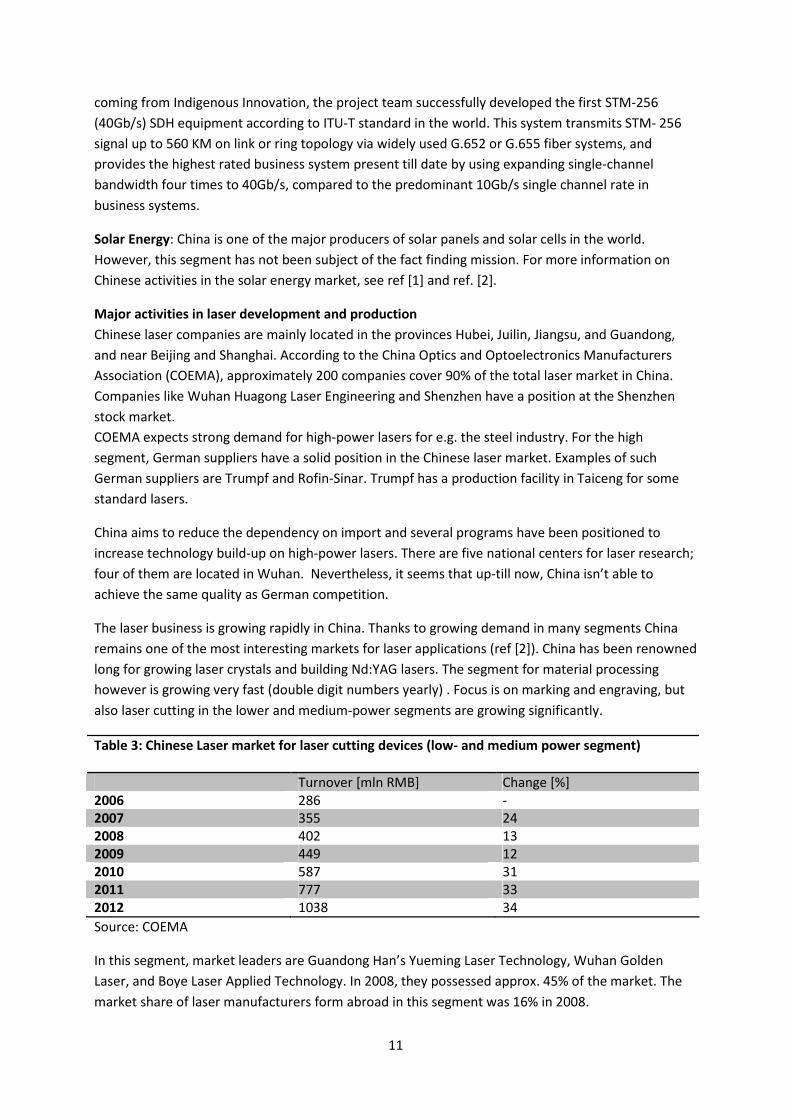
Table 3: Chinese Laser market for laser cutting devices (low- and medium power segment)
Turnover [mln RMB] Change [%]
2006 286 -
2007 355 24
2008 402 13
2009 449 12
2010 587 31
2011 777 33
2012 1038 34
Source: COEMA
In this segment, market leaders are Guandong Han’s Yueming Laser Technology, Wuhan Golden
Laser, and Boye Laser Applied Technology. In 2008, they possessed approx. 45% of the market. The
market share of laser manufacturers form abroad in this segment was 16% in 2008.

12
2.3 Government funding and funding agencies (5 year plan)
The National 12th Five-Year Plan on Science & Technology Development was released by the Ministry
of Science and Technology in July 2011. According to the Five-Year Plan, the overall objectives of
China’s science and technology development during the period of 2011-2015 will focus on ‘building
China into a knowledge based innovative nation by significantly boosting its strength for indigenous
innovation and its international competitiveness in high-tech sectors and achieving breakthroughs in
priority S&T areas and key technical fields.’
In its ‘Action Plan: Fostering strategic new industries’, one of the key areas is ‘Energy efficiency’
including LED lighting projects. This LED lighting part focuses on the development of key technologies
on white light emitting diode (LED), light source system integration and devices. The following goals
have been defined:
- Enhancing LED lighting applications
- Setting-up LED standards and testing system
- Speeding-up the "10 City, 10.000 LED lights" project
- By 2015:
� white LED luminous efficiency reaching international level
� LED accounts for 30% of the lighting in the Chinese market with expected turnover of 500
billion yuan
� China has to become top 3 in the world in LED lighting industry.
The 12th Development Plan for Information Technology also emphasizes other development areas of
photonics in China. These include:
· Optical communication network and system equipment
· Flat panel displays
· New optoelectronic devices, sensors and applications, terahertz sources
The objectives are to realize key technology breakthroughs through innovation, to build a complete
value chain, and to strengthen China’s overall competitiveness in the selected areas of photonics.

13
3. Report on fact finding mission in Shanghai, Wuhan, and Beijing As mentioned above, Shanghai, Wuhan, and Beijing are major cities for photonic activities that were
visited during the fact finding mission in November 2011. For each of these cities, results of the visits
will be presented below, together with additional information on related institutes and universities.
Next to this, information on institutes in the Shenzhen area are presented. This city has not been
visited during the fact finding mission.
3.1 Shanghai area – visited parties
In Shanghai, having a population of approx. 19 million, many universities, institutes, and companies
are engaged in photonic activities. It is interesting to note that in Shanghai, a free trade zone
(manufacturing for export) is present having financial benefits for both the Chinese government and
foreign companies.
The following parties were visited during the fact finding mission:
Shanghai Jiao Tong University
Jiao Tong University is present on five locations in China, including Taiwan. At the Shanghai site,
33.000 students are present together with 3000 faculty members.
This university houses six State Key Labs including the State Key Lab for Optical Communications
Research. It focuses on test beds, optical switching architectures and photonic devices. Every year
150 students graduate (MSc and PhD) and the faculty size is 40 persons. Several faculty members
have post-doc experience in Europe (including the Netherlands) or the US. For obtaining a degree,
publications in international journals are mandatory.
The SKL collaborates with 53 participants, including carriers, ( China Telecom), venders Huawei,
universities, and institutes. International collaboration has been realized with companies and
institutes from USA, UK, Germany, France, Singapore, and Korea. The collaborations have a bi-
directional character.
Research topics include:
1. Optical Networking - intelligent optical network design. In contrast to the choice made in
Europe, China has selected passive optical networks (PON) as the approach for ‘fiber to the
home’’. This choice has been made by the carrier.
2. Transmission & Switching
3. Opto-electronics & Photonics: working on theory of micro ring resonators and optical delay
lines for optical communication purposes.
The SKL are executing design activities for circuitry and in the process of setting-up their own
cleanroom. For this purpose, a budget of Euro 5 million is available. Up till now, they are using
foundry facilities in Singapore and Taiwan. Even then, not all facilities will be available. For example,
14
III-V facilities are not available and could be sourced from Cobra, Eindhoven, with whom they already
have contact.
Possible leads: collaboration on integration of electronics and photonics
Philips Lighting – Shanghai ( www.lighting.philips.com.cn )
The Philips LED-activities are concentrated in Shanghai. It is a competitive field with many active
competitors. During discussion with Philips employees, a couple of issues arose that could be of
interest for companies considering to start activities in China:
• There is a tendency for companies filing patents in China too, and trespassing is being
sanctioned . Nevertheless, IP has to be considered thoroughly in negotiations on
collaboration. The largest threat however are key employees transferring to the competitors
site. It is possible that a local company at the opposite side of the street, supported by the
government, starts competing with you, recruiting your best employees.
• For SME’s working with an agent is not always a solid way to go: if the loyalty of this person
ends, you’re facing transfer of your technology to a competitor. The best way to avoid this is
to take care that your product can’t be copied easily and to continue innovating.
NTS-Group- Shanghai ( www.nts-group.nl )
The NTS-group owns companies in the Netherlands, China, Czech, and Israel employing 800 people in
total of which 60 people at the Shanghai site. The central account management team is located in
Eindhoven. The company focuses on designing and manufacturing opto-mechatronic- and
mechanical modules for OEM companies. Application areas include healthcare, semiconductor,
analytical instrument, printing, and solar. This is a competitive field.
Starting as an after-sales center, NTS started series production in 2005, now also active in designing
for local customers. As the company’s activity is on assembling, most components are being sourced
locally from approx. 200 suppliers. Quality control is an issue taken care of. Also it is quite difficult to
find good designers.
Also the Frencken group is active in China having acquired a local company in the Shanghai area.
Shanghai Institute of Microsystem and Information Technology (SIMIT) http://english.sim.cas.cn/
This major institute is active in various fields of photonics and they are in the process of founding a
company on optics. They seem to have direct funding lines with central government as some of their
equipment/facilities are funded via the Mega Projects Zhongda zhuanxiang 国家科技重大专项
scheme. Current topics include:
• Silicon based photonics; Examples include a Ge-detector and a fiber-chip coupler. In the near
future the fiber-to-home market will be addressed. Next to this there is an interest in
biomedical applications. The institute has 30 years of experience in III-V materials and they
are searching for a foundry for research and volume production.
• A group is working on lasers and photo detectors, a.o. quantum cascade lasers in the
wavelength range of 4 – 10 micron. For wavelength tuning, an external cavity is used. A
single-photon emitter is being developed for quantum cryptography.

15
• 4 people are working on theory of photonic crystals. There is a close connection with MIT.
For the experimental part, another postdoc (from MIT) will start soon. The aim is to integrate
photonic crystals with III-V materials. Also thin-film techniques are being considered.
• Theory of plasmonics, no experiments yet
• THz-applications
Several employees have experience from institutes abroad (a.o. MIT, TU/e). Collaboration exists with
the French foundry LETI , IMEC / Holst Centre, and TUD (space applications for THz).
With respect to photonic crystals, the groups are oriented on MIT. There is no contact yet with
Dutch groups working on related topics.
With respect to experimental equipment, facilities are present for epitaxial growth. MOCVD is not
available yet.
Possible leads: the institute is interested in collaboration on microlenses for coupling light into chip
and on technologies for integrating electronics and photonics.
Shanghai Institute of Technical Physics (SITP) ( www.sitp.ac.cn )
This institute is large, having a staff of approx. 500 people and 400 temporary positions (graduate
students, post docs, and visiting professors). In 1998 it has been selected for knowledge innovation,
initiated by the Chinese Academy of Sciences (CAS).
Research includes fundamental issues (optical, electrical, and structural characterizations), materials
and devices (infrared detectors, coolers etc.), and systems and applications (a.o. remote sensors,
optical system design and electronics, and thin-film research).
Applications are mainly in the field of satellite technology for e.g. meteorology, and ocean
temperature monitoring. A high-spectral interferometer has been developed for methane detection.
SITP is working on studies only, on behalf of the Chinese Academy of Space Technology in Beijing. No
commercial activities. SITP helps companies in using the sensors.
Possible leads:
• Opportunities for collaboration on remote sensing applications
• The institute is searching for:
o gratings in the wavelength region 0.4 – 2.5 micron with 100 – 200 lines / mm
o detectors in the wavelength regions 3 – 5 micron and 8 – 12 micron
SCOP – Shanghai ( www.scop.com.cn )
SCOP is an example of a SME in the photonics area. Having six employees, the company has
developed burst trans-impedance- and post amplifier and laser driver for 2.5 Gb/s optical
communication. Application area is fiber-to-home.
They are in the process of pre-producing the chip using the IBM foundry. No sales have been realized
yet. SCOP is dedicated to the design on which they have filed patents.
16
3.2 Shanghai area – additional institutes – not visited
Shanghai Institute of Optics and Fine Mechanics (SIOM), CAS
• Website: http://english.siom.cas.cn/ (English)
• Keywords / focus area: High Power Laser Technique, Strong-Field Physics and High Intensity
Optics, Information Optics, Quantum Optics, Laser & Optoelectronic devices, and Optical
Materials, etc.
• Director: Zhu Jianqiang
Shanghai Jiao Tong University, Laboratory for Laser Plasmas
• Website: http://llp.sjtu.edu.cn/
• Keywords / focus area: lasers
3.3 Wuhan Area – visited parties
China’s biggest photoelectron information industry base, known as Optical Valley, is located in the
city of Wuhan, central China’s Hubei Province.
There are 18 universities and institutes, 56 state level research organizations and over 150,000 high-
technology experts in the area. About one third of the experts work in the photoelectron information
industry.
In May 2001, the Optical Valley Technology Stock Exchange was established in Wuhan. It was the first
optical technology exchange center in China. After less than one month’s operation, more than 200
projects were released and around 30 members had joined. The government has defined a 5-year
plan for activities on laser technology.
Also venture capital is available for this purpose: yearly, an exhibition is organized for Chinese and
foreign venture capital companies, and high-tech enterprises.
In Wuhan more than 200 photonic companies are active. Approximately 100 companies are
connected to the Center for Laser Processing. International collaboration exists with Russia, India
(major market for export), and Germany (Munich exhibition and contacts with major companies as
Siemens and Mercedes).
Other Optical Valleys are planned in south China’s Guangdong Province with the cooperation of the
US company Lucent Technology and Changchun, the capital of northeast China's Jilin Province, and
Shanghai Pudong New Area have plans for the construction of an Optical Valley and photoelectron
industry park of their own.
The following parties were visited during the fact finding mission:

17
Wuhan National Engineering Center for Laser Processing ( http://laser.hust.edu.cn )
The Wuhan National Engineering Center for Laser Processing aims for collaboration with SME’s. In
their opinion, large companies like Rofin-Sinar and Trumpf don’t need support.

18
The Engineering Center has 2 areas of interest:
1. High-power photonics
2. Information photonics
Ad 1: CO2-slab lasers have been acquired from Rofin-Sinar ; the high-power lasers are not allowed to
be built outside Germany. Also high-power fiber lasers are bought abroad. Application areas include
welding, cutting, and marking.
The Center is planning to build a high-power UV-laser. The route for this is to start with a750 W Q-
switched disk laser (Trumpf) and use non-linear optics for frequency doubling and mixing.
Chutian Laser Group ( www.chutianlaser.com )
Chutian Laser is a large company, having 1000 employees, in the field of laser applications. Also
welding, cutting, and marking activities are executed for customers.
Using commercially available lasers, Chutian develops laser systems for medical applications (e.g.
dermatology). In this respect Philips is a competitor.
Chutian is also marketing laser systems form other companies.
Possible leads: Chutian is interested in marketing Dutch products for the Chinese market, e.g. laser
systems or medical diagnostic tools. Next to this, they would like to collaborate on femtosecond laser
processing.
HG Laser ( www.hglaser.com )
The company is a spin-off activity from the university in Wuhan. The turnover in 2010 was 2.1 billion
RMB of which 50% is laser business. Other activities include counter fare, EO optical components,
and sensing parts using ceramics (PTC and NTC).
HG laser manufactures approximately 70-80 laser products: CO2-lasers, Nd:YAG (1064 nm, 532 nm,
355 nm) , fiber lasers, and diode-laser pumped lasers. Diodes are obtained from e.g. Coherent.
In the factory, they also had high-power Rofin-Sinar and IPG-lasers. They expect being able to build
such lasers themselves within two years from now.
The lasers manufactured are applied in e.g. welding, marking, and laser dicer machines.
A collaboration exists with Australian manufacturer Farley in the field of high-power CO2-laser
systems . A manager from this company will obtain a position in HG soon, a.o. to tackle quality issues.
Chutian is not considered a competitor as it is not building lasers itself, but using them for medical
applications. Chutian is privately owned whereas HG laser is state owned.

19
3.4 Wuhan area – additional institutes – not visited
For Wuhan, the focus of the visit was on laser industry. Wuhan is also a strong base regarding optical
fiber/cable, main players are
• Nat’l Engineering Lab for Fiber Optic Sensing Technology (linked to the Wuhan University of
Technology, visited by Teijing in March 2011) http://public.whut.edu.cn/fostrc
• Fiberhome Group: before a state-owned institute (WII), now being privatized. More information
can be found on www.fiberhomegroup.com. Production as well as R&D
• YOFC, joint venture with Draka. www.yofc.com.cn. Production as well as R&D. YOFC is said to
be one of the top-3 players in the world
Other major institutes in Wuhan:
Wuhan National Laboratory for Optoelectronics (WNLO)
• Website:
o http://222.20.94.9:8083/ (English)
o http://wnlo.cn/ (Chinese)
• Keywords / focus area: Fundamental Photonics, Integrated Optoelectronics and Micro-nano
Fabrication, Laser Science and Technology, Optical Network and Communication, Opto-
electro Measurement and Instrument, Optoelectrical Information Storage, Biomedical
Photonics and Optoelectronic Medical Devices, Organic Optoelectronics, Advanced
Optoelectronic Materials and Energy Optoelectronics
State Key Laboratory of Digital Manufacturing Equipment and Technology (DMET)
• Website: http://dmet.hust.edu.cn
• Keywords / focus area: Fundamental theory of digital manufacturing, Advanced process &
methods, Key technology of digital manufacturing equipment, Digital manufacturing systems
Huazhong University of Science & Technology (HUST), College of Optoelectronic Science and
Engineering
• Website: http://oe.hust.edu.cn:8082/Overview/Profile/index.html
• Keywords / focus area: optical fiber communication technology and sensing, high-power
laser, laser processing device and technique, MOSEMS technology, laser medical equipment,
optical storage technology, optical information detection and image processing technology
and military optical technology.
Huazhong University of Science and Technology (HUST), School of Life Science and Technology
• Website: http://english.hust.edu.cn/170_overview.html
• Keywords / focus area: Key Laboratory of Biomedical Photonics, Key Laboratory of Image
Processing and Intelligence Control.

20
3.5 Beijing Area – visited parties
Like Shanghai, Beijing is one of the major cities in China with over 19 million inhabitants. Numerous
universities, institutes and companies are working on photonics. Below, an overview is shown of the
visits paid during the fact finding mission.
CAS Institute of Semiconductors – Beijing (www.semi.ac.cn )
In this institute, both photonic components (LED and blue diode lasers) and applications are
developed.
With respect to components development, the total chain is explored and the focus is on increasing
efficiency of the devices. For research also a nano-optoelectronics lab is available.
LED-development is concentrated in the Beijing area, industrial applications in Xian Xu, and
manufacturing in the Guandong area.
The following applications are under development:
a. Plant growth (adapting the wavelengths to optimize growth)
b. Smart lighting (i.e. combining lighting and communication – internet access). This
could result in using internet in an airplane
c. Intelligent lighting – opening curtains, controlling air-conditioning using light
d. The blue LED is being considered / used for military communication, killing of
bacteria, and printing.
The UV-LED (< 200 nm) still has a low output power (order of 1 mW). It is the aim to increase the
output power to say 10 mW as it will be interesting for water treatment then. To realize this increase
of current and increasing the number of devices per unit are possible solutions. The institute is also
considering using Al-nitride for the blue-LED, but the lifetime is disappointingly low.
The institute have developed a platform for LED-production (including MOCVD-equipment).
Companies can get access to this platform.
Next to this, a group is working on III-V materials for military applications. Another group is working
on high-power all-solid-state lasers. With respect to the latter, there is no collaboration with
companies or institutes in the Wuhan-area.
TU Delft has realized a collaboration with this institute.
Possible leads: the institute would like to collaborate on
• Technologies for increasing LED efficiency (e.g. plasmonics)
• Technologies for generating light out of silicon
• Application areas such as water treatment and plant growth
ISA – Beijing ( www.isa-world.org )
ISA stands for International Solid-State Laser Alliance and is an association between the government
and companies working on roadmaps, standardization, and promotional issues of solid-state lighting.

21
LED development is a high priority for the Chinese government: it is part of out of seven strategic
emerging technology directions:
1. Energy savings; LED is part of this
2. New IT
3. Biotech
4. Automotive
5. New energy
6. New materials (including photonic materials)
7. Medical and well-being
There is a strong SME presence on LED in China with 4000 (!) enterprises active, divided over
luminaires, packaging, and chip manufacturing. With respect to the latter, 65 (!) GaAs foundries are
active in China.
Approximately 10 – 20 companies can be considered as leading in their field. While R&D is focused in
Beijing, most companies are located in het Shanghai and Guandong area.
In the Board of Advisors, Prof. Guoqi Zhang is co-chairman. He is also director at DIMES Centre for
SSL Technologies and professor at Delft University.
Philips Lighting and TNO are ISA members too. TNO has been contributing to the Strategic Research
Agenda (SRA) for this field. In the near future, the SRA will be converted into a roadmap.
Two times per year, an international forum and exhibition on LED is being organized. This event can
be used for matchmaking. In April 2012 the event will take place in Shanghai, in autumn 2012 in
Guandong.
China Academy of Space Technology – Beijing (http://www.cast.cn/CastEN/index.asp )
CASC (China Aerospace Science and technology Corporation, 20.000 employees, 22 billion RMB
turnover in 2011) is prime contractor for China national space crafts. The China Academy of Space
Technology is part of this institute.
Core businesses are space technology R&D and spacecraft design and manufacturing.
Technological development are:
1. Sensors for sun and stars research
2. Camera’s
3. Laser communication between satellites and from satellites to earth
With respect to the Netherlands, the China Academy of Space Technology has contacts with TU Delft,
SRON, and TNO. China Academy of Space Technology and TNO are collaborating on calibration of
instruments.
The institute is in need for CMOS-camera’s and a space-qualified laser instrument (optical amplifier).
Part of the program is military oriented. At the moment it is not clear if export limitations are an
issue.

22
Chinese Optical Society (http://english.cast.org.cn/ currently only in Chinese )
The Chinese Optical Society which is close to its US-counterpart OSA has a good overview of photonic
activities in China. It’s also working closely together with SPIE.
It is a non-profit organization, connected to CAST.
The China Academy of Sciences (CAS) has seven institutes that are specialized in photonics. An
institute in Chan Chun (north of China) has over 4000 staff members. The smallest institute has over
1000 staff members. In 25 out of 32 provinces of China, COS has sub-offices.
In China, there are approx. 17 institutes for PhD students, 100 institutes for MSc students, over 200
institutes for bachelor students. Yearly, 10.000 bachelor students graduate, together with 6.000 MSc
students and 1.000 PhD students.
As an example, at the Beijing institute for Optical Engineering, 150 bachelor students graduate each
year, together with 30 PhD’s. PhD positions are obtained by passing national exams.
The COS has several sub-societies and special committees in different fields, e.g. laser infrared
technology, optical engineering, holography, etc. This is a similar set-up as SPIE and OSA.
Focus areas for photonics in China are: semiconductors (lasers and components for telecom and
LED), lasers, and solar (photonics for energy)
COS has approx. 4.000 individual members.
COS organizes bi-annual conferences, the next taking place in October 2012 (ASIA Photonics). Sub-
committees also organize conferences.
The COS income has the following distribution:
• 10% membership fee
• 20-30% government support
• 50-60% technical support & services (exhibitions, training)
COEMA ( www.coema.org.cn )
China Optics and Optoelectronics Manufactures Association (COEMA) fills the gap between
government and companies. Activities include gathering and fact finding. They are also involved in
roadmaps for the five-year plan of the government and giving input to the strategic research agenda.
Formally, they are part of the MIIT ministry.
In China approximately 10.000 companies are active in the field of opto-electronics of which 800
have a membership of COEMA. This percentage is relatively small due to the large number of
associations that companies can subscribe to. Most of these companies produce components and
parts.
COEMA has several contacts abroad, e.g. with Canada, Japan, and Korea. In 2009 COEMA organized
an event in Beijing together with Germany. There is a collaboration with the German Association for
Medical Devices. In the past (2009) also matchmaking was organized with French companies.
COEMA and COS mostly cover similar fields, but COS is more scientific oriented and COEMA is more
enterprise oriented.

23
With respect to quality control, MIIT sent a survey last year to companies. The response was
however quite low; companies are reluctant sharing information on this topic.
Phoebus Vision ( www.phoev.com )
Phoebus Vision focuses on display technologies. It is a company co-funded by CAS and has 4
international patents.
Phoebus have developed a 71 inch HD TV using 3 lasers: a 638 nm diode laser, a frequency-doubled
diode laser pumped Nd:YAG laser and a blue laser by sum-frequency mixing the former two lasers.
Phoebus is claiming a lifetime of the lasers of 20.000 hours.
With respect to technology demands, Phoebus is searching for green and blue diode lasers and
integration of the display system (optical engine).
Looking at activities in the Netherlands, there may be a possibility for collaboration with parties
working on integrating electronics and photonics.
Beijing GK Laser Technology ( www.gklaser.com )
The main business of this company is manufacturing laser-diode pumped solid-state lasers. They are
part of the CAS Institute of Optics and Electronics. The company employs a staff of over 100 people
and have a ISO 9001 quality management system.
Part of the product development is what they call “self-directed innovation”, i.e. having free choice
for developing new products.
Several laser systems were presented:
• Several solid-state lasers (diode-laser pumped) in the range from 40 – 4000 W
• 100 W laser @ 532 nm
• Pico-second laser
• Fiber laser: 2 kW @ 1064 nm
• Amplifier @ 1053 nm (Nd: Glass ?, amplification 109 x?, pulse length 1-10 ns ?) for a secret
application (‘nuclear’)
Application areas for the lasers include laser shows, ceramics manufacturing, diamond cutting, silicon
scriber, marking.
GK Laser has international collaboration with Russia, Lithuania, Germany (Edgewave), US (Laser
Spectrum Corp., Yuco). No collaboration with similar companies and institutes in the Wuhan-area.
The turnover in 2010 was approximately 50 million RMB.
Laser diodes for their products are obtained from e.g. France and the US. They don’t make them
themselves.

24
3.6 Beijing area – additional institutes – not visited
Peking University – SPM Group
The Silicon, Photonics & Microsystems (SPM) Group is a platform for research and education on new
frontiers of nanophotonics and nanoelectronics. The objective is to develop the next generation of
compactly integrated low cost optoelectronic systems that may be used for real time
sensing/detection, high-density data communications, and high-speed control/actuation.
Website: http://spm.pku.edu.cn/
3.7 Shenzhen Area
During the fact-finding mission, the Shenzhen area has not been visited. Nevertheless, extended
photonic activities take place there. Below, an overview is given of relevant universities institutes in
that area.
Shenzhen Institutes of Advanced Technology (SIAT), Chinese Academy of Sciences
Comprehensive research institute(s) under SIAT characterized by an extremely wide coverage of
research areas and focus on industrial research in cooperation with (local) industry. Two photonics-
related departments (lab & research center; see website)
• Website:
o http://english.siat.cas.cn/ (English)
o http://english.siat.cas.cn/rh/rd/ioait/rcl/lfpit/in/ (Laboratory for Photonics Integrated
Technologies)
o http://english.siat.cas.cn/rh/rd/iobe/rcl_1/rcfb1/in/ (Research Center for Bio-
Photonics)
• Keywords / focus area: Bio-photonics, mixed-signal integrated circuits, high-density system-
on-package, miniaturization and multi-function integrated systems.
• Remarks: collaboration with Huawei on optical interconnected sender and receiver IC
Research Institute of Tsinghua University in Shenzhen (RITS)
Relevant research centers are the Center for Optomechatronics & Advanced Manufacturing, Center
for Advanced Materials & Biotechnology.
• Website:
o http://en.tsinghua-sz.org/ (English)
o http://en.tsinghua-sz.org/Research.aspx?CateID=356 (Center for Optomechatronics
& Advanced Manufacturing)
o http://en.tsinghua-sz.org/Research.aspx?CateID=264 (Center for Advanced Materials
& Biotechnology)
• Keywords / focus area: optomechatronics integration, micro-nano engineering, micro electro
mechanical systems, sensor technology.

25
Shenzhen University Institute of Optoelectronics
Besides the Institute of Optoelectronics Engineering (see website), Shenzhen University houses two
Shenzhen key labs: Key Lab of Laser Engineering, Key Lab of Micro-Nano Photonic Information
Technology.
• Website:
o http://opto.szu.edu.cn/en/General_info.htm (English; outdated)
o http://opto.szu.edu.cn/cn/ (Chinese; College of Optoelectronics Engineering;
updated)
• Keywords / focus area: ultra-fast diagnostic technology, flat display technology,
semiconductor material & devices, electro-optics systems, vacuum ultra-fast photoelectric
devices, laser technology.
• Remarks: Shenzhen University’s reputation is not particularly strong
As an example of the importance of the Shenzhen area: the company Huawei (www.huawei.com), a
leading company on global information and communications technology are executing their
photonics R&D in Shenzhen.
3.8 Changchun Area
The Changchun area hasn’t been visited during the fact-finding mission. Also here, several photonic
activities take place that are worth mentioning:
Changchun Institute of Optics, Fine Mechanics and Physics (CIOMP), CAS
CIOMP belongs to the Chinese Academy of Sciences (CAS). It is a multi-disciplinary and
comprehensive research institute. It is engaged in fundamental research, applied fundamental
research, engineering technology research and high-tech industrialization.
Main topics of research: luminescence, applied optics, optical engineering, precision mechanics and
Instruments.
CIOMP has 13 research departments, laboratories and centers, including the State Key
Laboratory of Applied Optics, National Engineering Research Center for Diffraction Gratings
Manufacturing and Application, the National Supervision and Test Center for Optics Mechanics
Quality and the Key Laboratory of Excited State Processes, CAS.
Website: http://english.ciomp.cas.cn/
Jilin Photonics Industry Incubator
Jilin Provincial Photonics Industry Incubator is financially supported by the Jinlin provincial
government. More than 60 companies are based in this incubator.
Products include: optical measurement and control products, light-emitting materials, information
display, optical element base parts, semiconductor packaging equipment, laser imaging devices, laser
processing equipment, medical devices for clinical testing etc.

26
4. Relevant events in 2012 (exhibitions, conferences, matchmaking) In case the company mission to China will be combined with a conference or trade show, the
following events could be considered in 2012:
Date (2012) City Conference / tradeshow Info
February 22-
24
Shanghai China (Shanghai) International
Optics Fair
http://www.siof.cn
March 20-22 Shanghai Laser World of Photonics China http://www.world-of-
photonics.net/en/laser-china/start
April 26-29 Xiamen International Symposium on
Advanced Optical manufacturing
and Testing Technologies
(AOMATT)
http://www.ioe.ac.cn/gjjl/jldt/20111
1/P020111103360981754881.pdf
May 21 – 23 Shanghai SOPO 2012 — International
Symposium on Photonics and
Optoelectronics
www.sopoconf.org/2012
June 12-14 Beijing China International
Photoelectronic Exhibition
www.cipeasia.com
July 18-20 Shanghai The 11th China (Shanghai)
International Optoelectronics
Expo
http://www.chinaexhibition.com/tra
de_events/1080-
Optoelectronics_Shanghai_2012_-
_The_11th_China_%28Shanghai%29
_International_Optoelectronics_Exp
o.html
September
6-9
Shenzhen The 14th China International
Optoelectronic Expo
http://www.cioe.cn/files/CIOE%202
012%20Invitation%20Brochure.pdf
September
10-12
Beijing CIOF 2012 - The 25th China
(Beijing) International Optics Fair
www. coif.cn/eng/fairinfo.php?p=4
November
2-9
Wuhan 9th Optics Valley of China Int’l
Optoelectronic Exposition and
Forum (OVC Expo 2012)

27
5. References
1. ‘A Study on the Development of China’s Laser & Optoelectronic Technology and Industry’, with
city cases of Wuhan, Shanghai and Changchun, Hao Wang, University of Giessen, 2008,
http://fss.plone.uni-
giessen.de/fss/fbz/fb07/fachgebiete/geographie/forschung/pdf/wirtschaft3/file/2008-
03_Studi_z_WiGeo_Development%20of%20China.pdf
2. Der Photonikmarkt in der VR China, Germany Trade & Invest, www.gtai.de , 2010
3. Photonics in Europe, Photonics21, 2007
4. Zakendoen en kansen in China voor de fotonica sector, NL Agency, January 2010
Additional information from internet:
<<<<Acta Photonica Sinica>>>>
‘ACTA PHOTONICA SINICA is a monthly journal which is sponsored and edited by The Chinese Optical
Society, co-sponsored by Xi'an Institute of Optics and Precision Mechanics, CAS, and published by
Science Press. It mainly publishes academic theses, research notes and research letters on Photonics.
The contents deal with Optics, particularly, Transient Optics, Optoelectronics, Integrated Optics,
Optics, Nonlinear Optics, Photo-Biology, Optical Information Optics, Guided Wave Communication,
Optical Sensing, Optical Computing, Optical Neural Network, High Speed Photography,
Intellectualized Optical Instrument, Photon Function Materials, Interaction between Photons,
Classical and Nonclassical effects of Photons, etc. ‘
Website: www.photon.ac.cn
Email: [email protected]
Add: P.O. Box 47, 17 Xinxi Road, New Industrial Park, Chang'an District, Xi'an, Shaanxi, P.R. China
Post code: 710119
<<<<China Laser Press>>>>
‘A new magazine of Chinese Laser Press, is featured by OE news, products and market reports, and

28
the circulation covers OE-related companies, universities and institutes. It aims to accelerate China
OE research and industrial development. The main columns include news, viewpoint, interview,
focus, technology exchange, product information, etc.
OEPN provides readers a channel to know the OE market and buy devices, and it is also a favorable
platform of promoting products for companies.’
<<<<Lightwave China>>>>
‘Launched in September, 2002, Lightwave China Bimonthly is the Chinese version of the well-known
Lightwave magazine. Lightwave China is authorized to publish by Pennwell and is published in
Simplified Chinese by ACT International in Hong Kong, circulating controlled-free to average of
10,000 professionals in the China optical communications industry.
Focusing on optical communication, Lightwave China provides engineers and senior executives in
China with in-depth information about optical communication technologies, up-to-date news,
applications, market, products and standards, etc.
Lightwave China magazine organizes “FTTH China Conference” annually, and manages
www.lwc.com.cn, a professional website for optical communication.’
<<<<Laser Focus World China>>>>
‘The Premier Publication for Laser and Opto-Electronics Industry in China Published since 2005, Laser
Focus World China, the Chinese edition of the well-known Laser Focus World magazine, is the
professional magazine for engineers, researchers, scientists, and technical professionals in China. It
provides comprehensive global coverage of optoelectronic technologies, industrial and R&D
applications, and market information. The editorial content licensed exclusively from LFW is
supplement by content generated by our own editors in China. Laser Focus World China is published
every other month in simplified Chinese and distributed to over 8,000 qualified optoelectronics
professionals in China. Through our digital magazine and website we provide coverage to an even
larger audience base.’
<<<<International Optoelectronics and Displays>>>>
‘Founded in 1999 by Yawei Information Co., Ltd., “International Optoelectronics and Displays” is the
most popular FPD Industry magazine in China, and it is the only industry magazine recognized by
China Optics & Optoelectronics Industry Manufactures Association LCD Branch and Shenzhen Flat

29
Panel Display Industry Association. It introduces the latest industry development trends or
companies' demand information to readers.’

30
6. Fact-finding mission team
This fact-finding mission was conducted by:
Jan Willem Gerritsen – PhotonTec BV
Bart Verbeek – Barnel BV, IOP Photonic Devices
Nasrat Popal – NL Agency
We gratefully acknowledge the support and input of the staff of the Royal Embassy of The
Netherlands in China (including the Science and Technology Office in Beijing and Shanghai) and
Netherlands Business Support Office (NBSO) in Wuhan.
Dutch Embassy, Beijing:
Jan Reint Smit
Harro Wintermans
Jingmin Kan
Maurits van Dijk
Ma Qing
Dutch Consulate, Shanghai:
Jaap van Etten
Netherlands Business Support Office Wuhan:
Bertrille Snoeijer
Yuan Fei