photolithography: alignment and exposurepoe.nctu.edu.tw/upload/...smt-14~1photolithography.pdf ·...
TRANSCRIPT

Yau - 1SMT
Photolithography: Alignment and Exposure
Photolithography: Alignment and Exposure

Yau - 2SMT
ObjectivesAfter studying the material in this chapter, you will be able to:
1. Explain the purpose of alignment and exposure in photolithography.
2. Describe the properties of light and exposure sources important for optical lithography.
3. State and explain the critical aspects of optics for optical lithography.
4. Explain resolution, describe its critical parameters, and discuss how it is calculated.
5. Discuss each of the five equipment eras for alignment and exposure.
6. Describe reticles, explain how they are manufactured and discuss their use in microlithography.
7. Discuss the optical enhancement techniques for sub-wavelength lithography.
8. Explain how alignment is achieved in lithography.

Yau - 3SMT
Eight Basic Steps of Photolithography
Step ChapterCovered
1. Vapor prime 132. Spin coat 133. Soft bake 134. Alignment and exposure 145. Post-exposure bake 156. Develop 157. Hard bake 158. Develop inspect 15
Table 14.1

Yau - 4SMT
Three Functions of the Wafer Stepper
1. Focus and align the quartz plate reticle(that has the patterns) to the wafer surface.
2. Reproduce a high-resolution reticle image on the wafer through exposure ofphotoresist.
3. Produce an adequate quantity of acceptable wafers per unit time to meet production requirements.

Yau - 5SMT
Reticle Pattern Transfer to Resist
Single field exposure, includes: focus, align, expose, step, and repeat process
UV light source
Reticle (may contain one or more die in the reticle field)
Shutter
Wafer stage controls position of wafer in X, Y, Z, θ)
Projection lens (reduces the size of reticle field for presentation to the wafer surface)
Shutter is closed during focus and alignment and removed during wafer exposure
Alignment laser
Figure 14.1

Yau - 6SMT
Layout and Dimensions of Reticle Patterns
4) Poly gate etch1) STI etch 2) P-well implant 3) N-well implant
8) Metal etch5) N+ S/D implant 6) P+ S/D implant 7) Oxide contact etch
Top view
1
23
45
7
6
8 Cross section
Resulting layers
Figure 14.2

Yau - 7SMT
Optical Lithography
Light• Interference of Light Waves
– Optical Filters
• Electromagnetic Spectrum

Yau - 8SMT
Light Wavelength and Frequency
λ
λ = vf
Laser
v = velocity of light, 3 ’ 108 m/secf = frequency in Hertz (cycles per second)λ = wavelength, the physical length of one
cycle of a frequency, expressed in meters
Figure 14.3
Yau - 9SMT
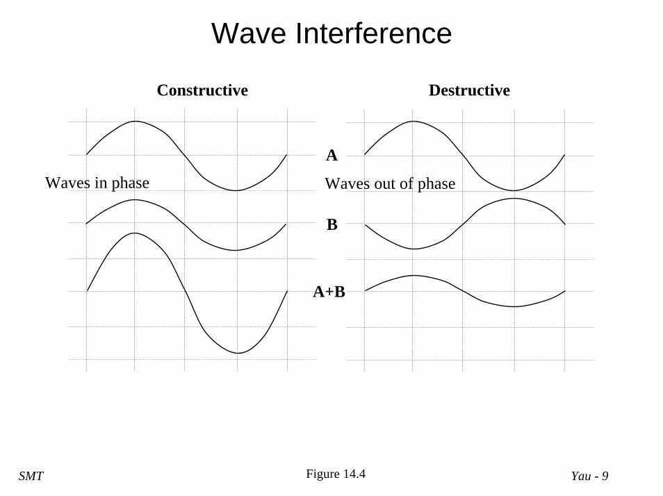
Wave Interference
A
B
A+B
Waves in phase Waves out of phase
Constructive Destructive
Figure 14.4

Yau - 10SMT
Optical Filtration
Secondary reflections (interference)
Coating 1 (non-reflecting)
Coating 3
Glass
Coating 2
Reflected wavelengths
Transmitted wavelength
Broadband light
Figure 14.5

Yau - 11SMT
Ultraviolet Spectrum
λ (nm)
7004 550 600 65050045040035030025020015010050
Ultraviolet spectrum Visible spectrum
Mercury lampExcimer laser
Photolithography light sources
ghi365 40524819313 436157126
Violet RedBlue Green Yellow OrangeMid-UVEUV DUVVUV
Figure 14.6
Yau - 12SMT
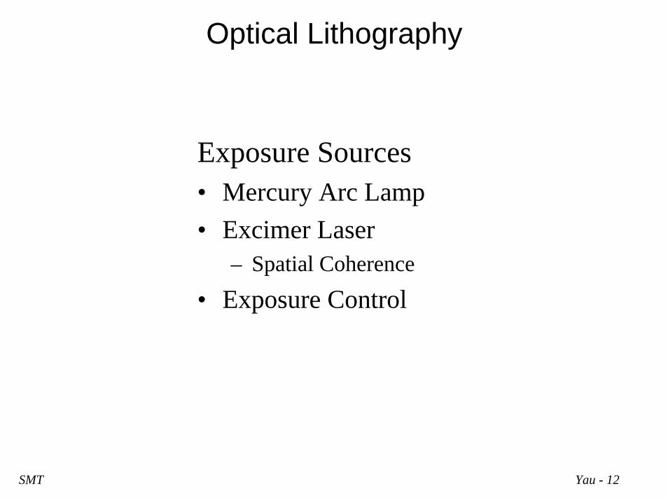
Optical Lithography
Exposure Sources• Mercury Arc Lamp• Excimer Laser
– Spatial Coherence
• Exposure Control
Yau - 13SMT
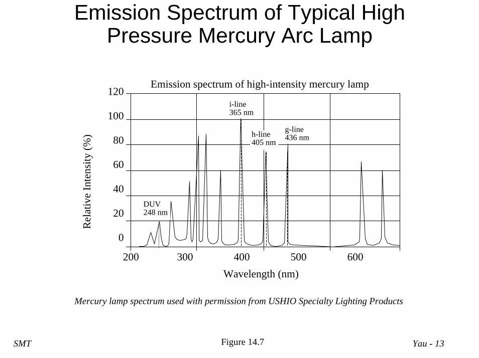
Emission Spectrum of Typical High Pressure Mercury Arc Lamp
120
100
80
60
40
20
0
200 300 400 500 600Wavelength (nm)
Rel
ativ
e In
tens
ity (%
) h-line405 nm
g-line436 nm
i-line365 nm
DUV248 nm
Emission spectrum of high-intensity mercury lamp
Mercury lamp spectrum used with permission from USHIO Specialty Lighting Products
Figure 14.7

Yau - 14SMT
Mercury Arc Lamp Intensity Peaks
UV Light Wavelength (nm) Descriptor CD Resolution (µm)
436 g-line 0.5405 h-line 0.4365 i-line 0.35248 Deep UV
(DUV)0.25
Table 14.2
Yau - 15SMT
Spectral Emission Intensity of 248 nm Excimer Laser vs. Mercury Lamp
100
80
60
40
20
0
Rel
ativ
e In
tens
ity (%
)
KrF laser
280210 240 260220
Wavelength (nm)
Hg lamp
Figure 14.8

Yau - 16SMT
Excessive Resist Absorption of Incident Light
Photoresist (after develop)
Substrate
Sloping profile
Figure 14.9
Yau - 17SMT
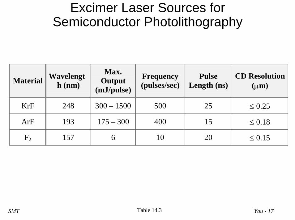
Excimer Laser Sources for Semiconductor Photolithography
Material Wavelength (nm)
Max.Output
(mJ/pulse)
Frequency(pulses/sec)
PulseLength (ns)
CD Resolution(µm)
KrF 248 300 – 1500 500 25 ≤ 0.25
ArF 193 175 – 300 400 15 ≤ 0.18
F2 157 6 10 20 ≤ 0.15
Table 14.3

Yau - 18SMT
Spatial Coherence
Incoherent light sourceof a single wavelength
Slit
Coherent cylindrical wave front
Two coherent cylindrical wave fronts
Interference patterns
Two slitsclosely spaced
Black box illuminator
Figure 14.10

Yau - 19SMT
Optical Lithography
Optics• Reflection of Light• Refraction of Light• Lens• Diffraction• Numerical Aperture, NA• Antireflective Coating
Yau - 20SMT
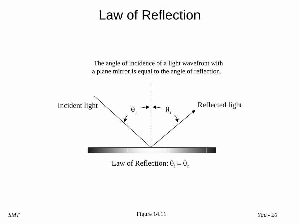
Law of Reflection
θi θrIncident light Reflected light
Law of Reflection: θi = θr
The angle of incidence of a light wavefront with a plane mirror is equal to the angle of reflection.
Figure 14.11

Yau - 21SMT
Application of Mirrors
Used with permission from Canon USA
Mask
Flat mirror
Ellipsoidal mirror
Flat mirror
Illuminator for a simple aligner
Figure 14.12

Yau - 22SMT
Refraction of Light Based on Two Mediums
• Snell’s Law: sin θi = n sin θr
• Index of refraction, n = sin θi / sin θr
θθair (n ≅ 1.0)
glass (n = 1.5)
fast medium
slow medium
θθ
air (n ≅ 1.0)
glass (n = 1.5)
fast medium
slow medium
Figure 14.13

Yau - 23SMT
Absolute Index of Refraction for Select Materials
Material Index of Refraction (n)
Air 1.000293
Water 1.33
Fused Silica (AmorphousQuartz)
1.458
Diamond 2.419
Table 14.4

Yau - 24SMT
Optical System of Lenses
Mercury lamp
Lamp position knob
Lamp monitor
Ellipsoidal mirror
Shutter
Fly’s eye lens
Flat mirror
Masking unitMirror
MirrorCollimator lens
Condenser lensCondenser lens
Optical filter
Fiber optics
Reticle
Reticle stage (X, Y, θ)
Projection optics
Optical focus sensor
Interferometer mirrorX-drive motor
Y-drive motor
θ-Z drive stage
Vacuum chuck
Wafer stage assembly
Light sensorIll
umin
ator a
ssem
bly
Figure 14.14Used with permission from Canon U.S.A., FPA-2000 i1 exposure system

Yau - 25SMT
Converging Lens with Focal Point
OF F’ S’S
f
2f f = focal lengthF = focal pointS = 2fO = origin, center of lens
Real image
Object
Figure 14.15
Yau - 26SMT
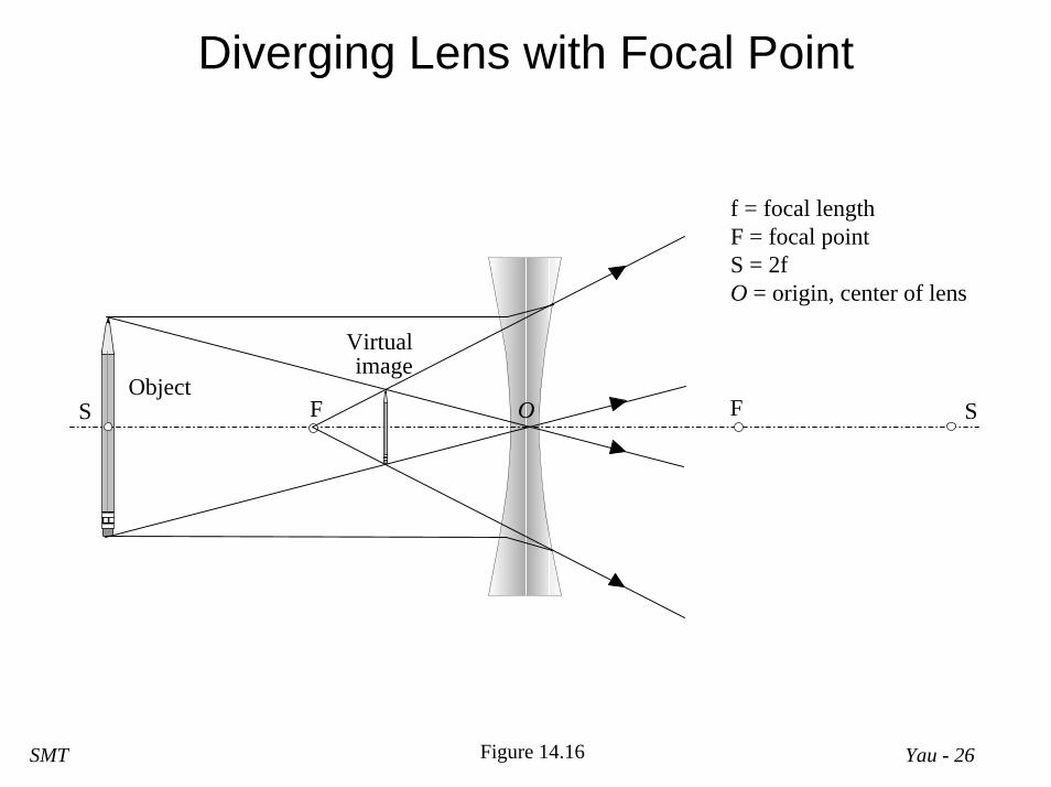
Diverging Lens with Focal Point
OF F’ S’S
Virtual image
Object
f = focal lengthF = focal pointS = 2fO = origin, center of lens
Figure 14.16
Yau - 27SMT
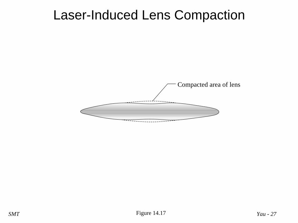
Laser-Induced Lens Compaction
Compacted area of lens
Figure 14.17

Yau - 28SMT
Interference Pattern from Light Diffraction at Small Opening
• Light travels in straight lines.• Diffraction occurs when light hits edges of objects.• Diffraction bands, or interference patterns, occur when light waves
pass through narrow slits.
Diffraction bands
Figure 14.18

Yau - 29SMT
Diffraction in a Reticle Pattern
Slit
Diffracted light rays
Plane light wave
Figure 14.19

Yau - 30SMT
Lens Capturing Diffracted Light
UV
0
12
3
4
12
3
4
Lens
Quartz
Chrome Diffraction patterns
Mask
Figure 14.20

Yau - 31SMT
Effect of Numerical Aperture on Imaging
Exposure light
Lens NA
Pinhole masks
Image results
Diffracted light
Good
Bad
Poor
Figure 14.21

Yau - 32SMT
Typical NA Values for Photolithography Tools
Type of Equipment NA Value
Scanning Projection Aligner with mirrors(1970s technology) 0.25
Step-and-Repeat 0.60 – 0.68
Step-and-Scan 0.60 – 0.68
Table 14.5

Yau - 33SMT
Photoresist Reflective Notching Due to Light Reflections
Polysilicon
Substrate
STISTI
UV exposure light
Mask
Exposed photoresist
Unexposed photoresist
Notched photoresist
Edgediffraction
Surfacereflection
Figure 14.22

Yau - 34SMT
Incident and Reflected Light Wave Interference in Photoresist
Standing waves cause nonuniform exposure along the thickness of the photoresist film.
Incident wave
Reflected wave
PhotoresistFilm
Substrate
Figure 14.23

Yau - 35SMT
Effect of Standing Waves in Photoresist
Photograph courtesy of the Willson Research Group, University of Texas at Austin
Photo 14.1

Yau - 36SMT
Antireflective Coating to Prevent Standing Waves
The use of antireflective coatings, dyes, and filters can help prevent interference.
Incident wave Antireflective coating
PhotoresistFilm
Substrate
Figure 14.24

Yau - 37SMT
Light Suppression with Bottom Antireflective Coating
BARCPolysilicon
Substrate
STISTI
UV exposure light
Mask
Exposed photoresist
Unexposed photoresist
Figure 14.25

Yau - 38SMT
BARC Phase-Shift Cancellation of Light
(A) Incident light
Photoresist
BARC (TiN)Aluminum
C and D cancel due to phase difference
(B) Top surface reflection
(C)(D)
Figure 14.26
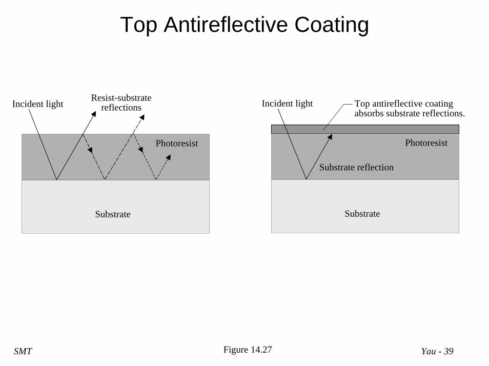
Yau - 39SMT
Top Antireflective Coating
Incident light
Photoresist
Resist-substrate reflections
Substrate
Incident light
Photoresist
Substrate reflection
Substrate
Top antireflective coating absorbs substrate reflections.
Figure 14.27

Yau - 40SMT
Optical Lithography
Resolution• Calculating Resolution• Depth of Focus• Resolution Versus Depth of Focus
– Surface Planarity

Yau - 41SMT
Resolution of Features
2.0
1.0
0.5
0.10.25
The dimensions of linewidths and spaces must be equal. As feature sizes decrease, it is more difficult to separate features from each other.
Figure 14.28

Yau - 42SMT
Calculating Resolution for a given λ, NA and k
Lens, NA
Wafer
Mask
Illuminator, λ
R
k = 0.6
λ ΝΑ R365 nm 0.45 486 nm365 nm 0.60 365 nm193 nm 0.45 257 nm193 nm 0.60 193 nm
i-line
DUV
k λNAR =
Figure 14.29
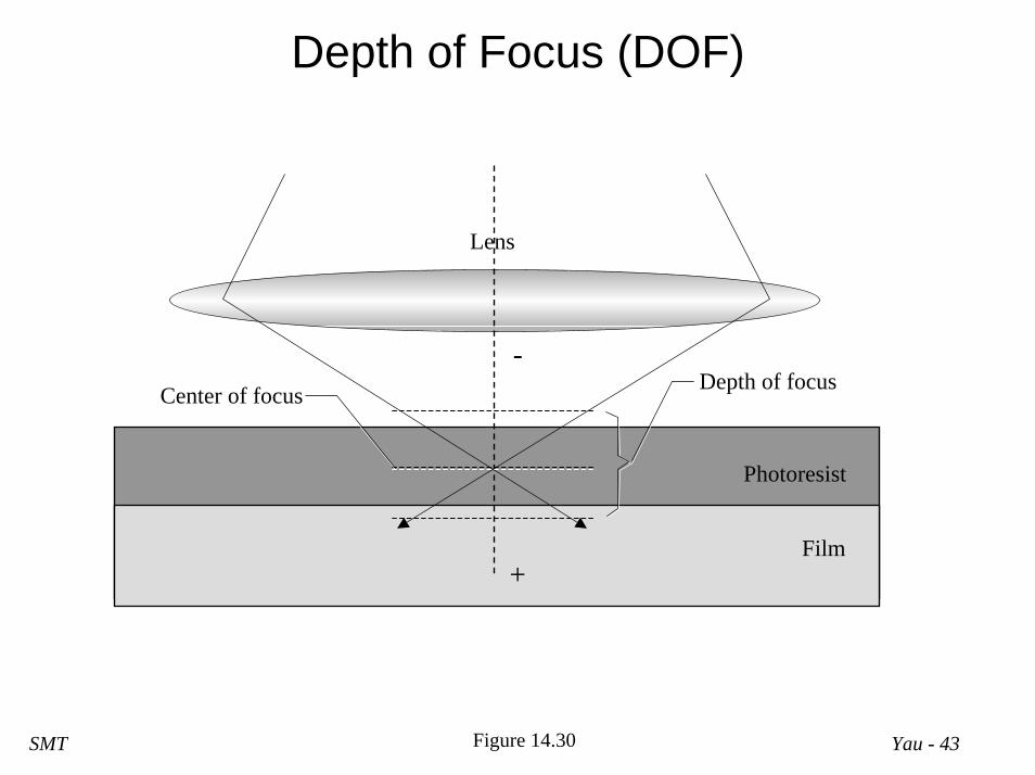
Yau - 43SMT
Depth of Focus (DOF)
+
-
Photoresist
Film
Depth of focusCenter of focusCenter of focus
Lens
Figure 14.30

Yau - 44SMT
Resolution Versus Depth of Focus for Varying NA
λ 2(NA)2DOF =
Photoresist
Film
Depth of focusDepth of focusCenter of focus
++
--Lens, NA
Wafer
Mask
Illuminator, λ
DOF
λ ΝΑ R DOF365 nm 0.45 486 nm 901 nm365 nm 0.60 365 nm 507 nm193 nm 0.45 257 nm 476 nm193 nm 0.60 193 nm 268 nm
i-line
DUV
Figure 14.31

Yau - 45SMT
Photolithograhy Equipment
• Contact Aligner• Proximity Aligner• Scanning Projection Aligner (scanner)• Step-and-Repeat Aligner (stepper)• Step-and-Scan System

Yau - 46SMT
Contact/Proximity Aligner System
Illuminator
Alignment scope (split
vision)Mask
Wafer
Vacuum chuck
Mask stage (X, Y , Z , θ)
Wafer stage (X, Y, Z, θ)
Mercury arc lamp
Used with permission from Canon USA, Figure 14.32

Yau - 47SMT
Edge Diffraction and Surface Reflectivity on Proximity Aligner
UV
Mask
Diffraction of light on edges results in reflections from underside of mask causing undesirable resist exposure.
UV exposure light
Substrate
Resist
Diffracted and reflected light
Gap
Mask
Substrate
Figure 14.33

Yau - 48SMT
Scanning Projection Aligner
Redrawn and used with permission from Silicon Valley Group Lithography
Mask
Wafer
Mercury arc lamp
Illuminator assembly
Projection optics assembly
Scan direction
Exposure light(narrow slit of UV
gradually scans entire mask field onto wafer)
Figure 14.34

Yau - 49SMT
Step-and-Repeat Aligner (Stepper)
Used with permission from Canon USA, FPA-3000 i5 (original drawing by FG2, Austin, TX)
Figure 14.35
Yau - 50SMT
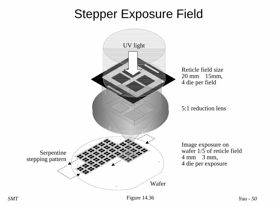
Stepper Exposure Field
UV light
Reticle field size20 mm × 15mm,4 die per field
5:1 reduction lens
Wafer
Image exposure on wafer 1/5 of reticle field4 mm × 3 mm,4 die per exposure
Serpentine stepping pattern
Figure 14.36
Yau - 51SMT
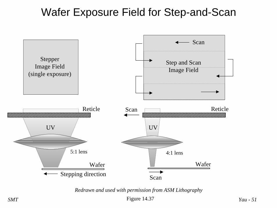
Wafer Exposure Field for Step-and-Scan
5:1 lens
UVUV
Step and ScanImage Field
Scan
StepperImage Field
(single exposure)
4:1 lens
ReticleReticle Scan
Scan
Wafer WaferStepping direction
Redrawn and used with permission from ASM LithographyFigure 14.37
Yau - 52SMT
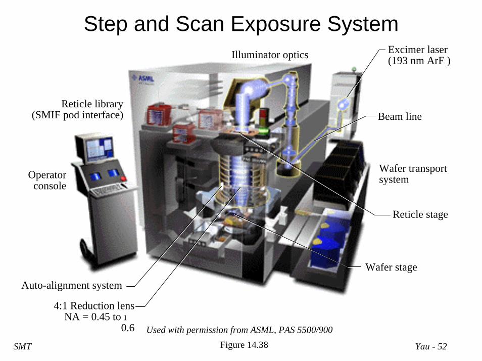
Step and Scan Exposure SystemIlluminator optics
Beam line
Excimer laser (193 nm ArF )
Operator console
4:1 Reduction lensNA = 0.45 to
0.6
Wafer transport system
Reticle stage
Auto-alignment system
Wafer stage
Reticle library (SMIF pod interface)
Used with permission from ASML, PAS 5500/900Figure 14.38
Yau - 53SMT
Reticles
• Comparison of Reticle Versus Mask• Reticle Materials• Reticle Reduction and Size• Reticle Fabrication• Sources of Reticle Damage
Yau - 54SMT
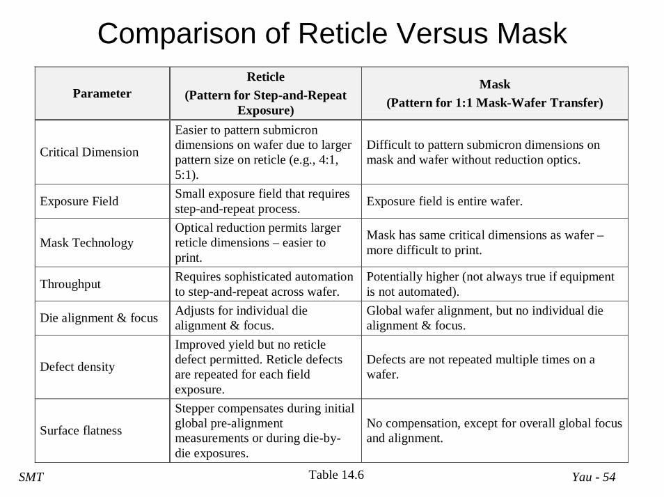
Comparison of Reticle Versus Mask
ParameterReticle
(Pattern for Step-and-RepeatExposure)
Mask(Pattern for 1:1 Mask-Wafer Transfer)
Critical Dimension
Easier to pattern submicrondimensions on wafer due to largerpattern size on reticle (e.g., 4:1,5:1).
Difficult to pattern submicron dimensions onmask and wafer without reduction optics.
Exposure Field Small exposure field that requiresstep-and-repeat process. Exposure field is entire wafer.
Mask TechnologyOptical reduction permits largerreticle dimensions – easier toprint.
Mask has same critical dimensions as wafer –more difficult to print.
Throughput Requires sophisticated automationto step-and-repeat across wafer.
Potentially higher (not always true if equipmentis not automated).
Die alignment & focus Adjusts for individual diealignment & focus.
Global wafer alignment, but no individual diealignment & focus.
Defect density
Improved yield but no reticledefect permitted. Reticle defectsare repeated for each fieldexposure.
Defects are not repeated multiple times on awafer.
Surface flatness
Stepper compensates during initialglobal pre-alignmentmeasurements or during die-by-die exposures.
No compensation, except for overall global focusand alignment.
Table 14.6
Yau - 55SMT
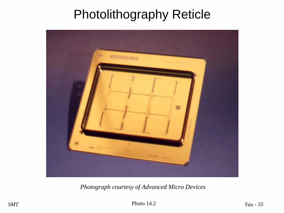
Photolithography Reticle
Photograph courtesy of Advanced Micro Devices
Photo 14.2

Yau - 56SMT
Comparison of Reticle Reduction Versus Exposure Field
Field size on reticle
Projection lens
Exposure field on wafer
Lens Type 10:1 5:1 4:1 1:1
Reticle FieldSize (mm)
100 100 100 100 100 100 30 30
Exposure Fieldon Wafer (mm)
10 10 20 20 25 25 30 30
Die per Field ofExposure(assume 5mm 5mm die size)
4 16 25 36
Figure 14.39

Yau - 57SMT
Principles of Electron Beam Lithography
Work chamber, load chamber,vibration isolation, ion pump, and vacuum system
Work Station
Transfer and drive
Stage position control
Height deflection
and dynamic
correction
Vacuum control module
TFE electron source control
Electron beam controlServo control
Operator console
9-track magnetic tape drive
Control computer
Super flash HTM
Printer/Plotter
Electronics Console
Data direct computer
Height detection assembly
Work table
Beam control and deflection
TFE electron beam column
Automatic loading chamberWork stage
Dynamic corrections
Utility Console
Cassette clamping control
Temperature control
Coolant flow
control
Air and nitrogen control
Water chiller
Backing pump
Roughing pump
Used with permission from Etec Systems, Inc., MEBES 4500 SystemsFigure 14.40

Yau - 58SMT
Pellicle on a Reticle
The particle on the pellicle surface is outside of optical focal range.
Antireflective coatings Pellicle film
Chrome patternDepth of focus
Mask material
Reticle
Pellicle film
Frame
Chrome pattern
Figure 14.41

Yau - 59SMT
Optical Enhancement Techniques
• Phase-Shift Mask (PSM)• Optical Proximity Correction (OPC)• Off-Axis Illumination • Bias

Yau - 60SMT
Phase-Shifting Mask
b) APSMa) BIM c) Rim PSM
Chrome Absortive phase shifters
Rim phase shifters
Blockers
-1
+10
-1
+10
+10
Intensity on wafer
Electric field on
mask
Electric field on
wafer
Reprinted from the January 1992 edition of Solid State Technology, copyright 1992 by PennWell Publishing Company
Figure 14.42
Yau - 61SMT
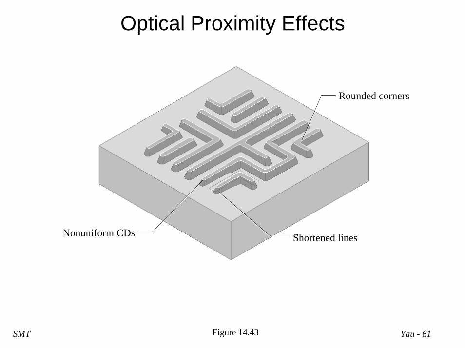
Optical Proximity Effects
Rounded corners
Nonuniform CDs Shortened lines
Figure 14.43

Yau - 62SMT
Off-Axis Illumination
A
B- A+
B+B+A-A-
BOff-axis illumination
(b)
Conventional illumination (on-axis)
- Order diffraction
+ Order diffraction
(a)
Pinhole mask
Projection optics
Wafer
Figure 14.44
Yau - 63SMT
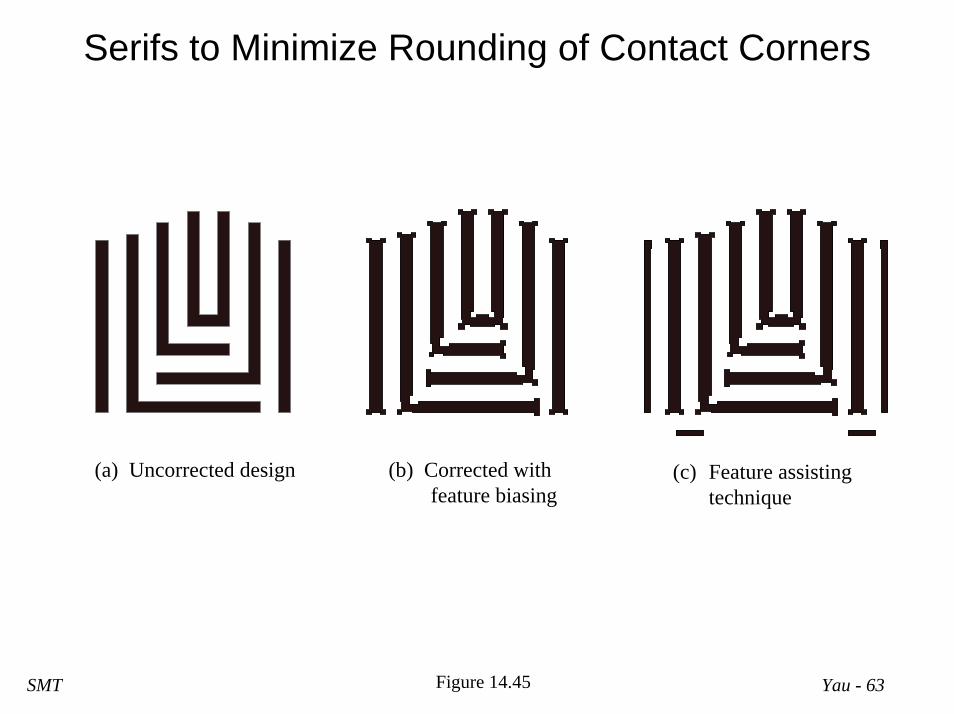
Serifs to Minimize Rounding of Contact Corners
(b) Corrected with feature biasing
(a) Uncorrected design (c) Feature assisting technique
Figure 14.45

Yau - 64SMT
Alignment
• Baseline Compensation• Overlay Accuracy• Alignment Marks• Types of Alignment
Yau - 65SMT
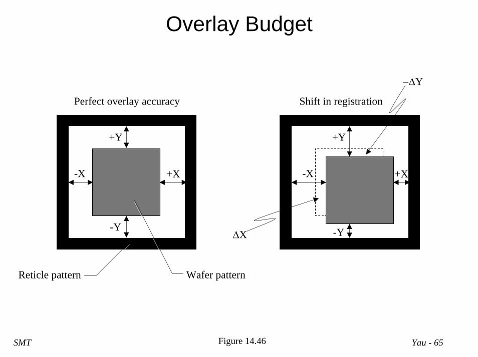
Overlay Budget
-X +X
+Y
-Y∆X
−∆Y
Shift in registration
-X +X
+Y
-Y
Wafer patternReticle pattern
Perfect overlay accuracy
Figure 14.46

Yau - 66SMT
Grid of Exposure Fields on Wafer
1 2 3 4
11 12 13 14 15 16
10 9 8 7 6 5
23 24 25 26 27 28
22 21 20 19 18 17
32 31 30 29
Start
Stop
Figure 14.47

Yau - 67SMT
Step-and-Repeat Alignment System
Used with permission from Canon USA, FPA-2000 i1
Figure 14.48

Yau - 68SMT
Alignment Marks
2nd Mask
1st Mask
2nd mask layer
1st mask layer
RA, Reticle alignment marks, L/RGA, Wafer global alignment marks, L/RFA, Wafer fine alignment marks, L/R
+ +++
RAL
RAR+ GA
+ FAL
+ FAR
+ GAR
+ GAL
Notch, coarse alignment
FAL
FAR
FAL/R +
+FAL/R +
For 2nd mask
+ From 1st mask
{
Figure 14.49

Yau - 69SMT
On-Axis Versus Off-Axis Alignment System
Alignmentlaser (633 nm)
Optical fiber
Video
Off-axisalignment unit
Alignment BLC fiducial
Off-Axis Alignment System
Alignmentlaser (633 nm)
Microscope objectives for video camera
Projection optics
Wafer stage
Alignment BLC fiducial
Reticle
On-Axis Alignment System
Used with permission from Canon USA, redrawn after FPA-2000i1 schematics
Figure 14.50

Yau - 70SMT
Environmental Conditions
• Temperature• Humidity• Vibration• Atmospheric Pressure• Particle Contamination

Yau - 71SMT
Comparison of Photo Tools(Refer to Table 14.7)
• Models by Manufacturer• Wavelength (nm)• Type of Aligner• Illumination Type• Exposure Field Size (mm)• Resolution (µm)• Overlay Accuracy (nm)
Yau - 72SMT
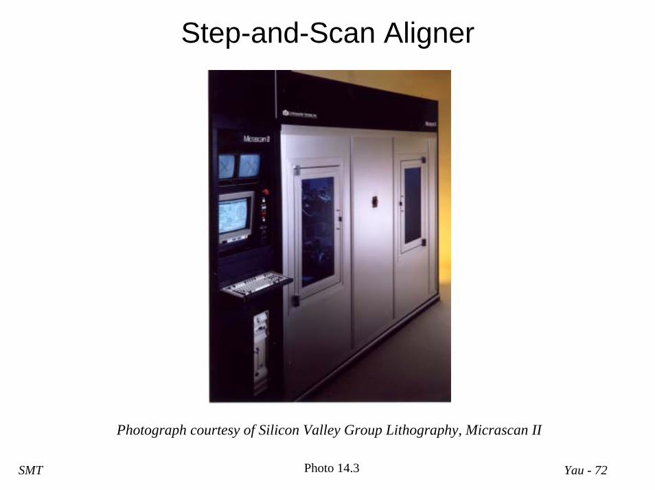
Step-and-Scan Aligner
Photograph courtesy of Silicon Valley Group Lithography, Micrascan II
Photo 14.3