photoelectron spectroscopy for surface analysis: x-ray...
TRANSCRIPT

MT.1
Photoelectron spectroscopy for surface
analysis: X-ray and UV excitation
Lorenzo Calvo-Barrio and Gardenia Vargas
Unitat d’Anàlisi de Superfícies, CCiTUB, Universitat de Barcelona. Lluís Solé i Sabarís, 1-3, 08028 Barcelona, Spain.
email: [email protected]
Abstract. This article summarizes the basic principles of photoelectron spectroscopy for surface analysis, with examples of applications in material
science that illustrate the capabilities of the related techniques.
Handbook of instrumental techniques from CCiTUB

Photoelectron spectroscopy for surface analysis
1
MT.1
1. 1. 1. 1. IntroductionIntroductionIntroductionIntroduction
Photoelectron Spectroscopy (PES) is a general term used to describe the characterization techniques that study the surface of a material by using either X-rays or ultraviolet (UV) light as an excitation source to promote an electronic emission. In both cases, the physical effect upon which these techniques are based is the same, the photoelectric effect, which can be traced back to its first documented observation by Hertz in 1887. During the first decades of the last century, the theory underlying this effect was quickly established together with the quantum theory, being Rutherford and Einstein [1] two of the well-known scientists who worked on its development. But it was not until the second half of the century that other researchers could develop some experimental devices that used the photoelectric effect to characterize the surface properties of materials. Those initial works culminated with a publication in 1967 by Kai Siegbahn [2], who explained how to obtain a spectrum by using X-rays as excitation source. At the same time, David W. Turner started to study free molecules in a gas phase by exciting them with ultraviolet light and collecting the emitted electrons. Since then, PES equipments have been built, their commercialization is in constant evolution and the technological parts, such as vacuum pumps, excitation sources, analyzers and electronics, are in continuous improvement. Nowadays, hundreds of PES spectrometers are being used in cutting edge technology research centres. Instruments combining both X-ray and UV excitation are not uncommon since, besides the excitation source, the remaining parts of the equipment are practically identical.
When X-ray excitation is used in PES, the technique is called XPS. It is also known as Electron Spectroscopy for Chemical Analysis (ESCA), given the use made of the emitted electrons. In short terms, XPS involves the irradiation with soft monochromatic X-rays of a solid in vacuum, and the subsequent emission and study of the electrons produced by photoelectric effect. The collected electrons can be represented in a plot where the number of electrons versus their kinetic or binding energy is drawn. The information obtained concerns only the surface of the material, because the mean free path of electrons in solids is so small that the detected electrons originate from a few top atomic layers. The achievement of quantitative measurements of the elemental composition and the identification of the different chemical states of the elements present at any surface are some of the main utilities of this technique.
On the other hand, the technique is called UPS when UV excitation is used in PES. Principles are essentially the same as those of XPS, but such a low-energy radiation (below 50 eV) is only capable of ionizing electrons from the outermost levels of atoms, the valence band (VB). Since these levels are directly involved in molecular bonding features, this technique is also known as molecular photoelectron spectroscopy. The study of the lower energy region of the spectra gives information about the density of occupied states (DOS) in the VB. Among other applications, this technique can be used to calculate the electronic band structure of a material and some relevant parameters concerning the interaction between interfaces.
2. 2. 2. 2. MethodologyMethodologyMethodologyMethodology
2.1. Basic Principles
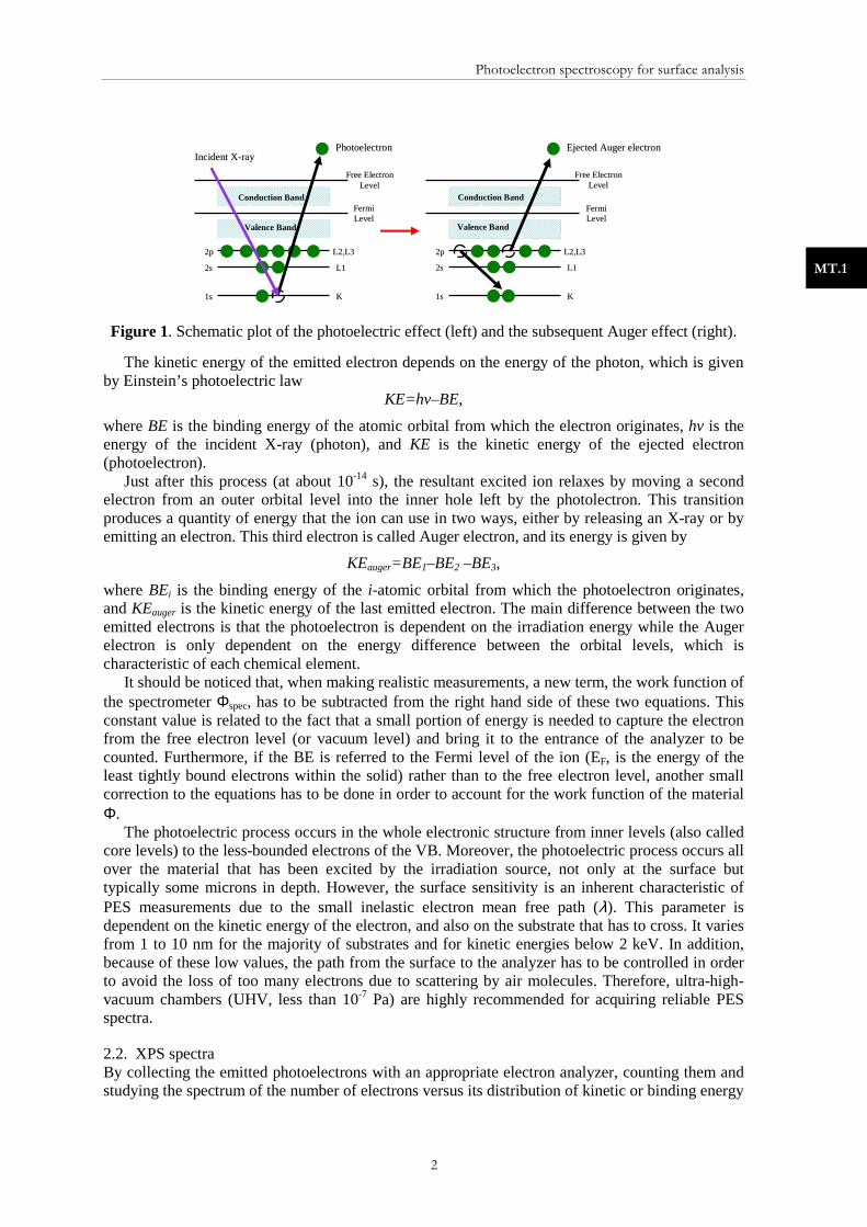
Electrons are arranged in orbital levels around the nucleus and are bound to it by electrostatic attraction. Each orbital level has discrete energy levels that differ in value from the same orbital level in atoms of different elements, due to the different electrostatic attraction to the nuclei with different number of protons. The amount of energy required to remove one electron from the atom (the energy of its orbital level) is directly the binding energy of the electron. Therefore, a short wavelength photon from a specific X-ray source can be used to irradiate and thus to ionize an atom, producing an ejected free electron which characterizes the atom, as shown in Figure 1.
Photoelectron spectroscopy for surface analysis
2
MT.1
The kinetic energy of the emitted electron depends on the energy of the photon, which is given by Einstein’s photoelectric law
KE=hv–BE,
where BE is the binding energy of the atomic orbital from which the electron originates, hv is the energy of the incident X-ray (photon), and KE is the kinetic energy of the ejected electron (photoelectron).
Just after this process (at about 10-14 s), the resultant excited ion relaxes by moving a second electron from an outer orbital level into the inner hole left by the photolectron. This transition produces a quantity of energy that the ion can use in two ways, either by releasing an X-ray or by emitting an electron. This third electron is called Auger electron, and its energy is given by
KEauger=BE1–BE2 –BE3,
where BEi is the binding energy of the i-atomic orbital from which the photoelectron originates, and KEauger is the kinetic energy of the last emitted electron. The main difference between the two emitted electrons is that the photoelectron is dependent on the irradiation energy while the Auger electron is only dependent on the energy difference between the orbital levels, which is characteristic of each chemical element.
It should be noticed that, when making realistic measurements, a new term, the work function of the spectrometer Φspec, has to be subtracted from the right hand side of these two equations. This constant value is related to the fact that a small portion of energy is needed to capture the electron from the free electron level (or vacuum level) and bring it to the entrance of the analyzer to be counted. Furthermore, if the BE is referred to the Fermi level of the ion (EF, is the energy of the least tightly bound electrons within the solid) rather than to the free electron level, another small correction to the equations has to be done in order to account for the work function of the material Φ.
The photoelectric process occurs in the whole electronic structure from inner levels (also called core levels) to the less-bounded electrons of the VB. Moreover, the photoelectric process occurs all over the material that has been excited by the irradiation source, not only at the surface but typically some microns in depth. However, the surface sensitivity is an inherent characteristic of PES measurements due to the small inelastic electron mean free path (λ). This parameter is dependent on the kinetic energy of the electron, and also on the substrate that has to cross. It varies from 1 to 10 nm for the majority of substrates and for kinetic energies below 2 keV. In addition, because of these low values, the path from the surface to the analyzer has to be controlled in order to avoid the loss of too many electrons due to scattering by air molecules. Therefore, ultra-high-vacuum chambers (UHV, less than 10-7 Pa) are highly recommended for acquiring reliable PES spectra.
2.2. XPS spectra By collecting the emitted photoelectrons with an appropriate electron analyzer, counting them and studying the spectrum of the number of electrons versus its distribution of kinetic or binding energy
Figure 1. Schematic plot of the photoelectric effect (left) and the subsequent Auger effect (right).
LL22,,LL33 LL11 KK
FFeerrmmii LLeevveell
FFrreeee EElleeccttrroonn LLeevveell
EEjjeecctteedd AAuuggeerr eelleeccttrroonn
11ss 22ss 22pp
Conduction Band Valence Band
Conduction Band Valence Band
LL22,,LL33 LL11 KK
FFeerrmmii LLeevveell
FFrreeee EElleeccttrroonn LLeevveell
IInncciiddeenntt XX--rraayy PPhhoottooeelleeccttrroonn
11ss 22ss 22pp

Photoelectron spectroscopy for surface analysis
3
MT.1
(using the former equation), it is possible to recognize the material they come from. The analysis of a wide range of BEs will provide unique signatures of the elements as a function of their atomic number, thus providing elemental analysis. Moreover, if a mixture of elements is present, BE information will be related to all the elements and to their concentration ratio (the spectrum of a mixture of elements is approximately the sum of the spectra of the individual components). In this case a new problem arises: to determine the element from which a specific electron belongs, because overlapping of orbital levels from different elements could appear. This difficulty can be solved by looking for all the other orbital levels to know if the element is present or not.
The main features of a XPS spectrum of elemental uranium excited by a 1486.6 eV AlKα monochromatic X-ray line are shown in Figure 2. First of all, primary peaks resulting from the photoelectron process (a) can be seen. Some of them are in groups of two peaks as a consequence of the spin-orbit splitting (degeneration) that takes place in all orbital levels except in the s one. The intensity ratio between the two peaks depends only on the angular momentum 1 of the orbital level, but the distance between them depends also on the atomic number Z. The width of every primary peak depends quadratically on three contributions, one related to the physical nature of the atoms, another one concerning the analyzer characteristics, and a final one produced by the excitation source. The physical contribution cannot be modified because it originates from Heisenberg’s uncertainty principle [3], but the two others can be reduced by improving the technique methodology.
Figure 2. XPS spectrum of elemental uranium.
The characteristic background (b) of the XPS spectrum is mainly due to the inelastically
scattered electrons. The electrons excited by the X-ray source at a certain depth not too far from surface cannot leave the surface without losing kinetic energy by inelastic scattering with atoms of the solid. This random energy loss appears in the spectrum as an increase of the background for binding energies greater than each primary peak.
The Auger electrons (c) can also be detected in the spectrum. Some Auger transitions can be seen, but the energy position is not relevant because the transitions do not dependent on the irradiation energy. They appear as a broad band because they are the result of the different combinations of energy losses from electrons of two or three different orbital levels.
Second order features of the XPS spectra (d) worth pointing out are: peaks due to the X-ray satellites of the excitation sources, shake-up and shake-off satellites, multiple splitting and asymmetric metal levels (all them related to the reorganization in different ways of the VB when the photoelectron leaves the surface), and bulk and surface plasmons (related to excitation of the modes of collective oscillation in the sea of conduction electrons). All these features can change dramatically the aspect of a high resolution (HR) spectrum for a selected BE window.
Finally, it is known that the interactions between atoms which form the different types of chemical bonds in molecules and compounds depend only on the VB levels, while the core levels are not directly involved in the bonding process. However, according to Koopmans' theorem, if the energy of the initial state of the atom changes by the formation of a chemical bond, the BE of the core electrons will change in a fixed quantity equal to the difference in the two atom states
1000 800 600 400 200 0
b
dc
a
Inte
nsity
(a.
u.)
Binding Energy (eV)
Photoelectron spectroscopy for surface analysis
4
MT.1
∆BE= ∆(Einitial(n)–Efinal (n-1)),
being n the number of electrons that remains in the atom or ion. The fact that one type of bound or another is formed will affect slightly enough the electron bounded to the core level so as to observe changes when studying its energy at high enough resolution. Thus, chemical information can be extracted from XPS spectra by a HR spectrum fitting for determining the amount of each type of bond present in the elements of the surface. The level of accuracy when determining the zero of energy is of vital importance and this is a particularly difficult parameter to fix. Sometimes it is possible to measure where electrons start to be counted and equal this energy level to zero, but usually it is better to use an internal calibration, such as the position of one peak not affected by chemical bonding at the surface. For this purpose adventitious carbon (C) present by atmospheric contamination is very useful, and 284.8 eV can be fixed as an energy reference [4].
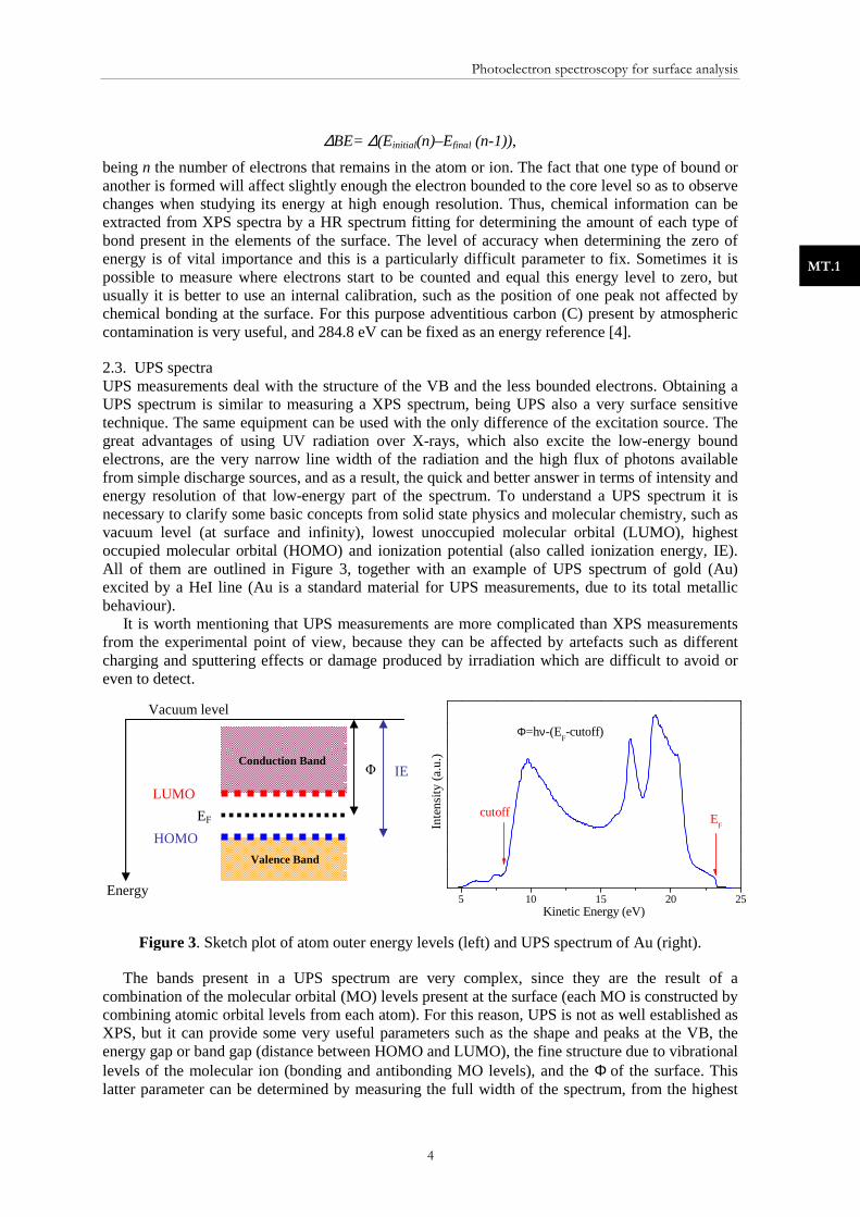
2.3. UPS spectra UPS measurements deal with the structure of the VB and the less bounded electrons. Obtaining a UPS spectrum is similar to measuring a XPS spectrum, being UPS also a very surface sensitive technique. The same equipment can be used with the only difference of the excitation source. The great advantages of using UV radiation over X-rays, which also excite the low-energy bound electrons, are the very narrow line width of the radiation and the high flux of photons available from simple discharge sources, and as a result, the quick and better answer in terms of intensity and energy resolution of that low-energy part of the spectrum. To understand a UPS spectrum it is necessary to clarify some basic concepts from solid state physics and molecular chemistry, such as vacuum level (at surface and infinity), lowest unoccupied molecular orbital (LUMO), highest occupied molecular orbital (HOMO) and ionization potential (also called ionization energy, IE). All of them are outlined in Figure 3, together with an example of UPS spectrum of gold (Au) excited by a HeI line (Au is a standard material for UPS measurements, due to its total metallic behaviour).
It is worth mentioning that UPS measurements are more complicated than XPS measurements from the experimental point of view, because they can be affected by artefacts such as different charging and sputtering effects or damage produced by irradiation which are difficult to avoid or even to detect.
Figure 3. Sketch plot of atom outer energy levels (left) and UPS spectrum of Au (right).
The bands present in a UPS spectrum are very complex, since they are the result of a combination of the molecular orbital (MO) levels present at the surface (each MO is constructed by combining atomic orbital levels from each atom). For this reason, UPS is not as well established as XPS, but it can provide some very useful parameters such as the shape and peaks at the VB, the energy gap or band gap (distance between HOMO and LUMO), the fine structure due to vibrational levels of the molecular ion (bonding and antibonding MO levels), and the Φ of the surface. This latter parameter can be determined by measuring the full width of the spectrum, from the highest
5 10 15 20 25
Inte
nsi
ty (
a.u.
)
Kinetic Energy (eV)
cutoff EF
Φ=hν-(EF-cutoff)
Energy
Vacuum level
Conduction Band
Valence Band
HOMO
LUMO
EF
Φ IE

Photoelectron spectroscopy for surface analysis
5
MT.1
kinetic energy (EF) to the lowest kinetic energy cutoff, and then by subtracting the photon energy of the exciting radiation. For this purpose, it is necessary to measure accurately the energy cutoff (also called the onset of secondary electrons or onset of photoemission), defined as the minimum kinetic energy for which electrons are detected [5].
2.4. Analysis capabilities: Quantification, angle resolved and in-depth (profile) analysis 2.4.1. Quantification. XPS can be considered as a quantitative technique, because the relative atomic concentration of the different constituents can be determined in elemental percentage. The number of electrons produced by photoelectric effect depends not only on the quantity of chemical elements present, but also on the ionization cross section of the orbital level (the probability that an ionization is produced) and other geometrical and analyzer parameters. The most common method used for quantification is the relative sensitivity factor (RSF) method, which supposes that
I=n·Fs and Fs=f·σ·θ·y·λ·A·T,
where I is the intensity (or the area) of a photoelectric peak of a given element, n is the number of atoms per cm3 of the element in the sample and Fs is a constant value called sensitivity factor. Fs depends on the X-ray flux in photons/cm2·sec f, the photoelectric cross section for the atomic orbital of interest in cm2 σ, the angular efficiency factor for the instrumental arrangement based on the angle between the photon path and detected electron θ, the efficiency in the photoelectric process for formation of photoelectrons of the normal photoelectron energy y, the λ, the area of the sample from which photoelectrons are detected A, and the detection efficiency for electrons emitted from the sample T. Thus, if all elements present at the surface are detected and one peak of each element with its well known Fs can be chosen, the following equation can be established
where Cx is the concentration of one element in percentage present at the surface.
This method is currently used and software programs and databases are available [6]. Nevertheless, it has also some drawbacks namely it does not work for inhomogeneous structures in the nanometric scale, or some Fs values are not well established (they are far from being constant or simply do not exist for some photoelectric peaks of several elements). Another approach less used for quantification is to simulate theoretical spectra and then to compare them with the experimental results, paying special attention to the background [7].
2.4.2. Angle resolved XPS (ARXPS). ARXPS measurements define the sample tilting with respect to the analyzer. Changes in the design source-sample-analyzer will affect the escape depth of the electrons. Tilting the sample towards the analyzer will improve the relative signal from the outer part of the surface (from 1 to 2 nm) in front of the inner part, but will decrease in global terms the total amount of collected intensity. Moreover, the thickness of very thin overlayers of the surface (less than 5 nm) can be determined by assuming knowledge of some parameters. For this reason, the technique is sometimes called non-destructive depth profiling. The simplest approach to this calculation is to assume that the intensity of the collected electrons that come specifically from the substrate material below the overlayer Is can be expressed by the following equation
Is=I o·e-d/(λcosθ),
where Io is the measured intensity if there was no overlayer on the substrate, d is the thickness of the overlayer and θ is the angle between the normal to the surface and the analyzer (take off angle). More complex attempts can be done to increase accuracy in these calculations, and to study either a heterogeneous layer or a multilayer on a substrate [8].
2.4.3. In-depth XPS. The erosion of the surface under UHV conditions allows to perform in-depth measurements. For this purpose an ion gun of a noble gas such as argon (Ar) is sputtered over the surface. Measurements alternate with the sputtering and, as a consequence, a new surface is present for the analysis every time. Thus, an elemental profile can be drawn. By controlling both intensity
Cx = = Nx Ix / Fs
Σ ni Σ I i / Fi ,Cx = =
Nx Ix / Fs
Σ ni Σ I i / Fi ,
and energy from the ions, the damage produced by the sputtering and the chemical interthe implanted ions can be minimizedsome elements with enough resolution to obtain a chemical state profile
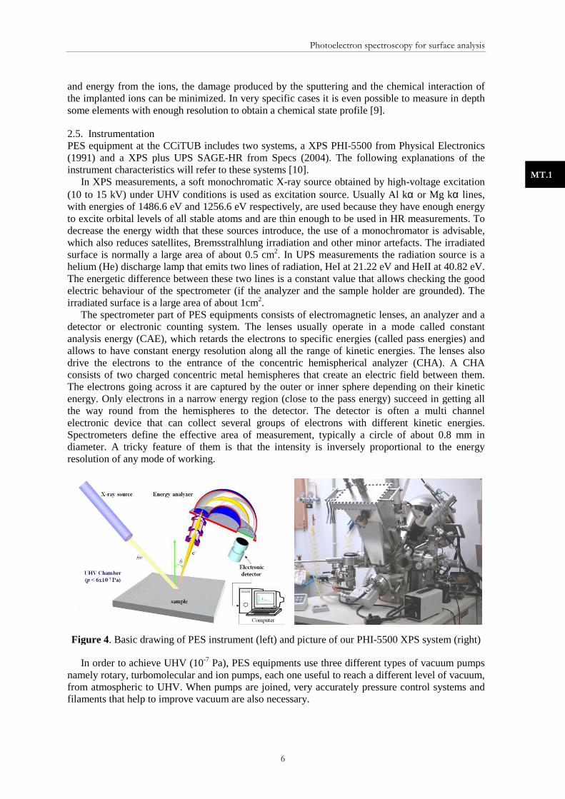
2.5. Instrumentation PES equipment at the CCiTUB incl(1991) and a XPS plus UPS SAGEinstrument characteristics will refer
In XPS measurements, a soft monochromati(10 to 15 kV) under UHV conditions is used as excitation source. Usually Alwith energies of 1486.6 eV and 1256.6 eV to excite orbital levels of all stable atoms and are thin enough to be used in HR measurements. To decrease the energy width that these which also reduces satellites, Bremsurface is normally a large area of about 0.5 cmhelium (He) discharge lamp that emits twoThe energetic difference between these two lines is a constant value that allows checking the good electric behaviour of the spectrometer (if the analyzer and the sample holder are grounded). The irradiated surface is a large area of about 1cm
The spectrometer part of PES equipments consists of electromagnetic lenses, an analyzer and a detector or electronic counting system. The lenses usually operate in a mode called constant analysis energy (CAE), which retards the electrons to specific energiallows to have constant energy resolution along all the range of kinetic energies. The lenses also drive the electrons to the entrance of the concentric hemispherical analyzer (CHA). A CHA consists of two charged concentric meThe electrons going across it are captured by the outer or inner sphere depending on their kinetic energy. Only electrons in a narrow energy region (close to the pass energy) succeed in getting althe way round from the hemispheres to the detector. The detector is often a multi channel electronic device that can collect several groups of electrons with different kinetic energies. Spectrometers define the effective area of measurement, typicdiameter. A tricky feature of them is that the intensity is inversely proportional to the energy resolution of any mode of working.
Figure 4. Basic drawing of PES instrument (left) and picture of our PHI
In order to achieve UHV (10-
namely rotary, turbomolecular and ion pumps, each one useful to reach a different level of vacuumfrom atmospheric to UHV. When pumps are jfilaments that help to improve vacuum are also necessary.
Photoelectron spectroscopy for surface analysis
6
and energy from the ions, the damage produced by the sputtering and the chemical intercan be minimized. In very specific cases it is even possible to measure in depth
lution to obtain a chemical state profile [9].
includes two systems, a XPS PHI-5500 from PhyXPS plus UPS SAGE-HR from Specs (2004). The following expla
refer to these systems [10]. In XPS measurements, a soft monochromatic X-ray source obtained by high-
(10 to 15 kV) under UHV conditions is used as excitation source. Usually Al kα86.6 eV and 1256.6 eV respectively, are used because they have enough energy
to excite orbital levels of all stable atoms and are thin enough to be used in HR measurements. To these sources introduce, the use of a monochromat
ch also reduces satellites, Bremsstralhlung irradiation and other minor artefacts. The irradiated surface is normally a large area of about 0.5 cm2. In UPS measurements the radiation source is a
discharge lamp that emits two lines of radiation, HeI at 21.22 eV and HeII at 40.82 eV. The energetic difference between these two lines is a constant value that allows checking the good electric behaviour of the spectrometer (if the analyzer and the sample holder are grounded). The rradiated surface is a large area of about 1cm2.
The spectrometer part of PES equipments consists of electromagnetic lenses, an analyzer and a detector or electronic counting system. The lenses usually operate in a mode called constant analysis energy (CAE), which retards the electrons to specific energies (called pass energies) and allows to have constant energy resolution along all the range of kinetic energies. The lenses also drive the electrons to the entrance of the concentric hemispherical analyzer (CHA). A CHA consists of two charged concentric metal hemispheres that create an electric field between them. The electrons going across it are captured by the outer or inner sphere depending on their kinetic energy. Only electrons in a narrow energy region (close to the pass energy) succeed in getting althe way round from the hemispheres to the detector. The detector is often a multi channel electronic device that can collect several groups of electrons with different kinetic energies. Spectrometers define the effective area of measurement, typically a circle of about 0.8 mm in
of them is that the intensity is inversely proportional to the energy resolution of any mode of working.
of PES instrument (left) and picture of our PHI-5500 XPS system (righ
-7 Pa), PES equipments use three different types of vacuum pumps rotary, turbomolecular and ion pumps, each one useful to reach a different level of vacuum
When pumps are joined, very accurately pressure control systeto improve vacuum are also necessary.
Photoelectron spectroscopy for surface analysis
MT.1
and energy from the ions, the damage produced by the sputtering and the chemical interaction of is even possible to measure in depth
from Physical Electronics The following explanations of the
-voltage excitation α or Mg kα lines,
are used because they have enough energy to excite orbital levels of all stable atoms and are thin enough to be used in HR measurements. To
sources introduce, the use of a monochromator is advisable, artefacts. The irradiated
. In UPS measurements the radiation source is a lines of radiation, HeI at 21.22 eV and HeII at 40.82 eV.
The energetic difference between these two lines is a constant value that allows checking the good electric behaviour of the spectrometer (if the analyzer and the sample holder are grounded). The
The spectrometer part of PES equipments consists of electromagnetic lenses, an analyzer and a detector or electronic counting system. The lenses usually operate in a mode called constant
es (called pass energies) and allows to have constant energy resolution along all the range of kinetic energies. The lenses also drive the electrons to the entrance of the concentric hemispherical analyzer (CHA). A CHA
tal hemispheres that create an electric field between them. The electrons going across it are captured by the outer or inner sphere depending on their kinetic energy. Only electrons in a narrow energy region (close to the pass energy) succeed in getting all the way round from the hemispheres to the detector. The detector is often a multi channel electronic device that can collect several groups of electrons with different kinetic energies.
circle of about 0.8 mm in of them is that the intensity is inversely proportional to the energy
5500 XPS system (right)
different types of vacuum pumps rotary, turbomolecular and ion pumps, each one useful to reach a different level of vacuum,
accurately pressure control systems and

Photoelectron spectroscopy for surface analysis
7
MT.1
Moreover, two indispensable systems are the ion gun and the electron gun. An ion gun of a noble gas (usually Ar) helps not only to perform an in-depth profile (as explained before) but also to clean under UHV conditions the contamination on surfaces. Slight sputters (1 or 2 nm) at low energies (typically 3.5 KeV) and low fluxes allow to remove the absorber contaminants, such as adventitious C. On the other hand, a low-energy electron gun helps to keep non-conductive samples free from electrical charging. As electrons go out from the surface by photoelectric process, non conductive samples increase the BE of its remaining electrons. One effective way to prevent this fact is to inject low-energy electrons (less than 10 eV), which will be captured and start a dynamical reincorporation of them on the surface. This solution cannot be used in UPS, where sometimes a bias voltage is applied to the sample holder to discriminate the energy cutoff.
A specific sample preparation is not required for PES measurements. Theoretically, a flat surface is needed, but powders can also be measured by sticking them on bi-adhesive C tapes that work well in UHV conditions. Sample characteristics are often limited by vacuum and electrical behaviour.
3. 3. 3. 3. Applications and Practical ExamplesApplications and Practical ExamplesApplications and Practical ExamplesApplications and Practical Examples
XPS and UPS can be used in very different types of surfaces, ranging from the homogeneous to the most heterogeneous surfaces, such as powders, fibers, or particles in suspension (dried at the surface before measurement). A list of the fields where these techniques are applied includes metal alloys, ceramic materials, polymers and plastics, coatings, implants, composite materials, semiconductors, inorganic and organic compounds, surface contaminant identification, interfacial chemistry, catalysis and corrosion. Moreover, new fields such as biological surfaces or nanostructured materials, previously forbidden to UHV and X-ray related techniques, start to be trendy due to the latest possibilities in terms of technology [11]. In the following, some examples of PES applications will be presented in order to show the enormous capabilities of these techniques.
3.1. Elemental identification, quantification and chemical bonding in Cr-doped TiO2 samples Titanium dioxide (TiO2 or Titania) is a technological excellent material widely used for many applications, such as sensors, optical coatings, pigments, solar cells or photocatalysis. Its good and varied properties (strong oxidation power, chemical and mechanical stability, high refractive index, photostability or environmental friendly nature) can be improved as desired with doping, especially with transition metal atoms like chromium (Cr). TiO2 doped thin films, inorganic nanotubes and nanoribbons can be prepared with many methods, for instance CVD, sol–gel, reactive sputtering or pyrolysis, allowing the use of this material in very small devices. But the resultant chemical characteristics and especially the band gap can be very different depending on the preparation method and doping characteristics, and only a surface sensitive technique such as XPS can control them [12].
Spectra from a TiO2 thin film doped with Cr are shown in figure 5. A wide XPS low resolution spectrum reveals peaks related to four chemical elements, oxygen (O), titanium (Ti), Cr and C. By choosing the main peaks of each element and using the RSF method, their atomic concentration percentage is calculated, resulting in 14.7% of C, 56.4% of O, 22.4% of Ti and 6.5% of Cr.
Assuming that C comes from atmospheric contamination (adventitious C), a previous accurate calibration of the binding energy is done. The HR spectrum of Ti and Cr can be fitted to identify its chemical bonding. The Ti2p orbital level fits well with a doublet from only one chemical specimen assumed to be TiO2 by shape and energy position. Instead, Cr2p shows clearly that each peak of the doublet has to be fitted with two chemical specimens, which correlate with Cr3+ and Cr6+ by shape and energy position. All important data fits, such as BE, full width at half maximum (FWHM) and area percentage, are reported in Table 1.
The proposed chemical bonds not only have to agree with the energy position, but also the total O content. Assuming TiO2, Cr2O3 and CrO3 to be the present oxides, the total amount of O calculated taking into account its ratios to the metals should be 44.8% in TiO2 plus 6.1% in Cr2O3

Photoelectron spectroscopy for surface analysis
8
MT.1
and 4.4% in CrO3, making a total of 55.3%. This number approaches the total amount of O (56.3%). The small difference could be explained by either experimental error or some C=O bonds related to atmospheric contamination. These numbers evidence the good agreement in both energy position and fit for the proposed chemical specimens and validate the chemical bonding identifications. Unfortunately, the HR spectrum of O (not shown here) cannot be used to trace back these chemical bonding identifications, due to the almost inexistent difference in energy for the different bonds (all of them at about 530 eV).
Figure 5. At the top: a wide low resolution XPS spectrum. The bottom figures are HR XPS spectra of Cr2p and Ti2p orbital levels and their fits.
Table 1. XPS parameters corresponding to a Cr-doped TiO2 sample
Cr2p
Line BE (eV)
FWHM (eV)
Area (%)
Suggested bond
2p3/2 576.76 2.31 38.97 Cr2O3 578.96 2.33 27.69 CrO3
2p1/2 586.45 2.53 19.49 Cr2O3 588.35 2.55 13.85 CrO3
Ti2p
Line BE (eV)
FWHM (eV)
Area (%)
Suggested bond
2p3/2 458.62 1.14 66.67 TiO2 2p1/2 464.31 2.01 33.33 TiO2
3.2. ARXPS in polymers absorbed on metal surfaces The deposit and bonding of organic molecules and polymers in inorganic surfaces is being considered as one of the most outstanding fields in surface science, since this is the way to reach biocompatible devices. Synthesis methods as well as quality of initial surfaces play an extremely important role for obtaining the best features in the final material. The analysis of chemical structure and morphology, and the determination of physical properties in relation to compositional and structural parameters of self assembled monolayers (SAMs) of organic molecules on metals can be done by ARXPS. This technique allows to discriminate the actual element that is bound to the metal surface [13].
1000 800 600 400 200 0 Binding Energy (eV)
O1s
Ti2p
C1s
Cr2p
475 470 465 460 455 450
Ti2p
595 590 585 580 575
Inte
nsity
(a.
u)
Binding Energy (eV)
Cr2p

Photoelectron spectroscopy for surface analysis
9
MT.1
Figure 6. HR XPS spectrum at 5º (top) and 45º (bottom) of take off angle. From left to right: Au4f, S2p and N1s.
Figure 6 shows an overlaid plot of Au, sulphur (S) and nitrogen (N) HR spectra at two different take-off angles observed in SAMs of 4-thiolphencyphos and dodecanothiol on polycrystalline gold over glass. By changing the take off angle from 45º to 5º, data coming from the top surface is improved. These data reveal no differences in Au (as expected), but changes in both S and N. The S spectrum at 5º is composed by a single peak, while the spectrum at 45º has a shoulder at low energies (marked by the arrow) that indicates an additional chemical state that would be responsible for the bound with the metal. Moreover, the N spectra do not show a clear peak at 5º but a peak formed by two o three chemical states appears at 45º revealing that N is not on top, and maybe is also involved in the bound with Au.
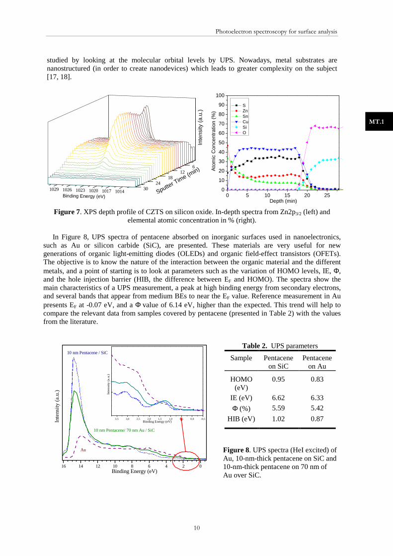
3.3. Chemical characterization of new chalcogenide absorbers for next generation photovoltaic technologies (PV): in-depth XPS concentration profiles Cu2ZnSnS4 and Cu2ZnSnSe4 (CZT(S,Se)) compounds are receiving an increasing interest for the replacement of chalcopyrite absorbers used in Cu(In,Ga)(S,Se)2 (CIS) solar cells [14,15]. In relation to CIS based PV technologies, CZT(S,Se) materials are formed by abundant and non-toxic materials, which make them more suited for their massive deployment in the next years to compete in a more efficient way with traditional non-renewable energy sources. However, efficiencies achieved with these absorbers are still lower than 10%. One of the reasons for low efficiency values in these devices is the potential presence of secondary phases, probably at the grain boundary regions, which deteriorate the optoelectronic properties of the layers. Full identification and characterization of phase inhomogeneities is crucial for further optimization of these technologies In-depth XPS analysis provides both the atomic concentration profile and the chemical information of the layers when minimizing the damage produced by the Ar+ sputtering.
On the left of Figure 7, all the spectra of Zn2p3/2 orbital level from the surface to the bulk are shown. A plot like this one can be obtained from one orbital level of each element present at the sample. Using the RSF method, the atomic concentration percentage versus sputter time is calculated (on the right). The percentages of the different elements do not agree with the theoretical assumptions of composition of the material. The Cu signal is large enough all along the layer which indicates that some Cu-rich secondary phases (like Cu3SnS4) are also formed. This phase will certainly alter the electric behaviour of the solar cell. The comparison of XPS in-depth data with X-ray diffraction (XRD) and Raman scattering spectroscopy data will help in clarifying this point [16].
3.4. Study of VB and molecular bonds: determination of HOMO levels in pentacene deposited on nanostructured substrates Organics electronics, i.e. the conjunction between organic surfaces and inorganic materials, is one of the most outstanding fields in material science. Correct understanding of these systems requires knowledge of the physics and chemistry of its surfaces and interfaces. The complex structures created by the chemical reactions between organic adsorbed molecules and metal surfaces can be
92 90 88 86 84 82 80 78
In
tens
ity (
a.u.
)
408 406 404 402 400 398 396 394
170 168 166 164 162 160 158 156
Binding Energy (eV)
Photoelectron spectroscopy for surface analysis
10
MT.1
studied by looking at the molecular orbital levels by UPS. Nowadays, metal substrates are nanostructured (in order to create nanodevices) which leads to greater complexity on the subject [17, 18].
Figure 7. XPS depth profile of CZTS on silicon oxide. In-depth spectra from Zn2p3/2 (left) and elemental atomic concentration in % (right).
In Figure 8, UPS spectra of pentacene absorbed on inorganic surfaces used in nanoelectronics,
such as Au or silicon carbide (SiC), are presented. These materials are very useful for new generations of organic light-emitting diodes (OLEDs) and organic field-effect transistors (OFETs). The objective is to know the nature of the interaction between the organic material and the different metals, and a point of starting is to look at parameters such as the variation of HOMO levels, IE, Φ, and the hole injection barrier (HIB, the difference between EF and HOMO). The spectra show the main characteristics of a UPS measurement, a peak at high binding energy from secondary electrons, and several bands that appear from medium BEs to near the EF value. Reference measurement in Aupresents EF at -0.07 eV, and a Φ value of 6.14 eV, higher than the expected. This trend will help to compare the relevant data from samples covered by pentacene (presented in Table 2) with the values from the literature.
Table 2. UPS parameters Sample Pentacene
on SiC Pentacene
on Au HOMO
(eV) 0.95 0.83
IE (eV) 6.62 6.33
Φ (%) 5.59 5.42
HIB (eV) 1.02 0.87
Figure 8. UPS spectra (HeI excited) of Au, 10-nm-thick pentacene on SiC and 10-nm-thick pentacene on 70 nm of Au over SiC.
1029 1026 1023 1020 1017 1014
612
1824
30Sputter T
ime (min)
Inte
nsity
(a.
u.)
Binding Energy (eV) 0 5 10 15 20 250
10
20
30
40
50
60
70
80
90
100
Ato
mic
Con
cent
ratio
n (%
)
Depth (min)
S Zn Sn Cu Si O
16 14 12 10 8 6 4 2 0
3,5 3,0 2,5 2,0 1,5 1,0 0,5 0,0 -0,5
In
ten
sity
(a
.u.)
Binding Energy (eV)
Au
Inte
nsity
(a.
u.)
Binding Energy (eV)
10 nm Pentacene/ 70 nm Au / SiC
10 nm Pentacene / SiC

Photoelectron spectroscopy for surface analysis
11
MT.1
AAAAcknowledgmentscknowledgmentscknowledgmentscknowledgments
The authors would like to thank Dr. David Amabilino and Angela Bejarano for allowing to use unpublished results of ARXPS, and Johanna Fuks for the work done in UPS with us in the past.
ReferencesReferencesReferencesReferences
[1] A. Einstein was awarded the Nobel in 1921 for his developments on the photoelectric theory. [2] K. M. Siegbahn was awarded the Nobel in 1981 for his achievements in XPS. [3] W. Heisenberg was awarded the Nobel in 1932 for his contributions in quantum mechanics. [4] M. P. Seah, D. Briggs 1992 Practical Surface Analysis by Auger and X-ray Photoelectron
Spectroscopy, Wiley & Sons Chichester, UK. [5] D. Cahen, A. Kahn 2003 Advanced Materials 15 271. [6] Multipak V8.2B, 2006 ULVAC-PHI Inc. and CasaXPS V2.3.15, 2009 Casa Software Ltd. [7] S. Tougaard 1998 Surface and Interface Analysis 26 249. [8] P. J. Cumpson 1995 Journal of Electron Spectroscopy and Related Phenomena 73 25. [9] C. Serre, L. Calvo-Barrio, A. Perez-Rodriguez et al 1996 Journal of Applied Physics 79
6907. [10] Detailed information about these instruments in www.phi.com and www.specs.com. [11] D. R. Baer, M. H. Engelhard 2010 Journal of Electron Spectroscopy and Related
Phenomena 178-179 415. [12] R. López, R. Gómez, S. Oros-Ruiz 2011 Catalysis Today, article in press. [13] J.J. Dubowski, O. Voznyy, G. M. Marshall 2010 Applied Surface Science 256 5714. [14] L. Calvo-Barrio, A. Perez-Rodriguez et al 2001 Vacuum 63 315. [15] X. Fontane, V. Izquierdo-Roca, L. Calvo-Barrio et al 2009 Applied Physics Letters 95
261912. [16] X. Fontane, L. Calvo-Barrio et al 2011 Applied Physics Letters 98 181905. [17] N. Kock 2008 Journal of Physics: Condensed Matter 20 184008. [18] F. Amy, C.Chan, A.Kahn 2005 Organic Electronics 6 85.