phase lock - diyguitarpedals.com.au
TRANSCRIPT

1www.diyguitarpedals.com.au
Phase Lock Design By Erik Vincent
Do you have a phaser in your arsenal? The Phase Lock is based on The MXR Phase 90, a classic phaser with a natural sounding swell, a timeless analogue phaser. The Phase Lock also shares that one speed control. That 1 knob has an impressive range, from subtle to swoosh, warm and shimmery. Add some chorus and/or delay and get ready to head for outer space. This will fit inside a 1590B enclosure or larger.

2www.diyguitarpedals.com.au
Bill of Materials, Phase Lock Capacitor Resistor
C1 10nF (film) R1 470KC2 47nF (film) R2 10KC3 47nF (film) R3 470KC4 47nF (film) R4 10KC5 47nF (film) R5 10KC6 47nF (film) R6 22KC7 10μF (Electrolytic) R7 22KC8 47nF (film) R8 10KC9 10nF (film) R9 10KC10 10μF (Electrolytic) R10 10K R11 22K
Diode R12 10KD1 1N4001 R13 10KD2 1N5231 (or any other 5.1V Zener) R14 10K
R15 22KTransistors and JFETs R16 150K
Q1 2N5457 (GSD Pinout) R17 150KQ2 2N5457 (GSD Pinout) R18 56KQ3 2N5457 (GSD Pinout) R19 150KQ4 2N5457 (GSD Pinout) R20 10KQ5 2N3906 (PNP) R21 3.9M R22 1M
ICs R23 4.7KU1 TL072 R24 150KU2 TL072 R25 470KU2 TL072 R26 150K R27 150K R28 22K Potentiometer Speed 500kc (16mm) VR2 250k (trim pot)

3www.diyguitarpedals.com.au
PCB Spacing The Phase Lock PCB is spaced for 1590B sized enclosures or larger Pot Spacing The Phase Lock PCB mounted potentiometers are spaced for Alpha 16mm potentiometers without dust covers

4www.diyguitarpedals.com.au
Assembly. 1. Soldering Order. When soldering things to the PCB, the idea is to solder things on from lowest profile to tallest.
For the Phase Lock, the best order would be: resistors, diodes, trim pots, IC sockets (if socketing), transistor/FETs, ICs (if not socketing), film capacitors, electrolytic capacitors, wiring, and then potentiometers.
1.1 Resistors. Resistors are small passive components designed to create a resistance of passage of an electric current.
For this pedal we will be using 1/4 Watt resistors. These can either be 5% tolerance carbon resistors, or 1% tolerance metal film resistors. Orientation of “which way is up” doesn’t matter, so you can install them either way. After installation and soldering, do not forget to clip the remaining legs from the PCB.

5www.diyguitarpedals.com.au
1.2 Diodes. Diodes are semiconductor components typically designed to allow the flow electric current to go in one direction only.
The orientation of a diode does matter based on the cathode and anode of the diode in the circuit. Make sure the stripe on the diode lines up with the stripe on the PCB’s silkscreen. After installation and soldering, do not forget to clip the remaining legs from the PCB.
1.3 Trim Potentiometers These are small variable resistors, but unlike regular size potentiometers, are not designed for constant adjustments, but rather fixed adjustments.
These devices have holes on the PCB that will allow them to only be soldered in one way.
6www.diyguitarpedals.com.au
1.4 IC Sockets. These are holders that allow easy installation and uninstallation of ICs.
These devices will have a silk screen notch to indicate an orientation with the IC or socket for the IC. Just make sure the IC notches match.
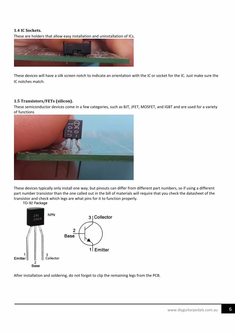
1.5 Transistors/FETs (silicon). These semiconductor devices come in a few categories, such as BJT, JFET, MOSFET, and IGBT and are used for a variety of functions
These devices typically only install one way, but pinouts can differ from different part numbers, so if using a different part number transistor than the one called out in the bill of materials will require that you check the datasheet of the transistor and check which legs are what pins for it to function properly.
After installation and soldering, do not forget to clip the remaining legs from the PCB.

7www.diyguitarpedals.com.au
1.6 Integrated Circuits. Also known as ICs, these are small analog or digital components that provide specific electrical functions.
Orientation of “which way is up” will be indicated by a notch on the silkscreen on the PCB and a dot or bar on the actual IC itself. Do make sure they match.
1.7 Capacitors (film). Film capacitors are small passive components designed to hold a small amount of charge in a circuit.
Orientation of “which way is up” doesn’t matter, so you can install them either way. After installation and soldering, do not forget to clip the remaining legs from the PCB.
1.8 Capacitors (electrolytic). Electrolytic capacitors are small passive components designed to hold a small amount of charge in a circuit.
Electrolytic capacitors are typically polarized, so orientation will matter.

8www.diyguitarpedals.com.au
After installation and soldering, do not forget to clip the remaining legs from the PCB.
1.9 Wiring. Wires used for the pedal are for delivering power over the hot and ground wires as well as signal for the input and output.
These can be installed at the very end, but in some situations, installing them before potentiometers are soldered in

9www.diyguitarpedals.com.au
place can be advantageous. Colored wire doesn’t change the properties, but using color codes for hot and ground wires, like red being hot, and black being ground, are common place. Typically, stranded hook-up wire, AWG 24 or 22 is used for this task. Using wire strippers, strip away about 1/8” (3mm) of the wire from either end and then using a soldering iron, tin the exposed tips with solder before installing into the PCB.
1.10 Potentiometers. Potentiometers are variable resistors that are used for controlling aspects of the pedal.
This pedal can utilize 16mm pots. These are typically installed on the backside of the PCB and uses the included washer and jam-nut to mechanically secure the PCB to the enclosure via a strategically drilled hole on the enclosure. Orientation of potentiometer is preferred to line up the knob on the silk screen with the knob of the potentiometer.

10www.diyguitarpedals.com.au
1.11 Off Board Wiring Diagram. Potentiometers are variable resistors that are used for controlling aspects of the pedal. Using a non-switched miniature DC Jack and 2 Mono Jacks

11www.diyguitarpedals.com.au

12www.diyguitarpedals.com.au
Phase Lock Circuit Analysis for modifying purposes. 2. Phase Lock Circuit. The Phase Lock schematic can be broken down into some simpler blocks: Power Supply, Input Buffer, Phase Shifting Stage, LFO, and Output Buffer.
The circuit is designed around a Phase Shifting Stage with an Input Buffer to avoid tone sucking. The last Output Buffer Stage will mix the wet and dry signal in order to create the signal cancellation. The LFO creates the sub-sonic carrier signal that modulates the notches, shifting them among the frequency band.
This modulation is controlled by one knob which set the speed of the effect (frequency of the LFO).
The input impedance on the Blues Crusher is close to 245K Ω, allowing the pedal to not overload the pickups on the guitar or to tone suck, but as a rule of thumb, increasing to 1M would be ideal.

13www.diyguitarpedals.com.au
3. Power Supply. The Power Supply Stage provides the electrical power and bias voltage to all the circuitry, the whole power consumption is low and estimated around 5mA:
• The Zener diode D2 is decoupled to ground with a 10uF electrolytic capacitor C7, removing all ripple from the supply line. The 5.1 voltage reference will be also used as a virtual ground in all op-amp stages.
• Capacitor C8 between supplies also removes noise from the power lines. • The diode D1 protects the pedal against reverse polarity connections.

14www.diyguitarpedals.com.au
4. Input Buffer. The Input Buffer Stage is a buffer op-amp with unitary gain placed to keep high input impedance and avoid tone sucking. It also filters the input humming harmonics with an RC network.
• R1 is an anti-pop resistor. • The 0.01uF cap C1 cap blocks DC and provides simple high pass filtering with R3. (larger values let more bass into
the circuit) Humming frequencies below 33Hz will be attenuated, the cut-off frequency can be calculated as: fc = 1 / (2πRC) fc = 1 / (2π⋅R3⋅C1) fc = 1 / (2π⋅470,000 ⋅ 0.000000010) = 33.86 Hz
• The big 470K resistor R3 will bias the input to virtual ground (+Vref = 5.1V).

15www.diyguitarpedals.com.au
4.1 Input Impedance. The input impedance is defined by the formula: Zin = R2 + (R1 Parallel to R3 Parallel to Zin2op-amp) If you look up the datasheet for the TL072, under the electrical characteristics, the input resistance is 1012.
Zin = 10K + 235K Zin = 245,000Ω
Therefore, the Phase Lock input resistance is 245K, which isn’t bad, but the closer to 1M it is, the better. Increasing R1 and R3 to 2.2M would bring the input resistance up to 1.1M, although that would also effect the input high pass filter.

16www.diyguitarpedals.com.au
5. Phase Shift Stage. The Phase Shifting Stage is the core of the circuit. It is based on the repetition of the Elementary Shifting Unit. Each of this units will shift the phase of the original signal up to 90°.

17www.diyguitarpedals.com.au
5.1 The Elementary Shifting Unit It is an RC network fed by a signal V1 at the Capacitor input, and by V2 (V1 inverted or V2 shifted 180°) at the Resistor input.
The circuit can be studied as a high pass - low pass filter:
• With V1=source and V2=GND, the shifting RC network is a standard passive high pass filter. With the typical frequency response: fc = 1 / (2πRC) and phase response: Φ = arc tan (1/2πfRC)
• With V2=source and V1=GND, the shifting RC network is a standard passive low pass filter. With the typical frequency response: fc = 1 / (2πRC) and phase response: Φ = -1 ⋅ arc tan (2πfRC)

18www.diyguitarpedals.com.au
Using superposition the RC circuit is analyzed in 3 steps:
1. Apply V1 and make V2=GND. 2. Apply V2 and make V1=GND. 3. Calculate the response as a sum of the results caused by each independent V1 and V2 sources acting alone. So
the output is the sum of step1 + step2.
In the image below the amplitude and phase (Bode Plot) of each step of the superposition analysis are shown. For this example, C=47nF and R=24K with fc=141Hz are used.
The blue amplitude trace of the total response is constant (step 3), there is no signal attenuation. The red phase trace at the cut-off frequency is defined as the frequency point where the capacitive reactance and resistance are equal R = XC, the phase shift is 90° following the formula:
Φ / 2 = tan-1 (2πfRC)
f = (tan (Φ / 2)) / (2πRC)
The phase at frequency cut-off is not 45° as in a standard passive RC filter but doubled to 90°.

19www.diyguitarpedals.com.au
Stringing up two of this RC networks in series, the phase at fphaser will be shifted up to 90°+90°=180° degrees. If the processed signal (with 180° phase-shift) is added to the original one, the result will be a signal with amplitude cancellation only at fphaser creating a notch at this freq.
Therefore, adding series pairs of Phase Shifting Units will create more notches: 2 stages = 1 notch, 4 stages = 2 notches and so on. The effect is enhanced if the notches move up and down in frequency, the easiest way is by changing the resistor value of the RC chain.

20www.diyguitarpedals.com.au
5.2 Phase Lock Shifting Unit Using the Elementary Shifting Unit concept, the Phase 90 uses an inverting operational amplifier with the RC shifter at the (+) input. In the image below the circuit is presented with the signals at the key points. The phase shift of 90° will take place at the fphaser = fcut-off of the RC network.
• The Blue waveform Vin is the input signal, for the example a unitary signal is used (module 1, phase 0°). • The Green waveform VX is the signal at (-) or (+) op-amp inputs. Taking the RC as a standard high pass filter,
because +Vref is virtual ground and can be considered as GND point. The fcut-off =1/(2πRC) with a 45° phase and the amplitude is Vin-3dB or in other words 1/√2 (that is why the green waveform is smaller than the blue and the red).
• The Red waveform Vout is the output signal, module 1 and phase +90°.
The mathematics behind the waveforms can be calculated using complex numbers; in an inverting op-amp topology, the output voltage cal be calulated as:
Vout = -R ((Vin – Vx) / R) – Vx = -Vin + 2Vx Where:
• Vin is module 1 phase 0° or in complex expression: 1cos(0°) + 1sen(0°)j = 1 • VX is module 1/√2 phase 45° or in complex expression:1/√2cos(45°) + 1/√2sen(45°)j = 0.5 + 0.5j
Vout=−Vin+2VX=−1+2(0.5+0.5j)=jVout=−Vin+2VX=−1+2(0.5+0.5j)=j
Vout = -Vin + 2Vx = -1 + 2(0.5 + 0.5j) = j
The output is j which means module 1 and 90° phase.

21www.diyguitarpedals.com.au
5.3 How to move the notches The Phasing guitar effect is accomplished when the notches are shifted up and down in the audio band automatically. This variation is done by modifying the value of R at (+), there are several approaches to do so:
• The early method used in Magnatone Vibrato was to use Varistors (variable resistance depending on the voltage placed across it) not very sensitive and need to be driven by high voltage signals over 20V.
• The OTA Operational Transconductance Amplifier used in EHX Small Stone and Maestro Stage Phaser is an over-complex solution compared to the other solutions.
• The LDR Light Dependent Resistor used on MXR Phase-100 and Univibe is linear and easy to use. • MXR Phase90 uses a FET as a variable resistor placed in parallel with R. As it will be seen in the next point, the
variable resistor value is proportional to the LFO voltage at the FET gate:

22www.diyguitarpedals.com.au
5.4 Using a FET as a Variable Resistor / 2N5457 Matching for Phase Lock: A 2N5457 N-Channel FET transistor can be used as a Voltage Controlled Resistor where the resistance value between the Drain and Source terminals (rDS) is controlled by the Gate voltage.
The I-V characteristic graph shows that in Linear Region, the drain-source resistance is controlled only by the gate-source voltage:
• If VGS=0: rDS is minimum (rDS=VDS/IDS). It goes to the saturation region.
• If VGS is increased (negatively for n-channel) : rDS value raise.
• If VGS= VGS cut-off or VGS pinch-off : rDS is maximum. It goes to Channel off region.
The VGS cut-off voltages differ from one FET to another from the same manufacturer. The pinch-off occurs at a particular reverse bias (VGS) of the gate-source junction. Due to foundry limitations, it is much harder to make consistent JFETs than to make consistent bipolar devices. The 2N5457 is guaranteed to cut-off completely between -1.3 and -3.5, it is a big margin, making the voltage range to control the FET different between transistors in the same circuit.
The best performance in the Phase 90 is when:
1. All the FETs move together: They should have similar cut-off voltage, with a similar curve and rDS to a given VGS. The best way to achieve it is to match the FETs.
2. The rDS sweeps over a wide range of resistance values, so the notches can be shifted around fairly. The VGS cut-
off should be as big as possible giving a wider LFO sweep span.
With these premises and assuming that a 5.1V zener is being used (VG=5.1V), the right biasing of the FET should make the VGS to vary from 0 to VGS cut-off.
• To make VGS = 0, VS = VZENER = 5.1V and VG = 5.1V. • To make VGS = VGS cut-off, VS = VZENER = 5.1V and VG = 5.1V + Vcut-off, depending on the FET Vcut-off is -1.3 to -3.5V, so
VG=3.8 to 1.6V. The safer way is to adjust it close to 3.8 Volts, and the transistor will go to Channel Off region for sure.
The triangular wave generated by the LFO is applied to VG and must be aligned with this bias point using the 250K Rtrimmer.
The rDS values are normally between some hundred ohms to some mega ohms. The 22K resistor parallel with the FET will result in a combined resistance smaller than 22K, i.e : (22KΩ // 100Ω)=100Ω and (22KΩ // 2MΩ)= 22KΩ.

23www.diyguitarpedals.com.au
5.5 Phase Lock Notches Frequency: The Phase Lock is based on 4 phase shifting units, creating 2 notches. In order to generate a 180° shifted output, the phase shift is distributed like:
There are two possible ways to reach the 180 desired output with 1/4 increments (this is why there are two notches):
• Doing 180° / 4 = 45° increments: 45° - 90° - 135° - 180°. • Adding 360° and doing the same operation (180° + 360°) / 4 = 135° increments: 135° - 270° - 405° - 540°. (540°
and 180° have the same phase characteristics).
The frequency where these notches are placed is calculated using the main formula:
f = (tan (Φ / 2)) / (2πRC)
Where Φ is the desired phase in each increment (45° or 135°), R=22K and C=47nF.
fnotch1 = (tan (45 / 2)) / (2π ⋅ 22,000 ⋅ 0.000000047) = 63.756 Hz
fnotch1 = (tan (135 / 2)) / (2π ⋅ 22,000 ⋅ 0.000000047) = 371.6 Hz
The frequency response of the Phase Lock, with notches at 63Hz and 371Hz:

24www.diyguitarpedals.com.au
5.6 Phase Lock Feedback Resistor: The feedback resistor labeled R28 makes the effect stronger and more pronounced, causing boost and even distortion in the midrange. Not populating the feedback resistor makes the Phase Lock more balanced and smooth.
The output signal has two notches where the original and the phased signal have 180 phase difference, creating signal cancellation. At the same time, other frequencies will get the opposite effect, being reinforced when the input and phased waveforms have 0 or 360 phase difference. Having it feedback part of the output signal into the Shifting Stage chain will reinforce keeping the cancellation points.
In the graph above the frequency response with (blue) and without (red) R28 is shown. Adding the feedback resistor creates a mid-hump and additional gain.

25www.diyguitarpedals.com.au
The feedback can be routed to different phase stage, each stage has a singular phase difference, so the peaks generated have a different voice to each stage. Find below the result of routing back the R28 from the output to the 1st, 2nd (default in Phase Lock), 3rd and 4th stage. Each case will result in a different tone response (red trace shows response without R28 and blue trace with R28):

26www.diyguitarpedals.com.au
6. Low-Frequency Oscillator The Low-Frequency Oscillator generates a triangular sub-audio waveform. The signal will command the phase shifting operation by changing the VG of the FET transistors and therefore the source-drain resistance.
The LFO design is based in a Schmitt Trigger - Integrator modified topology. The cap C9 ramps up and down at a rate which depends on the current going into/out of it as controlled by the VR1 Speed potentiometer.
The output of the op-amp creates a square waveform while at the "OUT" point is the triangular LFO signal. The signal can be trimmed from tenths of Hz to some Hertz as shown below:
27www.diyguitarpedals.com.au
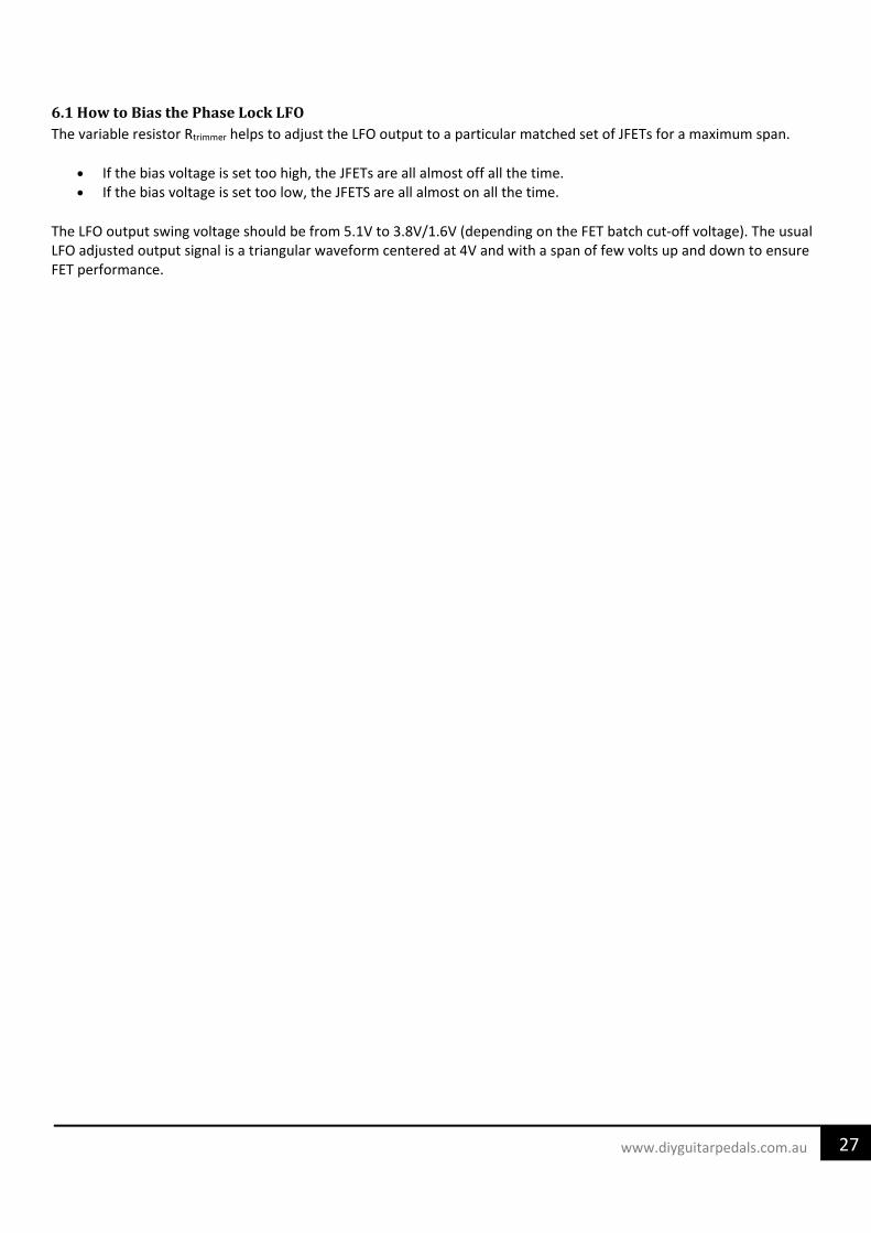
6.1 How to Bias the Phase Lock LFO The variable resistor Rtrimmer helps to adjust the LFO output to a particular matched set of JFETs for a maximum span.
• If the bias voltage is set too high, the JFETs are all almost off all the time. • If the bias voltage is set too low, the JFETS are all almost on all the time.
The LFO output swing voltage should be from 5.1V to 3.8V/1.6V (depending on the FET batch cut-off voltage). The usual LFO adjusted output signal is a triangular waveform centered at 4V and with a span of few volts up and down to ensure FET performance.

28www.diyguitarpedals.com.au
7. Output Buffer. The Output Buffer Stage mixes the wet and dry signals generating the moving-frequency-notches output. The capacitor C2 also provides additional signal filtering.
This last stage is a PNP Common Emitter Amplifier. Both signals are applied through the base of Q5, the ratio of R16 (DRY Signal) and R17 (WET Signal) indicates that the original and processed signals are mixed at 50% as they are both the same value.
• After the transistor amplifier, there is a high pass RC network formed by C6, R19. The cut-off frequency is 22 Hz (1 / (2π x R19 x C6), removing humming and DC component from the output and also protecting the circuit against high current loads.
• Any other PNP transistor like 2N4125, 2N4250, 2N5087 with gain over 200 can replace the 2N3906.
• The output impedance provided by this circuit is around 3.4K

29www.diyguitarpedals.com.au
8. Voltage Readouts. Below are the voltage readouts of the ICs onboard, assuming 9V Power Supply.
IC and FET read-outs
KNOBS
- SPEED: ALL THE WAY COUNTER CLOCKWISE

30www.diyguitarpedals.com.au
9. JFET Matching Thanks to RG Keen for providing the design for a good JFET Match Tester.
If this were to be bread-boarded, the Q1 is the JFET that will be tested in this circuit.
The 10K resistor, R3, sets the matching current by taking the 4.5V bias over itself (4.5V / 10K)
Getting the voltages between the 4.5V and the gate of the JFET (Data Point 1, D1) will give you the VGS. The goal is to try and get a set that the furthest two apart are no more than 100mV apart. So, a group that is 2.48V, 2.44V, 2.53V, and 2.52V would be good as the furthest apart in this group are 2.44V and 2.53V, being only 90mV apart from each other. If one of these were in the 1.xxx volt range, that one would likely be too far out to use.

31www.diyguitarpedals.com.au
10. Modifications Following is a couple of worthwhile modifications that can be applied to the Phase Lock. 10.1 Capacitors If you change the values of C2 and C3 from 47nF to 15nF on C2 and 220nF on C3, this will create a similar sound to a UniVibe (especially if you do not populate R28 and R16).
10.2 Resistors Not populating the R28 feedback resistor makes the Phase Lock more balanced and smooth. Not populating R16 will stop the dry signal from coming in. This will give a more vibrato output. The Phase Lock has a set output level, which is determined by R27. To reduce gain, decrease to 120K. To increase gain, increase to 180K.

32www.diyguitarpedals.com.au
11. Schematic

5/26/2021 6:48 AM C:\Users\evincent\Documents\eagle\_Pedals\Phase Lock\Phase Lock 1590B Enclosure.brd
INOUT
STOMP
LED
POWER
SPEED

5/26/2021 6:53 AM C:\Users\evincent\Documents\eagle\_Pedals\Phase Lock\Phase Lock 125B Enclosure.brd
STOMPLED
POWER
INOUT
SPEED

10/12/2019 10:14 AM C:\Users\evincent\Documents\eagle\_Pedals\Phase Lock\Phase Lock Layout.brd
SPEE
D
43.2
52.1
25.3
26.0
7.2