pfc regulator
TRANSCRIPT
Comprehensive information online to read the original online store Downloads DATASHEETTechnology Forum Business Channel
Embedded System Single Chip DSP EDA / PLD interface circuit storage displayOptoelectronics PowerSensing / control analog communications network wireless communications Meter ConsumerElectronics Automotive
Position: Home → Technical articles → Power → body
S3C6410 ARM11 development board +4.3TFT 2,400 yuan OMAP3530: DevKit8000 Assessment
Board
EM-AT91SAM3U development board 750 yuan LPC1766 development board
EM STM3210E D l t B dAverage current method of application of control chip UC3854BN
Release date :2006-04-28 Of: Professor Yeung Source: Power Technology
Abstract: the average current method and thecharacteristics of peak current control method, and adetailed analysis of the average current method ofapplication of control chip UC3854BN Finally, theexperimental waveforms are provided.Keywords: average current control; peak currentcontrol; power factor correction; slope compensation;harmonic oscillation
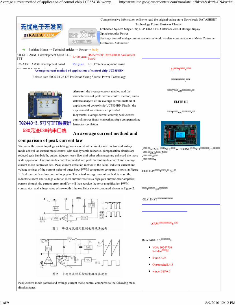
An average current method andcomparison of peak current lawWe know the circuit topology switching power circuit into current mode control and voltagemode control, as current mode control with fast dynamic response, compensation circuits arereduced gain bandwidth, output inductor, easy flow and other advantages are achieved the morewide application. Current mode control is divided into peak current mode control and averagecurrent mode control of two. Peak current detection method is the actual inductor current andvoltage settings of the current value of outer input PWM comparator compares, shown in Figure1. Peak current law, low current loop gain. The actual average current method is to set theinductor current and voltage outer an ideal current receives a high-gain current error amplifier,current through the current error amplifier will then receive the error amplification PWMcomparator, and a large value of sawtooth ( the oscillator slope) compared shown in Figure 2.
Peak current mode control and average current mode control compared to the following maindisadvantages:
51 Ƭ
Ƭ ѧϰ
ELITE-III
Ƭ ѧϰ
- ATMEL STC WINBOND SST оƬ- USB ڱ- ǿ- װ
ELITE-IV Ƭ 248
Ƭ дU
-SL811HST
ARM
Basic2410+3.5 װ
VGA 1024*768S-video
linux2.6.28
Qtextended4.4.3
wince BSP6.0
Average current method of application of control chip UC3854BN worry ... http://translate.googleusercontent.com/translate_c?hl=en&sl=zh-CN&u=htt...
1 of 9 8/9/2010 12:12 PM
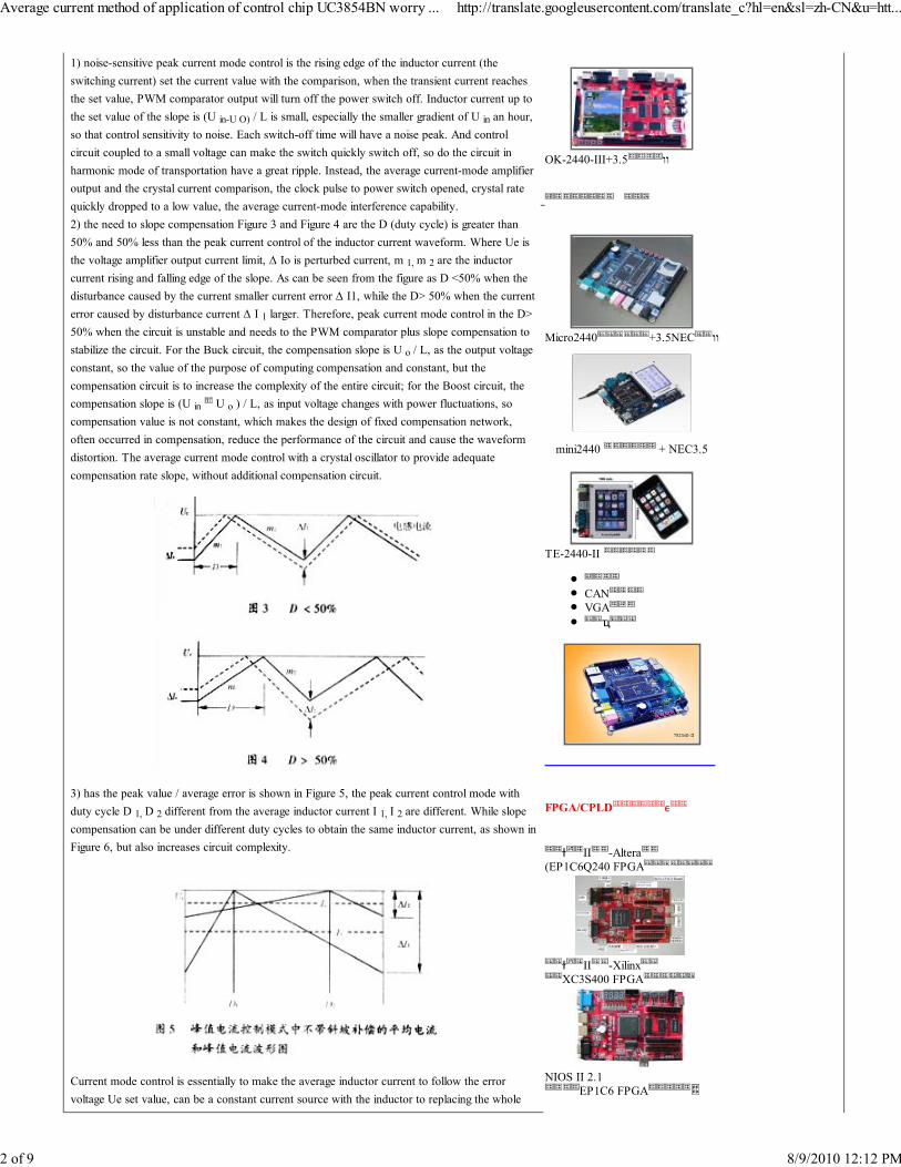
1) noise-sensitive peak current mode control is the rising edge of the inductor current (theswitching current) set the current value with the comparison, when the transient current reachesthe set value, PWM comparator output will turn off the power switch off. Inductor current up tothe set value of the slope is (U in-U O) / L is small, especially the smaller gradient of U in an hour,so that control sensitivity to noise. Each switch-off time will have a noise peak. And controlcircuit coupled to a small voltage can make the switch quickly switch off, so do the circuit inharmonic mode of transportation have a great ripple. Instead, the average current-mode amplifieroutput and the crystal current comparison, the clock pulse to power switch opened, crystal ratequickly dropped to a low value, the average current-mode interference capability.2) the need to slope compensation Figure 3 and Figure 4 are the D (duty cycle) is greater than50% and 50% less than the peak current control of the inductor current waveform. Where Ue isthe voltage amplifier output current limit, Δ Io is perturbed current, m 1, m 2 are the inductorcurrent rising and falling edge of the slope. As can be seen from the figure as D <50% when thedisturbance caused by the current smaller current error Δ I1, while the D> 50% when the currenterror caused by disturbance current Δ I 1 larger. Therefore, peak current mode control in the D>50% when the circuit is unstable and needs to the PWM comparator plus slope compensation tostabilize the circuit. For the Buck circuit, the compensation slope is U o / L, as the output voltageconstant, so the value of the purpose of computing compensation and constant, but thecompensation circuit is to increase the complexity of the entire circuit; for the Boost circuit, thecompensation slope is (U in U o ) / L, as input voltage changes with power fluctuations, socompensation value is not constant, which makes the design of fixed compensation network,often occurred in compensation, reduce the performance of the circuit and cause the waveformdistortion. The average current mode control with a crystal oscillator to provide adequatecompensation rate slope, without additional compensation circuit.
3) has the peak value / average error is shown in Figure 5, the peak current control mode withduty cycle D 1, D 2 different from the average inductor current I 1, I 2 are different. While slopecompensation can be under different duty cycles to obtain the same inductor current, as shown inFigure 6, but also increases circuit complexity.
Current mode control is essentially to make the average inductor current to follow the errorvoltage Ue set value, can be a constant current source with the inductor to replacing the whole
OK-2440-III+3.5 װ
Micro2440 +3.5NEC װ
mini2440 + NEC3.5
TE-2440-II
CANVGA
ҵ
FPGA/CPLD
ɫ II -Altera(EP1C6Q240 FPGA
ɫ II -XilinxXC3S400 FPGA
NIOS II 2.1EP1C6 FPGA
Average current method of application of control chip UC3854BN worry ... http://translate.googleusercontent.com/translate_c?hl=en&sl=zh-CN&u=htt...
2 of 9 8/9/2010 12:12 PM
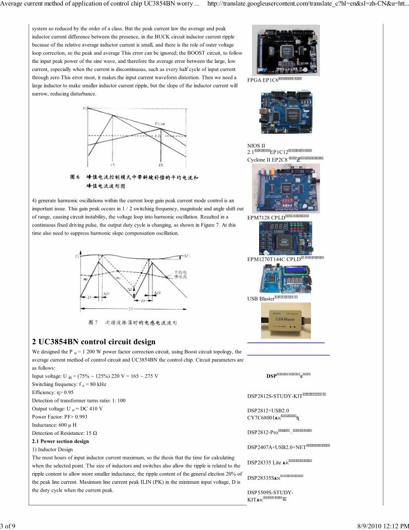
system so reduced by the order of a class. But the peak current law the average and peakinductor current difference between the presence, in the BUCK circuit inductor current ripplebecause of the relative average inductor current is small, and there is the role of outer voltageloop correction, so the peak and average This error can be ignored; the BOOST circuit, to followthe input peak power of the sine wave, and therefore the average error between the large, lowcurrent, especially when the current is discontinuous, such as every half cycle of input currentthrough zero This error most, it makes the input current waveform distortion. Then we need alarge inductor to make smaller inductor current ripple, but the slope of the inductor current willnarrow, reducing disturbance.
4) generate harmonic oscillations within the current loop gain peak current mode control is animportant issue. This gain peak occurs in 1 / 2 switching frequency, magnitude and angle shift outof range, causing circuit instability, the voltage loop into harmonic oscillation. Resulted in acontinuous fixed driving pulse, the output duty cycle is changing, as shown in Figure 7. At thistime also need to suppress harmonic slope compensation oscillation.
2 UC3854BN control circuit designWe designed the P o = 1 200 W power factor correction circuit, using Boost circuit topology, theaverage current method of control circuit and UC3854BN the control chip. Circuit parameters areas follows:Input voltage: U in = (75% ~ 125%) 220 V = 165 ~ 275 VSwitching frequency: f s = 80 kHzEfficiency: η> 0.95Detection of transformer turns ratio: 1: 100Output voltage: U o = DC 410 VPower Factor: PF> 0.993Inductance: 600 μ HDetection of Resistance: 15 Ω2.1 Power section design1) Inductor DesignThe most hours of input inductor current maximum, so the thesis that the time for calculatingwhen the selected point. The size of inductors and switches also allow the ripple is related to theripple content to allow more smaller inductance, the ripple content of the general election 20% ofthe peak line current. Maximum line current peak ILIN (PK) in the minimum input voltage, D isthe duty cycle when the current peak.
FPGA EP1C6
NIOS II2.1 EP1C12Cyclone II EP2C8 Ƶ
EPM7128 CPLD
EPM1270T144C CPLD
USB Blaster
DSP
DSP2812S-STUDY-KIT
DSP2812+USB2.0CY7C68001ѧϰ ƽ DSP2812-Pro
DSP2407A+USB2.0+NET DSP28335 Lite ѧϰ DSP28335Sѧϰ DSP5509S-STUDY-KITѧϰ
Average current method of application of control chip UC3854BN worry ... http://translate.googleusercontent.com/translate_c?hl=en&sl=zh-CN&u=htt...
3 of 9 8/9/2010 12:12 PM
2) The output capacitor selectionThe size of the output capacitor and the switching frequency ripple current, harmonic current, theoutput voltage, output ripple voltage, power and the output hold time. Capacitor current is equalto 100Hz switching frequency ripple current and harmonic currents. When considering the holdtime, the output capacitor C o is calculated by
Type in: t H - - capacitor hold time, means that the input turns off, the output voltage within acertain range of time saved, usually 15 ~ 50 μ s;
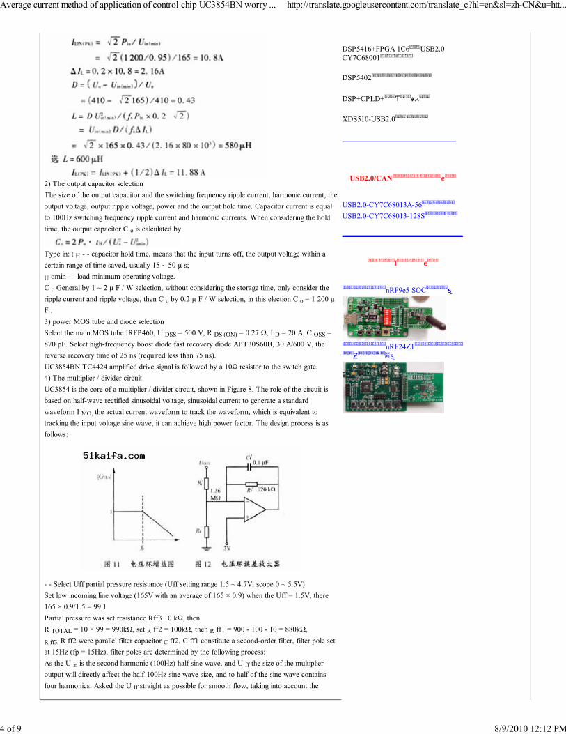
U omin - - load minimum operating voltage.C o General by 1 ~ 2 μ F / W selection, without considering the storage time, only consider theripple current and ripple voltage, then C o by 0.2 μ F / W selection, in this election C o = 1 200 μF .3) power MOS tube and diode selectionSelect the main MOS tube IRFP460, U DSS = 500 V, R DS (ON) = 0.27 Ω, I D = 20 A, C OSS =870 pF. Select high-frequency boost diode fast recovery diode APT30S60B, 30 A/600 V, thereverse recovery time of 25 ns (required less than 75 ns).UC3854BN TC4424 amplified drive signal is followed by a 10Ω resistor to the switch gate.4) The multiplier / divider circuitUC3854 is the core of a multiplier / divider circuit, shown in Figure 8. The role of the circuit isbased on half-wave rectified sinusoidal voltage, sinusoidal current to generate a standardwaveform I MO, the actual current waveform to track the waveform, which is equivalent totracking the input voltage sine wave, it can achieve high power factor. The design process is asfollows:
- - Select Uff partial pressure resistance (Uff setting range 1.5 ~ 4.7V, scope 0 ~ 5.5V)Set low incoming line voltage (165V with an average of 165 × 0.9) when the Uff = 1.5V, there165 × 0.9/1.5 = 99:1Partial pressure was set resistance Rff3 10 kΩ, thenR TOTAL = 10 × 99 = 990kΩ, set R ff2 = 100kΩ, then R ff1 = 900 - 100 - 10 = 880kΩ,
R ff3, R ff2 were parallel filter capacitor C ff2, C ff1 constitute a second-order filter, filter pole setat 15Hz (fp = 15Hz), filter poles are determined by the following process:As the U in is the second harmonic (100Hz) half sine wave, and U ff the size of the multiplieroutput will directly affect the half-100Hz sine wave size, and to half of the sine wave containsfour harmonics. Asked the U ff straight as possible for smooth flow, taking into account the
DSP5416+FPGA 1C6 USB2.0CY7C68001
DSP5402
DSP+CPLD+ Ƭ ѧϰ
XDS510-USB2.0
USB2.0/CAN
USB2.0-CY7C68013A-56USB2.0-CY7C68013-128S
ſ
nRF9e5 SOC ƽ
nRF24Z1Ƶ ƽ
Average current method of application of control chip UC3854BN worry ... http://translate.googleusercontent.com/translate_c?hl=en&sl=zh-CN&u=htt...
4 of 9 8/9/2010 12:12 PM
multiplier on the input voltage amplitude of the response speed faster, have requested that thesecond-order low-pass filter corner frequency can not be too low, and in order to maximizebandwidth asked the two poles of the same order filter frequency. When, due to U ff distortioncaused by harmonic distortion of the percentage of total harmonic distortion is limited to below1.5%, and because input electricity generated by the bridge rectifier after the 66.7% secondharmonic distortion, so that the second low-pass filter gain: 1.5% / 66.7% = 0.025Equally to the two low-pass filter gain of 0.15 per class. According to the relationship betweenthe gain and corner frequency: Gain AV = fc / fin, known input signal frequency fin = 2 × 50 =100 Hz, so corner frequency fc = 15 Hz, then calculate the size of filter capacitor
- - Calculation of resistance RM0Minimum line voltage into the I AC = 100μ A and the multiplier output is 1V, the lowestmaximum load when the incoming line voltage, UEA (voltage error amplifier output) for themaximum 6V, so according to the output multiplier formula
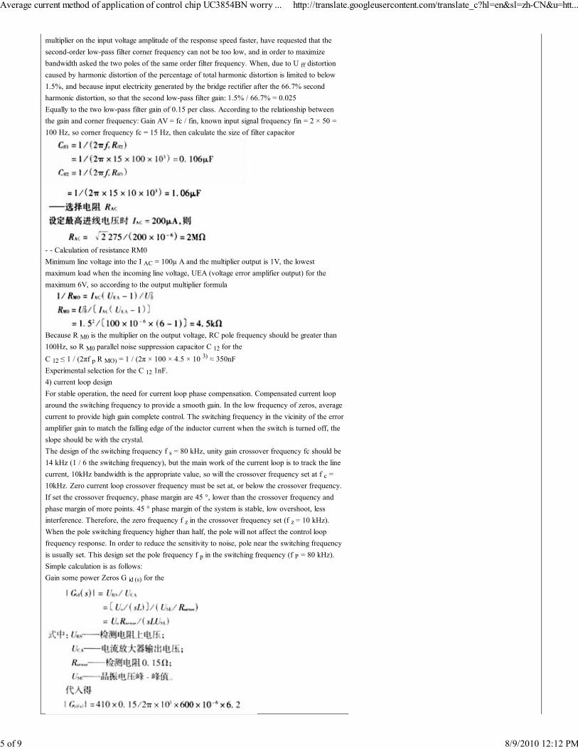
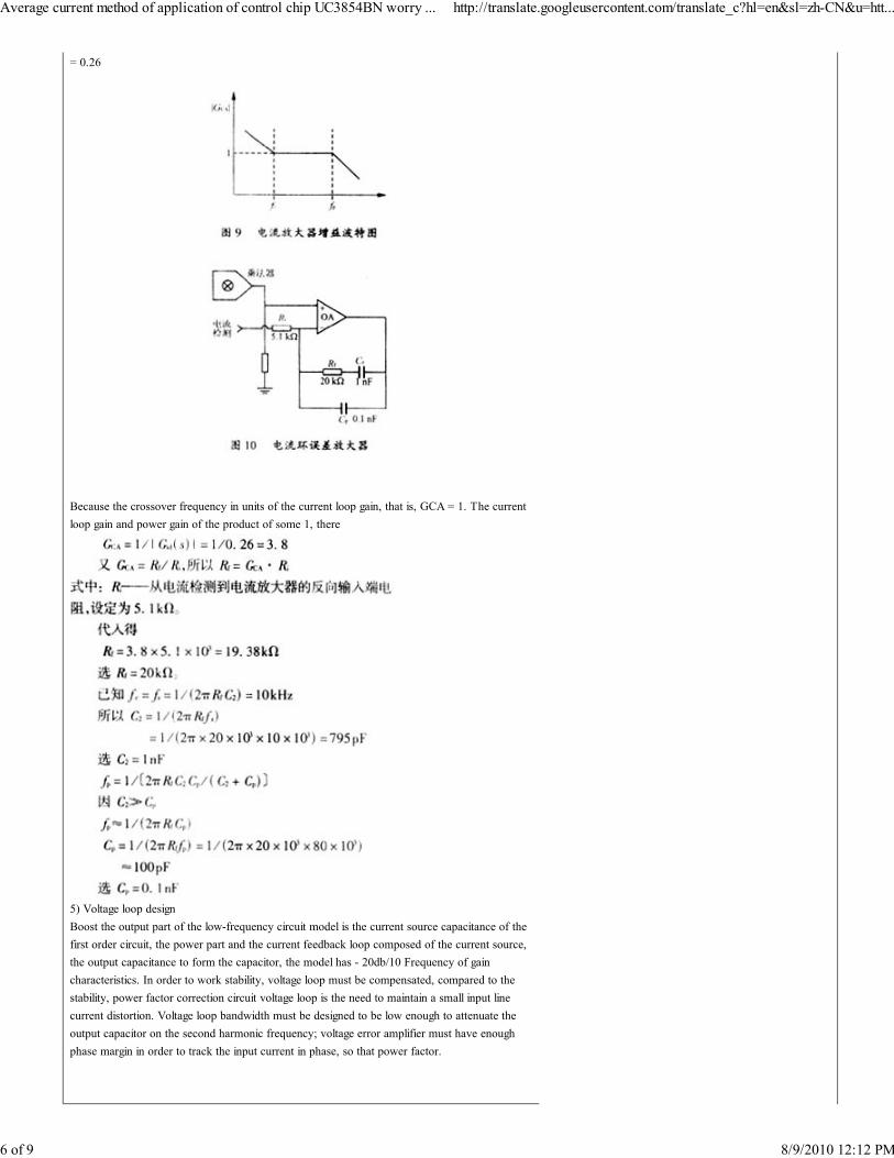
Because R M0 is the multiplier on the output voltage, RC pole frequency should be greater than100Hz, so R M0 parallel noise suppression capacitor C 12 for theC 12 ≤ 1 / (2πf p R MO) = 1 / (2π × 100 × 4.5 × 10 3) ≈ 350nFExperimental selection for the C 12 1nF.4) current loop designFor stable operation, the need for current loop phase compensation. Compensated current looparound the switching frequency to provide a smooth gain. In the low frequency of zeros, averagecurrent to provide high gain complete control. The switching frequency in the vicinity of the erroramplifier gain to match the falling edge of the inductor current when the switch is turned off, theslope should be with the crystal.The design of the switching frequency f s = 80 kHz, unity gain crossover frequency fc should be14 kHz (1 / 6 the switching frequency), but the main work of the current loop is to track the linecurrent, 10kHz bandwidth is the appropriate value, so will the crossover frequency set at f c =10kHz. Zero current loop crossover frequency must be set at, or below the crossover frequency.If set the crossover frequency, phase margin are 45 °, lower than the crossover frequency andphase margin of more points. 45 ° phase margin of the system is stable, low overshoot, lessinterference. Therefore, the zero frequency f z in the crossover frequency set (f z = 10 kHz).When the pole switching frequency higher than half, the pole will not affect the control loopfrequency response. In order to reduce the sensitivity to noise, pole near the switching frequencyis usually set. This design set the pole frequency f p in the switching frequency (f P = 80 kHz).Simple calculation is as follows:Gain some power Zeros G id (s) for the
Average current method of application of control chip UC3854BN worry ... http://translate.googleusercontent.com/translate_c?hl=en&sl=zh-CN&u=htt...
5 of 9 8/9/2010 12:12 PM
= 0.26
Because the crossover frequency in units of the current loop gain, that is, GCA = 1. The currentloop gain and power gain of the product of some 1, there
5) Voltage loop designBoost the output part of the low-frequency circuit model is the current source capacitance of thefirst order circuit, the power part and the current feedback loop composed of the current source,the output capacitance to form the capacitor, the model has - 20db/10 Frequency of gaincharacteristics. In order to work stability, voltage loop must be compensated, compared to thestability, power factor correction circuit voltage loop is the need to maintain a small input linecurrent distortion. Voltage loop bandwidth must be designed to be low enough to attenuate theoutput capacitor on the second harmonic frequency; voltage error amplifier must have enoughphase margin in order to track the input current in phase, so that power factor.
Average current method of application of control chip UC3854BN worry ... http://translate.googleusercontent.com/translate_c?hl=en&sl=zh-CN&u=htt...
6 of 9 8/9/2010 12:12 PM
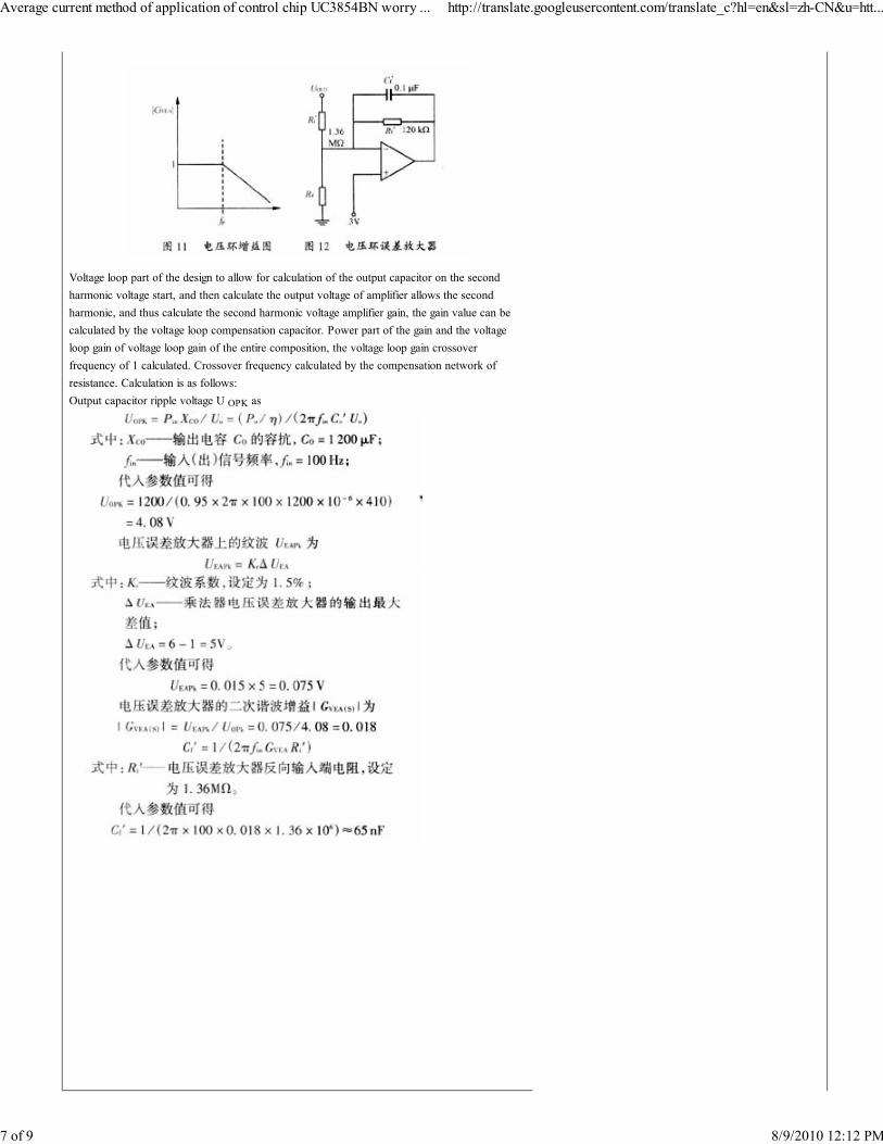
Voltage loop part of the design to allow for calculation of the output capacitor on the secondharmonic voltage start, and then calculate the output voltage of amplifier allows the secondharmonic, and thus calculate the second harmonic voltage amplifier gain, the gain value can becalculated by the voltage loop compensation capacitor. Power part of the gain and the voltageloop gain of voltage loop gain of the entire composition, the voltage loop gain crossoverfrequency of 1 calculated. Crossover frequency calculated by the compensation network ofresistance. Calculation is as follows:Output capacitor ripple voltage U OPK as
Average current method of application of control chip UC3854BN worry ... http://translate.googleusercontent.com/translate_c?hl=en&sl=zh-CN&u=htt...
7 of 9 8/9/2010 12:12 PM
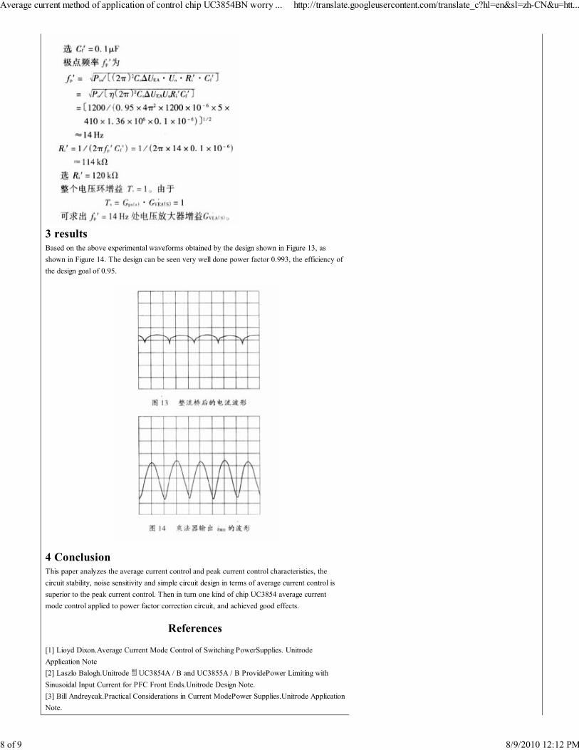
3 resultsBased on the above experimental waveforms obtained by the design shown in Figure 13, asshown in Figure 14. The design can be seen very well done power factor 0.993, the efficiency ofthe design goal of 0.95.
4 ConclusionThis paper analyzes the average current control and peak current control characteristics, thecircuit stability, noise sensitivity and simple circuit design in terms of average current control issuperior to the peak current control. Then in turn one kind of chip UC3854 average currentmode control applied to power factor correction circuit, and achieved good effects.
References
[1] Lioyd Dixon.Average Current Mode Control of Switching PowerSupplies. UnitrodeApplication Note[2] Laszlo Balogh.Unitrode UC3854A / B and UC3855A / B ProvidePower Limiting withSinusoidal Input Current for PFC Front Ends.Unitrode Design Note.[3] Bill Andreycak.Practical Considerations in Current ModePower Supplies.Unitrode ApplicationNote.
Average current method of application of control chip UC3854BN worry ... http://translate.googleusercontent.com/translate_c?hl=en&sl=zh-CN&u=htt...
8 of 9 8/9/2010 12:12 PM

[4] Modelling.Analysis and Compensation of the Current ModeConverter. Unitrode ApplicationNote.[5] Zhang Zhansong. Principle and design of switching power supply [M]. Beijing: ElectronicIndustry Press, 1998.
(End text)
News: cited in: big middle small Print Close Related Articles
Thank you, and now there is no relevant information ...
About us Links
Riviera Plaza, Futian District, Shenzhen, Hanford Garden Court 11F HenghuaTel :0755-88305872 Fax :0755-88305880
Copyright © 2005-2007 All rights reserved worry Electronic Development Network
ICP 05064233
Average current method of application of control chip UC3854BN worry ... http://translate.googleusercontent.com/translate_c?hl=en&sl=zh-CN&u=htt...
9 of 9 8/9/2010 12:12 PM