perovskite solar cells fabricated via scalable dip coating
TRANSCRIPT

Rowan University Rowan University
Rowan Digital Works Rowan Digital Works
Theses and Dissertations
5-24-2018
Perovskite solar cells fabricated via scalable dip coating methods Perovskite solar cells fabricated via scalable dip coating methods
Joseph F. Iannello Rowan University
Follow this and additional works at: https://rdw.rowan.edu/etd
Part of the Materials Science and Engineering Commons, Mechanical Engineering Commons, and the
Power and Energy Commons
Recommended Citation Recommended Citation Iannello, Joseph F., "Perovskite solar cells fabricated via scalable dip coating methods" (2018). Theses and Dissertations. 2569. https://rdw.rowan.edu/etd/2569
This Thesis is brought to you for free and open access by Rowan Digital Works. It has been accepted for inclusion in Theses and Dissertations by an authorized administrator of Rowan Digital Works. For more information, please contact [email protected].

PEROVSKITE SOLAR CELLS FABRICATED VIA SCALABLE DIP COATING
METHODS
by
Joseph F. Iannello
A Thesis
Submitted to the
Department of Mechanical Engineering
Henry M. Rowan College of Engineering
In partial fulfillment of the requirement
For the degree of
Master of Science in Mechanical Engineering
At
Rowan University
April 19, 2018
Thesis Advisor: Dr. Wei Xue, Ph.D.


iii
Acknowledgements
I would like to express my appreciation to my advisor, Dr. Wei Xue, for allowing me the
opportunity to work in his research group. This work would not have been completed
without his insightful guidance and patience for which I am deeply indebted.
I would like to thank Dr. Kandalam Ramanujachary for his continued investment in this
research project. Without which, none of this would be possible.
I would like to thank my thesis committee members, Dr. Jeffrey Hettinger and Francis
M.Haas for their help and their time that was contributed to this project.
In addition, I would like to thank Pat Jackson, Chris Kelbon, John Fogelin, and Carl Lunk
for their time and dedication spent training me on proper laboratory practices.
Lastly, I would like to thanks all of my friends and family, for their continued support
throughout the years.
iv
Abstract
Joseph Iannello
PEROVSKITE SOLAR CELLS FABRICATED VIA SCALABLE DIP COATING
METHODS
2017-2018
Wei Xue, Ph.D.
Master of Science in Mechanical Engineering
Perovskite solar cells present the possibility for less expensive electricity
generation, through the use of low cost materials and fabrication methods relative to
current silicon-based technology. Many current methods of fabricating thin film
perovskite solar cells focus on spin-coating, which inherently lacks scalability due to
particle conglomeration, poor uniformity over a larger area, and safety concerns. Dip-
coating, an alternative to spin-coating, which is explored here addresses these issues
which limit scalability. Each individual layer can be separately synthesized, deposited,
and characterized, which leads towards scalability. Choosing only the best results from
each independent layer allowed progress to the creation of a sandwich style perovskite
cell fabricated through dip coating. By using a quartz crystal microbalance, the
thicknesses of these uniform films has been determined to be in the desired range of
under one micron. Currently, there is a photo response present, with a maximum
produced voltage of 500 mV. The methods presented here create an initial starting point
for the large scale manufacturing of dip coated perovskite solar cells.

v
Table of Contents
Abstract .............................................................................................................................. iv
List of Figures ................................................................................................................... vii
Chapter 1: Introduction ....................................................................................................... 1
1.1 Motivation ................................................................................................................. 1
1.2 Background ............................................................................................................... 6
1.3 Objectives ................................................................................................................ 11
Chapter 2: Electron Transport Layer ................................................................................ 14
2.1 Zinc Oxide Nano-Rod Fabrication .......................................................................... 14
2.2 Sol-Gel Method ....................................................................................................... 16
2.3 Zinc Oxide Nanoparticles ........................................................................................ 19
2.4. Film Thickness and Purity ...................................................................................... 21
Chapter 3: Lead Iodide and Perovskite ............................................................................. 24
3.1 Lead Iodide .............................................................................................................. 24
3.2 Fabrication of Lead Iodide Films Without a Solvent .............................................. 24
3.3 Fabrication of Lead Iodide Films With a Solvent ................................................... 27
3.3.1. Spray coating. .................................................................................................. 27
3.3.2. Dip coating. ..................................................................................................... 30
3.4 Perovskite Synthesis ................................................................................................ 33
Chapter 4: Hole Transport Layer, Top Electrode and Testing .......................................... 37

vi
Table of Contents (Continued)
4.1 Spiro-MeOTAD ...................................................................................................... 37
4.2 Copper(I) Thiocyanate ............................................................................................ 39
4.3 Top Electrode .......................................................................................................... 41
4.4 Testing ..................................................................................................................... 42
Chapter 5: Conclusions and Future Works ....................................................................... 43
References ......................................................................................................................... 48

vii
List of Figures
Figure Page
Figure 1. Energy consumed globally, by type, for the year of 2017, in terawatt hours
according to the BP statistical review of world energy[1]. ............................................... 2
Figure 2. The predicted LCOE for various types of energy generation according to the
eia[2]. .................................................................................................................................. 3
Figure 3. Best research cell efficiencies from 1975 until 2017 from the National
Renewable Energy Laboratory [3]. ..................................................................................... 4
Figure 4. The method of fabricating pure silicon wafers is known as the Czochralski
process................................................................................................................................. 5
Figure 5. The general structure of a perovskite crystal. ...................................................... 7
Figure 6. The general device structure of a perovskite solar cell. ...................................... 8
Figure 7. This energy level diagram summarizes the energy level of materials used in
perovskite solar cells relative to vacuum. ........................................................................... 9
Figure 8. Current spin coating methods rely on a two-step method which involves
spinning substrates at high rpm’s. ..................................................................................... 11
Figure 9. Fabrication of a perovskite solar cell through dip coating. ............................... 13
Figure 10. Zinc oxide nano-rods on a glass substrate. Individual rods can be seen from
top-down, though the film lacks uniformity. .................................................................... 15
Figure 11. Zinc oxide films on a glass substrate. Image (a) is an overall view while image
(b) is a higher magnification. ....................................................................................... 17
Figure 12. Zinc oxide films. Image (a) is after one dip, image (b) is after four dips. ....... 18
Figure 13. Zinc oxide films from stock nano-particles, (a) presents and overall view while
(b) is more magnified. ....................................................................................................... 20

viii
Figure 14. A film fabricated using synthesized zinc oxide nanoparticles. Image (a)
presents an overall view, while image (b) shows a closer look. ....................................... 21
Figure 15. The average thickness of a zinc oxide film after successive dips. .................. 22
Figure 16. FTIR of the synthesized zinc oxide powder. The lack of any spectra lines at
1500 and 750 indicates a high purity of zinc oxide. ..................................................... 23
Figure 17. Lead Iodide films fabricated using two step dip coating with no solvent. ...... 26
Figure 18. SEM images of colloidal lead iodide films dip coated without a solvent. ...... 27
Figure 19. Spray coated lead iodide film fabricated by spraying three times. .................. 29
Figure 20. Spray coated lead iodide film fabricated by spraying nine times. ................... 30
Figure 21. Dip Coated lead iodide film using a concentration of 460 mg ml-1 lead iodide
in DMF. ........................................................................................................................... 31
Figure 22. Average thickness of a lead iodide film at 230 mg ml-1 after one and two dips.
........................................................................................................................................... 32
Figure 23. Dip coated lead iodide film fabricated using a concentration of 230 mg ml-1
lead iodide in DMF. .......................................................................................................... 33
Figure 24. An SEM image and its corresponding X-ray diffraction pattern represented by
the two-step dip coated MAI perovskite film. .................................................................. 34
Figure 25. A comparison of perovskite films annealed at two separate temperatures. .... 36
Figure 26. A Spiro-MeOTAD film on top of perovskite. ................................................. 39
Figure 27. A CuSCN film on top of perovskite ................................................................ 41
1
Chapter 1
Introduction
1.1 Motivation
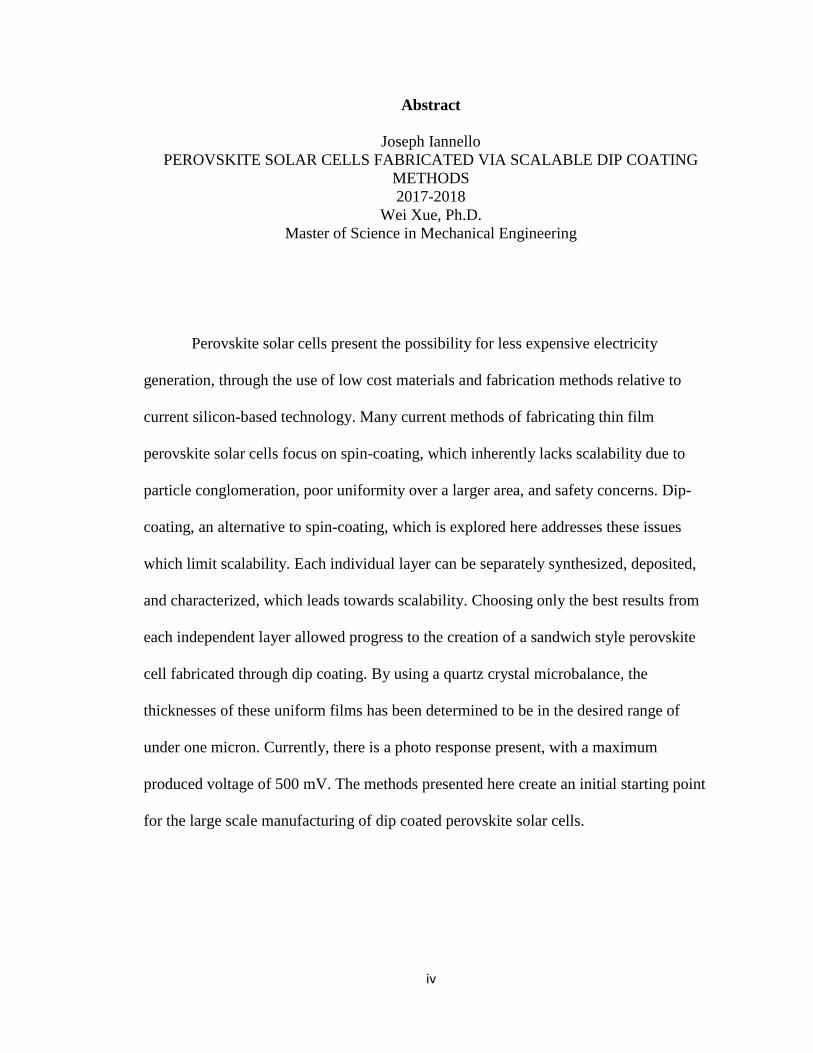
The BP statistical review reports that during the calendar year 2016, 18.2 TW of
energy was consumed globally[1]. 3.06% of this energy consumed was generated by
renewable sources, other than hydroelectricity, or nuclear power. Solar energy was
responsible for only 0.048% of total energy consumed, which amounts to 8.79 GW.
Figure 1 presents a detailed breakdown of energy consumption by each produced method.
Each year, 23000 TW of available energy hits the Earth’s surface as radiation from the
sun, which far exceeds the consumption of the Human population. The largest obstacle
for solar energy production to overcome is cost.
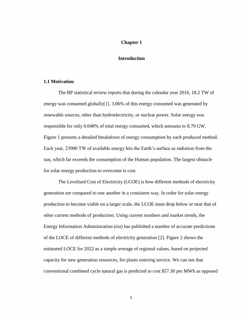
The Levelised Cost of Electricity (LCOE) is how different methods of electricity
generation are compared to one another in a consistent way. In order for solar energy
production to become viable on a larger scale, the LCOE must drop below or near that of
other current methods of production. Using current numbers and market trends, the
Energy Information Administration (eia) has published a number of accurate predictions
of the LOCE of different methods of electricity generation [2]. Figure 2 shows the
estimated LOCE for 2022 as a simple average of regional values, based on projected
capacity for new generation resources, for plants entering service. We can see that
conventional combined cycle natural gas is predicted to cost $57.30 per MWh as opposed
2
to PV solar, which is $85.00 per MW. Even with four years of technological
advancements, this puts solar at a cost of 148% of conventional combined cycle natural
gas, which is one of the biggest reasons for finding ways to reduce costs of photovoltaic
cells even further.
Figure 1. Energy consumed globally, by type, for the year of 2017, in terawatt hours
according to the BP statistical review of world energy[1].
3.73
4.34
5.14
0.69
1.06
0.01 0.00
1.00
2.00
3.00
4.00
5.00
6.00
Natural Gas Coal Oil Nuclear Power Hydroelectric Solar Power
Ter
raw
att
Hours
Energy Form
3
Figure 2. The predicted LCOE for various types of energy generation according to the
eia[2].
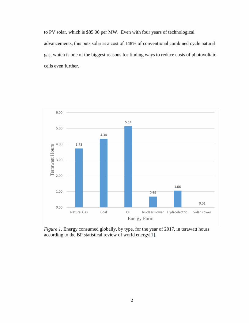
Currently produced solar panels are part of what is called the first generation of
solar panels. These are made of silicon, and come in two types, monocrystalline, and
polycrystalline. The biggest differences between these two types are efficiency, and
production cost. Figure 3 shows the current best research efficiencies photovoltaic cells.
This is a yearly graph which details current best production methods, from 1975 until
2017. Looking at the year for 2017, the blue line represents silicon cells, and the highest
efficiency is for monocrystalline, at around 28%, while polycrystalline are slightly lower,
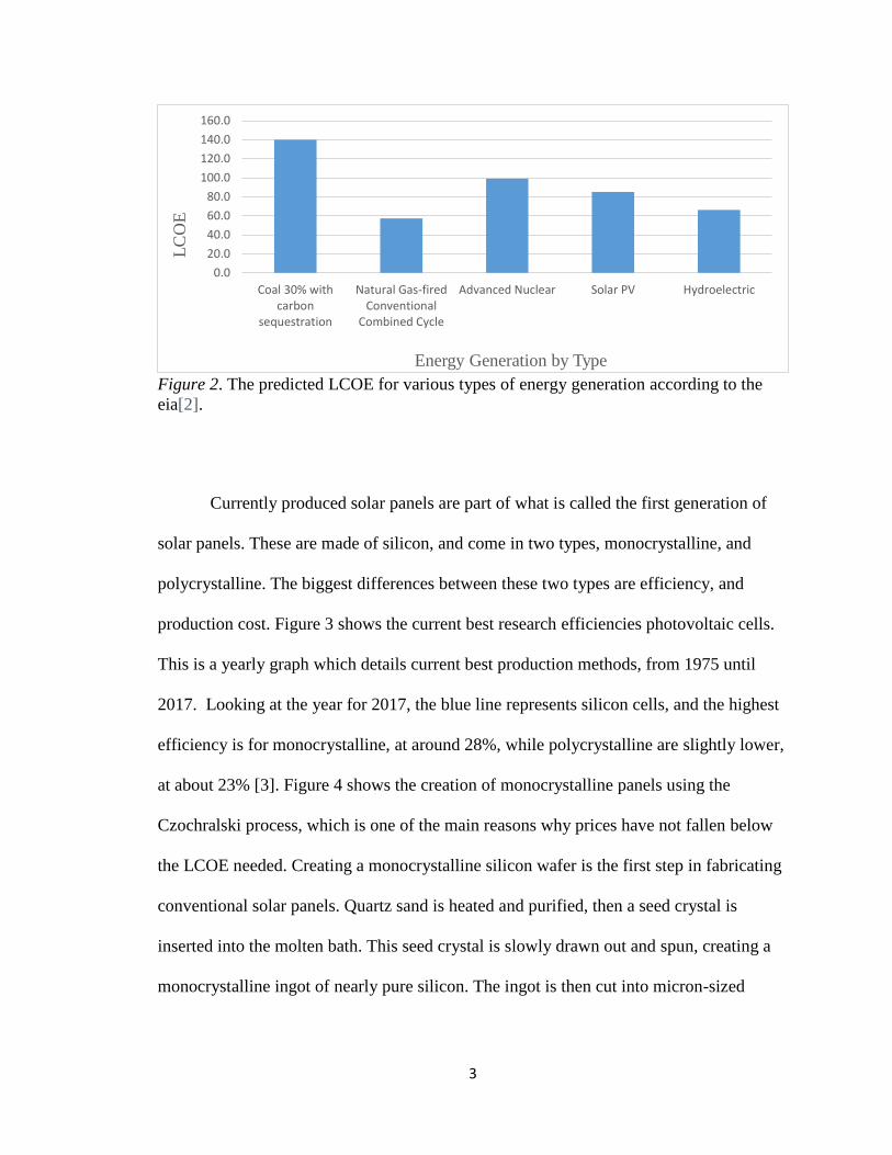
at about 23% [3]. Figure 4 shows the creation of monocrystalline panels using the
Czochralski process, which is one of the main reasons why prices have not fallen below
the LCOE needed. Creating a monocrystalline silicon wafer is the first step in fabricating
conventional solar panels. Quartz sand is heated and purified, then a seed crystal is
inserted into the molten bath. This seed crystal is slowly drawn out and spun, creating a
monocrystalline ingot of nearly pure silicon. The ingot is then cut into micron-sized
0.0
20.0
40.0
60.0
80.0
100.0
120.0
140.0
160.0
Coal 30% withcarbon
sequestration
Natural Gas-firedConventional
Combined Cycle
Advanced Nuclear Solar PV Hydroelectric
LC
OE
Energy Generation by Type

4
wafers, etched, and polished, before being sent to another facility where dopants are
added and the final panel is constructed.
Figure 3. Best research cell efficiencies from 1975 until 2017 from the National
Renewable Energy Laboratory [3].

5
Figure 4. The method of fabricating pure silicon wafers is known as the Czochralski
process.
The second generation of solar cells are thin film solar cells, usually fabricated
using the element cadmium. While efficiencies are comparable to those of silicon, the
rarity and high toxicity of cadmium has prevented this technology from reaching its full
potential, and second generation panels only make up about 10% of the current market
share. The third generation of photovoltaic cells include dye sensitized solar cells
(DSSCs), quantum dots, and perovskite solar cells. While DSSCs and quantum dots have
showed promise, they have their limitations which must be overcome before they can be
brought to market. Most notably, DSSCs contain liquid and biological matter, which
leave them open to decomposing and vulnerable to the elements. Quantum dots, while
individually tunable, are expensive to make, and highly toxic. Perovskite, the third
material classified as a Generation-3 solar cell material, has shown an exceptional
increase in performance since its inception. Figure 3 shows this marked increase in
Cutting Ingot
into Wafers
Crystal Furnace Edge Grinding and
Flattening
Crystal Etching and
Polishing
Wafer Cleaning and
Particle RemovalButtonLaser Inspection
Finished Silicon Wafer
Crystal Growth
and Shaping

6
efficiency. The orange line with yellow circles represents perovskites, in 8 years, the
efficiency of perovskite solar cells has risen almost 20%. The first perovskite cell was
described in 2009, and had an efficiency of 3.8%[4]. Since then, advancements in this
field have improved drastically, with the highest verified efficiency now at 22.7%,
measured in 2017 [3].This large increase in efficiency in such a short time, combined
with low material cost, are two of the biggest reasons why perovskite solar cells have
attracted so much attention.
1.2 Background
Perovskite was first discovered in 1839 by Gustav Rose in the Ural Mountains of
Russia, and was named after a famous geologist at the time, Lev Perovski. The
discovered mineral had a chemical formula of CaTiO3. Figure 5 shows this general
chemical formula of ABX3, which leads to the ideal perovskite structure, within a certain
tolerance [5]. This tolerance is known as the Goldschmidt tolerance factor, which was
first described by Victor Moritz Goldschmidt in 1926. The Goldschmidt tolerance factor
is based on the ionic radii of the elements that make up the perovskite crystal, and is
defined by the following equation [6, 7],
where 𝑟𝐴 is the radius of the A-cation, 𝑟𝐵 is the radius of the B-cation, and 𝑟0 is the radius
of the anion. An ideal cubic perovskite structure of the unit cell (a) is defined by the
following equation [5].
𝑡 =
𝑟𝐴 + 𝑟0
√2(𝑟𝐵 + 𝑟0)
(1.1)
𝑎 = √2(𝑟𝐴 + 𝑟0) = 2(𝑟𝐵 + 𝑟0)
(1.2)

7
A stable, cubic, perovskite structure occurs if 0.89 < t < 1, which means that the cations
are of ideal size [5].
Figure 5. The general structure of a perovskite crystal.
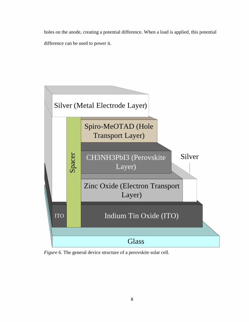
Perovskite solar cells are constructed in a sandwich style, using multiple layers of
thin films to harvest light [8]. Figure 6 shows the general style of a perovskite cell, which
has remained relatively unchanged since their inception. These cells work on the
principal of the photoelectric effect and exciton generation. Excitons are generated in the
perovskite by light, once generated, the holes and electrons follow the path of least
resistance through their respective layers. Electrons are then collected on the cathode, and
X
A
B
8
holes on the anode, creating a potential difference. When a load is applied, this potential
difference can be used to power it.
Figure 6. The general device structure of a perovskite solar cell.
Glass
Indium Tin Oxide (ITO)
Zinc Oxide (Electron Transport
Layer)
CH3NH3PbI3 (Perovskite
Layer)
Spiro-MeOTAD (Hole
Transport Layer)
ITO
Silver (Metal Electrode Layer)
Spac
er Silver
9
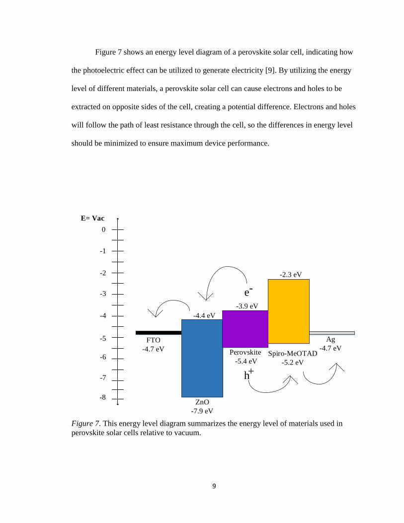
Figure 7 shows an energy level diagram of a perovskite solar cell, indicating how
the photoelectric effect can be utilized to generate electricity [9]. By utilizing the energy
level of different materials, a perovskite solar cell can cause electrons and holes to be
extracted on opposite sides of the cell, creating a potential difference. Electrons and holes
will follow the path of least resistance through the cell, so the differences in energy level
should be minimized to ensure maximum device performance.
Figure 7. This energy level diagram summarizes the energy level of materials used in
perovskite solar cells relative to vacuum.
-5
-4
-1
0
-2
-3
-6
-8
-7
FTO
-4.7 eV
E= Vac
ZnO
-7.9 eV
Perovskite
-5.4 eVSpiro-MeOTAD
-5.2 eV
Ag
-4.7 eV
-2.3 eV
-3.9 eV
-4.4 eV
e-
h+

10
The Shockley-Queisser limit for a single junction solar cell defines a maximum
efficiency of 33.7%, with a band-gap of 1.37 eV[10]. The first, most commonly used, and
most efficient perovskites so far, have a chemical formula of CH3NH3PbI3, which is in
line with the general ABX3 formula for a perovskite [4, 8, 11]. These perovskites are
formed according to the following reaction
CH3NH3I+PbI2 -> CH3NH3PbI3 (1.3)
CH3NH3I is also known as methylammonium iodide or MAI. To date, many successful
MAI lead-based perovskite cells have a band-gap of 1.56 eV, corresponding to a
theoretical maximum efficiency of 31.3 [12]. This is comparable to silicon, which has a
band-gap of 1.1 eV and a maximum theoretical efficiency of about 32%. Band-gaps of
perovskites can be tuned anywhere from 1.17 – 1.56 by changing doping ratios of Sn+2
and Pb+2 [13]. This tunability also allows for a variety of differences between designs
based on the electron transport layer, and the hole transport layer, as well as allowing for
the possibility multi-junction perovskite solar cells.
Current, most high performance perovskite solar cells are fabricated using a
method known as spin coating [8, 14]. Figure 8 shows a current method of spin coating,
which revolves around the concept of spinning substrates at a high speed to produce
uniform thin films. While spin coating produces reliable results which are replicated
easily in a laboratory setting, spin coating fundamentally lacks scalability due to a variety
of factors. One large issue is that spin coating only produces uniform films on small
areas. As the desired area becomes larger, particles start to aggregate and produce large
clumps in lines radially along the substrate. Another issue is safety, the larger the
substrate, the greater the risk of damage if something fails and the substrate becomes

11
unattached to the spin coater.
Figure 8. Current spin coating methods rely on a two-step method which involves
spinning substrates at high rpm’s.
1.3 Objectives
As spin-coating inherently lacks scalability, other alternatives must be
investigated. Current published alternatives include roll-to-roll processing, spray coating,
and slot-die coating [15-18]. Slot-die coating is a typical large-scale manufacturing
process. The desired chemical, in this case, lead iodide, is sent through a small channel,
which is the slot, with an additional slot blowing out an inert gas, usually nitrogen, which
follows immediately behind it. By taking these slots and quickly moving them across a
substrate, thin films of lead iodide of relatively good uniformity can be produced. Though
TiO2 PbI2 CH3NH3I CH3NH3PbI3
HEAT
PbI2 CH3NH3I

12
advancements have been made using these processing methods, producing uniform films
which cover a large area have still been a challenge. Stability is also an issue, as ambient
moisture will degrade the perovskite, all devices must be encapsulated to ensure there is
no degradation. The primary objectives of investigating the large scale manufacturing of
perovskites is the purpose of this thesis, and is done so through dip-coating. By
fabricating, characterizing, and optimizing each individual layer of a perovskite solar cell,
an entire cell can be fabricated through dip-coating. Figure 9 shows the general process
of dip coating for an entire perovskite cells, except the top electrode. A substrate is
dunked into a container of the desired chemical, and then dried. Depending on the
number of dips, concentration of the solution, dipping angle, and drying angle, thin films
of varying thicknesses and uniformities can be fabricated. By choosing the most uniform
films for each step and continuing, a clear photo response is observed.

13
Figure 9. Fabrication of a perovskite solar cell through dip coating.
FTO
ZnOHEAT
DIP ZnO
ZnO
PbI2
DIPPbI2
HEAT
PbI2
CH3NH3I
HEAT
Spiro-
MeOTAD
CH3NH3PbI3
CH3NH3PbI3
HEAT
Spiro-
MeOTAD

14
Chapter 2
Electron Transport Layer
Described in the following chapter are multiple synthesis methods for different
types of zinc oxide particles, which can be used a material for the electron transport layer.
Titanium dioxide was also investigated, but due to the high temperature required for
annealing, zinc oxide was chosen as the desired material. Types of zinc oxide particles
include nano-rods, stock nanoparticles, and synthesized nanoparticles. As uniformity is
the biggest issue for large-scale manufacturing, a scanning electron microscope was used
to identify topographical information about the deposited layers. The most uniform layer,
within the desired thickness, was fabricated using synthesized zinc oxide nano-particles.
2.1 Zinc Oxide Nano-Rod Fabrication
Referring back to Figure 6, there are various layers involved in a perovskite solar
cell. Each of these layers are composed of different materials, some of which must first
be synthesized prior to deposition. A reasonable starting position was the electron
transport layer (ETL), which is most often composed of either titanium dioxide or zinc
oxide [19-22]. As low cost and low temperature were objectives, it was decided that zinc
oxide would be the material of choice. This is due to the fact that titanium dioxide thin
films require a very high annealing temperature, on the order of 400-500°C [23-25]. A
high temperature annealing step would not only drive up costs, but also limit the
substrates on which the films can be deposited. As a bendable cell on a plastic substrate
was a desired outcome, zinc oxide was chosen.
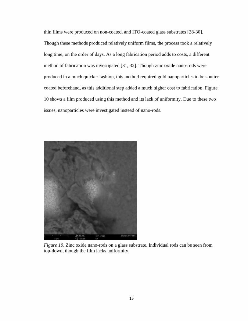
Known for their high carrier concentration, zinc oxide nano-rod thin films were
the starting point for this layer [26, 27]. Following known methods, zinc oxide nano-rod
15
thin films were produced on non-coated, and ITO-coated glass substrates [28-30].
Though these methods produced relatively uniform films, the process took a relatively
long time, on the order of days. As a long fabrication period adds to costs, a different
method of fabrication was investigated [31, 32]. Though zinc oxide nano-rods were
produced in a much quicker fashion, this method required gold nanoparticles to be sputter
coated beforehand, as this additional step added a much higher cost to fabrication. Figure
10 shows a film produced using this method and its lack of uniformity. Due to these two
issues, nanoparticles were investigated instead of nano-rods.
Figure 10. Zinc oxide nano-rods on a glass substrate. Individual rods can be seen from
top-down, though the film lacks uniformity.
16
2.2 Sol-Gel Method
Investigation of the zinc oxide nano-particles revealed several methods of
synthesis exist, many of which produce very reliable, uniform films of zinc oxide [33-
35]. The most common method involves creation of a sol-gel using a precursor of either
zinc nitrate of zinc chloride. A substrate is then momentarily placed into the gel and
quickly removed, then the substrate is dried at a temperature, usually around 100 °C, and
annealed at a much higher temperature, usually around 400 °C. By investigating
structural and optical properties of zinc oxide films, a separate synthesis method was
proposed which did not involve annealing at a high temperature [33, 36-38]. A sol-gel
solution was prepared by the following method.
A 0.1 molar solution of zinc nitrate was prepared by dissolving 3.2695 g of mossy
zinc in a minimal amount of nitric acid, and then adding this to 500 mL of deionized
water. A 0.1 molar solution of ammonium hydroxide was prepared by adding 8.81 mL of
25% weight ammonium hydroxide to 491.91 mL of deionized water. The 0.1 molar
solution of zinc nitrate was then added dropwise at 1 mL per minute to the 0.1 molar
ammonium hydroxide solution, over the course of 15 minutes, for a total of 15 mL of the
zinc oxide solution added. The solution was then allowed to sit for 10 minutes, as a sol-
gel began to form. After 10 minutes, substrates were vertically dipped, and dried
horizontally for 10 minutes at 120 °C for 10 minutes after each dip. A total of five dips
were performed, and a visible layer was added to the substrate. Figure 11 presents a
detailed description of the film, image (a) shows an overall view of the film, while image
(b) represents a closer view. Though zinc oxide nano-rods and particles were present,
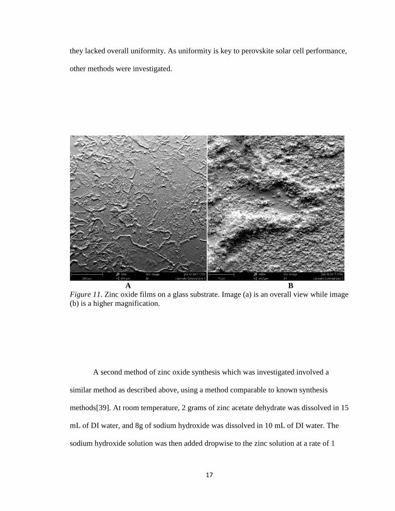
17
they lacked overall uniformity. As uniformity is key to perovskite solar cell performance,
other methods were investigated.
A B
Figure 11. Zinc oxide films on a glass substrate. Image (a) is an overall view while image
(b) is a higher magnification.
A second method of zinc oxide synthesis which was investigated involved a
similar method as described above, using a method comparable to known synthesis
methods[39]. At room temperature, 2 grams of zinc acetate dehydrate was dissolved in 15
mL of DI water, and 8g of sodium hydroxide was dissolved in 10 mL of DI water. The
sodium hydroxide solution was then added dropwise to the zinc solution at a rate of 1
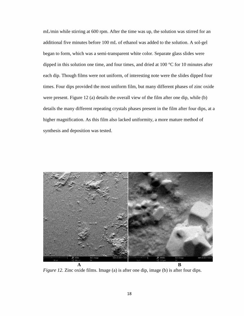
18
mL/min while stirring at 600 rpm. After the time was up, the solution was stirred for an
additional five minutes before 100 mL of ethanol was added to the solution. A sol-gel
began to form, which was a semi-transparent white color. Separate glass slides were
dipped in this solution one time, and four times, and dried at 100 °C for 10 minutes after
each dip. Though films were not uniform, of interesting note were the slides dipped four
times. Four dips provided the most uniform film, but many different phases of zinc oxide
were present. Figure 12 (a) details the overall view of the film after one dip, while (b)
details the many different repeating crystals phases present in the film after four dips, at a
higher magnification. As this film also lacked uniformity, a more mature method of
synthesis and deposition was tested.
A B
Figure 12. Zinc oxide films. Image (a) is after one dip, image (b) is after four dips.

19
2.3 Zinc Oxide Nanoparticles
As nanoparticles of zinc oxide can be synthesized with relative ease, a different
approach was taken. Stock zinc oxide particles were purchased from Nanoamore, which
had an average particle size of 30 nm. As these particles were coated in silicone oil to
prevent aggregation, the oil had to be stripped off first. 600 mg of the zinc oxide powder
was dispersed in 50 mL of toluene and stirred at 600 rpm for 5 minutes at room
temperature. The toluene was decanted off and the zinc oxide was spun in a centrifuge for
5 minutes at 4000 rpm, also at room temperature. The powder was then washed twice
with 40 mL of methanol and dried at 80 °C. After this a solution of 65 mL of n-butanol, 5
mL of chloroform, and 5 mL of methanol was mixed, and zinc oxide powder was added
to make a solution with a concentration of 6 mg per mL [8]. Figure 13 details the
coverage of this film. Even after 5 dips in this solution, there was incredibly poor
coverage on all areas of the substrate. As this was very different than previous films, it
was decided that synthesized nanoparticles should be used instead of ones purchased
from a vendor.

20
A B
Figure 13. Zinc oxide films from stock nano-particles, (a) presents and overall view
while (b) is more magnified.
Nanoparticles were synthesized in the lab according to the literature, and
dispersed in the a solution for deposition on a substrate [8]. Glass slides were dipped into
the solution between one and five times, with a 3 minute dry at 80 °C between each dip.
The films could be visibly seen with the human eye, and were mostly transparent, with
coloration towards the edges. The edges of the films were wiped clean while the film was
wet during cell fabrication to solve the uniformity issues at the edges. Figure 14 present
SEM images of the film after one dip. The film is uniform, with complete coverage of the
substrate as seen in image (a). In order to see the film, a scratch was etched into it with
tweezers, as seen in image (b) One dip was chosen due to the thickness being closest to
the desired value of about 70 nm [8, 40, 41].
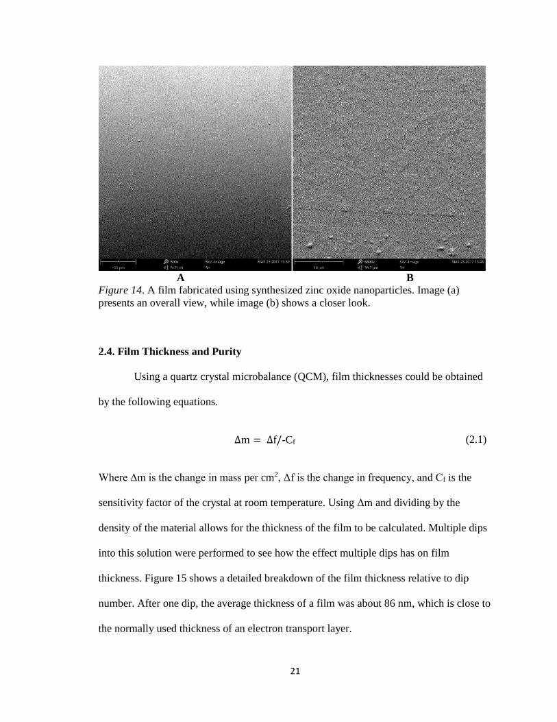
21
A B
Figure 14. A film fabricated using synthesized zinc oxide nanoparticles. Image (a)
presents an overall view, while image (b) shows a closer look.
2.4. Film Thickness and Purity
Using a quartz crystal microbalance (QCM), film thicknesses could be obtained
by the following equations.
Δm = Δf/-Cf
(2.1)
Where Δm is the change in mass per cm2, Δf is the change in frequency, and Cf is the
sensitivity factor of the crystal at room temperature. Using Δm and dividing by the
density of the material allows for the thickness of the film to be calculated. Multiple dips
into this solution were performed to see how the effect multiple dips has on film
thickness. Figure 15 shows a detailed breakdown of the film thickness relative to dip
number. After one dip, the average thickness of a film was about 86 nm, which is close to
the normally used thickness of an electron transport layer.
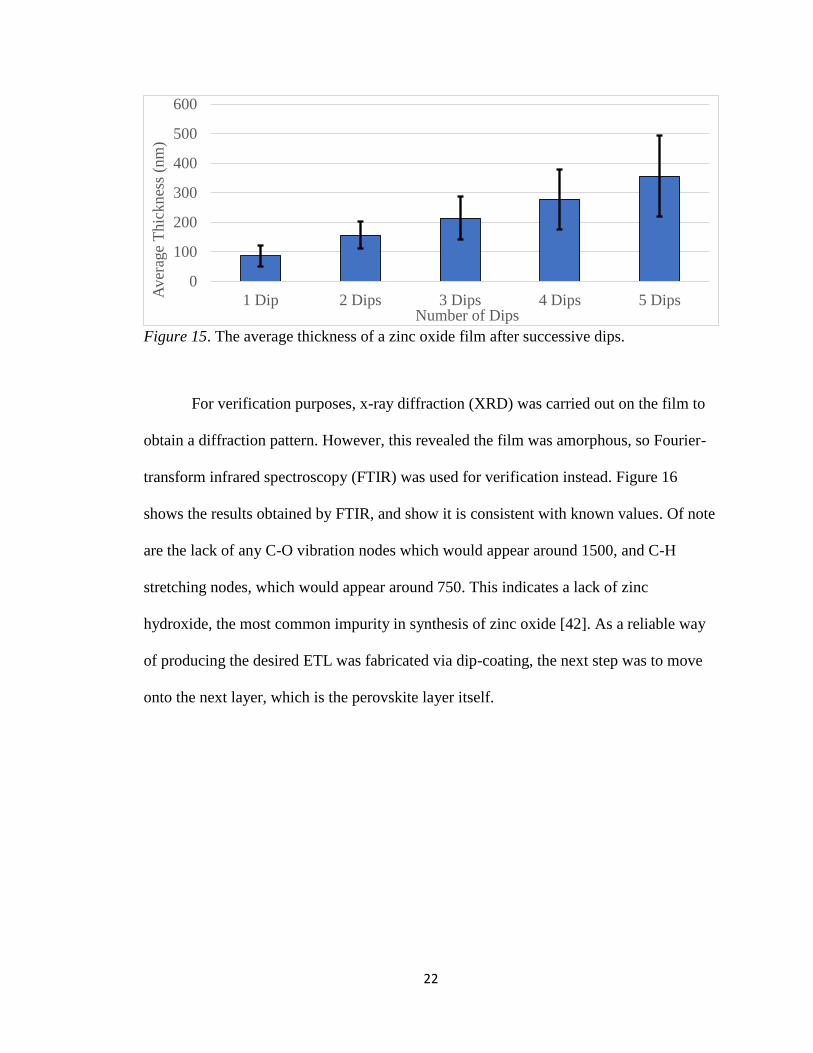
22
Figure 15. The average thickness of a zinc oxide film after successive dips.
For verification purposes, x-ray diffraction (XRD) was carried out on the film to
obtain a diffraction pattern. However, this revealed the film was amorphous, so Fourier-
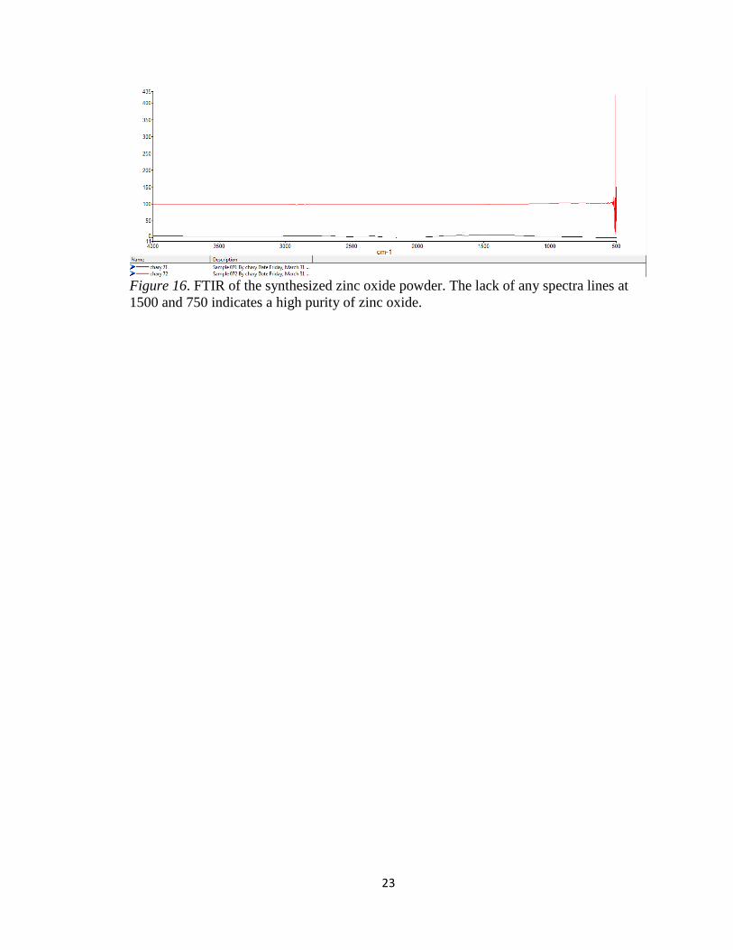
transform infrared spectroscopy (FTIR) was used for verification instead. Figure 16
shows the results obtained by FTIR, and show it is consistent with known values. Of note
are the lack of any C-O vibration nodes which would appear around 1500, and C-H
stretching nodes, which would appear around 750. This indicates a lack of zinc
hydroxide, the most common impurity in synthesis of zinc oxide [42]. As a reliable way
of producing the desired ETL was fabricated via dip-coating, the next step was to move
onto the next layer, which is the perovskite layer itself.
0
100
200
300
400
500
600
1 Dip 2 Dips 3 Dips 4 Dips 5 DipsAver
age
Thic
knes
s (n
m)
Number of Dips
23
Figure 16. FTIR of the synthesized zinc oxide powder. The lack of any spectra lines at
1500 and 750 indicates a high purity of zinc oxide.

24
Chapter 3
Lead Iodide and Perovskite
As perovskite thin films are typically fabricated using two-step spin coating, a
similar process was developed for spray coating and dip coating. First, in order to
minimize costs, films were fabricated without a solvent, using a two-step dip coating
method, in order to test viability. As these films were not within the desired thickness
range, a decision was then made to use a solvent in order to assist in deposition.
Dimethylformamide and dimethyl sulfoxide, a common two common solvents, were used
to dissolve lead iodide in order to test spray and dip coating. Films fabricated by spray
coating were prone to large structure formation, while films fabricated through dip-
coating were much more uniform. Using these lead iodide films as a precursor gave very
uniform perovskite films, which were synthesized at a low temperature in ambient air.
3.1 Lead Iodide
Typical MAI perovskite based films are constructed using a two-step method
which involves lead iodide as a precursor film [43, 44]. As low-cost solar cells were the
main objective, the aim was to use no or minimal solvents during the initial stages of the
project. Using this as a starting point, lead iodide films were created using a two-step
coating process with the typical reaction of lead nitrate and potassium iodide, according
to equation 3.1.
Pb(NO3)2 + 2KI => 2KNO3 + PbI2 (3.1)
3.2 Fabrication of Lead Iodide Films Without a Solvent
Aqueous lead nitrate was synthesized by dissolving 0.1 moles of lead powder
with a minimal amount of nitric acid, and then adding this to one liter of water and
25
allowing it to dissolve completely. Aqueous potassium iodide was synthesized by
dissolving 0.2 moles of potassium iodide into 1 liter of water. About 100 mL of each of
these solutions were put into separate beakers, to avoid cross contamination during
fabrication. Glass slides were first dipped into the lead nitrate solution, and then
immediately dipped into the potassium iodide solution. After the dip into the potassium
nitrate solution, a visible lead iodide film could be seen, the slides were immediately
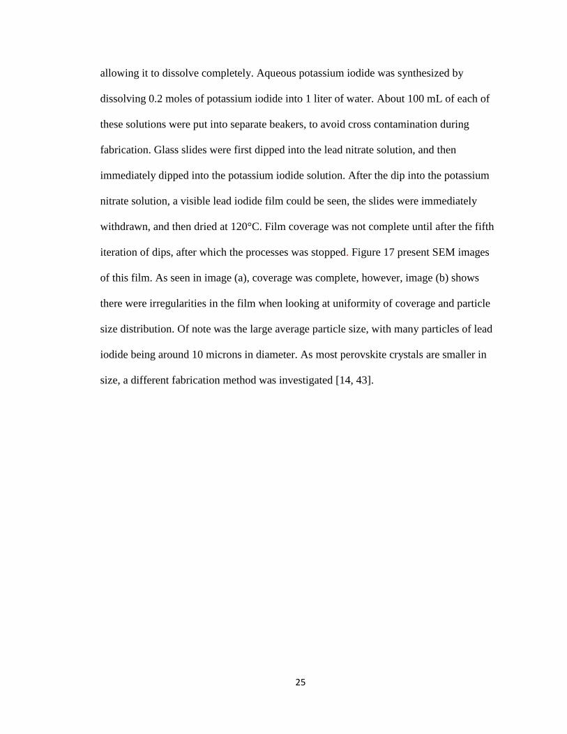
withdrawn, and then dried at 120°C. Film coverage was not complete until after the fifth
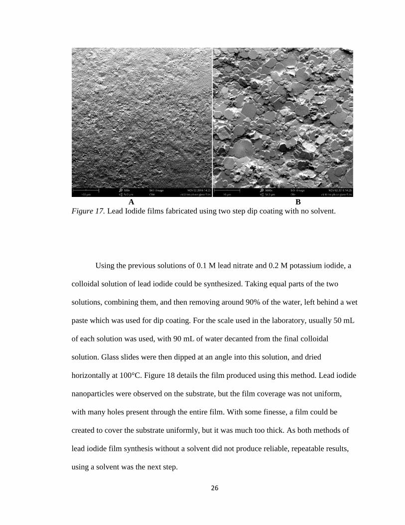
iteration of dips, after which the processes was stopped. Figure 17 present SEM images
of this film. As seen in image (a), coverage was complete, however, image (b) shows
there were irregularities in the film when looking at uniformity of coverage and particle
size distribution. Of note was the large average particle size, with many particles of lead
iodide being around 10 microns in diameter. As most perovskite crystals are smaller in
size, a different fabrication method was investigated [14, 43].
26
A B
Figure 17. Lead Iodide films fabricated using two step dip coating with no solvent.
Using the previous solutions of 0.1 M lead nitrate and 0.2 M potassium iodide, a
colloidal solution of lead iodide could be synthesized. Taking equal parts of the two
solutions, combining them, and then removing around 90% of the water, left behind a wet
paste which was used for dip coating. For the scale used in the laboratory, usually 50 mL
of each solution was used, with 90 mL of water decanted from the final colloidal
solution. Glass slides were then dipped at an angle into this solution, and dried
horizontally at 100°C. Figure 18 details the film produced using this method. Lead iodide
nanoparticles were observed on the substrate, but the film coverage was not uniform,
with many holes present through the entire film. With some finesse, a film could be
created to cover the substrate uniformly, but it was much too thick. As both methods of
lead iodide film synthesis without a solvent did not produce reliable, repeatable results,
using a solvent was the next step.

27
A B
Figure 18. SEM images of colloidal lead iodide films dip coated without a solvent.
3.3 Fabrication of Lead Iodide Films With a Solvent
It has been shown that colloidal particles and spray-coating have a wide variety of
applications, not limited to perovskites [45]. As spray-coating perovskite solar cells
using lead iodide in a solvent have been constructed in the past, this was used as a
starting point [15, 17]. Dimethylformamide (DMF) and dimethyl sulfoxide (DMSO) are
the two most commonly used solvents for this purpose, therefore these two solvents were
chosen for spray-coating [46, 47]. Films constructed using DMSO are not imaged, as they
were visibly non-uniform to the human eye, with lead iodide crystals forming which were
multiple millimeters long.
3.3.1. Spray coating. Films were fabricated by using a normal spray bottle and
nozzle, which can be found in any laboratory. Firstly, lead iodide was dissolved in DMF

28
at a concentration of 460 mg ml-1, which is one of the standard concentrations for spin
coating lead iodide films for perovskite solar cells [8]. Films were fabricated by spraying
on a certain number of sprays, and then drying the substrate at 100°C for about 5 minutes
in an oven. Just using one spray covered most of the small substrate, but there were
irregularities such as striations and pinholes in the film. As irregularities in perovskite
solar cells can drastically hinder performance, more coatings were fabricated to see if
these striations could be removed or filled in. Figure 19, image (a) details a film
fabricated using three sprays, with a drying in between each spray, which can be
compared to image (b) which had a drying step only at the end. When a film is allowed to
dry between each spray, the uniformity improves, seen by the lack of pin-holes and
striations in the film. However, if too much lead iodide is applied, then micro rods of lead
iodide begin to form, which causes non-uniformity in a different way.

29
A B
Figure 19. Spray coated lead iodide film fabricated by spraying three times.
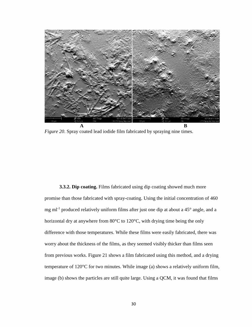
Figure 20 shows how this effect can easily be seen, as there are rods of lead
iodide measuring well over 100 microns long are present in the films. This figure
presents two lead iodide films fabricated using nine sprays. Image (a) had a drying step in
between each spray, and image (b) was only dried after all 9 spray were completed. As
none of the spray-coating methods showed promising results, a decision was made to see
how films fabricated using dip coating with solvents appeared.
30
A B
Figure 20. Spray coated lead iodide film fabricated by spraying nine times.
3.3.2. Dip coating. Films fabricated using dip coating showed much more
promise than those fabricated with spray-coating. Using the initial concentration of 460
mg ml-1 produced relatively uniform films after just one dip at about a 45° angle, and a
horizontal dry at anywhere from 80°C to 120°C, with drying time being the only
difference with those temperatures. While these films were easily fabricated, there was
worry about the thickness of the films, as they seemed visibly thicker than films seen
from previous works. Figure 21 shows a film fabricated using this method, and a drying
temperature of 120°C for two minutes. While image (a) shows a relatively uniform film,
image (b) shows the particles are still quite large. Using a QCM, it was found that films
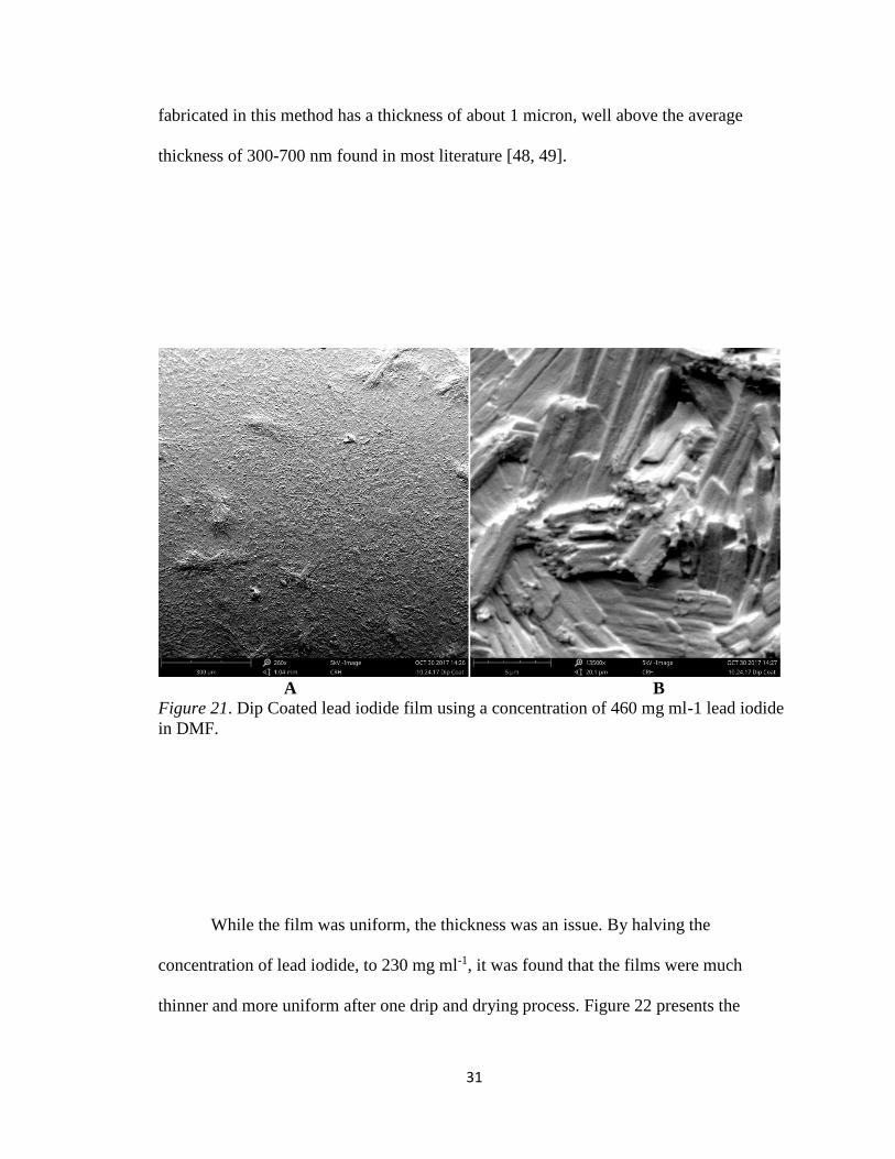
31
fabricated in this method has a thickness of about 1 micron, well above the average
thickness of 300-700 nm found in most literature [48, 49].
A B
Figure 21. Dip Coated lead iodide film using a concentration of 460 mg ml-1 lead iodide
in DMF.
While the film was uniform, the thickness was an issue. By halving the
concentration of lead iodide, to 230 mg ml-1, it was found that the films were much
thinner and more uniform after one drip and drying process. Figure 22 presents the
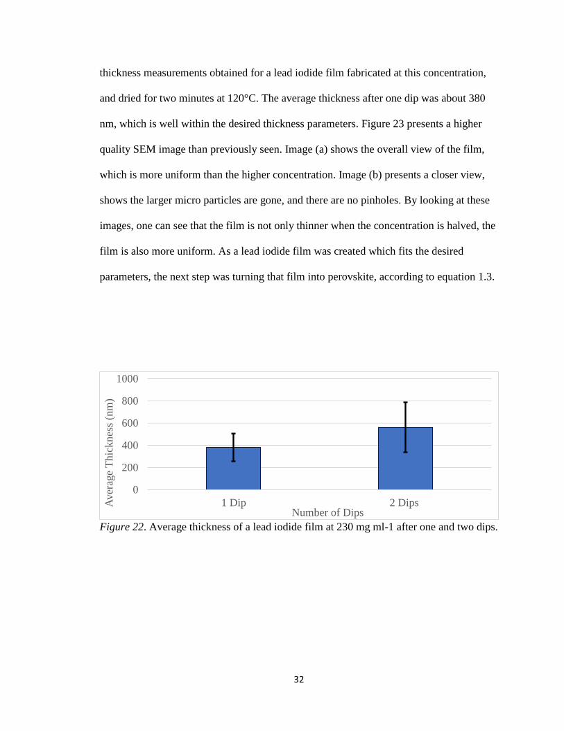
32
thickness measurements obtained for a lead iodide film fabricated at this concentration,
and dried for two minutes at 120°C. The average thickness after one dip was about 380
nm, which is well within the desired thickness parameters. Figure 23 presents a higher
quality SEM image than previously seen. Image (a) shows the overall view of the film,
which is more uniform than the higher concentration. Image (b) presents a closer view,
shows the larger micro particles are gone, and there are no pinholes. By looking at these
images, one can see that the film is not only thinner when the concentration is halved, the
film is also more uniform. As a lead iodide film was created which fits the desired
parameters, the next step was turning that film into perovskite, according to equation 1.3.
Figure 22. Average thickness of a lead iodide film at 230 mg ml-1 after one and two dips.
0
200
400
600
800
1000
1 Dip 2 DipsAver
age
Thic
knes
s (n
m)
Number of Dips

33
A
B
Figure 23. Dip coated lead iodide film fabricated using a concentration of 230 mg ml-1
lead iodide in DMF.
3.4 Perovskite Synthesis
Perovskite films synthesized via a two-step reaction are typically characterized
using XRD. A sample was prepared using colloidal lead iodide as seen in figure 18, and
reacted by dipping the film in a solution of MAI in 2-propanol at a concentration of 10
mg ml-1 for five minutes, and then drying the film at 80°C for five minutes. The resulting
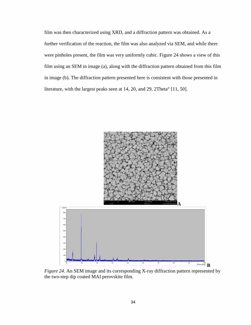
34
film was then characterized using XRD, and a diffraction pattern was obtained. As a
further verification of the reaction, the film was also analyzed via SEM, and while there
were pinholes present, the film was very uniformly cubic. Figure 24 shows a view of this
film using an SEM in image (a), along with the diffraction pattern obtained from this film
in image (b). The diffraction pattern presented here is consistent with those presented in
literature, with the largest peaks seen at 14, 20, and 29, 2Theta° [11, 50].
A
B Figure 24. An SEM image and its corresponding X-ray diffraction pattern represented by
the two-step dip coated MAI perovskite film.
35
As pinholes are an inherent problem with recombination between the ETL and
HTL, the perovskite films must be annealed to reach their best efficiency [50, 51]. Lead
iodide films were prepared by two-step coating using DMF as the solvent. Then, MAI
was dripped on to the film, with enough for some excess MAI to be present during
drying. Films were then annealed for five minutes, after which more MAI was dripped
onto the film. The film was then inserted back into the oven to finish the dry and anneal
process. The annealing step was originally at a lower temperature of 90°C, however, this
temperature proved to be too low, as even after 45 minutes of annealing at this
temperature, pinholes were visible in the film. Uniformity of the lead iodide precursor did
have an effect on the uniformity of the perovskite, but it was ultimately the annealing step
which could remove imperfections at the nano-scale. By increasing the temperature to
120°C and lowering the time to 5 minutes for the first drip of MAI, and then 2 minutes
for the second drip, the pinholes were no longer present. Figure 25 shows a comparison
between annealing at 90°C for 45 minutes (image (a)), and annealing at 120°C for 7
minutes (image (b)). The film annealed at a higher temperature was more uniform, and
the distinctive cubic crystal perovskite phase expected was still present in the film, which
shows the film did not degrade at the higher temperature. Films created using this method
did not visibly degrade as long as they were kept at relatively low humidity, below 40%.
The fabrication of a perovskite film via which was pin-hole free meant that the final two
layers could be constructed on top, first the hole transport layer, followed by the top
electrode.

36
A
B
Figure 25. A comparison of perovskite films annealed at two separate temperatures.

37
Chapter 4
Hole Transport Layer, Top Electrode and Testing
The hole-transport layer is the penultimate layer of the solar cell. The most
commonly used material is called Spiro-MeOTAD. Spiro-MeOTAD itself does not allow
for the transport of holes, but with the use of p-type dopants, it can. As Spiro-MeOTAD
is expensive, an alternative material called copper(I) thiocyanate (CuSCN) was also
investigated. The films fabricated using CuSCN were not uniform, and much too thick.
As such, even though Spiro-MeOTAD is more expensive, it is the preferred material of
choice. The top electrode is usually silver or gold, due to the work function of the metal.
Here, silver was used in order to keep costs low. The top electrode is typically deposited
using sputtering, but silver paste was also investigated. The best performing cells were
ones which had a Spiro-MeOTAD HTL, and a silver electrode deposited through
sputtering.
4.1 Spiro-MeOTAD
Referring back to figure 7, following deposition of the perovskite layer, a hole-
transport layer must be fabricated on top of it. This layer allows holes to freely pass
through it, but does not allow electrons to. Due to this property, there are very few
choices of materials, as these are highly specialized. A material called Spiro-MeOTAD
(C81H68N4O8) has been commonly used in perovskite solar cells for years [52, 53]. Spiro-
MeOTAD is a highly expensive compound which requires powerful dopants to be used
effectively as a hole-transport material, but is unrivaled in its performance [54, 55]. Due
to this primary constraint of cost, and the inherent degradation of leftover material, drip
coating was investigated for this layer. Literature review conducted about this materials

38
showed that uniformity is heavily dependent on the previous layer, and slot-die coating
had produced uniform films previously [18]. Using this knowledge as a baseline, Spiro-
MeOTAD was prepared according to known practices [8]. Spiro-MeOTAD was then
dripped onto previously prepared perovskite film 5 microliters at a time, until the whole
film was visibly covered. Excess Spiro-MeOTAD was wiped clean, and then the film was
placed into an oven at 100°C for two minutes, to allow the film to dry completely. When
removed, the film had turned from a dull black, to a shiny black, indicating the Spiro-
MeOTAD was present on top of the perovskite. There were no visible ridges present in
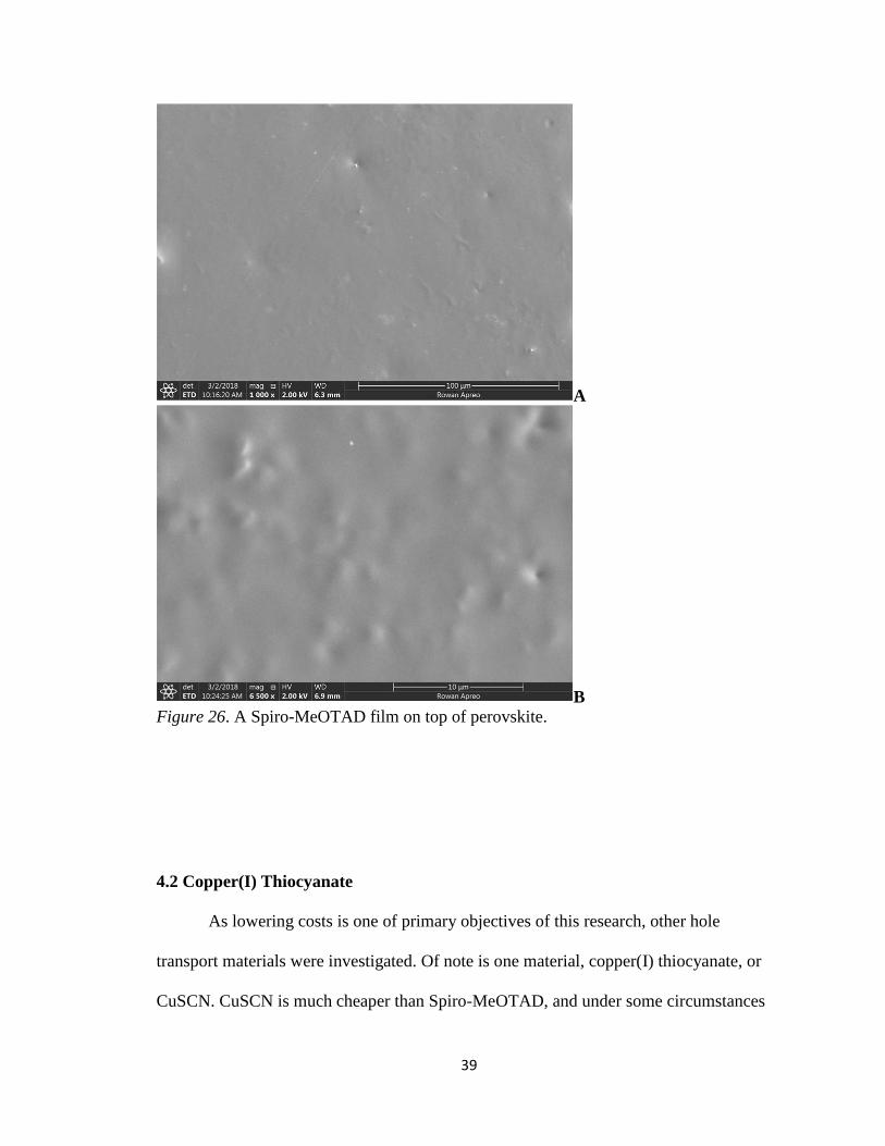
the film, and figure 26 shows SEM images of this film. Image (a) is an overall view while
image (b) is a higher magnification. There are no pinholes present, which shows good
uniformity, and recombination is not happening with the ETL through the perovskite.
39
A
B
Figure 26. A Spiro-MeOTAD film on top of perovskite.
4.2 Copper(I) Thiocyanate
As lowering costs is one of primary objectives of this research, other hole
transport materials were investigated. Of note is one material, copper(I) thiocyanate, or
CuSCN. CuSCN is much cheaper than Spiro-MeOTAD, and under some circumstances

40
may perform better [40]. CuSCN was prepared as in the literature, using ethyl sulfide as a
solvent. A reduced graphene oxide (rGO) spacer was also prepared as in the literature,
though it took far longer than stated, nearly four days to dissolve rGO in the desired
amount of chlorobenzene, instead of a half hour. A CuSCN hole transport layer was
deposited by dipping already fabricated perovskite films on substrates into the previously
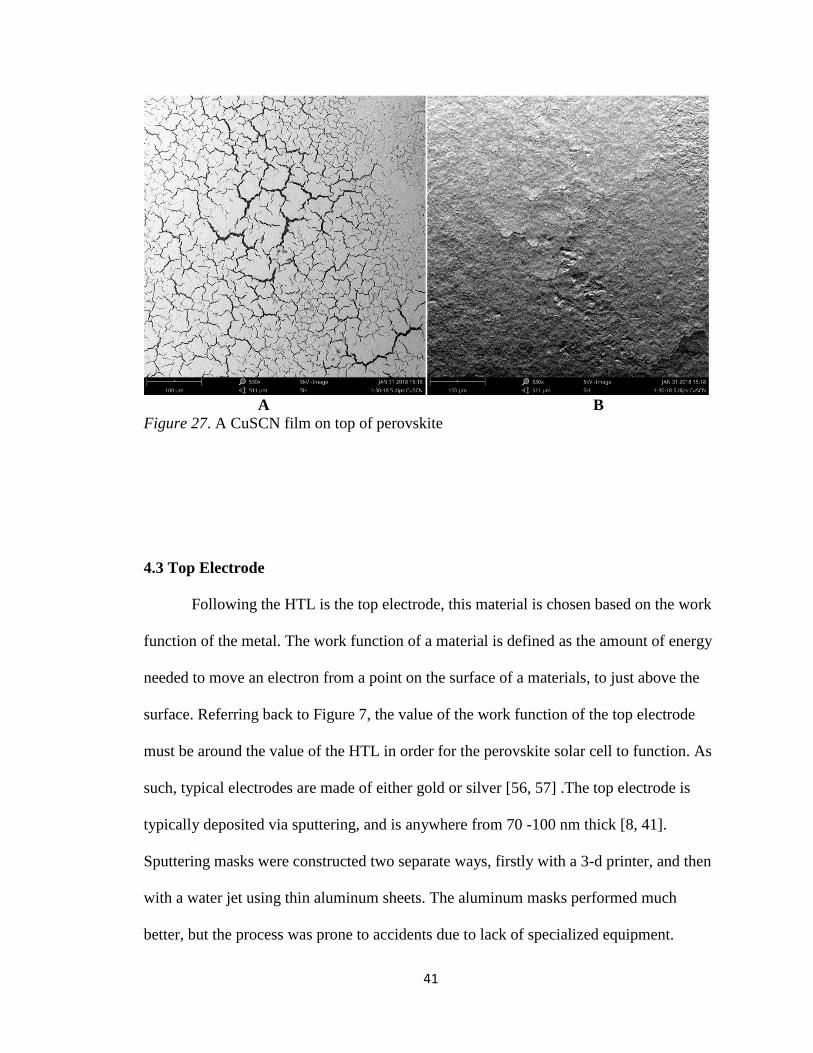
prepared CuSCN solution. The CuSCN did not want to stick to the perovskite after one
dip, but after two dips the film was much too thick. Changing the concentration made the
film quality worse, with large crystals of CuSCN forming, which degraded the
perovskite. Drip coating was also attempted, but the films were much too thick after
drying. Figure 27 shows two different types of SEM images of this film. Image (a) shows
the many cracks present, while image (b) shows that the cracks to not appear when only
looking at a topographical view. These multiple cracks which are present in the CuSCN
film could not be fixed with more dips. A decision was made to stick with Spiro-
MeOTAD, as this is the standard for hole-transport materials in this field.
41
A B
Figure 27. A CuSCN film on top of perovskite
4.3 Top Electrode
Following the HTL is the top electrode, this material is chosen based on the work
function of the metal. The work function of a material is defined as the amount of energy
needed to move an electron from a point on the surface of a materials, to just above the
surface. Referring back to Figure 7, the value of the work function of the top electrode
must be around the value of the HTL in order for the perovskite solar cell to function. As
such, typical electrodes are made of either gold or silver [56, 57] .The top electrode is
typically deposited via sputtering, and is anywhere from 70 -100 nm thick [8, 41].
Sputtering masks were constructed two separate ways, firstly with a 3-d printer, and then
with a water jet using thin aluminum sheets. The aluminum masks performed much
better, but the process was prone to accidents due to lack of specialized equipment.
42
First, silver was used as the top electrode, as it is much cheaper than gold. This
left the silver prone to oxidizing, which happened multiple times due to things like a
broken seal, or the inert argon gas running out. Also, the silver target used was burned
through, which showed the biggest flaws in the scalability of sputtering. Due to these
inherent problems, an alternative was investigated. Two-part silver epoxy was purchased
to connect the top electrode to a wire. The epoxy could not be directly placed onto the
cell and cured, as it cuts through the cell to the bottom electrode. A channel was created
on a glass slide using clear tape, and the silver epoxy was placed into this channel and
then smoothed over with a glass rod. After curing, this created a patch of silver on the
glass which was as thick as the channel it was placed in. This could then be placed faced
down on top of a fully constructed cell and clamped together. Though results using the
paste were not as consistent of efficient as those obtained using sputtering, it is worth
investigating in the future in order to lower production costs.
4.4 Testing
Completed cells were tested using a keithley 2450 sourcemeter, under a Newport
solar simulator. The solar simulator was 700watts per m2 on average, but due to
variations, the exact measurement was taken each time. As a control, multiple silicon
based cells were tested before each perovskite cell, and any offsets obtained were applied
to the perovskite. For example, a silicon cell which normally produces 2.5 V and 200 mA
under ambient sunlight would only produce 2.3 V and 30 mA under the simulator. The
application of this offset was a key component to obtaining accurate results. As of now,
only a slight photo response was seen, with a distinct voltage, but lacking current. Future
research will attempt to address this problem.

43
Chapter 5
Conclusions and Future Works
Perovskite solar cells represent a cheaper alternative to silicon based solar cells.
Though efficiencies are currently low, there are explainable reasons, which can be fixed.
Firstly, zinc oxide as an ETL may work, but it is far outperformed by mesoporous
titanium dioxide. Along with this, amorphous zinc oxide does not have a compact layer
followed by a mesoporous layer, which can lead to recombination effects. Of note is the
fact that zinc oxide has seen less use in the last year where perovskite solar cells are
concerned. Even though titanium dioxide requires a higher annealing temperature, and
therefore higher cost, it may still be worth it to use over zinc oxide, if the substrate can
withstand the high annealing temperatures. More investigations should be conducted on
the differences in performance between ZnO and TiO2, in order to decide which is best.
Perovskite solar cells fabricated via dip coated show promise for the future. Using
the methods described previously, a uniform layer of perovskite can be prepared quite
easily. Two step dip coating using a solvent is a quick process which is can be easily
scaled up to a much larger area. A short annealing step at 120°C allows for full formation
of the perovskite to complete, and results in a film which has no holes present. These
steps were also completed in ambient air, and cells were stable if sealed using silicone
sealant, or kept in a desiccator if unsealed. Thickness appears relatively constant
throughout the film, and is dependent on the number of dips, dipping angle, concentration
of the solution, and the length of time of each dip. By optimizing these parameters to
obtain the best thickness, this process can easily be automated, which can bring
production costs to a minimum. Lowering the annealing temperature to be compatible
with bendable substrates would also have a huge impact on the feasibility of perovskite

44
solar cells. This would allow cells to be placed on things such as automobiles and
airplanes, as well as uniquely designed buildings which are not compatible with the rigid
silicon cells that are currently available. Spray coating, while not viable using the
method described here, is another method in which costs may be lowered to a feasible
level. By using a finer mist, such as one provided by spray pyrolysis, a more uniform film
could be fabricated without micro rods present. It may also be worth it to investigate
electrostatic coating of lead iodide, as this is a very mature process already used to create
thin films on an industrial scale. Completed films of lead iodide can be bathed in MAI
and then allowed to anneal, which is a relatively simple process.
On terms of scalability, the currently used Spiro-MeOTAD as a material for the
HTL is the most expensive, and degrades the most rapidly. Methods of recovering unused
material should be investigated and optimized before proceeding to large scale
fabrication. DMSO and ethanol may provide possible paths to recrystallization and
purification of unused Spiro-MeOTAD, which can cut costs drastically. The dopants used
with the Spiro-MeOTAD are inexpensive comparatively, but recovery of these materials
should also be investigated. Dip coating must also be optimized with this layer, as the
methods discussed previously were drip coating based. The use of CuSCN as a material
for the HTL did not show promising results. A different solvent for the CuSN other than
ethyl sulfide should be investigated, as the CuSCN was prone to crystallization over a
large area when used with dip coating. It may be possible that a different method of
fabrication would solve this problem, so this should be investigated as well. CuSCN is
drastically cheaper than Spiro-MeOTAD, so investigating any possible alternatives are
worth it from a development standpoint. Research specific to the materials of the HTL

45
should be conducted, as this layer and its interactions with the perovskite layer are poorly
understood, and insight into the underlying physics of Spiro-MeOTAD would be
beneficial.
As currently produced perovskite cells rely on sputtering for the deposition of the
top electrode, this is an inherently flaw in their scalability. Regardless of the materials
used, sputtering is an expensive process requiring specialized equipment, and typically
used to cover relatively small areas. Sputtering over a large area is possible, but not
feasible to compete with current silicon solar cell technology. The results discussed here,
and in previous works, lend credibility to the use of a separate fabrication process for
larger sale. The use of a foil or paste as a top electrode produces comparable results to
those obtained from sputtering. Using gold, silver, or aluminum are all viable due to their
similar work functions, and creating a performance vs. cost analysis would be useful to
decide which material would be best to use. When looking at how perovskite solar cells
are tested, results can vary widely based on whether the test was forward or reverse bias,
as well as scan speed. Creating a standard way to test perovskite solar cells would be
extremely beneficial to the industry. Some cells perform much better if tested under dark
conditions first, and then light, or vice-versa. Light soaking and internal capacitance are
also factors which can cause measurements to be inaccurate. This has caused many
researches to pick and choose only their best results, and will be a compounding problem
if not quickly resolved. An underlying investigation should be conducted on the
hysteresis effects of perovskite solar cells, as understanding the mechanisms which cause
this could lead to higher efficiencies and more stable cells.

46
Recombination effects in perovskite solar cells is one of the biggest issues when
concerning efficiency. If holes and electrons are allowed to recombine inside the cell,
then a potential difference is not created and the cell ceases to function. It is now
understood that most recombination happens due to pinholes in the varying layers of the
solar cell. If there are pinholes present at any stage, then films may mesh with one
another at undesirable locations, which will lead to recombination. If the HTL and ETL
are allowed to touch, or somehow bypass one another to touch the opposite electrode,
then recombination happens at this junction. Annealing of each layer appears to be a key
aspect in preventing pinholes, which was seen most in the perovskite layer itself. An
optimization problem can be constructed which is dependent on the length of time and
temperature of the annealing step, to determine cost vs. efficiency for this process.
As most current perovskite solar cells are based on MAI and lead, other chemicals
should be investigated. This is due to the fact that MAI is synthesized using two
chemicals, hydroiodic acid, and methylamine which are on the United States Drug
Enforcement Administration list of schedule 1 controlled substances. Because of this, it
can be hard to obtain the required chemicals for large scale manufacturing as schedule 1
licenses must be obtained to do so. Along with this, many of the best performing
perovskite solar cells contain lead. As such, alternates for this should be investigated
using similar elements. By using the Goldschmidt tolerance factor as an initial guide, an
optimization problem can be formulated to find out possible combinations of elements
which constitute the general ABX3 form of a perovskite based on their ionic radii. Using
the tolerance factor as a guide, A-site modifications can be chosen from there based on
their similarity to methylamine. So far, tert-butylamine has been experimentally verified

47
in also producing a photo response, still using lead as the B site, and iodine as the X site.
Other elements similar to lead may be considered for B site modifications, such as tin or
bismuth. Along with these, X site modifications can be conducted using other halogens,
such as chlorine or bromine. Using these constraints, a list of possible cubic perovskite
can be defined, which can then be tests for photo responsiveness. From there, using
constraints such as cost and volatility, an optimal perovskite may be defined when
looking at cost of fabrication versus efficiency.
48
References
1. Petroleum, B., BP Statistical Review of World Energy June 2017. 2017(66).
2. Administration, E.I., eia Levelised Cost of Electricity. 2017.
3. Laboratory, N.R.E., Best Research-Cell Efficiencies. 2017.
4. Kojima, A., et al., <Organometal Halide Perovskites as Visible-Light Sensitizers
for Photovoltaic.pdf>. J Am Chem Soc, 2009(131): p. 6050-6051.
5. Johnsson, M. and P. Lemmens, Perovskites and thin films-crystallography and
chemistry. J Phys Condens Matter, 2008. 20(26): p. 264001.
6. Sato, T., et al., Extending the applicability of the Goldschmidt tolerance factor to
arbitrary ionic compounds. Sci Rep, 2016. 6: p. 23592.
7. Liu, X., R. Hong, and C. Tian, Tolerance factor and the stability discussion of
ABO3-type ilmenite. Journal of Materials Science: Materials in Electronics, 2008.
20(4): p. 323-327.
8. Liu, D. and T.L. Kelly, Perovskite solar cells with a planar heterojunction
structure prepared using room-temperature solution processing techniques.
Nature Photonics, 2013. 8: p. 133.
9. Ye, M., et al., Recent advances in interfacial engineering of perovskite solar cells.
Journal of Physics D: Applied Physics, 2017. 50(37).
10. Shockley, W. and H.J. Queisser, Detailed Balance Limit of Efficiency of p‐n
Junction Solar Cells. Journal of Applied Physics, 1961. 32(3): p. 510-519.
11. Fu, W., et al., Controlled crystallization of CH 3 NH 3 PbI 3 films for perovskite
solar cells by various PbI 2 (X) complexes. Solar Energy Materials and Solar
Cells, 2016. 155: p. 331-340.

49
12. Kulkarni, S.A., et al., Band-gap tuning of lead halide perovskites using a
sequential deposition process. J. Mater. Chem. A, 2014. 2(24): p. 9221-9225.
13. Hao, F., et al., Anomalous band gap behavior in mixed Sn and Pb perovskites
enables broadening of absorption spectrum in solar cells. J Am Chem Soc, 2014.
136(22): p. 8094-9.
14. Liu, J., et al., High-Quality Mixed-Organic-Cation Perovskites from a Phase-Pure
Non-stoichiometric Intermediate (FAI)1- x -PbI2 for Solar Cells. Adv Mater,
2015. 27(33): p. 4918-23.
15. Bishop, J.E., et al., Spray-cast multilayer perovskite solar cells with an active-
area of 1.5 cm2. Scientific Reports, 2017. 7(1): p. 7962.
16. Zheng, J., et al., Spin-coating free fabrication for highly efficient perovskite solar
cells. Solar Energy Materials and Solar Cells, 2017. 168: p. 165-171.
17. Sandstrom, A., et al., Spraying light: ambient-air fabrication of large-area
emissive devices on complex-shaped surfaces. Adv Mater, 2014. 26(29): p. 4975-
80.
18. Hwang, K., et al., Toward Large Scale Roll-to-Roll Production of Fully Printed
Perovskite Solar Cells. Advanced Materials, 2015. 27(7): p. 1241-1247.
19. Liu, G., et al., A red anatase TiO2 photocatalyst for solar energy conversion.
Energy & Environmental Science, 2012. 5(11): p. 9603.
20. Zhao, X., et al., Aluminum-Doped Zinc Oxide as Highly Stable Electron
Collection Layer for Perovskite Solar Cells. ACS Appl Mater Interfaces, 2016.
8(12): p. 7826-33.
21. Roiati, V., et al., Stark effect in perovskite/TiO2 solar cells: evidence of local
interfacial order. Nano Lett, 2014. 14(4): p. 2168-74.
50
22. Giordano, F., et al., Enhanced electronic properties in mesoporous TiO2 via
lithium doping for high-efficiency perovskite solar cells. Nature Communications,
2016. 7: p. 10379.
23. Park, H., et al., Surface modification of TiO2 photocatalyst for environmental
applications. Journal of Photochemistry and Photobiology C: Photochemistry
Reviews, 2013. 15: p. 1-20.
24. Yang, G., et al., Preparation of highly visible-light active N-doped TiO2
photocatalyst. Journal of Materials Chemistry, 2010. 20(25): p. 5301.
25. Etgar, L., et al., Mesoscopic CH3NH3PbI3/TiO2 heterojunction solar cells. J Am
Chem Soc, 2012. 134(42): p. 17396-9.
26. Kwon, Y.B., et al., Formation of ZnO thin films consisting of nano-prisms and
nano-rods with a high aspect ratio by a hydrothermal technique at 60 °C. Current
Applied Physics, 2011. 11(1): p. S197-S201.
27. Gu, Y., et al., Quantum confinement in ZnO nanorods. Applied Physics Letters,
2004. 85(17): p. 3833-3835.
28. Yamabi, S. and H. Imai, Growth conditions for wurtzite zinc oxide films in
aqueous solutions. Journal of Materials Chemistry, 2002. 12(12): p. 3773-3778.
29. Battisha, I.K., et al., Semiconductor ZnO Nano-Rods Thin Film Grown on Silver
Wire for Hemoglobin Biosensor Fabrication. New Journal of Glass and Ceramics,
2015. 05(02): p. 9-15.
30. Su, Y.K., et al., Ultraviolet ZnO nanorod photosensors. Langmuir, 2010. 26(1): p.
603-6.
31. Witkowski, B.S., et al., Ultra-fast growth of the monocrystalline zinc oxide
nanorods from the aqueous solution. International Journal of Nanotechnology,
2014. 11(9-1011): p. 758-772.

51
32. Das, R., et al., Controllable gold nanoparticle deposition on carbon nanotubes
and their application in immunosensing. RSC Advances, 2015. 5(60): p. 48147-
48153.
33. Farley, N.R.S., et al., Sol-gel formation of ordered nanostructured doped ZnO
films. Journal of Materials Chemistry, 2004. 14(7): p. 1087.
34. Ong, B.S., et al., Stable, Solution-Processed, High-Mobility ZnO Thin-Film
Transistors. Journal of the American Chemical Society, 2007. 129(10): p. 2750-
2751.
35. Kar, S. and S. Kundoo, Synthesis and Characterization of Zinc Oxide Thin Films
by Sol-Gel Dip Coating Technique. 2014.
36. Paul, G.K., et al., Structural, optical and electrical studies on sol–gel deposited Zr
doped ZnO films. Materials Chemistry and Physics, 2003. 79(1): p. 71-75.
37. Ivanova, T., et al., Study of ZnO sol–gel films: Effect of annealing. Materials
Letters, 2010. 64(10): p. 1147-1149.
38. Hafdallah, A., et al., In doped ZnO thin films. Journal of Alloys and Compounds,
2011. 509(26): p. 7267-7270.
39. O'Brien, P., T. Saeed, and J. Knowles, Speciation and the nature of ZnO thin films
from chemical bath deposition. Journal of Materials Chemistry, 1996. 6(7): p.
1135-1139.
40. Arora, N., et al., Perovskite solar cells with CuSCN hole extraction layers yield
stabilized efficiencies greater than 20%. Science, 2017. 358(6364): p. 768-771.
41. Chen, H., et al., Enhanced Performance of Planar Perovskite Solar Cells Using
Low-Temperature Solution-Processed Al-Doped SnO2 as Electron Transport
Layers. Nanoscale Research Letters, 2017. 12(1): p. 238.

52
42. Dobrozhan, O., et al., Substructural investigations, Raman, and FTIR
spectroscopies of nanocrystalline ZnO films deposited by pulsed spray pyrolysis.
physica status solidi (a), 2015. 212(12): p. 2915-2921.
43. Yang, M., et al., Square-Centimeter Solution-Processed Planar CH3NH3PbI3
Perovskite Solar Cells with Efficiency Exceeding 15%. Advanced Materials, 2015.
27(41): p. 6363-6370.
44. Fang, R., et al., The rising star in photovoltaics-perovskite solar cells: The past,
present and future. Science China Technological Sciences, 2016. 59(7): p. 989-
1006.
45. Kramer, I.J., et al., Efficient Spray-Coated Colloidal Quantum Dot Solar Cells.
Advanced Materials, 2015. 27(1): p. 116-121.
46. Wu, Y., et al., Retarding the crystallization of PbI2 for highly reproducible
planar-structured perovskite solar cells via sequential deposition. Energy
Environ. Sci., 2014. 7(9): p. 2934-2938.
47. Ying, C., et al., A two-layer structured PbI2 thin film for efficient planar
perovskite solar cells. Nanoscale, 2015. 7(28): p. 12092-5.
48. Burschka, J., et al., Sequential deposition as a route to high-performance
perovskite-sensitized solar cells. Nature, 2013. 499: p. 316.
49. Bi, D., et al., Efficient luminescent solar cells based on tailored mixed-cation
perovskites. Science Advances, 2016. 2(1).
50. Nenon, D.P., et al., Structural and chemical evolution of methylammonium lead
halide perovskites during thermal processing from solution. Energy &
Environmental Science, 2016. 9(6): p. 2072-2082.
51. Zhang, X., et al., High-efficiency perovskite solar cells prepared by using a
sandwich structure MAI-PbI2-MAI precursor film. Nanoscale, 2017. 9(14): p.
4691-4699.
53
52. Ding, I.K., et al., Pore-Filling of Spiro-OMeTAD in Solid-State Dye Sensitized
Solar Cells: Quantification, Mechanism, and Consequences for Device
Performance. Advanced Functional Materials, 2009. 19(15): p. 2431-2436.
53. Fabregat-Santiago, F., et al., Electron Transport and Recombination in Solid-State
Dye Solar Cell with Spiro-OMeTAD as Hole Conductor. Journal of the American
Chemical Society, 2009. 131(2): p. 558-562.
54. Jeon, N.J., et al., o-Methoxy substituents in spiro-OMeTAD for efficient
inorganic-organic hybrid perovskite solar cells. J Am Chem Soc, 2014. 136(22):
p. 7837-40.
55. Shi, D., et al., Spiro-OMeTAD single crystals: Remarkably enhanced charge-
carrier transport via mesoscale ordering. Science Advances, 2016. 2(4).
56. Zhang, B., W. Xie, and Y. Xiang, Development and Prospect of
Nanoarchitectured Solar Cells. International Journal of Photoenergy, 2015. 2015:
p. 1-11.
57. Noh, J.H., et al., Nanostructured TiO2/CH3NH3PbI3 heterojunction solar cells
employing spiro-OMeTAD/Co-complex as hole-transporting material. Journal of
Materials Chemistry A, 2013. 1(38): p. 11842.