pericom product datasheet - pll clock driver for …a6 a5 a4 a3 a2 a1 a0 w/r 1 1 0 1 1 1 0 0/1 data...
TRANSCRIPT

1All trademarks are property of their respective owners. www.diodes.com 01/06/17
Block Diagram Pin Configuration
DescriptionThe PI6C20400B is a PCIe 3.0 compliant high-speed, low-noise differential clock buffer designed to be companion to PCIe 3.0 clock generator. It is backward compatible with PCIe 1.0 and 2.0 specification. The device distributes the differential SRC clock from PCIe 3.0 clock generator to four differential pairs of clock outputs either with or without PLL. The clock outputs are controlled by input selection of SRC_STOP#, PWRDWN# and SMBus, SCLK and SDA. When input of either SRC_STOP# or PWRDWN# is low, the output clocks are Tristated. When PWRDWN# is low, the SDA and SCLK inputs must be Tri-stated.
Features ÎÎ Phase jitter filter for PCIe 3.0 applicationÎÎ Four Pairs of Differential ClocksÎÎ Low skew < 50psÎÎ Low jitter < 50ps cycle-to-cycleÎÎ < 1 ps additive RMS phase jitterÎÎ Output Enable for all outputsÎÎ Outputs tristate control via SMBusÎÎ Programmable PLL BandwidthÎÎ 100 MHz PLL Mode operationÎÎ 100 - 400 MHz Bypass Mode operationÎÎ 3.3V OperationÎÎ Packaging (Pb-free and Green):
-28-Pin SSOP (H28) -28-Pin TSSOP (L28)
OUT0OUT0#
OUT1OUT1#
OUT2OUT2#
OUT3OUT3#
DIV
OutputControl
SMBusController
PLLPLL_BW#
SRCSRC#
PLL/BYPASS#
SCLKSDA
OE_INVOE_0 & OE_3SRC_STOP#
PWRDWN#
VDD_AVSS_AIREFOE_INVVDDOUT3OUT3#OE_3OUT2OUT2#VDDPLL_BW#SRC_STOP#PWRDWN#
2827262524232221201918171615
1234567891011121314
VDDSRC
SRC#VSSVDD
OUT0OUT0#
OE_0OUT1
OUT1#VDD
PLL/BYPASS#SCLK
SDA
A product Line ofDiodes Incorporated
PI6C20400B
1:4 Clock Driver for Intel PCIe® 3.0 Chipsets
17-0006

2All trademarks are property of their respective owners. www.diodes.com 01/06/17
A product Line ofDiodes Incorporated
PI6C20400B
Serial Data Interface (SMBus) This part is a slave only SMBus device that supports indexed block read and indexed block write protocol using a single 7-bit address and read/write bit as shown below.
Pinout Table
Pin# Pin Name Type Description
2, 3 SRC & SRC# Input 0.7V Differential SRC input from PI6C410 clock synthesizer
8, 21 OE_0 & OE_3 Input3.3V LVTTL input for enabling outputs, active high. OE_0 for OUT0 / OUT0#OE_3 for OUT3 / OUT3#
25 OE_INV Input
3.3V LVTTL input for inverting the OE, SRC_STOP# and PWRDWN# pins. When 0 = same stageWhen 1 = OE_0, OE_3, SRC_STOP#, PWRDWN# inverted.
6, 7, 9, 10, 19, 20, 22, 23 OUT[0:3] & OUT[0:3]# Output 0.7V Differential outputs
12 PLL/BYPASS# Input 3.3V LVTTL input for selecting fan-out of PLL operation.13 SCLK Input SMBus compatible SCLOCK input14 SDA I/O SMBus compatible SDATA26 IREF Input External resistor connection to set the differential output current16 SRC_STOP# Input 3.3V LVTTL input for SRC stop, active low17 PLL_BW# Input 3.3V LVTTL input for selecting the PLL bandwidth15 PWRDWN# Input 3.3V LVTTL input for Power Down operation, active low1, 5, 11, 18, 24 VDD Power 3.3V Power Supply for Outputs4 VSS Ground Ground for Outputs27 VSS_A Ground Ground for PLL28 VDD_A Power 3.3V Power Supply for PLL
Address AssignmentA6 A5 A4 A3 A2 A1 A0 W/R1 1 0 1 1 1 0 0/1
Data Protocol1 bit 7 bits 1 1 8 bits 1 8 bits 1 8 bits 1 8 bits 1 1 bit
Start bit
Slave Addr R/W Ack Register
offset AckByte Count = N
Ack Data Byte 0 Ack …
Data Byte N - 1
Ack Stop bit
Notes:
1. Register offset for indicating the starting register for indexed block write and indexed block read. Byte Count in write mode cannot be 0.
17-0006

3All trademarks are property of their respective owners. www.diodes.com 01/06/17
A product Line ofDiodes Incorporated
PI6C20400B
Data Byte 0: Control Register
Bit Descriptions Type Power Up Condition Output(s) Affected Source Pin
0Outputs Mode0 = Divide by 21 = Normal
RW 1 = Normal OUT[0:3], OUT[0:3]# NA
1PLL/BYPASS#0 = Fanout1 = PLL
RW 1 = PLL OUT[0:3], OUT[0:3]# NA
2PLL Bandwidth0 = High Bandwidth,1 = Low Bandwidth
RW 1 = Low OUT[0:3], OUT[0:3]# NA
3 Reserved NA4 Reserved NA5 Reserved NA
6SRC_STOP#0 = Driven when stopped1 = Tristate
RW 0 = Driven when stopped OUT[0:3], OUT[0:3]# NA
7PWRDWN#0 = Driven when stopped1 = Tristate
RW 0 = Driven when stopped OUT[0:3], OUT[0:3]# NA
Data Byte 1: Control Register
Bit Descriptions Type Power Up Condition Output(s) Affected Source Pin
0 Reserved NA
1 OUTPUTS enable1 = Enabled 0 = Disabled
RW 1 = Enabled OUT0, OUT0# NA
2 RW 1 = Enabled OUT1, OUT1# NA
3 Reserved NA4 Reserved NA5 OUTPUTS enable
1 = Enabled 0 = Disabled
RW 1 = Enabled OUT2, OUT2# NA
6 RW 1 = Enabled OUT3, OUT3# NA
7 Reserved NA
17-0006

4All trademarks are property of their respective owners. www.diodes.com 01/06/17
A product Line ofDiodes Incorporated
PI6C20400B
Data Byte 2: Control Register
Bit Descriptions Type Power Up Condition Output(s) Affected Source Pin
0 Reserved NA
1 Allow control of OUTPUTS with assertion of SRC_STOP#0 = Free running1 = Stopped with SRC_Stop#
RW 0 = Free running OUT0, OUT0# NA
2 RW 0 = Free running OUT1, OUT1# NA
3 Reserved NA4 Reserved NA5 Allow control of OUTPUTS with
assertion of SRC_STOP#0 = Free running1 = Stopped with SRC_Stop#
RW 0 = Free running OUT2, OUT2# NA
6 RW 0 = Free running OUT3, OUT3# NA
7 Reserved NA
Data Byte 3: Control Register
Bit Descriptions Type Power Up Condition Output(s) Affected Source Pin
0
Reserved
RW1 RW
2 RW
3 RW4 RW5 RW6 RW7 RW
Data Byte 3: Control Register
Bit Descriptions Type Power Up Condition Output(s) Affected Pin
0
Pericom ID
R 0 NA NA1 R 0 NA NA2 R 0 NA NA3 R 0 NA NA4 R 0 NA NA5 R 1 NA NA6 R 0 NA NA7 R 0 NA NA
17-0006

5All trademarks are property of their respective owners. www.diodes.com 01/06/17
A product Line ofDiodes Incorporated
PI6C20400B
Functionality
PWRDWN# OUT OUT# SRC_Stop# OUT OUT#
1 Normal Normal 1 Normal Normal0 IREF × 2 or Float Low 0 IREF × 6 or Float Low
Power Down (PWRDWN# assertion)
Power Down (PWRDWN# De-assertion)
PWRDWN#
OUT#OUT
PWRDWN#OUT
OUT#
Tdrive_PwrDwn#<300us, >200mV
Tstable<1ms
Figure 1. Power down sequence
Figure 2. Power down de-assert sequence
17-0006
6All trademarks are property of their respective owners. www.diodes.com 01/06/17
A product Line ofDiodes Incorporated
PI6C20400B
Differential Clock Output Current
Board Target Trace/Term Z Reference R, Iref = VDD/(3xRr) Output Current VOH @ Z
100Ω (100Ω differential ≈ 15% coupling ratio)
RREF = 475Ω 1%, IREF = 2.32mA
IOH = 6 x IREF 0.7V @ 50
0V
IOUT
0.85V
Slope ~ 1/Rs
RO
ROS
VOUT = 0.85V max
Iout
VDD(3.3V ± 5%)
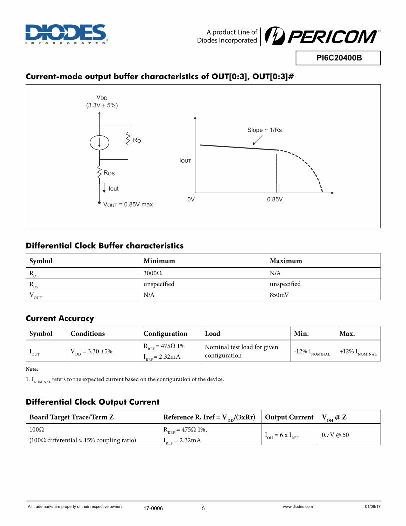
Current-mode output buffer characteristics of OUT[0:3], OUT[0:3]#
Differential Clock Buffer characteristics
Symbol Minimum Maximum
RO 3000Ω N/AROS unspecified unspecifiedVOUT N/A 850mV
Current Accuracy
Symbol Conditions Configuration Load Min. Max.
IOUT VDD = 3.30 ±5%RREF = 475Ω 1%IREF = 2.32mA
Nominal test load for given configuration -12% INOMINAL +12% INOMINAL
Note:
1. INOMINAL refers to the expected current based on the configuration of the device.
17-0006

7All trademarks are property of their respective owners. www.diodes.com 01/06/17
A product Line ofDiodes Incorporated
PI6C20400B
Absolute Maximum Ratings (Over operating free-air temperature range)
Symbol Parameters Min. Max. Units
VDD_A 3.3V Core Supply Voltage -0.5 4.6
VVDD 3.3V I/O Supply Voltage -0.5 4.6VIH Input High Voltage 4.6VIL Input Low Voltage -0.5 Ts Storage Temperature -65 150 °C
VESD ESD Protection 2000 V
Note:
1. Stress beyond those listed under “Absolute Maximum Ratings” may cause permanent damage to the device.
DC Electrical Characteristics (VDD = 3.3±5%, VDD_A = 3.3±5%)
Symbol Parameters Condition Min. Max. Units
VDD_A 3.3V Core Supply Voltage 3.135 3.465
VVDD 3.3V I/O Supply Voltage 3.135 3.465VIH 3.3V Input High Voltage VDD 2.0 VDD + 0.3VIL 3.3V Input Low Voltage VSS – 0.3 0.8IIL Input Leakage Current 0 < VIN < VDD -5 +5 µAVOH 3.3V Output High Voltage IOH = -1mA 2.4
VVOL 3.3V Output Low Voltage IOL = 1mA 0.4
IOH Output High CurrentIOH = 6 x IREF, IREF = 2.32mA
12.2mA
15.6CIN Input Pin Capacitance 3 5
pFCOUT Output Pin Capacitance 6LPIN Pin Inductance 7 nH
IDD(BYPASS)
Power Supply Current (PLL Bypass) VDD = 3.465V, FCPU = 100MHz 90
mAIDD Power Supply CurrentVDD = 3.465V Bypass mode 100FCPU = 100MHz PLL mode 130
ISS Power Down Current Driven outputs 40ISS Power Down Current Tristate outputs 12TA Ambient Temperature -40 85 °C
17-0006

8All trademarks are property of their respective owners. www.diodes.com 01/06/17
A product Line ofDiodes Incorporated
PI6C20400B
AC Switching Characteristics (VDD = 3.3±5%, VDD_A = 3.3±5%)
Symbol Parameters Condition Min. Typ. Max. Units
FIN
PLL Mode 95 105 MHzBypass Mode 100 400 MHz
Trise / Tfall2 Rise and Fall Time (measured be-
tween 0.175V to 0.525V) 175 700 ps
DTrise / DTfall2 Rise and Fall Time Variation 125 ps
Tpd
PLL Mode ±250 psNon-PLL Mode 2.5 6.5 ns
Tjitter3, 4 Cycle – Cycle Jitter 50 ps
VHIGH2 Voltage High including overshoot 660 1150 mV
VLOW2 Voltage Low including undershoot -300 mV
Vcross2 Absolute crossing point voltages 250 550 mV
DVcross2 Total Variation of Vcross over all edges 140 mV
TDC3 Duty Cycle 45 55 %
tjphPCIeG1
Phase Jitter, PLL Mode
PCIe Gen1 30 86 ps (p-p)
tjphPCIeG2
PCIE_2_0_8MHz_1_5M_H3_STEP, Low Freq. 0.7 3
ps (rms)
PCIE_2_0_8MHz_1_5M_H3_STEP, High Freq. 2 3.1
tjphPCIeG3
PCIE_3_0_2MHz_5M_H3_FIRST, Low Freq. 2 3
PCIE_3_0_2MHz_5M_H3_FIRST, High Freq. 0.47 1
tjphPCIeG1
Additive Phase Jitter, Bypass Mode
PCIe Gen1 0 0.001 ps (p-p)
tjphPCIeG2
PCIE_2_0_8MHz_1_5M_H3_FIRST, Low Freq. 0 0.001
ps (rms)
PCIE_2_0_8MHz_1_5M_H3_FIRST, High Freq. 0 0.001
tjphPCIeG3
PCIE_3_0_2MHz_5M_H3_FIRST, Low Freq. 0 0.001
PCIE_3_0_2MHz_5M_H3_FIRST, High Freq. 0 0.001
Notes:
1. Test configuration is Rs = 33.2Ω, Rp = 49.9Ω, and 2pF.
2. Measurement taken from Single Ended waveform.
3. Measurement taken from Differential waveform.
4. Measurement taken using M1 data capture analysis tool.
5. Additive jitter is calculated from input and output RMS phase jitter by using PCIe 2.0 filter. (Tjadd = √(output jitter)2 – (input jitter)2
17-0006

9All trademarks are property of their respective owners. www.diodes.com 01/06/17
A product Line ofDiodes Incorporated
PI6C20400B
Configuration Test Load Board Termination
475Ω1%
49.9Ω1%
Rp49.9Ω
1%
Rp
33Ω5%
Rs
33Ω5%
Rs
PI6C20400B
TLA
TLB
OUT
OUT#
2pF5%
2pF5%
17-0006

10All trademarks are property of their respective owners. www.diodes.com 01/06/17
A product Line ofDiodes Incorporated
PI6C20400B
Packaging Mechanical: 28-Pin SSOP (H)
1
: 28-Pin, 209-Mil Wide, SSOPNOITPIRCSED :EDOC EGAKCAP
1250-DP :# LORTNOC TNEMUCOD F:NOISIVER
80/01/40 :ETAD
H28
08-0143
17-0006

11All trademarks are property of their respective owners. www.diodes.com 01/06/17
A product Line ofDiodes Incorporated
PI6C20400B
Packaging Mechanical: 28-Pin TSSOP (L)
16-0076
Ordering Information(1-3)
Ordering Code Package Code Package Description
PI6C20400BHE H 28-pin, 209-mil wide (SSOP)PI6C20400BHEX H 28-pin, 209-mil wide (SSOP), Tape & ReelPI6C20400BLE L 28-pin, 173-mil wide (TSSOP)PI6C20400BLEX L 28-pin, 173-mil wide (TSSOP), Tape & Reel
Notes:
1. 1Thermal characteristics can be found on the company web site at www.pericom.com/packaging/
2. E = Pb-free and Green
3. Adding an X suffix = Tape/Reel
Note: For latest package info, please check: http://www.pericom.com/support/packaging/packaging-mechanicals-and-thermal-characteristics/
17-0006

12All trademarks are property of their respective owners. www.diodes.com 01/06/17
A product Line ofDiodes Incorporated
PI6C20400B
IMPORTANT NOTICE
DIODES INCORPORATED MAKES NO WARRANTY OF ANY KIND, EXPRESS OR IMPLIED, WITH REGARDS TO THIS DOCUMENT, INCLUDING, BUT NOT LIMITED TO, THE IMPLIED WARRANTIES OF MERCHANTABILITY AND FITNESS FOR A PARTICULAR PURPOSE (AND THEIR EQUIVALENTS UNDER THE LAWS OF ANY JURISDICTION).
Diodes Incorporated and its subsidiaries reserve the right to make modifications, enhancements, improvements, corrections or other changes without further no-tice to this document and any product described herein. Diodes Incorporated does not assume any liability arising out of the application or use of this document or any product described herein; neither does Diodes Incorporated convey any license under its patent or trademark rights, nor the rights of others. Any Customer or user of this document or products described herein in such applications shall assume all risks of such use and will agree to hold Diodes Incorporated and all the companies whose products are represented on Diodes Incorporated website, harmless against all damages.
Diodes Incorporated does not warrant or accept any liability whatsoever in respect of any products purchased through unauthorized sales channel.
Should Customers purchase or use Diodes Incorporated products for any unintended or unauthorized application, Customers shall indemnify and hold Diodes Incorporated and its representatives harmless against all claims, damages, expenses, and attorney fees arising out of, directly or indirectly, any claim of personal injury or death associated with such unintended or unauthorized application.
Products described herein may be covered by one or more United States, international or foreign patents pending. Product names and markings noted herein may also be covered by one or more United States, international or foreign trademarks.
This document is written in English but may be translated into multiple languages for reference. Only the English version of this document is the final and determi-native format released by Diodes Incorporated.
LIFE SUPPORT
Diodes Incorporated products are specifically not authorized for use as critical components in life support devices or systems without the express written approval of the Chief Executive Officer of Diodes Incorporated. As used herein:
A. Life support devices or systems are devices or systems which:
1. are intended to implant into the body, or
2. support or sustain life and whose failure to perform when properly used in accordance with instructions for use provided in the labeling can be reasonably expected to result in significant injury to the user.
B. A critical component is any component in a life support device or system whose failure to perform can be reasonably expected to cause the
failure of the life support device or to affect its safety or effectiveness.
Customers represent that they have all necessary expertise in the safety and regulatory ramifications of their life support devices or systems, and acknowledge and agree that they are solely responsible for all legal, regulatory and safety-related requirements concerning their products and any use of Diodes Incorporated products in such safety-critical, life support devices or systems, notwithstanding any devices- or systems-related information or support that may be provided by Diodes Incorporated. Further, Customers must fully indemnify Diodes Incorporated and its representatives against any damages arising out of the use of Diodes Incorporated products in such safety-critical, life support devices or systems.
Copyright © 2016, Diodes Incorporated
www.diodes.com
17-0006